Embed Size (px)
Citation preview

Minimum Supply Voltage of 2.45 GHz LCOscillator in 28 nm FD-SOI Process
Mariana Siniscalchi†, Nicolas Gammarano?, Carlos Galup-Montoro‡, Sylvain Bourdel§ and Fernando Silveira¶†?¶Instituto de Ingenierıa Electrica, Universidad de la Republica, Montevideo, Uruguay
‡UFSC, Electrical and Electronics Engineering Department, Florianopolis, Brazil§RFIC-Lab, Grenoble INP, Universite Grenoble Alpes, Grenoble, France
†[email protected], [email protected], ‡[email protected], §[email protected], ¶[email protected]
Abstract—The minimum supply voltage limit is studied in thecase of a 2.45 GHz LC cross-coupled oscillator, in a 28 nm FD-SOI technology. An approach with simple equations aided withlook up tables is used to obtain a theoretical prediction of theminimum voltage and current required for operation. The lookup tables are loaded with all the transistor parameters of interest,which are extracted by means of DC simulations. The predictionis in good agreement with the simulation results, as long as thetransition frequency of the transistors is at least 10 times theoscillation frequency. A feasible supply voltage for this circuittopology, oscillation frequency and technology is shown to be 37mV. Depending on the back-plane voltage value and the inductorselected, the supply voltage reduction is limited by either theparasitic capacitances or the intrinsic gain of the transistors.Equations are provided to aid the designer in the selection of allof the design parameters to achieve the lowest possible supplyvoltage and lowest possible current.
Index Terms—Ultra-Low Voltage, Low-Power Electronics, RF,FD-SOI
I. INTRODUCTION
Supplying energy to a device may entail very restrictivevoltage and power constraints. Thermal or electrochemicalharvesting devices provide very low voltages of the order of100 mV or even lower [1]–[3]. Furthermore, if the operationof circuits at those supply voltage levels is feasible this makespossible important reductions in consumed power and energy.
Here we target a cross-coupled LC oscillator that operatesat 2.45 GHz, the center frequency of the 2.4 GHz Industrial,Scientific and Medical (ISM) radio band. This radio bandis one of the most used RF frequency bands worldwide, asprotocols like Wi-Fi, Bluetooth and IEEE 802.15.4 work inthat band.
The oscillator is simulated in a 28 nm FD-SOI process.As the nanometer processes are complex to model, we usean approach based on analytic calculations and lookup tables(LUTs) [4], [5]. Thus, the complexity, in particular the shortchannel effects, are dealt with by using different LUTs de-pending on the target transistor size.
The oscillators in the range of GHz with lowest supplyvoltage operate from supplies as low as 0.35 to 0.41 V [6]–[8].Here, the minimum supply voltage limit is studied, showingthat it can be much further reduced and explaining what arethe constraints to do so. As a result, guidelines are providedto achieve the lowest supply voltage possible, as well asan accurate estimation of the minimum current consumptionrequired.
C1
L1
MN1
VDD
VX VY
MN0
Fig. 1. Circuit schematic of an LC cross-coupled oscillator.
II. STUDY OF THE MINIMUM OPERATING VOLTAGE LIMIT
The minimum supply voltage to enable oscillation is studiedherein in the case of an LC cross-coupled oscillator. Figure 1shows the circuit schematic of such oscillator. Each transistorintroduces 180° shift, so two transistors suffice for oscilla-tion [9].
This voltage biased topology is more suitable for ultra lowvoltage operation than a current biased topology, since thetransistors in the tail current source would not saturate. Inaddition, the voltage biased topology is useful in the ultralow voltage context, since the circuit is only connected tothe supply voltage, VDD, through the inductor. Therefore, fulladvantage is taken from the DC voltage by supplying it directlyto the transistors and having an output that may swing wellabove VDD [10].
The inductor L1 and the capacitor C1 can be considered astwo separate inductors L1/2 and two separate capacitors 2C1
in series respectively. In both cases, the middle node is con-nected to virtual signal ground due to the circuit’s symmetry.The oscillation angular frequency is ωosc = 1/
√L1C1. At the
oscillation frequency, the open-loop gain is
Aol (jωosc) =
(gm
2RP
+ go
)2
, (1)
where RP is the inductor L1 parallel resistance at the oscilla-tion frequency and gm and go are the transconductance and theoutput conductance of either transistor, respectively. Both arecalculated around the DC operating point VX = VY = VDD.The Barkhausen oscillation condition reduces to
gm ≥2
RP+ go. (2)
978-1-6654-2429-5/21/$31.00 ©2021 IEEE
2021
19t
h IE
EE In
tern
atio
nal N
ew C
ircui
ts a
nd S
yste
ms C
onfe
renc
e (N
EWC
AS)
| 97
8-1-
6654
-242
9-5/
20/$
31.0
0 ©
2021
IEEE
| D
OI:
10.1
109/
NEW
CA
S506
81.2
021.
9462
789

The oscillation condition does not depend explicitly on thesupply voltage, but through the parameters gm and go whichdepend on the bias voltage.
(2) simplifies to a condition on the drain current
ID ≥2
RP
gmID− go
ID
, (3)
where gm/ID and go/ID are looked up in a table. Thislookup table (LUT) must be filled in advance by means ofDC simulations of a unitary transistor.
A. Design of the transistors
The lvtnfet rf devices are the nMOS transistors of choice,since these have a lower threshold voltage than the standardnfet and are characterized for RF operation.
To minimize the capacitance contribution, the minimumchannel length L = 30 nm is used (following some of thesuggestions in Section 8.8 of [9]).
Both transistors are implemented with N fingers of widthWu = 206 nm. Thus, the total width is W = N ×Wu. Thisallows the designer to extract the LUT only in the case of atransistor of L = 30 nm and Wu = 206 nm. Then the designercan obtain in a simple way the parameters of a transistor withN fingers, by means of multiplying by N .
Thus, the values in the LUT are loaded for L = 30 nm,Wu = 206 nm and the values of VDD and back plane voltageVBP of interest, provided that in DC VGS = VDS = VDD.
As a consequence,
ID = N × IDu, (4)
where IDu is the drain current through a single finger. From(3) and (4), it follows that there is a minimum number offingers N required for oscillation at 2.45 GHz, given by
Nmin =
(1
IDu
)( 2RP
gmID− go
ID
). (5)
Note that N ≥ 0 if gm/ID > go/ID. Then, gm/go >1, which sets a lower boundary for the intrinsic gain of thetransistor.
B. Inductor choice
The inductor that achieves the lowest losses at the operatingfrequency must be used to reduce the power consumptionof the oscillator. This is because the active devices of theoscillator must compensate for the losses of the LC tank andbecause the inductor is the most lossy part of the tank inintegrated technologies.
There are four kinds of inductors available in the library.The achievable inductance values using the single turn coilsare in the range from 0.091 nH to 1.2 nH, while using the multiturn coils the achievable values are in the range from 0.61 nHto 7.76 nH. These two kinds (single and multi turn coils) havetheir differential and non-differential version. Here the multiturn coils are chosen, to use higher values of inductors thatachieve a higher quality factor Q. The differential coils arechosen to keep the circuit symmetric.
Fig. 2. Inductance value L1 as a function of frequency of a given inductorin the library with 11 µm coil width.
Fig. 3. Parasitic parallel resistor RP as a function of frequency of a giveninductor of the library with 11 µm coil width.
The parameters of the inductors in the library were ex-tracted for several values of the intended nominal inductance.The equivalent parallel resistance is extracted as RP =1/Re (YL1
), the inductance value is extracted as L1 =−1/ (2πf Im (YL1)) and Q = RP / (2πfL1). The results areplotted in Figs. 2 to 4, as a function of frequency.
The coil width used in these simulations is 11 µm. More-over, the dependence of the coil parameters on its width isnegligible, according to simulations (omitted here).
According to (3), the highest RP the lowest the minimumID. The maximum value of RP diminishes with frequency,as seen in Fig. 3. Therefore, the Lnom = 7.76 nH nomi-nal inductor is selected because it has the lowest losses at2.45 GHz, which correspond to the highest RP = 1.6 kΩ and
Fig. 4. Quality factor Q as a function of frequency of a given inductor ofthe library with 11 µm coil width.

100 200 300 400 500VDD (mV)
20
40
60
80
100
120
140
160
180ID
Qm
in (
A)IDQmin predicted (LUT)IDQmin simulated
101
102
103
104
Nm
in (t
rans
istor
s in
para
llel)
Nmin predicted (LUT)Nmin simulated
Fig. 5. The minimum current and number of transistors in parallel foroscillation at 2.45GHz as a function of VDD for VBP = 0V. Simulationresults and results predicted by (3) and (5) and the LUT.
L1 = 9.63 nH. Note that the 7.76 nH nominal inductor is notthe highest Q inductor, according to Fig. 4.
III. METHODOLOGY
Given VDD and VBP , the minimum current to enableoscillation can be obtained by means of following (3) togetherwith the LUT (gm/ID and go/ID).
The oscillator simulated includes the 7.76 nH nominal in-ductor selected in Section II-B, an ideal capacitor C1 tomatch the oscillation frequency to 2.45 GHz and two identicalparallel arrangements of N transistors of L = 30 nm andWu = 206 nm.
For each value of VDD and VBP of interest, N and C1
are modified to obtain, through periodic steady-state (PSS)simulations, the minimum N for oscillation at 2.45 GHz.Thus, obtaining the minimum ID.
Finally, the simulation results of ID are compared to theboundary predicted by (3) together with the LUT.
IV. RESULTS
The current through the transistors ID and the number offingers N , are compared to those predicted by (3) and (5),respectively, and the LUT. The results are shown in Fig. 5 forVBP = 0 V and in Fig. 6 for VBP = 3 V.
On the one hand, the simulation results for VBP = 3 V arewell predicted for all the values of VDD.
On the other hand, the results for VBP = 0 V show thatthe prediction is good for VDD ≥ 275 mV and it worsens asVDD decreases. In order to understand up to what extent isit possible to make these predictions, the transition frequencyfT of the transistors is included in the LUT. Figure 7 showshow fT depends on VBP and VDD.
If fT is too small, the simple small signal model used tomake the predictions would not be accurate at the 2.45 GHzoperating frequency. As a rule of thumb, fT should be atleast one decade above the operating frequency, thus fT >24.5 GHz [11]. This means that, the results are likely tobe accurate for VDD ≥ 275 mV if VBP = 0 V and for
100 200 300 400 500VDD (mV)
100
200
300
400
500
IDQ
min
(A)
IDQmin predicted (LUT)IDQmin simulated
101
102
103
Nm
in (t
rans
istor
s in
para
llel)
Nmin predicted (LUT)Nmin simulated
Fig. 6. The minimum current and number of transistors in parallel foroscillation at 2.45GHz as a function of VDD for VBP = 3V. Simulationresults and results predicted by (3) and (5) and the LUT.
0.0 0.2 0.4 0.6 0.8 1.0VGS = VDS = VDD (V)
107
108
109
1010
1011
1012
f T (H
z) 2.45 GHz
24.5 GHz
VBP=0 VVBP=3 V
Fig. 7. Simulation results of the transition frequency fT of a transistor ofL = 30nm and W = 206 nm as a function of VGS = VDS = VDD fordifferent values of VBP .
VDD ≥ 50 mV if VBP = 3 V. This is consistent with theresults shown in Figs. 5 and 6.
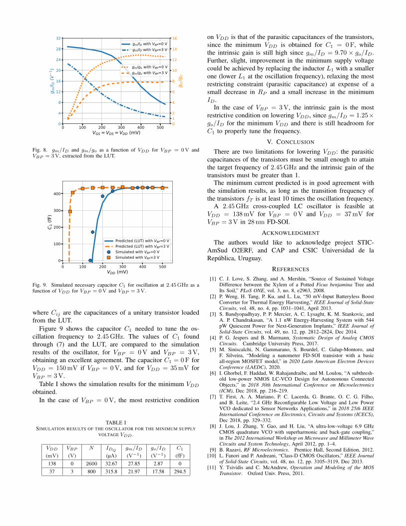
In (3), we have ID ≥ 0 if gm/ID > go/ID. This isequivalent to gm/go > 1, bounding the intrinsic gain ofthe transistor. Figure 8 shows the dependence on VDD ofgm/ID and gm/go for VBP = 0 V and VBP = 3 V. Notethat gm/go > 1 for VDD ≥ 25 mV if VBP = 0 V and forVDD ≥ 30.7 mV if VBP = 3 V.
For values of VDD for which gm/go > 1, there is an N largeenough to satisfy (5). However, increasing N increases theparasitic capacitances of the transistors. This is a problem ifthe equivalent parasitic capacitance is greater than Ctot, where
Ctot =1
(2πfosc)2L1
, (6)
because in this case the desired oscillation frequency cannotbe tuned by means of adjusting C1. Thus,
C1 = Ctot −N(
Cgs+Cgb+Csd+Cbd
2 + 2Cgd
)≥ 0, (7)
0 100 200 300 400 500VGS = VDS = VDD (mV)
0
4
8
12
16
20
24
28
32
g m/I D
(V1 )
gm/ID with VBP=0 Vgm/ID with VBP=3 V
012
4
6
8
10
12
14
16
g m/g
o
gm/go with VBP=0 Vgm/go with VBP=3 V
Fig. 8. gm/ID and gm/go as a function of VDD for VBP = 0V andVBP = 3V, extracted from the LUT.
0 100 200 300 400 500VDD (mV)
0
100
200
300
400
C 1 (f
F)
Predicted (LUT) with VBP=0 VPredicted (LUT) with VBP=3 VSimulated with VBP=0 VSimulated with VBP=3 V
Fig. 9. Simulated necessary capacitor C1 for oscillation at 2.45GHz as afunction of VDD for VBP = 0V and VBP = 3V.
where Cij are the capacitances of a unitary transistor loadedfrom the LUT.
Figure 9 shows the capacitor C1 needed to tune the os-cillation frequency to 2.45 GHz. The values of C1 foundthrough (7) and the LUT, are compared to the simulationresults of the oscillator, for VBP = 0 V and VBP = 3 V,obtaining an excellent agreement. The capacitor C1 = 0 F forVDD = 150 mV if VBP = 0 V, and for VDD = 35 mV forVBP = 3 V.
Table I shows the simulation results for the minimum VDD
obtained.In the case of VBP = 0 V, the most restrictive condition
TABLE ISIMULATION RESULTS OF THE OSCILLATOR FOR THE MINIMUM SUPPLY
VOLTAGE VDD .
VDD VBP N IDQgm/ID go/ID C1
(mV) (V) (µA) (V−1) (V−1) (fF)138 0 2600 32.67 27.85 2.87 037 3 800 315.8 21.97 17.58 294.5
on VDD is that of the parasitic capacitances of the transistors,since the minimum VDD is obtained for C1 = 0 F, whilethe intrinsic gain is still high since gm/ID = 9.70 × go/ID.Further, slight, improvement in the minimum supply voltagecould be achieved by replacing the inductor L1 with a smallerone (lower L1 at the oscillation frequency), relaxing the mostrestricting constraint (parasitic capacitance) at expense of asmall decrease in RP and a small increase in the minimumID.
In the case of VBP = 3 V, the intrinsic gain is the mostrestrictive condition on lowering VDD, since gm/ID = 1.25×go/ID for the minimum VDD and there is still headroom forC1 to properly tune the frequency.
V. CONCLUSION
There are two limitations for lowering VDD: the parasiticcapacitances of the transistors must be small enough to attainthe target frequency of 2.45 GHz and the intrinsic gain of thetransistors must be greater than 1.
The minimum current predicted is in good agreement withthe simulation results, as long as the transition frequency ofthe transistors fT is at least 10 times the oscillation frequency.
A 2.45 GHz cross-coupled LC oscillator is feasible atVDD = 138 mV for VBP = 0 V and VDD = 37 mV forVBP = 3 V in 28 nm FD-SOI.
ACKNOWLEDGMENT
The authors would like to acknowledge project STIC-AmSud O2ERF, and CAP and CSIC Universidad de laRepublica, Uruguay.
REFERENCES
[1] C. J. Love, S. Zhang, and A. Mershin, “Source of Sustained VoltageDifference between the Xylem of a Potted Ficus benjamina Tree andIts Soil,” PLoS ONE, vol. 3, no. 8, e2963, 2008.
[2] P. Weng, H. Tang, P. Ku, and L. Lu, “50 mV-Input Batteryless BoostConverter for Thermal Energy Harvesting,” IEEE Journal of Solid-StateCircuits, vol. 48, no. 4, pp. 1031–1041, April 2013.
[3] S. Bandyopadhyay, P. P. Mercier, A. C. Lysaght, K. M. Stankovic, andA. P. Chandrakasan, “A 1.1 nW Energy-Harvesting System with 544pW Quiescent Power for Next-Generation Implants,” IEEE Journal ofSolid-State Circuits, vol. 49, no. 12, pp. 2812–2824, Dec 2014.
[4] P. G. Jespers and B. Murmann, Systematic Design of Analog CMOSCircuits. Cambridge University Press, 2017.
[5] M. Siniscalchi, N. Gammarano, S. Bourdel, C. Galup-Montoro, andF. Silveira, “Modeling a nanometer FD-SOI transistor with a basicall-region MOSFET model,” in 2020 Latin American Electron DevicesConference (LAEDC), 2020.
[6] I. Ghorbel, F. Haddad, W. Rahajandraibe, and M. Loulou, “A subthresh-old low-power NMOS LC-VCO Design for Autonomous ConnectedObjects,” in 2018 30th International Conference on Microelectronics(ICM), Dec 2018, pp. 216–219.
[7] T. First, A. A. Mariano, P. C. Lacerda, G. Brante, O. C. G. Filho,and B. Leite, “2.4 GHz Reconfigurable Low Voltage and Low PowerVCO dedicated to Sensor Networks Applications,” in 2018 25th IEEEInternational Conference on Electronics, Circuits and Systems (ICECS),Dec 2018, pp. 329–332.
[8] J. Lou, J. Zhang, Y. Gao, and H. Liu, “A ultra-low-voltage 6.9 GHzCMOS quadrature VCO with superharmonic and back-gate coupling,”in The 2012 International Workshop on Microwave and Millimeter WaveCircuits and System Technology, April 2012, pp. 1–4.
[9] B. Razavi, RF Microelectronics. Prentice Hall, Second Edition, 2012.[10] L. Fanori and P. Andreani, “Class-D CMOS Oscillators,” IEEE Journal
of Solid-State Circuits, vol. 48, no. 12, pp. 3105–3119, Dec 2013.[11] Y. Tsividis and C. McAndrew, Operation and Modeling of the MOS
Transistor. Oxford Univ. Press, 2011.


![Two Novel Multiband Centimetre-Wave Patch …patch textile antenna at 2.45 GHz. A dual band tag antenna at 2.45 GHz and 5.8 GHz is proposed in [22]. A compact dual band antenna operating](https://img.pdfslide.us/doc/110x75/5fb6ae8bd8a49b714e202e9c/two-novel-multiband-centimetre-wave-patch-patch-textile-antenna-at-245-ghz-a-dual.jpg)