Embed Size (px)
Citation preview

Minimalist Analog-to-Digital Converter Structures
March 2nd, 2012School of EECS
Oregon State University
Allen Waters

Presentation Outline
• Motivation• Minimalist Quantizers• Techniques to Improve Resolution• Automating Analog Design• Proposed Structure• Conclusions
Allen Waters 2012-03-02 2

Motivation: Process Scaling
Digital circuits:+Faster+Denser+Port rapidly
Analog circuits:−Lower gmro intrinsic gain−More variability−Reduced headroom−Porting is tedious
Allen Waters 2012-03-02 3
• How can ADCs keep up with digital circuits?– Need architecture that is immune to analog component mismatch
and variations– Minimalism sacrifices performance to improve portability and scaling– Ideally, would include in existing digital synthesis and place-and-
route toolchain

Presentation Outline
• Motivation• Minimalist Quantizers• Techniques to Improve Resolution• Automating Analog Design• Proposed Structure• Conclusions
Allen Waters 2012-03-02 4

Generic Flash Quantizer• Increasing resolution is expensive
– Require k = 2N-1 comparators for N-bit resolution
• Requires analog references– Matching requirements for reference
ladder• As processes scale, Vdd decreases and
deviation in comparator offset increases– Higher probability of metastability [1]– Degrades linearity– Possible non-monotonicity [2]
Allen Waters 2012-03-02 5
Scales poorly with both resolution and process

Minimalist Flash Design• 3-level flash sacrifices
resolution for other benefits+ Minimal hardware+ Reduced probability of
metastability+ Corresponding 3-level
DAC simply switches among Vdd, Vss, Vcm; no added references
± Need analog references, but only 2 of them
Allen Waters 2012-03-02 6
How to avoid providing voltage references?

Flash with Time-Domain Comparator
Allen Waters 2012-03-02 7
• Single voltage comparator• Compare elapsed time
before comparator resolves against reference time delay+ No reference voltage+ Accounts for
metastability+ Offset in voltage
comparator can be tolerated
[3]

Flash with Time-Domain Comparator
Allen Waters 2012-03-02 8
No more minimal than 3-level flash
• Single voltage comparator• Compare elapsed time
before comparator resolves against reference time delay+ No reference voltage+ Accounts for
metastability+ Offset in voltage
comparator can be tolerated
– Now need to provide time delay reference [3]

Flash with Built-In Reference Voltage
Allen Waters 2012-03-02 9
• Intentionally size input transistors differently
• Creates a built-in comparator offset+ Removes reference ladder+ Removes differential input
pair & branch current• Can add resolution using
2nd comparator cell

VCO-Based Quantizer
Allen Waters 2012-03-02 10
• Input voltage determines time delay of inverters (VTC)
• Count inverter transitions occurring within fixed clock period (TDC)+ Highly digital+ Inherent 1st-order noise shaping+ Implicit barrel shifting and DEM– VTC has poor linearity
[4,5]

Integrating Quantizer• Sample input voltage onto
feedback capacitor• Apply constant discharging
current until capacitor voltage is reaches zero (VTC)
• Count fixed clock periods occurring within variable discharging time (TDC)+ Inherent 1st-order noise shaping+ Residue available as both voltage
and time-domain signal– Requires opamp for integrator
Allen Waters 2012-03-02 11
[6]

Minimalist Opamp Design
For minimalist design:•Single-stage amplifier•No cascoding (preserve headroom for low-voltage processes)
Allen Waters 2012-03-02 12

Integrating Quantizer without Opamp
Allen Waters2012-03-02 13
[8]
• Single sampling capacitor and discharging current source+ Avoids using opamp+ Residue available as both voltage*
and time-domain signal– Lose noise shaping– Linearity requirements on current
source
*if current source remains linear

Summary of Minimalist Quantizers
• Flash with built-in referencesFast and simple, but low resolution
• VCO-based quantizerHighly digital, but nonlinear
• Integrating quantizerResidue voltage/time available, but
relies on analog component matchingFirst-order noise shaping with opamp
Allen Waters 2012-03-02 14
Improve resolution by reducing “counting” element delay

Presentation Outline
• Motivation• Minimalist Quantizers• Techniques to Improve Resolution• Automating Analog Design• Proposed Structure• Conclusions
Allen Waters 2012-03-02 15
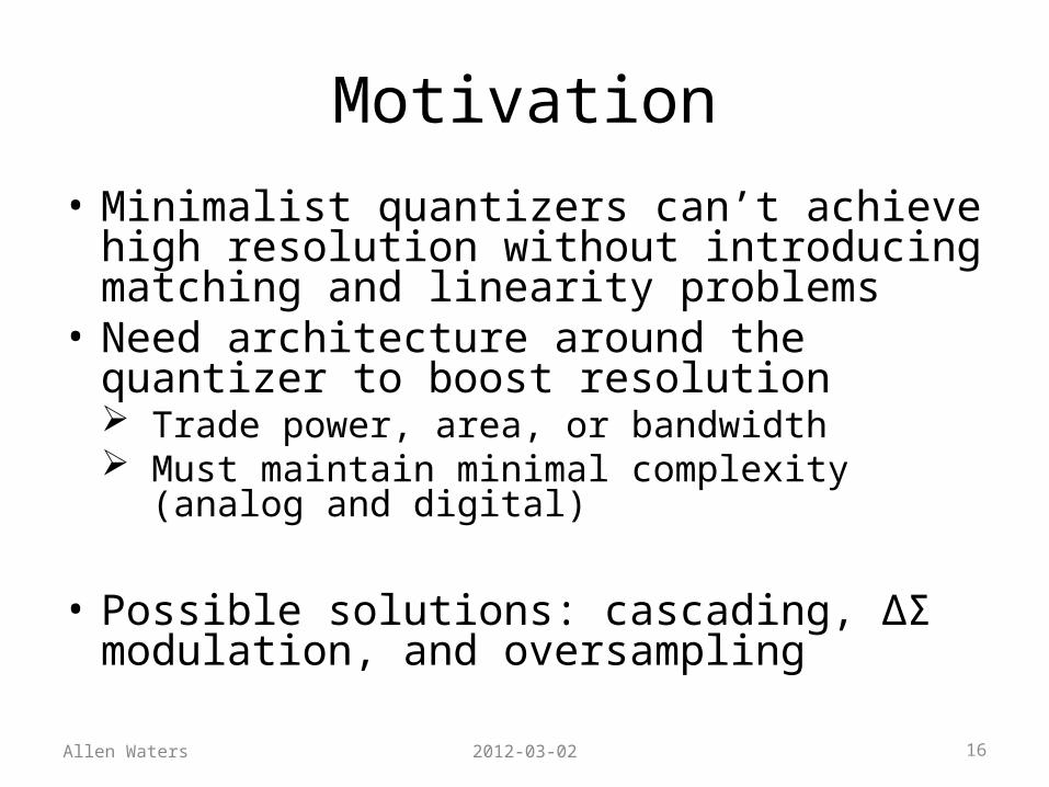
Motivation• Minimalist quantizers can’t achieve high
resolution without introducing matching and linearity problems
• Need architecture around the quantizer to boost resolution Trade power, area, or bandwidth Must maintain minimal complexity (analog and
digital)
• Possible solutions: cascading, ΔΣ modulation, and oversampling
Allen Waters 2012-03-02 16

Pipelined ADCs
• Many low-resolution stages; amplifies quantization error+ Exchanges
power/area for resolution
+ Maintains throughput
Allen Waters 2012-03-02 17
[9-11]

Pipelined ADCs
• Many low-resolution stages; amplifies quantization error+ Exchanges
power/area for resolution
+ Maintains throughput– Requires k opamps– Calibration methods
are cumbersome, many error terms
Allen Waters 2012-03-02 18
Too much analog matching and digital calibration
[9-11]

Algorithmic ADCs• More minimalist variation of pipelining• Time-share a single stage, performing k subconversions
+ Power/area reduced by k– Throughput reduced by k± Requires opamp (but only 2)+ Same gain error / variation in each stage simplifies
calibration
Allen Waters 2012-03-02 19

Introduction to ΔΣ Modulation• Feedback subtracts output
from input• Error is low-pass filtered by H• Differentiating Q suppresses it
at small frequencies Oversampling makes signal
band very small relative to sampling frequency
In-band noise strongly attenuated
Can improve resolution by increasing filter order, OSR, or number of quantizer levels
Allen Waters 2012-03-02 20
[12]

Minimalist ΔΣ Modulation• With low-performance
opamps, restrict to first-order modulators
• Add feedforward path such that loop filter only processes error, not input signal Reduces requirements for
loop filter linearity• Process residue with another
stage Multi-stAge noise SHaping
(MASH) Higher order noise shaping
without stability concerns
Allen Waters 2012-03-02 21
Requires digital filter to recombine different stage outputs
[13]

ΔΣ with VCO-Based Quantizer
Allen Waters 2012-03-02 22
• Compare VCO phase to previous state (1-z-1)
• Quantizer output is frequency+ Feedback and gain stage
predistort tuning voltage to improve linearity
– Need full range of tuning voltage to achieve all possible outputs
– Still limited by VTC nonlinearity

ΔΣ with VCO-Based Quantizer
Allen Waters 2012-03-02 23
• Compare VCO phase to reference phase [1]
• Quantizer output is phase+ Feedback holds tuning
voltage constant+ Achieves all possible output
states+ Unaffected by VTC
nonlinearity
• Compare VCO phase to previous state (1-z-1)
• Quantizer output is frequency+ Feedback and gain stage
predistort tuning voltage to improve linearity
– Need full range of tuning voltage to achieve all possible outputs
– Still limited by VTC nonlinearity

ΔΣ with Integrating Quantizer
• (2nd-order loop filter) + (1st-order noise shaping in quantizer) = (3rd-order noise shaping total)
• Although ΔΣ typically uses flash, there are benefits to using other quantizers
Allen Waters 2012-03-02 24
[7]

Stochastic Conversion• Previous methods focus on
immunity to variations in analog componentsExample: comparator
offset voltage Vos
• Using k 1-bit comparators: For large k, Vos distributed
with Gaussian PDFVin sweep gives Gaussian
CDFCorrected with inverse
Gaussian DSP function
Allen Waters 2012-03-02 25
[14]

Stochastic Conversion
Allen Waters 2012-03-02 26
+High-speed+ Low analog complexity
(synthesizable)− High-power (k
comparators)− Scales poorly: k = 4N
[14]

Summary of Minimalist Techniques
Allen Waters 2012-03-02 27
• ΔΣ Modulation (speed for resolution)– Noise-shaping and oversampling improve
performance even with low-quality analog components
• Stochastic (power/area for resolution)– Uses matching variations to improve accuracy
• Algorithmic (speed for resolution)– Will require calibration, just not as bad as pipelined
ADC• Pipelining (power/area for resolution)– Performance relies heavily on high-gain opamps
and complicated background calibration

Presentation Outline
• Motivation• Minimalist Quantizers• Techniques to Improve Resolution• Automating Analog Design• Proposed Structure• Conclusions
Allen Waters 2012-03-02 28

Analog Cell Synthesis
• Tools exist to automate analog cell design (opamps, band-gap reference, etc.) Select topology Size and bias devices Verify performance over operating variations
• Results only as accurate as specifications from designer Will be entirely different with each process
• Still perform layout by hand
Allen Waters 2012-03-02 29
[15]

Analog Cell Synthesis
• Instead, automate system layout– Using minimalist design, system architecture
won’t change much between processes– Few analog components to layout in new process– System layout automatically generated from
individual cell layouts
Allen Waters 2012-03-02 30

ADC Design Using Digital Tools• For fundamental analog building
blocks:– Manually create layout (*.gds)
and connectivity information (*.lef)
• Include these custom cells in Verilog file– Digital synthesizer ignores them– Place-and-route: places layers in
*.gds, routes to pins in *.lef• Want control over routing
among analog components– Can use timing information or
Verilog macros
Allen Waters 2012-03-02 31
[14]

Presentation Outline
• Motivation• Minimalist Quantizers• Techniques to Improve Resolution• Automating Analog Design• Proposed Structure• Conclusions
Allen Waters 2012-03-02 32

Equivalent Stochastic ADCs
• Sampling k comparators 1 time vs. sampling 1 comparator k times (proposed)
• Comparator input noise distributes Vthreshold with Gaussian PDF
Allen Waters 2012-03-02 33

Oversampled Noisy Comparator
• Oversamples in time-domain, rather than in “area-domain” like previously discussed stochastic ADC+ Highly digital+ Low complexity+ Low power– Very slow (k = 4N for N-bit resolution)– Very small input range, determined by σ of input-referred
comparator noise
• Could be appropriate for passive DC sensors+ No need to amplify sensor output
Allen Waters 2012-03-02 34

Why Does Resolution Scale So Poorly?
Allen Waters 2012-03-02 35
Slope > 1 causes lost codes in output
k = 4N
•DSP uses piece-wise linear correction function•Linear region of CDF => 1x slope•Tail regions with higher slopes skip output codes

Ideal Input Noise Distribution
• If noise could be uniformly distributed, looks like a k-level flash+ Now scales as k = 2N + Since CDF is linear, don’t need DSP correction– But uniformly-distributed noise is implausible
Allen Waters 2012-03-02 36

Creating Uniformly Distributed Region
• Two comparators, with ±σ offsets [14]
• Middle half approaches a linear distribution
Allen Waters 2012-03-02 37

Creating Uniformly Distributed Region
Allen Waters 2012-03-02 38
+ Constrain input range to more linear region− Half of comparator decisions are worthless, because
input-referred noise is greater than input range+ 2x samples / clock cycle
always 0always 1
input range

Tradeoffs in Proposed Design• Proposed single-comparator stochastic ADC using input-referred
comparator noise to resolve signal+ Highly digital (synthesizable)+ Low complexity+ Low power/area– Extremely slow
• Two-comparator implementation+ Increases speed exponentially+ DSP correction function is more simple– Requires comparator offset to be adjusted extremely accurately, on
the same order of magnitude as the comparator noise σ
• Possible performance improvements Create noise source that is nearly linear Add feedback for noise shaping
Allen Waters 2012-03-02 39

Presentation Outline
• Motivation• Minimalist Quantizers• Techniques to Improve Resolution• Automating Analog Design• Proposed Structure• Conclusions
Allen Waters 2012-03-02 40

Conclusions
• Analog circuit scaling lags behind digital• Need minimalist ADC structures that are immune
to component mismatch and variation– Minimalist quantizers achieve low resolution– Use oversampling, cascading and noise-shaping to
boost resolution at expense of speed/power• If resistant to routing variations, analog cells
could be included in existing digital design flow• Proposed a new stochastic ADC that oversamples
input-referred noise to resolve signal
Allen Waters 2012-03-02 41

References[1] M. Park and M. Perrott, “A 78 dB SNDR 87 mW 20 MHz Bandwidth Continuous-Time ΔΣ ADC With
VCO-Based Integrator and Quantizer Implemented in 0.13 μm CMOS,” IEEE J. Solid-State Circuits, vol. 44, no. 12, pp. 3344–3358, Dec. 2009.
[2] S. Weaver, B. Hershberg, P.K. Hanumolu, and U. Moon, “A Multiplexer-Based Digital Passive Linear Counter (PLINCO),” in Proc. IEEE Int. Conf. on Electronics, Circuits and Syst., 2009, pp. 607–610.
[3] J. Guerber, M. Gande, H. Venkatram, A. Waters, and U. Moon, “A 10b Ternary SAR ADC with Decision Time Quantization Based Redundancy,” in Proc. IEEE Asian Solid-State Circuits Conf., 2011, pp. 65–68.
[4] M. Straayer and M. Perrott, “A 12-Bit, 10-MHz Bandwidth, Continuous-Time ΔΣ ADC With a 5-Bit, 950-MS/s VCO-Based Quantizer,” IEEE J. Solid-State Circuits, vol. 43, no. 4, pp. 805–814, Apr. 2008.
[5] ——, “A Multi-Path Gated Ring Oscillator TDC With First-Order Noise Shaping,” IEEE J. Solid-State Circuits, vol. 44, no. 4, pp. 1089–1098, Apr. 2009.
[6] N. Maghari, G.C. Temes, and U. Moon, “Noise-shaped integrating quantisers in ΔΣ modulators,” IET Electron. Lett., vol. 45, no. 12, pp. 612–613, June 2009.
[7] N. Maghari and U. Moon, “A Third-Order DT ΔΣ Modulator Using Noise-Shaped Bi-Directional Single-Slope Quantizer,” IEEE J. Solid-State Circuits, vol. 46, no. 12, pp. 2882–2891, Dec. 2011.
[8] M. Park and M.H. Perrott, “A Single-Slope 80MS/s ADC using Two-Step Time-to-Digital Conversion,” in Proc. IEEE Int. Symp. on Circuits and Syst., 2009, pp. 1125–1128.
Allen Waters 2012-03-02 42

References[9] C.R. Grace, P.J. Hurst, and S.H. Lewis, “A 12-bit 80-MSample/s Pipelined ADC With Bootstrapped
Digital Calibration,” IEEE J. Solid-State Circuits, vol. 40, no. 5, pp. 1038–1046, May 2005.[10] I. Galton, “Digital Cancellation of D/A Converter Noise in Pipelined A/D Converters,” IEEE Trans.
Circuits Syst. II, vol. 47, no. 3, pp. 185–196, Mar. 2000.[11] H. Liu, Z. Lee, and J.Wu, “A 15-b 40-MS/s CMOS Pipelined Analog-to-Digital Converter With Digital
Background Calibration,” IEEE J. Solid-State Circuits, vol. 40, no. 5, pp. 1047–1056, May 2005.[12] B. Boser and B. Wooley, “The Design of Sigma-Delta Modulation Analog-to-Digital Converters,”
IEEE J. Solid-State Circuits, vol. 23, no. 6, pp. 1298–1308, Dec. 1988.[13] R. Schreier and G. Temes, Understanding Delta-Sigma Data Converters, 1st ed. Hoboken, NJ: John
Wiley and Sons, Inc, 2005.[14] S. Weaver, “Automated Synthesis of Analog to Digital Conversion,” Ph.D. dissertation, Oregon State
University, 2010.[15] E.S. Ochotta, T. Mukherjee, R.A. Rutenbar, and L.R. Carley, Practical Synthesis of High-Performance
Analog Circuits, 1st ed. Norwell, MA: Kluwer Academic, 1998.
Allen Waters 2012-03-02 43

Barrel Shifting and DEM
• Delay cell transitions resume where previous cycle left off– Barrel shift through delay cells shapes the td mismatch– Using phase output from XOR gates, also get dynamic element
matching (DEM) of DAC elements to shape mismatch
Allen Waters 2012-03-02 44

Example Cell Design and Usage
MACRO unitC ORIGIN 0.00 0.00 ; SIZE 14.52 BY 15.12 ; PIN A DIRECTION INOUT ; PORT LAYER metal5 ; RECT 2.91 3.21 11.61 11.91 ; END END A PIN B ... END B PIN VDD ... END VDD PIN VSS ... END VSS OBS ... ENDEND unitC
Allen Waters 2012-03-02 45
...module myModule(input X, output Y); supply1 VDD; supply0 VSS;
... unitC C1( .A(X), .B(VSS) ); ...
endmodule myModule...
unitC.lefADC.v
• Placing custom cells is easy
• Controlling the routing is the challenge
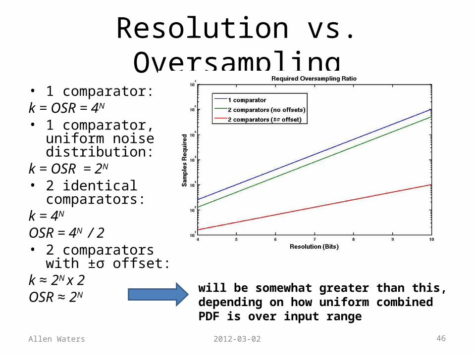
Resolution vs. Oversampling
Allen Waters 2012-03-02 46
• 1 comparator:k = OSR = 4N
• 1 comparator, uniform noise distribution:
k = OSR = 2N
• 2 identical comparators:
k = 4N
OSR = 4N / 2• 2 comparators with
±σ offset:k ≈ 2N x 2OSR ≈ 2N
will be somewhat greater than this, depending on how uniform combined PDF is over input range