Embed Size (px)
Citation preview

HF PACKER AMP miniHFPA Page 1
miniHFPA2 HF Packer Amp Construction Manual
miniHFPA2 PACKER –AMP REV 1
www.hfprojects.com [email protected] 281-467-9424 Revised 1/5/18
A new configuration of the miniHFPA HF Packer Amp with the emphasis of a new assembly paradigm to match the needs of the assembler. All of the mission-critical electronics is
preassembled and tested. The user completes the kit by bringing together the major assemblies into a finished case with less technical skills required.
The major emphasis in this design is to reduce the need for complexity in Builder efforts to do this project. As a result, we have one circuit board and no cables to fabricate. The builder has the comparatively simple task of final assembly.
The final assembly kit information is in section Five for the miniHFPA2 final assembly.
The full assembly instructions are included to be able to share the theory of operation and maintenance instructions.
Pictured here is the flat plate heat sink version which is thinner and more ergonomic for portable backpacking needs. The choice of the heat sink for the miniHFPA is an option.

HF PACKER AMP miniHFPA Page 2
Contents ............................................................................................... 1
Section One - Introduction ................................................... 5
Circuit Details ...................................................................... 6
Performance ........................................................................ 7
Terms used in the descriptions ............................................ 7
Test Header Pins ................................................................. 8
Front Panel Controls ............................................................ 8
The Inline-Bypass Switch ................................................. 8
STBY-ON Switch ............................................................. 8
CW and SSB Switch ........................................................ 8
LPF Switch ....................................................................... 8
SWR Detection, Indication and Response ........................... 9
DC Power In and Battery Power Switching .......................... 9
Over-Current Limiting Circuit ............................................... 9
miniHFPA Power Supply Timing Signals ............................. 9
PTT Operation ................................................................... 10
Preparation ........................................................................ 10
Inspection of Surface Mount Components ......................... 10
Construction Techniques ................................................... 10
Good Soldering Technique ................................................ 11
Suggested Tools ............................................................... 11
Included Speciality Tools ................................................... 11
Component Installation ...................................................... 11
Care of the IRF-510 MOSFET's ........................................ 12
Other Construction Notes.................................................. 12
Mechanical Drawings ........................................................ 13
Section Two – Amplifier Module Construction ...................... 14
Assembly Steps ................................................................ 14
Install 14 Pin Socket for U2 and Header H3 ...................... 16
Fabricated Magnetics Step By Step .................................. 21
Fabrication of T1 ............................................................... 21
Fabrication and Assembly of T2 ........................................ 22
Fabrication and Assembly of T3 ........................................ 26
Fabrication and Assembly of L1 and L3 ............................ 27
Fabrication and Assembly of L2 ........................................ 28
Fabrication and Assembly of T4 ........................................ 28
PI-Resistive Network Installation ....................................... 30
PI-Resistive Network and Bias Pots .................................. 31
Bottom Cover Assembly ................................................... 31
Heat Sink Assembly .......................................................... 32
Top Cover Assembly ......................................................... 32
Heat Sink Attachment ....................................................... 32
MOSFET Circuit Board Mounting ...................................... 33
Circuit Board Preliminary Test .......................................... 33
Bias function test .............................................................. 33
MOSFET Mounting and Bias Setting ................................ 34
Attach the Circuit board to the heat sink ........................ 35
HF PACKER AMP miniHFPA Page 3
Option Switch Guard Assembly ......................................... 37
Section Three – Adjustment and Testing............................... 38
Ohmmeter Test ................................................................. 38
Basic Current Test ............................................................. 38
DC Test and Bias Adjustment ............................................ 38
What to check if it doesn’t work ......................................... 39
Example Problem: Power LED does not light. ................ 39
Example Problem: The TX LED does not light when you jumper the TEST, H2, pins together. .............................. 39
Example Problem: The current does not increase when you turn VR1 or VR2 clockwise. ..................................... 40
Tests with Circuit Board Installed ....................................... 40
Install two LPF Modules .................................................... 40
Test Mode Setup ............................................................... 40
RF Signal Testing .............................................................. 41
Voltage Test ...................................................................... 41
LT1270ACT Alert Notice .................................................... 41
RF Power Testing .............................................................. 41
PTT Connections FLEX 1500 and FT817 .......................... 42
.......................................................................................... 43
Section Four – Specifications and Operation ........................ 45
Specifications .................................................................... 45
Operation .......................................................................... 45
Do’s and Don’ts for Successful Operation ......................... 46
Maintenance Issues .......................................................... 46
CW/SSB Selection ............................................................ 46
Theory of Operation and Troubleshooting ......................... 46
Power Supply Unit ............................................................ 46
Power Input ................................................................... 47
Reverse Voltage Protection ........................................... 47
DC-DC Converter, U4.................................................... 47
Timing Sequence of Control Signals .............................. 47
U4 Control ..................................................................... 48
Fully Protected High Side Power MOSFET Switch, U5 .. 48
CONTROL ..................................................................... 48
Big Picture ..................................................................... 48
U6 ................................................................................. 48
K2, K3, and J4 ............................................................... 48
TX Signal Generation .................................................... 49
PTT Control ................................................................... 49
CW or SSB option ......................................................... 49
TEST Jumper, H3 .......................................................... 49
5V Regulator ................................................................. 49
TX LED ......................................................................... 49
MOSFET AMP Schematic ............................................. 49
Pi-resistive Network ....................................................... 50
L2 and T3 ...................................................................... 50
T2 .................................................................................. 50

HF PACKER AMP miniHFPA Page 4
T1 .................................................................................. 50
BIAS .............................................................................. 50
BIAS Adjustment ............................................................ 50
Heat Sinking the MOSFETs ........................................... 51
Section 5 miniHFPA2 Final Assembly ................................... 52
Introduction to assembly steps .......................................... 52
Attach four panel switches ................................................. 52
Attach two RF Connectors and RCA Jack ......................... 52
Install eight guide bumpers on the circuit board ................. 52
Bottom Cover Assembly .................................................... 53
Attaching the Heat Sink Plate to the Case Top .................. 53
Apply a thin layer of thermal grease to the two ceramic washers ............................................................................. 53
Apply a thin layer of thermal grease to the heat sink plate where the ceramic washers and MOSFETs will attach ...... 54
Attach the two ceramic washers to the heat sink plate ....... 54
Attach threaded standoff spacers ...................................... 54
Attach the heat sink plate to the case with mounting hardware ........................................................................... 54
Insert the completed circuit board into the top portion of the case. ................................................................................. 54
Insert the two LPF Modules of Choice into the right-angle header connectors, J5 and J6 ........................................... 55
Attach the bottom panel to the case assembly ................... 56
Attach the side panels ....................................................... 56

HF PACKER AMP miniHFPA Page 5
Section One - Introduction Welcome, all builders to the homebrew HF Packer-
Amp miniHFPA Project. This project parts and your efforts will eventually provide you with a compact 5-watt input to 30-35 watt output linear amplifier for use with QRP SSB/CW transmitters on selected amateur bands 160 through 10 meters and powered from a 12 volt DC supply. This section, you review the building of the miniHFPA HF Packer Amp. The design is a good balance between output power, physical size and battery power consumption. The completed amplifier will reward the builder with a clean, more powerful output signal for a QRP rig when radio conditions become marginal.
This project is optimized to permit lower skilled radio amateurs to complete the project with the minimal use of special tools and test equipment. You do not need to:
• Fabricate a case and finish it. • Drill and Tap Heat Sink Threaded holes • Install Surface Mount Components • Wind and measure inductors for low pass
filters. • Make Internal Cables • Supply test equipment or tools to measure
inductance or crimp connections for cables. Your building and testing tasks include:
• Soldering through-hole components • Follow a step-by-step construction manual • Measure current when called for in the
procedure to set the bias.
• Measure Voltage to confirm the correct DC-DC Output Voltage reading.
• A dummy load, 100W 50 ohm • Your transceiver, your power source, your two
RG58 cables for RF connections.
You can take advantage of offered fabricate options available to you:
• Fabricate and install Amp circuit board Inductors and transformers.
• Through hole assembly
Builders require soldering, hand tool, basic electronics and component identification skills. This project manual is supplied by email to keep kit costs to a minimum. All builders will receive the construction manual in a PDF format. You can also download from the HF Projects store: www.hfprojects.com or from the files residing at http://groups.yahoo.com/group/hfprojects/ Membership is free. You will also have the opportunity to access the drop box for the project. You will receive the link after completing your purchase of the project. The manual is produced in landscape format to allow more readable text per screen. This manual provides all you will need to complete the amplifier project, however, some additional PDF files located at the project dropbox for those interested in seeing more pictures of the project at various stages of construction.
The genesis of the basic amp circuit is fully described in the 2001 ARRL Handbook and reprint articles from the ARRL. If you are an ARRL member, you can view the amplifier articles online. Full amplifier circuit design credits to Mike Kossor, WA2EBY. The amplifier circuit board is attached to the

HF PACKER AMP miniHFPA Page 6
top cover in a two-part chassis design. The MOSFETs are electrically isolated and attached to the heat sink by two #6 nylon cap screws. The power supply unit is an integral part of the amplifier module along with two plug-in low-pass filters (LPF) modules. Each LPF covers two adjacent band segments from 160M, 80/75M, 60/40M, 30/20M, 17/15M and 12/10M.
Circuit Details
The circuit board is a four-layer design optimized to allow logic and RF to exist in the same world. The technique used is to put the RF devices on the top layer with a ground plane directly below the top layer. The 3rd and 4th layers are for signal routing of the control system.
The amplifier module is a push-pull design, biased for Class AB linear operation and uses low-cost power MOSFETs in its output stage. Maximum efficiency is at 10 MHz and develops over 50 watts output. QRP transmitter RF input is first sensed, which trips a relay, feeding RF through an RF attenuator pad. The signal connects to the primary of T3 via an input impedance matching network consisting of L2. T3 is a 1:1 balun that splits the RF signal into two outputs 180 degrees out of phase. One of these signals connects to Q1's gate. The other signal routes to Q2's gate. The drains of Q1 and Q2 connect to the primary of output transformer T1, where the two signals are recombined in phase to produce a single output. T1 also provides an impedance transformation from the low output impedance of the MOSFETs to the 50Ω antenna port. DC power connects to the drains of Q1 and Q2
by phase-reversal choke, T2. This configuration is a design method to provide power to Q1 and Q2 while presenting a high impedance to the RF signal over a broad range of frequencies. The drain chokes for Q1 and Q2 created on the same core, and the phase of one of the chokes is the reverse. C5 increases the bandwidth of impedance transformation provided by T1, especially at 21 MHz. The 5 V bias supply voltage is the output of a 78L05 regulator. Bypass capacitors remove RF voltages from the bias supply voltage. Gate bias for Q1 and Q2 are independent adjustments. VR1 adjusts Q1's gate-bias voltage via R1 while VR2 is the control for Q2 via R2. At low frequencies, the amplifier's input impedance is essentially equal to the series value of R1 and R2. L1 and L3 improve the input impedance match at higher frequencies. The low value of series resistance provided by R1 and R2 also reduces the Q. A Resistive Pi Network (R3, R7, R8) provide a 50-ohm impedance to the transceiver and the AMP. The standard network attenuates the RF Input by 9dB which is an 8:1 power ratio. The maximum RF input of 5W reduces to 0.63W at the gates of the MOSFETs. The attenuation matches the popular FT817 power setting of 5W. The maximum drive level of 0.63W is below the distortion level of the MOSFETs for distortion-free SSB operation. The bias current is 100mA per MOSFET while transmitting. The bias current is off while in idle. Two additional sets of pi-resistive networks included for 2.5W and 1W max RF input. These additional resistive networks allow you to customize your miniHFPA max RF input to match your transceiver output. You do not want to over-drive the miniHFPA because this will result in excess drain current and destructive internal heating within the MOSFETs. The standard is the 5W pi-resistive network.
HF PACKER AMP miniHFPA Page 7
The switch-mode power supply circuits boost the
nominal 12 VDC input to 29 – 29.5 VDC at 3-4 amperes during voice peaks. The power supply is normally off unless commanded to be on by the Controller IC, U2. During receive or standby, the current is very low. There is an approximate 76 mA current draw when the power supply is off, and 295 mA current draw when the power supply is on and 3-10A current draw when a transceiver keys the miniHFPA.
Performance
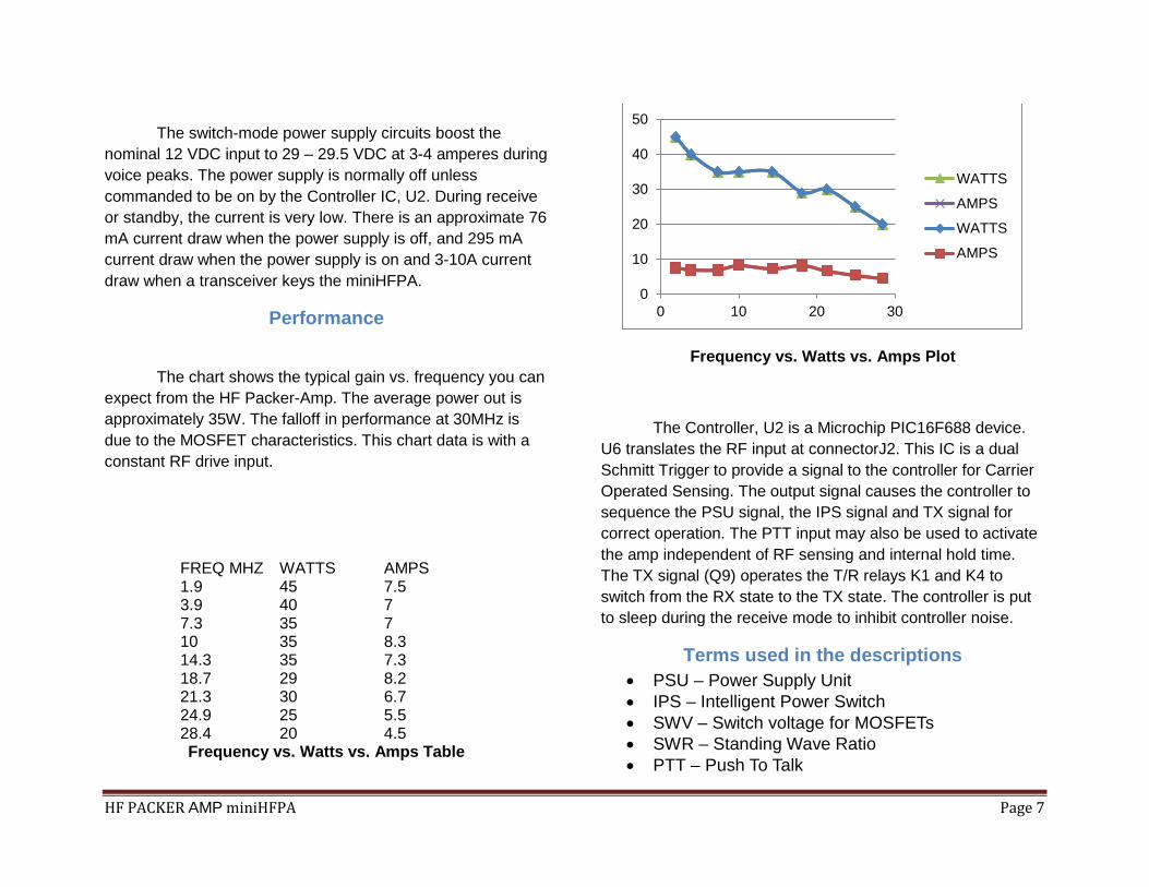
The chart shows the typical gain vs. frequency you can expect from the HF Packer-Amp. The average power out is approximately 35W. The falloff in performance at 30MHz is due to the MOSFET characteristics. This chart data is with a constant RF drive input.
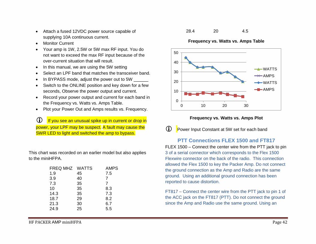
FREQ MHZ WATTS AMPS 1.9 45 7.5 3.9 40 7 7.3 35 7 10 35 8.3 14.3 35 7.3 18.7 29 8.2 21.3 30 6.7 24.9 25 5.5 28.4 20 4.5 Frequency vs. Watts vs. Amps Table
Frequency vs. Watts vs. Amps Plot
The Controller, U2 is a Microchip PIC16F688 device. U6 translates the RF input at connectorJ2. This IC is a dual Schmitt Trigger to provide a signal to the controller for Carrier Operated Sensing. The output signal causes the controller to sequence the PSU signal, the IPS signal and TX signal for correct operation. The PTT input may also be used to activate the amp independent of RF sensing and internal hold time. The TX signal (Q9) operates the T/R relays K1 and K4 to switch from the RX state to the TX state. The controller is put to sleep during the receive mode to inhibit controller noise.
Terms used in the descriptions • PSU – Power Supply Unit • IPS – Intelligent Power Switch • SWV – Switch voltage for MOSFETs • SWR – Standing Wave Ratio • PTT – Push To Talk
0
10
20
30
40
50
0 10 20 30
WATTS
AMPS
WATTS
AMPS
HF PACKER AMP miniHFPA Page 8
• AMP – Amplifier • TX - Transmit • On/Standby – TX Enable • LPF – Low Pass Filter • XCVR – Transceiver • BOM – Bill of Material • Core – Magnetic toroid material in the shape of a
donut.
The IPS signal passes the PSU voltage to the
MOSFETs through the IPS electronic switch U5. The PSU signal activates the DC-DC converter on from a standby state. The IPS device acts as a power switch and over-current sensor to protect the DC-DC converter IC, U4. The U5 device purposely heats up rapidly to provide a thermal time constant circuit breaker if the current exceeds 5A. After the U5 device cools, the circuit breaker automatically resets.
Test Header Pins A TEST header, H3, (two vertical pins) on the circuit
board marked TEST provides a means to set the bias current. A jumper plug is included to activate the bias adjustment conveniently. See the section on adjustment before jumpering the TEST header.
Front Panel Controls The Inline-Bypass Switch
The Bypass position allows the RF input to pass from the RF Input Jack to the RF output Jack effectively bypassing the miniHFPA. Power to the miniHFPA may be on or off while bypassed. The Bypass position is also the position used while
setting the bias current. The Inline position allows RF input to be amplified by the miniHFPA.
STBY-ON Switch The STBY-ON switch switches from a standby power position (very tiny current drain) to the ON position. In the ON position but not transmitting, the DC voltage connects the controller IC which orchestrates the switching of the main power to the DC-DC Converter during transmit.
CW and SSB Switch The miniHFPA has programmed a post delay (hang-time) which is selected by the CW-SSB switch. The hang-time is longer for SSB operation. The specific time delays are described later in this manual.
LPF Switch The LPF Switch selects one of the two plugged in LPF modules. A LED indicates which LPF is selected.The miniHFPA has two removable side panels on the case which allow field access to the LPF Modules. The modules slide and plug into a header strip. Each module covers two adjacent band segments. The choices are:
1. 160 M (one segment) 2. 80/75 M 3. 60/40 M 4. 30/20 M 5. 17/15 M 6. 12/10 M
The most popular LPF choices are the 60/40M and 30/20M. The LPF switch selects the active LPF and indicates by the
HF PACKER AMP miniHFPA Page 9
appropriate LED.indicator. Each LPF is uniquely identified by a connection on each LPF to light the appropriate LED on the miniHFPA panel. The modules plug-in on either side of the miniHFPA board.
SWR Detection, Indication and Response The miniHFPA incorporates an SWR detection and feedback circuit to shut down the miniHFPA transmit operation if a high SWR is detected. The reflected current through T4 is processed by the detection and filtering circuit to Q3. In the presence of a high SWR, Q3 will conduct providing a momentary signal to the controller, U2. The SWR state will tell U2 to shut down and light the SWR indicator. The amp will switch to bypass operation. To recover, the user should investigate what could have caused the high SWR. You can return to normal operation by cycling the STBY/ON switch, to STBY and then back to ON.
DC Power In and Battery Power Switching Power enters through J3 and passes through CB1, an electronic circuit breaker. If you have sustained current greater than 10A, CB1 will purposely cause the component to become hot and open circuit for a thermal time constant and thereby protect the miniHFPA from an over-current situation. A scenario which could happen if you connect the battery up backward causing a heavy current flow through D5, the reverse polarity protection circuit. The battery input current (nominal 12VDC supply) also flows through F1, a tiny thermal fuse, that allows current to flow through Q5 if the STBY/ON switch is in the ON position. The 12V on the collector of Q5 is
the source voltage for the low current circuits on the miniHFPA. In the ON position of SW3, the regulated 5V (VCC) will be the output of U1, a voltage regulator. The regulated 5V supplies the source voltage to the bias adjustment pots, VR1 and VR2. Integrated circuits, U2 and U6, are powered by this switched 5V source. In the OFF position, the standby current is less than 1mA, and all electronics are switched OFF.
Over-Current Limiting Circuit The U5 chip passes current from the DC-DC Converter circuit (29.5 VDC in TX) through the Intelligent Power Source, U5. In the event of over-current within U5, the chip will reduce the DC-DC Converter.output voltage. Sustained over-current will cause U5 to get hot and create a thermal time delay to cease the over-current situation. After the thermal time delay passes, the U5 circuit activates again. When U5 is off, the TX LED is off. The TX LED is a good troubleshooting tool to determine whether the miniHFPA is receiving the MOSFET drain supply voltage.
miniHFPA Power Supply Timing Signals The Controller Chip, U2 sequences the operation of the power supply and the availability of the MOSFET drain voltage. The described sequence below happens in real-time with a quick and determined response to not impede the operation of the miniHFPA amplifier.The sequence is:
1. The TX signal from U2 activates the T/R relay, switching the miniHFPA from receive to transmit.
2. After allowing time for the T/R relays to switch, the PSU signal is energized to power up the DC-DC

HF PACKER AMP miniHFPA Page 10
converter and present the 29.5 VDC from the output of the DC-DC Converter circuit to the input of U5, the intelligent power switch.
3. The IPS signal from U5 passes the SWV present at the OUTPUT of U5 to the amp circuit transformer, T2.
4. The SWV is now present at the transformer T2 to supply the voltage requirement for the Q1 and Q2 drains.
5. Upon cessation of the transmit signal, a reverse sequence occurs allowing the miniHFPA to transition from Transmit to Receive.
PTT Operation The miniHFPA can be controlled and driven by the transceiver directly from the Push-To-Talk circuits of the transceiver. PTT will bypass the RF Carrier detect circuits of the miniHFPA. The same internal timing sequences are valid, but there is no hang-time delay involvement. The PTT input from the transceiver operates U3 which is a control input on U2. The time delays are now a function of the settings on the transceiver.
Preparation The most important preparation step before building is to read this section of the manual. The descriptions will familiarize you with the circuitry, the building requirements, and the components.
After reading this document and before assembly you should do an inventory of parts. In the unlikely event that you appear to have missing parts, duplicates or wrong parts please first double check for the parts in all bags, recheck the
inventory and contact Virgil via email or phone if you have a question.
Inspection of Surface Mount Components
The circuit board back side has all the surface mount parts pre-installed by machine and by hand. We have some early experience where certain resistors are soldered on one end only. In particular, R31 and R32 have been spotted with solder on one end only. For this reason, it would be a good idea to spend a few minutes inspecting the surface mount parts under a light with a magnifier making sure that the surface mount parts have solder on each end.
Construction Techniques
It is a fact that 90-95% of problems with completed electronics/radio kits are due to either component misplacement or soldering faults. We cannot stress highly enough the importance of double checking component installation before soldering and then good soldering technique to have a working amplifier at the end of this project. Other builder faults are active component damage due to overheating and damage to circuit board pads and tracks caused by poor de-soldering, too high a wattage of soldering iron or carelessness. It is very rare to have initially faulty components or printed circuit boards (PCBs).

HF PACKER AMP miniHFPA Page 11
Good Soldering Technique use a 12-25 watt soldering iron with a clean, non-
corroded, well-wetted, fine tip keep the tip clean by frequently rubbing it with a wet
sponge keep the tip tinned ensure the soldering iron tip is at its working
temperature and is in contact simultaneously with both surfaces to be soldered (the pad and the component)
let the contact zones heat before applying only electronics grade rosin cored solder (usually 3-6 seconds will do)
apply the solder to the two surfaces (not the iron tip) and only enough solder to coat both surfaces
ensure that the joint does not move after you remove the soldering iron tip and until the solder has solidified
the resultant good solder joint should be shiny, in perfect contact with pad and wire and often has a concave upwards appearance
Toroids and inductors you will wind and solder in this project use enamel coated magnet wire. The enameled wire used is designed to be stripped by a soldering iron at 750 deg F. This makes it much easier to tin the wire before insertion into the circuit board holes. The project provides two sizes of magnetic wire #22 AWG (thickest), 24 AWG (thinnest).
Suggested Tools
12-25 watt electronics soldering iron, electronics grade solder, iron stand and sponge. You might want a small iron
socket for tiny joints and a larger wattage iron when soldering to a ground plane.
De-soldering braid and desoldering pump or bulb fine needle nose pliers, small fine wire cutters, wire stripper small screwdrivers including jewelers screwdrivers, small
file multimeter Higher wattage soldering iron. I recommend a Weller
WES51 which has nice features.
Included Speciality Tools
7/64 Hex Head tool
Component Installation
For each component, our word “Install” always means:
Pick the correct part to start the Assembly notes that follow we often provide a part number only. You must match this part number with the correct component using the BOM.
Insert the component into the correct PCB position. Refer to the PCB component outline (silkscreen). Orient it correctly, following the PC board outline. Orientation is vital for active components, electrolytic and tantalum capacitors and diodes. Also, it is good practice to mount resistors and capacitors in identical orientations (for resistors normally read color code left to right in the same direction as the silkscreen on the PC board). Uniformity makes component checks easier.

HF PACKER AMP miniHFPA Page 12
Arrange the resistors on the table before you from left to right with the lowest values on the left progressing to higher values on the right. Use the multimeter to confirm the resistor values.
Install all low profile components first: usually resistors, capacitors, diodes, then electrolytic capacitors and active components.
Resistors should mount flush to the board. Mount all capacitors, relays and connectors as flush to the
board as possible. Bend the wires of the components at the bottom side
slightly outwards to hold the component in place for soldering.
Solder as per techniques described above. Flush cut excess wire leads and reflow the solder
connection for assurance and a better-looking solder joint.
Mark off each installation step in sequence as you complete it, in the box provided (e.g. ).
Warnings and important points marked with a symbol.
Care of the IRF-510 MOSFET's
MOSFETs are susceptible to electrostatic discharge damage (ESD). It is important to use proper grounding techniques while handling the amp circuit board and the MOSFETs in particular. While working with MOSFETs, you should wear a grounding strap and have an antistatic mat at your feet. At the very least you should frequently ground your
hands to the nearest ground point. The IRF510 is a good compromise MOSFET that will work up to 30 MHz but has poor thermal characteristics of 3.5°C/Watt. When used in intermittent SSB and CW service forced-air cooling is not required. Tuning time with full power should be limited to less than 120 seconds with 60 seconds between cycles to prevent overheating. Operating at 29.5 VDC does not press the MOSFET to their limits. The ceramic washer TO220 mounting kit has excellent thermal performance and provides a robust thermal interface between the MOSFET and the heatsink. The attachment cap head screws are 6-32 nylon Users report that this amplifier can safely operate for contest CW operation without further cooling. For PSK/RTTY consider an external fan or reduce the input drive.
Other Construction Notes
1. Follow the sequence given to locate the next component in a series to install.
2. The header parts, J5 and J6, require proper alignment to allow the LPF modules inserted without alignment issues. To place the headers at the proper height, slide a small slip of paper between the connector body and the circuit board. Start by soldering one pin and then while reheating, align the part flush and perpendicular to the board. Solder the remaining pins.
3. The IPS511S, U5 component is pre-mounted since it is a surface mount part.
4. The reference numbers used are not in numerical order, and some reference numbers may skip.
HF PACKER AMP miniHFPA Page 13
5. The circuit boards should receive cleaning after soldering to remove solder flux residue. I recommend “TechSpray BLUE SHOWER” available in a can: 1630-16S. Use in a ventilated area following instructions on the can or alcohol and Q-tips or a combination.
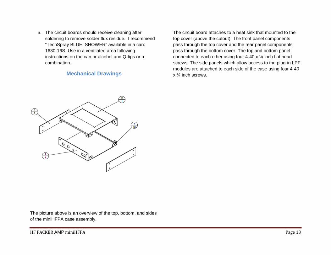
Mechanical Drawings
The picture above is an overview of the top, bottom, and sides of the miniHFPA case assembly.
The circuit board attaches to a heat sink that mounted to the top cover (above the cutout). The front panel components pass through the top cover and the rear panel components pass through the bottom cover. The top and bottom panel connected to each other using four 4-40 x ¼ inch flat head screws. The side panels which allow access to the plug-in LPF modules are attached to each side of the case using four 4-40 x ¼ inch screws.
HF PACKER AMP miniHFPA Page 14
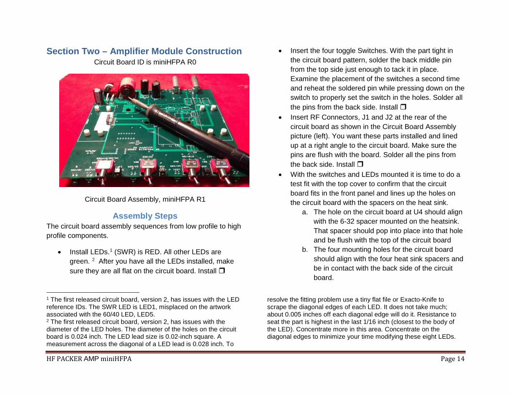
Section Two – Amplifier Module Construction Circuit Board ID is miniHFPA R0
Circuit Board Assembly, miniHFPA R1
Assembly Steps The circuit board assembly sequences from low profile to high profile components.
• Install LEDs.1 (SWR) is RED. All other LEDs are green. 2 After you have all the LEDs installed, make sure they are all flat on the circuit board. Install
1 The first released circuit board, version 2, has issues with the LED reference IDs. The SWR LED is LED1, misplaced on the artwork associated with the 60/40 LED, LED5. 2 The first released circuit board, version 2, has issues with the diameter of the LED holes. The diameter of the holes on the circuit board is 0.024 inch. The LED lead size is 0.02-inch square. A measurement across the diagonal of a LED lead is 0.028 inch. To
• Insert the four toggle Switches. With the part tight in the circuit board pattern, solder the back middle pin from the top side just enough to tack it in place. Examine the placement of the switches a second time and reheat the soldered pin while pressing down on the switch to properly set the switch in the holes. Solder all the pins from the back side. Install
• Insert RF Connectors, J1 and J2 at the rear of the circuit board as shown in the Circuit Board Assembly picture (left). You want these parts installed and lined up at a right angle to the circuit board. Make sure the pins are flush with the board. Solder all the pins from the back side. Install
• With the switches and LEDs mounted it is time to do a test fit with the top cover to confirm that the circuit board fits in the front panel and lines up the holes on the circuit board with the spacers on the heat sink.
a. The hole on the circuit board at U4 should align with the 6-32 spacer mounted on the heatsink. That spacer should pop into place into that hole and be flush with the top of the circuit board
b. The four mounting holes for the circuit board should align with the four heat sink spacers and be in contact with the back side of the circuit board.
resolve the fitting problem use a tiny flat file or Exacto-Knife to scrape the diagonal edges of each LED. It does not take much; about 0.005 inches off each diagonal edge will do it. Resistance to seat the part is highest in the last 1/16 inch (closest to the body of the LED). Concentrate more in this area. Concentrate on the diagonal edges to minimize your time modifying these eight LEDs.
HF PACKER AMP miniHFPA Page 15
c. If you are having some registration problems, make certain that the LEDs are not binding and causing the board to fit improperly in the front panel holes. Try loosening the four 4-40 screws attaching the heat sink to the top cover panel.
d. The assemblies are precisely drilled however the heatsink hole positions may vary slightly.
• Attach the eight nylon spacers with eight 4-40 screws to provide bumpers to help guide the Low-Pass Filters into place on the amp board.
• You will need to grip the spacer with your hand tool pliers while screwing the silver color 4-40 self-tapping screws into the nylon.
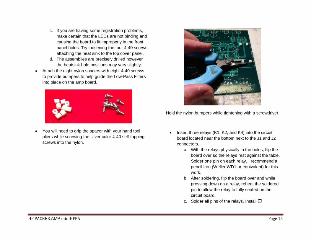
Hold the nylon bumpers while tightening with a screwdriver.
• Insert three relays (K1, K2, and K4) into the circuit board located near the bottom next to the J1 and J2 connectors.
a. With the relays physically in the holes, flip the board over so the relays rest against the table. Solder one pin on each relay. I recommend a pencil iron (Weller WD1 or equivalent) for this work.
b. After soldering, flip the board over and while pressing down on a relay, reheat the soldered pin to allow the relay to fully seated on the circuit board.
c. Solder all pins of the relays. Install
HF PACKER AMP miniHFPA Page 16
• Install relay K3 on the circuit board and repeat the soldering steps above. Install
• Locate J4, the right angle PC mount RCA Jack. This copper color connector has five tabs like connections that insert from the top side of the circuit board into the J4 location on the board. On the reverse side, bend the tabs outward slightly to hold the component in the board flush against the circuit board. When you solder the five connections, it is not necessary to fill the tab holes completely with solder. After installation and inspection, clip the excess lead length of the mechanical tabs. Install
• Locate the right-angled 10-pin headers that get installed into J5 and J6. Cut a slip of paper about a ½ x ½ inch and slide the paper between the connector and the circuit board. The paper acts as a spacer to properly set the height of J5 and J6 above the circuit board.
• In addition to being the right height, you need to make certain that the pins are parallel to the circuit board surface. To do this:
a. Tack solder a corner pin on the top side. b. Eye-ball the pins to be certain the pins are
parallel to the surface of the board. Reheat the tacked joint while making any necessary adjustments to the connector.
c. Insert an LPF Module to aid you in alignment evaluation.
d. Repeat alignment for both J5 and J6. e. Solder all the pins from the back side using a
pencil iron.
f. Remove the paper spacers after soldering. g. Remove the LPF module and save for later.
Install 14 Pin Socket for U2 and Header H3 • Flip the circuit board over and install the 14-pin socket
for U2. Note that the notch of the socket aligns with the silkscreen pattern.
a. Tack-solder one corner pin by soldering from the top side of the circuit board.
b. While pressing down on the socket, reheat the one pin you tacked into place.
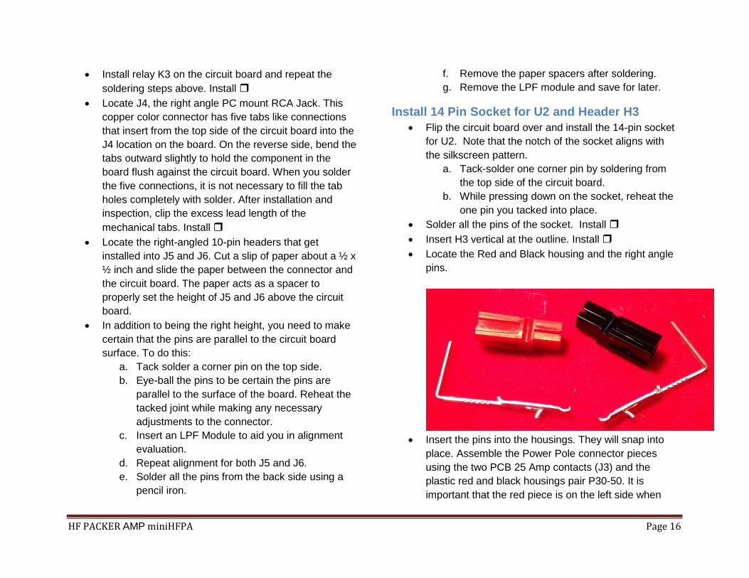
• Solder all the pins of the socket. Install • Insert H3 vertical at the outline. Install • Locate the Red and Black housing and the right angle
pins.
• Insert the pins into the housings. They will snap into
place. Assemble the Power Pole connector pieces using the two PCB 25 Amp contacts (J3) and the plastic red and black housings pair P30-50. It is important that the red piece is on the left side when
HF PACKER AMP miniHFPA Page 17
viewed from where you would plug in the power cable. The plastic pieces are tongue and groove to allow mating. Install
• Insert the J3 connector into the holes. The housing should lie flat on the top side of the circuit board with the leads parallel to the board and through the holes of J3. The red side inserts into pin 1 (+) of J3. Flip the board over and solder the pins. Cut the pins flush with the circuit board. You don’t want any protrusion of the cut leads. You can reheat the solder connection and press the stubble with the soldering iron so that the soldered pin recedes leaving a flat surface on the back side of the circuit board. Install
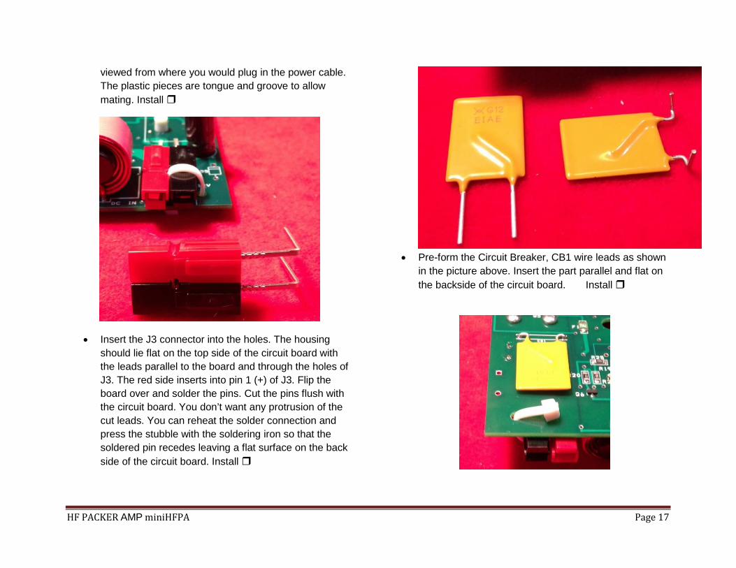
• Pre-form the Circuit Breaker, CB1 wire leads as shown
in the picture above. Insert the part parallel and flat on the backside of the circuit board. Install
HF PACKER AMP miniHFPA Page 18
• Use the Plastic Ty-wrap to secure the connector to the circuit board. Cut excess length after you cinch the wrap through the two holes provided on the circuit board. Install
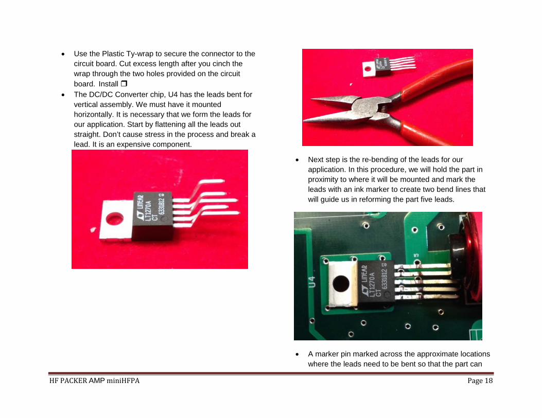
• The DC/DC Converter chip, U4 has the leads bent for vertical assembly. We must have it mounted horizontally. It is necessary that we form the leads for our application. Start by flattening all the leads out straight. Don’t cause stress in the process and break a lead. It is an expensive component.
• Next step is the re-bending of the leads for our application. In this procedure, we will hold the part in proximity to where it will be mounted and mark the leads with an ink marker to create two bend lines that will guide us in reforming the part five leads.
• A marker pin marked across the approximate locations where the leads need to be bent so that the part can
HF PACKER AMP miniHFPA Page 19
install on the circuit board. Two of the five leads are bent close to the body of the part. The three remaining alternating leads bend at the second scribe line.
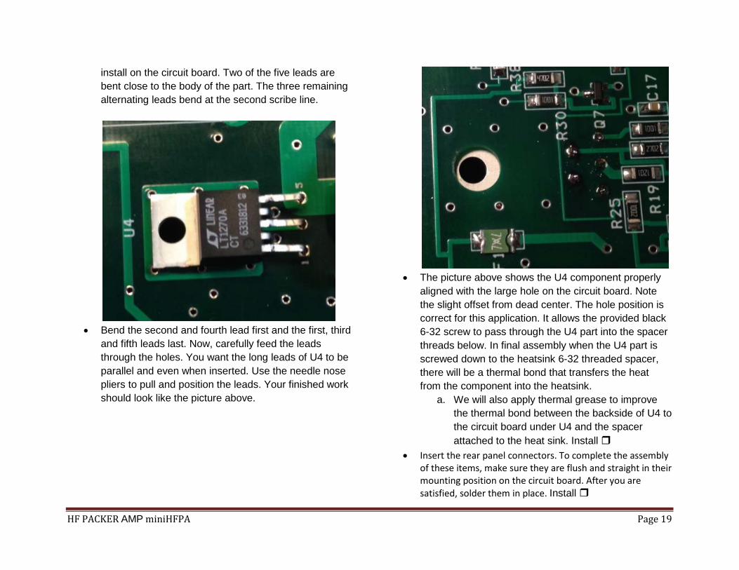
• Bend the second and fourth lead first and the first, third
and fifth leads last. Now, carefully feed the leads through the holes. You want the long leads of U4 to be parallel and even when inserted. Use the needle nose pliers to pull and position the leads. Your finished work should look like the picture above.
• The picture above shows the U4 component properly
aligned with the large hole on the circuit board. Note the slight offset from dead center. The hole position is correct for this application. It allows the provided black 6-32 screw to pass through the U4 part into the spacer threads below. In final assembly when the U4 part is screwed down to the heatsink 6-32 threaded spacer, there will be a thermal bond that transfers the heat from the component into the heatsink.
a. We will also apply thermal grease to improve the thermal bond between the backside of U4 to the circuit board under U4 and the spacer attached to the heat sink. Install
• Insert the rear panel connectors. To complete the assembly of these items, make sure they are flush and straight in their mounting position on the circuit board. After you are satisfied, solder them in place. Install
HF PACKER AMP miniHFPA Page 20
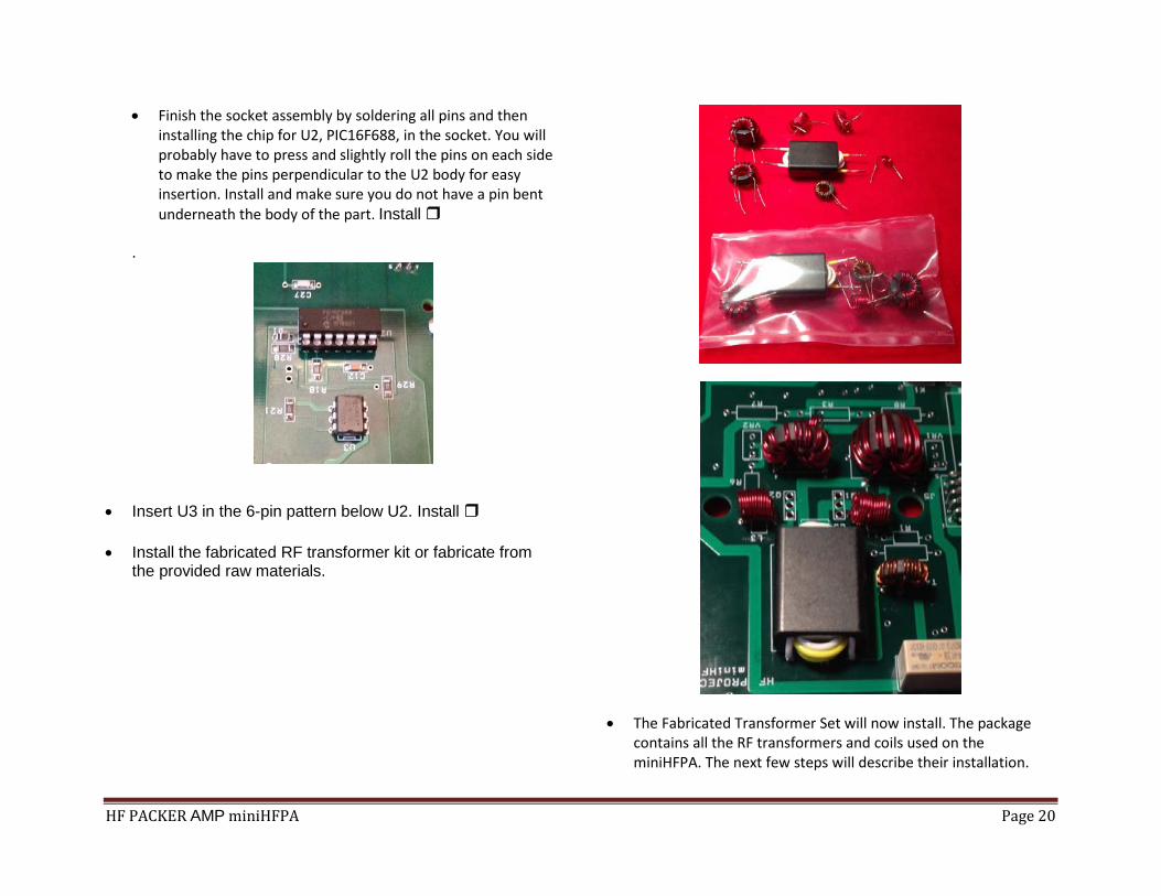
• Finish the socket assembly by soldering all pins and then installing the chip for U2, PIC16F688, in the socket. You will probably have to press and slightly roll the pins on each side to make the pins perpendicular to the U2 body for easy insertion. Install and make sure you do not have a pin bent underneath the body of the part. Install
.
• Insert U3 in the 6-pin pattern below U2. Install
• Install the fabricated RF transformer kit or fabricate from the provided raw materials.
• The Fabricated Transformer Set will now install. The package contains all the RF transformers and coils used on the miniHFPA. The next few steps will describe their installation.
HF PACKER AMP miniHFPA Page 21
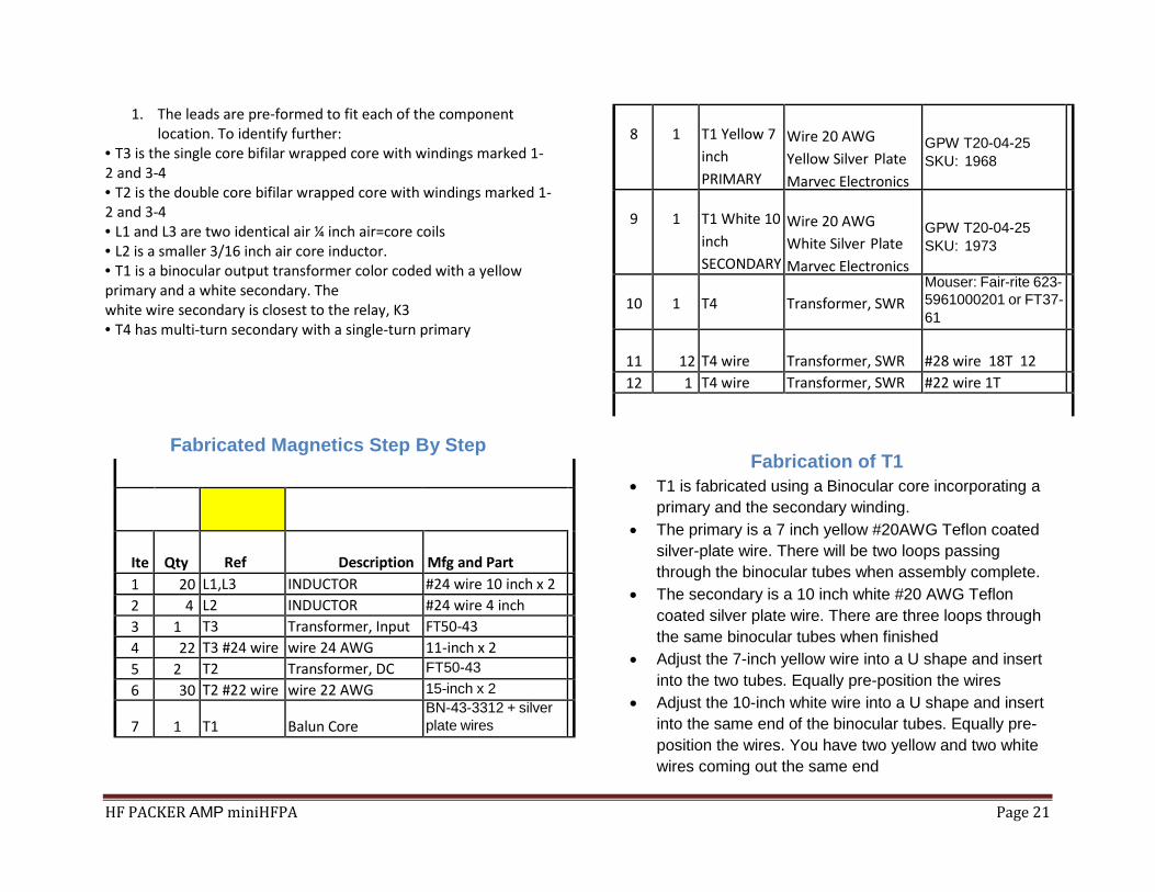
1. The leads are pre-formed to fit each of the component location. To identify further:
• T3 is the single core bifilar wrapped core with windings marked 1-2 and 3-4 • T2 is the double core bifilar wrapped core with windings marked 1-2 and 3-4 • L1 and L3 are two identical air ¼ inch air=core coils • L2 is a smaller 3/16 inch air core inductor. • T1 is a binocular output transformer color coded with a yellow primary and a white secondary. The white wire secondary is closest to the relay, K3 • T4 has multi-turn secondary with a single-turn primary
Fabricated Magnetics Step By Step
Ite
Qty
Ref
Description
Mfg and Part
1 20
L1,L3 INDUCTOR #24 wire 10 inch x 2 2 4
L2 INDUCTOR #24 wire 4 inch
3 1 T3 Transformer, Input FT50-43 4 22
T3 #24 wire wire 24 AWG 11-inch x 2
5 2 T2 Transformer, DC
FT50-43 6 30
T2 #22 wire wire 22 AWG 15-inch x 2
7
1
T1
Balun Core
BN-43-3312 + silver plate wires
8
1
T1 Yellow 7 inch PRIMARY
Wire 20 AWG Yellow Silver Plate Marvec Electronics
GPW T20-04-25 SKU: 1968
9
1
T1 White 10 inch SECONDARY
Wire 20 AWG White Silver Plate Marvec Electronics
GPW T20-04-25 SKU: 1973
10
1
T4
Transformer, SWR
Mouser: Fair-rite 623- 5961000201 or FT37- 61
11
12
T4 wire
Transformer, SWR
#28 wire 18T 12
12 1 T4 wire Transformer, SWR #22 wire 1T
Fabrication of T1 • T1 is fabricated using a Binocular core incorporating a
primary and the secondary winding. • The primary is a 7 inch yellow #20AWG Teflon coated
silver-plate wire. There will be two loops passing through the binocular tubes when assembly complete.
• The secondary is a 10 inch white #20 AWG Teflon coated silver plate wire. There are three loops through the same binocular tubes when finished
• Adjust the 7-inch yellow wire into a U shape and insert into the two tubes. Equally pre-position the wires
• Adjust the 10-inch white wire into a U shape and insert into the same end of the binocular tubes. Equally pre-position the wires. You have two yellow and two white wires coming out the same end
HF PACKER AMP miniHFPA Page 22
• Push one of the yellow wire leads through the adjacent tube. Push the other yellow wire lead through the other adjacent tube. Pull the leads tight. You completed the task with the yellow wire.
• Push the white wires through in the same manner. Pull the wires tight. Push the white wires through a final time through the adjacent tubes. You now have the yellow wire leads on one end, and the white wire leads on the other.
• You completed the winding of the core. • Trim about 3/8 inch length from each lead tip. Strip
each wire about 3/8 inch and lightly wet the tip. You are now ready to install the transformer on the board. The yellow primary (input) and white secondary (output).
• Insert the primary wires at holes 1 and 2. Pin 1 is the square pad.
• Insert the secondary into holes 3 and 4 • Pull leads snug and solder. Install
T1 with Yellow Leads Primary and White Leads Secondary
Fabrication and Assembly of T2
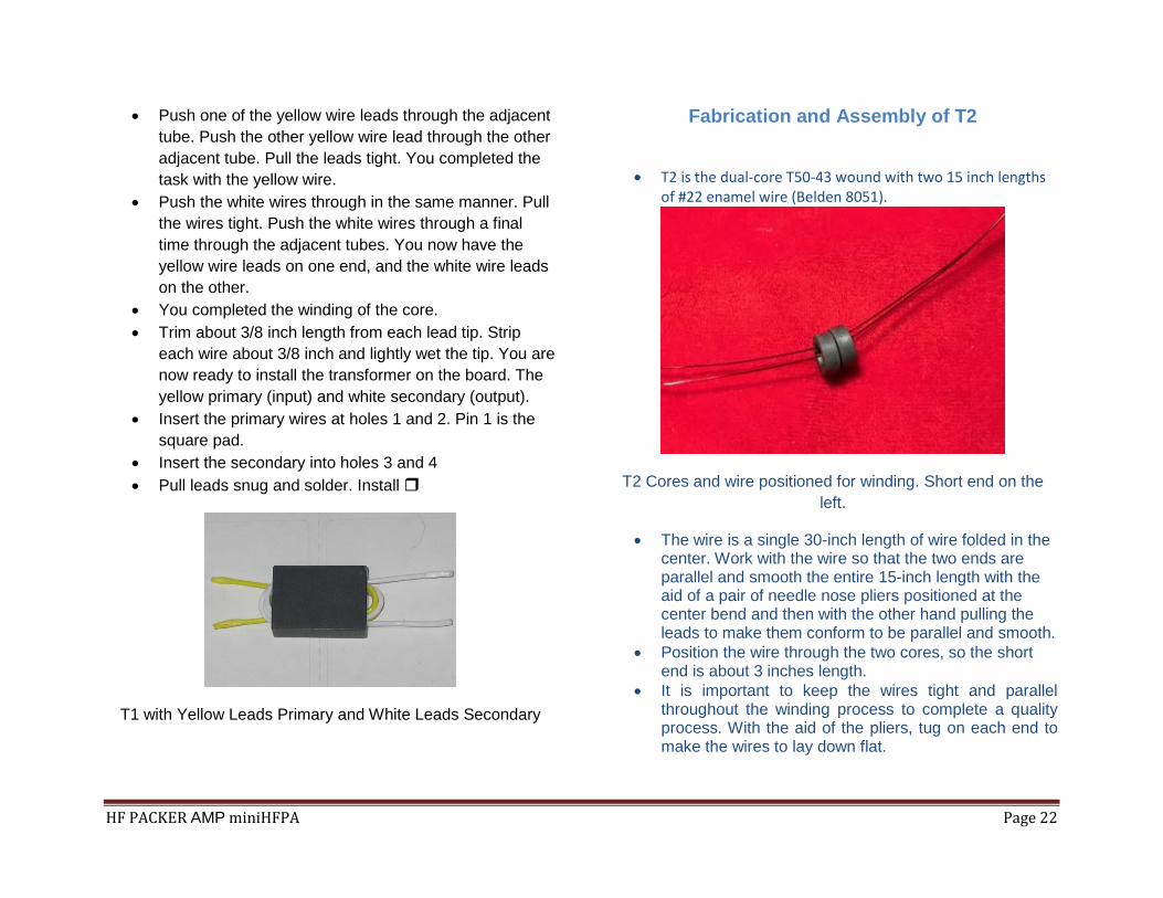
• T2 is the dual-core T50-43 wound with two 15 inch lengths of #22 enamel wire (Belden 8051).
T2 Cores and wire positioned for winding. Short end on the left.
• The wire is a single 30-inch length of wire folded in the center. Work with the wire so that the two ends are parallel and smooth the entire 15-inch length with the aid of a pair of needle nose pliers positioned at the center bend and then with the other hand pulling the leads to make them conform to be parallel and smooth.
• Position the wire through the two cores, so the short end is about 3 inches length.
• It is important to keep the wires tight and parallel throughout the winding process to complete a quality process. With the aid of the pliers, tug on each end to make the wires to lay down flat.
HF PACKER AMP miniHFPA Page 23
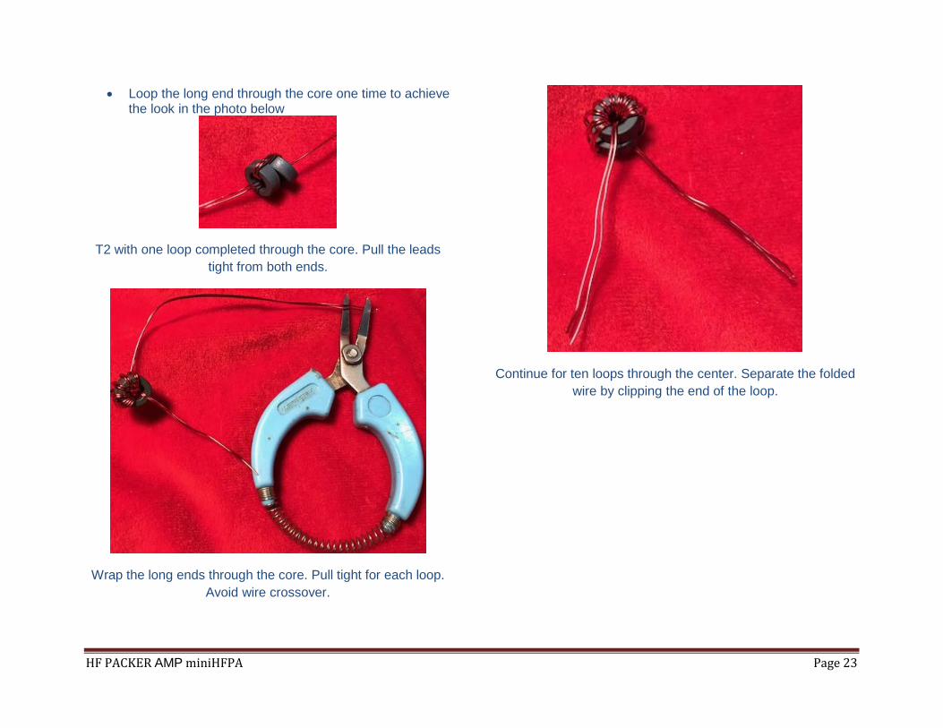
• Loop the long end through the core one time to achieve the look in the photo below
T2 with one loop completed through the core. Pull the leads tight from both ends.
Wrap the long ends through the core. Pull tight for each loop. Avoid wire crossover.
Continue for ten loops through the center. Separate the folded wire by clipping the end of the loop.
HF PACKER AMP miniHFPA Page 24
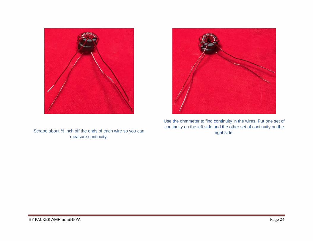
Scrape about ½ inch off the ends of each wire so you can measure continuity.
Use the ohmmeter to find continuity in the wires. Put one set of continuity on the left side and the other set of continuity on the
right side.
HF PACKER AMP miniHFPA Page 25
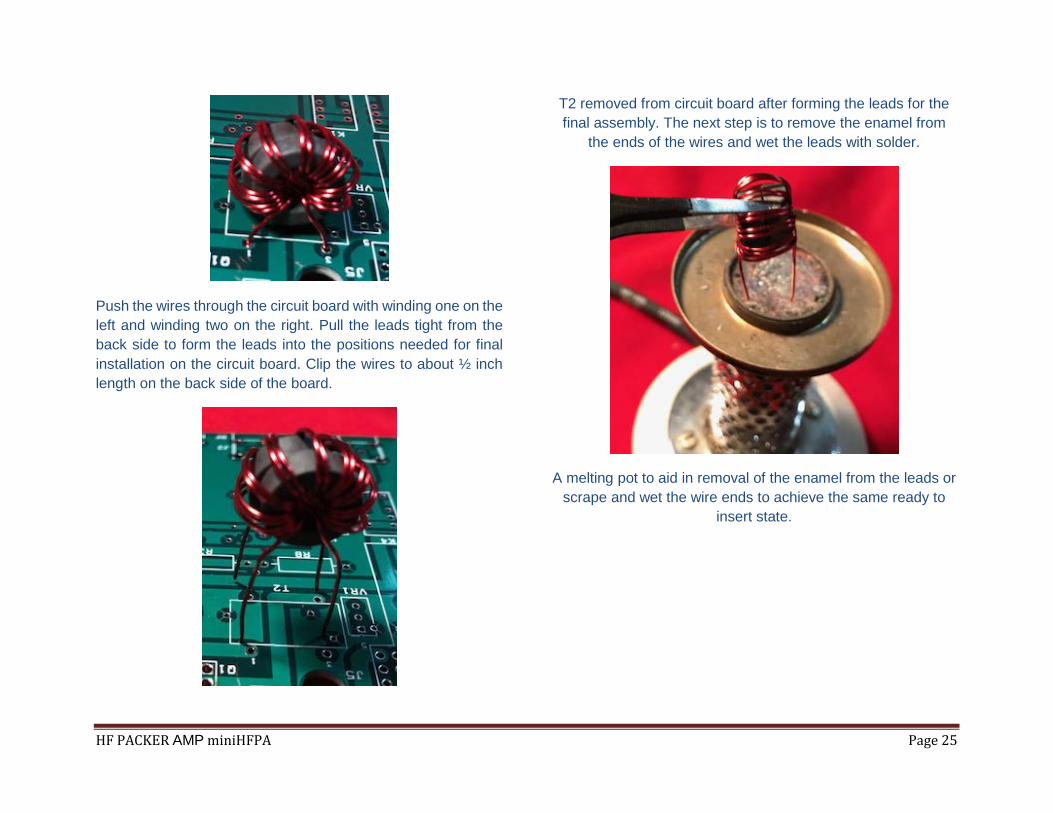
Push the wires through the circuit board with winding one on the left and winding two on the right. Pull the leads tight from the back side to form the leads into the positions needed for final installation on the circuit board. Clip the wires to about ½ inch length on the back side of the board.
T2 removed from circuit board after forming the leads for the final assembly. The next step is to remove the enamel from
the ends of the wires and wet the leads with solder.
A melting pot to aid in removal of the enamel from the leads or scrape and wet the wire ends to achieve the same ready to
insert state.
HF PACKER AMP miniHFPA Page 26
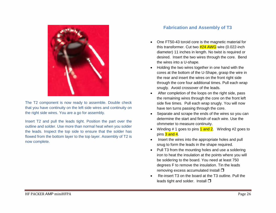
The T2 component is now ready to assemble. Double check that you have continuity on the left side wires and continuity on the right side wires. You are a go for assembly.
Insert T2 and pull the leads tight. Position the part over the outline and solder. Use more than normal heat when you solder the leads. Inspect the top side to ensure that the solder has flowed from the bottom layer to the top layer. Assembly of T2 is now complete.
Fabrication and Assembly of T3
• One FT50-43 toroid core is the magnetic material for this transformer. Cut two #24 AWG wire (0.022-inch diameter) 11 inches in length. No twist is required or desired. Insert the two wires through the core. Bend the wires into a U-shape.
• Holding the two wires together in one hand with the cores at the bottom of the U-Shape, grasp the wire in the rear and insert the wires on the front right side through the core four additional times. Pull each wrap snugly. Avoid crossover of the leads.
• After completion of the loops on the right side, pass the remaining wires through the core on the front left side five times. Pull each wrap snugly. You will now have ten turns passing through the core.
• Separate and scrape the ends of the wires so you can determine the start and finish of each wire. Use the ohmmeter to measure continuity.
• Winding # 1 goes to pins 1 and 2. Winding #2 goes to pins 3 and 4.
• Insert the wires into the appropriate holes and pull snug to form the leads in the shape required.
• Pull T3 from the mounting holes and use a soldering iron to heat the insulation at the points where you will be soldering to the board. You need at least 750 degrees F to remove the insulation. Tin the leads removing excess accumulated Install
• Re-insert T3 on the board at the T3 outline. Pull the leads tight and solder. Install
HF PACKER AMP miniHFPA Page 27
• Trim the excess lead length and reflow connections.
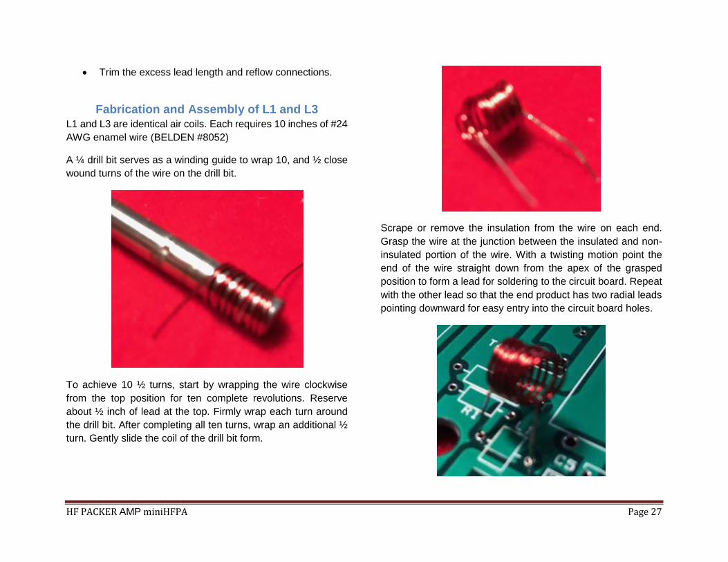
Fabrication and Assembly of L1 and L3 L1 and L3 are identical air coils. Each requires 10 inches of #24 AWG enamel wire (BELDEN #8052)
A ¼ drill bit serves as a winding guide to wrap 10, and ½ close wound turns of the wire on the drill bit.
To achieve 10 ½ turns, start by wrapping the wire clockwise from the top position for ten complete revolutions. Reserve about ½ inch of lead at the top. Firmly wrap each turn around the drill bit. After completing all ten turns, wrap an additional ½ turn. Gently slide the coil of the drill bit form.
Scrape or remove the insulation from the wire on each end. Grasp the wire at the junction between the insulated and non-insulated portion of the wire. With a twisting motion point the end of the wire straight down from the apex of the grasped position to form a lead for soldering to the circuit board. Repeat with the other lead so that the end product has two radial leads pointing downward for easy entry into the circuit board holes.
HF PACKER AMP miniHFPA Page 28
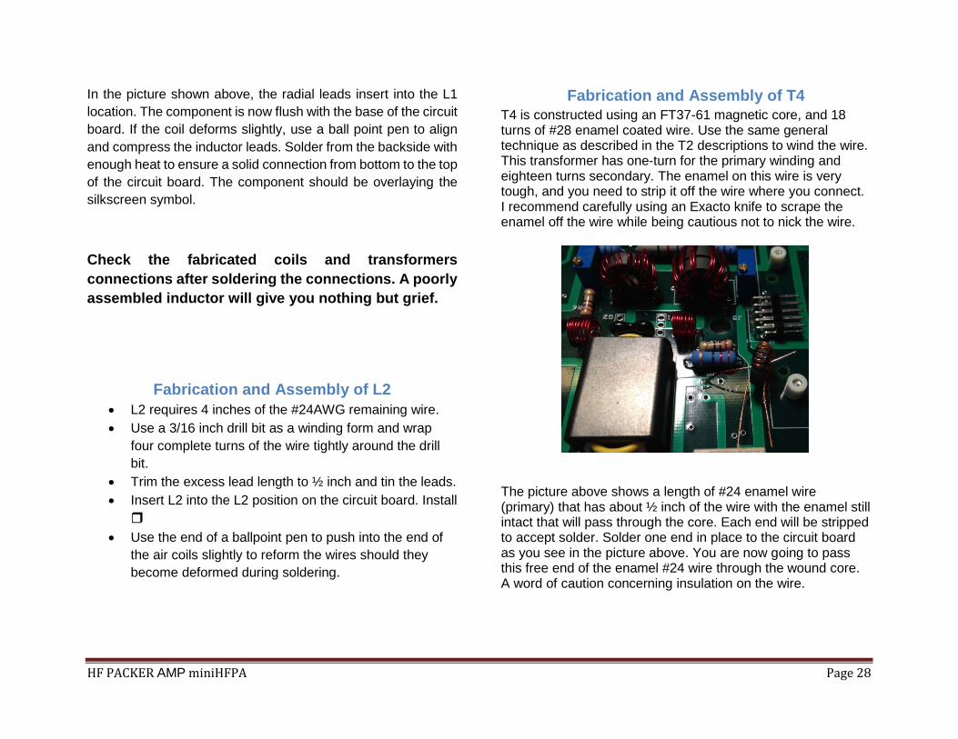
In the picture shown above, the radial leads insert into the L1 location. The component is now flush with the base of the circuit board. If the coil deforms slightly, use a ball point pen to align and compress the inductor leads. Solder from the backside with enough heat to ensure a solid connection from bottom to the top of the circuit board. The component should be overlaying the silkscreen symbol.
Check the fabricated coils and transformers connections after soldering the connections. A poorly assembled inductor will give you nothing but grief.
Fabrication and Assembly of L2 • L2 requires 4 inches of the #24AWG remaining wire. • Use a 3/16 inch drill bit as a winding form and wrap
four complete turns of the wire tightly around the drill bit.
• Trim the excess lead length to ½ inch and tin the leads. • Insert L2 into the L2 position on the circuit board. Install
• Use the end of a ballpoint pen to push into the end of the air coils slightly to reform the wires should they become deformed during soldering.
Fabrication and Assembly of T4 T4 is constructed using an FT37-61 magnetic core, and 18 turns of #28 enamel coated wire. Use the same general technique as described in the T2 descriptions to wind the wire. This transformer has one-turn for the primary winding and eighteen turns secondary. The enamel on this wire is very tough, and you need to strip it off the wire where you connect. I recommend carefully using an Exacto knife to scrape the enamel off the wire while being cautious not to nick the wire.
The picture above shows a length of #24 enamel wire (primary) that has about ½ inch of the wire with the enamel still intact that will pass through the core. Each end will be stripped to accept solder. Solder one end in place to the circuit board as you see in the picture above. You are now going to pass this free end of the enamel #24 wire through the wound core. A word of caution concerning insulation on the wire.
HF PACKER AMP miniHFPA Page 29
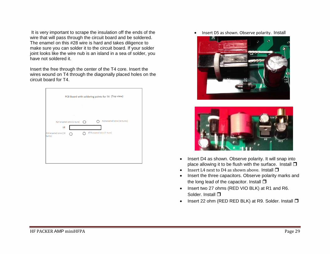
It is very important to scrape the insulation off the ends of the wire that will pass through the circuit board and be soldered. The enamel on this #28 wire is hard and takes diligence to make sure you can solder it to the circuit board. If your solder joint looks like the wire nub is an island in a sea of solder, you have not soldered it. Insert the free through the center of the T4 core. Insert the wires wound on T4 through the diagonally placed holes on the circuit board for T4.
• Insert D5 as shown. Observe polarity. Install
• Insert D4 as shown. Observe polarity. It will snap into place allowing it to be flush with the surface. Install
• Insert L4 next to D4 as shown above. Install • Insert the three capacitors. Observe polarity marks and
the long lead of the capacitor. Install • Insert two 27 ohms (RED VIO BLK) at R1 and R6.
Solder. Install • Insert 22 ohm (RED RED BLK) at R9. Solder. Install

HF PACKER AMP miniHFPA Page 30
• Insert VR1 and VR2 (Blue Trim Potentiometers) as shown in the picture above. Note the position of the adjustment screw. The square pad is the indicator of the screw position when inserting the part. Ensure these components are flush with the circuit board by bending the top and bottom leads out slightly to hold the part in position. Solder. Turn the pots at least ten turns counter-clockwise. Note: the component does not have a clicking sound when the screw reaches the end of their travel. No damage will happen if you keep turning the screws. Install
• Insert C5; a dip silver mica capacitor marked 47 (47pf) into the two mounting holes for C5. This component is directly behind T1, shown in the lower left corner of the drawing above. Mount the component with the body flush with the top of the circuit board, C5 symbol. Solder from the backside and clip the excess lead length. Install
PI-Resistive Network Installation • Choose to build your miniHFPA for the desired maximum RF
Input that your transceiver supplies. The miniHFPA output power is the same in any case. Overdriving the amp will cause excessive current. Although the miniHFPA has max current sensing and shutdown, you are putting your amp in harm’s way and therefore susceptible to a possible failure. Protection devices are much slower to operate than the electrons flowing through your circuits. It depends upon the amount of over-current, and the internal temperature builds up exceeding the capacity for the MOSFET case to drain that heat away from the device.
1. This option is available so you can match the amplifier input requirements to the transceiver output characteristic. You may find it advantages to use a lower power on the transceiver, if you have a choice, to improve on battery life. 5.0 W Max RF Input (standard)
R3 62 ohm, 2W (BLU-RED-BLK) R7/R8 100 ohm, 2W (BRN-BLK-BRN)
2.5W Max RF Input (option) R3 39 ohm, 2W (ORN-YEL-BLK)
R7/R8 160 ohm, 2W (BRN-BLU-BRN) 1.0W Max RF Input (option)
R3 12 ohm, 1W (BRN-RED-BLK) R7/R8 430 ohm, 2W (YEL-ORN-BRN)
Note: As a word of caution, some rigs may allow you to set 1W as the output level but revert to 5W while tuning.
• Install the version that you want to use. I suggest using an ohmmeter to confirm the resistor values. Install

HF PACKER AMP miniHFPA Page 31
PI-Resistive Network and Bias Pots • In the picture below, the standard 5.0W max RF Input
resistor values are visible in the foreground.
• Note the location of the adjustment screw in the picture
above. The square pin on the circuit board is your indicator of the pot adjustment position. Turn the pots about ten turns counter clockwise. You will not hear a click at the end of the travel range.
Bottom Cover Assembly The bottom cover has the holes for the connectors on end.
• Install four Rubber Bumpers. You will need small hand tool pliers and a tiny screwdriver for this assembly. Locate the four black rubber bumpers. On the outside of the bottom cover, insert the rubber bumpers one at a time through the four corner holes. You will find it difficult to do unless you use a technique to get the rubber through the hole. A tiny blade screwdriver can be used to push the rubber into and through the hole
while you are pressing down with your thumb on the bumper head. 1. Place the bumper on the hole and press firmly
down with the thumb. 2. With a tiny screwdriver or equivalent, push in on the
side of the rubber that is not going into the hole. You may have to work around the perimeter pressing the rubber into the hole while maintaining pressure on the bumper head.
3. Once you start seeing some rubber passing through the hole. After you get about 1/8th inch passing through the hole, you can use small hand tool pliers to grasp the rubber and pull the rubber further through the hole. You will have to tug in all lateral directions to make the rubber enter the hole.
4. Pull and work the rubber until the rubber bumper body is flush with the bottom of the bottom cover.
5. Install
Set the bottom cover aside for future use during final assembly.
HF PACKER AMP miniHFPA Page 32
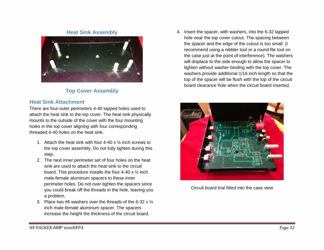
Heat Sink Assembly
Top Cover Assembly
Heat Sink Attachment There are four outer perimeters 4-40 tapped holes used to attach the heat sink to the top cover. The heat sink physically mounts to the outside of the cover with the four mounting holes in the top cover aligning with four corresponding threaded 4-40 holes on the heat sink.
1. Attach the heat sink with four 4-40 x ¼ inch screws to the top cover assembly. Do not fully tighten during this step.
2. The next inner perimeter set of four holes on the heat sink are used to attach the heat sink to the circuit board. This procedure installs the four 4-40 x ½ inch male-female aluminum spacers to these inner perimeter holes. Do not over tighten the spacers since you could break off the threads in the hole, leaving you a problem.
3. Place two #6 washers over the threads of the 6-32 x ½ inch male-female aluminum spacer. The spacers increase the height the thickness of the circuit board.
4. Insert the spacer, with washers, into the 6-32 tapped hole near the top cover cutout. The spacing between the spacer and the edge of the cutout is too small. (I recommend using a nibbler tool or a round file tool on the case just at the point of interference). The washers will displace to the side enough to allow the spacer to tighten without washer binding with the top cover. The washers provide additional 1/16 inch length so that the top of the spacer will be flush with the top of the circuit board clearance hole when the circuit board inserted.
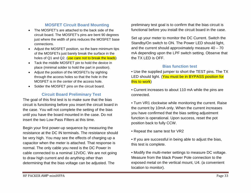
Circuit board trial fitted into the case view
HF PACKER AMP miniHFPA Page 33
MOSFET Circuit Board Mounting • The MOSFET’s are attached to the back side of the
circuit board. The MOSFET’s pins are bent 90 degrees just where the width of pins reduces the MOSFET base connections.
• Adjust the MOSFET position, so the bare minimum tips of the MOSFETs just barely break the surface in the holes of Q1 and Q2. (use care not to break the leads)
• Tack the middle MOSFET pin to hold the device in place (minimal solder to hold the part in position).
• Adjust the position of the MOSFETs by sighting through the access holes so that the hole in the MOSFET is in the center of the access hole.
• Solder the MOSFET pins on the circuit board.
Circuit Board Preliminary Test The goal of this first test is to make sure that the bias circuit is functioning before you insert the circuit board in the case. You will not complete the setting of the bias until you have the board mounted in the case. Do not insert the two Low Pass Filters at this time.
Begin your first power-up sequence by measuring the resistance at the DC IN terminals. The resistance should be very high. You may see the effects of charging up a capacitor when the meter is attached. That response is normal. The only cable you need is the DC Power In cable connected to a nominal 12VDC. We are not going to draw high current and do anything other than determining that the bias voltage can be adjusted. The
preliminary test goal is to confirm that the bias circuit is functional before you install the circuit board in the case.
Set up your meter to monitor the DC Current. Switch the Standby/On switch to ON. The Power LED should light, and the current should approximately measure 40 – 70 mA depending upon the LPF switch setting. Observe that the TX LED is OFF.
Bias function test • Use the supplied jumper to short the TEST pins. The TX LED should light. (You must be in BYPASS position for this to work)
• Current increases to about 110 mA while the pins are connected.
• Turn VR1 clockwise while monitoring the current. Raise the current by 10mA only. When the current increases you have confirmed that the bias setting adjustment function is operational. Upon success, reset the pot position back to fully CCW.
• Repeat the same test for VR2
• If you are successful in being able to adjust the bias, this test is complete.
• Modify the multi-meter settings to measure DC voltage. Measure from the black Power Pole connection to the exposed metal on the vertical mount, U4. (a convenient location to monitor).
HF PACKER AMP miniHFPA Page 34
• Switch the “On/Standby” Power switch back to ON and jumper the TEST pins. The measured voltage should be approximately 29VDC while the TX LED is ON. If you do not light the TX LED when you attach the jumper, turn the power off and try again. (Rapid or multiple transitions on the TEST jumper will cause the TX LED not to light).
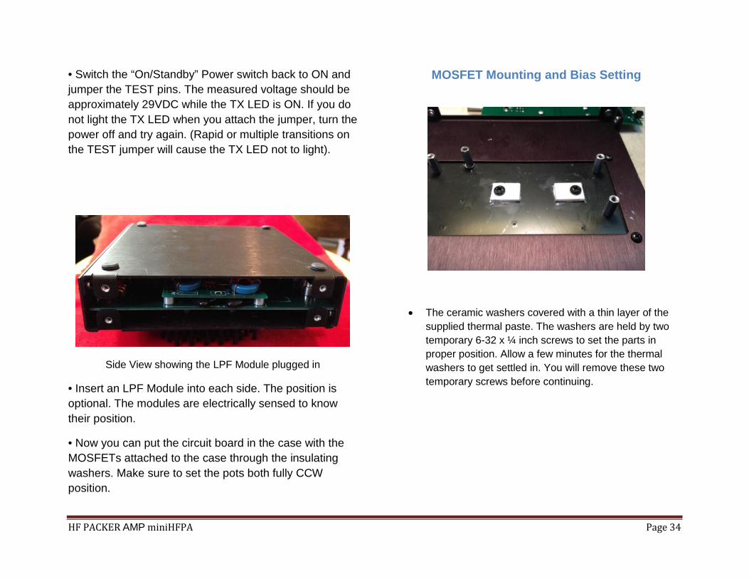
Side View showing the LPF Module plugged in
• Insert an LPF Module into each side. The position is optional. The modules are electrically sensed to know their position.
• Now you can put the circuit board in the case with the MOSFETs attached to the case through the insulating washers. Make sure to set the pots both fully CCW position.
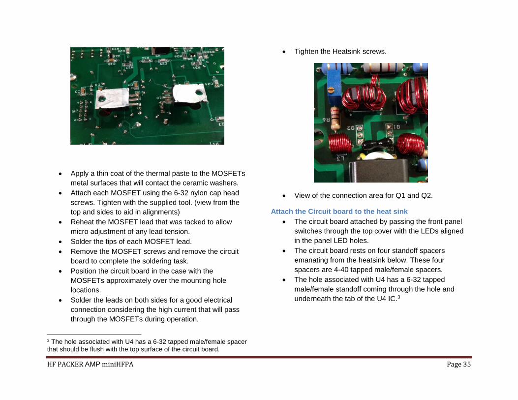
MOSFET Mounting and Bias Setting
• The ceramic washers covered with a thin layer of the supplied thermal paste. The washers are held by two temporary 6-32 x ¼ inch screws to set the parts in proper position. Allow a few minutes for the thermal washers to get settled in. You will remove these two temporary screws before continuing.
HF PACKER AMP miniHFPA Page 35
• Apply a thin coat of the thermal paste to the MOSFETs metal surfaces that will contact the ceramic washers.
• Attach each MOSFET using the 6-32 nylon cap head screws. Tighten with the supplied tool. (view from the top and sides to aid in alignments)
• Reheat the MOSFET lead that was tacked to allow micro adjustment of any lead tension.
• Solder the tips of each MOSFET lead. • Remove the MOSFET screws and remove the circuit
board to complete the soldering task. • Position the circuit board in the case with the
MOSFETs approximately over the mounting hole locations.
• Solder the leads on both sides for a good electrical connection considering the high current that will pass through the MOSFETs during operation.
3 The hole associated with U4 has a 6-32 tapped male/female spacer that should be flush with the top surface of the circuit board.
• Tighten the Heatsink screws.
• View of the connection area for Q1 and Q2.
Attach the Circuit board to the heat sink • The circuit board attached by passing the front panel
switches through the top cover with the LEDs aligned in the panel LED holes.
• The circuit board rests on four standoff spacers emanating from the heatsink below. These four spacers are 4-40 tapped male/female spacers.
• The hole associated with U4 has a 6-32 tapped male/female standoff coming through the hole and underneath the tab of the U4 IC.3
HF PACKER AMP miniHFPA Page 36
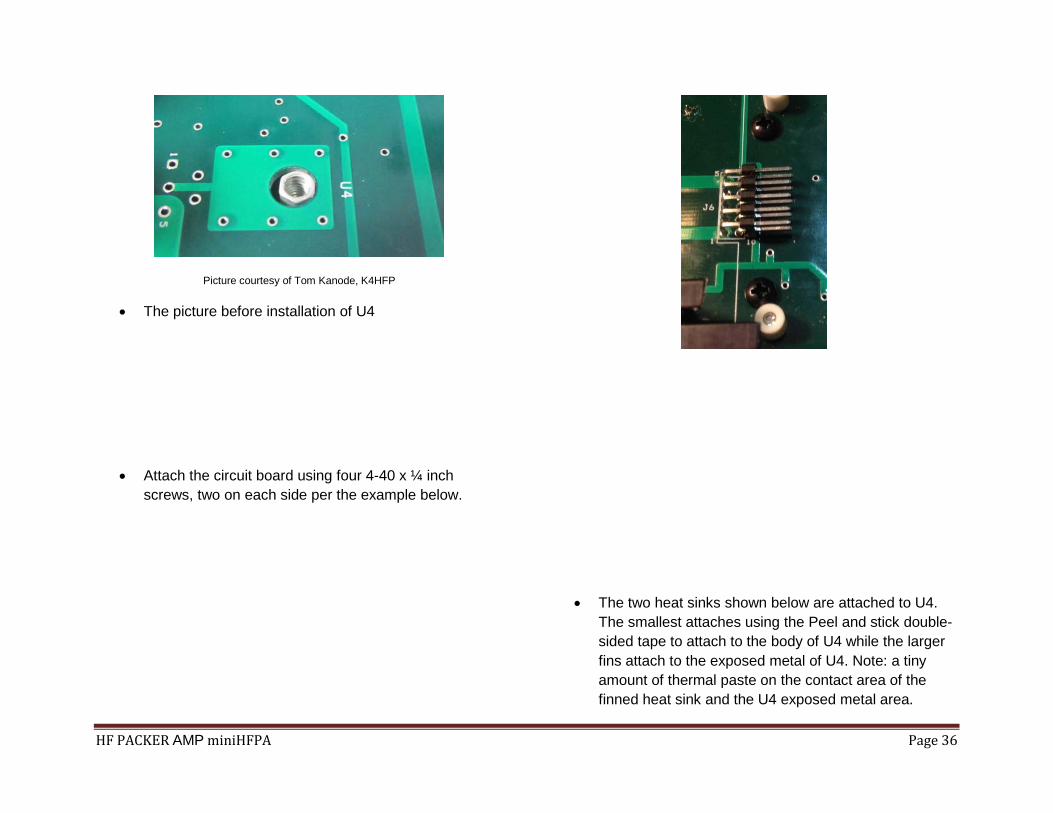
Picture courtesy of Tom Kanode, K4HFP
• The picture before installation of U4
• Attach the circuit board using four 4-40 x ¼ inch screws, two on each side per the example below.
• The two heat sinks shown below are attached to U4. The smallest attaches using the Peel and stick double-sided tape to attach to the body of U4 while the larger fins attach to the exposed metal of U4. Note: a tiny amount of thermal paste on the contact area of the finned heat sink and the U4 exposed metal area.
HF PACKER AMP miniHFPA Page 37
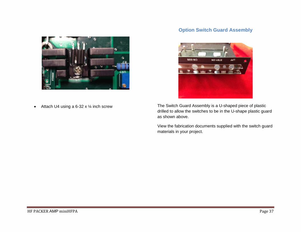
• Attach U4 using a 6-32 x ¼ inch screw
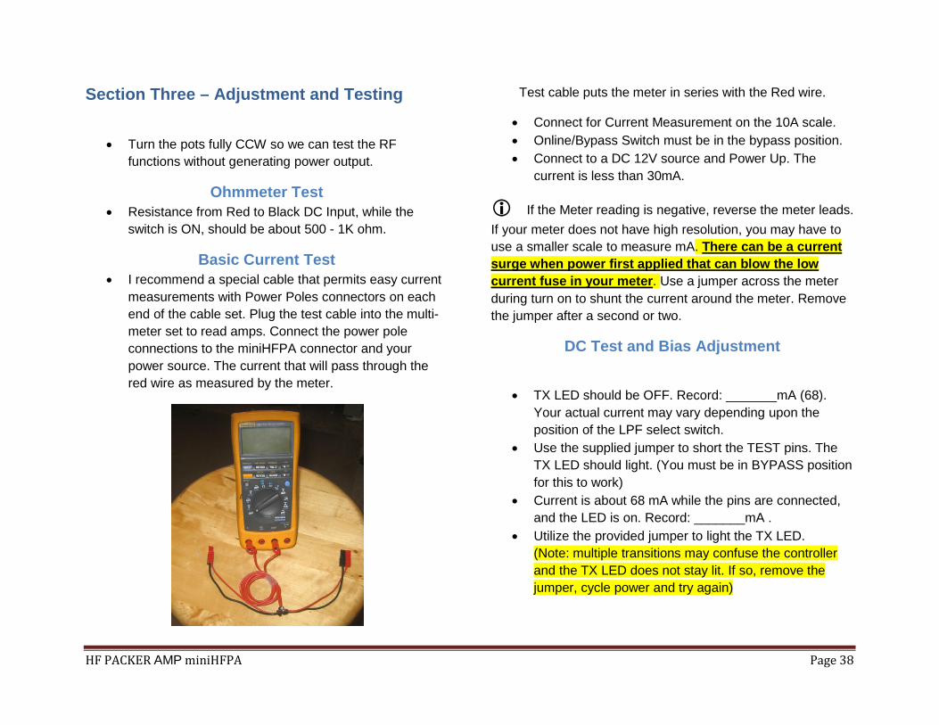
Option Switch Guard Assembly
The Switch Guard Assembly is a U-shaped piece of plastic drilled to allow the switches to be in the U-shape plastic guard as shown above.
View the fabrication documents supplied with the switch guard materials in your project.
HF PACKER AMP miniHFPA Page 38
Section Three – Adjustment and Testing
• Turn the pots fully CCW so we can test the RF functions without generating power output.
Ohmmeter Test • Resistance from Red to Black DC Input, while the
switch is ON, should be about 500 - 1K ohm.
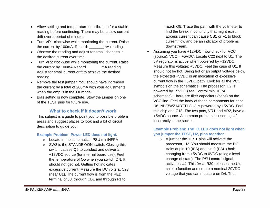
Basic Current Test • I recommend a special cable that permits easy current
measurements with Power Poles connectors on each end of the cable set. Plug the test cable into the multi-meter set to read amps. Connect the power pole connections to the miniHFPA connector and your power source. The current that will pass through the red wire as measured by the meter.
Test cable puts the meter in series with the Red wire.
• Connect for Current Measurement on the 10A scale. • Online/Bypass Switch must be in the bypass position. • Connect to a DC 12V source and Power Up. The
current is less than 30mA.
If the Meter reading is negative, reverse the meter leads. If your meter does not have high resolution, you may have to use a smaller scale to measure mA. There can be a current surge when power first applied that can blow the low current fuse in your meter. Use a jumper across the meter during turn on to shunt the current around the meter. Remove the jumper after a second or two.
DC Test and Bias Adjustment
• TX LED should be OFF. Record: _______mA (68). Your actual current may vary depending upon the position of the LPF select switch.
• Use the supplied jumper to short the TEST pins. The TX LED should light. (You must be in BYPASS position for this to work)
• Current is about 68 mA while the pins are connected, and the LED is on. Record: _______mA .
• Utilize the provided jumper to light the TX LED. (Note: multiple transitions may confuse the controller and the TX LED does not stay lit. If so, remove the jumper, cycle power and try again)
HF PACKER AMP miniHFPA Page 39
• Allow settling and temperature equilibration for a stable reading before continuing. There may be a slow current drift over a period of minutes.
• Turn VR1 clockwise while monitoring the current. Raise the current by 100mA. Record: _______mA reading.
• Observe the reading and adjust for small changes in the desired current over time.
• Turn VR2 clockwise while monitoring the current. Raise the current by 100mA Record _______mA reading. Adjust for small current drift to achieve the desired reading.
• Remove the test jumper. You should have increased the current by a total of 200mA with your adjustments when the amp is in the TX mode.
• Bias setting is now complete. Stow the jumper on one of the TEST pins for future use.
What to check if it doesn’t work This subject is a guide to point you to possible problem areas and suggest places to look and a bit of circuit description to guide you.
Example Problem: Power LED does not light. o Locate in the schematics: PSU miniHFPA o SW3 is the STANDBY/ON switch. Closing this
switch causes Q5 to conduct and deliver a +12VDC source (for internal board use). Feel the temperature of Q5 when you switch ON. It should not get hot. Getting hot indicates excessive current. Measure the DC volts at C23 (near U1). The current flow is from the RED terminal of J3, through CB1 and through F1 to
reach Q5. Trace the path with the voltmeter to find the break in continuity that might exist. Excess current can cause CB1 or F1 to block current flow and be an indicator of problems downstream.
• Assuming you have +12VDC, now check for VCC (source). VCC = +5VDC. Locate C22 next to U1. The 5V regulator is active when powered by +12VDC. Measure this voltage: +5VDC. Feel the case of U1. It should not be hot. Being hot or an output voltage below the expected +5VDC is an indication of excessive current flow in the +5VDC path. Look for all the VCC symbols on the schematics. The processor, U2 is powered by +5VDC (see Control miniHFPA schematic). There are filter capacitors (caps) on the VCC line. Feel the body of these components for heat. U6, NL27WZ14DTT1G IC is powered by +5VDC. Feel this chip and C18. The two pots, VR1 and VR2, have a +5VDC source. A common problem is inserting U2 incorrectly in the socket.
Example Problem: The TX LED does not light when you jumper the TEST, H2, pins together.
o A jumper the TEST pins will activate the processor, U2. You should measure the DC Volts at pin 10 (IPS) and pin 9 (PSU) both changing from +5VDC to 0VDC (a logic level change of state). The PSU control signal activates U4. This 0V at R30 releases the U4 chip to function and create a nominal 29VDC voltage that you can measure on D4. The
HF PACKER AMP miniHFPA Page 40
voltage measures a nominal +12V when U4 is OFF and +29VDC when ON.
o THE IPS signal when measuring 0V should activate the intelligent power switch, U5. The evidence of this activation is the lighting of the TX LED, LED3. The output voltage from U5 is labeled SWV (switched voltage).
Example Problem: The current does not increase when you turn VR1 or VR2 clockwise.
• Note: it will take several turns of the potentiometer (pot) before you see an increase in current. Common reasons are:
o The DC Volts does not increase at the gates of Q1 and Q2. The problem may be due to a continuity problem through L1 or L3. You can measure this voltage at C6 and C10.
o The DC Current does not increase even though you can measure the bias voltage at C6 and C10: The problem is usually because of improper installation of T2
o The Transformer, T2 has the windings, not in the correct configuration. It is possible to insert the wires of T2 in such a manner that the SWV voltage (29VDC) do not reach the drains of Q1 and Q2. It is practically impossible to determine by ohmmeter measurement with T2 soldered into the circuit board. You can, however, measure the +29VDC on the drains of Q1 and Q2 (MOSFET AMP miniHFPA schematic).
• The above steps complete the bench test before you formally install the circuit board in the case.
Tests with Circuit Board Installed • You have resolved any circuit board problems you
detected. Complete the assembly by installing the circuit board in the case having the MOSFETs attached to the heat sink and the U4 IC attached to the heat sink.
Install two LPF Modules • Insert the 60/40 Module on one side and the 30/20
Module on the other side. It does not matter which side you install the modules.
• The selected LPF module will light the LED for that LPF.
Test Mode Setup
• Online/Bypass Switch placed in Bypass position • Attach a Wattmeter and a dummy load combination to
the BNC RF Output connector. • Connect the transceiver to the BNC RF Input
Connector. • Set the INLINE/BYPASS switch to BYPASS. • Set the transceiver Power Setting for a Low Power
setting (about 1W) if available. • Key XCVR. The 1W of power should display on
Wattmeter and SWR should 1.0:1 Record _____ W
HF PACKER AMP miniHFPA Page 41
RF Signal Testing
• Switch the Online/Bypass Switch to Online. Key the XCVR. The LED lights. (1W RF drive)
• Release XCVR KEY. The LED is off. • Measure from case ground to the metal case of diode
D4. Key the XCVR. The voltage switches from 0.0VDC to about 29.5VDC.(plus or minus 0.5VDC typical)
• The CW/SSB toggle switch controls the hang time of the amp when using RF keying. Note the time difference that the TX LED is ON in CW vs. SSB. Momentarily key the transceiver to observe the hang time in CW and SSB position of the switch.
• Short the inner pin to the outer pin of the PTT jack while observing the TX light on the panel.
• The LED lights. Remove the shorted PTT input. The TX LED is off. Note: Using PTT overrides the internal hang time delay for CW or SSB modes.
Voltage Test • It is handy to have a voltmeter available for voltage
measurements while monitoring current. If a second meter not available, reconfigure meter to measure voltage.
• Re-connect DC power if not connected at this time. • Measure from Case to the rectifier tab, D4, next to the
electrolytic capacitors. The voltage is the DC Input Voltage. Approximately 13.6V. Record _____ VDC
• Use the screwdriver again to jumper the TEST pins of H3. The LED lights and you measure about 29.2VDC. Record _____VDC
At this point, you have proven the functionality of the miniHFPA, and you have completed the adjustments.
LT1270ACT Alert Notice "Be careful when probing around the DC‐DC Converter chip. I
have received one user report of the chip failure and going violently up in flames when grounding pin two, the flyback sensor to control the output voltage. The voltage divider R13 and R16 are used to tell the sensor the output voltage. The LT1270A will try to increase the voltage on pin four until the voltage on pin two from the voltage divider reaches 1.24V. A fault condition can result in dangerously high voltages on pin 4 when pin two is mistakenly grounded. Also note, that the middle pin 3 is the ground while pin four is an output voltage of about 30V.
Those two pins could easily short-circuit while probing. A safer solution is to measure the input voltage (pin 5) at the cathode of D5. Measure the output voltage (pin 4) at the anode of D4. Measure the fly-back voltage (pin 2) at R13. Pin 1 is the control pin that is controlled by Q7 when driven into conduction by the signal, PSU. Be very careful!"
RF Power Testing
HF PACKER AMP miniHFPA Page 42
• Attach a fused 12VDC power source capable of supplying 10A continuous current.
• Monitor Current • Your amp is 1W, 2.5W or 5W max RF input. You do
not want to exceed the max RF input because of the over-current situation that will result.
• In this manual, we are using the 5W setting • Select an LPF band that matches the transceiver band. • In BYPASS mode, adjust the power out to 5W ______ • Switch to the ONLINE position and key down for a few
seconds, Observe the power output and current. • Record your power output and current for each band in
the Frequency vs. Watts vs. Amps Table. • Plot your Power Out and Amps results vs. Frequency.
If you see an unusual spike up in current or drop in power, your LPF may be suspect. A fault may cause the SWR LED to light and switched the amp to bypass.
This chart was recorded on an earlier model but also applies to the miniHFPA.
FREQ MHZ WATTS AMPS 1.9 45 7.5 3.9 40 7 7.3 35 7 10 35 8.3 14.3 35 7.3 18.7 29 8.2 21.3 30 6.7 24.9 25 5.5
28.4 20 4.5 Frequency vs. Watts vs. Amps Table
Frequency vs. Watts vs. Amps Plot
Power Input Constant at 5W set for each band
PTT Connections FLEX 1500 and FT817 FLEX 1500 – Connect the center wire from the PTT jack to pin 3 of a serial connector which corresponds to the Flex 1500 Flexwire connector on the back of the radio. This connection allowed the Flex 1500 to key the Packer Amp. Do not connect the ground connection as the Amp and Radio are the same ground. Using an additional ground connection has been reported to cause distortion.
FT817 – Connect the center wire from the PTT jack to pin 1 of the ACC jack on the FT817 (PTT). Do not connect the ground since the Amp and Radio use the same ground. Using an
0
10
20
30
40
50
0 10 20 30
WATTS
AMPS
WATTS
AMPS
HF PACKER AMP miniHFPA Page 43
additional ground connection has been reported to cause distortion.
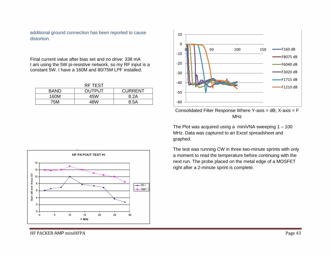
Final current value after bias set and no drive: 338 mA I am using the 5W pi-resistive network, so my RF input is a constant 5W. I have a 160M and 80/75M LPF installed.
RF TEST BAND OUTPUT CURRENT 160M 45W 8.2A 75M 48W 8.5A
Consolidated Filter Response Where Y-axis = dB; X-axis = F
MHz
The Plot was acquired using a miniVNA sweeping 1 – 100 MHz. Data was captured to an Excel spreadsheet and graphed.
The test was running CW in three two-minute sprints with only a moment to read the temperature before continuing with the next run. The probe placed on the metal edge of a MOSFET right after a 2-minute sprint is complete.
-60
-50
-40
-30
-20
-10
0
10
0 50 100 150 F160 dB
F8075 dB
F6040 dB
F3020 dB
F1715 dB
F1210 dB
HF PACKER AMP miniHFPA Page 44
Time in Minutes vs Temperature in Degrees C
At the end of the test, the heat sink measured approximately 40 degrees C.
I also measured a DC/DC Converter Temperature of 64 degrees C. I only measured the end temperature after 6 minutes. The DC/DC Converter chip attaches to the heat sink by a ½ inch 6-32 threaded spacer.
24
3842
48
0
10
20
30
40
50
60
0 1 2 3 4 5 6
Temp C

HF PACKER AMP miniHFPA Page 45
Section Four – Specifications and Operation
Specifications • The drive is 0.1 - 5W RF 160-10M • Input impedance: 50 ohms • Control: Carrier operated or PTT (RCA jack) • DC Input: 12VDC, 10A max (9-16V range) • Standby current: 73-79mA • Chassis mount Power Pole Connector 30A contacts • Power Switch: (Standby – On) • RF In: BNC 5W Max Input (if 9dB pi-network installed) • RF Out: BNC • Power Out: nominal 30-35W Average 160 - 10M. • 100% Modulation without distortion (according to 2-tone
tests) • Weight: 1lb 15 oz. • Case Size: 6 x 6 x 3 inch • Front panel toggle switches: 0.5-inch additional length • Rear panel controls: 0.5 inch additional length • Heatsink Size: 2.25 .2.25 x 0.8 inch • Front Panel Switch: LPF, Standby –On, CW-SSB, Inline -
Bypass • LED Indicators: TX, 80/75, 60/40, 30/20, 17/15, 12/10,
Power, SWR • Case black anodize with white silkscreen legends front and
rear. • Case: Top, Bottom, Side (2), • Rubber Feet • Digital control, RF sensing, and sequencing of T/R relay and
Intelligent Power Switch and fan control.
• Amplifier: IRF510 MOSFET Push-Pull Class AB1 Linear Amplifier.
• Bias set to 100mA per transistor. Easy pot adjustment. • A test Jumper activates the PSU for adjustment. • Spurious products -40 dB or better @ 35 watts • Harmonic content -45 dB or better @ 35 watts • Load tolerance 2:1 or better SWR recommended • High SWR detect and switch to bypass • Overcurrent detect with thermal shutdown
Operation Amplifier operation theory, described in Section One of the practical aspects expanded on in this section.
Choice of XCVR: The miniHFPA is compatible with most QRP XCVR’s but accommodates the FT817 RF Power Input choice of 5W RF drive as the default power input setup. The pi-resistive network on the amplifier front-end can be customized for other attenuation levels to work from the range of 1W up to a practical 5W limit. Resistor sets provided for 1W, 2.5W, and 5W RF full-scale input.
CW and Digital Modes: The AMP provides excellent operation for digital modes including PSK. Monitor the temperature. Adjust drive accordingly.

HF PACKER AMP miniHFPA Page 46
Do’s and Don’ts for Successful Operation
• Do set the band switch to match the XCVR band • Do not exceed the max RF drive limit. • Do tune the antenna only in the BYPASS position • Do not touch up antenna tuning in the ON position • Do not operate with an SWR > 2.0:1
Maintenance Issues • If your power drops to near zero or the TX LED does
not light during transmit, or you hear a squealing noise from the amp, you have probably blown a MOSFET
Warning, the surface mount chip, U5, can be hot to the touch if you short a MOSFET. The hot U5 chip purposely gets hot acting as a thermally controlled circuit breaker for the DC power to the MOSFETs.
• Replace both MOSFETs: Always replace both. Spares are available from HF Projects.
• Remove Power, unplug cables. • Remove the circuit board from the case • Clip out the MOSFETs and remove the pins remaining
on the board. Tweezers and soldering iron works. • Remove excess solder. Clean up flux.
The most important issue is to save the board circuit connections by carefully removing the old pins.
• Follow the installation procedure in this manual.
• Re-install MOSFETs using the non-metallic 6-32 x 5/16 cap head screws.
CW/SSB Selection The front panel toggle switch selects CW or SSB hang time. CW hang-time is 0.15 seconds while the SSB hang time is 0.50 seconds.
If you are using PTT, CW/SSB selection is not active, and timing is solely dependent upon the PTT signal.
Theory of Operation and Troubleshooting
Power Supply Unit The PSU has the job of converting the 12V DC Input (8-16V range) to 29.5V for the MOSFET transistor drains. Why do we do that? Several reasons, the state of the battery no longer affects operation until all useful energy in the battery drains out. Operating the MOSFETs at a higher voltage overcomes IR (current and resistance) losses in a 12V system. The higher the voltage, the more the gain is possible. Why stop at 35W? Why not 100W? Well, have you tried lugging around the heavy car battery on your backpack trip? When you boost your 2.5W signal up to 40W, you go from2.5 to 5 to 10 to 20 to 40W. Each time you double you increase your received signal by 1 S-Unit. A signal increase from in the noise to an S4 means your signal is readable. Your power pack to do this can be a
HF PACKER AMP miniHFPA Page 47
7AH Gel Cell or some of the newer lightweight Lithium-Ion battery packs. You can operate from a lightweight power source and only be down 1 or 2 S-units from a 100W rig. Many can testify how effective this is.
Power Input The 12V is input through the 30A contacts of the Power Pole connectors. The kit provides the power cable.
Reverse Voltage Protection No one can stop a lightning bolt from wrecking havoc, but we attempt it with our reverse polarity diode and thermal circuit breaker. The thermal circuit breaker is the tan colored tab, located on the bottom layer of the circuit board. Why is mounted this way? It is done on purpose so that the thermal mass of the circuit board traces will not unduly influence the reaction time of thermal circuit breaker. It must get hot to open the circuit. It will remain open until it cools down again. So in that sense, it is self-resetting. The component is sized so that it requires a sustained 10A or more current to trigger the circuit breaker. There are no recorded cases where this part fails.
DC-DC Converter, U4 The DC-DC Converter is operated on demand (when we transmit) otherwise, it is off and silent during receive. If you follow along by looking at the schematics page, there are only a few components to make this chip work. We have the high current inductor, L4 50uH, the high current series diode D4 and the two resistors. The LT1270A is a 10A device. Meaning the device is rated at 10A current. It operates on the principle that if you ground one end of the inductor the current flowing through the inductor will attempt to keep flowing at its current level when the ground removal. Pin 4 provides that ground.
The inductor, following the laws, will raise the voltage to near infinity to attempt to keep the same current flowing. As a result, we get step-up of voltage. On the anode side of D4, you will see a switching waveform between ground and about 30V. On the cathode of D4, you will see a constant DC thanks to the three electrolytic capacitors. The two resistors in the circuit form a voltage divider which sends a small sample of the output voltage back to the U4 chip pin 2 (FB) or feedback pin. The sampled voltage on pin two compared to a voltage reference of 1.244V. The U4 chip will adjust the switching duty cycle of the output on pin 4 to make the voltage on pin two equal to 1.244V, the internal reference. So now the output voltage is set by the ratio of R13 and R18 using simple ohms law principals. Your voltage may vary due to the tolerance of the resistors and other subtle variances. I find a typical of about 29.5V.(+/- 0.5V). If you are troubleshooting this circuit, you want to measure the voltage on the tab of D4 (cathode). When the PSU is off, you will essentially measure your battery input. When the PSU is on, you will measure approximately 29.5VDC, the nominal SWV value.
Timing Sequence of Control Signals The PSU, IPS, and TX are three control lines which are synchronized by the Controller, U2. When RF input is detected, the PSU is turned on first to get the 29.2V ready for use. Next, the TX line is switched from receive to transmit with no power to MOSFETs at the time of switching. Next, the IPS line asserted by U2 operates the switch, U5 and delivers the 29.5V to the drains of the MOSFETs. In the absence of RF input, a reverse sequence happens. First, the IPS control line is inactive which removes the 29.5V from the MOSFET drains
HF PACKER AMP miniHFPA Page 48
and then the PSU control line is inactive, and the TX control is inactive switching the AMP from Transmit to receive.
U4 Control U4 operates by the digital on/off control labeled PSU. When PSU measures 0V, the PSU is on. When PSU is 5V, the PSU is off. This control signal switches Q4 connected to pin 1 of U4 (VC) voltage control. You can learn more about U4 at http://cds.linear.com/docs/Datasheet/lt1270afc.pdf
Fully Protected High Side Power MOSFET Switch, U5
See http://www.irf.com/product-info/datasheets/data/ips511.pdf This device is a combination power switch and circuit breaker. The IPS511S switch controlled by the digital on/off control signal IPS. This signal switched on (0V) when the PSU is already on and switches off (5V) before or at the same time that PSU is switched off. The device also acts as a thermally operated circuit breaker. The IPS511S is rated up to 5A. Above that, the switch will purposely heat up, and the output will drop to zero volts. It will recover when it cools down. This part neatly switches voltage to the AMP drain connections when on. In the event of a short-circuit, the circuit breaker will kick in. Because of the circuit breaker action, you will keep from destroying the DC-DC converter chip, U4. Without the protection, the DC-DC converter will deliver the battery current into the short-circuit until the U4 blows up. How can you know if you have a short-circuit? The front panel LED will not light. You might hear a squeal from the amp and U5 will get hot. Don’t worry; it is doing its job. What is the most likely thing to cause a short-circuit? The MOSFETs. We will get more into MOSFET failure in the AMP descriptions to follow.
At this point, you should sufficiently know how the PSU works, what controls it and what safeguards you have.
CONTROL The next discussion is about signal flow through the AMP from RF IN to RF-OUT. Follow along by looking the Schematic during this description.
Big Picture RF enters at the case mount BNC connector
U6 is an integrated circuit that provides RF detection for the amp without impacting the Input SWR. It consists of a dual CMOS Schmidt trigger.
K2, K3, and J4 Relays K1 and K4 institute a T/R (transmit/receive) function controlled by the control signal TX. K1 is used to divert the RF output from the transceiver to the AMP input. (Signal name RF_IN). If not in transmit, the signal passes through the normally closed contacts of K1 to K4. The also normally closed contacts of K1 (when not in transmit) are routed directly to J2, the BNC RF Out connector on the rear panel. In receive mode, the BNC Connectors join in a pass-through mode, the bypass mode. You may operate the transceiver with the AMP out of the circuit with or without DC power connected. When K1and K4 are closed (transmit mode), we divert the BNC signal to the AMP input where it is amplified. Further processing occurs in the LPF (low pass filter) which rejects the harmonics of the AMP output. The signal from the LPF routes to K2 on the board where it passes through to K4.
HF PACKER AMP miniHFPA Page 49
TX Signal Generation The TX signal comes from the collector of Q9. This transistor output is either at 12V (receive) or 0V (transmit). Q9 is controlled by U2 pin 5 through R11. TX cannot occur unless the front panel switch is in the ON position. By placing the switch in the ON position (U2-6 at 0 volts), you are enabling the AMP to function. Otherwise, this signal will be 5V as provided by the pull-up resistor, R29.
PTT Control We have discussed that the presence of RF through R23 at U6-1 can trigger TX (RF sense). There is an additional way to achieve TX. It is by the Push-To-Talk input sensed on pin 3 of U2. An external contact closure to ground (12V common or case ground) on the PTT input, provided by the transceiver or SDR (software defined radio). A current flows through an optoisolator circuit in the 4N33 device, U3. The output of U3 on pin 5 becomes an input to the controller, U2 on pin 3. An internal pull-up resistor in U2 keeps pin five at 5V unless a valid PTT signal is detected. If detected, the pin five switches to 0V. With PTT control, you can hold the AMP in transmit mode without having to have RF excitation on the input. Useful to reduce relay switching while pausing to speak in SSB. The base of the transistor in the 4N33 has a 1M resistor which reduces sensitivity and provides stable operation.
CW or SSB option The CW or SSB mode, set by the position of switch SW4. If you are using SSB, the amp will optimize the hold time for SSB operation. For CW operators, the hold time is shorter. Note: This hang-time function is defeated if using PTT control.
TEST Jumper, H3 A vertical 2-pin header, H3 senses the users desire to test the AMP. The TEST mode used for setting the bias current or checking the DC-DC converter operation. You must have the front panel switch in the BYPASS position for the TEST jumper to function. If in bypass and the jumper installed, the PSU and IPS signals will be at 0V while pin 5 of U2 will be +5V to activate TX. Removing the jumper at H3 TEST will return PSU and IPS signals to +5V and pin 5 of U2 will be 0V.
Note: The TEST jumper is transition sensitive since you are waking the processor when applying the jumper. Multiple transitions will cause the U2 chip not to respond. If this occurs, try again. You may have to cycle power and try again to get the LED to light.
5V Regulator On the CONTROL schematic, look at the voltage circuit, U1. A 3-pin component regulates the 12V input to 5V for the controller, U2. (Vcc = 5V).
TX LED The front panel houses the TX LED. This LED is powered by the transmit voltage (29.5V) and is a direct indication that you have this voltage. It will be LIT during actual transmit or during the TEST when the H3 jumper is in place. Current through the LED set by R24, the 3K 1/4w resistor.
MOSFET AMP Schematic RF_IN signal is the transmit output from the transceiver. The signal would reach this point if TX activated in the transceiver. The impedance of the transceiver is 50 ohms, and the

HF PACKER AMP miniHFPA Page 50
transceiver is happiest when it sees a 50-ohm impedance load.
Pi-resistive Network The RF input passes through K1 contacts to R3, R7, and R8. This combination of resistors is a pi-resistive network that has two functions. First is the impedance termination and second is an attenuator for the amplifier input. The amplifier input, designed for a max RF input of 0.63W at the gates of the MOSFETs. Overdriving the amp will cause audio distortion at the least and failure of the MOSFETs at the most. We must transition between the max RF output from the transceiver to the 0.63W level with the pi-resistive network while maintaining a 50-ohm impedance. The standard default network is set up for 9dB attenuation, an 8:1 power ratio. Looking at the ratio, 5W/8 = 0.625W at the gates of Q1 and Q2. The table in the lower right quadrant of the schematic shows values of the pi-resistive network for other max transceiver output levels. It is not physically possible due to size constraints to have each network on board and choose between them. A network is a build option that the user must decide. What is the best network to match their transceiver? The FT817 has both a 2.5W and 5W output either the 6 or 9 dB network. There is always a possibility if using the 6 dB network that the user might accidentally operate with 5W. The overdrive will distort and blow the MOSFETs if not discovered quickly. For safety reasons, the 9 dB attenuator is the best and safest choice.
L2 and T3 The signal out of the pi-resistive network next passes through L2, an impedance matching, to reach T3. The function of T3, a 1:1 BALUN is to provide two outputs with 180 degrees phase relationship. Each output directed to one input of the Push-Pull Linear Amplifier.
T2 DC powered is supplied to Q1 and Q2 through a phase reversal dual choke designated T2, a very effective method to provide power to Q1 and Q2 while presenting a high impedance to the RF signal over a broad range of frequencies. The drain chokes for Q1 and Q2 wound on the same core, and the phase of one of the chokes reversed.
T1 The drains of Q1 and Q2 connect to the primary of output transformer T1, where the two signals are recombined in phase to produce a single output. T1 also provides an impedance transformation from the low output impedance of the MOSFETs to the 50Ω output connector, J1. C5 is important since it increases the bandwidth of impedance transformation provided by T1, especially at 21 MHz. It is responsible for low distortion at higher RF levels while the bias provides low distortion at low RF levels.
BIAS The 5 V bias supply voltage is a 78L05 regulator. Bypass capacitors C3, C4, and C11, C13 and C22 remove RF voltages from the bias supply voltage. Gate bias for Q1 and Q2 controlled independently. VR1 adjusts Q1's gate‐bias voltage via R1 and L1. VR2 works similarly for Q2 via R6 and L3. At low frequencies, the amplifier's input impedance is essentially equal to the series value of R1 and R6. L1 and L3 improve the input impedance match at higher frequencies. The low value of series resistance provided by R1 and R6 also reduces the Q.
BIAS Adjustment The bias adjustment puts the MOSFETs slightly into conduction for each half cycle. The amount of bias was chosen to eliminate low-level crossover distortion that would exist otherwise. It is not necessary to increase or decrease the
HF PACKER AMP miniHFPA Page 51
bias from the nominal 100mA specification. Once you have removed the distortion, it is pointless to increase the bias further. To do so only increases self-heating of the MOSFET. You cannot adjust the power level of the AMP by adjusting the bias. If you want to change the power level, could be accomplished by changing the DC volts on the drains of the MOSFETs. The bias level is set by first turning both pots (VR1 and VR2) completely CCW (counterclockwise). Monitor the DC input current. The pots are 25-turn, and there is no mechanical stop or audible noise. So count the turns. You can measure ohms from the wiper to ground for zero ohms as a secondary means of determining you are fully CCW. Next, jumper the TEST pins of H3 to activate the PSU. Note the current and turn VR1 until you increase the current by 100mA. Now turn VR2 until you increase the current an additional 100mA. You may find the setting sensitive at the 100mA set point. Make tiny pot adjustments to raise/lower the current. Allow time for temperature equilibration at each measurement.
Heat Sinking the MOSFETs The MOSFETs are thermally attached to while electrically isolated from the heat sink. Ceramic washers are an effective thermal solution. We use a 6-32 x 5/16 inch Nylon Hex Head screw to thermally couple the MOSFET to the heat sink. A hex wrench supplied with the project to aid in the assembly process. The wrench provides sufficient torque to hold the MOSFET is intimate contact with the ceramic washers below. Do not over-tighten and destroy the screw. Apply a thin layer of thermal compound (supplied in kit) to all metal surfaces of the MOSFET to the ceramic washers and the heat sink. It is important when installing the MOSFETs that the metal face of the MOSFET is flat against the pad and not be under strain
with the AMP board connections. The construction manual suggests a procedure to follow when installing MOSFETs.
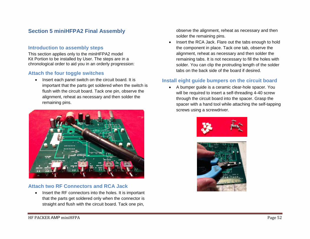
HF PACKER AMP miniHFPA Page 52
Section 5 miniHFPA2 Final Assembly
Introduction to assembly steps This section applies only to the miniHFPA2 model Kit Portion to be installed by User. The steps are in a chronological order to aid you in an orderly progression:
Attach the four toggle switches • Insert each panel switch on the circuit board. It is
important that the parts get soldered when the switch is flush with the circuit board. Tack one pin, observe the alignment, reheat as necessary and then solder the remaining pins.
Attach two RF Connectors and RCA Jack • Insert the RF connectors into the holes. It is important
that the parts get soldered only when the connector is straight and flush with the circuit board. Tack one pin,
observe the alignment, reheat as necessary and then solder the remaining pins.
• Insert the RCA Jack. Flare out the tabs enough to hold the component in place. Tack one tab, observe the alignment, reheat as necessary and then solder the remaining tabs. It is not necessary to fill the holes with solder. You can clip the protruding length of the solder tabs on the back side of the board if desired.
Install eight guide bumpers on the circuit board • A bumper guide is a ceramic clear-hole spacer. You
will be required to insert a self-threading 4-40 screw through the circuit board into the spacer. Grasp the spacer with a hand tool while attaching the self-tapping screws using a screwdriver.

HF PACKER AMP miniHFPA Page 53
Bottom Cover Assembly The bottom cover has the holes for the connectors on end.
• Install four Rubber Bumpers. You will need small hand tool pliers and a tiny screwdriver for this assembly. Locate the four black rubber bumpers. On the outside of the bottom cover, insert the rubber bumpers one at a time through the four corner holes. You will find it difficult to do unless you use a technique to get the rubber through the hole. A tiny blade screwdriver can be used to push the rubber into and through the hole while you are pressing down with your thumb on the bumper head.
• Place the bumper on the hole and press firmly down with the thumb.
• With a tiny screwdriver or equivalent, push in on the side of the rubber that is not going into the hole. You may have to work around the perimeter pressing the rubber into the hole while maintaining pressure on the bumper head.
• Once you start seeing some rubber passing through the hole. After you get about 1/8th inch passing through the hole, you can use small hand tool pliers to grasp the rubber and pull the rubber further through the hole. You will have to tug in all lateral directions to make the rubber enter the hole.
• Pull and work the rubber until the rubber bumper body is flush with the bottom of the bottom cover.
Attaching the Heat Sink Plate to the Case Top
Hardware Mounting Reference
1 One each 6-32 standoff with four washers 2 Four each 4-40 standoff with two washers 3 Four every 4-40 screws with one washer 4 Two each ceramic washer with two each 6-32 nylon cap head screws and two MOSFETs
Apply a thin layer of thermal grease to the two ceramic washers
• Thinly coat the ceramic washers on both sides with the thermal grease.

HF PACKER AMP miniHFPA Page 54
Apply a thin layer of thermal grease to the heat sink plate where the ceramic washers and MOSFETs will attach
• Spread a thin layer of the thermal grease on the metal surfaces of the MOSFETs that will come into contact with the thermal washers when the MOSFETs are attached to the heat sink plate.
Attach the two ceramic washers to the heat sink plate
• Use two extra 6-32 x ¼ inch screws to hold in place the ceramic washers before attaching the MOSFETs to the heat sink plate. These two temporary screws hold the washers in a position allowing time for the pieces to set until it is time for the circuit board MOSFETs to be permanently attached to the plate.
Attach threaded standoff spacers • Each of the four 4-40 threaded spacers requires two
washers on the threads to make the inserted threads flush with the top of the heat sink plate.
• The one 6-32 threaded spacer requires three washers on the threads to make the inserted threads flush with the top of the heat sink plate.
• Remove the two temporary 6-32 screws from the ceramic washers. Do not disturb the position of the thermal washers so the position will stay in place.
Attach the heat sink plate to the case with mounting hardware
• Align the heat sink plate with the top of the case. Attach the plate to the case with four 4-40 screws. Each screw has two washers to ensure the threads do not protrude through the top of the heat sink plate.
Insert the completed circuit board into the top portion of the case.

HF PACKER AMP miniHFPA Page 55
• The MOSFETs must align over the ceramic washers when installed. You will adjust the position of the MOSFETs on the circuit board so that the holes in each MOSFET align with the ceramic washer holes now in position on the heat sink plate. Start by visual inspection through the access hole and pushing the MOSFET body to roughly align the MOSFET hole to be in the center of the access hole.
• Insert the switch end of the circuit board through the holes of the case top.
• As you position the circuit board, guide the circuit board to insert the top of the 6-32 threaded spacer through the access hole at U4.
• There may be a bit of resistance to get that spacer top
into the U4 mounting hole. With some encouragement such as flexing the panel slightly, you will be successful. Observe that all of the spacers are in contact with the bottom of the circuit board. A good assembly will only occur if the 6-32 threaded spacer is in the U4 access hole.
• Place the finned heat sink mounting hole on top of the U4 mounting hole and attach both to the spacer with a 6-32 x ¼ inch screw.
• Attach the two MOSFETs to the heat sink plate ceramic washers with the two hex head nylon screws.
Use the L-wrench for this job. You may need to make micro adjustments to align the holes. Tighten snug.
• Attach four 4-40 x ¼ inch screws through the circuit board mounting holes to the four spacers from the heat sink plate that align with the circuit board holes.
• Visually affirm that the MOSFETs are flush mounted to the ceramic washers.
• Trim the excess length of nylon screws by cutting the threads flush with the top of the heat sink plate.
Insert the two LPF Modules of Choice into the right-angle header connectors, J5 and J6
• I prefer to plug in the 30/20M LPF into J5 and the 60/40M LPF into J6.
View of the LPF plugged into the circuit board.
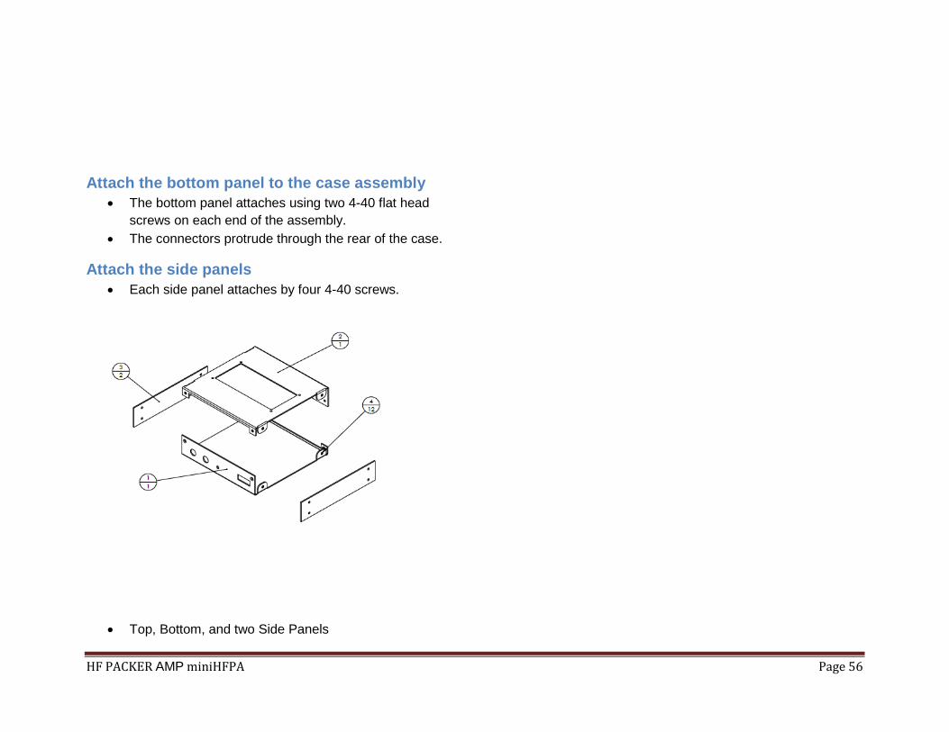
HF PACKER AMP miniHFPA Page 56
Attach the bottom panel to the case assembly • The bottom panel attaches using two 4-40 flat head
screws on each end of the assembly. • The connectors protrude through the rear of the case.
Attach the side panels • Each side panel attaches by four 4-40 screws.
• Top, Bottom, and two Side Panels

HF PACKER AMP miniHFPA Page 57
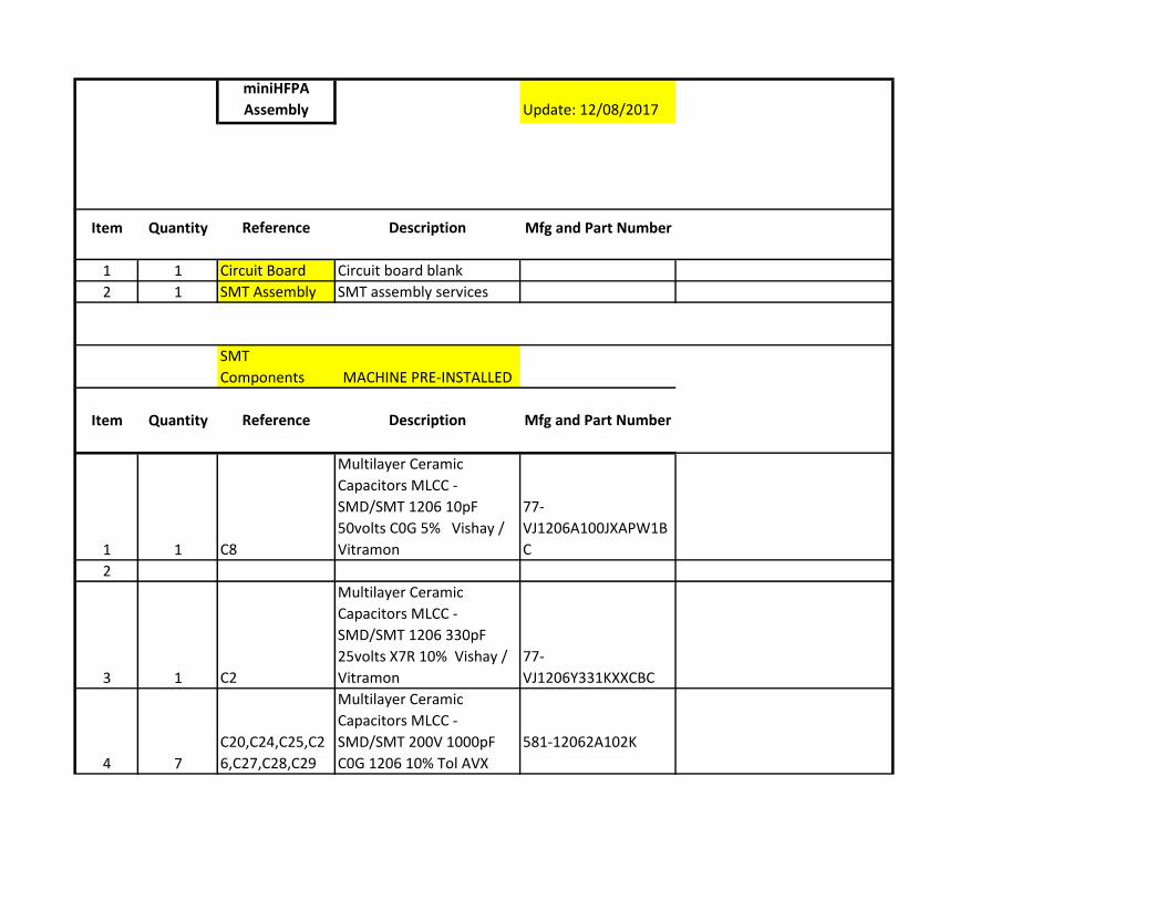
miniHFPA
Assembly Update: 12/08/2017
Item Quantity Reference Description Mfg and Part Number
1 1 Circuit Board Circuit board blank
2 1 SMT Assembly SMT assembly services
SMT
Components MACHINE PRE-INSTALLED
Item Quantity Reference Description Mfg and Part Number
1 1 C8
Multilayer Ceramic
Capacitors MLCC -
SMD/SMT 1206 10pF
50volts C0G 5% Vishay /
Vitramon
77-
VJ1206A100JXAPW1B
C
2
3 1 C2
Multilayer Ceramic
Capacitors MLCC -
SMD/SMT 1206 330pF
25volts X7R 10% Vishay /
Vitramon
77-
VJ1206Y331KXXCBC
4 7
C20,C24,C25,C2
6,C27,C28,C29
Multilayer Ceramic
Capacitors MLCC -
SMD/SMT 200V 1000pF
C0G 1206 10% Tol AVX
581-12062A102K
5 1 C1
Multilayer Ceramic
Capacitors MLCC -
SMD/SMT .01uF 50volts
10% X7R Vishay /
Vitramon
77-VJ1206Y103KXAAC
6 13
C3,C4,C6,C7,C9,
C10,C11,C13,C1
9,C12,C18,C22,C
23
80-C1206104K5RAC7867
C1206C104K5RAC7867
.1uF
Kemet Multilayer Ceramic
Capacitors MLCC -
SMD/SMT 80C-
C1206104K5RAC7867
7 1 C17
Multilayer Ceramic
Capacitors MLCC -
SMD/SMT 1.0uF 10V X7R
10%
603-
CC805KKX7R6BB105
case 0805
8 3 D1,D3,D7
Diodes - General Purpose,
Power, Switching
IO=150mA VR=75V HIGH
SPEED
Bournes: 652-CD1206-
S01575
9 4 D2,D6,D8,D9
Diodes - 100V, 1A S1BB--
13F
Diodes, Inc 621-S1BB-
F
10 1 F1
Resettable Fuses - PPTC
.75A 13.2V 100A Imax 650-MINISMDC075F-2
11 4 Q3,Q7,Q8,Q9
Bipolar Transistors - BJT
SOT-23 NPN GEN PUR
512-MMBT3904
Fairchild
12 2 Q5,Q6
Bipolar Transistors - BJT
PNP General Purpose
512-MMBT3906
Fairchild
13 10
R5,R11,R16,R17,
R23,R27,R30,R3
1,R34,R35
Resistor, Thin Film
Resistors - SMD 1/4W 1K
ohm 1% 50ppmYageo:
RT1206FRE071KL
14 1 R19
Thin Film Resistors - SMD
1/4W 1.2K ohm 1% 50ppm
Yageo:
RT1206FRE071K2L
15 2 R36, R37
Thick Film Resistors - SMD
1/4watt 2.32Kohms 1%
Vishay 71-CRCW1206-
2.32K-E3
16 1 R24
Thick Film Resistors - SMD
1206 3Kohms 1% Tol AEC-
Q200
Panasonic 667-ERJ-
8ENF3001V
17 2 R13,R26
Thin Film Resistors - SMD
4.7K Ohm 1% 1/4W 200
Volts 50ppm
Yageo:
RT1206FRE074K7L
18 10
R4,R10,R12,R14,
R18,R22,R25,R2
8,R29,R32
Thin Film Resistors - SMD
1/4W 10K ohm 1% 50ppm
Yageo:
RT1206FRE0710KL
19 1 R15
Resistor, 27K Thin Film
Resistors - SMD
Yageo:
RT1206FRE0727KL
20 2 R33,R20
Thin Film Resistors - SMD
1/4W 100K ohm 1%
50ppm
Yageo:
RT1206FRE07100KL
21 1 R21
Thin Film Resistors - SMD
1/4W 1M ohm 1% 50ppm
Yageo:
RT1206FRE071ML
22 1 R38
Thin Film Resistors - SMD
1/4W 47K ohm 1% 50ppm
Yageo:
RT1206FRE0747KL
23 1 U5
IC, Intellegent Power
Switch IPS511S Series 35V
135mOhm Fully Protected
High Side Power Mosfet
Switch D2PAK-5 IPS511S
24 1 U6 IC, Dual Schmidt Trigger 863-NL27WZ14DTT1G
25 1 U1
IC 3-TERM 0.1A 5V POS
REG 512-KA78L05AIMTF
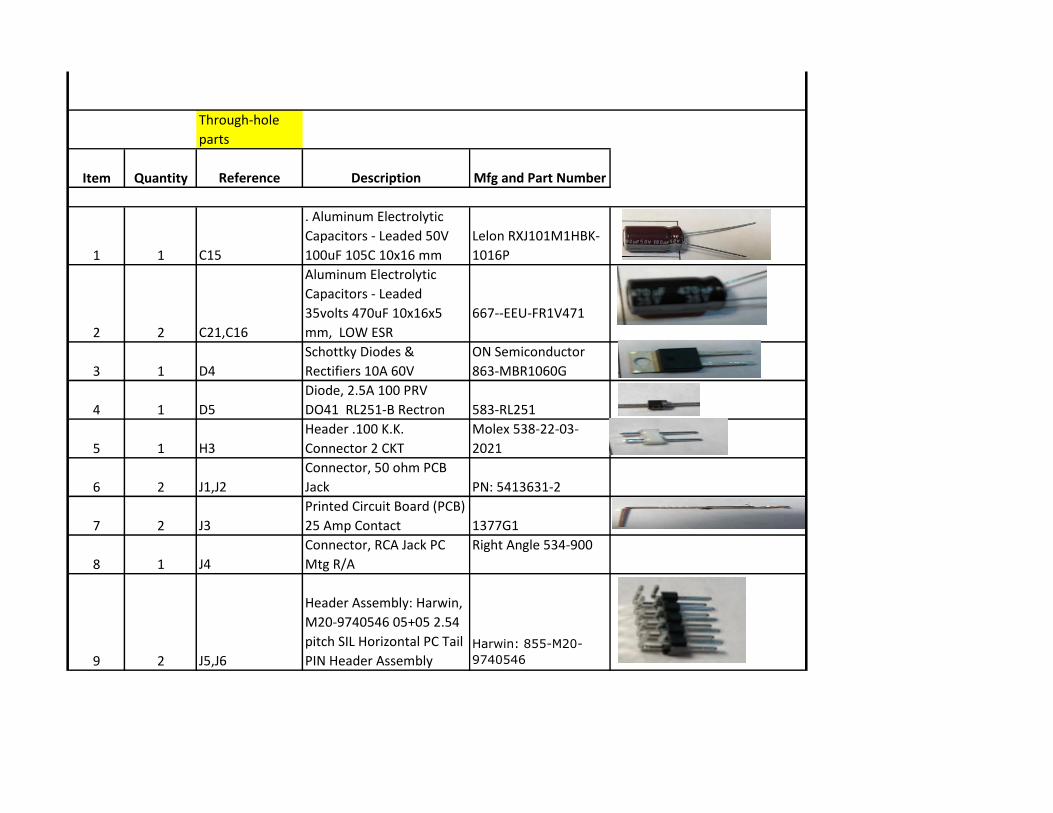
Through-hole
parts
Item Quantity Reference Description Mfg and Part Number
1 1 C15
. Aluminum Electrolytic
Capacitors - Leaded 50V
100uF 105C 10x16 mm
Lelon RXJ101M1HBK-
1016P
2 2 C21,C16
Aluminum Electrolytic
Capacitors - Leaded
35volts 470uF 10x16x5
mm, LOW ESR
667--EEU-FR1V471
3 1 D4
Schottky Diodes &
Rectifiers 10A 60V
ON Semiconductor
863-MBR1060G
4 1 D5
Diode, 2.5A 100 PRV
DO41 RL251-B Rectron 583-RL251
5 1 H3
Header .100 K.K.
Connector 2 CKT
Molex 538-22-03-
2021
6 2 J1,J2
Connector, 50 ohm PCB
Jack PN: 5413631-2
7 2 J3
Printed Circuit Board (PCB)
25 Amp Contact 1377G1
8 1 J4
Connector, RCA Jack PC
Mtg R/A
Right Angle 534-900
9 2 J5,J6
Header Assembly: Harwin,
M20-9740546 05+05 2.54
pitch SIL Horizontal PC Tail
PIN Header AssemblyHarwin: 855-M20-
9740546
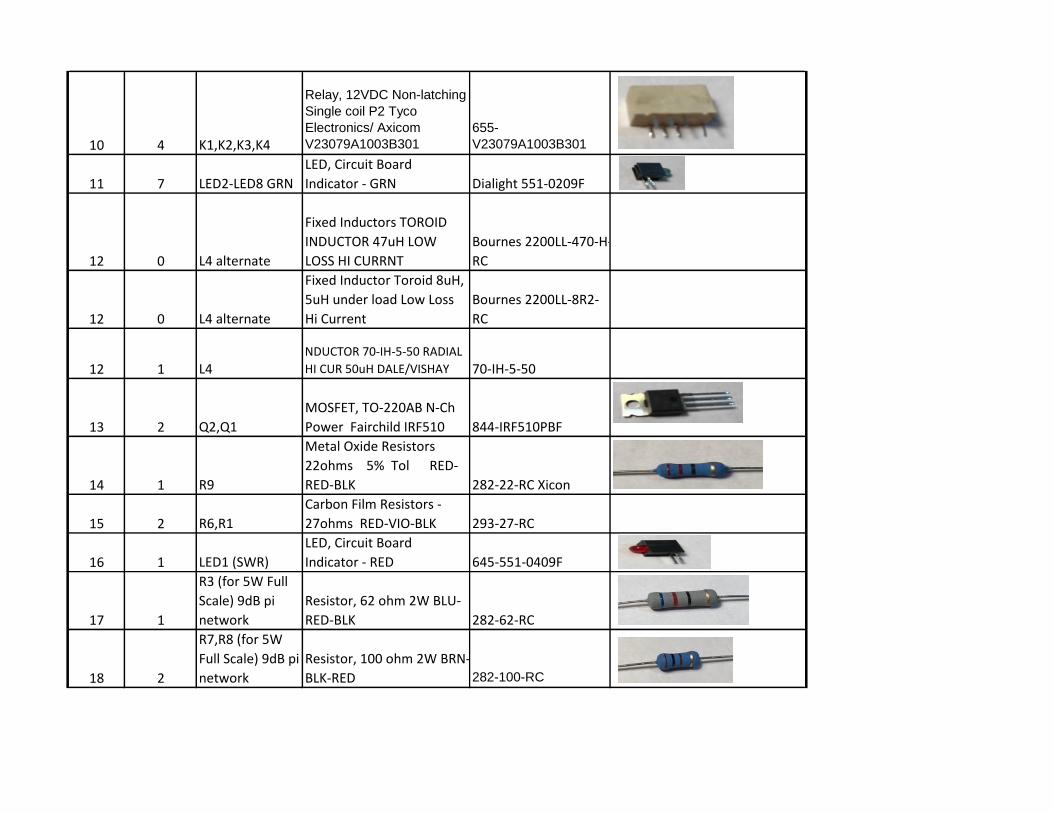
10 4 K1,K2,K3,K4
Relay, 12VDC Non-latching
Single coil P2 Tyco
Electronics/ Axicom
V23079A1003B301
655-
V23079A1003B301
11 7 LED2-LED8 GRN
LED, Circuit Board
Indicator - GRN Dialight 551-0209F
12 0 L4 alternate
Fixed Inductors TOROID
INDUCTOR 47uH LOW
LOSS HI CURRNT
Bournes 2200LL-470-H-
RC
12 0 L4 alternate
Fixed Inductor Toroid 8uH,
5uH under load Low Loss
Hi Current
Bournes 2200LL-8R2-
RC
12 1 L4NDUCTOR 70-IH-5-50 RADIAL
HI CUR 50uH DALE/VISHAY 70-IH-5-50
13 2 Q2,Q1
MOSFET, TO-220AB N-Ch
Power Fairchild IRF510 844-IRF510PBF
14 1 R9
Metal Oxide Resistors
22ohms 5% Tol RED-
RED-BLK 282-22-RC Xicon
15 2 R6,R1
Carbon Film Resistors -
27ohms RED-VIO-BLK 293-27-RC
16 1 LED1 (SWR)
LED, Circuit Board
Indicator - RED 645-551-0409F
17 1
R3 (for 5W Full
Scale) 9dB pi
network
Resistor, 62 ohm 2W BLU-
RED-BLK 282-62-RC
18 2
R7,R8 (for 5W
Full Scale) 9dB pi
network
Resistor, 100 ohm 2W BRN-
BLK-RED 282-100-RC
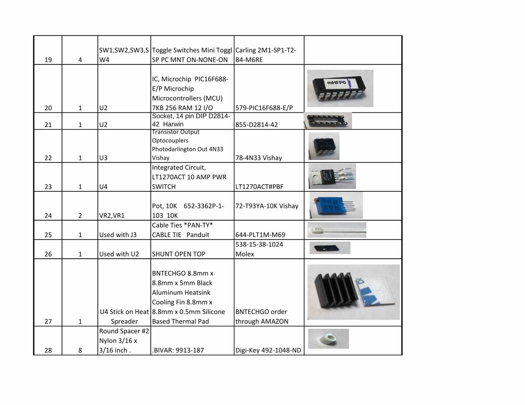
19 4
SW1,SW2,SW3,S
W4
Toggle Switches Mini Toggl
SP PC MNT ON-NONE-ON
Carling 2M1-SP1-T2-
B4-M6RE
20 1 U2
IC, Microchip PIC16F688-
E/P Microchip
Microcontrollers (MCU)
7KB 256 RAM 12 I/O 579-PIC16F688-E/P
21 1 U2Socket, 14 pin DIP D2814-
42 Harwin 855-D2814-42
22 1 U3
Transistor Output
Optocouplers
Photodarlington Out 4N33
Vishay 78-4N33 Vishay
23 1 U4
Integrated Circuit,
LT1270ACT 10 AMP PWR
SWITCH LT1270ACT#PBF
24 2 VR2,VR1
Pot, 10K 652-3362P-1-
103 10K
72-T93YA-10K Vishay
25 1 Used with J3
Cable Ties *PAN-TY*
CABLE TIE Panduit 644-PLT1M-M69
26 1 Used with U2 SHUNT OPEN TOP
538-15-38-1024
Molex
27 1
U4 Stick on Heat
Spreader
BNTECHGO 8.8mm x
8.8mm x 5mm Black
Aluminum Heatsink
Cooling Fin 8.8mm x
8.8mm x 0.5mm Silicone
Based Thermal Pad
BNTECHGO order
through AMAZON
28 8
Round Spacer #2
Nylon 3/16 x
3/16 inch . .BIVAR: 9913-187 Digi-Key 492-1048-ND
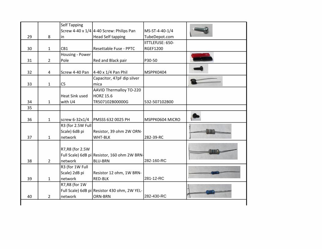
29 8
Self Tapping
Screw 4-40 x 1/4
in
4-40 Screw: Philips Pan
Head Self tapping
MS-ST-4-40-1/4
TubeDepot.com
30 1 CB1 Resettable Fuse - PPTC
lITTLEfUSE: 650-
RGEF1200
31 2
Housing - Power
Pole Red and Black pair P30-50
32 4 Screw 4-40 Pan 4-40 x 1/4 Pan Phil MSPPK0404
33 1 C5
Capacitor, 47pF dip silver
mica
34 1
Heat Sink used
with U4
AAVID Thermalloy TO-220
HORZ 15.6
TR507102B00000G 532-507102B00
35
36 1 screw 6-32x1/4 PMSSS 632 0025 PH MSPPK0604 MICRO
37 1
R3 (for 2.5W Full
Scale) 6dB pi
network
Resistor, 39 ohm 2W ORN-
WHT-BLK 282-39-RC
38 2
R7,R8 (for 2.5W
Full Scale) 6dB pi
network
Resistor, 160 ohm 2W BRN-
BLU-BRN 282-160-RC
39 1
R3 (for 1W Full
Scale) 2dB pi
network
Resistor 12 ohm, 1W BRN-
RED-BLK 281-12-RC
40 2
R7,R8 (for 1W
Full Scale) 6dB pi
network
Resistor 430 ohm, 2W YEL-
ORN-BRN 282-430-RC
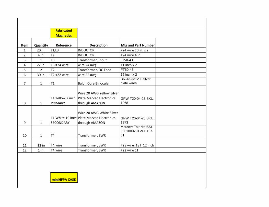
Fabricated
Magnetics
Item Quantity Reference Description Mfg and Part Number
1 20 in. L1,L3 INDUCTOR #24 wire 10 in. x 2
2 4 in. L2 INDUCTOR #24 wire 4 in
3 1 T3 Transformer, Input FT50-43 .
4 22 in. T3 #24 wire wire 24 awg 11 inch x 2
5 2 T2 Transformer, DC Feed FT50-43 .
6 30 in. T2 #22 wire wire 22 awg 15 inch x 2
7 1 T1 Balun Core BinocularBN-43-3312 + silver
plate wires
8 1
T1 Yellow 7 inch
PRIMARY
Wire 20 AWG Yellow Silver
Plate Marvec Electronics
through AMAZONGPW T20-04-25 SKU:
1968
9 1
T1 White 10 inch
SECONDARY
Wire 20 AWG White Silver
Plate Marvec Electronics
through AMAZONGPW T20-04-25 SKU:
1973
10 1 T4 Transformer, SWR
Mouser: Fair-rite 623-
5961000201 or FT37-
61
11 12 in T4 wire Transformer, SWR #28 wire 18T 12 inch
12 1 in. T4 wire Transformer, SWR #22 wire 1T
miniHFPA CASE
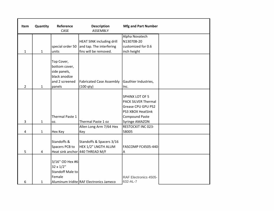
Item Quantity Reference Description Mfg and Part NumberCASE ASSEMBLY
1 1
special order 50
units
HEAT SINK including drill
and tap. The interfering
fins will be removed.
Alpha Novatech
N13070B-20
customized for 0.6
inch height
2 1
Top Cover,
bottom cover,
side panels,
black anodize
and 2 screened
panels
Fabricated Case Assembly
(100 qty)
Gauthier Industries,
Inc.
3 1
Thermal Paste 1
oz. Thermal Paste 1 oz
SPHINX LOT OF 5
PACK SILVER Thermal
Grease CPU GPU PS2
PS3 XBOX HeatSink
Compound Paste
Syringe AMAZON
4 1 Hex Key
Allen Long Arm 7/64 Hex
Key
RESTOCKIT INC 023-
58005
5 4
Standoffs &
Spacers PCB to
Heat sink anchor
Standoffs & Spacers 3/16
HEX 1/2" LNGTH ALUM
440 THREAD M/F
FASCOMP FC4505-440-
A
6 1
3/16'' OD Hex #6-
32 x 1/2''
Standoff Male to
Female
Aluminum Iridite RAF Electronics JamecoRAF Electronics 4505-
632-AL-7
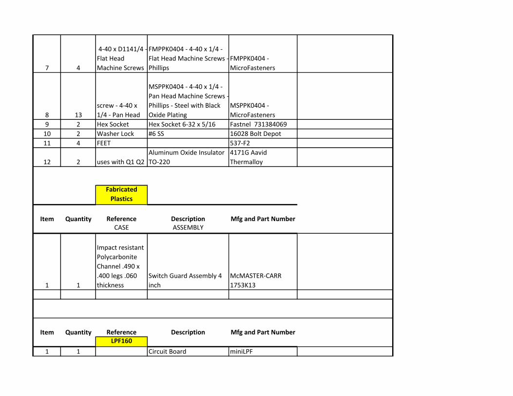
7 4
4-40 x D1141/4 -
Flat Head
Machine Screws
FMPPK0404 - 4-40 x 1/4 -
Flat Head Machine Screws -
Phillips
FMPPK0404 -
MicroFasteners
8 13
screw - 4-40 x
1/4 - Pan Head
MSPPK0404 - 4-40 x 1/4 -
Pan Head Machine Screws -
Phillips - Steel with Black
Oxide Plating
MSPPK0404 -
MicroFasteners
9 2 Hex Socket Hex Socket 6-32 x 5/16 Fastnel 731384069
10 2 Washer Lock #6 SS 16028 Bolt Depot
11 4 FEET 537-F2
12 2 uses with Q1 Q2
Aluminum Oxide Insulator
TO-220
4171G Aavid
Thermalloy
Fabricated
Plastics
Item Quantity Reference Description Mfg and Part NumberCASE ASSEMBLY
1 1
Impact resistant
Polycarbonite
Channel .490 x
.400 legs .060
thickness
Switch Guard Assembly 4
inch
McMASTER-CARR
1753K13
Item Quantity Reference Description Mfg and Part NumberLPF160
1 1 Circuit Board miniLPF
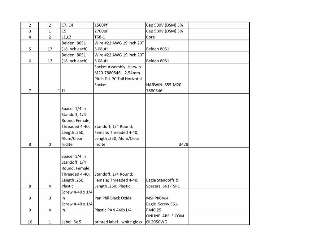
2 2 C7, C4 1500Pf Cap 500V (DSM) 5%
3 1 C5 2700pF Cap 500V (DSM) 5%
4 2 L1,L2 T68-1 Core
5 17
Belden: 8051
(18 inch each)
Wire #22 AWG 19 inch 20T
5.08uH Belden 8051
6 17
Belden: 8051
(18 inch each)
Wire #22 AWG 19 inch 20T
5.08uH Belden 8051
7 1 J1
Socket Assembly: Harwin
M20-7880546L 2.54mm
Pitch DIL PC Tail Horizotal
Socket HARWIN: 855-M20-
7880546
8 0
Spacer 1/4 in
Standoff; 1/4
Round; Female;
Threaded 4-40;
Length .250;
Alum/Clear
Iridite
Standoff; 1/4 Round;
Female; Threaded 4-40;
Length .250; Alum/Clear
Iridite 3478
8 4
Spacer 1/4 in
Standoff; 1/4
Round; Female;
Threaded 4-40;
Length .250;
Plastic
Standoff; 1/4 Round;
Female; Threaded 4-40;
Length .250; Plastic
Eagle Standoffs &
Spacers, 561-TSP1
9 0
Screw 4-40 x 1/4
in Pan Phil Black Oxide MSPPK0404
9 4
Screw 4-40 x 1/4
in Plastic PAN 440x1/4
Eagle Screw 561-
P440.25
10 1 Label .5x.5 printed label - white gloss
ONLINELABELS.COM
OL2050WG
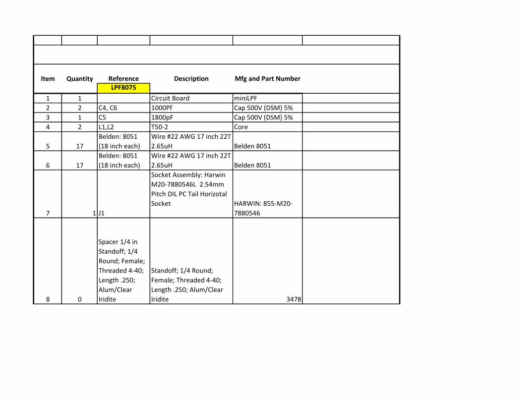
Item Quantity Reference Description Mfg and Part NumberLPF8075
1 1 Circuit Board miniLPF
2 2 C4, C6 1000Pf Cap 500V (DSM) 5%
3 1 C5 1800pF Cap 500V (DSM) 5%
4 2 L1,L2 T50-2 Core
5 17
Belden: 8051
(18 inch each)
Wire #22 AWG 17 inch 22T
2.65uH Belden 8051
6 17
Belden: 8051
(18 inch each)
Wire #22 AWG 17 inch 22T
2.65uH Belden 8051
7 1 J1
Socket Assembly: Harwin
M20-7880546L 2.54mm
Pitch DIL PC Tail Horizotal
Socket HARWIN: 855-M20-
7880546
8 0
Spacer 1/4 in
Standoff; 1/4
Round; Female;
Threaded 4-40;
Length .250;
Alum/Clear
Iridite
Standoff; 1/4 Round;
Female; Threaded 4-40;
Length .250; Alum/Clear
Iridite 3478
8 4
Spacer 1/4 in
Standoff; 1/4
Round; Female;
Threaded 4-40;
Length .250;
Plastic
Standoff; 1/4 Round;
Female; Threaded 4-40;
Length .250; Plastic
Eagle Standoffs &
Spacers, 561-TSP1
9 0
Screw 4-40 x 1/4
in Pan Phil Black Oxide MSPPK0404
9 4
Screw 4-40 x 1/4
in Plastic PAN 440x1/4
Eagle Screw 561-
P440.25
10 1 Label .5x.5 printed label - white gloss
ONLINELABELS.COM
OL2050WG
Item Quantity Reference Description Mfg and Part NumberLPF6040
1 1 Circuit Board miniLPF
2 1 C1 39pF Cap 500V (DSM) 5%
3 1 C2 110pF Cap 500V (DSM) 5%
4 1 C4 390pF Cap 500V (DSM) 5%
5 1 C5 680pF Cap 500V (DSM) 5%
6 1 C6 330pF Cap 500V (DSM) 5%
7 2 L1,L2 T50-2 (RED)
Core T50-2 (Red)
PartsAndKits
8 13
Belden: 8051
(13 inch)
Wire # 22 AWG 13 inch,
15T: 0.37uH Belden 8051
9 12
Belden: 8051
(12 inch )
Wire # 22 AWG 12 inch,
13T: 0.17uH Belden 8051
10 1 J1
Socket Assembly: Harwin
M20-7880546L 2.54mm
Pitch DIL PC Tail Horizotal
Socket HARWIN: 855-M20-
7880546
11 0
Spacer 1/4 x 4-
40 alum.
.25 x .25 alum round
threaded spacer 4-40 Keystone 534-3478
11 4
Spacer 1/4 in
Standoff; 1/4
Round; Female;
Threaded 4-40;
Length .250;
Plastic
Standoff; 1/4 Round;
Female; Threaded 4-40;
Length .250; Plastic
Eagle Standoffs &
Spacers, 561-TSP1
12 0
Screw 4-40 x 1/4
in Pan Phil Black Oxide MSPPK0404
12 4
Screw 4-40 x 1/4
in Plastic PAN 440x1/4
Eagle Screw 561-
P440.25
13 1 Label .5x.5 printed label - white gloss
ONLINELABELS.COM
OL2050WG
Item Quantity Reference Description Mfg and Part NumberLPF3020
1 1 Circuit Board miniLPF
2 1 C1 27pF Cap 500V (DSM) 5%
3 1 C3 120pF Cap 500V (DSM) 5%
3 1 C4 100pF Cap 500V (DSM) 5%
4 1 C2 150pF Cap 500V (DSM) 5%
5 2 C5,C6 220pF Cap 500V (DSM) 5%
6 1 C7 47pF Cap 500V (DSM) 5%
7 10
L1 Belden 8051
(11 inches each) Wire # 22 AWG 10T Belden 8051
8 10
L2 Belden 8051
(11 inches each) Wire # 22 AWG 9T Belden 8051
9 10
L3 Belden 8051
(11 inches each) Wire # 22 AWG 10T Belden 8051
10 3 L1,L2,L3 T50-10 (Black)
Core T50-10 (Black)
PartsAndKits
11 1 J1
Socket Assembly: Harwin
M20-7880546L 2.54mm
Pitch DIL PC Tail Horizotal
Socket HARWIN: 855-M20-
7880546
12 0
Spacer 1/4 x 4-
40 alum.
.25 x .25 alum round
threaded spacer 4-40 Keystone 534-3478
12 4
Spacer 1/4 in
Standoff; 1/4
Round; Female;
Threaded 4-40;
Length .250;
Plastic
Standoff; 1/4 Round;
Female; Threaded 4-40;
Length .250; Plastic
Eagle Standoffs &
Spacers, 561-TSP1
13 0
Screw 4-40 x 1/4
in Pan Phil Black Oxide MSPPK0404
13 4
Screw 4-40 x 1/4
in Plastic PAN 440x1/4
Eagle Screw 561-
P440.25
14 1 Label .5x.5 printed label - white gloss
ONLINELABELS.COM
OL2050WG
Item Quantity Reference Description Mfg and Part NumberLPF1715
1 1 Circuit Board miniLPF (qty=200)
2 1 C1 12pF Cap 500V (DSM) 5%
3 1 C2 39pF Cap 500V (DSM) 5%
4 1 C4 150pF Cap 500V (DSM) 5%
5 1 C5 220pF Cap 500V (DSM) 5%
6 1 C6 100pF Cap 500V (DSM) 5%
7 10
Belden 8051 (10
inches each)
Wire # 22 AWG 11T
0.47uH Belden 8051
8 10
Belden 8051 (10
inches each)
Wire # 22 AWG 10T
0.43uH Belden 8051
9 2 L1,L2 T50-10 (Black) Core: T50-10 (Black)
10 1 J1
Socket Assembly: Harwin
M20-7880546L 2.54mm
Pitch DIL PC Tail Horizotal
Socket HARWIN: 855-M20-
7880546
11 0
Spacer 1/4 x 4-
40 alum.
.25 x .25 alum round
threaded spacer 4-40 Keystone 534-3478
11 4
Spacer 1/4 in
Standoff; 1/4
Round; Female;
Threaded 4-40;
Length .250;
Plastic
Standoff; 1/4 Round;
Female; Threaded 4-40;
Length .250; Plastic
Eagle Standoffs &
Spacers, 561-TSP1
12 0
Screw 4-40 x 1/4
in Pan Phil Black Oxide MSPPK0404
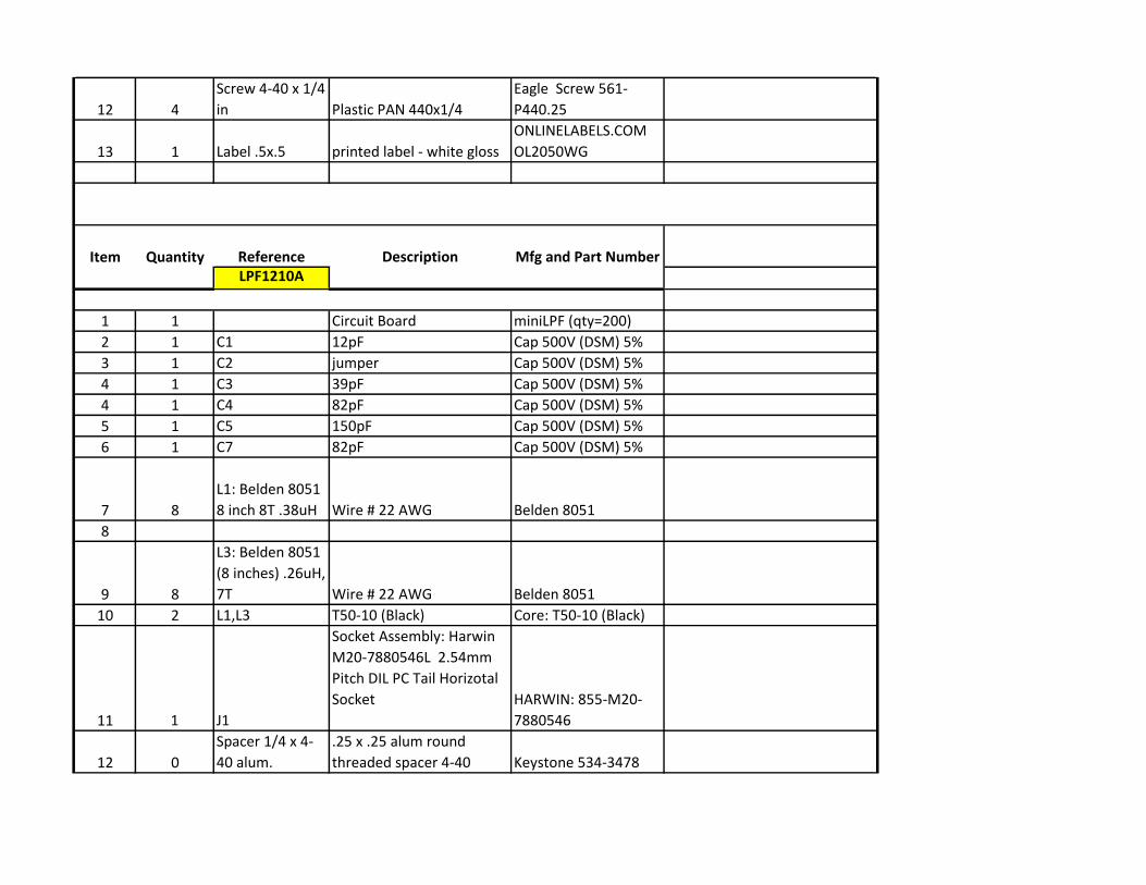
12 4
Screw 4-40 x 1/4
in Plastic PAN 440x1/4
Eagle Screw 561-
P440.25
13 1 Label .5x.5 printed label - white gloss
ONLINELABELS.COM
OL2050WG
Item Quantity Reference Description Mfg and Part NumberLPF1210A
1 1 Circuit Board miniLPF (qty=200)
2 1 C1 12pF Cap 500V (DSM) 5%
3 1 C2 jumper Cap 500V (DSM) 5%
4 1 C3 39pF Cap 500V (DSM) 5%
4 1 C4 82pF Cap 500V (DSM) 5%
5 1 C5 150pF Cap 500V (DSM) 5%
6 1 C7 82pF Cap 500V (DSM) 5%
7 8
L1: Belden 8051
8 inch 8T .38uH Wire # 22 AWG Belden 8051
8
9 8
L3: Belden 8051
(8 inches) .26uH,
7T Wire # 22 AWG Belden 8051
10 2 L1,L3 T50-10 (Black) Core: T50-10 (Black)
11 1 J1
Socket Assembly: Harwin
M20-7880546L 2.54mm
Pitch DIL PC Tail Horizotal
Socket HARWIN: 855-M20-
7880546
12 0
Spacer 1/4 x 4-
40 alum.
.25 x .25 alum round
threaded spacer 4-40 Keystone 534-3478
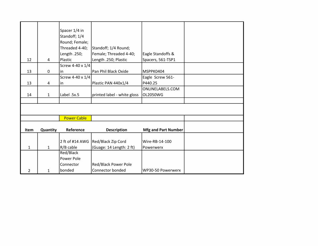
12 4
Spacer 1/4 in
Standoff; 1/4
Round; Female;
Threaded 4-40;
Length .250;
Plastic
Standoff; 1/4 Round;
Female; Threaded 4-40;
Length .250; Plastic
Eagle Standoffs &
Spacers, 561-TSP1
13 0
Screw 4-40 x 1/4
in Pan Phil Black Oxide MSPPK0404
13 4
Screw 4-40 x 1/4
in Plastic PAN 440x1/4
Eagle Screw 561-
P440.25
14 1 Label .5x.5 printed label - white gloss
ONLINELABELS.COM
OL2050WG
Power Cable
Item Quantity Reference Description Mfg and Part Number
1 1
2 ft of #14 AWG
R/B cable
Red/Black Zip Cord
(Guage: 14 Length: 2 ft)
Wire-RB-14-100
Powerwerx
2 1
Red/Black
Power Pole
Connector
bonded
Red/Black Power Pole
Connector bonded WP30-50 Powerwerx
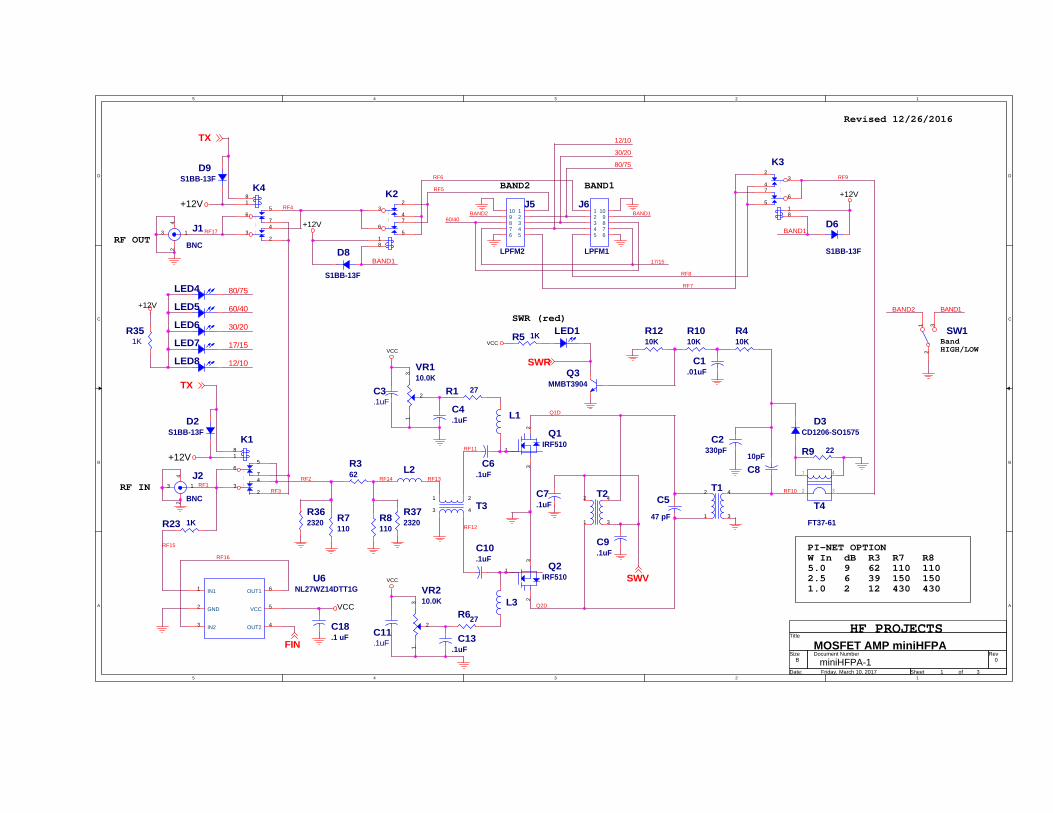
5
5
4
4
3
3
2
2
1
1
D D
C C
B B
A A
HF PROJECTS
RF IN
SWR (red)
BandHIGH/LOW
2 3
41
RF OUT
BAND1BAND2
PI-NET OPTIONW In dB R3 R7 R85.0 9 62 110 1102.5 6 39 150 1501.0 2 12 430 430
Revised 12/26/2016
miniHFPA-1 0
MOSFET AMP miniHFPAB
1 3Friday, March 10, 2017
Title
Size Document Number Rev
Date: Sheet of
RF11
Q1D
RF1
RF12
RF15
RF13
RF16
RF2 RF14
Q2D
RF10
RF9
BAND2 BAND1
RF3
RF4
BAND1
RF17 BAND1
12/10
30/20
80/75
80/75
30/20
12/10
60/40
RF5
BAND2 BAND1
17/15
60/40
RF6
RF8
RF7
17/15
SWR
FIN
SWV
TX
TX
VCC
VCCVCC
VCC
+12V
+12V
+12V
+12V
+12V
T31
3
2
4
T2
1 3
2 4
L3
T1
1 3
2 4
Q2IRF510
2
1
3
C6.1uF
VR210.0K
13
2
VR110.0K
13
2
L1
R627
C11.1uF
C3.1uF
C7.1uF
L2
C9.1uF
R1 27
Q1IRF510
2
1
3
C13.1uF
C547 pF
R362
R7110
R8110
C10.1uF
C4.1uF
J5
LPFM2
123456
78910
C810pF
K1
32
4
67
518
C2330pF
T4FT37-61
J1BNC
1
2
3
4
Q3MMBT3904
C18.1 uF
J6
LPFM1
12345 6
789
10
D6
S1BB-13F
K33
2
4
67
518
C1.01uF
R410K
R1010K
R1210K
R23 1K
LED1
R372320
R362320
R5 1K
K4
32
4
67
518
U6NL27WZ14DTT1G1 6
3 4
52
IN1 OUT1
IN2 OUT2
VCCGND
K23
2
4
67
518
D8
S1BB-13F
D2S1BB-13F
SW1
21 3
D3CD1206-SO1575
J2
BNC1
2
3
4
LED7
LED6
LED5
LED4
LED8
R351K
R9 22
D9S1BB-13F
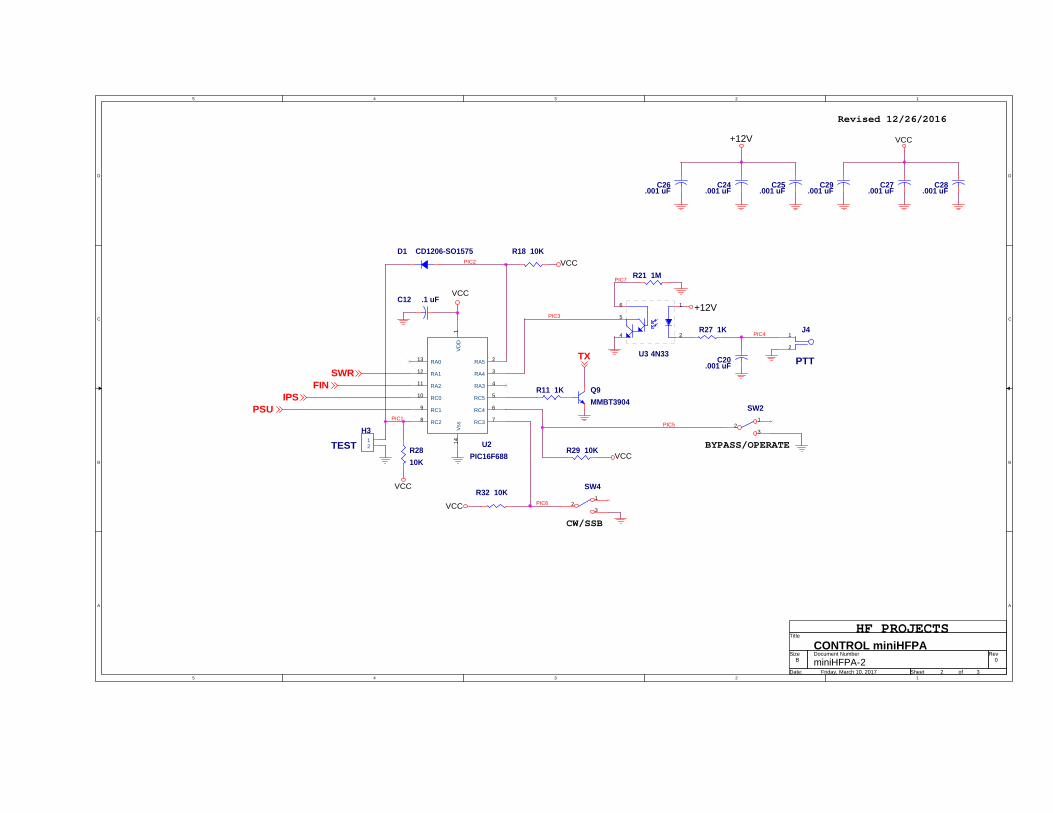
5
5
4
4
3
3
2
2
1
1
D D
C C
B B
A A
HF PROJECTS
BYPASS/OPERATE
CW/SSB
Revised 12/26/2016
miniHFPA-2 0
CONTROL miniHFPAB
2 3Friday, March 10, 2017
Title
Size Document Number Rev
Date: Sheet of
PIC7
PIC3
PIC1
PIC2
PIC5
PIC6
PIC4
TX
IPSPSU
SWRFIN
VCC
+12V
VCC
VCC
VCC
VCC
+12V VCC
Q9MMBT3904
R11 1K
R21 1M
U3 4N33
16
2
5
4R27 1K
C20.001 uF
C12 .1 uF
C26.001 uF
C24.001 uF
C25.001 uF
C29.001 uF
C27.001 uF
C28.001 uF
R2810K
R18 10KD1 CD1206-SO1575
J4
PTT
1
2
SW4
21
3
SW2
21
3
R29 10KU2
PIC16F688
5
2
3
4
14
6
78
9
10
11
12
13
1
RC5
RA5
RA4
RA3
Vss
RC4
RC3RC2
RC1
RC0
RA2
RA1
RA0
VDD
H3
TEST 12
R32 10K
5
5
4
4
3
3
2
2
1
1
D D
C C
B B
A A
HF PROJECTS
+-
(RED)TX
PWR (grn)
STANDBY/ON
(SOURCE)
(SOURCE)
OFF
ON
miniHFPA-3 0
PSU miniHFPAB
3 3Friday, March 10, 2017
Title
Size Document Number Rev
Date: Sheet of
PWR7
PWR10 VSW2
PWR6
PWR8
PWR2
PWR4
PWR5
PWR9
PWR1
PWR3
SWV
PSU
IPS
VCC
+12V
+12V
VCC
VCC
J3
PowerPole
12
R38 47K
Q5MMBT3906
C22.1 uF
C23.1 uF
U1KA78L05AIMTF3
21VIN
GN
D VOUT
R1410K
R161K
LED2
R341K
Q7MMBT3904
R33100K
CB1
D5RL251
L4 50 uH
+
C21330uF
U5IPS511S
1
23
45
GROUND
INVC
C
DG
OU
T
R171K
D7
CD1206-SO1575
U4LT1270A
1
2
3
45
VC
FB GN
D
VSWVIN
D4MBR1060G
3 1
+ C171uF
Q6MMBT3906
+
C15
100uF
R243K
R30 1K
R20 100K
R191.2K
R1527K
+
C16330uF
C19.1uF
F1MINISMD075F-2
R22 10K
R25 10K
SW3
21
3
LED3TX
Q8MMBT3904
R134.7K
R264.7K
R31 1K
5
5
4
4
3
3
2
2
1
1
D D
C C
B B
A A
20.5MHz
30/20 Value shown as reference
24MHz
HF PROJECTS
LPF3020, jumper 3-6 JP1L1:T50-10 580nH, 40.2MHz, 10TL2:T50-10 =400nH, 20.5MHz, 9TL3:T50-10 =430nH, 24.4MHz, 10TC1=27pF, C2=150pF, C3=120pF, C4=100pF, C5=220pF, C6=220pF,C7=47pF8 inch x 3 Belden 8051
LPF6040, jumper 2-6 JP1L1:T50-2=1.37uH, 21.8MHz, 15T 13 in.L2:T50-2=1.17uH, 14.0MHz, 13T 12 in.L3=0 ohmC1=39pF, C2=110pF, C3=openC4=390pF, C5L=680pF, C6=330pF, C7=open12 inch x 2 Belden 8051
LPF1715, jumper 4-6 JP1L1:T50-10 =470nH, 67MHz, 11TL2=openL3:T50-10 =430uH, 37.2MHz, 10TC1=12pF, C2=jumper, C3=47pfC4=120pF, C5=220pF, C6=open, C7=1008 inch x 2 Belden 8051
LPF8075, jumper 1-6 JP1L1:T68-6=2.65uH, 21T , L2=0 ohmL3:T68-6=2.65uH, 21T, C1=open, C2=open, C3=openC4L=1000pF, C5L=1800, C6=open, C7L=1000pF17 inch x 2 Belden 8051
JP1 Programming:Insert wire jumper betweenpin 6 and another pad toset the board identitySee Build List
40.2MHz
revised 4/23/2017BUILD LIST
LPF160, jumper none JP1 L1:T68-2=5.08uH, 28T , L2=openL3:T68-2=5.08uH, 28T, C1=open, C2=jumper, C3=openC4L=1500pF, C5L=2700, C6=open, C7L=1500pF23 inch x 2 Belden 8051
LPF1210, jumper 5-6 JP1L1:T50-10 =380nH, 67.2MHz, 8T 9in.L2:T50-10=330nH, 44.8MHz, 7T 8in.L3= T50-10=330nH 53.5 MHz, 7T 8in.C1=18pF, C2=47pF, C3=33pFC4=68pF, C5=150pF, C6=150pF, C7= 82pF7 inch x 2 Belden 8051
After 3/28/17 use the "A" versionLPF1210A, jumper 5-6 JP1L1:T50-10 =360nH, 8T 9in.L2:openL3= T50-10=230nH, 7T 8in.C1=12pF, C2=jumper, C3=39pFC4=82pF, C5=150pF, C6=open, C7= 68pF7 inch x 2 Belden 8051
4/8/17: Changed 160M to T68-2 from T68-1and changed 80M to T68-6 cores.
4/23/17: Changed 17/15M C4 was 150pfC2 was 39pf, C6 was 100pf, C7 was open
<Doc> 0
miniLPF 30/20 MB
1 1Sunday, April 23, 2017
Title
Size Document Number Rev
Date: Sheet of
OUT
80/7530/2012/10
17/1560/40COM
60/4017/15COM
80/7530/2012/10IN
GNDGND
IN OUT
C747pF
C1 27pF
C4100pF
C2 150pF
L1 580nH
C6220pF
L3 430nHL2 400nH
C5220pF
C3 120pF
C5L
JP1
HEADER 6
123456
C7L
J1
CON10
12345 6
789
10
C4L
Power Switch Modification for miniHFPA Virgil Stamps K5OOR www.hfprojects.com
The second switch from the left (STBY/ON) has to have the toggle action reversed. To accomplish this, remove the right pin of the switch and installing a jumper. Cut the pin off at the switch base.
On the opposite side, extract the switch pin from the third hole on the right. Prepare a one inch length of hookup wire, tinning the wire ends.
Solder attach the wire to the left terminal and insert wire into hole and solder (where the right terminal was installed).
Fabricating T2 Detail Virgil Stamps 12/31/2017
1. T2 is the dual core T50-43 wound with two 15 inch lengths of #22 enamel wire (Belden 8051).
T2 Cores and wire positioned for winding. Short end on the left.
a. The wire is a single 30 inch length of wire folded in the center. Work with the wire so that the two ends are parallel and smooth the entire 15 inch length with the aid of a pair of needle nose pliars positioned at the center bend and then with the other hand pulling the leads to make them conform to be parallel and smooth.
b. Position the wire through the two cores so the short end is about 3 inches length. 2. It is important to keep the wires tight and parallel throughout the winding process in
order to complete a quality process. With the aid of the pliars, tug on each end to make the wires to lay down flat.
3. Loop the long end through the core one time to achieve the look in the photo below
T2 with one loop completed through the core. Pull the leads tight from both ends.

Wrap the long ends through the core. Pull tight for each loop. Avoid wire crossover.
Continue for 10 loops through the center. Separate the folded wire by clipping the end of the loop.
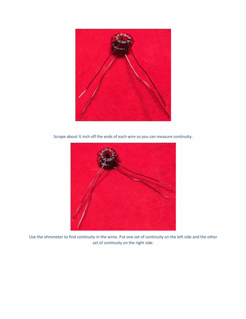
Scrape about ½ inch off the ends of each wire so you can measure continuity.
Use the ohmmeter to find continuity in the wires. Put one set of continuity on the left side and the other set of continuity on the right side.

Push the wires through the circuit board with winding 1 on the left and winding 2 on the right. Pull the leads tight from the back side to form the leads into the positions needed for final installation on the
circuit board. Clip the wires to about ½ inch length on the back side of the board.
T2 removed from circuit board after forming the leads for the final assembly. The next step is to remove the enamel from the ends of the wires and wet the leads with solder.
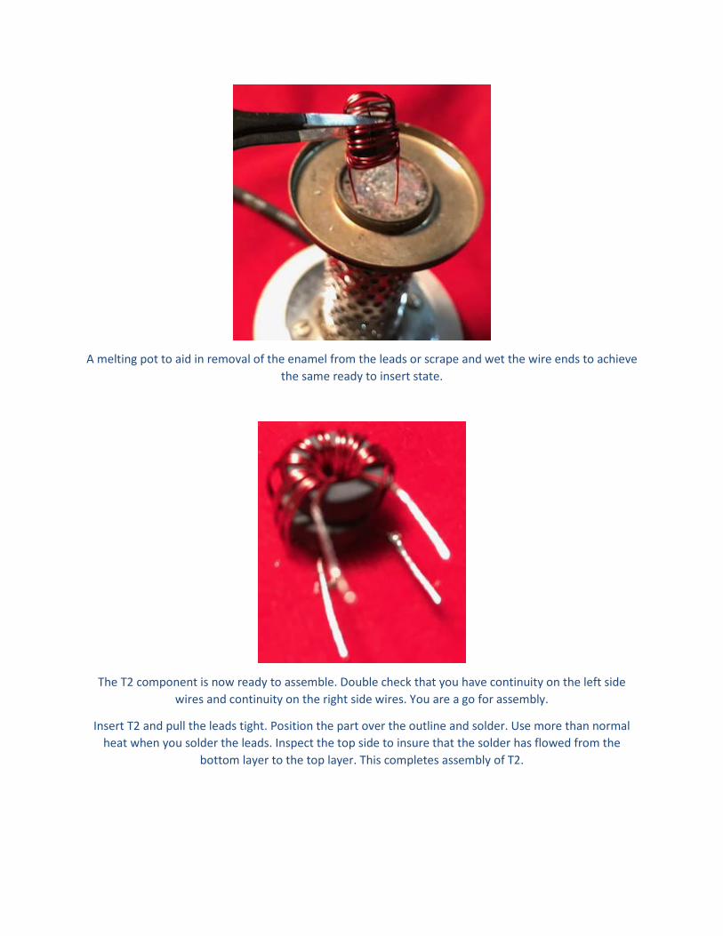
A melting pot to aid in removal of the enamel from the leads or scrape and wet the wire ends to achieve the same ready to insert state.
The T2 component is now ready to assemble. Double check that you have continuity on the left side wires and continuity on the right side wires. You are a go for assembly.
Insert T2 and pull the leads tight. Position the part over the outline and solder. Use more than normal heat when you solder the leads. Inspect the top side to insure that the solder has flowed from the
bottom layer to the top layer. This completes assembly of T2.
A
0.00
5.90
1.862.062.31
3.59
4.19
0.00 0.56 0.95 1.57 3.32 4.19 4.97 5.90
A = 6-32 tapall other holes = 4-40 tapDrill through and tap
HF PROJECTSVirgil Stamps [email protected]
A A3.00
(TOP)(bottom)
1/8 inch aluminum plateBlack Anodize Chamfer top edges (minimal)
from bottom
5.36
revised: 10/20/17
(LPF) (INLINE-BYPASS)(STBY/ON) (CCW SSB)
(PWR)(SWR) (TX)
0.7
0.0 6.0
0.0
0.65
1.3
5.3
5.00"
A A
SWITCH GUARD FRONT PANEL MOUNTINGHF PROJECTS3/31/2017
Measure and drill two 1/8th inch diameter holes in front panel at (A)

miniHFPA Power Out Testing
DC IN: 12.8V 11.2V BAND WATTS AMPS WATTS AMPS 160M 48.0 7.7 45 8.6 75M 50.0 8.6 45 8.9 40M 45.0 9 40 9.1 20M 40.0 8.3 39 9.9 17M 20.0 7.1 18 8.0 15M 22.0 7.2 20 7.7 12M 15.0 7.3 16 8.2 10M 18.0 5.6 18 6.5 Average 32.3 7.6 30.1 8.4
BLUE Series1 : DC In = 12.8V under load
Red Series2: DC In = 11.2V under load
0.0
10.0
20.0
30.0
40.0
50.0
60.0
160M 75M 40M 20M 17M 15M 12M 10M
Series1
Series2
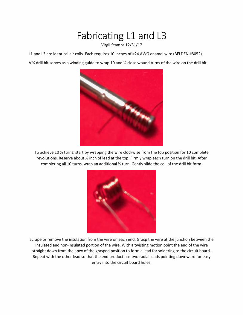
Fabricating L1 and L3 Virgil Stamps 12/31/17
L1 and L3 are identical air coils. Each requires 10 inches of #24 AWG enamel wire (BELDEN #8052)
A ¼ drill bit serves as a winding guide to wrap 10 and ½ close wound turns of the wire on the drill bit.
To achieve 10 ½ turns, start by wrapping the wire clockwise from the top position for 10 complete revolutions. Reserve about ½ inch of lead at the top. Firmly wrap each turn on the drill bit. After
completing all 10 turns, wrap an additional ½ turn. Gently slide the coil of the drill bit form.
Scrape or remove the insulation from the wire on each end. Grasp the wire at the junction between the insulated and non-insulated portion of the wire. With a twisting motion point the end of the wire
straight down from the apex of the grasped position to form a lead for soldering to the circuit board. Repeat with the other lead so that the end product has two radial leads pointing downward for easy
entry into the circuit board holes.

Shown here, the radial leads are inserted into the L1 location. The component is now snugged up to base of the circuit board. If the coil deforms slightly, use a ball point pen to align and compress the
inductor leads. Solder from the backside with enough heat to insure a solid connection from bottom to top of the circuit board. The component should be overlaying the silkscreen symbol.
The fabricated coils and transformers need to be soldered with confirmed connection. A poorly assembled inductor will give you nothing but grief.
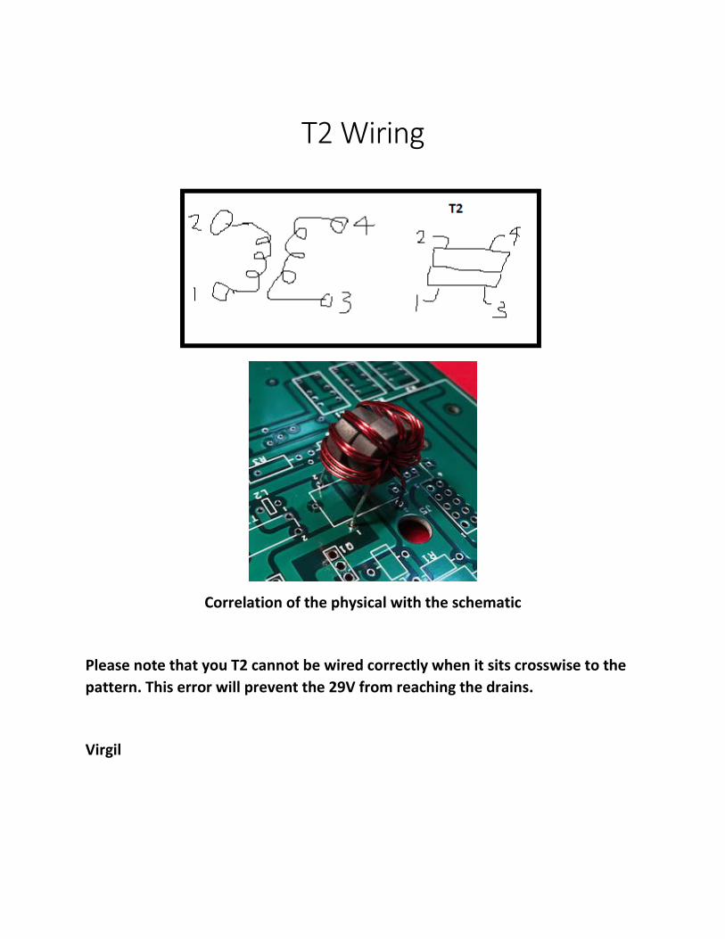
T2 Wiring
Correlation of the physical with the schematic
Please note that you T2 cannot be wired correctly when it sits crosswise to the pattern. This error will prevent the 29V from reaching the drains.
Virgil

Manual Changes 1 6 20181 Revised preliminary testing procedure2 Expanded detail assembly steps for magnetics3. added section 5

Flat Plate Heat Sink Information2 Virgil Stamps www.hfprojects 10 22 2017
Bottom of Plate with spacers and MOSFETs in place and attached to the top cover.
1 One each 6-32 standoff with four washers 2 Four each 4-40 standoff with two washers 3 Four each 4-40 screws with one washer 4 Two each ceramic washer with two each 6-32 nylon cap head screws and two MOSFETs 5 (not shown) Thermal grease to be used on the MOSFET metal base and both sides of the
ceramic spacers and the heat sink plate. Apply a thin even coat on all these surfaces.
The purpose of the spacers on the threads of the standoffs is to keep the threads from passing through the top of the heat sink plate.
The standoff (1) above requires four spacers so that the top of the spacer passes through the circuit board to facilitate heat sinking the LT1270ACT component to the case.
The threads of the nylon 6-32 hex head screw leave a ¼ inch length nub on the top side of the plate. You can cut these nylon screws flush, but it may make it difficult to use them again, once removed.
The MOSFETs illustrate how these components are mounted. The MOSFETs already installed are the exact spacing and can be reused.