Embed Size (px)
Citation preview
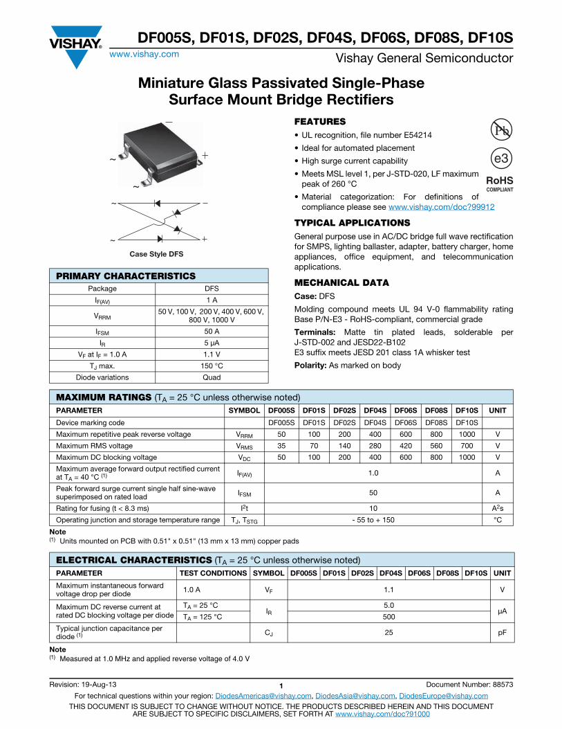
DF005S, DF01S, DF02S, DF04S, DF06S, DF08S, DF10Swww.vishay.com Vishay General Semiconductor
Revision: 19-Aug-13 1 Document Number: 88573
For technical questions within your region: [email protected], [email protected], [email protected] DOCUMENT IS SUBJECT TO CHANGE WITHOUT NOTICE. THE PRODUCTS DESCRIBED HEREIN AND THIS DOCUMENT
ARE SUBJECT TO SPECIFIC DISCLAIMERS, SET FORTH AT www.vishay.com/doc?91000
Miniature Glass Passivated Single-Phase Surface Mount Bridge Rectifiers
FEATURES• UL recognition, file number E54214
• Ideal for automated placement
• High surge current capability
• Meets MSL level 1, per J-STD-020, LF maximum peak of 260 °C
• Material categorization: For definitions of compliance please see www.vishay.com/doc?99912
TYPICAL APPLICATIONSGeneral purpose use in AC/DC bridge full wave rectification for SMPS, lighting ballaster, adapter, battery charger, home appliances, office equipment, and telecommunication applications.
MECHANICAL DATACase: DFS
Molding compound meets UL 94 V-0 flammability rating Base P/N-E3 - RoHS-compliant, commercial grade
Terminals: Matte tin plated leads, solderable per J-STD-002 and JESD22-B102E3 suffix meets JESD 201 class 1A whisker test
Polarity: As marked on body
Note(1) Units mounted on PCB with 0.51" x 0.51" (13 mm x 13 mm) copper pads
Note(1) Measured at 1.0 MHz and applied reverse voltage of 4.0 V
PRIMARY CHARACTERISTICSPackage DFS
IF(AV) 1 A
VRRM50 V, 100 V, 200 V, 400 V, 600 V,
800 V, 1000 V
IFSM 50 A
IR 5 μA
VF at IF = 1.0 A 1.1 V
TJ max. 150 °C
Diode variations Quad
~
~
Case Style DFS
~
~
MAXIMUM RATINGS (TA = 25 °C unless otherwise noted)PARAMETER SYMBOL DF005S DF01S DF02S DF04S DF06S DF08S DF10S UNIT
Device marking code DF005S DF01S DF02S DF04S DF06S DF08S DF10S
Maximum repetitive peak reverse voltage VRRM 50 100 200 400 600 800 1000 V
Maximum RMS voltage VRMS 35 70 140 280 420 560 700 V
Maximum DC blocking voltage VDC 50 100 200 400 600 800 1000 V
Maximum average forward output rectified current at TA = 40 °C (1) IF(AV) 1.0 A
Peak forward surge current single half sine-wave superimposed on rated load IFSM 50 A
Rating for fusing (t < 8.3 ms) I2t 10 A2s
Operating junction and storage temperature range TJ, TSTG - 55 to + 150 °C
ELECTRICAL CHARACTERISTICS (TA = 25 °C unless otherwise noted)PARAMETER TEST CONDITIONS SYMBOL DF005S DF01S DF02S DF04S DF06S DF08S DF10S UNIT
Maximum instantaneous forward voltage drop per diode 1.0 A VF 1.1 V
Maximum DC reverse current at rated DC blocking voltage per diode
TA = 25 °C IR
5.0μA
TA = 125 °C 500
Typical junction capacitance per diode (1) CJ 25 pF
DF005S, DF01S, DF02S, DF04S, DF06S, DF08S, DF10Swww.vishay.com Vishay General Semiconductor
Revision: 19-Aug-13 2 Document Number: 88573
For technical questions within your region: [email protected], [email protected], [email protected] DOCUMENT IS SUBJECT TO CHANGE WITHOUT NOTICE. THE PRODUCTS DESCRIBED HEREIN AND THIS DOCUMENT
ARE SUBJECT TO SPECIFIC DISCLAIMERS, SET FORTH AT www.vishay.com/doc?91000
Note(1) Units mounted on PCB with 0.51" x 0.51" (13 mm x 13 mm) copper pads
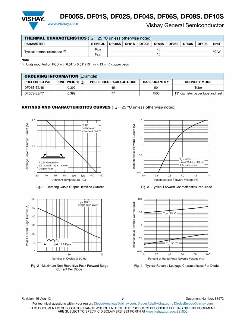
RATINGS AND CHARACTERISTICS CURVES (TA = 25 °C unless otherwise noted)
Fig. 1 - Derating Curve Output Rectified Current
Fig. 2 - Maximum Non-Repetitive Peak Forward SurgeCurrent Per Diode
Fig. 3 - Typical Forward Characteristics Per Diode
Fig. 4 - Typical Reverse Leakage Characteristics Per Diode
THERMAL CHARACTERISTICS (TA = 25 °C unless otherwise noted)PARAMETER SYMBOL DF005S DF01S DF02S DF04S DF06S DF08S DF10S UNIT
Typical thermal resistance (1)RJA 40
°C/W RJL 15
ORDERING INFORMATION (Example)PREFERRED P/N UNIT WEIGHT (g) PREFERRED PACKAGE CODE BASE QUANTITY DELIVERY MODE
DF06S-E3/45 0.399 45 50 Tube
DF06S-E3/77 0.399 77 1500 13" diameter paper tape and reel
20 40 60 80 100 120 140 1600
0.5
1.0
Ambient Temperature (°C)
Ave
rage
For
war
d O
utpu
t Cur
rent
(A
)
60 HzResistive orInductive Load
P.C.B. Mounted on0.51 x 0.51" (13 x 13 mm)Copper Pads
1 10 1000
10
20
30
40
50
60
Number of Cycles at 60 Hz
Pea
k F
orw
ard
Sur
ge C
urre
nt (
A)
TJ = 150 °CSingle Sine-Wave
1.0 Cycle
0.4 0.6 0.8 1.0 1.2 1.40.01
0.1
1
10
Instantaneous Forward Voltage (V)
Inst
anta
neou
s F
orw
ard
Cur
rent
(A
)
TJ = 25 °CPulse Width = 300 µs1 % Duty Cycle
0 20 40 60 80 1000.01
0.1
1
10
100
TJ = 125 °C
TJ = 50 °C
Percent of Rated Peak Reverse Voltage (%)
Inst
anta
neou
s R
ever
se C
urre
nt (
µA)
DF005S, DF01S, DF02S, DF04S, DF06S, DF08S, DF10Swww.vishay.com Vishay General Semiconductor
Revision: 19-Aug-13 3 Document Number: 88573
For technical questions within your region: [email protected], [email protected], [email protected] DOCUMENT IS SUBJECT TO CHANGE WITHOUT NOTICE. THE PRODUCTS DESCRIBED HEREIN AND THIS DOCUMENT
ARE SUBJECT TO SPECIFIC DISCLAIMERS, SET FORTH AT www.vishay.com/doc?91000
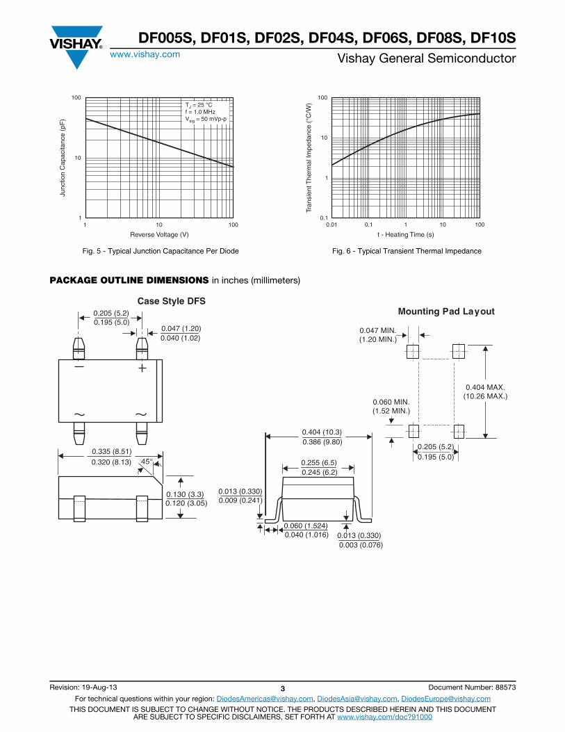
Fig. 5 - Typical Junction Capacitance Per Diode Fig. 6 - Typical Transient Thermal Impedance
PACKAGE OUTLINE DIMENSIONS in inches (millimeters)
1 10 1001
10
100
Reverse Voltage (V)
Junc
tion
Cap
acita
nce
(pF
)
TJ = 25 °Cf = 1.0 MHzVsig = 50 mVp-p
0.01 0.1 1 10 1000.1
1
10
100
t - Heating Time (s)
Tran
sien
t The
rmal
Impe
danc
e (°
C/W
)Mounting Pad Layout
0.255 (6.5)0.245 (6.2)
0.013 (0.330)0.009 (0.241)
0.060 (1.524)0.040 (1.016)
0.404 (10.3)
0.013 (0.330)0.003 (0.076)
0.047 (1.20)0.040 (1.02)
0.205 (5.2)0.195 (5.0)
0.335 (8.51)
0.320 (8.13)
0.130 (3.3)0.120 (3.05)
45°
0.386 (9.80)
Case Style DFS
0.404 MAX.(10.26 MAX.)
0.205 (5.2)0.195 (5.0)
0.047 MIN.(1.20 MIN.)
0.060 MIN.(1.52 MIN.)
Legal Disclaimer Noticewww.vishay.com Vishay
Revision: 08-Feb-17 1 Document Number: 91000
DisclaimerALL PRODUCT, PRODUCT SPECIFICATIONS AND DATA ARE SUBJECT TO CHANGE WITHOUT NOTICE TO IMPROVE RELIABILITY, FUNCTION OR DESIGN OR OTHERWISE.
Vishay Intertechnology, Inc., its affiliates, agents, and employees, and all persons acting on its or their behalf (collectively, “Vishay”), disclaim any and all liability for any errors, inaccuracies or incompleteness contained in any datasheet or in any other disclosure relating to any product.
Vishay makes no warranty, representation or guarantee regarding the suitability of the products for any particular purpose or the continuing production of any product. To the maximum extent permitted by applicable law, Vishay disclaims (i) any and all liability arising out of the application or use of any product, (ii) any and all liability, including without limitation special, consequential or incidental damages, and (iii) any and all implied warranties, including warranties of fitness for particular purpose, non-infringement and merchantability.
Statements regarding the suitability of products for certain types of applications are based on Vishay’s knowledge of typical requirements that are often placed on Vishay products in generic applications. Such statements are not binding statements about the suitability of products for a particular application. It is the customer’s responsibility to validate that a particular product with the properties described in the product specification is suitable for use in a particular application. Parameters provided in datasheets and / or specifications may vary in different applications and performance may vary over time. All operating parameters, including typical parameters, must be validated for each customer application by the customer’s technical experts. Product specifications do not expand or otherwise modify Vishay’s terms and conditions of purchase, including but not limited to the warranty expressed therein.
Except as expressly indicated in writing, Vishay products are not designed for use in medical, life-saving, or life-sustaining applications or for any other application in which the failure of the Vishay product could result in personal injury or death. Customers using or selling Vishay products not expressly indicated for use in such applications do so at their own risk. Please contact authorized Vishay personnel to obtain written terms and conditions regarding products designed for such applications.
No license, express or implied, by estoppel or otherwise, to any intellectual property rights is granted by this document or by any conduct of Vishay. Product names and markings noted herein may be trademarks of their respective owners.
© 2017 VISHAY INTERTECHNOLOGY, INC. ALL RIGHTS RESERVED