Embed Size (px)
Citation preview

Migrating to Achronix FPGA Technology (AN023)
November 19, 2020 www.achronix.com 1
IntroductionMany users transitioning to Achronix FPGA technology will be familiar with existing FPGA solutions from other vendors. Although Achronix technology and tools are very similar to existing FPGA technology and tools, there are some differences. Understanding these differences are needed to achieve the very best performance and quality of results (QoR).
This application note discusses any differences in the Achronix tool flow, highlighting key files and methodologies that users may not be familiar with. Further this application note details the primitive components present in the Achronix fabric, and how they may differ from, or in many cases are similar to, other vendors.
Finally this application note reviews the unique features, particularly focused on AI and ML workloads that are present in the Achronix FPGA devices.
Related DocumentsThis application note is intended to give an overview of any changes that a user may encounter when migrating to Achronix technology. For full details of any of the items described below, the user is directed to the appropriate user guide or application note. Instead of duplicating information, this application note highlights the changes, and refers the user to the appropriate user guide where they can obtain the full information.
A number of user guides are commonly referred to throughout this document
Speedster7t IP Component Library User Guide (UG086) .This user guide describes all the silicon elements on the Speedster7t family. It includes descriptions, and instantiation templates, of the memories, DSP, MLP, NAP and logic primitives.
Synthesis User Guide (UG071). This user guide describes the use of Synplify Pro for synthesis and how to correctly infer memories and DSP. In addition it details synthesis constraints and attributes
(UG070)ACE User Guide . This user guide details all the features and usage of the ACE design environment. It details how to create and run projects, and to analyze and apply advanced techniques for timing closure.
Device MigrationThe Achronix Speedster®7t family has a number of devices available which are comparable to devices from Xilinx and Intel. The following table can be used to select the appropriate alternative device.
Migrating to Achronix FPGA Technology (AN023)November 19, 2020 Application Note

Migrating to Achronix FPGA Technology (AN023)
November 19, 2020 www.achronix.com 2
Note
The suggested device equivalents below are based on comparable resources for LUTs and DFFs. No two manufacturers parts have exactly the same quantity of components, and in addition, the quantity of larger silicon elements such as memories and DSP blocks may vary significantly. The user should satisfy themselves that any device they select has sufficient resources to support their design goals.
Table 1: Equivalent Device Families
Current Vendor Current family Current device Achronix Equivalent
Xilinx
Kintex UltrascaleKU025 - KU060 ac7t750
KU085 to KU115 ac7t1500
Kintex Ultrascale+KU3P to KU13P ac7t750
KU15P to KU19P ac7t1500
Virtex Ultrascale
VU065 ac7t750
VU080 to VU125 ac7t1500
VU160 to VU190 ac7t3000
Virtex Ultrascale+
VU3P ac7t750
VU5P to VU7P ac7t1500
VU9P to VU11P ac7t3000
Intel
Arria 10
GX160 to GX480 ac7t750
GX570 to GX900 ac7t1500
GX900 to GX1150 ac7t3000
GT900 to GT1150 ac7t3000
Stratix 10
GX400 to GX650 ac7t750
GX850 to GX1100 ac7t1500
GX1650 to GX2500 ac7t3000
In addition for designs that are targeting artificial intelligence or machine learning (AI/ML) markets, the Speedster7t family is particularly well suited with its unique blend of machine learning processor (MLP) and network on chip (NoC). Finally, if the user is targeting an ASIC solution as the final goal of the design, the Achronix eFPGA Speedcore family enables FPGA flexibility within a system on chip (SoC).

Migrating to Achronix FPGA Technology (AN023)
November 19, 2020 www.achronix.com 3
Silicon Elements
Programmable FabricAchronix FPGAs have a familiar array of core silicon components making up the programmable fabric.
Table 2: Programmable Fabric Logic Elements
Vendor Lookup Table
Logic Array
Distributed Math Block Memory Logic
Memory DSP PLLs
Primitive Cascade Paths Primitive Cascade
Paths
Achronix LUT6 RLB6 ALU8 BRAM72K Yes LRAM2K DSP64 Yes 16
Intel LUT6 ALM Adder8 M20K No MLAB DSP Yes
Up to 32 fPLLs and 16 I/O PLLs
Xilinx LUT6 CLB CARRY8 RAMB36E2 Yes LUTRAM DSP48E Yes
4-40 CMTs. Each has 1x MMCM and 2x PLL
Many of the core components support similar features, and since the Achronix tool flow uses synthesis from Synopsys, many designs can be directly ported to the Achronix fabric with little or no RTL modifications
Interface SubsystemsA standout feature of the Achronix Speedster7t family is the inclusion of hard interface subsystems located within the I/O ring. These subsystems remove the need for the user to have to implement soft-IP versions of the same cores, with the accompanying effort to implement, possibly integrate with high-speed SerDes, and close timing. In addition, having to use of soft-IP cores consumes valuable FPGA fabric, thereby reducing the effective usable size of the FPGA.
A comparison of the hard interface subsystems across multiple vendors shows the widespread support that Achronix has.

Migrating to Achronix FPGA Technology (AN023)
November 19, 2020 www.achronix.com 4
1.
2.
Table 3: Interface Subsystems
Feature Achronix Intel Xilinx
Speedster7t Arria 10 Stratix 10 Ultrascale Ultrascale+
PCIe Gen5 ×16 Gen3 ×8 Gen3 ×16 Gen3 ×8 Gen3 ×16 / Gen4 ×8
Ethernet Up to 4 × 400G 100G (soft core) 100G Up to 9× 100G Up to 12× 100G
GDDR6 Up to 8 memories, 512 Gbps each memory No No No No
DDR4 72-bits at 3.2G bps/pin DDR4 2400
DDR4 2400
DDR4 2400 (LogiCORE soft IP)
DDR4 2666 (LogiCORE soft IP)
Serdes Up to 112 Gbps Up to 25 Gbps
Upto 58 Gbps Up to 30 Gbps Up to 32 Gbps
HBM No Yes Yes No Yes
NoC Yes No No No No
Note
Entries marked in grey are implemented in soft core logic; there is no equivalent hard IP available in the device.For both PCIe and the SerDes, Achronix supports the very latest available standards/data rates, which exceed what is currently available from other vendors.
Tool MigrationThe Achronix tool flow is composed of two tools; Synplify Pro from Synopsys for synthesis and ACE for place and route. This arrangement differs from other vendors who combine the synthesis stage within their tools. Achronix have chosen Synopsys as their partner for synthesis as they are the recognized market leaders in this field. Synplify Pro is widely used throughout the FPGA industry for synthesis, often being used in preference to the built-in synthesis flow available in other FPGA tool chains.
Both tools have their own user guides which the user is recommended to refer to for a full understanding of the capability of each tool. These are the and (UG071). (UG070)ACE User Guide Synthesis User Guide
The two tools are tightly integrated, with a well established transfer of information between the tools as shown below.

Migrating to Achronix FPGA Technology (AN023)
November 19, 2020 www.achronix.com 5
Figure 1: Synplify Pro and ACE Tool Flow
Feature ComparisonThe combined Achronix tool flow supports all the features that a user would expect from a fully-fledged, mature, CAD environment.
Table 4: Tool Flow Feature Comparison between FPGA Vendors
Feature Achronix Intel Xilinx
Verilog, SystemVerilog and VHDL synthesis (†) Yes Yes Yes
Memory and DSP inferencing(†) Yes Yes Yes
Pre-synthesis RTL technology browser (†) Yes Yes No
Synthesis-only constraints and directives (†) Yes Yes Yes
Post-synthesis schematic viewer (†) Yes Yes Yes
GUI-based project creation Yes Yes Yes
IP configuration wizards Yes Yes Yes
I/O pin layout wizard Yes Yes Yes
Timing driven place and route Yes Yes Yes
Migrating to Achronix FPGA Technology (AN023)
November 19, 2020 www.achronix.com 6
Feature Achronix Intel Xilinx
SDC timing constraints Yes Yes Yes
Placement constraints (elements and regions) Yes Yes Yes
Virtual pins Yes Yes Yes
Floorplanner Yes Yes Yes
Post-route netlist hierarchy browser Yes Yes Yes
Post-route schematic browser No Yes Yes
Graphical display of critical timing paths Yes Yes Yes
Multiple bitstream formats Yes Yes Yes
Bitstream programming and download Yes Yes Yes
On-chip logic analyzer and debugger Yes Yes Yes
All functions available through Tcl script flow Yes Yes Yes
Note
† Supported by Synopsys Synplify Pro for Achronix
Code ChangesAs previously highlighted the Achronix FPGA architecture has a great deal of commonality with alternative vendor architectures, sharing many similar silicon primitives. In addition as Achronix has partnered with Synopsys to provide front-end synthesis capabilities to the Achronix tool flow, few if any RTL changes should be needed when transitioning from other vendors.
For the regular RLB feature set such as LUTs and DFFs, if these are inferred, as would normally be the case, then no changes should be necessary. In addition with normal inferencing, Synplify Pro is able to take advantage of the dedicated ALU within the RLB structure, generating efficient math and counter operations.
If memories and DSPs have been inferred using regular inference templates, Synplify Pro will be able to infer and generate the appropriate memory or MLP part. RTL changes should only be necessary when a design has directly instantiated memory or DSP parts, or where parts with particular data or address widths are required.
The table below details the different macro names and key features of the larger silicon primitives such as block memory, DSP and shift registers. For designs that directly instantiate these parts, it is necessary to either instantiate the Achronix equivalent (examples are given later in this document), or alternatively replace the direct instantiation with an inference template (which aides in code portability).

Migrating to Achronix FPGA Technology (AN023)
November 19, 2020 www.achronix.com 7
Table 5: Equivalent Silicon Macros
Primitive Feature Achronix Intel Xilinx
Block Memory
Name BRAM72K M20K BRAM36
Organization (widest data bus) 144 × 512 40 × 512 72 × 512
Max address wdth (bits) 14 14 15
Max data width (bits) 144 40 36
Byte write enables Yes Yes Yes
Cascade paths to build larger memory arrays Yes No Yes
SDP Yes Yes Yes
TDP No Yes Yes
DSP
Name DSP64 DSP DSP48E
A input (bits) 18 27 27
B input (bits) 27 27 27
Register file set Yes Yes No
Other inputs No No C & D
Input and output cascade paths Yes Yes Yes
Result (bits) 64 64 48
Shift Register
Name LRAM4K – SRL16
Width 72 – 1
Depth 32 – 16
For lower-level silicon primitives, such as I/O ports and global buffers, Xilinx, in particular, requires the use of dedicated components. These components are effectively wrappers around the respective primitives, setting the appropriate constraints. For designs that make use of these wrappers, it is necessary to convert the RTL. In general the Achronix flow does not require proprietary wrappers, instead it uses general RTL to define wires or signals for the appropriate I/O or buffer, and then specifies the operation of that I/O or buffer by using constraints specified in the I/O Designer tool flow. This approach is more aligned to that done for Intel FPGAs.

Migrating to Achronix FPGA Technology (AN023)
November 19, 2020 www.achronix.com 8
1.
2.
Table 6: Equivalent Silicon Primitives
Function Achronix Part Intel Equivalent Xilinx
Single inputWire/signal in RTL Wire/signal in RTL
IBUG
Single output OBUF
Global clock network Wire/signal in RTL, assign to clock network
Wire/signal in RTL assignment to global signal BUFG
Input global buffer per I/O standard
Wire/signal in RTL, I/O assignment, assign to clock network
wire/signal, I/O assignment, global signal assignment
IBUFG_<io standard>
Input per I/O standard Wire/signal and I/O assignment
Wire/signal and I/O assignment
IBUF_<io standard>
Bidirectional I/O per I/O standard
Wire/signal and I/O assignment (1)
IOBUF_<io standard>
Output from global buffer per I/O standard Wire/signal and I/O
assignment
OBUFG_<io standard>
Output per I/O standard
OBUF_<io standard>
Differential I/O bufferWire/signal and I/O assignment (2)
Wire/signal and I/O assignment, _n signal created.
IBUFDS/OBUFDS
16-bit shift register LRAM2K / LRAM4K AUTO_SHIFT_REGISTER_RECOGNITION SRL16
Note
Within ACE, I/O assignment is done using the I/O Designer tool flow. This tool sets all I/O standards, pin locations and directions.
For bidirectional pins, the input, output and output enables wires are presented to the user logic.For differential pins, only the single input or output wire is presented to the user logic.
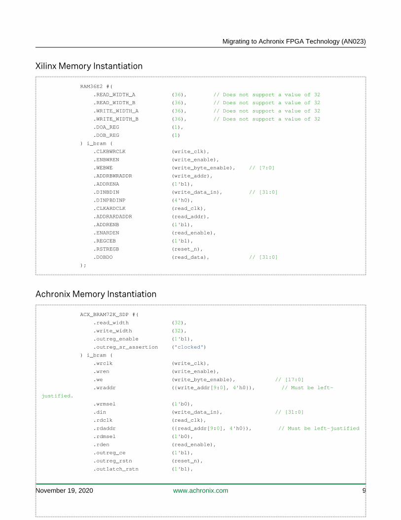
MemoryEmbedded memories in all architectures can be both inferred and instantiated. For inferencing, Synplify Pro supports the usual memory template constructs that the user will be familiar with. If the user has directly instantiated their memory, then as the port functions are very similar, it is an simple task to convert from one vendor instantiation to another. An example is given below of an instantiation of a Xilinx memory, configured as 32 × 1024 SDP with output register, and then of the same configuration done with an Achronix memory
Migrating to Achronix FPGA Technology (AN023)
November 19, 2020 www.achronix.com 9
Xilinx Memory Instantiation
RAM36E2 #(
.READ_WIDTH_A (36), // Does not support a value of 32
.READ_WIDTH_B (36), // Does not support a value of 32
.WRITE_WIDTH_A (36), // Does not support a value of 32
.WRITE_WIDTH_B (36), // Does not support a value of 32
.DOA_REG (1),
.DOB_REG (1)
) i_bram (
.CLKBWRCLK (write_clk),
.ENBWREN (write_enable),
.WEBWE (write_byte_enable), // [7:0]
.ADDRBWRADDR (write_addr),
.ADDRENA (1'b1),
.DINBDIN (write_data_in), // [31:0]
.DINPBDINP (4'h0),
.CLKARDCLK (read_clk),
.ADDRARDADDR (read_addr),
.ADDRENB (1'b1),
.ENARDEN (read_enable),
.REGCEB (1'b1),
.RSTREGB (reset_n),
.DOBDO (read_data), // [31:0]
);
Achronix Memory Instantiation
ACX_BRAM72K_SDP #(
.read_width (32),
.write_width (32),
.outreg_enable (1'b1),
.outreg_sr_assertion ("clocked")
) i_bram (
.wrclk (write_clk),
.wren (write_enable),
.we (write_byte_enable), // [17:0]
.wraddr ({write_addr[9:0], 4'h0}), // Must be left-
justified.
.wrmsel (1'b0),
.din (write_data_in), // [31:0]
.rdclk (read_clk),
.rdaddr ({read_addr[9:0], 4'h0}), // Must be left-justified
.rdmsel (1'b0),
.rden (read_enable),
.outreg_ce (1'b1),
.outreg_rstn (reset_n),
.outlatch_rstn (1'b1),

Migrating to Achronix FPGA Technology (AN023)
November 19, 2020 www.achronix.com 10
.dout (read_data), // [31:0]
.sbit_error (),
.dbit_error ()
);
DSPSimilar to memories, DSP blocks can either be inferred or instantiated. For inference Synplify Pro recognizes many of the commonly used constructs and will infer the appropriate arithmetic block. Alternatively if DSP blocks have been directly instantiated, then it is possible to migrate the instantiation to an Achronix equivalent. The equivalent instantiations for a 27 × 18 multiplier, with one stage of pipelining are shown below
Note
For the purposes of clarity, parameters that are left at their default values, and unused outputs have been removed from the examples below
Xilinx DSP Instantiation
// Default parameters ignored in instantiation
DSP48E2 #(
.A_INPUT ("DIRECT"), // A input from A port
.B_INPUT ("DIRECT"), // B input from B port
.P_REG (1) // One output register
) i_dsp (
.CLK (i_clk),
.ALUMODE (4'h0), // Basic multiplication
.CARRYINSEL (3'b000), // No carry
.INMODE (5'b00000), // Use A/B inputs to multiplier
.OPMODE (9'b0), // Do not use W, X, Y or Z
multipliers
.A ({{2{ain[26]}}, a_in}), // Sign extend 27-bit input
.ACIN (30'h0), // Not used
.B (b_in), // [17:0]
.BCIN (18'h0), // Not used
.C (48'h0), // Not used
.D (27'h0), // Not used
.CARRYIN (1'b0), // No carry
.CARRYCASCIN (1'b0), // Not used
.PCIN (48'h0), // Not used
.RSTA (1'b0), // No input register
.RSTB (1'b0), // No output register
.RSTC (1'b0), // No input register
.RSTD (1'b0), // No output register
.RSTP (i_reset), // Reset output register
.P (dsp_dout[47:0]) // Output vector
);

Migrating to Achronix FPGA Technology (AN023)
November 19, 2020 www.achronix.com 11
Achronix DSP Instantiation
// Default parameters ignored in instantiation
DSP64 #(
.dout_del (1'b1), // Add register to DSP output
.sel_addsub_a (2'b00), // Mult output, sign extended
.sel_addsub_b (1'b0), // 1'b0 = registered dout
.sel_mult_a (2'b00), // 2'b00 = select A input
.sel_mult_b (2'b00), // 2'b00 = select B input
.sel_48_dout (1'b1), // Select 48-bit output
) i_dsp (
.clk (i_clk),
.a (a_in), // [26:0]
.b (b_in), // [17:0]
.sub (1'b0), // Add not subtract
.cin (1'b0), // No carry
.load (1'b0), // No preload
.rnd (1'b0), // No rounding
.mshift (1'b0), // No bit shift
.reg_addr (3'b000), // Register file not used
.ce_dout (1'b1), // Enable output register
.ce_multout (1'b1), // Enable multiplier output
.rstn_a (1'b0), // No input register
.rstn_b (1'b0), // No output register
.rstn_addsub (1'b0),
.rstn_addsub_a (1'b0),
.rstn_dout (i_reset), // Reset output register
.rstn_cascade (1'b0), // No cascade register
.rstn_multout (1'b1),
.dout (dsp_dout[44:0]),
.cout (),
.over_pos (dsp_dout[47]),
.over_neg (dsp_dout[46]),
.match (dsp_dout[45]), // 48-bit output
.fwdi_casc (64'b0),
.fwdi_dout (64'b0),
.fwdi_cin (1'b0),
.fwdi_match (1'b0),
.revi_casc (64'b0),
.revi_dout (32'b0)
);

Migrating to Achronix FPGA Technology (AN023)
November 19, 2020 www.achronix.com 12
ConstraintsBoth Synplify Pro and ACE support the industry-standard SDC file format for constraints. In addition both tools support standard Tcl interfaces for scripting complex constraint processes. Further, each tool, similar to most other tools, support their own constraint file format where tool-specific constraints can be added.
File StructureAlongside RTL, the other key source files of any project are the constraint files, specifying both timing (for Synthesis and Place and Route), physical constraints (such as I/O standards), and placement constraints (I/O pins or placement regions). Within the Achronix tool flow these constraint functions are separated out into multiple files, each with their own application. This structure is in keeping with all other vendors who recommend, as a minimum, that timing and physical constraints should be in separate files. However, it is recognized that many projects do combine all constraints into a single file. Details below are provided to assist in the conversion of constraints into their appropriate files.
Table 7: Constraint File Types and Applications
Tool Extension Application Intel Equivalent Xilinx Equivalent
Synplify
.sdc Synthesis timing constraints. .sdc.xdc with property USED_IN_SYNTHESIS (*)
.fdc Synthesis physical constraints and attributes
.qsf project file
ACE
.sdc Place-and-route timing constraints .sdf.xdc with property USED_IN_IMPLEMENTATION(†)
.pdc Place-and-route physical constraints and attributes
.qsf project file
Table Note
† For Xilinx files, if no property is specified, then the constraint files is used for both synthesis and implementation.
Warning!
It is not possible to use the same SDC file for both Synplify Pro and ACE as the hierarchical path and separator characters differ between the tools. It is necessary to create two files, one for each tool.
Supported SDC CommandsThe following SDC standard commands are supported by both Synplify Pro and ACE (within their respective .
files).sdc

Migrating to Achronix FPGA Technology (AN023)
November 19, 2020 www.achronix.com 13
Table 8: Supported SDC Commands
all_clocks all_inputs all_outputs create_clock
create_generated_clock get_cells get_clocks get_fanout
get_nets get_pins get_ports set_clock_groups
set_clock_latency set_clock_uncertainty set_data_check set_disable_timing
set_false_path set_input_delay set_input_transition set_load
set_max_delay set_min_delay set_multicycle_path
Non-SDC AttributesNon-timing attributes such as physical placement, I/O specifications or synthesis directive differ between tool chains. The table below details some of the common attributes and directives and their equivalents
Table 9: Non-SDC Attributes and Directives
Function Achronix Intel Xilinx
Synplify(†) ACE(†)
Place I/O pin – set_placement chip_pin PACKAGE_PIN
Force signal to be enable on flop syn_useenables – direct_enable DIRECT_ENABLE
Prevent register duplication syn_replicate – dont_replicate DONT_TOUCH
Prevent register retiming syn_retime – dont_retime DONT_TOUCH
Prevent register merging syn_preserve must_keep dont_merge KEEP/DONT_TOUCH
FSM enumeration encoding syn_encoding – enum_encoding
(VHDL) fsm_encoding
Full case statement full_case – full_case (Verilog) full_case (Verilog)
Prevent synthesis optimization syn_keep must_keep keep KEEP
Maximum fanout syn_maxfan fanout_limit maxfan max_fanout
Multiplier style syn_dspstyle – multstyle mult_style
Prevent logic optimization syn_keep must_keep noprune DONT_TOUCH

Migrating to Achronix FPGA Technology (AN023)
November 19, 2020 www.achronix.com 14
Function Achronix Intel Xilinx
Case statement as parallel case parallel_case – parallel_case parallel_case
Prevent redundant logic optimization syn_preserve must_keep preserve DONT_TOUCH
RAM style syn_ramstyle – ramstyle ram_style
ROM style syn_romstyle – romstyle rom_style
Enumerator encoding syn_enum_encoding – syn_encoding fsm_encoding
Disable/enable synthesis for portions of the code
synthesis_on/off or translate_on/off – translate_on/off translate_on/off
Implement I/O register in I/O block syn_useioff ace_useioff useioff IOB
Specify Verilog version -vlog_std – verilog_input_version HDL file property in project
Specify VHDL version set_option -vhdl<version> – vhdl_input_version HDL file property
in project
Table Note
† Synthesis only directives are executed by Synplify Pro, other non-synthesis directives are executed by ACE. For certain functions it is necessary to apply directives to both tools.
Search Considerations
SDC Versus Tcl FindDepending on the constraint file type, different commands should be used when searching for and assembling collections of objects.
.sdc files – The SDC commands such as , should be used.get_pins get_ports
.fdc /.pdc files – The Tcl command should be used.find
Hierarchical PathsOne area where tools can differ is in the separators and nomenclature used for hierarchical paths. The respective paths to an object are shown below
# Synplify hierarchical path
i_top_level.i_module_instance.gb_generate_loop\[0\].i_generated_instance.pin
# ACE hierarchical path
i_top_level.i_module_instance.gb_generate_loop_0__i_generated_instance/pin
The key differences are:

Migrating to Achronix FPGA Technology (AN023)
November 19, 2020 www.achronix.com 15
The key differences are:
Generated blocks – For a Verilog generate loop, within Synplify Pro this is expressed as . For ACE this is expressed as generate_loop_block_name[index].i_generated_instance
generate_loop generate_loop_block_name_index__i_generated_instance
Note
There is a double underscore after the index.
Pins – For the pin on a module, Synplify uses the same "." separator as used for the hierarchy, for example, ACE uses the "/" separator for pins only, hence .i_my_block.pin i_my_block/pin
Note
When searching for pins, especially when using the SDC command as a search into an get_pinsSDC timing command ( etc.), it is usually necessary to specify the pins of create_generated_clockthe lowest level primitive rather than pins midway down the hierarchy. For example
set_generated_clock -name clk_div2 -divide_by 2 -source [get_ports clk_in] [get_pins
i_top_level.i_my_clock_block/clk_div_2] // Incorrect
set_generated_clock -name clk_div2 -divide_by 2 -source [get_ports clk_in] [get_pins
i_top_level.i_my_clock_block.i_CLKDIV/clk_out] // Correct
Character Escape SequencesIn many tools it is necessary to use the escape character, "\", before reserved characters in an SDC or Tcl command. These sequences can then vary between a direct single-line constraint, creating a variable to be reused in later constraints, and creating a Tcl loop of constraints. The required escape sequences are shown below.
Direct Single-Line ConstraintSynplify Pro – use escape character
[ get_pins i_top_level.i_module_instance.gb_generate_loop\[0\].i_generated_instance.pin\[0\] ]
ACE – no escape character needed
[ get_pins i_top_level.i_module_instance.gb_generate_loop_0__i_generated_instance.pin[0]
Variable Used in Multiple ConstraintsSynplify – need escape character to be present in string. So escape both the escape and reserved characters
set target_pin "i_top_level.i_module_instance.gb_generate_loop\\\[0\\\].i_generated_instance.
pin\\\[0\\\]"

Migrating to Achronix FPGA Technology (AN023)
November 19, 2020 www.achronix.com 16
ACE – escape the reserved character in the string
set target_pin "i_top_level.i_module_instance.gb_generate_loop_0__i_generated_instance\/pin\[0\]"
Tcl Loop to Apply Constraint to Multiple PinsSynplify
for {set index 0} {$index < 4} {incr index} {
create_generated_clock -name my_clk\_\\\$index -source [get_ports clk_in] [get_pins
i_top_level.i_pll.clock_output\\\[$index\\\]]
}
ACE
for {set index 0} {$index < 4} {incr index} {
create_generated_clock -name my_clk\_\\\$index -source [get_ports clk_in] [get_pins
i_top_level.i_pll.clock_output\[$index\]]
}
Synplify FPGA Design Constraints (FDC)The FDC file format is supported by Synplify Pro for any non-timing related constraints. Using FDC the user can select groups of instances and apply specific synthesis constraints to those instances without having to modify the original RTL. The example below shows three common FDC operations.
Example 1Example of how to change the available resources in the target device:
define_global_attribute syn_allowed_resources {blockmults=0}
Example 2Example of how to set a soft compile point using wildcards supports the compile point changing name on each run:
foreach inst [c_list [find -hier -view oc_avr_hp_cm4*]] {
define_compile_point $inst -type {soft}
}

Migrating to Achronix FPGA Technology (AN023)
November 19, 2020 www.achronix.com 17
Example 3Example of ensuring RAMs only inferred for sufficiently large register sets:
define_global_attribute {syn_max_memsize_reg} {2048}
ACE Placement Constraints (PDC)The PDC file format is supported by ACE for any non-timing related constraints. Using PDC the user can place groups of instances, define I/O locations and placement regions, and apply specific clock or I/O parameters The example below shows three common PDC operations.
Example 1Fix a pin location:
set_placement -fixed -batch {p:clk} {d:i_user_06_00_trunk_00[7]}
Example 2Limit the fanout on a net:
set_property fanout_limit 10 [find {*bist_enable_reg1*\[0\]*} -nets] -warning
Achronix EnhancementsIn addition to supporting the regular silicon components that users are accustomed to, the Speedster7t family has two unique features which make it particularly suitable for AI/ML or any other form of accelerator application.
Network on ChipThe network on chip (NoC) is a two-dimensional dedicated network for high-speed data transmission, which is placed above the FPGA fabric. This NoC enables high-speed data transfer from the FPGA fabric to either the dedicated interface subsystems on the device (GDDR6, DDR4, PCIe Gen5 or 400G Ethernet) or to other points on the die. This one features greatly reduces congestion and solves many of the current FPGA data transfer issues, whether that be congestion, timing closure or resource utilization.

Migrating to Achronix FPGA Technology (AN023)
November 19, 2020 www.achronix.com 18
Figure 2: Speedster7t Network on Chip
Access between the NoC and the FPGA fabric is done using network access points (NAPs). These NAPs use the industry-standard AXI4 interface., enabling users to easily reuse any existing IP they may possess to communicate directly to the NoC.
In addition the NoC can be used to send data directly between interface subsystems. For example, the PCIe subsystem can directly populate the GDDR6 or DDR4 memories without consuming any of the FPGA fabric at all, This capability also saves the designer the time and effort of creating and trying to close timing between these high-speed interfaces as they would have to do with current devices. In total the NoC can support a throughput of greater than 20 Tbps.
The NoC is fully described in (UG089), and Achronix further provides a Speedster7t Network on Chip User Guidededicated NoC reference design along with multiple other reference designs that use the NoC to communicate directly with each of the hard interface subsystems within a Speedster7t FPGA.
Machine Learning ProcessorThe machine learning processor (MLP) is a powerful math block optimized for AI/ML math operations. Each MLP can have up to 32 multipliers, ranging from 3-bit integer to 24-bit floating point, supported natively in silicon. The MLP is optimized to support vector and matrix math with integrated memories and register files to allow for easy reuse of coefficients, kernels or intermediate results. The result is that real-world applications running on a Speedster7t device can achieve 8600 images per second using the Resnet-50 algorithm.
Full details of the MLP can be found in the (UG086) and Speedster7t IP Component Library User Guide(UG088). In addition Achronix provides multiple reference Speedster7t Machine Learning Processor User Guide
designs demonstrating functions such as dot product, matrix vector math and 2D convolutions using the MLP.

Migrating to Achronix FPGA Technology (AN023)
November 19, 2020 www.achronix.com 19
ConclusionAs can be seen, there is a clear flow for users to migrate their designs to an Achronix FPGA. These devices support many familiar components, and for designs that require high data throughput, dedicated interface hard IP, or AI/ML math capabilities, these designs will be further boosted by the unique MLP and NoC capabilities. In addition these devices are supported by a mature and comprehensive tool flow that offers the rich feature set users require to develop and debug today's complex FPGAs.
To get started design with Achronix solutions, visit .Getting Started with Achronix
Revision History
Version Date Description
1.0 19 Nov 2020 Initial Achronix release.

Migrating to Achronix FPGA Technology (AN023)
November 19, 2020 www.achronix.com 20
Website: www.achronix.comE-mail : [email protected]
2903 Bunker Hill LaneSanta Clara, CA 95054USA
Achronix Semiconductor Corporation
Copyright © 2020 Achronix Semiconductor Corporation. All rights reserved. Achronix, Speedcore, Speedster, and ACE are trademarks of Achronix Semiconductor Corporation in the U.S. and/or other countries All other trademarks are the property of their respective owners. All specifications subject to change without notice.
Notice of DisclaimerThe information given in this document is believed to be accurate and reliable. However, Achronix Semiconductor Corporation does not give any representations or warranties as to the completeness or accuracy of such information and shall have no liability for the use of the information contained herein. Achronix Semiconductor Corporation reserves the right to make changes to this document and the information contained herein at any time and without notice. All Achronix trademarks, registered trademarks, disclaimers and patents are listed at http://www.achronix.com/legal.