Embed Size (px)
Citation preview
Freescale SemiconductorApplication Note
© Freescale Semiconductor, Inc., 2004, 2007. All rights reserved.
This application note outlines relevant considerations for migrating from the MPC826x (PowerQUICC™ II) family of devices to the higher performance MPC85xx (PowerQUICC III) family. This document explains the differences between the main system blocks and internal cores, explores the initialization and reset sequences, and details the minor modifications required to run existing PowerQUICC II software on PowerQUICC III.
A basic understanding of the system blocks and operation of the PowerQUICC II microprocessor family and HiP7 derivatives is assumed. It is important you be familiar with the following technical references to understand the correct terminology and general MPC85xx and e500 programming model. Refer to the MPC8560 PowerQUICC™ III Integrated Communications Processor Reference Manual.
The following Freescale documents are referenced throughout this application note:
• MPC8560 PowerQUICC™ III Integrated Communications Processor Reference Manual (MPC8560RM)
• PowerPC™ e500 Core Complex Reference Manual (E500CORERM)
• MPC603e and e500 Register Model Comparison (AN2490)
Contents1 System Overview. . . . . . . . . . . . . . . . . . . . . . . . . . . . . 22 Core Differences . . . . . . . . . . . . . . . . . . . . . . . . . . . . . 33 Communications Processor Module (CPM) . . . . . . . 114 New Features on PowerQUICC III . . . . . . . . . . . . . . 145 Initialization, Reset and Boot Procedures . . . . . . . . . 286 Software Considerations . . . . . . . . . . . . . . . . . . . . . . 307 Summary . . . . . . . . . . . . . . . . . . . . . . . . . . . . . . . . . . 33
Migrating from PowerQUICC™ II to PowerQUICC IIIby Nigel Dick
NCSD ApplicationsFreescale Semiconductor, Inc.East Kilbrade, Scotland
Document Number: AN2662Rev. 2, 01/2007
Migrating from PowerQUICC™ II to PowerQUICC III, Rev. 2
2 Freescale Semiconductor
System Overview
The products described in this document are PowerPC™ microprocessor cores. This application note outlines differences between the register models defined by the Apple/IBM/Freescale (AIM) and Book E versions of the PowerPC architecture and the registers implemented in the MPC603e processor and the e500 microprocessor core.
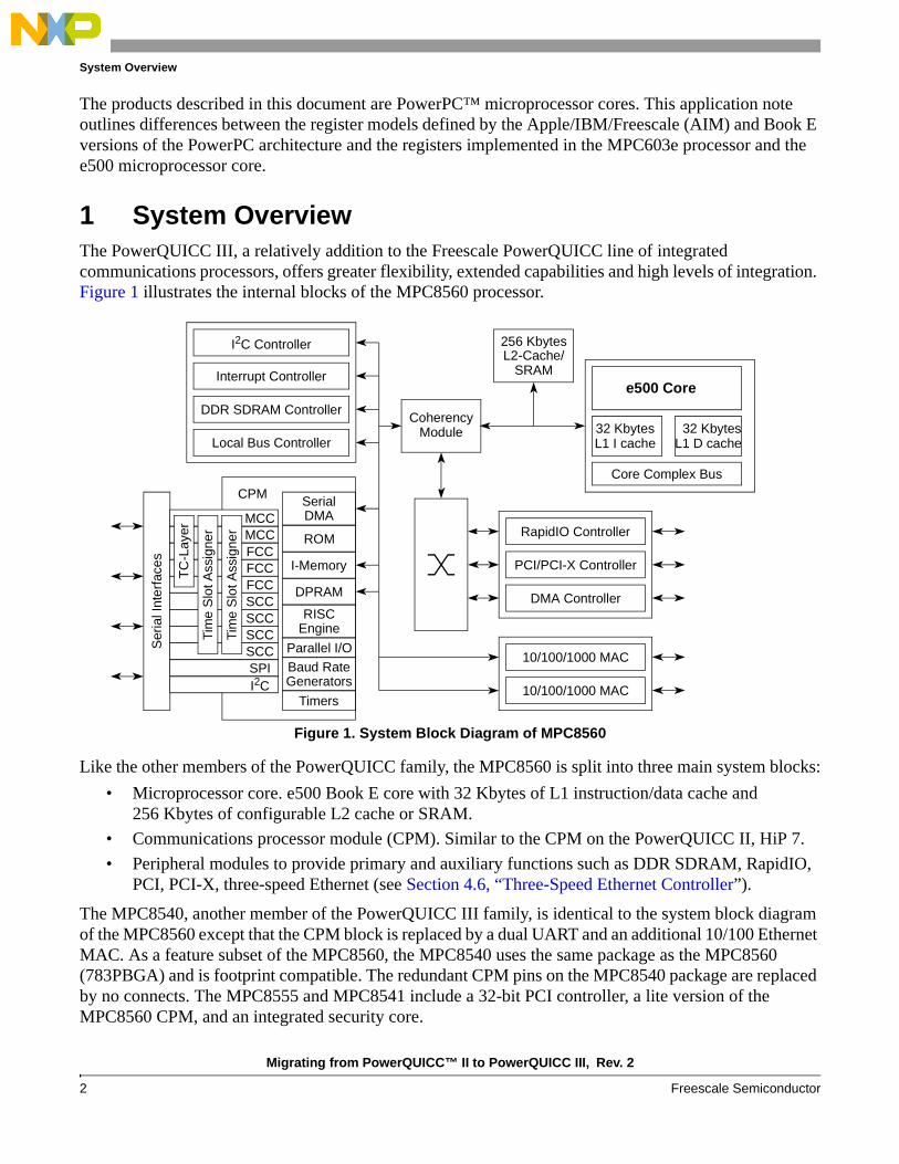
1 System OverviewThe PowerQUICC III, a relatively addition to the Freescale PowerQUICC line of integrated communications processors, offers greater flexibility, extended capabilities and high levels of integration. Figure 1 illustrates the internal blocks of the MPC8560 processor.
Figure 1. System Block Diagram of MPC8560
Like the other members of the PowerQUICC family, the MPC8560 is split into three main system blocks:
• Microprocessor core. e500 Book E core with 32 Kbytes of L1 instruction/data cache and 256 Kbytes of configurable L2 cache or SRAM.
• Communications processor module (CPM). Similar to the CPM on the PowerQUICC II, HiP 7.
• Peripheral modules to provide primary and auxiliary functions such as DDR SDRAM, RapidIO, PCI, PCI-X, three-speed Ethernet (see Section 4.6, “Three-Speed Ethernet Controller”).
The MPC8540, another member of the PowerQUICC III family, is identical to the system block diagram of the MPC8560 except that the CPM block is replaced by a dual UART and an additional 10/100 Ethernet MAC. As a feature subset of the MPC8560, the MPC8540 uses the same package as the MPC8560 (783PBGA) and is footprint compatible. The redundant CPM pins on the MPC8540 package are replaced by no connects. The MPC8555 and MPC8541 include a 32-bit PCI controller, a lite version of the MPC8560 CPM, and an integrated security core.
SerialDMA
CPM
Ser
ial I
nter
face
s
MCCMCCFCCFCCFCCSCCSCCSCCSCCSPII2C
Tim
e S
lot A
ssig
ner
Tim
e S
lot A
ssig
ner
TC
-Lay
er
ROM
I-Memory
DPRAM
RISCEngine
Parallel I/OBaud RateGenerators
Timers
RapidIO Controller
DDR SDRAM ControllerCoherency
Module 32 Kbytes 32 Kbytes
Core Complex Bus
e500 Core
256 KbytesL2-Cache/
SRAM
I2C Controller
PCI/PCI-X Controller
DMA Controller
10/100/1000 MAC
10/100/1000 MAC
Interrupt Controller
Local Bus Controller L1 I cache L1 D cache
Migrating from PowerQUICC™ II to PowerQUICC III, Rev. 2
Freescale Semiconductor 3
Core Differences
2 Core DifferencesThis section summarizes the Book E architecture and its compatibility with the original version of the PowerPC architecture as it was defined by Apple, IBM, and Freescale and implemented in the 603e core (referred to as the AIM version of the PowerPC architecture). The e500 core is the Freescale 32-bit implementation of the Book E architecture.The MPC8540 and MPC8560 devices implement the e500 core. This section describes the differences between the e500 core and the 603e core used in PowerQUICC II devices.
The e500 processor core is a low-power implementation of the family of reduced instruction set computing (RISC) embedded processors. The e500 implements the 32-bit portion of the Book E architecture using the lower words in the 64-bit general-purpose registers (GPRs). Book E allows processors to provide auxiliary processing units (APUs), which are extensions to the architecture. The most significant of these on the e500 is the signal processing engine APU (SPE APU), which includes a suite of vector instructions that use the upper and lower halves of the GPRs as a single two-element operand. Most APUs implemented on the e500 are defined by the Freescale Book E implementation standards (EIS).
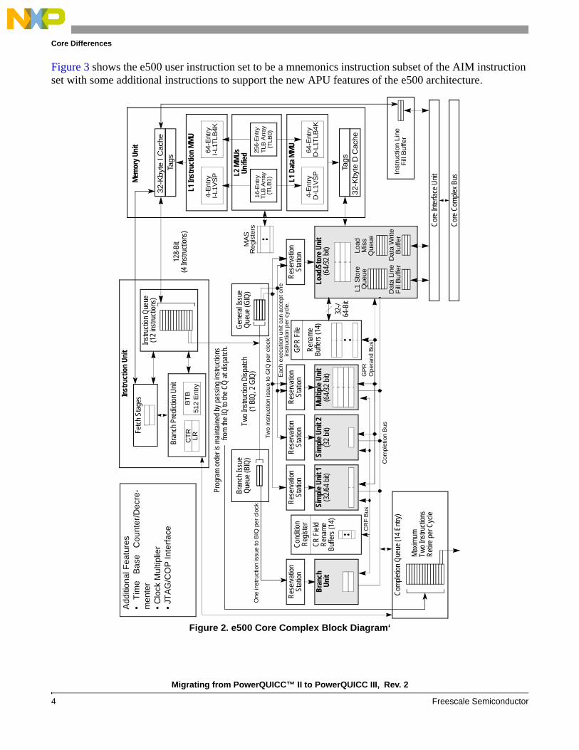
Like the 603e, the e500 provides 32-bit effective addresses, integer data types of 8, 16, and 32 bits, and a 32-bit floating-point data type. The SPE APU on the e500 also supports signed and unsigned fractional data types of 32 bits. The core complex is a superscalar processor that can issue two instructions and complete two instructions per clock cycle. A block diagram of the core complex is shown in Figure 2.
2.1 Instruction Set DifferencesIn user-mode the e500 core executes legacy user-mode binaries and object files with the following exceptions:
• The e500 core uses GPRs for floating point operations instead of separate floating point registers (FPRs) used in the AIM architecture. The floating point instructions on the e500 only support single precision operations and have different encoding from those on AIM processors. These changes are generally handled by recompiling the source code with an e500 compiler.
• The e500 architecture is a 32-bit implementation and 64-bit operation instructions are not supported. Any 64-bit instructions force an illegal instruction exception.
• External control input/output word index (eciwx and ecowx) instructions are not supported.
• No string instructions are implemented in the e500 architecture. To support legacy binaries, it is necessary to add some trap emulation code for the missing instructions.
The supervisor mode instruction set defined by the AIM version of the PowerPC architecture is compatible with the e500 with the following exceptions:
• The MMU architecture is different, and some TLB manipulation instructions have different semantics—tlbsync, tlbivax, tlbre, tlbwe.
• Instructions that support BATs and segment registers are not implemented due to the difference in the MMU architecture of the e500. See Section 2.5, “Memory Management,” for more information.
• New instructions, such as rfci (Return from Critical Interrupt), bbelr/bblels (Branch Buffer Entry Lock Reset/Branch Buffer Load Entry and Lock Set), wrtee[i] (Write MSR External Enable)
Migrating from PowerQUICC™ II to PowerQUICC III, Rev. 2
4 Freescale Semiconductor
Core Differences
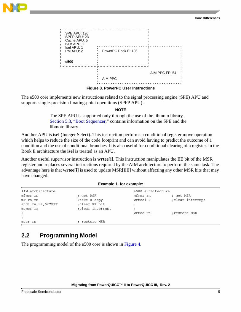
Figure 3 shows the e500 user instruction set to be a mnemonics instruction subset of the AIM instruction set with some additional instructions to support the new APU features of the e500 architecture.
Figure 2. e500 Core Complex Block Diagram‘
Res
erva
tion
Stat
ion
Res
erva
tion
Stat
ion
Res
erva
tion
Stat
ion
Add
ition
al F
eatu
res
• T
ime
Bas
e C
ount
er/D
ecre
-m
ente
r•
Clo
ck M
ultip
lier
• JT
AG
/CO
P In
terf
ace
Fetc
h St
ages
Bran
ch P
redi
ctio
n U
nit
BT
B51
2 E
ntry
CT
RLR
Inst
ruct
ion
Uni
t
Inst
ruct
ion
Que
ue(1
2 in
stru
ctio
ns)
Prog
ram
ord
er is
mai
ntai
ned
by p
assi
ng in
stru
ctio
ns
Res
erva
tion
Bra
nch
Uni
t
GPR
File
Com
plet
ion
Que
ue (1
4 En
try)
Load
/Sto
re U
nit
32-/
64-B
it
L2 M
MUs 25
6-E
ntry
T
LB A
rray
16-E
ntry
Con
ditio
n
CR
Fie
ld
128-
Bit
Gen
eral
Issu
eQ
ueue
(GIQ
)Br
anch
Issu
eQ
ueue
(BIQ
)
(TLB
0)T
LB A
rray
(TLB
1)
Reg
iste
r
Unifi
ed
L1 D
ata
MM
U
64-E
ntry
D
-L1T
LB4K
4-E
ntry
D
-L1V
SP
Two
Inst
ruct
ion
Dis
patc
h(1
BIQ
, 2 G
IQ)
Cor
e In
terfa
ce U
nit
L1 In
stru
ctio
n M
MU
64-E
ntry
I-
L1T
LB4K
4-E
ntry
I-
L1V
SP
32-K
byte
I C
ache
Stat
ion
Res
erva
tion
Stat
ion
Sim
ple
Uni
t 1(3
2/64
bit)
Sim
ple
Uni
t 2(3
2 bi
t)M
ultip
le U
nit
(64/
32 b
it)
(64/
32 b
it)
Mem
ory
Unit
(4 In
stru
ctio
ns)
Tags
Tags
32-K
byte
D C
ache
Max
imum
MA
SR
egis
ters
Two
Inst
ruct
ions
R
etire
per
Cyc
le
from
the
IQ to
the
CQ
at d
ispa
tch.
Load
Dat
a Li
neF
ill B
uffe
rD
ata
Writ
eB
uffe
rIn
stru
ctio
n Li
ne
Ren
ame
Buffe
rs (1
4)
Fill
Buf
fer
Ren
ame
Buffe
rs (1
4)
GP
R
Com
plet
ion
Bus
Ope
rand
Bus
CR
F B
us
Two
inst
ruct
ion
issu
e to
GIQ
per
clo
ck
One
inst
ruct
ion
issu
e to
BIQ
per
clo
ck
L1 S
tore
Que
ueM
iss
Que
ue
Cor
e C
ompl
ex B
us
Eac
h ex
ecut
ion
unit
can
acce
pt o
ne in
stru
ctio
n pe
r cy
cle.
Migrating from PowerQUICC™ II to PowerQUICC III, Rev. 2
Freescale Semiconductor 5
Core Differences
Figure 3. PowerPC User Instructions
The e500 core implements new instructions related to the signal processing engine (SPE) APU and supports single-precision floating-point operations (SPFP APU).
NOTE
The SPE APU is supported only through the use of the libmoto library. Section 5.3, “Boot Sequencer,” contains information on the SPE and the libmoto library.
Another APU is isel (Integer Select). This instruction performs a conditional register move operation which helps to reduce the size of the code footprint and can avoid having to predict the outcome of a condition and the use of conditional branches. It is also useful for conditional clearing of a register. In the Book E architecture the isel is treated as an APU.
Another useful supervisor instruction is wrtee[i]. This instruction manipulates the EE bit of the MSR register and replaces several instructions required by the AIM architecture to perform the same task. The advantage here is that wrtee[i] is used to update MSR[EE] without affecting any other MSR bits that may have changed.
Example 1. for example:
AIM architecture e500 architecturemfmsr rn ; get MSR mfmsr rn ; get MSRmr ra,rn ;take a copy wrteei 0 ;clear interruptandi ra,ra,0x7FFF ;clear EE bit :mtmsr ra ;clear interrupt :: wrtee rn ;restore MSR:mtsr rn ; restore MSR
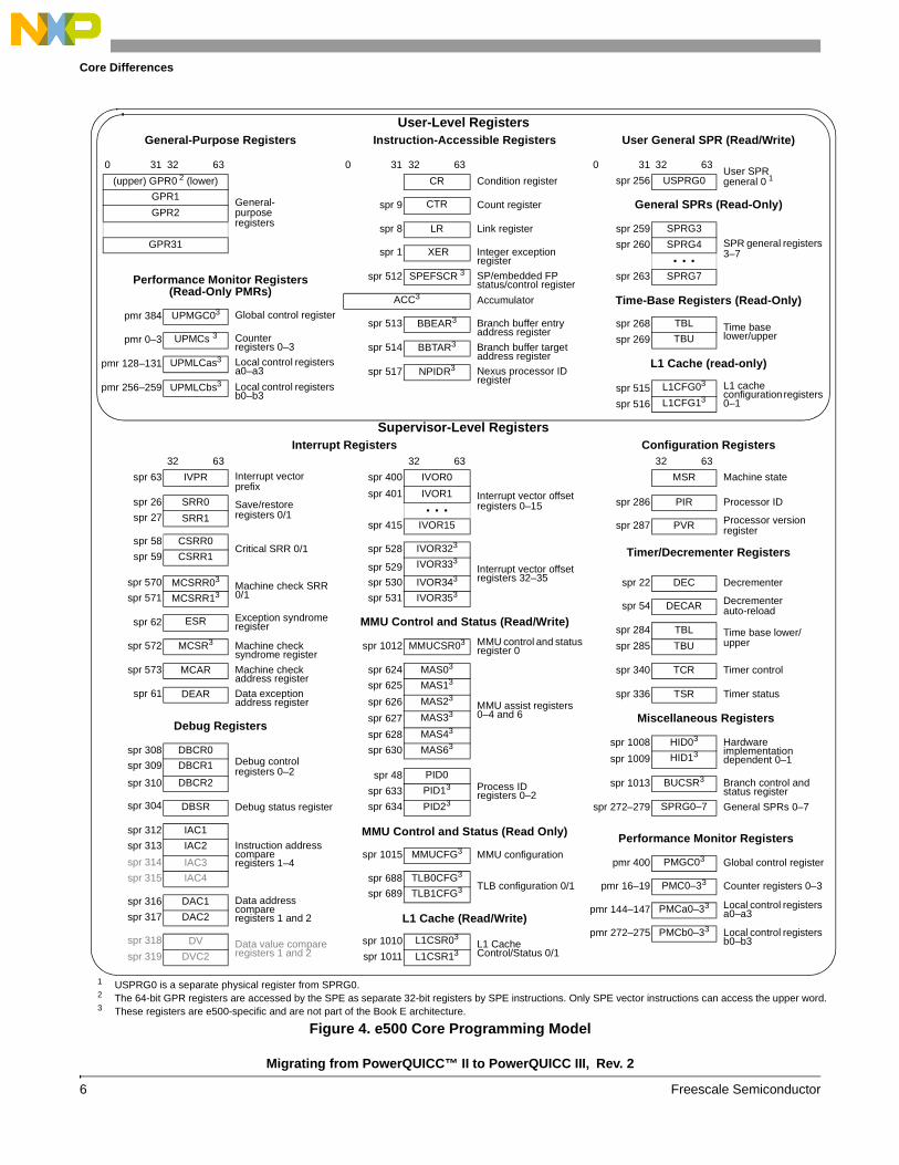
2.2 Programming ModelThe programming model of the e500 core is shown in Figure 4.
SPE APU: 196SPFP APU: 23Cache APU: 5BTB APU: 2Isel APU: 1PM APU: 2 PowerPC Book E: 185
e500
AIM PPC
AIM PPC FP: 54
Migrating from PowerQUICC™ II to PowerQUICC III, Rev. 2
6 Freescale Semiconductor
Core Differences
Figure 4. e500 Core Programming Model
User-Level RegistersGeneral-Purpose Registers Instruction-Accessible Registers User General SPR (Read/Write)
0 31 32 63 0 31 32 63 0 31 32 63User SPR general 0 1
1 USPRG0 is a separate physical register from SPRG0.
(upper) GPR0 2 (lower)
2 The 64-bit GPR registers are accessed by the SPE as separate 32-bit registers by SPE instructions. Only SPE vector instructions can access the upper word.
General-purpose registers
CR Condition register spr 256 USPRG0
GPR1spr 9 CTR Count register General SPRs (Read-Only)
GPR2
spr 8 LR Link register spr 259 SPRG3
SPR general registers 3–7
GPR31 spr 260 SPRG4 spr 1 XER Integer exception
register • • •
Performance Monitor Registers (Read-Only PMRs)
spr 512 SPEFSCR 3
3 These registers are e500-specific and are not part of the Book E architecture.
SP/embedded FP status/control register
spr 263 SPRG7
ACC3 Accumulator Time-Base Registers (Read-Only)Global control registerpmr 384 UPMGC03
spr 513 BBEAR3 Branch buffer entry address register
spr 268 TBL Time base lower/upperpmr 0–3 UPMCs 3 Counter
registers 0–3spr 269 TBU
spr 514 BBTAR3 Branch buffer target address register
pmr 128–131 UPMLCas3 Local control registers a0–a3
L1 Cache (read-only)spr 517 NPIDR3 Nexus processor ID
register L1 cache configuration registers 0–1
pmr 256–259 UPMLCbs3 Local control registers b0–b3
spr 515 L1CFG03
spr 516 L1CFG13
Supervisor-Level RegistersInterrupt Registers Configuration Registers
32 63 32 63 32 63
spr 63 IVPR Interrupt vectorprefix
spr 400 IVOR0
Interrupt vector offset registers 0–15
MSR Machine state
spr 401 IVOR1 spr 26 SRR0 Save/restore
registers 0/1spr 286 PIR Processor ID
• • •spr 27 SRR1 Processor version
registerspr 415 IVOR15 spr 287 PVR
spr 58 CSRR0Critical SRR 0/1 spr 528 IVOR323
Interrupt vector offset registers 32–35
Timer/Decrementer Registersspr 59 CSRR1 spr 529 IVOR333
spr 570 MCSRR03Machine check SRR 0/1
spr 530 IVOR343 spr 22 DEC Decrementer
spr 571 MCSRR13 spr 531 IVOR353Decrementer auto-reload spr 54 DECAR
Exception syndrome register spr 62 ESR MMU Control and Status (Read/Write)
spr 284 TBL Time base lower/ upper MMU control and status
register 0spr 572 MCSR3 Machine check syndrome register
spr 1012 MMUCSR03 spr 285 TBU
spr 573 MCAR Machine check address register
spr 624 MAS03
MMU assist registers 0–4 and 6
spr 340 TCR Timer control
spr 625 MAS13
spr 61 DEAR Data exception address register
spr 336 TSR Timer statusspr 626 MAS23
spr 627 MAS33 Miscellaneous RegistersDebug Registers
spr 628 MAS43
spr 1008 HID03 Hardware implementation dependent 0–1
spr 308 DBCR0Debug control registers 0–2
spr 630 MAS63
spr 1009 HID13
spr 309 DBCR1 spr 48 PID0
Process IDregisters 0–2
spr 310 DBCR2 spr 1013 BUCSR3 Branch control and status registerspr 633 PID13
spr 304 DBSR Debug status register spr 634 PID23 spr 272–279 SPRG0–7 General SPRs 0–7
spr 312 IAC1
Instruction address compareregisters 1–4
MMU Control and Status (Read Only) Performance Monitor Registersspr 313 IAC2
spr 1015 MMUCFG3 MMU configurationspr 314 IAC3 pmr 400 PMGC03 Global control register
spr 315 IAC4 spr 688 TLB0CFG3
TLB configuration 0/1 pmr 16–19 PMC0–33 Counter registers 0–3Data address compare registers 1 and 2
spr 689 TLB1CFG3
spr 316 DAC1 Local control registers a0–a3pmr 144–147 PMCa0–33
spr 317 DAC2 L1 Cache (Read/Write)pmr 272–275 PMCb0–33 Local control registers
b0–b3spr 318 DV Data value compare registers 1 and 2
spr 1010 L1CSR03L1 Cache Control/Status 0/1spr 319 DVC2 spr 1011 L1CSR13
Migrating from PowerQUICC™ II to PowerQUICC III, Rev. 2
Freescale Semiconductor 7
Core Differences
NOTE
Differences between the e500 and the 603e core register sets are described in the MPC603e and e500 Register Model Comparison (AN2490).
Unlike the AIM version of the PowerPC architecture, where little-endian mode is controlled on a system basis, Book E allows control of endian mode on a memory page basis. The e500 core also affects true little-endian mode by byte swapping.
2.3 Internal Memory SubsystemBoth Book E and AIM versions of the PowerPC architecture provide separate instruction and data memory resources. In addition to the internal 32-Kbyte L1 instruction and 32-Kbyte L1 data cache on the e500 core, the PowerQUICC III has 256 Kbytes of L2 cache, which is often referred to as the memory complex. This structure is configurable and its function can be switched between SRAM or cache, or a combination of both SRAM and cache.
Configured as memory-mapped SRAM, the memory complex can either be split into two separate blocks of 128 Kbytes each, or one large 256 Kbyte SRAM block. In full cache mode, all 256 Kbytes of the memory complex are used as L2 cache. Finally, in half-SRAM/half-cache mode, 128 Kbytes of memory-mapped SRAM and 128 Kbytes of cache are created.
The L2 cache is an 8-way, set-associative, write-through, front-side cache that supports locking on either a line-per-line basis or on the complete block, unlike the PowerQUICC II, where only the entire cache could be locked or up to a maximum of three ways. Locking cache blocks allows code in specific areas to be locked so that it is not modified or updated. For example, this feature can be used to store a non-changing, but often used subroutine, which can be stored in cache and then locked to enable optimal code efficiency. Both e500 and 603e cores use the same cache control instructions so that data cache coherency instructions can be used on the PowerQUICC III. The L2 cache on the PowerQUICC III also has hit under miss capability, parity checking and generation and a feature called cache stashing.
Stashing allows external masters that drive transactions into the chip to force certain data into the L2 cache to increase performance. For example, an Ethernet routing application where the processor is simply receiving an IP header, interrogating the recipient address and forwarding the packet back out, without looking at the actual payload. Stashing, for example, allows the Gigabit Ethernet controller on the PowerQUICC III to stash a copy of the header into the L2 cache, so that when the cache gets a hit, it retrieves this information rather than wasting valuable cycles retrieving the information from DDR SDRAM.
2.4 Interrupt HandlingInterrupt handling is generally the same as defined in the AIM version of the PowerPC architecture for the e500, with the following differences:
• Book E processors use the IVPR and IVORs to set exception vectors individually. They can also be set to the address offsets defined in the OEA to provide compatibility with AIM processors. See Section 6.1, “Exception Handling,” for additional information).
• Book E defines a new critical interrupt, that provides an extra level of interrupt nesting. The critical interrupt includes critical and watchdog timer time-out inputs.
Migrating from PowerQUICC™ II to PowerQUICC III, Rev. 2
8 Freescale Semiconductor
Core Differences
• The e500 implements the machine check exception differently from the Book E and from the AIM definition. It defines a Return from Machine Check Interrupt instruction, rfmci, and two machine check save/restore registers, MCSRR0 and MCSRR1.
2.5 Memory ManagementThe e500 core implements a straightforward virtual address space that complies with the Book E MMU definition, eliminating segment registers and block address translation resources. Book E defines resources for fixed 4-Kbyte pages and multiple, variable page sizes that can be configured in a single implementation. TLB management is provided with new instructions and SPRs. The e500 core contains a two-level MMU structure as shown in Figure 5.
Figure 5. e500 Core MMU Structure
The L1 MMU is maintained automatically by the hardware and is transparent to the software. It consists of two four-entry fully associative TLB arrays. One array for instruction and another for data. These arrays support nine page sizes. There are also two 64-entry, 4-way set associative TLB arrays that support fixed (4 Kbyte) page sizes. As a result, the L1 MMU is structured into two similar MMU blocks, one MMU block is used for instruction and the other MMU block is for data.
The L2 MMU is programmed by the user. It consists of one 16-entry, fully associative unified TLB array, TLB1, which supports nine page sizes. This is similar to the BAT registers in the AIM architecture. There is also a 256-entry, two-way set associative unified TLB array called TLB0 which supports fixed page
0Global tablewith page
mapping of all
availablememoryTLB04K
255
0
TLB115
(Variable)
0
MAS 0-4,66
OSmanaged
0
L1TLB4K63
0
3L1VSP
Hardwaremanaged
Hardwaremanaged
0
L1TLB4K63
0
3L1VSP
L1 Instruction MMU
L1 Data MMU
L2 MMU Unified
e500
ExternalMemory
OSmanaged
User definedpage table
formatAttributes
Instructionrealaddress
Attributes
Instructionphysicaladdress
Migrating from PowerQUICC™ II to PowerQUICC III, Rev. 2
Freescale Semiconductor 9
Core Differences
sizes (4 Kbytes). This is similar to the page tables in the AIM architecture. A key difference between the MMU structures of L1 and L2 is that on the L1 MMU, two separate MMU structures are used to implement data and instruction entries. In the L2 MMU, the MMU is unified and can be shared by both instruction and data entries.
The TLB0 and TLB1 arrays are managed by software using tlbre, tlbwe, tlbsx, tlbsync, tlbivax, and mtspr/mfspr instructions along with six special registers [MAS0–MAS4, MAS6]. These MAS registers in conjunction with the TLB arrays, allow the MMU to be set up to provide address translation, access protection, and attribute generation on a page-by-page basis. The master translation table is user definable and is maintained and managed by software with no format requirements.
Unlike the AIM PowerPC architecture, the MMU in the e500 is always on and cannot be disabled. During Reset, all of the TLB entries in the L1 MMU and L2 MMU are invalidated by the hardware and entry 0 of the TLB1 array is initialized to allow supervisor only access to the last 4K page in the memory map. This is address range 0xFFFF_F000–0xFFFF_FFFF. This allows access to the reset vector location. The initialization code that runs after reset configures the other entries of the MMU to allow access to all other components in a system.
In the following debugger initialization example, you can see that the MAS registers are reused to configure different peripherals on the PowerQUICC III. The following code example assumes that the debugger already knows that CCSRBAR is at the default position (0xFF70_0000) and that the internal SRAM has been configured to reside at the highest memory position (0xFFFE_0000) in order to cover the default MMU page (at 0xFFFF_F000–0xFFFF_FFFF).
The configuration, control, and status registers on the PowerQUICC III are all memory mapped and occupy a 1 Mbyte region of memory. The starting base address of the 1 Mbyte region is programmable using the CCSR base address register (CCSRBAR). The default base address for the configuration, control, and status registers is 0xFF70_0000 (CCSRBAR = 0x000F_F700). The following code sample is an example of an MMU initialization:
################################################################## MMU initialization# First we re-write TLB1 entry 0 using MAS0writespr 624 0x10000000 # MAS0 # Then we write at 0xFFFFF000 (SRAM) the code to read a TLB entrywritemem.l 0xFFFFF000 0x7C000764 # tlbrewritemem.l 0xFFFFF004 0x7C0004AC # msyncwritemem.l 0xFFFFF008 0x48000000 # infinite loop# Read tlb1 entry 0, execute the code at 0xFFFFF000writereg PC 0xfffff000runsleep 50stop# Write at 0xFFFFF000 the necessary code for setting a TLB entrywritemem.l 0xFFFFF000 0x7C0007A4 # tlbwewritemem.l 0xFFFFF004 0x7C0004AC # msyncwritemem.l 0xFFFFF008 0x48000000 # infinite loop# Re-write tlb entry 0 writereg PC 0xfffff000runsleep 50stop# OK, TLB0 is now set-up, now we turn to define our peripherals
Migrating from PowerQUICC™ II to PowerQUICC III, Rev. 2
10 Freescale Semiconductor
Core Differences
# define 256MB TLB1 entry 1: 0x00000000 - 0x0FFFFFFF for DDR Memorywritespr 624 0x10010000 # MAS0writespr 625 0x80000900 # MAS1writespr 626 0x00000000 # MAS2writespr 627 0x0000003f # MAS3# write tlb entrywritereg PC 0xfffff000runsleep 50stop# OK DDR is set up, now define an area for 16MB FLASH at# 0xFF000000 - 0xFFFFFFFF. Note how we re-use the MASx registers# again, once the previous TLB entry has been written.writespr 624 0x10030000 # MAS0writespr 625 0xc0000700 # MAS1writespr 626 0xff00001A # MAS2writespr 627 0xff000015 # MAS3writespr 628 0x00000000 # MAS4# write tlb entrywritereg PC 0xFFFFF000runsleep 50stop# The rest of the initialization follows on from here…
2.6 Core ResetBook E–compliant cores do not share a common reset vector with the AIM version of the PowerPC architecture. Due to the additional features and capabilities of the e500 core, the initialization process is different. Unlike the AIM version of the PowerPC core, once execution begins, the e500 core is in virtual mode with a hardware-initialized TLB entry.
In its default mode of operation, after reset the e500 core always performs a fetch from address 0xFFFF_FFFC. The instruction obtained from this address must contain a branch to an address somewhere within the last four Kbytes of the memory map. The most common address is 0xFFFF_F000. The initialization code that starts at this address probably sets up other entries in the MMU to enable other address ranges in the memory map. It may also increase the size of the default TLB1 entry from four Kbytes to cover the size of the boot ROM
As part of the power-on reset or hard reset process, some device functions are initialized by sampling a number of signals during HRESET. These signals are normally pulled high or low by external resistors to select the desired function. See Section 5, “Initialization, Reset and Boot Procedures.”
NOTE
The PowerQUICC III has a number of boot options. These options are user-defined during this HRESET/configuration phase and allow the device to boot from RapidIO, PCI, I2C boot sequencer. and so on. The reset, initialization and boot operation of the PowerQUICC III is covered in Section 5, “Initialization, Reset and Boot Procedures.”
Migrating from PowerQUICC™ II to PowerQUICC III, Rev. 2
Freescale Semiconductor 11
Communications Processor Module (CPM)
2.7 Branch PredictionThe e500 core does not implement the static branch prediction defined by the PowerPC architecture. It implements dynamic branch prediction using 512-entry, 4-way set associative branch target buffer (BTB) to maintain a history of branches that have been encountered and of how they have or have not been taken. Entries can be locked into the BTB under software control. Dynamic branch prediction can be disabled in the branch unit control and status register (BUCSR), in which case, it predicts every branch as not taken.
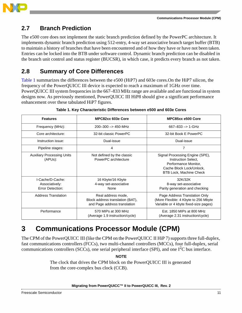
2.8 Summary of Core DifferencesTable 1 summarizes the differences between the e500 (HiP7) and 603e cores.On the HiP7 silicon, the frequency of the PowerQUICC III device is expected to reach a maximum of 1GHz over time. PowerQUICC III system frequencies in the 667–833 MHz range are available and are functional in system designs now. As previously mentioned, PowerQUICC III HiP8 should give a significant performance enhancement over these tabulated HiP7 figures.
3 Communications Processor Module (CPM)The CPM of the PowerQUICC III (like the CPM on the PowerQUICC II HiP 7) supports three full-duplex, fast communications controllers (FCCs), two multi-channel controllers (MCCs), four full-duplex, serial communications controllers (SCCs), one serial peripheral interface (SPI), and one I2C bus interface.
NOTE
The clock that drives the CPM block on the PowerQUICC III is generated from the core-complex bus clock (CCB).
Table 1. Key Characteristic Differences between e500 and 603e Cores
Features MPC82xx 603e Core MPC85xx e500 Core
Frequency (MHz): 200–300 –> 450-MHz 667–833 –> 1-GHz
Core architecture: 32-bit classic PowerPC 32-bit Book E PowerPC
Instruction issue: Dual-issue Dual-issue
Pipeline stages: 4 7
Auxiliary Processing Units (APUs):
Not defined by the classicPowerPC architecture
Signal Processing Engine (SPE),Instruction Select,
Performance Monitor,Cache Block Lock/Unlock,BTB Lock, Machine Check
I-Cache/D-Cache: Associatively:
Error Detection:
16 Kbyte/16 Kbyte4-way set-associative
None
32K/32K8-way set-associative
Parity generation and checking
Address Translation Real address mode,Block address translation (BAT),
and Page address translation
Page Address Translation Only(More Flexible: 4 Kbyte to 256 MbyteVariable or 4 kbyte fixed-size pages)
Performance 570 MIPs at 300 MHz(Average 1.9 instruction/cycle)
Est. 1850 MIPs at 800 MHz(Average 2.31 instruction/cycle)
Migrating from PowerQUICC™ II to PowerQUICC III, Rev. 2
12 Freescale Semiconductor
Communications Processor Module (CPM)
The following sections highlight the CPM differences between the PowerQUICC II HiP7 and the PowerQUICC III. Because the PowerQUICC III CPM architecture is nearly identical to the PowerQUICC II, you can use existing PowerQUICC II microcode on the PowerQUICC III CPM. However, there are differences in the interrupt handling of the e500. These differences are described in Section 4.9, “Programmable Interrupt Controller (PIC)” and Section 6.1, “Exception Handling.”
3.1 CPM Performance and Internal MemoryTo attain more CPM bandwidth on the PowerQUICC III, the CPM operates at a maximum speed of 333 MHz as opposed to 300 MHz on the PowerQUICC II (HiP7). This gives PowerQUICC III applications a notable performance improvement over similar PowerQUICC II (HiP7) designs.
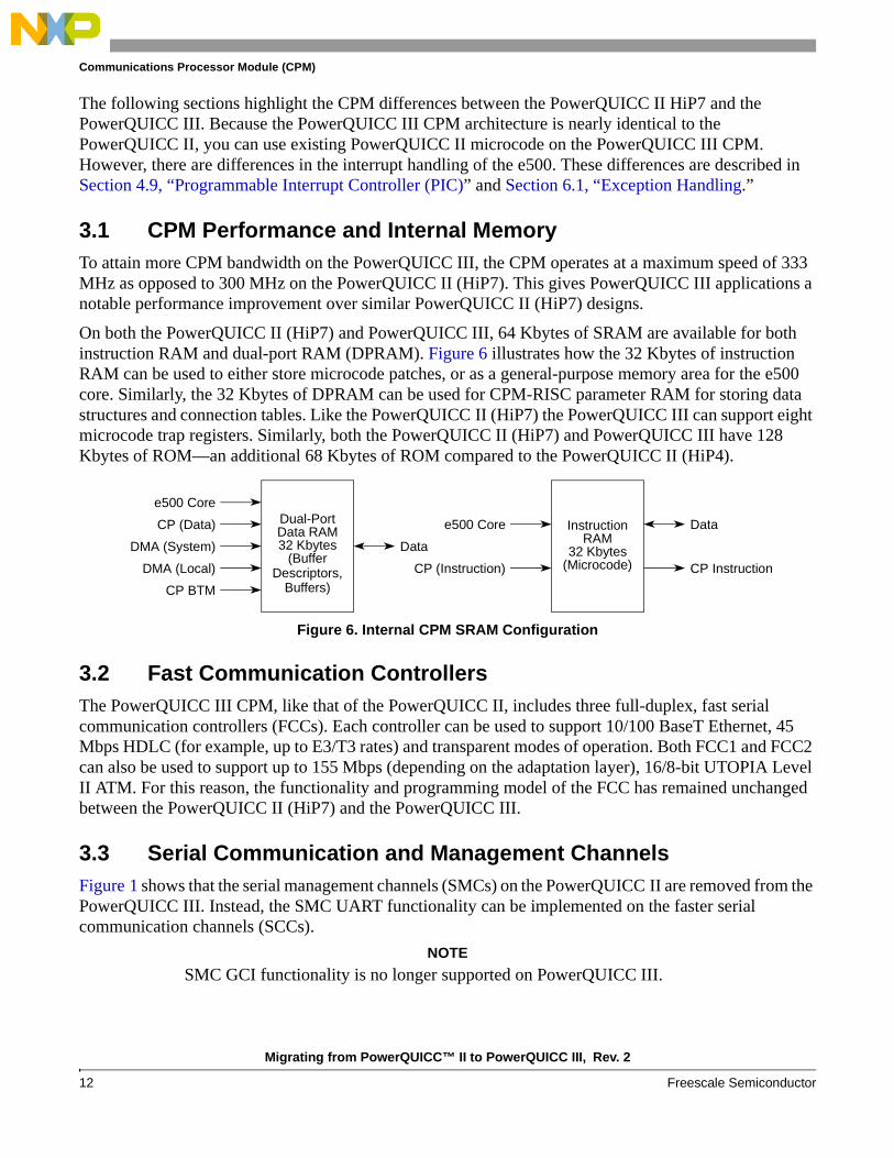
On both the PowerQUICC II (HiP7) and PowerQUICC III, 64 Kbytes of SRAM are available for both instruction RAM and dual-port RAM (DPRAM). Figure 6 illustrates how the 32 Kbytes of instruction RAM can be used to either store microcode patches, or as a general-purpose memory area for the e500 core. Similarly, the 32 Kbytes of DPRAM can be used for CPM-RISC parameter RAM for storing data structures and connection tables. Like the PowerQUICC II (HiP7) the PowerQUICC III can support eight microcode trap registers. Similarly, both the PowerQUICC II (HiP7) and PowerQUICC III have 128 Kbytes of ROM—an additional 68 Kbytes of ROM compared to the PowerQUICC II (HiP4).
Figure 6. Internal CPM SRAM Configuration
3.2 Fast Communication ControllersThe PowerQUICC III CPM, like that of the PowerQUICC II, includes three full-duplex, fast serial communication controllers (FCCs). Each controller can be used to support 10/100 BaseT Ethernet, 45 Mbps HDLC (for example, up to E3/T3 rates) and transparent modes of operation. Both FCC1 and FCC2 can also be used to support up to 155 Mbps (depending on the adaptation layer), 16/8-bit UTOPIA Level II ATM. For this reason, the functionality and programming model of the FCC has remained unchanged between the PowerQUICC II (HiP7) and the PowerQUICC III.
3.3 Serial Communication and Management ChannelsFigure 1 shows that the serial management channels (SMCs) on the PowerQUICC II are removed from the PowerQUICC III. Instead, the SMC UART functionality can be implemented on the faster serial communication channels (SCCs).
NOTE
SMC GCI functionality is no longer supported on PowerQUICC III.
Dual-PortData RAM32 Kbytes
(Buffer
e500 Core
CP (Data)
DMA (System)
DMA (Local)
CP BTM
Data
InstructionRAM
32 Kbytes(Microcode)
e500 Core
CP (Instruction)
Data
CP Instruction
Buffers)Descriptors,
Migrating from PowerQUICC™ II to PowerQUICC III, Rev. 2
Freescale Semiconductor 13
Communications Processor Module (CPM)
The function of each of the four SCCs is slightly different on the PowerQUICC III than on the PowerQUICC II. On the PowerQUICC III, the 10 BaseT Ethernet support on the SCC is removed and that functionality is now provided through one of the three FCCs, or through one of the two three-speed Ethernet controllers (TSECs), as shown in Table 2. Like the PowerQUICC II, the SCCs offer protocol support for UART, HDLC, HDLC bus, Appletalk/Localtalk, transparent, and BISYNC modes. In order to protect existing software legacy, the programming models for all of the supported protocols on the SCCs are the same as the PowerQUICC II.
3.4 Independent/Serial Direct Memory AccessIn the PowerQUICC II, the CPM contains two physical serial DMA (SDMA) channels. The CPM uses these two physical channels to implement two dedicated SDMA channels for each of the FCC, MCC, SCC, SMC, SPI and I2C. In addition, four virtual SDMA channels can be assigned to the programmable and independent DMA (IDMA) channels. On the PowerQUICC III, PPC Little-Endian SDMA mode is not supported because this mode is typically not used in a big-endian system. IDMA emulation is also not supported on the CPM because implementing SDMA or IDMA channels on the PowerQUICC II consumes valuable CPM bandwidth. On the PowerQUICC III, the introduction of a dedicated 4-channel hardware DMA engine means that channels are more efficient and can be quickly set up and removed without wasting CPM bandwidth. The IDMA features of the PowerQUICC II, as well as a number of new features, exist in the new hardware DMA block on the PowerQUICC III. See Section 4.1, “e500 Coherency Module (ECM)” for details on the 4-channel hardware DMA engine.
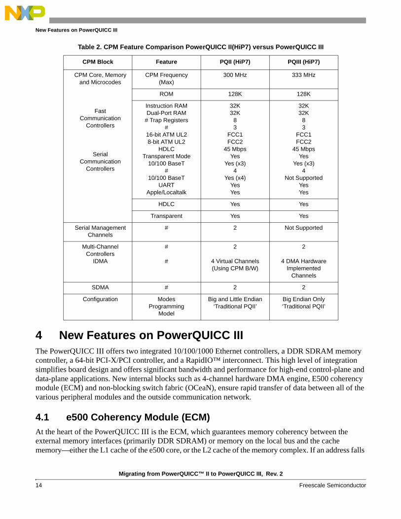
3.5 CPM SummaryThe differences between the CPM on the PowerQUICC II and PowerQUICC III lead to increased functionality and performance while retaining the existing programming model to maximize the value of your software legacy code. Table 2 summarizes the main CPM differences between the PowerQUICC II and PowerQUICC III.
Migrating from PowerQUICC™ II to PowerQUICC III, Rev. 2
14 Freescale Semiconductor
New Features on PowerQUICC III
4 New Features on PowerQUICC IIIThe PowerQUICC III offers two integrated 10/100/1000 Ethernet controllers, a DDR SDRAM memory controller, a 64-bit PCI-X/PCI controller, and a RapidIO™ interconnect. This high level of integration simplifies board design and offers significant bandwidth and performance for high-end control-plane and data-plane applications. New internal blocks such as 4-channel hardware DMA engine, E500 coherency module (ECM) and non-blocking switch fabric (OCeaN), ensure rapid transfer of data between all of the various peripheral modules and the outside communication network.
4.1 e500 Coherency Module (ECM)At the heart of the PowerQUICC III is the ECM, which guarantees memory coherency between the external memory interfaces (primarily DDR SDRAM) or memory on the local bus and the cache memory—either the L1 cache of the e500 core, or the L2 cache of the memory complex. If an address falls
Table 2. CPM Feature Comparison PowerQUICC II(HiP7) versus PowerQUICC III
CPM Block Feature PQII (HiP7) PQIII (HiP7)
CPM Core, Memory and Microcodes
Fast Communication
Controllers
Serial Communication
Controllers
CPM Frequency(Max)
300 MHz 333 MHz
ROM 128K 128K
Instruction RAMDual-Port RAM
# Trap Registers#
16-bit ATM UL28-bit ATM UL2
HDLCTransparent Mode
10/100 BaseT#
10/100 BaseTUART
Apple/Localtalk
32K32K
83
FCC1FCC2
45 MbpsYes
Yes (x3)4
Yes (x4)YesYes
32K32K
83
FCC1FCC2
45 MbpsYes
Yes (x3)4
Not SupportedYesYes
HDLC Yes Yes
Transparent Yes Yes
Serial Management Channels
# 2 Not Supported
Multi-Channel Controllers
IDMA
#
#
2
4 Virtual Channels(Using CPM B/W)
2
4 DMA HardwareImplemented
Channels
SDMA # 2 2
Configuration ModesProgramming
Model
Big and Little Endian‘Traditional PQII’
Big Endian Only‘Traditional PQII’
Migrating from PowerQUICC™ II to PowerQUICC III, Rev. 2
Freescale Semiconductor 15
New Features on PowerQUICC III
into one of the ECM-defined windows, it is forwarded to the correct destination. For example, if a buffer on the local bus is marked as snoopable, all traffic to that buffer is routed using the ECM. This ECM operation highlights the difference in the transaction style architecture of the PowerQUICC III compared to the shared bus architecture of the PowerQUICC II.
ECM transactions are not implicitly coherent. The internal bus is snooped by e500 L1 and L2 caches to maintain coherency only if the transaction across the ECM has the GBL bit set to mark it as a global transaction. If this is not the case, then the ECM is used as a simple conduit for the transaction to get to its destination. Thus, only global transactions across the ECM are coherent transactions; all others (between the CPM and the local bus, and across the on-chip fabric) are non-coherent. In reality, most internal data transfers are in some way processed by the ECM.
Inside the PowerQUICC III is a 32-bit local address mapping unit that allows 32-bit addressing structures to map to larger addressable devices completely independently, for example, 32-bit PowerQUICC III address to 64-bit PCI address. As a result, the PowerQUICC III system map normally consists of a 32-bit local address space and a larger external address space. Accessing external address space is achieved by using inbound and outbound translation windows, whereas inbound transactions use local access windows (LAWs). It is through these LAWS that the ECM knows where/how to route transactions throughout the internal PowerQUICC III architecture. Only transactions that hit a particular IBW or LAW are actually processed.
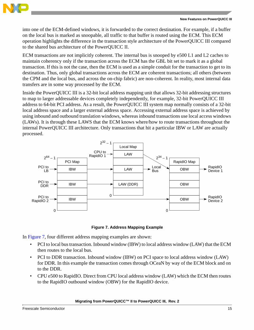
Figure 7. Address Mapping Example
In Figure 7, four different address mapping examples are shown:
• PCI to local bus transaction. Inbound window (IBW) to local address window (LAW) that the ECM then routes to the local bus.
• PCI to DDR transaction. Inbound window (IBW) on PCI space to local address window (LAW) for DDR. In this example the transaction comes through OCeaN by way of the ECM block and on to the DDR.
• CPU e500 to RapidIO. Direct from CPU local address window (LAW) which the ECM then routes to the RapidIO outbound window (OBW) for the RapidIO device.
PCI Map
IBW
IBW
IBW
RapidIO Map
OBW
OBW
OBW
Local Map
LAW
LAW
LAW (DDR)
PCI to LocalBus
RapidIODevice 1LB
PCI toDDR
PCI toRapidIO 2
RapidIODevice 2
CPU toRapidIO 1
264 – 1
0
232 – 1
0
234 – 1
0
Migrating from PowerQUICC™ II to PowerQUICC III, Rev. 2
16 Freescale Semiconductor
New Features on PowerQUICC III
• PCI to RapidIO. From PCI space inbound window (IBW) direct to RapidIO outbound window (OBW) for the RapidIO device. Here the ECM is not involved, and the transaction is simply a OCeaN port-to-port transaction, local to the OCeaN block.
The coherency module is optimized for low-latency access to the DDR memory by performing ‘speculative reads’ using a separate internal bus to the DDR controller. This speculative read starts a transaction in the DDR memory before a response from the cache is received on whether the access is actually a cache hit or not. If the access is a cache hit then the speculative read is ignored and then discarded; otherwise, if the access is a cache miss, the speculative read transaction completes and a couple of extra clock cycles have been saved.
There are two arbitration mechanisms inside the ECM, the I/O arbiter and the CCB arbiter. An I/O (for example, OCeaN, CPM or either of the two TSECs) must first compete for an internal ECM grant for the CCB with each of the other three I/Os. Arbitration can be won through either a higher priority level access or a lower priority waiting request. After arbitration is won, the winning bus request must also compete with the e500 core for CCB ownership (using the same arbitration mechanisms) before the transaction is finally entered into the transaction queue. The number of posted transactions by the winning controller is set through the EEBACR[A_STRM_CNT], which by default is set to three. As a result, by limiting the number of posted transactions, higher priority transactions or lower priority waiting requests can be arbitrated for the CCB with the minimum of delay.
4.2 DMA ControllerThe DMA controller on the PowerQUICC III is a dedicated 4-channel, independent, general-purpose controller for use by both local and remote masters to transfer data between any memory mapped area of the PowerQUICC III (for example, PCI, Local Bus, or Rio). The implementation of the DMA controller is similar to that of the IDMA implementation on the PowerQUICC II with ‘traditional’ direct/auto buffer, and chaining modes being supported. However the PowerQUICC III offers additional features as well as off-loading the main CPM from performing DMA transactions. The result is an efficient, user-configurable solution that can be controlled either internally using software or externally using the external DMA I/O pins.
4.2.1 DMA Controller Operation ModesIn addition to the direct and chaining modes of operation, the following new features are implemented in the hardware DMA block:
• Extended mode (stride capability)
• Bypass ATMU mode (RapidIO)
• External Master mode
• Channel halt/abort/continue mode
• Destination/source address hold enable mode
4.2.1.1 Extended Mode—Advanced Chaining/Stride Capability
The advanced chaining mode allows the user to set up a series of buffer descriptors referenced from a linked list. The DMA controller can then walk through multiple buffer descriptors, allowing complex
Migrating from PowerQUICC™ II to PowerQUICC III, Rev. 2
Freescale Semiconductor 17
New Features on PowerQUICC III
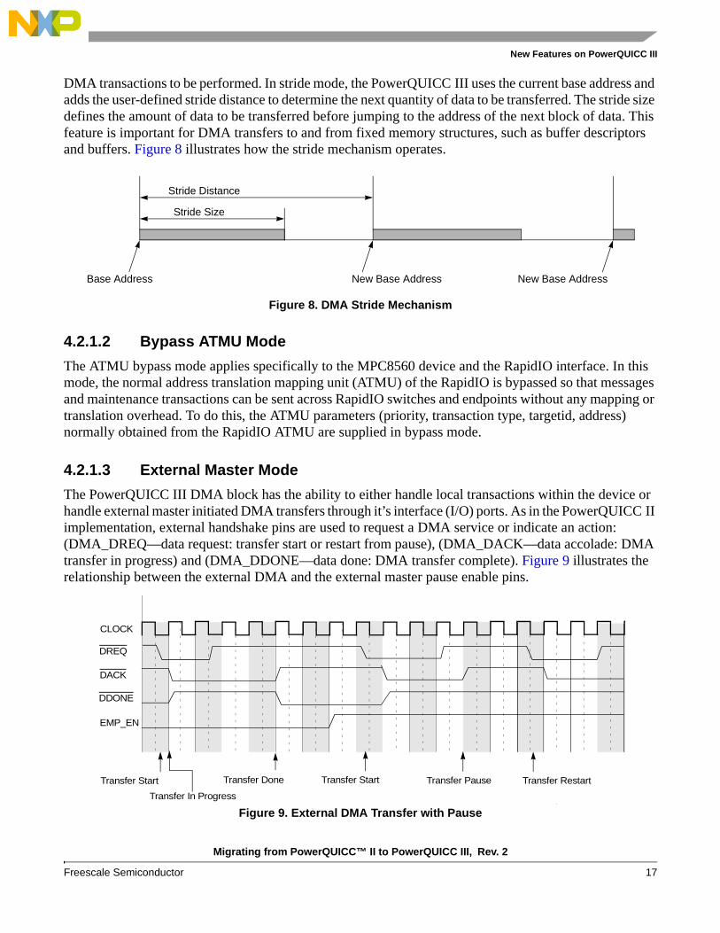
DMA transactions to be performed. In stride mode, the PowerQUICC III uses the current base address and adds the user-defined stride distance to determine the next quantity of data to be transferred. The stride size defines the amount of data to be transferred before jumping to the address of the next block of data. This feature is important for DMA transfers to and from fixed memory structures, such as buffer descriptors and buffers. Figure 8 illustrates how the stride mechanism operates.
Figure 8. DMA Stride Mechanism
4.2.1.2 Bypass ATMU Mode
The ATMU bypass mode applies specifically to the MPC8560 device and the RapidIO interface. In this mode, the normal address translation mapping unit (ATMU) of the RapidIO is bypassed so that messages and maintenance transactions can be sent across RapidIO switches and endpoints without any mapping or translation overhead. To do this, the ATMU parameters (priority, transaction type, targetid, address) normally obtained from the RapidIO ATMU are supplied in bypass mode.
4.2.1.3 External Master Mode
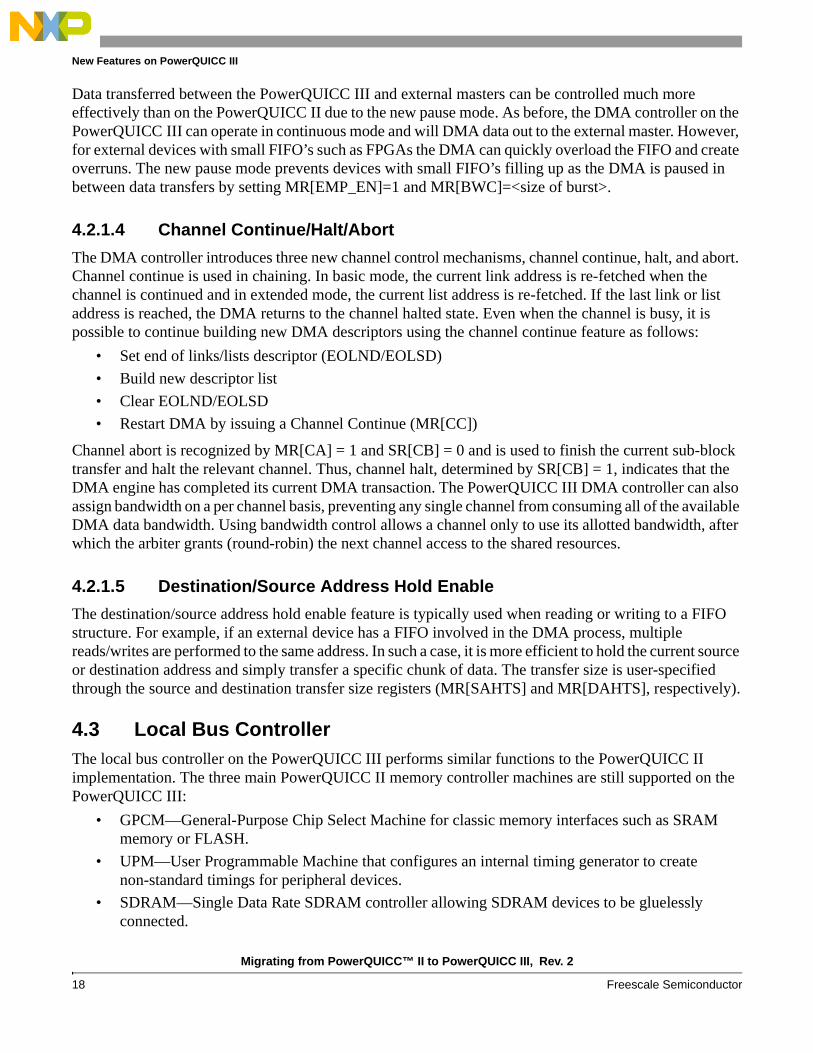
The PowerQUICC III DMA block has the ability to either handle local transactions within the device or handle external master initiated DMA transfers through it’s interface (I/O) ports. As in the PowerQUICC II implementation, external handshake pins are used to request a DMA service or indicate an action: (DMA_DREQ—data request: transfer start or restart from pause), (DMA_DACK—data accolade: DMA transfer in progress) and (DMA_DDONE—data done: DMA transfer complete). Figure 9 illustrates the relationship between the external DMA and the external master pause enable pins.
Figure 9. External DMA Transfer with Pause
Stride Size
Stride Distance
Base Address New Base Address New Base Address
DREQ
CLOCK
DACK
DDONE
Transfer Start
Transfer In Progress
Transfer Done Transfer Start Transfer Pause Transfer Restart
EMP_EN
Migrating from PowerQUICC™ II to PowerQUICC III, Rev. 2
18 Freescale Semiconductor
New Features on PowerQUICC III
Data transferred between the PowerQUICC III and external masters can be controlled much more effectively than on the PowerQUICC II due to the new pause mode. As before, the DMA controller on the PowerQUICC III can operate in continuous mode and will DMA data out to the external master. However, for external devices with small FIFO’s such as FPGAs the DMA can quickly overload the FIFO and create overruns. The new pause mode prevents devices with small FIFO’s filling up as the DMA is paused in between data transfers by setting MR[EMP_EN]=1 and MR[BWC]=<size of burst>.
4.2.1.4 Channel Continue/Halt/Abort
The DMA controller introduces three new channel control mechanisms, channel continue, halt, and abort. Channel continue is used in chaining. In basic mode, the current link address is re-fetched when the channel is continued and in extended mode, the current list address is re-fetched. If the last link or list address is reached, the DMA returns to the channel halted state. Even when the channel is busy, it is possible to continue building new DMA descriptors using the channel continue feature as follows:
• Set end of links/lists descriptor (EOLND/EOLSD)
• Build new descriptor list
• Clear EOLND/EOLSD
• Restart DMA by issuing a Channel Continue (MR[CC])
Channel abort is recognized by MR[CA] = 1 and SR[CB] = 0 and is used to finish the current sub-block transfer and halt the relevant channel. Thus, channel halt, determined by SR[CB] = 1, indicates that the DMA engine has completed its current DMA transaction. The PowerQUICC III DMA controller can also assign bandwidth on a per channel basis, preventing any single channel from consuming all of the available DMA data bandwidth. Using bandwidth control allows a channel only to use its allotted bandwidth, after which the arbiter grants (round-robin) the next channel access to the shared resources.
4.2.1.5 Destination/Source Address Hold Enable
The destination/source address hold enable feature is typically used when reading or writing to a FIFO structure. For example, if an external device has a FIFO involved in the DMA process, multiple reads/writes are performed to the same address. In such a case, it is more efficient to hold the current source or destination address and simply transfer a specific chunk of data. The transfer size is user-specified through the source and destination transfer size registers (MR[SAHTS] and MR[DAHTS], respectively).
4.3 Local Bus ControllerThe local bus controller on the PowerQUICC III performs similar functions to the PowerQUICC II implementation. The three main PowerQUICC II memory controller machines are still supported on the PowerQUICC III:
• GPCM—General-Purpose Chip Select Machine for classic memory interfaces such as SRAM memory or FLASH.
• UPM—User Programmable Machine that configures an internal timing generator to create non-standard timings for peripheral devices.
• SDRAM—Single Data Rate SDRAM controller allowing SDRAM devices to be gluelessly connected.
Migrating from PowerQUICC™ II to PowerQUICC III, Rev. 2
Freescale Semiconductor 19
New Features on PowerQUICC III
Although functionally similar, the PowerQUICC III implementation of the UPM has three dedicated UPMs unique to the local bus. On the PowerQUICC II, these UPMs are also shared with the 60x bus. Similarly, on PowerQUICC II, the twelve available chip selects must be shared with the 60x bus. On the PowerQUICC III, there are eight dedicated chip selects specific to the local bus. The ability to support bank based interleaving on the SDRAM controller on the PowerQUICC II has been removed. On the SDRAM controller on the PowerQUICC III, only page-based interleaving is supported because page-based interleaving allows a greater degree of flexibility and control when accessing connected SDRAM devices.
The major difference between the two devices is that the local bus controller on the PowerQUICC III can operate at up to 166 MHz. The maximum supported frequency on the PowerQUICC II is 100 MHz. The local bus on the PowerQUICC III runs with a fixed frequency referenced from the main system frequency, SYSCLK. The local bus controller runs synchronized with the CCB clock, so if you have the CCB running at 333 MHz then the frequency of the local bus is divided down from this to either 2:1, 4:1 or 8:1 (the 8:1 option is the default configuration from reset). The local bus also has optimized state machines to support the specific transaction size that is generated by the CPM. Therefore, a 32-bit configured local bus has minimal associated overhead when passing traffic between external peripherals and the CPM.
The local bus programming model remains the same as on the PowerQUICC II. It supports 8 chip-selects, each individually configurable to either 8, 16 or 32 bits wide. Each individual chip-select can support up to 2 Gigabytes of address space. As before, the local bus supports both natural parity and read-modify-write (RMW) data parity checking.
One difference with the local bus controller on the PowerQUICC III is that a wider range of addressable banks can be selected within a connected device due to its 34-bit address decoding, as opposed to 32-bit address decoding on the PowerQUICC II. To save pins of the PowerQUICC III design, a 32-bit multiplexed address/data interface is implemented. This is an important difference from the PowerQUICC II because any design requires an external buffer and latch combination to demultiplex the multiplexed address/data signals. The logic for controlling these external devices is integrated into the PowerQUICC III design. (On the PowerQUICC II, the local bus had 18 separate address pins and 32 data pins).
4.4 Dual Data Rate (DDR) Memory ControllerThe dual data rate (DDR) SDRAM controller is a new feature on the PowerQUICC III and currently supports DDR type 1 SDRAM at up to 333 MHz. Because DDR memory is clocked on both edges of the input clock, the actual maximum clock rate is 167 MHz. Note that the MCK# [5:0] signals are simply the inverted clocks from the MCK [5:0] signals and not true differential clock signals.
On the PowerQUICC II, the 60x bus allows users to connect to SDRAM, flash memory, and other 60x bus compatible peripherals. However, on the PowerQUICC III, the DDR controller is a dedicated 64-bit data bus (+ 8-bit ECC) with no external master capability and it is used exclusively for DDR memories as the main system bus. Connection to other external masters can be readily implemented through either the PCI or RapidIO interfaces.
Migrating from PowerQUICC™ II to PowerQUICC III, Rev. 2
20 Freescale Semiconductor
New Features on PowerQUICC III
4.4.1 Feature SummaryThe DDR controller can support discrete or DIMM DDR memories between 64 Mbit and 1 Gbit in size. The DDR controller has four chip selects to access a (theoretical) maximum of 1 Gbyte addressing space. In reality, the full 4 gigabytes cannot be used for DDR because 4 gigabytes is the maximum addressing that the whole PowerQUICC III can handle. Thus, the DDR controller is restricted through design to have a maximum addressing limit of 3.5 Gbyte to allow other connected peripherals to have space in the PowerQUICC III memory map.
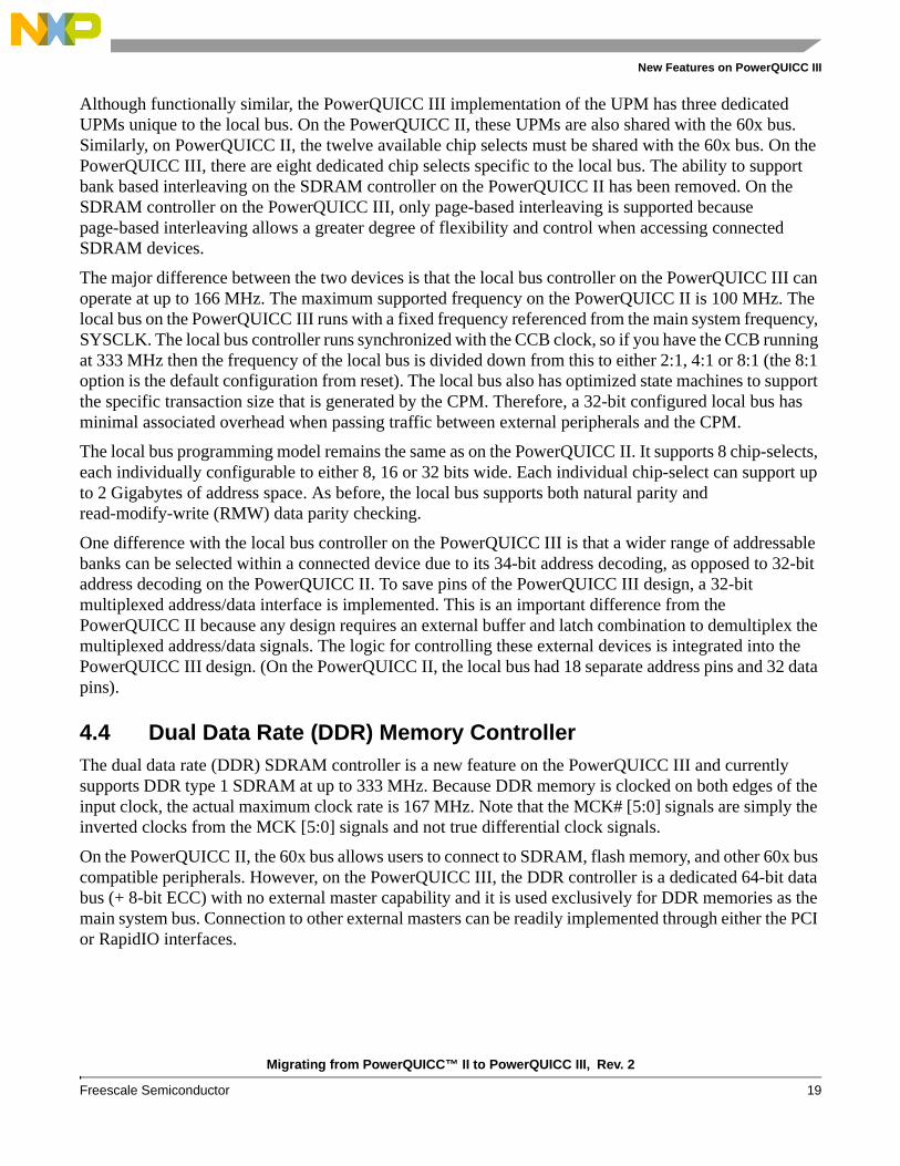
4.4.2 DLL Delay Compensation LoopBecause the PowerQUICC III operates at much higher frequencies than the PowerQUICC II, the clocks for the memory interface (the digital locked loops or DLLs) are integrated into the PowerQUICC III design. Therefore, the AC timing requirements can now be accurately optimized on a per-design basis using a PCB/layout feedback delay loop as shown in Figure 10.
Figure 10. DDR SDRAM DLL Feedback Delay
During layout of the final PCB, the layout engineer must set the length of this compensation feedback loop to be the same as clock tree on the chip. Thus, the internal DLL clock compensates for the external clock tree delay and is 100 percent aligned, allowing maximum margin on the AC timing specifications of the DDR SDRAM. Of course, this allows maximum flexibility because users can create more or less set up and hold time to suit their end system requirements.
4.4.3 Six Clock PairsIn traditional clock design, you should not supply more than three input pins with one clock. Otherwise, the resulting clock may be degraded under loaded conditions. Therefore, the DDR controller supplies six clock pairs for use with DDR memory. (Some degree of external clock buffering is additionally required if you decide to deviate from this clock design guideline).
DDR Controller DDR SDRAM
CKInternal Clock
DLL_Sync_Out
CK
DLL_Sync_InDLL
DLL
DLL TimingLoop
L2
Clock PCB Trace Length ‘L’
Migrating from PowerQUICC™ II to PowerQUICC III, Rev. 2
Freescale Semiconductor 21
New Features on PowerQUICC III
4.4.4 Sleep Mode Support for Self Refreshing SDRAMAnother feature on the DDR SDRAM controller is support for sleep mode for self refreshing SDRAM. This feature is useful if the clocks or power on the processor have to be stopped for some reason. Prior to shutting down the power to the processor, this mode executes a self refresh command to the DDR SDRAM to ensure that the DDR remains intact when it wakes up from the clock stop mode. This allows the DDR SDRAM to gracefully recover from where it was before the power/clocks were stopped.
4.4.5 Dynamic Power Management
Dynamic power management allows users to maximize the bandwidth capabilities of the DDR SDRAM by using on-the-fly power management. When the DDR transaction pipeline begins to empty, the device automatically uses the clock enable to put the device into power conservation mode. As new DDR transactions arrive, the devices comes out of power conservation mode and begins pipelining those new transactions for execution.
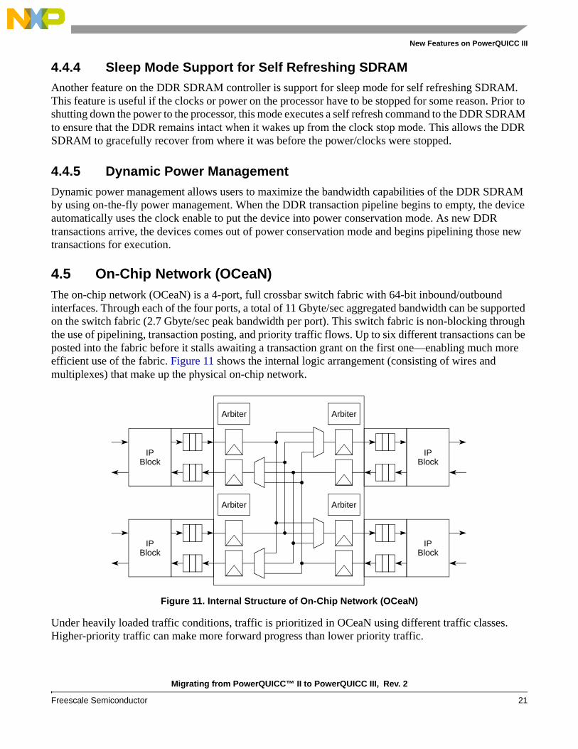
4.5 On-Chip Network (OCeaN)The on-chip network (OCeaN) is a 4-port, full crossbar switch fabric with 64-bit inbound/outbound interfaces. Through each of the four ports, a total of 11 Gbyte/sec aggregated bandwidth can be supported on the switch fabric (2.7 Gbyte/sec peak bandwidth per port). This switch fabric is non-blocking through the use of pipelining, transaction posting, and priority traffic flows. Up to six different transactions can be posted into the fabric before it stalls awaiting a transaction grant on the first one—enabling much more efficient use of the fabric. Figure 11 shows the internal logic arrangement (consisting of wires and multiplexes) that make up the physical on-chip network.
Figure 11. Internal Structure of On-Chip Network (OCeaN)
Under heavily loaded traffic conditions, traffic is prioritized in OCeaN using different traffic classes. Higher-priority traffic can make more forward progress than lower priority traffic.
IPBlock
IPBlock
Arbiter
IPBlock
IPBlock
Arbiter
Arbiter Arbiter
Migrating from PowerQUICC™ II to PowerQUICC III, Rev. 2
22 Freescale Semiconductor
New Features on PowerQUICC III
Processing deadlocks are avoided through the use of priority reordering. For example, a request can be made from a blocked port to another unblocked port to pass a blocked transaction ahead. This helps to remove head-of-line blockages when switching traffic between PCI/PCI-X, RapidIO, the DMA controller and the internal system bus.
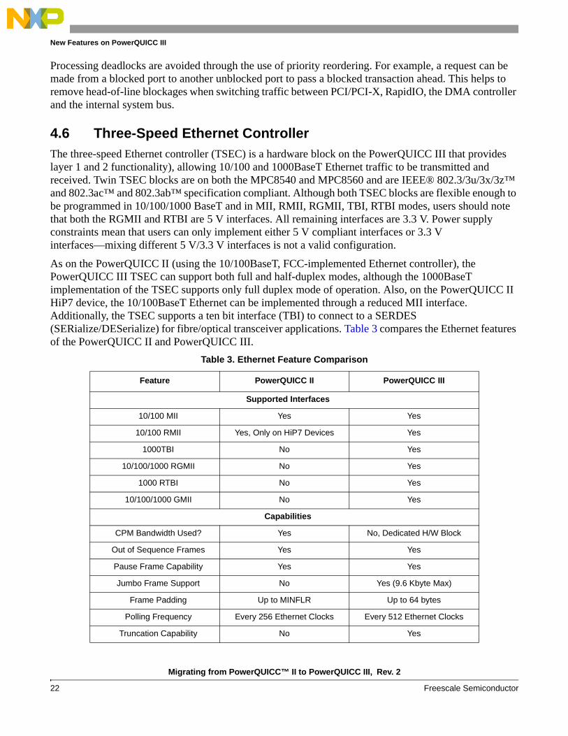
4.6 Three-Speed Ethernet ControllerThe three-speed Ethernet controller (TSEC) is a hardware block on the PowerQUICC III that provides layer 1 and 2 functionality), allowing 10/100 and 1000BaseT Ethernet traffic to be transmitted and received. Twin TSEC blocks are on both the MPC8540 and MPC8560 and are IEEE® 802.3/3u/3x/3z™ and 802.3ac™ and 802.3ab™ specification compliant. Although both TSEC blocks are flexible enough to be programmed in 10/100/1000 BaseT and in MII, RMII, RGMII, TBI, RTBI modes, users should note that both the RGMII and RTBI are 5 V interfaces. All remaining interfaces are 3.3 V. Power supply constraints mean that users can only implement either 5 V compliant interfaces or 3.3 V interfaces—mixing different 5 V/3.3 V interfaces is not a valid configuration.
As on the PowerQUICC II (using the 10/100BaseT, FCC-implemented Ethernet controller), the PowerQUICC III TSEC can support both full and half-duplex modes, although the 1000BaseT implementation of the TSEC supports only full duplex mode of operation. Also, on the PowerQUICC II HiP7 device, the 10/100BaseT Ethernet can be implemented through a reduced MII interface. Additionally, the TSEC supports a ten bit interface (TBI) to connect to a SERDES (SERialize/DESerialize) for fibre/optical transceiver applications. Table 3 compares the Ethernet features of the PowerQUICC II and PowerQUICC III.
Table 3. Ethernet Feature Comparison
Feature PowerQUICC II PowerQUICC III
Supported Interfaces
10/100 MII Yes Yes
10/100 RMII Yes, Only on HiP7 Devices Yes
1000TBI No Yes
10/100/1000 RGMII No Yes
1000 RTBI No Yes
10/100/1000 GMII No Yes
Capabilities
CPM Bandwidth Used? Yes No, Dedicated H/W Block
Out of Sequence Frames Yes Yes
Pause Frame Capability Yes Yes
Jumbo Frame Support No Yes (9.6 Kbyte Max)
Frame Padding Up to MINFLR Up to 64 bytes
Polling Frequency Every 256 Ethernet Clocks Every 512 Ethernet Clocks
Truncation Capability No Yes
Migrating from PowerQUICC™ II to PowerQUICC III, Rev. 2
Freescale Semiconductor 23
New Features on PowerQUICC III
As in the FCC Ethernet controller (100BaseT) on the PowerQUICC II, the TSEC block supports both internal and external loopback. However, users should note that internal loopback on the PowerQUICC III is supported only in GMII, MII or TBI modes—no internal loopback is supported when the controller is configured in RGMII or RTBI mode. As on the PowerQUICC II, external loopback is performed at the interface pins. On the PowerQUICC II, 64-bits are available for address hash matching; on the PowerQUICC III TSEC implementation, hash matching bits are extended to 256 bits so a greater range of addresses can be decoded.
Due to the high bit rates, the TSEC has hidden operating modes to internally manage its FIFOs to help avert either underrun or overrun conditions. Entering internal TSEC starve mode is an indication that the Tx FIFO is in danger of under-running. When the FIFO nears empty (within 0.5 Kbytes), the starve state is entered and the ECM automatically increases the priority of the internal DMA and also that of the TSEC block to avert the underrun. When the FIFO fills back up to within 1 Kbyte of empty, starve mode is shut off. Similarly, for frame reception, when the 2-Kbytes internal FIFO reaches the 1-Kbyte level, an internal panic alarm raises the priority of the TSEC block to avoid an overrun. If the FIFO continues to fill, then at the 1.5 Kbytes full level, an emergency panic increases the DMA priority to its maximum and sends a PAUSE frame so that the data already received can be processed before other data is received.
Another useful feature is the ability to contour the behavior of the TSEC with regard to frame interrupts on both transmitted and received frames. This feature is known as interrupt coalescing and can use either a frame counting or timer threshold method. In the frame counting implementation, the user can configure frame interrupts as deliberately grouped to reduce the number of raised interrupts, thereby avoiding interrupts bandwidth congestion due to frequent consecutive interrupts. Similarly, stale frame interrupts can be avoided using the timer threshold approach, beyond which frame interrupts not yet raised are forced. This is an important feature for helping to optimize packet processing of TSEC frames by the core.
The PowerQUICC III TSEC programming model is backwards-compatible with the PowerQUICC II. As in the PowerQUICC II, the TSEC transfers data into and out off buffers to which buffer descriptors and connection tables point. This helps ensure that any legacy software is retained.
4.7 PCI/PCI-XThe PCI interface on the PowerQUICC III is the same functional block as on the PowerQUICC II and is version 2.2 compliant, supporting transaction speeds between 16 to 66MHz. As on the PowerQUICC II device, the PowerQUICC III PCI controller can either use its internal arbiter to control PCI transactions or an external arbiter. The PowerQUICC III PCI interface can be configured to operate either as an agent or host or configured as a master or slave PCI device. As a master device, the PowerQUICC III PCI controller manages both memory and I/O transactions, whereas as configured as a slave device, only memory transactions are controlled.
In addition to PCI support, the PowerQUICC III has a new feature which implements the PCI-X standard (version 1.0A) and can support frequencies up to 133MHz. It is perhaps useful to review the standard PCI
Supported Modes OOS, Pause OOS, Wait & Pause
Graceful Rx Stop No Yes
Internal FIFOs No – Uses DPRAM Yes – 2KB on Board
Table 3. Ethernet Feature Comparison (continued)
Migrating from PowerQUICC™ II to PowerQUICC III, Rev. 2
24 Freescale Semiconductor
New Features on PowerQUICC III
bus architecture that is available on both the PowerQUICC II and the PowerQUICC III, before looking at the actual differences between the PCI and PCI-X interface.
The PCI bus architecture is a hierarchical, multi-master arbitration scheme that uses either 32 or 64-bit addressing to post transactions onto the PCI bus. Transactions can be either accepted, retried or deferred. In the later two cases, the master repeats any transaction that needs to be retried and deferred transactions can be accepted and started by the target whilst the master retries the transaction. Since the PowerQUICC III has five different pairs of Request/Grant pairs, up to five external PCI masters can be supported. It is also worth noting that the PCI interface on the PowerQUICC III is a dedicated interface and does not multiplex its pins with other functional blocks as it did on the PowerQUICC II. The PowerQUICC II Local Bus pins and PCI were multiplexed and allowed the use of one interface or the other, for example, local bus or PCI, but not both. This restriction has now been removed on PowerQUICC III.
The performance of the PCI interface is enhanced by the two level round-robin arbitration algorithm used in the arbiter and through the ability to do mirror and pre-fetched PCI read accesses. Whilst the PCI interface supports both inbound and outbound data streaming the amount of data that can actually be streamed is limited by both the depth of pre-fetching and the target disconnect limit of the PCI specification. On the PowerQUICC III this disconnect will occur after two cache lines (i.e. after 32 bytes). This helps prevent PCI devices from hogging the bus, thus avoiding system bottlenecks and interface starvation, when operating high speed interfaces such as RapidIO or Gigabit Ethernet.
The main difference between the PCI block implemented on the PowerQUICC II to that of the PowerQUICC III is that the PowerQUICC II implements a 32-bit addressable PCI interface and can only support three Request/Grant signal pairs i.e. only a maximum of three external PCI masters can be supported. Apart from these additional address and Request/Grant signals, all other PCI signals implemented on the PowerQUICC II remain the same on PowerQUICC III.
4.7.1 PCI & PCI-X System DifferencesPerhaps the most obvious difference between PCI and PCI-X is the speed increase of the interface which can now run up to 133MHz. PCI-X is a latch-to-latch based protocol which allows more timing margin for propagation delay and receiver logic. This is shown below in Figure 12.
Figure 12. PCI/PCI-X Timing Analysis
PropDelay
ReceiverLogic
ReceiverResponds
TransmitterAssertsSignal
PropDelay
TransmitterAssertsSignal
ReceiverSamples
ReceiverLogic
ReceiverResponds
PCI
PCI-X
Migrating from PowerQUICC™ II to PowerQUICC III, Rev. 2
Freescale Semiconductor 25
New Features on PowerQUICC III
Unlike the PCI specification, PCI-X is a split transaction based protocol which has separate arbitration transactions for both bus request and response. Again, this helps to improve bus latency and utilization. Since the maximum transaction size in a PCI-X system is limited to 4K bytes, the worst case system latency dramatically improves. Also, bus utilization is improved by the restriction of both targets and initiators in inserting wait states. Targets cannot insert wait states after the first data beat and both initiators and targets can only end a burst on a naturally aligned 128-byte boundary. Each transaction in a PCI-X system carries a byte count and the identity of the initiator that was not possible in the PCI specification. Hence, PCI-X systems offer better buffer management capabilities and make more efficient use of the available system memory.
Figure 13. PCI/PCI-X System Comparison
Figure 13 illustrates the improved system performance and maximum slot capability between PCI and PCI-X systems.
4.8 RapidIORapidIO is a packet-switched technology used for high speed point-to-point bus interconnect, compliant to Rev 1.2 of the RapidIO specification. The PowerQUICC III is the first PowerQUICC family device (and the first device to market) to incorporate an integrated 8-bit RapidIO controller. Hence, this is a completely new functional block currently implemented only on the PowerQUICC III family of devices, and not a supported feature on PowerQUICC II. The RapidIO specification is divided into three different specification layers: logical, transport and physical. RapidIO networks are built around two basic system building blocks—RapidIO endpoints and switches. RapidIO endpoints as the name suggests create and consume RapidIO messages with the RapidIO switches simply passing packets between its different ports without interpreting them. Figure 14 illustrates a typical RapidIO network.
PCIWidth
PCIFrequency
PCIBandwidth
PCISlots
PCI-XSlots
32-bit 33 MHz 133 MB/s
64-bit
64-bit
64-bit
66 MHz
100 MHz
133 MHz
528 MB/s
800 MB/s
1066 MB/s
N/A
N/A
N/A
Migrating from PowerQUICC™ II to PowerQUICC III, Rev. 2
26 Freescale Semiconductor
New Features on PowerQUICC III
Figure 14. A Simple RapidIO Network
The RapidIO physical specification on the PowerQUICC III has an 8 bit wide bus that uses low-voltage differential signaling (LVDS) I/Os. Since RapidIO uses source synchronous double data rates, it can be run at 500 MHz clock which can generate 1 Gigabit per pin pair i.e. running an 8-bit wide end-point, up to 1 Gigabit per second/per pair can be received/transmitted concurrently. In order to ensure maximum data throughput, the RapidIO implementation on the PowerQUICC III supports four priority levels.
In the transportation specification, each RapidIO endpoint transmits 256-byte transaction packets which can be controlled by atomic packet semaphores i.e. increment, decrement, set and clear. In addition to these functions, RapidIO also has a messaging unit containing one inbound and one outbound data structure. Each message, or telegram can be up to 4 Kbytes in size (i.e. a total of 16 packets at 256 bytes per packet). Efficient system operation can be created using these telegrams to inform endpoints of a particular task to be performed.
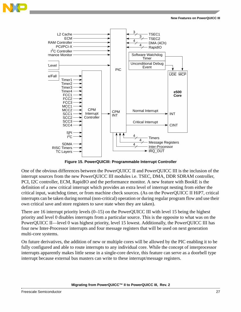
4.9 Programmable Interrupt Controller (PIC)On the current version of PowerQUICC III all interrupts are routed via the programmable interrupt controller (PIC) to the e500 core. One of the key design goals of the PIC was to ensure consistency and maximize existing PowerQUICC software legacy by cascading the PowerQUICC II CPM interrupt controller with that of the PowerQUICIII PIC.
A diagram of the PowerQUICC III PIC is shown in Figure 15.
Port 3 Port 1Endpoint Port 3
Port 0
Endpoint Endpoint
Port 0
Port 2
Endpoint
Port 2
CPUEndpoint
Switch Switch Endpoint
DRAMPort 1
ROM
Migrating from PowerQUICC™ II to PowerQUICC III, Rev. 2
Freescale Semiconductor 27
New Features on PowerQUICC III
Figure 15. PowerQUICIII: Programmable Interrupt Controller
One of the obvious differences between the PowerQUICC II and PowerQUICC III is the inclusion of the interrupt sources from the new PowerQUICC III modules i.e. TSEC, DMA, DDR SDRAM controller, PCI, I2C controller, ECM, RapidIO and the performance monitor. A new feature with BookE is the definition of a new critical interrupt which provides an extra level of interrupt nesting from either the critical input, watchdog timer, or from machine check sources. (As on the PowerQUICC II HiP7, critical interrupts can be taken during normal (non-critical) operation or during regular program flow and use their own critical save and store registers to save state when they are taken).
There are 16 interrupt priority levels (0–15) on the PowerQUICC III with level 15 being the highest priority and level 0 disables interrupts from a particular source. This is the opposite to what was on the PowerQUICC II—level 0 was highest priority, level 15 lowest. Additionally, the PowerQUICC III has four new Inter-Processor interrupts and four message registers that will be used on next generation multi-core systems.
On future derivatives, the addition of new or multiple cores will be allowed by the PIC enabling it to be fully configured and able to route interrupts to any individual core. While the concept of interprocessor interrupts apparently makes little sense in a single-core device, this feature can serve as a doorbell type interrupt because external bus masters can write to these interrupt/message registers.
Timer1Timer2Timer3Timer4FCC1FCC2FCC3MCC1MCC2SCC1SCC2SCC3SCC4
SPII2C
SDMARISC Timers
TC Layers
CPMInterrupt
Controller
ge/Fall
Normal Interrupt
Unconditional Debug
Software Watchdog
Event
Timer
UDE MCP
e500Core
PICll/Level
L2 CacheECM
DRAM ControllerPCI/PCI-X
I2C Controllerformance Monitor
3
43
4
TSEC1TSEC2DMA (4Ch)RapidIO
CPMINT
Critical Interrupt
TimersMessage RegistersInter-ProcessorIRQ_OUT
44
4
INT
CINT
Migrating from PowerQUICC™ II to PowerQUICC III, Rev. 2
28 Freescale Semiconductor
Initialization, Reset and Boot Procedures
4.10 Enhanced Debug FeaturesThe PowerQUICC III has new debug features that include a built-in performance monitoring mechanism. The performance monitoring can be split into two distinct functions: the e500 core performance monitor and the main PowerQUICC III system performance monitor. The e500 core performance monitor consists of 32-bit counters that can be cascaded to count up to 4 of 89 defined core events, for example, branches, and cache hits/misses. Access to these performance monitor counters is achieved through two performance monitoring instructions: mtpmr and mfpmr (move to/from performance monitoring register).
The PowerQUICC III system performance monitor makes eight 32-bit counters available for general system monitoring with up to 64 system events counted on any one of these event counters. An additional 64-bit counter is also available for larger counting cycles. The user can monitor up to 576 system events, including reads or writes from DMA/RapidIO/PCI, ECM dispatch events, dropped/accepted frames, and so on. Also, the configurable CLK_OUT signal allows the user to select whether the platform (CCB) or main system clock (SYSCLK) is available on an external pin for further debug. Users can select this option through the clock out control register (CLKOCR) as detailed in the MPC85xx reference manual.
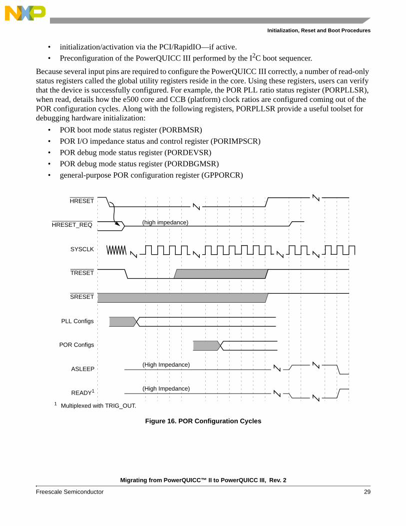
5 Initialization, Reset and Boot ProceduresPowerQUICC I and II users are familiar with the hard reset configuration word (RSTCONF) to determine the device configuration while PORESET changes from assertion to negation. On the PowerQUICC III, the POR configuration stage is a little different. This section examines the different initialization, reset, and boot procedures of the PowerQUICC III.
5.1 POR ConfigurationPerhaps the biggest difference between power on reset (POR) between the PowerQUICC II and the PowerQUICC III is the removal of the bidirectional HRESET and PORESET pins on the PowerQUICC III. When the SRESET pin on the PowerQUICC II is asserted, the processor drives it for 512 clock cycles before it is released and the SRESET flow is exited. On the PowerQUICC III, the function of the SRESET pin is different. When asserted, it causes a machine check exception (mcp) assertion to the core and also a reset to the CPM.
On the PowerQUICC III, when HRESET is asserted, various device functions are enabled by pulling certain input pins high or low through external pull-up or pull-down resistors or using configurable tri-state buffers. All logic on the chip is powered by VDD, only the I/Os reference G/L/OVDD. (Ideally, VDD and AVDD should be either powered up simultaneously or before the other chip power supplies).
After these configuration inputs are valid for at least four clock cycles, the core negates the HRESET signal and the CPM PLL and e500 DLLs begin to lock. After the DLLs are locked, the boot sequencer (if enabled) is released and can load its configuration data. The PowerQUICC III then enters the ready state and the e500 core indicates this to the external world by the negation of the ASLEEP signal and assertion of the READY signal. Chapter 4 of the MPC8560 (MPC8540) reference manual lists all the relevant configuration pins and the complete reset procedure. After the PowerQUICC III has come out of reset and the system DLLs have locked, the boot process can begin as configured by the configuration information supplied by the user. This can take the form of:
• e500 boot—if configured.
Migrating from PowerQUICC™ II to PowerQUICC III, Rev. 2
Freescale Semiconductor 29
Initialization, Reset and Boot Procedures
• initialization/activation via the PCI/RapidIO—if active.
• Preconfiguration of the PowerQUICC III performed by the I2C boot sequencer.
Because several input pins are required to configure the PowerQUICC III correctly, a number of read-only status registers called the global utility registers reside in the core. Using these registers, users can verify that the device is successfully configured. For example, the POR PLL ratio status register (PORPLLSR), when read, details how the e500 core and CCB (platform) clock ratios are configured coming out of the POR configuration cycles. Along with the following registers, PORPLLSR provide a useful toolset for debugging hardware initialization:
• POR boot mode status register (PORBMSR)
• POR I/O impedance status and control register (PORIMPSCR)
• POR debug mode status register (PORDEVSR)
• POR debug mode status register (PORDBGMSR)
• general-purpose POR configuration register (GPPORCR)
Figure 16. POR Configuration Cycles
SYSCLK
HRESET
TRESET
SRESET
(high impedance)HRESET_REQ
POR Configs
PLL Configs
READY1
ASLEEP(High Impedance)
(High Impedance)
1 Multiplexed with TRIG_OUT.
Migrating from PowerQUICC™ II to PowerQUICC III, Rev. 2
30 Freescale Semiconductor
Software Considerations
5.2 System Reset DifferencesAt reset, the PowerQUICC III behaves differently than the PowerQUICC II. The time at which the PowerQUICC III is brought out of reset can either be controlled normally; that is, during initial power-up, or it can be controlled as an agent from either the PCI or RapidIO interface.
Unlike the 603e core on the PowerQUICC II, the e500 core does not have a reset vector. Instead, the e500 core begins its execution at a fixed virtual address in its memory map at location 0xFFFFFFFC, which should be a branch instruction to the beginning address of the page mapped through TLB1. Although the e500 core begins executing in virtual mode rather than the real mode of the 603e core, the MMUs can still be set up to provide real mode addressing where the effective address equals the physical address. For information on how the hardware initialized TLB can be set up, see Section 2.5, “Memory Management.” Initialization code in this page should set up more valid TLB entries (and pages) so that the program can actually branch out of this 4-Kbyte page into other pages for booting the operating system. Similarly, the interrupt vector area and pages that contain the interrupt handlers should be set up so that exceptions can be handled early.
5.3 Boot SequencerOn the PowerQUICC III, the boot sequencer is part of the I2C block and is used before any boot code is loaded to change the default values of internal or external registers in any memory-mapped address. However, in most designs, this block is used to pre-program the PowerQUICC III to boot directly from memory devices such as burstable flash memory, DDR, or L2 cache (when configured as L2 SRAM). However, PowerQUICC II processors can boot only devices attached to the 60x bus using chip-select 0 (CS0).
This block also contains a programmable clock divider to vary its speed anywhere from 160 to 32768 CCB cycles. When this block runs in boot sequencer mode (which is determined during the initialization procedure through the LGPL3/5 inputs), any register in external memory can be modified by setting the alternate configuration space (ACS) bit and a supplying a register memory address, to which the ALTCBAR register then points. By combining the base address in the ALTCBAR with that of the 20 bits of address offset supplied from the serial ROM, you can generate a 32-bit address that is mapped to the target specified in ALTCAR. Thus, by configuring these registers, the boot sequencer has access to the entire memory map one 1-Mbyte block at a time.
6 Software ConsiderationsThe e500 core differs from the 603e core used in other PowerPC embedded devices. These differences lie mainly in supervisor mode resources. You must make small changes to initialization code when moving from the 603e core to the e500 core, but the main application code should not need to be modified. Most supervisor-related code has already been addressed by Freescale’s software third parties; often, simply recompiling with an e500-compliant compiler is all that is required.
The main areas requiring changes are around the exception handling, memory subsystem and MMU set up differences of the core. Most user mode software written on the 603e core can run unchanged on the e500 core. The only differences surround string instructions and APU specific instructions. Generally, porting code to the new e500 core does not involve major effort.
Migrating from PowerQUICC™ II to PowerQUICC III, Rev. 2
Freescale Semiconductor 31
Software Considerations
One of the main differences in running application code on the e500 core is that string instructions are no longer supported, namely: Load String word Immediate (lswi), Load String Word Indexed (lswx), Store String Word Immediate (stswi) and Store String Word indexed (stswx). The operating systems of most of the third-party software vendors for the PowerQUICC III provide trap emulation when a string instruction is encountered in compiled code, which handles this problem for the end user.
6.1 Exception HandlingThe e500 core uses interrupt prefixing and offset registers to set each individual exception vectors. When code is migrated to the e500 core from the 603e core, each exception can be set to the same vector offsets as on the 603e to ensure compatibly.
Machine check handlers also need to be rewritten because the e500 core uses a new return from machine check instruction (RFMCI) and the two machine check save and restore registers called MCSRR0 and MCSRR1. Normally, the machine check interrupt handler routine should be rewritten for the e500 core so that it exits with this new rfmci instruction.
Some special-purpose registers (SPRs) for acquiring exception information are also different. Most of this information is combined into the new e500 exception syndrome register (ESR). A machine check syndrome register (MCSR) is used to log the cause of the machine check, and the ESR is used to determine the status. Software can easily overcome this by pointing the e500 exception vectors to a different address from the 603e vector addresses so that each vector can gather the relevant system information before jumping to the common (e500/603e) code. On the 603e core, the data storage interrupt status register (DSISR) is used for this function.
Timer exceptions are compatible between the e500 and 603e core except that the decrementer does not count pass 0 on the e500. The e500 core also has a new decrementer auto reload feature that can be disabled for compatibility with the 603e core.
6.2 e500 ABITo make it easy to link existing 603e (or classic PowerPC) object files, an e500 application binary interface (ABI) is available and is used by all the leading third parties implementing e500-based tools. This ABI is necessary because there is no support on the 603e ABI for floating-point registers, 64-bit SPE registers, or embedded support. The e500 ABI specifies low-level system information such as stack usage and calling conventions as well as object file formats, linking, support of standard libraries, and program loading.
6.3 SPE APU, Floating-Point SupportThe e500 has floating-point capability using the signal processing engine (SPE) auxiliary processing unit (APU). This unit is an embedded friendly version and uses the 64-bit simple and multiple execution units as well as the 64-bit load/store unit to perform all of the necessary arithmetic manipulations with single precision. The PowerQUICC III implements floating-point operation using general-purpose registers (GPRs) instead of floating-point registers (FPRs) or vector registers (VRs). See Figure 2 for details on the e500 core complex.
The SPE APU and signal processing floating-point (SPFP) functionality is implemented on the MPC8540, the MPC8560, and all future derivatives of PowerQUICC III devices. However, these floating-point
Migrating from PowerQUICC™ II to PowerQUICC III, Rev. 2
32 Freescale Semiconductor
Software Considerations
instructions are not supported in devices subsequent to PowerQUICC III. It is strongly recommended that use of these floating-point instructions be confined to libraries and device drivers. When using SPE floating-point instructions, users should not implement them using assembly code instructions but rather include the libmoto library file. You therefore protect future software legacy by simply referring to a single file rather than complete code rewriting on devices subsequent to the PowerQUICC III.
The libmoto library is a series of hand-optimized library files specifically designed to get maximum performance when running frequently used software routines in different applications. For example, if we compare the Dhrystone benchmark for a standard optimized library, typically a value of 1.693 MIPS/MHz is obtained. Using the libmoto_e500, this performance can be considerably increased to 2.507 MIPS/MHz.
6.4 Migrating Between ADS platformsIf you use the PowerQUICC I and II, you should already be familiar with the application development system (or ADS) for software/system bring-up. The PowerQUICC III continues this tradition with the PQ3 ADS-Pilot board, which enables all features of the PowerQUICC III to be tested—for example, TSEC, RapidIO, PCI, DDR, RS-232, and 10/100BaseT Ethernet.
This section discusses the necessary switch/jumper settings when testing code originally running on the PQ2ADS, onto a PQ3ADS-Pilot. The PQ3ADS-Pilot board has a number of switches and jumpers to ensure maximum user configurability. Refer to the PowerQUICC III Application Development System Quick Reference Guide supplied with your ADS board for full details and positioning of each switch.
6.5 Fast Ethernet ConfigurationTo enable Fast Ethernet (100BaseT) MII, legacy mode, the following jumpers should be set:
• SW4 [bit 5] Enable FETH2. Set this bit.
• SW4 [bit 6] Enable FETH3. Set this bit.
• Jumper 22 FETH2. Select Legacy mode. Position jumper between terminals 1 and 2.
• Jumper 23 FETH3. Select Legacy mode. Position jumper between terminals 1 and 2.
• Jumper 31 FETH2. Select MII mode. Position jumper between terminals 1 and 2.
• Jumper 22 FETH3. Select MII mode. Position jumper between terminals 1 and 2.
Each of the two fast Ethernet PHYs have an associated PHY address that must be defined to read and write to the MII. The respective PHY addresses for FETH2 and FETH3 are 0x02 and 0x03. To read and write to the MII, these addresses must be set in the 5-bit PHY address field (bits 19–23) of the MII management address register (MIIMADD).
The fast Ethernet PHYs on the ADS-Pilot board use the Davicom DM9161 10/100 Mbps physical layer transceiver chip. To allow the transceiver to auto negotiate properly, the following DM9161 registers still need to be set: reg 16. = 0x0610.
• Aux. config. set (De)Scrambler for normal operation. The (de)scrambler is configured to bypass mode by the power-on reset latch: reg 00. = 0x1200.
• Control register autonegotiation enable/restart autonegotiation.
Migrating from PowerQUICC™ II to PowerQUICC III, Rev. 2
Freescale Semiconductor 33
Summary
7 SummaryThis document presents considerations for migrating from PowerQUICC II to PowerQUICC III. Although a number of new system blocks, as well as a new processor core, are added to the PowerQUICC III, much of the existing PowerQUICC II hardware knowledge and software legacy equally applies to the PowerQUICC III. The PowerQUICC III continues the PowerQUICC family tradition of delivering high performance, next-generation solutions for tomorrow’s leading-edge applications.

Migrating from PowerQUICC™ II to PowerQUICC III, Rev. 2
34 Freescale Semiconductor
Summary
THIS PAGE INTENTIONALLY LEFT BLANK

Migrating from PowerQUICC™ II to PowerQUICC III, Rev. 2
Freescale Semiconductor 35
Summary
THIS PAGE INTENTIONALLY LEFT BLANK
Document Number: AN2662Rev. 201/2007
Information in this document is provided solely to enable system and software
implementers to use Freescale Semiconductor products. There are no express or
implied copyright licenses granted hereunder to design or fabricate any integrated
circuits or integrated circuits based on the information in this document.
Freescale Semiconductor reserves the right to make changes without further notice to
any products herein. Freescale Semiconductor makes no warranty, representation or
guarantee regarding the suitability of its products for any particular purpose, nor does
Freescale Semiconductor assume any liability arising out of the application or use of
any product or circuit, and specifically disclaims any and all liability, including without
limitation consequential or incidental damages. “Typical” parameters which may be
provided in Freescale Semiconductor data sheets and/or specifications can and do
vary in different applications and actual performance may vary over time. All operating
parameters, including “Typicals” must be validated for each customer application by
customer’s technical experts. Freescale Semiconductor does not convey any license
under its patent rights nor the rights of others. Freescale Semiconductor products are
not designed, intended, or authorized for use as components in systems intended for
surgical implant into the body, or other applications intended to support or sustain life,
or for any other application in which the failure of the Freescale Semiconductor product
could create a situation where personal injury or death may occur. Should Buyer
purchase or use Freescale Semiconductor products for any such unintended or
unauthorized application, Buyer shall indemnify and hold Freescale Semiconductor
and its officers, employees, subsidiaries, affiliates, and distributors harmless against all
claims, costs, damages, and expenses, and reasonable attorney fees arising out of,
directly or indirectly, any claim of personal injury or death associated with such
unintended or unauthorized use, even if such claim alleges that Freescale
Semiconductor was negligent regarding the design or manufacture of the part.
How to Reach Us:
Home Page: www.freescale.com
Web Support: http://www.freescale.com/support
USA/Europe or Locations Not Listed: Freescale Semiconductor, Inc.Technical Information Center, EL5162100 East Elliot Road Tempe, Arizona 85284 +1-800-521-6274 or+1-480-768-2130www.freescale.com/support
Europe, Middle East, and Africa:Freescale Halbleiter Deutschland GmbHTechnical Information CenterSchatzbogen 781829 Muenchen, Germany+44 1296 380 456 (English) +46 8 52200080 (English)+49 89 92103 559 (German)+33 1 69 35 48 48 (French) www.freescale.com/support
Japan: Freescale Semiconductor Japan Ltd. HeadquartersARCO Tower 15F1-8-1, Shimo-Meguro, Meguro-ku Tokyo 153-0064Japan 0120 191014 or+81 3 5437 [email protected]
Asia/Pacific: Freescale Semiconductor Hong Kong Ltd. Technical Information Center2 Dai King Street Tai Po Industrial Estate Tai Po, N.T., Hong Kong +800 2666 [email protected]
For Literature Requests Only:Freescale Semiconductor
Literature Distribution Center P.O. Box 5405Denver, Colorado 80217 +1-800 441-2447 or+1-303-675-2140Fax: +1-303-675-2150LDCForFreescaleSemiconductor
@hibbertgroup.com
Freescale™ and the Freescale logo are trademarks of Freescale Semiconductor, Inc. The Power Architecture and Power.org word marks and the Power and Power.org logos and related marks are trademarks and service marks licensed by Power.org. IEEE nnn, nnn,nnn, and nnn are registered trademarks of the Institute of Electrical and Electronics Engineers, Inc. (IEEE). This product is not endorsed or approved by the IEEE. All other product or service names are the property of their respective owners.
© Freescale Semiconductor, Inc., 2007. All rights reserved.


![Compaq Armada E500 V300[1]](https://img.pdfslide.us/doc/110x75/577d1f4e1a28ab4e1e90511a/compaq-armada-e500-v3001.jpg)