Embed Size (px)
Citation preview
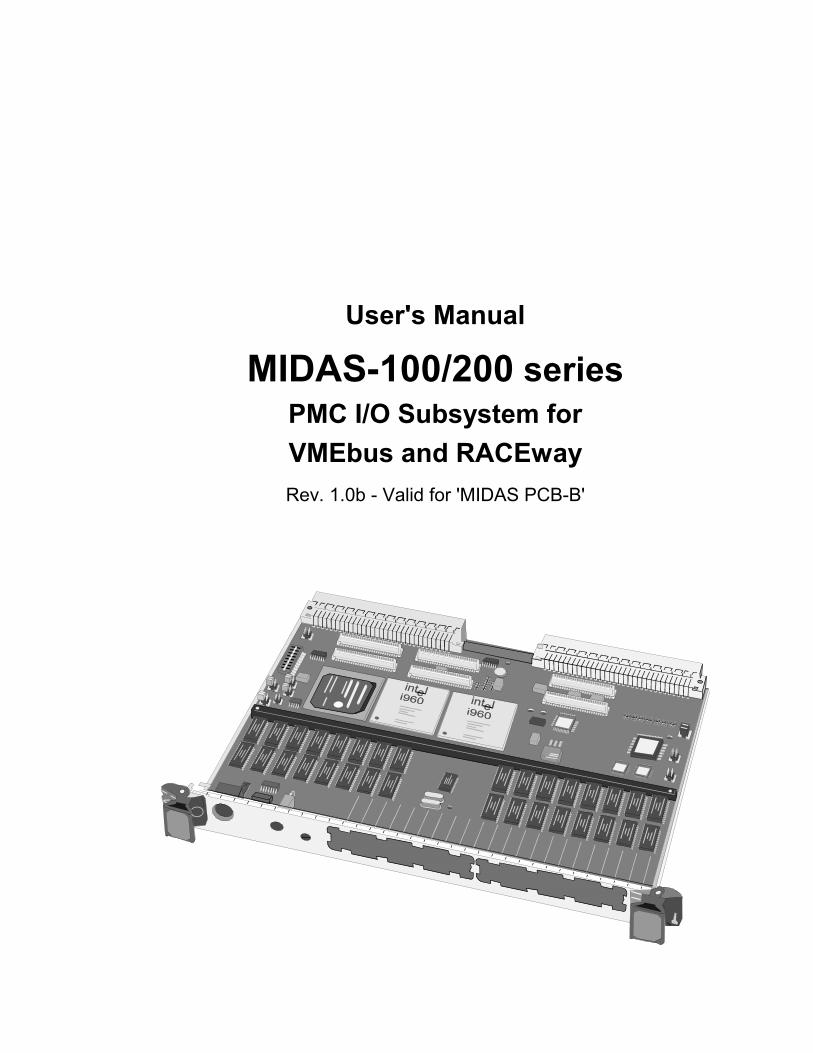
User's Manual
MIDAS-100/200 seriesPMC I/O Subsystem for
VMEbus and RACEway
Rev. 1.0b - Valid for 'MIDAS PCB-B'
MIDAS USER's MANUALii
The information in this document is subject to change without notice and should not beconstrued as a commitment by VMETRO. While reasonable precautions have been taken,
VMETRO assumes no responsibility for any errors that may appear in this document.
© Copyright VMETRO 2000.This document may not be furnished or disclosed to any third party
and may not be copied or reproduced in any form, electronic,mechanical, or otherwise, in whole or in part, without prior writtenconsent of VMETRO Inc. (Houston, TX, USA) or VMETRO A/S
(Oslo, Norway).

MIDAS USER's MANUAL iii
Warranty
VMETRO products are warranted against defective materials and workmanship within thewarranty period of 1 (one) year from date of invoice. Within the warranty period, VMETROwill, free of charge, repair or replace any defective unit covered by this warranty, shippingprepaid. A Return Authorization Code should be obtained from VMETRO prior to return ofany defective product. With any returned product, a written description of the nature ofmalfunction should be enclosed. The product must be shipped in its original shipping containeror similar packaging with sufficient mechanical and electrical protection in order to maintainwarranty.
This warranty assumes normal use. Products subjected to unreasonably rough handling,negligence, abnormal voltages, abrasion, unauthorized parts replacement and repairs, or theftare not covered by this warranty and will if possible be repaired for time and material chargesin effect at the time of repair.
VMETRO's warranty is limited to the repair or replacement policy described above and neitherVMETRO nor its agent shall be responsible for consequential or special damages related to theuse of their products.
Limited Liability
VMETRO does not assume any liability arising out of the application or use of any productdescribed herein; neither does it convey any license under its patent rights nor the rights ofothers. VMETRO products are not designed, intended, or authorized for use as components insystems intended to support or sustain life, or for any application in which failure of theVMETRO product could create a situation where personal injury or death may occur. ShouldBuyer purchase or use VMETRO products for any such unintended or unauthorizedapplication, Buyer shall indemnify and hold VMETRO and its officers, employees,subsidiaries, affiliates, and distributors harmless against all claims, costs, damages, andexpenses, and reasonable attorney fees arising out of, directly or indirectly, any claim ofpersonal injury or death associated with such unintended or unauthorized use, even if suchclaim alleges that VMETRO was negligent regarding the design or manufacture of the part.
USA: VMETRO, Inc.1880 Dairy Ashford, Suite 535 Houston, TX 77077, USATel.: (281) 584-0728Fax: (281) 584-9034Email: [email protected]
Europe, Asia: VMETRO asaBrynsveien 5N-0667 OSLO, NorwayTel.: +47 2210 6090Fax: +47 2210 6202Email: [email protected]
http://www.vmetro.com/

•••• Contents MIDAS USER's MANUALiv
MIDAS USER's MANUAL Contents •••• v
ContentsGeneral Information 1
This document ...........................................................................................................................1Conventions used in this document .............................................................................1Related Documents......................................................................................................2
Product Overview 3
MIDAS Family ..........................................................................................................................3The MIDAS-200 Series .............................................................................................................3
Twin i960RD I/O processors.......................................................................................3The MIDAS-100 Series .............................................................................................................4
i960RD I/O processor..................................................................................................4Main Components......................................................................................................................5
i960®RD I/O Processor ...............................................................................................5Universe II PCI-VMEbus Bridge ................................................................................6PXB PCI-RACEway Bridge........................................................................................7
Installation 7
Board Precautions......................................................................................................................7Unpacking..................................................................................................................................7Board Layout .............................................................................................................................8Installation of PMC Modules.....................................................................................................8Assembly Procedure for MIDAS-x50........................................................................................9Installation in VMEbus System ...............................................................................................12
Slot selection .............................................................................................................12Power consumption .................................................................................................................12Configuration Switch & Jumpers.............................................................................................13
Functional Description 14
i960®RD and its Surroundings.................................................................................................14i960®RD Address Map..............................................................................................15i960®RD Power-Up Options .....................................................................................15FLASH Memory........................................................................................................16RS232 Interface.........................................................................................................17Connecting two i960®RDs.........................................................................................17
VMEbus Interface (Universe II VME-PCI Bridge) .................................................................18'Universe II' Power-Up Options.................................................................................18Auto-Slot ID..............................................................................................................19Configuration ROM...................................................................................................19Switch & Jumper Descriptions ..................................................................................21Reset Button ..............................................................................................................24
RACEway Interface (PXB RACEway-PCI Bridge) ................................................................24Jumper Descriptions ..................................................................................................24
PCI Bus Details .......................................................................................................................25Arbitration .................................................................................................................25'IDSEL' Generation....................................................................................................27Subtractive Decoding Agent......................................................................................28
Interrupt Routing .....................................................................................................................29Interrupt Mode Selection...........................................................................................29Interrupt Jumpers.......................................................................................................30Interrupt Routing Tables ...........................................................................................30
•••• Contents MIDAS USER's MANUALvi
Interrupt Mode 0: ......................................................................................................31Interrupt Mode 1: ......................................................................................................32Interrupt Mode 2: ......................................................................................................33
Appendix I: PMC I/O Routing 35
PMC I/O Routing Scheme.......................................................................................................35
Appendix II: Universe II Configuration Examples 36
General Information ................................................................................................................36VMEbus Slave Images ............................................................................................................ 36
PCI Master Enable ....................................................................................................36VMEbus Register Access Image...............................................................................37VMEbus Slave Image 0 ............................................................................................38VMEbus Slave Image 1 ............................................................................................38VMEbus Slave Image 2 ............................................................................................39Initialization Sequence..............................................................................................39
PCI Slave Images ....................................................................................................................40PCI Target Enable - Memory & I/O Space ...............................................................40PCI Slave Image 0 ....................................................................................................41PCI Slave Image 1 ....................................................................................................42PCI Slave Image 2 ....................................................................................................42Initialization Sequence..............................................................................................43
Appendix III: PXB Information 44
PXB Register Descriptions......................................................................................................44P-Side Register Descriptions.....................................................................................44X-Side Register Descriptions....................................................................................51
Miscellaneous PXB Information .............................................................................................52Configuration Serial EEPROM.................................................................................52PCI-to-RACEway Addressing...................................................................................53RACEway-to-PCI Addressing...................................................................................55PCI-to-PCI Bridge Operation....................................................................................56
PXB Initialization Example.....................................................................................................57
Appendix IV: 61
List of Tables...........................................................................................................................61List of Figures .........................................................................................................................62
MIDAS USER's MANUAL General Information •••• 1
General InformationThis document
This document has been prepared to help the customer integrate MIDAS in theirVMEbus system. The following models are covered by this document:
MIDAS-120: Intelligent I/O Subsystem with single i960®RD and memory, andtwo PMC positions.
MIDAS-150: Intelligent I/O Subsystem with single i960®RD and memory, andfive PMC positions. Occupies two VMEbus slots.
MIDAS-220: Intelligent I/O Subsystem containing dual i960®RD withindependent memories, and two PMC positions.
MIDAS-250: Intelligent I/O Subsystem containing dual i960®RD withindependent memories, and five PMC positions. Occupies twoVMEbus slots.
The following options are described:
-R RACEway option. Interface to 160 MB/s RACEway crossbar.
-S Symmetrical configuration. Configuration option with one PMCposition on each PCI bus. Applies to MIDAS-120 and MIDAS-220 only.
Conventions used in this documentThe following section describes conventions used in this document.
Symbols Meaning:
The STOP symbol indicates a section of critical importance. Overlooking thisinformation may cause damage to the MIDAS and/or other equipment.
Indicates important, but not crucial, information. Still, you should take notice ifyou want to use all capabilities built into your MIDAS.
2 •••• General Information MIDAS USER's MANUAL
Related DocumentsThis document does not include detailed information about the following mainboard components:
• i960®RD Intelligent I/O Processor.
• 'Universe II' VME-to-PCI bridge chip.
• 'PXB' RACEway-to-PCI bridge chip.
Since a majority of the control registers, and a large part of the complexity of theMIDAS is implemented in these chips, their documentation contains information,which is essential to the understanding of the product.
VMEbus-PCI (Tundra): UNIVERSE II™ USER MANUAL
i960®RD (Intel Corp.): i960®RX I/O MICROPROCESSOR DEVELOPER’S MANUAL
i960®RD - DATA SHEET
RACEway-PCI PXB OVERVIEW
PXB BRIDGE SPECIFICATION
Documentation can be obtained from VMETRO by ordering a MIDAS Documentation Package.
The vendors of some of the major components used on MIDAS publish devicedata via Internet. Some components may contain design defects or errors known aserrata, which may cause the component to deviate from published specifications.The respective vendors, on their web pages document current characterized errata.
Vendor Component Available documentation
Tundra (formerly Newbridge) Universe II (VME-PCI Bridge) • User Manual
• Device Errata
• Application Notes
http://www.tundra.com/
Intel Corporation 80960RD (I/O Processor)
Not used on MIDAS-20/50
• User Manual
• Device Errata
• Application Notes
and more..
http://www.intel.com/design/i960/
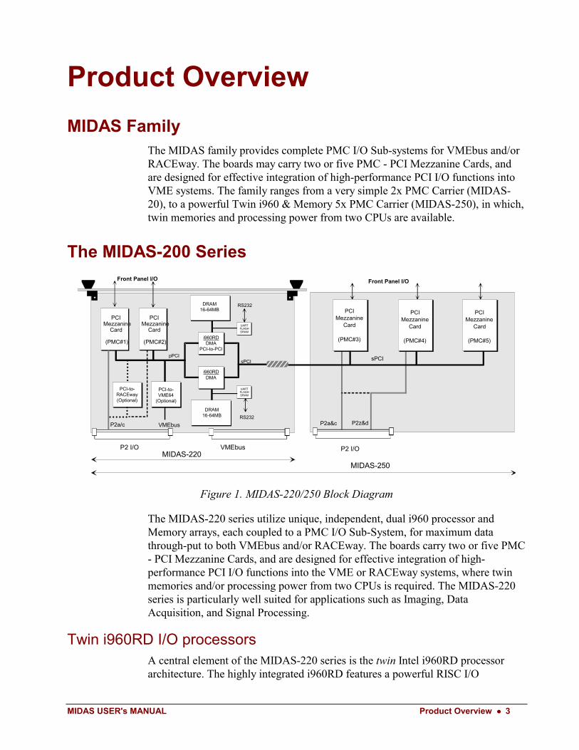
MIDAS USER's MANUAL Product Overview •••• 3
Product Overview
MIDAS FamilyThe MIDAS family provides complete PMC I/O Sub-systems for VMEbus and/orRACEway. The boards may carry two or five PMC - PCI Mezzanine Cards, andare designed for effective integration of high-performance PCI I/O functions intoVME systems. The family ranges from a very simple 2x PMC Carrier (MIDAS-20), to a powerful Twin i960 & Memory 5x PMC Carrier (MIDAS-250), in which,twin memories and processing power from two CPUs are available.
The MIDAS-200 Series
PCI-to-VME64
(Optional)
pPCI
i960RD DMA
PCI-to-PCI
VMEbusP2a/c
i960RD DMA
PCI-to-RACEway(Optional)
RS232
DRAM16-64MB
UARTFLASHSRAM
RS232
UARTFLASHSRAM
Front Panel I/O
PCIMezzanine
Card
(PMC#1)
PCIMezzanine
Card
(PMC#2)
PCIMezzanine
Card
(PMC#5)
sPCI
PCIMezzanine
Card
(PMC#3)
PCIMezzanine
Card
(PMC#4)
P2a&c P2z&d
Front Panel I/O
P2 I/O
sPCI
P2 I/O VMEbusMIDAS-220
MIDAS-250
DRAM16-64MB
Figure 1. MIDAS-220/250 Block Diagram
The MIDAS-220 series utilize unique, independent, dual i960 processor andMemory arrays, each coupled to a PMC I/O Sub-System, for maximum datathrough-put to both VMEbus and/or RACEway. The boards carry two or five PMC- PCI Mezzanine Cards, and are designed for effective integration of high-performance PCI I/O functions into the VME or RACEway systems, where twinmemories and/or processing power from two CPUs is required. The MIDAS-220series is particularly well suited for applications such as Imaging, DataAcquisition, and Signal Processing.
Twin i960RD I/O processors A central element of the MIDAS-220 series is the twin Intel i960RD processorarchitecture. The highly integrated i960RD features a powerful RISC I/O
4 •••• Product Overview MIDAS USER's MANUAL
processor, a PCI-to-PCI bridge, a memory controller and a flexible DMA-controller with linked-list capability.
Each of the two i960RDs has direct access to its own FLASH PROM, a RS232UART, all of the PCI resources on the board, and of course, its associated DRAMbank. This allows it to offload the host CPU by running dedicated I/O drivers forthe PMC modules mounted on the board.
For applications that do not need the processing power of the i960RD, but onlytwin DRAM memories and/or DMA, the processors may rest idle during normaloperation.
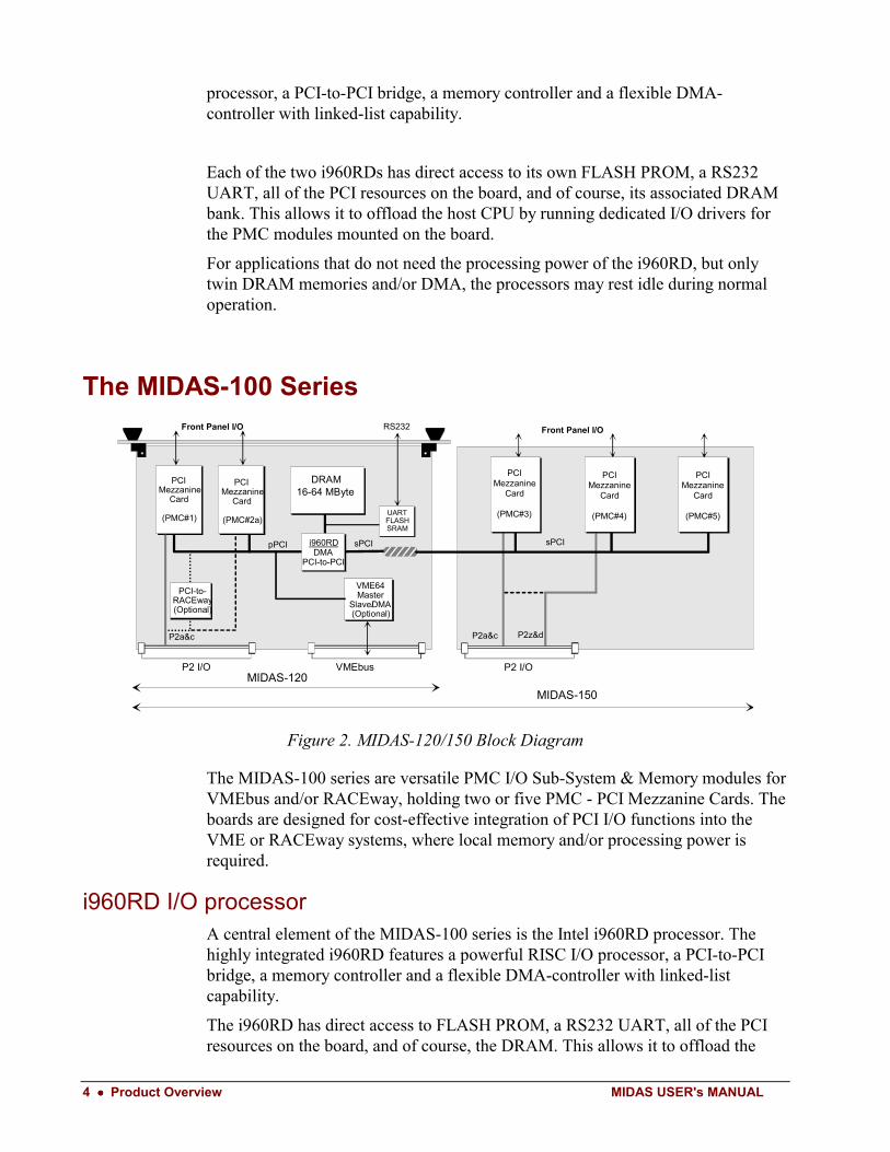
The MIDAS-100 Series
P2 I/O VMEbus
Front Panel I/O
VME64Master
Slave/DMA(Optional)
pPCI
PCIMezzanine
Card
(PMC#2a)
sPCI
PCIMezzanine
Card
(PMC#1)
DRAM16-64 MByte
i960RDDMA
PCI-to-PCI
RS232
UARTFLASHSRAM
MIDAS-120
MIDAS-150
PCIMezzanine
Card
(PMC#5)
sPCI
PCIMezzanine
Card
(PMC#3)
PCIMezzanine
Card
(PMC#4)
P2 I/O
P2a&c P2z&d
Front Panel I/O
PCI-to-RACEway(Optional)
P2a&c
Figure 2. MIDAS-120/150 Block Diagram
The MIDAS-100 series are versatile PMC I/O Sub-System & Memory modules forVMEbus and/or RACEway, holding two or five PMC - PCI Mezzanine Cards. Theboards are designed for cost-effective integration of PCI I/O functions into theVME or RACEway systems, where local memory and/or processing power isrequired.
i960RD I/O processorA central element of the MIDAS-100 series is the Intel i960RD processor. Thehighly integrated i960RD features a powerful RISC I/O processor, a PCI-to-PCIbridge, a memory controller and a flexible DMA-controller with linked-listcapability.
The i960RD has direct access to FLASH PROM, a RS232 UART, all of the PCIresources on the board, and of course, the DRAM. This allows it to offload the
MIDAS USER's MANUAL Product Overview •••• 5
host CPU by running dedicated I/O drivers for the PMC modules mounted on theboard.
Main Components
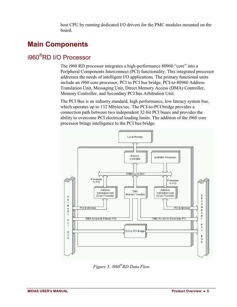
i960®RD I/O ProcessorThe i960 RD processor integrates a high-performance 80960 “core” into aPeripheral Components Interconnect (PCI) functionality. This integrated processoraddresses the needs of intelligent I/O applications. The primary functional unitsinclude an i960 core processor, PCI to PCI bus bridge, PCI-to-80960 AddressTranslation Unit, Messaging Unit, Direct Memory Access (DMA) Controller,Memory Controller, and Secondary PCI bus Arbitration Unit.
The PCI Bus is an industry standard, high performance, low latency system bus,which operates up to 132 Mbytes/sec. The PCI-to-PCI bridge provides aconnection path between two independent 32-bit PCI buses and provides theability to overcome PCI electrical loading limits. The addition of the i960 coreprocessor brings intelligence to the PCI bus bridge.
Figure 3. i960®RD Data Flow
6 •••• Product Overview MIDAS USER's MANUAL
The i960 RD processor is a multi-function PCI device: Function 0 is the PCI-to-PCI bridge, Function 1 is the Address Translation Unit. The i960 RD processorcontains PCI configuration space, which is accessible through the primary PCI bus.This multi-function PCI device is fully compliant with the PCI Local BusSpecification Revision 2.1.
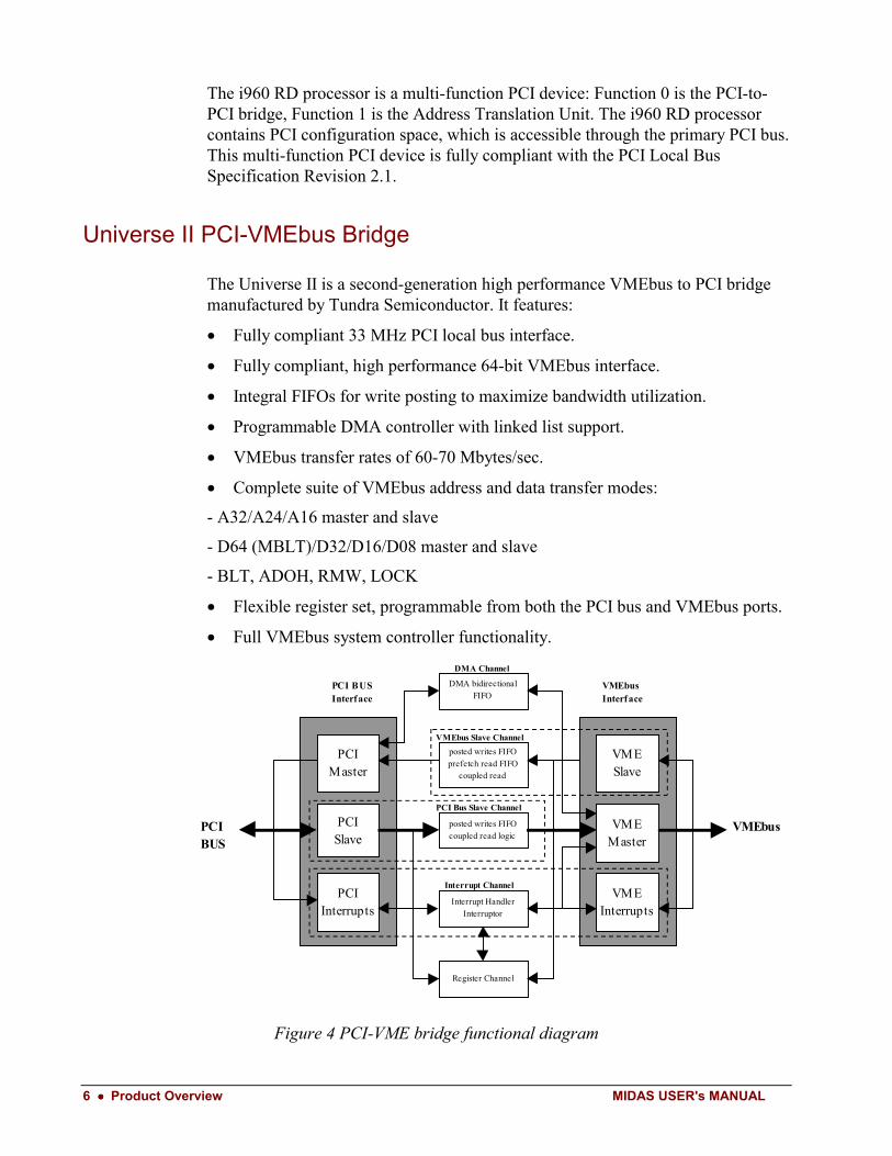
Universe II PCI-VMEbus Bridge
The Universe II is a second-generation high performance VMEbus to PCI bridgemanufactured by Tundra Semiconductor. It features:
• Fully compliant 33 MHz PCI local bus interface.
• Fully compliant, high performance 64-bit VMEbus interface.
• Integral FIFOs for write posting to maximize bandwidth utilization.
• Programmable DMA controller with linked list support.
• VMEbus transfer rates of 60-70 Mbytes/sec.
• Complete suite of VMEbus address and data transfer modes:
- A32/A24/A16 master and slave
- D64 (MBLT)/D32/D16/D08 master and slave
- BLT, ADOH, RMW, LOCK
• Flexible register set, programmable from both the PCI bus and VMEbus ports.
• Full VMEbus system controller functionality.
Register Channel
Interrupt Handler
Interruptor
posted writes FIFO
coupled read logic
posted writes FIFO
prefetch read FIFO coupled read
DMA bidirectional
FIFO
PCIInterrupts
PCISlave
PCIMaster
VMESlave
VMEMaster
VMEInterrupts
PCIBUS
VMEbus
PCI BUSInterface
VMEbusInterface
VMEbus Slave Channel
PCI Bus Slave Channel
Interrupt Channel
DMA Channel
Figure 4 PCI-VME bridge functional diagram
MIDAS USER's MANUAL Installation •••• 7
PXB PCI-RACEway Bridge
The PXB is a high performance RACEway to PCI bridge developed by MercuryComputer Systems. It features:
• Bridges a 32 bit, 33MHz PCI bus with a 32 bit, 40MHz RACEway switchingfabric.
• Compliant to Rev 2.1 PCI local bus specification, including delayedoperations.
• Compliant to Rev 1.0 PCI to PCI Bridge specification.
• Bridges up to sixteen 32 bit, 33MHz PCI busses
• Able to sustain up to 125MB/sec with large memory write transfers, and100MB/sec with large memory read transfers.
• Integral FIFOs for write posting to maximize bandwidth utilization.
Installation
Board Precautions
The MIDAS circuit board is sensitive to static electricity and can be damaged by astatic discharge. Always wear a grounded anti-static wrist strap and use grounded,static protected work surfaces when touching the circuit board and its components.
When the board is not installed, always keep in the static-protective envelope.
UnpackingAll precautions described above must be taken when unpacking the MIDAS fromits shipping container. Verify that no damage has occurred in the shipment. Referto packing list and verify that all items are present.
8 •••• Installation MIDAS USER's MANUAL
Board Layout
i960RD#2
i960RD#1
UNIVERSE
VME-TO-PCI
PXB
JP1
JP2
JP4
JP5 JP
14
JP7
JP9
JP15
JP3
JP6
JP10
JP13
JP11
SW1
RST DISBASE ADDR
BO
OT
SFA
IL
AU
TO
ID
VRAI
FLA
SH
RA
CE
way
INT
ASIZE
��������������������������������������������������������������������������������������������������������������������������������������������������������������������������������������������������������������������������������������������������������������������������������������������������������������������������������������������������������������������������������������������������������������������������������������������������������������������������������������������������������������������������������������������������������������������������������������������������������������������������������������������������������������������������������������������������������������������������������������������������������������������������������������������������������������������������������������������
PMC #2
PMC #1
P2 I/O CONNECTOR – PMC#2a(Not mounted for –S or –R options)
RESET SWITCH(-S OPTION)
PCI CONNECTOR PMC#2b&MIDAS-x50 Expansion
PCI CONNECTOR PMC#2a(Not mounted for –S option)
RS232 CONNECTOR
RESET BUTTON
VME-to-PCI BRIDGE
PCI CONNECTORSPMC#1
P2 I/O CONNECTOR(Not -R option)
INTERRUPTJUMPERS
RACEwayJUMPERS
FLASHJUMPERS
VMEbus CONFIGURATIONJUMPERS & SWITCH
BOOT MODESELECTION
Figure 5. MIDAS Board Layout (No model has all parts mounted.)
Installation of PMC ModulesThe MIDAS is shipped with two PMC filler panels mounted in the front panel.They act as EMC shielding in unused PMC positions. Before installing a PMCmodule, the filler panel(s) must be removed. This is done by pushing them outfrom the backside of the front panel.
Four screws must be used to secure each PMC on the MIDAS board.
MIDAS USER's MANUAL Installation •••• 9
Note: Be extremely careful when inserting screws to secure PMC modules.Touching component leads, or the printed circuit board itself, with a screwdrivermay cause permanent damage to the board
Assembly Procedure for MIDAS-x50The MIDAS-x50 is a dual slot VMEbus board that mates the back-planeconnectors in two neighbor slots. The MIDAS-x50 module can handle the insertionand extraction forces applied when installing or removing it from the backplane.However, this requires that the assembly procedure described in this section befollowed.
WARNING: The MIDAS-x50 boards may be destroyed during insertion orextraction from a VMEbus system if this procedure is not followed.
STEP#1: Dismount MEZZ-x50 board from MIDAS-x20 board.
- Place the MIDAS-x50 board on a smooth static protected work surface with thebottom side of the MIDAS-x20 board facing up.
- From the bottom side of the MIDAS-x20 PCB, remove the 5 screws holding themetal spacers between the MEZZ-x50 and MIDAS-x20. (these screws are locatedclose to the edge of the board in each corner, and between the VMEbusconnectors). Note: Do not throw away the screws. They are needed later in thisprocedure.
- Pull the boards carefully apart. Use hand force only, applied to the two upperVMEbus connectors for both boards.
- If the small SPACER-x50 PCB is attached to the MIDAS-x20 PCB after theseparation, remove it and mount it on the bottom side of the MEZZ-x50 boardinstead.
STEP#2: Mount PMC modules 1 and 2 on the MIDAS-x20 board.
- Place the MIDAS-x20 board on a smooth static protected work surface.
- Install PMC module #1 in the lower PMC position
- Install PMC module #2 in the upper PMC position
- Secure PMC modules with screws on the bottom side of the MIDAS-x20 board.
10 •••• Installation MIDAS USER's MANUAL
STEP#3: Mount PMC modules 3, 4 and 5 on the MEZZ-x50 board.
- Place the MEZZ-x50 board on a smooth static protected work surface.
- Install PMC module #3 in the lower PMC position.
- Install PMC module #4 in the middle PMC position.
- Install PMC module #5 in the upper PMC position.
- Secure the PMC modules with screws on the bottom side of the MEZZ-x50board.
MEZZ-x50 PCB-A
J31 J32
J34
J41 J42
J44
J51 J52
J11 J12
J14
J21 J22
J24
MIDAS-20 PMC Carrier for VMEbus
MIDAS-20 PCB-B
J51 J52
J50
DECchip 21052
PMC MODULE #5
PMC MODULE #3
PMC MODULE #4
PMC MODULE #1
PMC MODULE #2
Figure 6. Steps 2&3: Mount PMC modules on the MEZZ-x50 and MIDAS-x20 boards.
Note: Before proceeding, make sure the switch and jumper settings of theMIDAS-x20 board are set according to the needs of your application.
MIDAS USER's MANUAL Installation •••• 11
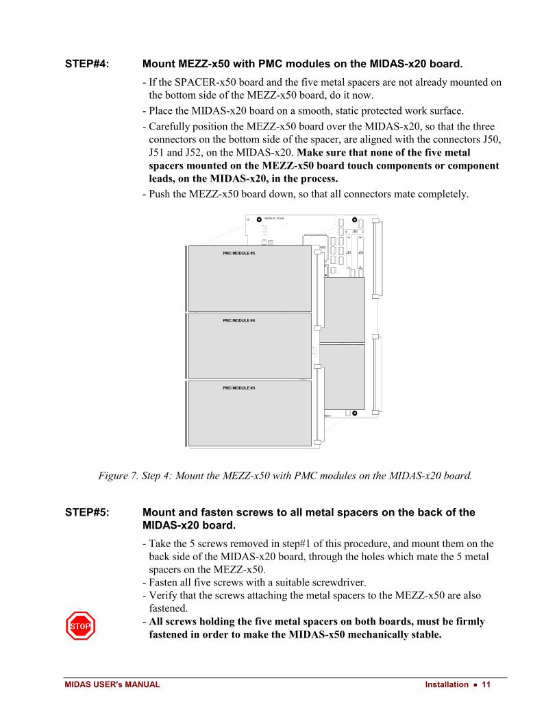
STEP#4: Mount MEZZ-x50 with PMC modules on the MIDAS-x20 board.
- If the SPACER-x50 board and the five metal spacers are not already mounted onthe bottom side of the MEZZ-x50 board, do it now.
- Place the MIDAS-x20 board on a smooth, static protected work surface.
- Carefully position the MEZZ-x50 board over the MIDAS-x20, so that the threeconnectors on the bottom side of the spacer, are aligned with the connectors J50,J51 and J52, on the MIDAS-x20. Make sure that none of the five metalspacers mounted on the MEZZ-x50 board touch components or componentleads, on the MIDAS-x20, in the process.
- Push the MEZZ-x50 board down, so that all connectors mate completely.
J11 J12
J14
J21 J22
J24
MIDAS-20 PMC Carrier for VMEbus
MIDAS-20 PCB-B
J51 J52
J50
DECchip 21052
PMC MODULE #1
PMC MODULE #2
MEZZ-x50 PCB-A
J31 J32
J34
J41 J42
J44
J51 J52
PMC MODULE #5
PMC MODULE #3
PMC MODULE #4
Figure 7. Step 4: Mount the MEZZ-x50 with PMC modules on the MIDAS-x20 board.
STEP#5: Mount and fasten screws to all metal spacers on the back of theMIDAS-x20 board.
- Take the 5 screws removed in step#1 of this procedure, and mount them on theback side of the MIDAS-x20 board, through the holes which mate the 5 metalspacers on the MEZZ-x50.
- Fasten all five screws with a suitable screwdriver.- Verify that the screws attaching the metal spacers to the MEZZ-x50 are also
fastened.- All screws holding the five metal spacers on both boards, must be firmly
fastened in order to make the MIDAS-x50 mechanically stable.

12 •••• Installation MIDAS USER's MANUAL
Installation in VMEbus System
Slot selectionThe MIDAS can be installed in any slot in a 6U VMEbus chassis, as long as thedaisy-chains for the bus grant and interrupt acknowledge signals arecontinuous from slot#1 to the slot in which the MIDAS is installed.
Installation into slot#1 of a VMEbus system is automatically detected, as specifiedin the VME64 specification. System controller functions are also enabled as aconsequence.
WARNING: Do not install the board in a powered system!
Power consumption
WARNING: Due to its power consumption, the MIDAS board requires forcedair cooling for reliable operation. Operation on extender boards is notrecommended.
Model Memory Size Operating Mode Power Consumptiontyp. @ +5V
MIDAS-220Y/M 32MB Both processors are in the idle state. 14.5WMIDAS-220 Y/M 32MB One processor transferring data
across VME and Raceway, theother processor idle
14.7W
MIDAS-220 Y/M 32MB One processor transferring dataacross VME and Raceway, theother processor performing anextended selftest
15.2W
MIDAS-220 SR 128MB Both processors are in the idle state. 15.0WMIDAS-220 SR 128MB One processor transferring data
across VME and Raceway, theother processor idle
15.7W
MIDAS-220 SR 128MB One processor transferring dataacross VME and Raceway, theother processor performing anextended selftest
17.0W
MIDAS-120 32MB Processor Idle 10.5WMIDAS-120 32MB Processor running selftest 11.5WMIDAS-120 32MB Processor transferring data over
VME11.5W
Table 1. Power Consumption
MIDAS USER's MANUAL Installation •••• 13
Configuration Switch & JumpersThe MIDAS has a large number of configuration registers, which need to beinitialized before the board is operational. Most registers are normally initializedby an i960®RD, but in some applications, an external host processor can performthis initialization, or parts of it, over VMEbus or RACEway. To allow this, powerup options in some MIDAS components are loaded from jumpers or a DIPswitch.
A detailed description of each jumper is included in the relevant part of the“Functional Description” section.
14 •••• Functional Description MIDAS USER's MANUAL
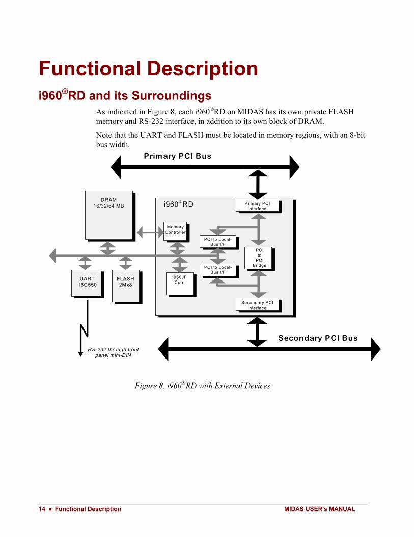
Functional Descriptioni960®RD and its Surroundings
As indicated in Figure 8, each i960®RD on MIDAS has its own private FLASHmemory and RS-232 interface, in addition to its own block of DRAM.
Note that the UART and FLASH must be located in memory regions, with an 8-bitbus width.
Primary PCI Bus
PCI to Local-Bus I/F
i960JFCore
PCIto
PCIBridgePCI to Local-
Bus I/F
MemoryController
i960®RDDRAM
16/32/64 MB
Secondary PCI Bus
Secondary PCIInterface
Primary PCIInterface
RS-232 through frontpanel mini-DIN
UART16C550
FLASH2Mx8
Figure 8. i960®RD with External Devices
MIDAS USER's MANUAL Functional Description •••• 15
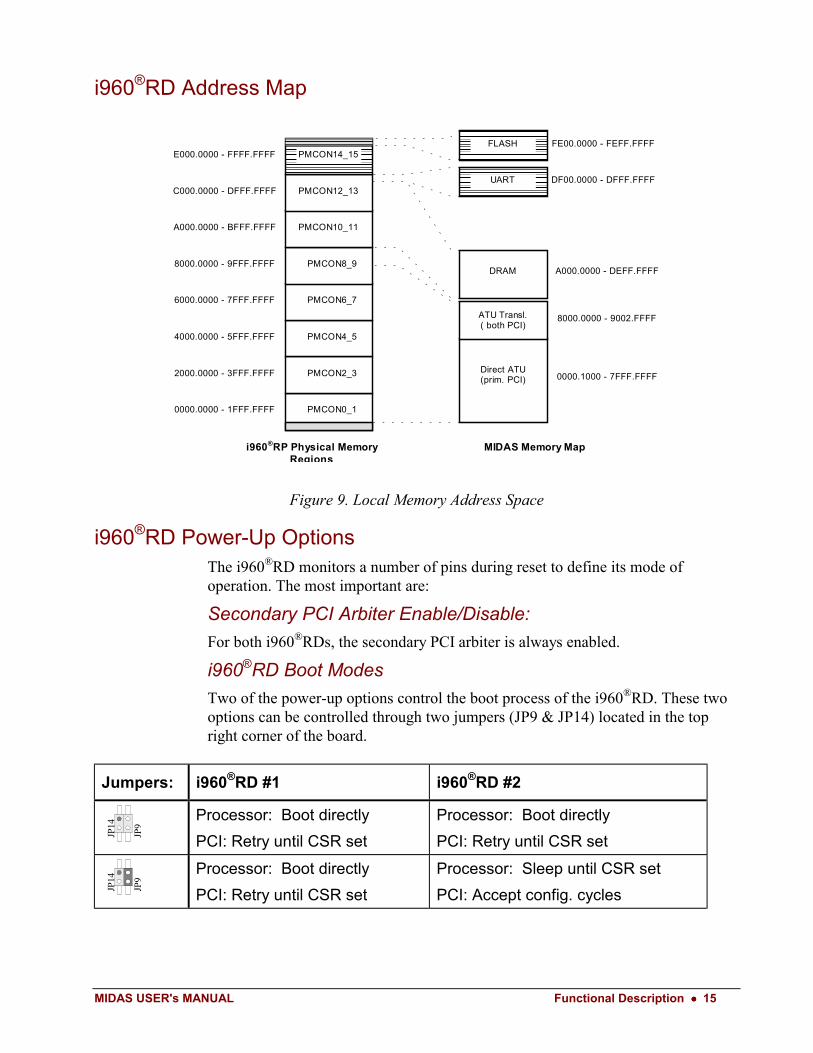
i960®RD Address Map
0000.0000 - 1FFF.FFFF
i960®RP Physical MemoryRegions
MIDAS Memory Map
PMCON0_1
2000.0000 - 3FFF.FFFF PMCON2_3
4000.0000 - 5FFF.FFFF PMCON4_5
6000.0000 - 7FFF.FFFF PMCON6_7
8000.0000 - 9FFF.FFFF PMCON8_9
A000.0000 - BFFF.FFFF PMCON10_11
C000.0000 - DFFF.FFFF PMCON12_13
8000.0000 - 9002.FFFF
0000.1000 - 7FFF.FFFF
DF00.0000 - DFFF.FFFF
E000.0000 - FFFF.FFFFFE00.0000 - FEFF.FFFF
���������������������������������������������������������������������������������������������������������������������PMCON14_15
���������������������������������������
Direct ATU(prim. PCI)
���������������������������������������������������������������������������������������������������������������������FLASH
���������������������������������������������������������������������������������������������������������������������
ATU Transl.( both PCI)
A000.0000 - DEFF.FFFFDRAM
UART
Figure 9. Local Memory Address Space
i960®RD Power-Up OptionsThe i960®RD monitors a number of pins during reset to define its mode ofoperation. The most important are:
Secondary PCI Arbiter Enable/Disable:
For both i960®RDs, the secondary PCI arbiter is always enabled.
i960®RD Boot Modes
Two of the power-up options control the boot process of the i960®RD. These twooptions can be controlled through two jumpers (JP9 & JP14) located in the topright corner of the board.
Jumpers: i960®RD #1 i960®RD #2
JP14
JP9
Processor: Boot directly
PCI: Retry until CSR set
Processor: Boot directly
PCI: Retry until CSR set
JP14
JP9
Processor: Boot directly
PCI: Retry until CSR set
Processor: Sleep until CSR set
PCI: Accept config. cycles
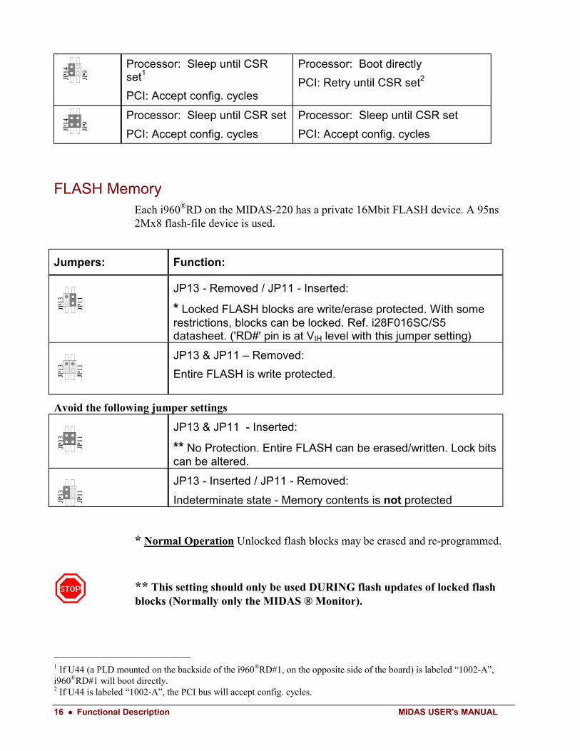
16 •••• Functional Description MIDAS USER's MANUAL
JP14
JP9
Processor: Sleep until CSRset1
PCI: Accept config. cycles
Processor: Boot directly
PCI: Retry until CSR set2JP
14
JP9
Processor: Sleep until CSR set
PCI: Accept config. cycles
Processor: Sleep until CSR set
PCI: Accept config. cycles
FLASH MemoryEach i960®RD on the MIDAS-220 has a private 16Mbit FLASH device. A 95ns2Mx8 flash-file device is used.
Jumpers: Function:
JP13
JP11
JP13 - Removed / JP11 - Inserted:
* Locked FLASH blocks are write/erase protected. With somerestrictions, blocks can be locked. Ref. i28F016SC/S5datasheet. ('RD#' pin is at VIH level with this jumper setting)
JP13
JP11
JP13 & JP11 – Removed:
Entire FLASH is write protected.
Avoid the following jumper settings
JP13
JP11
JP13 & JP11 - Inserted:
** No Protection. Entire FLASH can be erased/written. Lock bitscan be altered.
JP13
JP11
JP13 - Inserted / JP11 - Removed:
Indeterminate state - Memory contents is not protected
* Normal Operation Unlocked flash blocks may be erased and re-programmed.
** This setting should only be used DURING flash updates of locked flashblocks (Normally only the MIDAS ® Monitor).
1 If U44 (a PLD mounted on the backside of the i960®RD#1, on the opposite side of the board) is labeled “1002-A”,i960®RD#1 will boot directly.2 If U44 is labeled “1002-A”, the PCI bus will accept config. cycles.
MIDAS USER's MANUAL Functional Description •••• 17
FE08.0000 - FEFF.FFFF
FE00.0000 - FE07.FFFF FLASH
FLASHShadow
FEFF.FF30 Boot Record
Figure 10. FLASH Boot Address
RS232 InterfaceEach i960®RD on the MIDAS-220 has a private UART for serial portcommunication. The 'TL16C550' is used for this purpose.
Both RS-232 interfaces share a mini-DIN connector for connection through thefront panel.
The UART is located at a fixed address in the i960 address space. The baseaddress is 0xDF00.0000. The eight most significant address bits are used for theaddress decoding, which means that a 16MB window is occupied.
RS232 Cables
MIDAS-100 and MIDAS-200 series boards are shipped with a short convertercable to allow standard D-SUB cables to connect to the non-standard, Mini-DINMIDAS connector.
The cable for the MIDAS-200 board is a split cable, with one 9 pin D-subconnector for each processor. The shorter cable connects to the UART ofi960®RD#1, while the longer cable connects to processor number two.
12
4 356
789 PIN 1: TxD1PIN 2: TxD2PIN 3: RxD1PIN 4: RxD2PIN 5: GND
Figure 11. Pin definition for the RS232 female connector mounted on the frontpanel
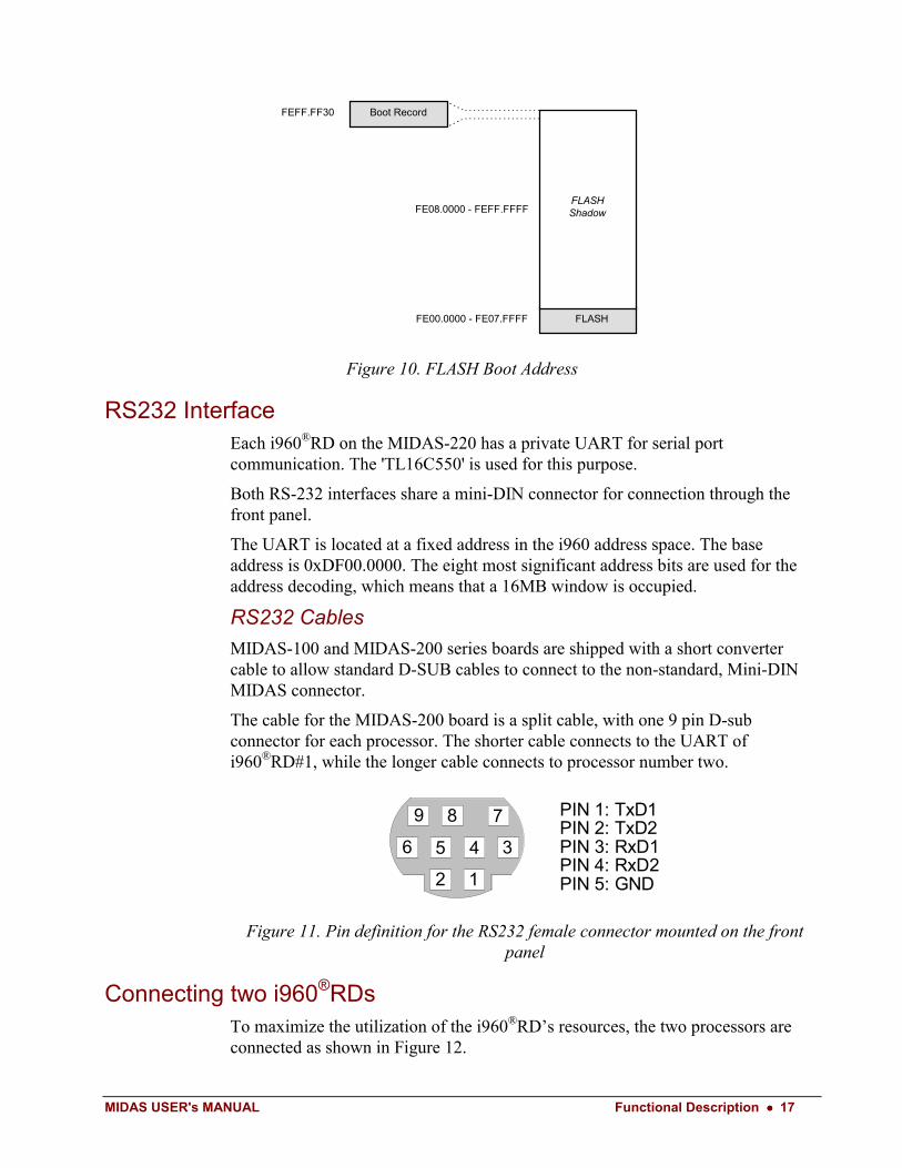
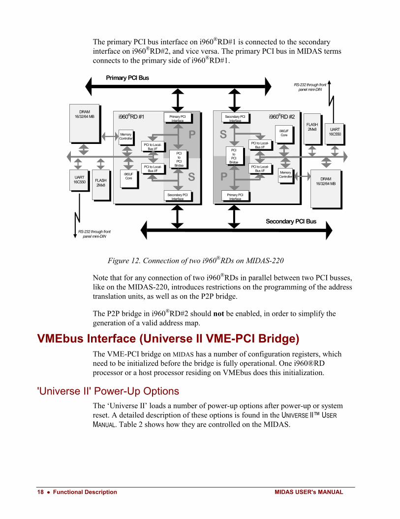
Connecting two i960®RDsTo maximize the utilization of the i960®RD’s resources, the two processors areconnected as shown in Figure 12.
18 •••• Functional Description MIDAS USER's MANUAL
The primary PCI bus interface on i960®RD#1 is connected to the secondaryinterface on i960®RD#2, and vice versa. The primary PCI bus in MIDAS termsconnects to the primary side of i960®RD#1.
PCI to Local-Bus I/F
i960JFCore
PCIto
PCIBridge
PCI to Local-Bus I/F
MemoryController
Primary PCI Bus
i960®RD #2
PCI to Local-Bus I/F
i960JFCore
PCIto
PCIBridgePCI to Local-
Bus I/F
MemoryController
i960®RD #1
Secondary PCI Bus
P
SSecondary PCI
Interface
Primary PCIInterface
Secondary PCIInterface
Primary PCIInterface
P
S
DRAM16/32/64 MB
RS-232 through frontpanel mini-DIN
FLASH2Mx8
UART16C550
DRAM16/32/64 MB
RS-232 through frontpanel mini-DIN
UART16C550
FLASH2Mx8
Figure 12. Connection of two i960®RDs on MIDAS-220
Note that for any connection of two i960®RDs in parallel between two PCI busses,like on the MIDAS-220, introduces restrictions on the programming of the addresstranslation units, as well as on the P2P bridge.
The P2P bridge in i960®RD#2 should not be enabled, in order to simplify thegeneration of a valid address map.
VMEbus Interface (Universe II VME-PCI Bridge)The VME-PCI bridge on MIDAS has a number of configuration registers, whichneed to be initialized before the bridge is fully operational. One i960®RDprocessor or a host processor residing on VMEbus does this initialization.
'Universe II' Power-Up OptionsThe ‘Universe II’ loads a number of power-up options after power-up or systemreset. A detailed description of these options is found in the UNIVERSE II™ USERMANUAL. Table 2 shows how they are controlled on the MIDAS.
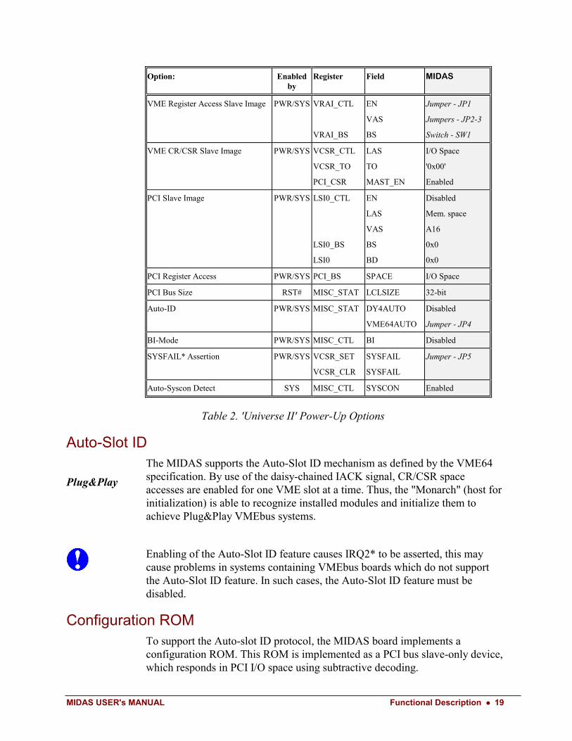
MIDAS USER's MANUAL Functional Description •••• 19
Option: Enabledby
Register Field MIDAS
VME Register Access Slave Image PWR/SYS VRAI_CTL
VRAI_BS
EN
VAS
BS
Jumper - JP1
Jumpers - JP2-3
Switch - SW1
VME CR/CSR Slave Image PWR/SYS VCSR_CTL
VCSR_TO
PCI_CSR
LAS
TO
MAST_EN
I/O Space
'0x00'
Enabled
PCI Slave Image PWR/SYS LSI0_CTL
LSI0_BS
LSI0
EN
LAS
VAS
BS
BD
Disabled
Mem. space
A16
0x0
0x0
PCI Register Access PWR/SYS PCI_BS SPACE I/O Space
PCI Bus Size RST# MISC_STAT LCLSIZE 32-bit
Auto-ID PWR/SYS MISC_STAT DY4AUTO
VME64AUTO
Disabled
Jumper - JP4
BI-Mode PWR/SYS MISC_CTL BI Disabled
SYSFAIL* Assertion PWR/SYS VCSR_SET
VCSR_CLR
SYSFAIL
SYSFAIL
Jumper - JP5
Auto-Syscon Detect SYS MISC_CTL SYSCON Enabled
Table 2. 'Universe II' Power-Up Options
Auto-Slot ID
Plug&Play
The MIDAS supports the Auto-Slot ID mechanism as defined by the VME64specification. By use of the daisy-chained IACK signal, CR/CSR spaceaccesses are enabled for one VME slot at a time. Thus, the "Monarch" (host forinitialization) is able to recognize installed modules and initialize them toachieve Plug&Play VMEbus systems.
Enabling of the Auto-Slot ID feature causes IRQ2* to be asserted, this maycause problems in systems containing VMEbus boards which do not supportthe Auto-Slot ID feature. In such cases, the Auto-Slot ID feature must bedisabled.
Configuration ROMTo support the Auto-slot ID protocol, the MIDAS board implements aconfiguration ROM. This ROM is implemented as a PCI bus slave-only device,which responds in PCI I/O space using subtractive decoding.
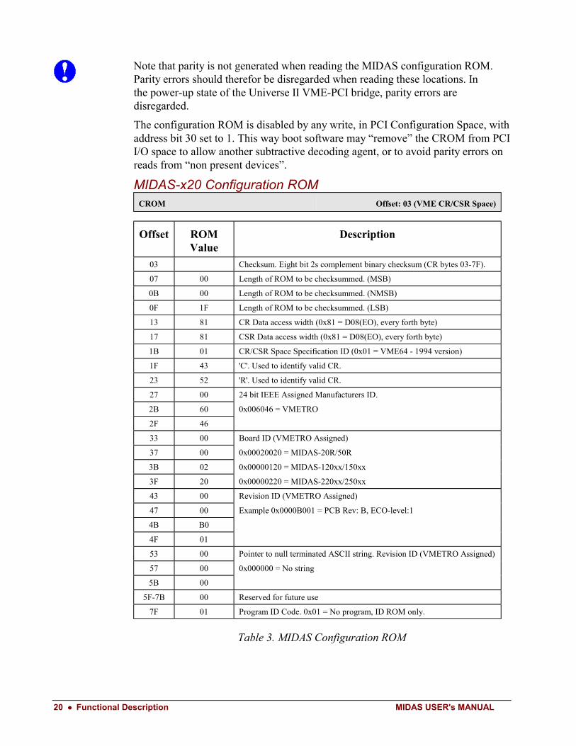
20 •••• Functional Description MIDAS USER's MANUAL
Note that parity is not generated when reading the MIDAS configuration ROM.Parity errors should therefor be disregarded when reading these locations. Inthe power-up state of the Universe II VME-PCI bridge, parity errors aredisregarded.
The configuration ROM is disabled by any write, in PCI Configuration Space, withaddress bit 30 set to 1. This way boot software may “remove” the CROM from PCII/O space to allow another subtractive decoding agent, or to avoid parity errors onreads from “non present devices”.
MIDAS-x20 Configuration ROMCROM Offset: 03 (VME CR/CSR Space)
Offset ROMValue
Description
03 Checksum. Eight bit 2s complement binary checksum (CR bytes 03-7F).
07 00 Length of ROM to be checksummed. (MSB)
0B 00 Length of ROM to be checksummed. (NMSB)
0F 1F Length of ROM to be checksummed. (LSB)
13 81 CR Data access width (0x81 = D08(EO), every forth byte)
17 81 CSR Data access width (0x81 = D08(EO), every forth byte)
1B 01 CR/CSR Space Specification ID (0x01 = VME64 - 1994 version)
1F 43 'C'. Used to identify valid CR.
23 52 'R'. Used to identify valid CR.
27 00 24 bit IEEE Assigned Manufacturers ID.
2B 60 0x006046 = VMETRO
2F 46
33 00 Board ID (VMETRO Assigned)
37 00 0x00020020 = MIDAS-20R/50R
3B 02 0x00000120 = MIDAS-120xx/150xx
3F 20 0x00000220 = MIDAS-220xx/250xx
43 00 Revision ID (VMETRO Assigned)
47 00 Example 0x0000B001 = PCB Rev: B, ECO-level:1
4B B0
4F 01
53 00 Pointer to null terminated ASCII string. Revision ID (VMETRO Assigned)
57 00 0x000000 = No string
5B 00
5F-7B 00 Reserved for future use
7F 01 Program ID Code. 0x01 = No program, ID ROM only.
Table 3. MIDAS Configuration ROM
MIDAS USER's MANUAL Functional Description •••• 21
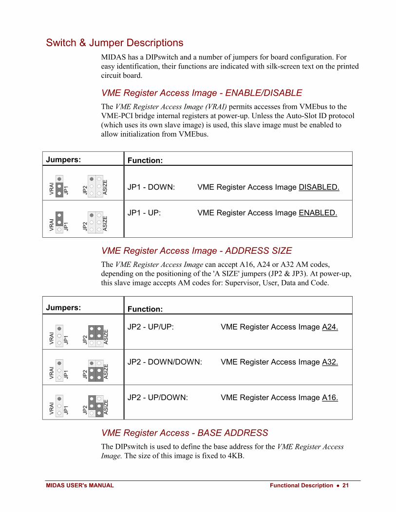
Switch & Jumper DescriptionsMIDAS has a DIPswitch and a number of jumpers for board configuration. Foreasy identification, their functions are indicated with silk-screen text on the printedcircuit board.
VME Register Access Image - ENABLE/DISABLE
The VME Register Access Image (VRAI) permits accesses from VMEbus to theVME-PCI bridge internal registers at power-up. Unless the Auto-Slot ID protocol(which uses its own slave image) is used, this slave image must be enabled toallow initialization from VMEbus.
Jumpers: Function:
VR
AI
JP1
JP2
AS
IZE
JP1 - DOWN: VME Register Access Image DISABLED.
VR
AI
JP1
JP2
AS
IZE
JP1 - UP: VME Register Access Image ENABLED.
VME Register Access Image - ADDRESS SIZE
The VME Register Access Image can accept A16, A24 or A32 AM codes,depending on the positioning of the 'A SIZE' jumpers (JP2 & JP3). At power-up,this slave image accepts AM codes for: Supervisor, User, Data and Code.
Jumpers: Function:
VR
AI
JP1
JP2
AS
IZE
JP2 - UP/UP: VME Register Access Image A24.
VR
AI
JP1
JP2
AS
IZE JP2 - DOWN/DOWN: VME Register Access Image A32.
VR
AI
JP1
JP2
AS
IZE JP2 - UP/DOWN: VME Register Access Image A16.
VME Register Access - BASE ADDRESS
The DIPswitch is used to define the base address for the VME Register AccessImage. The size of this image is fixed to 4KB.
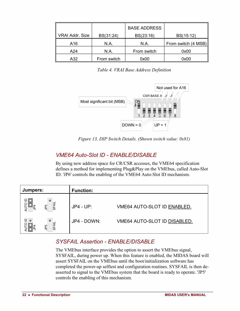
22 •••• Functional Description MIDAS USER's MANUAL
VRAI Addr. Size BS[31:24]
BASE ADDRESS
BS[23:16] BS[15:12]
A16 N.A. N.A. From switch (4 MSB)
A24 N.A. From switch 0x00
A32 From switch 0x00 0x00
Table 4. VRAI Base Address Definition
CSR BASE ADDRESS
ON
1 2 3 4 5 6 7 8
Most significant bit (MSB)
DOWN = 0 UP = 1
Not used for A16
Figure 13. DIP Switch Details. (Shown switch value: 0x81)
VME64 Auto-Slot ID - ENABLE/DISABLE
By using new address space for CR/CSR accesses, the VME64 specificationdefines a method for implementing Plug&Play on the VMEbus, called Auto-SlotID. 'JP6' controls the enabling of the VME64 Auto-Slot ID mechanism.
Jumpers: Function:
AU
TO
ID
JP4
JP5
SF
AIL
JP4 - UP: VME64 AUTO-SLOT ID ENABLED.
AU
TO
ID
JP4
JP5
SF
AIL JP4 - DOWN: VME64 AUTO-SLOT ID DISABLED.
SYSFAIL Assertion - ENABLE/DISABLE
The VMEbus interface provides the option to assert the VMEbus signal,SYSFAIL, during power up. When this feature is enabled, the MIDAS board willassert SYSFAIL on the VMEbus until the boot/initialization software hascompleted the power-up selftest and configuration routines. SYSFAIL is then de-asserted to signal to the VMEbus system that the board is ready to operate. 'JP5'controls the enabling of this mechanism.
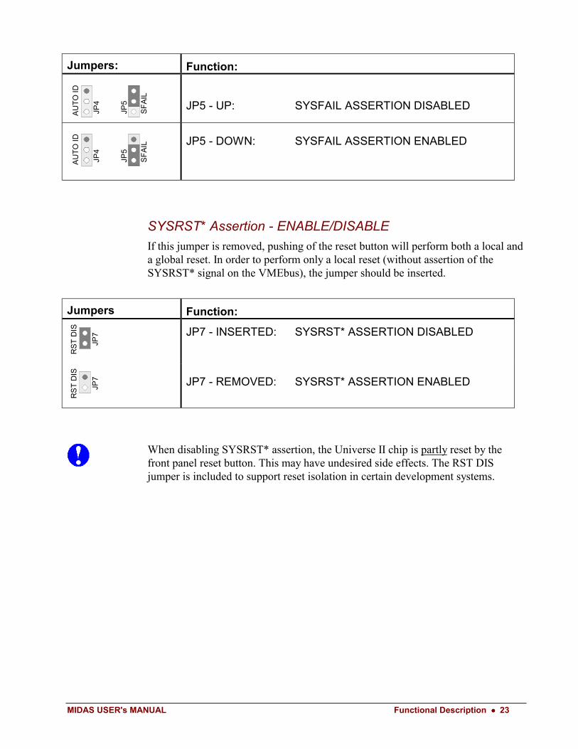
MIDAS USER's MANUAL Functional Description •••• 23
Jumpers: Function:
AU
TO
ID
JP4
JP5
SF
AIL
JP5 - UP: SYSFAIL ASSERTION DISABLED
AU
TO
ID
JP4
JP5
SF
AIL
JP5 - DOWN: SYSFAIL ASSERTION ENABLED
SYSRST* Assertion - ENABLE/DISABLE
If this jumper is removed, pushing of the reset button will perform both a local anda global reset. In order to perform only a local reset (without assertion of theSYSRST* signal on the VMEbus), the jumper should be inserted.
Jumpers Function:
JP7
RS
T D
IS
JP7 - INSERTED: SYSRST* ASSERTION DISABLED
JP7
RS
T D
IS
JP7 - REMOVED: SYSRST* ASSERTION ENABLED
When disabling SYSRST* assertion, the Universe II chip is partly reset by thefront panel reset button. This may have undesired side effects. The RST DISjumper is included to support reset isolation in certain development systems.
24 •••• Functional Description MIDAS USER's MANUAL
Reset ButtonPushing the reset button will perform both a local and a global reset.
In order to perform only a local reset (without assertion of the SYSRST* signalon the VMEbus), the soft reset mechanism must be utilized. This can be donefrom the host, by setting the bit 23 of the Universe II MISC_CTL register (offset404).
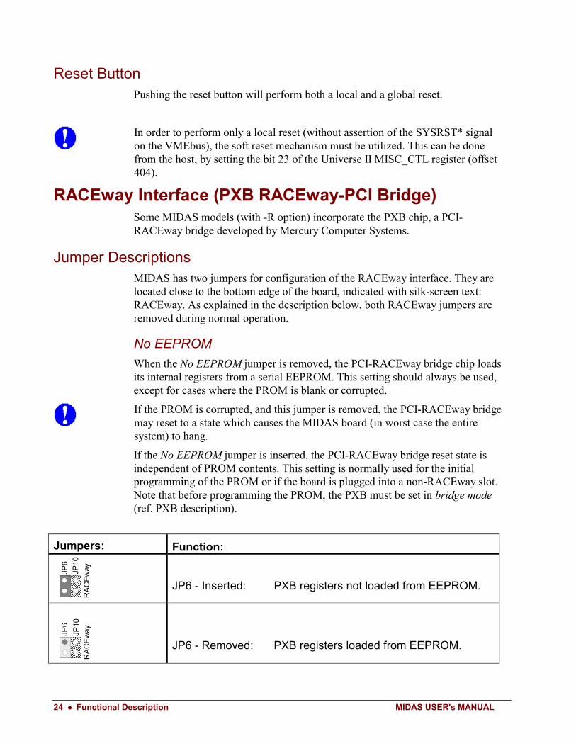
RACEway Interface (PXB RACEway-PCI Bridge)Some MIDAS models (with -R option) incorporate the PXB chip, a PCI-RACEway bridge developed by Mercury Computer Systems.
Jumper DescriptionsMIDAS has two jumpers for configuration of the RACEway interface. They arelocated close to the bottom edge of the board, indicated with silk-screen text:RACEway. As explained in the description below, both RACEway jumpers areremoved during normal operation.
No EEPROM
When the No EEPROM jumper is removed, the PCI-RACEway bridge chip loadsits internal registers from a serial EEPROM. This setting should always be used,except for cases where the PROM is blank or corrupted.
If the PROM is corrupted, and this jumper is removed, the PCI-RACEway bridgemay reset to a state which causes the MIDAS board (in worst case the entiresystem) to hang.
If the No EEPROM jumper is inserted, the PCI-RACEway bridge reset state isindependent of PROM contents. This setting is normally used for the initialprogramming of the PROM or if the board is plugged into a non-RACEway slot.Note that before programming the PROM, the PXB must be set in bridge mode(ref. PXB description).
Jumpers: Function:
���������������������������
JP6
RA
CE
wayJP
10
JP6 - Inserted: PXB registers not loaded from EEPROM.
���������������������������
JP6
RA
CE
wayJP
10
JP6 - Removed: PXB registers loaded from EEPROM.
MIDAS USER's MANUAL Functional Description •••• 25
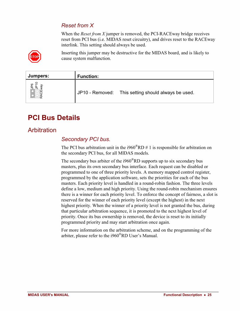
Reset from X
When the Reset from X jumper is removed, the PCI-RACEway bridge receivesreset from PCI bus (i.e. MIDAS reset circuitry), and drives reset to the RACEwayinterlink. This setting should always be used.
Inserting this jumper may be destructive for the MIDAS board, and is likely tocause system malfunction.
Jumpers: Function:
���������������������
JP6
RA
CE
wayJP
10
JP10 - Removed: This setting should always be used.
PCI Bus Details
Arbitration
Secondary PCI bus.
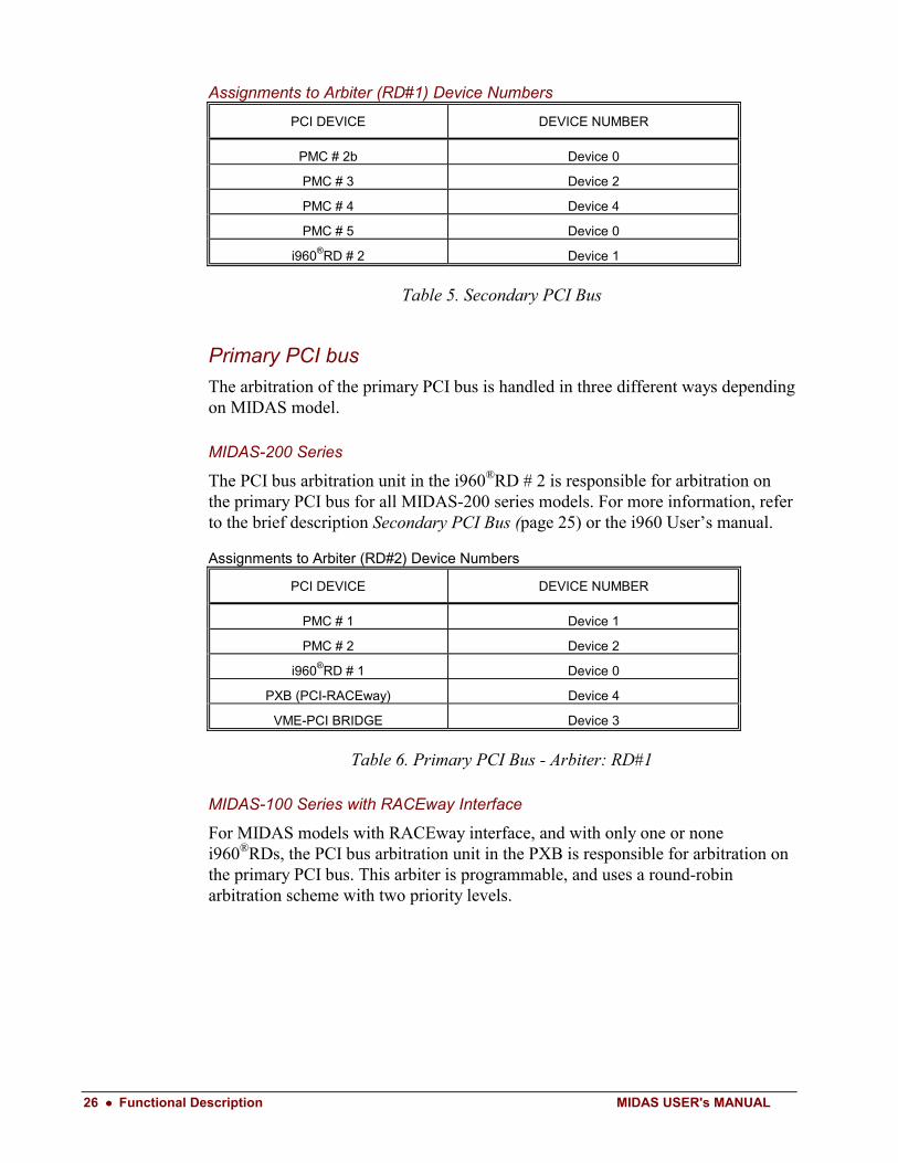
The PCI bus arbitration unit in the i960®RD # 1 is responsible for arbitration onthe secondary PCI bus, for all MIDAS models.
The secondary bus arbiter of the i960®RD supports up to six secondary busmasters, plus its own secondary bus interface. Each request can be disabled orprogrammed to one of three priority levels. A memory mapped control register,programmed by the application software, sets the priorities for each of the busmasters. Each priority level is handled in a round-robin fashion. The three levelsdefine a low, medium and high priority. Using the round-robin mechanism ensuresthere is a winner for each priority level. To enforce the concept of fairness, a slot isreserved for the winner of each priority level (except the highest) in the nexthighest priority. When the winner of a priority level is not granted the bus, duringthat particular arbitration sequence, it is promoted to the next highest level ofpriority. Once its bus ownership is removed, the device is reset to its initiallyprogrammed priority and may start arbitration once again.
For more information on the arbitration scheme, and on the programming of thearbiter, please refer to the i960®RD User’s Manual.
26 •••• Functional Description MIDAS USER's MANUAL
Assignments to Arbiter (RD#1) Device Numbers
PCI DEVICE DEVICE NUMBER
PMC # 2b Device 0
PMC # 3 Device 2
PMC # 4 Device 4
PMC # 5 Device 0
i960®RD # 2 Device 1
Table 5. Secondary PCI Bus
Primary PCI bus
The arbitration of the primary PCI bus is handled in three different ways dependingon MIDAS model.
MIDAS-200 Series
The PCI bus arbitration unit in the i960®RD # 2 is responsible for arbitration onthe primary PCI bus for all MIDAS-200 series models. For more information, referto the brief description Secondary PCI Bus (page 25) or the i960 User’s manual.
Assignments to Arbiter (RD#2) Device Numbers
PCI DEVICE DEVICE NUMBER
PMC # 1 Device 1
PMC # 2 Device 2
i960®RD # 1 Device 0
PXB (PCI-RACEway) Device 4
VME-PCI BRIDGE Device 3
Table 6. Primary PCI Bus - Arbiter: RD#1
MIDAS-100 Series with RACEway Interface
For MIDAS models with RACEway interface, and with only one or nonei960®RDs, the PCI bus arbitration unit in the PXB is responsible for arbitration onthe primary PCI bus. This arbiter is programmable, and uses a round-robinarbitration scheme with two priority levels.
MIDAS USER's MANUAL Functional Description •••• 27
Assignments to Arbiter (PXB) Req/Gnt Pairs
PCI DEVICE Req/Gnt Pairs
PMC # 1 Req1/Gnt1
PMC # 2 Req2/Gnt2
i960®RD # 1 Req4/Gnt4
VME-PCI BRIDGE Req3/Gnt3
Table 7. Primary PCI Bus - Arbiter: PXB
Other MIDAS-1x0 Models
For MIDAS-120 and -150 models without RACEway interface, the arbiter for theprimary PCI bus is implemented in a PLD. This arbiter uses a single level round-robin arbitration scheme.
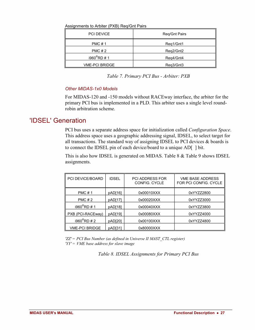
'IDSEL' GenerationPCI bus uses a separate address space for initialization called Configuration Space.This address space uses a geographic addressing signal, IDSEL, to select target forall transactions. The standard way of assigning IDSEL to PCI devices & boards isto connect the IDSEL pin of each device/board to a unique AD[ ] bit.
This is also how IDSEL is generated on MIDAS. Table 8 & Table 9 shows IDSELassignments.
PCI DEVICE/BOARD IDSEL PCI ADDRESS FORCONFIG. CYCLE
VME BASE ADDRESSFOR PCI CONFIG. CYCLE
PMC # 1 pAD[16] 0x00010XXX 0xYYZZ2800
PMC # 2 pAD[17] 0x00020XXX 0xYYZZ3000
i960®RD # 1 pAD[18] 0x00040XXX 0xYYZZ3800
PXB (PCI-RACEway) pAD[19] 0x00080XXX 0xYYZZ4000
i960®RD # 2 pAD[20] 0x00100XXX 0xYYZZ4800
VME-PCI BRIDGE pAD[31] 0x80000XXX
'ZZ' = PCI Bus Number (as defined in Universe II MAST_CTL register)'YY' = VME base address for slave image
Table 8. IDSEL Assignments for Primary PCI Bus
28 •••• Functional Description MIDAS USER's MANUAL
PCI DEVICE/BOARD IDSEL PCI ADDRESS FORCONFIG. CYCLE
VME BASE ADDRESSFOR PCI CONFIG. CYCLE
PMC # 3 sAD[16] 0x00010XXX 0xYYWW0000
PMC # 4 sAD[17] 0x00020XXX 0xYYWW0800
PMC # 5 sAD[18] 0x00040XXX 0xYYWW1000
PMC # 2b sAD[19] 0x00080XXX 0xYYWW1800
i960®RD # 1 sAD[21] 0x00200XXX 0xYYWW2800
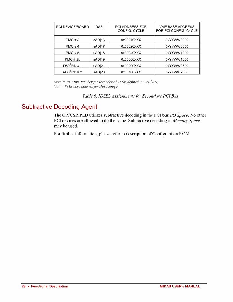
i960®RD # 2 sAD[20] 0x00100XXX 0xYYWW2000
'WW' = PCI Bus Number for secondary bus (as defined in i960®RD)'YY' = VME base address for slave image
Table 9. IDSEL Assignments for Secondary PCI Bus
Subtractive Decoding AgentThe CR/CSR PLD utilizes subtractive decoding in the PCI bus I/O Space. No otherPCI devices are allowed to do the same. Subtractive decoding in Memory Spacemay be used.
For further information, please refer to description of Configuration ROM.
MIDAS USER's MANUAL Functional Description •••• 29
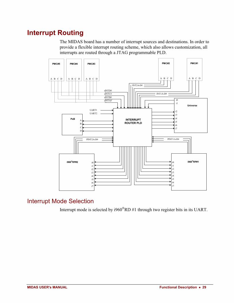
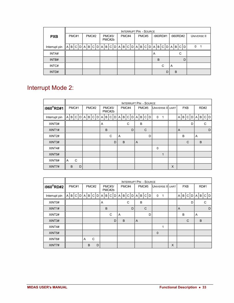
Interrupt RoutingThe MIDAS board has a number of interrupt sources and destinations. In order toprovide a flexible interrupt routing scheme, which also allows customization, allinterrupts are routed through a JTAG programmable PLD.
PINT2A-D#
i4
i6
i7
i2
i3
i0
i1
i960®RP#2
i5
PINT1A-D#
i4
i6
i7
i2
i3
i0
i1
i960®RP#1
i5
sINTD#
sINTC#
sINTB#
sINTA#
UART1
UART2
INTERRUPTROUTER PLD
PMC#2
DCBA
PMC#1
DCBA
PMC#4
DCBA
PMC#3
DCBA
PMC#5
DCBA
i6
i4
i5
i2
i3
i0
i1Universe
i7
INT1A-D#
INT2A-D#
C
D
A
B
PxB
Interrupt Mode SelectionInterrupt mode is selected by i960®RD #1 through two register bits in its UART.
30 •••• Functional Description MIDAS USER's MANUAL
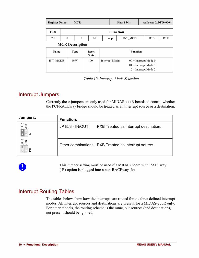
Register Name: MCR Size: 8 bits Address: 0xDF00.0004
Bits Function
7:0 0 0 AFE Loop INT_MODE RTS DTR
MCR Description
Name Type ResetState
Function
INT_MODE R/W 00 Interrupt Mode: 00 = Interrupt Mode 0
01 = Interrupt Mode 1
10 = Interrupt Mode 2
Table 10. Interrupt Mode Selection
Interrupt JumpersCurrently these jumpers are only used for MIDAS-xxxR boards to control whetherthe PCI-RACEway bridge should be treated as an interrupt source or a destination.
Jumpers: Function:
JP15
INT
JP3
JP15/3 - IN/OUT: PXB Treated as interrupt destination.
JP15
INT
JP3
Other combinations: PXB Treated as interrupt source.
This jumper setting must be used if a MIDAS board with RACEway(-R) option is plugged into a non-RACEway slot.
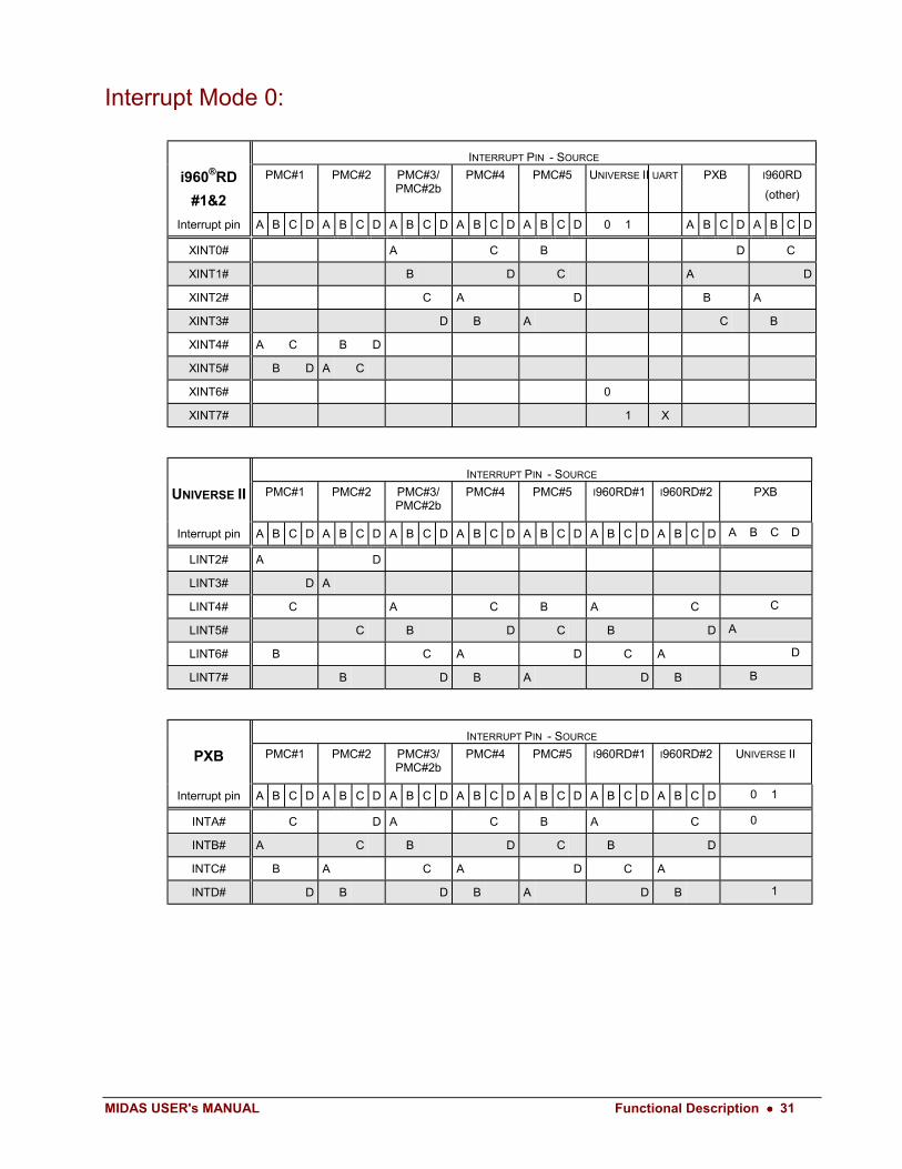
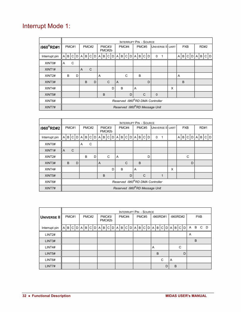
Interrupt Routing TablesThe tables below show how the interrupts are routed for the three defined interruptmodes. All interrupt sources and destinations are present for a MIDAS-250R only.For other models, the routing scheme is the same, but sources (and destinations)not present should be ignored.
MIDAS USER's MANUAL Functional Description •••• 31
Interrupt Mode 0:
INTERRUPT PIN - SOURCE
i960®RD
#1&2
PMC#1 PMC#2 PMC#3/PMC#2b
PMC#4 PMC#5 UNIVERSE II UART PXB I960RD
(other)
Interrupt pin A B C D A B C D A B C D A B C D A B C D 0 1 A B C D A B C D
XINT0# A C B D C
XINT1# B D C A D
XINT2# C A D B A
XINT3# D B A C B
XINT4# A C B D
XINT5# B D A C
XINT6# 0
XINT7# 1 X
INTERRUPT PIN - SOURCE
UNIVERSE II PMC#1 PMC#2 PMC#3/PMC#2b
PMC#4 PMC#5 I960RD#1 I960RD#2 PXB
Interrupt pin A B C D A B C D A B C D A B C D A B C D A B C D A B C D A B C D
LINT2# A D
LINT3# D A
LINT4# C A C B A C C
LINT5# C B D C B D A
LINT6# B C A D C A D
LINT7# B D B A D B B
INTERRUPT PIN - SOURCE
PXB PMC#1 PMC#2 PMC#3/PMC#2b
PMC#4 PMC#5 I960RD#1 I960RD#2 UNIVERSE II
Interrupt pin A B C D A B C D A B C D A B C D A B C D A B C D A B C D 0 1
INTA# C D A C B A C 0
INTB# A C B D C B D
INTC# B A C A D C A
INTD# D B D B A D B 1
32 •••• Functional Description MIDAS USER's MANUAL
Interrupt Mode 1:
INTERRUPT PIN - SOURCE
i960®RD#1 PMC#1 PMC#2 PMC#3/PMC#2b
PMC#4 PMC#5 UNIVERSE II UART PXB RD#2
Interrupt pin A B C D A B C D A B C D A B C D A B C D 0 1 A B C D A B C D
XINT0# A C
XINT1# A C
XINT2# B D A C B A
XINT3# B D C A D B
XINT4# D B A X
XINT5# B D C 0
XINT6# Reserved i960®RD DMA Controller
XINT7# Reserved i960®RD Message Unit
INTERRUPT PIN - SOURCE
i960®RD#2 PMC#1 PMC#2 PMC#3/PMC#2b
PMC#4 PMC#5 UNIVERSE II UART PXB RD#1
Interrupt pin A B C D A B C D A B C D A B C D A B C D 0 1 A B C D A B C D
XINT0# A C
XINT1# A C
XINT2# B D C A D C
XINT3# B D A C B D
XINT4# D B A X
XINT5# B D C 1
XINT6# Reserved i960®RD DMA Controller
XINT7# Reserved i960®RD Message Unit
INTERRUPT PIN - SOURCE
UNIVERSE II PMC#1 PMC#2 PMC#3/PMC#2b
PMC#4 PMC#5 I960RD#1 I960RD#2 PXB
Interrupt pin A B C D A B C D A B C D A B C D A B C D A B C D A B C D A B C D
LINT2# A
LINT3# B
LINT4# A C
LINT5# B D
LINT6# C A
LINT7# D B
MIDAS USER's MANUAL Functional Description •••• 33
INTERRUPT PIN - SOURCE
PXB PMC#1 PMC#2 PMC#3/PMC#2b
PMC#4 PMC#5 I960RD#1 I960RD#2 UNIVERSE II
Interrupt pin A B C D A B C D A B C D A B C D A B C D A B C D A B C D 0 1
INTA# A C
INTB# B D
INTC# C A
INTD# D B
Interrupt Mode 2:
INTERRUPT PIN - SOURCE
i960®RD#1 PMC#1 PMC#2 PMC#3/PMC#2b
PMC#4 PMC#5 UNIVERSE II UART PXB RD#2
Interrupt pin A B C D A B C D A B C D A B C D A B C D 0 1 A B C D A B C D
XINT0# A C B D C
XINT1# B D C A D
XINT2# C A D B A
XINT3# D B A C B
XINT4# 0
XINT5# 1
XINT6# A C
XINT7# B D X
INTERRUPT PIN - SOURCE
i960®RD#2 PMC#1 PMC#2 PMC#3/PMC#2b
PMC#4 PMC#5 UNIVERSE II UART PXB RD#1
Interrupt pin A B C D A B C D A B C D A B C D A B C D 0 1 A B C D A B C D
XINT0# A C B D C
XINT1# B D C A D
XINT2# C A D B A
XINT3# D B A C B
XINT4# 1
XINT5# 0
XINT6# A C
XINT7# B D X
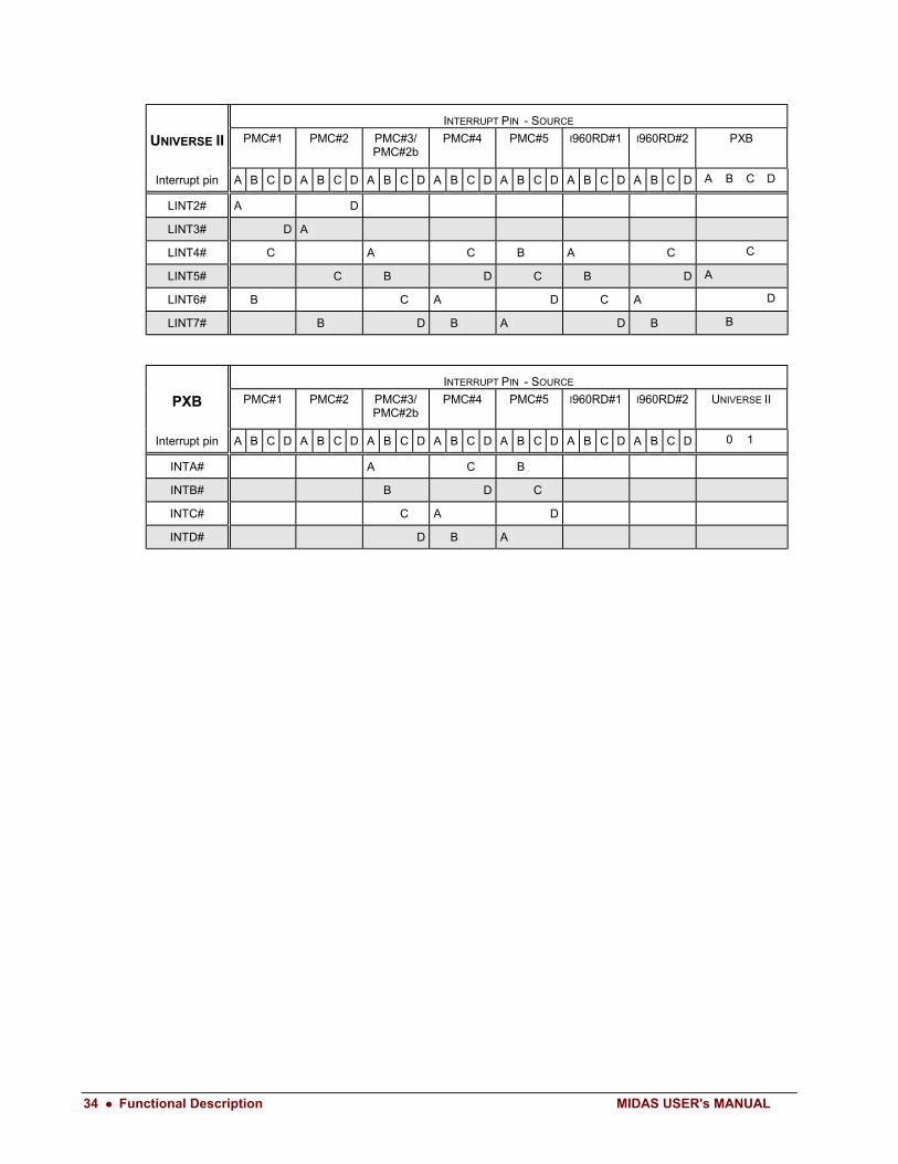
34 •••• Functional Description MIDAS USER's MANUAL
INTERRUPT PIN - SOURCE
UNIVERSE II PMC#1 PMC#2 PMC#3/PMC#2b
PMC#4 PMC#5 I960RD#1 I960RD#2 PXB
Interrupt pin A B C D A B C D A B C D A B C D A B C D A B C D A B C D A B C D
LINT2# A D
LINT3# D A
LINT4# C A C B A C C
LINT5# C B D C B D A
LINT6# B C A D C A D
LINT7# B D B A D B B
INTERRUPT PIN - SOURCE
PXB PMC#1 PMC#2 PMC#3/PMC#2b
PMC#4 PMC#5 I960RD#1 I960RD#2 UNIVERSE II
Interrupt pin A B C D A B C D A B C D A B C D A B C D A B C D A B C D 0 1
INTA# A C B
INTB# B D C
INTC# C A D
INTD# D B A
MIDAS USER's MANUAL Appendix I: PMC I/O Routing •••• 35
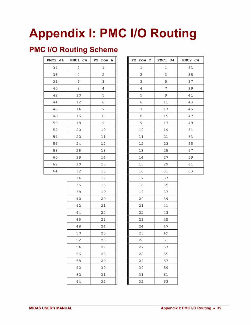
Appendix I: PMC I/O RoutingPMC I/O Routing Scheme
PMC2 J4 PMC1 J4 P2 row A P2 row C PMC1 J4 PMC2 J4
34 2 1 1 1 33
36 4 2 2 3 35
38 6 3 3 5 37
40 8 4 4 7 39
42 10 5 5 9 41
44 12 6 6 11 43
46 14 7 7 13 45
48 16 8 8 15 47
50 18 9 9 17 49
52 20 10 10 19 51
54 22 11 11 21 53
56 24 12 12 23 55
58 26 13 13 25 57
60 28 14 14 27 59
62 30 15 15 29 61
64 32 16 16 31 63
34 17 17 33
36 18 18 35
38 19 19 37
40 20 20 39
42 21 21 41
44 22 22 43
46 23 23 45
48 24 24 47
50 25 25 49
52 26 26 51
54 27 27 53
56 28 28 55
58 29 29 57
60 30 30 59
62 31 31 61
64 32 32 63
36 •••• Appendix II: Universe II Configuration Examples MIDAS USER's MANUAL
Appendix II: Universe IIConfiguration Examples
General InformationNote that the 'Universe II' PCI-VME Bridge, performs byte swapping of the datalanes on all transactions between VMEbus and PCI bus. This is also the case foraccesses to the internal registers. The internal register bank is located on the 'PCIside' of the byte swapping. This means that when registers are read or writtenfrom the VMEbus, all bytes are shuffled (compared to the bit numbering used inthe Universe II User Manual).
VMEbus Slave Images
PCI Master EnableIn addition to the configuration registers for the VMEbus slave images, one controlregister bit is essential for mapping VMEbus cycles to PCI bus cycles through theUniverse II. The PCI master enable ('BM') bit located in the PCI_CSR registerspace (offset: 0x004). This bit is set as default after power up.
Some VMEbus Slave Image examples are shown in Figure 14.
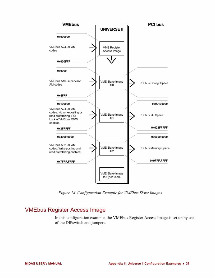
MIDAS USER's MANUAL Appendix II: Universe II Configuration Examples •••• 37
PCI busVMEbus
VME Slave Image# 0
VMEbus A16, supervisorAM codes
0x4FFF
0x0000
UNIVERSE II
PCI bus Config. Space
VME Slave Image# 1
VMEbus A24, all AMcodes, No write-posting orread prefetching. PCILock of VMEbus RMWenabled.
0x3FFFFF
0x100000
0x023FFFFF
0x02100000
PCI bus I/O Space.
VME Slave Image# 3 (not used)
VME Slave Image# 2
VMEbus A32, all AMcodes, Write-posting andread prefetching enabled.
0x7FFF.FFFF
0x4000.0000
0x9FFF.FFFF
0x6000.0000
PCI bus Memory Space.
VME RegisterAccess Image
VMEbus A24, all AMcodes
0x000FFF
0x000000
Figure 14. Configuration Example for VMEbus Slave Images
VMEbus Register Access ImageIn this configuration example, the VMEbus Register Access Image is set up by useof the DIPswitch and jumpers.
38 •••• Appendix II: Universe II Configuration Examples MIDAS USER's MANUAL
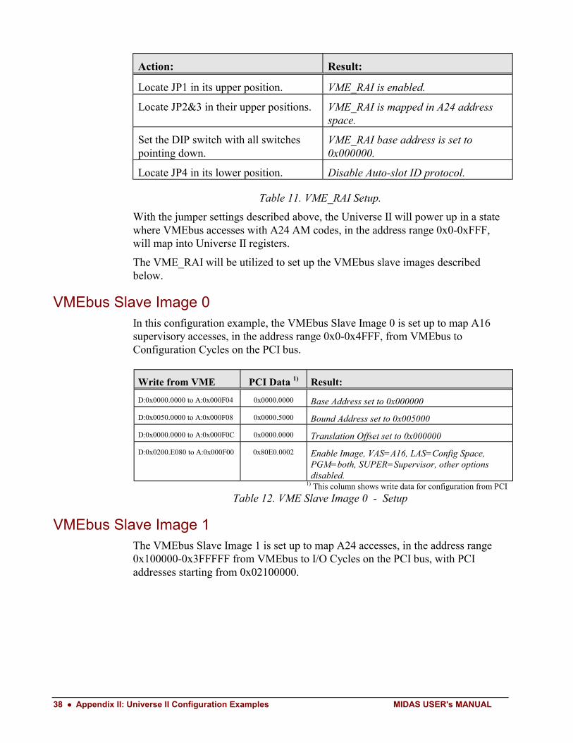
Action: Result:
Locate JP1 in its upper position. VME_RAI is enabled.
Locate JP2&3 in their upper positions. VME_RAI is mapped in A24 addressspace.
Set the DIP switch with all switchespointing down.
VME_RAI base address is set to0x000000.
Locate JP4 in its lower position. Disable Auto-slot ID protocol.
Table 11. VME_RAI Setup.
With the jumper settings described above, the Universe II will power up in a statewhere VMEbus accesses with A24 AM codes, in the address range 0x0-0xFFF,will map into Universe II registers.
The VME_RAI will be utilized to set up the VMEbus slave images describedbelow.
VMEbus Slave Image 0In this configuration example, the VMEbus Slave Image 0 is set up to map A16supervisory accesses, in the address range 0x0-0x4FFF, from VMEbus toConfiguration Cycles on the PCI bus.
Write from VME PCI Data 1) Result:
D:0x0000.0000 to A:0x000F04 0x0000.0000 Base Address set to 0x000000
D:0x0050.0000 to A:0x000F08 0x0000.5000 Bound Address set to 0x005000
D:0x0000.0000 to A:0x000F0C 0x0000.0000 Translation Offset set to 0x000000
D:0x0200.E080 to A:0x000F00 0x80E0.0002 Enable Image, VAS=A16, LAS=Config Space,PGM=both, SUPER=Supervisor, other optionsdisabled.
1) This column shows write data for configuration from PCI
Table 12. VME Slave Image 0 - Setup
VMEbus Slave Image 1The VMEbus Slave Image 1 is set up to map A24 accesses, in the address range0x100000-0x3FFFFF from VMEbus to I/O Cycles on the PCI bus, with PCIaddresses starting from 0x02100000.
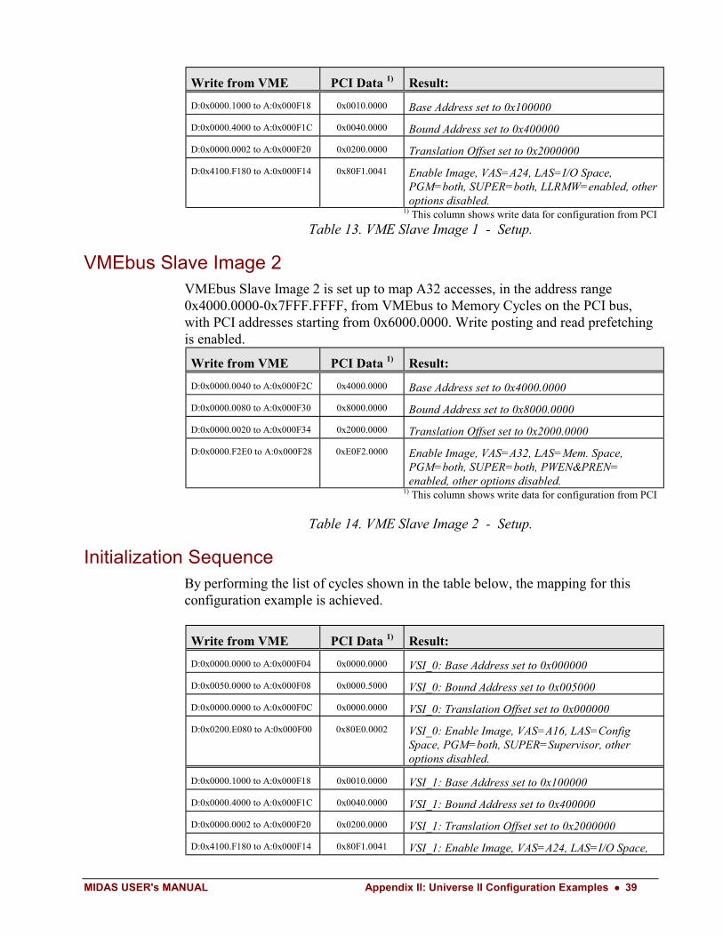
MIDAS USER's MANUAL Appendix II: Universe II Configuration Examples •••• 39
Write from VME PCI Data 1) Result:
D:0x0000.1000 to A:0x000F18 0x0010.0000 Base Address set to 0x100000
D:0x0000.4000 to A:0x000F1C 0x0040.0000 Bound Address set to 0x400000
D:0x0000.0002 to A:0x000F20 0x0200.0000 Translation Offset set to 0x2000000
D:0x4100.F180 to A:0x000F14 0x80F1.0041 Enable Image, VAS=A24, LAS=I/O Space,PGM=both, SUPER=both, LLRMW=enabled, otheroptions disabled.
1) This column shows write data for configuration from PCI
Table 13. VME Slave Image 1 - Setup.
VMEbus Slave Image 2VMEbus Slave Image 2 is set up to map A32 accesses, in the address range0x4000.0000-0x7FFF.FFFF, from VMEbus to Memory Cycles on the PCI bus,with PCI addresses starting from 0x6000.0000. Write posting and read prefetchingis enabled.
Write from VME PCI Data 1) Result:
D:0x0000.0040 to A:0x000F2C 0x4000.0000 Base Address set to 0x4000.0000
D:0x0000.0080 to A:0x000F30 0x8000.0000 Bound Address set to 0x8000.0000
D:0x0000.0020 to A:0x000F34 0x2000.0000 Translation Offset set to 0x2000.0000
D:0x0000.F2E0 to A:0x000F28 0xE0F2.0000 Enable Image, VAS=A32, LAS=Mem. Space,PGM=both, SUPER=both, PWEN&PREN=enabled, other options disabled.
1) This column shows write data for configuration from PCI
Table 14. VME Slave Image 2 - Setup.
Initialization SequenceBy performing the list of cycles shown in the table below, the mapping for thisconfiguration example is achieved.
Write from VME PCI Data 1) Result:
D:0x0000.0000 to A:0x000F04 0x0000.0000 VSI_0: Base Address set to 0x000000
D:0x0050.0000 to A:0x000F08 0x0000.5000 VSI_0: Bound Address set to 0x005000
D:0x0000.0000 to A:0x000F0C 0x0000.0000 VSI_0: Translation Offset set to 0x000000
D:0x0200.E080 to A:0x000F00 0x80E0.0002 VSI_0: Enable Image, VAS=A16, LAS=ConfigSpace, PGM=both, SUPER=Supervisor, otheroptions disabled.
D:0x0000.1000 to A:0x000F18 0x0010.0000 VSI_1: Base Address set to 0x100000
D:0x0000.4000 to A:0x000F1C 0x0040.0000 VSI_1: Bound Address set to 0x400000
D:0x0000.0002 to A:0x000F20 0x0200.0000 VSI_1: Translation Offset set to 0x2000000
D:0x4100.F180 to A:0x000F14 0x80F1.0041 VSI_1: Enable Image, VAS=A24, LAS=I/O Space,
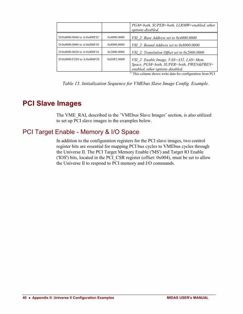
40 •••• Appendix II: Universe II Configuration Examples MIDAS USER's MANUAL
PGM=both, SUPER=both, LLRMW=enabled, otheroptions disabled.
D:0x0000.0040 to A:0x000F2C 0x4000.0000 VSI_2: Base Address set to 0x4000.0000
D:0x0000.0080 to A:0x000F30 0x8000.0000 VSI_2: Bound Address set to 0x8000.0000
D:0x0000.0020 to A:0x000F34 0x2000.0000 VSI_2: Translation Offset set to 0x2000.0000
D:0x0000.F2E0 to A:0x000F28 0xE0F2.0000 VSI_2: Enable Image, VAS=A32, LAS=Mem.Space, PGM=both, SUPER=both, PWEN&PREN=enabled, other options disabled.
1) This column shows write data for configuration from PCI
Table 15. Initialization Sequence for VMEbus Slave Image Config. Example.
PCI Slave Images
The VME_RAI, described in the ’VMEbus Slave Images’ section, is also utilizedto set up PCI slave images in the examples below.
PCI Target Enable - Memory & I/O SpaceIn addition to the configuration registers for the PCI slave images, two controlregister bits are essential for mapping PCI bus cycles to VMEbus cycles throughthe Universe II. The PCI Target Memory Enable ('MS') and Target IO Enable('IOS') bits, located in the PCI_CSR register (offset: 0x004), must be set to allowthe Universe II to respond to PCI memory and I/O commands.
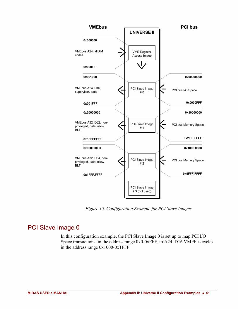
MIDAS USER's MANUAL Appendix II: Universe II Configuration Examples •••• 41
PCI busVMEbus
PCI Slave Image# 0
VMEbus A24, D16,supervisor, data
0x001FFF
0x001000
UNIVERSE II
0x0000FFF
0x00000000
PCI bus I/O Space
PCI Slave Image# 1
VMEbus A32, D64, non-privileged, data, allowBLT.
VMEbus A32, D32, non-privileged, data, allowBLT.
0x3FFFFFFF
0x20000000
0x2FFFFFFF
0x10000000
PCI bus Memory Space.
PCI Slave Image# 3 (not used)
PCI Slave Image# 2
0x1FFF.FFFF
0x0000.0000
0x5FFF.FFFF
0x4000.0000
PCI bus Memory Space.
VME RegisterAccess Image
VMEbus A24, all AMcodes
0x000FFF
0x000000
Figure 15. Configuration Example for PCI Slave Images
PCI Slave Image 0In this configuration example, the PCI Slave Image 0 is set up to map PCI I/OSpace transactions, in the address range 0x0-0xFFF, to A24, D16 VMEbus cycles,in the address range 0x1000-0x1FFF.
42 •••• Appendix II: Universe II Configuration Examples MIDAS USER's MANUAL
Write from VME PCI Data 1) Result:
D:0x0000.0000 to A:0x000104 0x0000.0000 Base Address set to 0x0000.0000
D:0x0010.0000 to A:0x000108 0x0000.1000 Bound Address set to 0x0000.1000
D:0x0010.0000 to A:0x00010C 0x0000.1000 Translation Offset set to 0x0000.1000
D:0x0110.4180 to A:0x000100 0x8041.1001 Enable Image, VAS=A24, VDW=D16, LAS=I/OSpace, PGM=data, SUPER=supervisor, otheroptions disabled.
1) This column shows write data for configuration from PCI
Table 16. PCI Slave Image 0 Setup.
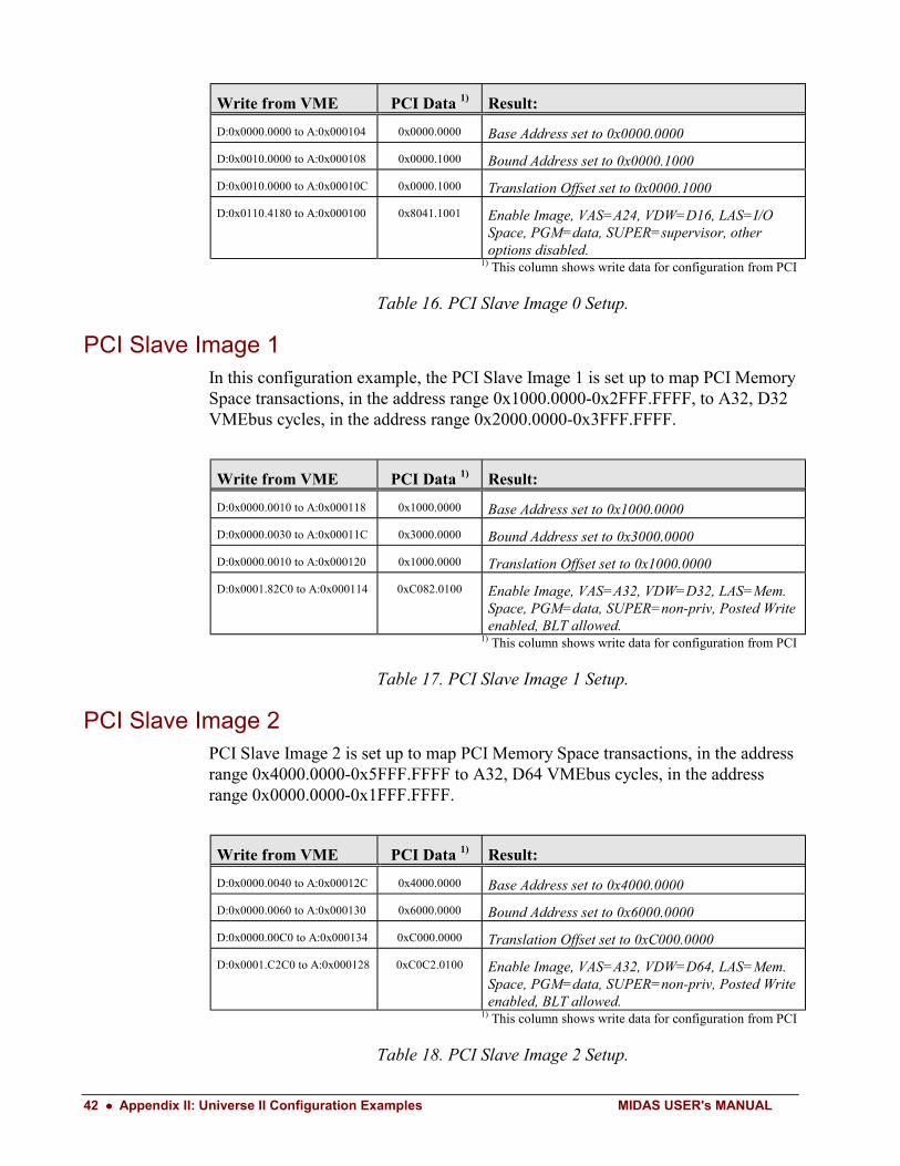
PCI Slave Image 1In this configuration example, the PCI Slave Image 1 is set up to map PCI MemorySpace transactions, in the address range 0x1000.0000-0x2FFF.FFFF, to A32, D32VMEbus cycles, in the address range 0x2000.0000-0x3FFF.FFFF.
Write from VME PCI Data 1) Result:
D:0x0000.0010 to A:0x000118 0x1000.0000 Base Address set to 0x1000.0000
D:0x0000.0030 to A:0x00011C 0x3000.0000 Bound Address set to 0x3000.0000
D:0x0000.0010 to A:0x000120 0x1000.0000 Translation Offset set to 0x1000.0000
D:0x0001.82C0 to A:0x000114 0xC082.0100 Enable Image, VAS=A32, VDW=D32, LAS=Mem.Space, PGM=data, SUPER=non-priv, Posted Writeenabled, BLT allowed.
1) This column shows write data for configuration from PCI
Table 17. PCI Slave Image 1 Setup.
PCI Slave Image 2PCI Slave Image 2 is set up to map PCI Memory Space transactions, in the addressrange 0x4000.0000-0x5FFF.FFFF to A32, D64 VMEbus cycles, in the addressrange 0x0000.0000-0x1FFF.FFFF.
Write from VME PCI Data 1) Result:
D:0x0000.0040 to A:0x00012C 0x4000.0000 Base Address set to 0x4000.0000
D:0x0000.0060 to A:0x000130 0x6000.0000 Bound Address set to 0x6000.0000
D:0x0000.00C0 to A:0x000134 0xC000.0000 Translation Offset set to 0xC000.0000
D:0x0001.C2C0 to A:0x000128 0xC0C2.0100 Enable Image, VAS=A32, VDW=D64, LAS=Mem.Space, PGM=data, SUPER=non-priv, Posted Writeenabled, BLT allowed.
1) This column shows write data for configuration from PCI
Table 18. PCI Slave Image 2 Setup.
MIDAS USER's MANUAL Appendix II: Universe II Configuration Examples •••• 43
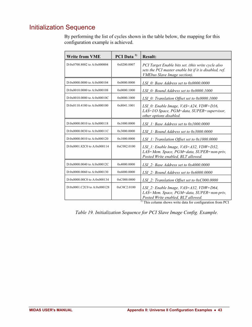
Initialization SequenceBy performing the list of cycles shown in the table below, the mapping for thisconfiguration example is achieved.
Write from VME PCI Data 1) Result:
D:0x0700.8002 to A:0x000004 0x0200.0007 PCI Target Enable bits set. (this write cycle alsosets the PCI master enable bit if it is disabled, ref.VMEbus Slave Image section).
D:0x0000.0000 to A:0x000104 0x0000.0000 LSI_0: Base Address set to 0x0000.0000
D:0x0010.0000 to A:0x000108 0x0000.1000 LSI_0: Bound Address set to 0x0000.1000
D:0x0010.0000 to A:0x00010C 0x0000.1000 LSI_0: Translation Offset set to 0x0000.1000
D:0x0110.4180 to A:0x000100 0x8041.1001 LSI_0: Enable Image, VAS=A24, VDW=D16,LAS=I/O Space, PGM=data, SUPER=supervisor,other options disabled.
D:0x0000.0010 to A:0x000118 0x1000.0000 LSI_1: Base Address set to 0x1000.0000
D:0x0000.0030 to A:0x00011C 0x3000.0000 LSI_1: Bound Address set to 0x3000.0000
D:0x0000.0010 to A:0x000120 0x1000.0000 LSI_1: Translation Offset set to 0x1000.0000
D:0x0001.82C0 to A:0x000114 0xC082.0100 LSI_1: Enable Image, VAS=A32, VDW=D32,LAS=Mem. Space, PGM=data, SUPER=non-priv,Posted Write enabled, BLT allowed.
D:0x0000.0040 to A:0x00012C 0x4000.0000 LSI_2: Base Address set to 0x4000.0000
D:0x0000.0060 to A:0x000130 0x6000.0000 LSI_2: Bound Address set to 0x6000.0000
D:0x0000.00C0 to A:0x000134 0xC000.0000 LSI_2: Translation Offset set to 0xC000.0000
D:0x0001.C2C0 to A:0x000128 0xC0C2.0100 LSI_2: Enable Image, VAS=A32, VDW=D64,LAS=Mem. Space, PGM=data, SUPER=non-priv,Posted Write enabled, BLT allowed.
1) This column shows write data for configuration from PCI
Table 19. Initialization Sequence for PCI Slave Image Config. Example.
44 •••• Appendix III: PXB Information MIDAS USER's MANUAL
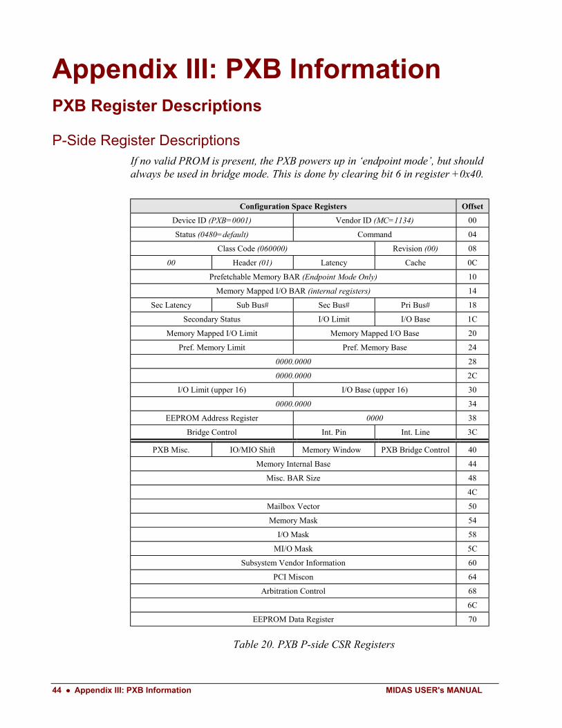
Appendix III: PXB InformationPXB Register Descriptions
P-Side Register DescriptionsIf no valid PROM is present, the PXB powers up in ‘endpoint mode’, but shouldalways be used in bridge mode. This is done by clearing bit 6 in register +0x40.
Configuration Space Registers Offset
Device ID (PXB=0001) Vendor ID (MC=1134) 00
Status (0480=default) Command 04
Class Code (060000) Revision (00) 08
00 Header (01) Latency Cache 0C
Prefetchable Memory BAR (Endpoint Mode Only) 10
Memory Mapped I/O BAR (internal registers) 14
Sec Latency Sub Bus# Sec Bus# Pri Bus# 18
Secondary Status I/O Limit I/O Base 1C
Memory Mapped I/O Limit Memory Mapped I/O Base 20
Pref. Memory Limit Pref. Memory Base 24
0000.0000 28
0000.0000 2C
I/O Limit (upper 16) I/O Base (upper 16) 30
0000.0000 34
EEPROM Address Register 0000 38
Bridge Control Int. Pin Int. Line 3C
PXB Misc. IO/MIO Shift Memory Window PXB Bridge Control 40
Memory Internal Base 44
Misc. BAR Size 48
4C
Mailbox Vector 50
Memory Mask 54
I/O Mask 58
MI/O Mask 5C
Subsystem Vendor Information 60
PCI Miscon 64
Arbitration Control 68
6C
EEPROM Data Register 70
Table 20. PXB P-side CSR Registers
MIDAS USER's MANUAL Appendix III: PXB Information •••• 45
'PCI Command Register'
Register Name: PCMDR Size: 16 bits Offset: 0x04
Bits Function
15:8 RESERVED (000000). 0 SERR_EN
7:0 0 PERR_EN 0 0 0 BM MS IOS
PCMDR Description
Name Type ResetState
Function
SERR_EN R/W 0 SERR Enable
PERR_EN R/W 0 PERR Generation enable
BM R/W 1 PCI Master Enable
MS R/W 1 Memory Space Target Enable
IOS R/W 1 I/O Space Target Enable
Table 21. PCI Command Register
'PCI Status Register'
Register Name: PSR Size: 16 bits Offset: 0x06
Bits Function
15:8 DPE SSE RMAB RTAB STAB DEVSEL DPD
7:0 RESERVED (000000).
PSR Description
Name Type ResetState
Function
DPE R/W Detected parity error
SSE R/W Signaled SERR
RMAB R/W Received Master Abort
RTAB R/W Received Target Abort
STAB R 0 Signaled Target Abort. Always 0.
DEVSEL R 10 DEVSEL Timing. 10=slow.
DPD R/W 0 Data Parity Detected.
Table 22. PCI Status Register
46 •••• Appendix III: PXB Information MIDAS USER's MANUAL
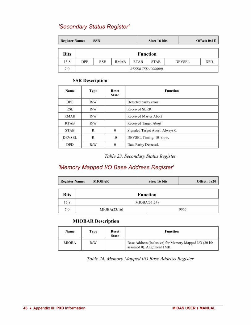
'Secondary Status Register'
Register Name: SSR Size: 16 bits Offset: 0x1E
Bits Function
15:8 DPE RSE RMAB RTAB STAB DEVSEL DPD
7:0 RESERVED (000000).
SSR Description
Name Type ResetState
Function
DPE R/W Detected parity error
RSE R/W Received SERR
RMAB R/W Received Master Abort
RTAB R/W Received Target Abort
STAB R 0 Signaled Target Abort. Always 0.
DEVSEL R 10 DEVSEL Timing. 10=slow.
DPD R/W 0 Data Parity Detected.
Table 23. Secondary Status Register
'Memory Mapped I/O Base Address Register'
Register Name: MIOBAR Size: 16 bits Offset: 0x20
Bits Function
15:8 MIOBA(31:24)
7:0 MIOBA(23:16) 0000
MIOBAR Description
Name Type ResetState
Function
MIOBA R/W Base Address (inclusive) for Memory Mapped I/O (20 lsbassumed 0). Alignment 1MB.
Table 24. Memory Mapped I/O Base Address Register
MIDAS USER's MANUAL Appendix III: PXB Information •••• 47
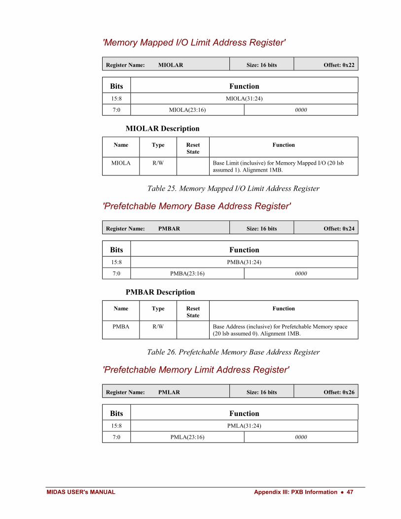
'Memory Mapped I/O Limit Address Register'
Register Name: MIOLAR Size: 16 bits Offset: 0x22
Bits Function
15:8 MIOLA(31:24)
7:0 MIOLA(23:16) 0000
MIOLAR Description
Name Type ResetState
Function
MIOLA R/W Base Limit (inclusive) for Memory Mapped I/O (20 lsbassumed 1). Alignment 1MB.
Table 25. Memory Mapped I/O Limit Address Register
'Prefetchable Memory Base Address Register'
Register Name: PMBAR Size: 16 bits Offset: 0x24
Bits Function
15:8 PMBA(31:24)
7:0 PMBA(23:16) 0000
PMBAR Description
Name Type ResetState
Function
PMBA R/W Base Address (inclusive) for Prefetchable Memory space(20 lsb assumed 0). Alignment 1MB.
Table 26. Prefetchable Memory Base Address Register
'Prefetchable Memory Limit Address Register'
Register Name: PMLAR Size: 16 bits Offset: 0x26
Bits Function
15:8 PMLA(31:24)
7:0 PMLA(23:16) 0000
48 •••• Appendix III: PXB Information MIDAS USER's MANUAL
PMLAR Description
Name Type ResetState
Function
PMLA R/W Base Limit (inclusive) for PrefetchableMemory space (20lsb assumed 1). Alignment 1MB.
Table 27. Prefetchable Memory Limit Address Register
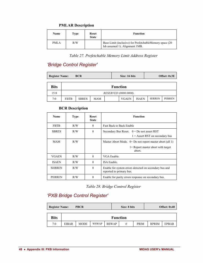
'Bridge Control Register'
Register Name: BCR Size: 16 bits Offset: 0x3E
Bits Function
15:8 RESERVED (0000.0000).
7:0 FBTB SBRES MAM VGAEN ISAEN SERREN PERREN
BCR Description
Name Type ResetState
Function
FBTB R/W 0 Fast Back to Back Enable
SBRES R/W 0 Secondary Bus Reset. 0 = Do not assert RST
1 = Assert RST on secondary bus
MAM R/W Master Abort Mode. 0= Do not report master abort (all 1)
1= Report master abort with targetabort.
VGAEN R/W 0 VGA Enable
ISAEN R/W 0 ISA Enable.
SERREN R/W 0 Enable for system errors detected on secondary bus andreported to primary bus.
PERREN R/W 0 Enable for parity errors response on secondary bus.
Table 28. Bridge Control Register
'PXB Bridge Control Register'
Register Name: PBCR Size: 8 bits Offset: 0x40
Bits Function
7:0 EIBAR MODE WSWAP BSWAP 0 PRIM RPRIM EPBAR
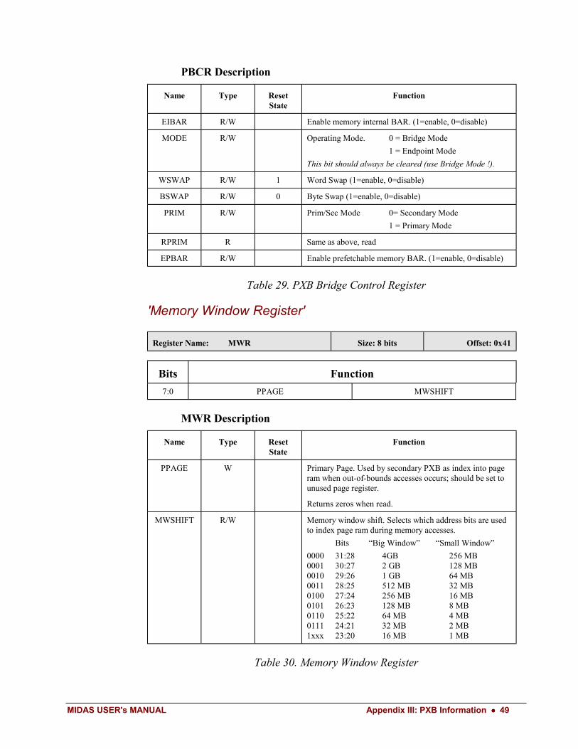
MIDAS USER's MANUAL Appendix III: PXB Information •••• 49
PBCR Description
Name Type ResetState
Function
EIBAR R/W Enable memory internal BAR. (1=enable, 0=disable)
MODE R/W Operating Mode. 0 = Bridge Mode
1 = Endpoint Mode
This bit should always be cleared (use Bridge Mode !).
WSWAP R/W 1 Word Swap (1=enable, 0=disable)
BSWAP R/W 0 Byte Swap (1=enable, 0=disable)
PRIM R/W Prim/Sec Mode 0= Secondary Mode
1 = Primary Mode
RPRIM R Same as above, read
EPBAR R/W Enable prefetchable memory BAR. (1=enable, 0=disable)
Table 29. PXB Bridge Control Register
'Memory Window Register'
Register Name: MWR Size: 8 bits Offset: 0x41
Bits Function
7:0 PPAGE MWSHIFT
MWR Description
Name Type ResetState
Function
PPAGE W Primary Page. Used by secondary PXB as index into pageram when out-of-bounds accesses occurs; should be set tounused page register.
Returns zeros when read.
MWSHIFT R/W Memory window shift. Selects which address bits are usedto index page ram during memory accesses.
Bits “Big Window” “Small Window”
0000 31:28 4GB 256 MB0001 30:27 2 GB 128 MB0010 29:26 1 GB 64 MB0011 28:25 512 MB 32 MB0100 27:24 256 MB 16 MB0101 26:23 128 MB 8 MB0110 25:22 64 MB 4 MB0111 24:21 32 MB 2 MB1xxx 23:20 16 MB 1 MB
Table 30. Memory Window Register
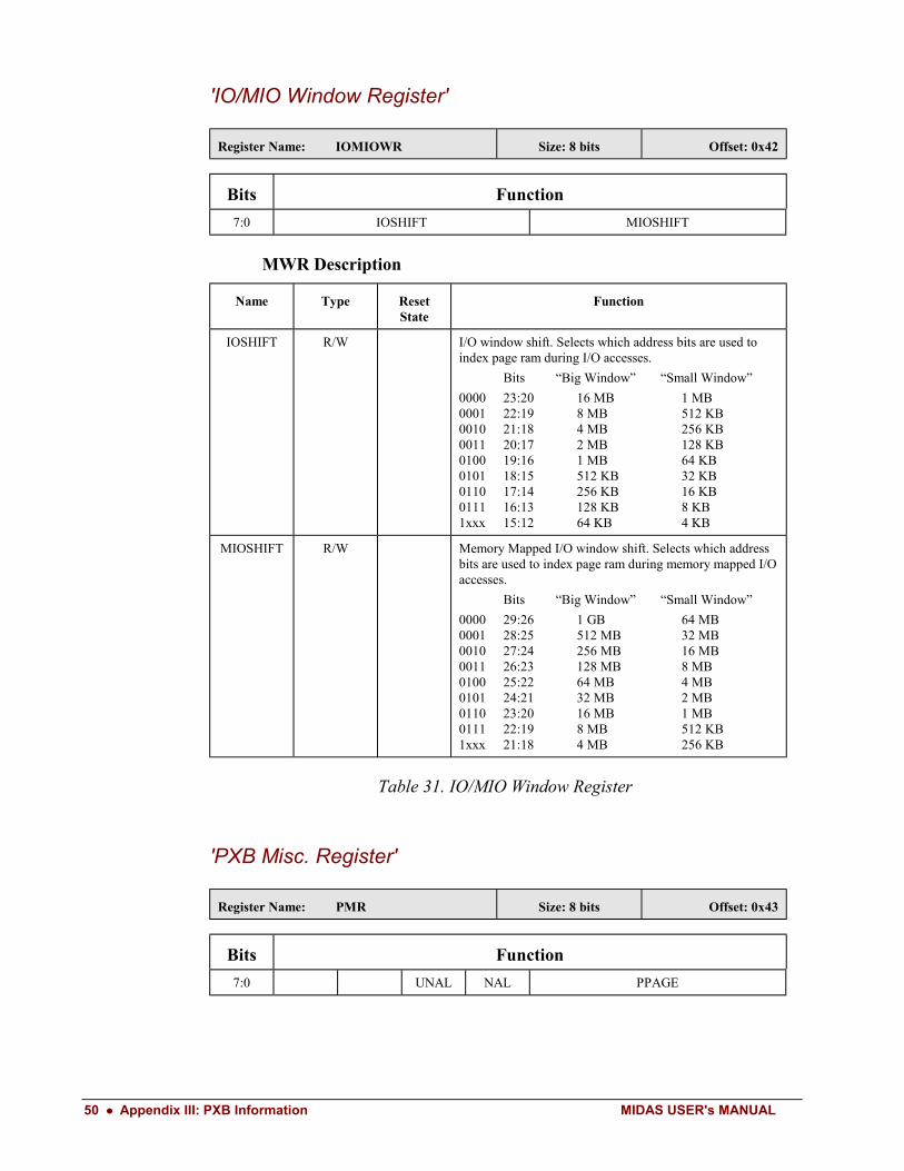
50 •••• Appendix III: PXB Information MIDAS USER's MANUAL
'IO/MIO Window Register'
Register Name: IOMIOWR Size: 8 bits Offset: 0x42
Bits Function
7:0 IOSHIFT MIOSHIFT
MWR Description
Name Type ResetState
Function
IOSHIFT R/W I/O window shift. Selects which address bits are used toindex page ram during I/O accesses.
Bits “Big Window” “Small Window”
0000 23:20 16 MB 1 MB0001 22:19 8 MB 512 KB0010 21:18 4 MB 256 KB0011 20:17 2 MB 128 KB0100 19:16 1 MB 64 KB0101 18:15 512 KB 32 KB0110 17:14 256 KB 16 KB0111 16:13 128 KB 8 KB1xxx 15:12 64 KB 4 KB
MIOSHIFT R/W Memory Mapped I/O window shift. Selects which addressbits are used to index page ram during memory mapped I/Oaccesses.
Bits “Big Window” “Small Window”
0000 29:26 1 GB 64 MB0001 28:25 512 MB 32 MB0010 27:24 256 MB 16 MB0011 26:23 128 MB 8 MB0100 25:22 64 MB 4 MB0101 24:21 32 MB 2 MB0110 23:20 16 MB 1 MB0111 22:19 8 MB 512 KB1xxx 21:18 4 MB 256 KB
Table 31. IO/MIO Window Register
'PXB Misc. Register'
Register Name: PMR Size: 8 bits Offset: 0x43
Bits Function
7:0 UNAL NAL PPAGE
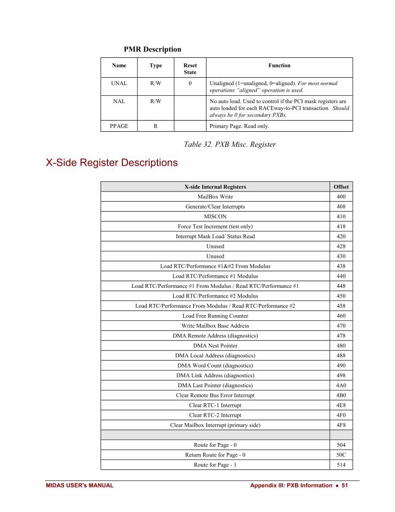
MIDAS USER's MANUAL Appendix III: PXB Information •••• 51
PMR Description
Name Type ResetState
Function
UNAL R/W 0 Unaligned (1=unaligned, 0=aligned). For most normaloperations “aligned” operation is used.
NAL R/W No auto load. Used to control if the PCI mask registers areauto loaded for each RACEway-to-PCI transaction. Shouldalways be 0 for secondary PXBs.
PPAGE R Primary Page. Read only.
Table 32. PXB Misc. Register
X-Side Register Descriptions
X-side Internal Registers Offset
MailBox Write 400
Generate/Clear Interrupts 408
MISCON 410
Force Test Increment (test only) 418
Interrupt Mask Load/ Status Read 420
Unused 428
Unused 430
Load RTC/Performance #1 From Modulus 438
Load RTC/Performance #1 Modulus 440
Load RTC/Performance #1 From Modulus / Read RTC/Performance #1 448
Load RTC/Performance #2 Modulus 450
Load RTC/Performance From Modulus / Read RTC/Performance #2 458
Load Free Running Counter 460
Write Mailbox Base Address 470
DMA Remote Address (diagnostics) 478
DMA Nest Pointer 480
DMA Local Address (diagnostics) 488
DMA Word Count (diagnostics) 490
DMA Link Address (diagnostics) 498
DMA Last Pointer (diagnostics) 4A0
Clear Remote Bus Error Interrupt 4B0
Clear RTC-1 Interrupt 4E8
Clear RTC-2 Interrupt 4F0
Clear Mailbox Interrupt (primary side) 4F8
Route for Page - 0 504
Return Route for Page - 0 50C
Route for Page - 1 514
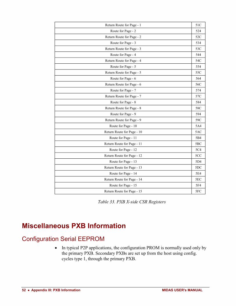
52 •••• Appendix III: PXB Information MIDAS USER's MANUAL
Return Route for Page - 1 51C
Route for Page - 2 524
Return Route for Page - 2 52C
Route for Page - 3 534
Return Route for Page - 3 53C
Route for Page - 4 544
Return Route for Page - 4 54C
Route for Page - 5 554
Return Route for Page - 5 55C
Route for Page - 6 564
Return Route for Page - 6 56C
Route for Page - 7 574
Return Route for Page - 7 57C
Route for Page - 8 584
Return Route for Page - 8 58C
Route for Page - 9 594
Return Route for Page - 9 59C
Route for Page - 10 5A4
Return Route for Page - 10 5AC
Route for Page - 11 5B4
Return Route for Page - 11 5BC
Route for Page - 12 5C4
Return Route for Page - 12 5CC
Route for Page - 13 5D4
Return Route for Page - 13 5DC
Route for Page - 14 5E4
Return Route for Page - 14 5EC
Route for Page - 15 5F4
Return Route for Page - 15 5FC
Table 33. PXB X-side CSR Registers
Miscellaneous PXB Information
Configuration Serial EEPROM• In typical P2P applications, the configuration PROM is normally used only by
the primary PXB. Secondary PXBs are set up from the host using config.cycles type 1, through the primary PXB.
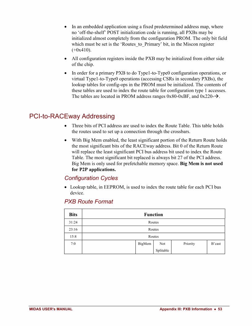
MIDAS USER's MANUAL Appendix III: PXB Information •••• 53
• In an embedded application using a fixed predetermined address map, whereno ‘off-the-shelf’ POST initialization code is running, all PXBs may beinitialized almost completely from the configuration PROM. The only bit fieldwhich must be set is the ‘Routes_to_Primary’ bit, in the Miscon register(+0x410).
• All configuration registers inside the PXB may be initialized from either sideof the chip.
• In order for a primary PXB to do Type1-to-Type0 configuration operations, orvirtual Type1-to-Type0 operations (accessing CSRs in secondary PXBs), thelookup tables for config-ops in the PROM must be initialized. The contents ofthese tables are used to index the route table for configuration type 1 accesses.The tables are located in PROM address ranges 0x80-0xBF, and 0x220- .
PCI-to-RACEway Addressing• Three bits of PCI address are used to index the Route Table. This table holds
the routes used to set up a connection through the crossbars.
• With Big Mem enabled, the least significant portion of the Return Route holdsthe most significant bits of the RACEway address. Bit 0 of the Return Routewill replace the least significant PCI bus address bit used to index the RouteTable. The most significant bit replaced is always bit 27 of the PCI address.Big Mem is only used for prefetchable memory space. Big Mem is not usedfor P2P applications.
Configuration Cycles
• Lookup table, in EEPROM, is used to index the route table for each PCI busdevice.
PXB Route Format
Bits Function
31:24 Routes
23:16 Routes
15:8 Routes
7:0 BigMem Not
Splitable
Priority B’cast
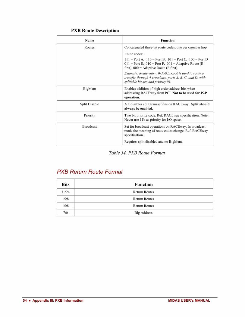
54 •••• Appendix III: PXB Information MIDAS USER's MANUAL
PXB Route Description
Name Function
Routes Concatenated three-bit route codes, one per crossbar hop.
Route codes:
111 = Port A, 110 = Port B, 101 = Port C, 100 = Port D011 = Port E, 010 = Port F, 001 = Adaptive Route (Efirst), 000 = Adaptive Route (F first).
Example: Route entry: 0xFACx.xxxA is used to route atransfer through 4 crossbars, ports A, B, C, and D, withsplitable bit set, and priority 01.
BigMem Enables addition of high order address bits whenaddressing RACEway from PCI. Not to be used for P2Poperation.
Split Disable A 1 disables split transactions on RACEway. Split shouldalways be enabled.
Priority Two bit priority code. Ref. RACEway specification. Note:Never use 11b as priority for I/O space.
Broadcast Set for broadcast operations on RACEway. In broadcastmode the meaning of route codes change. Ref. RACEwayspecification.
Requires split disabled and no BigMem.
Table 34. PXB Route Format
PXB Return Route Format
Bits Function
31:24 Return Routes
15:8 Return Routes
15:8 Return Routes
7:0 Big Address
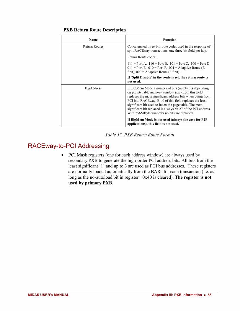
MIDAS USER's MANUAL Appendix III: PXB Information •••• 55
PXB Return Route Description
Name Function
Return Routes Concatenated three-bit route codes used in the response ofsplit RACEway transactions, one three-bit field per hop.
Return Route codes:
111 = Port A, 110 = Port B, 101 = Port C, 100 = Port D011 = Port E, 010 = Port F, 001 = Adaptive Route (Efirst), 000 = Adaptive Route (F first).
If ‘Split Disable’ in the route is set, the return route isnot used.
BigAddress In BigMem Mode a number of bits (number is dependingon prefetchable memory window size) from this fieldreplaces the most significant address bits when going fromPCI into RACEway. Bit 0 of this field replaces the leastsignificant bit used to index the page table. The mostsignificant bit replaced is always bit 27 of the PCI address.With 256MByte windows no bits are replaced.
If BigMem Mode is not used (always the case for P2Papplications), this field is not used.
Table 35. PXB Return Route Format
RACEway-to-PCI Addressing• PCI Mask registers (one for each address window) are always used by
secondary PXB to generate the high-order PCI address bits. All bits from theleast significant ‘1’ and up to 3 are used as PCI bus addresses. These registersare normally loaded automatically from the BARs for each transaction (i.e. aslong as the no-autoload bit in register +0x40 is cleared). The register is notused by primary PXB.
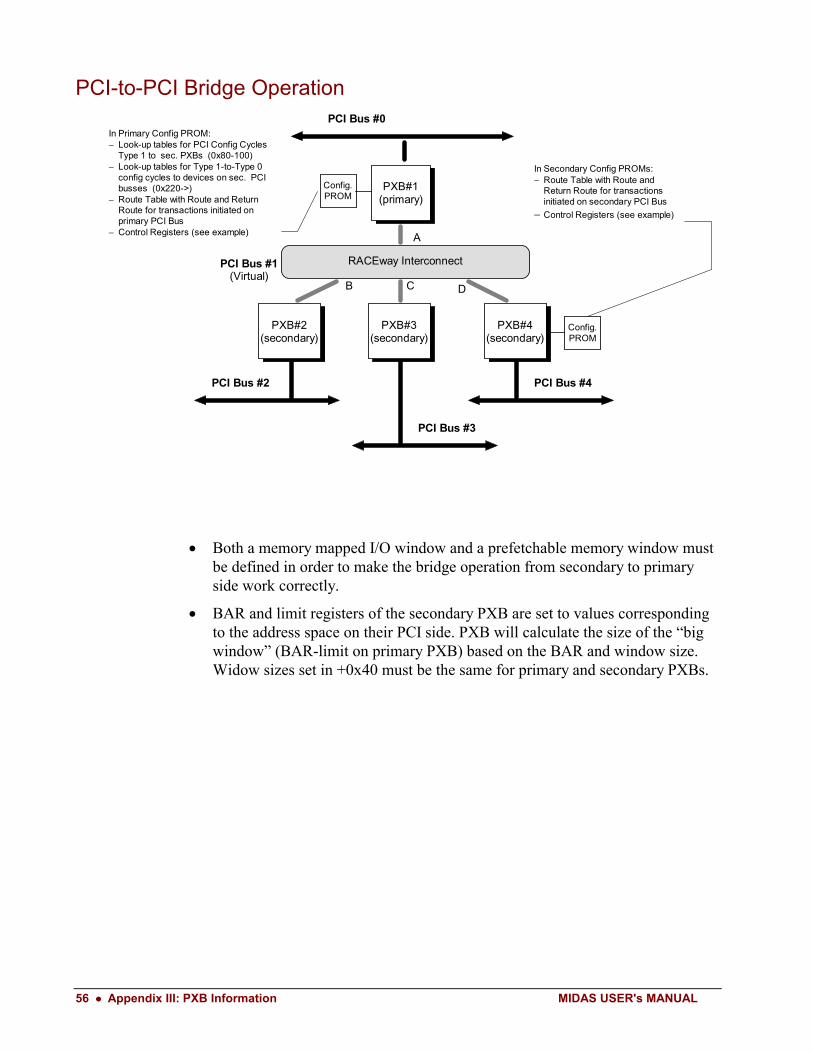
56 •••• Appendix III: PXB Information MIDAS USER's MANUAL
PCI-to-PCI Bridge Operation
PCI Bus #4PCI Bus #2
PXB#4(secondary)
PXB#3(secondary)
PXB#2(secondary)
Config.PROM
PXB#1(primary)
DC
A
B
PCI Bus #1(Virtual)
PCI Bus #0
RACEway Interconnect
PCI Bus #3
In Primary Config PROM:− Look-up tables for PCI Config Cycles
Type 1 to sec. PXBs (0x80-100)− Look-up tables for Type 1-to-Type 0
config cycles to devices on sec. PCIbusses (0x220->)
− Route Table with Route and ReturnRoute for transactions initiated onprimary PCI Bus
− Control Registers (see example)
Config.PROM
In Secondary Config PROMs:− Route Table with Route and
Return Route for transactionsinitiated on secondary PCI Bus
− Control Registers (see example)
• Both a memory mapped I/O window and a prefetchable memory window mustbe defined in order to make the bridge operation from secondary to primaryside work correctly.
• BAR and limit registers of the secondary PXB are set to values correspondingto the address space on their PCI side. PXB will calculate the size of the “bigwindow” (BAR-limit on primary PXB) based on the BAR and window size.Widow sizes set in +0x40 must be the same for primary and secondary PXBs.
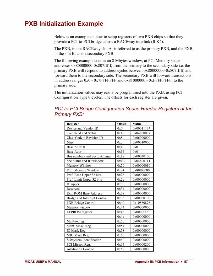
MIDAS USER's MANUAL Appendix III: PXB Information •••• 57
PXB Initialization Example
Below is an example on how to setup registers of two PXB chips so that theyprovide a PCI-to-PCI bridge across a RACEway interlink (ILK4).
The PXB, in the RACEway slot A, is referred to as the primary PXB, and the PXB,in the slot B, as the secondary PXB.
The following example creates an 8 Mbytes window, at PCI Memory spaceaddresses 0x80000000-0x807fffff, from the primary to the secondary side i.e. theprimary PXB will respond to address cycles between 0x80000000-0x807fffff, andforward them to the secondary side. The secondary PXB will forward transactionsin address ranges 0x0 - 0x7FFFFFFF and 0x81000000 - 0xFFFFFFFF, to theprimary side.
The initialization values may easily be programmed into the PXB, using PCIConfiguration Type 0 cycles. The offsets for each register are given.
PCI-to-PCI Bridge Configuration Space Header Registers of thePrimary PXB:
Register Offset ValueDevice and Vendor ID 0x0 0x00011134Command and Status 0x4 0x04800007Class Code + Revision ID 0x8 0x06000000Misc. 0xc 0x00010000Base Addr. 0 0x10 0x0Base Addr. 1 0x14 0x0Bus numbers and Sec.Lat.Timer 0x18 0x00030100Sec.Status and IO window 0x1C 0x04800111Memory Window 0x20 0x00000010Pref. Memory Window 0x24 0x80f08000Pref. Base Upper 32 bits 0x28 0x00000000Pref. Limit Upper 32 bits 0x2c 0x00000000IO upper 0x30 0x00000000Reserved 0x34 0x00000000Exp. ROM Base Address 0x38 0x00000000Bridge and Interrupt Control 0x3c 0x00000100PXB Bridge Control 0x40 0x10880826Memory window 0x44 0x00000000EEPROM register 0x48 0x0000f773. 0x4c 0x00000000Mailbox reg. 0x50 0x00000000Mem. Mask. Reg. 0x54 0x00000000IO Mask Reg. 0x58 0x00000000MIO Mask Reg. 0x5c 0x00000000Subsystem Identification 0x60 0x00000000PCI Miscon Reg. 0x64 0x00000200Arbitration Control 0x68 0x00000000
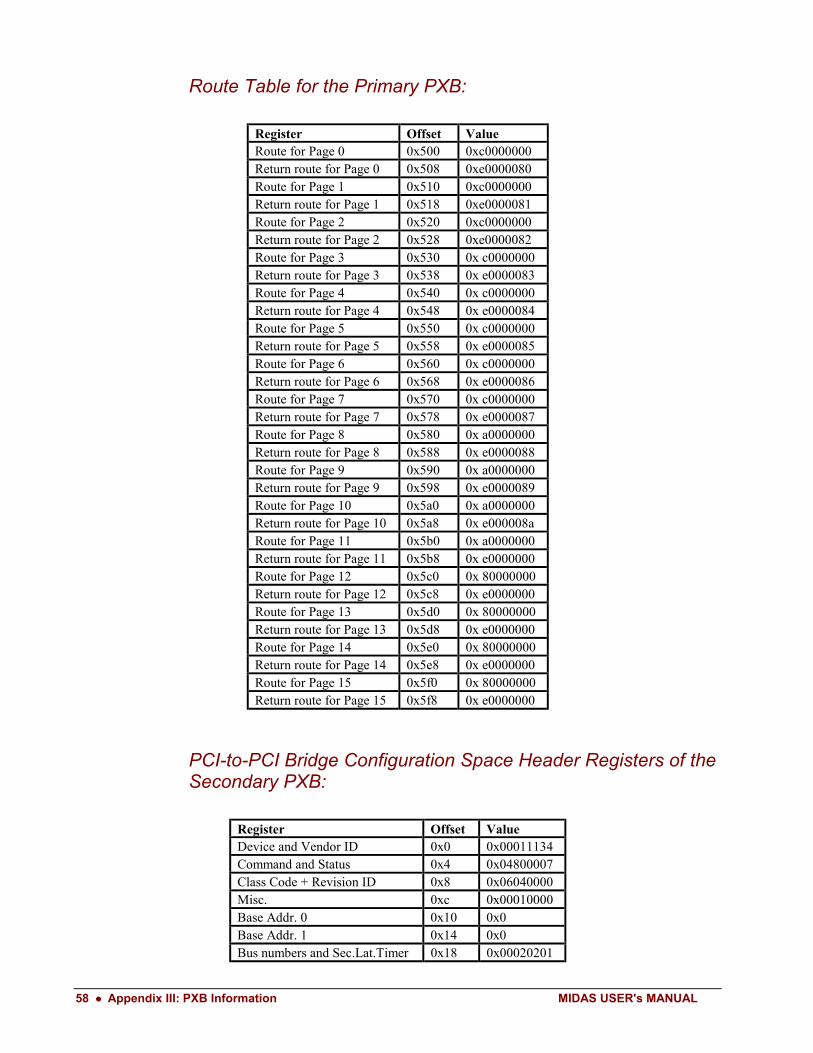
58 •••• Appendix III: PXB Information MIDAS USER's MANUAL
Route Table for the Primary PXB:
Register Offset ValueRoute for Page 0 0x500 0xc0000000Return route for Page 0 0x508 0xe0000080Route for Page 1 0x510 0xc0000000Return route for Page 1 0x518 0xe0000081Route for Page 2 0x520 0xc0000000Return route for Page 2 0x528 0xe0000082Route for Page 3 0x530 0x c0000000Return route for Page 3 0x538 0x e0000083Route for Page 4 0x540 0x c0000000Return route for Page 4 0x548 0x e0000084Route for Page 5 0x550 0x c0000000Return route for Page 5 0x558 0x e0000085Route for Page 6 0x560 0x c0000000Return route for Page 6 0x568 0x e0000086Route for Page 7 0x570 0x c0000000Return route for Page 7 0x578 0x e0000087Route for Page 8 0x580 0x a0000000Return route for Page 8 0x588 0x e0000088Route for Page 9 0x590 0x a0000000Return route for Page 9 0x598 0x e0000089Route for Page 10 0x5a0 0x a0000000Return route for Page 10 0x5a8 0x e000008aRoute for Page 11 0x5b0 0x a0000000Return route for Page 11 0x5b8 0x e0000000Route for Page 12 0x5c0 0x 80000000Return route for Page 12 0x5c8 0x e0000000Route for Page 13 0x5d0 0x 80000000Return route for Page 13 0x5d8 0x e0000000Route for Page 14 0x5e0 0x 80000000Return route for Page 14 0x5e8 0x e0000000Route for Page 15 0x5f0 0x 80000000Return route for Page 15 0x5f8 0x e0000000
PCI-to-PCI Bridge Configuration Space Header Registers of theSecondary PXB:
Register Offset ValueDevice and Vendor ID 0x0 0x00011134Command and Status 0x4 0x04800007Class Code + Revision ID 0x8 0x06040000Misc. 0xc 0x00010000Base Addr. 0 0x10 0x0Base Addr. 1 0x14 0x0Bus numbers and Sec.Lat.Timer 0x18 0x00020201
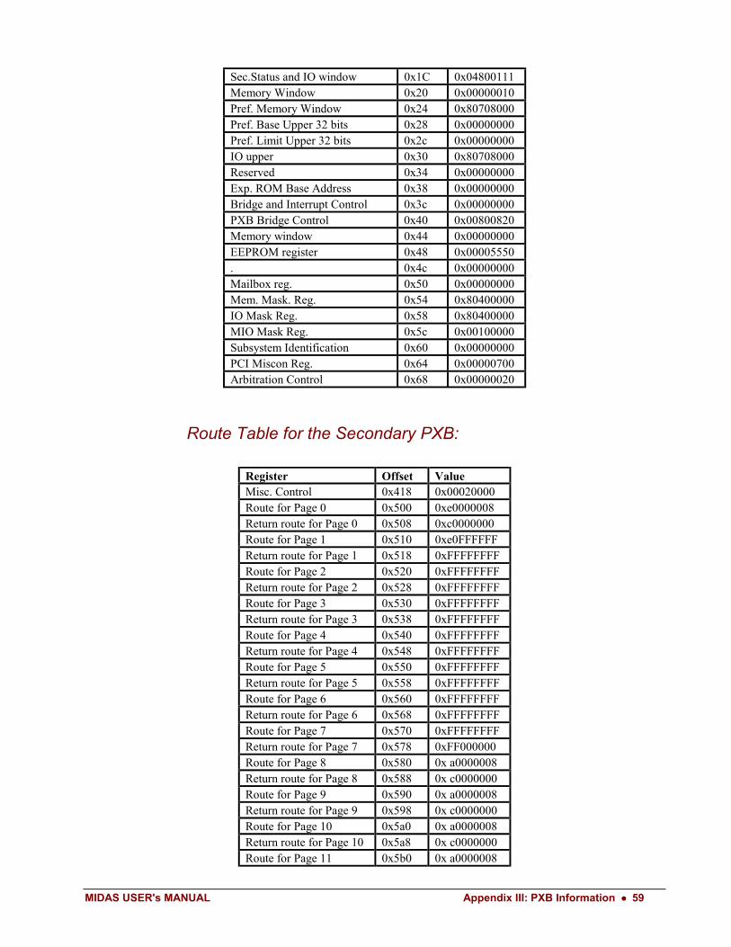
MIDAS USER's MANUAL Appendix III: PXB Information •••• 59
Sec.Status and IO window 0x1C 0x04800111Memory Window 0x20 0x00000010Pref. Memory Window 0x24 0x80708000Pref. Base Upper 32 bits 0x28 0x00000000Pref. Limit Upper 32 bits 0x2c 0x00000000IO upper 0x30 0x80708000Reserved 0x34 0x00000000Exp. ROM Base Address 0x38 0x00000000Bridge and Interrupt Control 0x3c 0x00000000PXB Bridge Control 0x40 0x00800820Memory window 0x44 0x00000000EEPROM register 0x48 0x00005550. 0x4c 0x00000000Mailbox reg. 0x50 0x00000000Mem. Mask. Reg. 0x54 0x80400000IO Mask Reg. 0x58 0x80400000MIO Mask Reg. 0x5c 0x00100000Subsystem Identification 0x60 0x00000000PCI Miscon Reg. 0x64 0x00000700Arbitration Control 0x68 0x00000020
Route Table for the Secondary PXB:
Register Offset ValueMisc. Control 0x418 0x00020000Route for Page 0 0x500 0xe0000008Return route for Page 0 0x508 0xc0000000Route for Page 1 0x510 0xe0FFFFFFReturn route for Page 1 0x518 0xFFFFFFFFRoute for Page 2 0x520 0xFFFFFFFFReturn route for Page 2 0x528 0xFFFFFFFFRoute for Page 3 0x530 0xFFFFFFFFReturn route for Page 3 0x538 0xFFFFFFFFRoute for Page 4 0x540 0xFFFFFFFFReturn route for Page 4 0x548 0xFFFFFFFFRoute for Page 5 0x550 0xFFFFFFFFReturn route for Page 5 0x558 0xFFFFFFFFRoute for Page 6 0x560 0xFFFFFFFFReturn route for Page 6 0x568 0xFFFFFFFFRoute for Page 7 0x570 0xFFFFFFFFReturn route for Page 7 0x578 0xFF000000Route for Page 8 0x580 0x a0000008Return route for Page 8 0x588 0x c0000000Route for Page 9 0x590 0x a0000008Return route for Page 9 0x598 0x c0000000Route for Page 10 0x5a0 0x a0000008Return route for Page 10 0x5a8 0x c0000000Route for Page 11 0x5b0 0x a0000008
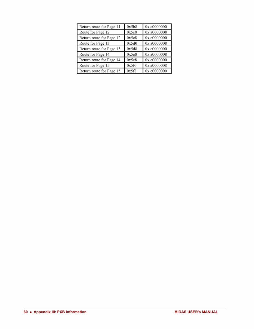
60 •••• Appendix III: PXB Information MIDAS USER's MANUAL
Return route for Page 11 0x5b8 0x c0000000Route for Page 12 0x5c0 0x a0000008Return route for Page 12 0x5c8 0x c0000000Route for Page 13 0x5d0 0x a0000008Return route for Page 13 0x5d8 0x c0000000Route for Page 14 0x5e0 0x a0000008Return route for Page 14 0x5e8 0x c0000000Route for Page 15 0x5f0 0x a0000008Return route for Page 15 0x5f8 0x c0000000
MIDAS USER's MANUAL Appendix IV: •••• 61
Appendix IV:
List of TablesTable 1. Power Consumption ............................................................................................................................................ 12Table 2. 'Universe II' Power-Up Options........................................................................................................................... 19Table 3. MIDAS Configuration ROM............................................................................................................................... 20Table 4. VRAI Base Address Definition ........................................................................................................................... 22Table 5. Secondary PCI Bus.............................................................................................................................................. 26Table 6. Primary PCI Bus - Arbiter: RD#1 ....................................................................................................................... 26Table 7. Primary PCI Bus - Arbiter: PXB ......................................................................................................................... 27Table 8. IDSEL Assignments for Primary PCI Bus........................................................................................................... 27Table 9. IDSEL Assignments for Secondary PCI Bus....................................................................................................... 28Table 10. Interrupt Mode Selection................................................................................................................................... 30Table 11. VME_RAI Setup. .............................................................................................................................................. 38Table 12. VME Slave Image 0 - Setup ............................................................................................................................ 38Table 13. VME Slave Image 1 - Setup. ........................................................................................................................... 39Table 14. VME Slave Image 2 - Setup. ........................................................................................................................... 39Table 15. Initialization Sequence for VMEbus Slave Image Config. Example. ................................................................ 40Table 16. PCI Slave Image 0 Setup. .................................................................................................................................. 42Table 17. PCI Slave Image 1 Setup. .................................................................................................................................. 42Table 18. PCI Slave Image 2 Setup. .................................................................................................................................. 42Table 19. Initialization Sequence for PCI Slave Image Config. Example. ........................................................................ 43Table 20. PXB P-side CSR Registers................................................................................................................................ 44Table 21. PCI Command Register ..................................................................................................................................... 45Table 22. PCI Status Register............................................................................................................................................ 45Table 23. Secondary Status Register ................................................................................................................................. 46Table 24. Memory Mapped I/O Base Address Register .................................................................................................... 46Table 25. Memory Mapped I/O Limit Address Register ................................................................................................... 47Table 26. Prefetchable Memory Base Address Register.................................................................................................... 47Table 27. Prefetchable Memory Limit Address Register................................................................................................... 48Table 28. Bridge Control Register..................................................................................................................................... 48Table 29. PXB Bridge Control Register............................................................................................................................ 49Table 30. Memory Window Register ................................................................................................................................ 49Table 31. IO/MIO Window Register ................................................................................................................................. 50Table 32. PXB Misc. Register........................................................................................................................................... 51Table 33. PXB X-side CSR Registers ............................................................................................................................... 52Table 34. PXB Route Format ............................................................................................................................................ 54Table 35. PXB Return Route Format ................................................................................................................................ 55
62 •••• Appendix IV: MIDAS USER's MANUAL
List of FiguresFigure 1. MIDAS-220/250 Block Diagram..........................................................................................................................3Figure 2. MIDAS-120/150 Block Diagram..........................................................................................................................4Figure 3. i960®RD Data Flow..............................................................................................................................................5Figure 4 PCI-VME bridge functional diagram.....................................................................................................................6Figure 5. MIDAS Board Layout (No model has all parts mounted.) ...................................................................................8Figure 6. Steps 2&3: Mount PMC modules on the MEZZ-x50 and MIDAS-x20 boards. .................................................10Figure 7. Step 4: Mount the MEZZ-x50 with PMC modules on the MIDAS-x20 board. ..................................................11Figure 8. i960®RD with External Devices..........................................................................................................................14Figure 9. Local Memory Address Space ............................................................................................................................15Figure 10. FLASH Boot Address .......................................................................................................................................17Figure 11. Pin definition for the RS232 female connector mounted on the front panel .....................................................17Figure 12. Connection of two i960®RDs on MIDAS-220..................................................................................................18Figure 13. DIP Switch Details. (Shown switch value: 0x81) .............................................................................................22Figure 14. Configuration Example for VMEbus Slave Images ..........................................................................................37Figure 15. Configuration Example for PCI Slave Images ..................................................................................................41