Embed Size (px)
Citation preview

Linköping Studies in Science and Technology
Dissertation No. 1265
M i c r o w a v e P o w e r D e v i c e s a n d A m p l i f i e r s
f o r R a d a r s a n d C o m m u n i c a t i o n S y s t e m s
S h e r A z a m
Semiconductor Materials Division
Department of Physics, Chemistry and Biology
Linköpings Universitet, SE-581 83 Linköping, Sweden
Linköping 2009

Cover: A block diagram from top to bottom represents the goal of our device and power amplifier research work. On top are structures of microwave power transistors used in our TCAD simulations. In the middle is a simplified block diagram of power amplifier and in the bottom is a block diagram of an active phased array system.
Copyright © 2009 by Sher Azam
ISBN: 978-91-7393-576-0
ISSN: 0345-7524
http://urn.kb.se/resolve?urn=urn:nbn:se:liu:diva-19267
Printed by Liutryck, Linköping University,
Linköping, Sweden
June, 2009

To my Parents, family and all those who pray for the completion of this thesis.


ACKNOWLEDGMENTS
All praise is due to our God (ALLAH) who enabled me to do this research work. I know
that being Physicist it was not an easy job to become a circuit designer as well. But interest,
determination and trust in God can make every thing possible. Of course, I could not have done
this work without the help and contributions of other people that I am grateful to;
• I’m deeply indebted to my supervisor, Associate Prof. Qamar ul Wahab and co-
supervisor Prof. Erik Janzén, Head of Semiconductor group at IFM, for guidance and
encouragement during the research work. They introduced me to the most experienced
and pronounced researchers of professional world, Prof. Christer Svensson former head
of electronic device group, Department of Electrical Engineering (ISY) and Tech. Lic.
Rolf Jonsson, Microwave Technology group at Swedish Defense Research Agency
(FOI). I am thankful to them for useful recommendations, excellent guidance and giving
me fantastic feedback.
• I acknowledge Swedish Defense Research Agency (FOI) Linkoping for providing their
facilities of fabrication and characterization of power amplifiers and other technical
support in this work.
• Stig Leijon at Swedish Defense Research Agency (FOI), for manufacturing amplifiers
and help with the development of the measurement fixtures.
• I am thankful to Atila Alvandpour, Head of electronics devices group, Department of
Electrical Engineering (ISY) for providing me software and other facilities at ISY.
• M.Sc. Jonas Fritzen (ISY), I enjoyed fruitful discussions with him in the last couple of
months during our class E switching power amplifier designing and fabrication work.
• Research Engineer Arta Alvandpour (ISY) for solving ADS software related problems.
• I also acknowledge Infineon Technologies at Kista, Stockholm for providing Si-LDMOS
structure and technical support.
• My friends Ahsan ullah Kashif and Asad Abbas for TCAD software related help in the
initial stage of my simulation work.
• Prof. Bo Monemar, Prof. Per-Olof, Prof. Arina Buyanova for excellent teaching, which
help me to understand Semiconductor Physics and technology in-depth and Prof. Leif
Johansson for help. Our group secretary Eva Wibom for the help in administrative work.
• My colleagues at Material Science Division. I am thankful to Dr. Aamir Karim for
explaining device growth practically during growth steps in the lab, its characterization
1

and related equipments. I would also acknowledge M.Sc. Franziska for training on metal
contact growth, Dr. Rafal Chuzraski for training on CV & IV characteristics and wire
bonding, Dr. Henrik for training on wafer and sample cleaning, Dr. Ming for training on
lithography steps in clean room class 100. I am also thankful to the teaching staff and lab
responsible of different courses; (IFM and ISY at Linkoping Campus and microwave
group ITN at Norkoping Campus) I attended during my PhD studies. They have a great
contribution in my scientific development and this research work.
• My friend Naveed Ahsan for excellent supervision during VLSI chip designing,
fabrication and testing course, which will be helpful for possible MMIC designing and
implementation work in the future.
• I am thankful to my senior colleagues in Pakistan, especially Muhammad Imran, for
having confidence and faith in me. Due to my interest in the circuit designing he always
encouraged me and facilitated me with required literature, managed Advance Design
System software training by experts from Agilent Technologies Singapore. All my other
colleagues and Nauman Akhtar for help in the initial stage of learning ADS.
• Apart from studies, thanks to Dr. Tanveer Muftee, A. Kashif, Saad Rehman, G. Mehdi,
Riaz Muhammad, Ijaz Akhtar, Jawad ul Hassan, Rashad Ramzan, Rizwan Asghar,
Abdul Qahar, Haji Daud and all those friends and their families who helped us during
our stay, which gave us homelike feelings. Thanks to all members of biweekly
gatherings which were the real motivating factors and played important role in my
intellectual development. I also learned a lot from PSA activities especially on
management side. It has definitely improved my management skills.
• My deep gratitude is due, to my parents and other family members, for their continuous
guidance, encouragement, support, and prayers during my life. I am grateful to my
brother Abdullah Mir, for the unconditional support throughout my education carrier.
• Thanks are due, to my wife Shumaila Rehman, for her patience, help, and being away
from her family for several years during my study. To my sons, Muhammad
Fakhar e Azam, Muhammad Faizan Azam and Muhammad Shawaiz Azam for giving
me happiness. My love is always for you.
Sher Azam June, 2009,
Linköping, Sweden
2

ABSTRACT
SiC MESFETs and GaN HEMTs posses an enormous potential in power amplifiers at
microwave frequencies due to their wide bandgap features of high electric field strength, high
electron saturation velocity and high operating temperature. The high power density combined
with the comparably high impedance attainable by these devices also offers new possibilities for
wideband power microwave systems. Similarly Si-LDMOS being low cost and lonely silicon
based RF power transistor has great contributions especially in the communication sector.
The focus of this thesis work is both device study and their application in different
classes of power amplifiers. In the first part of our research work, we studied the performance
of transistors in device simulation using physical transistor structure in Technology Computer
Aided Design (TCAD). A comparison between the physical simulations and measured device
characteristics has been carried out. We optimized GaN HEMT, Si-LDMOS and enhanced
version of our previously fabricated and tested SiC MESFET transistor for enhanced RF and DC
characteristics. For large signal AC performance we further extended the computational load pull
(CLP) simulation technique to study the switching response of the power transistors. The beauty
of our techniques is that, we need no lumped or distributive matching networks to study active
device behavior in almost all major classes of power amplifiers. Using these techniques, we
studied class A, AB, pulse input class-C and class-F switching response of SiC MESFET. We
obtained maximum PAE of 78.3 % with power density of 2.5 W/mm for class C and 84 % for
class F power amplifier at 500 MHz. The Si-LDMOS has a vital role and is a strong competitor
to wideband gap semiconductor technology in communication sector. We also studied Si-
LDMOS (transistor structure provided by Infineon Technologies at Kista, Stockholm) for
improved DC and RF performance. The interface charges between the oxide and RESURF
region are used not only to improve DC drain current and RF power, gain & efficiency but also
enhance its operating frequency up to 4 GHz.
In the second part of our research work, six single stage (using single transistor)
power amplifiers have been designed, fabricated and characterized in three phases for
applications in communications, Phased Array Radars and EW systems. In the first phase, two
class AB power amplifiers are designed and fabricated. The first PA (26 W) is designed and
fabricated at 200-500 MHz using SiC MESFET. Typical results for this PA at 60 V drain bias at
500 MHz are, 24.9 dB of power gain, 44.15 dBm output power (26 W) and 66 % PAE. The
second PA is designed at 30-100 MHz using SiC MESFET. At 60 V drain bias Pmax is 46.7 dBm
(~47 W) with a power gain of 21 dB.
3

In the second phase, for performance comparison, three broadband class AB power
amplifiers are designed and fabricated at 0.7-1.8 GHz using SiC MESFET and two different
GaN HEMT technologies (GaN HEMT on SiC and GaN HEMT on Silicon substrate). The
measured maximum output power for the SiC MESFET amplifier at a drain bias of Vd= 66 V at
700 MHz the Pmax was 42.2 dBm (~16.6 W) with a PAE of 34.4 %. The results for GaN HEMT
on SiC amplifier are; maximum output power at Vd = 48 V is 40 dBm (~10 W), with a PAE of
34 % and a power gain above 10 dB. The maximum output power for GaN HEMT on Si
amplifier is 42.5 dBm (~18 W) with a maximum PAE of 39 % and a gain of 19.5 dB.
In the third phase, a high power single stage class E power amplifier is implemented
with lumped elements at 0.89-1.02 GHz using Silicon GaN HEMT as an active device. The
maximum drain efficiency (DE) and PAE of 67 and 65 % respectively is obtained with a
maximum output power of 42.2 dBm (~ 17 W) and a maximum power gain of 15 dB.
4

Preface
This thesis comprises of two sections. The first section contains introduction, importance
and response of wide bandgap (SiC and GaN) and conventional Si-LDMOS transistors in power
amplifiers and some important results of our power amplifiers. The second section presents
results compiled in nine publications. This thesis is presented as partial fulfillment of the
requirements for the degree of Doctor of Philosophy, of Linköping University. The work
described in the thesis has been carried out at Semiconductor Physics Division, Department of
Physics (IFM) and Department of Electrical Engineering (ISY) at Linköping University and at
the Department of Microwave Technology, Swedish Defense Research Agency (FOI) between
September 2005 and September 2009.
List of appended publications
Paper 1: S. Azam, C. Svensson and Q. Wahab: “Pulse Input Class-C Power Amplifier
Response of SiC MESFET using Physical Transistor Structure in TCAD”, J. of Solid State
Electronics, Vol. 52/5, 2008, pp 740-744.
Paper 2: S. Azam, R. Jonsson, C. Svensson and Q. Wahab: “High Power, High Efficiency
SiC Power Amplifier for Phased Array Radar and VHF Applications”, submitted manuscript
in 2009.
Paper 3: S. Azam, R. Jonsson, Q. Wahab: “Single-stage, High Efficiency, 26-Watt power
Amplifier using SiC LE-MESFET”, IEEE Asia Pacific Microwave Conf. (APMC),
YokoHama (Japan), pp. 441–444, December 2006.
Paper 4: S. Azam, R. Jonsson, C. Svensson and Q. Wahab: “Broadband Power Amplifier
Performance of SiC MESFET and Cost Effective SiGaN HEMT”, submitted manuscript in
2009.
Paper 5: S. Azam, R. Jonsson and Q. Wahab: “Designing, Fabrication and
Characterization of Power Amplifiers Based on 10-Watt SiC MESFET & GaN HEMT at
Microwave Frequencies”, Proceedings of IEEE 38th European Microwave Conference,
October 10-15, 2008. Pages: 444-447 Amsterdam, the Netherlands.
5

Paper 6: S. Azam, R. Jonsson, J. Fritzin, A. Alvandpour and Q. Wahab: “High Power,
Single Stage SiGaN HEMT Class E Power Amplifier at GHz Frequencies”, submitted
manuscript in 2009.
Paper 7: S. Azam, C. Svensson and Q. Wahab: “A New Load Pull TCAD Simulation
Technique for Class D, E & F Switching Characteristics of Transistors”, submitted
manuscript in 2009.
Paper 8: A. Kashif, T. Johansson, C. Svensson, S. Azam, T. Arnborg and Q. Wahab:
“Influence of interface state charges on RF performance of LDMOS transistor”, Journal of
Solid State Electronics, Vol. 52/7, 2008, pp 1099-1105.
Paper 9: S. Azam, R. Jonsson, C. Svensson and Q. Wahab: “Comparison of Two GaN
Transistors Technology in Broadband Power Amplifiers”, submitted manuscript in 2009.
RELATED PAPERS NOT INCLUDED IN THE THESIS
[1] SHER AZAM: “Wide Bandgap Semiconductor (SiC & GaN) Power Amplifiers in
Different Classes”, Licentiate Tech. Thesis, Linköping University 2008, LIU-TEK-LIC-
2008:32.
[2] S. Azam, C. Svensson and Q. Wahab: “Performance Limitations of SiC MESFET in Class-
A Power Amplifier” submitted manuscript in 2009.
[3] S. Azam, C. Svensson and Q. Wahab: “Pulse Width and Amplitude Modulation Effects on
the Switching Response of RF Power Transistor” submitted manuscript in 2009.
[4] Sher Azam, C. Svensson and Q. Wahab “Designing of High Efficiency Power Amplifier
Based on Physical Model of SiC MESFET in TCAD.” IEEE International Bhurban
Conference on Applied Sciences & Technology Islamabad, Pakistan, 8th-11th January,
2007, pp. 40-43.
[5] S. Azam, R. Jonsson, E. Janzen and Q. Wahab: “Performance of SiC Microwave
Transistors in Power Amplifiers”, Proceedings of MRS 2008 conference, San Francisco,
USA, March 24-28, 2008. Vol. 1069, 1069-D10-05
[6] A. Kashif, S. Azam, C. Svensson and Q. Wahab, “Flexible Power Amplifiers Designing
from Device to Circuit Level by Computational Load-Pull Simulation Technique in
6

TCAD”, ECS Transactions, 14 (1) 233-239 (2008) 10.1149/1.2956037 © The
Electrochemical Society.
[7] Sher Azam, R. Jonsson and Q. Wahab: “The Limiting Frontiers of Maximum DC Voltage
at the Drain of SiC Microwave Power Transistors in Case of Class-A Power Amplifier.”,
IEEE ISDRS 2007 conference, USA.
[8] S. Azam, R. Jonsson and Q. Wahab, “SINGLE STAGE, 47 W, CLASS-AB POWER
AMPLIFIER USING WBG SIC TRANSISTOR”, presented at 32nd Workshop on
Compound Semiconductor Devices and Integrated Circuits, WOCSDICE 2008, Leuven
(Belgium) May 18-21, 2008.
[9] A. Kashif, Christer Svensson, Sher Azam, and Qamr-ul Wahab, “A Non-Linear TCAD
Large Signal Model to Enhance the Linearity of Transistor”, IEEE ISDRS 2007
conference, USA
[10] Sher Azam, R. Jonsson and Q. Wahab, “Different Classes (A, AB, C & D) of Power
Amplifiers using SiC MESFET ”, Proc. of IEEE Gigahertz2008 conference, Sweden.
INVITED BOOK CHAPTERS
[1] Azam S. and Wahab Q.: GaN and SiC Based High Frequency Power Amplifiers. In
Microelectronics: Micro and Nano-Electronics and Photonics. New Delhi; Daya Publishing
House, 2009, (In Press)”
[2] S. Azam, R. Jonsson and Q. Wahab, “The present and future trends in High Power
Microwave and Millimeter Wave Technologies” IN-TECH Publishers, Kirchengasse 43/3
A-1070 Vienna, Austria, EU. Expected October 2009
7

LIST OF FIGURES
Fig. 1.1: A block diagram of TCAD simulation environment.
Fig. 1.2: DC-IV characteristics of our SiC MESFET.
Fig. 1.3: Schematic of our MESFET structure. In large transistors (for high Power),
multiple gates are combined to increase gate width.
Fig. 1.4: DC IV characteristics of our GaN HEMT.
Fig. 1.5: Schematic diagram of GaN/AlGaN HEMT structure.
Fig. 1.6: Structure and doping profile of the Infineon LDMOS transistor.
Fig. 1.7: Comparison of DC-IV characteristics of LDMOS structures with (solid lines) and
without excess interface state charges (dotted lines) at the RESURF region.
Fig. 1.8: A block diagram of wideband multifunction active phased array system.
Fig. 2.1: Block diagram of an amplifier.
Fig. 2.2: Typical classes of power amplifiers on the basis of gate biasing.
Fig. 2.3: The gain equalization (i.e., flat gain response) by introducing high attenuation at
low frequencies and low attenuation at high frequencies.
Fig. 2.4: POUT vs PIN, 1 dB compression point
Fig. 2.5: Schematic representation of two-tone intermodulation distortion
Fig. 3.1: A schematic of the fabricated power amplifier at 30-100 MHz
Fig. 3.2 RF power measurements at Vg = -8.5 V and Vd = 50 V at different frequencies.
Fig. 3.3: Measured results of gain, P1dB, Pmax and PAE at P1dB versus frequency at 60 V.
Fig. 3.4: Measured results of gain, Pmax and PAE versus frequency at 48 V drain bias.
Fig. 3.5: Two tone test results for SiC MESFET PA at 1 GHz, a tone spacing of 4 MHz.
Fig. 3.6: A schematic of the fabricated GaN on SiC power amplifier PA2 at 0.7-1.8 GHz
Fig. 3.7: Power measurement results at Vd = 48 V at three different frequencies for PA2
Fig. 3.8: A picture of the fabricated GaN on Si amplifier PA3
Fig. 3.9: Power measurement results at Vd = 28 V at five different frequencies for PA3
Fig. 3.10: Schematic of the large signal simulation technique for Class-C response.
Fig. 3.11: Pulse input Class-C Load lines at 0.5, 1, 2 & 3 GHz.
Fig. 3.12: A Schematic of the large signal TCAD simulation technique for Class-D, E & F
switching characteristics of devices.
8

LIST OF TABLES
Table 1.1: Material parameters of SiC and GaN compared to GaAs and Si.
Table 3.1: A Summary of class F power amplifier results at 500 MHz.
9

10

TABLE OF CONTENTS
ACKNOWLEDGEMENT 1
ABSTRACT 3
PREFACE 5
PAPERS INCLUDED IN THE THESIS 5
RELATED PAPERS NOT INCLUDED IN THE THESIS 6
INVITED BOOK CHAPTERS 7
LIST OF FIGURES 8
LIST OF TABLES 9
TABLE OF CONTENTS 11
CHAPTER 1: INTRODUCTION 15
1. Motivation 15
1.1 Computer Aided Simulations 18
1.2 Brief Historical background of Technology CAD (TCAD) 19
1.2.1 GENESISe 20
1.2.2 MDRAW 20
1.2.3 DESSIS 20
1.2.4 INSPECT 21
1.2.5 Tec plot 22
1.3 Fast Fourier Transform (FFT) in MATLAB 22
1.4 SiC MESFET 22
1.5 GaN HEMT 24
1.6 Silicon Lateral Diffused MOS (Si-LDMOS) FET 26
11

1.7 Phased Array System 28
CHAPTER 2: POWER AMPLIFIERS 31
2. Power Amplifier 31
2.1 Power Amplifier Classes 31
2.1.1 Class A 32
2.1.2 Class B 32
2.1.3 Class AB 33
2.1.4 Class C 33
2.1.5 Class D 33
2.1.6 Class E 33
2.1.7 Class F 34
2.1.8 Other High-Efficiency PA Classes 34
2.2 Broadband Amplifier 34
2.3 Power Amplifier Design Considerations 35
2.3.1 Output Power 36
2.3.2 Power Gain 36
2.3.3 Efficiency 36
2.3.3.1 Drain Efficiency (DE) 36
2.3.3.2 Power-Added Efficiency (PAE) 36
2.3.3.3 Over all Efficiency (OAE) 37
2.3.4 Stability 37
2.3.5 Linearity 37
2.3.5.1 1 dB gain compression (P1dB) 38
2.3.5.2 Input and Output Intercept point (IIP3 & OIP3) 39
2.3.5.3 Intermodulation Distortion 39
2.4 Performance of SiC Transistors in Power Amplifiers 40
12

2.5 Performance of GaN Transistors in Power Amplifiers 42
2.6 Performance of Si-LDMOS Transistors in Power Amplifiers 45
CHAPTER 3: SIMULATION AND MEASUREMENT RESULTS 47
3.1 Measured Results for PA at VHF frequencies (30-90 MHz) 47
3.2 Measured Results for PA at UHF frequencies (200-500 MHz) 48
3.3 Performance Comparison of Three different Technology Transistors in
Broadband Power Amplifiers (0.7-1.8 GHz) 49
3.3.1 Measured Results for SiC MESFET amplifier PA1 49
3.3.2 Measured Results for GaN on SiC amplifier PA2 50
3.3.3 Measured Results for GaN on Si amplifier PA3 52
3.4 Large Signal Computational Load pull (CLP) Simulation Techniques 53
3.4.1 CLP Technique for Class-A, B & AB power amplifier 53
3.4.2 CLP Technique for Class-C power amplifier 54
3.4.3 CLP Technique for Class-D, E & F power amplifier 55
CHAPTER 4: CONCLUSIONS 57
References 59
PAPERS 67
Paper 1
Paper 2
Paper 3
Paper 4
Paper 5
Paper 6
Paper 7
Paper 8
Paper 9
13

14
CHAPTER 1
INTRODUCTION
1. Motivation
GaAs-based power devices have been very reliable workhorses at high frequencies
especially in the microwave spectrum. However, their power performance has already been
pushed close to the theoretical limit [1]. Similarly, the fundamental physical limitations of Si
operation at higher temperature and powers are the strongest motivations for utilizing wide
bandgap (WBG) semiconductors such as SiC and GaN for these applications. Future phase array
radars, wireless communication market and other traditional military applications, require
demanding performance of microwave transistors. In several applications, as well as in radar and
military systems, the development of circuits and sub-systems with broadband capabilities is
always demanding. From transmitter point of view the bottleneck, and the critical key factor, is
the development of high performance PA. The latter, in fact, deeply influence the overall system
features in terms of bandwidth, output power, efficiency, working temperature etc. So far,
distributed approaches have often been proposed and investigated to design broadband
amplifiers [2].
Next generation cell phones require wider bandwidth and improved efficiency. The
development of satellite communications and TV broadcasting requires amplifiers operating at
higher frequencies and deliver high RF power, in order to reduce the size of antenna. The RF
power amplifier is consuming and dissipating the major portion of available power in these new
wireless communication systems. To extend battery life in mobile units, and reduce operating
costs of base stations, new amplifiers have to be developed to replace the traditionally
inefficient, old designs currently in use. Base station amplifiers of today employ many complex
techniques to meet linearity requirement, accompanying low efficiencies. Handset power
amplifiers also suffer greatly with efficiency problem, often more critical than those for base
stations.
There are several applications which need high power at high frequencies together with
efficiency and linearity. This high power and high efficiency applications require transistors with
high breakdown voltage, high electron velocity and high thermal conductivity. For this purpose,
transistors based on wide bandgap semiconductors such as GaN and SiC are preferable choices
15

[3]. A summary of the important parameters of wide bandgap semiconductors in comparison to
other conventional semiconducting materials Si and GaAs is given in Table 1.1 [4].
The high output power density of WBG transistors allows the fabrication of smaller
devices. The smaller size gives higher impedance, which allows for easier and lower loss
matching in amplifiers. The operation at high voltage due to its high breakdown electric field not
only reduces the need for voltage conversion, but also provides the potential to obtain high
efficiency, which is a critical parameter for amplifiers. In addition, the wide bandgap enables it
to operate at elevated temperatures. These attractive features in power amplifier enabled by the
superior properties make these devices promising candidates for microwave power applications.
Especially military systems such as electrically steered antennas (ESA) could benefit from more
compact, broadband and efficient power generation. Another application area is robust front end
electronics such as low noise amplifiers (LNAs) and mixers. The reported improvements in
electrical efficiency using WBG semiconductors can have a significant impact in reducing
overall electricity consumption worldwide, impacting virtually every aspect of electrical usage,
ranging from information technology to motor control, with potential savings of $35 billion/yr
[5].
The critical electric field is the maximum field that the device can sustain before the
onset of breakdown and is closely related to bandgap. When the electric field is high enough that
the carriers can acquire a kinetic energy larger than the band gap, new electron-hole pairs can be
created through impact ionization. These newly created carriers are in turn accelerated, and if the
electric field is sufficiently high, the process is repeated continuously. It causes an increase in the
current which ultimately destroy the device. Therefore the critical field limits the supply voltage
that can be used for the transistor and hence output power.
The maximum current in the device under high electric field is controlled by the
saturated electron drift velocity (vsat) by limiting the flux of electrons. A higher vsat will allow
higher current and hence higher power. The vsat of SiC and GaN is at least twice compared to Si
and GaAs. High power per unit gate width is important in the field of microwave devices,
because the device needs to be small compared to the wavelength of operation in order to avoid
dispersion that would otherwise degrade the gain and efficiency.
The electron mobility of SiC and GaN is inferior to that of Si and GaAs. This reduces the
overall efficiency. In the case of SiC MESFET the knee voltage is higher but on the other hand
this effect is compensated by the high operating voltage. The high frequency operation of SiC is
limited by its relatively low mobility [6]. Working devices have been reported at X-band
16

frequencies [7]. Due to higher mobility the GaN high electron mobility transistor (HEMT) can
be used at substantially higher frequencies.
Heat removal is a critical issue in microwave power transistors especially for class-A
power amplifier operation and continuous wave (CW) applications. The thermal conductivity of
SiC is substantially higher than GaAs and Si. The large bandgap and high temperature stability
of SiC and GaN also makes them possible to operate devices at very high temperatures [8]. At
temperatures above 300 0C, SiC and GaN have much lower intrinsic carrier concentration. This
implies that devices designed for high temperatures and powers should be fabricated using wide
bandgap semiconductors, to avoid effects of thermally generated carriers. When the ambient
temperature is high, the thermal management to cool down crucial hot sections introduces
substantial additional overhead. It can have a negative impact relative to the desired benefits,
when considering the over all system performance.
The power microwave devices of conventional semiconductors have low impedance,
while microwave systems generally operate at 50 Ω. It is more difficult to build an amplifier
from the low impedance device because of loss and the narrower bandwidth imposed by the
matching circuits needed. The higher impedance (higher supply voltage) and lower relative
dielectric constant (reduces parasitic capacitances) simplifies broadband impedance matching.
Another important property of amplifiers is their linearity. Excellent linearity has been reported
for SiC MESFETs both in power amplifiers [9], and in low noise amplifiers [10]. The same is
the case for GaN HEMT, because the HEMT structure was announced as the device with lowest
noise [11].
In the expanding wireless communication market, there is a huge demand for low cost
high performance RF power devices. Due to its high power performance and low cost the silicon
LD-MOSFET transistor is widely used in systems such as mobile base stations, private branch
exchanges (PBX), and local area networks (LAN) utilizing the bands between 0.9 to 2.6 GHz.
The Si-LDMOS and Si-GaN HEMT technologies are believed to be cost-effective for
high power amplifiers. The LDMOS technology is already employed in RF power amplifiers for
the third generation mobile base stations and transmitters for digital television and radio
broadcasting. Freescale Semiconductor's 10-235 MHz, 50 V, broadband transistor has
demonstrated 1000 W of output power at 130 MHz in push pull configuration [12]. In Class AB
mode of operation, LDMOS have superior inter-modulation performance over bipolar transistors
due to a softer high power saturation 'knee' and improved linearity at low power levels. Unlike
some other FETs, the dies are fabricated with a grounded internal source connection, which
removes the need for the insulating layer of toxic beryllium-oxide. This offers the benefits of
17

reduced package cost and lower thermal resistance. The devices have generally higher power
gain and are more Voltage Standing Wave Ratio (VSWR) tolerant. Recent advances in the
performance of silicon-based LDMOS have given RF power amplifier (PA) designers a viable
alternative to create competitive solutions for infrastructure equipments. Besides improvements
in efficiency, linearity, peak-power capability, and cost/Watt, the developers have licked the bias
current drift and aging issues that plagued this transistor for some time. Consequently, it has
replaced bipolar and is going head-on against gallium-arsenide (GaAs) FETs and other hetero-
structures [13].
Table 1.1 Material parameters of SiC and GaN compared to GaAs and Si [4]
1.1 Computer Aided Simulations
Computer aided simulations is a powerful tool for the design and analysis of both
electronic circuits and devices. It shortens design cycles and saves cost and tremendous human
work in analyzing devices and circuits especially in case of ICs with increasing density and
complexity. It is also helpful in probing inside the circuit to measure voltages and currents etc.,
which can not be measured directly. Computer aided simulations can be classified into four
categories:
1. Process simulations
2. Device simulations
3. Circuit simulations
4. System simulations
Material Bandgap
[eV]
Critical
Electric
Field
[MV/cm]
Thermal
Conductivity
[W/cm-K]
Electron
mobility
[cm2/Vs]
Saturated
electron drift
velocity
[cm/s]
Relative
dielectric
constant
4H-SiC 3.26 2 4.5 700 2 × 10⁷ 10
GaN 3.49 3.3 1.7 900 1.5 × 10⁷ 9
GaAs 1.42 0.4 0.5 8500 1 × 10⁷ 12.8
Si 1.1 0.3 1.5 1500 1 × 10⁷ 11.8
18
1.2 Brief Historical background of Technology CAD (TCAD)
TCAD is a branch of Electronic Design Automation for modeling semiconductor device
operation and fabrication. Soon after the invention of bipolar transistor in 1947, circuits were
realized by late 1950s. Now to predict circuit performance by complex analysis of devices, inter
device, substrate and devices and other such issues prior to time and expensive device
fabrication, computer simulations aroused as most important practical tool by 1970s. The
invention of Metal-Oxide-Silicon (MOS) transistor in 1970s and cost effective Complementary
MOS (CMOS) in 1980s began to replace bipolar technologies. Before the invention of CMOS,
during the era of NMOS-dominated large signal integration (LSI) and very large scale
integration (VLSI), TCAD reached its maturity in terms of one-dimensional robust device and
process modeling. The SPICE (Simulation Program with Integrated Circuit Emphasis), which try
to capture the electrical behavior of devices, was the most important simulation tool used by the
circuit design community. Due to transition from NMOS to CMOS technology and the scaling of
devices Two-dimensional computer simulation tools for process and device received interest and
were extensively used to study the intrinsic device problems. The capabilities of modern TCAD
includes Design For Manufacturing (DFM) issues such as: shallow-trench isolation (STI), phase-
shift masking (PSM) and challenges for multi-level interconnects that include processing issues
of chemical-mechanical planarization (CMP), and the need to consider electro-magnetic effects
using electromagnetic field solvers [14].
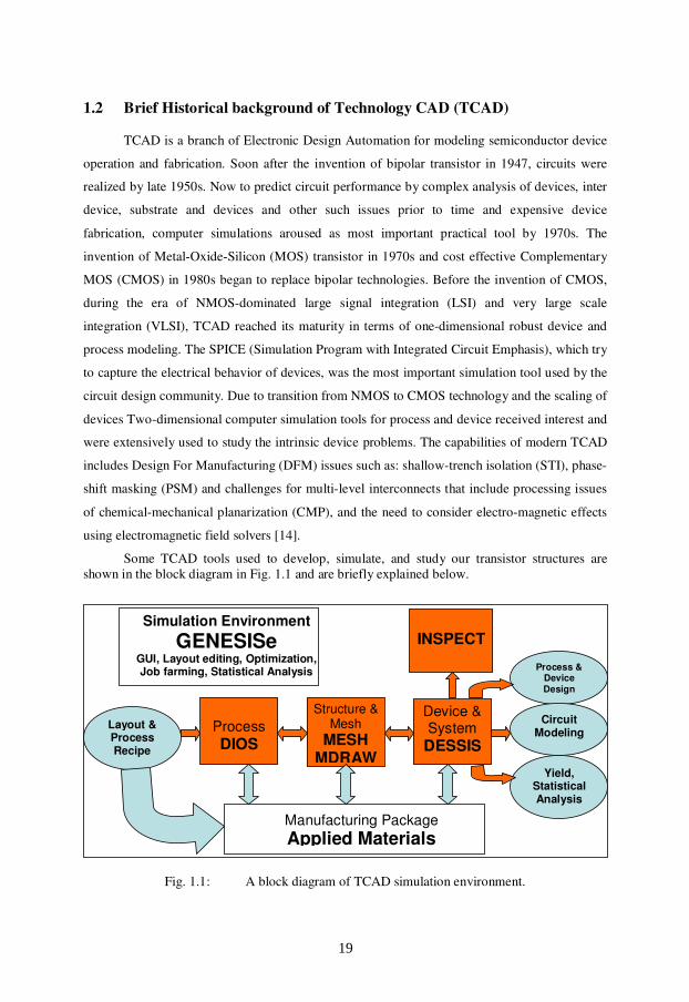
Some TCAD tools used to develop, simulate, and study our transistor structures are shown in the block diagram in Fig. 1.1 and are briefly explained below.
Fig. 1.1: A block diagram of TCAD simulation environment.
Process
DIOS
Structure & Mesh
MESH MDRAW
Device & System
DESSIS
Layout & Process Recipe
Process & Device Design Analysis
Circuit Modeling
Yield, Statistical Analysis
Simulation Environment
GENESISe GUI, Layout editing, Optimization, Job farming, Statistical Analysis
Manufacturing Package
Applied Materials
INSPECT
19

1.2.1 GENESISe
GENESISe is a software package that provides a convenient framework to design,
organize, and automatically run complete TCAD simulation projects. It provides users with a
graphical user interface (GUI) to drive a variety of ISE simulation and visualization tools and
other third-party tools, and to automate the execution of fully parameterized projects. GENESISe
also supports design of experiments (DoE), extraction and analysis of results, optimization, and
uncertainty analysis. It has an integrated job scheduler to speed up simulations and takes full
advantage of distributed, heterogeneous, and corporate computing resources, further details can
be found in ISE-TCAD manual for GENESISe.
1.2.2 MDRAW
It utilizes the graphical user interface (GUI) components, which automatically reflects
the selected environment and offers flexible 2D device boundary editing, doping and refinement
specifications. It defines device structure, doping profile and its refinement, scripting engine that
follows the Tcl (Turbo C++ language) syntax, meshing and griding of selected areas. Each of
these is used to create boundary, doping and refinement information, and meshes adequate for
device simulation.
The meshing part of Mdraw is a GUI-driven front end to Mesh. These meshing tools can
also be called from the command line. The Mdraw components are used to generate and modify
TCAD models to meet specific simulation requirements.
The boundary editor is used to create, modify, and visualize a device structure. It
provides algorithms to preserve the topology correctness (conformity) of the device structure and
to simplify complex structures automatically. The doping editor creates, modify, and visualize
the doping of a device. It also enables the user to specify extra refinement information that
affects the meshing engines by specifying the local mesh size (minimal and maximal allowable
sizes of the elements). MDRAW implements a complete set of analytical models to describe a
wide range of different situations. Analytical profiles are implemented to provide a flexible tool
to simulate process simulation results with ease and within a reasonable time. Further details can
be found in Ref. 15.
1.2.3 DESSIS
DESSIS is a multidimensional, electro thermal, mixed-mode device and circuit simulator
for one-, two-, and three-dimensional semiconductor devices. It incorporates advanced physical
models and robust numeric methods for the simulation of semiconductor devices ranging from
20

diode to very deep submicron Si MOSFETs to large bipolar power structures. In addition, SiC
and III–V compound homo-structure and hetero-structure devices (like SiC MESFET and GaN
HEMT etc.) are fully supported.
DESSIS simulates numerically the electrical behavior of a single semiconductor device
in isolation or several physical devices combined in a circuit. Terminal currents [A], voltages
[V], and charges [C] are computed based on a set of physical device equations that describes the
carrier distribution and conduction mechanisms.
A real semiconductor device, such as a transistor, is represented in the simulator as a
‘virtual’ device whose physical properties are discretized on to a ‘grid’ (or ‘mesh’) of nodes.
Therefore, a virtual device is an approximation of a real device. Continuous properties such as
doping profiles are represented on a sparse mesh and, therefore, are only defined at a finite
number of discrete points in space.
The doping at any point between nodes (or any physical quantity calculated by DESSIS)
can be obtained by interpolation. Each virtual device structure is described in the ISE TCAD tool
suite by two files:
1: The grid (or geometry) file contains a description of the various regions of the device,
that is, boundaries, material types, and the locations of any electrical contacts. This file
also contains the grid (the locations of all the discrete nodes and their connectivity).
2: The data (or doping) file contains the properties of the device, such as the doping
profiles, in the form of data associated with the discrete nodes. By default, a device
simulated in 2D is assumed to have a ‘width’ in the third dimension to be 1 µm. For
further details consult [16].
1.2.4 INSPECT
Inspect is a tool that is used to display and analyze curves. It features a convenient
graphical user interface, a script language, and an interactive language for computations with
curves.
An Inspect curve is a sequence of points defined by an array of x-coordinates and y-
coordinates. An array of coordinates that can be mapped to one of the axes is referred to as a
dataset. With Inspect, datasets can be combined and mapped to the x-axis and y-axis to create
and display a curve.
21

1.2.5 Tec plot
It is dedicated plotting software with extensive 2D and 3D capabilities for post
processing scientific visualizing of data from simulations and experiments. Common tasks
associated with post-processing analysis of flow solver data are, calculating grid quantities,
normalizing data, and verifying solution convergence, estimating the order of accuracy of
solutions and interactively exploring data through cut planes. For further details consult [17 ].
1.3 Fast Fourier Transform (FFT) in MATLAB
MATLAB's FFT function is an effective tool for computing the discrete Fourier
transform of a signal. The FFT is a faster version of the Discrete Fourier Transform (DFT). The
FFT utilizes some clever algorithms to do the same thing as the DTF, but in much less time.
The DFT is extremely important in the area of frequency (spectrum) analysis because it takes a
discrete signal in the time domain and transforms that signal into its discrete frequency domain
representation. Without a discrete-time to discrete-frequency transform we would not be able to
compute the Fourier transform with a microprocessor or DSP based system. It is the speed and
discrete nature of the FFT that allows us to analyze a signal's spectrum with MATLAB.
We used MATLAB to transform our time domain simulation data to frequency domain
using a file already programmed by our group according to our requirements.
1.4 SiC MESFET
The hole mobility of SiC is low, so majority carrier devices, such as MESFETs are
preferred, which do not rely on holes for their operation. The 4H-SiC has been the material of
choice for high frequency SiC MESFETs because of the higher electron mobility in 4H-SiC
(approximately twice that of 6H-SiC). The first SiC MESFETs were fabricated on conducting
substrates, which limits the frequency performance by creating large parasitic capacitances in the
device. The solution is to process devices on highly resistive or semi-insulating (SI) substrates.
In 1996 S. Siriam et al. published the development of 4H-SiC MESFETs on SI substrates [18].
The devices had a gate length of 0.5 um and exhibited fmax of 42 GHz. The output power density
has since climbed to the levels predicted by Trew et al. in [19]; a power density of 5.6 W/mm at
3 GHz has been reported by Cree [20].
The simulations are performed on an enhanced version of a previously fabricated and
tested SiC MESFET transistor [21]. The device has a channel and contact layer thickness and
doping of 200 nm, 3.65 x 1017 cm-3, 100 nm and 1 x 1019 cm-3, respectively. The gate length is
0.5 um. The channel is completely pinched off at -14 V. A maximum drain current is above 550
22

mA/mm at 0 V gate bias. This device showed a breakdown voltage of above 120 V. The DC-IV
characteristics and a schematic of our SiC MESFET structure are shown respectively in Fig. 1.2
& 1.3.
Fig. 1.2: DC IV characteristics of our SiC MESFET.
Fig. 1.3: Schematic of our SiC MESFET structure. In large transistors (for high Power), multiple
gates are combined to increase gate width.
23

1.5 GaN HEMT
The High Electron Mobility Transistor (HEMT) is a commonly used transistor for
microwave and high power amplifiers applications. The idea of world’s first High electron
mobility transistor was presented in the late seventies [11]. Conventional HEMTs on today’s
market has material limitations and scientists have pushed the GaAs material to its theoretical
limit during the last 50 years. New techniques and materials are required for the development of
today’s technology. The GaN is the material of choice for the next generation of HEMT
technology because of its strong physical and electronics properties.
The HEMT is one type of FET family of transistors with excellent high frequency
characteristics. It consists of epitaxial layers grown on top of each other with three contacts
drain, source and gate on the surface. An AlGaN HEMT usually works in depletion mode i.e.
current flows through the device even without an external gate-voltage [22]. The gate voltage
necessary to stop the current flow between the source and drain, and is defined as the pinch-off
voltage. The operation principle of a MESFET is more or less identical to a HEMT with the use
of a Schottky to deplete a channel [23]. When the gate voltage is zero there is a potential well
present at the AlGaN/GaN hetero interface. Inside this well a two-dimensional electron gas will
be formed. The 2DEG is usually a couple of nanometers thick. It is in this thin layer all electrons
are gathered to minimize their energy. This thin channel is also known as a conducting channel
where electrons travel from source to drain. Since the well is very thin, electrons prefer to move
sideways in two dimensions instead of up and down because otherwise they would have to move
out of the well into a less preferable energy state [24]. The AlGaN-GaN hetero junction requires
some special attention due to its polarization fields. The potential profile and amount of charges
induced at the interface in an AlGaN/GaN interface are strongly dependent of the polarization
fields that GaN and AlGaN materials pose [25]. The AlGaN HEMT does not require an n+
doped top layer (like in AlGaAs HEMT for electrons in 2DEG). In fact, the polarization fields
are so strong that it alone can provide high amount of electrons to the junction [22]. The DC-IV
characteristics and schematic of our GaN/AlGaN HEMT structure are shown respectively in Fig.
1.4 & 1.5.
24

0
100
200
300
400
0 10 20 30 40
Drain Voltage VD (V)
Dra
in C
urr
en
t I D
(m
A)
Vg= 0.0 V
Vg= -0.5 V
Vg= -1.0 V
Vg= -1.5 V
Vg= -2.0 V
Vg= -2.5 V
Fig. 1.4: DC IV characteristics of our GaN HEMT.
Figure 1.5: Schematic diagram of GaN/AlGaN HEMT structure.
25

1.6 Silicon Lateral Diffused MOS (Si-LDMOS) FET
The lateral diffused metal-oxide-semiconductor transistor (LDMOS) was developed for
RF applications in 1972 by Sigg. It is widely used for RF power amplification in mobile base
stations at 0.9, 1.8 and 2.6 GHz, due to its high output power together with low cost and large
volume (large diameter Silicon substrate). Due to its high breakdown voltage and high operating
drain voltage, a power density of more than 2W/mm is obtained with a linear gain of 23 dB and
maximum efficiency of 40% at 1 GHz [26].
The LDMOS transistor is a modified device of the MOSFET to enhance the high power
capability. The main modifications are:
1. Low doped and long n-type drift region, which enhances the depletion region and
increases the breakdown voltage. However the on-resistance is high which increases the
losses and degrade the RF performance. Thus, there is always a trade-off between RF
output power and on-resistance.
2. Short channel length created by laterally diffused P-type implantation, which increases
the operating frequency. On the other hand, this feature increases the linearity since the
electrons always transport in the saturation velocity.
3. The sinker principle is used to connect the source to the substrate backside, which
reduces the source inductance, hence, the gain increases. Also the sinker makes the
device integration much easier.
The structure consists of a p-type Si substrate, a low-doped p-type epitaxial layer. Drain
and source regions are highly doped n-type (n+ drain and source). On the drain side a low doped
n- region (Resurf) was added for obtaining higher breakdown voltage. The single source contact
made on the backside of bulk substrate, eliminates the extra surface bond wires. The backside
source contact is established by creating a highly doped, p-type (deep p-well) region by ion
implantation. Therefore device integration is much easier since there are only two contacts left
on the surface namely, drain and gate. The RF performance using such connection is better,
because the source inductance is reduced. The high-frequency properties of Si-LDMOS
transistor is usually determined by the length of the channel region. The shorter channel length
improves the linearity since the transistor always works in velocity saturation [27].
The structure and doping profile of the Infineon LDMOS transistor with source contact at
the bottom of the wafer is shown in Fig. 1.6. We optimized this structure for enhanced DC and
RF performance.
The simulations and measurements were performed on a LDMOS transistor aimed for 28
V power amplifier operations. The structure in Mdraw (2D design Editor of Sentaurus TCAD
26

Software) is obtained from Infineon Technologies. The structure consists of a low-doped p-type
epitaxial layer on a highly doped p+ silicon substrate. Source and drain regions were created
with high doped n-type concentrations. At the drain side, a low-doped n-type RESURF was
introduced. The double-doped offset structure in the RESURF consists of two n-type impurities;
phosphorus (P) and Arsenic (As). An implanted p-type body region was created below the
source and gate regions to define channel length. The lateral diffusion of the dopants and the
dimension of the p_ body region play an important role in controlling the threshold voltage and
drain current saturation. The channel length was adjusted ~0.45 um. The length of source and
RESURF regions were designed 3.4 and 3.25 um, respectively. But due to the diffusion effect of
high doping concentration of drain region, the length of LDD/RESURF region is reduced from
3.25 to 2.8 um. A highly doped p-type (p++) deep region (sinker) was used to connect the source
internally with the substrate. The total length and width of the transistor structure is 12.7 um in X
direction (along the surface) and 19 um in Y-direction (top to bottom) respectively. Aluminum
field plate at the top of the gate and source is used to relax the surface electric field under the
edge of the gate electrode, and to prevent the hot electron degradation. The DC-IV
characteristics of an enhanced version are given in Fig. 1.7. The gate voltages are 3.5–8 V gate
bias with 0.5 V step.
Figure 1.6: Structure and doping profile of the Infineon LDMOS transistor.
27

Fig. 1.7: Comparison of DC-IV characteristics of LDMOS structures with (solid lines) and
without excess interface state charges (dotted lines) at the RESURF region.
1.7 Phased Array System
A phased array system consists of a group of antennas, Tx/Rx modules, beam formers,
signal generators and processors etc. The name phased array originated from the group of
antennas in which the relative phases of the respective signals feeding the antennas are varied in
such a way that the effective radiation pattern of the array is reinforced in a desired direction and
suppressed in undesired directions. Fig. 1.8 shows a block diagram of wideband multifunction
system active phased array system using a single RF front-end to handle functions associated to
radar, EW and communication.
The focus of our class AB PA research work was mainly to study and explore the
potential of wideband gape SiC and GaN transistor amplifiers for use in Tx module of such
systems.
28

Fig. 1.8: A block diagram of wideband multifunction active phased array system.
Beam former including
Control logic, Splitters,
Combiners etc.
Tx/Rx module
Signal Generators, Processors
etc.
Tx/Rx module
Tx/Rx module
Tx/Rx module
Tx/Rx module
A
n
t
e
n
n
a
A
r
r
a
y
29

30

CHAPTER 2
POWER AMPLIFIERS
2 Power Amplifier
Several different types of power amplifiers exist today which differ from each other in
terms of linearity, output power and efficiency for relevant applications. In this chapter, we
present an overview on power amplifiers (PAs); different classes of PA, design considerations
and response of Si-LDMOS, SiC and GaN transistors in power amplifiers.
A typical PA design comprises of several blocks, like biasing network (BN), input
matching network (IMN), output matching network (OMN) for the input and output ports to be
matched with 50 Ohm which is requirement of the system in most cases. There are other
networks (ON) such as feedback network for stability and band width which are implemented as
per requirement. The block diagram is described in Fig. 2.1.
Fig. 2.1: Block diagram of an amplifier.
2.1 Power Amplifier Classes
There are different classes of power amplifiers but a power transistor performance can be
conveniently evaluated using a class-A or class-AB. The class of operation of a power amplifier
depends upon the choice of gate and drain DC voltages called quiescent point (Q-point). The
choice of q-point greatly influences linearity, power and efficiency of the amplifier. The primary
Transistor 50
Ohm 50
Ohm
IMN OMN
BN
ON
31

objective for PA is to provide the required amount of power to antenna. The typical classes of
power amplifiers on the basis of gate biasing are shown in Fig. 2.2. The most common classes
are briefly described below.
Fig. 2.2: Typical classes of power amplifiers on the basis of gate biasing.
2.1.1 Class A
Class-A are the linear amplifiers with the q-point biased close to half of the maximum
drain current. They have low DC power efficiency (theoretically up to 50 %). Figure 2.2 shows
biased q-point for class-A operation. The strongly non-linear effect (overdrive) occurs only when
the drain current exceeds its saturation point (pinch-off) and/or gets into sub threshold region
(cut-off).
2.1.2 Class B
In class-B amplifier, the operation point has to be selected at the threshold voltage to
achieve high power efficiency (theoretically equal to 78 %). In a given case the linear
Class A
Class AB B …E, D, C
Vth (Threshold) VGS
Imax
Imax 2
ID
32

characteristics drastically decrease due to the fact that the conduction angle is half as that for
class-A. There will be current through the device only during half of the input waveform (the
positive part for the N-channel transistor). Hence, the input power capability of such a mode is
almost twice as high.
2.1.3 Class AB
The class-AB amplifier shows a flexible solution for a trade-off between linearity and
efficiency of the previous classes. In this mode the q-point has to be chosen in between A and B
points with its exact place being a matter of application requirements. Therefore, the conduction
angle is typically chosen closer to the threshold voltage as shown in Fig. 2.2. Thus, the transistor
response of class-AB is wider than for class-B due to the operation point. Also, the power
efficiency is higher than for class-A. Many telecommunication applications utilize this mode.
2.1.4 Class C
In the application where linearity is not an issue, and efficiency is critical, non-linear
amplifier classes (C, D, E, F) are used. Class C is an amplifier with a conduction angle of less
than 180 degrees. In Class C, the amplifying device is deliberately operated none linearly as a
switch, in order to reduce resistance losses. In effect, the tank circuit makes the RF output sine
wave. The theoretical efficiency of a typical Class C amplifier approaches 100 %.
2.1.5 Class D
A class-D amplifier, which may also be known as a switching amplifier or a digital
amplifier, utilizes output transistors which are either completely turned on or completely turned
off (switch mode operation). This means that when the transistors are conducting (switched on)
there is virtually no voltage across the transistor and when there is a significant voltage across
the transistor (switched off) there is no current flowing through the transistor. When we have
simultaneous voltage across and current flow through the device, there will be power dissipation
in the form of heat. This heat is wasted power. Class D PA use two or more transistors as
switches to generate square drain-current or voltage waveform.
2.1.6 Class E
Like class-D it also has switch mode operation with some design modification. Class E
PA use single transistor operated as switch. In the ideal situation, the efficiency of a class-E
amplifier is 100%. However, in practice, the switch has a finite on-resistance, and the transition
33

times from the off-state to the on-state and vice-versa are not negligible. Both of these factors
result in power dissipation in the switch and reduce the efficiency.
2.1.7 Class F
The class-F amplifier is one of the highest efficiency amplifiers. It uses harmonic
resonators to achieve high efficiency, which resulted from a low dc voltage current product. In
other words, the drain voltage and current are shaped to minimize their overlap region. The
inductor L and capacitor C are used to implement a third harmonic resonator that makes it
possible to have a third harmonic component in the collector voltage. The output resonator is
used to filter out the harmonic, keeping only the fundamental frequency at the output. The
magnitude and the phase of the third harmonic control the flatness of the collector voltage and
the power of amplifier.
2.1.8 Other High Efficiency PA Classes
There are other high-efficiency amplifiers such as G, H, and S. These classes use
different techniques to reduce the average collector or drain power, which, in sequence, increase
the efficiency. Classes S use a switching technique, while classes G and H use resonators and
multiple power-supply voltage to reduce the current-voltage product.
2.2 Broadband Amplifier
Although there are no set rules to consider an amplifier a broadband or narrow band, an
amplifier is considered to be narrow band when its bandwidth is less than 20 % of the center
frequency. Broadband amplifiers, on the other hand, can cover extremely wide bandwidths.
Amplifiers used in military defense systems and test equipments often require multi decade
frequency range coverage. A single –section networks in amplifiers can generally cover 10 % to
15 % fractional bandwidth easily. Increasing the order of the networks or switching to chip
technology generally helps in the wider bandwidth.
In most of our broadband amplifiers a parallel combination of resistor R1 and capacitor
C3 in series to the input matching network is added in combination with feed back to enhance
stability, increase in bandwidth and to reduce distortion, as shown in Fig. 3.7. In broadband
amplifiers, the active devices have more than the desired gain at lower frequencies. Since we
must give up gain at the lower frequency, the unwanted gain could be dissipated instead of being
reflected (because intentional miss matching for gain flatness increases port reflection
coefficient). The resistor R1 is used for gain equalization (i.e., flat desired gain (GDES) response)
34

by introducing high attenuation at low frequencies (f1) and low attenuation at high frequencies
(f2), while maintaining a good input and output match over the desired broad bandwidth, as
shown in Fig. 2.3.
The value of total feed back resistor controls the gain and bandwidth of the amplifier. If
there is no stability problem, we could increase the gain by reducing the amount of feedback by
increasing the Rfb that also increases the impedances.
Fig. 2.3: The gain equalization (i.e., flat gain response) by introducing high attenuation at low
frequencies and low attenuation at high frequencies.
2.3 Power Amplifier Design Considerations
Designers select the class type to be used based on the application requirements. Class-A,
AB, and B amplifiers have been used for linear applications such as amplitude modulation
(AM), single-sideband modulation (SSB), and quadrate amplitude modulation (QAM). Also it
can be used in linear and wide-band applications such as the multi–carrier power amplifier.
Classes C, D, E, F, G, and H have satisfied the need for narrowband tuned amplifiers of higher
efficiency. Such applications include amplification of FM signals.
Decrease Gain
f1 f2
Gain
G DES
Increase Gain |S21|
2
Freq.
35

The descriptions of power amplifiers in the previous section have dealt with ideal
devices. In reality, transistor amplifiers suffer from a number of limitations that influence
amplifier operation and ultimately reduce their efficiency and output power. In practical FET,
there are four fundamental effects that force the operation of FET to deviate from the ideal case:
the drain source resistance, the maximum channel current If, the open channel avalanche
breakdown voltage, and the drain-source break down voltage.
The following are the major properties of amplifiers, which a designer has to consider in
designing.
2.3.1 Output Power
It is the actual amount of power (in watts) of RF energy that a power amplifier produces
at its output. Power transistors are the most expensive components in power amplifiers. In cost
driven designs, designers are constrained to use cost effective transistors.
2.3.2 Power Gain
The gain of an amplifier is the ratio of an output power to its input power at the
fundamental frequency.
G = POUT/PIN (2.1)
There are three important power gains, an average power gain, transducer power gain and
available power gain.
2.3.3 Efficiency
Efficiency in power amplifiers is expressed as the part of the dc power that is converted
to RF power, and there are three definitions of efficiency that are commonly used.
2.3.3.1 Drain Efficiency (DE)
It is the ratio of the RF-output power to the dc input power.
η= POUT/Pdc (2.2)
2.3.3.2 Power-Added Efficiency (PAE)
PAE includes the effect of the drive power used frequently at microwave frequencies.
PAE is generally used for analyzing PA performance when the gain is high It is a crucial parameter
for RF power amplifiers. It is important when the available input power is limited, like mobile
36

etc. It is also important for high power equipment, when the cooling system cost is significant
compared to actual equipment.
PAE= (POUT - PIN)/Pdc = η (1- 1/G) (2.3)
2.3.3.3 Overall Efficiency (OAE)
It is the form of efficiency usable for all kinds of performance evaluations.
Poverall= POUT/ (Pdc + PIN) (2.4)
2.3.4 Stability
It is a major concern in RF and microwave amplifiers. The degree of amplifier stability
can be quantified by a stability factor. The transistor is stable and will not oscillate when
embedded between 50-Ω source and load. However, this is not considered unconditional
stability, because with different source and load impedances the amplifier might break into
oscillation. A properly designed (stabilized) amplifier will not oscillate no matter what passive
source and load impedances are presented to it, including short or open circuits of any phase.
We apply µ-factor method in our simulations to verify the unconditional stability of the
designs. And if µ > 1 and µ’ > 1, then the 2-port network is unconditionally stable. No conditions
of ∆ (using K factor for stability K > 1 & ∆ < 1) is required and by studying µ and µ’ one could
get a better feel for exactly where the instability phenomenon are conceivable. Here µ describes
the stability at the load (drain) and µ’ at the source (gate).
2.3.5 Linearity
In reality, amplifiers (not ideal) are only linear within certain practical limits. When the
signal drive to the amplifier is increased, the output also increases until a point is reached where
some part of the amplifier becomes saturated and cannot produce more power; this is called
clipping, and results in non-linearity. Class A is the most linear and lowest efficeny PA. The
linearity decreases and effeciency increases when we go to class AB, B, C and switching power
amplifiers.
The non-linearity of a power amplifier can be attributed mainly to gain compression and
harmonic distortions resulting in imperfect reproduction of the amplified signal. It is
characterized by various techniques depending upon specific modulation and application. To
discover it, the circuit response is approximated by the first three terms of Taylor series as:
37

Y (t) ≈ a1X(t) + a2 X 2(t) + a3X
3(t) (2.5)
If a sinusoid is applied to a nonlinear system, the output generally exhibits frequency
components that are integer multiples of the input frequency. In (2.5), if X (t) = Acos ωt, then
Y (t) = a1Acos ωt + a2A2 cos2 ωt + a3A
3 cos3 ωt (2.6)
= a1Acos ωt + (1/2) a2A2 (1 + cos 2ωt) +
(1/4) a3A3 (3 cos ωt + cos 3ωt) (2.7)
= (1/2) a2A2 + (a1A + 3a3A
3 (1/4)) cos ωt +
a2A2 (1/2) cos 2ωt + a3A
3 (1/4) cos 3ωt (2.8)
In (2.8), the term with the input frequency is called the "fundamental" and the higher-
order terms the "harmonics."
Some of the widely used figures for quantifying linearity are explained below;
2.3.5.1 1 dB gain compression (P1dB)
All amplifiers have some maximum output-power capacity, referred to as saturated
power Psat. Driving an amplifier with a greater input signal will not produce an output above this
level. As an amplifier is driven closer to SAT, its deviation from a straight-line response will
increase. The output level will increase by a smaller amount for a fixed increase in input signal
and then reaching saturation. Non-linear response appears in a power amplifier when the output
is driven to a point closer to saturation. At low drive levels, the output power is proportional to
the input power. As the input level approaches saturation point, the amplifier gain falls off, or
compresses. The output level at which the gain compresses by 1 dB from its linear value is
called P1dB. Figure 2.4 shows the relationship between the input and output power and P1dB of a
typical power amplifier.
38

Fig. 2.4: POUT vs PIN, 1 dB compression point [28]
2.3.5.2 Input and Output Intercept point (IIP3 & OIP3)
It is defined as the point where the linear extension of the particular distortion component
intersects the linear extension of the input vs. output line. The third order intercept point (IP3) in
a plot of input power versus the output power is shown in Figure 2.3. This parameter plays a
major role in the analysis of device performance, because higher the IP3, lower is the distortion
at higher power levels.
IIP3= OIP3 – Gain (2.9)
And
OIP3= Pout + PIMD3/2 (2.10)
2.3.5.3 Intermodulation Distortion
It is a phenomenon of generation of undesirable mixing products, which distort the
fundamental tones and gives rise to intermodulation products. The third order intermodulation
IP3
OIP3
IIP3
39

products have the maximum effect on the signal, as they are the closest to the fundamental tone.
The unwanted spectral components, such as the harmonics, can be filtered out. But the filtering
does not work with the third order intermodulation products, as they are too close to the
fundamental tone. Figure 2.5 shows the frequency domain representation of the intermodulation
distortion caused due to a two-tone signal.
If f1 and f2 are the fundamental frequencies then the intermodulation products are seen at
frequencies given by
fIMD = ± m f1 ± n f2 (2.11)
The ratio of power in the intermodulation product to the power in one of the fundamental
tones is used to quantify intermodulation. Of all the possible intermodulation products the third
order intermodulation products are at frequencies 2 f1 - f2 and 2 f2 - f1 and are typically the most
critical.
IMD (dBc) = P1dB – PIMD3 (2.12)
Fig. 2.5: Schematic representation of two-tone intermodulation distortion
2.4 Performance of SiC transistors in Power Amplifiers
SiC exists in a large number of cubic (C), hexagonal (H) and rhombohedral (R) polytype
structures. It varies in the literature between 150 and 250 different poly types. For microwave
and high temperature applications the 4H is the most suitable and popular polytype. Its carrier
f1 f2 f1 f2 2f2-f1 3f2-2f1 3f1-2f2 2f1-f2
IMD3 Gain
PA
40

mobility is higher than in the 6H-SiC polytype (which is also commercially available). For
microwave, high temperature and power applications 4H-SiC is competing with Si and GaAs up
to X- band applications.
The efficiency improvement of power amplifiers decreases power consumption and heat
sink requirements, and increases output power because power amplifiers account for the majority
of power consumption in wireless communications. Therefore, the switching-mode power
amplifiers have recently received attention to improve efficiency. A high efficiency, class-E RF
power amplifier in the VHF range is implemented. A maximum drain dc to RF efficiency of
87% was predicted and 86.8 % achieved with 20.5 W output power at 30 V drain voltage [29].
The SiC MESFETs used appear to offer significant advantages over gallium arsenide (GaAs)
transistors (particularly for space applications) which are inherently low voltage device and more
difficult to operate in class-E due to the high drain peak voltage occurring in this class of
operation.
Another class-E power amplifier using SiC MESFET is reported with power added
efficiency (PAE) of 72.3% and a gain of 10.3 dB at an output power of 40.3 dBm, through
significant reduction of harmonic power levels [30]. A new type of pulse input class C power
amplifier is reported with a maximum PAE of 80% at 500 MHz, a gain of 36.9 dB and power
density of 1.07 W/mm [31].
A power amplifier (PA) for WiMAX Military Applications in Nato Band I (225 to
400MHz) has been simulated, assembled and tested. Under 802.16 OFDM 64QAM3/4
modulations, the average output power is 25W throughout the bandwidth [32]. A class-E power
amplifier using a SiC MESFET is designed and tested at 2.14 GHz. The peak power-added
efficiency of 72.3% with a power gain of 10.27 dB is achieved at an output power of 40.27
dBm [33].
Most publications on SiC microwave components concerns L to C-band operation, since
these are important radar frequency bands. However, the frequency performance up to the X
band has been predicted to be good [34] and SiC MESFETs with power densities of 4.5 W/mm
at 10 GHz have been demonstrated [35]. The power amplifier is a narrow-band 3–3.5-GHz
design based on a 6-mm SiC MESFET. The amplifier was measured on-wafer and showed a
typical power gain of 7 dB, an output power of 2.5 W in continuous wave (CW) operation, and
8W in pulsed mode at 3 GHz. [36]
A single-stage 26 W negative feedback power amplifier is implemented, covering the
frequency range 200-500 MHz using a 6 mm SiC Lateral Epitaxy MESFET. The results at 60 V
drain bias at 500 MHz are, 24.9 dB power gain, 44.15 dBm output power (26 W) and 66 % PAE
41

[37]. Previous reports on SiC MESFET transistor amplifiers designed for frequencies below 500
MHz showed an output power of 37.5 W and a power density of 1.78 W/mm, the gain was 8 dB,
and the efficiency in class A-AB was 55 % at 500 MHz. The IMD3 level at 10 dB back-off from
P 1dB was -35 dBc for a 1 MHz frequency offset between tones [38].
A Class C mode power amplifier is implemented with a 75 V power supply voltage. The
total output power was measured to be 2100 W with a power gain of 6.3 dB, collector efficiency
of 45% and power added efficiency of 35%. This is the first time; SiC BJTs have been used to
produce an output power of 2 kW at 425 MHz. Although the gain and PAE are not very high, the
individual cells are capable of producing 50 W with a gain of 9.3 dB and 51% collector
efficiency. [39]. Two SiC MESFET package and prototype power amplifier were demonstrated
with P1dB output power of 26 and 35W, respectively. High power and high power gain were
maintained through L-band operation across 500 MHz bandwidth (950 MHz to 1500 MHz with
l0 dB gain) for the SiC PA module, which will be a critical challenge to other semiconductor
devices [40].
These results show that although SiC based PAs presently can’t compete with GaN and
other conventional devices like GaAs in terms of frequency but in terms of power and efficiency,
they could be the strong competitors and future devices for, RADAR, Electronic Warfare (EW),
Wireless Communications and base stations applications.
2.5 Performance of GaN transistors in Power Amplifiers
In the last decade, AlGaN/GaN HEMT technology has established itself as a strong
contender for the applications of phase array radars, wireless communication market and other
traditional military applications because of its large electron velocity (>107 cm/s), wide bandgap
(3.4 eV), high breakdown voltage (> 50 V for fT =50 GHz) and sheet carrier concentration
(>1013 cm-2). Due to the superior electronic properties of the GaN semiconductor and the
possibility to use SiC substrate demonstrating high thermal conductivity (3.5 W/cm.K), power
densities as high as 30 W/mm @ 4 GHz [41] as well as output power of 500 W @ 1.5 GHz [42]
have already been achieved. An output power of 75 W of a packaged single-ended GaN-FET has
been reported under pulsed conditions for L/S band applications [43].
The GaN technology is widely used for power amplifier applications. In mobile base
station, a number of manufacturers and researchers have reported high efficiencies, output
powers and power densities [44]–[65]. A class-E amplifier at 13.56 MHz with a high-voltage
GaN HEMT as the main switching device is demonstrated to show the possibility of using GaN
HEMTs in high frequency switching power applications such as power-supply. The 380 V/1.9
42

GaN power HEMT was designed and fabricated for high voltage power electronics applications.
The circuit demonstrated has achieved the output power of 13.4 W and the power efficiency of
91 % under a drain–peak voltage as high as 330 V. This result shows that high-voltage GaN
devices are suitable for high-frequency switching applications under high dc input voltages of
over 100 V. [44]. The Eudyna GaN hybrid power amplifier is capable of efficiently delivering
200 W at 2.1 GHz for W-CDMA applications [45].
The saturated Doherty power amplifier implemented using two Eudyna EGN010MK
GaN HEMTs with a 10 W peak envelope power for 2.14 GHz forward-link W-CDMA signal.
The amplifier delivers an excellent efficiency of 52.4% with an acceptable linearity of 28.3 dBc
at an average output power of 36 dBm. Moreover, the amplifier can provide the high linearity
performance of 50 dBc using the digital feedback pre-distortion technique [46]. A wideband
envelope tracking Doherty amplifier, implemented using Eudyna 10 W GaN high electron
mobility transistor for world interoperability for microwave access (WiMAX) signals of the
802.16 d and 802.16 e, the Doherty amplifier covers the 90 MHz bandwidth. The envelope
tracking amplifier delivers a significantly improved relative constellation error (RCE)
performance of 35.3 dB, which is an enhancement of about 4.3 dB, maintaining the high PAE of
about 30 % for the 802.16 d signal at an average output power of 35 dBm [47].
An ultra wide-band high efficiency power amplifier (PA) is implemented in GaN
technology as shown in Fig. 3. A HEMT device with 1 mm of gate periphery at 0.8-4 GHz,
showing drain efficiency greater than 40% with an output power higher than 32 dBm in the
overall bandwidth [48]. CREE Inc. has also demonstrated compact, high-power microwave
amplifiers taking advantage of the high-voltage and high power density of GaN HEMTs [54]. A
peak power of 550 W (57.40 dBm) is achieved at 3.45 GHz with 66% DE and 12.5 dB
associated gain. An outstanding power-efficiency combination of 521 W and 72.4% is obtained
at 3.55 GHz. Such power levels, accompanied by the high efficiencies, are believed to be the
highest at around 3.5 GHz for a fully-matched, single-package solid-state power amplifier,
attesting the great potential of the GaN HEMT technology.
The state-of-the-art efficiency over 50% drain efficiency (over 45 % PAE) of GaN
HEMT high power amplifier with over 50 W output power at C-band is proposed and
implemented in [55]. A 16 mm gate periphery will be enough for 60 W output power for this
power density. Considering that GaAs demands 75.6 mm gate-width for 20 W output [56], a
230 mm total gate width would be needed to realize 60 W. Therefore, GaN HEMT devices are
desirable to realize broadband high power amplifier.
43

A 2-stage amplifier up with the 30 W driver stage amplifier, 42 % efficiency (including
30 W driver amplifier) and -50 dBc ACLR at the average power of 49 dBm (80 W) with
saturation power of 56.5 dBm and Gain of 32 dB is obtained for WCDMA applications [57]. A
0.4 mm wide GaN device with 0.15-gm gate and 0.25-gm field plate operated up to 60 V
achieved 13.7 W/mm power densities at 30 GHz, the highest for a FET at millimeter-wave
frequencies [58].
A highly efficient, wide band power amplifier designed in GaN technology and utilizing
a non-uniform distributed topology is reported. Measured results demonstrate very high
efficiency across the multi-octave bandwidth. Average CW output power and PAE across 2-
15 GHz was 5.5 W and 25 %, respectively. Maximum output power reached 6.9 W with 32 %
PAE at 7 GHz. [59]. The results obtained for class-E power amplifier using GaN HEMT are; the
power added efficiency (PAE) of 70 % with a gain of 13.0 dB at an output power of 43.0 dBm,
through significant reduction of harmonic power levels [33].
A class F mode PA using Eudyna's GaN HEMT has been biased at class C and adopted a
new output matching topology that improved the overall transmitter efficiency. For the WiMAX
OFDM signal, the calculated overall drain efficiencies of the optimized EER amplifier, which
are based on the measured bias dependent efficiencies, are about 73 % at an average power of
31 dBm at 2.14 GHz. The proposed highly efficient bias modulation PA for the EER transmitter
provides a superior overall efficiency than that of any conventional switching or saturation mode
PAs [60].
A 2-chip amplifier has 220 W output power at C-band, which is the highest output power
ever reported for GaN HEMT amplifiers at C-band and higher bands [61]. A highly efficient
broadband monolithic class-E power amplifier is implemented utilizing a single
0.25 um x 800 um AlGaN/GaN field-plated HEMT producing 8 W/mm of power at 10.0 GHz.
The HPA utilizes a novel distributed broadband class-E load topology to maintain a
simultaneous high PAE and output Power over (6-12 GHz). The HPA’s peak PAE and output
power performance measured under three pulsed drain voltages at 7.5 GHz are: (67 %, 36.8 dBm
@ 20 V), (64 %, 37.8 dBm @ 25 V) and (58 %, 38.3 dBm @ 30 V) [62].
A C-band high-power amplifier with two GaN-based FET chips exhibits record output
powers under continuous-wave (CW) and pulsed operation conditions. At 5.0 GHz, the
developed GaN-FET amplifier delivers a CW 208 W output power with 11.9 dB linear gain and
34 % power-added efficiency. It also shows a pulsed 232 W output power with 8.3 dB linear
gain [63]. A class D−1 amplifier is implemented with GaN MESFETs and working around
900 MHz, delivering 51.1 W output power with 78 % peak drain-efficiency [64].
44

A highly efficient class-F power amplifier (PA) using a GaN HEMT designed at W-
CDMA band of 2.14 GHz has the drain efficiency and power-added efficiency of 75.4 % and
70.9 % with a gain of 12.2 dB at an output power of 40.2 dBm [65]. The GaN HEMTs have also
proven to be very attractive and viable as a power source for millimeter wave applications [66] –
[70]. Similar to microwave frequencies, microstrip and CPW MMICs have been demonstrated,
a microstrip Ka band GaN MMIC power amplifier capable of delivering 11 W of output power
[66]. Wu et al. announced an amplifier with a 1.5-mm-wide device produced 8.05 W output
power at 30 GHz with 31 % PAE and 4.1 dB associated gain. The output power matches that of
a GaAs-based MMIC with a 14.7 m wide output device but with a 10 times smaller size.
Recently, GaN MMIC performance has been demonstrated at W-band as well [70].
The demonstrated high power amplifiers and MMICs with high power densities,
efficiencies and suitable gain will enable the proliferation of solid state solutions at millimeter
wave frequencies.
2.6 Performance of Si-LDMOS transistors in Power Amplifiers
The LDMOS transistors has gone through a great developments in terms of available
output power, power gain, power added efficiency, linearity, frequency of operation and
breakdown voltages for cellular base stations power amplifiers and other wireless standards at
higher frequencies with special focus on the 2.5-2.7 GHz and 3.4-3.8 GHz frequency bands for
WiMAX [71-75]. These are achieved by introducing new device architectures and LDMOS
technology to advanced CMOS fabs.
The RF performance of Freescale Semiconductor's 900 MHz LDMOS technology
demonstrated a 500 W and 41 % efficiency at -55dBc linearity [71]. An internally matched 3 G
WCDMA LDMOS on LTCC (Low Temperature Cofired Ceramic) substrate is demonstrated
with an output power of 180 W, 20 % efficiency and 12 dB of power gain [76]. A highly
efficient Doherty power amplifier was designed for WCDMA application with a peak output
power of 61 W, a gain of 13.5 dB with an efficiency of 43% at PldB and a 9 dB backed-off
efficiency of 22% [77].
Inverse classes F amplifier at 1GHz show 71.9% power added efficiency, 13.2W output
power and 16dB power gain [78]. In another inverse class F amplifier at 1 GHz a PAE of 73.8 %
is achieved with an out power of 12.4 W [79]. Another CMCD amplifier demonstrated a drain
efficiency of 71% with an output power of 20.3 W and a gain of 15.1 dB at 1 GHz [80]. The
class-E power amplifier performance using an LDMOSFET at band of 2.14 GHz show the drain
45

efficiency of 65.2 % with a power gain of 13.8 dB at a Pout of 39.84 dBm. Also, the 2nd- and
3rd-harmonic power levels are reduced below -48 dBc [81].
To lower the cost of the modern base station, in 2000, Freescale introduced the first high
power multistage LDMOS RFIC for the base station market, a 10 W 25dB gain 900 MHz 2 stage
device [74]. They also have reported a highest power LDMOS radio frequency integrated circuit
(RFIC) in plastic over-molded package. The IC targets 1.8 to 2 GHz GSM, EDGE and Evolved
EDGE base station applications. This two-stage, single-chip design exhibits 27 dB of gain and
delivers 132 Watts of output power (1 dB compression; 27 Volt DC supply) with an associated
PAE of 51%. Under EDGE modulation, at an average output power of 46 Watts, the EVM is less
than 1.6 % and the spectral re-growth is –63 dBc and –78 dBc at 400, and 600 kHz offsets,
respectively [82]. Another 25 W Silicon LDMOS 2 stage RFIC is designed for WiMAX
applications at 3.5GHz (3.4 to 3.6 GHz band). Under a 1 tone CW stimulus, this power amplifier
delivers 29 W with a power added efficiency of 36.7 % and 26 dB linear gain [75].
Infineon Technologies is developing a LDMOS IC (LD8IC) process based on 8th
generation discrete technology with integrated passive components. The fT and fmax of LD8IC
technology are 11 GHz and 18 GHz, respectively. Different broadband RF LDMOS PA ICs have
been developed. They can be used for all typical modulation formats from 800 MHz to 2300
MHz, and power levels from 30 W to 50 W depending on application [83].
46

CHAPTER 3
SIMULATION AND MEASUREMENT RESULTS
The performance of wide bandgap SiC and GaN transistors and Si-LDMOS device
during active device simulation is studied using physical transistor structure in Technology
Computer Aided Design (TCAD). A comparison between the physical simulations and measured
device characteristics has been carried out. We optimized GaN HEMT, Si-LDMOS and our
previously fabricated and tested SiC MESFET transistor for enhanced RF and DC-IV
characteristics. For large signal AC performance we developed different computational load pull
(CLP) simulation techniques.
In the second part of our research work, six single stage (using single transistor) power
amplifiers have been designed, fabricated and characterized in three phases for applications in
communications, Phased Array Radars and EW systems.
3.1 Measured Results for PA at VHF frequencies (30-90 MHz)
We designed and fabricated a single-stage class-AB power amplifier at 30-100 MHz
using SiC MESFET. At a drain bias of 50 V for this amplifier the maximum output power
achieved is 46.2 dBm (~42 W) with a power gain of 21 dB and a maximum PAE of 62 %. The
amplifier performance at a higher drain bias of 60 V at 50 MHz, the maximum output power was
46.7 dBm (~47 W) with a power gain of 21 dB and a maximum PAE of 42.7 %. An average
OIP3 of 54 dBm have been achieved for this amplifier. A schematic and results at five different
frequencies are shown respectively in Fig. 3.1 & 3.2.
A two tone intermodulation distortion measurement was carried out at selected
frequencies. The separation between the two carrier tones was 2 MHz. The minimum IMD3
level at 10 dB back-off from P 1dB was 36 dBc at 50 MHz and maximum IMD3 level at 10 dB
back-off from P1dB was 44 dBc at 100 MHz.
47

Fig. 3.1: A schematic of the fabricated power amplifier at 30-100 MHz
10.0
15.0
20.0
25.0
30.0
35.0
40.0
45.0
50.0
0 20 40 60 80 100
f [MHz]
Pm
ax
[d
Bm
] &
Ga
in [
dB
]
0.0
10.0
20.0
30.0
40.0
50.0
60.0
70.0
80.0P
AE
[%
]
Pmax [dBm]
Gain [dB]
PAE [%]
Fig. 3.2 RF power measurements at Vg = -8.5 V and Vd = 50 V at different frequencies.
3.2 Measured Results for PA at UHF frequencies (200-500 MHz)
A single-stage 26 W negative feedback power amplifier is implemented, covering the
frequency range of 200-500 MHz using a 6 mm gate width SiC Lateral Epitaxy MESFET.
48

Typical results for this amplifier at 50 V drain bias for the whole band are, around 22 dB power
gain, 43 dBm output power, minimum power added efficiency at P1dB is 47 % at 200 MHz and
maximum 60 % at 500 MHz. The IMD3 level at 10 dB back-off from P1dB is below -45 dBc. The
results at 60 V drain bias at 500 MHz are; 24.9 dB power gain, output power of 44.15 dBm (26
W) and 66 % PAE, as shown in Fig. 3.3.
Fig. 3.3: Measured results of gain, P1dB, Pmax and PAE at P1dB versus frequency at 60 V.
3.3 Performance Comparison of Three Different Technology Transistors in
Broadband Power Amplifiers (0.7-1.8 GHz)
For performance comparison and to explore the broadband PA potential of SiC MESFET
and two GaN HEMT technologies (GaN on SiC and cost effective GaN on Silicon substrate), we
designed three single stage PAs at 0.7-1.8 GHz.
3.3.1 Measured Results for SiC MESFET Amplifier PA1
The measured maximum output power for the SiC MESFET amplifier PA1 at Vd = 48 V
was 41.3 dBm (~13.7 W), with a PAE of 32 % and a power gain above 10 dB. At a drain bias of
Vd= 66 V at 700 MHz the Pmax was 42.2 dBm (~16.6 W) with a PAE of 34.4 %, the results are
shown in Fig. 3.4.
0
5
1 0
1 5
2 0
2 5
3 0
2 0 0 3 0 0 4 0 0 5 0 0
f M H z ]
Gain
[d
B],
P1d
B[W
],P
max[W
]
0
1 0
2 0
3 0
4 0
5 0
6 0
7 0
PA
E@
P1d
B[%
]
G a in [ d B ]
P 1 d B [ W ]
P m a x [ W ]
P A E @ P 1 d B [% ]
49

A two tone inter modulation distortion measurement was carried out at 1 GHz. The
separation between the two carrier tones was 4 MHz. The IMD3@ 10 dB back off P1dB was -49
dBc and the output IP3 was 53 dBm. The results are shown in Fig. 3.5.
0 .6 0.8 1.0 1 .2 1.4 1.6 1 .8
0
10
20
30
40
50
60
f [G H z]
Ga
in (
dB
) &
P
ma
x (d
Bm
)
Pmax ( dBm )
PAE (%) Ga in (d B)
0
10
20
30
40
50
60
PA
E (%
)
Fig. 3.4: Measured result of gain, Pmax and PAE versus frequency at 48 V drain bias.
-80
-60
-40
-20
0
20
40
60
0 5 10 15 20 25 30
Pin [dBm]
(Pcarr
, P
IM
D3L
,P IM
D5L
) [d
Bm
] P carr both [dBm] P IMD3 low [dBm] P IMD5 low [dBm]
Fig. 3.5: Two tone test results of SiC MESFET PA at 1 GHz, a tone spacing of 4 MHz.
3.3.2 Measured Results for GaN on SiC Amplifier PA2
This amplifier is based on a packaged 10 W GaN HEMT (M1) from Eudyna. It has
lumped matching networks (with shunt feedback between the gate and drain of the active device)
built on the same Rogers Duroid-5880 substrate. A parallel combination of resistor R1 and
50

capacitor C3 in series to the input matching network is added in combination with feed back to
enhance stability, increase in bandwidth and to reduce distortion.
In broadband amplifiers, the active devices have more than the desired gain at lower
frequencies. Since we must give up gain at the lower frequency, the unwanted gain could be
dissipated instead of being reflected (because intentional miss matching for gain flatness
increases port reflection coefficient). The resistor R1 is used for gain equalization (i.e., flat gain
response) by introducing high attenuation at low frequencies and low attenuation at high
frequencies, while maintaining a good input and output match over the desired broad bandwidth.
The feedback network consists of a capacitor Cfb and total resistor of 80 Ω. The resistor is
divided between two 1206 SMT resistors Rfb1 and Rfb2 to enhance power tolerance. The value
of total feed back resistor Rfb (Rfb1 + Rfb2) controls the gain and bandwidth of the amplifier. If
there is no stability problem, we could increase the gain by reducing the amount of feedback by
increasing the Rfb that also increases the impedances. The capacitor Cfb is used to isolate the
gate from the drain bias supply. The capacitor Cfb and bias inductors L2 and L4 also determine
the amplifier’s bandwidth performance, which has to be resonance free across the desired
bandwidth. It was very difficult to obtain unconditional stability without feedback for this
amplifier.
The measured results for GaN HEMT on SiC amplifier PA2 are; maximum output power
at Vd = 48 V is 40 dBm (~10 W), with a PAE of 34 % and a power gain above 10 dB. A two
tone inter-modulation distortion measurement was carried out at 1 GHz. The separation between
the two carrier tones was same as before 4 MHz. The IMD3@ 10 dB back off P1dB was -32 dBc
and the output IP3 was 50 dBm.
Fig. 3.6: A schematic of the fabricated GaN on SiC power amplifier PA2 at 0.7-1.8 GHz
51

0 .6 0.8 1.0 1 .2 1.4 1.6
0
10
20
30
40
50
60
f[G H z]
Ga
in (
dB
) &
P
m
ax (d
Bm
)
P m ax (d B m ) G a in (d B )
P A E ( % )
0
10
20
30
40
50
60
PA
E (%
)
Fig. 3.7: Power measurement results at Vd = 48 V at three different frequencies for PA2
3.3.3 Measured Results for GaN on Si Amplifier PA3
A hybrid amplifier 0.2-1.8 GHz for high power phased array transmitter application has
been designed and fabricated. This amplifier design is based on a large signal model of packaged
15 W GaN HEMT on Si provided by Nitronex.
The measured results for GaN HEMT on Si amplifier PA3 are; maximum output power
is 42.5 dBm (~18 W) with a minimum PAE of 20 % and above 10 dB gain at all measured
frequencies. A picture of fabricated amplifier and results at five different frequencies are shown
respectively in Fig. 3.8 & 3.9.
Fig. 3.8: A picture of the fabricated GaN on Si amplifier PA3
52
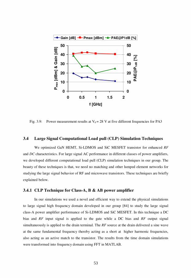
0
10
20
30
40
50
0 0.5 1 1.5 2
f [GHz]
Pm
ax [
dB
m]
& G
ain
[d
B]
0
10
20
30
40
50
PA
E@
P1
dB [
%]
Gain [dB] Pmax [dBm] PAE@P1dB [%]
Fig. 3.9: Power measurement results at Vd = 28 V at five different frequencies for PA3
3.4 Large Signal Computational Load pull (CLP) Simulation Techniques
We optimized GaN HEMT, Si-LDMOS and SiC MESFET transistor for enhanced RF
and DC characteristics. For large signal AC performance in different classes of power amplifiers,
we developed different computational load pull (CLP) simulation techniques in our group. The
beauty of these techniques is that, we need no matching and other lumped element networks for
studying the large signal behavior of RF and microwave transistors. These techniques are briefly
explained below.
3.4.1 CLP Technique for Class-A, B & AB power amplifier
In our simulations we used a novel and efficient way to extend the physical simulations
to large signal high frequency domain developed in our group [84] to study the large signal
class-A power amplifier performance of Si-LDMOS and SiC MESFET. In this technique a DC
bias and RF input signal is applied to the gate while a DC bias and RF output signal
simultaneously is applied to the drain terminal. The RF source at the drain delivered a sine wave
at the same fundamental frequency thereby acting as a short at higher harmonic frequencies,
also acting as an active match to the transistor. The results from the time domain simulations
were transformed into frequency domain using FFT in MATLAB.
53
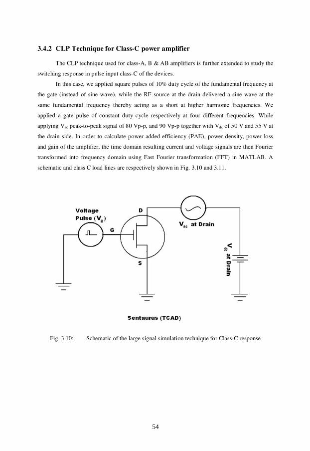
3.4.2 CLP Technique for Class-C power amplifier
The CLP technique used for class-A, B & AB amplifiers is further extended to study the
switching response in pulse input class-C of the devices.
In this case, we applied square pulses of 10% duty cycle of the fundamental frequency at
the gate (instead of sine wave), while the RF source at the drain delivered a sine wave at the
same fundamental frequency thereby acting as a short at higher harmonic frequencies. We
applied a gate pulse of constant duty cycle respectively at four different frequencies. While
applying Vac peak-to-peak signal of 80 Vp-p, and 90 Vp-p together with Vdc of 50 V and 55 V at
the drain side. In order to calculate power added efficiency (PAE), power density, power loss
and gain of the amplifier, the time domain resulting current and voltage signals are then Fourier
transformed into frequency domain using Fast Fourier transformation (FFT) in MATLAB. A
schematic and class C load lines are respectively shown in Fig. 3.10 and 3.11.
Fig. 3.10: Schematic of the large signal simulation technique for Class-C response
54

Fig. 3.11: Pulse input Class-C Load lines at 0.5, 1, 2 & 3 GHz.
3.4.3 CLP Technique for Class-D, E & F power amplifier
The CLP technique used for class-C amplifiers is further extended to study the switching
response in class-F of the devices. This technique can also be used to study class-D & E
characteristics of the transistors.
In our simulations we applied a technique by further modification of our simulation
technique as shown in Fig. 3.10. We applied a square pulse of 10% duty cycle of the
fundamental frequency at the gate and at the same time a square pulse of 10% duty cycle of the
same fundamental frequency is applied at the drain (instead of applying sin wave) thereby acting
as a short at higher harmonic frequencies. We applied gate and drain pulses of constant duty
cycle at 500 MHz, While Vdc of 10 V is also applied at the drain side, so that to provide
sufficient voltage to keep the transistor turn ON. The gate pulse amplitude was 15 V (-15 to 0 V)
with equal time rise (Tr) and time fall (Tf) of 100 pS. The pulse on time (Ton) was 200 pS. The
amplitude of the pulse at the drain was 80 V (10 to 90 V) with equal time rise (Tr) and time fall
(Tf) of 520 pS. The pulse on time (Ton) was 480 pS. In order to calculate power added efficiency
(PAE), power density, switching loss and gain of the amplifier, the time domain resulting current
and voltage signals are then Fourier transformed into frequency domain using Fast Fourier
Transformation (FFT) in MATLAB. The results obtained are given in table 3.1. A schematic
diagram of the technique is shown in Fig. 3.12.
55

Table 3.1: A Summary of class F power amplifier results at 500 MHz.
Freq
[MHz]
Drain
Pulse
[V]
Gate
Pulse
[V]
Drain
Vdc
[V]
PAE
[%]
Pout
[W/mm]
Switching
loss
[W/mm]
Gain
[dB]
500 80 15 10 84 2.75 0.77 26
Fig. 3.12: A Schematic of the large signal TCAD simulation technique for Class-D, E & F
switching characteristics of devices.
56

CHAPTER 4
CONCLUSIONS
In this thesis work we studied SiC MESFET, GaN HEMT and Si-LDMOS devices along
with their applications in different classes of power amplifiers. We studied the performance of
transistors during active device simulation using physical transistor structure in TCAD. A
comparison between the physical simulations and measurements has been carried out. We
optimized GaN HEMT, Si-LDMOS and SiC MESFET transistor for enhanced RF and DC
characteristics. For large signal AC performance we developed different computational load pull
(CLP) simulation techniques. Using these techniques, we studied class A, AB, pulse input class-
C, class-D, E & F switching response of SiC MESFET. We obtained maximum PAE of 78.3 %
with power density of 2.5 W/mm for class C and 84 % for class F power amplifier at 500 MHz.
We also studied Si-LDMOS (transistor structure provided by Infineon Technologies Nordic) for
improved DC and RF performance. The interface charges between the oxide and RESURF
region are used not only to improve DC drain current and RF power, gain & efficiency but also
enhance its operating frequency up to 4 GHz.
We designed, fabricated and characterized six single stage power amplifiers for
applications in communications, Phased Array Radars and EW systems. The first design is 26 W
PA implemented using SiC MESFET covering the frequency band from 200-500 MHz. At 60 V
drain bias at 500 MHz 24.9 dB of power gain, 44.15 dBm output power (26 W) and 66 % PAE is
obtained for this amplifier. The second design is at a frequency band of 30-100 MHz using SiC
MESFET. In this case we achieved a Pmax of 46.7 dBm (~47 W) with a power gain of 21 dB.
Other three broadband class AB power amplifiers are designed and fabricated at 0.7-1.8
GHz for performance comparison of SiC MESFET and two different GaN HEMT technologies
(GaN HEMT on SiC and GaN HEMT on Silicon substrate). The measured maximum output
power for the SiC MESFET amplifier at a drain bias of Vd= 66 V at 700 MHz was 42.2 dBm
(~17 W) with a PAE of 34.4 %. The measured results for GaN HEMT on SiC amplifier are;
maximum output power at Vd = 48 V is 40 dBm (~10 W), with a PAE of 34 % and a power gain
above 10 dB. The measured maximum output power for third amplifier using GaN HEMT on Si
amplifier is 42.5 dBm (~18 W) with a maximum PAE of 39 % and a gain of 19.5 dB.
A high power single stage class E power amplifier is implemented with lumped elements
at 0.89-1.02 GHz using Silicon GaN HEMT as an active device. The maximum drain efficiency
57

(DE) and PAE of 67 and 65 % respectively is obtained with a maximum output power of 42.2
dBm (~ 17 W) and a maximum power gain of 15 dB.
These results show that although SiC based PAs presently can not compete with GaN and
other conventional devices like GaAs in terms of frequency but in terms of power and efficiency,
they could be the strong competitors and future devices for, RADAR, Electronic Warfare (EW),
Wireless Communications and base stations applications. But SiC MESFET and GaN HEMT on
SiC are more costly compare to Silicon based Si-GaN HEMT and Si-LDMOS devices. Due to
low cost and comparable power and efficiency performance these devices are currently used for
Wireless Communications and base stations applications. In the present technology Si-LDMOS
and SiC MESFET has frequency limitations of 4 GHz (theoretically 5 GHz) and 10 GHz
respectively. Thus cost effective Si-GaN HEMTs has a great potential of power, efficiency,
higher frequency and lower cost (large Si substrate). Almost all major properties in a single GaN
technology indicate that Si-GaN would be the possible first choice for different applications.
.
58

REFERENCES
[1] C. E. Weitzel, “Comparison of SiC, GaAs, and Si RF MESFET power densities,” IEEE
Trans. Electron Device Lett., vol. 16, pp. 541-453, Oct. 1995.
[2] Gassmann, J., Watson, P., Kehias, L., and Henry, G. ‘Wideband, high efficiency GaN
power amplifiers utilizing a non-uniform distributed topology’, IEEE MTT-S Int. Microw.
Sym. Dig., 2007, pp. 615–618
[3] Umesh K. Mishra, Fellow IEEE, Likun Shen, Thomas E. Kazior, and Yi-Feng Wu “GaN-
Based RF Power Devices and Amplifiers”, Proceedings of the IEEE, Vol. 96, No. 2,
February 2008.
[4] R. T. Kemerley, H. B. Wallace and M. N. Youder, “Impact of wide bandgap microwave
devices on DoD systems”, Proc. IEEE, vol. 90, no. 6, 2002
[5] J. W. Palmour, “Energy Efficiency: The Commercial Pull for SiC Devices”, Materials
Science Forum Vols. 527-529 (2006) pp 1129-1134
[6] R. G. Davis, “The potential performance of wide bandgap microwave power MESFETs”,
Mat. Sci. and Eng. Vols. B61-62, pp. 419, 1999.
[7] A. W. Morse et al, “Recent applications of silicon carbide to high power microwave,”
Proc. IEEE int. Microwave Symp., 1997, pp. 53-56.
[8] P. G. Neudeck, R. S. Okojie and L. Chen, “High-temperature electronics—A role for wide
bandgap semiconductors?” Proc. IEEE, Vol. 90, no. 6, 2002, pp. 1065- 1076.
[9] H. G. Henry, G. Augustine, G. C. DeSalvo, R. C. Brooks, R. R. Barron, J. D. Oliver, Jr.,
A. W. Morse, B. W. Veasel, P. M. Esker and R. C. Clarke, ” S-band operation of SiC
power MESFET with 20W (4.4 W/mm) output power and 60% PAE,” IEEE Trans.
Electron Devices, Vol. 51, No. 6, 2004, pp. 839-845.
[10] A. Torres, “Advantages of silicon carbide (SiC) RF transistors for driving antenna
impedances,” Antenna measurement techniques association, Oct. 21.26, Denver, 2001.
[11] Takashi Mimura, “The Early History of the High Electron Mobility Transistor (HEMT)”,
IEEE Transactions on microwave theory and techniques, Vol. 50, No. 3, March 2002.
[12] www.freescale.com/files/rf_if/doc/data_sheet/MRF6VP11KH.pdf
[13] L.Vestling, “Design and Modeling of High-Frequency LDMOS Transistor”, Acta
Universitatis Upsaliensis. Comprehensive Summaries of Uppsala Dissertation from the
Faculty of Science and Technology, pp.50, Uppsala. ISBN 91-554- 5210-8, 2002
[14] http://en.wikipedia.org/wiki/Technology_CAD
[15] ISE-TCAD and Synopsis manual for MDRAW
59

[16] ISE-TCAD and Synopsis manual for DESSIS
[17] http://en.wikipedia.org/wiki/Tecplot
[18] S. Sriram, G. Augustine, A. A. Burke, R. C. Glass, H. M. Hobgood, P. A. Orphanos, L. B.
Rowland, T. J. Smith, C. D. Brandt, M. C. Driver and R. H. Hopkins, “4H-SiC
MESFET’s with 42 GHz fmax,” IEEE Electron Device Lett., Vol. 17, no. 7, 1996, pp.
369-371.
[19] R. J. Trew, J. B. Yan and P. M. Mock, “The potential of diamond and SiC electronic
devices for microwave and millimeter-wave power applications,” Proc. IEEE, vol. 79, pp.
598-620, May 1991.
[20] S. T. Allen, W. L. Pribble, R. A. Sadler, T. S. Alcorn, Z. Ring and J. W. Palmour,
“Progress in high power SiC microwave MESFETs,” IEEE MTT-S dig., 1999, pp. 321-
324.
[21] R. Jonsson, Q. Wahab, S. Rudner, C. Svensson,“Computational load pull simulations of
SiC microwave power transistors” Solid State Electronics 2003, Vols. 47 pp. 1921-1926.
[22] David W Disanto, “Aluminum gallium nitride / gallium nitride high electron mobility
transistor fabrication and characterization”, PhD thesis, Simon Fraser University (2005).
[23] Nh Sheng, C. P Lee, “Multiple-Channel GaAs/AlGaAs High Electron Mobility
Transistors”, IEEE Electron device letters, Vol. EDL-6, No. 6. June 1985.
[24] Charles Kittel, “Introduction to solid state physics – eight editions” ISBN 0-471-41526-X,
(2005)
[25] O. Ambacher, B. Foutz, J.Smart, J.R Shealy, “Two dimensional electron gases induced by
spontaneous and piezoelectric polarization in doped and un-doped AlGaN/GaN hetero
structures”, Journal of applied physics Volume 87, number 1 (2000)
[27] J. Olsson et al., 1W/mm RF power density at 3.2 GHz for a dual-layer RESURF LDMOS
transistor, IEEE Electron Device Lett, Vol. 23, pp.206, 2002.
[28] Master thesis by Grigori Doudorov “Evaluation of Si-LDMOS transistor for RF power
amplifier in 2-6 GHz frequency range”, Linkoping University, Linkoping, Sweden.
[29] Marc Franco and Allen Katz, “Class-E Silicon Carbide VHF Power Amplifier”,
Microwave Symposium, 2007, IEEE/MTTS International, pp. 19-22
[30] Yong-Sub Lee and Yoon-Ha Jeong, “Applications of GaN HEMTs and SiC MESFETs in
High Efficiency Class-E Power Amplifier Design for WCDA Applications, Microwave
Symposium, 2007, IEEE/MTTS International, pp. 615-618
[31] Sher Azam, C. Svensson and Q. Wahab “Designing of High Efficiency Power Amplifier
Based on Physical Model of SiC MESFET in TCAD.” Proceedings of International
60

Bhurban Conference on Applied Sciences & Technology Islamabad, Pakistan, 8th- 11th
January, 2007, pp. 40-43.
[32] Luca Risso, Alberto Armoni and Luca Petacchi“A 225-400MHz WiMAX 20W SiC
Power Amplifier” Proceedings of the 37th European Microwave Conference, October
2007, Munich Germany, pp. 1291-1294.
[33] Yong-Sub Lee and Yoon-Ha Jeong, “A HIGH-EFFICIENCY CLASS-E POWER
AMPLIFIER USING SiC MESFET” Microwave and Optical Technology Letters / Vol.
49, No. 6, June 2007
[34] Mattias Sudow et al. “A SiC MESFET-Based MMIC Process,” IEEE Transactions on
Microwave Theory and Techniques, VOL. 54, NO. 12, December 2006, pp. 4072–4079.
[35] R. J. Trew, “Experimental and simulated results of SiC microwave power MESFETs,”
Phys. Stat. Sol. A, vol. 162, no. 1, pp. 409–419, Jul. 1997.
[36] R. Sadler, S. Allen, W. Pribble, T. Alcorn, J. Sumakeris, and J. Palmour, “SiC MESFET
hybrid amplifier with 30-W output power at 10 GHz,” in Proc. IEEE/Cornell Conf. High
Performance Devices, Aug. 2000, pp. 173–177.
[37] Sher Azam, R. Jonsson and Q. Wahab “Single-stage, High Efficiency, 26-Watt power
Amplifier using SiC LE-MESFET” IEEE Asia Pacific Microwave Conf. (APMC), Yoko
Hama (Japan), pp. 441–444, December 2006.
[38] F.Villard, J.-P.Prigent, E.Morvan, C.Dua, C.Brylinski, T.Temcamini and P.Pouvil Trap-
Free Process and Thermal Limitations on Large- Periphery SiC MESFET for RF and
Microwave Power”, IEEE Trans MTT, Vol. 51, pp.1129- 1134 (2003)
[39] Anant Agarwal, Jeremy Haley, Howard Bartlow, Bill McCalpin, Craig Capel, John W.
Palmour “2100 W at 425 MHz with SiC RF Power BJTs ” 63rd Device Research
Conference, 2005, pp. 189–190.
[40] P. Chen, H.R. Chang, X. Li and Ben Luo,“DESIGN AND FABRICATION OF SIC
MESFET TRANSISTOR AND BROADBAND POWER AMPLIFIER FOR RF
APPLICATIONS”, Proceedings of 2004 International Symposium on Power
Semiconductor Devices & ICs, Kitakyushu, pp. 317–318.
[41] Y.-F. Wu, A. Saxler, M. Moore, R. P. Smith, S. Sheppard, P. M. Chavarkar, T. Wisleder,
U. K. Mishra, and P. Parikh, 30-W/mm GaN HEMTs by Field Plate Optimization, IEEE
Electron device Letters, vol. 25, no. 3, March 2004, pp 117-119 .
[42] A. Maekawa, T. Yamamoto, E. Mitani and S. Sano, “A 500W Push Pull AlGaN/GaN
HEMT Amplifier for L-Band High Power Application”, 2006 IEEE MTT-S Int.
Microwave Symp. Digest pages 722-725, June 2006.
61

[43] A. Wakejima, T. Nakayama, K. Ota, Y. Okamoto, Y. Ando, N. Kuroda, M. Tanomura, K.
Matsunaga and H. Miyamoto, “Pulsed 0.75kW output single-ended GaN-FET amplifier
for L/S band applications”, Electronics Letters, Vol. 42, Nov. 2006.
[44] Saito Wataru, Domon Tomokazu, Omura Ichiro, Kuraguchi Masa-hiko, Takada
Yoshiharu, Tsuda Kunio, et al. Demonstration of 13.56-MHz Class-E amplifier using a
high-voltage GaN power-HEMT. IEEE Electron Dev Lett 2006; 27(5):326–8. 235
[45] A. Kawano, N. Adachi, Y. Tateno, S. Mizuno, N. Ui, J. Nikaido, and S. Sano, “High-
efficiency and wide-band single-ended 200 W GaN HEMT power amplifier for 2.1 GHz
W-CDMA base station application, in APMC 2005 Asia-Pacific Conference Proceedings,
Dec. 2005, vol. 3, pp. 4–7.
[46] Jangheon Kim, Junghwan Moon, Young Yun Woo, Sungchul Hong, Ildu Kim, Jungjoon
Kim, and Bumman Kim, “Analysis of a Fully Matched Saturated Doherty Amplifier With
Excellent Efficiency”, IEEE Transactions on Microwave Theory and Techniques, VOL.
56, NO. 2, FEBRUARY 2008
[47] Junghwan Moon, Jangheon Kim, Ildu Kim, Jungjoon Kim, and Bumman Kim, “A
Wideband Envelope Tracking Doherty Amplifier for WiMAX Systems”, IEEE
Microwave and Wireless Components Letters, VOL. 18, NO. 1, January 2008.
[48] P. Colantonio, F. Giannini, R. Giofre` and L. Piazzon, “High-efficiency ultra-wideband
power amplifier in GaN technology”, ELECTRONICS LETTERS 17th January 2008 Vol.
44 No. 2
[49] T. Kikkawa, T. Maniwa, H. Hayashi, M. Kanamura, S. Yokokawa, M. Nishi, N. Adachi,
M. Yokoyama, Y. Tateno, and K. Joshin, BAn over 200-W output power GaN HEMT
push-pull amplifier with high reliability, in Microwave Symposium Digest, 2004 IEEE
MTT-S International, Jun. 2004, vol. 3, pp. 1347–1350.
[50] S. T. Sheppard, R. P. Smith, W. L. Pribble, Z. Ring, T. Smith, S. T. Allen, J. Milligan, and
J. W. Palmour, “High power hybrid and MMIC amplifiers using wide-bandgap
semiconductor devices on semi-insulating SiC substrates, in Device Research
Conference, 2002. 60th DRC. Conference Digest, Jun. 24–26, 2002, pp. 175–178.
[51] K. Yamanaka, K. Iyomasa, H. Ohtsuka, M. Nakayama, Y. Tsuyama, T. Kunii, Y. Kamo,
and T. Takagi, “S and C band over 100W GaN HEMT 1-chip high power amplifiers with
cell division configuration,[ in Gallium Arsenide and Other Semiconductor Application
Symposium, 2005. EGAAS 2005. European, Oct. 3–4, 2005, pp. 241–244.
62

[52] T. Kikkawa, “Recent progress and future prospects of GaN HEMTs for base-station
applications, IEEE Compound Semiconductor Integrated Circuit Symposium, Oct. 2004,
pp. 17–20.
[53] A. Maekawa, M. Nagahara, T. Yamamoto, and S. Sano, “100 W high-efficiency GaN
HEMT amplifier for S-band wireless system”, in Gallium Arsenide and Other
Semiconductor Application Symposium, Oct. 2005, pp. 497–500.
[54] Y.-F. Wu, S. M. Wood, R. P. Smith, S. Sheppard, S. T. Allen, P. Parikh, and J. Milligan,
“An internally-matched GaN HEMT amplifier with 550-watt peak power at 3.5 GHz,
IEEE International Electron Devices Meeting, 2006.
[55] Kazuhiro Jyomasa', Koji Yamanaka', Kazutomi Mori, Hifumi Noto, Hiroshi Ohtsuka,
Masatoshi Nakayama, Satoshi Yoneda, Yoshitaka Kamo, and Yoji Isota, “GaN HEMT
60W Output Power Amplifier with Over 50% Efficiency at C-Band 15% Relative
Bandwidth Using Combined Short and Open Circuited Stubs, in IEEE IMS, 2007,
pp.1255-1258.
[56] H. Otsuka, K. Mori, H. Yukawa, H. Minamide, Y. Kittaka, T. Tsunoda, S. Ogura, Y.
Ikeda, T. Takagi, "Over 65% efficiency 300 MHz bandwidth C-band internally-matched
GaAs FET designed with a large-signal FET model," 2004 IEEE MTT-S int. Microwave
Symp. Dig., pp. 521-524, June 2004.
[57] Norihiko Ui. Hiroaki Sano and Seigo Sano, “A 80W 2-stage GaN HEMT Doherty
Amplifier with -5OdBc ACLR, 42% Efficiency 32dB Gain with DPD for W-CDMA Base
station,[ in IEEE IMS, 2007, pp. 1259-1262
[58] Y.-F. Wu, M. Moore, A. Abrahamsen, M. Jacob-Mitos, P. Parikh, S. Heikman, and A.
Burk, “High-voltage Millimeter-Wave GaN HEMTs with 13.7 W/mm Power Density,
Electron Device Meeting, 2007. IEDM2007. IEEE International, pp. 405-407
[59] J. Gassmann, P. Watson, L. Kehias and G. Henry “Wideband, High-Efficiency GaN
Power Amplifiers Utilizing a Non-Uniform Distributed Topology , Microwave
Symposium, 2007, IEEE/MTTS International, pp. 615-618
[60] Sungchul Hong, Young Yun Woo, Ildu Kim, Jangheon Kim, Junghwan Moon, Han Seok
Kim, Jong Sung Lee and Bumman Kim, “High Efficiency GaN HEMT Power Amplifier
optimized for OFDM EER Transmitter , Microwave Symposium, 2007, IEEE/MTTS
International, pp. 1247-1250
[61] K. Yamanaka, K. Mori, K. Iyomasa, H. Ohtsuka, H. Noto, M. Nakayama, Y. Kamo , and
Y. Isota “C-band GaN HEMT Power Amplifier with 220W Output Power”, Microwave
Symposium, 2007, IEEE/MTTS International, pp. 1251-1254
63

[62] R. Tayrani “A Spectrally pure 5.0 W, High PAE, (6-12 GHz) GaN Monolithic Class E
Power Amplifier for Advanced T/R Modules, IEEE Radio Frequency Integrated Circuits
Symposium 2007, pp. 581-584
[63] Y. Okamoto, T. Nakayama, Y. Ando, A. Wakejima, K. Matsunaga, K. Ota and H.
Miyamoto “230W C-band GaN-FET power amplifier, Electronics Letters August 16,
2007, Vol. 43 No. 17, pp. 1-2
[64] Ulf Gustavsson, Thomas Lejon, Christian Fager , Herbert Zirath “Design of highly
efficient, high output power, L-band class D−1 RF power amplifiers using GaN MESFET
devices. Proceedings of 2nd European IC Conference, October 2007, Munich Germany,
pp. 91-294
[65] Yong-Sub Lee, Mun-Woo Lee, and Yoon-Ha Jeong, “High-Efficiency Class-F GaN
HEMT Amplifier with Simple Parasitic Compensation Circuit”, IEEE Microwave and
Wireless Components Letters, VOL. 18, NO. 1, JANUARY 2008.
[66] M. Kanamura, T. Kikkawa, and K. Joshin, “A 100-W high-gain AlGaN/GaN HEMT
power amplifier on a conductive n-SiC substrate for wireless base station applications,
EEE IEDM Technical Digest, Dec. 2004, pp. 799–802.
[67] D. C. Streit, A. Gutierrez-Aitken, M. Wojtowicz, and R. Lai, “The future of compound
semiconductors for aerospace and defense applications, in Compound Semiconductor
Integrated Circuit Symposium, 2005. CSIC ’05, Oct. 2005, p. 4.
[68] M. Micovic, A. Kurdoghlian, H. P. Moyer, P. Hashimoto, A. Schmitz, I. Milosavjevic, P.
J. Willadesn, W.-S. Wong, J. Duvall, M. Hu, M. J. Delaney, and D. H. Chow, “Ka-band
MMIC power amplifier in GaN HFET technology, IEEE MTT-S International Microwave
Symposium Digest, Jun. 2004, vol. 3, pp. 1653–1656.
[69] A. Darwish, K. Boutros, B. Luo, B. D. Huebschman, E. Viveiros, and H. A. Hung,
“AlGaN/GaN Ka-band 5-W MMIC amplifier, IEEE Trans. Microwave Theory and
Techniques, to be published.
[70] Y.-F. Wu, M. Moore, A. Saxler, T. Wisleder, U. K. Mishra, and P. Parikh, “8-watt GaN
HEMTs at millimeter wave frequencies, IEEE International Electron Devices Meeting,
IEDM Technical Digest, Dec. 5–7, 2005, pp. 583–585.
[71] Burns, C.T.; Chang, A.; Runton, D.W.; “A 900 MHz, 500 W Doherty Power Amplifier
Using Optimized Output Matched Si LDMOS Power Transistors” Microwave
Symposium, 2007. IEEE/MTT-S International, 3-8 June 2007 Page(s):1577 – 1580
64

[72] Qiao, M.; Zhang, B.; Li, Z.J.; Fang, J. “Analysis of back-gate effect on breakdown
behaviour of over 600V SOI LDMOS transistors”, Electronics Letters Volume 43, Issue
22, Oct. 25 2007.
[73] Zhang, H.P.; Sun, L.L.; Jiang, L.F.; Xu, L.Y.; Lin, M. “Process simulation of trench gate
and plate and trench drain SOI nLDMOS with TCAD tools”, Semiconductor Electronics,
2008. ICSE 2008. IEEE International Conference on Volume, Issue, 25-27 Nov. 2008
Page(s):92 - 95
[74] G. Bouisse "High power Silicon MMIC design for wireless base stations." IEEE EuMw
symposium, 2000
[75] Cassan, C.; Gola, P.; “A 3.5 GHz 25 W Silicon LDMOS RFIC power amplifier for
WiMAX applications”, Radio Frequency Integrated Circuits (RFIC) Symposium, 2007
IEEE 3-5 June 2007 Page(s):87 – 90
[76] Estes, J.; Piel, P.; Shapiro, G.; Pavio, A.; Hurst, M.; Call, J.; Funk, G.; “ internally
matched LTCC 3G W-CDMA 180 watt LDMOS power amplifier”, Microwave
Symposium Digest, 2001 IEEE MTT-S International Volume 2, 20-25 May 2001
Page(s):1357 - 1358 vol.2
[77] Beishline, D.W.; Cassan, C.; Elsharawy, E.A.; Aly, A.; “Highly efficient 60 watt W-
CDMA LDMOS power amplifier using the modified doherty configuration”, Microwave
Conference, 2004. 34th European Volume 3, 11-15 Oct. 2004 Page(s):1169 – 1172
[78] Ouyahia, A.; Duperrier, C.; Tolant, C.; Temcamani, F.; Eudeline, Ph.; “A 71.9% power-
added-efficiency inverse Class-FLDMOS”, Microwave Symposium Digest, 2006. IEEE
MTT-S International 11-16 June 2006 Page(s):1542 – 1545
[79] Lepine, F.; Adahl, A.; Zirath, H.; “A high efficient LDMOS power amplifier based on an
inverse class F architecture”, Microwave Conference, 2004. 34th European Volume 3, 11-
15 Oct. 2004 Page(s):1181 – 1184
[80] Hussein Mashad Nemati, Christian Fager, Herbert Zirath, “High Efficiency LDMOS
Current Mode Class-D Power amplifier at 1 GHz”, Proceedings of 36th European
Microwave Conference EuMC 2006.
[81] Yong-Sub Lee; Kye-Ik Jeon; Yoon-Ha Jeong; “A 2.14 GHz class-E LDMOS power
amplifier”, Microwave Conference, 2006. APMC 2006. Asia-Pacific 12-15 Dec. 2006
Page(s):1015 - 1018
[82] Lei Zhao; Bigny, G.; Jones, J.; “A two-stage, LDMOS power amplifier IC at 1.8 GHz for
GSM/EDGE applications”, Microwave Symposium Digest, 2008 IEEE MTT-S
International 15-20 June 2008 Page(s):1509 – 1512
65

[83] Shih, C.D.; Sjostrom, J.; Bagger, R.; Andersson, P.; Yinglei Yu; Ma, G.; Chen, Q.; Aberg,
T.; “RF LDMOS Power Amplifier Integrated Circuits for Cellular Wireless Base Station
Applications”, Microwave Symposium Digest, 2006. IEEE MTT-S International 11-16
June 2006 Page(s):889 – 892
[84] Rolf Jonsson, “Silicon Carbide Microwave Transistors and Amplifiers”, Licentiate thesis
No. 1186, Linköping University (2005).
66

PAPERS


Paper 1
Pulse Input Class-C Power Amplifier Response of SiC MESFET
using Physical Transistor Structure in TCAD
S. Azam, C. Svensson and Q. Wahab
J. of Solid State Electronics, Vol. 52/5, 2008, pp 740-744.


Paper 2
High Power, High Efficiency SiC Power Amplifier for Phased Array
Radar and VHF Applications
S. Azam, R. Jonsson, C. Svensson and Q. Wahab
Submitted Manuscript


Paper 3
Single-stage, High Efficiency, 26-Watt power Amplifier using SiC
LE-MESFET
S. Azam, R. Jonsson, Q. Wahab
IEEE Asia Pacific Microwave Conf. (APMC), YokoHama (Japan), pp. 441–444, December 2006.


Paper 4
Broadband Power Amplifier Performance of SiC MESFET and
Cost Effective SiGaN HEMT
S. Azam, R. Jonsson, C. Svensson and Q. Wahab
Submitted Manuscript


Paper 5
Designing, Fabrication and Characterization of Power Amplifiers
Based on 10-Watt SiC MESFET & GaN HEMT at Microwave
Frequencies
S. Azam, R. Jonsson and Q. Wahab
Proceedings of IEEE 38th European Microwave Conf., 2008, Pages: 444-447, Amsterdam, the Netherlands.

Paper 6
High Power, Single Stage SiGaN HEMT Class E Power Amplifier at
GHz Frequencies
S. Azam, R. Jonsson, J. Fritzin, A. Alvandpour and Q. Wahab
Submitted Manuscript


Paper 7
A New Load Pull TCAD Simulation Technique for Class D, E & F
Switching Characteristics of Transistors
S. Azam, C. Svensson and Q. Wahab
Submitted Manuscript


Paper 8
Influence of interface state charges on RF performance of LDMOS
transistor
A. Kashif, T. Johansson, C. Svensson, S. Azam, T. Arnborg and Q. Wahab
Journal of Solid State Electronics, Vol. 52/7, 2008, pp 1099-1105.


Paper 9
Comparison of Two GaN Transistors Technology in Broadband
Power Amplifiers
S. Azam, R. Jonsson, C. Svensson and Q. Wahab
Submitted Manuscript