Embed Size (px)
Citation preview

GaM
T
ap WavegMMIC Pa
Divisio
THESIS FOR
guide: Loackaging
D
on of Comm
CHALM
R THE DEGR
ow Loss Techniqu
Ashr
Department
unication Sy
MERS UNIV
Gothenb
REE OF DO
Microwaque for Hi
raf Uz Za
t of Signals
Systems, Info
VERSITY O
burg, Swede
OCTOR OF P
ave Passiigh Frequ
aman
and System
ormation Th
OF TECHN
en 2013.
PHILOSOPH
ive Compuency Ap
s
heory and An
OLOGY
HY
ponents application
ntennas
and ns

Gap Waveguide: Low Loss Microwave Passive Components and
MMIC Packaging Technique for High Frequency Applications
Ashraf Uz Zaman
Copyright© Ashraf Uz Zaman, 2013
All rights reserved
ISBN 978-91-7385-862-5
School of Electrical Engineering
Chalmers University of Technology
Ny Serie Nr 3543
ISSN 0346-718X
Department of Signals and Systems
Chalmers University of Technology
SE-41296 Gothenburg, Sweden
Phone: +46 (0) 31 7721000
Fax: +46 (0) 31 7721748
Email: [email protected]
Printed by Chalmers Reproservice
Gothenburg, Sweden, June 2013

To my beloved family

i
Gap Waveguide: Low Loss Microwave Passive Components and MMIC Packaging Technique for High Frequency Applications
ASHRAF UZ ZAMAN
Department of Signals and Systems
Chalmers University of Technology
Abstract
The heavy congestion at the existing radio frequency spectrum allocated for the today’s wireless
communications motivates and accelerates the research work at mmWave bands or even higher
frequency range where more spectrum space is available for massive data rate delivery. The inclination
of modern wireless system research and development is towards small size, reliable, high-performance
and high-yield microwave multifunctional products. Interconnect problems, packaging problems and
the mechanical assembly issues related to radio front-end components have been the major limitations
towards using the mmWave technology for regular commercial applications.
There are some key issues to be considered while using conventional microwave technologies
such as planar microstrip line or the metal waveguide for building up high frequency microwave
modules or systems. At first, this thesis explains these factors briefly and put forward the existing
performance gap between the planar transmission lines such as microstrip or coplanar waveguide and the
non-planar metal waveguides in terms of losses, manufacturing flexibility and cost. The packaging
problems in conventional microwave circuitry are also brought up from practical view point.
After that, the newly proposed gap waveguide technology is presented as a promising solution for
high frequency microwave problems. Chapter 2 explains the operating principle of the proposed gap
waveguide technology along with design of the parallel plate stop-band. Measurement results for the
manufactured gap waveguide demonstrators are also provided with emphasis on loss analysis.
Chapter 3 presents mechanically flexible design of high Q resonators and bandpass filters based
on groove gap waveguide. Narrowband filter design with Chebyshev response is presented at Ku-band
and Ka-band. The filter in Ka band has been designed with commercial specifications in mind and this
opens up the whole new idea of designing filters without problematic electrical contact between split
blocks and sidewalls.
In chapter 4, ridge gap waveguide planar slot array has been described. One 4×1 element linear
array and one 2×2 element array have been designed, manufactured and measured. Good agreement has
been obtained between simulated and measured reflection coefficient for both slot array antennas.
Obtained radiation patterns are also in agreement with the simulated patterns.
Chapter 5 shows how the parallel plate stop-band obtained from PMC surface and smooth metal
surface can be utilized as a new packaging solution for high frequency RF circuitry. The basics of new

ii
PMC packaging along with some experimental verification for passive structures as well as active
MMIC amplifier chain are detailed in this chapter.
Chapter 6 deals with crucial transition design for gap waveguide structures. One microstrip to
ridge gap waveguide transition has been designed and measured at Ka-band. This transition is compact
and utilizes only mechanical pressure contact between the microstrip line and ridge gap waveguide line
instead of soldering or epoxy gluing process. The ridge waveguide to rectangular waveguide transition is
also designed in two different approaches. In one approach, the ridge height is reduced in several steps to
match the height of rectangular waveguide. In the other approach, the ridge gap waveguide is fed from
the bottom by a rectangular waveguide and the width of the ridge section is tuned at the rectangular
waveguide opening.
Thus, the topic of this doctoral dissertation is concerned with research tasks to validate the concept
of gap waveguide technology and to investigate its potentials for high frequency microwave applications.
All the studies presented in this thesis are proof of concepts and accomplished mainly in Ku-band or Ka-
band. Nevertheless, the gap waveguide technology is quite suitable for mmWave frequency or even
higher frequency applications.
Keywords: PMC surface, parallel plate stop-band, Quasi-TEM mode, gap waveguide, PMC packaging, high
Q resonators, narrowband filter, fractional bandwidth, slot array antenna, corporate feed network.

iii
Acknowledgement
First of all, I would like to thank my main supervisor and examiner Prof. Per-Simon Kildal for
giving me the opportunity to work with the newly proposed gap waveguide technology. My greatest
gratitude and appreciation goes to him for his kind and thoughtful supervision, support and
encouragements during this long period of time. I deeply appreciate his commitment to academic
excellence. I consider it a privilege to have been a part of his research group.
I would also like to thank my co-supervisor Prof. Ahmed Kishk. During his one year stay in
Chalmers, he helped me with lot of technical discussions, advices and suggestions. My sincere thanks
also go to Associate Prof. Eva Rajo-Iglesias for all the technical guidance and help she rendered during
my PhD studies.
Now it is time for the antenna group. I am privileged to be a part of this very cordial and friendly
group. I appreciate a lot the help of Associate Prof. Jian Yang and Adjunct Prof. Jan Carlsson for their
technical as well as day to day life advices. My research at Chalmers has been enriched also by many
discussions with present and previous members of the antenna group specially, Rob, Mariana, Chen,
Esparanza, Nima, Elena, Ahmed, Astrid, Hasan, Rob, Mariana, Aidin, Oleg and Carlo. Apart from the
research discussions, I would like to thank you all for the fun and refreshing activities we do together.
These help a lot during tough times and give us the inspiration to go on.
Outside the antenna group, I would like to thank Prof. Peter Enoksson, Associate Prof. Vessen
Vassilev and Dr. Mattias Ferndahl from Microtechnology and Nanoscience department (MC2) for their
time and discussions regarding high frequency microwave systems. Also, I appreciate the collaboration
with Mats Alexanderson, Tin Vukusic from Trebax AB and Tomas Östling from Arkivator AB.
This acknowledgment would be incomplete without referring to our Bangladeshi friends in
Göteborg whose presence made our stay a pleasant experience in Sweden. Special thanks to Risat vai
and Shafiq vai with whom I had many long conversations on a variety of issues especially after each
Friday prayer.
At the end, I would like to thank my parents, younger brother, sister and in-laws for their constant
encouragement and emotional support which has been essential in fulfilling this endeavor. Thanks to
my wife Juthee, who through her love, persistence and patience has taught me what truly matters in
life. She had a profound effect on my research through her continuous support and eagerness to see me
succeed in achieving my goal. Also, thanks to my little daughter Rumysha for being so sweet and loving
to me. I cannot express enough gratitude to my family, and I dedicate this dissertation to them.
Ashraf Uz Zaman
10th June, 2013
Göteborg, Sweden.


iv
Table of contents
Abstract i
Acknowledgement iii
List of appended papers vi
List of additional related papers vii
List of figures ix
List of Acronyms and abbreviation xi
Preface xii
Part -I
Chapter 1: Introduction 1
1.1 Metal waveguide problems 1
1.2 Printed planar transmission line problems 2
1.3 High frequency high-gain planar antennas 3
1.4 High frequency narrow band filters 4
1.5 Packaging problems in high frequency microwave module 4
1.6 Motivation and objective of the thesis 5
1.7 Organization of the thesis 6
Chapter 2: Overview of Gap waveguide Technology 7
2.1 Fundamentals of gap waveguide technology 7
2.2 Design of parallel plate stop-band with pin surface 8
2.3 Field attenuation in the pin region and measured attenuation 9
2.4 Measurements of the first gap waveguide demonstrators 10
2.5 Summary 12
Chapter 3: Gap Waveguide Narrow-band Filters 13
3.1 High Q groove gap waveguide resonator 14
3.2 Coupling mechanism and narrow band filter design 15
3.3 Ka band filter design for commercial diplexer application 17
3.4 Summary 18

v
Chapter 4: Gap Waveguide Slot Array Antennas 19
4.1 Ridge gap waveguide slot element and 3-dB power divider 20
4.2 Design of linear array antenna 21
4.3 Design of 2×2 element planar array antenna 23
4.4 Summary 24
Chapter 5: Gap Waveguide Packaging Solution 25
5.1 Gap waveguide packaging concept 26
5.2 Gap waveguide packaging for improved isolation within microwave modules 27
5.3 Summary 28
Chapter 6: Gap Waveguide Transitions 29
6.1 Microstrip to ridge gap waveguide transition 29
6.2 Ridge gap waveguide to rectangular waveguide transition 31
6.3 Summary 32
Chapter 7: Conclusion and Future Work 33
Bibliography 36
Publications

vi
List of Appended Papers
A. P.-S. Kildal, A. Uz Zaman, E. Rajo-Iglesias, E. Alfonso and A. Valero-Nogueira, “Design
and experimental verification of ridge gap waveguides in bed of nails for parallel plate
mode suppression,” IET Microwaves, Antennas & Propagation, vol.5, iss.3, pp. 262-270,
March 2011.
B. A. Uz Zaman, P.-S. Kildal, and A.Kishk, “Narrow-Band Microwave Filter Using High Q
Groove Gap Waveguide Resonators with Manufacturing Flexibility and no Sidewalls,”
IEEE Transactions on Components, Packaging and Manufacturing Technology, vol.2, no-
11, pp- 1882-1888, November, 2012.
C. E. Alfonso, A. Uz Zaman and P.-S. Kildal, “Ka-Band Gap Waveguide Coupled-Resonator
Filter for Radio Link Diplexer Application,” Accepted for publication in IEEE Transactions
on Components, Packaging and Manufacturing Technology.
D. E. Rajo-Iglesias, A. Uz Zaman, P.-S. Kildal, “Parallel plate cavity mode suppression in
microstrip circuit packages using a lid of nails,” IEEE Microwave and Wireless Components
Letters, vol. 20, no. 1, pp. 31-33, Dec. 2009.
E. A. Uz Zaman, M. Alexanderson, T. Vukusic and P.-S. Kildal, “Gap Waveguide PMC
Packaging for Improved Isolation of Circuit Components in High Frequency Microwave
Modules,”Accepted for publication with Minor revision in IEEE Components, Packaging
and Manufacturing Technology.
F. A. Kishk, A. Uz Zaman,and P.-S. Kildal, “Numerical Prepackaging with PMC lid -
Efficient and Simple Design Procedure for Microstrip Circuits including the Packaging,”
ACES Applied Computational Society journal, vol. 27, no. 5, pp. 389-398, May 2012.
G. A. Algaba Brazález, A. Uz Zaman, and P.-S. Kildal, “Improved Microstrip Filters Using
PMC Packaging by Lid of Nails,” IEEE Transactions on Components, Packaging and
Manufacturing Technology, vol.2, no-11, pp- 1882-1888, November, 2012.
H. A. Uz Zaman, T. Vukisic, M. Alexanderson and P.-S. Kildal, “Design of a Simple
Transition from Microstrip to Ridge Gap waveguide Suited for MMIC and Antenna
Integration,”Submitted to IEEE Antenna and Propagation Letters.
I. A. Uz Zaman and P.-S. Kildal, “Wideband Slot Antenna Array with Single layer
Corporate-Feed Network in Ridge Gap Waveguide Technology,” Submittited to IEEE
Transactions on Antennas and Propagation

vii
Other related publications by the Author not included in this thesis:
E. Rajo-Iglesias, A.Kishk, A. Uz Zaman and P.-S. Kildal, “Bed of Springs for Packaging of
Microstrip Circuits in the Microwave Frequency Range,” IEEE Trans. Component,Packaging
and Manufacturing Technology, vol. 2, no. 10, pp. 1623-1628, October,2012.
S. Rahiminejad, A. Uz Zaman, E. Pucci, H. Raza, V. Vassilev, S. Haasl, P. Lundgren, P.-S.
Kildal and P. Enoksson, “Micromachined ridge gap waveguide and resonator for millimeter-
wave applications,” Elsevier, Sensors and Actuators A: Physical, Vol. 186, pp. 264-269,
October 2012.
E. Pucci, A. Uz Zaman, E. Rajo-Iglesias, P.-S. Kildal and A.Kishk, “Study of Q factors of
Ridge and Groove Gap Waveguide Resonator,” Submitted to IET Microwaves, Antennas &
Propagation.
A. Uz Zaman and P.-S. Kildal, “Ku Band Linear Slot-Array in Ridge Gapwaveguide
Technology,” 7th European Conference on Antennas and Propagation, Göteborg, 2013.
A. Uz Zaman, M.S. Ellis and P.-S. Kildal, “Metamatrial based Packaging Method for
Improved Isolation of Circuit Elements in Microwave Module,” 42nd Eur. Microwave Conf.
Amsterdam, October 2012.
A. Uz Zaman and P.-S. Kildal, “Slot Antenna in Ridge Gap Waveguide Technology,” 6th
European Conference on Antennas and Propagation, Prague , March, 2012.
A. Uz Zaman, V.Vassilev, P.-S. Kildal, A. Kishk, “Increasing Parallel Plate Stop-band in Gap
Waveguides using Inverted Pyramid-Shaped Nails for Slot Array Application Above 60GHz,”
5th European Conference on Antennas and Propagation, Rome, April 2011.
A. Uz Zaman, A. Algaba Brazález, P.-S. Kildal, “Design of Bandpass Filter Using Gap
Waveguide Technology,” 4th Global Symposium on Millimeter Waves, Espoo, Finland, May,
2011.
A. Uz Zaman, P.-S. Kildal, M. Ferndahl, A. Kishk, “Validation of Ridge Gap Waveguide
Performance Using in-house TRL Calibration Kit,” 4th European Conference on Antennas
and Propagation, EuCAP 2010, Barcelona, April 2010.
A. Uz Zaman, J.Yang, P.-S. Kildal, “Using Lid of Pins for Packaging of Microstrip Board for
Descrambling the Ports of Eleven Antenna for Radio Telescope Applications,” IEEE Antennas
and Propagation Society International Symposium, July 2010.
A. Uz Zaman, E. Rajo-Iglesias, E. Alfonso, P.-S. Kildal, “Design of transition from coaxial line
to ridge gap waveguide,” IEEE Antennas and Propagation Society International Symposium,
June 2009.

viii
A. A. Brazález, A. Uz Zaman and P.-S. Kildal, “Design of a coplanar waveguide-to-ridge gap
waveguide transition via capacitive coupling,” 6th European Conference on Antennas and
Propagation, Prague, March, 2012.
A. A. Brazález, A. Uz Zaman and P.-S. Kildal, “Investigation of a Microstrip-to-Ridge Gap
Waveguide transition by electromagnetic coupling,” IEEE Antenna and Propagation Society
Symposium, pp. 1-2, July 2012.
E. Pucci, A. Uz Zaman, E. Rajo-Iglesias, P.-S. Kildal, “New Low Loss Inverted Microstrip
Line using Gap Waveguide Technology for Slot Antenna Applications,” 5th European
Conference on Antennas and Propagation, Rome, April 2011.
E. Pucci, A. Uz Zaman, E. Rajo-Iglesias, P.-S. Kildal, A. Kishk, “Losses in ridge gap
waveguide compared with rectangular waveguides and microstrip transmission lines,” 4th
European Conference on Antennas and Propagation, Barcelona, April 2010.
E. Rajo-Iglesias, A. Uz Zaman , E. Alfonso, P.-S. Kildal, “Alternative ridge gap waveguide
design using a mushroom-type EBG surface,” IEEE Antennas and Propagation Society
International Symposium, June 2009.
S.Rahiminejad, H. Raza, A. Uz Zaman, S. Haasl, P.Enoksson and P.-S. Kildal,
“Micromachined Gap Waveguides for 100GHz Applications,” 7th European Conference on
Antennas and Propagation, Gothenburg , April, 2013.


ix
List of Figures
Figure 1.1: Typical metal waveguides 2
Figure 1.2: Typical microstrip line and CPW line 3
Figure 1.3: Single layer and multilayer slot array antenna 3
Figure 1.4: H-plane iris filter and E-plane metal insert waveguide filter 4
Figure 1.5: Microwave absorber used in metal package 5
Figure 2.1: Basic concept of gap waveguide 7
Figure 2.2: Three versions: a) Ridge gap waveguide b) Groove gap waveguide
c) Microstrip gap waveguide 8
Figure 2.3: Detail dimension of periodic metal pin 8
Figure 2.4: Dispersion diagram for different cases 9
Figure 2.5: Field distribution in transverse plane within the gap waveguide structure 10
Figure 2.6: Measured isolation between two lines within the gap waveguide structure 10
Figure 2.7: Simulated vertical field plot for a ridge with two 90o bends 11
Figure 2.8: Measured S-parameters for the two prototypes with SOLT calibration 11
Figure 2.9: Measured S-parameters for the two prototypes with TRL calibration 12
Figure 2.10: Manufactured prototypes of gap waveguide 12
Figure 3.1: Geometry of the groove gap resonator, perspective view and top view 14
Figure 3.2: Simulated frequency response of groove gap resonator 14
Figure 3.3: Vertical E-field distribution for groove gap resonator 15
Figure 3.4: Two types of coupling mechanism for groove gap waveguide resonators 16
Figure 3.5: Two different groove gap waveguide coupled resonator filters 16
Figure 3.6: Two different groove gap waveguide 3rd order filter simulated response 17
Figure 3.7: 3rd order groove gap waveguide filter measured results 17
Figure 3.8: Ka-band 7th order groove gap waveguide filter prototype and measured results 18
Figure 4.1(a): Narrow band slot with dimension SL = 11.5mm; SW = 5.85mm and
its simulated reflection coefficient 20
Figure 4.1(b): Wide band slot with dimension SL = 11.75mm; SW = 5.85mm and
its simulated reflection coefficient 20
Figure 4.2: Simulated S-parameters for ridge gap waveguide T-junction 21

x
Figure 4.3: CST model of the linear array and manufactured array 22
Figure 4.4: Measured and simulated S11 of the linear array 22
Figure 4.5: Measured E and H plane patterns for the linear array 22
Figure 4.6: CST model of the 2×2 array and manufactured array 23
Figure 4.7: Measured and simulated S11 for the planar array 23
Figure 4.8: Measured E and H plane patterns for the planar array 24
Figure 5(a): Various undesired coupling phenomena 25
Figure 5(b): Traditional prevention techniques 25
Figure 5.1: Gap waveguide packaging concept 26
Figure 5.2: Test circuits for isolation evaluation of a single amplifier chain 27
Figure 5.3: Measured results for self-oscillation test 28
Figure 6.1: E-field distributions of dominant mode of microstrip line
and ridge gap waveguide 29
Figure 6.2: Schematic details of proposed transition, W1 = 2.65 mm,
W2 = 0.72 mm, x = y = 20 mm 30
Figure 6.3: Manufactured back to back transition and measured S-parameters 30
Figure 6.4: Back-to-back transition with stepped ridge section 31
Figure 6.5: Simulated S-parameters for the stepped ridge back-to-back transition 31
Figure 6.6: Ridge gap waveguide to rectangular waveguide transition (fed from bottom) 32
Figure 6.7: Simulated S-parameters for the single transition of Ridge gap
waveguide to rectangular waveguide (fed from bottom) 32

xi
Acronyms and Abbreviations
AMC Artificial Magnetic Conductor
CBCPW Conductor Backed Coplanar Waveguide
CPW Coplanar Waveguide
GaAs Gallium Arsenide
LTCC Low temperature co-fired ceramic
MMIC Monolithic Microwave integrated circuit
mmWave Millimeter wave
PEC Perfect Electric Conductor
PIM Passive Intermodulation
PMC Perfect Magnetic Conductor
PP mode Parallel plate mode
SIW Substrate Integrated Waveguide
SOLT Short-Open-Line-Thru calibration
TRL Thru-Reflec-Line calibration
TFMS Thin Film Microstrip
WLAN Wireless Local Area Network
WPAN Wireless Personal Area Network


xii
Preface
This report is a thesis for the degree of Doctor of Philosophy at Chalmers University of
Technology, Gothenburg Sweden. The thesis is divided into four main parts: validation of the concept of
gap waveguide technology, design of critical passive microwave components such as filters and planar
antennas, utilizing gap waveguide packaging for MMIC and active RF circuits and design of different
transitions for gap waveguide components.
The work was carried out between August 2008 and May 2013 at Signals and System Department
of Chalmers.
During the first years, the work has been supported by Swedish Foundation for Strategic Research
(SSF) via the CHARMANT antenna systems research center at Chalmers, and by the Swedish
Governmental Agency for Innovation Systems (VINNOVA) within the VINN Excellence Centre Chase
at Chalmers. Over the last three years, the works is mainly supported by Swedish Research Council VR
via a 12 MSEK so-called “ramprogram” on gap waveguides. The research continues with funding from
a 2.5 M€ advanced investigator grant from European Research Council (ERC) given to Professor Kildal.
The basic intellectual property of the gap waveguide technology belongs to Gapwaves AB.
Gapwaves AB is member of the Chase Center and partner in a Chase project on exploring industrial
applications of gap waveguides at 38 and 60 GHz. The other industrial partner is Arkivator AB.
The examiner at Chalmers is Professor Per-Simon Kildal, who has also been the main supervisor.
In addition, Prof. Ahmed Kishk was a co-supervisor when he was a guest Professor at Chalmers from
June 2009 to July 2010. Associate Prof. Eva Rajo-Iglesias from Carlos III University in Madrid has also
been involved as supervisor during her regular visits to Chalmers, almost every autumn, since this
project started.


Part -I


Page | 1
Chapter1Introduction
Recently, there is a significant growth in wireless telecommunication applications. In near
future telecommunication or RF applications will shift more and more to the higher frequency
spectrum due to large available bandwidth, smaller component size, less interference etc. Potential
high frequency commercial wireless applications include point to multipoint services, chip to chip
high speed links, satellite communications, automotive radars, radiometers, imaging and security
systems [1-8]. As a result, significant research activity has been going on around mmWave
frequency range (or even higher) to validate different microwave system aspects.
On the other hand, there are plenty of technological and mechanical challenges in designing high
frequency microwave RF front ends. These factors are cost pressure, smaller size requirement, increased
system density, packaging and cross-talk suppression, lower power loss dissipation etc. Usually, RF
front-ends are composed of both integrated circuits (ICs) and passive devices including antennas and
filters that are not integrated on the semiconductor substrate. While the progress in active components
in RF systems has propelled with the advancement of monolithic microwave integrated circuit
(MMIC) technology, resulting in the fact that the active components of RF systems occupy only a
small segment of the board space area, passive components on the other hand have not advanced in a
similar manner due to the fabrication tolerance issues associated with geometrical scaling governed by
operating frequency. There is a need for re-thinking in design techniques in terms of manufacturing
flexibility and improved performance with continued affordability for RF front-end passive
components (e.g., antennas and filter/diplexer). In this regard, having upcoming high frequency
applications in mind, some new technology development seems to be important.
1.1 Metal waveguide problems
Classical metal waveguides shown in figure 1.1 have existed in microwave operation for a long
time in the form of circular and rectangular waveguides. These waveguide based passive components
can be very low loss even at mmWave spectrum and are very suitable for low loss applications.
However, traditional machining techniques for manufacturing metal waveguides operating at
mmWave frequencies, specifically above 60GHz, are complicated and costly [9-11]. This mature
technology is not very suitable for low-cost mass-production since tedious and expensive post
fabrication modification and mechanical assembling presents a bottleneck problem for manufacturers
and commercial companies. Also, when realized as components and manufactured in two blocks, it is
difficult to achieve the low loss and high Q values at high frequencies. The reason is usually the field

Page | 2
leakage through the tiny gaps between two split blocks (originated due to manufacturing imperfections
or metal deformations caused by thermal expansion). Also, poor electrical contact between the
conductors is one of the most common sources of passive intermodulation (PIM) [12] which is
considered as a hidden threat in many microwave applications.
Fig.1.1 Typical metal waveguides.
Apart from these manufacturing problem issues at high frequency, the integration of the active
microwave electronic circuitry with metal waveguide is not very easy and often challenges the engineers.
Today’s planar MMICs are incompatible with non-planar metal waveguides and require the use of
different transitions which add more complexity in the overall system. Often at higher frequency, these
transitions show degraded results and overall performance of the whole microwave module deteriorates.
So, in spite of numerous indisputable advantages of metal waveguide components such as low loss and
high power handling capacity, there are still some issues related mainly to the manufacturing cost and
integration problem that should be considered while designing mmWave systems and modules.
1.2 Printed planar transmission line problems
Mircrostrip and Coplanar lines are the most representative planar transmission lines and are shown
in figure 1.2. These are robust, low cost solutions and very suitable for integrating active microwave
components on circuit boards. Especially, the CPW is widely used in monolithic microwave integrated
circuits (MMIC) capable of a very high metal pattern resolution. But, the transmission properties of both
microstrip and CPW lines greatly depend on the substrate parameters. Both lines suffer from high
insertion loss at mmWave frequency spectrum due to the presence of lossy dielectric material. Published
studies in [13-15] show that significant power leakage exists on various printed circuit transmission
lines, often related to surface waves in the dielectric substrate causing serious cross-talk and interference
problems. Particularly in the case of top-covered microstrip line, this leakage begins at a much lower
frequency than expected and become a matter of serious concern for power loss as well as cross-talk
issue [14]. Similarly, conventional packaging of CPW modifies the CPW into a conductor- backed CPW
(CBCPW), and this thereby generates power leakage in the form of coupling to parasitic parallel-plate
(PP) modes. This unwanted radiation can cause unexpected cross-talk problems, isolation problems and
packaging problems [16]. Even for antenna applications, this unwanted or spurious radiation from feed
lines can produce a dramatic degradation on radiation patterns and efficiency [17-18].

Page | 3
Fig.1.2 Typical microstrip and the CPW lines.
1.3 High Frequency high-gain planar antennas
Usually, planar waveguide-type slot antennas shown in figure 1.3 are very attractive candidate for
high frequency high- efficiency antenna because the lower losses in the feed line are directly linked with
the efficiency of the antenna. One of the key problems in this case has been the high manufacturing cost
of 3-dimensional waveguide feed network. The feeding networks in this concern can be classified in two
major categories: series-feed type and corporate-feed type. The series-type array is a simple structure but
suffers from the narrow bandwidth problem (4 -5%) due to long line effect and beam squinting problems
[19-20]. In corporate feed network larger bandwidth (8-10%) can be achieved but, the distance between
the adjacent elements is difficult to maintain smaller than one wavelength in a single waveguide layer
and grating lobe problems arise. Published studies suggest the possibility of using complex multilayer
structure to solve the issue [21]. But in all cases, manufacturing costs are high at high frequency due to
the requirements of electrically tight contacts between the slotted plate and the feed structure.
Fig.1.3 Single layer and multi-layer waveguide slot array antenna.

Page | 4
1.4 High frequency narrow band filters
The successful commercialization of broadband wireless links at mmWave frequencies depends
to a large extent on the availability of low-cost components. Among them, filters and diplexers are of
particular concern since they are in many cases the single most expensive component in a mmWave
system. The number of research contributions devoted to the design and analysis of microwave filters
and diplexers is enormous. One of the fundamental problems in filter realization is to overcome
dissipation losses as sensitivity of a wireless receiver is determined by noise and nonlinearity in the RF
front-end. The insertion loss in the passband is inversely proportional to the filter bandwidth and the
resonator Q-factor and is proportional to the number of resonators used. Thus, for very narrow band
channel selection applications, very high resonator Q-factors must be used in order to achieve low
passband loss [22-24]. Typically, H-plane iris filters and E-plane metal insert filters shown in fig. 1.4
are used extensively. But the Q value decreases in H-plane iris filters due to leakage of energy through
tiny gaps between the top metal plate and filter body which results from thermal expansion and metal
deformation. Also, high quality surface finishing over the whole metal contact area is required for
good mechanical assembly. In E-plane filters, tolerances associated with the thickness of metal inserts
become critical as the dimensions of millimeter-wave circuits reach the limits. These strict mechanical
requirements lead to very high precision metal machining technique which increases the cost of
manufacturing and cause much delay in production chain.
Fig.1.4 H-plane Iris filter and E-plane metal insert waveguide filter.
1.5 Packaging problems in high frequency microwave module
Electronic circuits must be enclosed both to protect the circuit from metal contamination, harsh
weather and also to provide electrical isolation. Also, to comply with the smaller size requirements and
compactness for mmWave microwave modules, large amount of electronic components must be placed
into a confined area. For such high density microwave modules, RF packaging is more and more
important in terms of isolation and interference suppression. Packaging of high frequency microwave

modules
can have
issues to
discontin
cavity to
half guid
to damp
modes c
figure1.5
guided w
high valu
there are
1.6 M
Th
CPW an
cost. On
above m
flexible a
example
degrees
critical p
producti
issues su
microwa
has some ch
e dimensions
deal with su
nuities. The
o isolate each
ded waveleng
en the high
can destroy
5. However,
wavelength λg
ue of permitt
e still some co
Motivation
here exists a
nd the non-pl
ne of the ma
mentioned pe
as microstrip
es, the design
of manufactu
passive com
on time and
uch as suppre
ave modules o
hallenges due
s that are an a
uch as couplin
e conventiona
h critical circu
gth λg/2 to av
Q cavity mo
the RF per
the cavity s
g/2 for a GaA
tivity and per
oncerns left r
Fig.1.5 Mic
and objecti
a big perform
lanar metal w
ain high freq
rformance g
p and also as
n of high ga
uring flexibi
mponents can
d cost. The
ession of cav
or systems.
e to several is
appreciable f
ng and feedb
al way of do
uit componen
void cavity m
odes otherwi
formance. T
size reduction
As substrate a
rmeability do
regarding pac
crowave absorb
ive of the th
mance gap be
waveguides i
quency micro
gap. Researc
s low loss as
ain single lay
ility are of gr
n be put tog
other researc
vity modes an
ssues. At hig
fraction of w
back due to su
oing the circ
nt. The size o
modes within
ise even a w
The absorbin
n becomes im
at 80GHz is
o not work w
ckaging of R
rbers and meta
hesis
etween the p
in terms of l
owave resea
chers aim at
metal wave
yer antennas
reat interest.
gether and b
ch challenge
nd unwanted
gh frequencie
wavelength. T
urface mode
cuit package
of the cavity
the module.
weak coupling
ng materials
mpractical a
0.52 mm. Al
well enough a
RF electronic
al walls used in
planar transm
loss, manufa
rch challeng
finding a so
guide. In the
s and narrow
It would ad
be produced
es are related
d radiation in
es, circuit feat
There are som
and radiation
is to use re
is maintained
Also, lossy a
g of the desi
with metal
at mmWave
lso, the damp
t high mmW
circuit at high
n metal packag
mission lines
acturing flexi
es to date is
olution whic
e context of
w-band chan
dd an extra ad
d as a single
d with integr
case of integ
atures and com
me additional
n from minor
ectangular m
d to be lowe
absorbers can
ired signal an
walls are s
frequencies.
pening absor
Wave frequen
gh frequencie
ge [85].
such as mic
ibility and pr
s to narrow d
ch is as low
the above m
nnel filters w
dvantage if t
e unit to re
gration and p
grated high f
Page | 5
mponents
l complex
r bends or
metal wall
r than the
n be used
nd cavity
shown in
The half
rbers with
ncies. So,
s.
rostrip or
roduction
down the
cost and
mentioned
with more
these two
educe the
packaging
frequency

Page | 6
The prevailing idea throughout this dissertation is to exploit a new low loss transmission line
technology known as gap waveguide to design the critical passive components. Gap waveguide
technology has much lower loss than microstrip or CPW. Losses in gap waveguide are comparable to
those of conventional metal waveguides and are in the same order. Also, gap waveguide structures are
more flexible and easy to assemble than the conventional metal waveguides. Thus, this newly proposed
solution gives a very good trade-off between two opposing factors such as low loss and manufacturing
flexibility. Another aspect of the thesis is to propose new packaging method for high frequency
microwave modules by using the parallel-plate mode suppression capabilities of gap waveguide
technology.
1.7 Organization of the thesis
The entire work is organized in seven short chapters. Chapter 2 starts with the basic overview of
the gap waveguide technology. It presents the experimental validation of the first gapwaveguide
prototype. Also, it describes the loss performance of the gap waveguide demonstrator after TRL
calibration has been performed.
Chapter 3 describes high Q gap waveguide resonators and narrow band filter design based on
groove gap waveguide technology. Two different coupling techniques between adjacent resonators are
verified and narrow band filters are designed at Ku-band and Ka-band.
Chapter 4 provides a summary of gap waveguide slot antenna design. Description of a 4×1 linear
slot array antenna and a 2×2 planar antenna are presented with measured results. The antennas are
designed in two metal plates; one of the plates has a ridge placed in between texture of metal pins and the
other one is a smooth plate which contains the radiating slots.
Chapter 5 explores the packaging aspect and parallel plate mode suppression capabilities of gap
waveguide technology. This packaging technique is applied to various passive circuits and has been used
for improving isolation of circuit components in high frequency microwave module. Experimental
results are presented, demonstrating the effectiveness of gap waveguide packaging technique.
Chapter 6 describes a back-to-back transition from microstrip line to ridge gap waveguide
technology. The transition is designed around Ka band and is quite compact and suitable for MMIC to
ridge gap waveguide antenna integration. This chapter also includes description about ridge gap
waveguide to standard rectangular waveguide transitions.
Chapter 7 contains general conclusions, and possible future work.

Page | 7
Chapter2OverviewofGapWaveguideTechnology
It is expected that high-density integration techniques, combined with a low-cost fabrication
process, should be able to offer widespread solutions for future high frequency microwave or mm-
Wave commercial applications. Lot of research has been done in microwave community to meet these
requirements. Researchers have come out with technologies such as substrate integrated waveguide
(SIW) [25-27], low loss thin-film microstrip lines (TFMS) [28-29], LTCC [30-31] etc. Each of the
proposed techniques has their own merits and demerits. Recently, a new transmission line technology
known as gap waveguide has been proposed in [32-33]. This new technology is free from dielectric
losses and more flexible than metal waveguide in the sense of modular assembly. Thus, gap waveguide
is a suitable candidate for critical components such as high gain antennas and narrow band filters.
2.1 Fundamentals of gap waveguide technology
Gap waveguide technology is an extension of the research about hard and soft surfaces [34]. Gap
waveguide uses the basic cut-off of a PEC-PMC parallel-plate waveguide configuration to control the
electromagnetic wave propagation between the two parallel plates. As long as the separation between the
PEC and PMC plates is less than λ/4, no wave can propagate between the plates. But if a PEC strip is
now placed on the PMC plate, wave can propagate along the strip. This is shown in figure 2.1. As PMCs
are not available in nature, the PMC condition must be emulated by artificial magnetic conductor (AMC)
in the form of periodic structures such as metal pins [35] or mushroom structures [36].
Fig.2.1 Basic concept of gap waveguide technology.
All the global parallel-plate (PP) modes are in cut-off within the frequency band where the AMC
has high enough surface impedance to create a stop-band of the PP modes and thereby allows only the
desired waves along ridges or grooves to propagate within the gap waveguide structure. Gap waveguide
technology exists in three versions depending upon the guiding structure: ridge gap waveguide, groove
gap waveguide and microstrip gap waveguide [37- 40]. These three configurations are shown in
figure.2.2 where periodic metal pins are used as AMC surface. Out of these versions, the ridge gap
waveguide and microstrip gap waveguide both support quasi TEM mode of propagation. On the other
hand, the groove gap waveguide supports a mode very similar to TE10 mode of rectangular waveguide

Page | 8
[41]. The main advantage of the gap waveguide is that it can be realized without any requirement of
metal contact between the upper metal surface and the lower metal surface allowing cheap
manufacturing of low loss waveguide components in high frequency bands.
Fig.2.2 Three versions: (a) Ridge gap waveguide (b) Groove gap waveguide and (c) Microstrip gap waveguide.
2.2 Design of parallel plate stop-band with pin surface
As mentioned in section 2.1, the main performance of the gap waveguide is determined by its
ability to create parallel-plate stop-band for wave propagation in the undesired direction. This stop-
band is usually achieved by a periodic texture located around the metal ridge, groove or the strip. The
periodic structure functions as a high impedance surface when placed closely (with an air gap smaller
than λ/4) to a metal plate and is often referred to as AMC surface. The most important thing in
designing the stop-band is to obtain the lower and upper cut-off frequency of this stop-band. Usually,
the cut-off study is performed as a function of the geometrical parameters of the periodic structure to
be used. This kind of study is well described in [42]. For the first gap waveguide demonstrator, a
textured surface made of square pin is designed to emulate the AMC surface for a frequency range of
10-20 GHz. The figure 2.3 shows the details of the pin surface. The computed dispersion diagram for
this corresponding structure is shown in figure 2.4. A large stop-band is created by the pin surface
after 10 GHz where no waves can propagate without the presence of the ridge. But in presence of the
ridge, there is a mode propagation which follows the light line and is considered as the desired Quasi-
TEM mode.
Fig. 2.3 Detailed dimensions of the periodic metal pin.

Page | 9
Fig. 2.4 Dispersion diagram for different cases.
2.3 Field attenuation in the pin region and measured attenuation
One very important aspect to know for such oversized parallel plate structures is the level of field
attenuation in the periodic structure which has been designed to act as high impedance surface or AMC
surface. This gives also an indication of the parallel-plate stop-band achieved by the periodic structure.
Throughout this thesis, the periodic structure which is considered as an AMC surface for the gap
waveguide is the ‘bed of nails’ or periodic metal pins with specific dimensions. The modal field is
computed in the transverse plane inside ridge gap waveguide to determine the level of decay in the pin
region. The computed field distribution is shown in figure 2.5. As shown in figure 2.5, field distribution
is nearly constant over the ridge and then it falls almost at a rate of 18-20 dB per row of pins (within
the stop-band), most rapidly near the upper end of the frequency band. The periodic variations in the
field pattern coincide also with the period of the pins. This attenuation has been measured also by
placing two ridge gap waveguide sections and separating them by three rows of pins. The measured
isolation is shown in figure 2.6. The measured results correspond well with the computed attenuation
level. The measured isolation between two lines placed side by side has been found better than 60dB
for the entire Ku- band.

2.
Th
and uses
manufac
prototyp
wavegui
vertical f
very wel
bends, th
-1
-1
rela
tive
ma
gn
itud
e, d
B
Fig. 2.
Fig. 2.6
4 Measurem
he first ridge
s a coaxial
ctured: one w
e with a ridg
de. The bend
field plot for
ll the ridge o
he electromag
-50 -40120
100
-80
-60
-40
-20
0
20
5 Field distri
6 Measured i
ments of the
e gap wavegu
to ridge ga
with a straig
ge having two
ds are design
r this bended
over the range
gnetic wave
-30 -20
Ai
ibution in tran
solation betwe
e first gap w
uide demonst
ap waveguid
ght ridge and
o 90o bends i
ned very simi
d line is show
e from 12-18
is guided ve
-10 0length , m
ir gap
nsverse plane w
een two lines w
waveguide d
trator has be
de transition
d the other o
is manufactur
ilar to the m
wn in figure
8GHz. Even
ery clearly alo
10-80
-70
-60
-50
-40
-30
-20
-10
0
S p
ara
me
ters
in d
B
10 20mm
within the gap
within the gap
demonstrato
een designed
n as discuss
one with a r
red just to va
metered bends
2.7. This fig
after introdu
ong the ridge
12
30 40
101214161820
waveguide str
p waveguide st
ors
based on the
ed in [43].
ridge having
alidate the gu
s of microstri
gure shows t
ucing the disc
e within this
14Frequency in
P
50
0GHz2GHz4GHz6GHz8GHz0GHz
ructure.
tructure.
e textured pi
Two protot
g two 90o be
uiding proper
ip line. The s
that- the fiel
continuity su
frequency ra
16 18n GHz
Page | 10
in surface
types are
ends. The
rty of gap
simulated
d follows
uch as 90o
ange. The
8 20
S12S21

measured
network
embedde
W
sliding lo
embed th
Line’ or
character
transmis
to the th
with a sh
such as s
between
after usin
over mos
d S-paramete
analyzer is c
ed at this poin
F
When the VN
oad, the mea
he influences
r TRL calib
rized impeda
sion medium
hree basic ste
hort length o
short or open
port 1 and 2
ng TRL calib
st of the frequ
ers for the tw
calibrated up
nt.
Fig.2.7
Fig.2.8 Measu
NA is calibra
surements in
s of the trans
bration techn
ance standard
m. For this rea
eps in the cal
of transmissi
n to each of th
2. The resul
bration is sho
quency band.
12-20
-18
-16
-14
-12
-10
-8
-6
-4
-2
0
Me
asu
red
S-p
ara
me
ters
(d
B)
wo prototypes
p to the VNA
Simulated ver
ured S-parame
ated at the co
nclude the tes
itions, a seco
nique. Unlik
ds (open, sh
ason, TRL is
libration pro
ion line; ‘Re
he ports and
lting S-param
own in figure
The ridge wi
13
s mentioned e
A ports. So, t
rtical field plo
eters for the tw
oaxial interfa
st fixture and
ond tier calib
ke coaxial m
hort & load)
s very useful
cess: ‘Thru’
eflect’ is con
‘Line’ is con
meters of bot
e 2.9. It is fo
ith the two 9
14 15
Frequency
S2
S1
S2
S1
earlier are sh
the effects of
t for a ridge w
wo prototypes w
ace using sta
d coax-gap w
bration was p
measuremen
are often dif
as is mention
is connectio
nnection of h
nnection of a
th the straigh
ound that, S11
0° bends has
16
y (GHz)
21,straight line
1 straight line
21,bend line
1,bend line
hown in figur
f the SMA c
with two 90o be
with SOLT ca
andard SOLT
aveguide tran
erformed usi
ts, a set of
fficult to pro
ned in [44-45
on of port 1 a
high reflectio
certain lengt
ht ridge and
of the straig
larger S11, b
17
P
re 2.8. In thi
connectors ar
ends.
alibration.
T calibration
nsition effect
ing the ‘Thru
f three disti
oduce for no
5]. TRL usua
and port 2 d
on coefficien
th of transmi
ridge with tw
ght line is 20
but it is still b
18
Page | 11
s case the
re not de-
n kit with
ts. To de-
u-Reflect-
inct well
on-coaxial
ally refers
directly or
nt devices
ssion line
wo bends
dB down
below –13

dB over
ridge gap
2.
In
design of
wavegui
calibratio
over a re
fact that-
most of the b
p waveguide
F
Fig
5 Summary
n this chapter
f the pin surf
de is valida
on technique
elatively larg
- measuremen
band. The pic
along with th
Fig.2.9 Meas
g.2.10 Manuf
y
r, the basic o
face for emul
ated by desig
, it is shown
ge bandwidth
nt and calibr
12-30
-25
-20
-15
-10
-5
0
S-p
are
me
ters
(d
B)
ctures of the
he TRL calib
sured S-param
factured protot
operating pri
lating the AM
gning two p
that ridge ga
h. However, s
ation uncerta
12.5 13 13
manufacture
bration kit is
meters for the tw
types of ridge
inciple of th
MC surface. A
prototypes an
ap waveguide
such lower v
ainty become
3.5 14 14
Frequenc
ed bended rid
shown in fig
wo prototypes
gap waveguid
he gap waveg
Also, the low
nd TRL cali
es work as tra
values of loss
e comparable
.5 15 15.5
cy (GHz)
calibrate
calibrate
calibrate
calibrate
dge gap wave
ure 2.10.
with TRL cal
de and TRL ca
guide is disc
w loss perform
ibration kit.
ansmission li
ses are hard t
to the losses
5 16 16.5
d S21
,bent line
d S11
,bent line
d S21
,straight lin
d S11
,straight lin
P
eguide and th
libration.
alibration kit.
cussed along
mance of the
By using
ine with very
to quantify d
s.
17
ne
ne
Page | 12
he straight
with the
ridge gap
the TRL
y low loss
due to the

Page | 13
Chapter3GapWaveguideNarrow‐bandFilters
A full duplex communication wireless link consists of transmitters and receivers. In such links,
narrow band RF filters are required after high power amplifiers (HPAs) and prior to low noise amplifiers
(LNAs). Usually, such full-duplex communication systems transmit and receive simultaneously. The
transmitted power in the system is far too high in comparison to the received power. So, the transmitter
filter must have very high attenuation in the receive band to stop the intermodulation noise and wide
band thermal noise to be fed into the receiver. Also, the loss of the transmitter filter needs to be low due
to the linearity and efficiency constrains of power amplifiers. In the receiver case, the noise figure of the
receiver is dictated by the losses in the receiver filter as this filter sits before the LNA in the receiver
chain. So, the receiver filter should also have a low insertion loss and very high selectivity in the
transmitting band. As the number of resonators in a filter is increased in order to increase the selectivity,
the insertion loss increases [46-47]. For a specific insertion loss, a narrow band filter usually requires
resonators with higher unloaded Q than a broad band filter. Apart from the electrical performance
requirement, the filters have to be mass producible and low cost. For this reason, H-plane iris coupled
filters and E-plane metal insert filters are extensively used in narrow band waveguide filter design.
As mentioned in chapter 1, both these type of filters have certain drawbacks at high frequency. In
case of H-plane filters, filter assembly will exhibit a transitional resistance between the top metal plate
and milled waveguide section. As this transition occurs at location of high current density, this has to be
taken care of by ensuring good electrical contact between the two parts; otherwise significant amount of
energy will leak through tiny gaps leading to Q value degradation of the resonators [48]. Also, the
milling process requires very small tools to manufacture rounded corners with smaller radius [49]. On
the other hand, in case of E-plane filters, the electrical performance of filters is mainly determined by
the pattern of the metal inserts. For example, the thickness of the metal insert needs to be thin enough
(30–80 micrometer) for a moderate filter requirement at 38GHz. The thickness of the metal insert will
have to be even thinner at mmWave frequency range to comply with the filter requirements. Also,
these metal waveguide types of filters are very difficult to integrate in a single module with other
passive components such as couplers or antennas.
In this concern, there is a need for developing new types of high Q filters which are more robust
in terms of mechanical assembly and can be integrated with other modules of passive components
such as antennas. The groove gap waveguide based high Q filters can be of interest in this case. These
high Q filters can be built in an open parallel plate structure surrounded by periodic metal pins without
any side walls. The electrical contact between the parallel plates will not play major role in the filter
performance as the field leakage will be negligible after two or three rows of pins. Also, measured Q
values for such groove gap resonator are similar to that of a rectangular waveguide [50].

3.
Th
the gap b
certain le
with squ
wavegui
observed
leakage g
high Q
resonator
Fi
The reso
design pr
The upp
chosen t
about -40
1 High Q g
he gap waveg
between two
evel and trap
uare pins car
de resonator
d in previous
goes down u
resonator w
r and the elec
igure 3.1 sho
onator also ha
rocedure of p
er metal plat
o have two r
0 dB.
groove gap w
guide resonat
o metal block
ps the rest o
refully and
r stops the fie
s studies of t
up to a level
with much m
ctrical contac
ows the half
as only some
pin surface to
te is a smoot
rows of pins
Fig. 3.1 Geom
Fig. 3
-100
-80
-60
-40
-20
0
S-p
ara
me
ters
(dB
)
waveguide
tor is a reson
ks or plates.
f the EM en
utilizing tha
eld leakage a
the gap wav
of -40 dB ov
more manufac
ct do not play
wavelength
texture of pi
o be used as A
th plate and
on each side
metry of the groo
3.2 Simulated
12 13
0
0
0
0
0
0
resonators
nator that has
This type o
nergy within
at pin surfac
and traps the
veguide that-
ver significan
cturing flexi
y a significan
short circuit
ins forming a
AMC is desc
placed at a d
e of the reso
ove gap resonato
frequency respo
14 1Frequen
very control
f resonator b
the structure
e to stop pr
e EM energy
after two co
nt bandwidth
ibility. The m
nt role in trap
groove gap
a groove in th
cribed in [42]
distance of 1
onator to mak
or, perspective v
onse of groove g
15 16ncy (GHz)
sim
lled leakage o
basically allo
e. By designi
ropagation o
y within the s
onsecutive ro
h. This motiv
metal walls
ping the EM
waveguide r
he lower met
]. The pins ar
mm from th
ke the field d
view and top vie
gap resonator.
17 1
mulated S21
P
of EM energy
ows a leakag
ning the AMC
of EM wave,
structure. It
ows of pins,
vates the desi
on each sid
M energy.
resonator at
tal plate. The
re about λ/4
he pin surfac
decay up to a
ew.
8
Page | 14
y through
ge up to a
C surface
, the gap
has been
the field
ign of the
de of the
Ku band.
e detailed
in height.
ce. It was
a level of

Th
of the gr
length of
figure 3.
resonator
shows v
simulate
lower tha
Q factor
split in H
3.
Tw
groove g
he pins have
roove is 15.8
f the groove
2. The simu
r with two ro
ery clearly t
d Q value fo
an the simula
r of a practic
H-plane is com
2D cut (
2 Coupling
wo coupling
gap waveguid
a cross secti
8 mm, simila
is about 15.6
ulated vertica
ows of pins a
that after two
or this type of
ated rectangu
cally realized
mpared more
(in the middle
Fig. 3.3 V
g mechanism
g mechanism
de resonators
ion of 1×1 m
ar to the wid
6 mm. The fr
l E-field dist
and three row
o rows of pi
f resonator w
ular waveguid
d groove gap
e in details in
of the groove
Vertical E- Field
m and narro
s are studied
s having diffe
mm2, a height
dth of standa
frequency res
tribution is sh
ws of pins sur
ins the field
with conductiv
de resonator
p resonator a
n [50].
e) 2D cu
d distribution for
ow band filt
d to achieve
erent pin dim
t of 6.25 mm
ard Ku-band
sponse of the
hown in figur
rrounding th
is decayed t
vity of alumi
made with th
and a rectang
ut (in air gap b
r groove gap wa
ter design
e the required
mensions. The
m and a period
rectangular
e resonator is
re 3.3 for a g
e resonator.
to a level lo
inium is abou
he same mate
gular wavegu
below the top
aveguide resona
d coupling b
ese are shown
P
d of 3 mm. T
waveguide.
s also shown
groove gap w
The field di
ower than -40
ut 4605 whic
erial at that fr
uide resonato
p metal plate)
ator.
between two
n in figure 3
Page | 15
The width
The total
below in
waveguide
stribution
0dB. The
ch is 14%
requency.
or having
o adjacent
.4. In the

Page | 16
case of ridge coupling, the pin dimensions for the resonators are 1.75×1.75×6 mm3. The width, length
and height of the ridge section can be varied to achieve coupling coefficient values varying over large
range. For the other case, the pin dimensions for the resonators are 1.0×1.0×6.25 mm3. For this case,
only the periodicity of the pin rows and distance between the pin rows separating the two resonators are
varied. Very low values of coupling coefficients are possible to obtain which is required for very narrow
band filters.
Fig. 3.4 Two types of coupling mechanism for groove gap waveguide resonators.
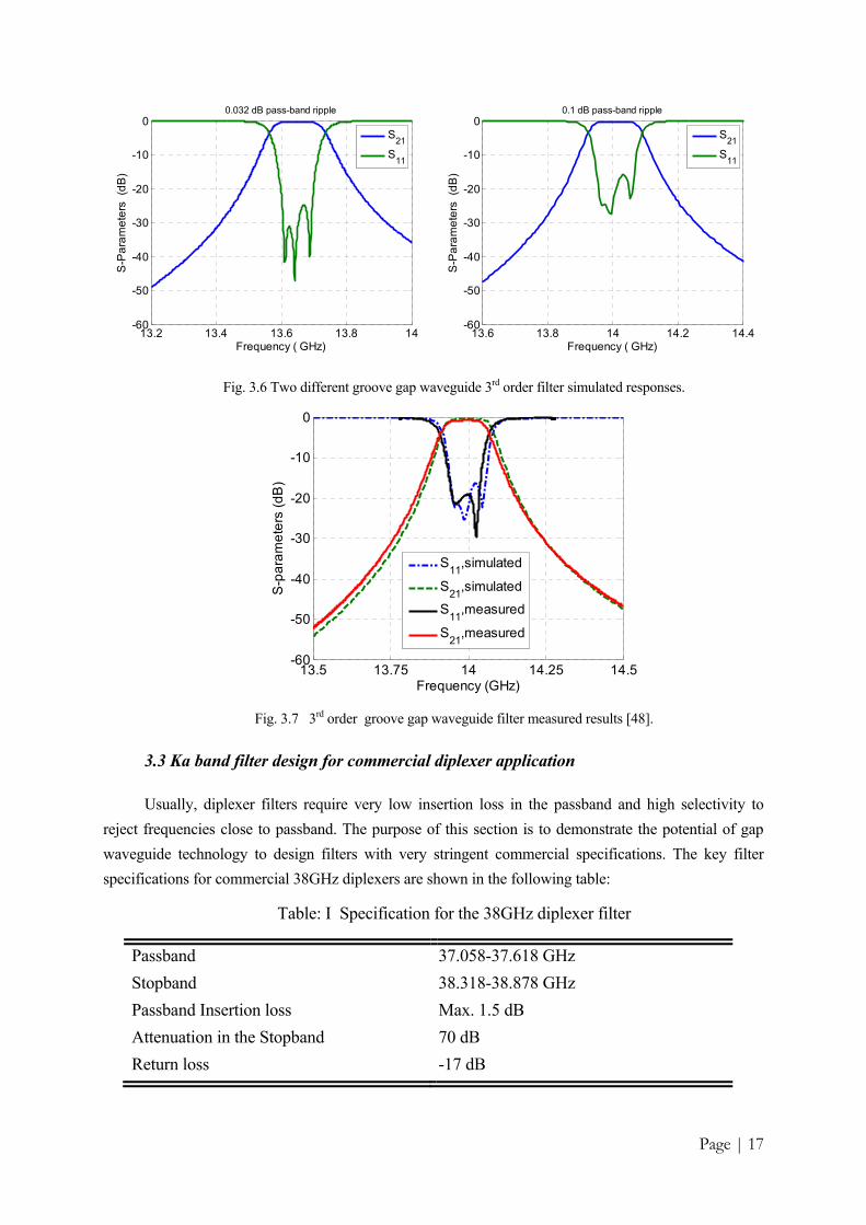
Based on these two coupling mechanisms, 3rd order and 5th order Chebyshev band-pass filters
have been designed at Ku band. The excitation of the input and output resonators of the filters has been
achieved by typical coaxial line using SMA connectors for simplicity of measurements with the help of
available Vector Network Analyzer at Ku band. Two 3rd order filters having 1% relative bandwidth and
pass-band ripple of 0.032dB and 0.1dB are shown in figure 3.5. The simulated results for the two 3rd
order filters are shown in figure 3.6. Out of these two filters, the filter with 0.1dB pass-band ripple has
been manufactured and tested. The measured results are presented in figure 3.7. The details of this filter
design can be found in [48].
Fig. 3.5 Two different groove gap waveguide coupled resonator filters.
Page | 17
Fig. 3.6 Two different groove gap waveguide 3rd order filter simulated responses.
Fig. 3.7 3rd order groove gap waveguide filter measured results [48].
3.3 Ka band filter design for commercial diplexer application
Usually, diplexer filters require very low insertion loss in the passband and high selectivity to
reject frequencies close to passband. The purpose of this section is to demonstrate the potential of gap
waveguide technology to design filters with very stringent commercial specifications. The key filter
specifications for commercial 38GHz diplexers are shown in the following table:
Table: I Specification for the 38GHz diplexer filter
Passband 37.058-37.618 GHz
Stopband 38.318-38.878 GHz
Passband Insertion loss Max. 1.5 dB
Attenuation in the Stopband 70 dB
Return loss -17 dB
13.2 13.4 13.6 13.8 14-60
-50
-40
-30
-20
-10
0
Frequency ( GHz)
S-P
ara
me
ters
(d
B)
0.032 dB pass-band ripple
S21
S11
13.6 13.8 14 14.2 14.4-60
-50
-40
-30
-20
-10
0
Frequency ( GHz)
S-P
ara
me
ters
(d
B)
0.1 dB pass-band ripple
S21
S11
13.5 13.75 14 14.25 14.5-60
-50
-40
-30
-20
-10
0
Frequency (GHz)
S-p
ara
me
ters
(d
B)
S11
,simulated
S21
,simulated
S11
,measured
S21
,measured

prototyp
and the
the low
coupling
followin
To
resonator
chosen a
figure 3.
3.4
Ne
narrow b
coupling
been ach
not need
usually a
at Ka ban
The genera
pe filter to d
coupling to
pass param
g coefficien
ng equations
iK
,
o design the
rs are design
as 2.1mm. Th
8. Details of
Fig. 3.8
4 Summary
ewly introdu
band microw
g mechanism
hieved for m
d any electric
applicable to
nd shows tha
al bandpass
determine th
o the extern
meters are ob
nts (K) and
s:
fracti 1
filter, the ri
ned with pin
he manufactu
this filter are
Ka-band 7th o
uced groove
wave filter w
have been d
manufactured
cal contact be
the standard
at these filters
s filter desi
he required
al circuit; th
btained from
the externa
ig
ig
bandwional
1
idge coupling
n dimension
ured 7th order
e presented in
order groove
gap wavegu
with a fracti
described and
filter structu
etween the sp
d waveguide c
s can meet ve
(dB
)
ign procedu
coupling co
hat is to the
m [51]. Onc
al quality f
width;
g scheme pr
0.7×0.7×2.3
r filter and th
n [52].
gap waveguid
uide technolo
ional bandw
d used to desi
ures even afte
plit blocks an
cavity filters
ery stringent
36-80
-70
-60
-50
-40
-30
-20
-10
0
(dB
)
ure utilizes
oefficients b
e source and
ce the low p
factor (Qex)
frexQ;
esented in se
3 mm3. The
he measured
de filter prototy
ogy is used
width of abou
ign the filters
er removing
nd thus relax
. Also, the m
commercial
36.5 37Fre
the low-pa
between the
d load. For a
pass parame
are easily c
banfractionaln
gn
g
ection 3.2 ha
periodicity
response of t
ype and meas
to design hi
ut 1-2%. Tw
s. Good elect
all the sidew
xes the tight m
measured perf
specification
37.5equency (G
P
ass element
adjacent re
a filter with
eters are kno
calculated b
ndwidth1
ave been cho
of the pins
the filter are
sured results [4
igh Q reson
wo different
trical perform
walls. These
mechanical r
formance for
ns.
38 38.5Hz)
no scre
no scre
screws
screws
Page | 18
ts of the
esonators
h N = 7 ,
own, the
by using
osen. The
has been
shown in
49].
ators and
types of
mance has
filters do
restriction
r the filter
5 39
ews S21
ews S11
s S21
s S11

Page | 19
Chapter4GapWaveguideSlotArrayAntenna
Wireless communication systems have evolved from cellular telephony with data rates of
kilobits per second (kbps) to wireless local area networks (WLANs) and wireless personal area
networks (WPANs) that communicate with megabits per second (Mbps). High-gain and large-aperture
antennas with fixed beams are required to achieve high S/N ratio for point-to-point high-speed systems
(e.g., network backhaul) in the mmWave frequency band.
Although high antenna efficiency can be obtained by using dielectric lens antennas or reflector
antennas [53-56], it is difficult to realize planar structures because they essentially need focal spatial
length. Microstrip array antennas can be light weight, low cost and low profile but they suffer from
high dielectric losses and ohmic losses at high frequency bands [57]. Also, microstrip array antennas
are associated with problems such as leakage via surface waves and undesired radiation [58-59]. Thus,
realization of a high efficiency high gain microstrip antenna array is quite challenging especially at
mmWave frequencies and above.
Slotted hollow waveguide planar array antennas are free from large feed-network loss and can
be applied to design high-efficiency high-gain or moderate-gain antennas [60-61]. However, the
production cost of waveguide antennas is generally very high because they usually consist of metal
blocks with complicated three-dimensional structures. Usually, high precision manufacturing
techniques are needed to achieve good electrical contacts between the slotted metal plate and the
bottom feed structure in such waveguide fed slot array antennas [62]. Apart from the manufacturing
costs and assembly complications, some limitations of waveguide slot arrays have been reported in
literature. Single layer waveguide slot arrays (if the elements are series feed) are simple but have
narrow bandwidth due to long line effect [19]. In single layer structure, it is difficult to feed each
radiating element in parallel (fully corporate-feed) without having the element spacing close to one
wavelength (λo) and avoiding grating lobe issues [63-64]. For wider bandwidth, multilayer antenna
configuration has been considered in [21], [65] which add extra complexity in feed network and
mechanical assembly.
The ridge gap waveguide technology mentioned in the previous sections of this thesis can be used
to design low loss slot array antennas. The low loss feed network needed for an array can be built very
easily with the help of ridge gap waveguide concept. In addition, radiating slots can be placed
conveniently on the top smooth metal plate of ridge gap waveguide. It is possible to design slot antenna
without having strict requirements of good electrical contacts between the slotted metal plate and the
bottom feeding structure. Thus, the ridge gapwaveguide slot antenna with flexible mechanical assembly
can be an attractive as well as cost effective solution for high gain and high efficiency applications. The
corporate feed network (consisting of simple T-junctions) which is a key for wideband slot array
application, can be designed in a fashion similar to that of a microstrip array.

4.1
Th
followed
figure 4.
this desig
slot elem
improved
1 Ridge gap
he slot array
d in this work
1(a). This sin
gn has been
ment are also
d element de
Fig. 4.1(a) Na
Fig. 4.1(b)
p waveguide s
y antenna de
k as well. Th
ngle element
improved w
o varied to
esign and obta
arrow band sl
Wide band sl
slot element
esign usually
he initial sing
t is quite narr
with addition
have the S1
ained reflecti
ot with dimen
ot with T-sect
SW =
and 3-dB po
y starts with
gle slot anten
row band as
of a T-sectio
1 level below
ion coefficien
nsion SL = 11.
coefficient.
tion and its sim
= 5.85mm; TL
11-30
-25
-20
-15
-10
-5
0
S11
(d
B)
11-30
-25
-20
-15
-10
-5
0
S11
(d
B)
ower divider
h a single s
nna excited by
is observed
on ridge [66]
w -10 dB ov
nt for the ele
5mm; SW = 5
mulated reflec
L= 8.25 mm.
12
12
r
lot element.
y ridge gapw
in simulated
]. The length
ver a signifi
ment are sho
.85mm and its
ction coefficie
13
Narrow-band
Frequency (
13
Wide-band
Frequency (
P
Similar app
waveguide is
S11 results.
h and the wid
ficant bandw
own in figure
s simulated re
ent; SL = 11.75
14 15
d Slot
(GHz)
14 15
d Slot
(GHz)
Page | 20
proach is
shown in
Later on,
dth of the
idth. The
4.1(b).
eflection
5mm;
5 16
5 16

Anoth
form of
50Ω line
figure 4.
complete
4.
Ba
been des
spacing
amplitud
11.5-14.5
structure
radiating
contact b
advantag
As ex
first side
the other
on one si
this back
to the sta
interface
wavegui
her importan
a T- junction
es. The ridge
.2. The simu
e array antenn
2 Design of
ased on the a
signed. At th
can be kept
de and phase
5 GHz frequ
e holds the f
g slots at a di
between the
ge of this tech
xpected, the
e-lobe is 11.8
r hand, in E p
ide. In E-plan
k radiation, th
andard transm
e consisting o
de mode (sim
nt componen
n. The T-jun
e waveguide
ulation result
na based on t
Fig. 4.2 S
f linear arra
above mentio
his point, the
t 0.85λ to a
e. The compl
uency band [6
feeding netw
istance of 1 m
radiating lay
hnology.
array has m
8 dB lower fr
plane the bea
ne, there is a
hree corrugat
mission line
of steps in r
milar to that
t for antenna
nction usually
T-junction p
ts show that
this T-junctio
imulated S-pa
ay antenna
oned slot elem
e linear array
avoid grating
lete array is s
67]. As show
work for the
mm from the
yer and botto
more directive
rom the beam
am is wider a
a possibility o
tions are add
for measurem
ridge which
t of standard
a corporate-f
y consists of
power divider
t it is possib
on.
arameters for r
ment and the
y is designe
g lobes and
shown in fig
wn in figure 4
array. On to
e bottom plat
om feed laye
e beam and s
m peak value
and is not rea
of back radiat
ded. It is need
ment of the e
allows the Q
d rectangular
11-30
-25
-20
-15
-10
-5
0
S-P
ara
me
ters
(d
B)
feed network
f a quarter w
r and its sim
ble to design
ridge gap wav
3-dB power
d for a fixed
all the slot
gure 4.3 and
4.3, the botto
op is placed
te. It is impor
er is needed i
symmetric pa
which is als
ally symmetri
tion as the sl
ded also a tra
entire antenn
Quasi TEM m
r waveguide
12
k is the 3-dB
wave transform
mulated S-par
n a wideband
veguide T-junc
divider, a 4×
d beam in m
elements ar
it is designe
m plate with
d a smooth m
rtant to ment
in the array w
attern in H-p
o common fo
ic as the slots
ots are close
ansition from
na. This trans
mode to con
mode). Then
13 14Frequency (
P
B power divid
mer section
rameters are
d feed netw
nction.
×1 linear slot
mind. So, the
re excited w
ed to operate
h ridge and te
metal plate w
tion that- no
which is a s
plane. In H-p
for uniform a
s are close to
to the edge.
m ridge gap w
sition can be
nvert to a gr
en the antenn
15(GHz)
Simula
Simula
Simula
Page | 21
der in the
and three
shown in
ork for a
array has
e element
with equal
e between
exture pin
with four
electrical
ignificant
plane, the
arrays. On
o the edge
To avoid
waveguide
e a simple
roove gap
na can be
16 17
ated S11
ated S21
ated S31

excited
radiation
-40
-35
-30
-25
-20
-15
-10
-5
0
Re
lativ
e L
eve
l (d
B)
with an SM
n patterns in t
Fig
-150 -100
MA connecto
the main plan
Fig. 4.3
Fig. 4
g. 4.5 Measu
11-25
-20
-15
-10
-5
0
S-p
ara
me
ter
(dB
)
-50 0Angle (degre
H -Plane Patte
or with exten
nes are shown
CST model o
4.4 Measured
ured E and H p
11.5 12
50 100 1e)
ern
11G12G13G14G15G
nded inner
n in figure 4.
of the linear a
d and Simulat
plane radiation
2 12.5Frequency
150
GHzGHzGHzGHzGHz
-
-
-
-
-
-
-
Re
lativ
e L
eve
l (d
B)
conductor. T
.4 and figure
array and man
ted S11 for the
n patterns for
13 13.5y (GHz)
S11
S11
-150 -10-40
-35
-30
-25
-20
-15
-10
-5
0
The measure
4.5 respectiv
ufactured arra
e linear array.
r the linear arr
5 14 1
1,measured
1,simulated
00 -50 0Angle (d
E-Plane
P
ed S11 and m
vely.
ay.
ray.
4.5
50 100egree)
Pattern
11GHz12GHz13GHz14GHz15GHz
Page | 22
measured
0 150
zzzzz

4.
Af
gap wav
phase an
frequenc
this parti
bottom p
antenna
coefficie
impedan
3 Design of
fter designin
veguide techn
nd with equa
cy of interest.
icular design
plane using a
and the man
ent and measu
nce bandwidth
f 2×2 eleme
ng the linear
nology to op
al amplitude b
. The slot len
n. The antenn
a transition t
nufactured an
ured principl
h is achieved
Fig. 4.6 C
Fig. 4
11-25
-20
-15
-10
-5
0
S-p
ara
me
ters
(d
B)
ent planar a
array, a simp
perate over th
by a corpora
ngth ‘SL’ and
na is excited
that will be d
ntenna. The
le plane radia
d for this ante
ST model of t
4.7 Measured
12
array antenn
ple 2×2 elem
he band 12-
ate feeding. T
slot width ‘S
with a stand
described in
figure 4.7 an
ation patterns
enna.
the 2×2 eleme
d and simulat
13Freque
na
ment planar ar
15 GHz. The
The element
SW’ are chose
dard Ku-band
chapter 6. F
nd figure 4.8
s respectively
ent array and m
ed S11 for the
14ncy (GHz)
S11
,
S11
,
rray has been
e 2×2 eleme
spacing is a
en to be 11.45
d rectangular
igure 4.6 sho
8 presents the
y. It is eviden
manufactured
planar array.
15
simulated
measured
P
n designed w
ent array is e
about 0.88λ a
5mm and 6.2
r waveguide
ows the mod
e measured r
nt that more t
array.
Page | 23
with ridge
excited in
at highest
25mm for
from the
del of the
reflection
than 20%
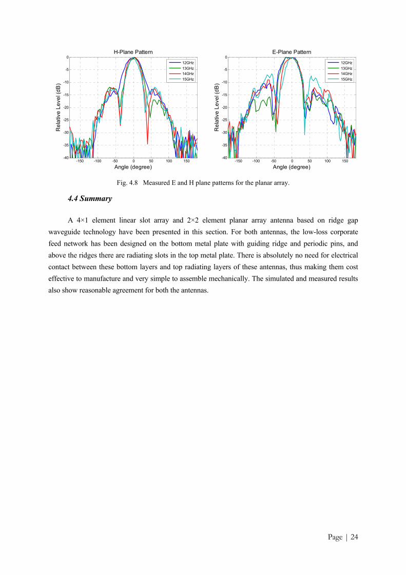
Page | 24
Fig. 4.8 Measured E and H plane patterns for the planar array.
4.4 Summary
A 4×1 element linear slot array and 2×2 element planar array antenna based on ridge gap
waveguide technology have been presented in this section. For both antennas, the low-loss corporate
feed network has been designed on the bottom metal plate with guiding ridge and periodic pins, and
above the ridges there are radiating slots in the top metal plate. There is absolutely no need for electrical
contact between these bottom layers and top radiating layers of these antennas, thus making them cost
effective to manufacture and very simple to assemble mechanically. The simulated and measured results
also show reasonable agreement for both the antennas.
-150 -100 -50 0 50 100 150-40
-35
-30
-25
-20
-15
-10
-5
0
Angle (degree)
Re
lativ
e L
eve
l (d
B)
H-Plane Pattern
12GHz
13GHz14GHz
15GHz
-150 -100 -50 0 50 100 150-40
-35
-30
-25
-20
-15
-10
-5
0
Angle (degree)
Re
lativ
e L
eve
l (d
B)
E-Plane Pattern
12GHz
13GHz14GHz
15GHz

ChaGap
M
and ther
mechani
compactn
into a c
importan
In
substrate
complete
of packa
by the si
significa
waves in
problem
transition
radiation
elements
electrom
also show
In
and redu
effective
used at
overcom
apterpWavMost of mmW
refore have
cal stress and
tness for mm
onfined area
nt in terms of
n a common
e which can c
e circuitry in
age resonance
ignal propaga
ant power lea
n the dielectr
of surface w
ns between d
n or standing
s resulting in
magnetic field
ws the conve
Fig. 5: a)
n practice, the
uction of cros
eness of the t
high frequen
me the packag
5vegui
Wave microwa
to be shield
d environme
mWave micro
a. For such
f isolation and
microwave m
carry the nec
n a metal pac
es and more,
ating in the e
akage exists
ric substrate
wave or PP m
different com
g waves. Th
n interferenc
d coupling an
entional preve
(a)
Various unde
e efficiency
ss-talk goes d
echniques m
ncy and gap
ging related p
idePaave systems
ded, i.e., pa
ental conditio
wave module
high density
d interferenc
module, circ
cessary interc
kage usually
, in general,
electronic circ
on various p
causing seri
mode leakage
mponents or e
his can easily
ce and cross
nd unwanted
ention techni
esired couplin
of the differ
down with fr
mentioned so f
p waveguide
problems.
ackaghave to oper
ackaged in
on. Also, to c
es, large amo
y microwave
ce suppression
cuit compone
connecting lin
y degrades th
due to the in
rcuitry) with
printed circu
ious cross-tal
e and radiatio
even the inter
y get couple
s-talk. Figur
energy leak
iques mention
ng phenomena
rent techniqu
requency; the
far. So, there
e based PMC
gingSrate at outdoo
a proper wa
comply with
ount of electr
e modules, R
n.
ents such as M
nes, the passi
he RF circuit
nteractions of
the package
uit transmissi
lk and interf
on, at mmWa
rconnecting
ed (over the
re 5 displays
kage between
ned in [68-69
a; b) traditiona
ues available
e higher the f
e is a need fo
C packaging
Solutior, under har
ay to provid
the smaller s
ronic compon
RF packagin
MMICS are
ive compone
performance
f electromagn
itself. Publis
ion lines, oft
ference probl
ave frequenc
signal lines m
e air) to the
s some of t
n the adjacent
9].
(b)
al prevention t
for reducing
frequency, th
or new packag
g can be a r
P
ionrsh weather c
de protection
size requirem
nents are to b
ng is more a
placed on a
ents etc. Encl
e because of
netic fields (
shed studies s
ften related t
lems. Apart
cies, intercon
may produce
neighbourin
the possible
nt circuit elem
techniques.
g packaging
he lower is us
aging technol
real good so
Page | 25
conditions
n against
ments and
be placed
and more
dielectric
losing the
the onset
(produced
show that
to surface
from this
nects and
e spurious
ng circuit
ways of
ments and
problems
sually the
ogy to be
olution to

5.
Th
parallel p
surface i
smaller t
microstr
by the ab
of squar
conducto
Th
microstri
the perfo
unwante
above m
several o
substrate
free pack
chain of
geometry
A
advantag
techniqu
several m
the circu
design [7
1 Gap wave
he gap wave
plate cut-off
is a Perfect E
than quarter
rip mode can
bove mentio
re pins (havi
or.
he applicatio
ip line in [70
ormance of w
d cavity mod
mentioned ref
other periodic
e [74] have b
kaging bandw
MMIC is ac
y is studied a
Apart from th
ge while doin
ue, the design
matching laye
uits are practi
76].
eguide pack
eguide packa
f is achieved
Electric Cond
r wavelength
n propagate a
oned PEC-PM
ing height eq
n of gap wav
0]. Later it w
well-known c
des and surfa
ferences, peri
c structures s
een used to o
width is of i
ctive over a v
and this new
he improvem
ng circuit des
ner can reduc
ers. This sav
ically realize
kaging conc
aging solutio
by a Perfec
ductor (PEC)
h. Once a su
along the strip
MC concept.
qual to quar
Fig. 5.1 G
veguide for p
was applied to
oupled line m
ace waves we
iodic pin stru
such as period
obtain the AM
immense inte
very wide fre
geometry off
ments in electr
sign using ful
ce the compu
es computer
d) as the pac
cept
on is based o
ct Magnetic C
) and as long
ubstrate and
p only. Field
As PMC is
rter wavelen
Gap waveguid
packaging wa
o a multi-por
microstrip fil
ere efficiently
uctures have
dic metal spr
MC condition
erest in desig
equency band
fers a very la
trical perform
ll wave simu
utational dom
time and req
ckaging effec
on the conce
Conductor (P
g as the spaci
the microstr
d propagation
not naturally
gth) is used
de packaging c
as first demo
rt antenna fee
ter [72]. In a
y suppressed
e been used t
rings [73] or,
n for such kin
gning multi-
d. In this rega
arge parallel p
mance, this n
lations based
main by using
quires no maj
cts are alread
ept shown in
PMC) surfac
ing between
rip line are p
n in all other
y available, t
to obtain th
oncept.
nstrated succ
ed network in
ll these cases
d within the b
to realize the
, periodic zig
nd of work. A
purpose MM
ard, new inve
plate stop ban
ew packagin
d on FTTD or
g an ideal PM
jor modificat
dy considered
P
n figure 5.1.
ce when the
these two su
placed, the d
r directions i
the periodic
he artificial
cessfully for
n [71] and to
s, it was obse
band of intere
e AMC. But
gzag lines pri
Also, wider r
MICS as the
erted pyrami
nd [75].
ng technique
r FEM. With
MC surface i
tion afterwar
d during the
Page | 26
Here the
opposite
urfaces is
dominant
s stopped
structure
magnetic
a passive
o improve
erved that
est. In the
recently,
inted on a
resonance
complete
dal shape
offers an
h this new
instead of
rds (when
full wave
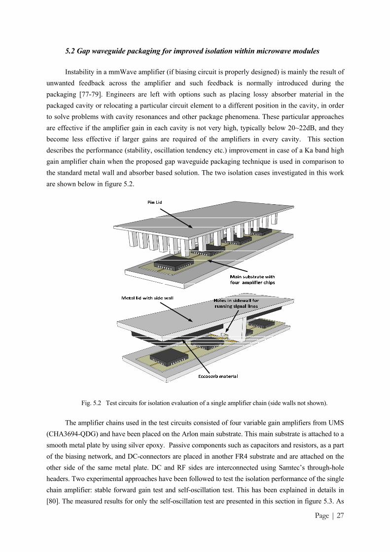
Page | 27
5.2 Gap waveguide packaging for improved isolation within microwave modules
Instability in a mmWave amplifier (if biasing circuit is properly designed) is mainly the result of
unwanted feedback across the amplifier and such feedback is normally introduced during the
packaging [77-79]. Engineers are left with options such as placing lossy absorber material in the
packaged cavity or relocating a particular circuit element to a different position in the cavity, in order
to solve problems with cavity resonances and other package phenomena. These particular approaches
are effective if the amplifier gain in each cavity is not very high, typically below 20~22dB, and they
become less effective if larger gains are required of the amplifiers in every cavity. This section
describes the performance (stability, oscillation tendency etc.) improvement in case of a Ka band high
gain amplifier chain when the proposed gap waveguide packaging technique is used in comparison to
the standard metal wall and absorber based solution. The two isolation cases investigated in this work
are shown below in figure 5.2.
Fig. 5.2 Test circuits for isolation evaluation of a single amplifier chain (side walls not shown).
The amplifier chains used in the test circuits consisted of four variable gain amplifiers from UMS
(CHA3694-QDG) and have been placed on the Arlon main substrate. This main substrate is attached to a
smooth metal plate by using silver epoxy. Passive components such as capacitors and resistors, as a part
of the biasing network, and DC-connectors are placed in another FR4 substrate and are attached on the
other side of the same metal plate. DC and RF sides are interconnected using Samtec’s through-hole
headers. Two experimental approaches have been followed to test the isolation performance of the single
chain amplifier: stable forward gain test and self-oscillation test. This has been explained in details in
[80]. The measured results for only the self-oscillation test are presented in this section in figure 5.3. As

Page | 28
shown in the figure, no oscillation peaks have been observed for gap waveguide packaging (pin lid
packaging) even after 65~70 dB of forward gain. On the other hand, for traditional metal wall packaging
with absorbing material, resonance peaks appeared at around 40dB of total forward gain.
Gap waveguide Packaging Metal wall + absorber
Fig. 5.3 Measured results for self-oscillation test.
5.3 Summary
The gap waveguide technology represents hereby, a new and advantageous way of packaging high
frequency microwave circuits. The performance of the complete microwave system can be destroyed
due to the packaging problems such as cavity resonance, spurious radiation, dominant mode coupling to
substrate modes etc. This chapter clearly shows that- the proposed gap waveguide technology is a very
suitable technology which can overcome the problems of packaging of RF circuits and can improve the
electrical performance of the overall system.
30 31 32 33 34 35 36 37 38 39 40-90
-80
-70
-60
-50
-40
-30
-20
-10
0
Frequency (GHz)
Ou
tpu
t Po
we
r (d
Bm
)
Vcon = -0.40V,(G 20 dB)
Vcon = -0.54V,(G 40 dB)
Vcon = -0.65V,(G 60 dB)
Vcon = -0.70V,(G > 70 dB)
30 31 32 33 34 35 36 37 38 39 40-90
-80
-70
-60
-50
-40
-30
-20
-10
0
Frequency (GHz) O
utp
ut P
ow
er
(dB
m)
Vcon = -0.40V,(G 20 dB)
Vcon = -0.54V,(G 40 dB)
Vcon = -0.65V,(G 60 dB)
Vcon = -0.70V,(G > 70 dB)

Page | 29
Chapter6GapWaveguideTransitions
The transitions between gap waveguide and other standard transmission line such as microstrip
and rectangular waveguide are very important constituent related to gap waveguide components. Most
often, other transmission lines have standardized cross-sections (e.g., rectangular waveguide) or
characteristic impedance (e.g., microstrip line). In order to reduce the reflections from the interface
between gap waveguide and standard transmission lines, impedance transformers or matching sections
are required. This chapter deals with one microstrip to ridge gap waveguide transition and two ridge gap
waveguide to standard rectangular waveguide transitions.
6.1 Microstrip to ridge gap waveguide transition
This transition is based on the fact that the E- field of dominant mode in a microstrip line can be
transformed easily to a standard ridge waveguide mode [81-82]. In case of ridge gap waveguide, it is
even simpler as the dominant mode is also a Quasi-TEM mode. This is shown in figure 6.1.
Fig. 6.1 E-field distributions of dominant mode of microstrip line and ridge gap waveguide.
Due to such similar field distribution, only requirement for a good transition between these two
different transmission lines is an interface for transforming E-fields in the dielectric to E-fields in the air.
This can be done by tapering down the width of the ridge section in several steps. In the proposed design,
the narrower ridge section is viewed as an extended section of the regular ridge section and is placed just
above the microstrip line. The width of the ridge at this section is kept similar to that of the metal strip in
microstrip line. In this way, this tapered ridge section needs to be in electrical contact with the microstrip
line and the substrate. This can be achieved by soldering, gluing or simply by pressing the ridge section
down. In this work, the electric contact is achieved only by mechanical pressure contact. Schematic of
the designed transition between the microstrip line and ridge gap waveguide is shown in figure 6.2. A
standard Chebychev transformer based on several λg/4 sections of different width can also be employed

to impro
to keep t
in figure
transition
loss over
losses of
the entire
M
F
20-25
-20
-15
-10
-5
0
S-p
ara
me
ters
(d
B)
ove the transi
the overall tr
e 6.3. The me
n will have e
r the same 23
f the ridge ga
e Ka band.
Microstrip line
Fig. 6.2 Schem
Fig. 6.3
0 25
ition. But in t
ransition com
easured retur
even lower r
3-43 GHz ba
ap waveguide
ExtendedSectio
Su
matic details o
Manufacture
30Frequency (
this work, on
mpact. The m
rn loss is 14.
eturn loss ov
and is found
e section mea
Ridge on
Back to BTransiti
rrounding Pnot sh
of the proposed
ed back-to-bac
35 40(GHz)
nly one taper
manufactured
.15 dB for th
ver the entire
to be 0.32 dB
aning a loss
Metal Pins
Back on
Pins along thhown in uppe
d transition, W
= 2.75 mm.
ck transition an
45
S21
S11
red section of
transition an
he 23-43 GH
e Ka band of
B for the bac
smaller than
Shheig
e exteded seer two views
y
W1 = 2.65 mm,
nd measured S
f the ridge ha
nd the measu
Hz band whic
f interest. Th
ck-to-back tr
0.16 dB per
w1
w2
orter ht pins
ection are s
W2 = 0.72 mm
S-parameters f
P
as been used
ured results a
ch means tha
he maximum
ransition incl
r single transi
x
b
m, x = y = 20 m
for the transitio
Page | 30
d in a way
are shown
at a single
insertion
uding the
ition over
mm and b
on.

Page | 31
6.2 Ridge gap waveguide to rectangular waveguide transition
Two transitions from ridge gap waveguide to rectangular waveguide have been designed recently.
One is the inline transition where the height of the guiding ridge is reduced in several steps to match the
height of the empty rectangular waveguide. In the other transition, the ridge gap waveguide is excited by
a rectangular waveguide from the bottom. The first transition with stepped ridge sections is designed at
Ka-band and is shown in figure 6.4 where the critical dimensions are as follows: L1 = 2.46mm; L2 =
2.27mm; L3 = 2.17mm; L4 = 1.78mm and S1= 0.22mm; S2= 0.52mm; S3= 0.76mm, S4 = 0.53mm and S5=
0.42mm. The simulated performance of this back to back transition is shown in figure 6.5. We can
observe a good performance in the whole waveguide band.
Fig. 6.4 Back-to-back transition with stepped ridge section, top metal plate not shown here.
Fig. 6.5 Simulated S-parameters for the stepped ridge back-to-back transition.
The other transition is also a simple transition where the rectangular waveguide is feeding the ridge
gap waveguide from the bottom. This type of transition is needed for measuring the ridge gap waveguide
antenna where the feeding waveguide has to be placed below the antenna. The transition is designed at
25 30 35 40-45
-40
-35
-30
-25
-20
-15
-10
-5
0
Frequency (GHz)
S-p
ara
me
ters
(d
B)
Simulated,S11
Simulated,S21

Page | 32
Ku-band and is shown in figure 6.6 where all critical dimensions for this transition are as follows: PL =
3.65mm; Pw = 1.25mm; Ps = 4.25mm; Rw = 4mm; R = 2mm. The simulated performance of the single
transition is shown in figure 6.7.
Fig. 6.6 Ridge gap waveguide to rectangular waveguide transition (fed from bottom).
Fig. 6.7 Simulated S-parameters for the single transition of ridge gap waveguide to rectangular waveguide
(fed from bottom).
6.3 Summary
Three important transitions have been presented in this chapter. The microstrip to ridge gap
waveguide transition has been manufactured and measured. The other two ridge gap waveguide to
rectangular waveguide transitions have been used in the two ridge gap waveguide slot array antenna
presented in chapter four. All these transitions worked over considerable bandwidth and measured results
remain within acceptable limits and are in reasonable agreement with the simulated results.
12 13 14 15 16 17 18-35
-30
-25
-20
-15
-10
-5
0
Frequency (GHz)
S-p
ara
me
ters
(d
B)
Simulated,S11
Simulated,S21
Page | 33
Chapter7Conclusionandfuturework
To leverage the vast unlicensed bandwidth available at mmWave frequencies, wireless and
microwave designers have begun developing high frequency system architectures, circuits, antennas and
packages. But as expected, they face enormous challenges to design, develop and integrate components
cost effectively. As for example, a simple interconnect that works very well at 5GHz may have
unacceptable loss above 60GHz and can become a source of unwanted radiation. Due to the increasingly
short wavelengths, power dissipated along straight lines can be of lesser importance in comparison to the
influence of discontinuities that become electrically large and cause reactance, radiation and excitation of
surface waves. Also, power generation at these high frequencies is difficult and designers cannot afford
this hard-fought-for RF power to lose in interconnects, discontinuities or components. Thus, the
challenges are many at mmWave frequencies, making this an incredibly rich and deep area of research in
the coming years. Surely, microwave engineers will come up with streams of new concepts, ideas and
technologies around all the problem areas and will reinvent the wireless industry.
The gap waveguide technology presented in this thesis is a similar new concept with lots of
potential in it to be used at high frequency spectrum. It is much lower loss than microstrip or CPW and
has very flexible mechanically assembly compared to metal waveguide. It also solves the difficult
problems of unwanted radiation, excitation of surface waves, cavity modes and isolation and can easily
be applied for packaging high frequency modules and circuits. In fact, this new technology can be used
to design all critical passive components (e.g., filters, antennas etc.) and the packaging lid for the active
circuits in a single module. This single unit will become a more robust and compact module providing
improved electrical performance, reduced cost and will cause less delay in production chain.
The scope of this dissertation focuses on the gap waveguide passive components and packaging
solutions for RF front-ends. This thesis deals mainly with ridge gap and groove gap waveguide and uses
periodic metal pins as AMC surface. Major contributions from this work can be summarized as follows:
Firstly, validation of gap waveguide concept has been done by designing and manufacturing
first ridge gap waveguide demonstrator. Theoretical and experimental work has been done to
confirm the low loss property of the first demonstrator by designing in house TRL
calibration kit and characterizing losses of ridge gap waveguide. For such oversized parallel
plate structures, the level of field attenuation in the periodic structure is very significant.
This field attenuation has been carefully investigated and measured for gap waveguide
structures.
Secondly, narrow band filters with high selectivity have been designed at Ku-band and Ka-
band based on groove gap waveguide technology. Good electrical performance is achieved
for manufactured high Q filter structures even after removing the sidewalls. Two different

Page | 34
types of coupling mechanisms have been investigated and used to design these filters. For
these groove gap waveguide filters, the spit-block assembly is not critical at all, thus making
these filters much more flexible to manufacture and integrate with other critical components
such as antennas.
Thirdly, planar slot array antennas have been designed as a proof of concept for gap
waveguide based high gain antenna. Initially, a wideband single slot element has been
developed. Later on, a 4×1 element linear array and a 2×2 element planar array have been
designed and manufactured at Ku-band as a demonstrator. These two slot array antennas
work over 20% of relative bandwidth. Both the antennas have the feeding network in the
bottom metal plate consisting of guiding ridge and periodic pins, and above the ridges there
are radiating slots in the top metal plate. Thus, these antennas have very simple single layer
feeding network which is of great advantage considering the mechanical assembly and
manufacturing complexity of the 3-D structure.
Fourthly, the parallel-plate mode suppression quality of gap waveguide technology is
applied in microwave modules to package microstrip circuits. By using the gap waveguide
package, many critical package related phenomena such as onset of cavity modes, leakage
to substrate modes, radiation from discontinuity, feedback issue due to over the air coupling
etc. have been prevented within the band of interest. Gap waveguide packaging technique
has been successfully utilized to improve the performance of passive circuits such as
microstrip filters and active amplifier chains yielding high forward gain. The main
advantage of the proposed packaging technique is that- it is scalable to any frequency range.
Also, packaging performance does not depend on mechanical issues such as stress and
corrosion, joint reliability, surface properties, and deformations or apertures caused by
thermal expansions or contractions.
Lastly, transitions between ridge gap waveguide and other standard transmission lines such
as microstrip and rectangular waveguide have been designed and tested. The microstrip to
ridge gap waveguide transition has a compact design with a transformation of EM fields
from typical microstrip mode to air-filled ridge gap waveguide mode. The transition works
even without soldering which is quite an advantage in some systems where large number of
transitions is needed in separable modules or split-blocks. On the other hand, one of the
ridge gap waveguide to rectangular waveguide transition is a typical inline transition where
the height of the guiding ridge is reduced in several steps to match the height of the empty
rectangular waveguide. In the second transition, the ridge gap waveguide is excited by a
rectangular waveguide from the bottom which is very suitable for antenna measurements.
In summary, this research work lays the foundation for promoting and investigating the gap
waveguide technology for the development of a broad range of high frequency and mmWave devices or
systems. This dissertation will help in exploration and development of future generation high-volume
and mass-producible high frequency microwave components based on gap waveguide technology.

Page | 35
Future work
Following the work and studies described in this dissertation, a number of technical issues are still
waiting to be resolved. Some of these issues are mentioned below:
The work presented in the thesis serves as a proof of concept for gap waveguide technology
and its potential, but its applications in the field of mmWave frequency or even higher
frequency wireless systems need more system level evaluation. More efforts will be needed to
accomplish a well-developed academic/industrial project.
This thesis mainly deals with ridge gap waveguide and groove gap waveguide technology. The
potential of microstrip gap waveguide technology needs to be investigated more at high
frequency and mmWave frequency range.
High frequency active components need to be integrated in a good way with the gap
waveguide structures to exploit the full benefit of this technology. New wideband transition
design is necessary to be able to do so.
Fabrication tolerances associated with commonly used CNC milling or molding techniques
have to be investigated more in depth to realize the gap waveguide components at mmWave
frequency range. Apart from the fabrication tolerance issue, the conductor losses for gap
waveguide have to be characterized well at mmWave frequency, in particular, for frequency
ranges where the skin depth is comparable with the surface roughness.
Fabrication techniques such as silicon based micromachining have been tried recently for
realizing gap waveguide structures at a frequency of 100 GHz and above [83-84]. However,
there are other manufacturing techniques such as laser milling and 3D printing process in
metal, etc. These fabrication techniques can also be suitable for realizing high frequency gap
waveguide structures and needs more thorough investigation.

Bibliography
[1] Lockie and D. Peck, “High-data-rate millimeter-wave radios,” IEEE Microwave Mag.,
vol. 10, no. 5, pp. 75–83, Aug. 2009.
[2] J. Wells, “Faster than fiber: The future of multi-G/s wireless,” IEEE Microwave Mag.,
vol. 10, no. 3, pp. 104–112, May 2009.
[3] J. Hasch, E. Topak, R. Schnabel, T. Zwick, R. Weigel, and C. Waldschmidt, “Millimeter-
wave technology for automotive radar sensors in the 77 GHz frequency band,” IEEE
Trans. Microw. Theory Tech., vol. 60, no. 3, pp. 845–860, Mar. 2012.
[4] Y.-C. Ou and G. M. Rebeiz, “On-chip slot-ring and high-gain horn antennas for
millimeter-wave wafer-scale silicon systems,” IEEE Trans. Microw. Theory Tech., vol.
59, no. 11, pp. 1963–1972, Aug. 2011.
[5] H. Kaouach, L. Dussopt, J.Lantéri, T. Koleck, R.Sauleau, “Wideband Low-Loss Linear and
Circular Polarization Transmit-Arrays in V-Band,” IEEE Trans. on Antennas and Propag.,
vol: 59, no.7, pp. 2513 - 2523, July 2011.
[6] J. W. Waters et al., “The Earth Observing System Microwave Limb Sounder (EOS MLS)
on the Aura satellite,” IEEE Trans. Geosci. Remote Sens., vol. 44, no. 5, pp. 1075–1092,
May 2006.
[7] K. B. Cooper, R. J. Dengler, N. Llombart, T. Bryllent, G. Chattopadhyay, E. Schlecht, J.
Gill, C. Lee, A. Skalare, I. Mehdi, and P. H. Siegel, “Penetrating 3-D imaging at 4- and
25-m range using a submillimeter- wave rader,” IEEE Trans. Microw. Theory Tech., vol.
56, no. 12, pp. 2771–2778, Dec. 2008.
[8] K. Wu, Y. J. Cheng, T. Djerafi, and W. Hong, “Substrate-integrated millimeter-wave and
terahertz antenna technology,” Proc. IEEE, vol. 100, no. 7, pp. 2219–2232, Jul. 2012.
[9] X. Shang, M.Ke Y.Wang, M.J. Lancaster, “Micromachined W-band waveguide and filter
with two embedded H-plane bends,” IET Microwaves, Antennas and Propag., vol. 5, Iss.3,
pp-334-339, 2011.
[10] J.P. Becker, J.R. East, L.P.B. Katehi, “Performance of silicon micromachined waveguide
at W-band,” Electronic Letters, vol.38, no.13, pp- 638-639, June 2002.
[11] M. Zhang, J. Hirokawa and M. Ando, “An E-Band Partially Corporate Feed Uniform
Slot Array With Laminated Quasi Double Layer Waveguide and Virtual PMC
Terminations,” IEEE Trans. Antennas and Propag., vol. 59, no. 5, pp. 1521-1527, May
2011.
[12] Carlos Vicente and Hans L. Hartnagel, “Passive Intermodulation Analysis Between
Rough Rectangular Waveguide Flanges”, IEEE Trans. Microw. Theory and Tech., vol. 53,
no.8, pp. 2515 - 2525, August 2005.

[13] M. Tsuji, H. Shigesawa, and A.A. Oliner, “Simultaneous Propagation of bound and leaky
dominant modes on printed-circuit lines,” IEEE Trans. Microw. Theory and Tech., vol. 43,
no. 12, pp. 3007-3019, December 1995.
[14] F. Mesa, A. A. Oliner, D. R. Jackson, and M. J. Freire, “The influence of a top cover on
the leakage from microstrip line,” IEEE Trans. Microw. Theory and Tech., vol. 48, no. 12,
pp. 2240-2248, December 2000.
[15] W.E.McKinzie and N.G. Alexopoulos, “Leakage losses for the dominant mode of
conductor-backed coplanar waveguide,” IEEE Microwave Guided Wave Letter, vol. 2, pp.
65-66, February 1992.
[16] S.-J. Kim, H.-S. Yoon, and H.-Y. Lee, “Suppression of leakage resonance in coplanar
MMIC packages using a Si sub-mount layer, ” IEEE Trans. Microwave Theory Tech., vol.
48, no. 12, pp. 2664-2669, December 2000.
[17] P. S. Hall and C. M. Hall, “Coplanar corporate feed effects in microstrip patch array
design,” Proc. Inst. Elect. Eng., pt. H, vol. 135, pp. 180–186, June 1988.
[18] E. Levine, G. Malamud, S. Shtrikman, and D. Treves, “A study of microstrip array
antennas with the feed network,” IEEE Trans. Antennas and Propag., vol. 37, no. 4, pp.
426–434, Apr. 1989.
[19] S. Park, Y. Tsunemitsu, J. Hirokawa, and M. Ando, “Center feed single layer slotted
waveguide array,” IEEE Trans. Antennas and Propag., vol. 54, no. 5, pp. 1474–1480,
May 2006.
[20] M. Ando, Y. Tsunemitsu, M. Zhang, J. Hirokawa, and S. Fujii, “Reduction of long line
effects in single-layer slotted waveguide arrays with an embedded partially corporate
feed,” IEEE Trans. Antennas and Propag., vol. 58, no. 7, pp. 2275–2280, Jul. 2010.
[21] Y. Miura, J. Hirokawa, M. Ando, Y. Shibuya, and G. Yoshida, “Double-layer full-
corporate-feed hollow-waveguide slot array antenna in the 60 GHz-band,” IEEE Trans.
Antennas and Propag., vol. 59, no. 8, pp. 2844–2851, Aug. 2011.
[22] Daniel G.Swanson, Jr., “Narrow-Band Microwave Filter Design,” IEEE Microwave
Magazine, pp.105-114, October 2007.
[23] R. Levy and S. B. Cohn, “A history of microwave filter research, design, and
development,” IEEE Trans. Microwave Theory Tech., vol. 32, no. 9, pp. 1055–1067,
Sept. 1984.
[24] G. L. Matthaei, L. Young, and E. M. T. Jones, Microwave Filters, Impedance-
Matching Networks, and Coupling Structures. Dedham, MA: Artech House, 1980.
[25] D. Deslandes and K. Wu, “Integrated microstrip and rectangular waveguide in planar
form,” IEEE Microwave Wireless Compon. Lett., vol. 11, no. 2, pp.68 -70, November
2001.
[26] F. Xu and K. Wu, “Guided-wave and leakage characteristics of substrate integrated
waveguide,” IEEE Trans. Microw. Theory Tech., vol. 53, no. 1, pp. 66–73, Jan. 2005.

[27] K. Wu, “Towards System-on-Substrate approach for future millimeter-wave and
photonic wireless applications,” In Proc. Of Asia-Pacific Microwave Conference, 2006.
[28] G. Six, G. Prigent, E. Rius, G. Dambrine, and H. Happy, “Fabrication and
characterization of low-loss TFMS on silicon substrate up to 220 GHz,” IEEE Trans.
Microw. Theory Tech., vol. 53, no. 1, pp. 301–305, Jan. 2005.
[29] K. Nishikawa, S. Sugitani, K. Inoue, T. Ishii, K. Kamogawa, B. Piernas, and K. Araki,
“Low loss passive components on BCB-based 3-D MMIC technology,” in IEEE MTT-S
Int. Microwave Symp. Dig., May 2001, pp.1881–1884.
[30] M.F. Shafique, and I.D. Robertson, “Laser prototyping of multilayer LTCC microwave
components for system-in-package applications,” IET Microwaves Antennas &
Propagation, vol.5, issue.8, pp.864, 2011.
[31] T.-M. Shen, C.-F. Chen, T.-Y. Huang, and R.-B.Wu, “Design of vertically stacked
waveguide filters in LTCC,” IEEE Trans. Microw. Theory Tech., vol. 55, no. 8, pp.
1771–1779, Aug. 2007.
[32] P.-S. Kildal, E. Alfonso, A. Valero-Nogueira, E. Rajo-Iglesias, “Local metamaterial-
based waveguides in gaps between parallel metal plates,” IEEE Antennas and Wireless
Propag. Letters, vol. 8, pp. 84-87, 2009.
[33] P.-S. Kildal, A. Uz Zaman, E. Rajo-Iglesias, E. Alfonso and A. Valero-Nogueira,
“Design and experimental verification of ridge gap waveguides in bed of nails for parallel
plate mode suppression,” IET Microwaves, Antennas & Propagation, vol.5, issue.3, pp.
262-270, March 2011.
[34] P.-S. Kildal, “Artificially soft and hard surfaces in electromagnetics,” IEEE Trans.
Antennas and Propagation, vol. 38, no. 10, pp. 1537-1544, Oct. 1990.
[35] M.G. Silveirinha, C.A.Fernandes and J.R. Costa, “Electromagnetic characterization of
textured surfaces formed by metallic pins, ” IEEE Trans. Antennas and Propag., vol. 56,
no. 2, pp. 405-415, February 2008.
[36] D.Sievenpiper, L.Zhang, R.F.J.Broas, N.G.Alexopolous, and E. Yablonovitch, “High-
impedance electromagnetic surfaces with a forbidden frequency band, ” IEEE Trans.
Microwave Theory Tech., vol. 47, no. 11, pp. 2059-2074, November 1999.
[37] P.-S. Kildal, “Three metamaterial-based gap waveguides between parallel metal plates for
mm/submm waves”, 3rd European Conference on Antennas and Propagation, Berlin,
March 2009.
[38] A. Valero-Nogueira, E. Alfonso, J. I. Herranz, P.-S. Kildal, “Experimental demonstration
of local quasi-TEM gap modes in single-hard-wall waveguides,” IEEE Microwave and
Wireless Components Letters, vol. 19, no.9, pp. 536-538, 2009.
[39] A. Valero-Nogueira, J. Domenech, M. Baquero, J. I. Herranz, E. Alfonso, and A. Vila,
“Gap waveguides using a suspended strip on a bed of nails,” IEEE Antennas and Wireless
Propag. Letters, vol.10, pp. 1006-1009, 2011.
[40] E. Pucci, E. Rajo-Iglesias and P.-S. Kildal, “Gap waveguides using a suspended strip on
a bed of nails,” IEEE Microwave and Wireless Comp. Letters, vol.22, no.3, pp. 129-131,
2012.
[41] E. Rajo-Iglesias and P.-S. Kildal, “Groove Gap Waveguide: A Rectangular Waveguide
between Contactless Metal Plates Enabled by Parallel-Plate Cut-Off,” Proceedings of 4th
European Conference on Antennas and Propagation, April 2010.
[42] E. Rajo-Iglesias and P.-S. Kildal, “Numerical studies of bandwidth of parallel plate cut-
off realized by bed of nails, corrugations and mushroom-type EBG for use in gap wave-
guides,” IET Microw., Antennas & Propag., vol.5, issue.3, pp. 282-289, March 2011.
[43] A. Uz Zaman, E. Rajo-Iglesias, E. Alfonso, P.-S. Kildal, ‘Design of transition from
coaxial line to ridge gap waveguide,” IEEE Antennas and Propagation Society
International Symposium, June 2009.
[44] Glenn F. Engen, Cletus A. Hoer, “Thru-Reflect-Line: An improved technique for
calibrating the dual six port automatic network analyzer,” IEEE Trans.on Microw. Theory
and Tech., vol.27, no.12, pp. 987-993, December 1979.
[45] Renato R. Pantoja, Michel J. Howes, John R. Richardson, Roger D. Pollard, “Improved
Calibration and Measurement of the Scattering parameters of microwave integrated
circuits,” IEEE Trans.on Microw. Theory and Tech., vol.37, no.11, pp. 1675-1680,
November 1989.
[46] Ian C.Hunter, L.Billonet, Bernard Jarry and Pierre Guillon, “Microwave Filters-
Applications and Technology,” IEEE Trans. Microw. Theory and Tech., vol. 50, no. 3, pp.
794-804, March 2002.
[47] S. B. Cohn, “Direct-coupled resonator filters,” Proc. IRE, vol. 45, pp.187–196, Feb. 1957.
[48] A. Uz Zaman, P.-S. Kildal, and A.Kishk, “Narrow-Band Microwave Filter Using High
Q Groove Gap Waveguide Resonators with Manufacturing Flexibility and no Sidewalls,”
IEEE Transactions on Components, Packaging and Manufacturing Technology, vol.2,
no-11, pp- 1882-1888, November, 2012.
[49] J. Uher, J. Bornemann, and U. Rosenberg, Waveguide Components for Antenna Feed
Systems: Theory and CAD. Norwood, MA: Artec House, 1993.
[50] E. Pucci, A.Uz.Zaman, E. Rajo-Iglesias, P.-S. Kildal and A.Kishk “Study of Q factors
of Ridge and Groove Gap Waveguide Resonator,” Submitted to IET Microwaves,
Antennas & Propagation.
[51] J-S. Hong, M.J Lancaster, Microstrip Filters for RF/Microwave Applications, Wiley-
Interscience Publication, ISBN: 047138877-7, 2001.
[52] E. Alfonso, A. Uz Zaman and P.-S. Kildal, “Ka-Band Gap Waveguide Coupled-
Resonator Filter for Radio Link Diplexer Application,” Accepted for publication in IEEE
Transactions on Components, Packaging and Manufacturing Technology.

[53] B. Chantraine-Barès and R. Sauleau, “Electrically-Small Shaped Integrated Lens
Antennas: A Study of Feasibility in Q-Band,” IEEE Trans. Antennas and Propag., vol.
55, no. 4, pp. 1038–1044, April 2007.
[54] L. Mall and R. B. Waterhouse, “Millimeter-wave proximity-coupled microstrip antenna
on an extended hemispherical dielectric lens,” IEEE Trans. Antennas and Propag., vol.
49, no. 12, pp. 1769–1772, Dec. 2001.
[55] P.-S. Kildal, “The hat feed: A dual-mode rear-radiating waveguide antenna having low
cross polarization,” IEEE Trans. Antennas and Propag., vol. 35, no. 9, pp. 1010–1016,
Sep. 1987.
[56] W. Wei, J. Yang, T. Ostling, and T. Schafer, “A new hat feed for reflector antennas
realized without dielectrics for reducing manufacturing cost and improving reflection
coefficient,” IET Microwaves, Antennas & Propag., vol. 5, no. 7, pp. 837–843, Jul. 2011.
[57] A. Borji, D. Busuioc and S. Safavi-Naeini, “Efficient, Low-Cost Integrated Waveguide-
Fed Planar Antenna Array for Ku-Band Applications,” IEEE Antennas and Wireless
Propag. Letters, vol.8, pp.336–339, 2009.
[58] D M. Pozar, “ Considerations for Millimeter Wave Printed Antennas,” IEEE Trans. on
Antennas and Propag., vol.31, no.5, pp.740–747, September 1983.
[59] E.Levine, G. Malamud, S.Shtrikman and D. Treves, “A study of microstrip array
antennas with the feed network,” IEEE Trans. on Antennas and Propag., vol.37, no.4,
pp.426–464, April 1989.
[60] J. Hirokawa and M. Ando, “Single-layer feed waveguide consisting of posts for plane
TEM wave excitation in parallel plates,” IEEE Trans. Antennas Propag., vol. 46, no. 5,
pp. 625–630, May 1998.
[61] J. Hirokawa and M. Ando, “Efficiency of 76 GHz Post-wall Waveguide-fed Parallel-
plate Slot Arrays,” IEEE Trans. Antennas Propag., vol. 48, no. 11, pp. 1742-1745,
November 2000.
[62] YKimura, T.Hirano, J.Hirokawa and M.Ando, “Alternating-phase fed single-layer
slotted waveguide arrays with chokes dispensing with narrow wall contacts,” IEE Proc.-
Microw. Antennas Propag , vol. 148, no.5, October 2001.
[63] S. Fujii, Y. Tsunemitsu, G. Yoshida, N. Goto, M. Zhang, J. Hirokawa, and M. Ando,
“A wideband single-layer slotted waveguide array with an embedded partially corporate
feed,” in Proc. Int. Symp. Antennas & Propag., TP-C27-5, Oct. 2008.
[64] T. Tsugawa, Y. Sugio, and Y. Yamada, “Circularly polarized dielectric- loaded planar
antenna excited by the parallel feeding waveguide network,” IEEE Trans. Broadcasting,
vol. 43, no. 2, pp. 205–212, June 1997.
[65] H. Kirino and K. Ogawa, “A 76 GHz Multi-Layered Phased Array Antenna Using a Non-
Metal Contact Metamaterial Waveguide,” IEEE Transactions on Antennas and Propag.,
vol. 60, no. 2, pp. 840-853, February 2012.

[66] A. Uz Zaman and P.-S. Kildal, “Slot Antenna in Ridge Gap Waveguide Technology,”
6th European Conference on Antennas and Propagation, Prague , March, 2012.
[67] A. Uz Zaman and P.-S. Kildal, “Ku-Band Linear Slot-Array in Ridge Gapwaveguide
Technology,” 7th European Conference on Antennas and Propagation, Gothenburg ,
April, 2013.
[68] Dylan F. Williams, “Damping of the Resonant Modes of Rectangular Metal Package,”
IEEE Trans. Microw.Theory and Tech. vol. 37, no.1, pp. 253 - 256, January 1989.
[69] Paul Dixon, “Cavity Resonance Damping,” IEEE Microwave Magazine, pp. 1 - 7, June
2005.
[70] E. Rajo-Iglesias, A. Uz Zaman, P.-S. Kildal, “Parallel plate cavity mode suppression in
microstrip circuit packages using a lid of nails,” IEEE Microwave and Wireless Com-
ponents Letters, vol. 20, no. 1, pp. 31-33, Dec. 2009.
[71] A.Uz Zaman, J.Yang and P.-S. Kildal, “Using Lid of Pins for Packaging of Microstrip
Board for Descrambling the Ports of Eleven Antenna for Radio Telescope Applications,”
IEEE Antennas and Propagation Society International Symposium, 2010.
[72] A. Algaba Brazález, A. Uz Zaman, and P.-S. Kildal, “Improved Microstrip filters Using
PMC Packaging by Lid of Nails,” IEEE Trans. Component,Packaging and Manufacturing
Technology, vol. 2, no. 7, pp. 1075-1084, July 2012.
[73] E. Rajo-Iglesias, A.Kishk , A. Uz Zaman and P.-S. Kildal, “Bed of Springs for Packaging
of Microstrip Circuits in the Microwave Frequency Range,” IEEE Trans.
Component,Packaging and Manufacturing Technology, vol. 2, no. 10, pp. 1623-1628,
October,2012.
[74] E. Rajo-Iglesias, E. Pucci, A.Kishk and P.-S. Kildal, “ Suppression of parallel plate
modes in low frequency microstrip circuit packages using lid of printed zigzag wires,”
Submitted to IEEE Microwave and Wireless Components Letters
[75] A.Uz Zaman, V.Vassilev, P.-S. Kildal, A. Kishk, “Increasing Parallel Plate Stop-band
in Gap Waveguides using Inverted Pyramid-Shaped Nails for Slot Array Application
Above 60GHz,” The 5th European Conference on Antennas and Propagation, Rome,
April 2011.
[76] A. Kishk, A. Uz Zaman,and P.-S. Kildal, “Numerical Prepackaging with PMC lid -
Efficient and Simple Design Procedure for Microstrip Circuits including the Packaging,”
ACES Applied Computational Society journa, vol. 27, no. 5, pp. 389-398, May 2012.
[77] S. Weinreb, P. C. Chao, and W. Copp, “Full-waveguide band, 90 to 140 GHz MMIC
Amplifier module,” IEEE MTT-S Int Microwave Symp., pp. 1279-1280, June 1997.
[78] W. H. Haydl, “Resonance phenomena and power loss in conductor- backed coplanar
structures, ” IEEE Microwave Guided Wave Letter, vol. 20, pp. 514-516, December 2000.
[79] M.A.Morgan, “Millimeter-wave MMICs and Applications,” Ph.D. dissertation,
California Institute of Technology, Pasadena, California, 2003.

[80] A.Uz Zaman, M. Alexanderson, T. Vukusic, P.-S. Kildal, “Gap Waveguide PMC
Packaging For Improved Isolation of Circuit Components in High Frequency Microwave
Modules,” Submitted to IEEE Trans. Component,Packaging and Manufacturing
Technology.
[81] H.-W. Yao, A. Abdelmonem, J.-F. Liang, and K. A. Zaki, “Analysis and design of
microstrip-to-waveguide transitions,” IEEE Trans. Microw. Theory and Tech., vol. 42, no.
12, pp. 2371–2380, Dec. 1994
[82] Y. Zhang, J. A. Ruiz-Cruz, K. A. Zaki and A. J. Piloto, “A Waveguide to Microstrip
Inline Transition With Very Simple Modular Assembly,” IEEE Microwave and Wireless
Components Letters, vol. 20, no.9, September 2010.
[83] S. Rahiminejad, A.U. Zaman, E. Pucci, H. Raza, V. Vassilev, S. Haasl, P. Lundgren, P.-S.
Kildal and P. Enoksson, “Micromachined ridge gap waveguide and resonator for
millimeter-wave applications,” Elsevier, Sensors and Actuators A: Physical, vol. 186, pp.
264-269, October 2012.
[84] S. Rahiminejad, H. Raza, A. Uz Zaman, S. Haasl, P. Enoksson and P.-S. Kildal,
“Micromachined Gap Waveguides for 100GHz Applications,” 7th European Conference
on Antennas and Propagation, Gothenburg , April, 2013.
[85] J.T.Gear, ‘‘Microwave absorbers manage military electronics RF interference’’, RF
Design, pp.6-9, August 2004.
[86] A. Uz Zaman, P.-S. Kildal, M. Ferndahl and A. kishk, “Validation of Ridge
Gapwaveguide Performance by Using In-house TRL Calibration Kit ,” 4th European
Conference on Antennas and Propagation, Barcelona , April, 2010.


![Literaturverzeichnis - · © Springer-Verlag 2006 Literaturverzeichnis [Ale00] Gerald L. Alexanderson: The random walks of George Pólya, Mathema- tical Association of](https://img.pdfslide.us/doc/110x75/5fc3a33006361b15223baa58/literaturverzeichnis-springer-verlag-2006-literaturverzeichnis-ale00-gerald.jpg)