Embed Size (px)
Citation preview

Microtubes decorated with nanowiresC. M. Rivaldo-Gómez, A. Zúñiga, D. Criado, J. Schoenmaker, and J. A. Souza Citation: Applied Physics Letters 106, 213104 (2015); doi: 10.1063/1.4921795 View online: http://dx.doi.org/10.1063/1.4921795 View Table of Contents: http://scitation.aip.org/content/aip/journal/apl/106/21?ver=pdfcov Published by the AIP Publishing Articles you may be interested in A ZnO nanowire resistive switch Appl. Phys. Lett. 103, 123114 (2013); 10.1063/1.4821994 Graphene shell on silica nanowires toward a nanostructured electrode with controlled morphology Appl. Phys. Lett. 103, 013101 (2013); 10.1063/1.4811781 Controlled growth of vertical ZnO nanowires on copper substrate Appl. Phys. Lett. 102, 083105 (2013); 10.1063/1.4793758 All solution processed, nanowire enhanced ultraviolet photodetectors Appl. Phys. Lett. 102, 043503 (2013); 10.1063/1.4789757 Mismatched alloy nanowires for electronic structure tuning Appl. Phys. Lett. 99, 233111 (2011); 10.1063/1.3666223
This article is copyrighted as indicated in the article. Reuse of AIP content is subject to the terms at: http://scitation.aip.org/termsconditions. Downloaded to IP:
128.200.93.147 On: Tue, 26 May 2015 16:57:17
Microtubes decorated with nanowires
C. M. Rivaldo-G�omez, A. Z�u~niga, D. Criado, J. Schoenmaker, and J. A. Souzaa)
Universidade Federal do ABC-Santo Andr�e, S~ao Paulo 09210-580, Brazil
(Received 30 March 2015; accepted 18 May 2015; published online 26 May 2015)
We report a hierarchically ZnO micro/nanostructured material where ZnO microtubes are covered
with ZnO nanowires. The synthesis process is partially driven by electrical current and
accompanied in situ by electrical resistivity measurements. The thermal activated energy of the
obtained semiconducting microtubes was estimated to be 0.5 eV. Microtubes topped with
nanowires may have multifunctional nature and tailored properties for technological applications.VC 2015 AIP Publishing LLC. [http://dx.doi.org/10.1063/1.4921795]
In the past few years, a considerable effort has been
devoted in order to grow one-dimensional (1D) nanostruc-
tured materials.1–5 Besides being of great importance to
fundamental science, micro-nanostructured materials are
very attractive for electronic industry. As far as this point is
concerned, transition metal oxides such as ZnO, CuO, and
TiO are important materials with remarkable applications.
Tailoring 1D micro-nanostructure for functional devices of
these materials has been the key for technological applica-
tions such as electromechanics, optoelectronics, solar cells,
and sensors.6–9 In particular, tubular structures are of excep-
tional interest due to their many multifunctional properties
such as confinement effect, and applications like fluid path,
fuel cells, and hydrogen storage.10–12 Functionalization may
occur on the surface, inner part, and extremities of the tubes.
These multifunctional properties from hierarchical morphol-
ogy may attract considerable scientific interest given their
potential for addressing important technological challenges.
Some methods have been developed to synthesize simple
microtubular structures including wet chemical method,
hydrothermal, template-assisted, and vapor phase deposi-
tion.13–16 On the other hand, there are several routes to grow
nanostructured transition metal oxide materials such as nano-
wires, nanotubes, nanobelts, and nanoleaves.17–19 Among
them, the thermal oxidation process by using pure metal may
be the simplest one.20–22 In this context, it is accepted that
the growth of an oxide layer is necessary prior to nanostruc-
ture formation. For example, in the case of ZnO, a layer is
formed first, followed by the formation of nanowires (NWs)
on the top of it. In this work, we have, to some extent, used
this process to grow nanostructured ZnO layer on the surface
of a microwire in the liquid phase. On the top of this layer,
nanowires grow homogeneously and well aligned as a result
of lattice diffusion of Zn ions across the ZnO layer.
Afterwards, this process is followed by the evaporation of
the remaining liquid Zn core leaving a tubular structure. The
thermally driven microtube formation with nanowires on its
surface occurs simultaneously with the passage of an electric
current.
Scanning electron microscopy (SEM) images were
obtained using a JEOL FEG-SEM JSM 6701F. X-ray powder
diffraction (XRD) data were collected at room temperature
on a STADI-P diffractometer Store. Simultaneous to sample
growth process, electrical resistivity was measured in situwith a four-probe method by using a custom-built dedicated
apparatus. In this method, separation of current (two outer
points) and voltage (two inner points) electrodes eliminates
the lead and contact resistance from the measurement. The
four-probe station is composed of alumina, and the wiring is
made from platinum. The silver epoxy, used to attach the
platinum wire to Zn microwire, is cured at 160 �C. The
metallic silver at the four point contacts covers Zn and
protect this interface from oxidation during the process. It is
worth noticing that the microwire is suspended on top of the
four probes, not resting in any kind of surface. Data were
collected in both air and O2 flow by warming to the high
temperature set point and followed by a cooling stage in a
tubular furnace. As-received pure zinc metal microwire is
used in the oxidation process as a starting material.
The fabrication method of a microtube covered with
nanowires presented in this study is simple and fast, and the
final products are free of external catalyst agent. Simply
stated, a Zn microwire is submitted to a thermal cycle in an
atmosphere controlled chamber (O2 and air) while in-situelectrical resistivity measurements are carried out. Fig. 1
shows representative curves of the temperature dependence
of the electrical resistivity. As the temperature increases, the
electrical resistivity also increases as expected for metals. At
T � 420 �C, the electrical resistivity jumps revealing the Zn
solid/liquid first order phase transition. Even in the liquid
phase, the q(T) measurement persists. A thin ZnO layer is
formed already in the initial temperature rise prior to the
melting point. Moreover, the formation of ZnO can influence
the wettability and adhesion/cohesive force of the Zn liq-
uid.23 The combined effects of the structural aid provided by
the solid ZnO layer and the wettability of the liquid Zn
provide the necessary conditions for the processing of hier-
archically micro-nanostructured samples.
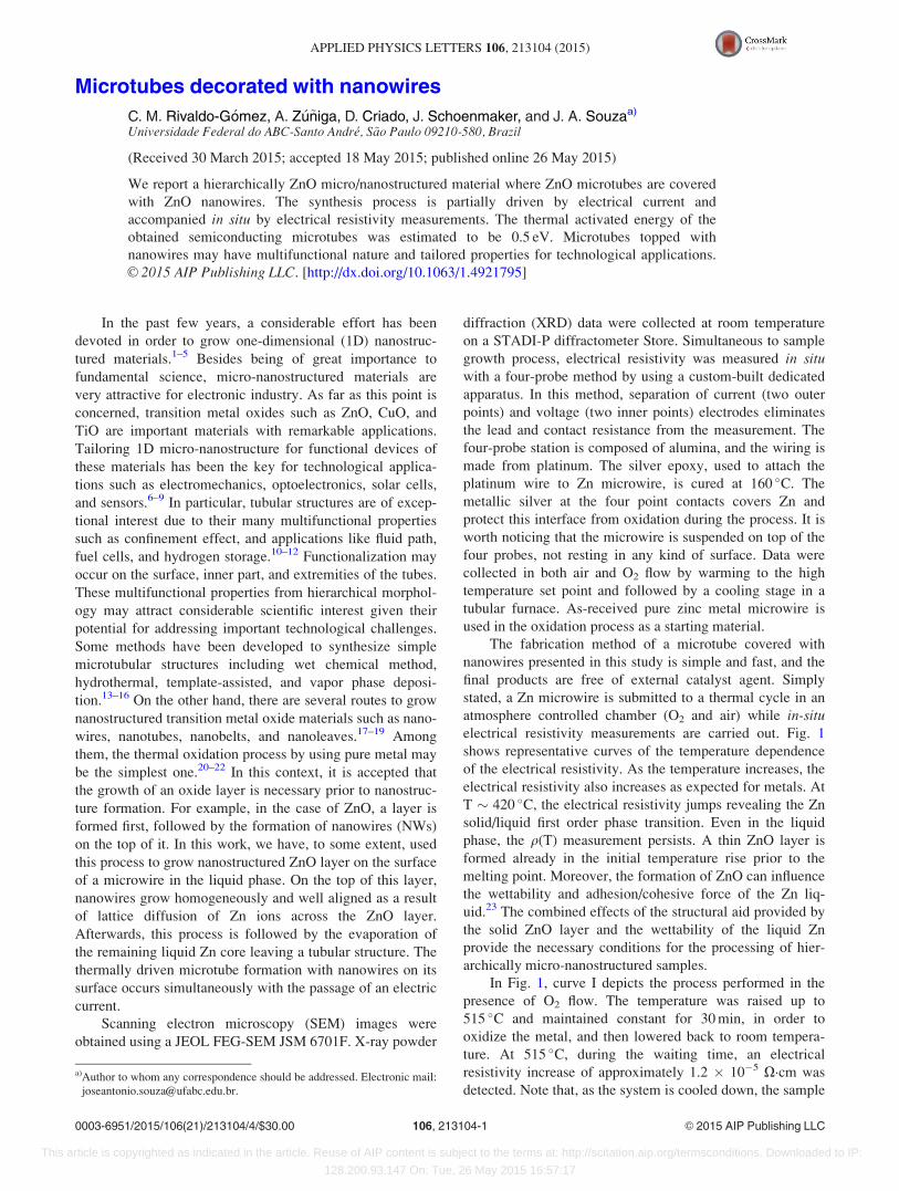
In Fig. 1, curve I depicts the process performed in the
presence of O2 flow. The temperature was raised up to
515 �C and maintained constant for 30 min, in order to
oxidize the metal, and then lowered back to room tempera-
ture. At 515 �C, during the waiting time, an electrical
resistivity increase of approximately 1.2 � 10�5 X�cm was
detected. Note that, as the system is cooled down, the sample
a)Author to whom any correspondence should be addressed. Electronic mail:
0003-6951/2015/106(21)/213104/4/$30.00 VC 2015 AIP Publishing LLC106, 213104-1
APPLIED PHYSICS LETTERS 106, 213104 (2015)
This article is copyrighted as indicated in the article. Reuse of AIP content is subject to the terms at: http://scitation.aip.org/termsconditions. Downloaded to IP:
128.200.93.147 On: Tue, 26 May 2015 16:57:17
undergoes the phase transition from liquid to solid in a
reverse process, however on a slightly higher electrical resis-
tivity level and slightly shifted to a lower temperature. At the
end of the process, the sample is consisted of a metallic core
covered with a nanostructured ZnO shell topped by nanowire
array on the surface. Curve II depicts a measurement similar
to the previously described, except for the 60 min waiting
time. Due to the longer waiting time, the electrical resistivity
jumps suddenly three orders of magnitude. Afterwards, as
the system is cooled down, q increases rather modestly
showing another significant jump around 300 �C. At this
point of the process, the electrical contacts break and the
measurement stops. Other two runs are shown in Fig. 1 and
refer to processes in the presence of O2 flow (curve III) and
in air (curve IV) where the temperature was raised up to
810 �C, followed by cooling the system back to room tem-
perature. The process undertaken in the presence of O2
presents a higher resistivity slope when compared to the pro-
cess in the presence of air flow. At TBDP¼ 680 �C (for O2
flow) and 740 �C (in air), the electrical resistivity increases
sharply suggesting that the metallic percolation path in the
liquid phase brakes down (break down of percolation
(BDP)). In other words, at this temperature, the Zn liquid
medium loses continuity turning into liquid islands through-
out the wire breaking down the path of electrical current. As
time and temperature increase, the metallic islands separated
by ZnO regions become smaller, increasing the electrical
resistivity as revealed by the stair-like behavior of the
curves. The electrical resistivity of ZnO is much higher than
the Zn metal. For the sake of reproducibility, we have
repeated these measurements several times, and the results
are consistent except that the percolation breakdown
temperature is different for each run, however, taking place
in the range from 650 �C to 750 �C. On cooling down from
810 �C, the electrical resistivity increases exponentially
indicating a thermally activated behavior which corroborates
the semiconducting behavior of the produced material (see
Figure 2(b)) (around 600 �C for curve III, the electrical
contacts break and the measurement stops). The electrical
conductivity in semiconductors is described by Arrhenius
equation, q(T)¼q0exp(�EA/kT), where q0 is a constant, EA
the activation energy, k is the Boltzmann constant, and T is
the absolute temperature. In general, at high temperatures
this activation energy is equal to half of the band gap energy
(Eg).24 From the temperature dependence of the electrical re-
sistivity (lnq/q0 versus 1/T), the activation energy is found to
be EA¼ 0.5 eV, which is much lower than the optical energy
gap of the bulk Eg¼ 3.3 eV.25 We suggest that this result,
obtained at very high temperature, is influenced by both the
presence of interstitial Zn species in ZnO lattice and oxygen
vacancies as structural defects.26 As we shall see, in this pro-
cess, one starts with a metal microwire and end up with a
semiconducting microtube decorated with nanowires with
activation energy of 0.5 eV.
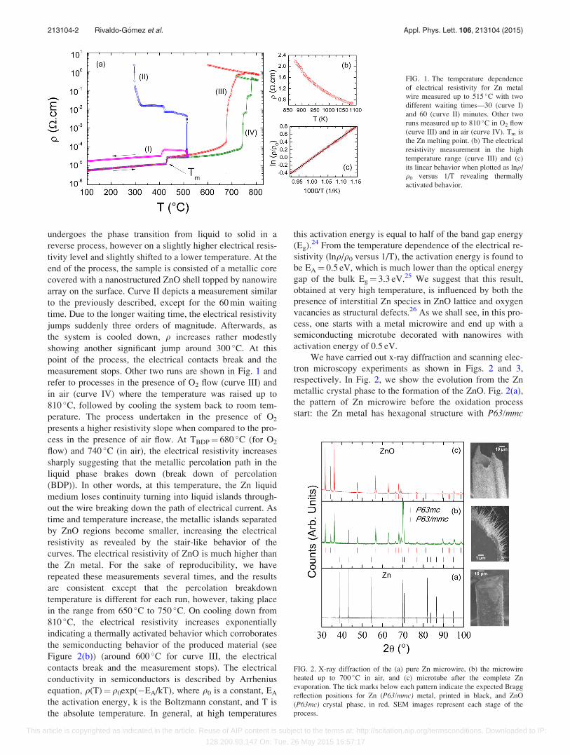
We have carried out x-ray diffraction and scanning elec-
tron microscopy experiments as shown in Figs. 2 and 3,
respectively. In Fig. 2, we show the evolution from the Zn
metallic crystal phase to the formation of the ZnO. Fig. 2(a),
the pattern of Zn microwire before the oxidation process
start: the Zn metal has hexagonal structure with P63/mmc
FIG. 1. The temperature dependence
of electrical resistivity for Zn metal
wire measured up to 515 �C with two
different waiting times—30 (curve I)
and 60 (curve II) minutes. Other two
runs measured up to 810 �C in O2 flow
(curve III) and in air (curve IV). Tm is
the Zn melting point. (b) The electrical
resistivity measurement in the high
temperature range (curve III) and (c)
its linear behavior when plotted as lnq/
q0 versus 1/T revealing thermally
activated behavior.
FIG. 2. X-ray diffraction of the (a) pure Zn microwire, (b) the microwire
heated up to 700 �C in air, and (c) microtube after the complete Zn
evaporation. The tick marks below each pattern indicate the expected Bragg
reflection positions for Zn (P63/mmc) metal, printed in black, and ZnO
(P63mc) crystal phase, in red. SEM images represent each stage of the
process.
213104-2 Rivaldo-G�omez et al. Appl. Phys. Lett. 106, 213104 (2015)
This article is copyrighted as indicated in the article. Reuse of AIP content is subject to the terms at: http://scitation.aip.org/termsconditions. Downloaded to IP:
128.200.93.147 On: Tue, 26 May 2015 16:57:17
space group symmetry. In Fig. 2(b), the x-ray diffraction of a
microwire, heat treated up to 700 �C, in the intermediate pro-
cess is displayed revealing the coexistence of the Zn metallic
and ZnO. In Fig. 3(c), the x-ray diffraction reveals only the
ZnO phase. The ZnO has also a hexagonal structure with
P63mc space group symmetry which is in agreement with lit-
erature. Besides the x-ray diffraction patterns, images show-
ing the morphology of the microwires are accordingly
illustrated.
Figure 3 shows representative images of ZnO micro-
tubes obtained with the process indicated by the curve IV in
Fig. 1. In a first stage, the oxygen present in air reacts with
Zn forming a thin solid layer of ZnO. Note that ZnO melting
point is significantly higher, being Tm¼ 1970 �C. In a second
stage, nanowires are formed as a result of lattice, grain and
surface diffusion of Zn ions from the liquid inner part across
the ZnO layer. During the oxidation process, the ZnO solid
shell covered with nanowires encloses the Zn metallic liquid.
As suggested by the electrical resistivity measurements,
around T¼ 750 �C, the Zn liquid evaporates forming tubular
structures. When the process is carried out in O2 flow atmos-
phere (see curve III in Fig. 1), the oxidation evolution is dif-
ferent. The nanowires grown on the top of ZnO shell have
slightly different morphology—larger diameter and shorter
length. In some cases, the microwire was cut in several seg-
ments after the thermal process with applied electrical cur-
rent. Some sections were tubular and others still presented
the metallic core. In large diameter microwires and depend-
ing on the warming rate, the solid layer does not preserve the
tubular shape of the wire. Instead, the ZnO wall distorts in a
peculiar form with a cross section resembling an 8-shape,
resulting in two attached microtubes. Usually, this problem
can be solved by decreasing the warming temperature rate.
Fig. 3(a) shows an impressive image of the biggest micro-
tube decorated with nanowires, �120 lm in diameter, that
we have obtained, indicating that the metallic Zn core has
completely evaporated even at a temperature much lower
that the Zn boiling point. In this large microtube, the nano-
wires have length from 3 lm to 8 lm and diameter from
200 nm up to 250 nm. Other processes performed in such
wider microwires with higher electrical currents and higher
temperature rates also rendered hollowed structures. In order
to confirm the hollow structure in larger and long micro-
wires, we have broken some of them in a few sections. We
found out that hollowed tubes as long as �300 lm in length
can be processed. Furthermore, one can see in Figs. 3(b) and
3(c) a circular ZnO shell and nanowires growing homogene-
ously up to 10 lm in length and 50 nm in diameter on the top
of it which is in agreement with previous works based on
transmission electron microscopy characterization.27 The
thickness of the oxide layer is around �3 lm.
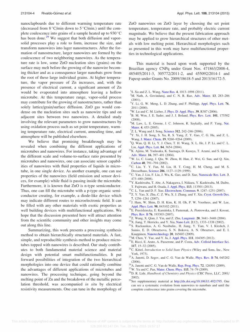
Figure 4 sketches different morphologies assumed by
the microwire as a function of temperature during the pro-
cess. Three main stages may be identified. In the initial stage
(Fig. 4(a)), while the temperature is still bellow the melting
point, a thin ZnO layer is formed on the surface of the micro-
wire. As the temperature rises the ZnO layer thickens and
ZnO nanowires are grown due to lattice diffusion of Zn ions
from the liquid inner part across the layer (Fig. 4(b)). The
formation of the tubular structure is due to the thermal evap-
oration of liquid Zn in high temperature region, however,
below the Zn boiling point. Even though the vapor pressure
of Zn is high,28 we believe that the electric current used to
measure the electrical resistivity plays a role increasing the
evaporation rate of the metallic Zn. The passage of electrical
current may increase the temperature in the inner part of the
microwire (Joule effect) becoming close to the boiling point
of metallic Zn (911 �C) and/or somehow increasing the vapor
pressure of Zn liquid.
We have also observed that the nanowire dimensions
and morphology on the shell can be controlled by the maxi-
mum set point temperature and heating rate—it can be
changed from nanowires to nanobats and nanoclapboards. A
systematic evolution from nanowires to nanobats and to big
FIG. 3. Representative images of SEM showing the formation of nanowires
on the top of microtubes. (a) The biggest obtained microtube decorated with
nanowires with �120 lm in diameter. (b) and (c) Other long microtube with
50 lm in diameter.
FIG. 4. Sketch of the process. (a) Microwire just below the melting point of
Zn (Tm � 420 �C). (b) Core/shell (Zn/ZnO) structure with ZnO nanowires
covering the surface in the liquid phase range. (c) Formation of microtube
after the evaporation of the Zn liquid in the inner part of the wire around
TBDP¼ 700 �C.
213104-3 Rivaldo-G�omez et al. Appl. Phys. Lett. 106, 213104 (2015)
This article is copyrighted as indicated in the article. Reuse of AIP content is subject to the terms at: http://scitation.aip.org/termsconditions. Downloaded to IP:
128.200.93.147 On: Tue, 26 May 2015 16:57:17
nanoclapboards due to different warming temperature rate
(decreased from 8 �C/min down to 5 �C/min.) until the com-
plete coalescence into grains of a sample heated up to 930 �Chas been done.29 We suggest that both diffusion and vapor-
solid processes play a role to form, increase the size, and
transform nanowires into lager nanostructures. After the for-
mation of nanostructure, larger nanowires are formed by the
coalescence of two neighboring nanowires. As the tempera-
ture rate is low, some ZnO nucleation sites (grains) on the
surface may melt before the growing of the nanowire becom-
ing thicker and as a consequence larger nanobats grow from
the root of these large individual grains. At higher tempera-
ture, the vapor pressure of Zn increases, and, with the
presence of electrical current, a significant amount of Zn
would be evaporated into atmosphere leaving a hollow
microtube. At this temperature range, vapor-solid process
may contribute for the growing of nanostructures, rather than
solely lattice/grain/surface diffusion. ZnO gas would con-
dense on the nucleation sites such as nanowire tips and on
adjacent sites between two nanowires. A detailed study
involving the relevant parameters to grow nanostructures by
using oxidation process such as set point temperature, warm-
ing temperature rate, electrical current, annealing time, and
atmosphere will be published elsewhere.
We believe that promising breakthrough may be
revealed when combining the different applications of
microtubes and nanowires. For instance, taking advantage of
the different scale and volume-to-surface ratio presented by
microtubes and nanowires, one can associate sensor capabil-
ities of nanowires with fluid properties of liquids in micro-
tube, in one single device. As another example, one can use
properties of the nanowires (field emission and sensor devi-
ces, for example) while fluid is passing inside the microtube.
Furthermore, it is known that ZnO is n-type semiconductor.
Thus, one can fill the microtube with a p-type organic semi-
conductor creating, for example, a diode-like device which
may indicate different routes to microelectronic field. It can
be filled with any other materials with exotic properties as
well building devices with multifunctional applications. We
hope that the discussion presented here will attract attention
from the scientific community and other insights may come
out along this line.
Summarizing, this work presents a processing synthesis
method to obtain hierarchically structured materials. A fast,
simple, and reproducible synthesis method to produce micro-
tubes topped with nanowires is described. Our study contrib-
utes to both fundamental material science and material
design with potential smart multifunctionalities. It put
forward possibilities of integration of the two hierarchical
morphologies into one device that could rationally combine
the advantages of different applications of microtubes and
nanowires. The processing technique, going beyond the
melting point of Zn and the breakdown of the metallic perco-
lation threshold, was accompanied in situ by electrical
resistivity measurements. One can tune in the morphology of
ZnO nanowires on ZnO layer by choosing the set point
temperature, temperature rate, and probably electric current
magnitude. We believe that the present fabrication approach
may be applied to grow hierarchical structures of other met-
als with low melting point. Hierarchical morphologies such
as presented in this work may have multifunctional proper-
ties in technological applications.
This material is based upon work supported by the
Brazilian agency CNPq under Grant Nos. 471863/2008-4,
485405/2011-3, 305772/2011-2, and 455092/2014-1 and
Fapesp under Grants No. 2009/18618-5 and 2013/16172-5.
1S. Xu and Z. L. Wang, Nano Res. 4, 1013–1098 (2011).2M. Nath, A. Govindaraj, and C. N. R. Rao, Adv. Mater. 13, 283–286
(2001).3Y. Li, G. W. Meng, L. D. Zhang, and F. Phillipp, Appl. Phys. Lett. 76,
2011 (2000).4W. Lu and C. M. Lieber, J. Phys. D: Appl. Phys. 39, R387 (2006).5B. M. Wen, J. E. Sader, and J. J. Boland, Phys. Rev. Lett. 101, 175502
(2008).6M. Law, L. E. Greene, J. C. Johnson, R. Saykally, and P. Yang, Nat.
Mater. 4, 455 (2005).7Z. L. Wang and J. Song, Science 312, 242–246 (2006).8Y. Xi, J. H. Song, S. Xu, R. S. Yang, Z. Y. Gao, C. G. Hu, and Z. L.
Wang, J. Mater. Chem. 19, 9260–9264 (2009).9Q. Wan, Q. H. Li, Y. J. Chen, T. H. Wang, X. L. He, J. P. Li, and C. L.
Lin, Appl. Phys. Lett. 84, 3654 (2004).10K. Ajima, M. Yudasaka, K. Suenaga, D. Kasuya, T. Azami, and S. Iijima,
Adv. Mater. 16, 397–401 (2004).11W. Li, C. Liang, J. Qiu, W. Zhou, H. Han, Z. Wei, G. Sun, and Q. Xin,
Carbon 40, 791–794 (2002).12C. Liu, Y. Y. Fan, M. Liu, H. T. Cong, H. M. Cheng, and M. S.
Dresselhaus, Science 286, 1127–1129 (1999).13C. Yan, J. Liu, F. Liu, J. Wu, K. Gao, and D. Xue, Nanoscale Res. Lett. 3,
473–480 (2008).14Y. Kashiwaba, T. Abe, A. Nakagawa, I. Niikura, Y. Kashiwaba, M. Daibo,
T. Fujiwara, and H. Osada, J. Appl. Phys. 113, 113501 (2013).15C. L. Yan and D. F. Xue, Electrochem. Commun. 9, 1247–1251 (2007).16Z. Y. Yao, X. Zhu, C. Z. Wu, X. J. Zhang, and Y. Xie, Cryst. Growth Des.
7, 1256–1261 (2007).17J. Ham, W. Shim, D. H. Kim, K. H. Oh, P. W. Voorhees, and W. Lee,
Appl. Phys. Lett. 98, 043102 (2011).18E. Prze�zdziecka, E. Kami�nska, I. Pasternak, A. Piotrowska, and J. Kossut,
Phys. Rev. B 76, 193303 (2007).19Z. Wang, X. Qian, J. Yin, and Z. Zhu, Langmuir. 20, 3441–3448 (2004).20X. Jiang, T. Herricks, and Y. Xia, Nano Lett. 2(12), 1333–1338 (2002).21S. Rackauskas, A. G. Nasibulin., H. Jiang, Y. Tian, V. I. Kleshch, J.
Sainio, E. D. Obraztsova, S. N. Bokova, A. N. Obraztsov, and E. I.
Kauppinen, Nanotechnology 20, 165603 (2009).22M. Chen, Y. Yue, and Y. Ju, J. Appl. Phys. 111, 104305 (2012).23E. Ricci, E. Arato, A. Passerone, and P. Costa, Adv. Colloid Interface Sci.
117, 15–32 (2005).24C. Kittel, Introduction to Solid State Physics (Wiley and Sons, Inc., New
York, 1973).25A. Janotti, D. Segev, and C. G. Van de Walle, Phys. Rev. B 74, 045202
(2006).26A. Janotti and C. G. Van de Walle, Rep. Prog. Phys. 72, 126501 (2009).27W. Yu and C. Pan, Mater. Chem. Phys. 115, 74–79 (2009).28D. R. Lide, Handbook of Chemistry and Physics (CRC Press, LLC, 2001/
2002).29See supplementary material at http://dx.doi.org/10.1063/1.4921795. One
can see a systematic evolution from nanowires to nanobats and until the
complete coalescence into grains covering the microtube.
213104-4 Rivaldo-G�omez et al. Appl. Phys. Lett. 106, 213104 (2015)
This article is copyrighted as indicated in the article. Reuse of AIP content is subject to the terms at: http://scitation.aip.org/termsconditions. Downloaded to IP:
128.200.93.147 On: Tue, 26 May 2015 16:57:17