Embed Size (px)
Citation preview
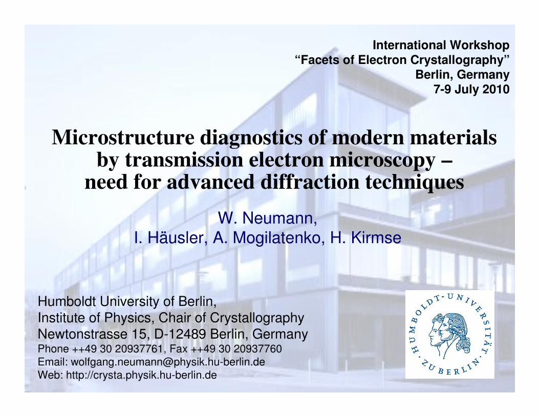
Microstructure diagnostics of modern materials by transmission electron microscopy –
need for advanced diffraction techniques
Humboldt University of Berlin, Institute of Physics, Chair of CrystallographyNewtonstrasse 15, D-12489 Berlin, GermanyPhone ++49 30 20937761, Fax ++49 30 20937760
Email: [email protected]
Web: http://crysta.physik.hu-berlin.de
W. Neumann,
I. Häusler, A. Mogilatenko, H. Kirmse
International Workshop
“Facets of Electron Crystallography”Berlin, Germany
7-9 July 2010
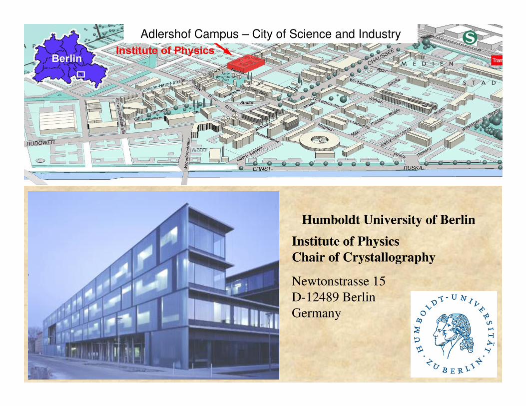
Humboldt University of Berlin
Institute of Physics
Chair of Crystallography
Newtonstrasse 15
D-12489 Berlin
Germany
Adlershof Campus – City of Science and Industry
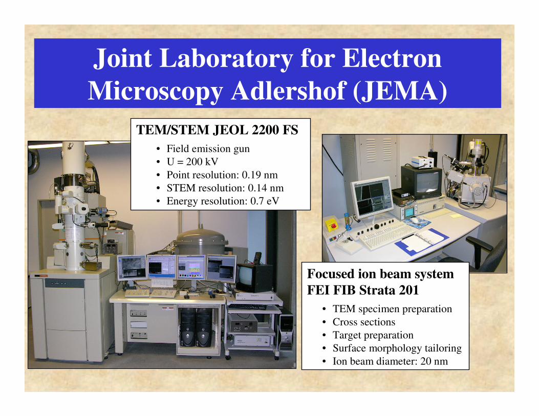
TEM/STEM JEOL 2200 FS
• Field emission gun
• U = 200 kV
• Point resolution: 0.19 nm
• STEM resolution: 0.14 nm
• Energy resolution: 0.7 eV
Focused ion beam system
FEI FIB Strata 201
• TEM specimen preparation
• Cross sections
• Target preparation
• Surface morphology tailoring
• Ion beam diameter: 20 nm
Joint Laboratory for Electron
Microscopy Adlershof (JEMA)
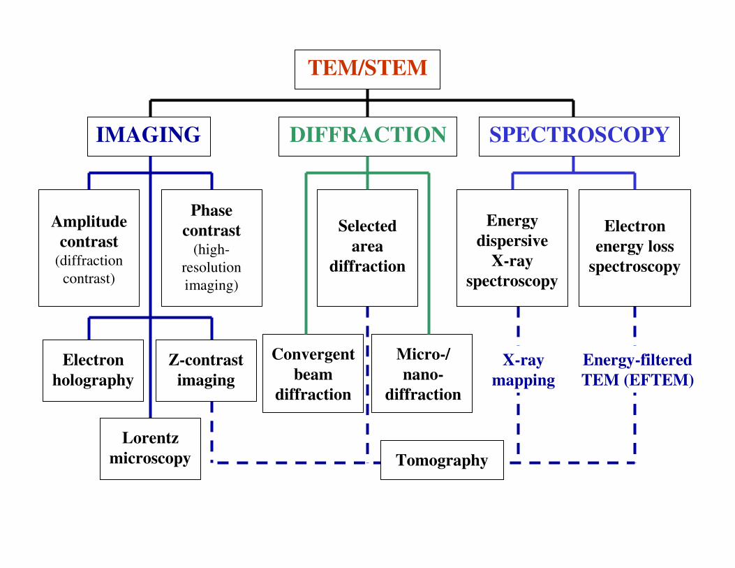
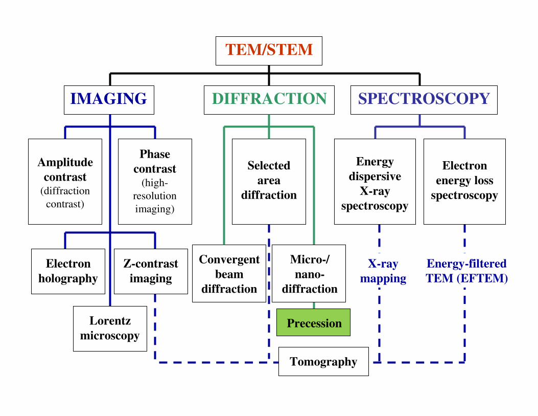
IMAGING DIFFRACTION SPECTROSCOPY
Amplitude
contrast(diffraction
contrast)
Phase
contrast(high-
resolution
imaging)
Selected
area
diffraction
Energy
dispersive
X-ray
spectroscopy
Electron
energy loss
spectroscopy
Electron
holography
Z-contrast
imaging
Convergent
beam
diffraction
Micro-/
nano-
diffraction
Energy-filtered
TEM (EFTEM)
X-ray
mapping
TEM/STEM
Lorentz
microscopy Tomography
IMAGING DIFFRACTION SPECTROSCOPY
Amplitude
contrast(diffraction
contrast)
Phase
contrast(high-
resolution
imaging)
Selected
area
diffraction
Energy
dispersive
X-ray
spectroscopy
Electron
energy loss
spectroscopy
Electron
holography
Z-contrast
imaging
Convergent
beam
diffraction
Energy-filtered
TEM (EFTEM)
X-ray
mapping
TEM/STEM
Lorentz
microscopy
Tomography
Precession
Micro-/
nano-
diffraction
Characterization of
single crystalline LiAlO2 substrates
for subsequent GaN epitaxy
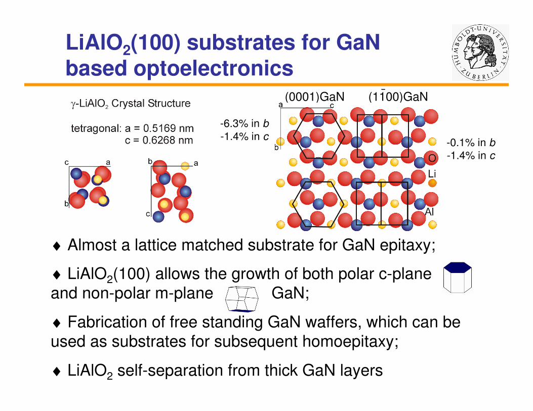
LiAlO2(100) substrates for GaNbased optoelectronics
(0001)GaN (1100)GaN
♦ Almost a lattice matched substrate for GaN epitaxy;
♦ LiAlO2(100) allows the growth of both polar c-plane
and non-polar m-plane GaN;
♦ Fabrication of free standing GaN waffers, which can be
used as substrates for subsequent homoepitaxy;
♦ LiAlO2 self-separation from thick GaN layers
-0.1% in b
-1.4% in c
-6.3% in b
-1.4% in c
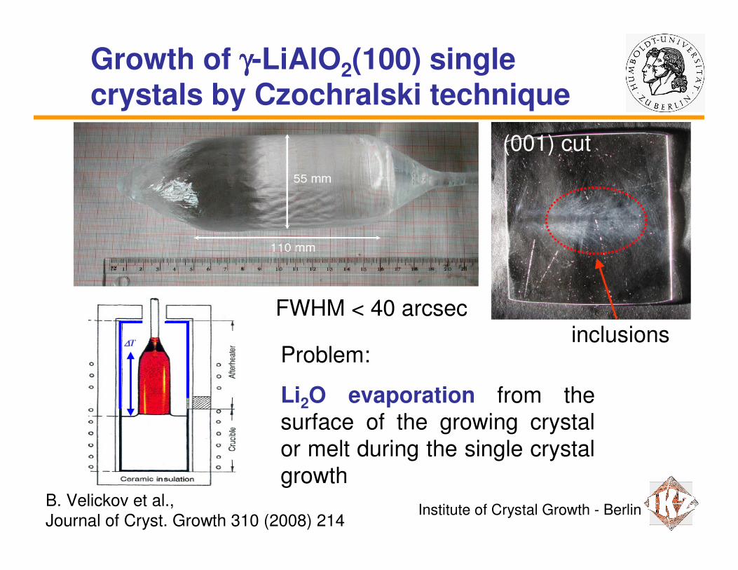
Growth of γγγγ-LiAlO2(100) singlecrystals by Czochralski technique
FWHM < 40 arcsecinclusions
Problem:
Li2O evaporation from thesurface of the growing crystal
or melt during the single crystal
growth
Institute of Crystal Growth - BerlinB. Velickov et al.,
Journal of Cryst. Growth 310 (2008) 214
(001) cut
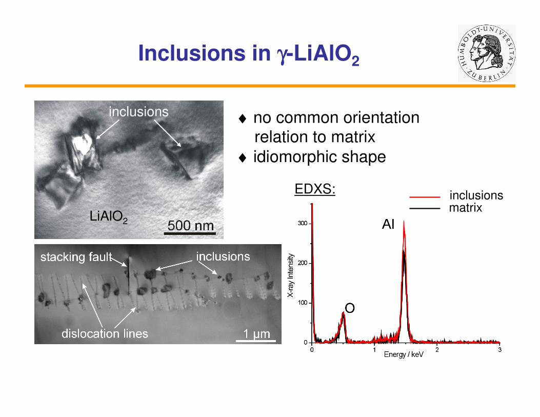
Inclusions in γγγγ-LiAlO2
♦ no common orientationrelation to matrix
♦ idiomorphic shape
LiAlO2
inclusions
EDXS: inclusionsmatrix
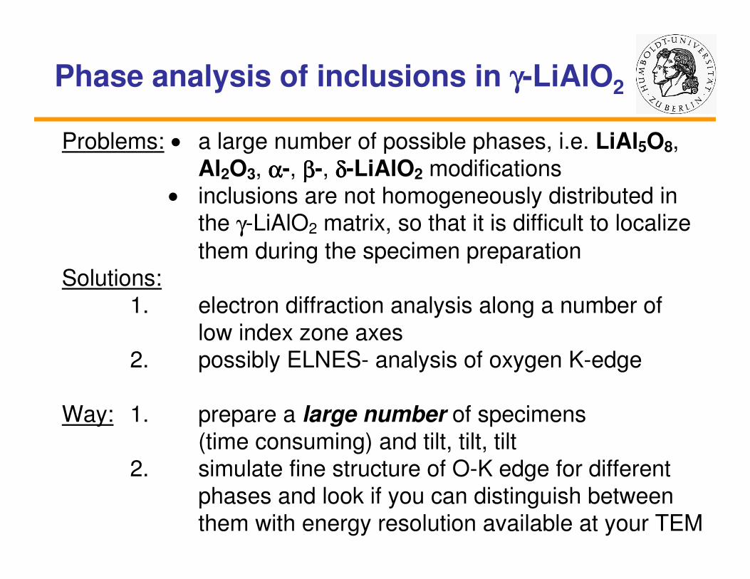
Phase analysis of inclusions in γγγγ-LiAlO2
Problems: • a large number of possible phases, i.e. LiAl5O8,
Al2O3, αααα-, ββββ-, δδδδ-LiAlO2 modifications
• inclusions are not homogeneously distributed inthe γ-LiAlO2 matrix, so that it is difficult to localize
them during the specimen preparationSolutions:
1. electron diffraction analysis along a number of
low index zone axes2. possibly ELNES- analysis of oxygen K-edge
Way: 1. prepare a large number of specimens
(time consuming) and tilt, tilt, tilt2. simulate fine structure of O-K edge for different
phases and look if you can distinguish between
them with energy resolution available at your TEM
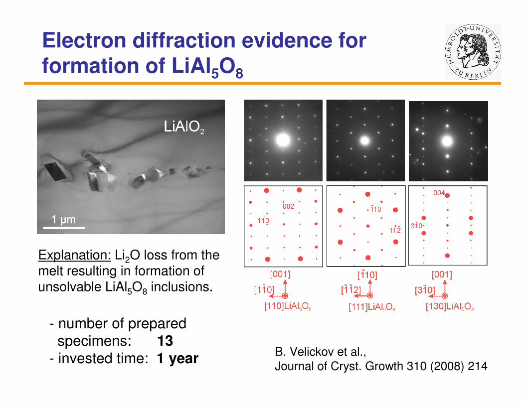
Electron diffraction evidence for formation of LiAl5O8
Explanation: Li2O loss from themelt resulting in formation of unsolvable LiAl5O8 inclusions.
B. Velickov et al.,
Journal of Cryst. Growth 310 (2008) 214
- number of prepared
specimens: 13- invested time: 1 year
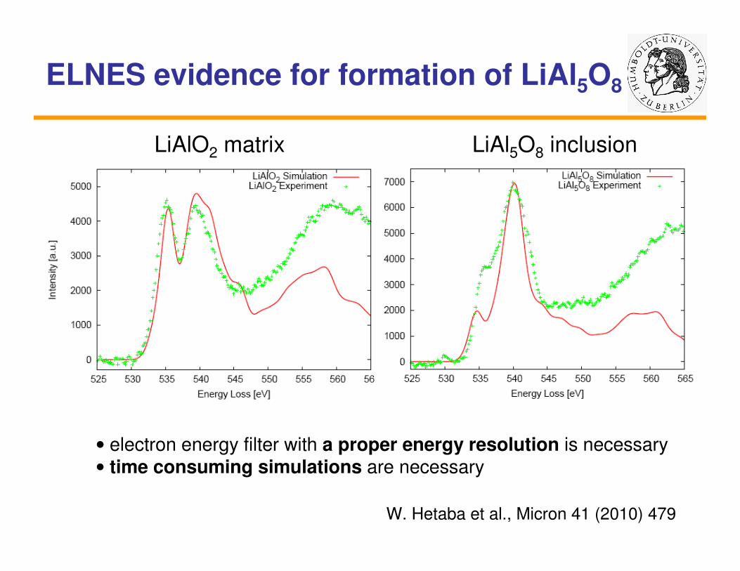
ELNES evidence for formation of LiAl5O8
• electron energy filter with a proper energy resolution is necessary• time consuming simulations are necessary
LiAlO2 matrix LiAl5O8 inclusion
W. Hetaba et al., Micron 41 (2010) 479
FePt crystallites on
self-assembled SiO2 nanospheres
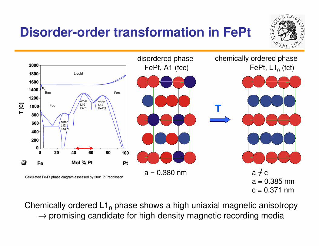
Disorder-order transformation in FePt
a = 0.380 nm
FePt, A1 (fcc)
a = c
a = 0.385 nm
c = 0.371 nm
FePt, L10 (fct)
chemically ordered phasedisordered phase
Chemically ordered L10 phase shows a high uniaxial magnetic anisotropy
→ promising candidate for high-density magnetic recording media
T
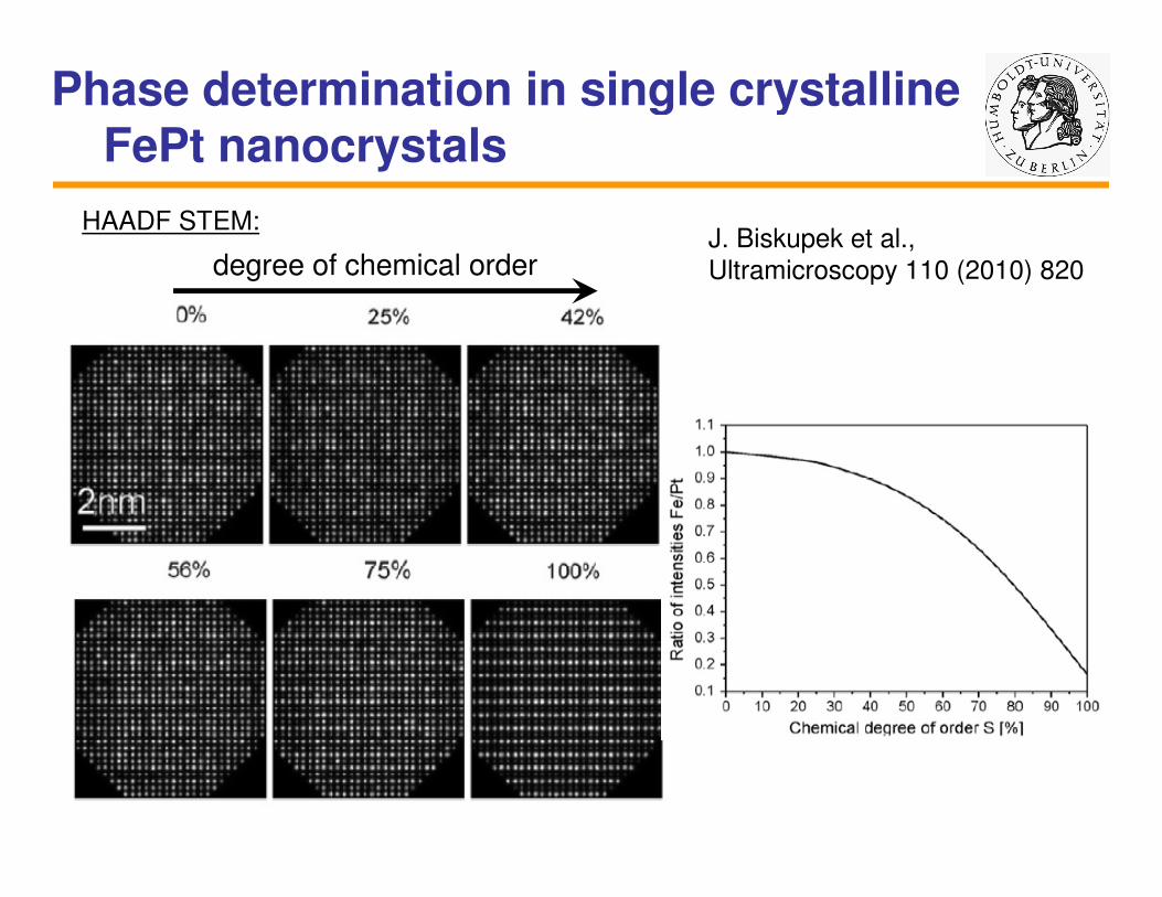
Phase determination in single crystallineFePt nanocrystals
degree of chemical orderJ. Biskupek et al.,
Ultramicroscopy 110 (2010) 820
HAADF STEM:
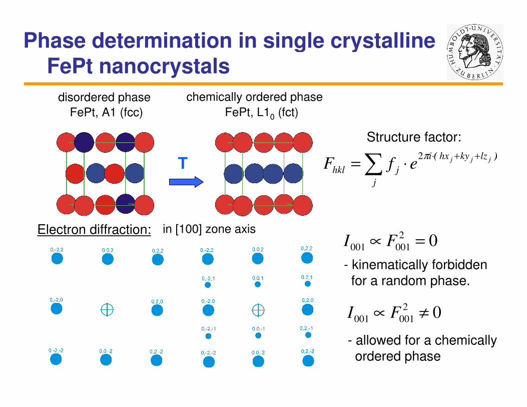
Phase determination in single crystallineFePt nanocrystals
FePt, A1 (fcc) FePt, L10 (fct)
chemically ordered phasedisordered phase
T
Electron diffraction: in [100] zone axis
∑++⋅
⋅=j
lzkyhxi
jhkl
jjjefF)(π2
02
001001 =∝ FI
- kinematically forbidden for a random phase.
02
001001 ≠∝ FI
- allowed for a chemically ordered phase
Structure factor:
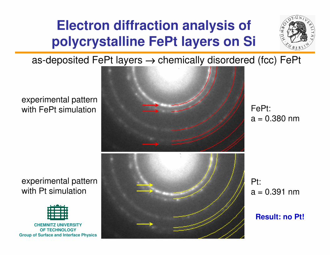
as-deposited FePt layers →→→→ chemically disordered (fcc) FePt
experimental patternwith FePt simulation
Result: no Pt!
Electron diffraction analysis of polycrystalline FePt layers on Si
experimental patternwith Pt simulation
FePt:a = 0.380 nm
Pt:a = 0.391 nm
CHEMNITZ UNIVERSITY
OF TECHNOLOGY
Group of Surface and Interface Physics
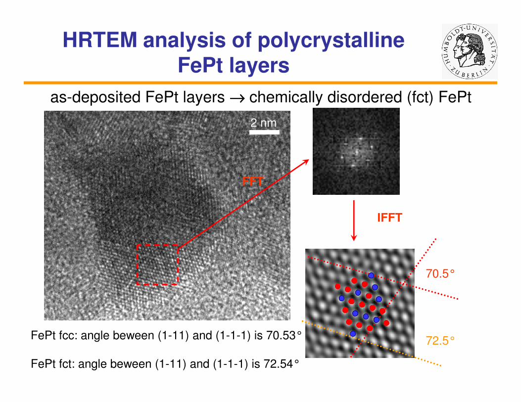
2 nm
FFT
IFFT
70.5°
FePt fcc: angle beween (1-11) and (1-1-1) is 70.53°
FePt fct: angle beween (1-11) and (1-1-1) is 72.54°
72.5°
as-deposited FePt layers →→→→ chemically disordered (fct) FePt
HRTEM analysis of polycrystalline FePt layers
2 nm
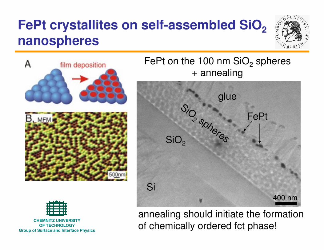
FePt crystallites on self-assembled SiO2
nanospheres
FePt on the 100 nm SiO2 spheres
+ annealing
annealing should initiate the formation
of chemically ordered fct phase!
Si
SiO2
glue
FePtSiO
2 spheres
400 nm
CHEMNITZ UNIVERSITY
OF TECHNOLOGY
Group of Surface and Interface Physics
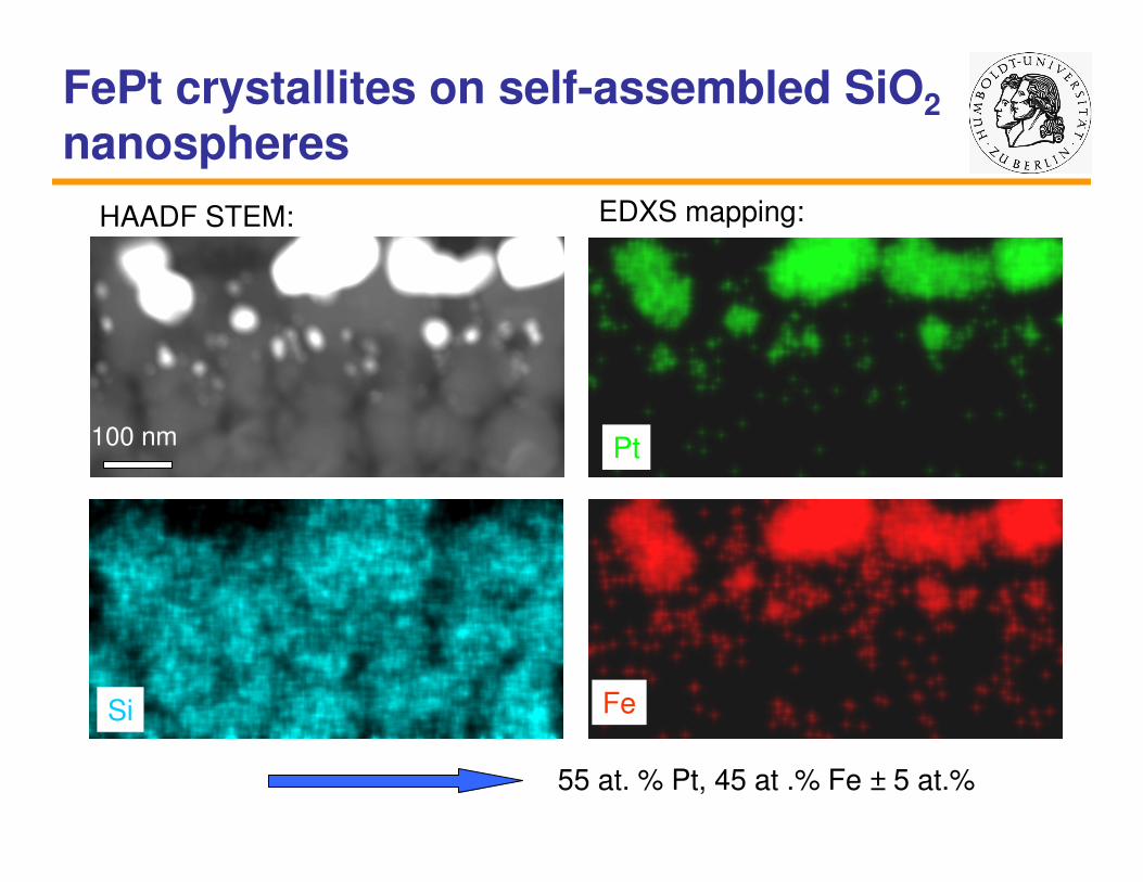
FePt crystallites on self-assembled SiO2
nanospheres
100 nm
HAADF STEM:
Pt
Fe
EDXS mapping:
Si
55 at. % Pt, 45 at .% Fe ± 5 at.%
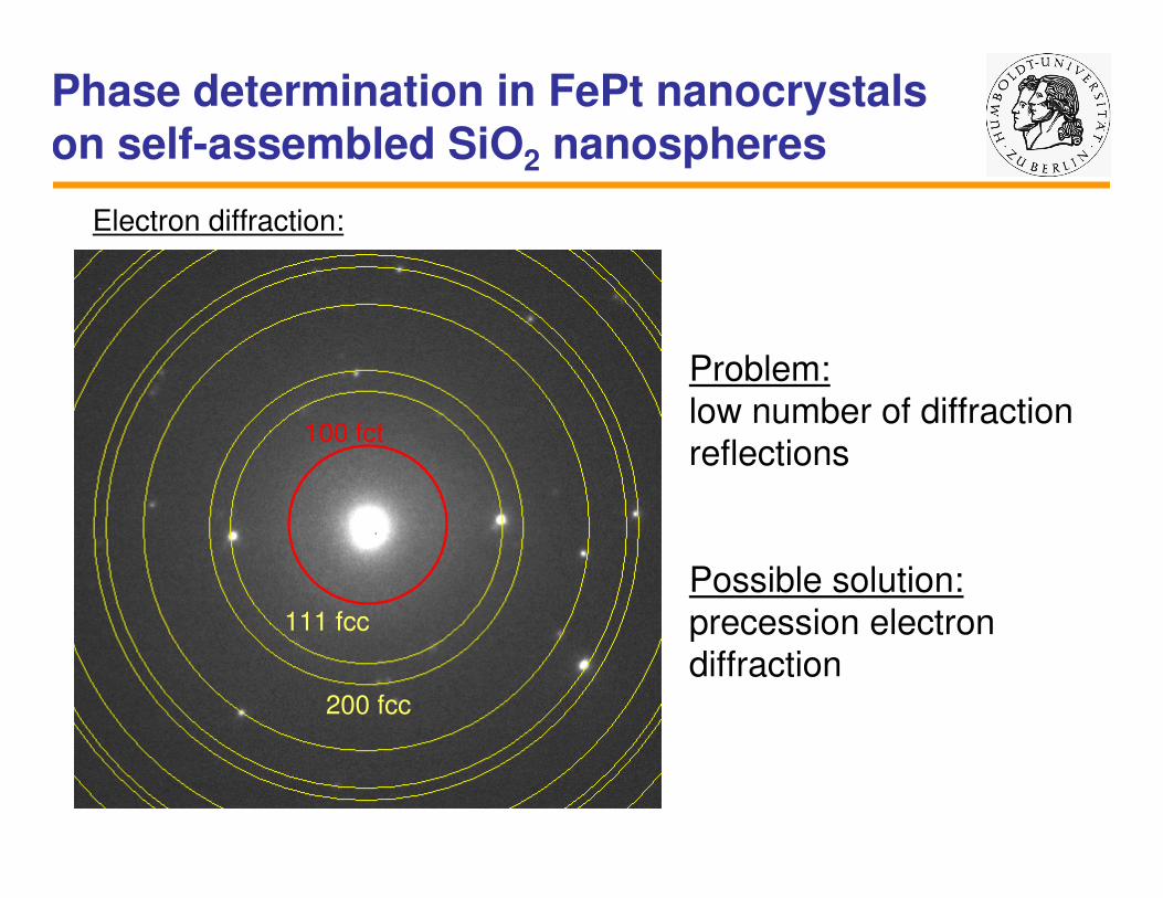
Phase determination in FePt nanocrystals
on self-assembled SiO2 nanospheres
Electron diffraction:
Problem:
low number of diffractionreflections
Possible solution:
precession electrondiffraction
111 fcc
200 fcc
100 fct
Crystallite phase and orientation
mapping of MnAs in GaAs
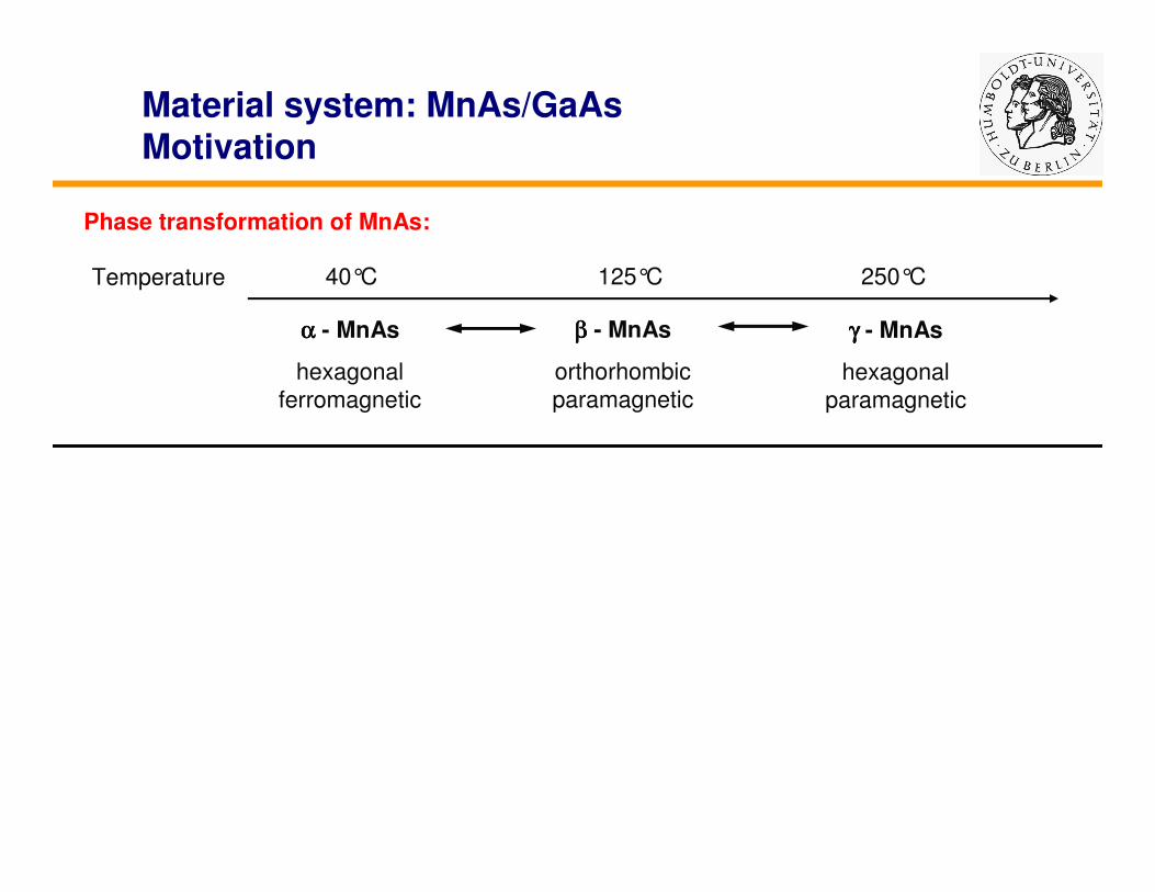
αααα - MnAs
hexagonal
ferromagnetic
ββββ - MnAs
orthorhombic
paramagnetic
γγγγ - MnAs
hexagonal
paramagnetic
Temperature 40°C 125°C 250°C
Phase transformation of MnAs:
Material system: MnAs/GaAsMotivation
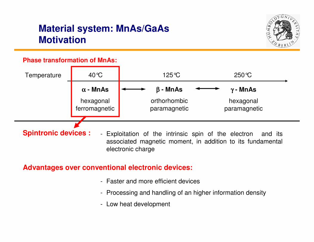
αααα - MnAs
hexagonal
ferromagnetic
ββββ - MnAs
orthorhombic
paramagnetic
γγγγ - MnAs
hexagonal
paramagnetic
Temperature 40°C 125°C 250°C
Material system: MnAs/GaAsMotivation
Spintronic devices : - Exploitation of the intrinsic spin of the electron and its
associated magnetic moment, in addition to its fundamental
electronic charge
Advantages over conventional electronic devices:
- Faster and more efficient devices
- Processing and handling of an higher information density
- Low heat development
Phase transformation of MnAs:
Growth of MnAs/GaAs
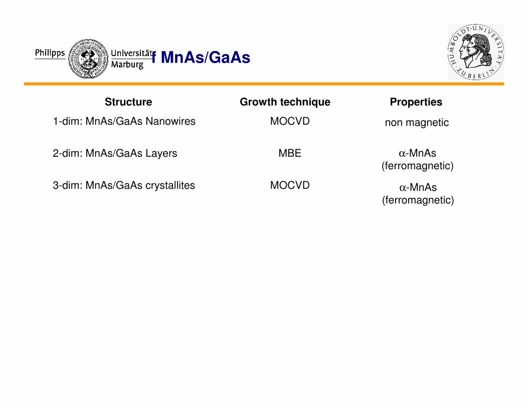
1-dim: MnAs/GaAs Nanowires
2-dim: MnAs/GaAs Layers
3-dim: MnAs/GaAs crystallites
MOCVD
MBE
MOCVD
Structure Growth technique Properties
α-MnAs(ferromagnetic)
α-MnAs(ferromagnetic)
non magnetic
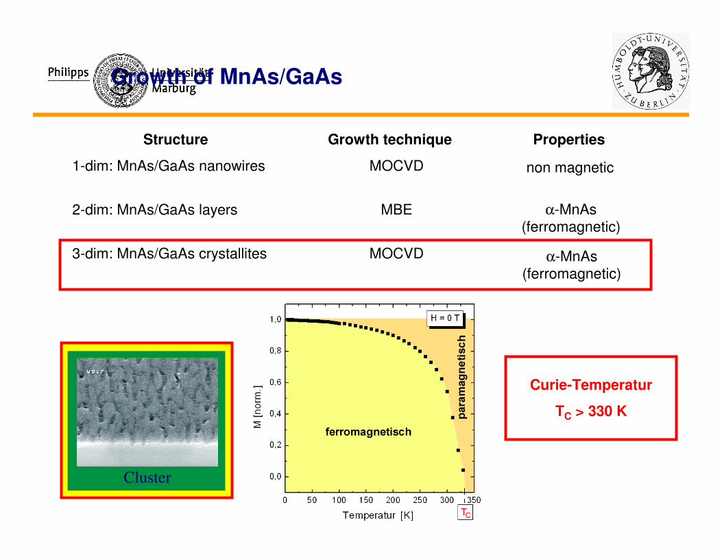
Growth of MnAs/GaAs
1-dim: MnAs/GaAs nanowires
2-dim: MnAs/GaAs layers
3-dim: MnAs/GaAs crystallites
MOCVD
MBE
MOCVD
Structure Growth technique Properties
α-MnAs(ferromagnetic)
α-MnAs(ferromagnetic)
non magnetic
Curie-Temperatur
TC > 330 K
Cluster
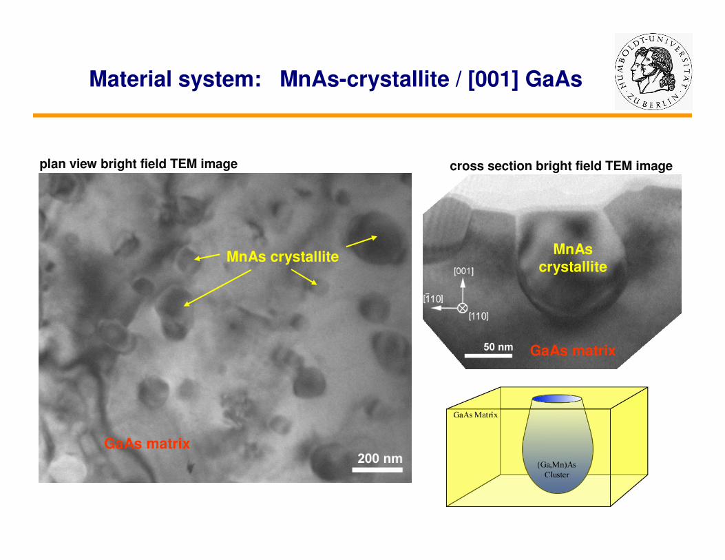
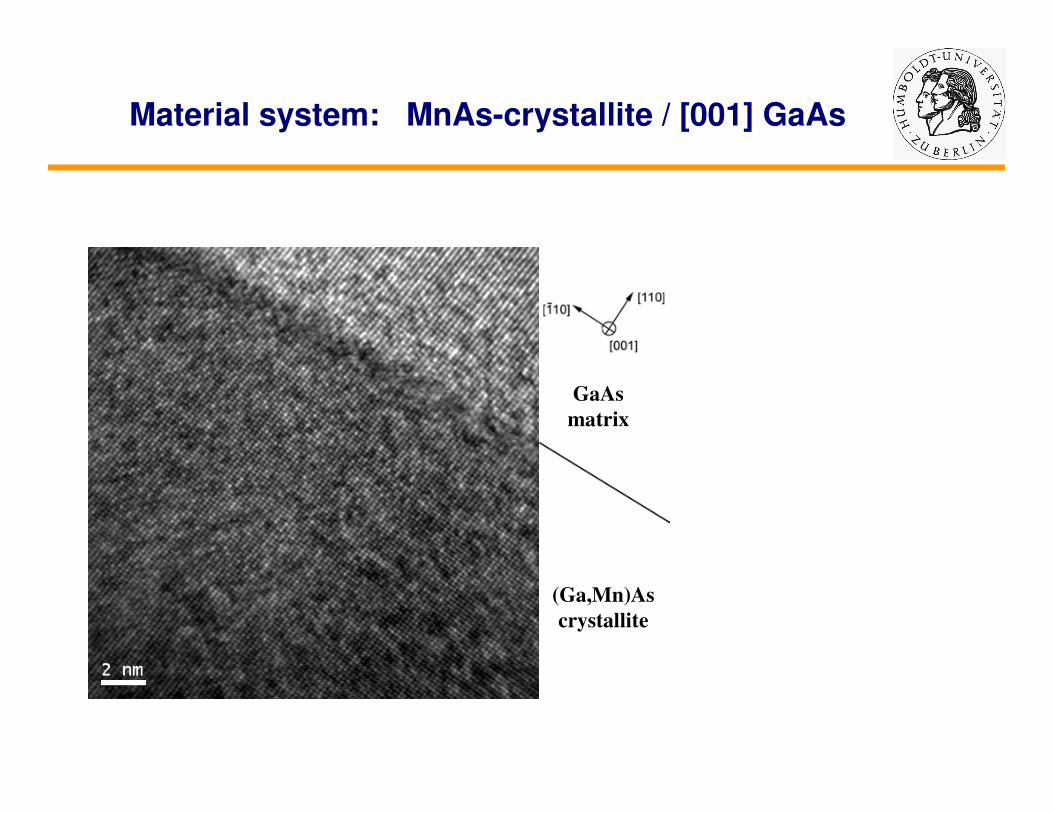
Material system: MnAs-crystallite / [001] GaAs
plan view bright field TEM image cross section bright field TEM image
MnAs crystalliteMnAs
crystallite
GaAs matrix
GaAs matrix
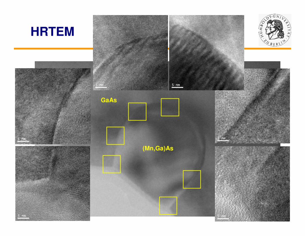
HRTEM
(Mn,Ga)As
GaAs
Material system: MnAs-crystallite / [001] GaAs
(Ga,Mn)As
crystallite
GaAs
matrix
FFT
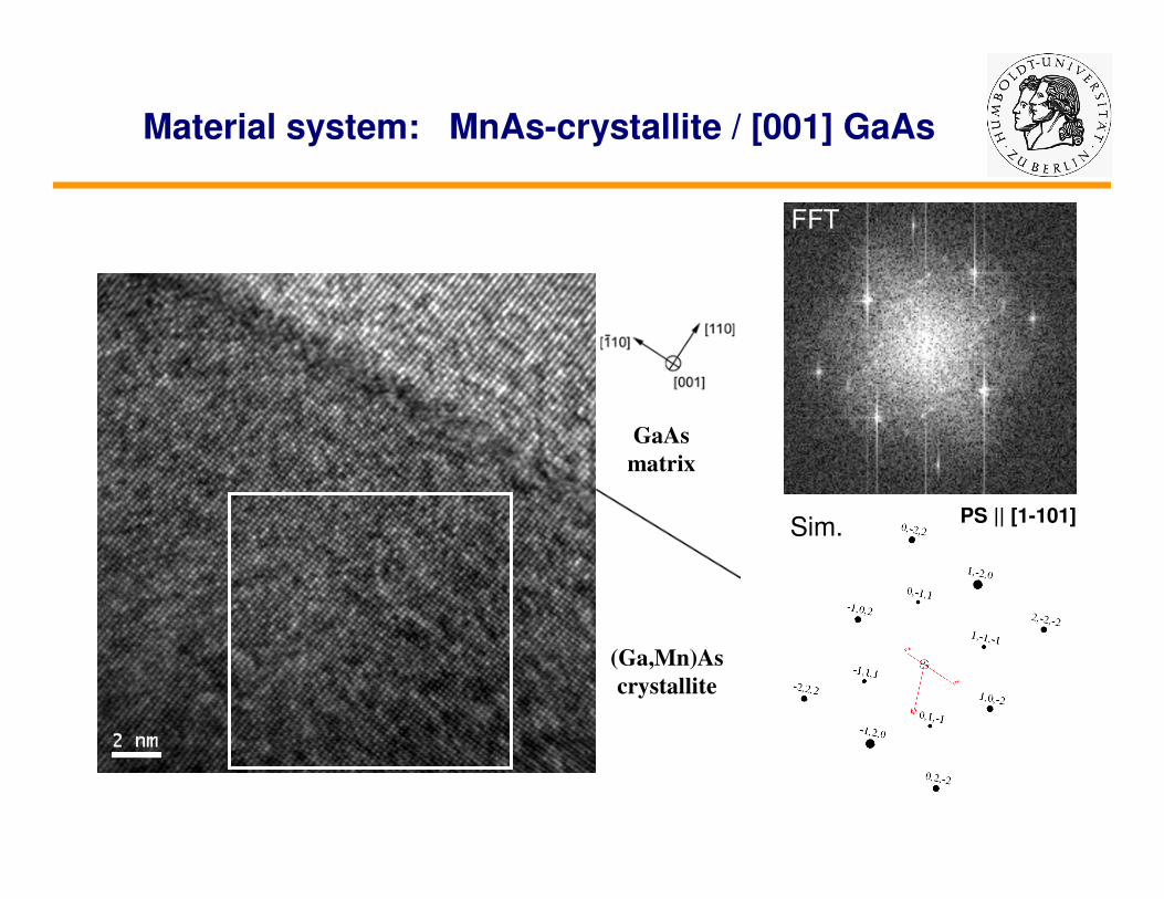
Material system: MnAs-crystallite / [001] GaAs
(Ga,Mn)As
crystallite
GaAs
matrix
FFT
PS || [1-101]Sim.
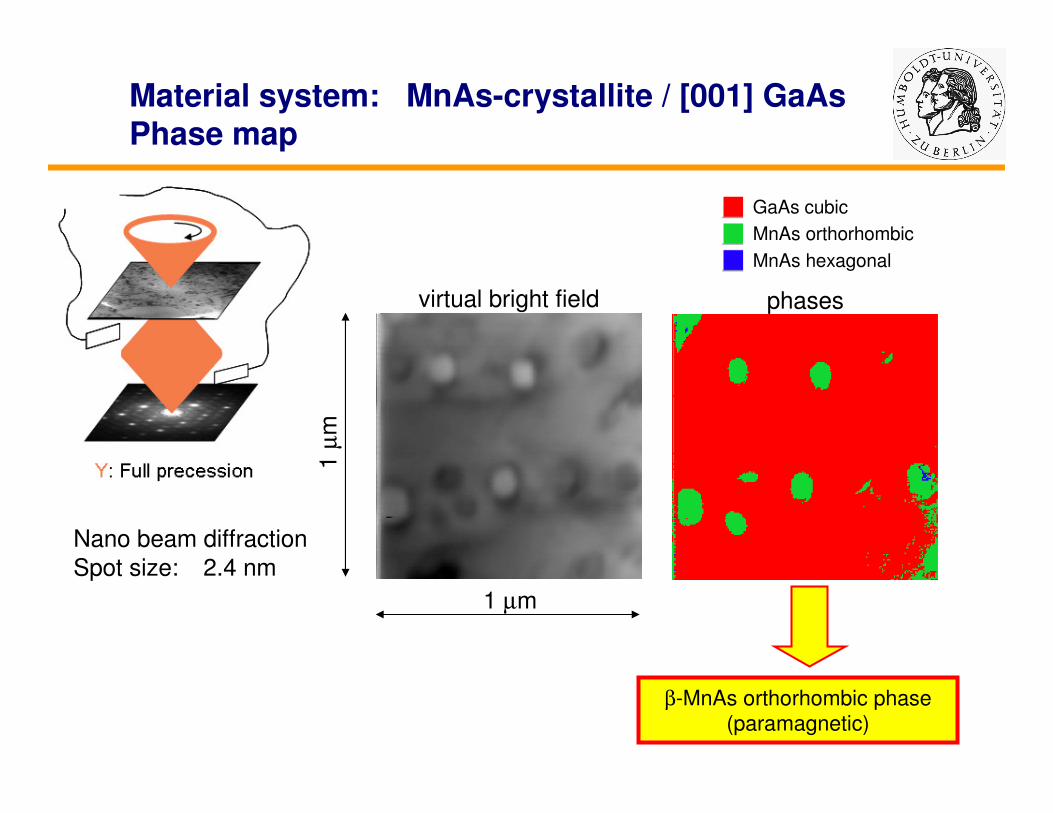
Material system: MnAs-crystallite / [001] GaAsPhase map
phasesvirtual bright field
1 µ
m
1 µm
β-MnAs orthorhombic phase(paramagnetic)
Nano beam diffraction
Spot size: 2.4 nm
GaAs cubic
MnAs orthorhombic
MnAs hexagonal
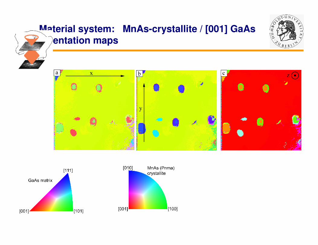
Material system: MnAs-crystallite / [001] GaAsOrientation maps
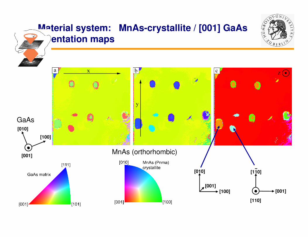
Material system: MnAs-crystallite / [001] GaAsOrientation maps
[001]
[100]
[010]
GaAs
[001]
[010]
[100]
MnAs (orthorhombic)
[110]
[001]
[110]
Scientific contributions of
Anna Mogilatenko Holm Kirmse Ines Häusler

Thank you for your attention