Embed Size (px)
Citation preview

MICROSTRIP POST PRODUCTION TUNING BAR ERROR AND
COMPACT RESONATORS USING NEGATIVE REFRACTIVE
INDEX METAMATERIALS
A Thesis
by
AARON DAVID SCHER
Submitted to the Office of Graduate Studies of
Texas A&M University in partial fulfillment of the requirements for the degree of
MASTER OF SCIENCE
May 2005
Major Subject: Electrical Engineering

MICROSTRIP POST PRODUCTION TUNING BAR ERROR AND
COMPACT RESONATORS USING NEGATIVE REFRACTIVE
INDEX METAMATERIALS
A Thesis
by
AARON DAVID SCHER
Submitted to the Office of Graduate Studies of
Texas A&M University in partial fulfillment of the requirements for the degree of
MASTER OF SCIENCE
Approved as to style and content by: _____________________________ _____________________________ Kai Chang Krzysztof Michalski (Chair of Committee) (Member) _____________________________ _____________________________ Henry Taylor Wayne Saslow (Member) (Member)
_____________________________ Chanan Singh
(Head of Department)
May 2005
Major Subject: Electrical Engineering

iii
ABSTRACT
Microstrip Post Production Tuning Bar Error and Compact Resonators
Using Negative Refractive Index Metamaterials. (May 2005)
Aaron David Scher, B.S., Texas A&M University
Chair of Advisory Committee: Dr. Kai Chang
In this thesis, two separate research topics are undertaken both in the general area
of compact RF/microwave circuit design. The first topic involves characterizing the
parasitic effects and error due to unused post-production tuning bars. Such tuning bars
are used in microwave circuit designs to allow the impedance or length of a microstrip
line to be adjusted after fabrication. In general, the tuning bars are simply patterns of
small, isolated sections of conductor adjacent to the thru line. Changing the impedance
or length of the thru line involves bonding the appropriate tuning bars to the line.
Unneeded tuning bars are simply not removed and left isolated. Ideally, there should be
no coupling between these unused tuning bars and the thru line. Therefore, the unused
tuning bars should have a negligible effect on the circuit’s overall performance. To
nullify the parasitic effects of the tuning bars, conventional wisdom suggests placing the
bars 1.0 to 1.5 substrate heights away from the main line. While successful in the past,
this practice may not result in the most efficient and cost-effective placement of tuning
bars in today’s compact microwave circuits. This thesis facilitates the design of compact
tuning bar configurations with minimum parasitic effects by analyzing the error
attributable to various common tuning bar configurations with a range of parameters and
offset distances. The error is primarily determined through electromagnetic simulations,
and the accuracy of these simulations is verified by experimental results. The second
topic in this thesis involves the design of compact microwave resonators using the
transmission line approach to create negative refractive index metamaterials. A survey
of the major developments and fundamental concepts related to negative refractive index
technology (with focus on the transmission line approach) is given. Following is the

iv
design and measurement of the compact resonators. The resonators are also compared to
their conventional counterparts to demonstrate both compactness and harmonic
suppression.

v
In Memory of
Marian Scher
1953-1986

vi
ACKNOWLEDGEMENTS
I wish to thank Dr. Chang for his continuous help and guidance throughout my
work on my masters degree. I would also like to thank Dr. Michalski, Dr. Taylor, and
Dr. Saslow for serving as members on my thesis committee. I also thank Mr. Li for his
fabrication and technical assistance. Next, I would like to thank Raytheon Co.,
Electronic Systems Division for their support of this research. The constant
encouragement and suggestions of S.P. McFarlane and J.L. Klein are acknowledged.
Finally, I wish to express my deep appreciation to my family for all their love and
support.

vii
TABLE OF CONTENTS
Page
ABSTRACT ......................................................................................................... iii DEDICATION....................................................................................................... v ACKNOWLEDGEMENTS .................................................................................. vi TABLE OF CONTENTS ..................................................................................... vii LIST OF TABLES ................................................................................................ ix LIST OF FIGURES .............................................................................................. x CHAPTER I INTRODUCTION..................................................................................... 1 II POST PRODUCTION TUNING BAR ERROR IN MICROWAVE CIRCUITS................................................................................................. 3 A. Introduction ................................................................................. 3 1. Statement of Work ............................................................... 3 2. Objectives............................................................................ 3 3. Simulation and CAD Software............................................ 4 4. Research Methods and Approach........................................ 4 5. Summary ............................................................................. 5 B. GaAs MMIC Tuning Bar Configuration ..................................... 5 1. Matched Load...................................................................... 8 2. Mismatched Load................................................................ 10 3. Resonant Frequency Error Analysis .................................... 15 4. Equivalent Circuit ............................................................... 17 5. U-Shaped Tuning Bars ........................................................ 20 6. Conclusions ......................................................................... 24 C. Thin Film Network Tuning Bar Configurations .......................... 24 1. Line-Lengthening Tuning Stub Configuration .................... 25 2. 6×16 mil² Rectangular Tuning Chips in a Cluster (RTCC).. 30 3. 10×10 mil² RTCC................................................................. 39 4. Mismatched Lines with High VSWR.................................. 47 5. Conclusions ......................................................................... 47

viii
CHAPTER Page D. Measurements and Experimental Validation ............................... 48 1. Circuit Layout ..................................................................... 48 2. Measurements...................................................................... 49 3. Conclusions ......................................................................... 52 E. Recommendations and Conclusions ........................................... 52 1. Summary ............................................................................. 52 2. Recommendations ............................................................... 54 III COMPACT RESONATORS USING THE TRANSMISSION LINE APPROACH OF NEGATIVE REFRACTIVE INDEX METAMATERIALS ................................................................................. 58 A. Introduction ................................................................................. 58 B. The Transmission Line Approach to NRI Metamaterials ............ 61 C. Compact Zeroth-Order Resonators Using NRI Microstrip Line . 67 1. Line Resonators................................................................... 68 2. Ring Resonators .................................................................. 71 C. Conclusions ................................................................................. 74 IV SUMMARY AND RECOMMENDATIONS FOR FUTURE STUDY .... 75 A. Summary ..................................................................................... 75 B. Recommendations for Future Study ............................................ 76 REFERENCES..................................................................................................... 77 APPENDIX A MATLAB CODE FOR GENERATING NRI TL DISPERSION DIAGRAM................................................................................. 81 VITA ................................................................................................................... 84

ix
LIST OF TABLES TABLE Page 1 Simulated GaAs tuning bar error results for three important cases. Errors are for matched load (VSWR=1). .................................................. 9 2 Simulated GaAs quarter wave stub resonant frequency error results for
three important cases. ................................................................................ 17
3 Simulated line-lengthening tuning stub error results for three important cases.... ...................................................................................................... 27
4 Simulated TFN quarter wave stub resonant frequency error results for
three important cases. ................................................................................ 30 5 Recommended GaAs MMIC tuning bar offset distances.......................... 55 6 Recommended TFN line-lengthening tuning stub offset distances........... 56 7 Recommended TFN rectangular tuning chip configuration offset
distances. ................................................................................................... 57

x
LIST OF FIGURES
FIGURE Page
1 (a) Top and (b) side view of rectangular GaAs MMIC tuning bar configuration ............................................................................................. 6
2 Simulated GaAs MMIC (a) rectangular tuning bar configuration and
(b) reference thru line ................................................................................ 7 3 ADS optimization screenshot.................................................................... 11
4 Maximum (a) Zin, (b) |S21 magnitude|, and (c) |S21 phase| error factors. Z0 = 50 Ω, L = 200 um, substrate thickness = 100 um, and VSWR = 2.... 12
5 Maximum (a) Zin, (b) |S21 magnitude|, and (c) |S21 phase| error factors. Z0=25 Ω, L = 200 um, substrate thickness = 100 um, and VSWR = 2. .... 13
6 Maximum Zin error factors for (a) L = 100 um and (b) L = 150 um.
Substrate thickness = 100 um, Z0 = 50 Ω, and VSWR = 2........................ 14 7 Maximum Zin error factor for (a) L = 100 um and (b) L = 150 um.
Substrate thickness = 100 um, Z0 = 25 Ω, and VSWR = 2........................ 15 8 GaAs MMIC quarter wave stub resonant circuit at (a) 10 GHz and (b) 35 GHz with rectangular tuning bar. ................................................... 16 9 Tuning bar configuration. (a) coupled line section representation and (b) equivalent circuit ....................................................................................... 19 10 GaAs MMIC U-shaped tuning bar configuration. .................................... 21 11 Maximum (a) Zin, (b) |S21 magnitude|, and (c) |S21 phase| error factors for U-shaped tuning bar. Z0 = 50 Ω, substrate thickness = 100 um, Lpath = 267 um, and VSWR = 2. ................................................................ 22 12 Maximum (a) Zin, (b) |S21 magnitude|, and (c) |S21 phase| error factors
for U-shaped tuning bar. Z0 = 25 Ω, substrate thickness = 100 um, Lpath = 560 um, and VSWR = 2. ................................................................ 23
13 Typical TFN line-lengthening tuning stub geometry ................................ 25
xi
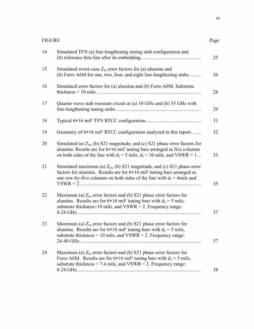
FIGURE Page 14 Simulated TFN (a) line-lengthening tuning stub configuration and
(b) reference thru line after de-embedding................................................ 25 15 Simulated worst-case Zin error factors for (a) alumina and (b) Ferro A6M for one, two, four, and eight line-lengthening stubs. ........ 26 16 Simulated error factors for (a) alumina and (b) Ferro A6M. Substrate thickness = 10 mils. ................................................................................... 28 17 Quarter wave stub resonant circuit at (a) 10 GHz and (b) 35 GHz with line-lengthening tuning stubs .................................................................... 29 18 Typical 6×16 mil² TFN RTCC configuration. ........................................... 31 19 Geometry of 6×16 mil² RTCC configuration analyzed in this report. ...... 32 20 Simulated (a) Zin, (b) S21 magnitude, and (c) S21 phase error factors for alumina. Results are for 6×16 mil² tuning bars arranged in five columns on both sides of the line with d1 = 5 mils, d2 = 10 mils, and VSWR = 1... 33 21 Simulated maximum (a) Zin, (b) S21 magnitude, and (c) S21 phase error factors for alumina. Results are for 6×16 mil² tuning bars arranged as one row-by-five columns on both sides of the line with d1 = 4mils and VSWR = 2. ................................................................................................ 35 22 Maximum (a) Zin error factors and (b) S21 phase error factors for alumina. Results are for 6×16 mil² tuning bars with d2 = 5 mils, substrate thickness=10 mils, and VSWR = 2. Frequency range: 8-24 GHz. .................................................................................................. 37 23 Maximum (a) Zin error factors and (b) S21 phase error factors for alumina. Results are for 6×16 mil² tuning bars with d2 = 5 mils, substrate thickness = 10 mils, and VSWR = 2. Frequency range: 24-40 GHz. ................................................................................................ 37 24 Maximum (a) Zin error factors and (b) S21 phase error factors for Ferro A6M. Results are for 6×16 mil² tuning bars with d2 = 5 mils, substrate thickness = 7.4 mils, and VSWR = 2. Frequency range: 8-24 GHz. .................................................................................................. 38

xii
FIGURE Page 25 Maximum (a) Zin error factors and (b) S21 phase error factors for Ferro A6M. Results are for 6×16 mil² tuning bars with d2 = 5 mils, substrate thickness = 7.4 mils, and VSWR = 2. Frequency range: 24-40 GHz. ................................................................................................ 38 26 Typical 10×10 mil² TFN RTCC. ............................................................... 39 27 Simulated (a) Zin, (b) S21 magnitude, and (c) S21 phase error factors for alumina. Results are for 10×10 mil² tuning bars arranged in five columns on both sides of the line with d1 = 5 mils, d2 = 10 mils, and VSWR=1..... 41 28 Simulated maximum (a) Zin, (b) S21 magnitude, and (c) S21 phase error factors for alumina. Results are for 10×10 mil² tuning bars arranged as one row-by-five columns on both sides of the line with d1 = 4 mils and VSWR = 2. ................................................................................................ 43 29 Maximum (a) Zin error factors and (b) S21 phase error factors for alumina. Results are for 10×10 mil² tuning bars with d2 = 5 mils, substrate thickness = 10 mils, and VSWR = 2. Frequency range: 8-24 GHz. .................................................................................................. 45 30 Maximum (a) Zin error factors and (b) S21 phase error factors for alumina. Results are for 10×10 mil² tuning bars with d2 = 5 mils, substrate thickness = 10 mils, and VSWR = 2. Frequency range: 24-40 GHz. ................................................................................................ 45 31 Maximum (a) Zin error factors and (b) S21 phase error factors for Ferro A6M. Results are for 10×10 mil² tuning bars with d2 = 5 mils, substrate thickness = 7.4 mils, and VSWR = 2. Frequency range: 8-24 GHz. .................................................................................................. 46 32 Maximum (a) Zin error factors and (b) S21 phase error factors for Ferro A6M. Results are for 10×10 mil² tuning bars with d2 = 5 mils, substrate thickness = 7.4 mils, and VSWR = 2. Frequency range: 24-40 GHz. ................................................................................................ 46 33 Layout of measured stub resonator (a) with and (b) without tuning bars. εr = 10.5, h = 10 mils. ................................................................................ 49 34 Simulated vs. measured S21 curve of a stub resonator for (a) h = 10 mils and (b) h = 25 mils. εr = 10.5. .......................................................... 50

xiii
FIGURE Page 35 (a) Measured and (b) simulated resonant circuit with and without the tuning bars. εr = 10.5, h = 10 mils. ............................................................. 51 36 (a) Measured and (b) simulated resonant circuit with and without the tuning bars. εr = 10.5, h = 25 mils. ............................................................. 52 37 An NRI medium refracts an incident plane wave at a negative angel with the surface normal. ............................................................................ 61 38 One-dimensional composite NRI TL unit cell. ......................................... 62 39 Dispersion diagram for the NRI TL of Fig. 38 for the unmatched case 0ZCL NN ≠ . ......................................................................................... 66 40 Dispersion diagram for the NRI TL of Fig. 38 for the matched case 0ZCL NN = ........................................................................................... 66 41 Schematic diagram of the zeroth order NIR gap coupled line resonator... 69 42 Photograph of the proposed line resonator circuit compared to a conventional gap coupled resonator at 1.2 GHz........................................ 70 43 Measured results for proposed and conventional gap coupled line resonators. ................................................................................................. 70 44 (a) Layout and (b) condition for resonance for ring resonator using an NRI TL section. ......................................................................................... 71 45 (a) Layout and (b) condition for resonance for ring resonator with an inner diameter of zero using an NRI TL section. ...................................... 72 46 Measured results for proposed ring resonators. ........................................ 74

1
CHAPTER I
INTRODUCTION
This thesis covers two separate research topics both related to the design of
compact microwave circuits. The first topic involves determining the distance that post
production tuning bars need to be from the microstrip thru line to cause a negligible
effect when they are not used. Various methods exist that could be applied to this
problem including analytical methods, even-odd mode analysis, or numerical methods.
In this thesis, a commercially available, numerical electromagnetic simulator is used due
to its accuracy, practicality, and adaptability to various tuning bar geometries. The
second topic is on the design of compact resonators using the transmission line approach
of negative refractive index metamaterials.
Chapter II covers the tuning bar research. The chapter starts with an introduction
giving the statement of work, objectives, and research methods and approach. Next,
various typical GaAs MMIC tuning bar configurations are analyzed followed by the thin
film network configurations. The majority of the results are presented in distance-from-
the-line plots for various defined error factors. Next, measurement results are presented
which experimentally validate the electromagnetic simulations used. Based on the
findings, the chapter concludes with recommended tuning bar offset distances. This data
can be used to design compact tuning bar configurations with minimum parasitic
coupling, thus saving valuable chip space without sacrificing functionality.
Chapter III is on the design of compact resonators using the transmission line
approach of negative refractive index metamaterials. A survey of the major
developments and fundamental concepts related to negative refractive index technology
is given. Next, the transmission line approach is reviewed. This approach bridges
general negative refractive index concepts to planar microwave circuits. Following is the
_________________ This thesis follows the style and format of the IEEE Transactions on Microwave Theory and Techniques.

2
design and measurement of the compact gap-coupled resonators. Both line and ring
resonators are introduced and compared to their conventional counterparts to
demonstrate both compactness and harmonic suppression. The new resonators are
expected to find many applications in the design of new microstrip filters and oscillators.

3
CHAPTER II
POST PRODUCTION TUNING BAR ERROR IN MICROWAVE
CIRCUITS
A. Introduction
Tuning bars are often used in microwave designs to allow a microstrip line to be
lengthened or to allow the impedance of a microstrip line to be tuned in postproduction.
In monolithic microwave integrated circuit (MMIC) design, the tuning bars can look like
horseshoes or rectangular bars. In module design, the bars are typically rectangular
metal patterns with various degrees of spacing. Ideally, unused tuning bars should have
a negligible effect on the circuit’s overall performance. To achieve a negligible effect,
conventional wisdom suggests placing the tuning bars 1.0 to 1.5 substrate heights away
from the main line.
1. Statement of Work
Raytheon Company sponsored the research conducted for this thesis. The
statement of work applicable to this thesis is:
Electromagnetic simulations and fabricated test structures on various substrates
should be used to show how far the tuning bars need to be from the microstrip line to
cause a negligible effect when they are not used.
2. Objectives
The objective of the work presented in this chapter is to characterize the tuning
bar error, defined as the deviation from the unaffected case in the transmission of a
signal along the perturbed line, associated with different unused microstrip tuning bar
geometries for a variety of practical distances and dimensions. The error is primarily

4
determined through electromagnetic simulations, and the accuracy of these simulations
is verified by experimental measurements. The effect of load mismatch on the tuning
bar error is also investigated.
Although a hard criterion for “negligible effect” is not given, one goal of this
thesis is to recommend possible tuning bar offset distances based on the error analysis
findings. Minimizing this offset distance saves valuable space on a circuit board and
therefore leads to more compact designs and direct financial savings.
3. Simulation and CAD Software
In this thesis, the tuning bar configurations are simulated with Sonnet v. 8.52 [1],
a full-wave electromagnetic simulator using a modified Method of Moments analysis.
Sonnet was chosen above other simulators partly based on a previous student’s
recommendation and experiences with modeling electrically small passive elements on
100 um GaAs MMICs [2]. In addition, Sonnet was compared with IE3D [3] through
numerous simulations, and Sonnet was found to be more stable and accurate over a wide
range of meshing and port schemes. Agilent’s Advanced Design System (ADS) [4] is
also used in this chapter for performing optimization procedures.
4. Research Methods and Approach
In this chapter both GaAs MMIC and alumina/Ferro A6M TFN tuning bar
configurations with parameters specified by Raytheon are analyzed. The tuning bar
error factors, which include S21 magnitude error, S21 phase error, and Zin error, are
determined through the following systematic approach. First, Sonnet is used to simulate
the tuning bar configuration in a matched system both with and without the tuning bars.
The resulting S-parameters are then imported into ADS where ADS’s optimization
capabilities are employed to find the maximum tuning bar errors for a specified VSWR
and frequency. In addition, a resonant frequency error analysis is performed which
involves simulating a stub resonator with and without the tuning bar configuration and
observing the change in resonant frequency. Finally, the accuracy of Sonnet and the

5
simulation settings used in this chapter is demonstrated by comparing both measurement
and simulation of a quarter-wave open stub resonator with and without tuning bars.
5. Summary
This chapter details the study of the parasitic effects and error associated with
different unused microstrip tuning bar geometries for a variety of practical distances and
dimensions. Defined as the deviation of a signal along the perturbed line compared to a
line with no tuning bars, the error is primarily determined through electromagnetic
simulations using Sonnet, and the accuracy of these simulations is verified by
experimental measurements. The aim of this chapter is to facilitate the design of
compact tuning bar configurations with minimum parasitic effects which will lead to a
savings of chip space and consequently money.
B. GaAs MMIC Tuning Bar Configuration
A study on the error associated with unused tuning bars on 100 um GaAs
substrate is performed. The common GaAs MMIC tuning bar configuration consists of
an airbridge (AB) with a single tuning bar offset from the main thru-line. When tuning
the line (i.e. extending the length of the line), one simply breaks the AB and bonds the
tuning bar to the main line. Foundry rules dictate a maximum AB length of 100 um. If
longer tuning stubs are required, a U shaped tuning bar is used instead of a rectangular
bar.
Fig. 1 shows the layout of the rectangular tuning bar configuration. The GaAs
dielectric constant; εr = 12.9, substrate thickness = 100 um, substrate loss tangent; tan δ =
0.0004, gold metallization thickness = 5 um, air gap thickness = 2 um, and tuning bar
overlap = 20 um. The line impedances of interest are 25 Ω, 50 Ω, and 100 Ω. Using
both TX-Line [5] and IE-3D Line Gauge [6], the corresponding line widths at 10 GHz
are approximately 256 um, 70 um, and 5 um, respectively. In this thesis the AB is
ignored for L > 100 um, because AB’s longer than 100 um are not currently used in

6
practice. This is justified since it was found through simulation that the parasitic effects
of the tuning bar are practically independent of the AB, which is reasonable because the
gap is very thin (the metal thickness is over twice the thickness of the air gap.)
W
Microstrip line Air bridge
d
Tuning bar
20 um
L
W
5 um
2 um
Air gap
100 um
Airbridge (gold)Tuning bar L
20 um
MicrostripLine Airbridge
W
W
d
Airbridge (gold)
2 um100 um
Air gap
GaAs: εr = 12.9, loss δ = 0.0004
5 um
(a) (b)
Fig. 1 (a) Top and (b) side view of rectangular GaAs MMIC tuning bar configuration.
When simulating the tuning bar configuration, the microstrip thru line is
extended out 68 um beyond the tuning bar in both directions to account for any fringing
fields as shown in Fig. 2 (a). A closed form expression giving the edge extension
accounting for these fringing fields is given in [7]. To extract the error associated with
the tuning bar, two identical microstrip lines with and without the tuning bar are
compared. Fig. 2 (b) shows the reference thru line used for comparison. Note that if the
AB is included in the analysis, both the tuning bar configuration and reference thru line
contain the AB.
7
L
(2 X 68 um) + L68 umd
S21, S11 S21’, S11’
L
d 68 um (2 X 68 um) + L
(a) (b)
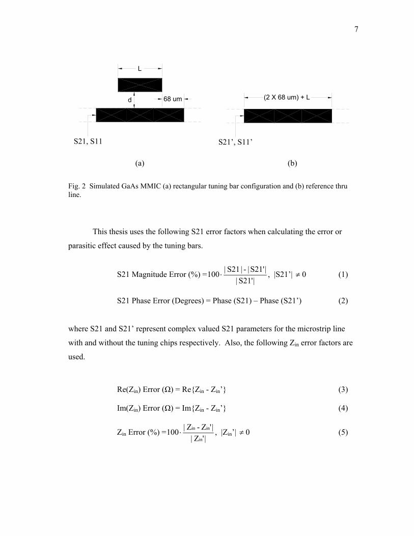
Fig. 2 Simulated GaAs MMIC (a) rectangular tuning bar configuration and (b) reference thru line.
This thesis uses the following S21 error factors when calculating the error or
parasitic effect caused by the tuning bars.
S21 Magnitude Error (%) =|S21'|
|S21' |- |S21|100 ⋅ , |S21’| ≠ 0 (1)
S21 Phase Error (Degrees) = Phase (S21) – Phase (S21’) (2)
where S21 and S21’ represent complex valued S21 parameters for the microstrip line
with and without the tuning chips respectively. Also, the following Zin error factors are
used.
Re(Zin) Error (Ω) = ReZin - Zin’ (3)
Im(Zin) Error (Ω) = ImZin - Zin’ (4)
Zin Error (%) =|'Z|
|' Z- Z|100in
inin⋅ , |Zin’| ≠ 0 (5)

8
where Zin and Zin’ represent the complex input impedance values for the microstrip line
with and without the tuning bars, respectively.
1. Matched Load
For a matched load, Zin and S21 (both primed and unprimed) are simulated in a
system with the same termination impedances as that of the microstrip thru line. For
example, when measuring Zin and S21 for a 25 Ω line, the feed lines and terminations
(both port 1 and port 2) are 25 Ω.
An error analysis is performed on the following three important cases:
1. Typical case: L = 100 um, d = 100 um, AB included. This case incorporates
standard dimensions used in practice. That is, the tuning bar is placed one
substrate height away from the line (d = 100 um) and the length of the tuning
bar is typical for circuits on GaAs. For this case, the AB is included in the
simulation.
2. Worst case specified by Raytheon: L = 200 um, d = 50 um, AB not included.
This case includes the minimum tuning bar offset distance (d = 50 um) and
maximum length (L = 200 um) specified by Raytheon for this thesis.
Raytheon expected this case to cause a large error. The AB is not included in
the simulation.
3. Absolute worst case: L = 200 um, d = 5 um, AB not included. This case
includes the minimum gap spacing that can currently be fabricated on GaAs
(d = 5 um) for the maximum specified length. The AB is not included in the
simulation.
Table I gives the simulated error results for these three cases. For convenience,
the maximum error in each category is shaded grey.

9
TABLE I SIMULATED GAAS TUNING BAR ERROR RESULTS FOR THREE IMPORTANT CASES. ERRORS
ARE FOR MATCHED LOAD (VSWR=1).
Typical case: L = 100 um, d = 100 um, AB Included
Frequency (GHz)
ReZin Error (Ω) ImZin Error (Ω) Zin Error (%) S21 Magnitude Error (%)
S21 Phase Error (Degrees)
25 Ohm (W = 256 um) 10 -0.0013 -0.0114 0.0457 -0.0006 -0.001435 -0.0152 -0.0286 0.1286 -0.0010 0.0006
50 Ohm (W = 70 um) 10 -0.0011 -0.0144 0.0288 -0.0007 0.000535 -0.0205 -0.0440 0.0951 -0.0012 0.0030
100 Ohm (W = 5 um) 10 0.0001 -0.0003 0.0003 0.0000 0.000035 0.0000 -0.0009 0.0009 -0.0001 -0.0001
Worst case specified by Raytheon: L = 200 um, d = 50 um, AB not Included
Frequency
(GHz)ReZin Error (Ω) ImZin Error (Ω) Zin Error (%) S21 Magnitude
Error (%)S21 Phase
Error (Degrees)
25 Ohm (W = 256 um) 10 -0.0193 -0.0971 0.3945 -0.0053 -0.014435 -0.2112 -0.2146 1.2200 -0.0197 -0.0333
50 Ohm (W = 70 um) 10 -0.0208 -0.1313 0.2643 -0.0057 -0.003635 -0.2879 -0.3418 0.8891 -0.0155 -0.0087
100 Ohm (W = 5 um) 10 0.0001 -0.0034 0.0033 -0.0003 -0.000335 -0.0046 -0.0082 0.0087 -0.0005 -0.0018
Absolute worst case: L = 200 um, d = 5 um, AB not Included
Frequency
(GHz)ReZin Error (Ω) ImZin Error (Ω) Zin Error (%) S21 Magnitude
Error (%)S21 Phase
Error (Degrees)
25 Ohm (W = 256 um) 10 -0.1061 -0.5161 2.0994 -0.0373 -0.235135 -1.2564 -1.1912 6.9942 -0.1773 -0.7862
50 Ohm (W = 70 um) 10 -0.1379 -0.8511 1.7138 -0.0447 -0.111235 -1.9728 -2.2362 5.9331 -0.1588 -0.3566
100 Ohm (W = 5 um) 10 -0.0007 -0.1155 0.1121 -0.0082 -0.014635 -0.2257 -0.4168 0.4413 -0.0289 -0.0382
For a matched load, the simulated results shown in Table I validate the
conventional wisdom that suggests unused tuning bars placed one substrate height away
from the thru line causes negligible effect. Moreover, if the criterion for “negligible
effect” is chosen so that the error factors, Zin and S21 magnitude error, are less than ~1%
and the S21 phase error is less than 1 degree, then the tuning bars can be placed at half a
substrate height from the line with acceptable error. For case 3 (the absolute worst case),
the error does become unacceptable for lines with characteristic impedances of 25 and

10
50 Ohms. It should also be noted that the tuning bar configurations are simulated
between 8 and 40 GHz, and for a matched load the error factors increase almost linearly
with frequency.
2. Mismatched Load
Besides tuning bar offset distance and length, the load mismatch also affects the
tuning bar error. After many simulations with different terminating impedances, some
observations are made. First, the parasitic effects caused by the tuning bars for the
mismatched case are generally higher than the matched case. Second, in some cases the
error factors do not simply increase with frequency for a given load, but rather oscillate
with frequency. Third, the error factors tend to increase as the load mismatch increases
(i.e. the VSWR increases).
To efficiently analyze the errors for the mismatched case, the following
technique is performed. First, Sonnet is used to simulate the lines with and without the
tuning bar for different tuning bar lengths (L) and offset distances (d) in a matched
system. Then the S-parameters are imported into ADS. Subsequently, using the
optimization capabilities of ADS, the maximum errors for a given frequency and VSWR
are extracted. Fig. 3 shows a screenshot of an optimization simulation performed in
ADS for the Zin error factor. Port 1 is kept matched to the line (50 Ω for the case shown
in Fig. 3) and the terminating impedance at port 2 is changed. Using the procedure
described above, it is found that the maximum error factors do increase linearly with
frequency (as opposed to varying with frequency for a single terminating impedance.)
Note that when ADS simulates for a complex load, it outputs the generalized power
scattering parameters.

11
GoalOptimGoal2
RangeMax[1]=RangeMin[1]=RangeVar[1]=Weight=Max=gamma_loadMin=gamma_loadSimInstanceName="SP1"Expr="mag(ZL5-50)/(mag(ZL5+50))"
GOAL
VARVAR5gamma_load=0.3
EqnVar
VARVAR4frequency_of_interest=35 GHz
EqnVar
VARVAR3x5=52.478 Ohms opt 0 to 99999
EqnVarVAR
VAR2y5=32.1259 Ohms opt unconst
EqnVarVAR
VAR1ZL5=x5+j*y5
EqnVar
GoalOptimGoal1
RangeMax[1]=frequency_of_interestRangeMin[1]=f requency_of_interestRangeVar[1]="f req"Weight=Max=Min=300SimInstanceName="SP1"Expr="mag(zin(S11,50)-zin(S33,50))/mag(zin(S11,50))"
GOAL
OptimOptim1
DesiredError=0.0MaxIters=25ErrorForm=L2OptimType=Gradient
OPTIM
S_ParamSP1
Step=1 GHzStop=frequency_of_interestStart=f requency_of_interest
S-PARAMETERS
TermTerm3
Z=50 OhmNum=3 S2P
50_Ohm_Length_is_100_umFile="50_ohm_200um_long_d_equals_5.snp"
21
Ref TermTerm4
Z=ZL5Num=4
S2P50_Ohm_Reference_Length_is_100_umFile="50_ohm_200um_long_reference.snp"
21
RefTermTerm1
Z=50 OhmNum=1
TermTerm2
Z=ZL5Num=2
Fig. 3 ADS optimization screenshot
The results of the error maximization procedure for the Z0 = 50 Ω and 25 Ω cases
are shown in Figs. 4 and 5. The results given are for the magnitude of the reflection
coefficient |Γ0| = 1/3 (VSWR = 2) and L = 200 um (maximum tuning bar length
analyzed in this thesis). Figs. 4 and 5 demonstrate that the error is only significant at
very small tuning bar offset distances and that the error exponentially decreases with
tuning bar offset distance. The results also show an apparent discrepancy between the Zin
and S21 magnitude error factors. For instance, in Fig. 4 the Zin error is 8 % while the
S21 magnitude error is only 0.8 %. This apparent discrepancy is simply because the
power absorbed by the load relative to the input power (which is quantified by the
magnitude of S21 squared), stays almost constant regardless of small changes to the
overall input impedance. For example, suppose the input impedance changes from Zin =
50 Ω to Zin = 54 Ω. While this corresponds to an 8% difference in input impedance, the
magnitude of S21 for the two cases is calculated to differ by only 0.074% (assuming a
lossless and reciprocal network in a 50 Ω system).

12
Z0=50 Ω
5 20 35 50 65 80 95 110 125 140
Tuning Bar Offset Distance, d (um)
0
1
2
3
4
5
6
7
8
Max
imum
Zin
Erro
r (%
)
Freq = 10 GHz Freq = 20 GHzFreq = 35 GHz
5 20 35 50 65 80 95 110 125 140
Tuning Bar Offset Distance, d (um)
0.0
0.1
0.2
0.3
0.4
0.5
0.6
0.7
0.8
Max
imum
|S21
Mag
nitu
de E
rror|
(%)
Freq = 10 GHz Freq = 20 GHzFreq = 35 GHz
(a) (b)
5 20 35 50 65 80 95 110 125 140Tuning Bar Offset Distance, d (um)
0.0
0.2
0.4
0.6
0.8
1.0
Max
imum
|S21
Pha
se E
rror|
(Deg
rees
)
Freq = 10 GHz Freq = 20 GHzFreq = 35 GHz
(c)
Fig. 4 Maximum (a) Zin, (b) |S21 magnitude|, and (c) |S21 phase| error factors. Z0 = 50 Ω, L = 200 um, substrate thickness = 100 um, and VSWR = 2.

13
Z0 = 25 Ω
5 20 35 50 65 80 95 110 125 140
Tuning Bar Offset Distance, d (um)
0
1
2
3
4
5
6
7
8
Max
imum
Zin
Erro
r (%
)
Freq = 10 GHz Freq = 20 GHzFreq = 35 GHz
5 20 35 50 65 80 95 110 125 140
Tuning Bar Offset Distance, d (um)
0.0
0.1
0.2
0.3
0.4
0.5
0.6
0.7
0.8
Max
imum
|S21
Mag
nitu
de E
rror|
(%)
Freq = 10 GHz Freq = 20 GHzFreq = 35 GHz
(a) (b)
5 20 35 50 65 80 95 110 125 140Tuning Bar Offset Distance, d (um)
0.00
0.25
0.50
0.75
1.00
1.25
1.50
Max
imum
|S21
Pha
se E
rror|
(Deg
rees
)
Freq = 10 GHz Freq = 20 GHzFreq = 35 GHz
(c) Fig. 5 Maximum (a) Zin, (b) |S21 magnitude|, and (c) |S21 phase| error factors. Z0 = 25 Ω, L = 200 um, substrate thickness = 100 um, and VSWR = 2.

14
For comparison, the maximum Zin error factors for L = 100 um and L = 150 um
are given in Figs. 6 and 7. Overall, it is seen that as the width of the line increases
(which corresponds to a decreasing Z0) the error factors also slightly increase. Also, as
one would expect, the error increases as L increases. For Z0 = 100 Ω, the error factors
are negligible (Zin error < 0.1%, S21 phase error < 0.08 degrees) and are not shown.
5 20 35 50 65 80 95 110 125 140Tuning Bar Offset Distance, d (um)
0
1
2
3
4
Max
imum
Zin
Erro
r (%
)
Freq = 10 GHz Freq = 20 GHzFreq = 35 GHz
5 20 35 50 65 80 95 110 125 140
Tuning Bar Offset Distance, d (um)
0
1
2
3
4
5
6
Max
imum
Zin
Erro
r (%
)
Freq = 10 GHz Freq = 20 GHzFreq = 35 GHz
(a) (b)
Fig. 6 Maximum Zin error factors for (a) L = 100 um and (b) L = 150 um. Substrate thickness = 100 um, Z0 = 50 Ω, and VSWR = 2.

15
5 20 35 50 65 80 95 110 125 140Tuning Bar Offset Distance, d (um)
0
1
2
3
4
5
Max
imum
Zin
Erro
r (%
)Freq = 10 GHz Freq = 20 GHzFreq = 35 GHz
5 20 35 50 65 80 95 110 125 140
Tuning Bar Offset Distance, d (um)
0
1
2
3
4
5
6
7
Max
imum
Zin
Erro
r (%
)
Freq = 10 GHz Freq = 20 GHzFreq = 35 GHz
(a) (b) Fig. 7 Maximum Zin error factor for (a) L = 100 um and (b) L = 150 um. Substrate thickness = 100 um, Z0 = 25 Ω, and VSWR = 2. 3. Resonant Frequency Error Analysis
Another method of analyzing the parasitic effects of the tuning bar is to simulate
a resonant circuit with and without the tuning bar and observe the change in resonant
frequency. The resonant frequency error is herein defined as the resonant frequency
difference between a quarter-wave stub resonant circuit with and without a tuning bar.
Fig. 8 shows the simulated quarter-wave stub resonant circuits with centered offset
rectangular tuning bars. In Fig. 8 (a) the circuit is designed to resonant at around 10
GHz and in Fig. 8 (b) the circuit resonates at 35 GHz. The AB is not included in this
analysis because its effects are particularly small.

16
2610 um
735 um
S21, S11 S21, S11
(a) (b)
Fig. 8 GaAs MMIC quarter wave stub resonant circuit at (a) 10 GHz and (b) 35 GHz with rectangular tuning bar.
Table II gives the simulated resonant frequency errors for the three cases: typical,
worst case specified by Raytheon, and absolute worst case. It is seen that the errors for
both the typical and worst case specified by Raytheon are less than 0.04% and
negligible. For the absolute worst case, the errors become slightly more significant for
the 25 Ω and 50 Ω lines, with errors ranging between around 0.1% and 0.36%.

17
TABLE II SIMULATED GAAS QUARTER WAVE STUB RESONANT FREQUENCY ERROR RESULTS FOR
THREE IMPORTANT CASES.
Typical case: L = 100 um, d = 100 um, AB Not Included
Approx. Resonant Frequency (GHz)
Resonant Frequency Error (MHz)
Resonant Frequency Error (%)
25 Ohm (W = 256 um) 10 |Error| < 1 |Error| < 0.01 35 3 |Error| < 0.01
50 Ohm (W = 70 um) 10 |Error| < 1 |Error| < 0.01 35 2 |Error| < 0.01
100 Ohm (W = 5 um) 10 |Error| < 1 |Error| < 0.01 35 |Error| < 1 |Error| < 0.01
Worst case specified by Raytheon: L = 200 um, d = 50 um, AB not Included
Approx. Resonant Frequency (GHz)
Resonant Frequency Error (MHz)
Resonant Frequency Error (%)
25 Ohm (W = 256 um) 10 |Error| < 1 |Error| < 0.01 35 14 0.04
50 Ohm (W = 70 um) 10 |Error| < 1 |Error| < 0.01 35 12 0.034
100 Ohm (W = 5 um) 10 |Error| < 1 |Error| < 0.01 35 |Error| < 1 |Error| < 0.01
Absolute worst case: L = 200 um, d = 5 um, AB not Included
Approx. Resonant Frequency (GHz)
Resonant Frequency Error (MHz)
Resonant Frequency Error (%)
25 Ohm (W = 256 um) 10 -16 -0.1635 -129 -0.369
50 Ohm (W = 70 um) 10 -9 -0.0935 -37 -0.11
100 Ohm (W = 5 um) 10 -2 -0.0235 -22 -0.062
4. Equivalent Circuit
In practice, one typically does not take the time to model the actual tuning bar
configuration. Instead, guided by conventional wisdom, the designer simply places the

18
tuning bar at a certain offset distance away from the thru line (usually a distance of about
1.0 to 1.5 substrate heights), and assumes the tuning bar’s effects are negligible. One
goal of this thesis is to test the validity of this convention and recommend a more
optimum offset distance depending on the configuration. Therefore, modeling the tuning
bar configurations is not the primary focus here. That being said, an equivalent circuit or
model does help gain more insight into the effects of the tuning bar.
The rectangular tuning bar configuration on GaAs substrate essentially involves
a microstrip thru line parallel coupled to another microstrip line section that is open
circuited at both ends. This parallel coupled transmission line circuit is shown in Fig. 9
(a). Since both the thru line and the tuning bar have the same width, the effects of the
tuning bar can be analyzed (at least approximately) through the use of even-odd mode
analysis and has the equivalent circuit shown in Fig. 9 (b) [8]. The even and odd mode
characteristic impedances of the coupled line system are denoted Z0e and Z0o,
respectively. It is seen that the equivalent circuit is simply a transmission line with the
same length as the original and with a new characteristic impedance Z0,eq = (Z0e+ Z0o)/2.
Using filter terminology, this is an all pass network. It should be noted that the
equivalent circuit is valid for TEM operation only, and it also ignores edge effects.
Therefore, the equivalent circuit only approximately models the coupled microstrip
tuning bar configuration (which supports quasi-TEM modes), and it therefore may not
accurately predict the minute turning bar errors which are reported in this thesis.

19
Z0
Z0
L
d0o0e Z,Z
(a)
Z0,eq
L
( ) 2ZZZ 0o0eeq0, +=
(b)
Fig. 9 Tuning bar configuration. (a) Coupled line section representation and (b) equivalent circuit.
From the equivalent circuit in Fig. 9 (b), it is apparent why the tuning bar error
increases with frequency. First, the electrical length of the equivalent circuit
transmission line segment increases with frequency. As the electrical length increases,
the effect on circuit performance due to the difference between the perturbed
transmission line’s characteristic impedance Z0,eq and the unperturbed transmission line’s
characteristic impedance Z0 becomes more pronounced.
Based on the tuning bar configuration’s equivalent circuit shown in Fig. 9, there
are two reasons why the parasitic errors are small. The first reason is that the tuning bars
used are electrically short. For example, the electrical length of the 200 um bars on GaAs
is only about 7 degrees at 10 GHz. The second reason is that Z0,eq and Z0 are very
similar. As an example, consider the tuning bar configuration with an offset distance d =

20
50 um (half a substrate height), operating frequency at 10 GHz, with a line characteristic
impedance of Z0 = 25 Ω. Using Txline software, the calculated characteristic impedance
of the perturbed line Z0,eq = 23.4 Ω. Therefore, it is seen that Z0,eq only deviates slightly
from Z0 (about 6%). The corresponding VSWR and |S11| (in a 50 Ohm system) are
1.016 and -41.8 dB. Therefore, the equivalent circuit model also predicts very little error
(or mismatch) attributed to the adjacent tuning bar.
Another interesting observation is that the parasitic effects of the tuning bar are
not necessarily dependent on the strength of the electromagnetic coupling as quantified
by the coupling coefficient C = (Z0e- Z0o)/ (Z0e+ Z0o). This coupling coefficient dictates
how much power can be coupled from one line to another for coupled line directional
couplers [8]. From the tuning bar configuration’s equivalent circuit, one can see that the
parasitic effects increase as the value of Z0,eq strays from the value of Z0. Because Z0,eq =
(Z0e+ Z0o)/2, the difference between Z0 and Z0,eq (which results in tuning bar error) is not
necessarily dependent on the difference between Z0e and Z0o. That is to say, the
magnitude of the tuning bar error is not necessarily dependent on the coupling
coefficient.
5. U-Shaped Tuning Bars
In practice, U-shaped (or horseshoe-shaped) tuning bars are used instead of
rectangular tuning bars if tuning bar lengths greater than 100 um are needed. Fig. 10
shows the layout of the GaAs MMIC U-shaped tuning bar configuration analyzed in this
thesis. While Fig. 10 includes an AB, the AB is not actually simulated due to enormous
computation times. The simple formula, Lpath = (⋅π r + W/2) gives the mean (average)
path length, Lpath, of the U-shaped tuning bar with an inner radius, r, and a width, W.
The effective length including the end effects is slightly larger. In this thesis r = 50 um.
Therefore, Lpath = 165 um, 267 um, and 560 um for the 100 Ω, 50 Ω, and 25 Ω cases,
respectively. Compared to the rectangular tuning bar, the length of the U-shaped tuning
bar is larger and the end effects make the effective gap size smaller.

21
100 um
Airbridge W
d
W
r
68 um
S21, S11
Fig. 10 GaAs MMIC U-shaped tuning bar configuration.
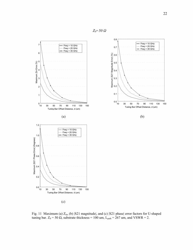
The error maximization procedure for a mismatched load is performed on the U-
shaped tuning bar configuration. The results are shown in Figs. 11 and 12 for Z0 = 50 Ω
and Z0 = 25 Ω with |Γ0| = 1/3 (VSWR = 2). Compared to the previous straight bar cases,
the errors for the U-shaped bar are worse for Z0 = 25 Ω, but almost the same for Z0 = 50
Ω. This is due to the comparatively large Lpath for the Z0 = 25 Ω case. For Z0 = 100 Ω,
the error factors are negligible and are not shown.
22
Z0=50 Ω
10 30 50 70 90 110 130 150
Tuning Bar Offset Distance, d (um)
0
1
2
3
4
5
6
7
Max
imum
Zin
Erro
r (%
)
Freq = 10 GHz Freq = 20 GHzFreq = 35 GHz
10 30 50 70 90 110 130 150
Tuning Bar Offset Distance, d (um)
0.0
0.1
0.2
0.3
0.4
0.5
0.6
0.7
0.8
Max
imum
|S21
Mag
nitu
de E
rror|
(%)
Freq = 10 GHz Freq = 20 GHzFreq = 35 GHz
(a) (b)
10 30 50 70 90 110 130 150Tuning Bar Offset Distance, d (um)
0.0
0.2
0.4
0.6
0.8
1.0
1.2
Max
imum
|S21
Pha
se E
rror|
(Deg
rees
)
Freq = 10 GHz Freq = 20 GHzFreq = 35 GHz
(c) Fig. 11 Maximum (a) Zin, (b) |S21 magnitude|, and (c) |S21 phase| error factors for U-shaped tuning bar. Z0 = 50 Ω, substrate thickness = 100 um, Lpath = 267 um, and VSWR = 2.

23
Z0=25 Ω
10 30 50 70 90 110 130 150Tuning Bar Offset Distance, d (um)
0
1
2
3
4
5
6
7
8
9
10
11
12
Max
imum
Zin
Erro
r (%
)
Freq = 10 GHz Freq = 20 GHzFreq = 35 GHz
10 30 50 70 90 110 130 150Tuning Bar Offset Distance, d (um)
0.0
0.5
1.0
1.5
2.0
2.5
3.0
3.5
4.0
Max
imum
|S21
Mag
nitu
de E
rror|
(%)
Freq = 10 GHz Freq = 20 GHzFreq = 35 GHz
(a) (b)
10 30 50 70 90 110 130 150Tuning Bar Offset Distance, d (um)
0.0
0.2
0.4
0.6
0.8
1.0
1.2
1.4
1.6
1.8
Max
imum
|S21
Pha
se E
rror|
(Deg
rees
)
Freq = 10 GHz Freq = 20 GHzFreq = 35 GHz
(c)
Fig. 12 Maximum (a) Zin, (b) |S21 magnitude|, and (c) |S21 phase| error factors for U-shaped tuning bar. Z0 = 25 Ω, substrate thickness = 100 um, Lpath = 560 um, and VSWR = 2.
24
6. Conclusions
The current practice of placing tuning bars one substrate height away from the
main thru line for GaAs MMIC’s is quite conservative. Using the results given in this
chapter allows the tuning bars to be confidently placed at shorter distances. In general
the tuning bar error increases as the load mismatch and, subsequently, the VSWR
increases. Finally, the U-shaped tuning bar results in higher error compared to the
rectangular shaped bar.
C. Thin Film Network (TFN) Tuning Bar Configurations
A study on the error associated with unused tuning bars on 10 mil (thickness)
alumina and 7.4 mil Ferro A6M substrate is performed. The two common TFN tuning
bar configurations are the line-lengthening tuning stub and the rectangular tuning chip
cluster configurations. Line-lengthening tuning stubs consist of multiple rectangular
bars offset at the end of an open microstrip line. When tuning the line (i.e. extending the
length of the open line), one simply bonds the tuning bars to the open microstrip line.
The rectangular tuning chip cluster configuration includes a number of small rectangular
bars flanking the main thru line. When tuning the line (i.e. changing the impedance of
the thru line), one bonds the tuning bars to the main thru line.
In this section, the tuning bar error is inspected for two common TFN substrate
materials, alumina and Ferro A6M. Nominal parameters for the two substrates used
throughout this section are as follows. Alumina dielectric constant; εr = 9.65, substrate
thickness = 10 mils, substrate loss tangent; tan δ = 0.001, and gold metallization
thickness = 0.1 mils. Ferro A6M dielectric constant; εr = 6.1, substrate thickness = 7.4
mils, substrate loss tangent; tan δ = 0.0012, and gold metallization thickness = 0.4 mils.
The line impedance of interest is 50 Ω. Using TX-Line for the specified parameters, the
corresponding line widths at 10 GHz for alumina and Ferro A6M are approximately 10
and 11 mils, respectively.

25
1. Line-Lengthening Tuning Stub Configuration
Fig. 13 shows the layout of the TFN line-lengthening tuning stub configuration.
As shown in the figure, the dimensions of the tuning bars are typically W × W/2, where
W is the width of the microstrip line. In practice, there can be more than three stubs and
the distances between the stubs are not necessarily equal.
W X W/2
W
Microstrip line
Fig. 13 Typical TFN line-lengthening tuning stub geometry.
When simulating, the feed line is de-embedded as shown in Fig. 14. In the
figure, two parallel dashed lines represent the de-embedded feed line. The length of the
microstrip line is equal to the width of the line. This is chosen arbitrarily and no
generality is lost by this de-embedding scheme. The distance between the microstrip line
and the first tuning bar is d1; the distance between the first and second tuning bars is d2,
etc.
W
W/2
Wd1 d2 d3
W
W1d 2d 3d
(a) (b)
Fig. 14 Simulated TFN (a) line-lengthening tuning stub configuration and (b) reference thru line after de-embedding.
S11 S11’

26
For practical purposes, only the first two tuning bars closest to the line need to be
taken into account for error analysis. To illustrate this, the line-lengthening tuning stub
configuration is simulated with one, two, four, and eight tuning bars. Fig. 15 shows the
simulated Zin error (%). The results shown in the figure are for the worst-case error (i.e.
the minimum distance that can be fabricated on these substrates). This corresponds to a
distance (d1, d2, …, d8) of 1 mil for alumina and 2 mils for Ferro A6M.
8 16 24 32 40Frequency (GHz)
0
1
2
3
4
Zin
Erro
r (%
)
One Tuning PadTwo Tuning PadsFour Tuning PadsEight Tuning Pads
8 16 24 32 40Frequency (GHz)
0.0
0.4
0.8
1.2
Zin
Erro
r (%
)
One Tuning PadTwo Tuning PadsFour Tuning PadsEight Tuning Pads
(a) (b) Fig. 15 Simulated worst-case Zin error factors for (a) alumina and (b) Ferro A6M for one, two, four, and eight line-lengthening stubs.
As Fig. 15 shows, the Zin error factor for a line-lengthening tuning stub
configuration (even with minimum distances) is dependent solely on the first two tuning
bars. In other words, the error from eight tuning bars is the same as the error from only
two tuning bars. Furthermore, it is seen that about 90% of the error is due to the first
tuning bar, and so the error is much more dependent on d1 than on d2. Because of the

27
above observations, only the first two tuning bars will be included in the following
simulations, and as a simplification, d2 is taken to equal d1 (d2 = d1 = d).
An error analysis for three important tuning bar offset distances, d, is now
performed. For alumina, d is varied as 10 mils (substrate height), 5 mils (half the
substrate height), and 1 mil (minimum distance). For Ferro A6M, d is varied as 8 mils (~
substrate height), 4 mils (~ half the substrate height), and 2 mils (minimum distance).
These cases represent the typical, compact (worse), and absolute worst case,
respectively. The results are given in Table III. As shown, the error factors are relatively
small regardless of the offset distance. Also, as expected, the errors increase as d is
decreased. This is due to increased coupling between the stub and tuning bars as d is
decreased.
TABLE III SIMULATED LINE-LENGTHENING TUNING STUB ERRORS FOR THREE IMPORTANT CASES.
Alumina
Frequency Re[Zin] Error (Ω) Im[Zin]Error (Ω) Zin Error (%)
Typical Case: d = 10 mils 10 GHz 0.000 0.127 0.04635 GHz 0.000 0.045 0.067
Compact Case: d = 5 mils 10 GHz -0.001 0.935 0.34135 GHz -0.001 0.328 0.491
Absolute Worst Case: d = 1 mils 10 GHz -0.008 8.506 3.10035 GHz -0.008 2.900 4.350
Ferro A6M
Frequency Re[Zin] Error (Ω) Im[Zin]Error (Ω) Zin Error (%)
Typical Case: d = 8 mils 10 GHz -0.001 0.237 0.07535 GHz 0.000 0.083 0.094
Compact Case: d = 4 mils 10 GHz -0.003 1.595 0.50135 GHz -0.001 0.514 0.629
Absolute Worst Case: d = 2 mils 10 GHz -0.007 5.009 1.57335 GHz -0.004 1.609 1.969
28
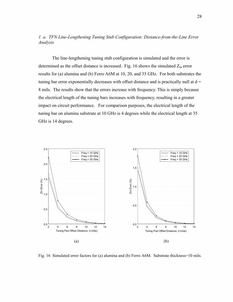
1. a. TFN Line-Lengthening Tuning Stub Configuration: Distance-from-the-Line Error Analysis The line-lengthening tuning stub configuration is simulated and the error is
determined as the offset distance is increased. Fig. 16 shows the simulated Zin error
results for (a) alumina and (b) Ferro A6M at 10, 20, and 35 GHz. For both substrates the
tuning bar error exponentially decreases with offset distance and is practically null at d =
8 mils. The results show that the errors increase with frequency. This is simply because
the electrical length of the tuning bars increases with frequency, resulting in a greater
impact on circuit performance. For comparison purposes, the electrical length of the
tuning bar on alumina substrate at 10 GHz is 4 degrees while the electrical length at 35
GHz is 14 degrees.
2 4 6 8 10 12 14Tuning Pad Offset Distance, d (mils)
0.0
0.5
1.0
1.5
2.0
2.5
Zin
Erro
r (%
)
Freq = 10 GHzFreq = 20 GHzFreq = 35 GHz
2 4 6 8 10 12 14
Tuning Pad Offset Distance, d (mils)
0.0
0.5
1.0
1.5
2.0
Zin
Erro
r (%
)
Freq = 10 GHzFreq = 20 GHzFreq = 35 GHz
(a) (b) Fig. 16 Simulated error factors for (a) alumina and (b) Ferro A6M. Substrate thickness=10 mils.

29
1.b. TFN Line-Lengthening Tuning Stub Configuration: Resonant Frequency Error Analysis
In many cases, open stubs are used as resonators in filters and oscillators. To
determine the effect of the line-lengthening tuning stub configuration on resonant stubs,
resonant circuits with and without line lengthening tuning bars are simulated and the
resonant frequency errors are found. Fig. 17 shows the perturbed quarter wave stub
resonant circuits that are simulated for alumina substrate. In Fig. 17 (a) the circuit is
designed to resonant at 10 GHz and in Fig. 17 (b) the circuit resonates at 35 GHz. The
lengths of the quarter wave stub resonant circuits for alumina at 10 and 35 GHz are 115
and 32 mils, respectively.
115 mil
32 mil
S21, S11 S21, S11
(a) (b)
Fig. 17 Quarter wave stub resonant circuit at (a) 10 GHz and (b) 35 GHz with line-lengthening tuning stubs.

30
The resonant frequency errors for the three cases (typical, compact, and absolute
worst case) are given in Table IV. For both alumina and Ferro A6m, the tuning bar error
is significant for the compact case at 35 GHz (> 0.1%). The errors are even more
significant for the absolute worst case. For example, at 35 GHz the error is almost 1.0 %
for the tuning stub configuration on alumina substrate.
TABLE IV SIMULATED TFN QUARTER WAVE STUB RESONANT FREQUENCY ERROR RESULTS FOR
THREE IMPORTANT CASES.
Alumina
Approx. Resonant Frequency (GHz)
Resonant Frequency Error (MHz)
Resonant Frequency Error (%)
Typical Case: d = 10 mils 10 |Error| <1 |Error| <0.0135 -5 -0.014
Compact Case: d = 5 mils 10 -3 -0.0335 -40 -0.11
Absolute Worst Case: d =1 mil 10 -32 -0.3235 -335 -0.957
Ferro A6M
Approx. Resonant Frequency (GHz)
Resonant Frequency Error (MHz)
Resonant Frequency Error (%)
Typical Case: d = 8 mils 10 |Error| <1 |Error| <0.0135 -5 -0.014
Compact Case: d = 4 mils 10 -3 -0.0335 -35 -0.1
Absolute Worst Case: d = 2 mils 10 -12 -0.1235 -158 -0.45
2. 6×16 mil² Rectangular Tuning Chips in a Cluster (RTCC)
The two common dimensions of the individual tuning bars comprising the TFN
RTCC configuration are 6×16 mil² and 10×10 mil². In this section, the 6×16 mil² case is

31
analyzed, and Fig. 18 shows the general layout of the 6×16 mil² RTCC configuration. In
practice, there can be more than three columns of tuning bars, more than two rows of
bars, and the bars can be on one or both sides of the microstrip thru line.
Microstrip line
Fig. 18 Typical 6×16 mil² TFN RTCC configuration.
When simulating, the feed line is de-embedded as shown in Fig. 19. In the
figure, two parallel dashed lines represent the de-embedded feed line. The length of the
microstrip thru line for both alumina and Ferro A6M extends 6 mils beyond the tuning
bar configuration in both directions to account for fringing fields. The distance between
the first row and the thru line is equal to the distance between rows of tuning bars and is
denoted d1. The distance between the columns of tuning chips is d2. Fig. 19 shows the
tuning bar pattern arranged in two rows-by-five columns flanking both sides of the line.
This thesis analyzes up to a maximum of five columns.
6×16 mil²

32
d1
d2
6 mils
W
1d
2d
S21, S11
d2
d1
W
6 mils
Fig. 19 Geometry of 6×16 mil² TFN RTCC configuration analyzed in this thesis.
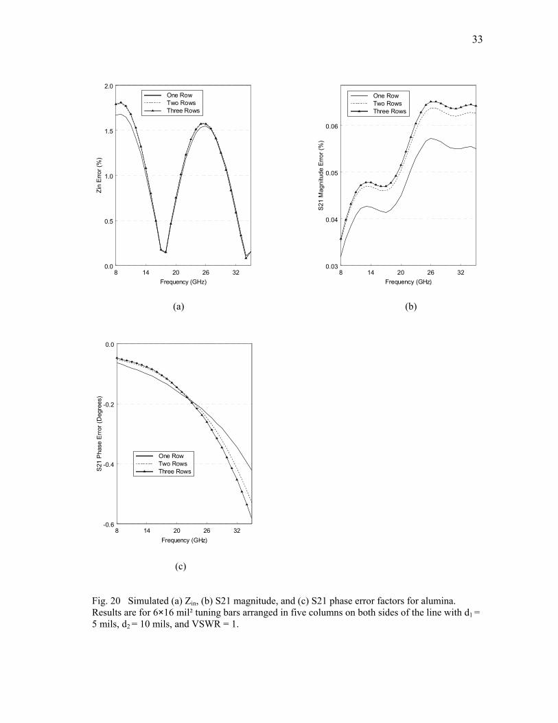
2.a. 6×16 mil² RTCC: Effect of Multiple Rows First, the effect of multiple rows of tuning bars on the tuning bar error is
investigated. The 6×16 mil² RTCC configuration is simulated on alumina containing
five columns with one, two, and three rows of tuning bars flanking both sides of the line.
This corresponds to three cases; (1) one row-by-five columns flanking both sides, (2)
two rows-by-five columns flanking both sides, and (3) three rows-by-five columns
flanking both sides. In the simulation, d1 = 5 mils, d2 = 10 mils, and Γ0 = 0 (matched
line). Fig. 20 gives the simulated results, where it is seen that the error factors are
affected mainly by the first two rows of tuning bars closest to the thru line. Furthermore,
the majority of the signal perturbation is caused by only the first row of bars closest to
the line. This is similar to the TFN line-lengthening tuning stub configuration, in which
it was found that only the first two tuning bars closest to the line need to be taken into
account for error analysis (see Fig. 15).
33
8 14 20 26 32Frequency (GHz)
0.0
0.5
1.0
1.5
2.0
Zin
Erro
r (%
)One RowTwo RowsThree Rows
8 14 20 26 32
Frequency (GHz)
0.03
0.04
0.05
0.06
S21
Mag
nitu
de E
rror (
%)
One RowTwo RowsThree Rows
(a) (b)
8 14 20 26 32Frequency (GHz)
-0.6
-0.4
-0.2
0.0
S21
Pha
se E
rror
(Deg
rees
)
One RowTwo RowsThree Rows
(c)
Fig. 20 Simulated (a) Zin, (b) S21 magnitude, and (c) S21 phase error factors for alumina. Results are for 6×16 mil² tuning bars arranged in five columns on both sides of the line with d1 = 5 mils, d2 = 10 mils, and VSWR = 1.

34
2.b. 6×16 mil² RTCC: Effect of Distance between Columns (d2)
The distance between the columns of tuning bars (d2) affects mainly the
frequency characteristics of the error factor curves. To illustrate this, an error
maximization procedure (as discussed in section B.2 of this chapter) is performed on
alumina with one row-by-five columns of tuning bars flanking both sides of the line with
d1 = 4 mils and |Γ0| = 1/3 (VSWR = 2). The simulation results are shown in Fig. 21. As
shown in the figure, the maximum (or peak) values of the error factors are relatively
close for different values of d2. It can also be seen that the error curves oscillate as a
function of frequency. The maximum values of the error factors occur approximately at
frequencies where the electrical length of the section of line adjacent to the tuning bars is
an odd multiple of 90 degrees. To illustrate, for d2 = 5 mils, the total length of line
adjacent to the tuning bars is 10045516 =⋅+⋅ mils. This has an electrical length of 90
and 180 degrees at 11.45 and 22.53 GHz, respectively. It can be seen from Fig. 21 that
these two frequencies approximately correspond to the maximum and minimum values
of the errors, respectively. Therefore, as d2 is increased, the electrical length of the line
increases, and thus the general shape of the error curves shifts to lower frequencies.
This oscillatory phenomenon can be explained by considering the equivalent
circuit of a coupled line section representation. The equivalent circuit of a coupled
section is simply an equal length transmission line with characteristic impedance Z0,eq =
(Z0e+ Z0o)/2 (see Fig. 9). Therefore the RTCC configuration is equivalent to a
transmission line with a characteristic impedance periodically alternating between Z0 and
Z0,eq. When the total effective electrical length of the perturbed line for this simple
model is 180 degrees, the input impedance approaches the load impedance. Therefore,
one would expect little error in this case. When the effective electrical length of the
perturbed line is 90 degrees, the line acts similar to a quarter wave transformer and is
thus more dependent on the effective perturbation-dependent characteristic impedance.
To more exactly explain and predict the response shown in Fig. 21, one would have to
take into account the multiple reflections at each junction between segments of
transmission line with characteristic impedance Z0 and Z0,eq.

35
8 16 24 32 40Frequency (GHz)
0
1
2
3
4
Max
imum
Zin
Erro
r (%
)d2 = 5 milsd2 = 10 milsd2 = 15 mils
8 16 24 32 40
Frequency (GHz)
-0.5
-0.4
-0.3
-0.2
-0.1
0.0
0.1
Max
imum
S21
Mag
nitu
de E
rror (
%)
d2 = 5 milsd2 = 10 milsd2 = 15 mils
(a) (b)
8 16 24 32 40Frequency (GHz)
-1.0
-0.8
-0.6
-0.4
-0.2
Max
imum
S21
Pha
se E
rror (
Deg
rees
)
d2 = 5 milsd2 = 10 milsd2 = 15 mils
(c) Fig. 21 Simulated maximum (a) Zin, (b) S21 magnitude, and (c) S21 phase error factors for alumina. Results are for 6×16 mil² tuning bars arranged as one row-by-five columns on both sides of the line with d1=4 mils and VSWR=2.

36
2.c. 6×16 mil² RTCC: Distance-from-the-Line Error Analysis
The 6×16 mil² RTCC configuration involves many variables including the
number of rows and columns, row and column offset distances, frequency, load
impedance, and layout (whether or not the tuning bars flank one or both sides of the thru
line). To simplify the analysis, the following error maximization procedure is
performed. First, d2 is kept at 5 mils for both alumina and Ferro A6M. The tuning bar
configuration is then simulated for various offset distances, d1. Next the error
maximization procedure, as described in the previous section, is performed over a
frequency range 8-40 GHz with |Γ0| = 1/3 (VSWR = 2). The maximum value of both the
Zin and S21 error factors are extracted and plotted versus tuning bar offset distance for
the frequency ranges 8-24 GHz and 24-40 GHz.
Figs. 22 and 23 give the simulated results for alumina at 8-24 GHz and 24-40
GHz, respectively. Figs. 24 and 25 give the simulated results for Ferro A6M. The S21
magnitude error factors are negligible and not shown. The results show that the error
factors decrease exponentially with offset distance d1 and are quite small- even at half a
substrate height. Also, the errors are higher for the cases where the tuning bars flank
both sides compared to the cases where the bars flank a single side. At higher
frequencies (8-24 GHz), the errors are greater for the 5 column arrangement compared to
the 3 column arrangement. Finally, it can be observed that the errors for the tuning bar
configuration on alumina substrate are only slightly larger than that on the Ferro A6M
substrate. Yet, when considering the offset distance in terms of percentage of substrate
height, the parasitic effects are slightly higher for Ferro A6M than alumina.

37
2 4 6 8 10 12 14 16 18 20Tuning Pad Offset Distance, d1 (mils)
0
1
2
3
4
5
6
7
8
Max
imum
Zin
Erro
r (%
)1 Row X 5 Columns, Both Sides1 Row X 5 Columns, Single Side1 Row X 3 Columns, Both Sides1 Row X 3 Columns, Single Side
2 4 6 8 10 12 14 16 18 20
Tuning Pad Offset Distance, d1 (mils)
0.0
0.2
0.4
0.6
0.8
1.0
Max
imum
|S21
Pha
se E
rror|
(Deg
rees
)
(a) (b)
Fig. 22 Maximum (a) Zin error factors and (b) S21 phase error factors for alumina. Results are for 6×16 mil² tuning bars with d2 = 5 mils, substrate thickness=10 mils and VSWR=2. Frequency range: 8-24 GHz.
2 4 6 8 10 12 14 16 18 20Tuning Pad Offset Distance, d1 (mils)
0
1
2
3
4
5
6
7
8
9
Max
imum
Zin
Erro
r (%
)
1 Row X 5 Columns, Both Sides1 Row X 5 Columns, Single Side1 Row X 3 Columns, Both Sides1 Row X 3 Columns, Single Side
2 4 6 8 10 12 14 16 18 20
Tuning Pad Offset Distance, d1 (mils)
0.0
0.2
0.4
0.6
0.8
1.0
1.2
1.4
1.6
1.8
2.0
Max
imum
|S21
Pha
se E
rror|
(Deg
rees
)
(a) (b) Fig. 23 Maximum (a) Zin error factors and (b) S21 phase error factors for alumina. Results are for 6×16 mil² tuning bars with d2 = 5 mils, substrate thickness=10 mils, and VSWR=2. Frequency range: 24-40 GHz.

38
2 4 6 8 10 12 14 16 18 20Tuning Pad Offset Distance, d1 (mils)
0
1
2
3
4
5
6
7
Max
imum
Zin
Erro
r (%
)
1 Row X 5 Columns, Both Sides1 Row X 5 Columns, Single Side1 Row X 3 Columns, Both Sides1 Row X 3 Columns, Single Side
2 4 6 8 10 12 14 16 18 20
Tuning Pad Offset Distance, d1 (mils)
0.0
0.2
0.4
0.6
0.8
Max
imum
|S21
Pha
se E
rror|
(Deg
rees
)
(a) (b)
Fig. 24 Maximum (a) Zin error factors and (b) S21 phase error factors for Ferro A6M. Results are for 6×16 mil² tuning bars with d2 = 5 mils, substrate thickness = 7.4 mils and VSWR = 2. Frequency range: 8-24 GHz.
2 4 6 8 10 12 14 16 18 20Tuning Pad Offset Distance, d1 (mils)
0
1
2
3
4
5
6
7
Max
imum
Zin
Erro
r (%
)
1 Row X 5 Columns, Both Sides1 Row X 5 Columns, Single Side1 Row X 3 Columns, Both Sides1 Row X 3 Columns, Single Side
2 4 6 8 10 12 14 16 18 20
Tuning Pad Offset Distance, d1 (mils)
0.0
0.2
0.4
0.6
0.8
1.0
1.2
Max
imum
|S21
Pha
se E
rror|
(Deg
rees
)
(a) (b)
Fig. 25 Maximum (a) Zin error factors and (b) S21 phase error factors for Ferro A6M. Results are for 6×16 mil² tuning bars with d2 = 5 mils, substrate thickness = 7.4 mils and VSWR = 2. Frequency range: 24-40 GHz.

39
3. 10×10 mil² RTCC
The previous section analyzed the TFN RTCC configuration comprised of
discrete tuning bars each of dimension 6×16 mil². The other common dimension of
tuning bar used in the TFN RTCC configuration is10×10 mil², which is analyzed in this
section. Fig. 26 shows the general layout of the 10×10 mil² RTCC configuration. In
practice, there can be more than three columns of tuning bars, more than one row of
bars, and the bars can be on one or both sides of the microstrip thru line.
Fig. 26 Typical 10×10 mil² TFN RTCC.
When simulating, the 10×10 mil² RTCC is de-embedded in the same manner as
the 6×16 mil² RTCC; namely, the length of the microstrip thru line for both alumina and
Ferro A6M extends 6 mils beyond the tuning bar configuration in both directions to
account for any fringing fields. Also, like the 6×16 mil² case, the distance between the
first row of tuning bars and the microstrip thru line is equal to the distance between rows
of bars and is denoted d1. The distance between the columns of tuning bars is denoted
d2.
10×10 mil²

40
3.a. 10×10 mil² RTCC: Effect of Multiple Rows
Resembling the 6×16 mil² RTCC configuration, only the first row of 10×10 mil²
tuning bars closest to the microstrip thru line cause the majority of the signal
perturbation. To illustrate this, the 10×10 mil² RTCC is simulated on alumina
containing five columns with one, two, and three rows on both sides of the line. This
corresponds to three cases; (1) one row-by-five columns flanking both sides, (2) two
rows-by- five columns flanking both sides and (3) three rows-by- five columns flanking
both sides. In the simulation, d1 = 5 mils, d2 = 10 mils, and Γ0 = 0 (matched line). Fig.
27 gives the simulated error results. It is evident from these results that the second and
third rows have almost no effect on the frequency dependence or magnitude of the error
factors and parasitic coupling. Therefore, the results of the error analysis determined
through the simulation of one row can be safely applied to the cases comprising multiple
rows. The reason is because only the tuning bars directly adjacent to the thru line couple
energy from the line. This concept is similar to that when designing microwave filters
using coupled resonators. That is, one usually only considers the coupling between
adjacent resonators in the filter, which in turn keeps the coupling matrix as sparse as
possible and simplifies the problem.

41
8 14 20 26 32
Frequency (GHz)
0
1
2
3Zi
n E
rror (
%)
One RowTwo RowsThree Rows
8 14 20 26 32
Frequency (GHz)
0.02
0.03
0.04
0.05
0.06
S21
Mag
nitu
de E
rror (
%)
One RowTwo RowsThree Rows
(a) (b)
8 14 20 26 32Frequency (GHz)
-0.6
-0.5
-0.4
-0.3
-0.2
S21
Phas
e Er
ror (
Deg
rees
)
One RowTwo RowsThree Rows
(c) Fig. 27 Simulated (a) Zin, (b) S21 magnitude, and (c) S21 phase error factors for alumina. Results are for 10×10 mil² tuning bars arranged in five columns on both sides of the line with d1=5 mils, d2=10 mils, and VSWR=1.
42
3.b. 10×10 mil² RTCC: Effect of Distance between Columns (d2)
Also, similar to the 6×16 mil² RTCC configuration, the distance between the
columns of tuning bars d2 affects mainly the frequency characteristics of the error factor
curves. To demonstrated this, an error maximization procedure is performed on alumina
with the 10×10 mil² tuning bars arranged as one row-by-five columns flanking both
sides of the line, d1=4 mils, and |Γ0| = 1/3 (VSWR=2). The simulation results are shown
in Fig. 28. As shown in the figure, the maximum (or peak) values of the error factors are
relatively close for different values of d2. Like the 6×16 mil² RTCC configuration, the
error curves oscillate as a function of frequency, and the maximum values of the error
factors occur approximately at frequencies where the electrical length of the section of
line adjacent to the tuning bars is an odd multiple of 90 degrees. The minimum values of
the error factors occur approximately at frequencies where the electrical length of the
section of line adjacent to the tuning bars is an even multiple of 90 degrees. This
oscillatory was also observed for the 6×16 mil² RTCC configuration and was explained
in section C.2.b of this chapter by considering the equivalent circuit of a coupled line
representation. Essentially, when the total effective electrical length of the perturbed line
is 180 degrees, the input impedance approaches the load impedance, and one would
expect little error. When the effective electrical length of the perturbed line is 90
degrees, the line acts similar to a quarter wave transformer and would thus exhibit a
higher error compared to the unperturbed case.
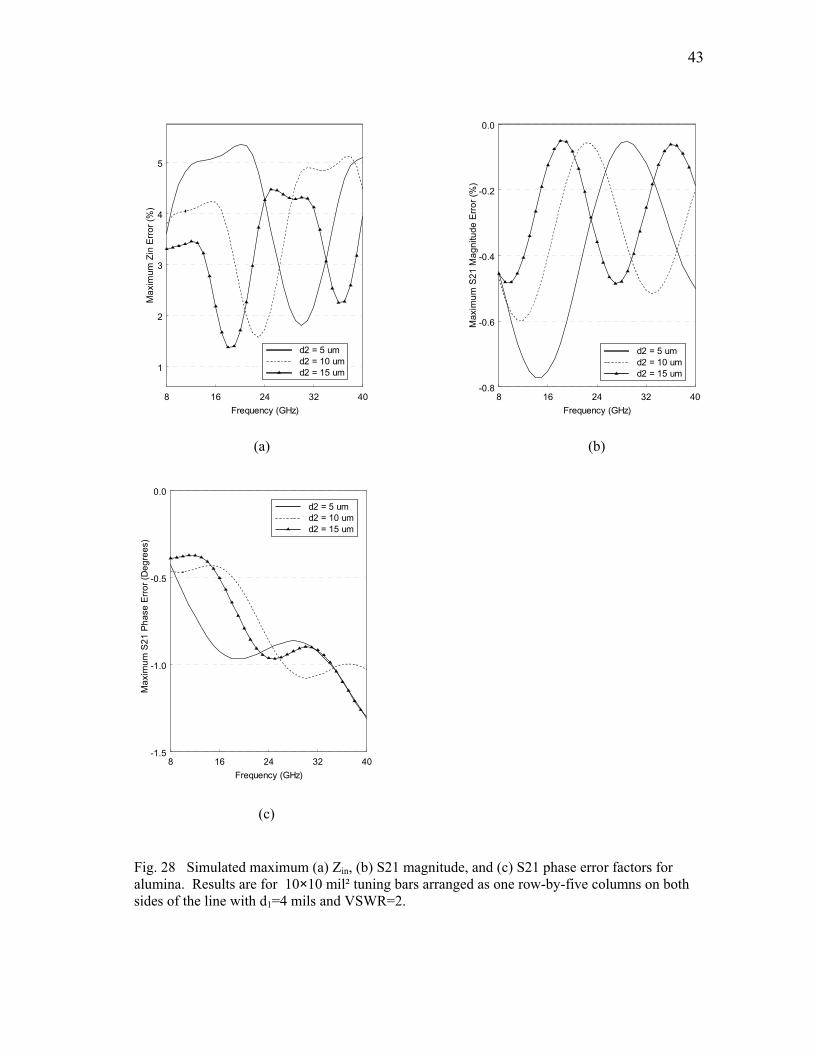
43
8 16 24 32 40
Frequency (GHz)
1
2
3
4
5M
axim
um Z
in E
rror (
%)
d2 = 5 umd2 = 10 umd2 = 15 um
8 16 24 32 40
Frequency (GHz)
-0.8
-0.6
-0.4
-0.2
0.0
Max
imum
S21
Mag
nitu
de E
rror (
%)
d2 = 5 umd2 = 10 umd2 = 15 um
(a) (b)
8 16 24 32 40Frequency (GHz)
-1.5
-1.0
-0.5
0.0
Max
imum
S21
Pha
se E
rror (
Deg
rees
)
d2 = 5 umd2 = 10 umd2 = 15 um
(c) Fig. 28 Simulated maximum (a) Zin, (b) S21 magnitude, and (c) S21 phase error factors for alumina. Results are for 10×10 mil² tuning bars arranged as one row-by-five columns on both sides of the line with d1=4 mils and VSWR=2.

44
3.c. 10×10 mil² RTCC: Distance-from-the-Line Error Analysis
The same error maximization procedure is performed on the 10×10 mil² RTCC
as the 6×16 mil² case. Namely, the tuning bar configuration is simulated for various
offset distances d1 over a frequency range 8-40 GHz with |Γ0| = 1/3. Then the maximum
values of the Zin and S21 phase errors are extracted. Figs. 29 and 30 give the simulated
results for alumina at 8-24 GHz and 24-40 GHz, respectively. Figs. 31 and 32 give the
simulated results for Ferro A6M. The S21 magnitude error factors are negligible and not
shown.
The distance-from-the-line error analyses findings for both the 6×16 mil² and
10×10 mil² RTCC show the error factors exponentially decreases with frequency.
Furthermore the error factors are similar for both alumina and Ferro A6M. In general
the S21 phase error is less than 1 degree for an offset distance d1 of half a substrate
height. These results not only confirm the validity of placing tuning bars a distance of
one substrate height (in this case the substrate thickness is 10 mils for alumina and 7.4
mils for Ferro A6M) from the line to achieve negligible error, but show this convention
is rather conservative for many instances. The errors for the 10×10 mil² cases are also
comparatively larger than the corresponding 6×16 mil² cases. It is therefore apparent
that the width of the tuning bars has more of an adverse effect on circuit performance
than the length of the bar (at least for the range of dimensions considered here). This is
similar to the error analysis findings from the tuning bar configuration on GaAs
substrate, where it was found that the errors increase for a decreasing characteristic
impedance (increasing width).

45
2 4 6 8 10 12 14 16 18 20Tuning Pad Offset Distance, d1 (mils)
0
1
2
3
4
5
6
7
8
9
10
11
12
Max
imum
Zin
Erro
r (%
)1 Row X 5 Columns, Both Sides1 Row X 5 Columns, Single Side1 Row X 3 Columns, Both Sides1 Row X 3 Columns, Single Side
2 4 6 8 10 12 14 16 18 20
Tuning Pad Offset Distance, d1 (mils)
0.0
0.2
0.4
0.6
0.8
1.0
1.2
1.4
1.6
1.8
2.0
2.2
2.4
Max
imum
|S21
Pha
se E
rror|
(Deg
rees
)
1 Row X 5 Columns, Both Sides1 Row X 5 Columns, Single Side1 Row X 3 Columns, Both Sides1 Row X 3 Columns, Single Side
(a) (b) Fig. 29 Maximum (a) Zin error factors and (b) S21 phase error factors for alumina. Results are for 10×10 mil² tuning bars with d2 = 5 mils, substrate thickness=10 mils and VSWR=2. Frequency range: 8-24 GHz.
2 4 6 8 10 12 14 16 18 20Tuning Pad Offset Distance, d1 (mils)
0
1
2
3
4
5
6
7
8
9
10
11
12
Max
imum
Zin
Erro
r (%
)
1 Row X 5 Columns, Both Sides1 Row X 5 Columns, Single Side1 Row X 3 Columns, Both Sides1 Row X 3 Columns, Single Side
2 4 6 8 10 12 14 16 18 20
Tuning Pad Offset Distance, d1 (mils)
0.00.20.40.60.81.01.21.41.61.82.02.22.42.62.83.03.23.4
Max
imum
|S21
Pha
se E
rror|
(Deg
rees
)
1 Row X 5 Columns, Both Sides1 Row X 5 Columns, Single Side1 Row X 3 Columns, Both Sides1 Row X 3 Columns, Single Side
(a) (b) Fig. 30 Maximum (a) Zin error factors and (b) S21 phase error factors for alumina. Results are for 10×10 mil² tuning bars with d2 = 5 mils, substrate thickness=10 mils and VSWR=2. Frequency range: 24-40 GHz.

46
2 4 6 8 10 12 14 16 18 20Tuning Pad Offset Distance, d1 (mils)
0
1
2
3
4
5
6
7
8
9
10M
axim
um Z
in E
rror (
%)
1 Row X 5 Columns, Both Sides1 Row X 5 Columns, Single Side1 Row X 3 Columns, Both Sides1 Row X 3 Columns, Single Side
2 4 6 8 10 12 14 16 18 20
Tuning Pad Offset Distance, d1 (mils)
0.0
0.2
0.4
0.6
0.8
1.0
1.2
1.4
1.6
Max
imum
|S21
Pha
se E
rror|
(Deg
rees
)
1 Row X 5 Columns, Both Sides1 Row X 5 Columns, Single Side1 Row X 3 Columns, Both Sides1 Row X 3 Columns, Single Side
(a) (b) Fig. 31 Maximum (a) Zin error factors and (b) S21 phase error factors for Ferro A6M. Results are for 10×10 mil² tuning bars with d2 = 5 mils, substrate thickness=7.4 mils and VSWR=2. Frequency range: 8-24 GHz.
2 4 6 8 10 12 14 16 18 20Tuning Pad Offset Distance, d1 (mils)
0
1
2
3
4
5
6
7
8
9
10
Max
imum
Zin
Erro
r (%
)
1 Row X 5 Columns, Both Sides1 Row X 5 Columns, Single Side1 Row X 3 Columns, Both Sides1 Row X 3 Columns, Single Side
2 4 6 8 10 12 14 16 18 20Tuning Pad Offset Distance, d1 (mils)
0.0
0.2
0.4
0.6
0.8
1.0
1.2
1.4
1.6
1.8
Max
imum
|S21
Pha
se E
rror|
(Deg
rees
)
1 Row X 5 Columns, Both Sides1 Row X 5 Columns, Single Side1 Row X 3 Columns, Both Sides1 Row X 3 Columns, Single Side
(a) (b) Fig. 32 Maximum (a) Zin error factors and (b) S21 phase error factors for Ferro A6M. Results are for 10×10 mil² tuning bars with d2 = 5 mils, substrate thickness=7.4 mils and VSWR=2. Frequency range: 24-40 GHz.

47
4. Mismatched Lines with High VSWR
The standing waves resulting from highly mismatched loads can lead to higher
tuning bar errors than given in the preceding analyses. This is due to the relatively high
coupling that exists between voltage and current maximums in the thru line and adjacent
tuning bars. Thus far in this thesis the largest VSWR analyzed is 2, because most
microwave circuits in post-production have low mismatches. Yet, there may be cases
with high load mismatch, and caution should be taken regarding tuning bar placement.
After many simulations with various load reflection coefficients it was found that
the TFN RTCC error is most sensitive to load mismatch compared to the other tuning
bar configurations (including the GaAs MMIC tuning bar configurations). It is therefore
recommended that the RTCC configurations be placed at points in the circuit with low
mismatch. If this cannot be done then d2 (the distance between columns of tuning bars)
can be designed so that a minimum tuning bar error falls within the frequency of interest
(see Fig. 28), or at the very least, the tuning bar offset distance d1 should be greater than
one substrate height.
5. Conclusions
In this section the error due to the TFN line-lengthening tuning stub
configuration and the RTCC configuration is analyzed for both alumina and Ferro A6M
substrates. A distance-from-the-line error analysis as well as a resonant frequency error
analysis shows that the line-lengthening tuning bars can be placed closer than one
substrate height – especially for lower frequencies. For both the line-lengthening
configuration and RTCC configuration, the tuning bars placed directly adjacent to the
microstrip line cause the majority of the error. Also, the RTCC configuration error is
sensitive to not only the distance between rows d1 but also the distance between columns
d2. A distance-from-the-line error analysis is provided for both the 6×16 mil² and 10×10
mil² RTCC configurations for various cases, and assists the design of compact tuning bar
configurations with minimum parasitic effects. Finally, it should be noted that higher

48
mismatch loads lead to higher tuning bar errors due to the increased coupling between
the tuning bars and thru line.
D. Measurements and Experimental Validation
To demonstrate the accuracy of Sonnet and the simulation settings used in this
chapter, measurements are made on microstrip quarter-wave stub resonators and
compared to simulated results. The resonators are fabricated on Duroid 6010.5 using the
etching facilities available at the Department of Electrical Engineering at Texas A&M
University and measured on the Hewlett-Packard 8510C Network Analyzer.
1. Circuit Layout
An open circuit quarter-wave stub resonant circuit is fabricated on Duroid 6010.5
(εr = 10.5) with a substrate height of 10 and 25 mils, and the exact replicas are simulated
using Sonnet. The circuit layout for the resonator (a) without tuning bars and (b) with
tuning bars is shown in Fig. 33 for a substrate height h of 10 mils. The 10×10 mil²
tuning bars are arranged in two vertical columns with five rows flanking both sides of
the line. The offset distances between both rows and columns of tuning bars are equal to
8 mils (minimum distance allowed due to fabrication tolerances). For the resonator with
h = 25 mils, the tuning bars are arranged as described above, except, due to the increased
substrate height, the dimensions of the bars are 24×24 mil² to preserve the ratio between
substrate height and tuning bar dimensions.

49
(a) (b)
Fig. 33 Layout of measured stub resonator (a) with and (b) without tuning bars. εr = 10.5, h = 10 mils. Note: 50 Ω feedlines extend farther than shown.
2. Measurements
Fig. 34 shows the measured and simulated S21 curves for the simple resonator
without the tuning bars for (a) h=10 mils and (b) h=25 mils. For both substrate heights,
the measured and simulated results agree quite well, with the resonant frequencies
differing by only about 15 MHz. Also, as expected, the insertion loss is higher for the
measured set due to connector losses and mismatch and non-ideal metallization effects
(such as conductor surface roughness).

50
6.6 6.8 7.0 7.2 7.4 7.6 7.8 8.0 8.2 8.4 8.6 8.8 9.0 9.2 9.4Frequency (GHz)
-40
-30
-20
-10
S21
(dB
)
MeasuredSimulated
(a)
6.6 6.8 7.0 7.2 7.4 7.6 7.8 8.0 8.2 8.4 8.6 8.8 9.0 9.2 9.4Frequency (GHz)
-40
-30
-20
-10
S21
(dB
)
MeasuredSimulated
(b)
Fig. 34 Simulated vs. measured S21 curve of a stub resonator for (a) h=10 mils and (b) h=25 mils. εr=10.5.
The (a) measured and (b) simulated S21 curves for the resonator with and
without the tuning bars are shown in Fig. 35 for h = 10 mils and Fig. 36 for h = 25 mils.

51
For both cases, the simulation agrees in general with the measured resonant frequency
shift caused by the tuning bars. To accurately measure such a small effect, the resonant
circuit with tuning bars is first measured. Then, with the circuit still connected to the test
fixture, the tuning bars are carefully removed using a fine blade and microscope, and the
resulting resonant circuit, void of tuning bars, is measured a second time. It can be
observed that the frequency shift is larger in the measurements as compared to that in
simulation. This may be due to a discrepancy between conductor thickness, offset
distance, or dielectric constant between the circuit simulated (and expected) and that
actually fabricated.
7.6 7.8 8.0 8.2 8.4 8.6Frequency (GHz)
-35
-30
-25
-20
-15
S21
(dB
)
No Tuning PadsWith Tuning Pads
7.6 7.8 8.0 8.2 8.4 8.6Frequency (GHz)
-40
-35
-30
-25
-20
-15S
21 (d
B)
No Tuning PadsWith Tuning Pads
(a) (b) Fig. 35 (a) Measured and (b) simulated resonant circuit with and without the tuning bars. εr=10.5, h=10 mils.

52
7.7 7.9 8.1 8.3 8.5 8.7Frequency (GHz)
-40
-35
-30
-25
-20
-15
S21
(dB
)No Tuning StubWith Tuning Stub
7.7 7.9 8.1 8.3 8.5 8.7Frequency (GHz)
-40
-35
-30
-25
-20
-15
S21
(dB
)
No Tuning PadsWith Tuning Pads
(a) (b) Fig. 36 (a) Measured and (b) simulated resonant circuit with and without the tuning bars. εr=10.5, h=25 mils. 3. Conclusions
In this section, the accuracy of Sonnet to simulate the effect of unused tuning
bars was demonstrated by comparing both measurement and simulation of a quarter-
wave open stub resonator with and without tuning bars. Sonnet accurately predicted the
resonant frequency of the quarter-wave stub as well as the small resonant frequency shift
caused by the tuning bars. The same general Sonnet simulation settings used to simulate
in this section are used throughout the chapter.
E. Recommendations and Conclusions
1. Summary
Microwave circuit designs frequently employ tuning bars to allow the impedance
or length of a microstrip line to be adjusted in post production. In GaAs MMIC design,

53
the tuning configuration is comprised of an airbridge with a single rectangular or
horseshoe-shaped tuning bar adjacent to the main thru line. In MMIC module (or TFN)
design, both the line-lengthening tuning stub and rectangular tuning chip configurations
are used. The line-lengthening tuning stub configuration consists of multiple rectangular
bars offset at the end of an open microstrip line, and the rectangular tuning chip
configuration consists of rectangular metal patterns flanking the main thru line.
To nullify the parasitic effects of the tuning bars, conventional wisdom suggests
placing the bars 1.0 to 1.5 substrate heights away from the main line. While successful
in the past, this practice may not result in the most efficient and cost-effective placement
of tuning bars in today’s compact microwave circuits. This thesis facilitates the design
of compact tuning pad configurations with minimum parasitic effects by analyzing the
error attributable to GaAs MMIC and alumina/Ferro A6M TFN tuning pad
configurations with parameters and offset distances specified by Raytheon.
The error factors of the tuning bar configurations, which characterize the
deviation from the unaffected case in the transmission of a signal along the perturbed
line, were determined by electromagnetic simulations using Sonnet. After the lines with
and without tuning pads were simulated in Sonnet, the resulting S-parameters were
imported into ADS, where ADS’s optimization capabilities were employed to find the
maximum tuning pad error factors for a specified VSWR and frequency. The accuracy
of these simulations was verified through experimental measurements.
This thesis not only validates the conventional practice of placing tuning bars 1.0
to 1.5 substrates height from the main line, but for many cases finds this practice to be
quite conservative. For example, the GaAs MMIC tuning bar configuration has a very
small effect on circuit performance even when the tuning bar is only half a substrate
height away from the main thru line. Also, in general, the parasitic effects of the tuning
bars decrease exponentially with offset distance. Finally, highly mismatched loads result
in higher tuning bar parasitic effects due to increased coupling between thru line and the
tuning bars. This phenomenon was found most prominent for the TFN rectangular
tuning chip configuration.

54
2. Recommendations
To achieve a negligible effect, recommended tuning bar offset distances are given
in this section based on this chapter’s error analysis findings with VSWR ≤ 2. The
criterion for “negligible effect” is chosen so that the error factors, Zin and S21 magnitude
error, are less than ~1% and the S21 phase error is less than 1 degree. Note that if
VSWR > 2 then the recommendations may not hold, because, in general, the parasitic
effects of the tuning bars increases as the load mismatch increases.
Table V gives the recommended offset distances for both the rectangular and U-
shaped (horseshoe-shaped) GaAs MMIC tuning bars. As Table V shows, the lower the
characteristic impedance (the wider the line), the greater the tuning bar offset distance
should be. Also, the rectangular shaped tuning bars can safely be placed closer to the
thru line than the U-shaped bars. The recommendations are based on a substrate height
of 100 um, a rectangular tuning bar length less than 200 um, and a U-shaped tuning bar
inner radius equal to 50 um.
Both the TFN line lengthening and rectangular tuning chip configurations were
analyzed for alumina (substrate height = 10 mils) and Ferro A6M (substrate height = 7.4
mils). Overall, the parasitic effects of the tuning bars were just slightly higher for Ferro
A6M than alumina when considering the offset distance in terms of percentage of
substrate height. Table VI gives the recommended offset distances for the line-
lengthening tuning stub configuration.

55
TABLE V RECOMMENDED GAAS MMIC TUNING BAR OFFSET DISTANCES.
Rectangular-shaped
Z0 (Ω) Frequency Band
Recommended Offset Distance (% of Substrate Height)
25 X,Ku,K 55Ka 65
50 X,Ku,K 45Ka 60
100 X,Ku,K <30Ka <30 U-shaped
Z0 (Ω) Frequency Band
Recommended Offset Distance (% of Substrate Height)
25 X,Ku,K 70Ka 80
50 X,Ku,K 55Ka 70
100 X,Ku,K <30Ka <30

56
TABLE VI RECOMMENDED TFN LINE-LENGTHENING TUNING STUB OFFSET DISTANCES.
Substrate Frequency
BandRecommended Offset Distance
(% of Substrate Height)Alumina X,Ku,K 55
Ka 65Ferro A6M X,Ku,K 65
Ka 80
Table VII gives the recommended offset distances for the TFN rectangular tuning
chip configuration with tuning bar dimensions 6 × 16 mil² and 10 × 10 mil².
Comparatively, the 10 × 10 mil² tuning bars cause higher signal perturbation and should
be placed farther from the thru line. Recommendations are based on the case
comprising of one row–by–five columns with a column spacing of 5 mils. Simulation
results indicate that multiple rows have little effect, since tuning bars directly adjacent to
the thru line cause the majority of the parasitic effects. Therefore, these
recommendations hold for rectangular tuning chip configurations with more than one
row of tuning bars.

57
TABLE VII RECOMMENDED TFN RECTANGULAR TUNING CHIP CONFIGURATION OFFSET DISTANCES.
Tuning Bar Dimensions: 6 × 16 mil²
Substrate Layout Frequency Band
Recommended Offset Distance (% of Substrate Height)
Alumina Single Side X,Ku,K 60Ka 70
Double Side X,Ku,K 80Ka 85
Ferro A6M Single Side X,Ku,K 70Ka 70
Double Side X,Ku,K 90Ka 95
Tuning Bar Dimensions: 10 × 10 mil²
Substrate Layout Frequency Band
Recommended Offset Distance (% of Substrate Height)
Alumina Single Side X,Ku,K 75Ka 75
Double Side X,Ku,K 95Ka 95
Ferro A6M Single Side X,Ku,K 80Ka 80
Double Side X,Ku,K 100Ka 100

58
CHAPTER III
COMPACT RESONATORS USING THE TRANSMISSION LINE
APPROACH OF NEGATIVE REFRACTIVE INDEX
METAMATERIALS*
A. Introduction
Electromagnetic wave propagation through periodic structures has been
extensively studied for decades [9] with various applications in microwaves and optics
such as masers, traveling-wave tubes, microwave filter networks, phase shifters,
antennas, and photonic band gap structures [8], [10]. In the 1950’s and 1960’s, lattices
of discrete metallic elements were applied to the design of lightweight microwave
antenna lenses [11]. Because the periodic spacing and element dimensions are on a scale
much smaller than a wavelength, these so-called artificial dielectrics can be considered
an effective medium. Accordingly, the macroscopic electromagnetic properties of the
structures can be described by an effective electric permittivity and magnetic
permeability. Recently artificial composite materials exhibiting a negative effective
permittivity and permeability have been developed. Such a medium, also referred to as a
negative refractive index (NRI) medium, was first realized using an array of metal posts
and split-ring resonators [12],[13]. Since then, other realizations of NRI media have
been developed by various means such as using embedded magnetodielectric spherical
particles [14] and L-C loaded transmission lines [15].
In 1968, Veselago first theoretically investigated the electrodynamics of a
medium with a simultaneous negative real permittivity and permeability [16]. He
described such materials as “left-handed” since the electric field E, magnetic field H,
___________ *Part of the data reported in this chapter is reprinted with permission from “Compact gap coupled resonator using negative refractive index microstrip line” by A.D. Scher, C.T. Rodenbeck, and K. Chang, 2004. Electronics Letters, vol. 40, pp. 126-127. Copyright 2004 by The Institution of Electrical Engineers (IEE).

59
and wave vector k form a left-handed triplet as opposed to a right-handed triplet for
ordinary materials. Consequently, in this medium the phase velocity is opposite to the
direction of power flow, and all phenomena connected to the phase of the wave is
reversed including a reversed Doppler shift and backward Cherenkov radiation [16],
[17]. Additionally, the medium has a negative index of refraction – a defining
characteristic of media exhibiting both a negative permittivity and permeability [18].
The renewed interest in NRI media stems from the work of Pendry [19]-[21] as well as
the first direct measurement of a negative index of refraction [16] confirming Veselago’s
original predictions over three decades later.
To quantitatively demonstrate the counterintuitive phenomena associated with an
NRI medium, consider first a lossless electromagnetic dielectric with real permittivity ε
and real permeability µ. The Maxwell curl equations are
HE ωµj−=×∇ (6)
EH ωεj=×∇ (7)
Solving the curl equations (6) and (7) for the E and H field vectors of a plane wave in the
usual manner gives
)exp( rkEE 0 ⋅−= j (8)
)exp()(1 rkEkH 0 ⋅−= j×ωµ
(9)
where 0E is the polarization vector. Substituting (8) and (9) into (6) and (7) gives
HEk ωµj=× (10)
EHk ωεj−=× (11)

60
For a conventional medium with positive µ and ε, (10) and (11) mean the vectors k, E,
and H form a right-handed triplet, and, consequently, k points in the direction of power
flow as given by the Poynting vector S where
HES ×= (12)
Yet it also follows from (10) and (11) that if both µ and ε are negative, the wave vector k
turns in the opposite direction and k, E, and H form a left-handed set [16]. This means
the phase velocity of the plane wave is opposite to the direction of power flow. In the
cases where only one of the µ or ε is negative and the other positive, k is imaginary and
the wave does not propagate [17].
To illustrate the concept of negative refraction, consider a uniform plane wave
incident upon a dielectric interface between a conventional medium M1 ( )0, 11 >MM µε
and a backward-wave medium M2 ( )0, 22 <MM µε as shown in Fig. 37. The wavevectors
for medium M1 and M2 are k1 and k2, respectively. Snell’s law requires that the
tangential wavevector components ky1 and ky2 must equal across the interface.
Furthermore, the conservation of energy requires that the normal components of the
Poynting vectors S1 and S2 remain in the same direction (i.e. the positive x-direction in
Fig. 37) for both media. Because M2 is a backward-wave medium, kx2 is antiparallel to
the x-component of S2. Therefore, it follows that k2 is directed towards the interface and
the power is refracted through a negative angle to the normal as shown in Fig. 37 [16].

61
kx1
ky1
k1
kx2
ky2
k2
S1S2
M1 M2(µ1,ε1 > 0) (µ2,ε2 < 0)
y
x
Fig. 37 An NRI medium refracts an incident plane wave at a negative angle with the surface normal. B. The Transmission Line Approach to NRI Metamaterials
At nearly same time, two independent research groups, one at UCLA and the
other at the University of Toronto, introduced the transmission line (TL) approach of
NRI metamaterials [22], [23]. In this approach either one or two-dimensional planar
NRI media can be realized by periodically loading a transmission line with series
capacitors and shunt inductors. The TL approach has several inherent advantages
including being both low-loss and broadband [15]. Additionally, it lends itself well for
fabrication using established planar circuit technologies such as microstrip. By means of
tuning the phase response of the loaded TL, this approach has lead to improvements in
conventional RF/microwave circuit designs. Examples include branch-line couplers
operating at two arbitrary frequencies [24], broadband compact hybrid couplers [25], and
broadband compact phase shifters [26]. While this chapter only analyzes the one-

62
dimensional NRI TL structure, the concepts involved are easily extendable to two-
dimensions [27], [28].
The one-dimensional composite NRI TL unit cell is shown in Fig. 38. The
structure consists of a conventional host TL (such as a microstrip line) symmetrically
loaded with discrete lumped components, LN and CN. The host TL, composed of two
segments, has a total length d, a characteristic impedance CLZ =0 , and propagation
constant LCTL ωβ = where L and C are the TL inductance and capacitance per unit
length, respectively.
LNZ0, βTL Z0, βTL
2CN 2CNd/2 d/2
Fig. 38 One-dimensional composite NRI TL unit cell.
The complete dispersion relation for the NRI TL is determined in the well-known
manner by computing the [ABCD] matrix of the unit cell and applying Bloch-Floquet
periodic boundary conditions [15]
⎟⎟⎠
⎞⎜⎜⎝
⎛−=
NNTLBloch CL
dd 2411)cos()cos(
ωββ
NNNN
TL CLLZ
ZCd 2
0
0 41
221)sin(
ωωωβ −⎟⎟
⎠
⎞⎜⎜⎝
⎛++ (13)

63
where βBloch is the Bloch propagation constant and LCTL ωβ = is the propagation
constant of the host TL. Homogeneity requires that both the physical length of the TL
and the phase shift per unit cell be sufficiently small πβ 2( <<dTL and )2πβ <<dBloch .
When the homogeneity conditions are met, the dispersion relation of (13) can be
simplified and solved for the Bloch propagation constant βBloch which is also considered
the medium’s effective propagation constant effβ [29]
⎟⎟⎠
⎞⎜⎜⎝
⎛−⎟⎟
⎠
⎞⎜⎜⎝
⎛−±≈
dLC
dCL
NNeff 22
11ωω
ωβ (14)
In a similar manner (i.e. by computing the [ABCD] matrix of the unit cell and applying
Bloch-Floquet periodic boundary conditions) the medium’s effective characteristic
impedance effZ can be defined under the homogeneity conditions
⎟⎟⎠
⎞⎜⎜⎝
⎛−
⎟⎟⎠
⎞⎜⎜⎝
⎛−
≈
N
Neff
LC
CL
Z
2
2
1
1
ω
ω (15)
Having both effβ and effZ we can now define the effective permittivity effε and
permeability effµ for this medium as [29]
Neff
effeff L
CZ 2
1ωω
βε −== (16)
N
effeffeff C
LZ
2
1ωω
βµ −== (17)

64
The negative root for effβ in (14) is chosen for frequencies where 0, <effeff µε . This
occurs at frequencies less than the eigenfrequency 1cf where [30]
⎟⎟⎠
⎞⎜⎜⎝
⎛=
CLLCf
NNc
ππ 21,
21min1 (18)
The positive root for effβ in (14) is chosen for frequencies where 0, >effeff µε . This
occurs at frequencies greater than the eigenfrequency 2cf where [30]
⎟⎟⎠
⎞⎜⎜⎝
⎛=
CLLCf
NNc ππ 2
1,2
1max2 (19)
In the frequency range 21 cc fff << , effβ is purely imaginary and the structure presents a
stopband (analogous to an evanescent mode in a lossless waveguide). This stopband can
be closed by equating 1cf and 2cf corresponding to the following matching condition
[15]
N
N
CL
CLZ ==0 (20)
Under this condition, the effective propagation constant effβ of (14) simplifies to
dCLLC
NNeff ω
ωβ 1−+≈ (21)

65
This expression reveals that under matched conditions, the effective propagation
constant of the composite NRI TL is the sum of the propagation constants of the host TL
and an ideal L-C backward-wave line.
The complete dispersion relation of (13) is plotted in Matlab using the program
nri_tl_displot.m which is included in Appendix A. The program numerically evaluates
the right hand side (RHS) of (13) for a given frequency set and parameters. When the
RHS is unity or less, a passband exists and dBlochβ is solved by taking inverse cosine of
the RHS. When the RHS is greater than unity, a stopband exists, resulting in a gap in the
dispersion diagram. Figs. 39 and 40 show the dispersion diagrams for an unmatched
( )NN CLZ ≠0 and matched ( )NN CLZ =0 NRI TL unit cell, respectively. For both
cases the host TL has a characteristic impedance Ω= 500Z and an electrical length d =
0.176 radians (10 degrees) at 1 GHz. In the unmatched case the lumped element values
are LN = 10 nH and CN = 8 nH. In the matched case the lumped element values are LN =
15 nH and CN = 6nH.
The dispersion diagram for the unmatched case shown in Fig. 39 reveals a band
structure with two distinct stopbands and passbands. The first stopband exists for
frequencies below the cutoff frequency ( )NNb CLf π1= [15] and is due to the high-
pass nature of the loaded TL. The first passband occurs at 1cb fff << . This passband
supports backward waves [15], meaning the group velocity βω ddvg /= is opposite to
the phase velocity βω /=pv [31]. Thus, for power flow in the positive z direction, the
group velocity will be positive while the phase velocity (and consequently β ) is
negative. This is the NRI band where 0, <effeff µε and where the negative root for effβ in
(14) is chosen. As discussed previously, a stop band exists for 21 cc fff << . As the
frequency increases beyond 2cf , the effects of the lumped elements decrease and the
phase velocity approaches the phase velocity of the host TL [30]. This is the positive
refractive index (PRI) band where 0, >effeff µε and where the positive root for effβ in
(14) is selected as in the case for a conventional unloaded TL. For the matched case, as

66
shown in Fig. 40, the stopband is closed and a seamless transition exists between the
NRI and PRI regions. The transition frequency 0f between the NRI and PRI regions
occurs when 0=effβ and is given by ( ) ( )NN CLLCf ππ 21210 == [30]
fc1
fc2
fb
3.5
3
2.5
2
1.5
1
0.5
0
fc2
fc1
fb−π −π/2 π/20 π
Freq
uenc
y (G
Hz)
βBloch (radians)
Fig. 39 Dispersion diagram for the NRI TL of Fig. 38 for the unmatched case 0ZCL NN ≠ .
fb
f0
3.5
3
2.5
2
1.5
1
0.5
0−π −π/2 π/20 π
Freq
uenc
y (G
Hz)
βBloch (radians)
f0
fb
Fig. 40 Dispersion diagram for the NRI TL of Fig. 38 for the matched case 0ZCL NN = .

67
In general, the dispersion relation of (13) has an infinite number of solutions
given by [32]
,20 d
nn
πββ += ....,2,1,0 ±±=n (22)
where nβ is propagation constant of the nth mode or harmonic and 0β is the
fundamental propagation constant of the wave. This is a universal property of axially
periodic structures and is governed by Floquet’s Theorem. It follows that wave
propagation through periodic structures can be regarded as a superstition of an infinite
number of waves with different phase velocities nnv βω /= which get numerically
smaller for larger values of n [32]. Each traveling wave (called space harmonics or
Hartree harmonics [33]) has an appropriate coefficient or amplitude governed by the
boundary conditions. The effects of spatial harmonics on the operating characteristics of
the NRI TL have only begun to be studied in detail [34]. However, we know the higher
order spatial harmonics are usually only significant near band edges, which are
characterized by points on the dispersion diagram with zero slope corresponding to the
onset of a stop band [35]. Consequently, the single dominant mode n = 0 is sufficient to
accurately describe the field for the matched periodic NRI TL in the passband —
especially under homogeneity conditions.
C. Compact Zeroth-Order Resonators Using NRI Microstrip Line
Zeroth-order gap coupled line and ring resonators using NRI microstrip line are
designed based on the theory presented in the previous section and experimentally
measured. The resonators are considered “zeroth order” because at resonance the
effective electrical length of the artificial NRI line is zero. The concept of designing
subwavelength resonators using NRI metamaterials was first theoretically investigated in
[36] for a general 1-D cavity resonator. The work presented here goes further by
detailing the design and measurement of two practical implementations of
subwavelength resonators on microstrip using the TL approach of NRI metamaterials.

68
Compared to conventional resonators, the proposed resonators provide the advantages of
harmonic suppression and considerable size reduction.
1. Line Resonators [37]
Fig. 41 shows a schematic diagram of the proposed gap coupled line resonator.
The resonator is constructed with a single composite PRI/NRI TL unit cell having an
effective electrical length (net phase shift) βeffl of zero degrees at resonance where l is
the net length of the resonator. This is achieved through the use of (21) by designing the
NRI TL phase advance to equal to the PRI TL phase lag under the matching conditions
specified by (20). The resonator is designed for a resonant frequency of 1.2 GHz and
fabricated on RT/Duroid 5870 substrate with a thickness of 0.508 mm (20 mils) and a
dielectric constant of 2.23. Panasonic surface mount chip capacitors (1.0 × 0.5 mm²) and
inductors (1.6 × 0.8 mm²) are used in the design of the gap coupled loaded TL which
consists of conventional 50 Ω microstrip PRI TLs on each side of a single NRI TL cell.
The gap size is 0.2 mm. The NRI TL cell is implemented symmetrically with two series
capacitors of value 12 pF and one shunt inductor of value 15 nH. The total length of the
PRI microstrip TLs is 10.21 mm resulting in an overall resonator length of 12.09 mm.
For comparison, the length of a conventional gap coupled line half-wavelength resonator
at 1.2 GHz is 88.14 mm.

69
2CN 2CN
LNgap gap
port 1 port 2
βeffl = 0
Fig. 41 Schematic diagram of the zeroth order NRI gap coupled line resonator
The proposed PRI/NRI line resonator and a conventional gap coupled resonator
are measured using a using an Agilent 8510C network analyzer. Fig. 42 shows a
photograph of the fabricated conventional and proposed PRI/NRI gap coupled
resonators. The size of the proposed resonator is 86% more compact than that of the
conventional one. Measurement results are shown in Fig. 43. The proposed resonator
suppresses higher order frequency harmonics up to about 6.5 GHz. Past 6.5 GHz the
self-resonant frequency of the lumped components limit the operation of the resonator.
The measured loaded Q of the conventional resonator is 132 and the Q of the proposed
resonator is 48. As expected, the Q for the lumped inductor, which equals
approximately 50 at 1.2 GHz, bounds the Q of the proposed resonator. Therefore, if a
higher Q is required, a lower loss inductor should be used.

70
Fig. 42 Photograph of the proposed line resonator circuit (top) compared to a conventional gap coupled resonator (bottom)at 1.2 GHz.
1 2 3 4 5 6frequency, GHz
-100
-80
-60
-40
-20
mag
nitu
de, d
B
S21
Fig. 43 Measured results for proposed and conventional gap coupled line resonators
—— proposed - - - - conventional

71
2. Ring Resonators
Fig. 44 shows the layout of the compact ring resonator containing a single NRI
unit cell. To reduce the curvature effect of the microstrip line, the resonator is
implemented using a rectangular loop with chamfered corners. The NRI TL unit cell
consists of a section of the microstrip line symmetrically loaded with two series
capacitors each of value NC2 and one shunt inductor of value NL . Like the line
resonator, the values of CN and LN for the ring resonators are designed to satisfy the
matching conditions given in (20). Shown below in Fig. 44 (b) is a rectangular loop. At
resonance, the total effective electrical length (net phase delay) of the closed loop is zero
degrees and occurs when L Uθ = -θ where θU and θL are the phase delays for the upper and
lower paths, respectively. This condition for resonance is illustrated in Fig. 44 (b).
LN
2CN2CN
port 1 W port 2
l1
W
d
ss
(a)
upper path, θU
lower path, θL= -θU (b)
Fig. 44 (a) Layout and (b) condition for resonance for ring resonator using an NRI TL section

72
The proposed ring structure also resonates even with an inner diameter of zero.
The layout of the resonator for this case is shown in Fig. 45 and has the same structure as
that in Fig. 44 devoid of chamfered corners and with zero interior area. While not
having the conventional ring shape, this resonator is still considered a ring resonator in
that at resonance it satisfies the same condition as the NRI ring resonator with an inner
diameter greater than zero. Namely, at resonance the phase delay of the upper path 'Uθ
equals the phase advance of the lower path 'L-θ as illustrated in Fig. 45 (b).
2CN 2CN
LN
l2
W
Wport 1 port 2b2W
s s
(a)
lower path, θL= -θU
upper path, θU’
’ ’
(b)
Fig. 45 (a) Layout and (b) condition for resonance for ring resonator with an inner diameter of zero using an NRI TL section
The proposed NRI ring resonators shown in Figs. 44 and 45 are designed for a
resonant frequency of 1.2 GHz. Both are fabricated on 0.508 mm (20 mil) thick

73
RT/Duroid 5870 substrate with a relative dielectric constant of 2.33. The chip
components include Panasonic surface mount capacitors (1.0 × 0.5 mm) of value 2CN =
12 pF and inductors (1.6 × 0.8 mm) of value LN = 15 nH. The dimensions of the
resonator with an inner diameter greater than zero as shown in Fig. 44 are l1 = 6.2mm, W
= 1.47mm, and d = 1.02mm. The dimensions of the resonator with an inner diameter of
zero as shown in Fig. 45 are l2 = 6.93mm and W = 1.47mm. The coupling gap spacing
for both resonators is s = 0.2 mm.
Measurements are made using an Agilent 8510C network analyzer and the results
are shown in Fig. 46. The measured responses of the proposed resonators are almost
identical. The loaded Q for both resonators is about 48, which approximately equals the
Q for the lumped inductor at 1.2 GHz. Therefore, if the design requires a higher Q, a
lower loss inductor can be used. At 1.2 GHz, the proposed resonator offers 6 dB lower
insertion loss (for the same gap spacing) and has a maximum dimension 32% more
compact than the gap coupled NRI line resonator presented previously. Compared to a
conventional half-wavelength ring resonator at 1.2 GHz, the total circumference of the
proposed resonator (including both upper and lower paths) is reduced by 84%. As
expected, there are no higher-order resonances as in the conventional ring resonator.

74
1.0 1.5 2.0 2.5
frequency, GHz
-80
-70
-60
-50
-40
-30
mag
nitu
de, d
B
Fig. 46 Measured results for proposed ring resonators
D. Conclusions
In this chapter, the concepts related to negative refractive index technology and
techniques where reviewed and applied to the design of compact microwave resonators.
The compact NRI line resonator was found to be 86% more compact than that of the
conventional one. Furthermore, the maximum dimension of the NRI ring resonator was
32% more compact than that of the NRI line resonator. It is also demonstrated that the
ring resonator resonates even with an inner diameter of zero. Additionally, both the line
and ring NRI resonators presented herein suppress higher order resonances (harmonics).
—— inner diameter greater than zero - - - - inner diameter equal to zero

75
CHAPTER IV
SUMMARY AND RECOMMENDATIONS FOR FUTURE STUDY
A. Summary
Modern RF and microwave wireless systems usually require circuit
minimization, which leads to cost reduction. Hence, size reduction is a major design
consideration for practical applications. This thesis covers two separate topics in which
both contribute the area compact microwave circuit design.
The first topic involves determining the distance that post production tuning bars
should be from the microstrip thru line to cause a negligible effect when they are not
used. To nullify the parasitic effects of the tuning bars, conventional wisdom suggests
placing the bars 1.0 to 1.5 substrate heights away from the main line. This thesis puts
this conventional wisdom to the test by systematically analyzing the error attributable to
common GaAs MMIC and alumina/Ferro A6M TFN tuning bar configurations for a
range of offset distances. The analysis was carried out primarily using a commercially
available, numerical electromagnetic simulator due to its accuracy, practicality, and
adaptability to the various tuning bar geometries. Distance-from-the-line curves as well
as recommended offset distances are provided to facilitate the tuning bar placement with
minimum parasitic effects on the circuit. It turns out that the conventional offset
distance of 1.0 to 1.5 substrate heights is rather conservative for many cases, and
therefore does not result in the most efficient and cost-effective placement of the tuning
bars. In fact, negligible coupling exists at offset distances between 0.5-0.7 substrate
heights for many configurations.
Also in this thesis, subwavelength line and ring resonators using an NRI TL
section have been realized. Resonance occurs when the effective length of the loaded
TL equals zero degrees. The advantages of the new resonators over their conventional
counterparts include both considerable size reduction and harmonic suppression. It is
expected that the new resonators will find new applications in the design of compact
microstrip filters and oscillators.

76
B. Recommendations for Future Study
The tuning bar configurations, dimensions, and substrates analyzed in this thesis
were specified by Raytheon Company. It is therefore recommended that other common
tuning bar configurations and parameters be examined, so that a more comprehensive list
of recommended offset distances can be tabulated and available to the circuit designer.
Additionally, for certain applications, power efficient MEMs switches could be used
instead of bond wire to connect the thru line to the tuning chip. To determine the
parasitic effects on circuit performance, this requires a study of the coupling between the
open MEMs switch and tuning bar.
Another area that deserves future study is the use of the proposed NRI resonators
for practical applications including filters or oscillators. The small size of the resonators,
alone, may lead to novel designs. For example, a conventional ring resonator could
physically encircle one or more of the NRI ring resonators which may lead to new and
compact cross-coupled filters.

77
REFERENCES
[1] Sonnet Software, Inc. Sonnet 8.52, Liverpool, NY. 2002.
[2] J.D. Guill “A Study of Microstrip T-Junction Discontinuity Effects and
Modeling on GaAs Substrates”. Masters Thesis, Department of Electrical
Engineering. Texas A&M University. College Station. December 1999.
[3] Zeland Software, Inc. IE3D 10.02, Fremont, CA. 2003.
[4] Agilent Technologies, Advanced Design System 2003A, Palo Alto, CA.
[5] Applied Wave Research. (June 2003). TX-Line 2001. [Online]. Available:
http://www.appwave.com/products/txline.html.
[6] Zeland Software, Inc., (June 2003). LineGuage Basic. [Online]. Available:
http://www.zeland.com/freeware.html.
[7] K. Chang, RF and Microwave Wireless Systems. New York: Wiley, 2000.
[8] D.M. Pozar, Microwave Engineering, 2nd ed. New York: Wiley, 1998.
[9] L. Brillouin, Wave Propagation in Periodic Structures, 2nd ed. New York:
Dover, 1953.
[10] J.-F. Kiang, Novel Technologies for Microwave and Millimeter-Wave
Applications, Boston: Kluwer, 2004.
[11] M.-K. Hu, D. Cheng, “A new class of artificial dielectrics,” in WESCON/58
Conf. Rec., vol. 2, Aug. 1958, pp.21-25.
[12] D.R. Smith, W.J. Padilla, D.C. Vier, S.C. Nemat-Nasser, and S. Schultz,
“Composite medium with simultaneously negative permeability and
permittivity,” Phys. Rev. Lett., vol. 84, no. 18, pp. 4184-4187, 2000.
[13] R.A. Shelby, D.R. Smith, and S. Schultz, “Experimental verification of a
negative index of refraction,” Science, vol. 292, pp. 77-79, 2001.
[14] C.L. Holloway, E.F. Kuester, J. Baker-Jarvis, and P. Kabos, “A double negative
(DNG) composite medium composed of magnetodielectric spherical particles
embedded in a matrix,” IEEE Trans. Antennas Propogat., vol. 51, pp. 2596-2603,
Oct. 2003.

78
[15] G.V. Eleftheriades, A.K. Iyer, and P.C. Kremer, “Planar negative refractive index
media using periodically L-C loaded transmission lines,” IEEE Trans. Microwave
Theory Tech., vol. 50, pp. 2702-2712, Dec. 2002.
[16] V.G. Veselago, “The Electrodynamics of substances with simultaneously negative
values of ε and µ ,” Sov. Phys. Usp., vol 10, pp 509-514, Jan. 1968.
[17] B. Szentpáli, “Metamaterials: A new concept in the microwave technique,”
TELSIKS 2003, vol. 1, pp. 127-132, Oct. 2003.
[18] D.R. Smith, N. Kroll, “Negative Refractive Index in Left-Handed Materials,”
Phys. Rev. Lett., vol. 85, no. 14, pp. 2933-2936, Oct. 2000.
[19] J.B. Pendry, “Negative refraction makes a perfect lens,” Phys. Rev. Lett., vol. 85,
no. 18, pp. 3966-3969, 2000.
[20] J.B. Pendry, A.J. Holden, D.J. Robbins, and W.J. Stewart, “Magnetism from
conductors and enhanced nonlinear phenomena,” IEEE Trans. Microwave Theory
Tech., vol. 47, pp. 2075-2081, Nov. 1999.
[21] ———, “Low-frequency plasmons in thin wire structures,” Phys. Condens.
Matter, vol. 10, pp. 4785-4809, 1998.
[22] C. Caloz, H. Okabe, T. Iwai, and T. Itoh, “Transmission line approach of left-
handed (LH) materials,” USNC/URSI National Radio Science Meeting, San
Antonio, TX, June 2002.
[23] A.K. Iyer and G.V. Eleftheriades, “Negative refractive index metamaterials
Supporting 2-D waves,” IEEE-MTT-S Int’l Symp. Digest, pp. 1067-1070, Seattle,
WA, June 2002.
[24] L.I-Hsiang, C. Caloz, and T. Itoh, “A branch-line coupler with two arbitrary
operating frequencies using left-handed transmission lines,” IEEE-MTT-S Int’l
Symp. Digest, pp. 325-328, June 2003.
[25] H. Okabe, C. Caloz, and T. Itoh, “A compact enhanced-bandwidth hybrid ring
using an artificial lumped-element left-handed transmission-line section,” IEEE
Trans. Microwave Theory Tech., vol. 52, pp. 798-804, March 2004.

79
[26] M. Anioniades, and G.V. Eleftheriades, “Compact linear lead/lag metamaterial
phase shifters for broadband applications,” IEEE Antennas Wireless Propagat.
Lett., vol. 2, pp. 103-106, 2003.
[27] A. Grbic and G.V. Eleftheriades, “Periodic analysis of a 2-D negative refractive
index transmission line structure,” IEEE Trans. Antennas Propogat., vol. 51, pp.
2604-2611, Oct. 2003.
[28] A. Sanada, C. Caloz, T. Itoh, “Planar distributed structures with negative
refractive index,” IEEE Trans. Microwave Theory Tech., vol. 52, pp. 1252-1263,
April 2004.
[29] A. Grbic and G.V. Eleftheriades, “Experimental verification of backward-wave
radiation from a negative refractive index metamaterial,” J. Appl. Phys., vol. 92,
no. 10, pp. 5930-5935, Nov. 2002.
[30] C. Caloz, A. Sanada, T. Itoh, “A novel composite right-/left-handed coupled-line
directional coupler with arbitrary coupling level and broad bandwidth,” IEEE
Trans. Microwave Theory Tech. vol. 52, pp. 980-992, March 2004.
[31] S. Ramo, J.R. Whinnery, and T. Van Duzer, Fields and Waves in Communication
Electronics, 3rd ed. New York: Wiley, 1994.
[32] J.C. Slater, Microwave Electronics, Princeton, NJ: D. Van Nostrand and Co.
1950.
[33] R. Chatterjee, Elements of Microwave Engineering, New York: Wiley, 1986.
[34] S. Sudhakaran, Y. Han, C.G. Parini, “An experimental verification of spatial
harmonics on negative refraction,” IEEE-AP-S Symp. Digest, vol. 4, pp. 3757-
3760, June 2004.
[35] R.E. Collin, F.J. Zucker, Antenna Theory Part 2, New York: McGraw-Hill, 1969.
[36] N. Engheta, “An idea for thin subwavelength cavity resonators using
metmaterials with negative permittivity and permeability,” IEEE Antennas
Wireless Propagat. Lett., vol. 1, pp. 10-13, 2002.

80
[37] A.D. Scher, C.T. Rodenbeck, K. Chang, “Compact gap coupled resonator using
negative refractive index microstrip line,” Electron. Lett., vol. 40, pp. 126-127,
Jan. 2004.

81
APPENDIX A
MATLAB CODE FOR GENERATING NRI TL DISPERSION
DIAGRAM

82
%nri_tl_displot.m %Purpose: To calculate and plot the dispersion diagram of a lossless NRI TL % unit cell. LN=0.01*10^-9; %Lumped element inductance (H) CN=1*10^-12; %Lumped element capacitance (F) Z0=20; %Host TL characteristic impedance (Ohms) TL_beta_d_at_operating_freq=10; %Host TL electrical length (Degrees) operating_freq=1*10^9; %Operating Frequency for TL_beta_d (Hz) freq=(0.01:.005:9)*10^9; %Frequency range to plot (Hz) %Determine host TL propagation constant over frequency range of interest: freq=transpose(freq); TL_beta_d=(pi/180)*(TL_beta_d_at_operating_freq/operating_freq)*freq; %RHS of dispersion relation: arg=cos(TL_beta_d).*(1-1./(4*(2*pi)^2*(freq).^2*LN*CN))... +sin(TL_beta_d).*(1./(2*2*pi*freq*CN*Z0)+Z0./(2*2*pi*freq*LN))... -1./(4*(2*pi)^2*(freq).^2*LN*CN); NRI_beta_d=acos(arg); %Solve dispersion equation freq=freq/10^9; %Convert frequency to GHz %Determine which data points are real (propagating) or imaginary (stop %band) and store this information in an array called 'immatrix': immatrix=0; for n=1:size(NRI_beta_d) immatrix(n,1)=isreal(NRI_beta_d(n)); end sizeofdataset=size(freq); if immatrix(sizeofdataset(1,1))==1 & immatrix(1,1)==1 casenum=1; %if both first and last number in betad is real we have case #1. elseif immatrix(sizeofdataset(1,1))==1 & immatrix(1,1)==0 casenum=2; %if first number in betad is imaginary and last number is real we have %case #2. elseif immatrix(sizeofdataset(1,1))==0 & immatrix(1,1)==1 casenum=3; %if first number in betad is real and last number is immaginary we have %case #3. elseif immatrix(sizeofdataset(1,1))==0 & immatrix(1,1)==0 casenum=4; %if both first and last number in betad is immaginary we have case #4. end plotpnts=[]; %The matrix 'plotpnts' will contain the range of points (real beta_d) to plot.

83
if casenum==1 | casenum==3 plotpnts(1)=1 ; %Since the first number is real in cases 1 and 2, we start ploting from %this point. end for n=2:sizeofdataset(1,1)-1 sizepp=size(plotpnts); if immatrix(n,1)==0 & immatrix(n-1,1)==1 %Get point of transition from real to %imaginary plotpnts(sizepp(1,1)+1,1)=n-1; end if immatrix(n,1)==1 & immatrix(n-1)==0 %Get point of transition from imaginary to %real plotpnts(sizepp(1,1)+1,1)=n; end end sizepp=size(plotpnts); %Update size of 'plotpnts' if casenum==1 | casenum==2 plotpnts(sizepp(1,1)+1,1)=sizeofdataset(1,1); %Since the last number is real in cases %1 and 2 we plot up to this point end sizepp=size(plotpnts); %Update size of 'plotpnts' clf; close; %clears and closes current figures hold on; %enables multiple plots in same figure for n=1:2:sizepp(1,1) %plot for positive beta_d plot(NRI_beta_d(plotpnts(n,1):plotpnts(n+1,1)),... freq(plotpnts(n,1):plotpnts(n+1,1)),... 'k','LineWidth',2) end for n=1:2:sizepp(1,1) %plot for negative beta_d plot(-NRI_beta_d(plotpnts(n,1):plotpnts(n+1,1)),... freq(plotpnts(n,1):plotpnts(n+1,1)),... 'k','LineWidth',2) end box on axis([-pi,pi,0,max(freq)]) ylabel('Frequency (GHz)') xlabel('\beta_B_l_o_c_hd (radians)') set(gca,'XTick',-pi:pi/2:pi) set(gca, 'xticklabel', '-p | -p/2 | 0 | p/2 | p', 'fontname','symbol');

84
VITA
Aaron David Scher was born in Seattle, Washington on May 27, 1981. In May of
2003 he received a Bachelor of Science degree in electrical engineering summa cum
laude from Texas A&M University in College Station, Texas. Subsequently, he started
his M.S. degree in electrical engineering at Texas A&M University under the direction of
Dr. Kai Chang in the Electromagnetics and Microwave Laboratory. He spent the
summer of 2004 working at Southwest Research in San Antonio, Texas at their Signal
Exploitation and Geolocation Division. During the spring of 2005, he was a teaching
assistant which involved teaching the laboratory section of an undergraduate electric
circuit theory class. Aaron’s permanent address is: 4501 Michelle Dr. Arlington, TX
76016.