Embed Size (px)
Citation preview
Microstrip-Coupled TES Bolometers for CLOVER
Michael D. Audley1,*, Dorota Glowacka1, David J. Goldie1, Vassilka N. Tsaneva1, Stafford Withington1, Paul K. Grimes2, Chris North2, Ghassan Yassin2, Lucio Piccirillo3, Giampaolo Pisano3, Peter A.R. Ade4, Philip
Mauskopf4, Rashmi V. Sudiwala4, Jin Zhang4, Kent D. Irwin5, Mark Halpern6, Elia Battistelli6 1Cavendish Laboratory, University of Cambridge, JJ Thomson Ave, Cambridge, CB3 0HE, UK
2Department of Physics, University of Oxford, Denys Wilkinson Building, Keble Road, Oxford, OX1 3RH, UK 3School of Physics and Astronomy, The University of Manchester, Sackville Street Building, Manchester, M60 1QD, UK
4School of Physics and Astronomy, Cardiff University, 5, The Parade, Cardiff, CF24 3YB, UK 5National Institute of Standards and Technology, 325 Broadway, MC 817.03, Boulder, CO 80305-3328, USA
6University of British Columbia, Department of Physics and Astronomy, 6224 Agricultural Rd., Vancouver, B.C., V6T 1Z1, Canada
* Contact: [email protected], phone +44-(0)1223-337 309
Abstract— Cℓover aims to detect the signature of gravitational waves from inflation by measuring the B-mode polarization of the cosmic microwave background. We have produced microstrip-coupled TES detectors for Cℓover. The dark NEP of these detectors is dominated by the fundamental phonon-noise limit and we have measured high optical detection efficiencies in these devices with two completely different RF architectures: a finline transition and a four-probe OMT. Cℓover consists of two telescopes: one operating at 97 GHz, and one with a combined 150/220-GHz focal plane. The 220- and 150-GHz detectors use waveguide probes while the 97-GHz detectors use finline transitions to couple waveguide modes into the microstrip. Each detector is fabricated as a single chip to ensure a 100% operational focal plane. The detectors are mounted in eight-pixel modules and the focal planes are populated using 12 detector modules per detection frequency. Each detector module contains a time-division SQUID multiplexer to read out the detectors. Further amplification of the multiplexed signals is provided by SQUID series arrays. We describe the design of the Cℓover detectors and present measurements of the prototype detectors' performance showing that they satisfy the requirement of photon-noise limited operation on Cℓover.
I. INTRODUCTION
A. Scientific Motivation Thomson scattering of radiation in the early Universe can
lead to linear polarization [1] in the cosmic microwave background (CMB). The polarization depends on density fluctuations, and thus carries cosmological information which is complementary to the well-studied temperature anisotropies of the CMB. The linear polarization may be decomposed into a curl-free part and a divergence-free part, denoted E- and B-mode respectively. By measuring the B-mode polarization of the CMB with Cℓover we hope to make an indirect detection of a background of primordial gravitational waves [2], [3].
B. Key Features of Cℓover The Cℓover experiment is described in detail elsewhere
[4]. Cℓover consists of two telescopes measuring operating at frequencies of 97, 150, and 220 GHz. The low-frequency (LF) telescope observes at 97 GHz and the high-frequency (HF) telescope has a combined 150/220-GHz focal plane. Cℓover will be sited at Pampa la Bola in Chile's Atacama Desert.
For such sensitive measurements, Cℓover requires detectors with low enough NEP so that the instrument NEP is dominated by unavoidable sources of background photon noise (2.2×10⁻¹⁷ W/√Hz at 97 GHz). To achieve this sensitivity Cℓover uses bolometers with superconducting transition edge sensors (TES) [5] operating with a bath temperature of 100 mK. Cℓover's two focal planes contain hexagonal arrays of corrugated feedhorns. Orthomode transducers (OMT) separate the signal collected by each horn into two polarisations. In the LF telescope waveguide OMTs divide the two polarisations from each horn between two rectangular waveguides which each feed a finline-coupled detector. The high frequency channels use polarisation-sensitive detectors of a different architecture: four rectangular probes in a circular waveguide.
Rather than fabricating monolithic arrays we decided to make individual detectors so that we could guarantee a 100% functioning focal plane, which is important for meeting the sensitivity requirement. Also, because the detectors are much smaller than the horns in the focal plane, a monolithic array would have large, inactive areas between detectors, which would make fabrication of the detectors extremely inefficient.
Because of the large number of TESs to be read out (192 at each frequency) we use time-domain multiplexing in order to have a manageable number of wires from room temperature. The TESs are read out by 1×32 SQUID
19th International Symposium on Space Terahertz Technology, Groningen, 28-30 April 2008
143
multiplexers [6], [7], [8] fabricated by the National Institute of Standards and Technology (NIST). Further amplification is provided at the cold end by SQUID series arrays [9], also fabricated by NIST.
All the multiplexer chips in each of Cℓover's two telescopes share address lines, significantly reducing the number of wires needed to room temperature. The Nyquist inductors, which provide antialiasing filtering, and the shunt resistors that provide voltage biasing, are contained in separate chips. All of these chips are mounted on a PCB at 100 mK and connections are made to the detectors by aluminium wire bonds. The SQUID series arrays are mounted in eight-chip modules which provide the necessary magnetic shielding. Because of their higher power dissipation (1 µW per series array compared with 16 nW per multiplexer chip) these modules are heat-sunk to the still of the dilution refrigerator and they are connected to the multiplexer PCB with superconducting NbTi twisted pairs. Room-temperature multi-channel electronics (MCE) developed by the University of British Columbia, provides SQUID control and readout as well as TES bias [10]. Cℓover's MCE is similar to that used by SCUBA-2 [11].
C. Cℓover Detector Requirements For maximum sensitivity, we require that the detectors be
background-limited, i.e. the contributions to the noise equivalent power (NEP) from the detectors and readout must be less than the NEP due to unavoidable sources of photon noise:
NEPdet2 + NEPro
2 ≤ NEPphoton2.
To satisfy this requirement comfortably, we set a target for the combined NEP of the detectors and readout at 75% of the photon NEP.
Once the detectors are background-limited, the only way to improve the sensitivity is to increase the number of detectors. 96 pixels are needed at each frequency to meet Cℓover's sensitivity requirements. The LF instrument has two finline detectors per pixel (one for each polarisation). In the HF instrument there is one polarisation-sensitive OMT detector chip per pixel which measures both orthogonal polarisations. Thus, the LF instrument has 192 finline detectors and the HF instrument has a total of 192 planar OMT detectors. We require a detector time constant faster than 1 ms to satisfy the science requirements and slower than 40 µs for Nyquist sampling by the readout.
Also, the detectors must be able to absorb the power incident from the sky without saturation. This power is variable and depends on the weather. The power-handling requirement is for the detectors to be able to operate for 75% of the time at the site. We have allowed a 70% margin on this to account for uncertainties in the sky background at the site. The detector requirements are summarised in Table .
TABLE I
CℓOVER DETECTOR REQUIREMENTS AT THE THREE OPERATING FREQUENCIES.
Centre Frequency (GHz) 97 150 220
Band (GHz) 82—112 127—172 195—255 Number of pixels 96 96 96 NEP (10-17 W/√Hz) 2.2 3.7 6.7
Power Handling (pW) 11.4 20 32
II. DETECTOR ARCHITECTURE
A. TES Design Cℓover uses microstrip-coupled TES bolometers. RF
power is carried to the bolometer by a microstrip which is terminated by a matched resistor. In this resistor the RF power is dissipated as heat which is detected by the TES. We chose this architecture because Cℓover has strict requirements on sensitivity and on cross-polarization (<-35 dB). Cℓover has been designed with careful attention to minimising cross-polarisation using corrugated horns and waveguides. The microstrip-coupled TES architecture allows us to couple to the waveguides with higher efficiency than a free-space absorber would give. The microstrip coupling also gives us great flexibility by separating the bolometer from the part that couples to the waveguide. This means that we can optimise the TES without affecting the absorber, and vice versa. In Cℓover we have been able to use similar TESs with entirely different RF architectures (finline and waveguide-probes). It is also easy to inject DC power or pulses through the microstrip, which is useful for calibration.
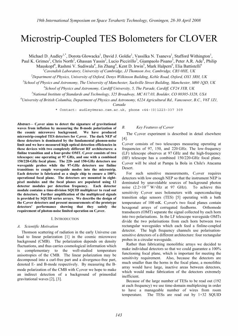
Cℓover's bolometers are on low-stress silicon nitride islands suspended by four legs for thermal isolation (see Figs 1 andFig. 2). The nitride is 0.5 µm thick. The thermal conductance to the thermal bath is controlled by the four nitride legs. A microstrip carries RF power to the bolometer and is terminated by a 23-Ω AuCu resistor which dissipates the incoming power as heat that the TES can detect. A shunt resistor in parallel with the TES ensures that it is voltage biased so that it operates in the regime of strong negative electrothermal feedback. For example, if the temperature drops, so does the resistance of the TES. Since it is biased at constant voltage, this means that the current, and hence the Joule power, will increase, heating up the TES. Conversely, if the temperature increases the resistance will increase, reducing the current, and thus the Joule heating. This means that the TES operates at a bias point that is in a stable equilibrium. Thus, the TES is self-biasing, and the electrothermal feedback speeds up the response of the detector and cancels out temperature fluctuations, which has the effect of suppressing the noise.
19th International Symposium on Space Terahertz Technology, Groningen, 28-30 April 2008
144
Fig. 1 Scanning electron microscope image of Cℓover prototype bolometer silicon nitride island showing TES and microstrip leading to termination resistor.
Fig. 2 Optical microscope image of Cℓover prototype bolometer silicon nitride island showing TES and microstrip leading to termination resistor.
The TES films in Cℓover are Mo/Cu proximity-effect bilayers with normal copper banks to define the edges of the TES. The transitions of the bilayers can be made as sharp as 1—2 mK for high sensitivity. We can also tune the transition temperature (Tc) of the films to the desired value by choosing the film thicknesses. The transition temperature Tc and thermal conductance of Cℓover's detectors are chosen to meet the NEP and power-handling requirements. All of Cℓover's detectors operate with a bath temperature of 100 mK. The 97- and 150-GHz detectors have Tc=190 mK, while the 220-GHz detectors have Tc=430 mK.
Cooling is provided by a Cryomech pulse-tube cooler, a high-capacity Chase Research He-7 cooler, and a miniature dilution refrigerator [12].
B. 97-GHz RF Design To reach background-limited sensitivity Cℓover's
bolometers must have a high absorption efficiency. Cℓover's
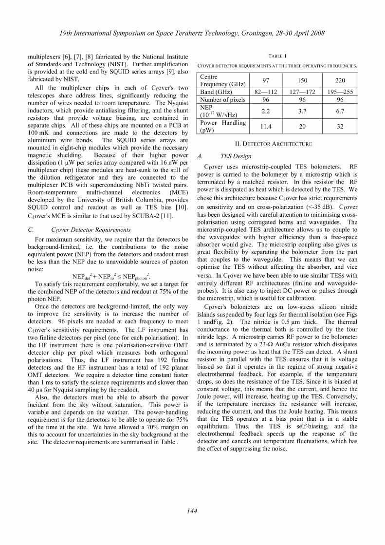
97-GHz detectors use finline transitions to couple to the radiation in the waveguide. Power is coupled from the waveguide to the TES planar circuit using an antipodal finline taper consisting of two superconducting fins of Nb separated by 400 nm of SiO2 [13], [14] (see 3 ). The lower Nb layer is 250 nm thick. The upper layer is 500 nm thick to ensure reliable lift-off patterning with the step over the oxide layer. The whole structure is deposited on one side of a 225-µm silicon substrate. Before the fins overlap, the thickness of the SiO2 is much less than that of the silicon and the structure behaves as a unilateral finline. As the fins overlap, the structure starts to behave like a parallel-plate waveguide with an effective width equal to the overlap region. When the width of the overlap region becomes large enough for fringing effects to be negligible, a transition to a microstrip mode is performed. The microstrip is then tapered to the required width. Cℓover uses a 3-µm Nb microstrip with a characteristic impedance of 23 Ω to deliver power to the TES.
The detector chip's 225-µm silicon substrate loads the waveguide in which it sits, changing the waveguide impedance. To prevent reflections the chip has a tapered end which provides a gradual impedance transition. The first set of prototype detectors use a WR-10 waveguide and have a taper angle of 40º. This angle was chosen based on detailed electromagnetic modelling.
Fig. 3 Layout of prototype 97-GHz Cℓover detector chip.
C. 97-GHz Prototype Detectors Fig. shows prototype 97-GHz Cℓover detector chips
fabricated on a 2'' wafer. Deep reactive ion etching (DRIE) is used to etch the well for the silicon nitride island and to define the outline of each chip. All of the processing of these detectors is carried out by the Detector Physics Group at the Cavendish Laboratory except for the DRIE [15].
After DRIE the chips are held in place in the wafer by small silicon tabs which can be easily broken to remove the chips.
19th International Symposium on Space Terahertz Technology, Groningen, 28-30 April 2008
145
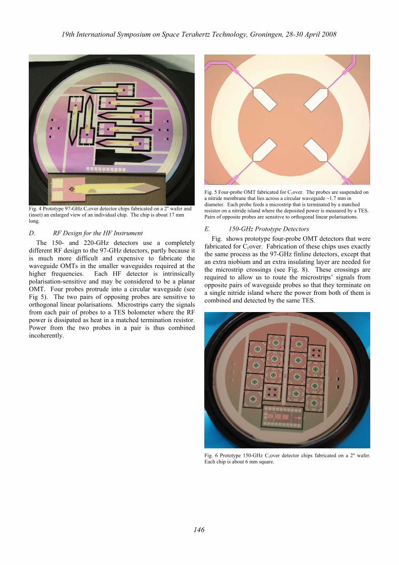
Fig. 4 Prototype 97-GHz Cℓover detector chips fabricated on a 2'' wafer and (inset) an enlarged view of an individual chip. The chip is about 17 mm long.
D. RF Design for the HF Instrument The 150- and 220-GHz detectors use a completely
different RF design to the 97-GHz detectors, partly because it is much more difficult and expensive to fabricate the waveguide OMTs in the smaller waveguides required at the higher frequencies. Each HF detector is intrinsically polarisation-sensitive and may be considered to be a planar OMT. Four probes protrude into a circular waveguide (see Fig 5). The two pairs of opposing probes are sensitive to orthogonal linear polarisations. Microstrips carry the signals from each pair of probes to a TES bolometer where the RF power is dissipated as heat in a matched termination resistor. Power from the two probes in a pair is thus combined incoherently.
Fig. 5 Four-probe OMT fabricated for Cℓover. The probes are suspended on a nitride membrane that lies across a circular waveguide ~1.7 mm in diameter. Each probe feeds a microstrip that is terminated by a matched resistor on a nitride island where the deposited power is measured by a TES. Pairs of opposite probes are sensitive to orthogonal linear polarisations.
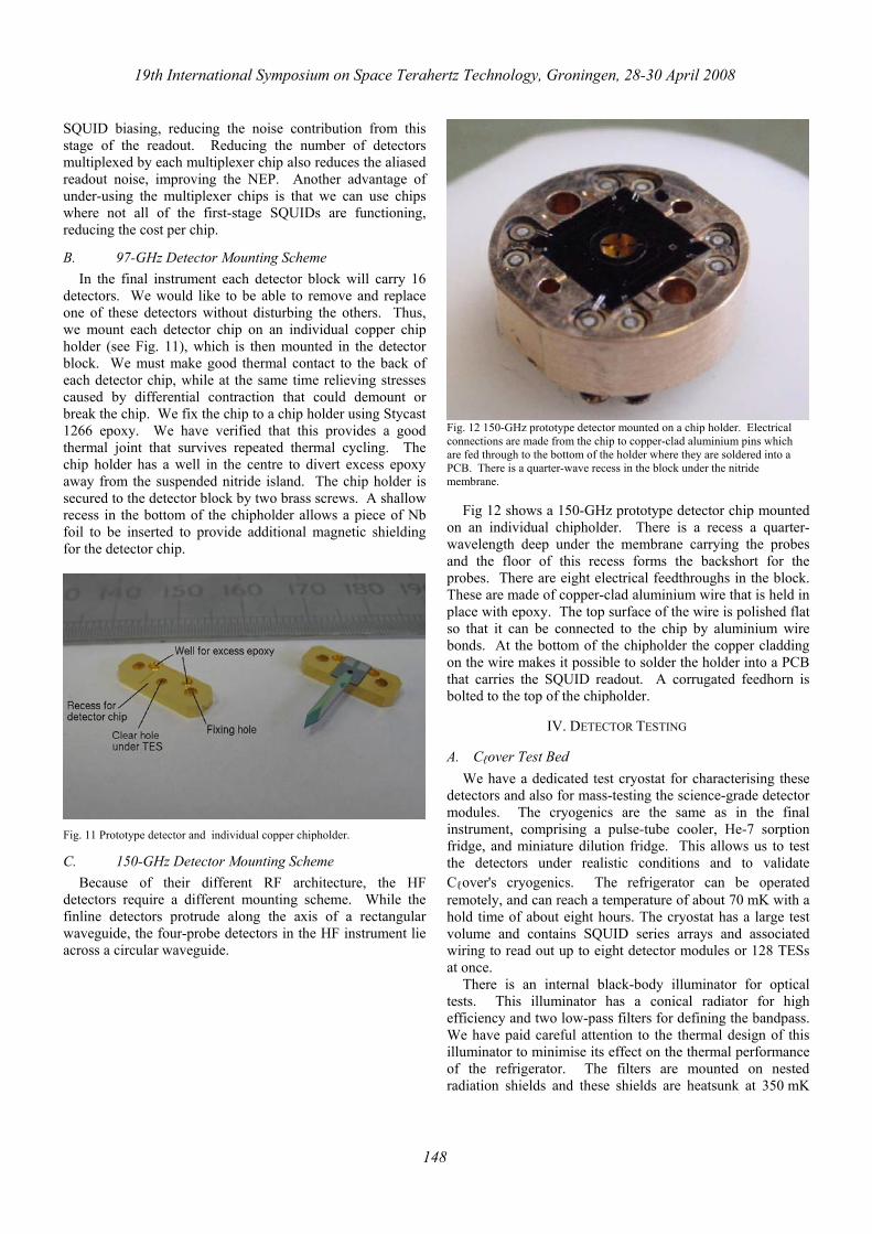
E. 150-GHz Prototype Detectors Fig. shows prototype four-probe OMT detectors that were
fabricated for Cℓover. Fabrication of these chips uses exactly the same process as the 97-GHz finline detectors, except that an extra niobium and an extra insulating layer are needed for the microstrip crossings (see Fig. 8). These crossings are required to allow us to route the microstrips’ signals from opposite pairs of waveguide probes so that they terminate on a single nitride island where the power from both of them is combined and detected by the same TES.
Fig. 6 Prototype 150-GHz Cℓover detector chips fabricated on a 2'' wafer. Each chip is about 6 mm square.
19th International Symposium on Space Terahertz Technology, Groningen, 28-30 April 2008
146
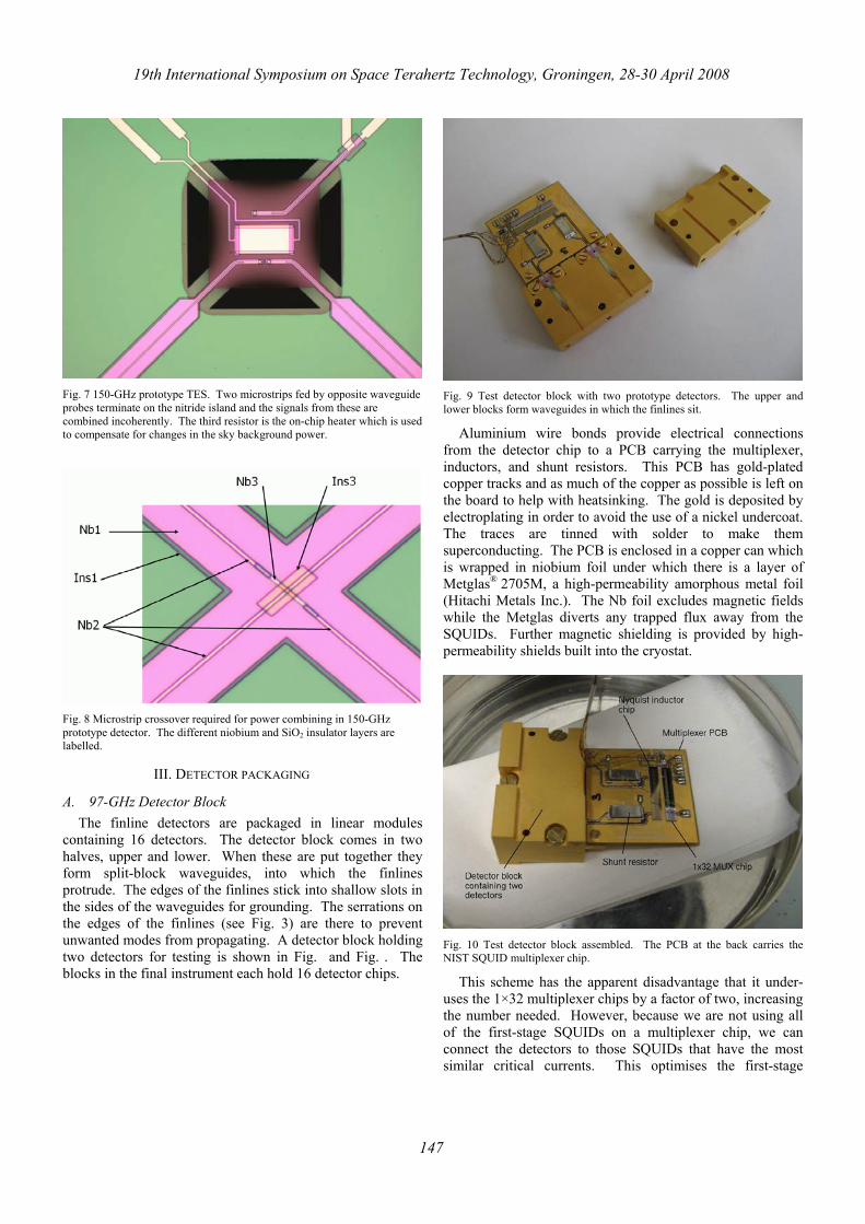
Fig. 7 150-GHz prototype TES. Two microstrips fed by opposite waveguide probes terminate on the nitride island and the signals from these are combined incoherently. The third resistor is the on-chip heater which is used to compensate for changes in the sky background power.
Fig. 8 Microstrip crossover required for power combining in 150-GHz prototype detector. The different niobium and SiO2 insulator layers are labelled.
III. DETECTOR PACKAGING
A. 97-GHz Detector Block The finline detectors are packaged in linear modules
containing 16 detectors. The detector block comes in two halves, upper and lower. When these are put together they form split-block waveguides, into which the finlines protrude. The edges of the finlines stick into shallow slots in the sides of the waveguides for grounding. The serrations on the edges of the finlines (see Fig. 3) are there to prevent unwanted modes from propagating. A detector block holding two detectors for testing is shown in Fig. and Fig. . The blocks in the final instrument each hold 16 detector chips.
Fig. 9 Test detector block with two prototype detectors. The upper and lower blocks form waveguides in which the finlines sit.
Aluminium wire bonds provide electrical connections from the detector chip to a PCB carrying the multiplexer, inductors, and shunt resistors. This PCB has gold-plated copper tracks and as much of the copper as possible is left on the board to help with heatsinking. The gold is deposited by electroplating in order to avoid the use of a nickel undercoat. The traces are tinned with solder to make them superconducting. The PCB is enclosed in a copper can which is wrapped in niobium foil under which there is a layer of Metglas® 2705M, a high-permeability amorphous metal foil (Hitachi Metals Inc.). The Nb foil excludes magnetic fields while the Metglas diverts any trapped flux away from the SQUIDs. Further magnetic shielding is provided by high-permeability shields built into the cryostat.
Fig. 10 Test detector block assembled. The PCB at the back carries the NIST SQUID multiplexer chip.
This scheme has the apparent disadvantage that it under-uses the 1×32 multiplexer chips by a factor of two, increasing the number needed. However, because we are not using all of the first-stage SQUIDs on a multiplexer chip, we can connect the detectors to those SQUIDs that have the most similar critical currents. This optimises the first-stage
19th International Symposium on Space Terahertz Technology, Groningen, 28-30 April 2008
147
SQUID biasing, reducing the noise contribution from this stage of the readout. Reducing the number of detectors multiplexed by each multiplexer chip also reduces the aliased readout noise, improving the NEP. Another advantage of under-using the multiplexer chips is that we can use chips where not all of the first-stage SQUIDs are functioning, reducing the cost per chip.
B. 97-GHz Detector Mounting Scheme In the final instrument each detector block will carry 16
detectors. We would like to be able to remove and replace one of these detectors without disturbing the others. Thus, we mount each detector chip on an individual copper chip holder (see Fig. 11), which is then mounted in the detector block. We must make good thermal contact to the back of each detector chip, while at the same time relieving stresses caused by differential contraction that could demount or break the chip. We fix the chip to a chip holder using Stycast 1266 epoxy. We have verified that this provides a good thermal joint that survives repeated thermal cycling. The chip holder has a well in the centre to divert excess epoxy away from the suspended nitride island. The chip holder is secured to the detector block by two brass screws. A shallow recess in the bottom of the chipholder allows a piece of Nb foil to be inserted to provide additional magnetic shielding for the detector chip.
Fig. 11 Prototype detector and individual copper chipholder.
C. 150-GHz Detector Mounting Scheme Because of their different RF architecture, the HF
detectors require a different mounting scheme. While the finline detectors protrude along the axis of a rectangular waveguide, the four-probe detectors in the HF instrument lie across a circular waveguide.
Fig. 12 150-GHz prototype detector mounted on a chip holder. Electrical connections are made from the chip to copper-clad aluminium pins which are fed through to the bottom of the holder where they are soldered into a PCB. There is a quarter-wave recess in the block under the nitride membrane.
Fig 12 shows a 150-GHz prototype detector chip mounted
on an individual chipholder. There is a recess a quarter-wavelength deep under the membrane carrying the probes and the floor of this recess forms the backshort for the probes. There are eight electrical feedthroughs in the block. These are made of copper-clad aluminium wire that is held in place with epoxy. The top surface of the wire is polished flat so that it can be connected to the chip by aluminium wire bonds. At the bottom of the chipholder the copper cladding on the wire makes it possible to solder the holder into a PCB that carries the SQUID readout. A corrugated feedhorn is bolted to the top of the chipholder.
IV. DETECTOR TESTING
A. Cℓover Test Bed We have a dedicated test cryostat for characterising these
detectors and also for mass-testing the science-grade detector modules. The cryogenics are the same as in the final instrument, comprising a pulse-tube cooler, He-7 sorption fridge, and miniature dilution fridge. This allows us to test the detectors under realistic conditions and to validate Cℓover's cryogenics. The refrigerator can be operated remotely, and can reach a temperature of about 70 mK with a hold time of about eight hours. The cryostat has a large test volume and contains SQUID series arrays and associated wiring to read out up to eight detector modules or 128 TESs at once.
There is an internal black-body illuminator for optical tests. This illuminator has a conical radiator for high efficiency and two low-pass filters for defining the bandpass. We have paid careful attention to the thermal design of this illuminator to minimise its effect on the thermal performance of the refrigerator. The filters are mounted on nested radiation shields and these shields are heatsunk at 350 mK
19th International Symposium on Space Terahertz Technology, Groningen, 28-30 April 2008
148
and 1 K stages of the He-7 sorption fridge. The conical radiator with its G-10 support structure is shown in Fig. . The thermal conductance to the 1-K end piece is controlled by the length of the wires to the heater and thermometer.
Fig. 13 Black-body illuminator with thermal shields and filters removed.
The test bed also has two parallel sets of warm readout electronics (the MCE and an analogue system) so that we can characterise fully the entire readout chain from the detectors up to room temperature. Unlike the MCE, the analogue electronics does not multiplex, but can be switched between three columns and three rows. However, it is more versatile and convenient for characterising the TESs and SQUIDs. For example, it can lock on any of the three SQUID stages, while the MCE is designed to lock on the first-stage SQUID only. All of the results presented here were obtained with the analogue electronics.
B. Dark NEP Our first generation of devices had excess noise, which we
attribute to internal thermal fluctuation noise. To eliminate this excess noise we modified the TES geometry to improve thermalisation. We found that when we added copper fingers extending most of the way across the TES from opposite edges (see Fig 14) the measured noise in the TES was consistent with what we expected from the known Johnson and phonon noise sources [16]. We thus adopted this geometry for the final design.
Fig. 14 TES with copper fingers extending from the normal copper banks for improving thermalisation and reducing excess noise. This TES geometry was adopted for the science-grade 97-GHz detectors.
The prototype detectors were fabricated with a variety of nitride leg geometries in order to find the leg geometry that would give a thermal conductance consistent with the power-handling requirement.
With a conductance that gives us the power handling we need for the 97-GHz detectors we measure a dark NEP of about 1.7×10⁻¹⁷ W/√Hz, although we have measured NEPs as low as 1.5×10⁻¹⁷ W/√Hz on devices with lower conductance. We satisfy the detector NEP requirement comfortably at 97 GHz. Since the LF instrument has the strictest NEP requirement, we will be able to meet the requirement at the other two frequencies. The time constants of all of the prototype detectors were also consistent with the requirements.
C. 97-GHz Optical Testing For optical testing we mounted a pyramidal feedhorn on
the detector block to improve the coupling of the waveguide to the black-body illuminator. 15 shows the effect of optical illumination on the characteristic current-voltage (IV) curve of the TES in a prototype detector. The IV curves are produced by sweeping the TES bias voltage downwards and recording the feedback current in the SQUIDs' flux-locked loop. At high TES bias voltages the TES is in its normal state and we see ohmic behaviour (the straight part of the IV curve). At lower biases the TES is on its superconducting transition. This is the negative-resistance region of the IV curve where the current increases as the bias voltage decreases. As the illuminator temperature is increased, the point at which the TES saturates and goes normal is driven to lower and lower bias voltages. This deficit in the Joule power needed to drive the detector normal shows that optical power is being absorbed by the detector.
Fig. shows the response of a prototype detector to optical power when it is biased at three different TES bias voltages. The response is linear until the incident power exceeds the detector's power handling at that bias voltage and the TES is driven normal. The detection efficiency is estimated to be 89%.
19th International Symposium on Space Terahertz Technology, Groningen, 28-30 April 2008
149
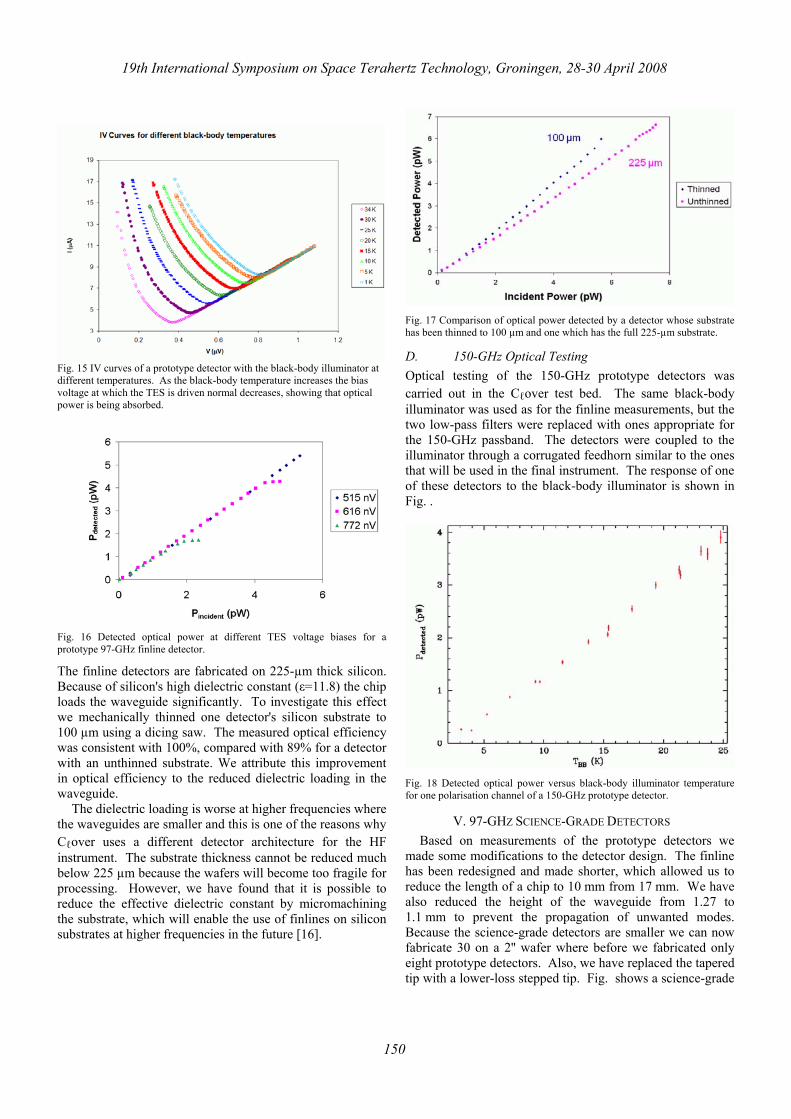
Fig. 15 IV curves of a prototype detector with the black-body illuminator at different temperatures. As the black-body temperature increases the bias voltage at which the TES is driven normal decreases, showing that optical power is being absorbed.
Fig. 16 Detected optical power at different TES voltage biases for a prototype 97-GHz finline detector.
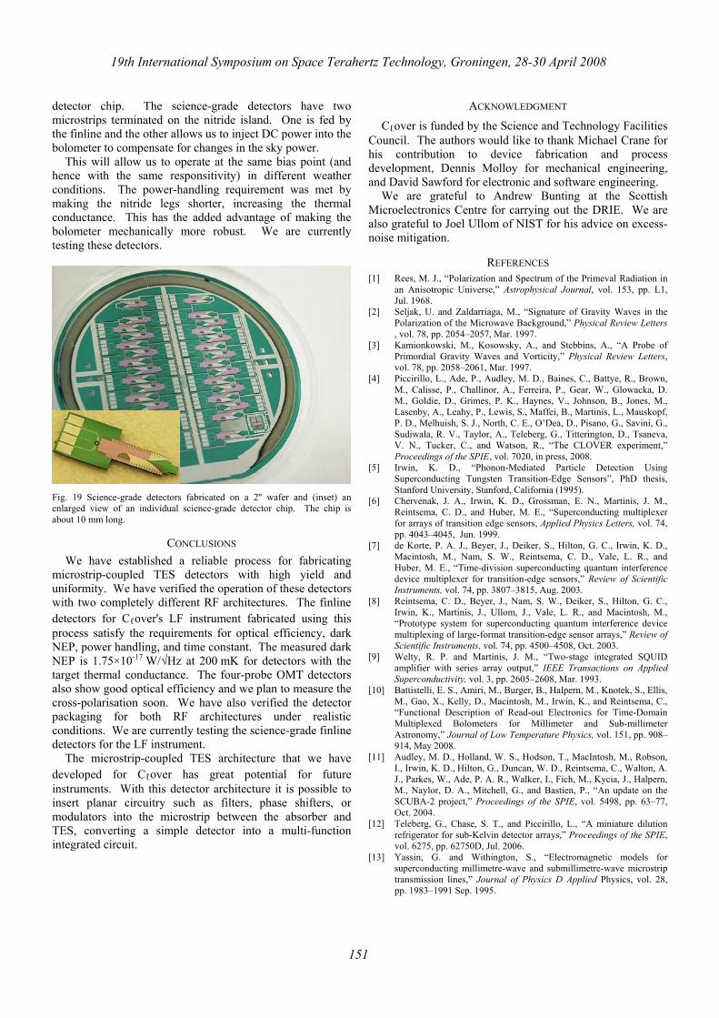
The finline detectors are fabricated on 225-µm thick silicon. Because of silicon's high dielectric constant (ε=11.8) the chip loads the waveguide significantly. To investigate this effect we mechanically thinned one detector's silicon substrate to 100 µm using a dicing saw. The measured optical efficiency was consistent with 100%, compared with 89% for a detector with an unthinned substrate. We attribute this improvement in optical efficiency to the reduced dielectric loading in the waveguide.
The dielectric loading is worse at higher frequencies where the waveguides are smaller and this is one of the reasons why Cℓover uses a different detector architecture for the HF instrument. The substrate thickness cannot be reduced much below 225 µm because the wafers will become too fragile for processing. However, we have found that it is possible to reduce the effective dielectric constant by micromachining the substrate, which will enable the use of finlines on silicon substrates at higher frequencies in the future [16].
Fig. 17 Comparison of optical power detected by a detector whose substrate has been thinned to 100 µm and one which has the full 225-µm substrate.
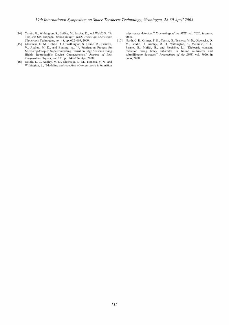
D. 150-GHz Optical Testing Optical testing of the 150-GHz prototype detectors was carried out in the Cℓover test bed. The same black-body illuminator was used as for the finline measurements, but the two low-pass filters were replaced with ones appropriate for the 150-GHz passband. The detectors were coupled to the illuminator through a corrugated feedhorn similar to the ones that will be used in the final instrument. The response of one of these detectors to the black-body illuminator is shown in Fig. .
Fig. 18 Detected optical power versus black-body illuminator temperature for one polarisation channel of a 150-GHz prototype detector.
V. 97-GHZ SCIENCE-GRADE DETECTORS Based on measurements of the prototype detectors we
made some modifications to the detector design. The finline has been redesigned and made shorter, which allowed us to reduce the length of a chip to 10 mm from 17 mm. We have also reduced the height of the waveguide from 1.27 to 1.1 mm to prevent the propagation of unwanted modes. Because the science-grade detectors are smaller we can now fabricate 30 on a 2'' wafer where before we fabricated only eight prototype detectors. Also, we have replaced the tapered tip with a lower-loss stepped tip. Fig. shows a science-grade
19th International Symposium on Space Terahertz Technology, Groningen, 28-30 April 2008
150
detector chip. The science-grade detectors have two microstrips terminated on the nitride island. One is fed by the finline and the other allows us to inject DC power into the bolometer to compensate for changes in the sky power.
This will allow us to operate at the same bias point (and hence with the same responsitivity) in different weather conditions. The power-handling requirement was met by making the nitride legs shorter, increasing the thermal conductance. This has the added advantage of making the bolometer mechanically more robust. We are currently testing these detectors.
Fig. 19 Science-grade detectors fabricated on a 2'' wafer and (inset) an enlarged view of an individual science-grade detector chip. The chip is about 10 mm long.
CONCLUSIONS We have established a reliable process for fabricating
microstrip-coupled TES detectors with high yield and uniformity. We have verified the operation of these detectors with two completely different RF architectures. The finline detectors for Cℓover's LF instrument fabricated using this process satisfy the requirements for optical efficiency, dark NEP, power handling, and time constant. The measured dark NEP is 1.75×10⁻¹⁷ W/√Hz at 200 mK for detectors with the target thermal conductance. The four-probe OMT detectors also show good optical efficiency and we plan to measure the cross-polarisation soon. We have also verified the detector packaging for both RF architectures under realistic conditions. We are currently testing the science-grade finline detectors for the LF instrument.
The microstrip-coupled TES architecture that we have developed for Cℓover has great potential for future instruments. With this detector architecture it is possible to insert planar circuitry such as filters, phase shifters, or modulators into the microstrip between the absorber and TES, converting a simple detector into a multi-function integrated circuit.
ACKNOWLEDGMENT Cℓover is funded by the Science and Technology Facilities
Council. The authors would like to thank Michael Crane for his contribution to device fabrication and process development, Dennis Molloy for mechanical engineering, and David Sawford for electronic and software engineering.
We are grateful to Andrew Bunting at the Scottish Microelectronics Centre for carrying out the DRIE. We are also grateful to Joel Ullom of NIST for his advice on excess-noise mitigation.
REFERENCES [1] Rees, M. J., “Polarization and Spectrum of the Primeval Radiation in
an Anisotropic Universe,” Astrophysical Journal, vol. 153, pp. L1, Jul. 1968.
[2] Seljak, U. and Zaldarriaga, M., “Signature of Gravity Waves in the Polarization of the Microwave Background,” Physical Review Letters , vol. 78, pp. 2054–2057, Mar. 1997.
[3] Kamionkowski, M., Kosowsky, A., and Stebbins, A., “A Probe of Primordial Gravity Waves and Vorticity,” Physical Review Letters, vol. 78, pp. 2058–2061, Mar. 1997.
[4] Piccirillo, L., Ade, P., Audley, M. D., Baines, C., Battye, R., Brown, M., Calisse, P., Challinor, A., Ferreira, P., Gear, W., Glowacka, D. M., Goldie, D., Grimes, P. K., Haynes, V., Johnson, B., Jones, M., Lasenby, A., Leahy, P., Lewis, S., Maffei, B., Martinis, L., Mauskopf, P. D., Melhuish, S. J., North, C. E., O’Dea, D., Pisano, G., Savini, G., Sudiwala, R. V., Taylor, A., Teleberg, G., Titterington, D., Tsaneva, V. N., Tucker, C., and Watson, R., “The CLOVER experiment,” Proceedings of the SPIE, vol. 7020, in press, 2008.
[5] Irwin, K. D., “Phonon-Mediated Particle Detection Using Superconducting Tungsten Transition-Edge Sensors”, PhD thesis, Stanford University, Stanford, California (1995).
[6] Chervenak, J. A., Irwin, K. D., Grossman, E. N., Martinis, J. M., Reintsema, C. D., and Huber, M. E., “Superconducting multiplexer for arrays of transition edge sensors, Applied Physics Letters, vol. 74, pp. 4043–4045, Jun. 1999.
[7] de Korte, P. A. J., Beyer, J., Deiker, S., Hilton, G. C., Irwin, K. D., Macintosh, M., Nam, S. W., Reintsema, C. D., Vale, L. R., and Huber, M. E., “Time-division superconducting quantum interference device multiplexer for transition-edge sensors,” Review of Scientific Instruments, vol. 74, pp. 3807–3815, Aug. 2003.
[8] Reintsema, C. D., Beyer, J., Nam, S. W., Deiker, S., Hilton, G. C., Irwin, K., Martinis, J., Ullom, J., Vale, L. R., and Macintosh, M., “Prototype system for superconducting quantum interference device multiplexing of large-format transition-edge sensor arrays,” Review of Scientific Instruments, vol. 74, pp. 4500–4508, Oct. 2003.
[9] Welty, R. P. and Martinis, J. M., “Two-stage integrated SQUID amplifier with series array output,” IEEE Transactions on Applied Superconductivity, vol. 3, pp. 2605–2608, Mar. 1993.
[10] Battistelli, E. S., Amiri, M., Burger, B., Halpern, M., Knotek, S., Ellis, M., Gao, X., Kelly, D., Macintosh, M., Irwin, K., and Reintsema, C., “Functional Description of Read-out Electronics for Time-Domain Multiplexed Bolometers for Millimeter and Sub-millimeter Astronomy,” Journal of Low Temperature Physics, vol. 151, pp. 908–914, May 2008.
[11] Audley, M. D., Holland, W. S., Hodson, T., MacIntosh, M., Robson, I., Irwin, K. D., Hilton, G., Duncan, W. D., Reintsema, C., Walton, A. J., Parkes, W., Ade, P. A. R., Walker, I., Fich, M., Kycia, J., Halpern, M., Naylor, D. A., Mitchell, G., and Bastien, P., “An update on the SCUBA-2 project,” Proceedings of the SPIE, vol. 5498, pp. 63–77, Oct. 2004.
[12] Teleberg, G., Chase, S. T., and Piccirillo, L., “A miniature dilution refrigerator for sub-Kelvin detector arrays,” Proceedings of the SPIE, vol. 6275, pp. 62750D, Jul. 2006.
[13] Yassin, G. and Withington, S., “Electromagnetic models for superconducting millimetre-wave and submillimetre-wave microstrip transmission lines,” Journal of Physics D Applied Physics, vol. 28, pp. 1983–1991 Sep. 1995.
19th International Symposium on Space Terahertz Technology, Groningen, 28-30 April 2008
151
[14] Yassin, G., Withington, S., Buffey, M., Jacobs, K., and Wulff, S., “A 350-Ghz SIS antipodal finline mixer,” IEEE Trans. on Microwave Theory and Techniques, vol. 48, pp. 662–669, 2000.
[15] Glowacka, D. M., Goldie, D. J., Withington, S., Crane, M., Tsaneva, V., Audley, M. D., and Bunting, A., “A Fabrication Process for Microstrip-Coupled Superconducting Transition Edge Sensors Giving Highly Reproducible Device Characteristics,” Journal of Low Temperature Physics, vol. 151, pp. 249–254, Apr. 2008.
[16] Goldie, D. J., Audley, M. D., Glowacka, D. M., Tsaneva, V. N., and Withington, S., “Modeling and reduction of excess noise in transition
edge sensor detectors,” Proceedings of the SPIE, vol. 7020, in press, 2008.
[17] North, C. E., Grimes, P. K., Yassin, G., Tsaneva, V. N., Glowacka, D. M., Goldie, D., Audley, M. D., Withington, S., Melhuish, S. J., Pisano, G., Maffei, B., and Piccirillo, L., “Dielectric constant reduction using holey substrates in finline millimeter and submillimeter detectors,” Proceedings of the SPIE, vol. 7020, in press, 2008.
19th International Symposium on Space Terahertz Technology, Groningen, 28-30 April 2008
152