Embed Size (px)
Citation preview
4900180-001.A00 Page 1 of 24
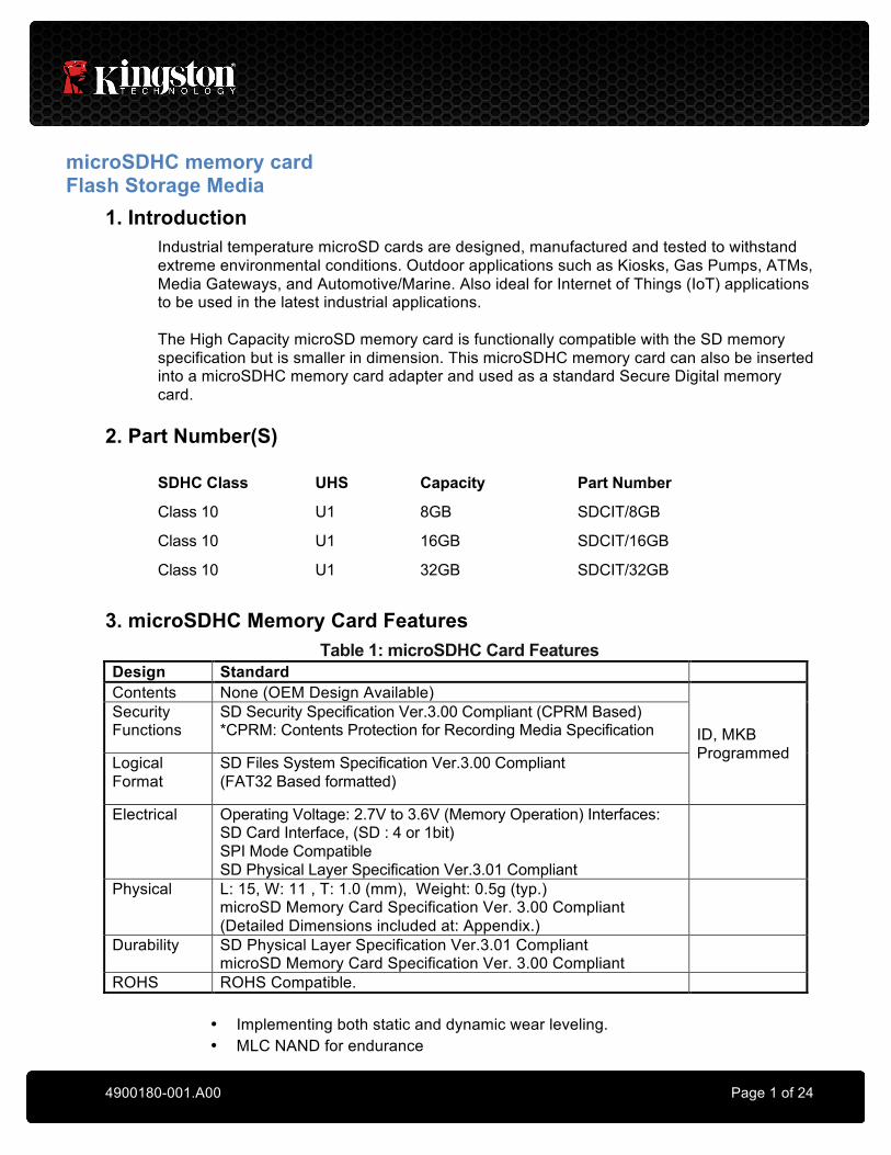
microSDHC memory card Flash Storage Media
1. Introduction Industrial temperature microSD cards are designed, manufactured and tested to withstand extreme environmental conditions. Outdoor applications such as Kiosks, Gas Pumps, ATMs, Media Gateways, and Automotive/Marine. Also ideal for Internet of Things (IoT) applications to be used in the latest industrial applications. The High Capacity microSD memory card is functionally compatible with the SD memory specification but is smaller in dimension. This microSDHC memory card can also be inserted into a microSDHC memory card adapter and used as a standard Secure Digital memory card.
2. Part Number(S)
SDHC Class UHS Capacity Part Number
Class 10 U1 8GB SDCIT/8GB
Class 10 U1 16GB SDCIT/16GB
Class 10 U1 32GB SDCIT/32GB
3. microSDHC Memory Card Features Table 1: microSDHC Card Features
Design Standard Contents None (OEM Design Available)
ID, MKB Programmed
Security Functions
SD Security Specification Ver.3.00 Compliant (CPRM Based) *CPRM: Contents Protection for Recording Media Specification
Logical Format
SD Files System Specification Ver.3.00 Compliant (FAT32 Based formatted)
Electrical Operating Voltage: 2.7V to 3.6V (Memory Operation) Interfaces: SD Card Interface, (SD : 4 or 1bit) SPI Mode Compatible SD Physical Layer Specification Ver.3.01 Compliant
Physical L: 15, W: 11 , T: 1.0 (mm), Weight: 0.5g (typ.) microSD Memory Card Specification Ver. 3.00 Compliant (Detailed Dimensions included at: Appendix.)
Durability SD Physical Layer Specification Ver.3.01 Compliant microSD Memory Card Specification Ver. 3.00 Compliant
ROHS ROHS Compatible.
• Implementing both static and dynamic wear leveling. • MLC NAND for endurance
4900180-001.A00 Page 2 of 24
4. Compatibility
Compliant Specifications SD Memory Card Specifications
• Compliant with PHYSICAL LAYER SPECIFICATION Ver.3.01. (Part1) • Compliant with FILE SYSTEM SPECIFICATION Ver.3.00. (Part2) • Compliant with SECURITY SPECIFICATION Ver.3.00. (Part3) • microSD Memory Card Specification Ver. 3.00
5. Physical Characteristics 5.1. Temperature
1) Operation Conditions Temperature Range: Ta = -40°C to +85°C 2) Storage Conditions Temperature Range: Tstg = -40°C to +85°C
5.2. Moisture (Reliability)
1) Operation Conditions Temperature 25°C / 95% rel. humidity 2) Storage Conditions Temperature 40°C / 95% rel. humidity / 500h
5.3. Application
1) Hot Insertion or Removal
a. Kingston microSDHC Memory Card can be removed and/or inserted without powering off the host system.
2) Mechanical Write Protect Switch
a. microSDHC Memory Card has no mechanical write protect switch.
5.4 Configuration Controller: PS8210DF NAND: Toshiba 15nm MLC 64Gb
4900180-001.A00 Page 3 of 24
6. Electrical Interface Outlines
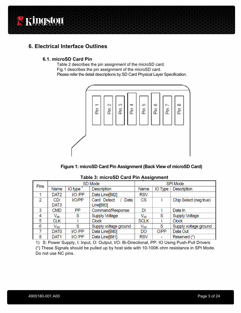
6.1. microSD Card Pin Table 2 describes the pin assignment of the microSD card. Fig.1 describes the pin assignment of the microSD card. Please refer the detail descriptions by SD Card Physical Layer Specification.
Figure 1: microSD Card Pin Assignment (Back View of microSD Card)
Table 3: microSD Card Pin Assignment
1) S: Power Supply, I: Input, O: Output, I/O: Bi-Directional, PP: IO Using Push-Pull Drivers (*) These Signals should be pulled up by host side with 10-100K ohm resistance in SPI Mode. Do not use NC pins.
4900180-001.A00 Page 4 of 24
6.2. microSD Card Bus Topology
The microSD Memory Card supports two alternative communication protocols: SD and SPI Bus Mode. Host System can choose either one of modes. Same Data of the microSD Card can read and write by both modes. SD Mode allows the 4-bit high performance data transfer. SPI Mode allows easy and common interface for SPI channel. The disadvantage of this mode is loss of performance, relatively to the SD mode.
6.2.1. SD Bus Mode Protocol The SD bus allows the dynamic configuration of the number of data line from 1 to 4 Bi-directional data signal. After power up by default, the microSD card will use only DAT0. After initialization, host can change the bus width. Multiplied microSD cards connections are available to the host. Common Vdd, Vss and CLK signal connections are available in the multiple connection. However, Command, Respond and Data lined (DAT0-DAT3) shall be divided for each card from host. This feature allows easy trade-off between hardware cost and system performance. Communication over the microSD bus is based on command and data bit stream initiated by a start bit and terminated by stop bit. Command: Commands are transferred serially on the CMD line. A command is a token to starts an operation from host to the card. Commands are sent to a addressed single card(addressed Command) or to all connected cards (Broad cast command). Response: Responses are transferred serially on the CMD line. A response is a token to answer to a previous received command. Responses are sent from a addressed single card or from all connected cards. Data: Data can be transfer from the card to the host or vice versa. Data is transferred via the data lines.
4900180-001.A00 Page 5 of 24
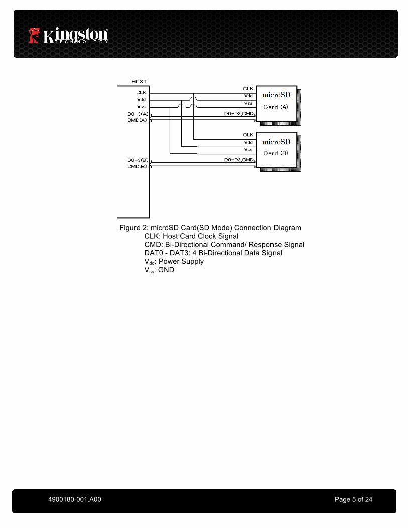
Figure 2: microSD Card(SD Mode) Connection Diagram
CLK: Host Card Clock Signal CMD: Bi-Directional Command/ Response Signal DAT0 - DAT3: 4 Bi-Directional Data Signal Vdd: Power Supply Vss: GND
4900180-001.A00 Page 6 of 24
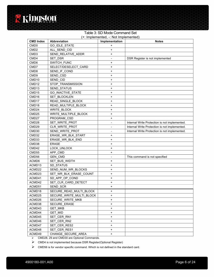
Table 3: SD Mode Command Set (+: Implemented, -: Not Implemented)
CMD Index Abbreviation Implementation Notes CMD0 GO_IDLE_STATE + CMD2 ALL_SEND_CID + CMD3 SEND_RELATIVE_ADDR + CMD4 SET_DSR - DSR Register is not implemented CMD6 SWITCH_FUNC + CMD7 SELECT/DESELECT_CARD + CMD8 SEND_IF_COND + CMD9 SEND_CSD + CMD10 SEND_CID + CMD12 STOP_TRANSMISSION + CMD13 SEND_STATUS + CMD15 GO_INACTIVE_STATE + CMD16 SET_BLOCKLEN + CMD17 READ_SINGLE_BLOCK + CMD18 READ_MULTIPLE_BLOCK + CMD24 WRITE_BLOCK + CMD25 WRITE_MULTIPLE_BLOCK + CMD27 PROGRAM_CSD + CMD28 SET_WRITE_PROT - Internal Write Protection is not implemented. CMD29 CLR_WRITE_PROT - Internal Write Protection is not implemented. CMD30 SEND_WRITE_PROT - Internal Write Protection is not implemented. CMD32 ERASE_WR_BLK_START + CMD33 ERASE_WR_BLK_END + CMD38 ERASE + CMD42 LOCK_UNLOCK + CMD55 APP_CMD + CMD56 GEN_CMD - This command is not specified ACMD6 SET_BUS_WIDTH + ACMD13 SD_STATUS + ACMD22 SEND_NUM_WR_BLOCKS + ACMD23 SET_WR_BLK_ERASE_COUNT + ACMD41 SD_APP_OP_COND + ACMD42 SET_CLR_CARD_DETECT + ACMD51 SEND_SCR + ACMD18 SECURE_READ_MULTI_BLOCK + ACMD25 SECURE_WRITE_MULTI_BLOCK + ACMD26 SECURE_WRITE_MKB + ACMD38 SECURE_ERASE + ACMD43 GET_MKB + ACMD44 GET_MID + ACMD45 SET_CER_RN1 + ACMD46 SET_CER_RN2 + ACMD47 SET_CER_RES2 + ACMD48 SET_CER_RES1 + ACMD49 CHANGE_SECURE_AREA + Ø CMD28, 29 and CMD30 are Optional Commands. Ø CMD4 is not implemented because DSR Register(Optional Register) Ø CMD56 is for vendor specific command. Which is not defined in the standard card.
4900180-001.A00 Page 7 of 24
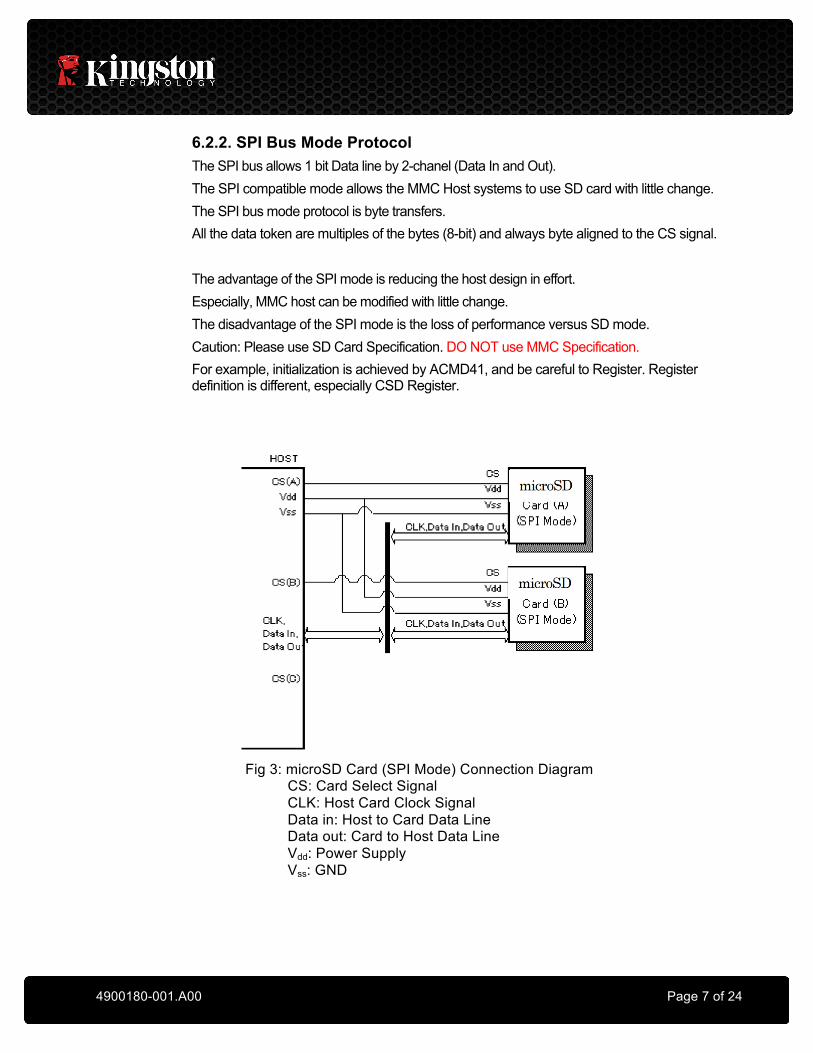
6.2.2. SPI Bus Mode Protocol The SPI bus allows 1 bit Data line by 2-chanel (Data In and Out). The SPI compatible mode allows the MMC Host systems to use SD card with little change. The SPI bus mode protocol is byte transfers. All the data token are multiples of the bytes (8-bit) and always byte aligned to the CS signal. The advantage of the SPI mode is reducing the host design in effort. Especially, MMC host can be modified with little change. The disadvantage of the SPI mode is the loss of performance versus SD mode. Caution: Please use SD Card Specification. DO NOT use MMC Specification. For example, initialization is achieved by ACMD41, and be careful to Register. Register definition is different, especially CSD Register.
Fig 3: microSD Card (SPI Mode) Connection Diagram
CS: Card Select Signal CLK: Host Card Clock Signal Data in: Host to Card Data Line Data out: Card to Host Data Line Vdd: Power Supply Vss: GND
4900180-001.A00 Page 8 of 24
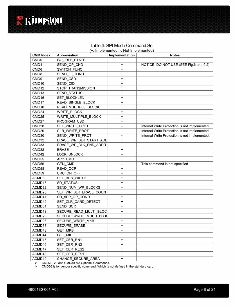
Table.4: SPI Mode Command Set (+: Implemented, -: Not Implemented)
CMD Index Abbreviation Implementation Notes CMD0 GO_IDLE_STATE + CMD1 SEND_OP_CND + NOTICE: DO NOT USE (SEE Fig.6 and 9.2) CMD6 SWITCH_FUNC + CMD8 SEND_IF_COND + CMD9 SEND_CSD + CMD10 SEND_CID + CMD12 STOP_TRANSMISSION + CMD13 SEND_STATUS + CMD16 SET_BLOCKLEN + CMD17 READ_SINGLE_BLOCK + CMD18 READ_MULTIPLE_BLOCK + CMD24 WRITE_BLOCK + CMD25 WRITE_MULTIPLE_BLOCK + CMD27 PROGRAM_CSD + CMD28 SET_WRITE_PROT - Internal Write Protection is not implemented. CMD29 CLR_WRITE_PROT - Internal Write Protection is not implemented. CMD30 SEND_WRITE_PROT - Internal Write Protection is not implemented. CMD32 ERASE_WR_BLK_START_ADDR + CMD33 ERASE_WR_BLK_END_ADDR + CMD38 ERASE + CMD42 LOCK_UNLOCK + CMD55 APP_CMD + CMD56 GEN_CMD - This command is not specified CMD58 READ_OCR + CMD59 CRC_ON_OFF + ACMD6 SET_BUS_WIDTH + ACMD13 SD_STATUS + ACMD22 SEND_NUM_WR_BLOCKS + ACMD23 SET_WR_BLK_ERASE_COUNT + ACMD41 SD_APP_OP_COND + ACMD42 SET_CLR_CARD_DETECT + ACMD51 SEND_SCR + ACMD18 SECURE_READ_MULTI_BLOCK + ACMD25 SECURE_WRITE_MULTI_BLOCK + ACMD26 SECURE_WRITE_MKB + ACMD38 SECURE_ERASE + ACMD43 GET_MKB + ACMD44 GET_MID + ACMD45 SET_CER_RN1 + ACMD46 SET_CER_RN2 + ACMD47 SET_CER_RES2 + ACMD48 SET_CER_RES1 + ACMD49 CHANGE_SECURE_AREA + Ø CMD28, 29 and CMD30 are Optional Commands. Ø CMD56 is for vendor specific command. Which is not defined in the standard card.
4900180-001.A00 Page 9 of 24
6.3. microSD Card Initialize
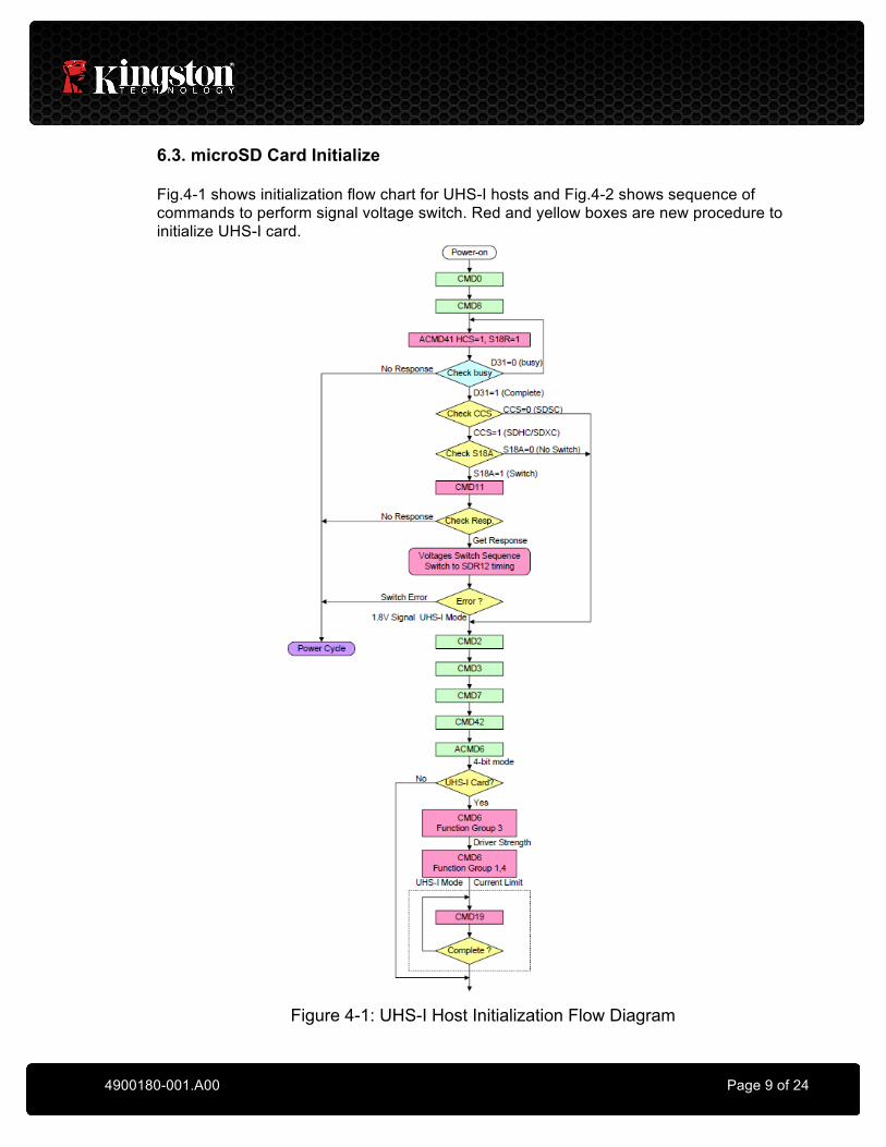
Fig.4-1 shows initialization flow chart for UHS-I hosts and Fig.4-2 shows sequence of commands to perform signal voltage switch. Red and yellow boxes are new procedure to initialize UHS-I card.
Figure 4-1: UHS-I Host Initialization Flow Diagram
4900180-001.A00 Page 10 of 24
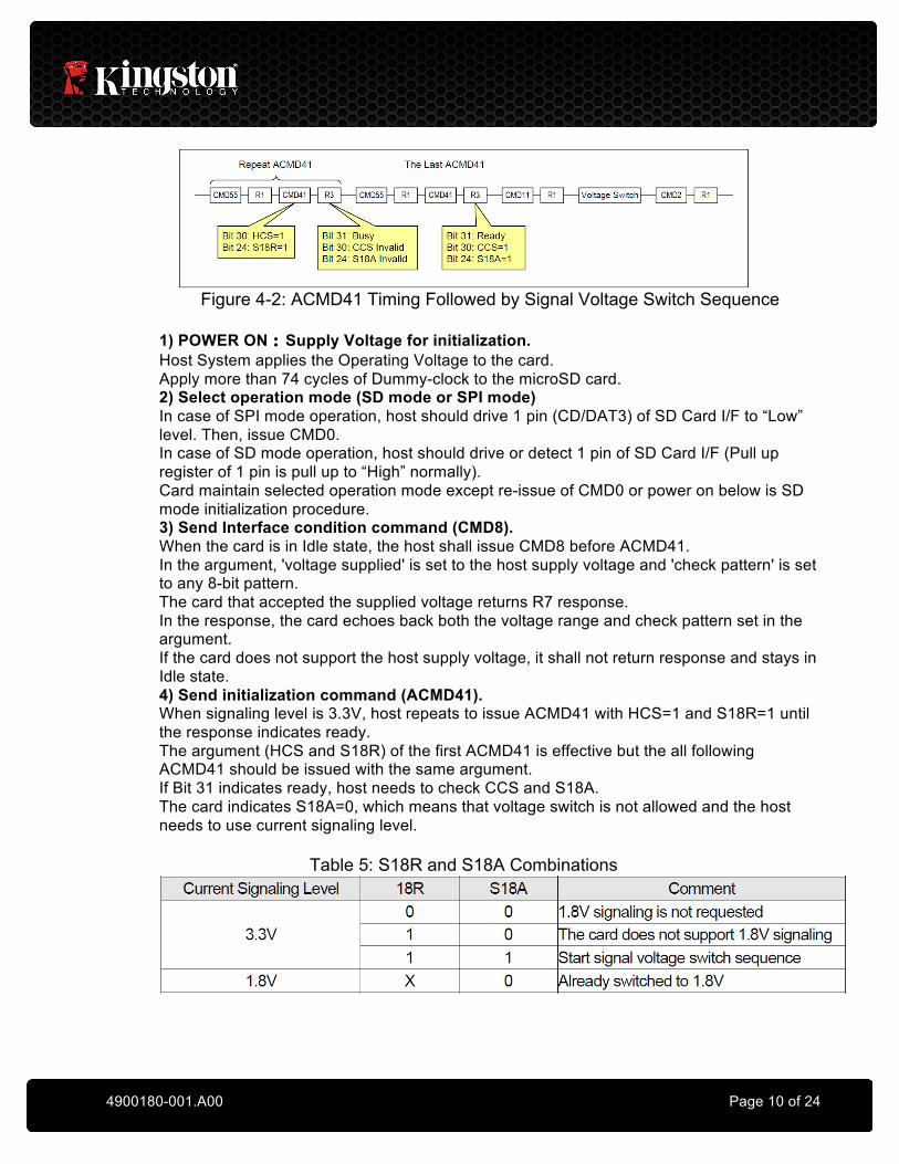
Figure 4-2: ACMD41 Timing Followed by Signal Voltage Switch Sequence
1) POWER ON:Supply Voltage for initialization. Host System applies the Operating Voltage to the card. Apply more than 74 cycles of Dummy-clock to the microSD card. 2) Select operation mode (SD mode or SPI mode) In case of SPI mode operation, host should drive 1 pin (CD/DAT3) of SD Card I/F to “Low” level. Then, issue CMD0. In case of SD mode operation, host should drive or detect 1 pin of SD Card I/F (Pull up register of 1 pin is pull up to “High” normally). Card maintain selected operation mode except re-issue of CMD0 or power on below is SD mode initialization procedure. 3) Send Interface condition command (CMD8). When the card is in Idle state, the host shall issue CMD8 before ACMD41. In the argument, 'voltage supplied' is set to the host supply voltage and 'check pattern' is set to any 8-bit pattern. The card that accepted the supplied voltage returns R7 response. In the response, the card echoes back both the voltage range and check pattern set in the argument. If the card does not support the host supply voltage, it shall not return response and stays in Idle state. 4) Send initialization command (ACMD41). When signaling level is 3.3V, host repeats to issue ACMD41 with HCS=1 and S18R=1 until the response indicates ready. The argument (HCS and S18R) of the first ACMD41 is effective but the all following ACMD41 should be issued with the same argument. If Bit 31 indicates ready, host needs to check CCS and S18A. The card indicates S18A=0, which means that voltage switch is not allowed and the host needs to use current signaling level.
Table 5: S18R and S18A Combinations
4900180-001.A00 Page 11 of 24
5) Send voltage switch command (CMD11). S18A=1 means that voltage switch is allowed and host issues CMD11 to invoke voltage switch sequence. By receiving CMD11, the card returns R1 response and start voltage switch sequence. No response of CMD11 means that S18A was 0 and therefore host should not have sent CMD11. Completion of voltage switch sequence is checked by high level of DAT[3:0]. Any bit of DAT[3:0] can be checked depends on ability of the host. The card enters UHS-I mode and card input and output timings are changed (SDR12 in default) when the voltage switch sequence is completed successfully. 6) Send ALL_SEND_CID command (CMD2) and get the Card ID (CID). 7) Send SEND_RELATIVE_ADDR (CMD3) and get the RCA. RCA value is randomly changed by access, not equal zero. 8) Send SELECT / DESELECT_CARD command (CMD7) and move to the transfer state. When entering tran state, CARD_IS_LOCKED status in the R1 response should be checked (it is indicated in the response of CMD7). If the CARD_IS_LOCKED status is set to 1 in the response of CMD7, CMD42 is required before ACMD6 to unlock the card. ( If the card is locked, CMD42 is required to unlock the card. ) If the card is unlocked, CMD42 can be skipped. 9) Send SET_BUS_WIDTH command (ACMD6). UHS-I supports only 4-bit mode. Host shall select 4-bit mode by ACMD6. If the card is locked, host needs to unlock the card by CMD42 in 1-bit mode and then needs to issue ACMD6 to change 4-bit bus mode. Operating in 1-bit mode is not assured. 10) Set driver strength. CMD6 mode 0 is used to query which functions the card supports, and to identify the maximum current consumption of the card under the selected functions. In case of UHS-I card, appropriate driver strength (default is Type-B buffer) is selected by CMD6 Function Group 3. 11) Set UHS-I mode current limit. UHS-I modes ( Bus Speed Mode ) is selected by CMD6 Function Group 1. Current Limit is selected by CMD6 Function Group 4. Maximum access settings: SDR50 = (CMD6 Function Group 1 = 2-h, CMD6 Function Group 4 = 1-h)
Note: Function Group 4 is defined as Current Limit switch for SDR50. The Current Limit does not act on the card in SDR12 and SDR25. The default value of the Current Limit is 200mA (minimum setting). Then after selecting one of SDR50 mode by Function Group 1, host needs to change the Current Limit to enable the card to operate in higher performance. This value is determined by a host power supply capability to the card, heat release method taken by a host and the maximum current of a connector. 12) Tuning of sampling point CMD19 sends a tuning block to the host to determine sampling point. In SDR50 and SDR104 modes, if tuning of sampling point is required, CMD19 is repeatedly issued until tuning is completed Then the Host can access the Data between the SD card as a storage device.
4900180-001.A00 Page 12 of 24
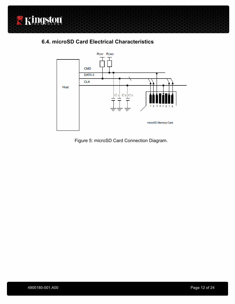
6.4. microSD Card Electrical Characteristics
Figure 5: microSD Card Connection Diagram.
4900180-001.A00 Page 13 of 24
6.4.1. DC Characteristics
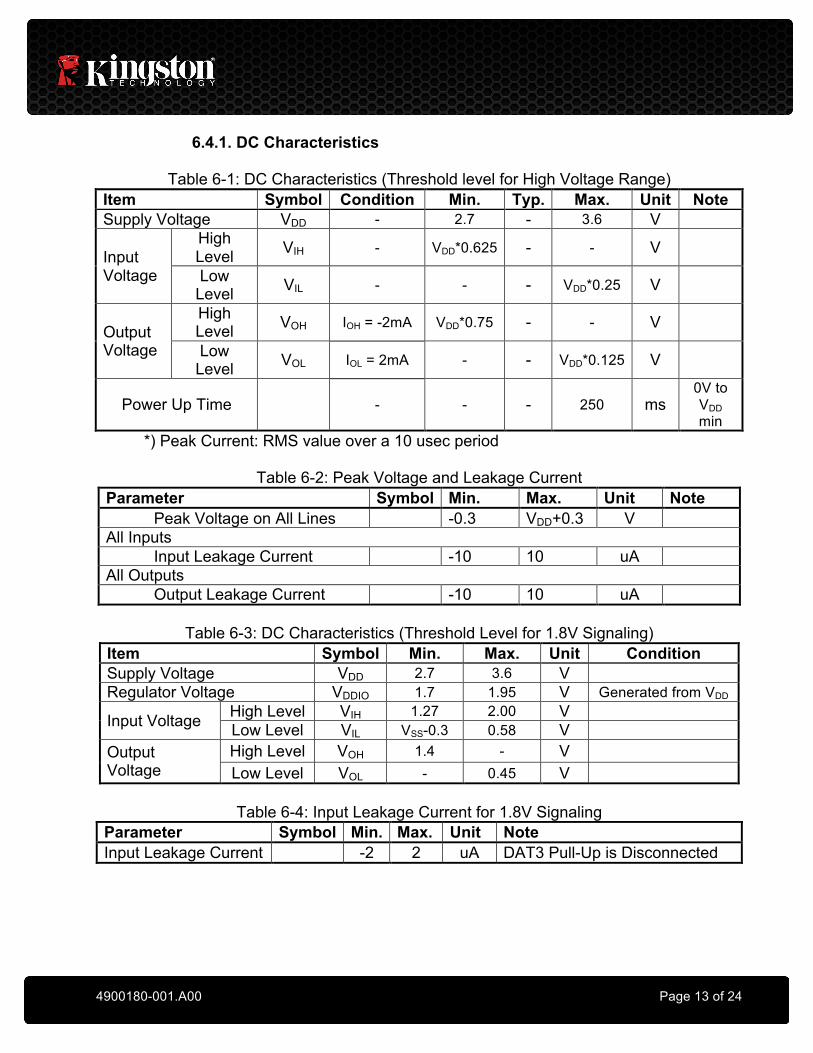
Table 6-1: DC Characteristics (Threshold level for High Voltage Range)
Item Symbol Condition Min. Typ. Max. Unit Note Supply Voltage VDD - 2.7 - 3.6 V
Input Voltage
High Level VIH - VDD*0.625 - - V Low
Level VIL - - - VDD*0.25 V
Output Voltage
High Level VOH IOH = -2mA VDD*0.75 - - V Low
Level VOL IOL = 2mA - - VDD*0.125 V
Power Up Time - - - 250 ms 0V to VDD min
*) Peak Current: RMS value over a 10 usec period
Table 6-2: Peak Voltage and Leakage Current Parameter Symbol Min. Max. Unit Note
Peak Voltage on All Lines -0.3 VDD+0.3 V All Inputs
Input Leakage Current -10 10 uA All Outputs
Output Leakage Current -10 10 uA
Table 6-3: DC Characteristics (Threshold Level for 1.8V Signaling) Item Symbol Min. Max. Unit Condition Supply Voltage VDD 2.7 3.6 V Regulator Voltage VDDIO 1.7 1.95 V Generated from VDD
Input Voltage High Level VIH 1.27 2.00 V Low Level VIL VSS-0.3 0.58 V
Output Voltage
High Level VOH 1.4 - V Low Level VOL - 0.45 V
Table 6-4: Input Leakage Current for 1.8V Signaling
Parameter Symbol Min. Max. Unit Note Input Leakage Current -2 2 uA DAT3 Pull-Up is Disconnected
4900180-001.A00 Page 14 of 24
Table 6-5: Power Consumption
Item Symbol
Condition Min. Typ. Max. Unit Note
Standby Current ICCS 3.0V Clock Stop - - 950 uA @ 25°C
Operation Current(Peak)
ICCOP1 *1)
Current Limit=400mA VDD=3.6V
- - 300
mA @ 25°C
Current Limit=200mA VDD=3.6V
- - 300
(HS or DS) VDD=3.6V
- - 300
Operation Current(Average)
ICCOP2 *2)
Current Limit=400mA VDD=3.6V
- - 250
mA @ 25°C
Current Limit=200mA VDD=3.6V
- - 200
(SDR25 or HS) VDD=3.6V
- - 200
(SDR12.5 or DS) VDD=3.6V
- - 100
*1) Peak Current: RMS value over a 10usec period *2) Average Current: value over 1 sec period.
Table 6-6: Signal Capacitance Total Bus Capacitance = CHOST + CBUS + N*CCard Item Symbol Min. Max. Unit Note
Pull-Up Resistance RCMD RDAT 10 100 K Ohm
Total Bus Capacitance for Each Signal Line CL - 40 pF
1 Card CHOST+CBUS Shall Not Exceed 30pF
Card Capacitance for Each Signal Pin CCARD - 10 pF
Maximum Signal Line Inductance - 16 nH
Pull-Up Resistance Inside Card(Pin 1) RDAT3 10 90 K Ohm
May Be Used for Card
Detection
Capacity Connected to Power Line CC - 5 uF To Prevent Inrush Current
Note: WP pull-up (Rwp) Value is depend on the Host Interface drive circuit.
4900180-001.A00 Page 15 of 24
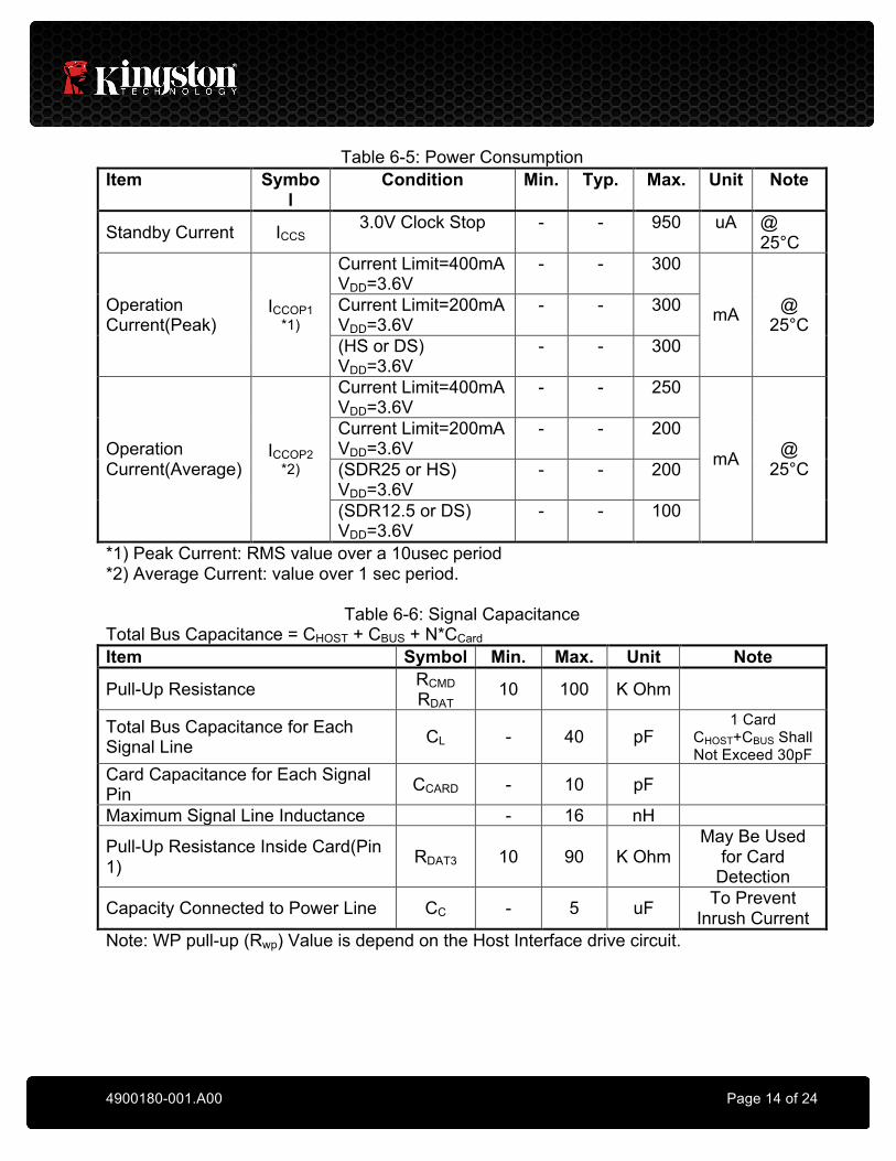
6.4.2. AC Characteristics (Default)
Figure 6-1: AC Timing Diagram (Default)
Table 7-1: AC Characteristics (Default)
Item Symbol Min. Max. Unit Note Clock Frequency (In Any State) fSTP 0 25 MHz
CCARD ≤ 10pF (1 Card)
Clock Frequency (Data Transfer Mode) fPP 0 25 MHz
Clock Frequency (Card Identification Mode) fOD 0/100(*1) 400 KHz
Clock Low Time tWL 10 - ns Clock High Time tWH 10 - ns Clock Rise Time tTLH - 10 ns Clock Fall Time tTHL - 10 ns Input Set-up Time tISU 5 - ns Input Hold Time tIH 5 - ns Output Delay Time (Data Transfer Mode) tODLY 0 14 ns CL ≤ 40pF
(1 Card) Output Delay Time (Identification Mode) tODLY 0 50 ns
(*1) 0Hz means to stop the clock. The given minimum frequency range is for cases were continues clock is required.
4900180-001.A00 Page 16 of 24
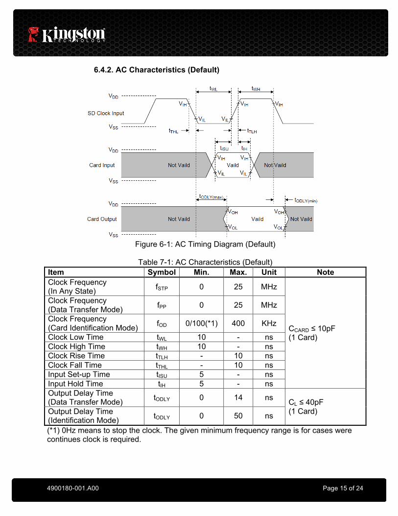
6.4.3. AC Characteristics (High-Speed)
Figure 6-2: AC Timing Diagram (High-Speed)
Table 7-2: AC Characteristics (High-Speed) Item Symbol Min. Max. Unit Note Clock Frequency (Data Transfer Mode) fPP 0 50 MHz CCARD ≤ 10pF (1 Card)
Clock Low Time tWL 7 - ns CCARD ≤ 10pF (1 Card) Clock High Time tWH 7 - ns CCARD ≤ 10pF (1 Card) Clock Rise Time tTLH - 3 ns CCARD ≤ 10pF (1 Card) Clock Fall Time tTHL - 3 ns CCARD ≤ 10pF (1 Card) Input Set-up Time tISU 6 - ns CCARD ≤ 10pF (1 Card) Input Hold Time tIH 2 - ns CCARD ≤ 10pF (1 Card) Output Delay Time (Data Transfer Mode) tODLY - 14 ns CCARD ≤ 10pF (1 Card)
Output Hold Time TOH 2.5 - ns CCARD ≤ 10pF (1 Card) Total System Capacitance CL - 40 pF CCARD≤10pF (1 Card)
4900180-001.A00 Page 17 of 24
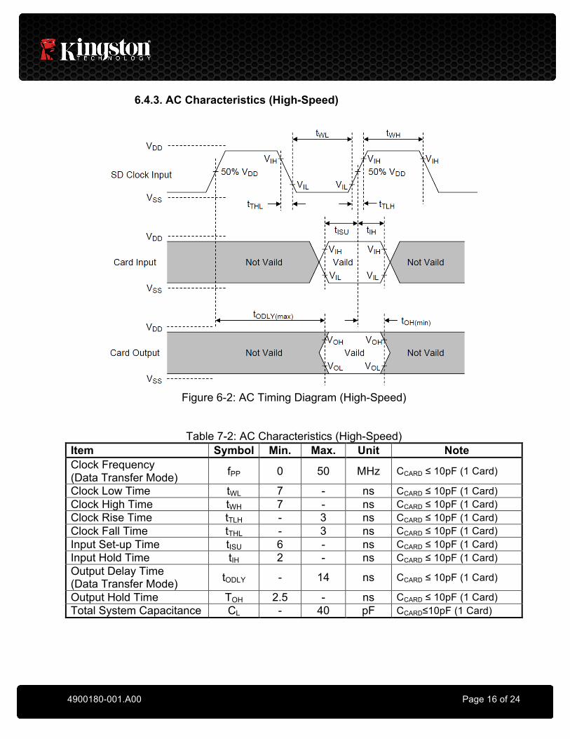
6.4.4 AC Characteristics (SDR12, SDR25, SDR50, and SDR104 Modes)
Figure 6-3: AC Timing Diagram (SDR12, SDR25, SDR50, and SDR104 Modes Input)
Table 7-3: AC Characteristics (SDR12, SDR25, SDR50, and SDR104 Modes Input)
Symbol Min. Max. Unit Remark tCLK 4.80 - ns 208MHz(Max.), between rising edge,
VCT=0.975V tCR, tCF - 0.2*tCLK ns tCR, tCF < 2.00ns(Max.) at 100MHz, CCARD =
10pF Clock Duty
30 70 %
4900180-001.A00 Page 18 of 24
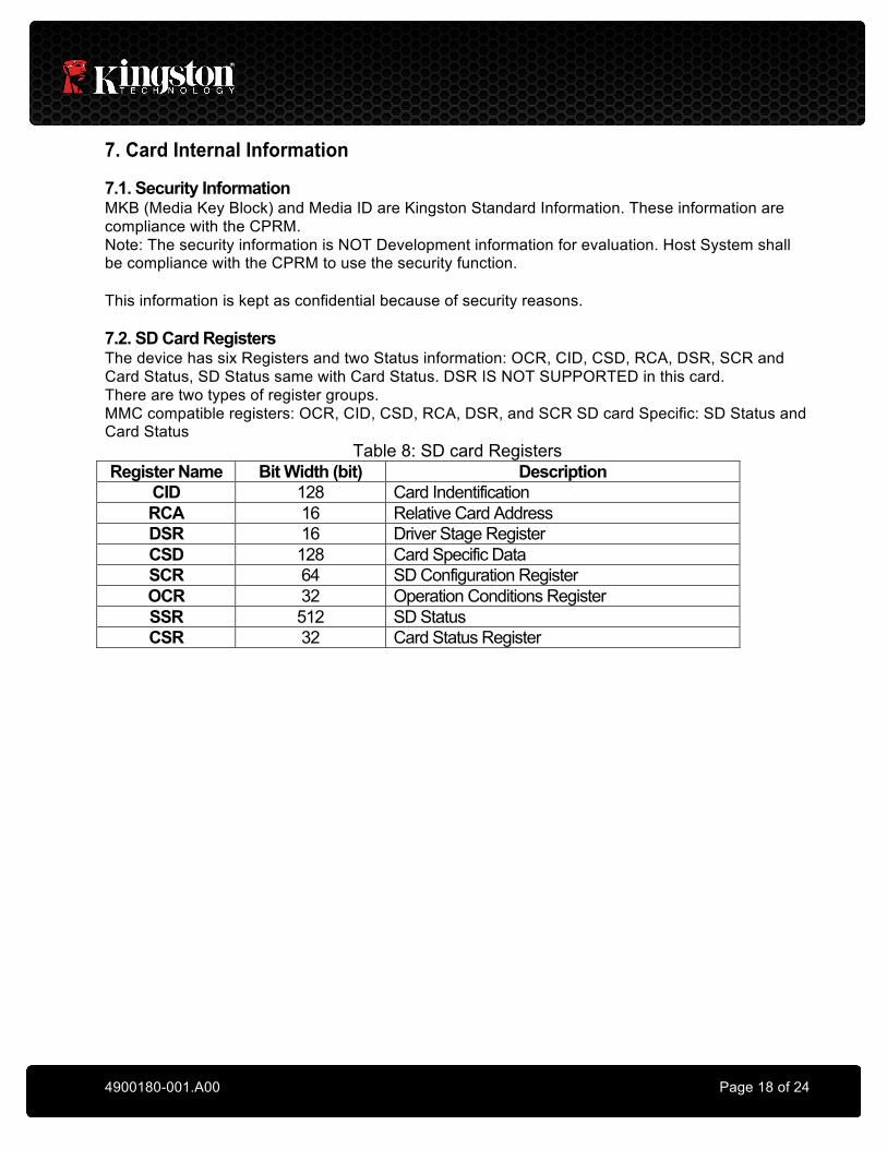
7. Card Internal Information
7.1. Security Information MKB (Media Key Block) and Media ID are Kingston Standard Information. These information are compliance with the CPRM. Note: The security information is NOT Development information for evaluation. Host System shall be compliance with the CPRM to use the security function.
This information is kept as confidential because of security reasons.
7.2. SD Card Registers The device has six Registers and two Status information: OCR, CID, CSD, RCA, DSR, SCR and Card Status, SD Status same with Card Status. DSR IS NOT SUPPORTED in this card. There are two types of register groups. MMC compatible registers: OCR, CID, CSD, RCA, DSR, and SCR SD card Specific: SD Status and Card Status
Table 8: SD card Registers Register Name Bit Width (bit) Description
CID 128 Card Indentification RCA 16 Relative Card Address DSR 16 Driver Stage Register CSD 128 Card Specific Data SCR 64 SD Configuration Register OCR 32 Operation Conditions Register SSR 512 SD Status CSR 32 Card Status Register
4900180-001.A00 Page 19 of 24
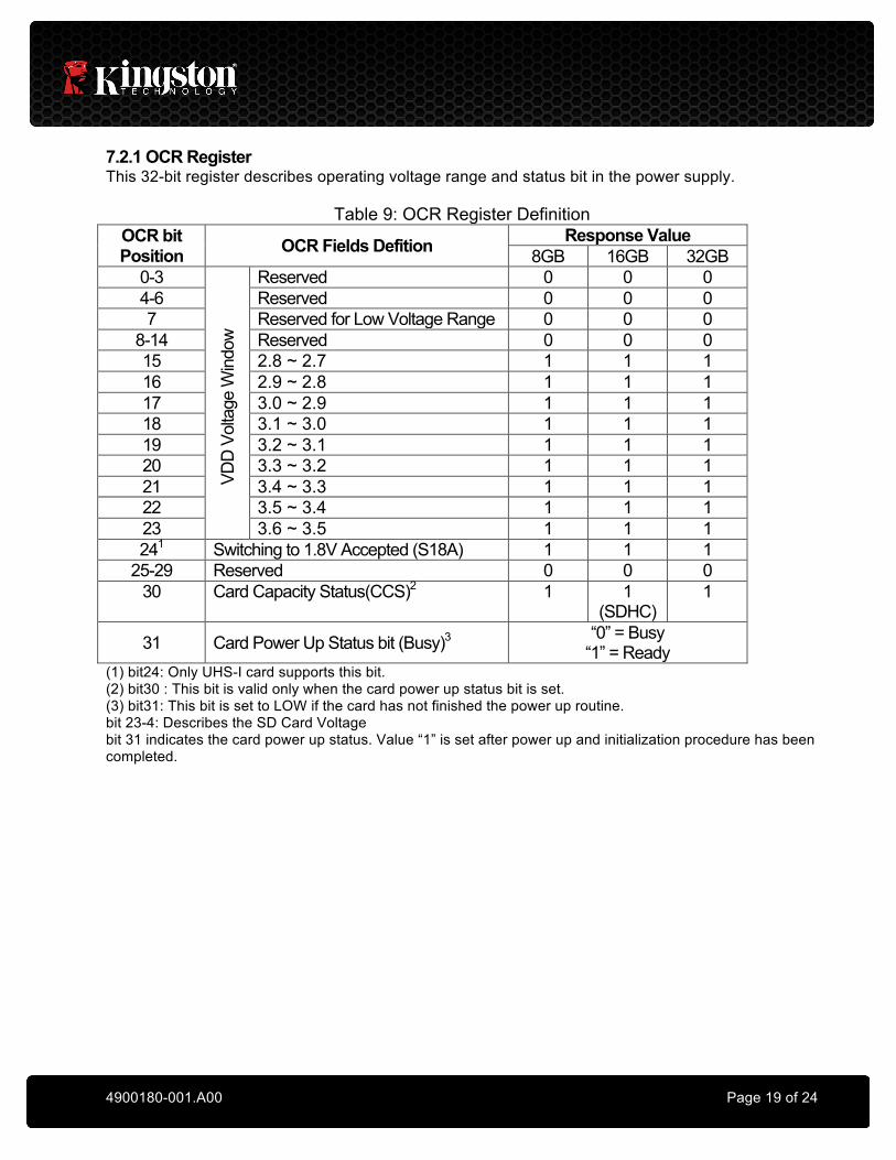
7.2.1 OCR Register This 32-bit register describes operating voltage range and status bit in the power supply.
Table 9: OCR Register Definition OCR bit Position OCR Fields Defition Response Value
8GB 16GB 32GB 0-3
VDD
Vol
tage
Win
dow
Reserved 0 0 0 4-6 Reserved 0 0 0 7 Reserved for Low Voltage Range 0 0 0
8-14 Reserved 0 0 0 15 2.8 ~ 2.7 1 1 1 16 2.9 ~ 2.8 1 1 1 17 3.0 ~ 2.9 1 1 1 18 3.1 ~ 3.0 1 1 1 19 3.2 ~ 3.1 1 1 1 20 3.3 ~ 3.2 1 1 1 21 3.4 ~ 3.3 1 1 1 22 3.5 ~ 3.4 1 1 1 23 3.6 ~ 3.5 1 1 1 241 Switching to 1.8V Accepted (S18A) 1 1 1
25-29 Reserved 0 0 0 30 Card Capacity Status(CCS)2 1 1
(SDHC) 1
31 Card Power Up Status bit (Busy)3 “0” = Busy “1” = Ready
(1) bit24: Only UHS-I card supports this bit. (2) bit30 : This bit is valid only when the card power up status bit is set. (3) bit31: This bit is set to LOW if the card has not finished the power up routine. bit 23-4: Describes the SD Card Voltage bit 31 indicates the card power up status. Value “1” is set after power up and initialization procedure has been completed.
4900180-001.A00 Page 20 of 24
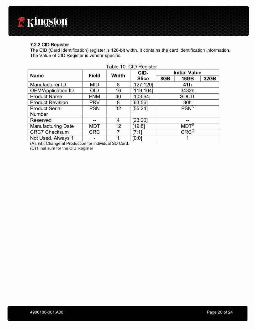
7.2.2 CID Register The CID (Card Identification) register is 128-bit width. It contains the card identification information. The Value of CID Register is vendor specific.
Table 10: CID Register
Name Field Width CID-Slice
Initial Value 8GB 16GB 32GB
Manufacturer ID MID 8 [127:120] 41h OEM/Application ID OID 16 [119:104] 3432h Product Name PNM 40 [103:64] SDCIT Product Revision PRV 8 [63:56] 30h Product Serial Number
PSN 32 [55:24] PSNA
Reserved -- 4 [23:20] -- Manufacturing Date MDT 12 [19:8] MDTB CRC7 Checksum CRC 7 [7:1] CRCC Not Used, Always 1 - 1 [0:0] 1 (A), (B): Change at Production for individual SD Card. (C) Final sum for the CID Register
4900180-001.A00 Page 21 of 24
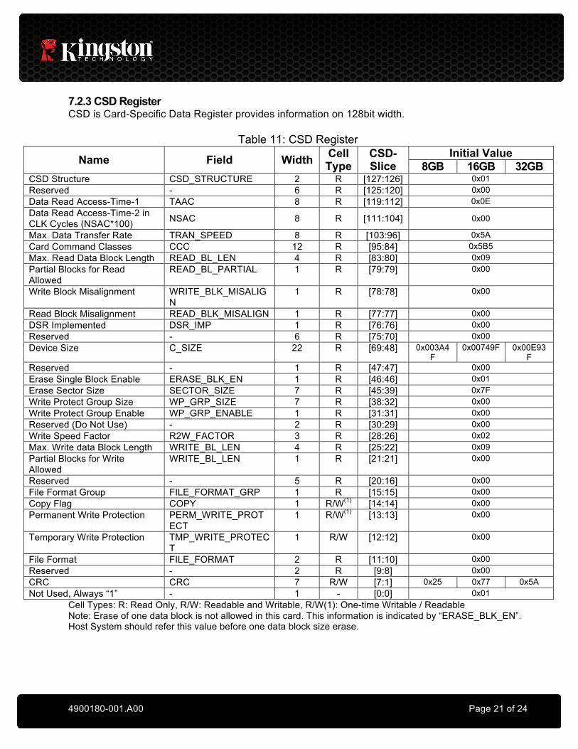
7.2.3 CSD Register CSD is Card-Specific Data Register provides information on 128bit width.
Table 11: CSD Register
Name Field Width Cell Type
CSD-Slice
Initial Value 8GB 16GB 32GB
CSD Structure CSD_STRUCTURE 2 R [127:126] 0x01 Reserved - 6 R [125:120] 0x00 Data Read Access-Time-1 TAAC 8 R [119:112] 0x0E Data Read Access-Time-2 in CLK Cycles (NSAC*100) NSAC 8 R [111:104] 0x00
Max. Data Transfer Rate TRAN_SPEED 8 R [103:96] 0x5A Card Command Classes CCC 12 R [95:84] 0x5B5 Max. Read Data Block Length READ_BL_LEN 4 R [83:80] 0x09 Partial Blocks for Read Allowed
READ_BL_PARTIAL 1 R [79:79] 0x00
Write Block Misalignment WRITE_BLK_MISALIGN
1 R [78:78] 0x00
Read Block Misalignment READ_BLK_MISALIGN 1 R [77:77] 0x00 DSR Implemented DSR_IMP 1 R [76:76] 0x00 Reserved - 6 R [75:70] 0x00 Device Size C_SIZE 22 R [69:48] 0x003A4
F 0x00749F 0x00E93
F Reserved - 1 R [47:47] 0x00 Erase Single Block Enable ERASE_BLK_EN 1 R [46:46] 0x01 Erase Sector Size SECTOR_SIZE 7 R [45:39] 0x7F Write Protect Group Size WP_GRP_SIZE 7 R [38:32] 0x00 Write Protect Group Enable WP_GRP_ENABLE 1 R [31:31] 0x00 Reserved (Do Not Use) - 2 R [30:29] 0x00 Write Speed Factor R2W_FACTOR 3 R [28:26] 0x02 Max. Write data Block Length WRITE_BL_LEN 4 R [25:22] 0x09 Partial Blocks for Write Allowed
WRITE_BL_LEN 1 R [21:21] 0x00
Reserved - 5 R [20:16] 0x00 File Format Group FILE_FORMAT_GRP 1 R [15:15] 0x00 Copy Flag COPY 1 R/W(1) [14:14] 0x00 Permanent Write Protection PERM_WRITE_PROT
ECT 1 R/W(1) [13:13] 0x00
Temporary Write Protection TMP_WRITE_PROTECT
1 R/W [12:12] 0x00
File Format FILE_FORMAT 2 R [11:10] 0x00 Reserved - 2 R [9:8] 0x00 CRC CRC 7 R/W [7:1] 0x25 0x77 0x5A Not Used, Always “1” - 1 - [0:0] 0x01
Cell Types: R: Read Only, R/W: Readable and Writable, R/W(1): One-time Writable / Readable Note: Erase of one data block is not allowed in this card. This information is indicated by “ERASE_BLK_EN”. Host System should refer this value before one data block size erase.
4900180-001.A00 Page 22 of 24
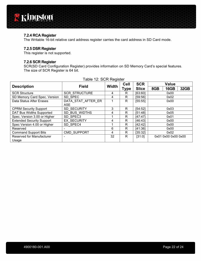
7.2.4 RCA Register The Writable 16-bit relative card address register carries the card address in SD Card mode. 7.2.5 DSR Register This register is not supported. 7.2.6 SCR Register SCR(SD Card Configuration Register) provides information on SD Memory Card’s special features. The size of SCR Register is 64 bit.
Table 12: SCR Register
Description Field Width Cell Type
SCR Slice
Value 8GB 16GB 32GB
SCR Structure SCR_STRUCTURE 4 R [63:60] 0x00 SD Memory Card Spec. Version SD_SPEC 4 R [59:56] 0x02 Data Status After Erases DATA_STAT_AFTER_ER
ASE 1 R [55:55] 0x00
CPRM Security Support SD_SECURITY 3 R [54:52] 0x03 DAT Bus Widths Supported SD_BUS_WIDTHS 4 R [51:48] 0x05 Spec. Version 3.00 or Higher SD_SPEC3 1 R [47:47] 0x01 Extended Security Support EX_SECURITY 4 R [46:43] 0x00 Spec Version 4.00 or Higher SD_SPEC4 1 R [42:42] 0x00 Reserved - 6 R [41:36] 0x00 Command Support Bits CMD_SUPPORT 4 R [35:32] 0x02 Reserved for Manufacturer Usage
- 32 R [31:0] 0x01 0x00 0x00 0x00
4900180-001.A00 Page 23 of 24
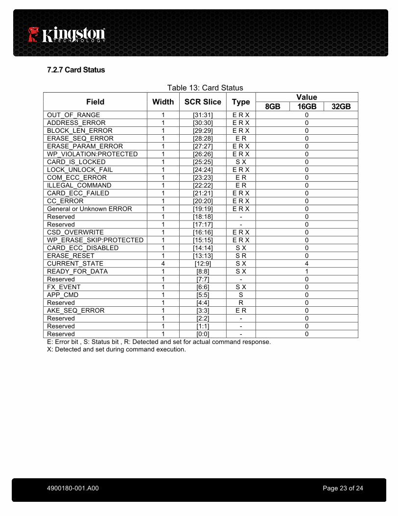
7.2.7 Card Status
Table 13: Card Status
Field Width SCR Slice Type Value 8GB 16GB 32GB
OUT_OF_RANGE 1 [31:31] E R X 0 ADDRESS_ERROR 1 [30:30] E R X 0 BLOCK_LEN_ERROR 1 [29:29] E R X 0 ERASE_SEQ_ERROR 1 [28:28] E R 0 ERASE_PARAM_ERROR 1 [27:27] E R X 0 WP_VIOLATION:PROTECTED 1 [26:26] E R X 0 CARD_IS_LOCKED 1 [25:25] S X 0 LOCK_UNLOCK_FAIL 1 [24:24] E R X 0 COM_ECC_ERROR 1 [23:23] E R 0 ILLEGAL_COMMAND 1 [22:22] E R 0 CARD_ECC_FAILED 1 [21:21] E R X 0 CC_ERROR 1 [20:20] E R X 0 General or Unknown ERROR 1 [19:19] E R X 0 Reserved 1 [18:18] - 0 Reserved 1 [17:17] - 0 CSD_OVERWRITE 1 [16:16] E R X 0 WP_ERASE_SKIP:PROTECTED 1 [15:15] E R X 0 CARD_ECC_DISABLED 1 [14:14] S X 0 ERASE_RESET 1 [13:13] S R 0 CURRENT_STATE 4 [12:9] S X 4 READY_FOR_DATA 1 [8:8] S X 1 Reserved 1 [7:7] - 0 FX_EVENT 1 [6:6] S X 0 APP_CMD 1 [5:5] S 0 Reserved 1 [4:4] R 0 AKE_SEQ_ERROR 1 [3:3] E R 0 Reserved 1 [2:2] - 0 Reserved 1 [1:1] - 0 Reserved 1 [0:0] - 0 E: Error bit , S: Status bit , R: Detected and set for actual command response. X: Detected and set during command execution.
4900180-001.A00 Page 24 of 24
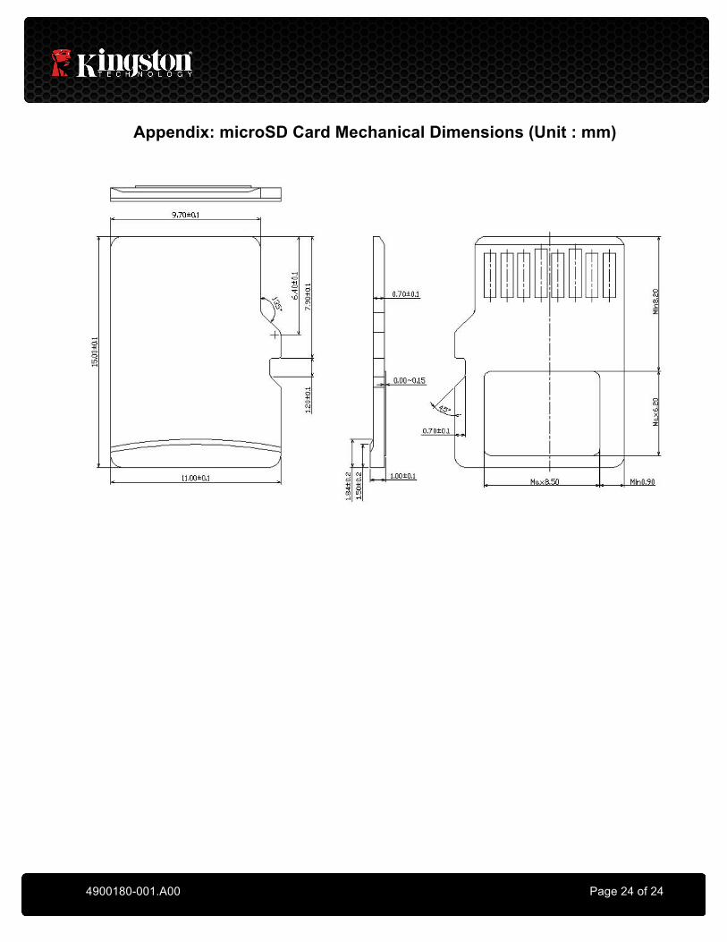
Appendix: microSD Card Mechanical Dimensions (Unit : mm)