Embed Size (px)
Citation preview
1/12September 2001
QUIESCENT CURRENT SPECIFIED UP TO 20V
VERY LOW POWER CONSUMPTION : 70µW (TYP.) AT VCO fo = 10kHz, VDD = 5V
OPERATING FREQUENCY RANGE : UP TO 1.4MHz (TYP.) AT VDD = 10V
LOW FREQUENCY DRIFT : 0.04%/°C (typ.) AT VDD = 10V
CHOICE OF TWO PHASE COMPARATORS :1) EXCLUSIVE - OR NETWORK2) EDGE-CONTROLLED MEMORY NETWORK WITH PHASE-PULSE OUTPUT FOR LOCK INDICATION
HIGH VCO LINEARITY: <1% (TYP.) VCO INHIBIT CONTROL FOR ON-OFF
KEYING AND ULTRA-LOW STANDBY POWER CONSUMPTION
SOURCE-FOLLOWER OUTPUT OF VCO CONTROL INPUT (demod. output)
ZENER DIODE TO ASSIST SUPPLY REGULATION
5V, 10V AND 15V PARAMETRIC RATINGS INPUT LEAKAGE CURRENT
II = 100nA (MAX) AT VDD = 18V TA = 25°C 100% TESTED FOR QUIESCENT CURRENT MEETS ALL REQUIREMENTS OF JEDEC
JESD13B " STANDARD SPECIFICATIONS FOR DESCRIPTION OF B SERIES CMOS DEVICES"
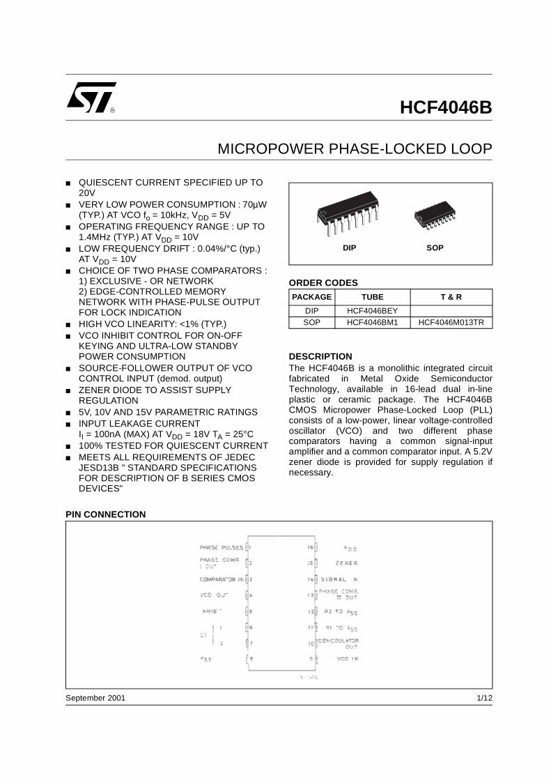
DESCRIPTIONThe HCF4046B is a monolithic integrated circuitfabricated in Metal Oxide SemiconductorTechnology, available in 16-lead dual in-lineplastic or ceramic package. The HCF4046BCMOS Micropower Phase-Locked Loop (PLL)consists of a low-power, linear voltage-controlledoscillator (VCO) and two different phasecomparators having a common signal-inputamplifier and a common comparator input. A 5.2Vzener diode is provided for supply regulation ifnecessary.
HCF4046B
MICROPOWER PHASE-LOCKED LOOP
PIN CONNECTION
ORDER CODES
PACKAGE TUBE T & R
DIP HCF4046BEY
SOP HCF4046BM1 HCF4046M013TR
DIP SOP
HCF4046B
2/12
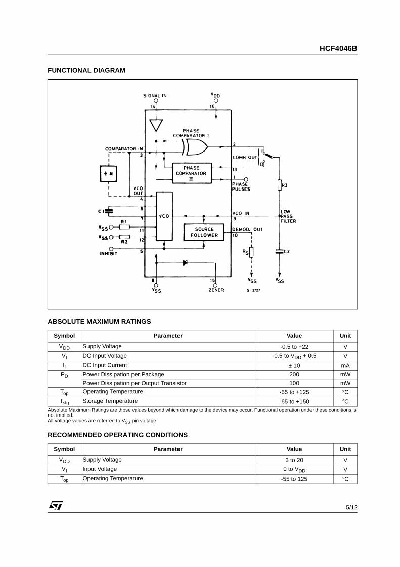
VCO SectionThe VCO requires one external capacitor C1 andone or two external resistors (R1 or R1 and R2).Resistor R1 and capacitor C1 determine thefrequency range of the VCO and resistor R2enables the VCO to have a frequency offset ifrequired. The high input impedance (1012Ω) of theVCO simplifiers the design of low-pass filters bypermitting the designer a wide choice ofresistor-to-capacitor ratios. In order not to load thelow-pass filter, a source-follower output of theVCO input voltage is provided at terminal 10(DEMODULATED OUTPUT). If this terminal isused, a load resistor (RS) of 10 KΩ or more shouldbe connected from this terminal to VSS. If unusedthis terminal should be left open. The VCO can beconnected either directly or through frequencydividers to the comparator input of the phasecomparators. A full CMOS logic swing is availableat the output of the VCO and allows directcoupling to CMOS frequency dividers such as theHCF4024B, HCF4018B, HCF4020B, HCF4022B,HCF4029B and HBF4059A. One or moreHCF4018B (Presettable Divide-by-N Counter) orHCF4029B (Presettable Up/Down Counter), orHBF4059A (Programmable Divide-by-"N"Counter), together with the HCF4046B(Phase-Locked Loop) can be used to build amicropower low-frequency synthesizer. A logic 0on the INHIBIT input "enables" the VCO and thesource follower, while a logic 1 "turns off" both tominimize stand-by power consumption.
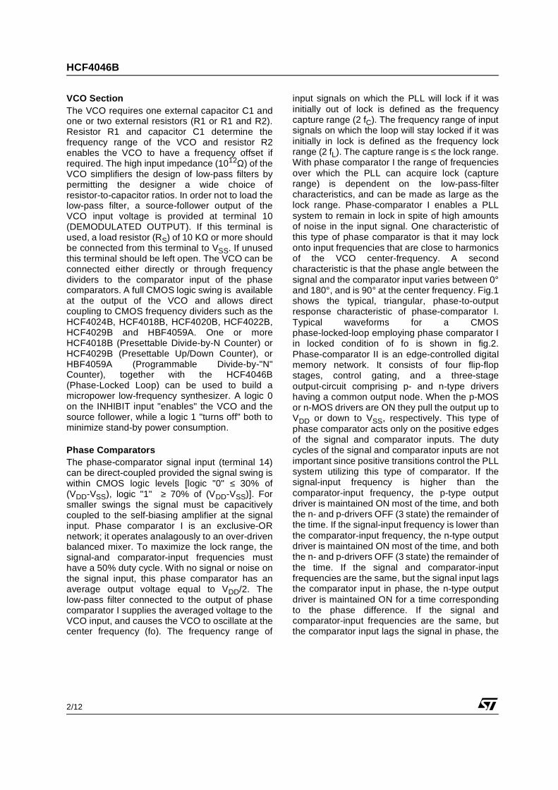
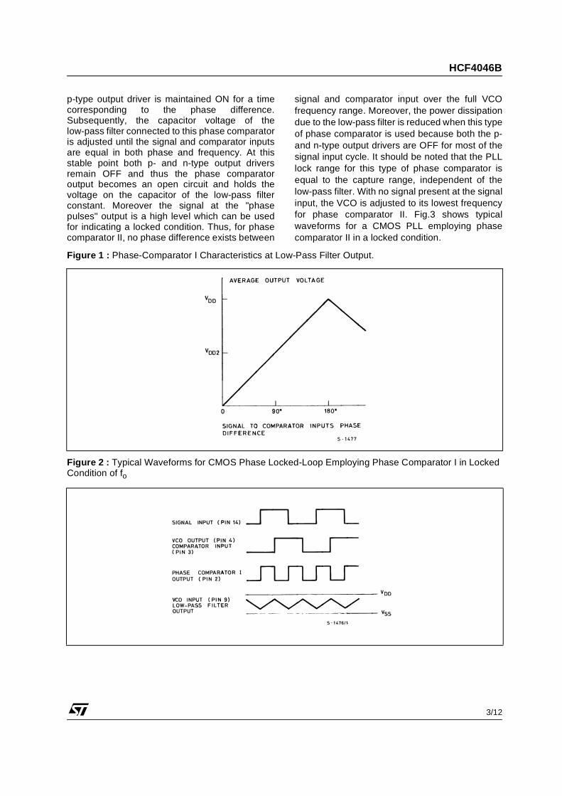
Phase ComparatorsThe phase-comparator signal input (terminal 14)can be direct-coupled provided the signal swing iswithin CMOS logic levels [logic "0" ≤ 30% of(VDD-VSS), logic "1" ≥ 70% of (VDD-VSS)]. Forsmaller swings the signal must be capacitivelycoupled to the self-biasing amplifier at the signalinput. Phase comparator I is an exclusive-ORnetwork; it operates analagously to an over-drivenbalanced mixer. To maximize the lock range, thesignal-and comparator-input frequencies musthave a 50% duty cycle. With no signal or noise onthe signal input, this phase comparator has anaverage output voltage equal to VDD/2. Thelow-pass filter connected to the output of phasecomparator I supplies the averaged voltage to theVCO input, and causes the VCO to oscillate at thecenter frequency (fo). The frequency range of
input signals on which the PLL will lock if it wasinitially out of lock is defined as the frequencycapture range (2 fC). The frequency range of inputsignals on which the loop will stay locked if it wasinitially in lock is defined as the frequency lockrange (2 fL). The capture range is ≤ the lock range.With phase comparator I the range of frequenciesover which the PLL can acquire lock (capturerange) is dependent on the low-pass-filtercharacteristics, and can be made as large as thelock range. Phase-comparator I enables a PLLsystem to remain in lock in spite of high amountsof noise in the input signal. One characteristic ofthis type of phase comparator is that it may lockonto input frequencies that are close to harmonicsof the VCO center-frequency. A secondcharacteristic is that the phase angle between thesignal and the comparator input varies between 0°and 180°, and is 90° at the center frequency. Fig.1shows the typical, triangular, phase-to-outputresponse characteristic of phase-comparator I.Typical waveforms for a CMOSphase-locked-loop employing phase comparator Iin locked condition of fo is shown in fig.2.Phase-comparator II is an edge-controlled digitalmemory network. It consists of four flip-flopstages, control gating, and a three-stageoutput-circuit comprising p- and n-type drivershaving a common output node. When the p-MOSor n-MOS drivers are ON they pull the output up toVDD or down to VSS, respectively. This type ofphase comparator acts only on the positive edgesof the signal and comparator inputs. The dutycycles of the signal and comparator inputs are notimportant since positive transitions control the PLLsystem utilizing this type of comparator. If thesignal-input frequency is higher than thecomparator-input frequency, the p-type outputdriver is maintained ON most of the time, and boththe n- and p-drivers OFF (3 state) the remainder ofthe time. If the signal-input frequency is lower thanthe comparator-input frequency, the n-type outputdriver is maintained ON most of the time, and boththe n- and p-drivers OFF (3 state) the remainder ofthe time. If the signal and comparator-inputfrequencies are the same, but the signal input lagsthe comparator input in phase, the n-type outputdriver is maintained ON for a time correspondingto the phase difference. If the signal andcomparator-input frequencies are the same, butthe comparator input lags the signal in phase, the
HCF4046B
3/12
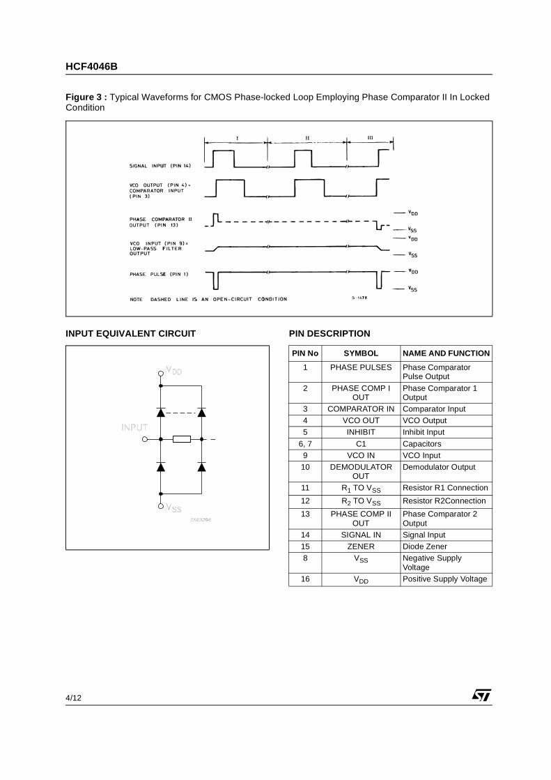
p-type output driver is maintained ON for a timecorresponding to the phase difference.Subsequently, the capacitor voltage of thelow-pass filter connected to this phase comparatoris adjusted until the signal and comparator inputsare equal in both phase and frequency. At thisstable point both p- and n-type output driversremain OFF and thus the phase comparatoroutput becomes an open circuit and holds thevoltage on the capacitor of the low-pass filterconstant. Moreover the signal at the "phasepulses" output is a high level which can be usedfor indicating a locked condition. Thus, for phasecomparator II, no phase difference exists between
signal and comparator input over the full VCOfrequency range. Moreover, the power dissipationdue to the low-pass filter is reduced when this typeof phase comparator is used because both the p-and n-type output drivers are OFF for most of thesignal input cycle. It should be noted that the PLLlock range for this type of phase comparator isequal to the capture range, independent of thelow-pass filter. With no signal present at the signalinput, the VCO is adjusted to its lowest frequencyfor phase comparator II. Fig.3 shows typicalwaveforms for a CMOS PLL employing phasecomparator II in a locked condition.
Figure 1 : Phase-Comparator I Characteristics at Low-Pass Filter Output.
Figure 2 : Typical Waveforms for CMOS Phase Locked-Loop Employing Phase Comparator I in Locked Condition of fo
HCF4046B
4/12
Figure 3 : Typical Waveforms for CMOS Phase-locked Loop Employing Phase Comparator II In Locked Condition
INPUT EQUIVALENT CIRCUIT PIN DESCRIPTION
PIN No SYMBOL NAME AND FUNCTION
1 PHASE PULSES Phase Comparator Pulse Output
2 PHASE COMP I OUT
Phase Comparator 1 Output
3 COMPARATOR IN Comparator Input
4 VCO OUT VCO Output
5 INHIBIT Inhibit Input
6, 7 C1 Capacitors
9 VCO IN VCO Input
10 DEMODULATOR OUT
Demodulator Output
11 R1 TO VSS Resistor R1 Connection
12 R2 TO VSS Resistor R2Connection
13 PHASE COMP II OUT
Phase Comparator 2 Output
14 SIGNAL IN Signal Input
15 ZENER Diode Zener
8 VSS Negative Supply Voltage
16 VDD Positive Supply Voltage
HCF4046B
5/12
FUNCTIONAL DIAGRAM
ABSOLUTE MAXIMUM RATINGS
Absolute Maximum Ratings are those values beyond which damage to the device may occur. Functional operation under these conditions is not implied.All voltage values are referred to VSS pin voltage.
RECOMMENDED OPERATING CONDITIONS
Symbol Parameter Value Unit
VDD Supply Voltage -0.5 to +22 V
VI DC Input Voltage -0.5 to VDD + 0.5 V
II DC Input Current ± 10 mA
PD Power Dissipation per Package 200 mW
Power Dissipation per Output Transistor 100 mW
Top Operating Temperature -55 to +125 °C
Tstg Storage Temperature -65 to +150 °C
Symbol Parameter Value Unit
VDD Supply Voltage 3 to 20 V
VI Input Voltage 0 to VDD V
Top Operating Temperature -55 to 125 °C
HCF4046B
6/12
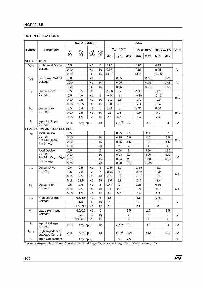
DC SPECIFICATIONS
The Noise Margin for both "1" and "0" level is: 1V min. with VDD=5V, 2V min. with VDD=10V, 2.5V min. with VDD=15V
Symbol Parameter
Test Condition Value
UnitVI(V)
VO(V)
|IO|(µA)
VDD(V)
TA = 25°C -40 to 85°C -55 to 125°C
Min. Typ. Max. Min. Max. Min. Max.
VCO SECTIONVOH High Level Output
Voltage0/5 <1 5 4.95 4.95 4.95
V0/10 <1 10 9.95 9.95 9.95
0/15 <1 15 14.95 14.95 14.95
VOL Low Level Output Voltage
5/0 <1 5 0.05 0.05 0.05
V10/0 <1 10 0.05 0.05 0.05
15/0 <1 15 0.05 0.05 0.05
IOH Output Drive Current
0/5 2.5 <1 5 -1.36 -3.2 -1.15 -1.1
mA0/5 4.6 <1 5 -0.44 -1 -0.36 -0.36
0/10 9.5 <1 10 -1.1 -2.6 -0.9 -0.9
0/15 13.5 <1 15 -3.0 -6.8 -2.4 -2.4
IOL Output Sink Current
0/5 0.4 <1 5 0.44 1 0.36 0.36
mA0/10 0.5 <1 10 1.1 2.6 0.9 0.9
0/15 1.5 <1 15 3.0 6.8 2.4 2.4
II Input Leakage Current
0/18 Any Input 18 ±10-5 ±0.1 ±1 ±1 µA
PHASE COMPARATOR SECTIONIDD Total Device
CurrentPin 14= OpenPin 5= VDD
0/5 5 0.05 0.1 0.1 0.1
mA0/10 10 0.25 0.5 0.5 0.5
0/15 15 0.75 1.5 1.5 1.5
0/20 20 2 4 4 4
Total Device CurrentPin 14= VSS or VDDPin 5= VDD
0/5 5 0.04 5 150 150
µA0/10 10 0.04 10 300 300
0/15 15 0.04 20 600 600
0/20 20 0.08 100 3000
IOH Output Drive Current
0/5 2.5 <1 5 -1.36 -3.2 -1.15 -1.1
mA0/5 4.6 <1 5 -0.44 -1 -0.36 -0.36
0/10 9.5 <1 10 -1.1 -2.6 -0.9 -0.9
0/15 13.5 <1 15 -3.0 -6.8 -2.4 -2.4
IOL Output Sink Current
0/5 0.4 <1 5 0.44 1 0.36 0.36
mA0/10 0.5 <1 10 1.1 2.6 0.9 0.9
0/15 1.5 <1 15 3.0 6.8 2.4 2.4
VIH High Level Input Voltage
0.5/4.5 <1 5 3.5 3.5 3.5
V1/9 <1 10 7 7 7
1.5/13.5 <1 15 11 11 11
VIL Low Level Input Voltage
4.5/0.5 <1 5 1.5 1.5 1.5
V9/1 <1 10 3 3 3
13.5/1.5 <1 15 4 4 4
II Input Leakage Current
0/18 Any Input 18 ±10-5 ±0.1 ±1 ±1 µA
IOUT High Impedance Leakage Current 0/18 Any Input 18 ±10-4 ±0.4 ±12 ±12 µA
CI Input Capacitance Any Input 5 7.5 pF
HCF4046B
7/12
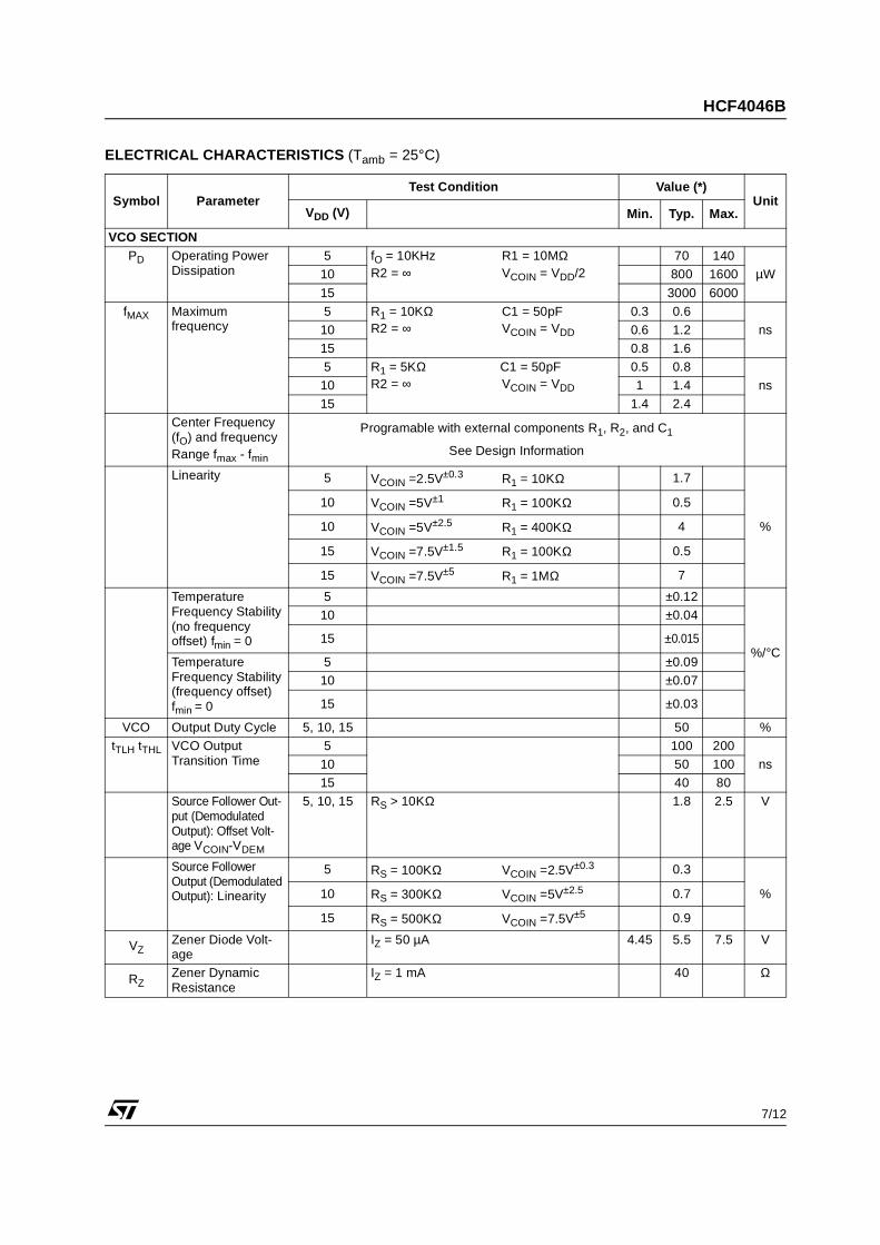
ELECTRICAL CHARACTERISTICS (Tamb = 25°C)
Symbol ParameterTest Condition Value (*)
UnitVDD (V) Min. Typ. Max.
VCO SECTIONPD Operating Power
Dissipation 5 fO = 10KHz R1 = 10MΩ
R2 = ∞ VCOIN = VDD/270 140
µW10 800 1600
15 3000 6000
fMAX Maximum frequency
5 R1 = 10KΩ C1 = 50pFR2 = ∞ VCOIN = VDD
0.3 0.6
ns10 0.6 1.2
15 0.8 1.6
5 R1 = 5KΩ C1 = 50pFR2 = ∞ VCOIN = VDD
0.5 0.8
ns10 1 1.4
15 1.4 2.4
Center Frequency (fO) and frequency Range fmax - fmin
Programable with external components R1, R2, and C1
See Design Information
Linearity 5 VCOIN =2.5V±0.3 R1 = 10KΩ 1.7
%
10 VCOIN =5V±1 R1 = 100KΩ 0.5
10 VCOIN =5V±2.5 R1 = 400KΩ 4
15 VCOIN =7.5V±1.5 R1 = 100KΩ 0.5
15 VCOIN =7.5V±5 R1 = 1MΩ 7
Temperature Frequency Stability (no frequency offset) fmin = 0
5 ±0.12
%/°C
10 ±0.04
15 ±0.015
Temperature Frequency Stability (frequency offset) fmin = 0
5 ±0.09
10 ±0.07
15 ±0.03
VCO Output Duty Cycle 5, 10, 15 50 %
tTLH tTHL VCO Output Transition Time
5 100 200
ns10 50 100
15 40 80Source Follower Out-put (Demodulated Output): Offset Volt-age VCOIN-VDEM
5, 10, 15 RS > 10KΩ 1.8 2.5 V
Source Follower Output (Demodulated Output): Linearity
5 RS = 100KΩ VCOIN =2.5V±0.3 0.3
%10 RS = 300KΩ VCOIN =5V±2.5 0.7
15 RS = 500KΩ VCOIN =7.5V±5 0.9
VZZener Diode Volt-age
IZ = 50 µA 4.45 5.5 7.5 V
RZZener Dynamic Resistance
IZ = 1 mA 40 Ω
HCF4046B
8/12
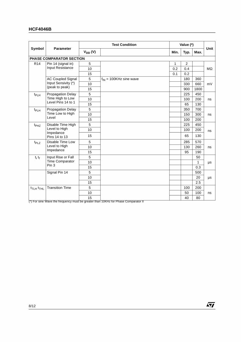
(*) For sine Wave the frequency must be greater than 10KHz for Phase Comparator II
PHASE COMPARATOR SECTIONR14 Pin 14 (signal in)
Input Resistance 5 1 2
MΩ10 0.2 0.4
15 0.1 0.2
AC Coupled Signal Input Sensivity (*) (peak to peak)
5 fIN = 100KHz sine wave 180 360
mV10 330 660
15 900 1800
tPLH Propagation Delay Time High to Low Level Pins 14 to 1
5 225 450
ns10 100 200
15 65 130
tPLH Propagation Delay Time Low to High Level
5 350 700
ns10 150 300
15 100 200
tPHZ Disable Time High Level to High Impedance Pins 14 to 13
5 225 450
ns10 100 200
15 65 130
tPLZ Disable Time Low Level to High Impedance
5 285 570
ns10 130 260
15 95 190
tr tf Input Rise or Fall Time Comparator Pin 3
5 50
µs10 1
15 0.3
Signal Pin 14 5 500
µs10 20
15 2.5
tTLH tTHL Transition Time 5 100 200
ns10 50 100
15 40 80
Symbol ParameterTest Condition Value (*)
UnitVDD (V) Min. Typ. Max.
HCF4046B
9/12
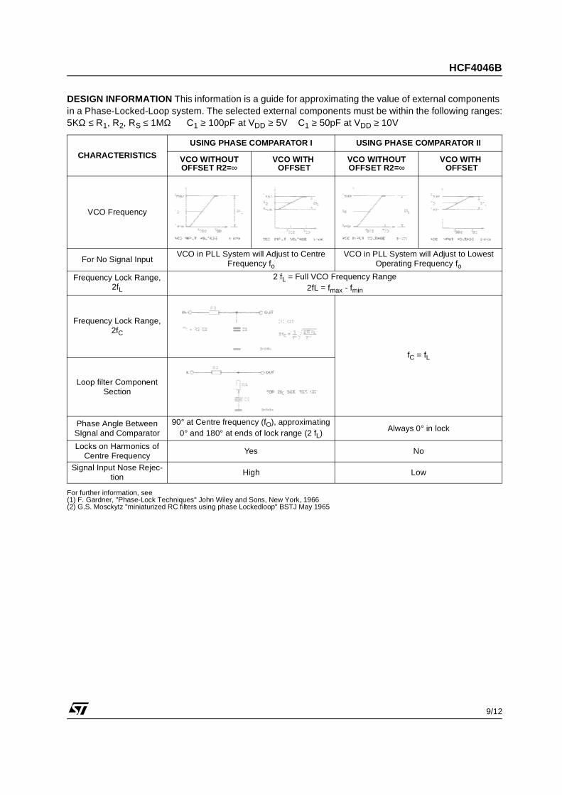
DESIGN INFORMATION This information is a guide for approximating the value of external components in a Phase-Locked-Loop system. The selected external components must be within the following ranges:5KΩ ≤ R1, R2, RS ≤ 1MΩ C1 ≥ 100pF at VDD ≥ 5V C1 ≥ 50pF at VDD ≥ 10V
For further information, see(1) F. Gardner, "Phase-Lock Techniques" John Wiley and Sons, New York, 1966(2) G.S. Mosckytz "miniaturized RC filters using phase Lockedloop" BSTJ May 1965
CHARACTERISTICS
USING PHASE COMPARATOR I USING PHASE COMPARATOR II
VCO WITHOUT OFFSET R2=∞
VCO WITH OFFSET
VCO WITHOUT OFFSET R2=∞
VCO WITH OFFSET
VCO Frequency
For No Signal InputVCO in PLL System will Adjust to Centre
Frequency foVCO in PLL System will Adjust to Lowest
Operating Frequency fo
Frequency Lock Range, 2fL
2 fL = Full VCO Frequency Range2fL = fmax - fmin
Frequency Lock Range, 2fC
fC = fL
Loop filter Component Section
Phase Angle Between SIgnal and Comparator
90° at Centre frequency (fO), approximating 0° and 180° at ends of lock range (2 fL)
Always 0° in lock
Locks on Harmonics of Centre Frequency
Yes No
Signal Input Nose Rejec-tion
High Low
HCF4046B
10/12
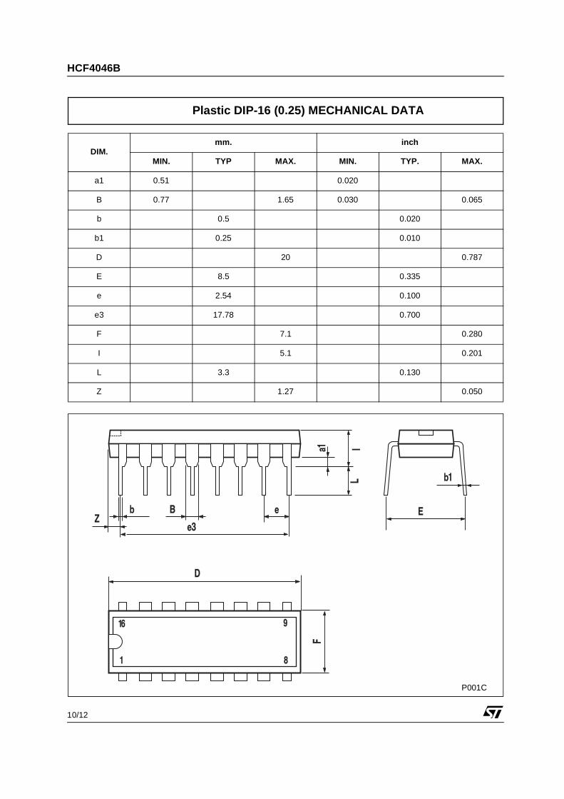
DIM.mm. inch
MIN. TYP MAX. MIN. TYP. MAX.
a1 0.51 0.020
B 0.77 1.65 0.030 0.065
b 0.5 0.020
b1 0.25 0.010
D 20 0.787
E 8.5 0.335
e 2.54 0.100
e3 17.78 0.700
F 7.1 0.280
I 5.1 0.201
L 3.3 0.130
Z 1.27 0.050
Plastic DIP-16 (0.25) MECHANICAL DATA
P001C
HCF4046B
11/12
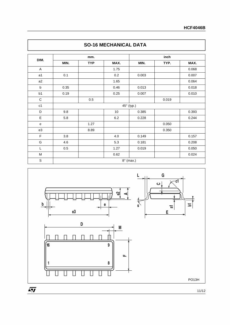
DIM.mm. inch
MIN. TYP MAX. MIN. TYP. MAX.
A 1.75 0.068
a1 0.1 0.2 0.003 0.007
a2 1.65 0.064
b 0.35 0.46 0.013 0.018
b1 0.19 0.25 0.007 0.010
C 0.5 0.019
c1 45° (typ.)
D 9.8 10 0.385 0.393
E 5.8 6.2 0.228 0.244
e 1.27 0.050
e3 8.89 0.350
F 3.8 4.0 0.149 0.157
G 4.6 5.3 0.181 0.208
L 0.5 1.27 0.019 0.050
M 0.62 0.024
S 8° (max.)
SO-16 MECHANICAL DATA
PO13H
HCF4046B
12/12
Information furnished is believed to be accurate and reliable. However, STMicroelectronics assumes no responsibility for theconsequences of use of such information nor for any infringement of patents or other rights of third parties which may result fromits use. No license is granted by implication or otherwise under any patent or patent rights of STMicroelectronics. Specificationsmentioned in this publication are subject to change without notice. This publication supersedes and replaces all informationpreviously supplied. STMicroelectronics products are not authorized for use as critical components in life support devices orsystems without express written approval of STMicroelectronics.
© The ST logo is a registered trademark of STMicroelectronics
© 2001 STMicroelectronics - Printed in Italy - All Rights ReservedSTMicroelectronics GROUP OF COMPANIES
Australia - Brazil - China - Finland - France - Germany - Hong Kong - India - Italy - Japan - Malaysia - Malta - Morocco Singapore - Spain - Sweden - Switzerland - United Kingdom
© http://www.st.com