Embed Size (px)
Citation preview
MICROPATTERNABLE ELASTIC CARBON NANOTUBE/PDMS ELECTRETS
Wenjun Xu1, Michael Kranz2, Seong-Hyok Kim2, and Mark G. Allen2 1School of Polymer, Textile and Fiber Engineering
2School of Electrical and Computer Engineering, Georgia Institute of Technology, Atlanta, USA Abstract: This paper reports the fabrication and performance of an elastic electret based on polydimethylsiloxane (PDMS)/carbon-nanotube (CNT) composites. The composite formulation concentrates CNTs near the surface of the PDMS and thereby combines the excellent electrical properties and room-temperature micropatternability of the CNT with the elasticity of PDMS. The material was corona-charged and the charge storage behavior was characterized using surface potential measurements. Substantial improvements in charge storage capacity and stability were observed compared to either pure PDMS or CNTs on the surface of PDMS at room temperature over a 280 hour measurement period. Keywords: Elastic electret, Carbon nanotube/PDMS composite, Micropatterning INTRODUCTION
Electrets have broad applications in microphones, micro power generators, piezoelectric sensors/ actuators, microfluidic devices, biomedical implants, and organic field effect transistor memories [1]. Traditional electret materials such as silicon dioxide/silicon nitride, and thin film fluoropolymers such as Teflon AF® and CYTOP®, possess key electret properties of high surface charge density and long-term charge stability. However, it is a challenge to deploy those materials in applications requiring good micropatternability, low processing temperature, and mechanical flexibility. Squeezable/elastic electrets may expand the utility of electrets in many applications, including energy harvesters that tap environmental sources such as human or object motion to generate power. Furthermore, the use of an elastomer in electrets can enhance piezoelectric transduction. The piezoelectric modulus of an electret, d33, can be determined by the following equation [2]:
33 2 /s yd Eησ= (1)
where σs is the surface charge density and Ey is the Young’s modulus of the material. Therefore, a lower Ey can lead to a higher d33. Most traditional polymeric electrets have a relatively high Ey, typically in the range of 1-10GPa. Elastomeric materials have a much lower Ey, typically several MPa.
Patterns of electrostatic charges have been used in conventional xerography and can serve as templates to induce self-assembly and patterning of DNA, proteins and nanoparticles [3]. Moreover, patterned electrets have also demonstrated promising application in electrostatic motors and non-contact electrostatic micro-bearings [4].
This paper proposes a material, suitable for electret formation, which can be viewed as a specially constructed PDMS/CNTs composite. PDMS is an elastic, low cost, easily processible and bio-compatible insulator with a low Young’s modulus of 1-5 MPa and a high dielectric strength of 20kV/mm. Carbon nanotubes exhibit excellent electrical properties with a charge density of 0.24mC/m2 for an individual tube [5] and can be micropatterned at room temperature [6]. The material proposed herein, the micropatterned PDMS/CNTs composite, combines these two non-electret materials into a structure that can trap/store charges, allowing its potential utilization as a micropatternable elastic electret. EXPRIMENTAL Fabrication of CNT/PDMS composite
Figure 1 depicts the fabrication process of the proposed electret material. Room-temperature micropatterning of CNTs was achieved by electrophoretic deposition (EPD). Multi-wall CNTs (Nanostructured & Amorphous Materials, Inc. 95+%) were acidified in a mixture of concentrated sulfuric acid and nitric acid to facilitate the EPD process. Silicon substrates containing desired microstructures and a patterned gold seed layer were fabricated as the templates for EPD. The microstructure-bearing substrates (anode) and a copper counter electrode (cathode) were immersed in a CNT aqueous dispersion (0.1mg/ml) and electrically energized with an electric field of 20V/cm. The deposited mass, and therefore the thickness of the CNT layer, can be determined by the experiment duration for a given microstructure/dispersion deposition.
The fabricated micropatterns of the CNTs were then transferred to a PDMS matrix by pouring liquid PDMS
PowerMEMS 2009, Washington DC, USA, December 1-4, 20090-9743611-5-1/PMEMS2009/$20©2009TRF 177
precursor (Sylgard 184, Dow Corning) into the CNT micropatterns, curing it at 120 ºC for 40min, followed by demolding the PDMS (Fig. 1a). Upon demolding, the CNT layer is transferred to the elastomeric PDMS film (Fig. 1b). Further details of the experiments and discussion of micropatterning of CNTs by EPD, as well as transfer micromolding with PDMS, have been previously reported [6]. A gold layer was then evaporated onto the non-CNT-bearing side of the PDMS sheet, serving as the backside electrode for the electret where the compensation charge may reside (Fig. 1c).
Fig. 1: Scheme of the fabrication process for elastic CNTs/PDMs/Au composite: (a) molding of micropatterned CNTs, (b) transfer micromolding of CNT micropattern, and (c) deposition of gold backside electrode. Corona charging
Negative charges were implanted into the sample films with a point-to-plane corona discharge method (Fig. 2). The sample was placed on a grounded metal plate under a stainless steel needle electrode inside an oven heated to 100 ºC. The distance between the tip of needle and the grounded plate was maintained at 15mm. A constant voltage of -10kV was then applied to the needle electrode for an hour. Afterwards, the sample was first allowed to cool down to room temperature before the voltage was turned off. The decay of the surface charge density of the sample was
then investigated by a surface potential voltmeter (Surface DC Voltmeter model SVM2, AlphaLab. Inc.)
Fig. 2: Scheme of the corona discharging process.
Scanning Electron Microscopy (SEM) (Zeiss, Ultra60) was exploited to study the morphology of the CNT micropatterns and PDMS/CNTs composite structure. Energy-dispersive X-ray spectroscopy (EDS) was utilized to characterize the elemental composition of the topmost surface of the PDMS/CNTs composite. RESULTS AND DISCUSSION
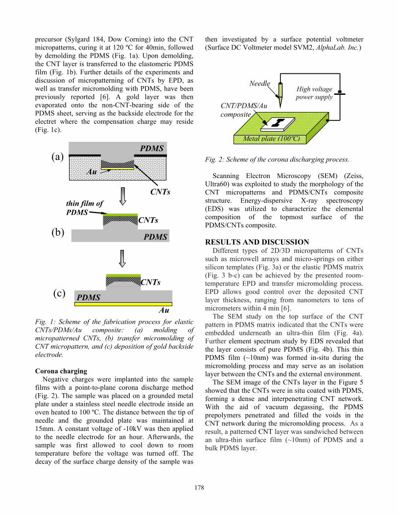
Different types of 2D/3D micropatterns of CNTs such as microwell arrays and micro-springs on either silicon templates (Fig. 3a) or the elastic PDMS matrix (Fig. 3 b-c) can be achieved by the presented room-temperature EPD and transfer micromolding process. EPD allows good control over the deposited CNT layer thickness, ranging from nanometers to tens of micrometers within 4 min [6].
The SEM study on the top surface of the CNT pattern in PDMS matrix indicated that the CNTs were embedded underneath an ultra-thin film (Fig. 4a). Further element spectrum study by EDS revealed that the layer consists of pure PDMS (Fig. 4b). This thin PDMS film (~10nm) was formed in-situ during the micromolding process and may serve as an isolation layer between the CNTs and the external environment.
The SEM image of the CNTs layer in the Figure 5 showed that the CNTs were in situ coated with PDMS, forming a dense and interpenetrating CNT network. With the aid of vacuum degassing, the PDMS prepolymers penetrated and filled the voids in the CNT network during the micromolding process. As a result, a patterned CNT layer was sandwiched between an ultra-thin surface film (~10nm) of PDMS and a bulk PDMS layer.
Metal plate (100ºC)
High voltage power supply
Needle
CNT/PDMS/Au composite
PDMS
CNTs
PDMS
CNTs
CNTs
Au PDMS
thin film of PDMS
Au
PDMS
(c)
(b)
(a)
178
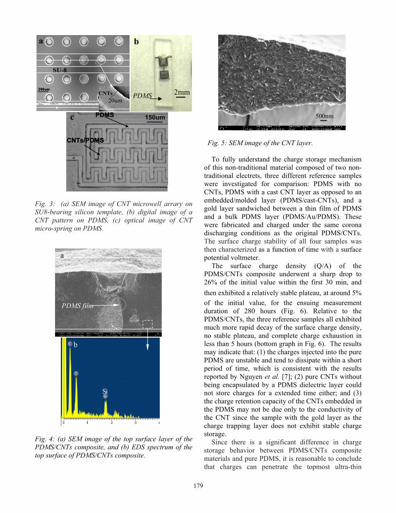
Fig. 3: (a) SEM image of CNT microwell arrary on SU8-bearing silicon template, (b) digital image of a CNT pattern on PDMS, (c) optical image of CNT micro-spring on PDMS.
Fig. 4: (a) SEM image of the top surface layer of the PDMS/CNTs composite, and (b) EDS spectrum of the top surface of PDMS/CNTs composite.
Fig. 5: SEM image of the CNT layer.
To fully understand the charge storage mechanism of this non-traditional material composed of two non-traditional electrets, three different reference samples were investigated for comparison: PDMS with no CNTs, PDMS with a cast CNT layer as opposed to an embedded/molded layer (PDMS/cast-CNTs), and a gold layer sandwiched between a thin film of PDMS and a bulk PDMS layer (PDMS/Au/PDMS). These were fabricated and charged under the same corona discharging conditions as the original PDMS/CNTs. The surface charge stability of all four samples was then characterized as a function of time with a surface potential voltmeter.
The surface charge density (Q/A) of the PDMS/CNTs composite underwent a sharp drop to 26% of the initial value within the first 30 min, and then exhibited a relatively stable plateau, at around 5% of the initial value, for the ensuing measurement duration of 280 hours (Fig. 6). Relative to the PDMS/CNTs, the three reference samples all exhibited much more rapid decay of the surface charge density, no stable plateau, and complete charge exhaustion in less than 5 hours (bottom graph in Fig. 6). The results may indicate that: (1) the charges injected into the pure PDMS are unstable and tend to dissipate within a short period of time, which is consistent with the results reported by Nguyen et al. [7]; (2) pure CNTs without being encapsulated by a PDMS dielectric layer could not store charges for a extended time either; and (3) the charge retention capacity of the CNTs embedded in the PDMS may not be due only to the conductivity of the CNT since the sample with the gold layer as the charge trapping layer does not exhibit stable charge storage.
Since there is a significant difference in charge storage behavior between PDMS/CNTs composite materials and pure PDMS, it is reasonable to conclude that charges can penetrate the topmost ultra-thin
500nm
20umCNTs
SU-8
20umCNTs
SU-8
20umCNTs
SU-8
a
2mm
b
PDMS
CNTs/PDMS
150umPDMS
CNTs/PDMS
PDMS
CNTs/PDMS
150umc
PDMS
PDMS film
SiSi
a
b
179
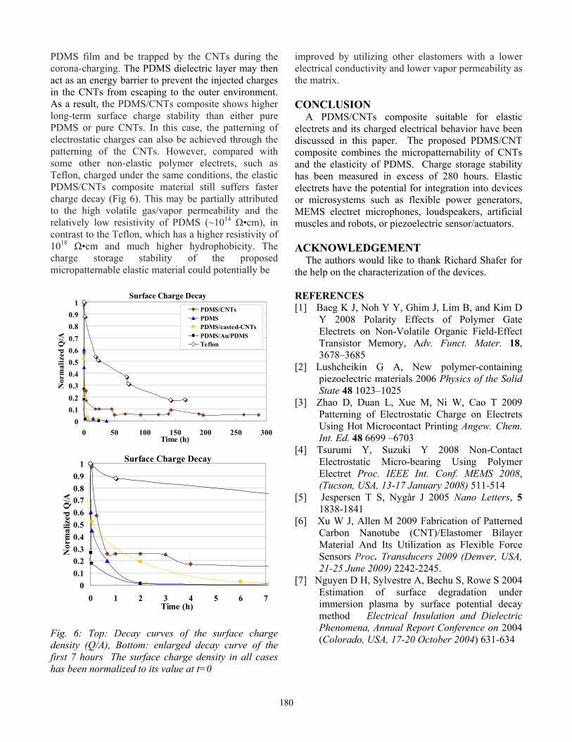
PDMS film and be trapped by the CNTs during the corona-charging. The PDMS dielectric layer may then act as an energy barrier to prevent the injected charges in the CNTs from escaping to the outer environment. As a result, the PDMS/CNTs composite shows higher long-term surface charge stability than either pure PDMS or pure CNTs. In this case, the patterning of electrostatic charges can also be achieved through the patterning of the CNTs. However, compared with some other non-elastic polymer electrets, such as Teflon, charged under the same conditions, the elastic PDMS/CNTs composite material still suffers faster charge decay (Fig 6). This may be partially attributed to the high volatile gas/vapor permeability and the relatively low resistivity of PDMS (~1014 Ω•cm), in contrast to the Teflon, which has a higher resistivity of 1018 Ω•cm and much higher hydrophobicity. The charge storage stability of the proposed micropatternable elastic material could potentially be
Surface Charge Decay
00.10.20.30.40.50.60.70.80.9
1
0 50 100 150 200 250 300Time (h)
Nor
mal
ized
Q/A
PDMS/CNTsPDMSPDMS/casted-CNTsPDMS/Au/PDMSTeflon
Surface Charge Decay
00.10.20.30.40.50.60.70.80.9
1
0 1 2 3 4 5 6 7Time (h)
Nor
mal
ized
Q/A
Fig. 6: Top: Decay curves of the surface charge density (Q/A), Bottom: enlarged decay curve of the first 7 hours The surface charge density in all cases has been normalized to its value at t=0
improved by utilizing other elastomers with a lower electrical conductivity and lower vapor permeability as the matrix. CONCLUSION
A PDMS/CNTs composite suitable for elastic electrets and its charged electrical behavior have been discussed in this paper. The proposed PDMS/CNT composite combines the micropatternability of CNTs and the elasticity of PDMS. Charge storage stability has been measured in excess of 280 hours. Elastic electrets have the potential for integration into devices or microsystems such as flexible power generators, MEMS electret microphones, loudspeakers, artificial muscles and robots, or piezoelectric sensor/actuators. ACKNOWLEDGEMENT
The authors would like to thank Richard Shafer for the help on the characterization of the devices. REFERENCES [1] Baeg K J, Noh Y Y, Ghim J, Lim B, and Kim D
Y 2008 Polarity Effects of Polymer Gate Electrets on Non-Volatile Organic Field-Effect Transistor Memory, Adv. Funct. Mater. 18, 3678–3685
[2] Lushcheikin G A, New polymer-containing piezoelectric materials 2006 Physics of the Solid State 48 1023–1025
[3] Zhao D, Duan L, Xue M, Ni W, Cao T 2009 Patterning of Electrostatic Charge on Electrets Using Hot Microcontact Printing Angew. Chem. Int. Ed. 48 6699 –6703
[4] Tsurumi Y, Suzuki Y 2008 Non-Contact Electrostatic Micro-bearing Using Polymer Electret Proc. IEEE Int. Conf. MEMS 2008, (Tucson, USA, 13-17 January 2008) 511-514
[5] Jespersen T S, Nygår J 2005 Nano Letters, 5 1838-1841
[6] Xu W J, Allen M 2009 Fabrication of Patterned Carbon Nanotube (CNT)/Elastomer Bilayer Material And Its Utilization as Flexible Force Sensors Proc. Transducers 2009 (Denver, USA, 21-25 June 2009) 2242-2245.
[7] Nguyen D H, Sylvestre A, Bechu S, Rowe S 2004 Estimation of surface degradation under immersion plasma by surface potential decay method Electrical Insulation and Dielectric Phenomena, Annual Report Conference on 2004 (Colorado, USA, 17-20 October 2004) 631-634
180