Embed Size (px)
Citation preview
Received: 13 January 2009, Revised: 10 March 2009, Accepted: 10 March 2009, Published online in Wiley InterScience: 4 May 2009
Microfluidic chip fabrication using hotembossing and thermal bonding of COP
Boe-Yu Pemga, Chih-Wei Wub, Yung-Kang Shenc* and Yi Lind
The application of silicon mold inserts by micro-hot embossing molding has been explored in microfluidic chipfabrication. For themold insert, this study employed an SU-8 photoresist to coat the siliconwafer. Ultraviolet light wasthen used to expose the pattern on the SU-8 photoresist surface. This study replicates themicrostructure of the siliconmold insert by micro-hot embossing molding. Different processing parameters (embossing temperature, embossingpressure, embossing time, and de-molding temperature) for the cycle-olefin polymer (COP) film of microfluidic chipsare evaluated. The results showed that the most important parameter for replication of molded microfluidic chip isembossing temperature. De-molding temperature is the most important parameter for surface roughness of themolded microfluidic chip. Themicrochannel is bonded with a cover by thermal bonding processing to form the sealedmicrofluidic chip. The bonding temperature is the most important factor in the bonding strength of the sealedmicrofluidic chip. Copyright � 2009 John Wiley & Sons, Ltd.
Keywords: microfluidic chip; surface roughness; bonding strength; replication; EDS
INTRODUCTION
Microfluidic chip fabrication techniques have been extremelyinnovative in recent decades. Transport phenomena in micro andnanofluidic channel networks are a new frontier in fluid dynamicsresearch. The microfluidic channels of such microdevices aremostly composed of silicon, glass, or quartz and are typicallyfabricated by photolithographic, wet chemical etching, and coverbonding procedures. Chou and Kraus [1] used the silicon moldinsert to fabricate a nanostructure with a width of 10 nm and anaspect ratio of 4. The results showed that the silicon mold insertcould be used up to 30 times. Kricka et al.[2] developed the plasticmicrochips with microchannels (100mm wide, 40mm deep)fabricating in PMMA material by a hot embossing process. Theyused the electroform tool starting with silicon masters andhot-embossed chips were capped with the PMMA top using asolvent bonding process. Narasimhan and Papautsky [3]
described a simple and rapid process of fabricating hotembossing tools using PDMS, which are used to rapidly fabricatethemicrochannel in PMMA. The aspect ratios of PMMA embossedmicrochannel are up to 2, with depths from 5 to 258mm andwidth over 40mm.[4] used the CO2-laser micromachining to formmicrochannels on PMMA substrates. Channel depths were from50 to 1500mm and widths from 150 to 400mm. The thermalbonding process with high temperature and low bondingpressure had been developed for assembling PMMA sheets. Ahigh bonding strength of 2.15MPa is achieved. Fredricksonet al.[5] indicated the fabrication process parameters includingcompression rate, molding temperature, and the compressionforce to discuss the microfuidic devices (cyclic olefin copolymer(COC) material) properties. The results showed that stresswhitening on the device surface was found to be related towelding temperature and the cooling rate of the mold/deviceassembly. The bond strength between the layers of a laminateddevice was determined to be a function of the laminationtemperature. Caneron et al.[6] indicated the thermoforming of
thermoplastic polymers (PMMA, polycarbonate (PC), and PCO) forthe hot embossing lithographic (HEL) fabrication of microfluidicchips. The results appeared that cycle times can be reduced byincreasing the embossing force, but in the absence of anappropriate annealing step, residual stresses can be trapped inthe plastic material. Higher embossing temperatures reduce theviscosity of the polymer melt and allow for lower forces andshorter embossing plateaux. Cho et al.[7] developed a new microfabrication method termed electrochemical fabrication (ECF) tofabricate the stainless steel (SUS) mold. The plastic replica(PMMA) was fabricated using ECF-SUS mold with an injectionmolding process at a mold temperature of 1208C, at a resintemperature of 3508C, pressure of 72–78 kg cm�2, for 3 sec.Quaglio et al.[8] described a characterization methodology of amicrofluidic chips scheme, based on polydimethylsiloxane
(www.interscience.wiley.com) DOI: 10.1002/pat.1447
Research Article
* Correspondence to: Y. K. Shen, School of Dental Technology, Taipei MedicalUniversity, Taipei 110, Taiwan, ROC.E-mail: [email protected]
a B. Y. Pemg
Department of Dentistry, Taipei Medical University Hospital, Taipei 110,
Taiwan, ROC.
b C. W. Wu
Department of Mechanical and Mechatronic Engineering, National Taiwan
Ocean University, Keelung 234, Taiwan, ROC
c Y. K. Shen
School of Dental Technology, Taipei Medical University, Taipei 110, Taiwan,
ROC.
d Y. Lin
Department of Business Administration, Takming University of Science and
Technology, Taipei 104, Taiwan, ROC.
Contract/grant sponsor: National Science Council of the Republic of China,
Taiwan; contract/grant number: NSC 93-2218-E-262-001.
Contract/grant sponsor: Taipei Medical University, Taiwan; contract/grant
number: TMU96-AE1-B17.
Polym. Adv. Technol. 2010, 21 457–466 Copyright � 2009 John Wiley & Sons, Ltd.
457
(PDMS), applied to the most popular substrates (silicon, Pyrex,and COC) for microfluidic applications. Three different bondingtechniques (reversible bonding, plasma-aided bonding, andinterlayer bonding) were compared to silicon, Pyrex, and COCsubstrates. The results indicated that the COC might be analternative solution for disposable devices, since polymericmaterials allow for large-scale replication processes. Shinohara etal.[9] fabricated a 50mm wide and a 30mm deep microchanneldevice by hot embossing and direct bonding of PMMA plates.This device reduced the problems of scattering and absorption atthe bonding interface. Becker and Gartner [10] reviewed thepolymer microfabrication methods for microfluidic systems. Theirstudy examined different polymer materials (polyamide 66(PA66), PC, polyoxymethglene (POM), COC, and PMMA), replica-tion technologies (hot embossing, injection molding, thermo-forming, and casting), direct techniques (laser-based technology,optical lithography in deep resists, stereo lithography, andlayering technique), and bonding techniques (adhesion, thermalpressure bonding, solvent bonding, ultrasonic welding, laserwelding, and surface modification).This experimental study employed a Taguchi orthogonal array
design to characterize the effect of different processingparameters on micro-hot embossing of molded microfluidicchip, including embossing temperature, embossing pressure,embossing time, and de-molding temperature. The sag heightand surface roughness of the molded microfluidic chip are alsomeasured and analyzed. This study also discusses the charac-teristics of molded microfluidic chip using the silicon mold insert.The energy dispersive X-ray spectrometer (EDS) and nanoindentation for the siliconmold insert of microfluidic chip are alsodescribed. Finally, the bonding process results for the sealedmicrofluidic chip are evaluated.
FABRICATION OF MOLD INSERT FORMICROFLUIDIC CHIP
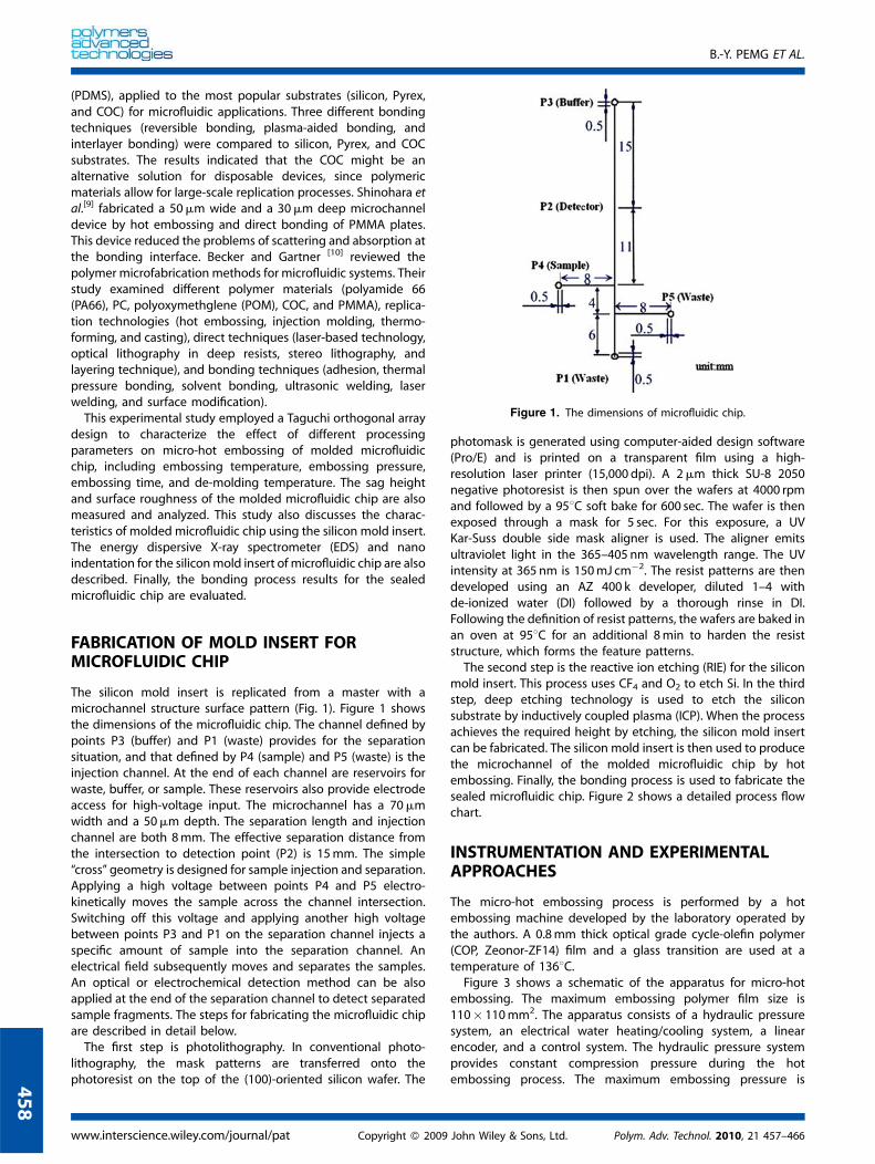
The silicon mold insert is replicated from a master with amicrochannel structure surface pattern (Fig. 1). Figure 1 showsthe dimensions of the microfluidic chip. The channel defined bypoints P3 (buffer) and P1 (waste) provides for the separationsituation, and that defined by P4 (sample) and P5 (waste) is theinjection channel. At the end of each channel are reservoirs forwaste, buffer, or sample. These reservoirs also provide electrodeaccess for high-voltage input. The microchannel has a 70mmwidth and a 50mm depth. The separation length and injectionchannel are both 8mm. The effective separation distance fromthe intersection to detection point (P2) is 15mm. The simple‘‘cross’’ geometry is designed for sample injection and separation.Applying a high voltage between points P4 and P5 electro-kinetically moves the sample across the channel intersection.Switching off this voltage and applying another high voltagebetween points P3 and P1 on the separation channel injects aspecific amount of sample into the separation channel. Anelectrical field subsequently moves and separates the samples.An optical or electrochemical detection method can be alsoapplied at the end of the separation channel to detect separatedsample fragments. The steps for fabricating the microfluidic chipare described in detail below.The first step is photolithography. In conventional photo-
lithography, the mask patterns are transferred onto thephotoresist on the top of the (100)-oriented silicon wafer. The
photomask is generated using computer-aided design software(Pro/E) and is printed on a transparent film using a high-resolution laser printer (15,000 dpi). A 2mm thick SU-8 2050negative photoresist is then spun over the wafers at 4000 rpmand followed by a 958C soft bake for 600 sec. The wafer is thenexposed through a mask for 5 sec. For this exposure, a UVKar-Suss double side mask aligner is used. The aligner emitsultraviolet light in the 365–405 nm wavelength range. The UVintensity at 365 nm is 150mJ cm�2. The resist patterns are thendeveloped using an AZ 400 k developer, diluted 1–4 withde-ionized water (DI) followed by a thorough rinse in DI.Following the definition of resist patterns, the wafers are baked inan oven at 958C for an additional 8min to harden the resiststructure, which forms the feature patterns.The second step is the reactive ion etching (RIE) for the silicon
mold insert. This process uses CF4 and O2 to etch Si. In the thirdstep, deep etching technology is used to etch the siliconsubstrate by inductively coupled plasma (ICP). When the processachieves the required height by etching, the silicon mold insertcan be fabricated. The silicon mold insert is then used to producethe microchannel of the molded microfluidic chip by hotembossing. Finally, the bonding process is used to fabricate thesealed microfluidic chip. Figure 2 shows a detailed process flowchart.
INSTRUMENTATION AND EXPERIMENTALAPPROACHES
The micro-hot embossing process is performed by a hotembossing machine developed by the laboratory operated bythe authors. A 0.8mm thick optical grade cycle-olefin polymer(COP, Zeonor-ZF14) film and a glass transition are used at atemperature of 1368C.Figure 3 shows a schematic of the apparatus for micro-hot
embossing. The maximum embossing polymer film size is110� 110mm2. The apparatus consists of a hydraulic pressuresystem, an electrical water heating/cooling system, a linearencoder, and a control system. The hydraulic pressure systemprovides constant compression pressure during the hotembossing process. The maximum embossing pressure is
Figure 1. The dimensions of microfluidic chip.
www.interscience.wiley.com/journal/pat Copyright � 2009 John Wiley & Sons, Ltd. Polym. Adv. Technol. 2010, 21 457–466
B.-Y. PEMG ET AL.
458
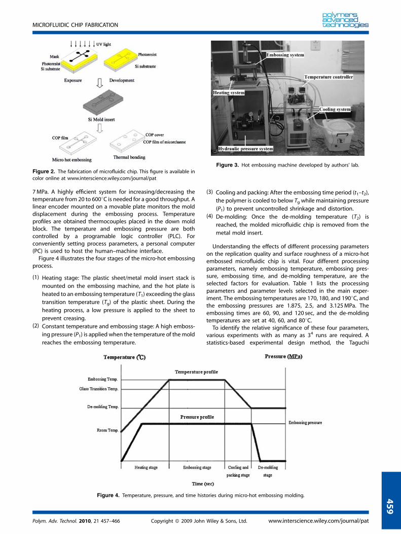
7MPa. A highly efficient system for increasing/decreasing thetemperature from 20 to 6008C is needed for a good throughput. Alinear encoder mounted on a movable plate monitors the molddisplacement during the embossing process. Temperatureprofiles are obtained thermocouples placed in the down moldblock. The temperature and embossing pressure are bothcontrolled by a programable logic controller (PLC). Forconveniently setting process parameters, a personal computer(PC) is used to host the human–machine interface.Figure 4 illustrates the four stages of the micro-hot embossing
process.
(1) Heating stage: The plastic sheet/metal mold insert stack is
mounted on the embossing machine, and the hot plate is
heated to an embossing temperature (T1) exceeding the glass
transition temperature (Tg) of the plastic sheet. During the
heating process, a low pressure is applied to the sheet to
prevent creasing.(2) Constant temperature and embossing stage: A high emboss-
ing pressure (P1) is applied when the temperature of themold
reaches the embossing temperature.
(3) Cooling and packing: After the embossing time period (t1–t2),
the polymer is cooled to below Tg while maintaining pressure
(P1) to prevent uncontrolled shrinkage and distortion.(4) De-molding: Once the de-molding temperature (T2) is
reached, the molded microfluidic chip is removed from the
metal mold insert.
Understanding the effects of different processing parameterson the replication quality and surface roughness of a micro-hotembossed microfluidic chip is vital. Four different processingparameters, namely embossing temperature, embossing pres-sure, embossing time, and de-molding temperature, are theselected factors for evaluation. Table 1 lists the processingparameters and parameter levels selected in the main exper-iment. The embossing temperatures are 170, 180, and 1908C, andthe embossing pressures are 1.875, 2.5, and 3.125MPa. Theembossing times are 60, 90, and 120 sec, and the de-moldingtemperatures are set at 40, 60, and 808C.To identify the relative significance of these four parameters,
various experiments with as many as 34 runs are required. Astatistics-based experimental design method, the Taguchi
Figure 2. The fabrication of microfluidic chip. This figure is available in
color online at www.interscience.wiley.com/journal/pat
Figure 4. Temperature, pressure, and time histories during micro-hot embossing molding.
Figure 3. Hot embossing machine developed by authors’ lab.
Polym. Adv. Technol. 2010, 21 457–466 Copyright � 2009 John Wiley & Sons, Ltd. www.interscience.wiley.com/journal/pat
MICROFLUIDIC CHIP FABRICATION
459
method,[11] is used to reduce the number of experimentalruns. Table 1 shows the levels of processing conditionsand the experimental array. The single-parameter methodis used to elucidate the surface roughness properties ofthe molded microfluidic chip for different processingparameters.Figure 5 indicates the pressure–temperature profile for thermal
bonding processing. The profile is similar to that of the hotembossing profile. The differences are that the maximumtemperature is 1–138C below Tg, and the maximum pressure is0.3–1.5MPa. The detailed illustrations are as follows:
(1) The mold insert and substrate are heated to 10–208C below
Tg, and the temperature distribution was uniformly improved.
In comparison with the hot embossing process, the keeping
time must be at least 5 min for an optimal thermal bonding
effect. The heating rate is 0.68C sec�1. In the second heating
stage, the mold insert and substrate are heated to 5–108Cbelow Tg. The heating rate is 0.1–0.48C sec�1. Simultaneously,
the substrate is pressed with increasing pressure at a rate of
0.01–0.02MPa sec�1. The maximum temperature is main-
tained for 5–7min. The maximum pressure is 0.3–1.5MPa.
The maintenance pressure must be controlled at an appro-
priate value (0.8–1.0MPa) to avoid producing an overly
shallow microchannel.(2) The pressure is decreased as the temperature is reduced
below glass transition temperature, and the cooling rate
should not be too fast (appropriate value is 0.4–0.58C sec�1).
1). As the temperature decreases to room temperature, the
de-molding procedure is performed.
Thermal bonding processing also uses the same machinedeveloped by this laboratory (Fig. 3).
Table 1. The L9 orthogonal array used in the main experiment
RunsEmbossing
temperature (8C)Embossing
pressure (MPa)Embossingtime (Sec)
De-moldingtemperature (8C)
1 1 (170) 1 (1.875) 1 (60) 1 (40)2 1 (170) 2 (2.500) 2 (90) 2 (60)3 1 (170) 3 (3.125) 3 (120) 3 (80)4 2 (180) 1 (1.875) 2 (90) 3 (80)5 2 (180) 2 (2.500) 3 (120) 1 (40)6 2 (180) 3 (3.125) 1 (60) 2 (60)7 3 (190) 1 (1.875) 3 (120) 2 (60)8 3 (190) 2 (2.500) 1 (60) 3 (80)9 3 (190) 3 (3.125) 2 (90) 1 (40)
Figure 5. Pressure–temperature profile for the thermal bonding.
www.interscience.wiley.com/journal/pat Copyright � 2009 John Wiley & Sons, Ltd. Polym. Adv. Technol. 2010, 21 457–466
B.-Y. PEMG ET AL.
460
EXPERIMENTAL RESULTS AND DISCUSSION
Mold insert
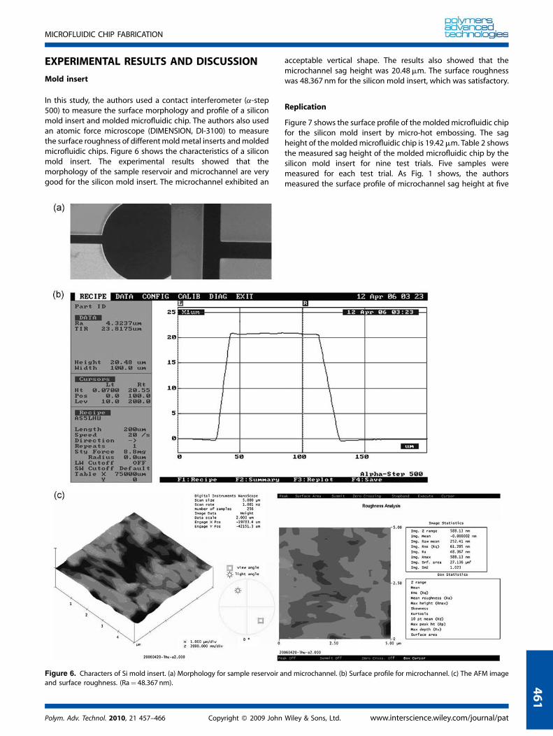
In this study, the authors used a contact interferometer (a-step500) to measure the surface morphology and profile of a siliconmold insert and molded microfluidic chip. The authors also usedan atomic force microscope (DIMENSION, DI-3100) to measurethe surface roughness of differentmoldmetal inserts andmoldedmicrofluidic chips. Figure 6 shows the characteristics of a siliconmold insert. The experimental results showed that themorphology of the sample reservoir and microchannel are verygood for the silicon mold insert. The microchannel exhibited an
acceptable vertical shape. The results also showed that themicrochannel sag height was 20.48mm. The surface roughnesswas 48.367 nm for the silicon mold insert, which was satisfactory.
Replication
Figure 7 shows the surface profile of the moldedmicrofluidic chipfor the silicon mold insert by micro-hot embossing. The sagheight of themoldedmicrofluidic chip is 19.42mm. Table 2 showsthe measured sag height of the molded microfluidic chip by thesilicon mold insert for nine test trials. Five samples weremeasured for each test trial. As Fig. 1 shows, the authorsmeasured the surface profile of microchannel sag height at five
Figure 6. Characters of Si mold insert. (a) Morphology for sample reservoir and microchannel. (b) Surface profile for microchannel. (c) The AFM image
and surface roughness. (Ra¼ 48.367 nm).
Polym. Adv. Technol. 2010, 21 457–466 Copyright � 2009 John Wiley & Sons, Ltd. www.interscience.wiley.com/journal/pat
MICROFLUIDIC CHIP FABRICATION
461
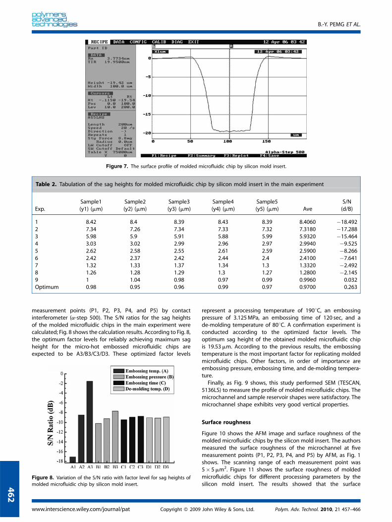
measurement points (P1, P2, P3, P4, and P5) by contactinterferometer (a-step 500). The S/N ratios for the sag heightsof the molded microfluidic chips in the main experiment werecalculated; Fig. 8 shows the calculation results. According to Fig. 8,the optimum factor levels for reliably achieving maximum sagheight for the micro-hot embossed microfluidic chips areexpected to be A3/B3/C3/D3. These optimized factor levels
represent a processing temperature of 1908C, an embossingpressure of 3.125MPa, an embossing time of 120 sec, and ade-molding temperature of 808C. A confirmation experiment isconducted according to the optimized factor levels. Theoptimum sag height of the obtained molded microfluidic chipis 19.53mm. According to the previous results, the embossingtemperature is the most important factor for replicating moldedmicrofluidic chips. Other factors, in order of importance areembossing pressure, embossing time, and de-molding tempera-ture.Finally, as Fig. 9 shows, this study performed SEM (TESCAN,
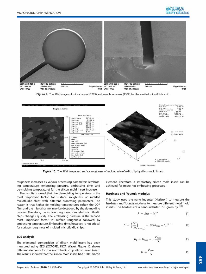
5136LS) to measure the profile of molded microfluidic chips. Themicrochannel and sample reservoir shapes were satisfactory. Themicrochannel shape exhibits very good vertical properties.
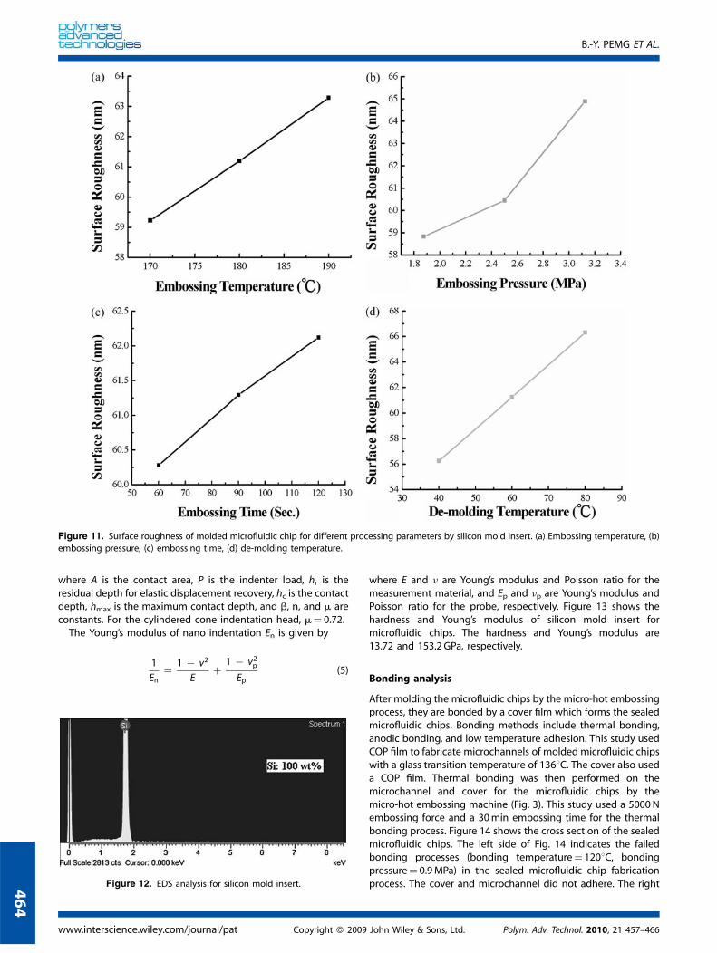
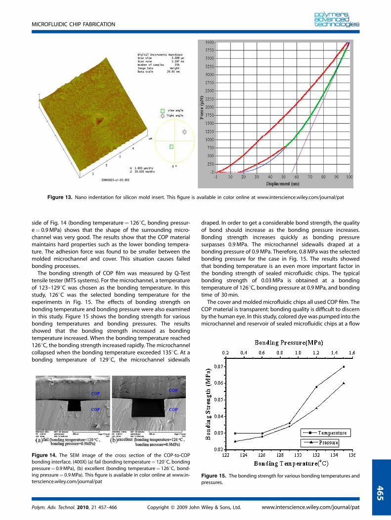
Surface roughness
Figure 10 shows the AFM image and surface roughness of themolded microfluidic chips by the silicon mold insert. The authorsmeasured the surface roughness of the microchannel at fivemeasurement points (P1, P2, P3, P4, and P5) by AFM, as Fig. 1shows. The scanning range of each measurement point was5� 5mm2. Figure 11 shows the surface roughness of moldedmicrofluidic chips for different processing parameters by thesilicon mold insert. The results showed that the surface
Figure 7. The surface profile of molded microfluidic chip by silicon mold insert.
Table 2. Tabulation of the sag heights for molded microfluidic chip by silicon mold insert in the main experiment
Exp.Sample1(y1) (mm)
Sample2(y2) (mm)
Sample3(y3) (mm)
Sample4(y4) (mm)
Sample5(y5) (mm) Ave
S/N(d/B)
1 8.42 8.4 8.39 8.43 8.39 8.4060 �18.4922 7.34 7.26 7.34 7.33 7.32 7.3180 �17.2883 5.98 5.9 5.91 5.88 5.99 5.9320 �15.4644 3.03 3.02 2.99 2.96 2.97 2.9940 �9.5255 2.62 2.58 2.55 2.61 2.59 2.5900 �8.2666 2.42 2.37 2.42 2.44 2.4 2.4100 �7.6417 1.32 1.33 1.37 1.34 1.3 1.3320 �2.4928 1.26 1.28 1.29 1.3 1.27 1.2800 �2.1459 1 1.04 0.98 0.97 0.99 0.9960 0.032Optimum 0.98 0.95 0.96 0.99 0.97 0.9700 0.263
Figure 8. Variation of the S/N ratio with factor level for sag heights of
molded microfluidic chip by silicon mold insert.
www.interscience.wiley.com/journal/pat Copyright � 2009 John Wiley & Sons, Ltd. Polym. Adv. Technol. 2010, 21 457–466
B.-Y. PEMG ET AL.
462
roughness increases as various processing parameters (emboss-ing temperature, embossing pressure, embossing time, andde-molding temperature) for the silicon mold insert increase.The results showed that the de-molding temperature is the
most important factor for surface roughness of moldedmicrofluidic chips with different processing parameters. Thereason is that higher de-molding temperatures soften the COPfilm, and the microchannel may be destroyed by the de-moldingprocess. Therefore, the surface roughness of molded microfluidicchips changes quickly. The embossing pressure is the secondmost important factor in surface roughness followed byembossing temperature. Embossing time, however, is not criticalfor surface roughness of molded microfluidic chips.
EDS analysis
The elemental composition of silicon mold insert has beenmeasured using EDS (OXFORD, INCA Wave). Figure 12 showsdifferent elements for the microfluidic chip silicon mold insert.The results showed that the silicon mold insert had 100% silicon
element. Therefore, a satisfactory silicon mold insert can beachieved for micro-hot embossing processes.
Hardness and Young’s modulus
This study used the nano indenter (Hysitron) to measure thehardness and Young’s modulus to measure different metal moldinserts. The hardness of a nano indenter H is given by [12]
P ¼ b h� hrð Þn (1)
S ¼ dP
dh
� �h¼hmax
¼ bn hmax � hrð Þn�1 (2)
hc ¼ hmax � mPmax
S(3)
H ¼ Pmax
S(4)
Figure 9. The SEM images of microchannel (200X) and sample reservoir (150X) for the molded microfluidic chip.
Figure 10. The AFM image and surface roughness of molded microfluidic chip by silicon mold insert.
Polym. Adv. Technol. 2010, 21 457–466 Copyright � 2009 John Wiley & Sons, Ltd. www.interscience.wiley.com/journal/pat
MICROFLUIDIC CHIP FABRICATION
463
where A is the contact area, P is the indenter load, hr is theresidual depth for elastic displacement recovery, hc is the contactdepth, hmax is the maximum contact depth, and b, n, and m areconstants. For the cylindered cone indentation head, m¼ 0.72.The Young’s modulus of nano indentation En is given by
1
En¼ 1 � v2
Eþ 1 � v2p
Ep(5)
where E and n are Young’s modulus and Poisson ratio for themeasurement material, and Ep and np are Young’s modulus andPoisson ratio for the probe, respectively. Figure 13 shows thehardness and Young’s modulus of silicon mold insert formicrofluidic chips. The hardness and Young’s modulus are13.72 and 153.2 GPa, respectively.
Bonding analysis
After molding the microfluidic chips by the micro-hot embossingprocess, they are bonded by a cover film which forms the sealedmicrofluidic chips. Bonding methods include thermal bonding,anodic bonding, and low temperature adhesion. This study usedCOP film to fabricate microchannels of molded microfluidic chipswith a glass transition temperature of 1368C. The cover also useda COP film. Thermal bonding was then performed on themicrochannel and cover for the microfluidic chips by themicro-hot embossing machine (Fig. 3). This study used a 5000Nembossing force and a 30min embossing time for the thermalbonding process. Figure 14 shows the cross section of the sealedmicrofluidic chips. The left side of Fig. 14 indicates the failedbonding processes (bonding temperature¼ 1208C, bondingpressure¼ 0.9MPa) in the sealed microfluidic chip fabricationprocess. The cover and microchannel did not adhere. The right
Figure 11. Surface roughness of molded microfluidic chip for different processing parameters by silicon mold insert. (a) Embossing temperature, (b)
embossing pressure, (c) embossing time, (d) de-molding temperature.
Figure 12. EDS analysis for silicon mold insert.
www.interscience.wiley.com/journal/pat Copyright � 2009 John Wiley & Sons, Ltd. Polym. Adv. Technol. 2010, 21 457–466
B.-Y. PEMG ET AL.
464
side of Fig. 14 (bonding temperature¼ 1268C, bonding pressur-e¼ 0.9MPa) shows that the shape of the surrounding micro-channel was very good. The results show that the COP materialmaintains hard properties such as the lower bonding tempera-ture. The adhesion force was found to be smaller between themolded microchannel and cover. This situation causes failedbonding processes.The bonding strength of COP film was measured by Q-Test
tensile tester (MTS systems). For the microchannel, a temperatureof 123–1298C was chosen as the bonding temperature. In thisstudy, 1268C was the selected bonding temperature for theexperiments in Fig. 15. The effects of bonding strength onbonding temperature and bonding pressure were also examinedin this study. Figure 15 shows the bonding strength for variousbonding temperatures and bonding pressures. The resultsshowed that the bonding strength increased as bondingtemperature increased. When the bonding temperature reached1268C, the bonding strength increased rapidly. The microchannelcollapsed when the bonding temperature exceeded 1358C. At abonding temperature of 1298C, the microchannel sidewalls
draped. In order to get a considerable bond strength, the qualityof bond should increase as the bonding pressure increases.Bonding strength increases quickly as bonding pressuresurpasses 0.9MPa. The microchannel sidewalls draped at abonding pressure of 0.9MPa. Therefore, 0.8MPa was the selectedbonding pressure for the case in Fig. 15. The results showedthat bonding temperature is an even more important factor inthe bonding strength of sealed microfluidic chips. The typicalbonding strength of 0.03MPa is obtained at a bondingtemperature of 1268C, bonding pressure at 0.9MPa, and bondingtime of 30min.The cover and molded microfluidic chips all used COP film. The
COP material is transparent: bonding quality is difficult to discernby the human eye. In this study, colored dye was pumped into themicrochannel and reservoir of sealed microfluidic chips at a flow
Figure 13. Nano indentation for silicon mold insert. This figure is available in color online at www.interscience.wiley.com/journal/pat
Figure 14. The SEM image of the cross section of the COP-to-COP
bonding interface. (400X) (a) fail (bonding temperature¼ 1208C, bondingpressure¼ 0.9MPa), (b) excellent (bonding temperature¼ 1268C, bond-ing pressure¼ 0.9MPa). This figure is available in color online at www.in-terscience.wiley.com/journal/pat
Figure 15. The bonding strength for various bonding temperatures and
pressures.
Polym. Adv. Technol. 2010, 21 457–466 Copyright � 2009 John Wiley & Sons, Ltd. www.interscience.wiley.com/journal/pat
MICROFLUIDIC CHIP FABRICATION
465
rate of 0.5mlmin�1. No leakage phenomenon occurred in themicrochannel or reservoir of the sealed microfluidic chips.
CONCLUSIONS
The findings of this study indicate that the replication and surfaceroughness of microfluidic chips are influenced by the siliconmoldinsert for micro-hot embossing. The results showed that siliconmold inserts are effective for replicating molded microfluidicchips. Embossing temperature is the most important factor forreplicating molded microfluidic chips on different processingparameters. De-molding temperature is the most importantfactor in the surface roughness of molded microfluidic chipsunder varying processing parameters. The experimental resultsalso indicated that the hardness of the silicon mold insert has agood value. The silicon mold insert must have low roughness andhigh hardness. Bonding temperature is the most important factorin the bonding strength of sealed microfluidic chips.
REFERENCES
[1] S. Y. Chou, P. R. Kraus, Microelectron. Eng. 1997, 35, 237–240.[2] L. J. Kricka, P. Fortina, N. J. Panaro, P. Wilding, G. A. Amigo, H. Becker,
Lab Chip. 2002, 2, 1–4.[3] J. Narasimhan, I. Papautsky, J. Micromech. Microeng. 2004, 14, 96–
103.[4] Y. Sun, Y. C. Kwok, N. T. Nguyon, J. Micromech. Microeng. 2006, 16,
1681–1688.[5] C. K. Fredrickson, Z. Xia, C. Das, R. Ferguson, F. T. Tarares, Z. H. Fan., J.
Microelectromechanical Sys. 2006, 15, 1060–1068.[6] N. S. Caneron, H. Roberge, T. Veres, S. C. Jakeway, H. J. Crabtree, Lab
Chip. 2006, 6, 936–941.[7] M. S. Cho, H. W. Lim, C. S. Lee, B. K. Cho, J. G. Park., Jpn. J. Appl. Phys.
2008, 47, 5215–5220.[8] M. Quaglio, G. Cauavese, E. Giuri, S. L. Marasso, D. Perrone, M.
Cocuzza, C. F. Pirri, J. Micromech. Microeng. 2008, 18, 055012.[9] H. Shinohara, J. Mizuno, S. Shoji, Jpn. J. Appl. Phys. 2007, 46,
3661–3664.[10] H. Becker, C. Gartner, Anal. Bioanal. Chem. 2008, 390, 89–111.[11] G. S. Peace, Taguchi Methods, Addison-Wesley, New York, 1993.[12] W. C. Oliver, G. M. Pharr, J. Mater. Res. 1992, 7, 1564–1583.
www.interscience.wiley.com/journal/pat Copyright � 2009 John Wiley & Sons, Ltd. Polym. Adv. Technol. 2010, 21 457–466
B.-Y. PEMG ET AL.
466