Embed Size (px)
Citation preview

Industrial Energy Efficiency Accelerator - Guide to the microelectronics sector The UK microelectronics sector uses more than 1,300 GWh of energy each year representing nearly 710,000 tonnes in carbon dioxide emissions. The energy consumed is required to create the clean working environment (40%), process tools plant (40%) and cleanroom utilities, such as process gas and ultra pure water (20%). While energy reduction of over 69% has been achieved over the last 10 years, there are opportunities to reduce these further.
Executive Summary The UK microelectronics sector uses more than 1,300 GWh of energy each year representing nearly 710,000
tonnes in carbon dioxide emissions. The three largest organisations account for approximately 25% of the total
energy consumption. There are 26 significant regional manufacturers that make up the UK industry.
According to a 2005 study by the International SEMATECH Manufacturing Initiative (ISMI) the global
semiconductor industry could save $500 million/year (industry wide) in energy costs through modest
improvements to tools and facilities1 . The UK contributed approximately 15% to this global figure
2 . Between
2006 and 2008 the UK microelectronics sector achieved a reduction of 500,000MWh/year in energy use. This is
equivalent to £2.65m reduction in the Climate Change Agreement levy3 .
The key productive component that is examined in this report is the wafer fabrication process used to create
semiconductors. This process relies heavily on an electrical energy intensive controlled environment and the use
of a complex manufacturing process. Both the fabrication and environmental components are supported by a vast
array of utilities.
The energy consumed in creating the clean working environment accounts for approximately 40% of the total
consumption of a manufacturing plant.
The “black box” of process tools plant also accounts for approximately 40% of the total consumption. Within the
tools environment the largest energy consumers are those associated with pumps and furnaces; with equipment
that often sitting in “idle” mode for large periods of time.
The remaining 20% is associated with cleanroom utilities i.e. process gas and ultra pure water etc.
1 International SEMATECH (ISMI) Sematech News, 2005
2 “UK semiconductor design evolves and grows stronger”, NMI, August 2006
3 „Sector and process overview”, by NMI on behalf of Carbon Trust, sourced from „Technical and Project Management
consultancy, Scope of Work”, 2010.
Microelectronics Sector Guide 2
During the course of this report we have observed that the Industry demonstrates a high level of activity in the
implementation of energy saving measures. An energy reduction of 69.3% has been achieved in the sector over
the last 10 years4 . Such measures are keenly supported by the trade association, the National Microelectronics
Institute, who believes a further 15% can be found through innovative solutions. Good progression has already
been made within the cleanroom environment particularly around the HVAC systems and their associated plant
and equipment.
The report has considered the process in detail to identify what opportunities also might be available. The
opportunities have been divided between good practice measures and Innovations. Both face common business
barriers in the form of proven technology and capital expenditure. These opportunities are summarised as:
Innovation:
Reverse Osmosis (RO) & Recovery Reverse Osmosis (RRO);
Electronic De-Ionisation (EDI);
De-ionised water reduction;
Best Practice
Light gauge overbend furnace elements;
Clean Dry Air (CDA);
On-site nitrogen (N2) gas generation.
Furnace vacuum insulation;
Stand-by options for load lock vacuum pumps;
Asset management and replacement plan for other vacuum pumps; and
High efficiency electric motors.
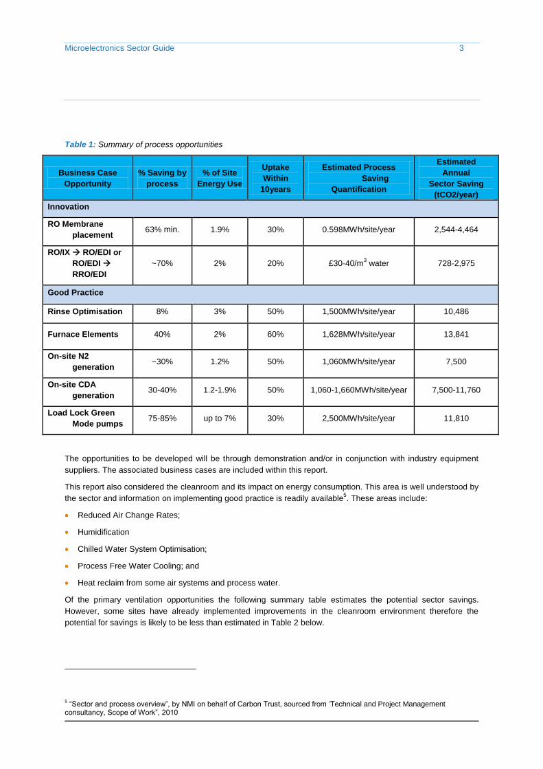
The following summary table was completed for the opportunities considered that offer the greatest business case
appeal which are estimated to achieve a sector wide reduction of 17-19% in energy use. Those not included in
the table yet listed above are opportunities already implemented, in part, across the microelectronics sector and
considered to be best practice opportunities with low return (CO2 and monetary) in comparison to those that are
described in more detail below.
4 Sector and process overview”, by NMI on behalf of Carbon Trust, sourced from „Technical and Project Management
consultancy, Scope of Work”, 2010.
Microelectronics Sector Guide 3
Table 1: Summary of process opportunities
Business Case
Opportunity
% Saving by
process
% of Site
Energy Use
Uptake
Within
10years
Estimated Process
Saving
Quantification
Estimated
Annual
Sector Saving
(tCO2/year)
Innovation
RO Membrane
placement 63% min. 1.9% 30% 0.598MWh/site/year 2,544-4,464
RO/IX RO/EDI or
RO/EDI
RRO/EDI
~70% 2% 20% £30-40/m3 water 728-2,975
Good Practice
Rinse Optimisation 8% 3% 50% 1,500MWh/site/year 10,486
Furnace Elements 40% 2% 60% 1,628MWh/site/year 13,841
On-site N2
generation ~30% 1.2% 50% 1,060MWh/site/year 7,500
On-site CDA
generation 30-40% 1.2-1.9% 50% 1,060-1,660MWh/site/year 7,500-11,760
Load Lock Green
Mode pumps 75-85% up to 7% 30% 2,500MWh/site/year 11,810
The opportunities to be developed will be through demonstration and/or in conjunction with industry equipment
suppliers. The associated business cases are included within this report.
This report also considered the cleanroom and its impact on energy consumption. This area is well understood by
the sector and information on implementing good practice is readily available5. These areas include:
Reduced Air Change Rates;
Humidification
Chilled Water System Optimisation;
Process Free Water Cooling; and
Heat reclaim from some air systems and process water.
Of the primary ventilation opportunities the following summary table estimates the potential sector savings.
However, some sites have already implemented improvements in the cleanroom environment therefore the
potential for savings is likely to be less than estimated in Table 2 below.
5 “Sector and process overview”, by NMI on behalf of Carbon Trust, sourced from „Technical and Project Management
consultancy, Scope of Work”, 2010

Microelectronics Sector Guide 4
Table 2: Summary of Facilities Opportunities
% process
saving
% of Site
Energy Use
Uptake within
10years
Annual Sector
Saving (tCO2)
Reduced cleanroom
airflows
24% 18% 80% 40,000
Mist Humidification 40% 18% 80% 35,000
Generic Application
There were a number of key observations that we have learned in this investigation that have a significant impact
upon the sector wide implementation of any opportunity including:
All Fab utilities and processes are interlinked;
The nature of the precise process means every site is unique and therefore single site data is not necessarily
industry representative;
Recently implemented changes related to energy savings often arise from alternative drivers such as cost
savings or yield improvement.
Such interdependencies are extremely complex, diverse and site specific. Whilst this report provides a reference
base for potential energy savings it is the individual sites and their own specific nature of operation that will
determine which of the opportunities listed have merit for that particular site.

Microelectronics Sector Guide 5
Table of contents Executive Summary ................................................................................................. 1
1 Introduction .......................................................................................................... 6
1.1 Report overview ................................................................................................................. 6
1.2 Background to Industrial Energy Efficiency Accelerator .................................................... 7
2 Sector overview ................................................................................................... 8
2.1 Background ........................................................................................................................ 8
2.2 Global ................................................................................................................................. 8
2.3 UK ...................................................................................................................................... 9
2.4 Trade associations ........................................................................................................... 10
2.5 Business drivers............................................................................................................... 10
2.6 Business barriers ............................................................................................................. 11
2.7 Engagement with the sector ............................................................................................ 11
2.8 Semiconductor manufacturing process ........................................................................... 13
2.9 Sector energy use ............................................................................................................ 17
3 Process energy use ........................................................................................... 21
3.1 General ............................................................................................................................ 21
3.2 Process opportunities ...................................................................................................... 23
3.3 Process summary ............................................................................................................ 36
4 Facilities ............................................................................................................. 38
4.1 Facilities areas ................................................................................................................. 38
4.2 Facilities energy use ........................................................................................................ 41
4.4 Facilities summary ........................................................................................................... 48
5 Opportunities ..................................................................................................... 51
5.1 Overview of opportunities ................................................................................................ 51
5.2 Process best practice opportunities ................................................................................. 52
5.3 Process innovation opportunities ..................................................................................... 55
5.4 Business cases ................................................................................................................ 57
6 Next steps .......................................................................................................... 60
Appendices ............................................................................................................. 62

Microelectronics Sector Guide 6
1 Introduction
1.1 Report overview
This report summarises the findings of the first stage of the Industrial Energy Efficiency Accelerator (IEEA) for the
microelectronics sector.
A description of the microelectronics sector in the UK and how the dominant product, wafer fabrication, is
manufactured is presented as an introduction to the possible areas where energy usage may be reduced.
Using data obtained from National Microelectronics Institute (NMI), The Carbon Trust and a number of
manufacturers within the sector, the energy consumption of the nominated plants in the UK has been analysed
and compared to the UK wide sector energy usage.
Energy use within a number of plant facilities (typically known as a „Fab‟) is presented to highlight the main
energy hotspots. These areas were then used as the focus when identifying potential energy saving options and
the data collection requirements for the pilot sites to be specified. Five established sites have been consulted for
detailed on-site investigation and information gathering in this study. These sites have been brought into the
project as key stakeholders and solution collaborators.
The sites were selected through consultation with the NMI and because they are representative of the industry
within the UK and demonstrate the diversity of the technologies in use throughout the sector.
All stakeholders recognise that the nature of this industry is extremely complex and bespoke in relation to facility
design and operation, equipment specification and process choice. It is also possible to have a product that can,
to all intents and purposes, achieve the same performance or capability but be from a different wafer design at
each individual manufacturing site.
The microelectronics industry is inherently sensitive to intellectual property and the commercial advantages, or
otherwise, of providing even seemingly generic information on energy use and process details.
The following should be considered when reading this report:
It is not possible to consider any one aspect of the operation of a wafer Fab facility in isolation. Utilities,
facilities, process and production are all interdependent activities;
No two wafer Fab facilities are the same. Even when the facilities appear to be producing the same product,
the process undertaken to produce that product has to be considered in isolation;
Process related energy savings are difficult to quantify due to additional industry drivers such as cost of
product, time to marketplace and yield which are equally important and inherently interlinked in terms of
impact and solution success.

Microelectronics Sector Guide 7
The implementation of even “good practices” maybe impeded by some other fabrication process that we have not
inter-linked. Therefore, as with all of the opportunities highlighted in this report even best practice will ultimately
be subject to its own due diligence on quality and throughput.
1.2 Background to Industrial Energy Efficiency Accelerator
The IEEA was created to deliver a step change reduction in industrial process emissions by accelerating
innovation in process control and the uptake of low carbon technologies. Industry is responsible for 25% of the
UK‟s total carbon dioxide (CO2) emissions. The Carbon Trust‟s experience supports the view of the Committee
on Climate Change, which indicated that savings of 4-6mtCO2 (up to 4% of current emissions) should be
realistically achievable in industry with appropriate interventions6.
By demonstrating to organisations their energy use and the available opportunities to address this, it is possible
to accelerate, increase impact and achieve far greater savings than the current policy targets can achieve alone.
In 2008 approximately 151,000tCO2 worth of emissions allowances were sold through inter-sector trading, with
accounts managed by the NMI. These allowances were sold due to an over performance against Climate
Change Levy targets, primarily due to increased throughput from an accepted benchmark. However due to the
industry‟s continued success of emission reductions in recent years a further 9% reduction in the sector‟s
allowances was set for the next reporting period. An industry workshop hosted by the NMI in June 2010
concluded that as much as 15% more energy reductions could be achieved through the majority of these savings
would require the introduction of innovative processes or equipment improvements. Innovative thinking is the key
to the success of the IEEA programme, an approach it was specifically setup to embrace in the goal to accelerate
a low carbon economy.
The Carbon Trust‟s historical approach to working with industry was through advice, activities, supporting
companies to reduce their carbon emissions. This did not look in-depth at sector-specific processes. Industries
frequently cite as a reason for not implementing survey recommendations, that they do not address the majority
of their energy use. Between 50% and 90% of a site‟s energy consumption could typically be used by a sector-
specific manufacturing process.
The IEEA approach focuses on identifying and addressing the barriers preventing industries from improving the
efficiency of their processes. There are three stages to the approach of which this study is related to Stage 1.
Figure 1: IEEA Project Stages
Since 2009, the IEEA work has worked in fourteen industry sectors from asphalt suppliers to bakeries, dairy
industry to microelectronics in order to identify innovative energy, carbon and cost savings in industrial
manufacturing processes savings typically averaging 29%.
6 Committee on Climate Change Report, December 2008

Microelectronics Sector Guide 8
2 Sector overview
This section offers a brief description of the Microelectronics sector in the UK, describing the wafer and
semiconductor manufacturing process as used throughout the sector.
Where possible, key energy performance statistics have been included as well as discussions on technological
changes that have already been introduced in the sector.
2.1 Background
The microelectronics manufacturing and semiconductor device fabrication industry manufactures micro or nano
integrated circuits for use in many of today‟s consumer electrical goods including personal computers and
communications devices. Consumer desire to have smaller, faster and better performing products drives the
industry towards constant development.
The most common type of semiconductor device produced is the integrated circuit (IC), which accounts for
roughly 85% of semiconductor production today. The remaining 15% is typically discrete devices (i.e. single
circuit element e.g. transistor, diode). The industry commonly refers to the finished device as an integrated circuit,
IC, chip or microchip. This report uses the term interchangeably. A finished IC consists of a wafer substrate on
which thin (~0.1 micron) silicon layers are added, each with their own specific circuiting, to create an integrated
circuit capable of performing a certain function or functions.
Semiconductor fabrication occurs in a highly engineered environment where the temperature, humidity and
contaminant content are controlled within very tight constraints to ensure product quality.
2.2 Global
The global semiconductor industry is currently worth $300 billion and expected to reach $314billion in 20117 . It
was affected by the global recession but is currently growing again in record numbers.
The largest companies within the semiconductor industry are listed below:
7 Study completed by Gartner in 2010, summary accessed from www.zdnetasia.com

Microelectronics Sector Guide 9
Figure 2: Top 10 Semiconductor Suppliers in Q1 2010 – Data sourced from iSuppli.com
Figure 3: Percentage of World Semiconductor sales – Source: WSTS
2.3 UK
Considering the data presented in section 2.2, microelectronics manufacturing within the UK is relatively small in
comparison to the global market. There are currently 28 semiconductor manufacturing facilities in the UK;
however the National Microelectronics Institute (NMI) continues to report a significant decline in manufacturing
over recent years.
Significantly, some of the biggest and most advanced sites have recently closed (NEC, Atmel NTS and
Freescale). Several smaller sites have also closed whilst others have changed ownership. Approximately 80% of
the semiconductor companies within the UK are foreign owned.
Microelectronics Sector Guide 10
The major products and product groupings manufactured by the sector are:
Semiconductor devices and electronic assemblies accounting for 92% of energy use
Substrates (wafer manufacture) accounting for 8% of energy use
These proportions have shifted to 90%/10% in 2008. The NMI expects the spread of product types to remain
about the same over the coming years, however with the recent closure of Freescale (a devices and assembly
manufacturer) the proportion of wafer energy consumption is expected to increase to 12% of the sector
consumption8 .
Despite the decline in manufacturing, the intellectual knowledge within the UK is a key selling point and a driver
for the industry.
As of 2008, 17 of the top 25 global semiconductor companies had R&D facilities within the UK.
Due to the constant focus on product development, companies invest large sums of money into R&D. This can
sometimes be as much as 50% of profits being reinvested into research. These R&D functions are currently still
carried out in the US and Europe although there is potential that this may move to Asia along with the production.
The cost of developing new devices and the complexity are such that no single company can afford to do this
independently or have the intellectual capability to succeed. Much collaboration is therefore made between
competing companies in research.
2.4 Trade associations
The semiconductor industry is represented in the UK by the Trade Association:
NMI – National Microelectronics Institute
Internationally there are a number of associations within the industry including:
SEMI (Semiconductor Equipment and Materials International) primarily in the US though Europe and Asia is
also represented in regional SEMI groups; and
SIA (Semiconductor Industry Association) in the US.
As mentioned in the introduction, the industry is typically very guarded about intellectual property. This includes
the trade associations and possible benefits from an international collaboration in industry improvements. This
report includes international findings and solutions but has primarily focussed on UK production and the NMI‟s
capabilities and remit.
2.5 Business drivers
Through discussions held at a sector workshop in June 2010 it was clear that the sector is very conscious of
energy consumption and can identify active progress to improve energy efficiency. The high level of awareness
and activity is typically driven by:
The requirement to comply with current and future legislation;
The need to remain competitive internationally by cutting costs and improving financial efficiency; and
The core values of the organisations and a desire to promote the reputation of the organisation.
8 National Microelectronics Institute, sourced from “Technical and Project Management Consultancy: Scope of Work.
Microelectronics Manufacturing”, Carbon Trust, 2010

Microelectronics Sector Guide 11
There was evidence of active energy management and reduction taking place in the sector. Review and
implementation -- amounting to significant investment value -- of energy saving ideas takes place as part of a
continuous improvement process. Significant improvements and savings have been made within the sector.
Some of the areas that have been identified will be summarised later in this report.
Energy is integral to the sector operation in terms of yield and quality due to the complex and highly controlled
processes required. These drivers lead to energy, and therefore carbon efficiency, being of increasing interest to
the sector.
2.6 Business barriers
By engaging with the sector, key barriers to implementing innovations were identified. These are summarised
below and have been considered as part of the evaluation of opportunities which are discussed in Section 5.
a) Product quality – any innovation impacting on a specific area of the process may appear to have a net
benefit on its own validity. However, the Fab setups are such that every process element is impacted by the
change of another. The wider implications of any suggested change have to be considered before
promoting a particular opportunity. This is discussed in more detail in Section 3.
b) Business Cases – the implementation of new innovations will need to have a good return on investment. A
payback of less than one year is typically cited based upon our observations and discussions with the host
sites. Therefore, it will be of paramount importance to deliver innovative improvements that can deliver the
required financial benefits within the payback criteria or via a long term investment plan planned within
individual Fabs that would allow a longer payback to be permitted.
c) Cost – Being a high-value sector innovation usually requires high capital to implement a step-change. The
impacts and implementation costs coupled with the high quality standards within the industry makes most
changes a costly exercise in this sector.
d) Proven technology – the sector has previously implemented energy saving innovations, most notably in
the utilities areas of Fabs. The implementation of revised facility techniques has been undertaken but the
approach to this is very cautious and involves considerable qualification time periods where the change is
approved by all stakeholders involved (e.g. customers, regulatory bodies etc.).
Typically alterations in process technology are not readily embraced as readily due to immediate impacts on
quality and throughput, although opportunities are known to exist if proven to be cost effective.
Implementation of any revised process technique is likely to be undertaken with a greater amount of caution
and time and not without a detailed due diligence being undertaken at the site.
e) Asset Lifetime – Equipment turnover in the sector is very low with most items replaced only when a failure
is completely uneconomical to repair (typically 25-30 years). This leads to long time periods for asset
replacement and for Fabs to benefit from technology improvements introduced by manufacturers.
Additionally, much of the equipment used is expensive making payback periods too long for most
businesses. The second-hand market, which provides overhauled though old equipment, is much cheaper
which supports the drive in production continuity rather than energy saving improvements. When
implementing new equipment with technology enhancements, the reduction in energy consumption often
becomes insignificant if compared to the capital invested when considering individual business cases.
2.7 Engagement with the sector
For the compilation of this report 5 host sites have been actively consulted. During the preparation of this report
each site was visited and engaged with in order to understand their process, energy usage and potentials for
energy savings.

Microelectronics Sector Guide 12
During the course of the investigation three workshops were facilitated. This was done to discuss the various
elements of the investigation source ideas for innovation and get agreement for areas of exploration. These were
delivered:
In June 2010 to introduce the project and to gain, from the industry members, ideas for investigation. This
lead to a list of 101 energy saving ideas that were refined to key areas.
In October 2010 to present on the potential opportunities within the Cleanroom environment and areas for
future consideration into the Process element.
In March 2011 to present on the potential opportunities identified in the Process element and to establish next
steps.
Five were selected for further investigation after consultation with the NMI and because they are considered to be
a representative cross-section of the industry within the UK and the technologies in use through the sector. For
the sake of confidentiality, we are unable to name them here.
Table 3 below presents a summary of 4 of the sites visited and their core data. The sites have indicated that
anonymity was preferred in this study and therefore, we have referred to the sites numerically.
Table 3: Site data
Site 1 Site 2 Site 3 Site 4
Employees 340 1,600 unknown unknown
Hours 24/7 24/7 unknown 24/5
Products Discrete
Devices, ICs,
Hard drives 6 & 8” wafers ICs, Bipolar
Wafer Size 4 & 6” 6 & 8” 6 & 8” 4, 5 & 6”
Clean Room Size 3,000m² unknown unknown 9000m²
Clean Room Grade 10 – not
classified
100 – not
classified
100 – not
classified
10 – not
classified
Annual Electrical kWh 14,655,000 77,250,000 34,283,575 32,729,200
Annual Gas kWh 4,714,000 unknown unknown 15,500,000
These sites represent approximately 12% of the UK sector‟s energy use. The sites are typically components of a
larger, multi-facility, corporation and the data above represents the UK fabrication facility for each organisation.
The sites are typically linked to a sister site located somewhere else in the World, most notably Asia and US.
Distribution of the end product is either direct to industry clients or to the sister site for further fabrication.
These sites manufactured a variety of products and were involved in different stages of production from wafer
manufacture through to chip manufacturing and packaging.
The products included:
Wafer substrate Discrete Devices
Integrated Circuits Hard drives
Bipolar Transistors MOSFET
Diodes

Microelectronics Sector Guide 13
The sites also manufactured a variety of different wafer sizes including:
4” (declining) 6” (UK industry standard)
5” (declining) 8” (future trend in UK)
The majority of the sites were operating 24 hours a day, in shift patterns, and between 5- 7 days per week. The
operating periods are reflective of a high product demand that is currently prevalent in the industry. Most sites
noted that production has been increasing over the last few years through an increase in demand but that the
demand can be cyclic.
2.8 Semiconductor manufacturing process
Semiconductor device fabrication is the process used to manufacture integrated circuits. The process is a
complex sequence of photographic and chemical processing steps whereby electronic circuits are gradually
created on a wafer made of pure semiconducting material. From the raw material to completion can involve up to
500 steps and can take weeks to complete.
Figure 4: Process Overview
The overall process is illustrated within the diagram above and described in more detail within the sections and
diagrams below.
2.8.1 Wafer manufacture
The fabrication process starts with the preparation of wafers. Wafers are typically high purity silicon (99.9999%
pure) grown into mono crystalline cylindrical ingots, known as boules. An ingot is typically 100kg.
Integrated circuits are essentially linear, that is they are formed on the surface of the silicon so as to maximise
the surface area of silicon. The ingots/ boules are sliced into thin discs or wafers using a diamond saw or wire
saw.
The thickness of the wafers is a function of their diameter. The main criterion that determines their thickness is
the requirement to be sufficiently robust to ensure flatness across the surface, above all else, to minimise difficult
and expensive planarisation steps. As an example 300mm diameter wafers are typically 0.775 mm thick. The
preparation of wafers from an ingot involves a series of operations that typically take place in a light industrial
environment with the latter stages being carried out in a cleanroom.
The slicing of the ingot is typically carried out using a wire saw or diamond saw. Wire saws cut multiple slices
simultaneously. After slicing, the surfaces of the wafers are lapped using abrasive slurry until the wafers are flat
to within about 2μm. An etching process is carried out to remove crystal damage that may occur during the

Microelectronics Sector Guide 14
lapping process. Finally after etching the wafers are polished using a chemical / mechanical process that
smoothes the uneven surface left from previous processes and makes the wafer flat and smooth enough to
support optical photolithography.
2.8.2 Insulating
In order to protect the silicon substrate and to form transistor gates, a thin layer of silicon dioxide (SiO2) is formed
over the silicon wafer. This is typically done by exposing the wafer to high temperatures (900-1200°C) in a
furnace.
2.8.3 Placing
This is the first step in the processing of a raw wafer into semiconductor device. It involves the growth of a high
purity and defect free monocrystalline layer onto the surface of the substrate. This process is carried out in a
diffusion furnace heated to around 1,100°C and takes between 4 and 14 hours. The high temperature required
within the furnace and the duration of the process means that this is most energy intensive process of the various
activities carried out in the device fabrication process. This process is also known as epitaxy.
2.8.4 Patterning
Following this placing step the wafer is then ready for photolithography. The wafer is coated with a layer of photo
resist using a spin coating process. The photo resist-coated wafer is then baked for a short time (30 to 60
seconds) to drive off excess photo resist solvent, typically at 90 - 100 °C.
After baking, a mask is applied to the wafer and the photo resist is exposed to a pattern of intense light. Optical
lithography typically uses ultraviolet light. Positive photo resist, the most common type, becomes soluble in the
basic developer when exposed; exposed negative photo resist becomes insoluble in the (organic) developer.
This chemical change allows some of the photo resist to be removed by a special solution, called "developer" by
analogy with photographic developer.
The resulting wafer is then "hard-baked". The hard bake solidifies the remaining photo resist, to make a more
durable protecting layer in future ion implantation, wet chemical etching, or plasma etching.
2.8.5 Removing
In etching, a liquid ("wet") or plasma ("dry") chemical agent removes the uppermost layer of the substrate in the
areas that are not protected by photo resist. In semiconductor fabrication, dry etching techniques are generally
used, as they are more accurate and avoid significant undercutting of the photo resist pattern. This is essential
when the width of the features to be defined is similar to or less than the thickness of the material being etched
When a layer of photo resist is no longer needed, it is removed from the substrate. This usually requires a liquid
"resist stripper", which chemically alters the resist so that it no longer adheres to the substrate. Alternatively,
photo resist may be removed by a plasma containing oxygen, which oxidizes it. This process is called ashing,
and resembles dry etching.
2.8.6 Implanting
The electrical properties of selected areas of the developing device are changed by implanting energised ions
(dopants) in the form of specific impurities into the areas not protected by photo-resist or other layers. These
basic steps are repeated for additional layers of silicon, glass and aluminium
Implant is via diffusion or ion implantation. Diffusion is carried out in a furnace with a flow of gas running over the
wafers. The process is not selective so the photo resist and patterning need to be done before this step. Ion
implantation is different from diffusion in that ion implantation shoots the desired dopant ions into the wafer. The
disadvantage of ion implantation is that wafers have to be processed one at a time while a diffusion chamber can
handle many wafers simultaneously.

Microelectronics Sector Guide 15
Implant is followed by an annealing process which repairs the damage caused to the wafers. This process
involves heating to allow the crystal lattice structure to repair itself.
2.8.7 Interconnecting
The finished wafer is an intricate sandwich of n type and p type silicon with insulating layers of glass and silicon
nitride. All other circuit components are constructed during the first few masking steps and the following masking
steps connect the components together. An insulating layer of glass is deposited and a contact mask is used to
define the contact points of each of the circuit elements. After the contact windows are etched the entire wafer is
covered with a thin layer of aluminium. The metal mask is used to define an aluminium layer and therefore
leaving a network of metal connections. The entire wafer is then covered with an insulating layer of glass and
silicon nitride to protect it from contamination during assembly. The final mask and passivation etch removes the
passivation material from the bonding pads which are used to electrically complete the circuit.
2.8.8 Packaging
While still on the wafer, each device is tested and functional and non-functional devices are identified. Non-
functional wafers, i.e. defects, are then re-circulated back into the process to rectify the defects. The amount of
recirculation impacts on the product “moves” i.e. throughput, at the facility which is a key performance indicator of
a Fab plant.
Following a satisfactory test the wafer is then ready for cutting into individual chips and assembly / packaging.
Figure 5 below is a graphical description of the typical stages employed in manufacturing a semiconductor
device.

Microelectronics Sector Guide 16
Figure 5: Typical steps involved in manufacturing a device

Microelectronics Sector Guide 17
2.9 Sector energy use
This section introduces the site wide energy consumption breakdown within a Fab facility.
2.9.1 General
The primary energy consuming activities within the sector fall into three general categories:
Table 4: Energy use in the microelectronics sector
Category Energy Split
Facilities / Cleanrooms 40%
Utilities (compressed air etc.) 20%
Process Tools 40%
Irrespective of product group or energy use in process tools, approximately 60-70% of total energy is used in
facilitating the clean room i.e. maintaining temperature and humidity conditions and providing utilities within the
manufacturing zone. The visits to the host sites and the resulting acquisition of energy data has indicated that the
majority of the energy efficiency savings, which have been implemented to date, have been focussed within the
utilities/facilities areas.
Energy consumed by the process tools has remained relatively constant (proportional to production output).
Energy savings achieved in the Process Tools have not necessarily been recorded as these “shop-floor tweaks”
usually reflect quality and/or throughput improvements with energy savings being very much of secondary
interest. However, due to increasing utilities costs, energy savings are gaining significance in the implementation
of changes to the process.
The following charts illustrate this trend indicating the step increase in the proportion of electrical energy
consumed by the process tools as part of the total site energy consumption.
Figure 6 Chart of electrical load distribution trends in recent years
The final chart is based on the current trend continuing, with process tools energy consumption remaining static
and predicts a 50/50 ratio. The rate of change, in this trend, is likely to decrease as the lower cost/ease of
implementation opportunities are implemented.
The charts above are averaged across a number of enterprises and although it is indicative of the sector the
energy split within a particular site is clearly a function of the balance of activities and the site location. For the
sites visited the split varied from 40% process/60% facilities and utilities to 55% process/45% facilities and
utilities.
Microelectronics Sector Guide 18
The information presented is consistent with UK and international benchmarking. For example, according to the
World Semiconductor Council (WSC), the energy needed to run process equipment and tools accounts for up to
40-50% of the total energy consumption in a semiconductor facility.
It should be noted that this data will vary across the globe due to the climatic influences on Fab humidification
levels. For example, a Fab in the UK will only see a high humidification demand for a short period of time in
summer months whereas a Fab in Asia will have a high, all-year round humidification requirement. The figures
quoted are a generic average across worldwide semiconductor manufacturers.
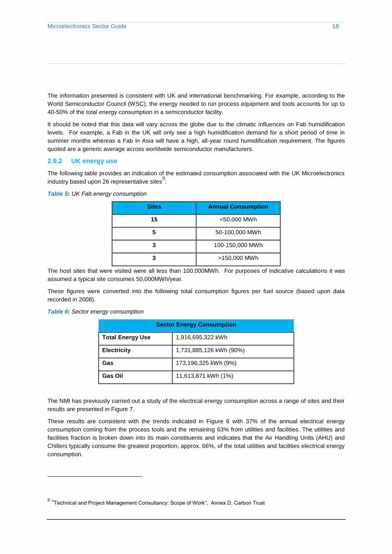
2.9.2 UK energy use
The following table provides an indication of the estimated consumption associated with the UK Microelectronics
industry based upon 26 representative sites9:
Table 5: UK Fab energy consumption
Sites Annual Consumption
15 <50,000 MWh
5 50-100,000 MWh
3 100-150,000 MWh
3 >150,000 MWh
The host sites that were visited were all less than 100,000MWh. For purposes of indicative calculations it was
assumed a typical site consumes 50,000MWh/year.
These figures were converted into the following total consumption figures per fuel source (based upon data
recorded in 2008).
Table 6: Sector energy consumption
Sector Energy Consumption
Total Energy Use 1,916,695,322 kWh
Electricity 1,731,885,126 kWh (90%)
Gas 173,196,325 kWh (9%)
Gas Oil 11,613,871 kWh (1%)
The NMI has previously carried out a study of the electrical energy consumption across a range of sites and their
results are presented in Figure 7.
These results are consistent with the trends indicated in Figure 6 with 37% of the annual electrical energy
consumption coming from the process tools and the remaining 63% from utilities and facilities. The utilities and
facilities fraction is broken down into its main constituents and indicates that the Air Handling Units (AHU) and
Chillers typically consume the greatest proportion, approx. 66%, of the total utilities and facilities electrical energy
consumption.
9 “Technical and Project Management Consultancy: Scope of Work”, Annex D, Carbon Trust
Microelectronics Sector Guide 19
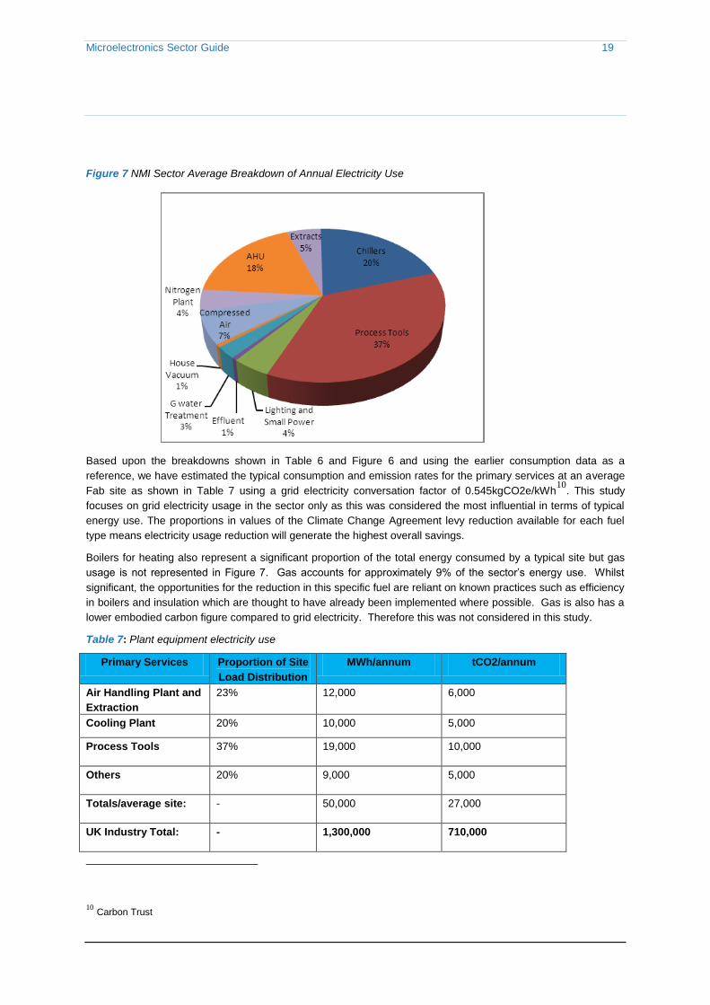
Figure 7 NMI Sector Average Breakdown of Annual Electricity Use
Based upon the breakdowns shown in Table 6 and Figure 6 and using the earlier consumption data as a
reference, we have estimated the typical consumption and emission rates for the primary services at an average
Fab site as shown in Table 7 using a grid electricity conversation factor of 0.545kgCO2e/kWh10
. This study
focuses on grid electricity usage in the sector only as this was considered the most influential in terms of typical
energy use. The proportions in values of the Climate Change Agreement levy reduction available for each fuel
type means electricity usage reduction will generate the highest overall savings.
Boilers for heating also represent a significant proportion of the total energy consumed by a typical site but gas
usage is not represented in Figure 7. Gas accounts for approximately 9% of the sector‟s energy use. Whilst
significant, the opportunities for the reduction in this specific fuel are reliant on known practices such as efficiency
in boilers and insulation which are thought to have already been implemented where possible. Gas is also has a
lower embodied carbon figure compared to grid electricity. Therefore this was not considered in this study.
Table 7: Plant equipment electricity use
Primary Services Proportion of Site
Load Distribution
MWh/annum tCO2/annum
Air Handling Plant and
Extraction
23% 12,000 6,000
Cooling Plant 20% 10,000 5,000
Process Tools 37% 19,000 10,000
Others 20% 9,000 5,000
Totals/average site: - 50,000 27,000
UK Industry Total: - 1,300,000 710,000
10
Carbon Trust
Microelectronics Sector Guide 20
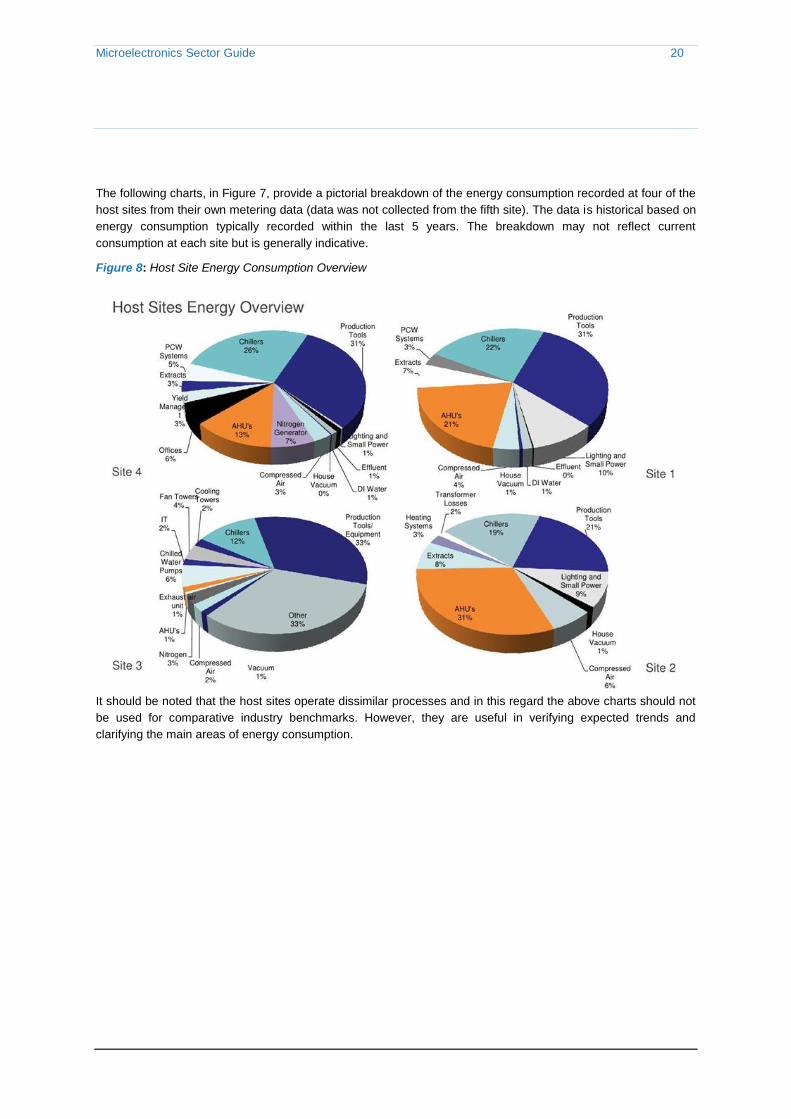
The following charts, in Figure 7, provide a pictorial breakdown of the energy consumption recorded at four of the
host sites from their own metering data (data was not collected from the fifth site). The data is historical based on
energy consumption typically recorded within the last 5 years. The breakdown may not reflect current
consumption at each site but is generally indicative.
Figure 8: Host Site Energy Consumption Overview
It should be noted that the host sites operate dissimilar processes and in this regard the above charts should not
be used for comparative industry benchmarks. However, they are useful in verifying expected trends and
clarifying the main areas of energy consumption.

Microelectronics Sector Guide 21
3 Process energy use
The following section reviews energy consumption across the processes i.e. process tools, within a Fab facility.
3.1 General
The following graphic indicates the various processes, which were described in Section 2, and the external input
that is required to complete the process. The external input can be in the form of water (or other chemical),
electrical input power to energise equipment used in the process (i.e. pumps etc.) and gases (i.e. nitrogen, clean
dry air etc.), that maybe used as an agent in the completion of the process.
Figure 9: Process Energy Inputs
The energy used across the process spectrum can be approximately distributed as follows:
Pumps – 50-60%: a Fab facility can contain up to 600 pumps in the process tooling, depending on output
capacity.
Heaters – 20-30%: associated with heating elements within furnaces
Other - 10-25%: comprises of items such as cleaning machines, automated interconnection machines etc.

Microelectronics Sector Guide 22
Of the process energy used in a Fab, the consumptions have been distributed across the typical processes in
Figure 10 below.
Figure 10: Typical Process Energy Use
The processes implemented by the Fab can be reliant on some or all of the following variables:
Product output quantities;
Product specification;
Product variety;
Customer requirements/contractual agreements; and
Utilities available at the site.
Discussions with host sites have established that, to date, process tools (i.e. machines) energy savings have
been restricted or at least difficult to quantify. Reasons for this are noted as follows:
There is general resistance from production departments to changing tool operating parameters. The focus of
the production team is quality and output. Changes to tool operating parameters have the potential to impact
on both quality and output. They also involve production downtime together with the need to go through a
recertification/ qualification process to ensure that the process achieves the required output and quality.
Tool energy consumption is not a primary consideration when procurement of new tools is being considered.
Several of the sites visited identified that they procure partly used equipment. In this situation the choice of
equipment is limited and as such their ability to influence tool manufacturers is also limited.
Although progress in reducing process tool energy is advancing, albeit at a slower rate than the reduction in
utilities/facilities energy, it was observed some progress has achieved savings through the following:
Utilising energy monitoring software on their process tools to better understand their usage; and

Microelectronics Sector Guide 23
Switching off a cryo compressor associated with one specific process tool. The compressor was only needed
for a single step in the process but yet had been running 24/7.
These observations were site specific but are indicative of sector focus increasing in the process tools area.
From our preliminary observations and review of the process tools, and the way we understand how they are
operated, the following headlines are noted:
The process energy demand profile is relatively flat. Much of the equipment operates continuously with a
relatively small difference between demand whilst idling and the full load demand. Ancillary equipment
associated with process tools, such as cryogenic pumps are also required to operate continuously; and
For most sites visited a significant proportion of the energy consumed by process tools is used within the
furnaces i.e. heating elements, associated vacuum pumps and ancillaries.
As an example, for Site 3, a site highly reliant on the epitaxy process, the reactor furnaces accounted for
approximately 50% of process tool energy consumption. High energy use associated with reactors is
characterised by the requirement for the equipment to operate continuously at elevated temperatures even when
the furnace is not in use.
3.2 Process opportunities
From the process energy use breakdown and knowledge of the processes and their associated equipment it has
been possible to categorise areas of opportunities that offer potential to reduce energy. We have divided the
opportunities into the following primary consumer categories and presented in Table 8:
Water use;
Furnaces;
Pumps; and
Compressed Gases
Table 8: Process Categories
Process Element Water Use Furnaces Pumps Compressed Gas
Wafer Manufacture √ √
Insulating √ √
Placing √ √ √
Patterning/Lithography √ √ √ √
Removing/Etching √ √ √ √
Implanting/Diffusion √ √ √
Interconnecting √ √
Packaging √ √
Cleaning √ √
Microelectronics Sector Guide 24
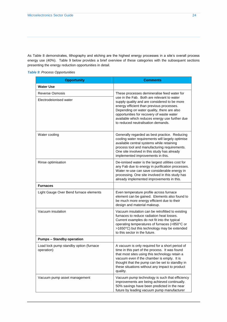
As Table 8 demonstrates, lithography and etching are the highest energy processes in a site‟s overall process
energy use (40%). Table 9 below provides a brief overview of these categories with the subsequent sections
presenting the energy reduction opportunities in detail.
Table 9: Process Opportunities
Opportunity Comments
Water Use
Reverse Osmosis These processes demineralise feed water for
use in the Fab. Both are relevant to water
supply quality and are considered to be more
energy efficient than previous processes.
Depending on water quality, there are also
opportunities for recovery of waste water
available which reduces energy use further due
to reduced neutralisation demands.
Electrodeionised water
Water cooling Generally regarded as best practice. Reducing
cooling water requirements will largely optimise
available central systems while retaining
process tool and manufacturing requirements.
One site involved in this study has already
implemented improvements in this.
Rinse optimisation De-ionised water is the largest utilities cost for
any Fab due to energy in purification processes.
Water re-use can save considerable energy in
processing. One site involved in this study has
already implemented improvements in this.
Furnaces
Light Gauge Over Bend furnace elements Even temperature profile across furnace
element can be gained. Elements also found to
be much more energy efficient due to their
design and material makeup.
Vacuum insulation Vacuum insulation can be retrofitted to existing
furnaces to reduce radiation heat losses.
Current examples do not fit into the typical
operating temperatures of furnaces (<850°C or
>1650°C) but this technology may be extended
to this sector in the future.
Pumps – Standby operation
Load lock pump standby option (furnace
operation)
A vacuum is only required for a short period of
time in this part of the process. It was found
that most sites using this technology retain a
vacuum even if the chamber is empty. It is
thought that the pump can be set to standby in
these situations without any impact to product
quality.
Vacuum pump asset management Vacuum pump technology is such that efficiency
improvements are being achieved continually.
50% savings have been predicted in the near
future by leading vacuum pump manufacturer
Microelectronics Sector Guide 25
Edwards Limited.
Motor efficiency optimisation New standards in motor efficiencies have led to
high energy savings for any process reliant on
motors.
Gases
Clean Dry Air A lower cost alternative to Nitrogen than can be
used in some process applications.
On site nitrogen generation Can provide inherent advantages compared to
off-site generation subject to volumes
consumed.
3.2.1 Water use
Water is the most used „chemical‟ in the microelectronics industry. It is also the purist chemical involved in every
part of the manufacturing process. Historically comparisons between membrane processes and ion exchange,
and indeed developments in ion exchange systems themselves, have been addressed to capital costs rather
than a comparative energy cost. The operational costs that do embrace the energy element are usually part of
exercises that take in yield enhancement and increase production throughput. These are often from shopfloor
staff „tweaking‟ processes rather than a focussed improvement activity.
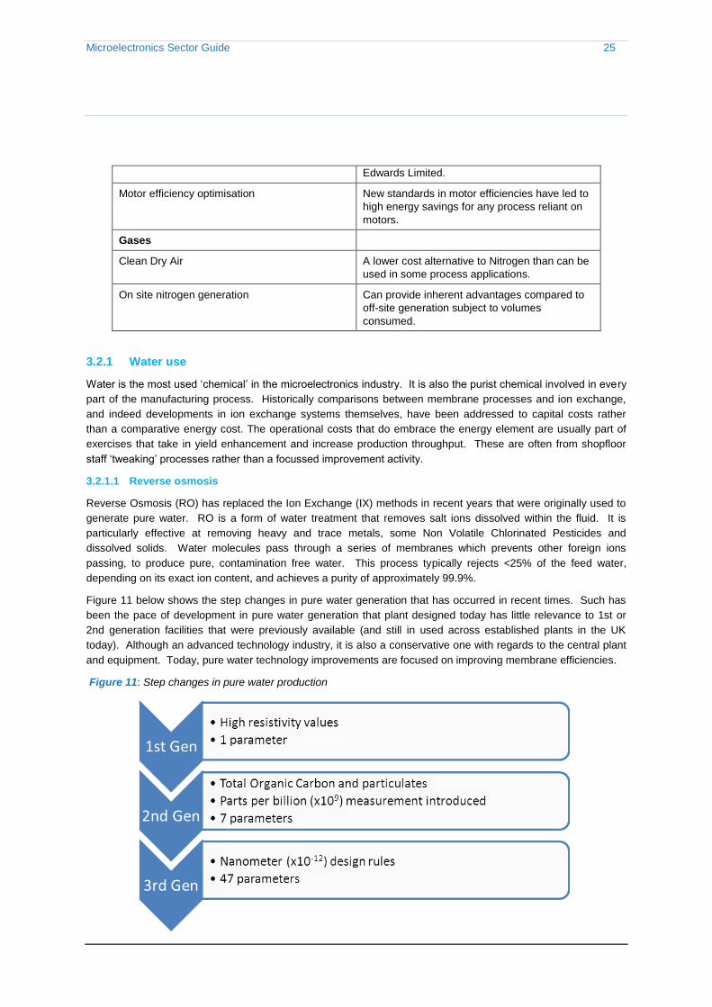
3.2.1.1 Reverse osmosis
Reverse Osmosis (RO) has replaced the Ion Exchange (IX) methods in recent years that were originally used to
generate pure water. RO is a form of water treatment that removes salt ions dissolved within the fluid. It is
particularly effective at removing heavy and trace metals, some Non Volatile Chlorinated Pesticides and
dissolved solids. Water molecules pass through a series of membranes which prevents other foreign ions
passing, to produce pure, contamination free water. This process typically rejects <25% of the feed water,
depending on its exact ion content, and achieves a purity of approximately 99.9%.
Figure 11 below shows the step changes in pure water generation that has occurred in recent times. Such has
been the pace of development in pure water generation that plant designed today has little relevance to 1st or
2nd generation facilities that were previously available (and still in used across established plants in the UK
today). Although an advanced technology industry, it is also a conservative one with regards to the central plant
and equipment. Today, pure water technology improvements are focused on improving membrane efficiencies.
Figure 11: Step changes in pure water production

Microelectronics Sector Guide 26
With the development of membranes many RO systems today, that have been retro-fitted with modern
membranes after the originals have expired, can now be operated at different parameters. For example a 2010
BW30-400HRLE (High Recovery, Low Energy) membrane is 15% more efficient than its 1990 BW30-400
counterpart although physically of the same appearance.
RO requires a higher driving pressure than the water‟s natural osmotic pressure. This pressure is exerted against
a semi-permeable membrane allowing the passage of the water molecules across the membrane and rejection of
the other molecules into a concentrate stream. To maintain this pressure the concentrate stream is “throttled” by
a valve.
Figure 12: Reverse Osmosis Membrane Energy Comparison11
Understanding exact energy savings from this technology is complex with salinity, temperature, pH, scaling
tendency, fouling index and ionic content all requiring consideration. Figure 12 shows how energy usage per unit
volume of water varies compared to feed water temperature and pressure.
Pre-heated water has process cycle time benefits that are also worth noting. Heating the water reduces its
osmotic pressure which increases the deionisation process efficiency. Whilst additional energy may be used to
pre-heat the water, significant energy savings can be made from the more efficient deionisation process. Heated
water is required for some sites as part of the process requirements such as controlling etchant rates. Pre-
heating of feed water for RO reduces the specific power from 0.78kWh/m3 at 10°C to 0.43kWh/m3 at 25°C,
realising an energy saving of 44%12
.
Lower temperatures, however, will give rise to higher quality water (i.e. number of total dissolved solids is lower).
This is due to the porous membrane contracting, relatively, compared to higher temperatures. A compromise
must be considered as smaller pores in the membranes require a higher pressure, and therefore greater energy
use, to pass the water though for the same flow rate. A rule of thumb used in RO design assumes flow rate
varies by 2.5% per 0.5°C change in feed water temperature.
Water purity has improved vastly as the RO process has been developed. Comparing today‟s purity level with
past RO or ion exchange processes is not viable due to material changes and advancing technology. RO is
11
Courtesy of Terry Cummings 12
Feedback from RO study at overseas facility
Microelectronics Sector Guide 27
generally reported to be approximately one third of the cost, compared to the ion exchange process it was
developed to replace, but it also achieves three times the water purity13
.
Recovery Reverse Osmosis (RRO) is a process enhancement that utilises the higher pressure to further treat the
water recovering a portion for re-use and absorbing the residual pressure energy for useful use. Thus, instead of
decaying pressure across a valve it is used to improve the water recovery of the overall RO system and makes
use of energy that would otherwise be wasted.
A design exercise for a UK wafer Fab (that was not progressed due to capex restrictions) provides an illustration:
Capital cost for RRO installation was £175k versus a payback possible in just over one year. The savings were
generated through recovered water, reduced electrical power and anti-scalant chemicals. This example takes
account of efficiencies and process realigning required to modify the existing system. This may not be
necessarily the case in all instances, further highlighting the potential of RRO.
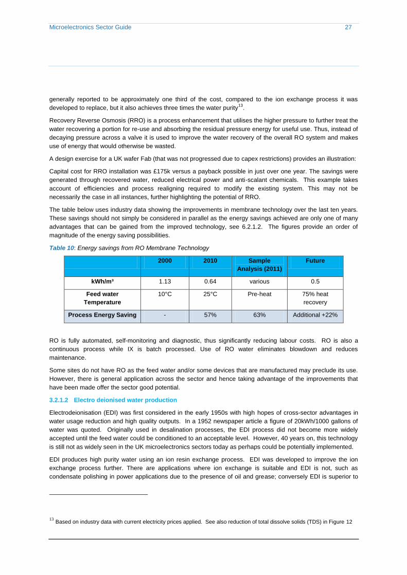
The table below uses industry data showing the improvements in membrane technology over the last ten years.
These savings should not simply be considered in parallel as the energy savings achieved are only one of many
advantages that can be gained from the improved technology, see 6.2.1.2. The figures provide an order of
magnitude of the energy saving possibilities.
Table 10: Energy savings from RO Membrane Technology
2000 2010 Sample
Analysis (2011)
Future
kWh/m³ 1.13 0.64 various 0.5
Feed water
Temperature
10°C 25°C Pre-heat 75% heat
recovery
Process Energy Saving - 57% 63% Additional +22%
RO is fully automated, self-monitoring and diagnostic, thus significantly reducing labour costs. RO is also a
continuous process while IX is batch processed. Use of RO water eliminates blowdown and reduces
maintenance.
Some sites do not have RO as the feed water and/or some devices that are manufactured may preclude its use.
However, there is general application across the sector and hence taking advantage of the improvements that
have been made offer the sector good potential.
3.2.1.2 Electro deionised water production
Electrodeionisation (EDI) was first considered in the early 1950s with high hopes of cross-sector advantages in
water usage reduction and high quality outputs. In a 1952 newspaper article a figure of 20kWh/1000 gallons of
water was quoted. Originally used in desalination processes, the EDI process did not become more widely
accepted until the feed water could be conditioned to an acceptable level. However, 40 years on, this technology
is still not as widely seen in the UK microelectronics sectors today as perhaps could be potentially implemented.
EDI produces high purity water using an ion resin exchange process. EDI was developed to improve the ion
exchange process further. There are applications where ion exchange is suitable and EDI is not, such as
condensate polishing in power applications due to the presence of oil and grease; conversely EDI is superior to
13
Based on industry data with current electricity prices applied. See also reduction of total dissolve solids (TDS) in Figure 12

Microelectronics Sector Guide 28
ion exchange such as silica and boron reduction in ultra pure water. For a meaningful comparison the inputs and
expected outputs have to be comparable for the processes being considered.
EDI is typically used after RO/RRO processing to further demineralise the water. An electrical potential drives
the ions through a set of permeable membranes, separating ions and demineralising the water further. It is
considered advantageous for the following reasons:
Low energy consumption;
No chemical requirement – further reducing the associated hazard risk;
Regeneration of resins reducing maintenance requirements; and
Low operational costs.
EDI will typically recover 95% of the feed water. A continuous EDI machine with a capacity of 15,000L/hr
requires just 4.5KW of input energy. This is also supported by the fact that EDI is continuous but ion exchange
involves batch processing.
The amount of electrical power required to continuously regenerate the stack is directly proportional to the ions to
be exchanged (removed into the concentrate stream). It can be assumed that cost savings will directly relate to
energy reduction. It also follows that the performance of an RO process has a direct effect on the performance of
EDI. For this reason it is usual to deploy a two pass RO in EDI applications.
The use of EDI is a proven technology outside of the UK. Using first principles and industry data based upon an
installation in Singapore it has been possible to provide a comparison costs per regeneration14
as shown in the
table below.
Table 11: Comparison of EDI and RO technologies
RO/IX RO/EDI RRO/EDI
2009 Case Study
(£/regeneration)
£2,023 £594 £156
Estimated saving - 71% 90%
Another case study was completed recently for a system in Johor Bahru, Malaysia. Power, water and local cost
differences compared to the UK do not allow a similar cost comparison to be made as in Table 9 but the site has
confirmed a 17-19% cost saving per unit volume of pure water between RO/EDI and the RO/IX technologies.
There is a convincing argument for EDI to be followed up in more detail in the future as there are proven energy,
cost and resource usage benefits from this technology.
These savings are likely to be through energy reduction or other process changes but the additional benefits of
EDI, aside from the energy saving potential, should also be noted:
No use or bulk storage of chemicals;
No chemical waste and no wastewater to neutralise;
No interference of clean systems with dirty chemicals;
No invasive procedures;
14
EDI parameters as based on proven data from in Singapore for 50gpm stack latest development packed concentrate chamber units commissioned 18 months ago. Regeneration quantities depend on speed of process and number of processes. One regeneration is for a set volume of water passed through all phases in the deionisation process. A mixed bed regeneration process produces approximately 34cu.m of water, EDI over 47cu.m. Costs have been converted to reflect UK rates.

Microelectronics Sector Guide 29
No remixing of resins;
No rinsing;
No expensive Nitrogen Gas to remix;
Reduced Operator skills base;
No interruption to service flow – Continuous Regeneration;
Fully Automatic and Self Monitoring;
Reduced HPM Risk; and
Reduced Footprint, Height and Foundation Loads.
3.2.1.3 Water cooling opportunities
Reducing cooling water flow requirements has been typically received in this study as now being a best practice
industry standard to aim for. This is primarily due to recently escalating utilities costs in both water and electricity.
There are process limits to be considered when changing water temperatures which are invariably influenced by
other processes in the Fab and the individual machines and processes used. A cooling water ring main can be
installed, where possible, which has the benefit of removing a substantial number of independent pumps in the
system.
Typically there are three cooling systems - glycol, CHW (chilled water) and evaporative:
Glycol systems are used where low and very precise humidity control is required. Easing the humidity set
points and / or also control differentials has proven to obviate the need for glycol systems.
CHW is used for sensible cooling of air handling systems, dehumidification in less demanding areas and
Process Cooling Water (PCW).
Evaporative cooling makes use of the climatic conditions in parts of the UK utilising adiabatic cooling towers.
All of these systems have a cooling element and a rejection of heat element. This reject heat is usually in the
order of 20~22°C. This heat can be used for process use i.e. enhancing RO performance, frost coils, space
heating and pre-heat of domestic hot water though no data has been collected related to these options.
Reducing cooling water requirements is largely optimising available central systems while retaining process tool
and manufacturing requirements. Evolution of tools to increase efficiencies and hence heat losses is being
introduced but overall reduction in cooling demand from these activities may not be significant compared with the
other opportunities.
3.2.1.4 Rinse optimisation
Ultra pure water is the most expensive utility in a Fab when combining process costs and supply costs. An option
used by some Fabs to reduce this usage is the „quick dump rinse‟ after the etching process. The usage is
controlled by resistivity value of the water and is then purged when resistivity falls out of limits. It can also take
advantage of free cooling through heat recovery from other processes.
Microelectronics Sector Guide 30
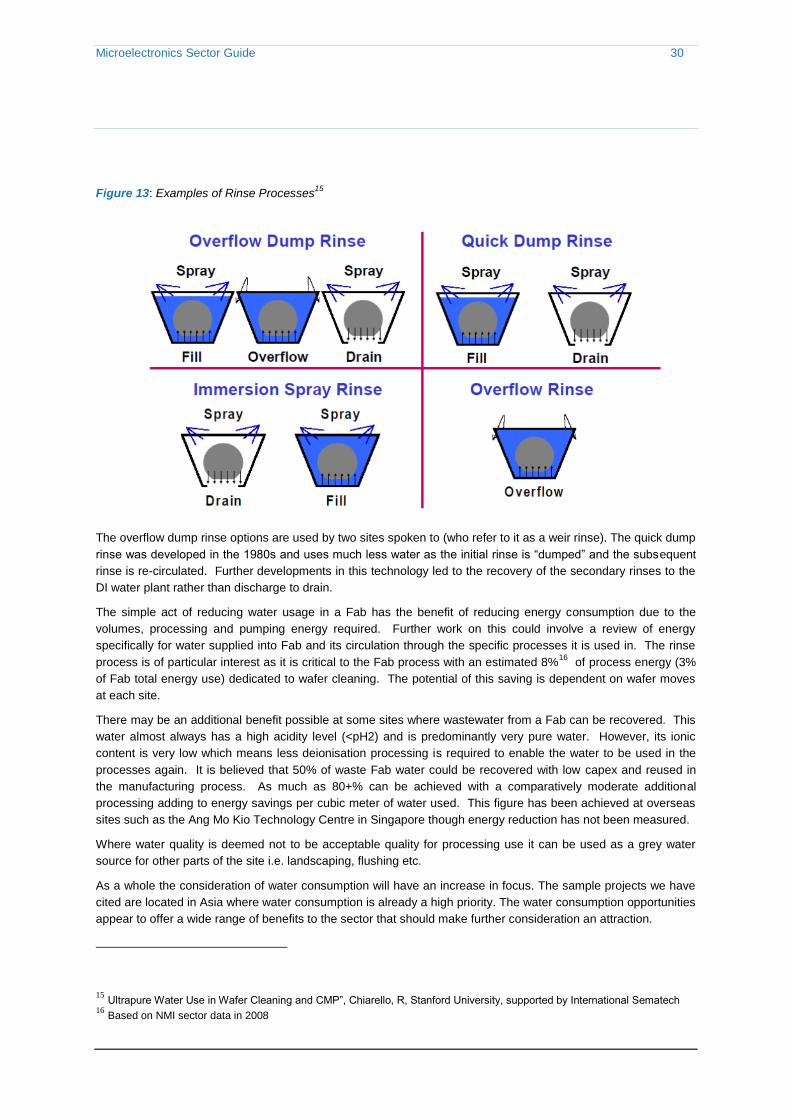
Figure 13: Examples of Rinse Processes15
The overflow dump rinse options are used by two sites spoken to (who refer to it as a weir rinse). The quick dump
rinse was developed in the 1980s and uses much less water as the initial rinse is “dumped” and the subsequent
rinse is re-circulated. Further developments in this technology led to the recovery of the secondary rinses to the
DI water plant rather than discharge to drain.
The simple act of reducing water usage in a Fab has the benefit of reducing energy consumption due to the
volumes, processing and pumping energy required. Further work on this could involve a review of energy
specifically for water supplied into Fab and its circulation through the specific processes it is used in. The rinse
process is of particular interest as it is critical to the Fab process with an estimated 8%16
of process energy (3%
of Fab total energy use) dedicated to wafer cleaning. The potential of this saving is dependent on wafer moves
at each site.
There may be an additional benefit possible at some sites where wastewater from a Fab can be recovered. This
water almost always has a high acidity level (<pH2) and is predominantly very pure water. However, its ionic
content is very low which means less deionisation processing is required to enable the water to be used in the
processes again. It is believed that 50% of waste Fab water could be recovered with low capex and reused in
the manufacturing process. As much as 80+% can be achieved with a comparatively moderate additional
processing adding to energy savings per cubic meter of water used. This figure has been achieved at overseas
sites such as the Ang Mo Kio Technology Centre in Singapore though energy reduction has not been measured.
Where water quality is deemed not to be acceptable quality for processing use it can be used as a grey water
source for other parts of the site i.e. landscaping, flushing etc.
As a whole the consideration of water consumption will have an increase in focus. The sample projects we have
cited are located in Asia where water consumption is already a high priority. The water consumption opportunities
appear to offer a wide range of benefits to the sector that should make further consideration an attraction.
15
Ultrapure Water Use in Wafer Cleaning and CMP”, Chiarello, R, Stanford University, supported by International Sematech 16
Based on NMI sector data in 2008
Microelectronics Sector Guide 31
3.2.2 Furnaces
3.2.2.1 Furnace elements
Just as a corroded or old element in a household boiler is less efficient, old or damaged elements can be
inefficient in Fab furnaces. The patented Light Gauge Overbend (LGO™) element presents a step change in
furnace efficiency and capability. Industry literature claims 40% energy saving is possible (Koyo Thermo
Systems Ltd.17
) and that LGO elements can be retrofitted in some existing horizontal furnaces. They also
present a more consistent, uniform temperature profile in the cross section of the furnace with less temperature
variability at edges of the chamber (typically +/- 1°C). This has the advantage of a consistence heating process
across the wafer(s) which may assist in reducing wafer moves in a furnace.
Tetreon have confirmed that they use LGO elements in their furnaces with MRL Industries (furnace element
supplier to 2 host sites associated with this study) supplying „Black Max‟ elements that use the LGO technology.
However, it is understood that Black Max elements are only suited to low temperature furnaces (<850°C) – too
low an operating temperature in most semiconductor processes. It may however be suitable for low pressure
chemical vapour deposition which typically requires 700-850°C. Thermo Scientific do supply a 1200°C LGO Box
Furnace which suggests the technology can be used at higher temperatures in other types of furnace. The idea
of using this technology at higher temperatures may be beneficial in future furnace developments in the
semiconductor industry, including retrofittable elements. The development of this technology specific to the
furnace temperatures used in Fabs has not been developed as yet apart from in lower temperature processes
such as Chemical Vapour Deposition.
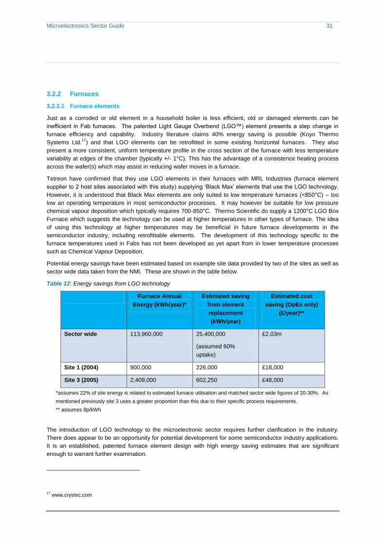
Potential energy savings have been estimated based on example site data provided by two of the sites as well as
sector wide data taken from the NMI. These are shown in the table below.
Table 12: Energy savings from LGO technology
Furnace Annual
Energy (kWh/year)*
Estimated saving
from element
replacement
(kWh/year)
Estimated cost
saving (OpEx only)
(£/year)**
Sector wide 113,960,000 25,400,000
(assumed 60%
uptake)
£2.03m
Site 1 (2004) 900,000 226,000 £18,000
Site 3 (2005) 2,409,000 602,250 £48,000
*assumes 22% of site energy is related to estimated furnace utilisation and matched sector wide figures of 20-30%. As
mentioned previously site 3 uses a greater proportion than this due to their specific process requirements.
** assumes 8p/kWh
The introduction of LGO technology to the microelectronic sector requires further clarification in the industry.
There does appear to be an opportunity for potential development for some semiconductor industry applications.
It is an established, patented furnace element design with high energy saving estimates that are significant
enough to warrant further examination.
17
www.crystec.com

Microelectronics Sector Guide 32
Figure 14: Light Gauge Overbend Elements18
3.2.2.2 Furnace insulation
In discussing with Tetreon and consulting Thermo Scientific literature it was understood that electrical
consumption of furnaces is highest during temperature ramp up. This removes the viability of the solution of
reducing furnace temperatures during standby times.
Most furnace heat losses are through air or water movements that are typically minimised in design rather than in
operation improvement. Furnace insulation materials are typically glass, ceramic or carbon fibre based. Vacuum
insulation, a potential retrofit solution for horizontal furnaces, works just as a vacuum flask does by reducing heat
radiation to a minimum. Tetreon have used carbon based vacuum insulation successfully with other customers
to those involved in this study but the solution was found to only be cost effective for furnaces operating above
1850°C. It is particularly successful for furnaces operating with a highly volatile atmosphere where the added
insulation of this type is a fundamental requirement rather than an advantageous add-on19
.
A form of vacuum insulation used by Thermo Scientific, Moldatherm®, is a high temperature fibre vacuum-formed
around the furnace chambers. According to literature from Thermo Scientific it provides efficient radiant energy
release, improved temperature uniformity across the furnace chamber and rapid heat-up and cool-down
properties. Moldatherm is used in furnaces operating at 100-1100°C.
Vacuum insulation is perhaps a solution that could be considered in principle with more research required into
cost effective solutions for semiconductor specific furnaces in the future. Current operating temperatures are
between 1200°C and 1500°C, out of the capabilities or value for the examples seen thus far.
3.2.3 Pump stand-by operation
3.2.3.1 Vacuum pumps
Pumps can be one of the largest energy users in a Fab, typically 50-60% of process energy. Microelectronic
Fabs have many numbers of pumps across the operations. Due to process control requirements it is not possible
to shut down some of these pumps even when there is temporarily zero through-put. However a structured asset
management plan to incorporate new pumps into an existing Fab would be beneficial to overall operating costs
and reduced energy usage at any semiconductor Fab.
18
Pictures from www.mrlind.com and Thermo Electron Corporation literature 19
Telephone conversation with Iain McGregor, Sales Manager, Tetreon

Microelectronics Sector Guide 33
Vacuum pump manufacturer Edwards Ltd, a leading global supplier in vacuum pumps, especially those for the
semiconductor industry, advocates a whole range of new, energy efficient pumps. Edwards have set corporate
aims to reduce energy usage of all their pumps including 10% energy reduction on heavy duty pumps‟ operations
specifically for the semiconductor industry.
There is, however, the barrier of substantial capital expenditure being required if a planned pump replacement
regime was to be undertaken in a single Fab. A phased replacement roll-out using new pumps when old ones
become uneconomical to repair would be a suitable option if long term investment planning was considered by
the sites.
3.2.3.2 Load lock vacuum pumps
A load lock allows a wafer to pass from the cleanroom into a process chamber for lithography via a compartment
having a door at each end. The outer door opens with the vacuum pump off, closes and the vacuum pump pulls
down the pressure in the chamber before the inner door opens and the wafer passes into the chamber where an
inert gas (usually nitrogen) is introduced to reduce surface oxidation. If the process chamber conditions do not
equal the vacuum chamber conditions, the doors will not open. Once the wafer is in the processing chamber
there is no process requirement to maintain the vacuum within the load lock. Understanding the throughput
impacts and energy use implications of constantly running load lock pumps compared to variable loading is
required to assess the energy usage requirements.
One such load lock pump that could be considered for this opportunity is the iXL120 by Edwards, launched in
2010, which advocates a „Green Mode‟. This product allows reduced energy usage during idle periods. This
pump is rated to consume circa. 83% less power for the same pumping capacity (see Figure 15 below).
Figure 15: Load lock pump efficiency improvements20
Active Utility Control (AUC) is a new technology to improve vacuum pump efficiency through optimising pump
speed, water consumption and nitrogen consumption. This has obvious complimentary benefits in energy
savings in Fab utilities. This technology is not retrofittable to existing pumps. It is also typical that uptake will be
relatively slow until the technology is proven within the sector.
20
Courtesy of Edwards Ltd.

Microelectronics Sector Guide 34
It is understood that plans are in place where this „Green Mode‟ facility will be a standard capability on all dry
pumps, not simply a customer option. As with other vacuum pumps in Fabs there will be an aversion to high
capital spending until savings can be quantified and prove to match management payback expectations.
A basic payback estimate based on current data is given in the table below.
Table 13: Vacuum pump pay back periods
Refurbished
iQDP80 Pump
New iXL120
Green Mode
Pump
Cost (80cum/hr pump)* £6,000 £11,000
Energy Use per Pump**
(kWh/pump/year)
15,943 3,373 (78%)
Energy cost
(£/pump/year)***
£1,275 £270
Estimated payback
period
- 5 years
* Generic List price quote from Edwards Ltd. March 2011. Due to the quantity of pumps used by the
microelectronics sector it is highly likely that bulk order economies of scale will reduce these quoted list
prices.
** SEMI S23 standard is the industry standard that describes the electric power requirements and energy
conservation for a piece of equipment. It states the assumption of standard process time is 6132hr/year in
normal operation with no AUC capability included, equivalent to 70% utilisation.
*** Assumes 8p/kWh
3.2.3.3 Motor efficiencies
In conjunction with the above it is also noted, from Figure 12, that pump motors have also advanced to high
efficiency type and have become industry standard. In conjunction with the AUC control the ability for the
electrical consumption to be reduced is potentially very significant.
The payback period exceeds the industry norm and a step change, via universal sector switchover is unlikely to
occur. However, encouragement toward new pump replacement as opposed to the cheaper refurbished pump
option could see the industry achieve significant progress in the long term.
3.2.4 Compressed gases
Compressed gases have been previously classed as a facilities energy use (see Figure 7). As the generation
and use of these gases are fundamental to process parameters in a Fab this study has chosen to include
associated energy saving opportunities within the process energy use instead.
3.2.4.1 Clean dry air
In the microelectronics sector Clean Dry Air (CDA) is compressed, oil free, de-watered and filtered air.
Essentially, compressed air is a reactive gas containing all the gaseous components except a degree of water
vapour present in the atmospheric intake to the system. As such, at lower grades, it must not come into contact
with a wafer during any of the process steps when the wafer is vulnerable to contamination from oxidation. This
contamination is not necessarily particulate but can be a gas bubble or “smear” or similar. At its higher
specification levels i.e. –56°C pressure dewpoint and below, CDA can be compared to utility grade Nitrogen in
cleanliness. It is usual to provide an automatic backup between CDA to the Nitrogen. This ensures the Nitrogen

Microelectronics Sector Guide 35
system remains pressurised preventing outside contamination ingress or back-diffusion should the Nitrogen feed
be lost.
CDA maybe be used by semiconductor manufacturers as a means to remove debris from wafer surfaces.
Contamination of even microscopic particulates can cause shorts in the manufactured circuit. Similarly moisture
causes oxidation of the product also causing failure of the final component.
CDA is produced using a single compression process whereas nitrogen is produced through an air separation
process that requires two phases of compression. It is this difference that results in lower energy requirements
for CDA production.
Technologies have emerged in recent years that have improved the energy efficiency of equipment used to
generation CDA. These include:
Membrane materials improving efficiency of production for similar purity; and
Compressor off-loading – typically two vessels will be used in CDA batch production where only one is in use
at any one time in the cycle. It is possible to off-load the compressor during the other vessel‟s idling time
between cycles.
On-site generators can be sized on base output load (therefore always operating at100%) and peaks can be
controlled through liquid air back up. The liquid air can be supplied/stored separately for peak usage.
Some Fabs will not be able to utilise this technology from a product specification perspective. Its application is
also not a whole replacement to Nitrogen and in this regard it would be supplemental and process specific. The
use of CDA has already been implemented at some of the sites visited and we understand its value is universally
recognised in the sector.
3.2.4.2 On-site N2 production
Generally liquid nitrogen (LN2) is only used for cryogenic use. However LN2 is stored on site as a more efficient
means of providing Nitrogen gas (N2) for atmospheric control in Fabs. To this end, a large quantity of N2, in a
variety of phases, is required in the microelectronics industry and can sometimes provide a sound business
argument for onsite generation instead of direct deliveries.
There are two typical methods for producing N2. Cryogenic production brings in air and cools it prior to stripping
out the N2 from its other components. Although cooling is applied the air and its constituents remain in the
gaseous form. This production process achieves 99.999% purity. The adsorption process uses two vessels in a
batch process where air is passed through a membrane to separate it. This typically delivers 95-99.9% pure
nitrogen. In terms of energy use per unit of nitrogen produced both processes are similar. Cryogenic production
uses approximately 0.25-3kWh/nm3 compared to adsorption which uses 0.3-0.4kWh/nm3. These figures are
wholly dependent on the size of the plant and the pressures required.
A study was done in the 1990s on the production of liquid Hydrogen and the breakeven point between on-site
generation and direct delivery was estimated at 600,000cu.m. A Fab considered at a similar time estimated the
breakeven point for Nitrogen usage as 645,000cu.m/month (split 60/40 High Purity / Normal use derived from
LN2).
For on-site generation of gaseous nitrogen no energy is required for associated liquefaction. The energy demand
for liquefaction more than doubles the energy footprint of bulk liquid compared to on-site-produced gaseous
nitrogen (which is typically the requirement in the microelectronics sector). In terms of energy usage there is an
obvious argument that the responsibility, previously not held by the Fab, will lead to increased energy usage at a
Fab site if the supply chain option for Nitrogen is changed to on-site production. Although the energy utilisation
increases for the Fab there may be wider benefits in terms of overall energy usage in transport and the wider
supply chain.

Microelectronics Sector Guide 36
The success of this opportunity lies within the individual sites‟ N2 volume requirements and attitude to supply
security. There is also technology emerging to improve production efficiencies. Also, there may be some scope
to consider purity requirements as it is thought that energy use is directly linked purity specification.
The data gathered in this study provides some estimates of energy saving potential between these technologies
but further clarification would be needed on to develop the business case for each site.
Table 14: Compressed gas energy comparison
Offsite N2 generation Onsite nitrogen
(kWh/m³)
Onsite CDA (kWh/m³)
Site 1 - - 0.1
Site 3 - 0.42 0.22
BOC averages 0.44 0.25-0.3 0.3-0.4
3.3 Process summary
The study and stakeholder engagement has given rise to greater understanding of current drivers in the
microelectronics sector and potential additional studies related to energy reduction. It is clear that throughput
and payback are key considerations for any process changes and the business case for most solutions will have
to be reviewed on a site by site basis.
Table 15 below provides a summary of the opportunities discussed with an estimate of the potential application to
energy savings in the Process areas.
Table 15: Process opportunities summary
Business Case
Opportunity
% Saving by
process
% of Site
Energy Use
Uptake
Within
10years
Estimated Process
Saving Quantification
Estimated
Annual
Sector Saving
(tCO2/year)
Innovation
RO Membrane
placement 63% min. 1.9% 30% 0.598MWh/site/year 2,544-4,464
RO/IX RO/EDI or
RO/EDI RRO/EDI ~70% 2% 20% £30-40/m
3 water 728-2,975
Good Practice
Rinse
Optimisation 8% 3% 50% 1,500MWh/site/year 10,486
Furnace Elements 40% 2% 60% 1,628MWh/site/year 13,841
On-site N2
generation ~30% 1.2% 50% 1,060MWh/site/year 7,500
On-site CDA
generation 30-40% 1.2-1.9% 50% 1,060-1,660MWh/site/year 7,500-11,760
Load Lock Green
Mode pumps 75-85% up to 7% 30% 2,500MWh/site/year 11,810

Microelectronics Sector Guide 37
The following work elements will need to be factored into a business case to provide further verification as to the
order of magnitude for any potential saving and to confirm implementation feasibility. Therefore the work scopes
are considered more appropriate to business case development:
Establish energy savings from the introduction of RO technology based on unit site considerations and
comparing this to the batch ion exchange process;
Cost benefit analysis for EDI technology in the sector to develop a robust business case for other sites to
learn from;
Comparison study of rinse options for current UK sites and understanding of quantified energy use for each
option;
Encourage cross-sector learning particularly in the evaluation of technologies in furnace elements and
insulation for use in the microelectronics industry;
Cost benefit analysis in planned asset management of pumps to replace with more efficient models; and
Establish the energy saving potential for reduced idling for load lock pumps and payback for implementation.

Microelectronics Sector Guide 38
4 Facilities
The following section reviews energy consumption across site utilities within the Fab facility. These which are
needed to maintain the specific environment required for high quality semiconductor manufacturing.
4.1 Facilities areas
4.1.1 Clean room
The conditions under which the processes, as described in Section 2.8.1 can work to successfully transform the
silicon into semiconductor devices require an environment that is essentially contaminant free.
The process chambers in which the processes are carried out typically operate under vacuum where elemental,
molecular and particulate contaminants are rigorously controlled. This requirement for cleanliness extends to the
general manufacturing environment where the wafers are exposed.
As a result of the cleanliness requirements, semiconductor device fabrication is carried out in cleanrooms. To
maintain the required level of cleanliness the air entering a cleanroom from outside is filtered to exclude dust and
the air inside is constantly re-circulated through high efficiency particulate air (HEPA) and/or ultra low particulate
air (ULPA) filters to remove internally generated contaminants.
ISO14644 is an international standard that defines cleanroom design, construction and testing for the specified
levels of cleanliness required. This standard covers all types of clean environment such as microelectronic
production as well as aseptic suites and medical device facilities.
Staff enter and leave through airlocks (sometimes including an air shower stage), and wear protective clothing
including hats, face masks, gloves, boots and coveralls.
Equipment inside the cleanroom is designed to generate minimal air contamination. Cleanroom furniture is also
designed to produce a minimum of particles and to be easy to clean.
Cleanrooms are typically maintained at a positive pressure so that leakage from the space is clean air outwards
rather than dirty, unfiltered air coming in.
Cleanrooms have many plant items which maintain the clean, controlled environment. These include:
Ventilation plant – e.g. central air handling units, fan filter units, fan towers
Extract plant – e.g. process extract fans, fume cupboards
Heating plant – e.g. boilers
Cooling plant – e.g. air cooled chillers, cooling towers & water cooled chillers

Microelectronics Sector Guide 39
Humidification plant – e.g. steam boilers, electrode boilers, mist humidifiers
A typical cleanroom arrangement has been indicated in the following diagram.
Figure 16: Typical Cleanroom Facilities Requirements: the area between the AHU and the work zone (+)ve
pressure; the area between the work zone and the service zone (-)ve pressure
As discussed in Section 2.9 the primary facility energy consumers are ventilation, cooling and humidification.
Areas for investigation for significant energy savings within these elements are discussed in the following
sections.
4.1.1.1 Ventilation
Ventilation is provided within the facility to filter contaminants, ensure pressure regimes between clean and dirty
areas, to dissipate heat gain in the space and provide a comfortable environment in which to work.
Table 16, an excerpt from ISO14644-4, highlights the different levels of cleanliness and their associated
recommended velocities and air change rates.
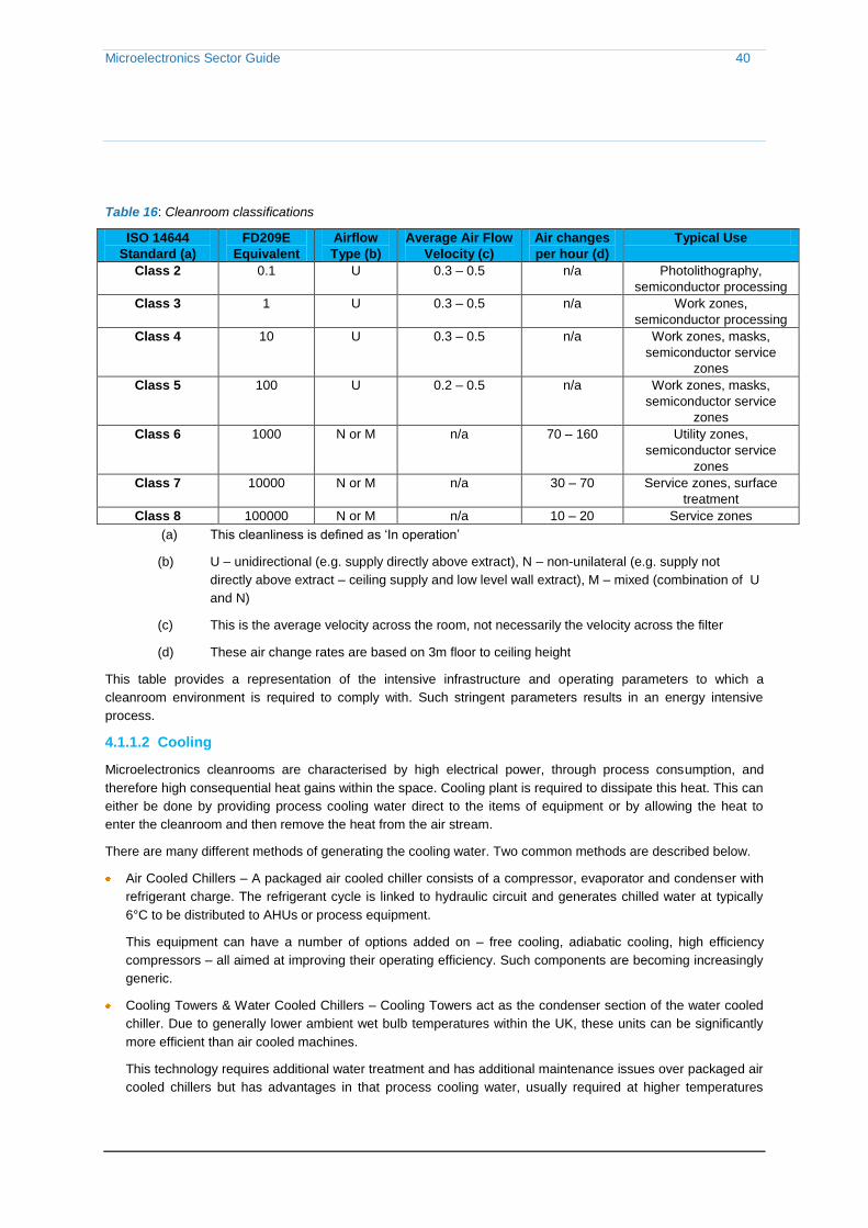
Microelectronics Sector Guide 40
Table 16: Cleanroom classifications
ISO 14644
Standard (a)
FD209E
Equivalent
Airflow
Type (b)
Average Air Flow
Velocity (c)
Air changes
per hour (d)
Typical Use
Class 2 0.1 U 0.3 – 0.5 n/a Photolithography,
semiconductor processing
Class 3 1 U 0.3 – 0.5 n/a Work zones,
semiconductor processing
Class 4 10 U 0.3 – 0.5 n/a Work zones, masks,
semiconductor service
zones
Class 5 100 U 0.2 – 0.5 n/a Work zones, masks,
semiconductor service
zones
Class 6 1000 N or M n/a 70 – 160 Utility zones,
semiconductor service
zones
Class 7 10000 N or M n/a 30 – 70 Service zones, surface
treatment
Class 8 100000 N or M n/a 10 – 20 Service zones
(a) This cleanliness is defined as „In operation‟
(b) U – unidirectional (e.g. supply directly above extract), N – non-unilateral (e.g. supply not
directly above extract – ceiling supply and low level wall extract), M – mixed (combination of U
and N)
(c) This is the average velocity across the room, not necessarily the velocity across the filter
(d) These air change rates are based on 3m floor to ceiling height
This table provides a representation of the intensive infrastructure and operating parameters to which a
cleanroom environment is required to comply with. Such stringent parameters results in an energy intensive
process.
4.1.1.2 Cooling
Microelectronics cleanrooms are characterised by high electrical power, through process consumption, and
therefore high consequential heat gains within the space. Cooling plant is required to dissipate this heat. This can
either be done by providing process cooling water direct to the items of equipment or by allowing the heat to
enter the cleanroom and then remove the heat from the air stream.
There are many different methods of generating the cooling water. Two common methods are described below.
Air Cooled Chillers – A packaged air cooled chiller consists of a compressor, evaporator and condenser with
refrigerant charge. The refrigerant cycle is linked to hydraulic circuit and generates chilled water at typically
6°C to be distributed to AHUs or process equipment.
This equipment can have a number of options added on – free cooling, adiabatic cooling, high efficiency
compressors – all aimed at improving their operating efficiency. Such components are becoming increasingly
generic.
Cooling Towers & Water Cooled Chillers – Cooling Towers act as the condenser section of the water cooled
chiller. Due to generally lower ambient wet bulb temperatures within the UK, these units can be significantly
more efficient than air cooled machines.
This technology requires additional water treatment and has additional maintenance issues over packaged air
cooled chillers but has advantages in that process cooling water, usually required at higher temperatures

Microelectronics Sector Guide 41
(~15°C) can be generated very efficiently. Independent of the type of cooling plant, the control is critical to the
efficiency of the cooling system.
4.1.1.3 Humidification
Accurately controlled humidity levels are required within the cleanrooms to maintain quality control within the
process (e.g. photoresist layer thickness can alter with humidity fluctuations).
Humidity control is traditionally achieved by injecting steam direct into the air stream. The steam can be
generated via central gas boilers or by gas fired steam generators or more typically via electrode steam boilers.
These electrode boilers are preferred as they offer very high levels of control however they are a high consumer
of electrical energy.
Alternatives to electrode steam boilers are adiabatic humidification such as high pressure misting systems and
ultrasonic systems.
A typical comparison of the three technologies suggests that adiabatic or mist humidification is a significantly
lower energy intensive method of providing humidity control.
Table 17: Humidification examples
System Power Required
kW/kg/h
Comments
Electrode steam boiler 0.75 Needs softened water
Ultrasonic 0.14 Needs RO water
High pressure misting 0.01 Needs RO water
4.2 Facilities energy use
Figure 17: Typical Facilities Energy Inputs

Microelectronics Sector Guide 42
Figure 17 indicates the utility provision to the various cleanroom plant and equipment.
The figure enforces the requirement for electrical and gas input into the process. The typical split on sites can
vary from 90/ 10% (electrical/ gas) to 60/30%. The amount of gas used depends greatly on location (external
climate conditions) and process (semiconductor manufacture uses more electricity than wafer fabrication).
The breakdown of the energy consumption associated with the primary elements is presented in the following
table:
Table 18: Plant and Equipment power consumption
Plant/Equipment % Power Consumption tCO2/annum
Air Handling Plant 13 - 31 100 – 230,000
Cooling Plant 20 - 26 150 – 200,000
Process Extract 3 – 8 25 – 60,000
4.2.1 Potential energy saving opportunities
Following our review of the system configurations observed at the site we have identified opportunities that we
believe may offer wholesale savings and that could be replicated across similar sites (acknowledging that some
fundamental adjustment to existing infrastructure maybe required.) These opportunities are outlined in the
following sections.
4.2.1.1 Reduced air change rates
The design guidance for the ventilation of cleanrooms appears to be based on historical assumption and practice.
During our investigation we have not been able to derive the robust science behind the guideline.
ISO 14644 recommends air change rates of 240-600 times the room volume per hour within Class 2 to 5
cleanrooms to achieve the required levels of cleanliness.
This represents very high energy consumption for the facility at the central air handling plant or through fan filters
or fan towers.
International research by Sematech has shown that cleanliness is not necessarily affected by the number of air
changes and that air change rates can potentially be reduced without suffering any detriment to the level of
cleanliness. The research indicates that significant energy savings could be realised if the parameters were
relaxed.
Other similar research exists by several different companies and associations and seemingly a requirement to
change the current guidelines is gaining momentum.
One study documented that 10 different Class 5 cleanrooms were operating between 94 and 276 air changes as
opposed to the 240-600 recommended within ISO 14644. This represents a reduction in velocity through the
components and filters of 6 times (600acph to 97acph) which translates to significant energy savings.
In order to ensure that the air cleanliness is not compromised by reducing air change rates, continuous particle
monitoring can be implemented within the cleanrooms to provide feedback and raise alarms if conditions are not
being met.
Some of the sites that were visited had considered and/or experimented with reducing their air change rates but
without a confirmed change in legislation the progression appears to be cautiously empirical. Additionally,
new/refurbished facilities may suffer from guidelines that are overly prescriptive.

Microelectronics Sector Guide 43
To provide an indication of the potential savings we have assumed a unit sample cleanroom space and assigned
the maximum and minimum guideline ratings to assess the difference in associated energy consumption.
Table 19: Air Change energy saving (based on100m2, Class 5 area)
Cleanroom
Parameters Min Max
Fresh Air AHU 0.2 0.5 m/s
Fan Filter Units 240 600 Ac/hr
Sensible Cooling
Coils
20 50 M3/s
Process Exhaust 91 202 MWh/annum
Saving 55% -
We have repeated the analysis to assess the difference in the guidelines prescriptions for the two common forms
of cleanroom ventilation: Fan Filter assemblies and Central AHU.
Table 20: AHU and Fan Filter savings
100m
2 Class 100 Cleanroom
Scenario 1
Central AHU
Scenario 2
Fresh Air AHU; Fan Filter Units; Sensible
Cooling Coils
Guidelines Min Mid Max Min Mid Max
m/s 0.2 0.3 0.5 0.2 0.3 0.5
tCO2 49 83 286 50 56 110
Saving 83% 72% - 55% 49% -
The above table should take the following into account:
Process extract balance also impacts upon required make-up air provision;
A minimum clean down ratio has to be maintained;
The ability to reduce air change rates in highly variable across the industry; and
Airflow requirements are prescriptive to the configuration of the cleanroom. Therefore, a general rule cannot
necessarily be applied across the sector.
Microelectronics Sector Guide 44
4.2.1.2 Filter Coverage
Industry experience has established that, in a 3.5m clear height manufacturing clean room, 2.25m/s is the
minimum velocity required to maintain particle counts at the work level, parallel airflow over equipment around
the Fab and to generally mitigate buoyancy of air above the working space due to convection effects from the
equipment. A 0.5m/s velocity has only been necessary, and then only localised, in high bay cleanrooms used in
12” wafer fabrication.
The improvement in filter efficiency has been a key driver in the reduction of air change rates and the extent of
filter coverage can greatly affect the subsequent supply air volume.
It is this sort of practice that allows energy consumption to be reduced whilst maintaining high levels of air
cleanliness. Other factors such as fan efficiency, ability of out-of-hours setback in the ventilation plant, options to
vary flow according to particle counts also play a major part in effective Fab energy reduction.
Best practices related in this area are:
Table 21: Best practices in filter usage
Low Face Velocity Mini Environments
Demand Control Filtration Fan Efficiency
Correct Plant Sizing Filter Type
Recirculatory Ventilation FFU Efficiency
4.2.1.3 Air side free cooling
Air side free cooling is an adopted approach employed in other industry sectors, typically that of the commercial
construction sector. Free cooling is typically achieved by supplying fresh air directly to the facility. The more
stringent environmental requirements of the cleanrooms mean that direct cooling using fresh air could be
problematic as humidity and contamination control would be more difficult to achieve.
However, a potential approach is to use airside economisers to provide indirect free cooling. The feasibility of
implementing this option will need to look at space constraints and issues associated with installation at an
existing facility though in principle has retrofit potential in UK Fabs.
Where current sensible cooling coils are utilised we believe that potential for this option exists. The following
diagram shows the distribution of ambient air conditions for London as a representative example of UK weather.
It can be seen that for a significant portion of the year free cooling, is available.
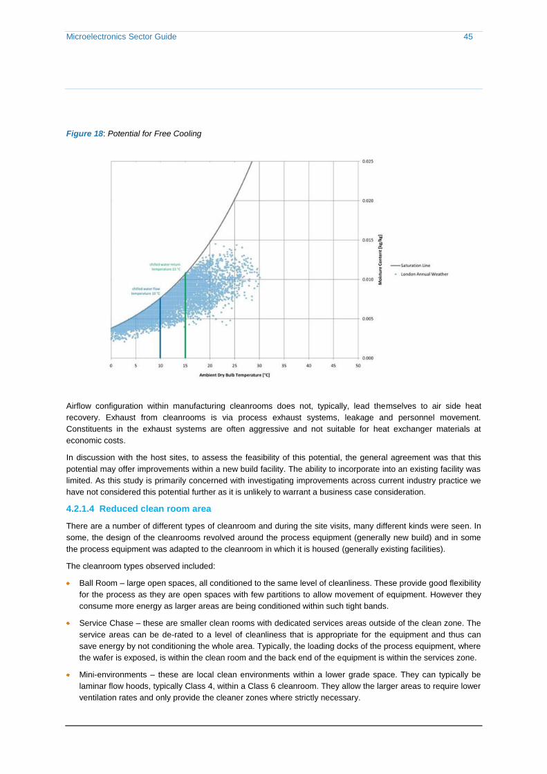
Microelectronics Sector Guide 45
Figure 18: Potential for Free Cooling
Airflow configuration within manufacturing cleanrooms does not, typically, lead themselves to air side heat
recovery. Exhaust from cleanrooms is via process exhaust systems, leakage and personnel movement.
Constituents in the exhaust systems are often aggressive and not suitable for heat exchanger materials at
economic costs.
In discussion with the host sites, to assess the feasibility of this potential, the general agreement was that this
potential may offer improvements within a new build facility. The ability to incorporate into an existing facility was
limited. As this study is primarily concerned with investigating improvements across current industry practice we
have not considered this potential further as it is unlikely to warrant a business case consideration.
4.2.1.4 Reduced clean room area
There are a number of different types of cleanroom and during the site visits, many different kinds were seen. In
some, the design of the cleanrooms revolved around the process equipment (generally new build) and in some
the process equipment was adapted to the cleanroom in which it is housed (generally existing facilities).
The cleanroom types observed included:
Ball Room – large open spaces, all conditioned to the same level of cleanliness. These provide good flexibility
for the process as they are open spaces with few partitions to allow movement of equipment. However they
consume more energy as larger areas are being conditioned within such tight bands.
Service Chase – these are smaller clean rooms with dedicated services areas outside of the clean zone. The
service areas can be de-rated to a level of cleanliness that is appropriate for the equipment and thus can
save energy by not conditioning the whole area. Typically, the loading docks of the process equipment, where
the wafer is exposed, is within the clean room and the back end of the equipment is within the services zone.
Mini-environments – these are local clean environments within a lower grade space. They can typically be
laminar flow hoods, typically Class 4, within a Class 6 cleanroom. They allow the larger areas to require lower
ventilation rates and only provide the cleaner zones where strictly necessary.
Microelectronics Sector Guide 46
Dependent upon the layout of the cleanrooms and the nature of the process, the cleanrooms could potentially be
modified to reduce the amount of area that needs to be conditioned to full cleanroom levels.
4.2.1.5 Chilled water system optimisation
Advances in chiller technology of the last five years have allowed novel approaches to chiller and chilled water
system control to be implemented. Some of these opportunities are outlined below:
Condenser Water Temperature Control/ Reset – Where water cooled chilled water systems are used it is
typical to control the cooling towers to maintain a temperature set point for the water supplied to the chillers.
A number of alternative control strategies are available that can result in significant energy savings. These
look at the combined control of cooling towers and chillers to optimise the total energy consumption. There is
evidence that indicates such operating strategies can yield savings in excess of 20% over conventionally
controlled systems. For a recent project21
it was found that reducing condenser water temperature from 29°C
to 20°C resulted in 80% improvement in coefficient of performance (COP) from 6 to 10. Proprietary strategies,
such as the Hartman Loop, are available but tend to be expensive to implement.
Free Cooling Chillers – Free cooling chillers, which employ additional heat exchangers to directly cool the
chilled water under low ambient temperature conditions, are now increasingly common particularly in
applications where a year round cooling load exists. They show most benefit in situations where higher chilled
water temperatures can be tolerated. Assessment of energy saving should be carried out on a case by case
basis based on actual operating conditions. On recent data centre type projects, which have high air change
rates and high year round cooling requirements, significant savings have been achieved22
. Free cooling can
also be implemented on water cooled chillers and cooling towers by incorporating additional heat exchangers.
Use of closed circuit towers in series with air cooled chillers can also give free cooling benefits.
Chilled Water Temperatures – On some of the sites visited all chilled water is generated at a single
temperature and where a higher temperature is required (e.g. sensible cooling coils) mixing circuits are
employed. Overcooling of chilled water results in a significant use of energy. Consideration should be given
to providing separate systems to serve those areas which require temperatures that are significantly lower
than the temperature generally required. On one of the sites visited a chilled water temperature of 4°C is
required to fresh air handling plant to a specific area. By serving this area using dedicated plant it would be
possible to elevate the general chilled water flow temperature.
We are aware that a 2008 NMI report has already published guidelines associated with chilled water
temperatures and optimisation. The report contents and our previous comments generally correlate with each
other. The NMI report is readily available to the industry and, whilst our observations indicated that not all
guidelines may be implemented industry wide, the availability of this data negates the need for this report to
consider this energy saving potential further.
21 Observation made through previous Arup project 22
Data for free cool versus non-free cool readily available from Chiller manufacturers

Microelectronics Sector Guide 47
4.2.1.6 Cleanroom utilities and humidification
The following provides a pictorial of the humidification process undertaken in the air handling plant;
Figure 19: Psychrometric Chart
As discussed in Section 4.1.1. 3 the humidification process can be undertaken by different elements that will vary
the energy consumption at the site.
By repeating the analysis of a sample cleanroom area we can highlight the potential differences in consumption
between the differing humidification elements as follows:
Table 22: Humidification elements (Excludes Maintenance; Water Quality; Blow down requirements)
Humidification Element Power Rating Annual CO2 Savings
Electrode Mist Electrode Mist
38 0.3 27 9.2
(Cleanroom parameters: Area - 100m2;Class 5; Fresh Air AHU; Fan Filter Units; Sensible
Cooling Coils; Process Exhaust.)
Table 22 above indicates a potential saving of >35% for the mist humidifier over an electrode type (estimate due
to impact of water treatment, heating of air stream, fan power and water recirculation). There is no specific data
available as to how much energy is consumed through humidification. The consumption figures across the
industry are likely to vary greatly.

Microelectronics Sector Guide 48
The sample cleanroom analysis indicates that humidification uses between 10 – 60% of the ventilation energy,
using London weather data, and assuming a supply air temperature of 21°C and 42%RH.
In our discussions with the host sites we understand that some installations of the mist system have been
undertaken in large refurbishment projects. This is seen as a feasible option when significant upgrades are
occurring. However, spatial constraints may restrict an industry wide undertaking of this system and its actual
operational benefits are yet to be measured.
Water quality for humidifiers in the microelectronics application can be rather more critical than a conventional
HVAC application. An example of this is Boron that is present in water. Boron is also the “N gate” dopant used in
the manufacture of the wafer device and as such is strictly controlled in all facilities. DI water would be used for
humidification purposes but this is aggressive and increasingly so when heated therefore construction cost of
humidifiers can escalate. RO water is the usually chosen device and its generation etc. is considered in section
3.2 of this report.
Mist humidification uses more water than steam humidification. Precise control of the mist system can also be
difficult resulting in potentially erratic humidification conditions.
Lastly, the cleanroom condition can sometimes be less concerned with the actual % of relative humidity that it
can with the range of humidity i.e. +/- <0.5%. Close control of the humidity is difficult to achieve with the mist
system and therefore its potential may not be wholly applicable an entire facility. Taking note of these issues a
mist system could offer significant potential savings across the industry.
4.4 Facilities summary
We have disseminated the data received from the host sites and summarised what measures have already been
implemented and highlighted the savings achieved from these measures. This list provides a summary of what
measures have been implemented previously and provides an indication of generic improvements that have
potential across the industry.
We have included an estimate of the potential % reduction of annual energy use that could be applicable for
specific building elements. Each of these figures is based on results taken from host site information and does
not necessarily represent the average % reduction across all of the sites. The % reduction figure is based on the
following equation:
A = Annual kW.hr energy reduction from enacting energy saving measure.
T = Total kW.hr energy used in the most recent year (after the energy saving measure has been enacted),
either gas or electricity.
% reduction = [A/ (T+A)]*100 (NB: Percentage saving based upon elemental consumption not site consumption)
The following table summarises the best practice measures taken across the sites visited during this study.

Microelectronics Sector Guide 49
Table 23: Facilities best practice
Energy saving measure Site 4 Site 2 Site 1 Site 3 % annual
energy
reduction
Replicable
across other
sites
General Good Practice
Power Perfection 6 X
Variable speed drives on AHUs 0.04
Chilled water control Refer to NMI CT Report 2008 for
chilled water system optimisation
10%
Chilled water use optimisation
Modern High Efficiency Chillers
Variable speed drives on
compressors
2
Variable speed drives on fan
towers
0.4
Free Cooling 0.4
Replaced light fittings with high
frequency lighting
3
Reduction of transformer losses by
dual to single transformer
operation
0.7
Application of modern insulation to
building design
8
Heat recovery and air recirculation
on AHU's
30
Variable speed air compressors 15
Pre-heating of city water using
recovered heat from chiller
condenser water
40
Heated air recovered from
compressor room extraction and
used to heat plant rooms
3
Table 24 below provides a summary of the primary ventilation opportunities discussed with an estimate of the
potential application to energy savings in the Process areas23
:
Table 24: Facilities best practice opportunities summary
Assumed
% saving
% of Site
Energy Use
Uptake
within
10years
Annual Sector
Saving
Reduced
cleanroom airflows
24% 18% 80% 40,000tCO2
Mist
Humidification
40% 18% 80% 35,000tCo2
23
Assumptions by Arup

Microelectronics Sector Guide 50
The above data is provided as a potential order of magnitude only for the sector as a whole. Some sites in the
sector have implemented, in part, reduced airflows and mist humidification resulting in savings already being
achieved. Therefore, the potential for savings in the Cleanroom environment are already documented and
generally understood across the sector if not wholly implemented.

Microelectronics Sector Guide 51
5 Opportunities
During this study, it was found that energy management is recognised as a fundamental issue within the
microelectronics sector though not necessarily a key driver for investment and change. A significant amount of
work has already been carried out by individual companies, trade associations and international research bodies.
Our work with the sector indicates a 60:40 split between utilities and process energy use although the gap is
narrowing. Energy reduction in the utilities area of the sector has been embraced by Fabs in recent years.
Improvements in the process energy use have been slower due to the inherent effect on process throughput and
quality. These processes are bespoke, precise, interlinked and highly complex.
In discussion with the host sites we have observed that activity in this area is ongoing but it would appear that a
fundamental undertaking is going to be required to make the “step change” with process elements.
The primary drivers for implementing any initiatives are legislation and financial profitability. There is an earnest
attitude toward energy savings and carbon emission reductions but, ultimately, the product and its throughput are
at the core of the fabrication facility.
5.1 Overview of opportunities
The industry can still benefit from shared experience. We believe that there is real opportunity in raising the
profile of the best opportunities that are already being implemented and that could lead to a greater integration
across the industry.
As a common example, some sites were observed to have installed high efficiency chillers but not amended
chilled water temperatures. In contrast others have amended temperatures but still run the chillers under a
manual control. Similarly energy saving opportunities found in processes were unknown to some but considered
best practice by others.
A key objective from the work was to understand the potential for energy savings that could be applied across the
sector. Therefore, the opportunities identified have primarily considered wafer moves and equipment
requirements. The observations from the site visits and data received have identified energy saving opportunities.
It has been possible to estimate potential savings though these figures have been evaluated from specific site
examples or unit representative examples. Several of the opportunities proposed identify additional benefits
outside of the scope of the IEEA such as a reduction in chemical use, improved health and safety of operatives
and reduced water consumption.
The following sections summarise the energy efficiency opportunities identified. It sets out opportunities that
could be considered as good practice and those which could fall under the category of innovation.
The following list represents a summary of general good practice opportunities presented in this report:
Reduced Air Change Rates (utilities);

Microelectronics Sector Guide 52
Chilled Water System Optimisation (utilities);
Process Free Water Cooling (process);
Set points for furnace equipment (process;
Heat reclaim: from process water and some air systems (process);
Humidification (utilities);
Switching off Ancillary Processes (utilities/process); and
High efficiency motors (process).
5.2 Process best practice opportunities
In relation to process specific opportunities the following best practice opportunities could be considered.
Table 25: Best Practice Process Opportunities
Opportunity Service Payback
(years)
% of sites
where
applicable
Estimated
Uptake
Estimated
CO2
saving by
sector
(tonnes)
Comments
Furnace
vacuum
insulation
Furnace - 100% 10% - Further research and
development needed
including more in depth
semiconductor industry
benefit analysis but
insulation of furnaces
key to process efficiency
Stand-by
options for
load lock
vacuum
pumps
Process 5 80+% 30% 9,500 The technology is
already available but
higher capital investment
requirements have led to
a slow uptake. To gain
whole scale
implementation further
research is needed to
understand quantified
energy savings and
ensure product quality is
not compromised.
Asset
management
and
replacement
plan for
other
vacuum
Process 5 per
pump
100% 30% 11,800 Immediate set up
possible but by nature of
solution will be a long
term initiative (and driven
by unplanned
replacement)

Microelectronics Sector Guide 53
Opportunity Service Payback
(years)
% of sites
where
applicable
Estimated
Uptake
Estimated
CO2
saving by
sector
(tonnes)
Comments
pumps
On-site gas
generation
Process 2-3 70% 50% 5250-8230 This should focus on
existing requirements for
gases in the process to
assess process
requirements (e.g. purity
of gas), equipment
efficiencies and capacity
improvements. By
comparing all these
elements with
quantifiable data an
energy efficient solution
can be achieved
The key opportunities found in this study related to best practice are associated to on-site gas generation and
pump efficiencies. Whilst they are considered best practice the uptake is slow due to expenditure and/or proof of
the technology. Therefore the following tables start to develop the scope of a business case in order to
accelerate the uptake of these practices at sites that have yet to embrace them.
On-site gas generation (nitrogen and clean dry air)
Technology maturity and need for
support
Technology mature and implemented at some UK sites.
Sites will take on the cost of energy for gas production
rather than use the wider supply chain which may be a
barrier to full acceptance.
Potential cost saving to site £84,800 - £133,000/site/year based on energy price of
8p/kWh
Potential carbon saving to site 577 - 900 tCO2/site/year
Energy saving to site 1,060-1,660MWh/site/year based on usage of
630,000m3/month
Market penetration up to 50% within next 10 years
Cost of technology (once mature) On-site nitrogen and CDA was implemented by one host
site in 2004. Nitrogen plant required £100,000 set-up fee
with plant then hired from BOC. Termination within year 1
would have incurred an additional cost of £400,000. This
is thought to be the 2nd
hand value of the plant from BOC
at the time. CDA plant required investment of
£65,000/compressor where each compressor‟s capacity is
3.3million m3/year. These costs represent a time where
Microelectronics Sector Guide 54
early adopters were keen to implement. Therefore several
sites will have this equipment but it may not be optimum
compared to current plant capabilities.
Payback This is very dependent on site usage. It is estimated from
stakeholder views recorded that payback for a specific site
would be no longer than 3years if solution is to be
embraced
Overview of project This feasibility study would focus on existing requirements
for gases in the process to assess process requirements
(e.g. purity of gas), equipment efficiencies and capacity
improvements. By comparing all these elements with
quantifiable data a business case can be developed for the
most energy efficient solution
Demonstration project and
possible structure
Typical activities to be completed for a demonstration
project would include:
Assessment of existing supply chain process –
representative site example to establish usage, purity
requirements and associated costs. This is to be
compared with gas supply energy data for the UK
wide supply chain.
Presentation of alternative on-site solutions to gas
production including hybrid approaches to maximise
generation equipment efficiency.
Assess the roll out to the sector
Promote findings
Initiate a test case
Cost of carbon £9,232 - £14,400/site/year saved (based on 1st April 2013
carbon floor price)
Barriers to adoption Will increase energy use at individual sites
Providing a convincing illustration to the sector
Meeting the strict financial criteria that rules scheme
adoption
Green Mode Vacuum Pumps
Technology maturity and need for
support Emerging technology by established pump providers
Potential cost saving to site £200,000/site/year based on energy price of 8p/kWh and
all load lock pumps replaced
Potential carbon saving to site 1360 tCO2/site/year
Energy saving to site 2,500MWh/site/year (assume all load lock pumps
replaced)
Market penetration Typical asset replacement turnover period of pumps is
30years. Estimated 30% of sites will replace all load lock
Microelectronics Sector Guide 55
pumps with green mode pumps in next 10 years.
Cost of technology (once mature) ~£8-10,000/pump
Payback Max 5 years
Overview of project Pilot project to install one or more „green pumps‟ in place
of current load lock pumps to collect data and assess
process impacts.
Demonstration project and
possible structure
It is proposed that the sector use this opportunity to
engage with local students in carrying out this pilot
study with engineering mentor support
Approach equipment manufacturers to agree the
hiring of new pumps for the pilot study
A host site would allow the replacement of a number
of its load lock pumps and installation of metering
equipment across the site to measure energy
differences
Cost of carbon £22,000/site/year saving (based on 1st April 2013 carbon
floor price)
Barriers to adoption Additional investment for standard process equipment
piece
Meeting the strict financial criteria that rules scheme
adoption
5.3 Process innovation opportunities
The microelectronics sector is one renowned for high-tech products with rapid changes to the product output.
The philosophy in manufacturing is somewhat different where key equipment tends to remain the same and
gradually adjusted to meet new process requirements. Only during a step change in product output will new
equipment be introduced, for example a move wafer size. Innovative opportunities will be embraced when the
sector see an obvious need to implement this new technology making uptake of such solutions slower than
perhaps expected. Nevertheless the opportunities presented in this report show the extent to which energy use
could be reduced if a step change (e.g. rapidly escalating energy prices) comes about to enable it to be accepted
by the wider sector.
Reverse Osmosis (RO) and Recovery Reverse Osmosis (RRO)
Reverse Osmosis (RO) has replaced Ion Exchange methods in recent years. This process typically rejects <25%
of the feed water, depending on its exact ion content, and achieves a water purity of approximately 99.9%.
RO is approximately one third of the cost compared to the ion exchange process it was developed to replace but
it also achieves three times the purity.
Many RO systems today have been retro-fitted with modern membranes, after the originals have expired, and
can now operate at different parameters that improve the process.
Recovery Reverse Osmosis (RRO) further improves the water recovery of the overall RO system and makes use
of energy that would otherwise be wasted.
Based upon a design exercise for a UK wafer fab, payback for an RRO scheme was shown as possible in just
over 1year as previously discussed in section 3.2.1.1.
Microelectronics Sector Guide 56
Electronic de-ionisation (EDI)
EDI was developed to improve the ion exchange process used to produce high purity water. EDI is typically used
after RO processing to further demineralise the water.
Its advantages are low energy consumption; no chemical requirement; regeneration of resins resulting in lower
operational costs. EDI can typically recover 95% of the feed water.
Based upon representative sample data the following indicates the potential cost savings that are available.
Table 26: RO/EDI savings
Process Potential Cost Saving
Base Case – Mixed bed -
EDI 71%
EDI c/w double pass RO 90%
Water purity processing i.e. neutralisation, deionisation etc., is believed to be one of the highest consumers of
energy in Fabs. Water purity is a process that takes place external to the wafer fabrication via specific plant that
does not sit within the assembly line of the fabrication facility. Therefore, the ability to convert or enhance current
water purity practices would not appear to impact on a site‟s immediate production or throughput etc. As water
purity is a production measureable, demonstration of the technique can be provided ahead of final integration into
a Fab facility.
Data and physical demonstration of these processes can be provided through amalgamation of a number test
projects elsewhere in the world. These schemes have been documented and/or implemented, within international
Microelectronics sectors, and providing a strong indication that RO and EDI have real potential for application in
the UK sector.
Light gauge overbend elements
The patented Light Gauge Overbend (LGO™) element presents a step change in furnace efficiency and
capability. It is understood that 40% energy saving is possible and that LGO elements can be retrofitted in some
existing horizontal furnaces.
It has been confirmed that furnace providers use LGO elements in their furnaces with element manufacturers
supplying elements that use the LGO technology. However, it is understood that these elements are only suited
to low temperature furnaces (<850°C) – too low an operating temperature in most semiconductor processes. It
may be suitable for low pressure chemical vapour deposition which typically requires 700-850°C.
The introduction of LGO technology to the microelectronic sector requires further clarification in the industry.
There does appear to be an opportunity for potential development for some semiconductor industry applications.
It is an established, patented furnace element design with high energy saving estimates that are significant
enough to warrant further examination.
Potential energy savings have been estimated based on example site data provided by two of the sites as well as
sector wide data taken from the NMI. These are shown in the table below.
Table 27: Energy savings from LGO technology

Microelectronics Sector Guide 57
Furnace Annual
Energy (kWh/year)*
Estimated saving from
element replacement
(kWh/year)
Estimated cost
saving (OpEx only)
(£/year)**
Sector wide 113,960,000 25,400,000 (assuming
60% uptake)
£2.03m
Site 1 (2004) 900,000 226,000 £18,000
Site 3 (2005) 2,409,000 602,250 £48,000
5.4 Business cases
Clearly those opportunities that are going to attract the greatest interest will be those than can be seen to have
the least impact on the wafer process and those offering the shortest payback.
The industry is extremely sensitive to introducing modifications to the process equipment in the facility. Of the
numerous operators we consulted with all elaborated on the requirement for detailed due diligence; all voiced the
business barrier to modification through the requirement to maintain throughput, quality and, in some instances, a
contracted methodology.
This makes the process of introducing immature technologies to the sector perhaps slower compared to other
industry sectors. Without sufficient R&D to prove the technology, sector buy-in would be very cautious.
Additionally, payback expectation within the sector is short; a typical period of 12 months was voiced. Beyond
this, proposals are often scrapped by the industry as non-viable investments. Schemes that exceed this
convention are those that are deemed as absolutely imperative to the continuation of the fabrication process i.e.
replacement of primary plant/infrastructure etc.
It is believed that the limit of the 12 month payback stems from the cost pressures that the UK industry is faced
with in comparison to overseas competition. Therefore, whilst many other industry sectors could absorb a longer
payback period, the UK Microelectronics sector appears to face its own unique financial barrier.
The following business cases reflect the opportunities that appear to have the greatest potential with regard to
savings opportunity and sector application.

Microelectronics Sector Guide 58
Improved water purification process: RO and/or EDI
Technology maturity and need for
support Technology matured elsewhere in world but support is
required for acceptance in UK sites. Product quality is not
necessarily an issue as the technology is used elsewhere
but cost benefits will need to be proven for UK installations
based on local utilities rates.
Potential cost saving to site Minimum 17% site water purification costs saved. External
benefits such as reduced chemical usage have not been
quantified in this study.
Potential carbon saving to site up to 572 tCO2/site/year
Energy saving to site ~ 2%, directly related to cost savings
Market penetration Site dependant, assumed 20-30% of sites will be
implemented within 10 years
Cost of technology (once mature) Existing technology provides comparatively lower quality
water (i.e. higher dissolved solids). Therefore once
established in UK as well as further technology
improvements costs for this opportunity are likely to fall.
Recent projects in Asia estimate cost of setup to be
£175,000 for one site though water costs are considerably
higher.
Payback Site dependant, generic estimate of 1-3years
Overview of project The project would focus on existing water purification
practice. A suitable consortium would include a
microelectronics company, a consultant with previous
experience of implementing RO and EDI schemes
including the technology supplier
Demonstration project and
possible structure
Typical activities to be completed for a demonstration
project would include:
Assessment of existing purification process –
representative site example to establish equipment,
configuration and consumption
Scheme design and costing of proposed alternative
configuration c/w life cycle costing
Assess the roll out to the sector
Promote findings
Initiate a test case
Cost of carbon ~£9,000/site/year saving (based on 1st April 2013 carbon
floor price)
Barriers to adoption Providing a convincing illustration to the UK sector
Meeting the strict financial criteria that rules scheme
adoption
Microelectronics Sector Guide 59
Light gauge overbend (LGO) furnace elements
Technology maturity and need for
support
Support required to establish elements and suitable
temperature ranges for individual sites
Potential cost saving to site £130,240/site/year based on energy price of 8p/kWh
Potential carbon saving to site 887tCO2/site/year
Energy saving to site up to 1,628,000kWh/site/year (assuming 40% saving from
element and all furnace elements replaced)
Market penetration LGO elements are already use in LPCVD process. The
current technology does not reach the high temperatures
required to other processes as yet but elements are used
in other sectors that can meet these requirements.
Estimated 60% uptake for all furnace types if universally
proven.
Cost of technology (once mature) Unknown
Payback Unknown
Overview of project The project would focus on existing furnace elements, the
potential to retrofit and savings that could be achieved.
Demonstration project and
possible structure
Typical activities to be completed for a demonstration
project would include:
Assessment of application to conventional furnace
manufacturers
Application to retrofit
Assess the roll out to the sector
Promote findings
Cost of carbon £14,200/site/year saving (based on 1st April 2013 carbon
floor price)
Barriers to adoption Retrofit potential not possible with some furnace
models
Providing a convincing illustration to the sector
Meeting the strict financial criteria that rules scheme
adoption

Microelectronics Sector Guide 60
6 Next steps
The sector has a high level of awareness surrounding energy savings. The trade association is very active in
promoting and sharing advancement in reduction techniques through such initiatives as the “toolbox” project.
Through such projects, advancement in utility energy reduction has been significant over the last decade. Given
the various barriers the sector is faced with, these advancements are a real achievement and we believe this
sector would be one of the most educated in industry.
Conventional techniques are known to the sector, if not wholly implemented. These have been noted in this
report for reference.
Implement process specific good practice measure
We believe that some of the observations listed in the previous section would have merit for implementation but
that further development is required. Such opportunities hold much potential to reduce energy but may need
additional proving through structured pilot studies for the sector to adopt and integrate universally.
This would particularly apply to the following;
Stand-by options for load lock vacuum pumps; and
On-site gas generation
Therefore, further consultation with equipment suppliers is required to develop the business case in order to
assess the financial and process viability of these opportunities. Due to the complexity of the solutions presented
and the immediate impacts on the wider Fab sites pilot studies could be undertaken through the trade association
technical forums that the sector companies attend to accelerate this iterative process of implementation.
Implement process specific innovation measure
The development of RO with EDI and furnace element technology appears to be areas, associated with process
tools that the UK sector could take advantage of. Case studies of overseas Fabs that employ EDI technology are
available and LGO elements are already used in lower temperature furnaces. These could form the basis for the
commencement of UK feasibility studies to compare and illustrate the benefits.
Pilot studies of this nature could result in test case projects ultimately leading to a sector roll-out as its application
appears to be universal.

Microelectronics Sector Guide 61
Acknowledgements
This report has been prepared by the Carbon Trust in conjunction with Ove Arup and Partners Ltd and in
collaboration with the National Microelectronics Institute and Mr Terry Cummings. We are also grateful to the
support and data offered by 5 of the sector companies.

Microelectronics Sector Guide 62
Appendices
Appendix 1: Glossary and useful links

Microelectronics Sector Guide 63
Appendix 1: Glossary and useful links
Glossary
IC – Integrated Circuit
Discrete Device – Single circuit element e.g. transistor, diode
DRAM – Dynamic Random Access Memory: low cost and small size
SRAM – Static Random Access Memory: higher cost but faster than DRAM
EEPROM – Electrically Erasable Programmable Read-Only Memory: can be written on and read from
CPU – Central Processing Unit: microprocessor that comprises many different units
ASIC – Application Specific Integrated Circuit: performs specific task
DSP – Digital Signal Processor:
MOS – Metal Oxide Semiconductor
CMOS – Complementary Metal Oxide Semiconductor
NMOS – N channel Metal Oxide Semiconductor
PMOS – P channel Metal Oxide Semiconductor
NMOS devices are typically two to three times faster than PMOS devices
The main advantage of CMOS over NMOS and bipolar technology is the much smaller power dissipation.
BJT – Bipolar Junction Transistor: commonly used in analogue circuits, dissipates high amounts of power
MOSFET – Metal Oxide Semiconductor Field Effect Transistor: commonly used in digital circuits, dissipates
much less power than BJT
Epitaxy – depositing a monocrystalline film on a monocrystalline substrate
MBE – Molecular Beam Epitaxy
MOVPE – Metal Oxide Vapour Phase Epitaxy
EDI – Electronic De-Ionisation

Microelectronics Sector Guide 64
RO – Reverse Osmosis
UPW – Ultra Pure Water
LGO – Light Gauge Overbend
Industry Links
NMI – National Microelectronics Institute
WSTS – World Semi Conductor Trade Statistics
SIA – Semiconductor Industry Alliance
SEMI – Semiconductor Equipment and Materials International
iSuppli.com – Market Research Facility

Microelectronics Sector Guide 65
The Carbon Trust receives funding from Government including the Department of Energy and Climate Change, the Department for Transport, the Scottish Government, the Welsh Assembly Government and Invest Northern Ireland.
Whilst reasonable steps have been taken to ensure that the information contained within this publication is correct, the authors, the Carbon Trust, its agents, contractors and sub-contractors give no warranty and make no representation as to its accuracy and accept no liability for any errors or omissions.
Any trademarks, service marks or logos used in this publication, and copyright in it, are the property of the Carbon Trust or its licensors. Nothing in this publication shall be construed as granting any licence or right to use or reproduce any of the trademarks, service marks, logos, copyright or any proprietary information in any way without the Carbon Trust‟s prior written permission. The Carbon Trust enforces infringements of its intellectual property rights to the full extent permitted by law.
The Carbon Trust is a company limited by guarantee and registered in England and Wales under Company number 4190230 with its Registered Office at: 6th Floor, 5 New Street Square, London EC4A 3BF.
Published: August 2011
© The Carbon Trust 2011. All rights reserved. CTG063