Embed Size (px)
Citation preview
Renesas Electronics America Inc.
© 2012 Renesas Electronics America Inc. All rights reserved.
Class ID: CC02B
Microcontrollers Enabling Safer Designs
Nelson Quintana, Marketing

© 2012 Renesas Electronics America Inc. All rights reserved. 2
Nelson Quintana
Over 15 years of experience working with microcontrollers and embedded systems in application engineering and marketing roles.
Drive product definition, and infrastructure to support industry-standard safety regulations required in applications including household appliances (white goods), and factory automation.
Bachelor of Science degree in electrical engineering from San Francisco State University with an emphasis on digital design.
© 2012 Renesas Electronics America Inc. All rights reserved. 3
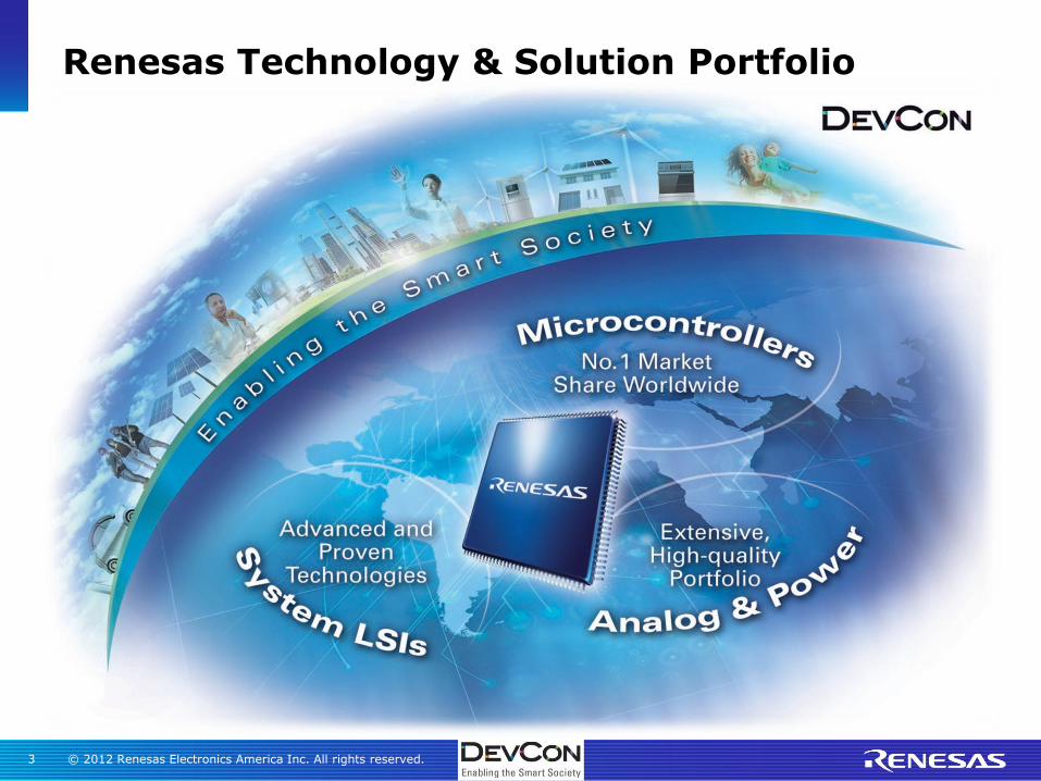
Renesas Technology & Solution Portfolio
© 2012 Renesas Electronics America Inc. All rights reserved. 4
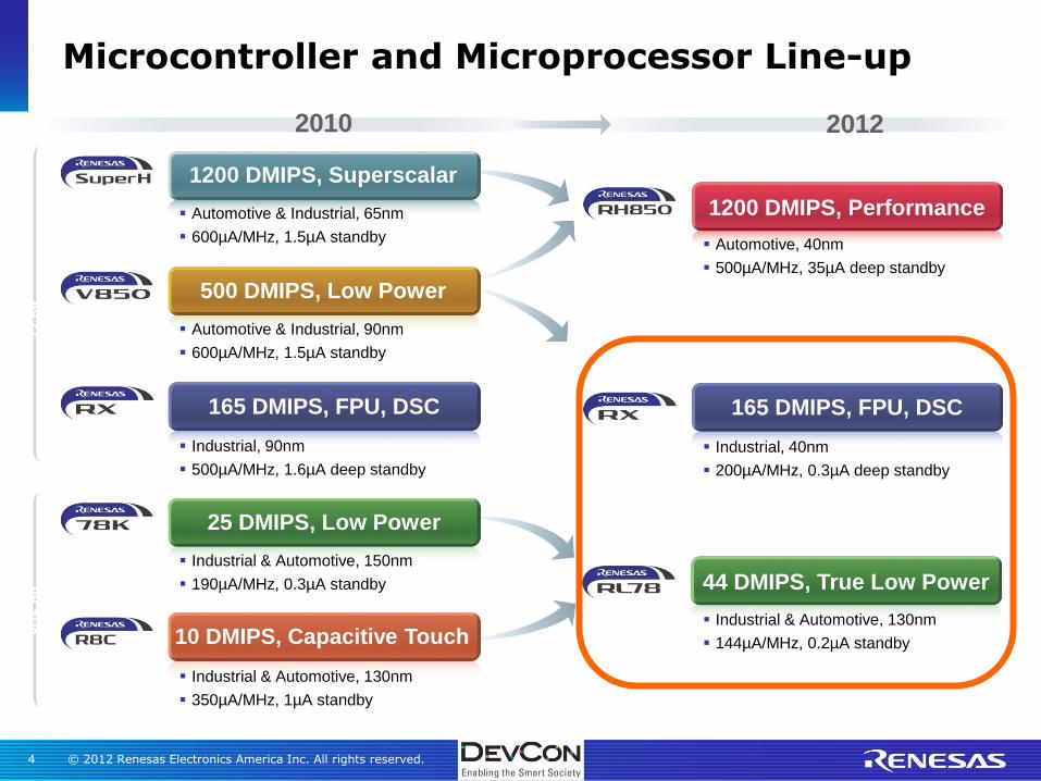
Microcontroller and Microprocessor Line-up
Wide Format LCDs Industrial & Automotive, 130nm
350µA/MHz, 1µA standby
44 DMIPS, True Low Power
165 DMIPS, FPU, DSC
1200 DMIPS, Performance
1200 DMIPS, Superscalar
500 DMIPS, Low Power
165 DMIPS, FPU, DSC
25 DMIPS, Low Power
10 DMIPS, Capacitive Touch
Industrial & Automotive, 150nm
190µA/MHz, 0.3µA standby
Industrial, 90nm
500µA/MHz, 1.6µA deep standby
Automotive & Industrial, 90nm
600µA/MHz, 1.5µA standby
Automotive & Industrial, 65nm
600µA/MHz, 1.5µA standby Automotive, 40nm
500µA/MHz, 35µA deep standby
Industrial, 40nm
200µA/MHz, 0.3µA deep standby
Industrial & Automotive, 130nm
144µA/MHz, 0.2µA standby
2010 2012
32-b
it
8/1
6-b
it
© 2012 Renesas Electronics America Inc. All rights reserved. 5
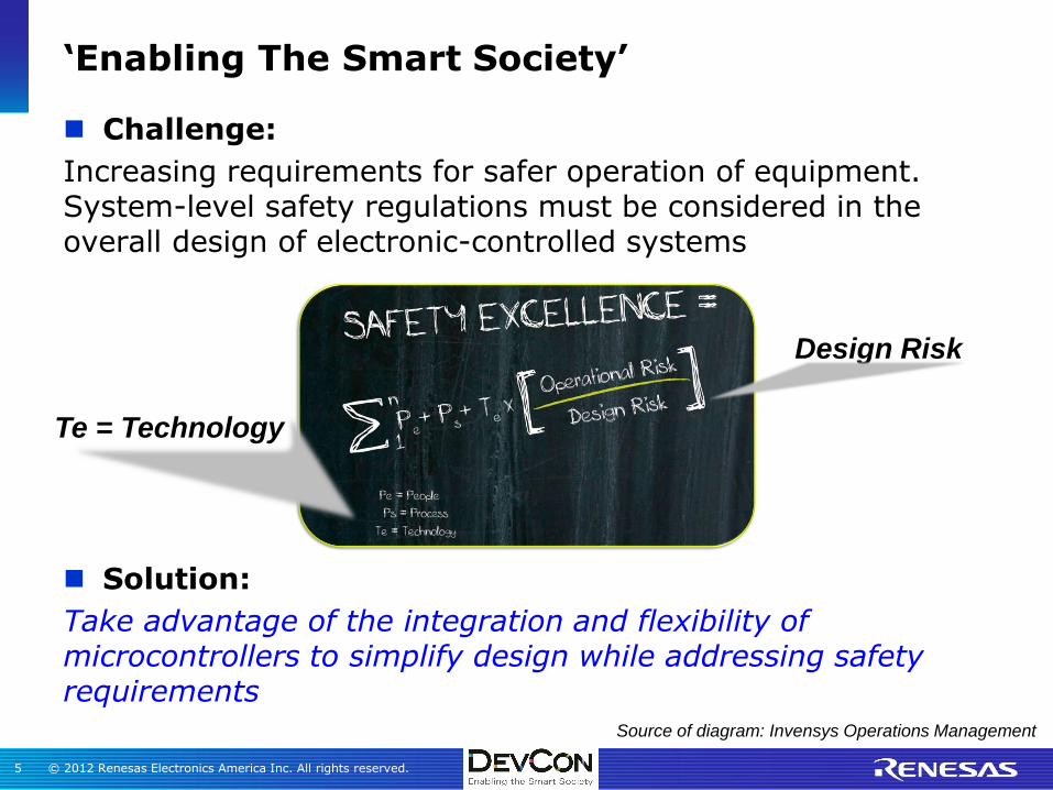
Challenge:
Increasing requirements for safer operation of equipment. System-level safety regulations must be considered in the overall design of electronic-controlled systems
Solution:
Take advantage of the integration and flexibility of microcontrollers to simplify design while addressing safety requirements
‘Enabling The Smart Society’
Te = Technology
Design Risk
Source of diagram: Invensys Operations Management
© 2012 Renesas Electronics America Inc. All rights reserved. 6
Introduction to safety
Use of microcontrollers for safer designs
Renesas support for safety standards
Summary
Q&A
Agenda
© 2012 Renesas Electronics America Inc. All rights reserved. 7
Introduction to Safety
© 2012 Renesas Electronics America Inc. All rights reserved. 8
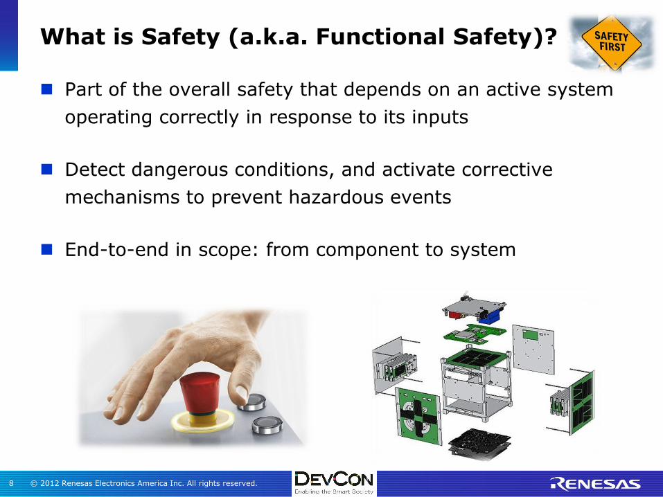
What is Safety (a.k.a. Functional Safety)?
Part of the overall safety that depends on an active system
operating correctly in response to its inputs
Detect dangerous conditions, and activate corrective
mechanisms to prevent hazardous events
End-to-end in scope: from component to system
© 2012 Renesas Electronics America Inc. All rights reserved. 9
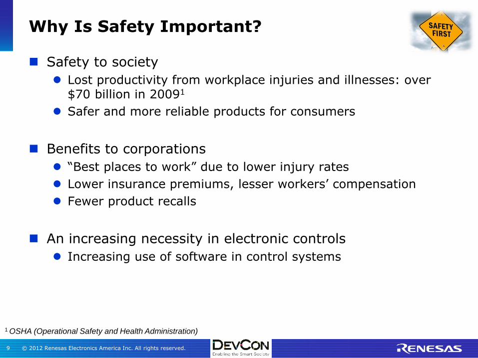
Why Is Safety Important?
Safety to society
Lost productivity from workplace injuries and illnesses: over $70 billion in 20091
Safer and more reliable products for consumers
Benefits to corporations
“Best places to work” due to lower injury rates
Lower insurance premiums, lesser workers’ compensation
Fewer product recalls
An increasing necessity in electronic controls
Increasing use of software in control systems
1 OSHA (Operational Safety and Health Administration)
© 2012 Renesas Electronics America Inc. All rights reserved. 10
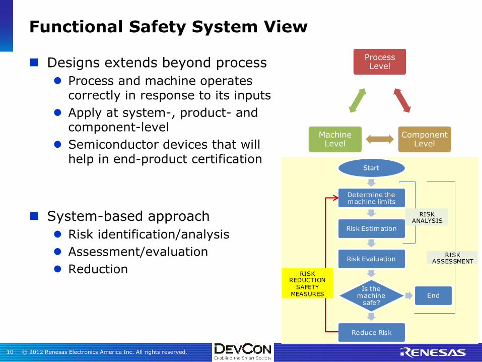
Functional Safety System View
Designs extends beyond process
Process and machine operates correctly in response to its inputs
Apply at system-, product- and component-level
Semiconductor devices that will help in end-product certification
System-based approach
Risk identification/analysis
Assessment/evaluation
Reduction
Process Level
Component Level
Machine Level
Start
Determine the machine limits
Risk Estimation
Risk Evaluation
Is the machine
safe?
Reduce Risk
End
RISK ANALYSIS
RISK ASSESSMENT
RISK REDUCTION
SAFETY MEASURES
© 2012 Renesas Electronics America Inc. All rights reserved. 11
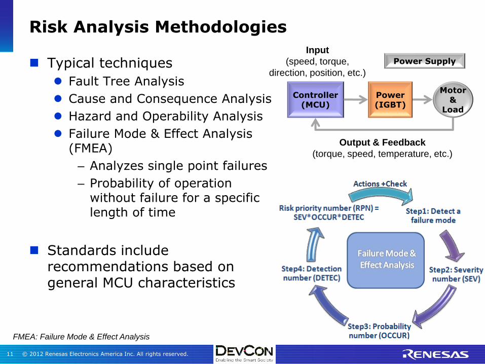
Risk Analysis Methodologies
Typical techniques
Fault Tree Analysis
Cause and Consequence Analysis
Hazard and Operability Analysis
Failure Mode & Effect Analysis (FMEA)
– Analyzes single point failures
– Probability of operation without failure for a specific length of time
Standards include recommendations based on general MCU characteristics
FMEA: Failure Mode & Effect Analysis
Controller (MCU)
Motor&
Load
Power (IGBT)
Output & Feedback
(torque, speed, temperature, etc.)
Input
(speed, torque,
direction, position, etc.)
Power Supply
© 2012 Renesas Electronics America Inc. All rights reserved. 12
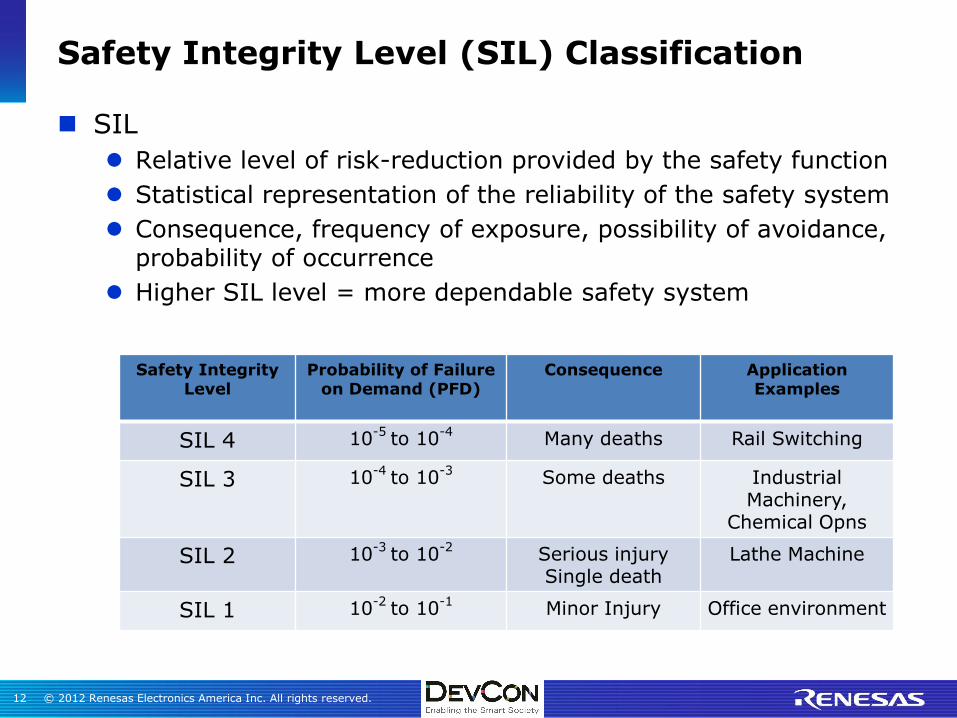
Safety Integrity Level (SIL) Classification
SIL
Relative level of risk-reduction provided by the safety function
Statistical representation of the reliability of the safety system
Consequence, frequency of exposure, possibility of avoidance, probability of occurrence
Higher SIL level = more dependable safety system
Safety Integrity Level
Probability of Failure on Demand (PFD)
Consequence Application Examples
SIL 4 10-5
to 10-4
Many deaths Rail Switching
SIL 3 10-4
to 10-3
Some deaths Industrial Machinery,
Chemical Opns
SIL 2 10-3
to 10-2
Serious injury Single death
Lathe Machine
SIL 1 10-2
to 10-1
Minor Injury Office environment
© 2012 Renesas Electronics America Inc. All rights reserved. 13
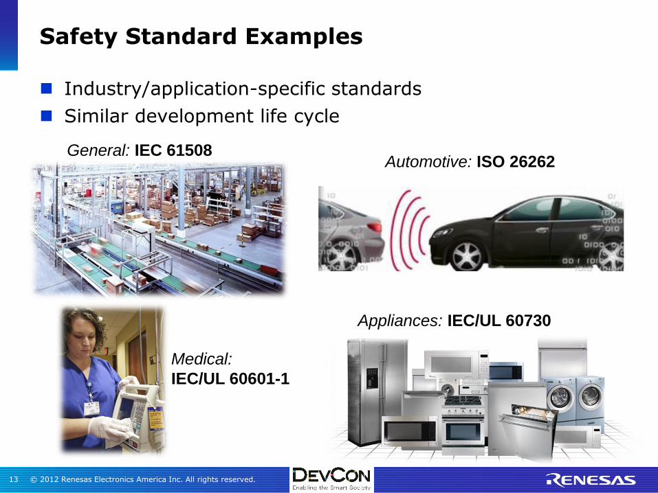
Safety Standard Examples
Industry/application-specific standards
Similar development life cycle
General: IEC 61508
Appliances: IEC/UL 60730
Medical:
IEC/UL 60601-1
Automotive: ISO 26262
© 2012 Renesas Electronics America Inc. All rights reserved. 14
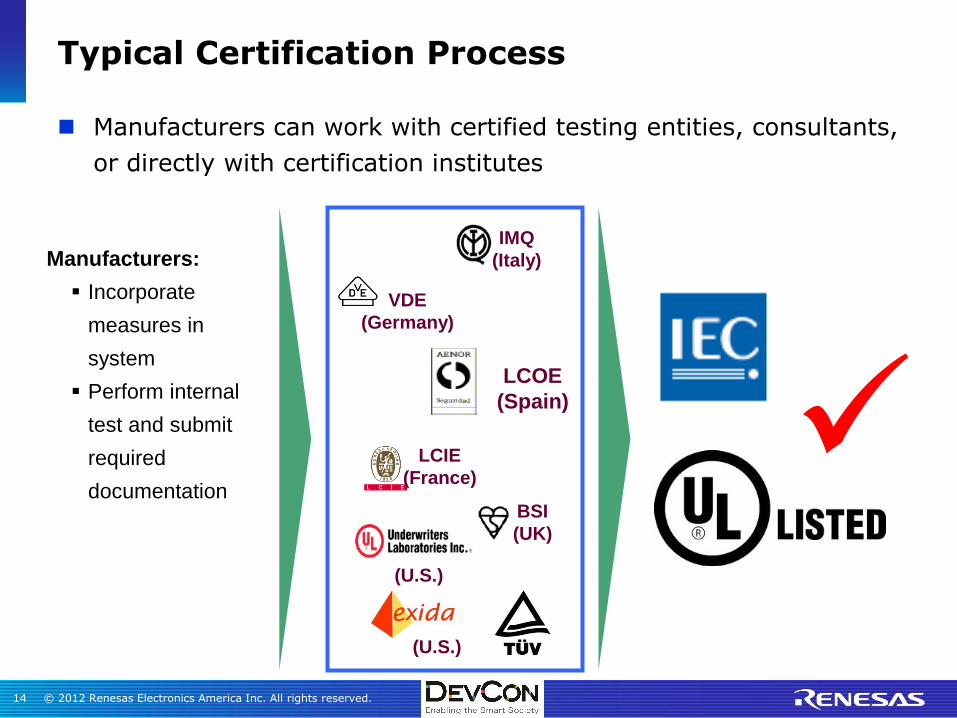
Typical Certification Process
Manufacturers can work with certified testing entities, consultants,
or directly with certification institutes
IMQ
(Italy)
VDE
(Germany)
BSI
(UK)
LCOE
(Spain)
LCIE
(France)
(U.S.)
Manufacturers:
Incorporate
measures in
system
Perform internal
test and submit
required
documentation
(U.S.)
© 2012 Renesas Electronics America Inc. All rights reserved. 15
Use of Microcontrollers for Safer Designs (ex: IEC 60730)
© 2012 Renesas Electronics America Inc. All rights reserved. 16
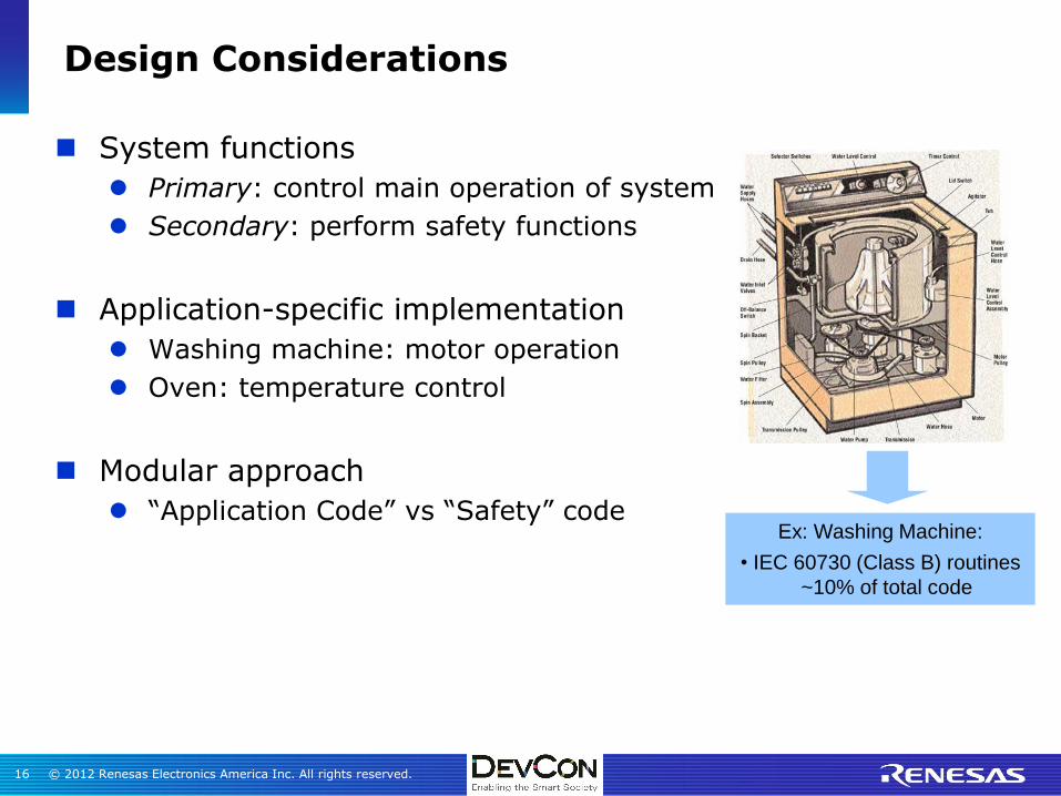
Design Considerations
System functions
Primary: control main operation of system
Secondary: perform safety functions
Application-specific implementation
Washing machine: motor operation
Oven: temperature control
Modular approach
“Application Code” vs “Safety” code Ex: Washing Machine:
• IEC 60730 (Class B) routines
~10% of total code
© 2012 Renesas Electronics America Inc. All rights reserved. 17
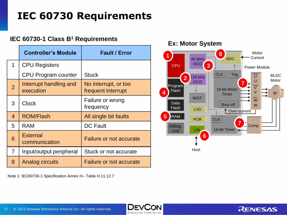
IEC 60730 Requirements
IEC 60730-1 Class B1 Requirements
16-bit Motor
Timer
LIN
Data
Flash Shut-off
ADC
WDT
125 kHz
OCO
CPU
16-bit Timer
Program
Flash
RAM
Comp.
CLK Trig
U
V
W
W
V
U
Power Module
BLDC
Motor
LVD
POR
Debug
Unit
40 MHz
OCO
Motor
Current
M
Over-current
CLK
1 CPU Registers
CPU Program counter Stuck
2 Interrupt handling and
execution
No interrupt, or too
frequent interrupt
3 Clock Failure or wrong
frequency
4 ROM/Flash All single bit faults
5 RAM DC Fault
6 External
communication Failure or not accurate
7 Input/output peripheral Stuck or not accurate
8 Analog circuits Failure or not accurate
Controller’s Module Fault / Error 1
Ex: Motor System
2
3
4
5
7
7
8
Note 1: IEC60730-1 Specification Annex H– Table H.11.12.7
6
Host
© 2012 Renesas Electronics America Inc. All rights reserved. 18
16-bit Motor
Timer
LIN
Data
Flash Shut-off
ADC
WDT
125 kHz
OCO
CPU
16-bit Timer
Program
Flash
RAM
CLK Trig
LVD
POR
Debug
Unit
40 MHz
OCO
CLK
1
FB
A1
A0
R3
R2
R1LR1HR3
R0LR0HR2
FB
A1
A0
R3
R2
R1LR1HR3
R0LR0HR2
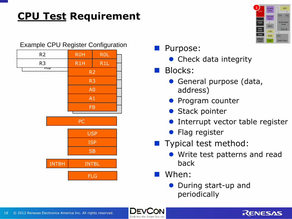
CPU Test Requirement
R2 R0H R0L
R3 R1H R1L
R2
R3
A0
A1
FB
USP
ISP
SB
INTBH INTBL
PC
FLG
Example CPU Register Configuration Purpose:
Check data integrity
Blocks:
General purpose (data, address)
Program counter
Stack pointer
Interrupt vector table register
Flag register
Typical test method:
Write test patterns and read back
When:
During start-up and periodically
16-bit Motor
Timer
LIN
Data
FlashShut-off
ADC
WDT
125 kHz
OCO
CPU
16-bit Timer
Program
Flash
RAM
CLK Trig
LVD
POR
Debug
Unit
40 MHz
OCO
CLK
16-bit Motor
Timer
LIN
Data
FlashShut-off
ADC
WDT
125 kHz
OCO
CPU
16-bit Timer
Program
Flash
RAM
CLK Trig
LVD
POR
Debug
Unit
40 MHz
OCO
CLK
1
© 2012 Renesas Electronics America Inc. All rights reserved. 19
16-bit Motor
Timer
LIN
Data
Flash Shut-off
ADC
WDT
125 kHz
OCO
CPU
16-bit Timer
Program
Flash
RAM
CLK Trig
LVD
POR
Debug
Unit
40 MHz
OCO
CLK
2
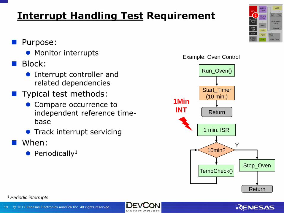
Interrupt Handling Test Requirement
Purpose:
Monitor interrupts
Block:
Interrupt controller and related dependencies
Typical test methods:
Compare occurrence to independent reference time-base
Track interrupt servicing
When:
Periodically1
1Min
INT
10min? Y
Start_Timer
(10 min.)
Run_Oven()
Stop_Oven
Return
TempCheck()
Example: Oven Control
16-bit Motor
Timer
LIN
Data
FlashShut-off
ADC
WDT
125 kHz
OCO
CPU
16-bit Timer
Program
Flash
RAM
CLK Trig
LVD
POR
Debug
Unit
40 MHz
OCO
CLK
16-bit Motor
Timer
LIN
Data
FlashShut-off
ADC
WDT
125 kHz
OCO
CPU
16-bit Timer
Program
Flash
RAM
CLK Trig
LVD
POR
Debug
Unit
40 MHz
OCO
CLK
2
Return
1 min. ISR
1 Periodic interrupts
© 2012 Renesas Electronics America Inc. All rights reserved. 20
16-bit Motor
Timer
LIN
Data
Flash Shut-off
ADC
WDT
125 kHz
OCO
CPU
16-bit Timer
Program
Flash
RAM
CLK Trig
LVD
POR
Debug
Unit
40 MHz
OCO
CLK
3
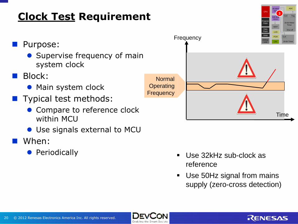
Clock Test Requirement
Purpose:
Supervise frequency of main system clock
Block:
Main system clock
Typical test methods:
Compare to reference clock within MCU
Use signals external to MCU
When:
Periodically
Frequency
Time
Normal
Operating
Frequency
Use 32kHz sub-clock as
reference
Use 50Hz signal from mains
supply (zero-cross detection)
16-bit Motor
Timer
LIN
Data
FlashShut-off
ADC
WDT
125 kHz
OCO
CPU
16-bit Timer
Program
Flash
RAM
CLK Trig
LVD
POR
Debug
Unit
40 MHz
OCO
CLK
16-bit Motor
Timer
LIN
Data
FlashShut-off
ADC
WDT
125 kHz
OCO
CPU
16-bit Timer
Program
Flash
RAM
CLK Trig
LVD
POR
Debug
Unit
40 MHz
OCO
CLK
3
© 2012 Renesas Electronics America Inc. All rights reserved. 21
16-bit Motor
Timer
LIN
Data
Flash Shut-off
ADC
WDT
125 kHz
OCO
CPU
16-bit Timer
Program
Flash
RAM
CLK Trig
LVD
POR
Debug
Unit
40 MHz
OCO
CLK
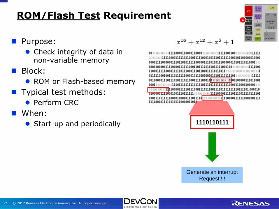
4
ROM/Flash Test Requirement
Purpose:
Check integrity of data in non-variable memory
Block:
ROM or Flash-based memory
Typical test methods:
Perform CRC
When:
Start-up and periodically 1110110111
Generate an interrupt
Request !!!
16-bit Motor
Timer
LIN
Data
FlashShut-off
ADC
WDT
125 kHz
OCO
CPU
16-bit Timer
Program
Flash
RAM
CLK Trig
LVD
POR
Debug
Unit
40 MHz
OCO
CLK
16-bit Motor
Timer
LIN
Data
FlashShut-off
ADC
WDT
125 kHz
OCO
CPU
16-bit Timer
Program
Flash
RAM
CLK Trig
LVD
POR
Debug
Unit
40 MHz
OCO
CLK
4
© 2012 Renesas Electronics America Inc. All rights reserved. 22
16-bit Motor
Timer
LIN
Data
Flash Shut-off
ADC
WDT
125 kHz
OCO
CPU
16-bit Timer
Program
Flash
RAM
CLK Trig
LVD
POR
Debug
Unit
40 MHz
OCO
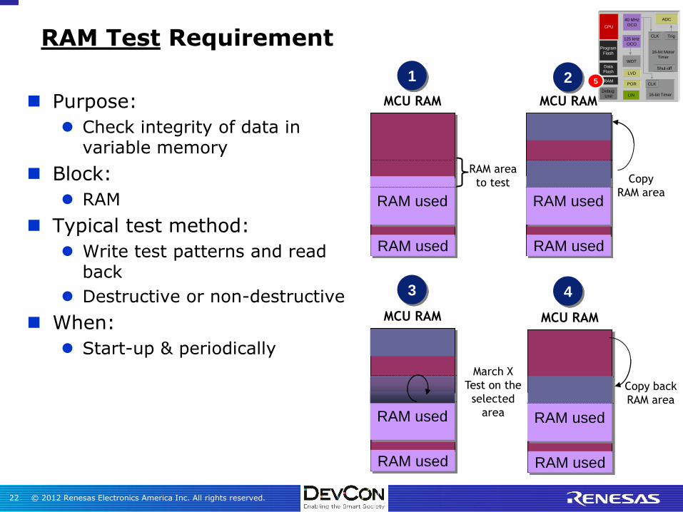
CLK 5
RAM Test Requirement
Purpose:
Check integrity of data in variable memory
Block:
RAM
Typical test method:
Write test patterns and read back
Destructive or non-destructive
When:
Start-up & periodically
MCU RAM
RAM used
2
RAM used
MCU RAM
RAM used
1
RAM used
RAM area
to test Copy
RAM area
MCU RAM
RAM used
3
RAM used
March X
Test on the
selected
area
MCU RAM
RAM used
4
RAM used
Copy back
RAM area
16-bit Motor
Timer
LIN
Data
FlashShut-off
ADC
WDT
125 kHz
OCO
CPU
16-bit Timer
Program
Flash
RAM
CLK Trig
LVD
POR
Debug
Unit
40 MHz
OCO
CLK
16-bit Motor
Timer
LIN
Data
FlashShut-off
ADC
WDT
125 kHz
OCO
CPU
16-bit Timer
Program
Flash
RAM
CLK Trig
LVD
POR
Debug
Unit
40 MHz
OCO
CLK5
© 2012 Renesas Electronics America Inc. All rights reserved. 23
16-bit Motor
Timer
LIN
Data
Flash Shut-off
ADC
WDT
125 kHz
OCO
CPU
16-bit Timer
Program
Flash
RAM
CLK Trig
LVD
POR
Debug
Unit
40 MHz
OCO
CLK
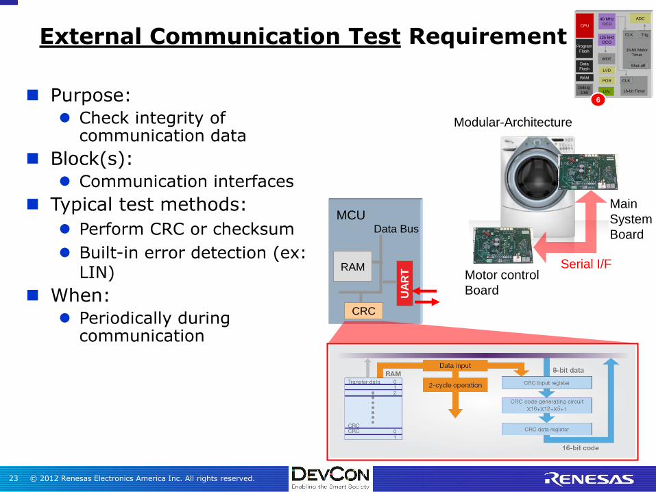
6
Main
System
Board
Motor control
Board
Serial I/F
Modular-Architecture
CRC
UA
RT
Data Bus
MCU
RAM
External Communication Test Requirement
Purpose: Check integrity of
communication data
Block(s): Communication interfaces
Typical test methods:
Perform CRC or checksum
Built-in error detection (ex: LIN)
When: Periodically during
communication
16-bit Motor
Timer
LIN
Data
FlashShut-off
ADC
WDT
125 kHz
OCO
CPU
16-bit Timer
Program
Flash
RAM
CLK Trig
LVD
POR
Debug
Unit
40 MHz
OCO
CLK
16-bit Motor
Timer
LIN
Data
FlashShut-off
ADC
WDT
125 kHz
OCO
CPU
16-bit Timer
Program
Flash
RAM
CLK Trig
LVD
POR
Debug
Unit
40 MHz
OCO
CLK
6
© 2012 Renesas Electronics America Inc. All rights reserved. 24
16-bit Motor
Timer
LIN
Data
Flash Shut-off
ADC
WDT
125 kHz
OCO
CPU
16-bit Timer
Program
Flash
RAM
CLK Trig
LVD
POR
Debug
Unit
40 MHz
OCO
CLK
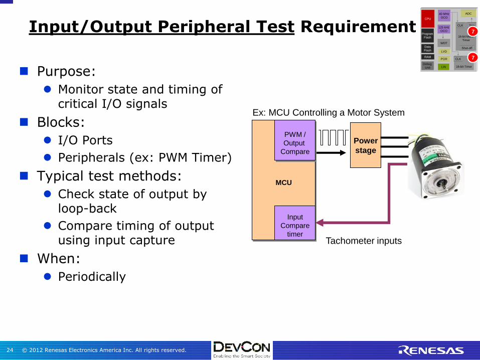
7
Input/Output Peripheral Test Requirement
Purpose:
Monitor state and timing of critical I/O signals
Blocks:
I/O Ports
Peripherals (ex: PWM Timer)
Typical test methods:
Check state of output by loop-back
Compare timing of output using input capture
When:
Periodically
MCU
Input
Compare
timer Tachometer inputs
Power
stage
PWM /
Output
Compare
Ex: MCU Controlling a Motor System
16-bit Motor
Timer
LIN
Data
FlashShut-off
ADC
WDT
125 kHz
OCO
CPU
16-bit Timer
Program
Flash
RAM
CLK Trig
LVD
POR
Debug
Unit
40 MHz
OCO
CLK
16-bit Motor
Timer
LIN
Data
FlashShut-off
ADC
WDT
125 kHz
OCO
CPU
16-bit Timer
Program
Flash
RAM
CLK Trig
LVD
POR
Debug
Unit
40 MHz
OCO
CLK 7
7
© 2012 Renesas Electronics America Inc. All rights reserved. 25
16-bit Motor
Timer
LIN
Data
Flash Shut-off
ADC
WDT
125 kHz
OCO
CPU
16-bit Timer
Program
Flash
RAM
CLK Trig
LVD
POR
Debug
Unit
40 MHz
OCO
CLK
8
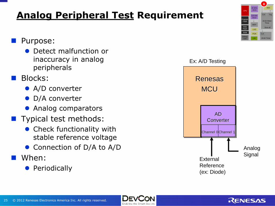
Analog Peripheral Test Requirement
Purpose:
Detect malfunction or inaccuracy in analog peripherals
Blocks:
A/D converter
D/A converter
Analog comparators
Typical test methods:
Check functionality with stable reference voltage
Connection of D/A to A/D
When:
Periodically
Renesas
MCU
AD
Converter
Channel 0 Channel 1
Analog
Signal External
Reference
(ex: Diode)
Ex: A/D Testing
16-bit Motor
Timer
LIN
Data
FlashShut-off
ADC
WDT
125 kHz
OCO
CPU
16-bit Timer
Program
Flash
RAM
CLK Trig
LVD
POR
Debug
Unit
40 MHz
OCO
CLK
16-bit Motor
Timer
LIN
Data
FlashShut-off
ADC
WDT
125 kHz
OCO
CPU
16-bit Timer
Program
Flash
RAM
CLK Trig
LVD
POR
Debug
Unit
40 MHz
OCO
CLK
8
© 2012 Renesas Electronics America Inc. All rights reserved. 26
Renesas Support for Safety Standards

© 2012 Renesas Electronics America Inc. All rights reserved. 27
Hardware Safety Features Example
Communication
SCI/UART
7 ch
SPI
USB
Analog
ADC 24bit ∆∑ + PGA
DAC
10-bit 2ch
Memory
Zero-Wait Flash
up to 1MB
SRAM
up to 128KB
Data Flash
up to 64KB
System
Data Mgmt.
DTC/DMA
Timers
MTU2
16-bit 6 ch
TMR
8-bit 4 ch
CMT
16-bit 4 ch
RTC Calendar
Temp. Sensor
Interrupt Contrl.
16 levels 9 pins
POR/LVD
Clock system
External Clock 20MHz
External Clock 32.768KHz
Internal LOCO 125KHz x 2
PLL
Multi-pin
Function Cont.
Event Link
Controller
Internal OCO Up to 50MHz
WDT
ADC 10-bit, 7ch
Comparator
4ch
I2C
7 x Simple I2C AES
Safety
Memory Protection
Unit (MPU)
ADC
Self-Diagnostics
Register
Write Protection
CRC
Safety
Independent
WDT
Clock Accuracy
Check (CAC)
Data Operating
Circuit (DOC)
Power Management
SLEEP, STOP,
STANDBY
External Bus
RX21A
© 2012 Renesas Electronics America Inc. All rights reserved. 28
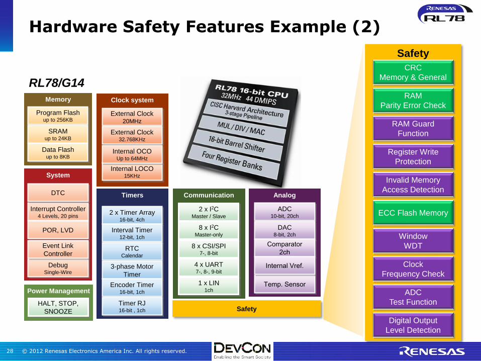
Hardware Safety Features Example (2)
Communication
2 x I2C Master / Slave
8 x I2C Master-only
8 x CSI/SPI 7-, 8-bit
4 x UART 7-, 8-, 9-bit
1 x LIN 1ch
Analog
ADC 10-bit, 20ch
Memory
Program Flash up to 256KB
SRAM up to 24KB
Data Flash up to 8KB
System
Interrupt Controller 4 Levels, 20 pins
Power Management
HALT, STOP,
SNOOZE
Timers
2 x Timer Array 16-bit, 4ch
Interval Timer 12-bit, 1ch
RTC Calendar
Temp. Sensor
Safety
RAM
Parity Error Check
POR, LVD
Debug Single-Wire
ADC
Test Function
Register Write
Protection
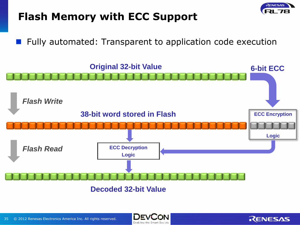
ECC Flash Memory
Clock system
External Clock 20MHz
External Clock 32.768KHz
Internal LOCO 15KHz
CRC
Memory & General
DTC
Internal OCO Up to 64MHz
3-phase Motor
Timer
Encoder Timer 16-bit, 1ch
Timer RJ 16-bit , 1ch
Event Link
Controller
DAC 8-bit, 2ch
Comparator
2ch
Internal Vref.
Safety
Window
WDT
Clock
Frequency Check
Invalid Memory
Access Detection
Digital Output
Level Detection
RAM Guard
Function
RL78/G14
© 2012 Renesas Electronics America Inc. All rights reserved. 29
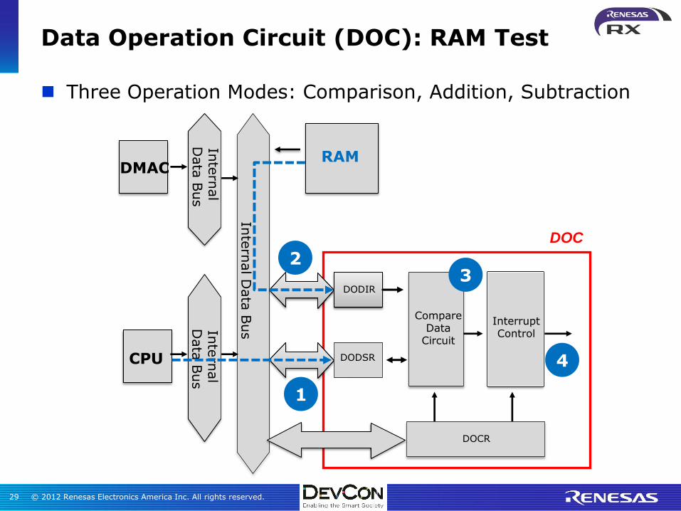
Inte
rnal D
ata
Bus
DODIR
DODSR
Compare Data
Circuit
Interrupt Control
DOCR
Inte
rnal
Data
Bus
Inte
rnal
Data
Bus
CPU
RAM DMAC
4
3 2
1
Data Operation Circuit (DOC): RAM Test
Three Operation Modes: Comparison, Addition, Subtraction
DOC
© 2012 Renesas Electronics America Inc. All rights reserved. 30
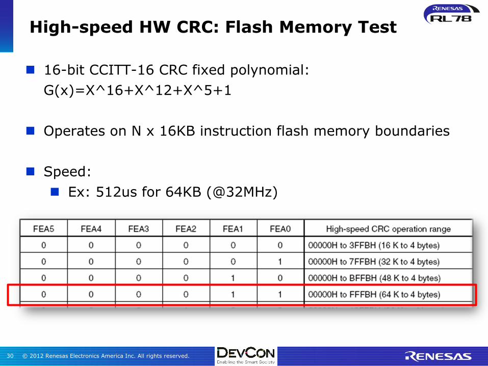
16-bit CCITT-16 CRC fixed polynomial:
G(x)=X^16+X^12+X^5+1
Operates on N x 16KB instruction flash memory boundaries
Speed:
Ex: 512us for 64KB (@32MHz)
High-speed HW CRC: Flash Memory Test
© 2012 Renesas Electronics America Inc. All rights reserved. 31
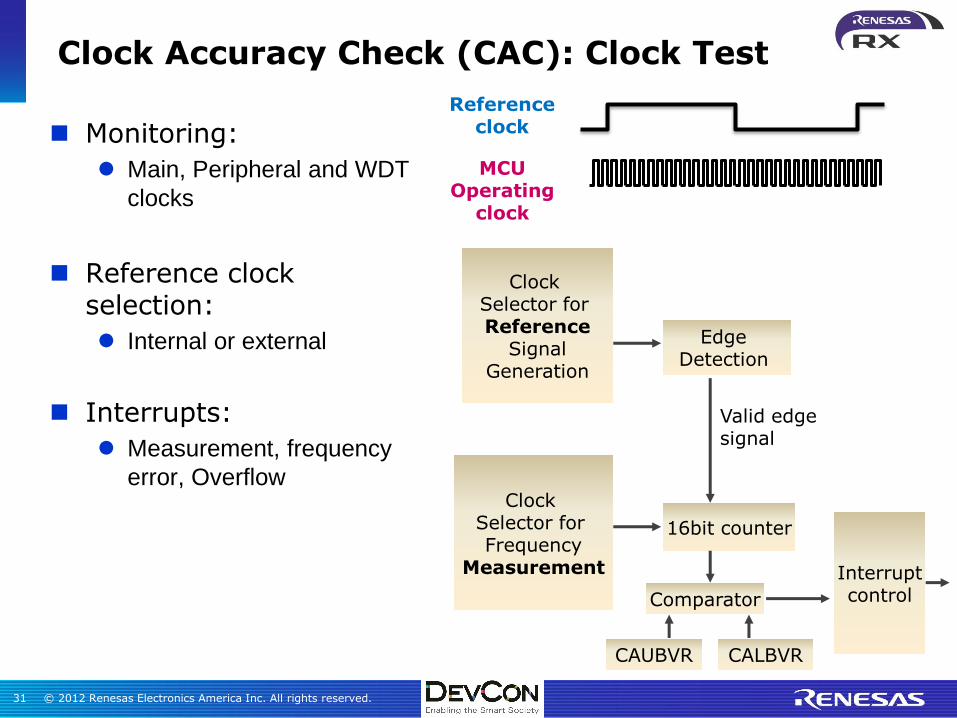
Clock Selector for Frequency
Measurement
Clock Selector for Reference
Signal Generation
16bit counter
Comparator
Interrupt control
Edge Detection
Valid edge signal
MCU Operating
clock
Reference clock
Monitoring:
Main, Peripheral and WDT
clocks
Reference clock selection:
Internal or external
Interrupts:
Measurement, frequency
error, Overflow
CAUBVR CALBVR
Clock Accuracy Check (CAC): Clock Test
© 2012 Renesas Electronics America Inc. All rights reserved. 32
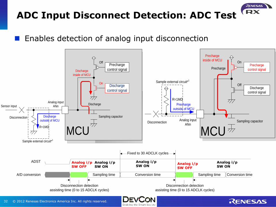
Precharge
control signal
Discharge
control signal
Analog input
ANn
Off
On
R=1MΩ
Disconnection Sampling capacitor
Sample external circuit*1
Discharge
Discharge
outside of MCU
Discharge
inside of MCU
MCU
Sensor input
Precharge
control signal
Discharge
control signal
Analog input
ANn
On
Off
R=1MΩ
Disconnection Sampling capacitor
Sample external circuit*1
Precharge
MCU
Precharge
inside of MCU
Precharge
outside of MCU
ADST
Fixed to 30 ADCLK cycles
A/D conversion Sampling time
Disconnection detection
assisting time (0 to 15 ADCLK cycles)
Conversion time Sampling time
Disconnection detection
assisting time (0 to 15 ADCLK cycles)
Conversion time
Analog i/p SW OFF
Analog i/p SW ON
Analog i/p SW ON
Analog i/p SW OFF
Analog i/p SW ON
ADC Input Disconnect Detection: ADC Test
Enables detection of analog input disconnection
© 2012 Renesas Electronics America Inc. All rights reserved. 33
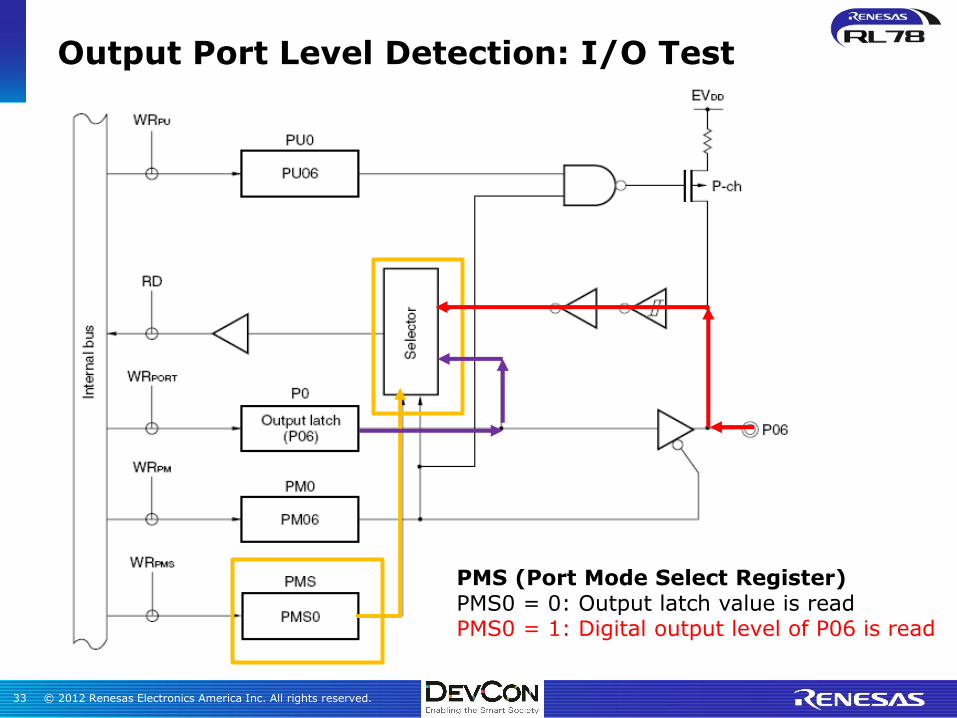
Output Port Level Detection: I/O Test
PMS (Port Mode Select Register) PMS0 = 0: Output latch value is read PMS0 = 1: Digital output level of P06 is read
© 2012 Renesas Electronics America Inc. All rights reserved. 34
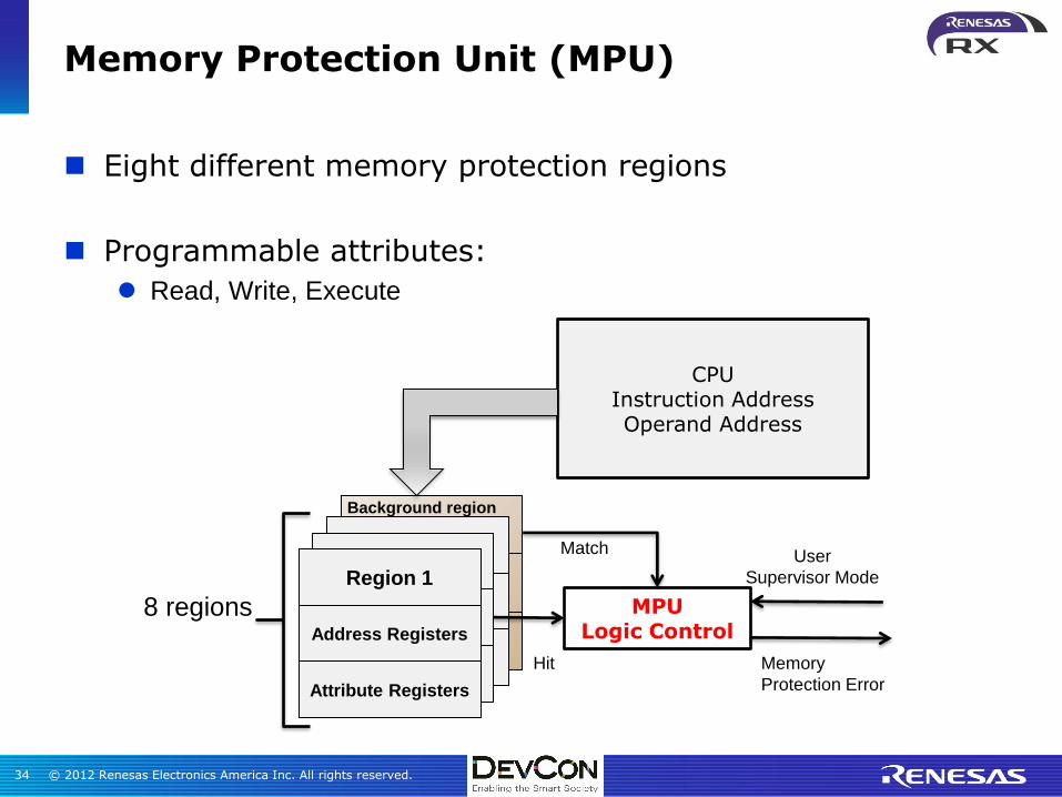
Memory Protection Unit (MPU)
Region 1
Address Registers
Attribute Registers
CPU Instruction Address Operand Address
MPU Logic Control
User
Supervisor Mode
Memory
Protection Error
Match
8 regions
Hit
Background region
Eight different memory protection regions
Programmable attributes:
Read, Write, Execute
© 2012 Renesas Electronics America Inc. All rights reserved. 35
Flash Memory with ECC Support
Fully automated: Transparent to application code execution
Original 32-bit Value 6-bit ECC
ECC Encryption
Logic
38-bit word stored in Flash
ECC Decryption
Logic
Decoded 32-bit Value
Flash Write
Flash Read
© 2012 Renesas Electronics America Inc. All rights reserved. 36
RAM Byte b7
b6
b5
b4
b3
b2
b1
b0
P
Addr 0 1 0 1 0 1 0 1 0
Addr + 1 0 1 1 1 1 1 1 1 1
Addr + 2 1 1 1 1 1 0 0 0 0
| . . . . . . . . .
| . . . . . . . . .
Addr + n 1 1 1 0 1 1 0 1 0
Addr + n + 1 1 1 1 1 1 1 1 1 1
Addr + n + 2 0 0 0 0 0 0 0 1 0
Addr x 1 0 1 0 1 0 1 0 1
- Parity calculated on Write
- Parity checked on Read,
Parity error
Single-bit error due to:
- EMI, ESD
- HW failure
RAM Parity Error Check
Fully automated: Transparent to application code execution
© 2012 Renesas Electronics America Inc. All rights reserved. 37
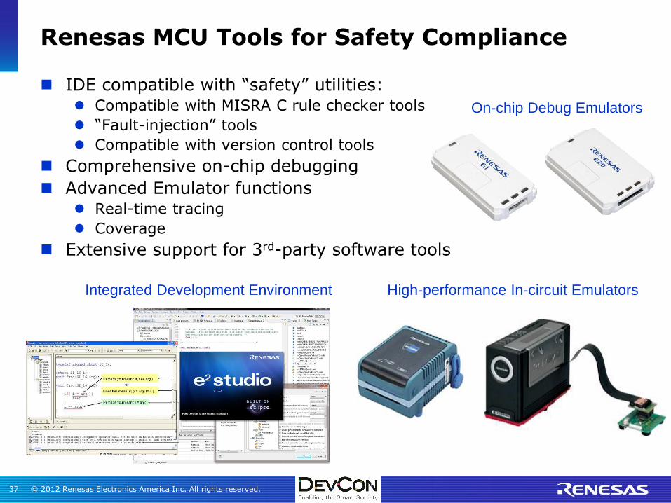
Renesas MCU Tools for Safety Compliance
IDE compatible with “safety” utilities: Compatible with MISRA C rule checker tools
“Fault-injection” tools
Compatible with version control tools
Comprehensive on-chip debugging
Advanced Emulator functions Real-time tracing
Coverage
Extensive support for 3rd-party software tools
Integrated Development Environment High-performance In-circuit Emulators
On-chip Debug Emulators
© 2012 Renesas Electronics America Inc. All rights reserved. 38
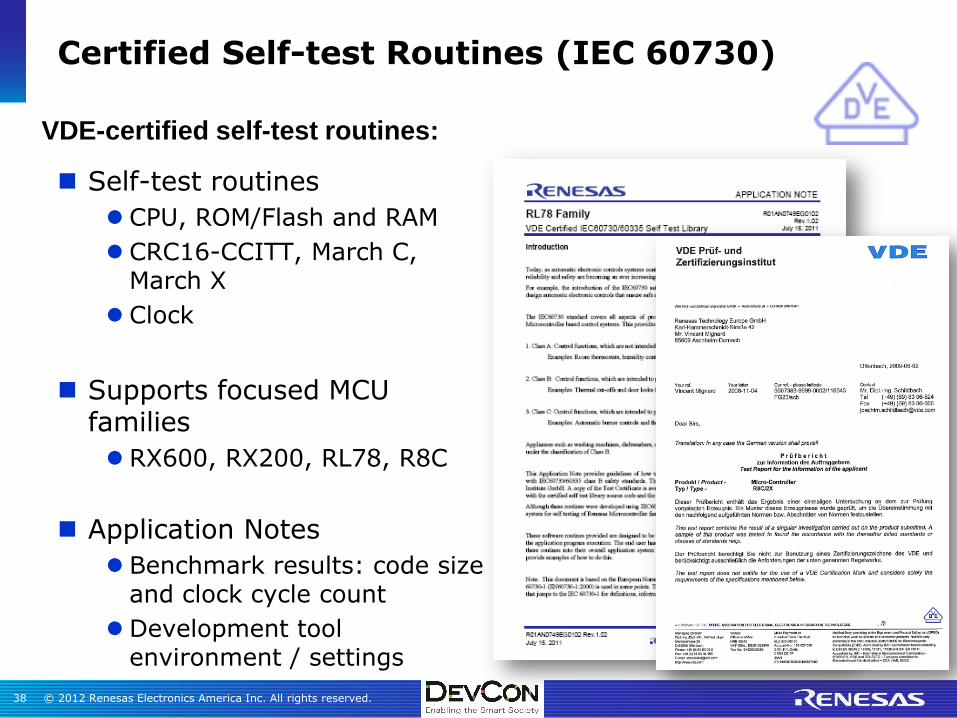
Certified Self-test Routines (IEC 60730)
Self-test routines
CPU, ROM/Flash and RAM
CRC16-CCITT, March C, March X
Clock
Supports focused MCU families
RX600, RX200, RL78, R8C
Application Notes
Benchmark results: code size and clock cycle count
Development tool environment / settings
VDE-certified self-test routines:
© 2012 Renesas Electronics America Inc. All rights reserved. 39
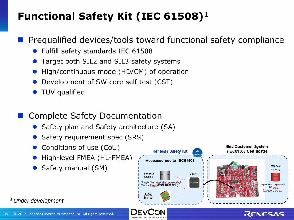
Prequalified devices/tools toward functional safety compliance
Fulfill safety standards IEC 61508
Target both SIL2 and SIL3 safety systems
High/continuous mode (HD/CM) of operation
Development of SW core self test (CST)
TUV qualified
Complete Safety Documentation
Safety plan and Safety architecture (SA)
Safety requirement spec (SRS)
Conditions of use (CoU)
High-level FMEA (HL-FMEA)
Safety manual (SM)
Functional Safety Kit (IEC 61508)1
1 Under development
© 2012 Renesas Electronics America Inc. All rights reserved. 40
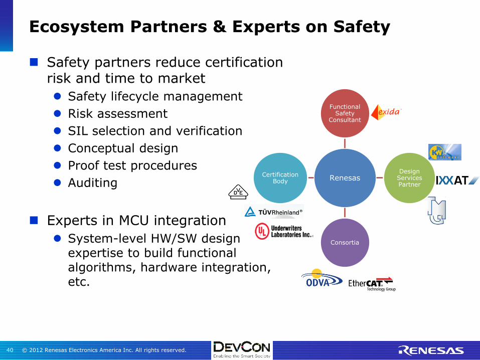
Ecosystem Partners & Experts on Safety
Safety partners reduce certification risk and time to market
Safety lifecycle management
Risk assessment
SIL selection and verification
Conceptual design
Proof test procedures
Auditing
Experts in MCU integration
System-level HW/SW design expertise to build functional algorithms, hardware integration, etc.
Renesas
Functional Safety
Consultant
Design Services Partner
Consortia
Certification Body
© 2012 Renesas Electronics America Inc. All rights reserved. 41
Growing need for higher safety
Different standards, similar design methodologies
Different ways to implement safety mechanisms
Renesas’ solutions to safety requirements:
Comprehensive device solutions with hardware-assisted safety features
Software and tools to help you design robust safety systems
Complete safety partner network reduces time to market and risk
Summary
© 2012 Renesas Electronics America Inc. All rights reserved. 42
Questions?
© 2012 Renesas Electronics America Inc. All rights reserved. 43
Challenge:
Increasing requirements for safer operation of equipment. System-level safety regulations must be considered in the overall design of electronic-controlled systems
Solution:
Take advantage of the integration and flexibility of Renesas microcontroller-based solutions to address safety requirements for a wide range of applications.
‘Enabling The Smart Society’

© 2012 Renesas Electronics America Inc. All rights reserved. 44
Please utilize the ‘Guidebook’ application to leave feedback
or
Ask me for the paper feedback form for you to use…
Please Provide Your Feedback…
Renesas Electronics America Inc.
© 2012 Renesas Electronics America Inc. All rights reserved.
© 2012 Renesas Electronics America Inc. All rights reserved. 46
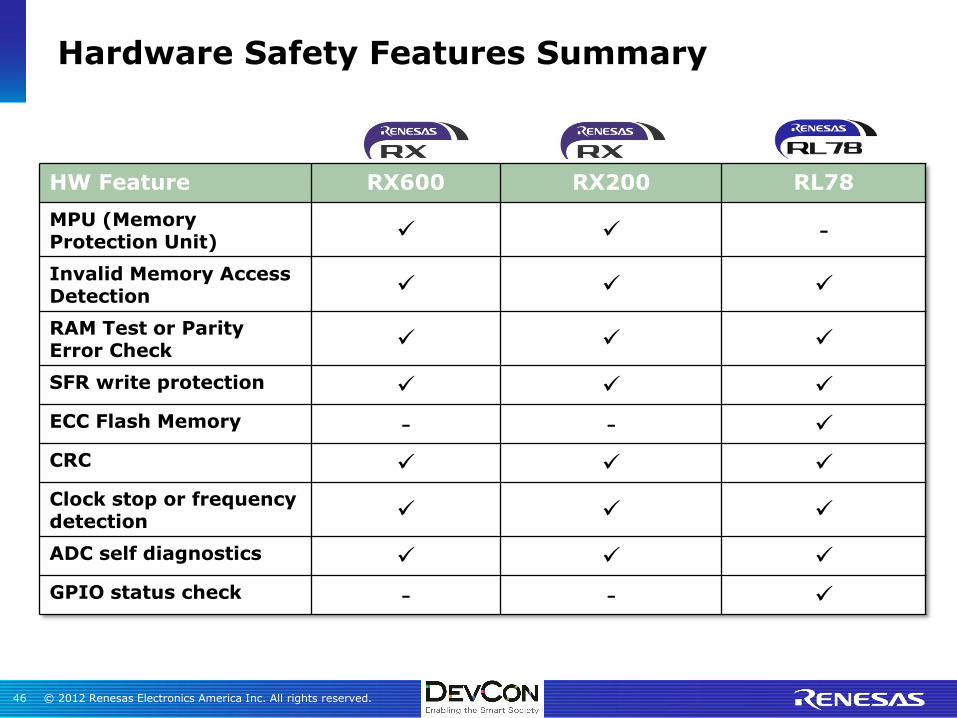
Hardware Safety Features Summary
HW Feature RX600 RX200 RL78
MPU (Memory Protection Unit)
-
Invalid Memory Access Detection
RAM Test or Parity Error Check
SFR write protection
ECC Flash Memory - -
CRC
Clock stop or frequency detection
ADC self diagnostics
GPIO status check - -
© 2012 Renesas Electronics America Inc. All rights reserved. 47
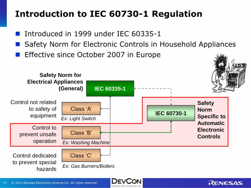
Introduction to IEC 60730-1 Regulation
Introduced in 1999 under IEC 60335-1
Safety Norm for Electronic Controls in Household Appliances
Effective since October 2007 in Europe
Class ‘A’
Control not related
to safety of
equipment Ex: Light Switch
Class ‘B’ Control to
prevent unsafe
operation Ex: Washing Machine
Class ‘C’ Control dedicated
to prevent special
hazards Ex: Gas Burners/Boilers
Safety
Norm
Specific to
Automatic
Electronic
Controls
IEC 60335-1
Safety Norm for
Electrical Appliances
(General)
IEC 60730-1
© 2012 Renesas Electronics America Inc. All rights reserved. 48
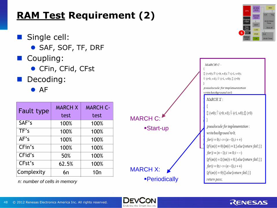
RAM Test Requirement (2)
Fault type MARCH X
test
MARCH C-
test
SAF’s 100% 100%
TF’s 100% 100%
AF’s 100% 100%
CFin’s 100% 100%
CFid’s 50% 100%
CFst’s 62.5% 100%
Complexity 6n 10n
16KB RAM
test timing9.6ms 16ms
MARCH C:
Start-up
MARCH X:
Periodically n: number of cells in memory
Single cell:
SAF, SOF, TF, DRF
Coupling:
CFin, CFid, CFst
Decoding:
AF
16-bit Motor
Timer
LIN
Data
FlashShut-off
ADC
WDT
125 kHz
OCO
CPU
16-bit Timer
Program
Flash
RAM
CLK Trig
LVD
POR
Debug
Unit
40 MHz
OCO
CLK
16-bit Motor
Timer
LIN
Data
FlashShut-off
ADC
WDT
125 kHz
OCO
CPU
16-bit Timer
Program
Flash
RAM
CLK Trig
LVD
POR
Debug
Unit
40 MHz
OCO
CLK5