Embed Size (px)
Citation preview

Microcontroller withUHF ASK/FSK Transmitter
ATA8743
9152B–INDCO–02/10
General Features• Transmitter with Microcontroller Consisting of an AVR® Microcontroller and RF
Transmitter PLL in a Single QFN24 5 mm × 5 mm Package (Pitch 0.65 mm)– f0 = 868 MHz to 928 MHz
• Temperature Range –40°C to +85°C• Supply Voltage 2.0V to 4.0V Allowing Usage of Single Li-cell Power Supply• Low Power Consumption
– Active Mode: Typical 9.8 mA at 3.0V and 4 MHz Microcontroller-clock– Power-down Mode: Typical 200 nA at 3.0V
• Modulation Scheme ASK/FSK• Integrated PLL Loop Filter• Output Power of 5.5 dBm at 868.3 MHz• Easy to Design-in Due to Excellent Isolation of the PLL from the PA and Power Supply• Single-ended Antenna Output with High Efficient Power Amplifier• Very Robust ESD Protection: HBM 2500V, MM100V, CDM 1000V• High Performance, Low Power AVR 8-bit Microcontroller, Similar to Popular ATtiny44• Well Known and Market-accepted RISC Architecture• Non-volatile Program and Data Memories
– 4 KBytes of In-system Programmable Program Memory Flash– 256 Bytes In-system Programmable EEPROM– 256 Bytes Internal SRAM
• Programming Lock for Self-programming Flash Program and EEPROM Data Security• Peripheral Features
– Two Timer/Counter, 8- and 16-bit Counters with Two PWM Channels on Both– 10-bit ADC– On-chip Analog Comparator– Programmable Watchdog Timer with Separate On-chip Oscillator– Universal Serial Interface (USI)
• Special Microcontroller Features– debugWIRE On-chip Debug System– In-system Programmable via SPI Port– External and Internal Interrupt Sources– Pin Change Interrupt on 12 Pins– Enhanced Power-on Reset Circuit– Programmable Brown-out Detection Circuit– Internal Calibrated Oscillator– On-chip Temperature Sensor
• 12 Programmable I/O Lines
1. General DescriptionThe ATA8743 is a highly flexible programmable transmitter containing the AVR micro-controller ATtiny44V and the UHF PLL transmitters in a small QFN24 5 mm × 5 mmpackage. This device is a member of a transmitter family covering several operatingfrequency ranges, which has been specifically developed for the demands of RFlow-cost data transmission systems with data rates of up to 32 kBit/s. Its primary appli-cations are in the areas of industrial/aftermarket Remote Keyless-Entry (RKE)systems, alarm, telemetering, energy metering systems, home automotion/entertain-ment and toys. The ATA8743 can be used in the frequency band of f0 = 868 MHz forASK or FSK data transmission.
Figure 1-1. ASK System Block Diagram
UHF ASK/FSKRemote Control Receiver
UHF ASK/FSKRemote Control Transmitter
ATA8743
Antenna
LoopAntenna
VS
VS
1 to 6 Micro-controllerDemod
VCC_RF
GND_RF
PA_ENABLE
ATtiny44V
ATA8403
ATA8205
ENABLE
Control
XTOPLL
VCOLNA
XTO
PA
VCO
f/4 PLL
Powerup/down
ANT1
ANT2
PXYS1
S1
S1
PXY
PXY
PXY
PXY
PXY
PXY
VDD
GND
PXY
PXY
PXY
PXY
PXY
VS
CLK
29152B–INDCO–02/10
ATA8743
ATA8743
Figure 1-2. FSK System Block Diagram
UHF ASK/FSKRemote Control Receiver
UHF ASK/FSKRemote Control Transmitter
ATA8743
Antenna
LoopAntenna
VS
VS
1 to 6 Micro-controllerDemod
VCC_RF
GND_RF
PA_ENABLE
ATtiny44V
ATA8403
ATA8205
ENABLE
Control
XTOPLL
VCOLNA
XTO
PA
VCO
f/4 PLL
Powerup/down
ANT1
ANT2
PXYS1
S1
S1
PXY
PXY
PXY
PXY
PXY
PXY
VDD
GND
PXY
PXY
PXY
PXY
PXY
CLK
VS
39152B–INDCO–02/10
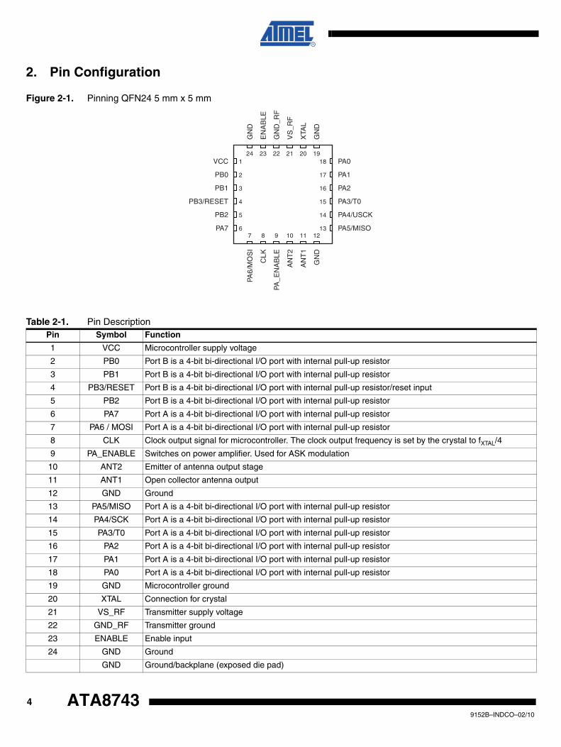
2. Pin Configuration
Figure 2-1. Pinning QFN24 5 mm x 5 mm
PB3/RESET
PB2
PA7
PB1
PB0
VCC
PA3/T0
PA4/USCK
PA5/MISO
PA2
PA1
PA0
VS
_RF
XTA
L
GN
D
GN
D_R
F
EN
AB
LE
GN
D
AN
T2
AN
T1
GN
D
PA_E
NA
BLE
CLK
PA6/
MO
SI
24
4
3
6
5
2
1
15
16
13
14
17
1823 22 21 20 19
7 8 9 10 11 12
Table 2-1. Pin DescriptionPin Symbol Function
1 VCC Microcontroller supply voltage
2 PB0 Port B is a 4-bit bi-directional I/O port with internal pull-up resistor
3 PB1 Port B is a 4-bit bi-directional I/O port with internal pull-up resistor
4 PB3/RESET Port B is a 4-bit bi-directional I/O port with internal pull-up resistor/reset input
5 PB2 Port B is a 4-bit bi-directional I/O port with internal pull-up resistor
6 PA7 Port A is a 4-bit bi-directional I/O port with internal pull-up resistor
7 PA6 / MOSI Port A is a 4-bit bi-directional I/O port with internal pull-up resistor
8 CLK Clock output signal for microcontroller. The clock output frequency is set by the crystal to fXTAL/4
9 PA_ENABLE Switches on power amplifier. Used for ASK modulation
10 ANT2 Emitter of antenna output stage
11 ANT1 Open collector antenna output
12 GND Ground
13 PA5/MISO Port A is a 4-bit bi-directional I/O port with internal pull-up resistor
14 PA4/SCK Port A is a 4-bit bi-directional I/O port with internal pull-up resistor
15 PA3/T0 Port A is a 4-bit bi-directional I/O port with internal pull-up resistor
16 PA2 Port A is a 4-bit bi-directional I/O port with internal pull-up resistor
17 PA1 Port A is a 4-bit bi-directional I/O port with internal pull-up resistor
18 PA0 Port A is a 4-bit bi-directional I/O port with internal pull-up resistor
19 GND Microcontroller ground
20 XTAL Connection for crystal
21 VS_RF Transmitter supply voltage
22 GND_RF Transmitter ground
23 ENABLE Enable input
24 GND Ground
GND Ground/backplane (exposed die pad)
49152B–INDCO–02/10
ATA8743
ATA8743
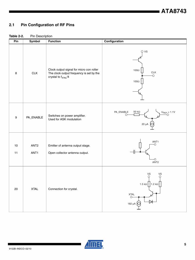
2.1 Pin Configuration of RF Pins
Table 2-2. Pin Description
Pin Symbol Function Configuration
8 CLKClock output signal for micro con rollerThe clock output frequency is set by the crystal to fXTAL/4
9 PA_ENABLESwitches on power amplifier.Used for ASK modulation
10
11
ANT2
ANT1
Emitter of antenna output stage.
Open collector antenna output.
20 XTAL Connection for crystal.
100Ω
100Ω CLK
VS
50 kΩ
20 µA
UREF = 1.1V PA_ENABLE
ANT1
ANT2
1.5 kΩ 1.2 kΩ
182 µA
XTAL
VS VS
59152B–INDCO–02/10
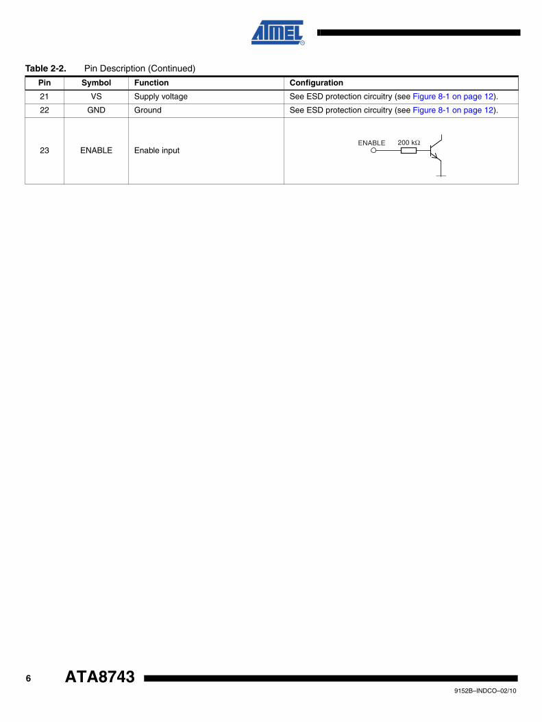
21 VS Supply voltage See ESD protection circuitry (see Figure 8-1 on page 12).
22 GND Ground See ESD protection circuitry (see Figure 8-1 on page 12).
23 ENABLE Enable input
Table 2-2. Pin Description (Continued)
Pin Symbol Function Configuration
200 kΩ ENABLE
69152B–INDCO–02/10
ATA8743
ATA8743
3. Functional DescriptionFor a typical application 3 to 4 interconnections between the AVR and the transmitter arerequired (see Figure 1-1 on page 2 and Figure 1-2 on page 3). The CLK line is used to allow themicrocontroller to generate an XTAL-based transmitter signal. The ENABLE line is used to startthe XTO, PLL, and clock output of the transmitter. The PA_ENABLE line is used to enable thepower amplifier in ASK and FSK mode. In FSK mode a fourth line is necessary to modulate theload capacity of the XTAL. To wake up the system from standby mode at least one key input isrequired. After pressing the key, the microcontroller starts up with the internal RC oscillator. ForTX operation user software must control ENABLE, PA_ENABLE, and XTAL load capacity asdescribed in the following section.
If ENABLE = L and PA_ENABLE = L the transmitter and the microcontroller (MCU) are instandby mode, reducing the power consumption so that a lithium cell can be used as power sup-ply for several years.
If ENABLE = H and PA_ENABLE = L, the XTO, PLL, and the CLK driver from the transmitter areactivated. The crystal oscillator together with the PLL from the RF transmitter typically requires< 1 ms until the PLL is locked and the clock output (Pin 8) is stable.
If ENABLE = H and PA_ENABLE = H, the XTO, PLL, CLK driver, and the power amplifier (PA)are switched on. ASK modulation is achieved by switching on and off the power amplifier viaPA_ENABLE. FSK modulation is achieved by switching on and off an additional capacitorbetween the XTAL load capacitor and GND, thus changing the reference frequency of the PLL.This is done using a MOS switch controlled by a microcontroller output. The power amplifier isswitched on via PA_ENABLE = H.
The MCU has to wait at least > 4 ms after setting ENABLE = H, before the external clock can beused. The external clock is connected via the timer0 input pin that clocks the USI from the MCUto achieve an accurate data transfer. The frequency of the internal RC oscillator is affected byambient temperature and operating voltage.
The USI provides two serial synchronous data transfer modes, with different physical I/O portsfor the data output. The two wire mode is used for ASK and the three wire mode is used for FSK.
If ENABLE = L and the PA_ENABLE = L, the circuit is in standby mode consuming only a verysmall amount of current, so that a lithium cell used as power supply can work for several years.
With ENABLE = H the XTO, PLL, and the CLK driver are switched on. If PA_ENABLE remains Lonly the PLL and the XTO are running and the CLK signal is delivered to the microcontroller.The VCO locks to 64 times the XTO frequency.
With ENABLE = H and PA_ENABLE = H the PLL, XTO, CLK driver, and the power amplifier areon. With PA_ENABLE the power amplifier can be switched on and off, which is used to performthe ASK modulation.
79152B–INDCO–02/10
3.1 Description of RF TransmitterThe integrated PLL transmitter is particularly suited to simple, low-cost applications. The VCO islocked to 64 × fXTAL hence a 13.5672 MHz crystal is needed for a 868.3 MHz transmitter and a14.2969 MHz crystal for a 915 MHz transmitter. All other PLL and VCO peripheral elements areintegrated.
The XTO is a series resonance oscillator so that only one capacitor together with a crystal con-nected in series to GND are needed as external elements.
The crystal oscillator together with the PLL typically need < 1 ms until the PLL is locked and theCLK output is stable. There is a wait time of ≥ 4 ms must be used until the CLK is used for themicrocontroller and the PA is switched on.
The power amplifier is an open-collector output delivering a current pulse, which is nearly inde-pendent from the load impedance. Thus, the delivered output power is controllable via theconnected load impedance.
This output configuration enables a simple matching to any kind of antenna or to 50Ω. Thisresults in a high power efficiency of η= Pout/(IS,PA × VS) of 24% for the power amplifier at868.3 MHz when an optimized load impedance of ZLoad = (166 + j226)Ω is used at 3V supplyvoltage.
3.2 ASK TransmissionThe RF TX block is activated by ENABLE = H. PA_ENABLE must remain L for t ≥ 4 ms, then theCLK signal is taken to clock the AVR and the output power can be modulated by means of pinPA_ENABLE. After transmission, PA_ENABLE is switched to L and the microcontroller switchesback to internal clocking. The RF TX is switched back to standby mode with ENABLE = L.
3.3 FSK TransmissionThe RF TX is activated by ENABLE = H. PA_ENABLE must remain L for t ≥ 4 ms, then the CLKsignal is taken to clock the AVR and the power amplifier is switched on with PA_ENABLE = H.The chip is then ready for FSK modulation. The AVR starts to switch on and off the capacitorbetween the XTAL load capacitor and GND with an open-drain output port, thus changing thereference frequency of the PLL. If the switch is closed, the output frequency is lower than if theswitch is open. After transmission PA_ENABLE is switched to L and the microcontroller switchesback to internal clocking. The RF TX is switched back to standby mode with ENABLE = L.
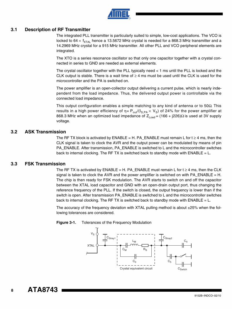
The accuracy of the frequency deviation with XTAL pulling method is about ±25% when the fol-lowing tolerances are considered.
Figure 3-1. Tolerances of the Frequency Modulation
RS
LM C4
CM
VS
XTAL
Crystal equivalent circuit
C0 C5
CSwitch
CStray1 CStray2
89152B–INDCO–02/10
ATA8743
ATA8743
Using C4 = 9.2 pF ±2%, C5 = 6.8 pF ±5%, a switch port with CSwitch = 3 pF ±10%, stray capaci-tances on each side of the crystal of CStray1 = CStray2 = 1 pF ±10%, a parallel capacitance of thecrystal of C0 = 3.2 pF ±10% and a crystal with CM = 13 fF ±10%, an FSK deviation of ±21.5 kHztypical with worst case tolerances of ±16.8 kHz to ±28.0 kHz results.
3.4 CLK OutputAn output CLK signal is provided for the integrated AVR. The delivered signal is CMOS compat-ible if the load capacitance is lower than 10 pF.
3.4.1 Clock Pulse Take-overThe clock of the crystal oscillator can be used for clocking the microcontroller. Atmel®’s AVRmicrocontroller starts with an integrated RC-oscillator to switch on the RF TX with ENABLE = H,and after 4 ms assumes the clock signal of the transmission IC, so that the message can be sentwith crystal accuracy.
3.4.2 Output Matching and Power SettingThe output power is set by the load impedance of the antenna. The maximum output power isachieved with a load impedance of ZLoad,opt = (166 + j226)Ω at 868.3 MHz. There must be a lowresistive path to VS to deliver the DC current.
The delivered current pulse of the power amplifier is 7.7 mA and the maximum output power isdelivered to a resistive load of 475Ω if the 0.53 pF output capacitance of the power amplifier iscompensated by the load impedance.
An optimum load impedance of:ZLoad = 475Ω || j/(2 × p × f × 0.53 pF) = (166 + j226)Ω is achieved for the maximum outputpower of 5.5 dBm.
The load impedance is defined as the impedance seen from the RF TX’s ANT1, ANT2 into thematching network. This large signal load impedance should not be confused with the small sig-nal input impedance delivered as input characteristic of RF amplifiers and measured from theapplication into the IC instead of from the IC into the application for a power amplifier.
Less output power is achieved by lowering the real parallel part of 475Ω where the parallel imag-inary part should be kept constant.
Output power measurement can be done using the circuit shown in Figure 8-4 on page 16. Notethat the component values must be changed to compensate the individual board parasitics untilthe RF TX has the right load impedance ZLoad,opt = (166 + j226)Ω at 868.3 MHz. In addition, thedamping of the cable used to measure the output power must be calibrated out.
4. Microcontroller BlockMore detailed information about the microcontroller block can be found in the appendix.
99152B–INDCO–02/10
5. Absolute Maximum RatingsStresses beyond those listed under “Absolute Maximum Ratings” may cause permanent damage to the device. This is a stress rating only and functional operation of the device at these or any other conditions beyond those indicated in the operational sections of this specification is not implied. Exposure to absolute maximum rating conditions for extended periods may affect device reliability.
Parameters Symbol Minimum Maximum Unit
Supply voltage VS 5 V
Power dissipation Ptot 100 mW
Junction temperature Tj 150 °C
Storage temperature Tstg –55 125 °C
Ambient temperature Tamb –55 125 °C
Input voltage VmaxPA_ENABLE –0.3 (VS + 0.3)(1) V
Note: 1. If VS + 0.3 is higher than 3.7V, the maximum voltage will be reduced to 3.7V.
6. Thermal ResistanceParameters Symbol Value Unit
Junction ambient RthJA 170 K/W
7. Electrical CharacteristicsVS = 2.0V to 4.0V, Tamb = 25°C unless otherwise specified. Typical values are given at VS = 3.0V and Tamb = 25°C. All parameters are referred to GND (pin 7).
Parameters Test Conditions Symbol Min. Typ. Max. Unit
Supply current Power down, microcontroller Watchdog timer disabled
IS_Off210
24.35nAµA
Supply current Power up, 4 MHz internal RC oscillator IS_Transmit 9.3 mA
Output powerVS = 3.0V, Tamb = 25°C,f = 868.3 MHz, ZLoad = (166 + j226)Ω PRef 3.5 5.5 8 dBm
Output power variation for the full temperature range
Tamb = 25°C,VS = 3.0VVS = 2.0V
ΔPRefΔPRef
–1.5–4.0
dBdB
Output power variation for the full temperature range
Tamb = 25°C,VS = 3.0VVS = 2.0V, POut = PRef + ΔPRef
ΔPRefΔPRef
–2.0–4.5
dBdB
Achievable output-power range Selectable by load impedance POut_typ –3 +5.5 dBm
Spurious emission
fCLK = f0/128Load capacitance at pin CLK = 10 pFfO ±1 × fCLK fO ±4 × fCLK other spurious are lower
–52–52
dBcdBc
Oscillator frequency XTO (= phase comparator frequency)
fXTO = f0/64fXTAL = resonant frequency of the XTAL, CM ≤ 10 fF, load capacitance selected accordingly Tamb = 25°C,
fXTO
–30 fXTAL +30 ppm
PLL loop bandwidth 250 kHz
Note: 1. If VS is higher than 3.6V, the maximum voltage will be reduced to 3.6V.
109152B–INDCO–02/10
ATA8743
ATA8743
Phase noise of phase comparatorReferred to fPC = fXT0,25 kHz distance to carrier
–116 –110 dBc/Hz
In-loop phase noise PLL 25 kHz distance to carrier –80 –74 dBc/Hz
Phase noise VCOat 1 MHzat 36 MHz
–89–120
–86–117
dBc/HzdBc/Hz
Frequency range of VCO fVCO 868 928 MHz
Clock output frequency (CMOS microcontroller compatible)
f0/256 MHz
Voltage swing at pin CLK CLoad ≤ 10 pFV0hV0l
VS × 0.8VS × 0.2
VV
Series resonance R of the crystal Rs 110 Ω
Capacitive load at pin XT0 7 pF
FSK modulation frequency rate Duty cycle of the modulation signal = 50% 0 32 kHz
ASK modulation frequency rate Duty cycle of the modulation signal = 50% 0 32 kHz
ENABLE inputLow level input voltageHigh level input voltageInput current high
VIlVIhIIn
1.70.25
20
VVµA
PA_ENABLE inputLow level input voltageHigh level input voltageInput current high
VIlVIhIIn
1.70.25VS
(1)
5
VVµA
7. Electrical Characteristics (Continued)VS = 2.0V to 4.0V, Tamb = 25°C unless otherwise specified. Typical values are given at VS = 3.0V and Tamb = 25°C. All parameters are referred to GND (pin 7).
Parameters Test Conditions Symbol Min. Typ. Max. Unit
Note: 1. If VS is higher than 3.6V, the maximum voltage will be reduced to 3.6V.
119152B–INDCO–02/10
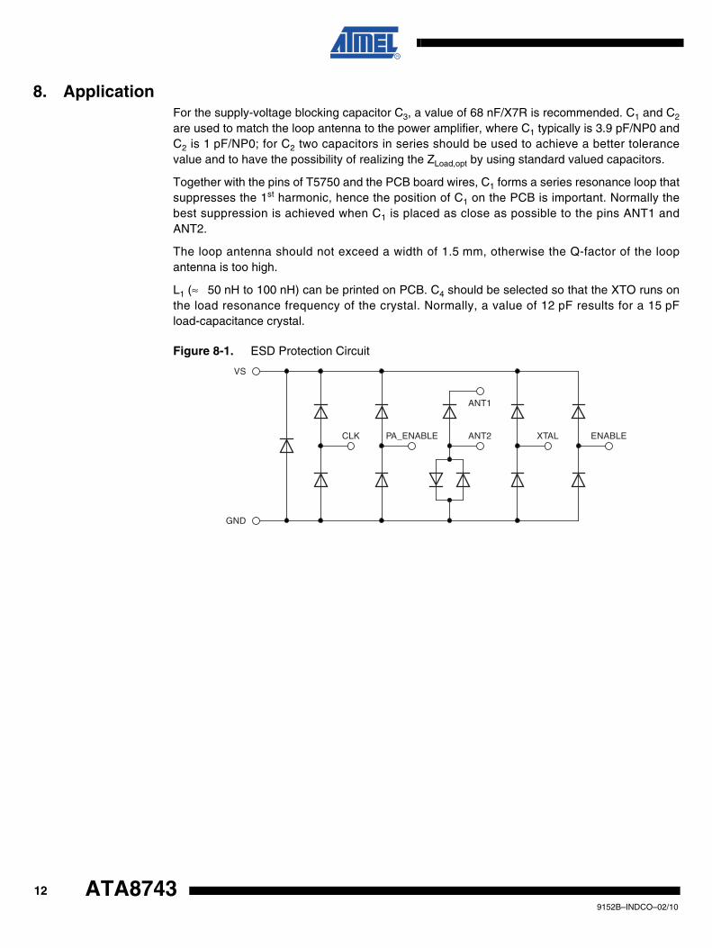
8. ApplicationFor the supply-voltage blocking capacitor C3, a value of 68 nF/X7R is recommended. C1 and C2
are used to match the loop antenna to the power amplifier, where C1 typically is 3.9 pF/NP0 andC2 is 1 pF/NP0; for C2 two capacitors in series should be used to achieve a better tolerancevalue and to have the possibility of realizing the ZLoad,opt by using standard valued capacitors.
Together with the pins of T5750 and the PCB board wires, C1 forms a series resonance loop thatsuppresses the 1st harmonic, hence the position of C1 on the PCB is important. Normally thebest suppression is achieved when C1 is placed as close as possible to the pins ANT1 andANT2.
The loop antenna should not exceed a width of 1.5 mm, otherwise the Q-factor of the loopantenna is too high.
L1 (≈ 50 nH to 100 nH) can be printed on PCB. C4 should be selected so that the XTO runs onthe load resonance frequency of the crystal. Normally, a value of 12 pF results for a 15 pFload-capacitance crystal.
Figure 8-1. ESD Protection Circuit
CLK
VS
GND
PA_ENABLE XTALANT2 ENABLE
ANT1
129152B–INDCO–02/10
ATA8743
ATA8743
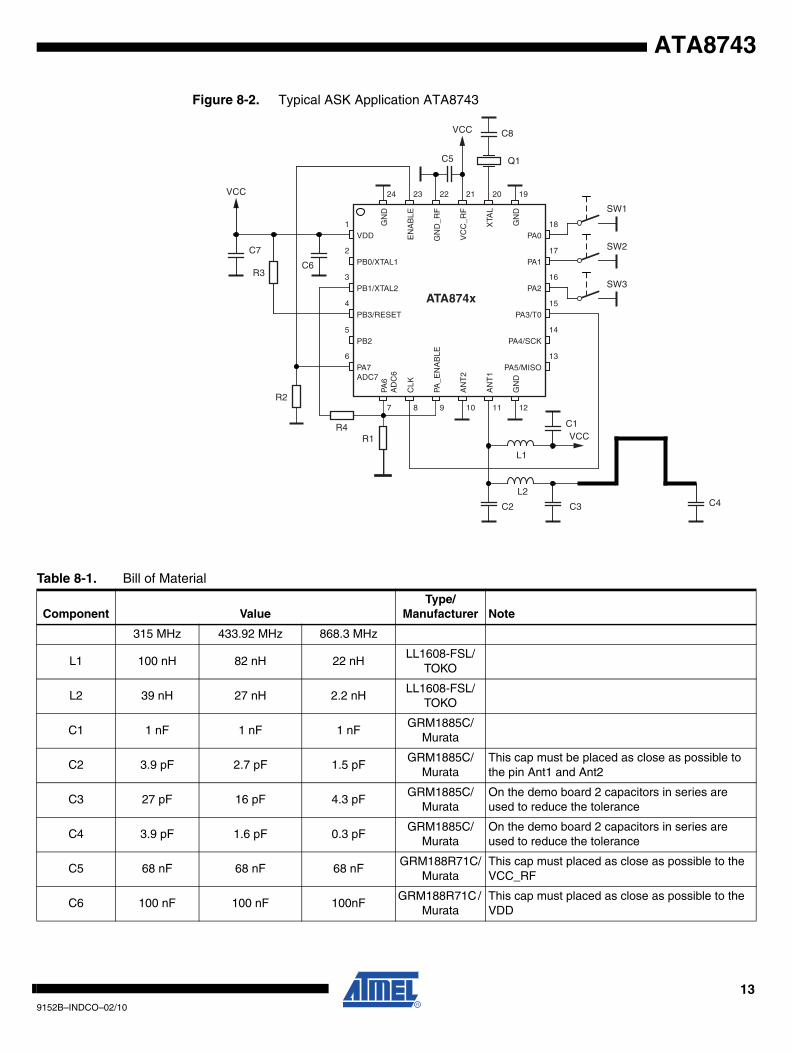
Figure 8-2. Typical ASK Application ATA8743
PB0/XTAL1
VDD
PB3/RESET
PB2
PA7ADC7
GN
D_R
F
GN
D
XTA
L
VC
C_R
F
EN
AB
LE
GN
D
PA_E
NA
BLE
GN
D
AN
T1
AN
T2
CLK
PA6
AD
C6
PB1/XTAL2
PA1
PA0
13
14
15
16
17
18
6
5
4
3
2
1
20 1922 2124 23
11 129 107 8
PA3/T0
PA4/SCK
PA5/MISO
PA2
C5
VCC
VCC
VCC
L1
ATA874x
SW1
SW3
SW2
C8
Q1
C6R3
C7
R2
R4R1
C4C3C2
L2
C1
Table 8-1. Bill of Material
Component ValueType/
Manufacturer Note
315 MHz 433.92 MHz 868.3 MHz
L1 100 nH 82 nH 22 nHLL1608-FSL/
TOKO
L2 39 nH 27 nH 2.2 nHLL1608-FSL/
TOKO
C1 1 nF 1 nF 1 nFGRM1885C/
Murata
C2 3.9 pF 2.7 pF 1.5 pFGRM1885C/
MurataThis cap must be placed as close as possible to the pin Ant1 and Ant2
C3 27 pF 16 pF 4.3 pFGRM1885C/
MurataOn the demo board 2 capacitors in series are used to reduce the tolerance
C4 3.9 pF 1.6 pF 0.3 pF GRM1885C/
MurataOn the demo board 2 capacitors in series are used to reduce the tolerance
C5 68 nF 68 nF 68 nFGRM188R71C/
MurataThis cap must placed as close as possible to the VCC_RF
C6 100 nF 100 nF 100nFGRM188R71C /
MurataThis cap must placed as close as possible to the VDD
139152B–INDCO–02/10
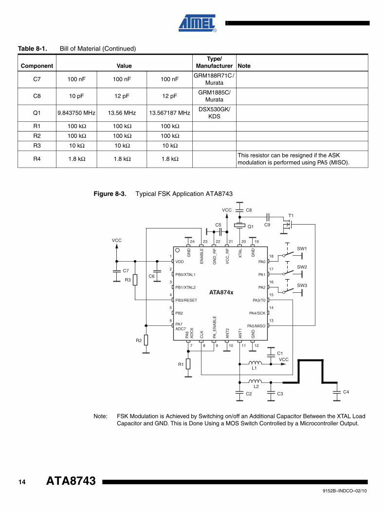
Figure 8-3. Typical FSK Application ATA8743
Note: FSK Modulation is Achieved by Switching on/off an Additional Capacitor Between the XTAL Load Capacitor and GND. This is Done Using a MOS Switch Controlled by a Microcontroller Output.
C7 100 nF 100 nF 100 nFGRM188R71C /
Murata
C8 10 pF 12 pF 12 pFGRM1885C/
Murata
Q1 9.843750 MHz 13.56 MHz 13.567187 MHzDSX530GK/
KDS
R1 100 kΩ 100 kΩ 100 kΩ
R2 100 kΩ 100 kΩ 100 kΩ
R3 10 kΩ 10 kΩ 10 kΩ
R4 1.8 kΩ 1.8 kΩ 1.8 kΩ This resistor can be resigned if the ASK modulation is performed using PA5 (MISO).
Table 8-1. Bill of Material (Continued)
Component ValueType/
Manufacturer Note
PB0/XTAL1
VDD
PB3/RESET
PB2
PA7ADC7
GN
D_R
F
GN
D
XTA
L
VC
C_R
F
EN
AB
LE
GN
D
PA_E
NA
BLE
GN
D
AN
T1
AN
T2
CLK
PA6
AD
C6
PB1/XTAL2
PA1
PA0
13
14
15
16
17
18
6
5
4
3
2
1
20 1922 2124 23
11 129 107 8
PA3/T0
PA4/SCK
PA5/MISO
PA2
C5
VCC
VCC
VCC
ATA874x
SW1
SW3
SW2
T1
C9Q1
C8
C6C7
R3
R2
R1
C4C3C2
L1
L2
C1
149152B–INDCO–02/10
ATA8743
ATA8743
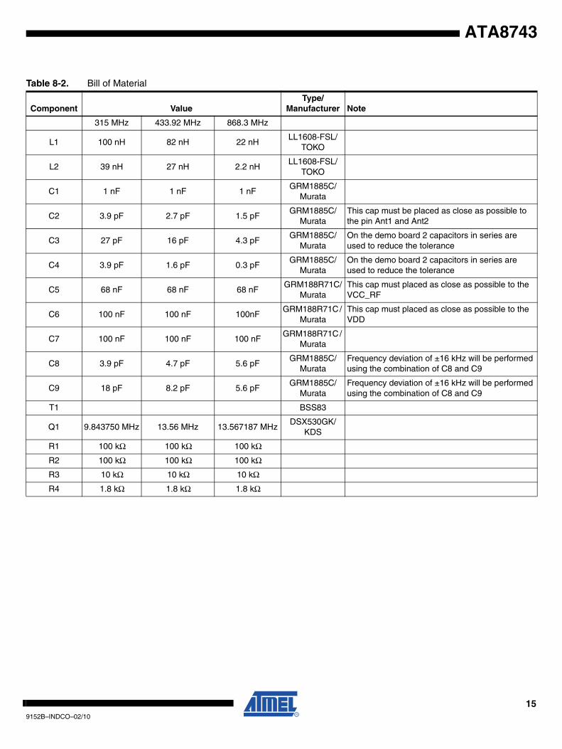
Table 8-2. Bill of Material
Component ValueType/
Manufacturer Note
315 MHz 433.92 MHz 868.3 MHz
L1 100 nH 82 nH 22 nHLL1608-FSL/
TOKO
L2 39 nH 27 nH 2.2 nHLL1608-FSL/
TOKO
C1 1 nF 1 nF 1 nFGRM1885C/
Murata
C2 3.9 pF 2.7 pF 1.5 pFGRM1885C/
MurataThis cap must be placed as close as possible to the pin Ant1 and Ant2
C3 27 pF 16 pF 4.3 pFGRM1885C/
MurataOn the demo board 2 capacitors in series are used to reduce the tolerance
C4 3.9 pF 1.6 pF 0.3 pF GRM1885C/
MurataOn the demo board 2 capacitors in series are used to reduce the tolerance
C5 68 nF 68 nF 68 nFGRM188R71C/
MurataThis cap must placed as close as possible to the VCC_RF
C6 100 nF 100 nF 100nFGRM188R71C /
MurataThis cap must placed as close as possible to the VDD
C7 100 nF 100 nF 100 nFGRM188R71C /
Murata
C8 3.9 pF 4.7 pF 5.6 pFGRM1885C/
MurataFrequency deviation of ±16 kHz will be performed using the combination of C8 and C9
C9 18 pF 8.2 pF 5.6 pFGRM1885C/
MurataFrequency deviation of ±16 kHz will be performed using the combination of C8 and C9
T1 BSS83
Q1 9.843750 MHz 13.56 MHz 13.567187 MHzDSX530GK/
KDS
R1 100 kΩ 100 kΩ 100 kΩ
R2 100 kΩ 100 kΩ 100 kΩ
R3 10 kΩ 10 kΩ 10 kΩ
R4 1.8 kΩ 1.8 kΩ 1.8 kΩ
159152B–INDCO–02/10
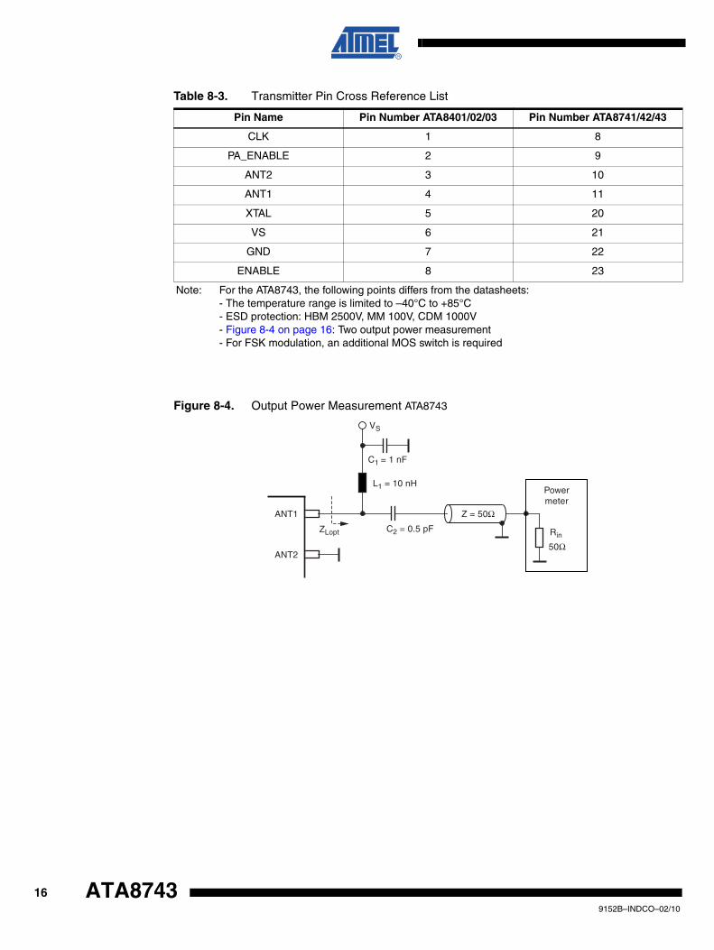
Figure 8-4. Output Power Measurement ATA8743
Table 8-3. Transmitter Pin Cross Reference List
Pin Name Pin Number ATA8401/02/03 Pin Number ATA8741/42/43
CLK 1 8
PA_ENABLE 2 9
ANT2 3 10
ANT1 4 11
XTAL 5 20
VS 6 21
GND 7 22
ENABLE 8 23
Note: For the ATA8743, the following points differs from the datasheets:- The temperature range is limited to –40°C to +85°C- ESD protection: HBM 2500V, MM 100V, CDM 1000V- Figure 8-4 on page 16: Two output power measurement- For FSK modulation, an additional MOS switch is required
L1 = 10 nH
C2 = 0.5 pF
C1 = 1 nF
VS
Rin
ANT2
ANT1
ZLopt
Powermeter
50Ω
Z = 50Ω
169152B–INDCO–02/10
ATA8743
ATA8743
Table 8-4. Microcontroller Cross Reference List
Pin NamePin Number ATtiny44V
Pin Number ATA8741/ATA8742/ATA8743
VCC 1 1
PB0 2 2
PB1 3 3
PB3/NRESET 4 4
PB2 5 5
PA7 6 6
PA6/MOSI 7 7
PA5/MISO 8 13
PA4/USCK 9 14
PA3/T0 10 15
PA2 11 16
PA1 12 17
PA0 13 18
GND 14 19
Note: For the ATA8741/ATA8742/ATA8743, the following points differs from the ATtiny44V data sheet:- The temperature range is limited to –40°C to +85°C- The supply voltage range is limited from 2.0V to 4.0V
179152B–INDCO–02/10

Appendix: Microcontroller ATtiny24/44/84
189152B–INDCO–02/10
ATA8743
ATA8743
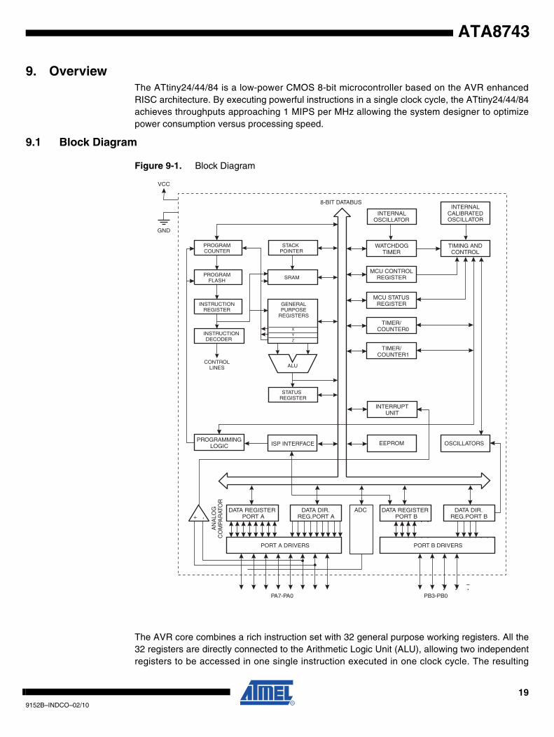
9. OverviewThe ATtiny24/44/84 is a low-power CMOS 8-bit microcontroller based on the AVR enhancedRISC architecture. By executing powerful instructions in a single clock cycle, the ATtiny24/44/84achieves throughputs approaching 1 MIPS per MHz allowing the system designer to optimizepower consumption versus processing speed.
9.1 Block Diagram
Figure 9-1. Block Diagram
The AVR core combines a rich instruction set with 32 general purpose working registers. All the32 registers are directly connected to the Arithmetic Logic Unit (ALU), allowing two independentregisters to be accessed in one single instruction executed in one clock cycle. The resulting
WATCHDOGTIMER
MCU CONTROLREGISTER
TIMER/COUNTER0
DATA DIR.REG.PORT A
DATA REGISTERPORT A
PROGRAMMINGLOGIC
TIMING ANDCONTROL
MCU STATUSREGISTER
PORT A DRIVERS
PA7-PA0
VCC
GND
+ -
AN
ALO
GC
OM
PAR
ATO
R
8-BIT DATABUS
ADC
ISP INTERFACE
INTERRUPTUNIT
EEPROM
INTERNALOSCILLATOR
OSCILLATORS
CALIBRATEDOSCILLATOR
INTERNAL
DATA DIR.REG.PORT B
DATA REGISTERPORT B
PORT B DRIVERS
PB3-PB0
PROGRAMCOUNTER
STACKPOINTER
PROGRAMFLASH SRAM
GENERALPURPOSE
REGISTERS
INSTRUCTIONREGISTER
INSTRUCTIONDECODER
STATUSREGISTER
Z
YX
ALUCONTROL
LINES
TIMER/COUNTER1
199152B–INDCO–02/10
architecture is more code efficient while achieving throughputs up to ten times faster than con-ventional CISC microcontrollers.
The ATtiny24/44/84 provides the following features: 2/4/8K byte of In-System ProgrammableFlash, 128/256/512 bytes EEPROM, 128/256/512 bytes SRAM, 12 general purpose I/O lines, 32general purpose working registers, a 8-bit Timer/Counter with two PWM channels, a 16-bittimer/counter with two PWM channels, Internal and External Interrupts, a 8-channel 10-bit ADC,programmable gain stage (1x, 20x) for 12 differential ADC channel pairs, a programmableWatchdog Timer with internal Oscillator, internal calibrated oscillator, and three software select-able power saving modes. The Idle mode stops the CPU while allowing the SRAM,Timer/Counter, ADC, Analog Comparator, and Interrupt system to continue functioning. ThePower-down mode saves the register contents, disabling all chip functions until the next Inter-rupt or Hardware Reset. The ADC Noise Reduction mode stops the CPU and all I/O modulesexcept ADC, to minimize switching noise during ADC conversions. In Standby mode, the crys-tal/resonator Oscillator is running while the rest of the device is sleeping. This allows very faststart-up combined with low power consumption.
The device is manufactured using Atmel’s high density non-volatile memory technology. TheOn-chip ISP Flash allows the Program memory to be re-programmed In-System through an SPIserial interface, by a conventional non-volatile memory programmer or by an On-chip boot coderunning on the AVR core.
The ATtiny24/44/84 AVR is supported with a full suite of program and system development toolsincluding: C Compilers, Macro Assemblers, Program Debugger/Simulators, In-Circuit Emulators,and Evaluation kits.
9.2 Automotive Quality Grade
The ATtiny24/44/84 have been developed and manufactured according to the most stringentrequirements of the international standard ISO-TS-16949 grade 1. This data sheet contains limitvalues extracted from the results of extensive characterization (Temperature and Voltage). Thequality and reliability of the ATtiny24/44/84 have been verified during regular product qualifica-tion as per AEC-Q100.
As indicated in the ordering information paragraph, the product is available in only one tempera-ture grade,
Table 9-1. Temperature Grade Identification for Automotive Products
Temperature TemperatureIdentifier
Comments
-40; +125 Z Full Automotive Temperature Range
209152B–INDCO–02/10
ATA8743
ATA8743
9.3 Pin Descriptions
9.3.1 VCC
Supply voltage.
9.3.2 GND
Ground.
9.3.3 Port B (PB3...PB0)
Port B is a 4-bit bi-directional I/O port with internal pull-up resistors (selected for each bit). ThePort B output buffers have symmetrical drive characteristics with both high sink and sourcecapability except PB3 which has the RESET capability. To use pin PB3 as an I/O pin, instead ofRESET pin, program (‘0’) RSTDISBL fuse. As inputs, Port B pins that are externally pulled lowwill source current if the pull-up resistors are activated. The Port B pins are tri-stated when areset condition becomes active, even if the clock is not running.
Port B also serves the functions of various special features of the ATtiny24/44/84 as listed onSection 19.3 “Alternate Port Functions” on page 77.
9.3.4 RESET
Reset input. A low level on this pin for longer than the minimum pulse length will generate areset, even if the clock is not running. The minimum pulse length is given in Figure 16-1 on page56. Shorter pulses are not guaranteed to generate a reset.
9.3.5 Port A (PA7...PA0)
Port A is a 8-bit bi-directional I/O port with internal pull-up resistors (selected for each bit). ThePort A output buffers have symmetrical drive characteristics with both high sink and sourcecapability. As inputs, Port A pins that are externally pulled low will source current if the pull-upresistors are activated. The Port A pins are tri-stated when a reset condition becomes active,even if the clock is not running.
Port A has an alternate functions as analog inputs for the ADC, analog comparator, timer/coun-ter, SPI and pin change interrupt as described in “Alternate Port Functions” on page 77
219152B–INDCO–02/10
10. Resources
A comprehensive set of development tools, drivers and application notes, and datasheets areavailable for download on http://www.atmel.com/avr.
11. About Code Examples
This documentation contains simple code examples that briefly show how to use various parts ofthe device. These code examples assume that the part specific header file is included beforecompilation. Be aware that not all C compiler vendors include bit definitions in the header filesand interrupt handling in C is compiler dependent. Please confirm with the C compiler documen-tation for more details.
For I/O Registers located in extended I/O map, “IN”, “OUT”, “SBIS”, “SBIC”, “CBI”, and “SBI”instructions must be replaced with instructions that allow access to extended I/O. Typically“LDS” and “STS” combined with “SBRS”, “SBRC”, “SBR”, and “CBR”.
229152B–INDCO–02/10
ATA8743
ATA8743
12. CPU Core
12.1 Overview
This section discusses the AVR core architecture in general. The main function of the CPU coreis to ensure correct program execution. The CPU must therefore be able to access memories,perform calculations, control peripherals, and handle interrupts.
12.2 Architectural Overview
Figure 12-1. Block Diagram of the AVR Architecture
In order to maximize performance and parallelism, the AVR uses a Harvard architecture – withseparate memories and buses for program and data. Instructions in the Program memory areexecuted with a single level pipelining. While one instruction is being executed, the next instruc-tion is pre-fetched from the Program memory. This concept enables instructions to be executedin every clock cycle. The Program memory is In-System Reprogrammable Flash memory.
FlashProgramMemory
InstructionRegister
InstructionDecoder
ProgramCounter
Control Lines
32 x 8GeneralPurpose
Registrers
ALU
Statusand Control
I/O Lines
EEPROM
Data Bus 8-bit
DataSRAM
Dire
ct A
ddre
ssin
g
Indi
rect
Add
ress
ing
InterruptUnit
WatchdogTimer
AnalogComparator
Timer/Counter 0
Timer/Counter 1
Universal Serial Interface
239152B–INDCO–02/10
The fast-access Register File contains 32 x 8-bit general purpose working registers with a singleclock cycle access time. This allows single-cycle Arithmetic Logic Unit (ALU) operation. In a typ-ical ALU operation, two operands are output from the Register File, the operation is executed,and the result is stored back in the Register File – in one clock cycle.
Six of the 32 registers can be used as three 16-bit indirect address register pointers for DataSpace addressing – enabling efficient address calculations. One of the these address pointerscan also be used as an address pointer for look up tables in Flash Program memory. Theseadded function registers are the 16-bit X-, Y-, and Z-register, described later in this section.
The ALU supports arithmetic and logic operations between registers or between a constant anda register. Single register operations can also be executed in the ALU. After an arithmetic opera-tion, the Status Register is updated to reflect information about the result of the operation.
Program flow is provided by conditional and unconditional jump and call instructions, able todirectly address the whole address space. Most AVR instructions have a single 16-bit word for-mat. Every Program memory address contains a 16- or 32-bit instruction.
During interrupts and subroutine calls, the return address Program Counter (PC) is stored on theStack. The Stack is effectively allocated in the general data SRAM, and consequently the Stacksize is only limited by the total SRAM size and the usage of the SRAM. All user programs mustinitialize the SP in the Reset routine (before subroutines or interrupts are executed). The StackPointer (SP) is read/write accessible in the I/O space. The data SRAM can easily be accessedthrough the five different addressing modes supported in the AVR architecture.
The memory spaces in the AVR architecture are all linear and regular memory maps.
A flexible interrupt module has its control registers in the I/O space with an additional GlobalInterrupt Enable bit in the Status Register. All interrupts have a separate Interrupt Vector in theInterrupt Vector table. The interrupts have priority in accordance with their Interrupt Vector posi-tion. The lower the Interrupt Vector address, the higher the priority.
The I/O memory space contains 64 addresses for CPU peripheral functions as Control Regis-ters, SPI, and other I/O functions. The I/O memory can be accessed directly, or as the DataSpace locations following those of the Register File, 0x20 - 0x5F.
12.3 ALU – Arithmetic Logic Unit
The high-performance AVR ALU operates in direct connection with all the 32 general purposeworking registers. Within a single clock cycle, arithmetic operations between general purposeregisters or between a register and an immediate are executed. The ALU operations are dividedinto three main categories – arithmetic, logical, and bit-functions. Some implementations of thearchitecture also provide a powerful multiplier supporting both signed/unsigned multiplicationand fractional format. See the “Instruction Set” section for a detailed description.
12.4 Status Register
The Status Register contains information about the result of the most recently executed arithme-tic instruction. This information can be used for altering program flow in order to performconditional operations. Note that the Status Register is updated after all ALU operations, asspecified in the Instruction Set Reference. This will in many cases remove the need for using thededicated compare instructions, resulting in faster and more compact code.
The Status Register is not automatically stored when entering an interrupt routine and restoredwhen returning from an interrupt. This must be handled by software.
249152B–INDCO–02/10
ATA8743
ATA8743
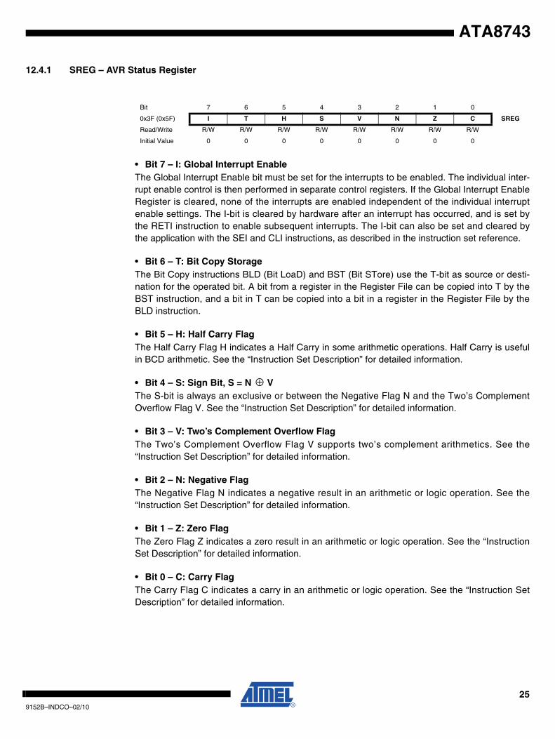
12.4.1 SREG – AVR Status Register
• Bit 7 – I: Global Interrupt EnableThe Global Interrupt Enable bit must be set for the interrupts to be enabled. The individual inter-rupt enable control is then performed in separate control registers. If the Global Interrupt EnableRegister is cleared, none of the interrupts are enabled independent of the individual interruptenable settings. The I-bit is cleared by hardware after an interrupt has occurred, and is set bythe RETI instruction to enable subsequent interrupts. The I-bit can also be set and cleared bythe application with the SEI and CLI instructions, as described in the instruction set reference.
• Bit 6 – T: Bit Copy StorageThe Bit Copy instructions BLD (Bit LoaD) and BST (Bit STore) use the T-bit as source or desti-nation for the operated bit. A bit from a register in the Register File can be copied into T by theBST instruction, and a bit in T can be copied into a bit in a register in the Register File by theBLD instruction.
• Bit 5 – H: Half Carry Flag The Half Carry Flag H indicates a Half Carry in some arithmetic operations. Half Carry is usefulin BCD arithmetic. See the “Instruction Set Description” for detailed information.
• Bit 4 – S: Sign Bit, S = N ⊕ VThe S-bit is always an exclusive or between the Negative Flag N and the Two’s ComplementOverflow Flag V. See the “Instruction Set Description” for detailed information.
• Bit 3 – V: Two’s Complement Overflow FlagThe Two’s Complement Overflow Flag V supports two’s complement arithmetics. See the“Instruction Set Description” for detailed information.
• Bit 2 – N: Negative FlagThe Negative Flag N indicates a negative result in an arithmetic or logic operation. See the“Instruction Set Description” for detailed information.
• Bit 1 – Z: Zero FlagThe Zero Flag Z indicates a zero result in an arithmetic or logic operation. See the “InstructionSet Description” for detailed information.
• Bit 0 – C: Carry FlagThe Carry Flag C indicates a carry in an arithmetic or logic operation. See the “Instruction SetDescription” for detailed information.
Bit 7 6 5 4 3 2 1 0
0x3F (0x5F) I T H S V N Z C SREG
Read/Write R/W R/W R/W R/W R/W R/W R/W R/W
Initial Value 0 0 0 0 0 0 0 0
259152B–INDCO–02/10
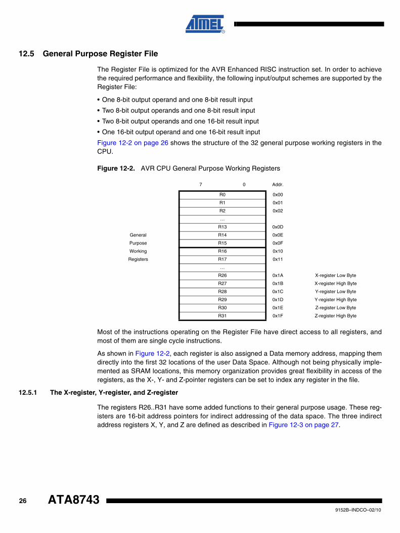
12.5 General Purpose Register File
The Register File is optimized for the AVR Enhanced RISC instruction set. In order to achievethe required performance and flexibility, the following input/output schemes are supported by theRegister File:
• One 8-bit output operand and one 8-bit result input
• Two 8-bit output operands and one 8-bit result input
• Two 8-bit output operands and one 16-bit result input
• One 16-bit output operand and one 16-bit result input
Figure 12-2 on page 26 shows the structure of the 32 general purpose working registers in theCPU.
Figure 12-2. AVR CPU General Purpose Working Registers
Most of the instructions operating on the Register File have direct access to all registers, andmost of them are single cycle instructions.
As shown in Figure 12-2, each register is also assigned a Data memory address, mapping themdirectly into the first 32 locations of the user Data Space. Although not being physically imple-mented as SRAM locations, this memory organization provides great flexibility in access of theregisters, as the X-, Y- and Z-pointer registers can be set to index any register in the file.
12.5.1 The X-register, Y-register, and Z-register
The registers R26..R31 have some added functions to their general purpose usage. These reg-isters are 16-bit address pointers for indirect addressing of the data space. The three indirectaddress registers X, Y, and Z are defined as described in Figure 12-3 on page 27.
7 0 Addr.
R0 0x00
R1 0x01
R2 0x02
…
R13 0x0D
General R14 0x0E
Purpose R15 0x0F
Working R16 0x10
Registers R17 0x11
…
R26 0x1A X-register Low Byte
R27 0x1B X-register High Byte
R28 0x1C Y-register Low Byte
R29 0x1D Y-register High Byte
R30 0x1E Z-register Low Byte
R31 0x1F Z-register High Byte
269152B–INDCO–02/10
ATA8743
ATA8743
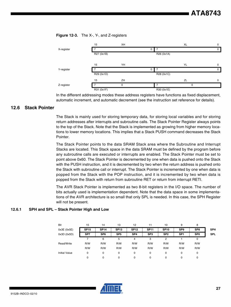
Figure 12-3. The X-, Y-, and Z-registers
In the different addressing modes these address registers have functions as fixed displacement,automatic increment, and automatic decrement (see the instruction set reference for details).
12.6 Stack Pointer
The Stack is mainly used for storing temporary data, for storing local variables and for storingreturn addresses after interrupts and subroutine calls. The Stack Pointer Register always pointsto the top of the Stack. Note that the Stack is implemented as growing from higher memory loca-tions to lower memory locations. This implies that a Stack PUSH command decreases the StackPointer.
The Stack Pointer points to the data SRAM Stack area where the Subroutine and InterruptStacks are located. This Stack space in the data SRAM must be defined by the program beforeany subroutine calls are executed or interrupts are enabled. The Stack Pointer must be set topoint above 0x60. The Stack Pointer is decremented by one when data is pushed onto the Stackwith the PUSH instruction, and it is decremented by two when the return address is pushed ontothe Stack with subroutine call or interrupt. The Stack Pointer is incremented by one when data ispopped from the Stack with the POP instruction, and it is incremented by two when data ispopped from the Stack with return from subroutine RET or return from interrupt RETI.
The AVR Stack Pointer is implemented as two 8-bit registers in the I/O space. The number ofbits actually used is implementation dependent. Note that the data space in some implementa-tions of the AVR architecture is so small that only SPL is needed. In this case, the SPH Registerwill not be present.
12.6.1 SPH and SPL – Stack Pointer High and Low
15 XH XL 0
X-register 7 0 7 0
R27 (0x1B) R26 (0x1A)
15 YH YL 0
Y-register 7 0 7 0
R29 (0x1D) R28 (0x1C)
15 ZH ZL 0
Z-register 7 0 7 0
R31 (0x1F) R30 (0x1E)
Bit 15 14 13 12 11 10 9 8
0x3E (0x5E) SP15 SP14 SP13 SP12 SP11 SP10 SP9 SP8 SPH
0x3D (0x5D) SP7 SP6 SP5 SP4 SP3 SP2 SP1 SP0 SPL
7 6 5 4 3 2 1 0
Read/Write R/W R/W R/W R/W R/W R/W R/W R/W
R/W R/W R/W R/W R/W R/W R/W R/W
Initial Value 0 0 0 0 0 0 0 0
0 0 0 0 0 0 0 0
279152B–INDCO–02/10
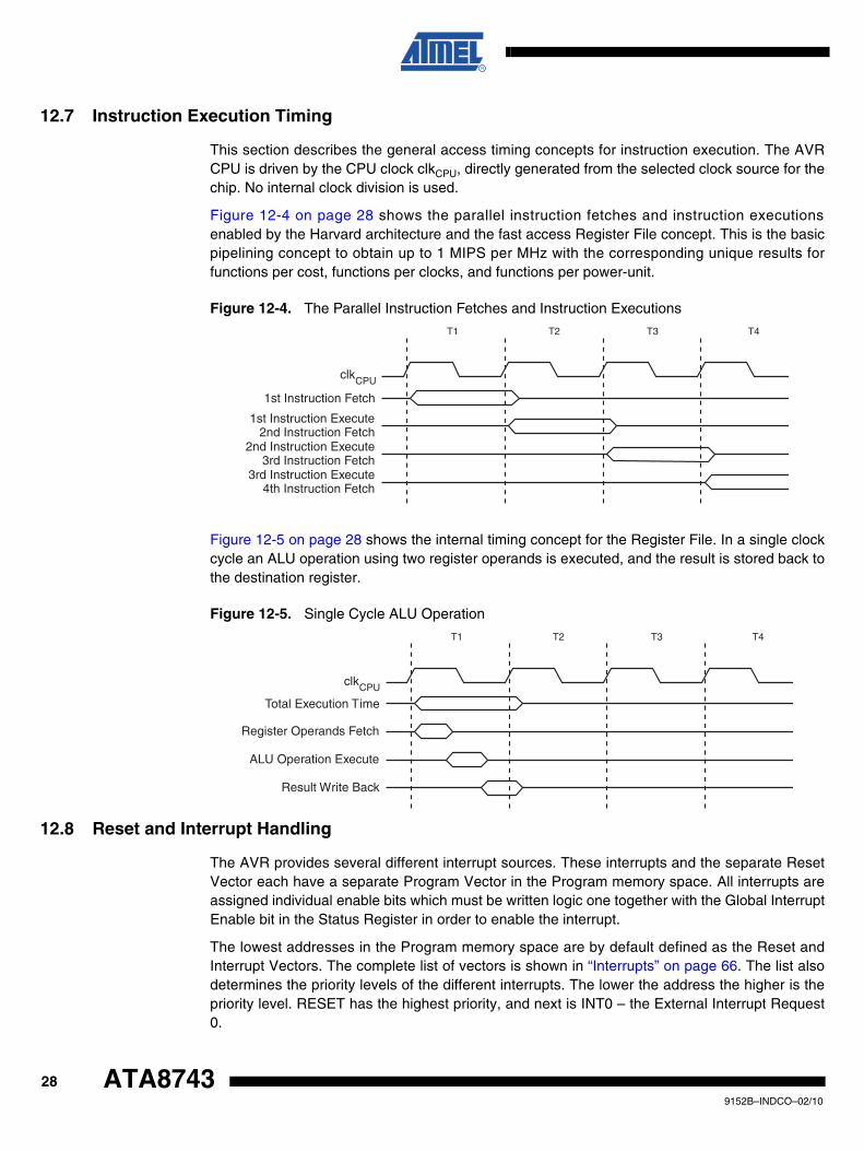
12.7 Instruction Execution Timing
This section describes the general access timing concepts for instruction execution. The AVRCPU is driven by the CPU clock clkCPU, directly generated from the selected clock source for thechip. No internal clock division is used.
Figure 12-4 on page 28 shows the parallel instruction fetches and instruction executionsenabled by the Harvard architecture and the fast access Register File concept. This is the basicpipelining concept to obtain up to 1 MIPS per MHz with the corresponding unique results forfunctions per cost, functions per clocks, and functions per power-unit.
Figure 12-4. The Parallel Instruction Fetches and Instruction Executions
Figure 12-5 on page 28 shows the internal timing concept for the Register File. In a single clockcycle an ALU operation using two register operands is executed, and the result is stored back tothe destination register.
Figure 12-5. Single Cycle ALU Operation
12.8 Reset and Interrupt Handling
The AVR provides several different interrupt sources. These interrupts and the separate ResetVector each have a separate Program Vector in the Program memory space. All interrupts areassigned individual enable bits which must be written logic one together with the Global InterruptEnable bit in the Status Register in order to enable the interrupt.
The lowest addresses in the Program memory space are by default defined as the Reset andInterrupt Vectors. The complete list of vectors is shown in “Interrupts” on page 66. The list alsodetermines the priority levels of the different interrupts. The lower the address the higher is thepriority level. RESET has the highest priority, and next is INT0 – the External Interrupt Request0.
clk
1st Instruction Fetch
1st Instruction Execute2nd Instruction Fetch
2nd Instruction Execute3rd Instruction Fetch
3rd Instruction Execute4th Instruction Fetch
T1 T2 T3 T4
CPU
Total Execution Time
Register Operands Fetch
ALU Operation Execute
Result Write Back
T1 T2 T3 T4
clkCPU
289152B–INDCO–02/10
ATA8743
ATA8743
When an interrupt occurs, the Global Interrupt Enable I-bit is cleared and all interrupts are dis-abled. The user software can write logic one to the I-bit to enable nested interrupts. All enabledinterrupts can then interrupt the current interrupt routine. The I-bit is automatically set when aReturn from Interrupt instruction – RETI – is executed.
There are basically two types of interrupts. The first type is triggered by an event that sets theInterrupt Flag. For these interrupts, the Program Counter is vectored to the actual Interrupt Vec-tor in order to execute the interrupt handling routine, and hardware clears the correspondingInterrupt Flag. Interrupt Flags can also be cleared by writing a logic one to the flag bit position(s)to be cleared. If an interrupt condition occurs while the corresponding interrupt enable bit iscleared, the Interrupt Flag will be set and remembered until the interrupt is enabled, or the flag iscleared by software. Similarly, if one or more interrupt conditions occur while the Global InterruptEnable bit is cleared, the corresponding Interrupt Flag(s) will be set and remembered until theGlobal Interrupt Enable bit is set, and will then be executed by order of priority.
The second type of interrupts will trigger as long as the interrupt condition is present. Theseinterrupts do not necessarily have Interrupt Flags. If the interrupt condition disappears before theinterrupt is enabled, the interrupt will not be triggered.
When the AVR exits from an interrupt, it will always return to the main program and execute onemore instruction before any pending interrupt is served.
Note that the Status Register is not automatically stored when entering an interrupt routine, norrestored when returning from an interrupt routine. This must be handled by software.
When using the CLI instruction to disable interrupts, the interrupts will be immediately disabled.No interrupt will be executed after the CLI instruction, even if it occurs simultaneously with theCLI instruction. The following example shows how this can be used to avoid interrupts during thetimed EEPROM write sequence..
Assembly Code Example
in r16, SREG ; store SREG value
cli ; disable interrupts during timed sequence
sbi EECR, EEMPE ; start EEPROM write
sbi EECR, EEPE
out SREG, r16 ; restore SREG value (I-bit)
C Code Example
char cSREG;
cSREG = SREG; /* store SREG value */
/* disable interrupts during timed sequence */
_CLI();
EECR |= (1<<EEMPE); /* start EEPROM write */
EECR |= (1<<EEPE);
SREG = cSREG; /* restore SREG value (I-bit) */
299152B–INDCO–02/10
When using the SEI instruction to enable interrupts, the instruction following SEI will be exe-cuted before any pending interrupts, as shown in this example.
12.8.1 Interrupt Response Time
The interrupt execution response for all the enabled AVR interrupts is four clock cycles mini-mum. After four clock cycles the Program Vector address for the actual interrupt handling routineis executed. During this four clock cycle period, the Program Counter is pushed onto the Stack.The vector is normally a jump to the interrupt routine, and this jump takes three clock cycles. Ifan interrupt occurs during execution of a multi-cycle instruction, this instruction is completedbefore the interrupt is served. If an interrupt occurs when the MCU is in sleep mode, the interruptexecution response time is increased by four clock cycles. This increase comes in addition to thestart-up time from the selected sleep mode.
A return from an interrupt handling routine takes four clock cycles. During these four clockcycles, the Program Counter (two bytes) is popped back from the Stack, the Stack Pointer isincremented by two, and the I-bit in SREG is set.
Assembly Code Example
sei ; set Global Interrupt Enable
sleep; enter sleep, waiting for interrupt
; note: will enter sleep before any pending
; interrupt(s)
C Code Example
_SEI(); /* set Global Interrupt Enable */
_SLEEP(); /* enter sleep, waiting for interrupt */
/* note: will enter sleep before any pending interrupt(s) */
309152B–INDCO–02/10
ATA8743
ATA8743
13. Memories
This section describes the different memories in the ATtiny24/44/84. The AVR architecture hastwo main memory spaces, the Data memory and the Program memory space. In addition, theATtiny24/44/84 features an EEPROM Memory for data storage. All three memory spaces are lin-ear and regular.
13.1 In-System Re-programmable Flash Program Memory
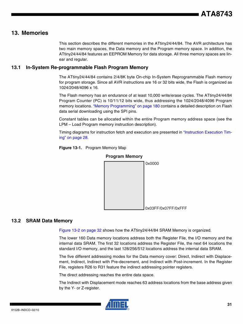
The ATtiny24/44/84 contains 2/4/8K byte On-chip In-System Reprogrammable Flash memoryfor program storage. Since all AVR instructions are 16 or 32 bits wide, the Flash is organized as1024/2048/4096 x 16.
The Flash memory has an endurance of at least 10,000 write/erase cycles. The ATtiny24/44/84Program Counter (PC) is 10/11/12 bits wide, thus addressing the 1024/2048/4096 Programmemory locations. “Memory Programming” on page 180 contains a detailed description on Flashdata serial downloading using the SPI pins.
Constant tables can be allocated within the entire Program memory address space (see theLPM – Load Program memory instruction description).
Timing diagrams for instruction fetch and execution are presented in “Instruction Execution Tim-ing” on page 28.
Figure 13-1. Program Memory Map
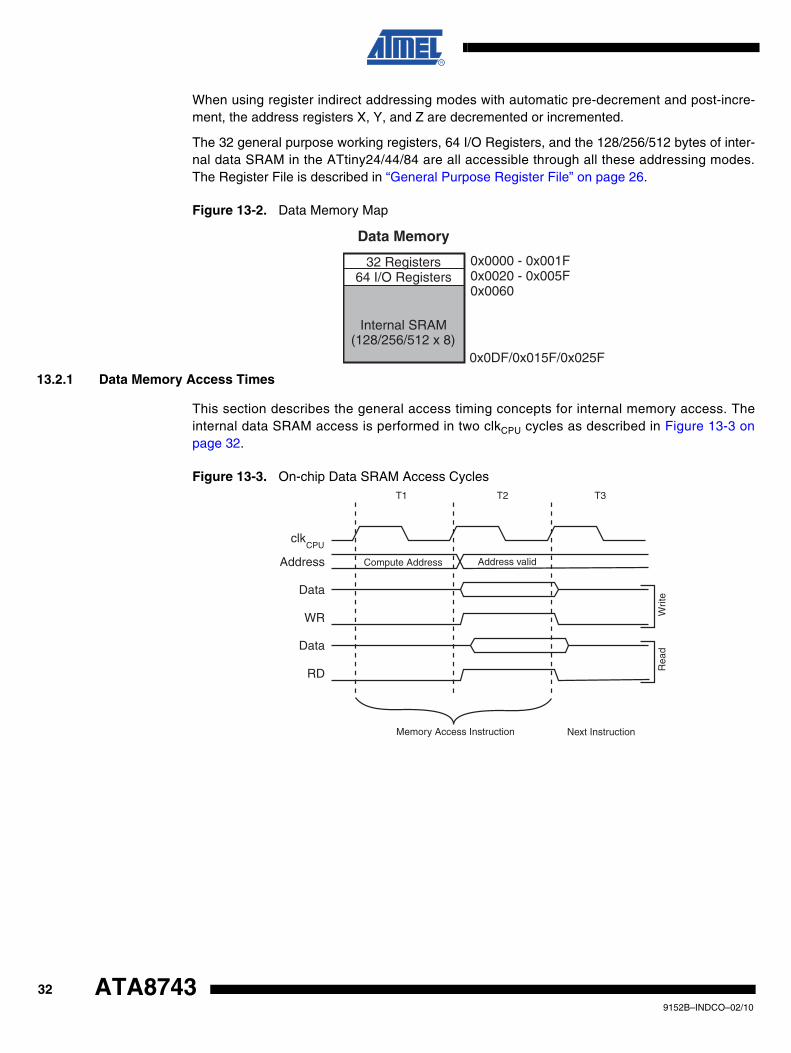
13.2 SRAM Data Memory
Figure 13-2 on page 32 shows how the ATtiny24/44/84 SRAM Memory is organized.
The lower 160 Data memory locations address both the Register File, the I/O memory and theinternal data SRAM. The first 32 locations address the Register File, the next 64 locations thestandard I/O memory, and the last 128/256/512 locations address the internal data SRAM.
The five different addressing modes for the Data memory cover: Direct, Indirect with Displace-ment, Indirect, Indirect with Pre-decrement, and Indirect with Post-increment. In the RegisterFile, registers R26 to R31 feature the indirect addressing pointer registers.
The direct addressing reaches the entire data space.
The Indirect with Displacement mode reaches 63 address locations from the base address givenby the Y- or Z-register.
0x0000
0x03FF/0x07FF/0xFFF
Program Memory
319152B–INDCO–02/10
When using register indirect addressing modes with automatic pre-decrement and post-incre-ment, the address registers X, Y, and Z are decremented or incremented.
The 32 general purpose working registers, 64 I/O Registers, and the 128/256/512 bytes of inter-nal data SRAM in the ATtiny24/44/84 are all accessible through all these addressing modes.The Register File is described in “General Purpose Register File” on page 26.
Figure 13-2. Data Memory Map
13.2.1 Data Memory Access Times
This section describes the general access timing concepts for internal memory access. Theinternal data SRAM access is performed in two clkCPU cycles as described in Figure 13-3 onpage 32.
Figure 13-3. On-chip Data SRAM Access Cycles
32 Registers64 I/O Registers
Internal SRAM(128/256/512 x 8)
0x0000 - 0x001F0x0020 - 0x005F
0x0DF/0x015F/0x025F
0x0060
Data Memory
clk
WR
RD
Data
Data
Address Address valid
T1 T2 T3
Compute Address
Rea
dW
rite
CPU
Memory Access Instruction Next Instruction
329152B–INDCO–02/10
ATA8743
ATA8743
13.3 EEPROM Data Memory
The ATtiny24/44/84 contains 128/256/512 bytes of data EEPROM memory. It is organized as aseparate data space, in which single bytes can be read and written. The EEPROM has anendurance of at least 100,000 write/erase cycles. The access between the EEPROM and theCPU is described in the following, specifying the EEPROM Address Registers, the EEPROMData Register, and the EEPROM Control Register. For a detailed description of Serial datadownloading to the EEPROM, see “Serial Downloading” on page 184.
13.3.1 EEPROM Read/Write Access
The EEPROM Access Registers are accessible in the I/O space.
The write access times for the EEPROM are given in Table 13-1 on page 39. A self-timing func-tion, however, lets the user software detect when the next byte can be written. If the user codecontains instructions that write the EEPROM, some precautions must be taken. In heavily fil-tered power supplies, VCC is likely to rise or fall slowly on Power-up/down. This causes thedevice for some period of time to run at a voltage lower than specified as minimum for the clockfrequency used. See “Preventing EEPROM Corruption” on page 36 for details on how to avoidproblems in these situations.
In order to prevent unintentional EEPROM writes, a specific write procedure must be followed.See “Atomic Byte Programming” on page 33 and “Split Byte Programming” on page 33 fordetails on this.
When the EEPROM is read, the CPU is halted for four clock cycles before the next instruction isexecuted. When the EEPROM is written, the CPU is halted for two clock cycles before the nextinstruction is executed.
13.3.2 Atomic Byte Programming
Using Atomic Byte Programming is the simplest mode. When writing a byte to the EEPROM, theuser must write the address into the EEARL Register and data into EEDR Register. If theEEPMn bits are zero, writing EEPE (within four cycles after EEMPE is written) will trigger theerase/write operation. Both the erase and write cycle are done in one operation and the totalprogramming time is given in Table 1. The EEPE bit remains set until the erase and write opera-tions are completed. While the device is busy with programming, it is not possible to do anyother EEPROM operations.
13.3.3 Split Byte Programming
It is possible to split the erase and write cycle in two different operations. This may be useful ifthe system requires short access time for some limited period of time (typically if the power sup-ply voltage falls). In order to take advantage of this method, it is required that the locations to bewritten have been erased before the write operation. But since the erase and write operationsare split, it is possible to do the erase operations when the system allows doing time-criticaloperations (typically after Power-up).
13.3.4 Erase
To erase a byte, the address must be written to EEAR. If the EEPMn bits are 0b01, writing theEEPE (within four cycles after EEMPE is written) will trigger the erase operation only (program-ming time is given in Table 1). The EEPE bit remains set until the erase operation completes.While the device is busy programming, it is not possible to do any other EEPROM operations.
339152B–INDCO–02/10
13.3.5 Write
To write a location, the user must write the address into EEAR and the data into EEDR. If theEEPMn bits are 0b10, writing the EEPE (within four cycles after EEMPE is written) will triggerthe write operation only (programming time is given in Table 1). The EEPE bit remains set untilthe write operation completes. If the location to be written has not been erased before write, thedata that is stored must be considered as lost. While the device is busy with programming, it isnot possible to do any other EEPROM operations.
The calibrated Oscillator is used to time the EEPROM accesses. Make sure the Oscillator fre-quency is within the requirements described in “Oscillator Calibration Register – OSCCAL” onpage 48.
The following code examples show one assembly and one C function for erase, write, or atomicwrite of the EEPROM. The examples assume that interrupts are controlled (e.g., by disablinginterrupts globally) so that no interrupts will occur during execution of these functions.
349152B–INDCO–02/10
ATA8743
ATA8743
Note: The code examples are only valid for ATtiny24 and ATtiny44, using 8-bit addressing mode.
Assembly Code Example
EEPROM_write:
; Wait for completion of previous write
sbic EECR,EEPE
rjmp EEPROM_write
; Set Programming mode
ldi r16, (0<<EEPM1)|(0<<EEPM0)
out EECR, r16
; Set up address (r17) in address register
out EEARL, r17
; Write data (r16) to data register
out EEDR,r16
; Write logical one to EEMPE
sbi EECR,EEMPE
; Start eeprom write by setting EEPE
sbi EECR,EEPE
ret
C Code Example
void EEPROM_write(unsigned char ucAddress, unsigned char ucData)
{
/* Wait for completion of previous write */
while(EECR & (1<<EEPE))
;
/* Set Programming mode */
EECR = (0<<EEPM1)|(0>>EEPM0)
/* Set up address and data registers */
EEARL = ucAddress;
EEDR = ucData;
/* Write logical one to EEMPE */
EECR |= (1<<EEMPE);
/* Start eeprom write by setting EEPE */
EECR |= (1<<EEPE);
}
359152B–INDCO–02/10
The next code examples show assembly and C functions for reading the EEPROM. The exam-ples assume that interrupts are controlled so that no interrupts will occur during execution ofthese functions.
Note: The code examples are only valid for ATtiny24 and ATtiny44, using 8-bit addressing mode.
13.3.6 Preventing EEPROM Corruption
During periods of low VCC, the EEPROM data can be corrupted because the supply voltage istoo low for the CPU and the EEPROM to operate properly. These issues are the same as forboard level systems using EEPROM, and the same design solutions should be applied.
An EEPROM data corruption can be caused by two situations when the voltage is too low. First,a regular write sequence to the EEPROM requires a minimum voltage to operate correctly. Sec-ondly, the CPU itself can execute instructions incorrectly, if the supply voltage is too low.
EEPROM data corruption can easily be avoided by following this design recommendation:
Keep the AVR RESET active (low) during periods of insufficient power supply voltage. This canbe done by enabling the internal Brown-out Detector (BOD). If the detection level of the internalBOD does not match the needed detection level, an external low VCC reset protection circuit canbe used. If a reset occurs while a write operation is in progress, the write operation will be com-pleted provided that the power supply voltage is sufficient.
Assembly Code Example
EEPROM_read:
; Wait for completion of previous write
sbic EECR,EEPE
rjmp EEPROM_read
; Set up address (r17) in address register
out EEARL, r17
; Start eeprom read by writing EERE
sbi EECR,EERE
; Read data from data register
in r16,EEDR
ret
C Code Example
unsigned char EEPROM_read(unsigned char ucAddress)
{
/* Wait for completion of previous write */
while(EECR & (1<<EEPE))
;
/* Set up address register */
EEARL = ucAddress;
/* Start eeprom read by writing EERE */
EECR |= (1<<EERE);
/* Return data from data register */
return EEDR;
}
369152B–INDCO–02/10
ATA8743
ATA8743
13.4 I/O Memory
The I/O space definition of the ATtiny24/44/84 is shown in “Register Summary” on page 228.
All ATtiny24/44/84 I/Os and peripherals are placed in the I/O space. All I/O locations may beaccessed by the LD/LDS/LDD and ST/STS/STD instructions, transferring data between the 32general purpose working registers and the I/O space. I/O Registers within the address range0x00 - 0x1F are directly bit-accessible using the SBI and CBI instructions. In these registers, thevalue of single bits can be checked by using the SBIS and SBIC instructions. See the instructionset section for more details. When using the I/O specific commands IN and OUT, the I/Oaddresses 0x00 - 0x3F must be used. When addressing I/O Registers as data space using LDand ST instructions, 0x20 must be added to these addresses.
For compatibility with future devices, reserved bits should be written to zero if accessed.Reserved I/O memory addresses should never be written.
Some of the Status Flags are cleared by writing a logical one to them. Note that, unlike mostother AVRs, the CBI and SBI instructions will only operate on the specified bit, and can thereforebe used on registers containing such Status Flags. The CBI and SBI instructions work with reg-isters 0x00 to 0x1F only.
The I/O and Peripherals Control Registers are explained in later sections.
13.4.1 General Purpose I/O Registers
The ATtiny24/44/84 contains three General Purpose I/O Registers. These registers can be usedfor storing any information, and they are particularly useful for storing global variables and statusflags. General Purpose I/O Registers within the address range 0x00 - 0x1F are directlybit-accessible using the SBI, CBI, SBIS, and SBIC instructions.
379152B–INDCO–02/10
13.5 Register Description
13.5.1 EEARH – EEPROM Address Register
• Bits 7..1 – Res: Reserved BitsThese bits are reserved bits in the ATtiny24/44/84 and will always read as zero.
• Bit 0 – EEAR8: EEPROM AddressThe EEPROM Address Register – EEARH – specifies the most significant bit for EEPROMaddress in the 512 bytes EEPROM space for Tiny84. This bit is reserved bit in the ATtiny24/44and will always read as zero. The initial value of EEAR is undefined. A proper value must bewritten before the EEPROM may be accessed.
13.5.2 EEARL – EEPROM Address Register
• Bits 7..0 – EEAR7..0: EEPROM AddressThe EEPROM Address Register – EEARL – specifies the EEPROM address. In the 128 bytesEEPROM space in ATiny24 bit 7 is reserved and always read as zero. The EEPROM data bytesare addressed linearly between 0 and 128/256/512. The initial value of EEAR is undefined. Aproper value must be written before the EEPROM may be accessed.
13.5.3 EEDR – EEPROM Data Register
• Bits 7..0 – EEDR7..0: EEPROM DataFor the EEPROM write operation the EEDR Register contains the data to be written to theEEPROM in the address given by the EEAR Register. For the EEPROM read operation, theEEDR contains the data read out from the EEPROM at the address given by EEAR.
13.5.4 EECR – EEPROM Control Register
Bit 7 6 5 4 3 2 1 0
0x1F (0x3F) – – – – – – – EEAR8 EEARH
Read/Write R R R R R R R R/W
Initial Value 0 0 0 0 0 0 0 X
Bit 7 6 5 4 3 2 1 0
0x1E (0x3E) EEAR7 EEAR6 EEAR5 EEAR4 EEAR3 EEAR2 EEAR1 EEAR0 EEARL
Read/Write R/W R/W R/W R/W R/W R/W R/W R/W
Initial Value X X X X X X X X
Bit 7 6 5 4 3 2 1 0
0x1D (0x3D) EEDR7 EEDR6 EEDR5 EEDR4 EEDR3 EEDR2 EEDR1 EEDR0 EEDR
Read/Write R/W R/W R/W R/W R/W R/W R/W R/W
Initial Value 0 0 0 0 0 0 0 0
Bit 7 6 5 4 3 2 1 0
0x1C (0x3C) – – EEPM1 EEPM0 EERIE EEMPE EEPE EERE EECR
Read/Write R R R/W R/W R/W R/W R/W R/W
Initial Value 0 0 X X 0 0 X 0
389152B–INDCO–02/10
ATA8743
ATA8743
• Bit 7 – Res: Reserved BitThis bit is reserved for future use and will always read as 0 in ATtiny24/44/84. For compatibilitywith future AVR devices, always write this bit to zero. After reading, mask out this bit.
• Bit 6 – Res: Reserved BitThis bit is reserved in the ATtiny24/44/84 and will always read as zero.
• Bits 5, 4 – EEPM1 and EEPM0: EEPROM Mode Bits
The EEPROM Programming mode bits setting defines which programming action that will betriggered when writing EEPE. It is possible to program data in one atomic operation (erase theold value and program the new value) or to split the Erase and Write operations in two differentoperations. The Programming times for the different modes are shown in Table 13-1. WhileEEPE is set, any write to EEPMn will be ignored. During reset, the EEPMn bits will be reset to0b00 unless the EEPROM is busy programming.
• Bit 3 – EERIE: EEPROM Ready Interrupt EnableWriting EERIE to one enables the EEPROM Ready Interrupt if the I-bit in SREG is set. WritingEERIE to zero disables the interrupt. The EEPROM Ready Interrupt generates a constant inter-rupt when Non-volatile memory is ready for programming.
• Bit 2 – EEMPE: EEPROM Master Program EnableThe EEMPE bit determines whether writing EEPE to one will have effect or not.
When EEMPE is set, setting EEPE within four clock cycles will program the EEPROM at theselected address. If EEMPE is zero, setting EEPE will have no effect. When EEMPE has beenwritten to one by software, hardware clears the bit to zero after four clock cycles.
• Bit 1 – EEPE: EEPROM Program EnableThe EEPROM Program Enable Signal EEPE is the programming enable signal to the EEPROM.When EEPE is written, the EEPROM will be programmed according to the EEPMn bits setting.The EEMPE bit must be written to one before a logical one is written to EEPE, otherwise noEEPROM write takes place. When the write access time has elapsed, the EEPE bit is cleared byhardware. When EEPE has been set, the CPU is halted for two cycles before the next instructionis executed.
• Bit 0 – EERE: EEPROM Read EnableThe EEPROM Read Enable Signal – EERE – is the read strobe to the EEPROM. When the cor-rect address is set up in the EEAR Register, the EERE bit must be written to one to trigger the
Table 13-1. EEPROM Mode Bits
EEPM1 EEPM0Programming
Time Operation
0 0 3.4 ms Erase and Write in one operation (Atomic Operation)
0 1 1.8 ms Erase Only
1 0 1.8 ms Write Only
1 1 – Reserved for future use
399152B–INDCO–02/10
EEPROM read. The EEPROM read access takes one instruction, and the requested data isavailable immediately. When the EEPROM is read, the CPU is halted for four cycles before thenext instruction is executed. The user should poll the EEPE bit before starting the read opera-tion. If a write operation is in progress, it is neither possible to read the EEPROM, nor to changethe EEAR Register.
13.5.5 GPIOR2 – General Purpose I/O Register 2
13.5.6 GPIOR1 – General Purpose I/O Register 1
13.5.7 GPIOR0 – General Purpose I/O Register 0
Bit 7 6 5 4 3 2 1 0
0x15 (0x35) MSB LSB GPIOR2
Read/Write R/W R/W R/W R/W R/W R/W R/W R/W
Initial Value 0 0 0 0 0 0 0 0
Bit 7 6 5 4 3 2 1 0
0x14 (0x34) MSB LSB GPIOR1
Read/Write R/W R/W R/W R/W R/W R/W R/W R/W
Initial Value 0 0 0 0 0 0 0 0
Bit 7 6 5 4 3 2 1 0
0x13 (0x33) MSB LSB GPIOR0
Read/Write R/W R/W R/W R/W R/W R/W R/W R/W
Initial Value 0 0 0 0 0 0 0 0
409152B–INDCO–02/10
ATA8743
ATA8743
14. System Clock and Clock Options
14.1 Clock Systems and their Distribution
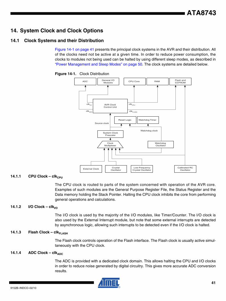
Figure 14-1 on page 41 presents the principal clock systems in the AVR and their distribution. Allof the clocks need not be active at a given time. In order to reduce power consumption, theclocks to modules not being used can be halted by using different sleep modes, as described in“Power Management and Sleep Modes” on page 50. The clock systems are detailed below.
Figure 14-1. Clock Distribution
14.1.1 CPU Clock – clkCPU
The CPU clock is routed to parts of the system concerned with operation of the AVR core.Examples of such modules are the General Purpose Register File, the Status Register and theData memory holding the Stack Pointer. Halting the CPU clock inhibits the core from performinggeneral operations and calculations.
14.1.2 I/O Clock – clkI/O
The I/O clock is used by the majority of the I/O modules, like Timer/Counter. The I/O clock isalso used by the External Interrupt module, but note that some external interrupts are detectedby asynchronous logic, allowing such interrupts to be detected even if the I/O clock is halted.
14.1.3 Flash Clock – clkFLASH
The Flash clock controls operation of the Flash interface. The Flash clock is usually active simul-taneously with the CPU clock.
14.1.4 ADC Clock – clkADC
The ADC is provided with a dedicated clock domain. This allows halting the CPU and I/O clocksin order to reduce noise generated by digital circuitry. This gives more accurate ADC conversionresults.
General I/OModules
CPU Core RAM
clkI/O AVR ClockControl Unit
clkCPU
Flash andEEPROM
clkFLASH
Source clock
Watchdog Timer
WatchdogOscillator
Reset Logic
ClockMultiplexer
Watchdog clock
Calibrated RCOscillator
Calibrated RCOscillator
External Clock
ADC
clkADC
CrystalOscillator
Low-FrequencyCrystal Oscillator
System ClockPrescaler
419152B–INDCO–02/10
14.2 Clock Sources
The device has the following clock source options, selectable by Flash Fuse bits as shownbelow. The clock from the selected source is input to the AVR clock generator, and routed to theappropriate modules.
Note: 1. For all fuses “1” means unprogrammed while “0” means programmed.
The various choices for each clocking option is given in the following sections. When the CPUwakes up from Power-down or Power-save, the selected clock source is used to time thestart-up, ensuring stable Oscillator operation before instruction execution starts. When the CPUstarts from reset, there is an additional delay allowing the power to reach a stable level beforecommencing normal operation. The Watchdog Oscillator is used for timing this real-time part ofthe start-up time. The number of WDT Oscillator cycles used for each time-out is shown in Table14-2 on page 42.
14.3 Default Clock Source
The device is shipped with CKSEL = “0010”, SUT = “10”, and CKDIV8 programmed. The defaultclock source setting is therefore the Internal RC Oscillator running at 8.0 MHz with longeststart-up time and an initial system clock prescaling of 8, resulting in 1.0 MHz system clock. Thisdefault setting ensures that all users can make their desired clock source setting using anIn-System or High-voltage Programmer.
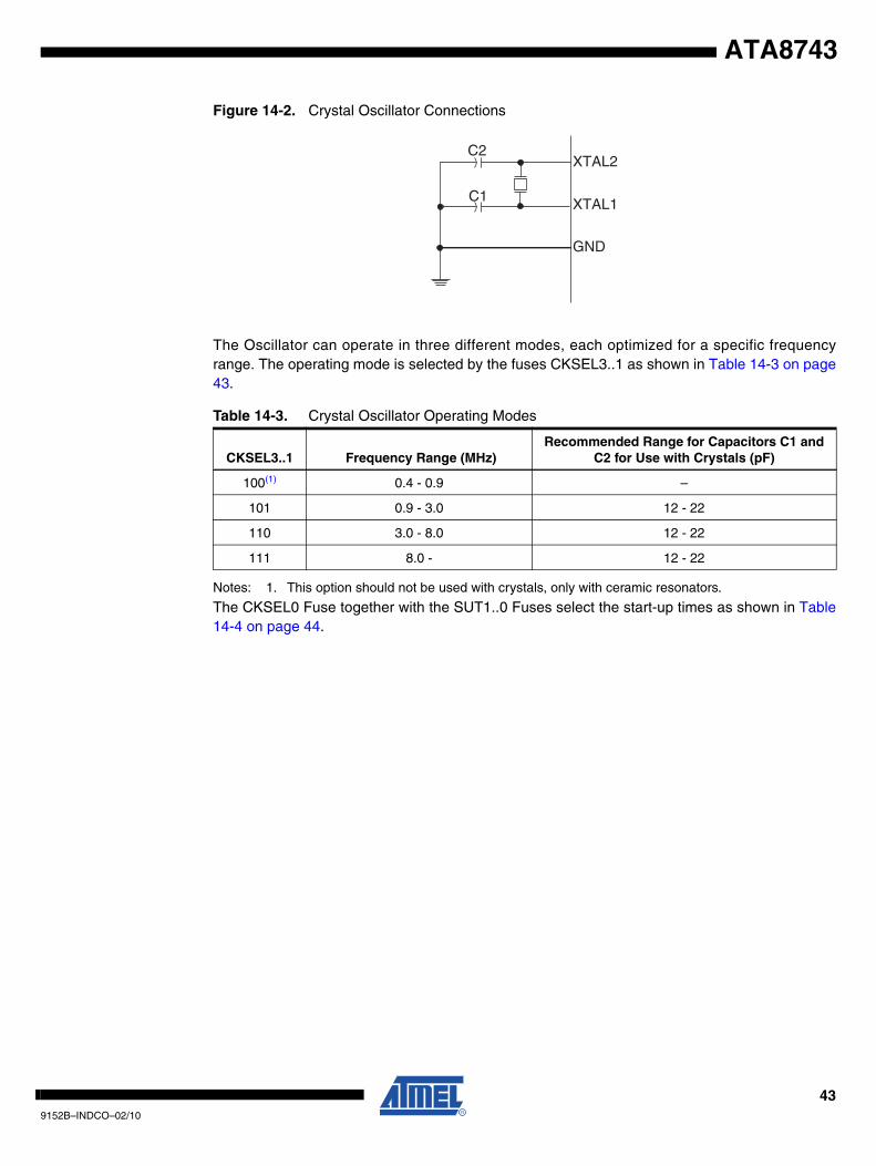
14.4 Crystal Oscillator
XTAL1 and XTAL2 are input and output, respectively, of an inverting amplifier which can
be configured for use as an On-chip Oscillator, as shown in Figure 14-2. Either a quartz
crystal or a ceramic resonator may be used.
C1 and C2 should always be equal for both crystals and resonators. The optimal value of thecapacitors depends on the crystal or resonator in use, the amount of stray capacitance, and theelectromagnetic noise of the environment. Some initial guidelines for choosing capacitors foruse with crystals are given in Table 14-3 on page 43. For ceramic resonators, the capacitor val-ues given by the manufacturer should be used.
Table 14-1. Device Clocking Options Select(1)
Device Clocking Option CKSEL3..0
External Clock 0000
Calibrated Internal RC Oscillator 8.0 MHz 0010
Watchdog Oscillator 128 kHz 0100
External Low-frequency Oscillator 0110
External Crystal/Ceramic Resonator 1000-1111
Reserved 0101, 0111, 0011,0001
Table 14-2. Number of Watchdog Oscillator Cycles
Typ Time-out Number of Cycles
4 ms 512
64 ms 8K (8,192)
429152B–INDCO–02/10
ATA8743
ATA8743
Figure 14-2. Crystal Oscillator Connections
The Oscillator can operate in three different modes, each optimized for a specific frequencyrange. The operating mode is selected by the fuses CKSEL3..1 as shown in Table 14-3 on page43.
Notes: 1. This option should not be used with crystals, only with ceramic resonators.
The CKSEL0 Fuse together with the SUT1..0 Fuses select the start-up times as shown in Table14-4 on page 44.
Table 14-3. Crystal Oscillator Operating Modes
CKSEL3..1 Frequency Range (MHz)Recommended Range for Capacitors C1 and
C2 for Use with Crystals (pF)
100(1) 0.4 - 0.9 –
101 0.9 - 3.0 12 - 22
110 3.0 - 8.0 12 - 22
111 8.0 - 12 - 22
XTAL2
XTAL1
GND
C2
C1
439152B–INDCO–02/10
Notes: 1. These options should only be used when not operating close to the maximum frequency of the device, and only if frequency stability at start-up is not important for the application. These options are not suitable for crystals.
2. These options are intended for use with ceramic resonators and will ensure frequency stability at start-up. They can also be used with crystals when not operating close to the maximum fre-quency of the device, and if frequency stability at start-up is not important for the application.
14.5 Low-frequency Crystal Oscillator
To use a 32.768 kHz watch crystal as the clock source for the device, the low-frequency crystaloscillator must be selected by setting CKSEL fuses to ‘0110’. The crystal should be connectedas shown in Figure 14-2. See the 32 kHz Crystal Oscillator Application Note for details on oscil-lator operation and how to choose appropriate values for C1 and C2.
When this oscillator is selected, start-up times are determined by the SUT fuses as shown inTable 14-5.
Notes: 1. These options should only be used if frequency stability at start-up is not important for the application.
Table 14-4. Start-up Times for the Crystal Oscillator Clock Selection
CKSEL0 SUT1..0
Start-up Time from Power-down and
Power-save
Additional Delay from Reset (VCC = 5.0V) Recommended Usage
0 00 258 CK(1) 14CK + 4.1 msCeramic resonator, fast rising power
0 01 258 CK(1) 14CK + 65 msCeramic resonator, slowly rising power
0 10 1K CK(2) 14CKCeramic resonator, BOD enabled
0 11 1K CK(2) 14CK + 4.1 msCeramic resonator, fast rising power
1 00 1K CK(2) 14CK + 65 msCeramic resonator, slowly rising power
1 01 16K CK 14CKCrystal Oscillator, BOD enabled
1 10 16K CK 14CK + 4.1 msCrystal Oscillator, fast rising power
1 11 16K CK 14CK + 65 msCrystal Oscillator, slowly rising power
Table 14-5. Start-up Times for the Low Frequency Crystal Oscillator Clock Selection
SUT1..0
Start-up Time from Power Down and Power
SaveAdditional Delay from
Reset (VCC = 5.0V) Recommended usage
00 1K CK(1) 4 msFast rising power or BOD enabled
01 1K CK(1) 64 ms Slowly rising power
10 32K CK 64 ms Stable frequency at start-up
11 Reserved
449152B–INDCO–02/10
ATA8743
ATA8743
14.6 Calibrated Internal RC Oscillator
By default, the Internal RC Oscillator provides an approximate 8 MHz clock. Though voltage andtemperature dependent, this clock can be very accurately calibrated by the user. See Table 29-2on page 197 and “Internal Oscillator Speed” on page 221 for more details. The device is shippedwith the CKDIV8 Fuse programmed. See “System Clock Prescaler” on page 47 for more details.
This clock may be selected as the system clock by programming the CKSEL Fuses as shown inTable 14-6. If selected, it will operate with no external components. During reset, hardware loadsthe pre-programmed calibration value into the OSCCAL Register and thereby automatically cali-brates the RC Oscillator. The accuracy of this calibration is shown as Factory calibration in Table29-2 on page 197.
By changing the OSCCAL register from SW, see “Oscillator Calibration Register – OSCCAL” onpage 48, it is possible to get a higher calibration accuracy than by using the factory calibration.The accuracy of this calibration is shown as User calibration in Table 29-2 on page 197.
When this Oscillator is used as the chip clock, the Watchdog Oscillator will still be used for theWatchdog Timer and for the Reset Time-out. For more information on the pre-programmed cali-bration value, see the section “Calibration Byte” on page 182.
Note: 1. The device is shipped with this option selected.
When this Oscillator is selected, start-up times are determined by the SUT Fuses as shown inTable 14-7 on page 45..
Note: 1. The device is shipped with this option selected.
14.7 External Clock
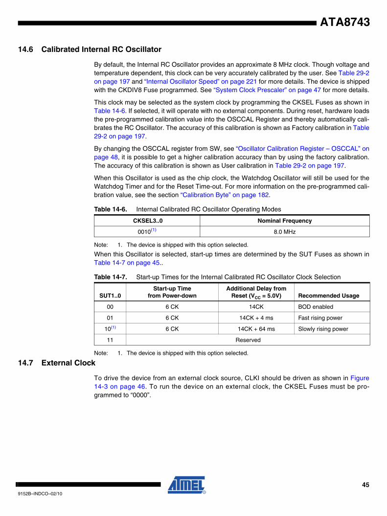
To drive the device from an external clock source, CLKI should be driven as shown in Figure14-3 on page 46. To run the device on an external clock, the CKSEL Fuses must be pro-grammed to “0000”.
Table 14-6. Internal Calibrated RC Oscillator Operating Modes
CKSEL3..0 Nominal Frequency
0010(1) 8.0 MHz
Table 14-7. Start-up Times for the Internal Calibrated RC Oscillator Clock Selection
SUT1..0Start-up Time
from Power-downAdditional Delay from
Reset (VCC = 5.0V) Recommended Usage
00 6 CK 14CK BOD enabled
01 6 CK 14CK + 4 ms Fast rising power
10(1) 6 CK 14CK + 64 ms Slowly rising power
11 Reserved
459152B–INDCO–02/10
Figure 14-3. External Clock Drive Configuration
When this clock source is selected, start-up times are determined by the SUT Fuses as shown inTable 14-8 on page 46.
When applying an external clock, it is required to avoid sudden changes in the applied clock fre-quency to ensure stable operation of the MCU. A variation in frequency of more than 2% fromone clock cycle to the next can lead to unpredictable behavior. It is required to ensure that theMCU is kept in Reset during such changes in the clock frequency.
Note that the System Clock Prescaler can be used to implement run-time changes of the internalclock frequency while still ensuring stable operation. See to “System Clock Prescaler” on page47 for details.
Table 14-8. Start-up Times for the External Clock Selection
SUT1..0Start-up Time from
Power-down and Power-saveAdditional Delay from
Reset Recommended Usage
00 6 CK 14CK BOD enabled
01 6 CK 14CK + 4 ms Fast rising power
10 6 CK 14CK + 64 ms Slowly rising power
11 Reserved
EXTERNALCLOCKSIGNAL
CLKI
GND
469152B–INDCO–02/10
ATA8743
ATA8743
14.8 128 kHz Internal Oscillator
The 128 kHz internal Oscillator is a low power Oscillator providing a clock of 128 kHz. The fre-quency is nominal at 3V and 25°C. This clock may be select as the system clock byprogramming the CKSEL Fuses to “0100”.
When this clock source is selected, start-up times are determined by the SUT Fuses as shown inTable 14-9 on page 47.
14.9 System Clock Prescaler
The ATtiny24/44/84 system clock can be divided by setting the Clock Prescale Register –CLKPR. This feature can be used to decrease power consumption when the requirement forprocessing power is low. This can be used with all clock source options, and it will affect theclock frequency of the CPU and all synchronous peripherals. clkI/O, clkADC, clkCPU, and clkFLASH
are divided by a factor as shown in Table 14-10 on page 49.
14.9.1 Switching Time
When switching between prescaler settings, the System Clock Prescaler ensures that noglitches occur in the clock system and that no intermediate frequency is higher than neither theclock frequency corresponding to the previous setting, nor the clock frequency corresponding tothe new setting.
The ripple counter that implements the prescaler runs at the frequency of the undivided clock,which may be faster than the CPU’s clock frequency. Hence, it is not possible to determine thestate of the prescaler – even if it were readable, and the exact time it takes to switch from oneclock division to another cannot be exactly predicted.
From the time the CLKPS values are written, it takes between T1 + T2 and T1 + 2*T2 before thenew clock frequency is active. In this interval, 2 active clock edges are produced. Here, T1 is theprevious clock period, and T2 is the period corresponding to the new prescaler setting.
Table 14-9. Start-up Times for the 128 kHz Internal Oscillator
SUT1..0Start-up Time from
Power-down and Power-saveAdditional Delay from
Reset Recommended Usage
00 6 CK 14CK BOD enabled
01 6 CK 14CK + 4 ms Fast rising power
10 6 CK 14CK + 64 ms Slowly rising power
11 Reserved
479152B–INDCO–02/10
14.10 Register Description
14.10.1 Oscillator Calibration Register – OSCCAL
The Oscillator Calibration Register is used to trim the Calibrated Internal RC Oscillator toremove process variations from the oscillator frequency. A pre-programmed calibration value isautomatically written to this register during chip reset, giving the Factory calibrated frequency asspecified in Table 29-2 on page 197. The application software can write this register to changethe oscillator frequency. The oscillator can be calibrated to frequencies as specified in Table29-2 on page 197. Calibration outside that range is not guaranteed.
Note that this oscillator is used to time EEPROM and Flash write accesses, and these writetimes will be affected accordingly. If the EEPROM or Flash are written, do not calibrate to morethan 8.8 MHz. Otherwise, the EEPROM or Flash write may fail.
The CAL7 bit determines the range of operation for the oscillator. Setting this bit to 0 gives thelowest frequency range, setting this bit to 1 gives the highest frequency range. The two fre-quency ranges are overlapping, in other words a setting of OSCCAL = 0x7F gives a higherfrequency than OSCCAL = 0x80.
The CAL6..0 bits are used to tune the frequency within the selected range. A setting of 0x00gives the lowest frequency in that range, and a setting of 0x7F gives the highest frequency in therange.
14.10.2 Clock Prescale Register – CLKPR
• Bit 7 – CLKPCE: Clock Prescaler Change EnableThe CLKPCE bit must be written to logic one to enable change of the CLKPS bits. The CLKPCEbit is only updated when the other bits in CLKPR are simultaneously written to zero. CLKPCE iscleared by hardware four cycles after it is written or when the CLKPS bits are written. Rewritingthe CLKPCE bit within this time-out period does neither extend the time-out period, nor clear theCLKPCE bit.
• Bits 6..4 – Res: Reserved BitsThese bits are reserved bits in the ATtiny24/44/84 and will always read as zero.
• Bits 3..0 – CLKPS3..0: Clock Prescaler Select Bits 3 - 0These bits define the division factor between the selected clock source and the internal systemclock. These bits can be written run-time to vary the clock frequency to suit the applicationrequirements. As the divider divides the master clock input to the MCU, the speed of all synchro-nous peripherals is reduced when a division factor is used. The division factors are given inTable 14-10 on page 49.
Bit 7 6 5 4 3 2 1 0
0x31 (0x51) CAL7 CAL6 CAL5 CAL4 CAL3 CAL2 CAL1 CAL0 OSCCAL
Read/Write R/W R/W R/W R/W R/W R/W R/W R/W
Initial Value Device Specific Calibration Value
Bit 7 6 5 4 3 2 1 0
0x26 (0x46) CLKPCE – – – CLKPS3 CLKPS2 CLKPS1 CLKPS0 CLKPR
Read/Write R/W R R R R/W R/W R/W R/W
Initial Value 0 0 0 0 See Bit Description
489152B–INDCO–02/10
ATA8743
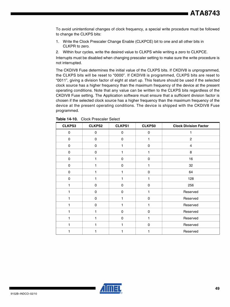
ATA8743
To avoid unintentional changes of clock frequency, a special write procedure must be followedto change the CLKPS bits:
1. Write the Clock Prescaler Change Enable (CLKPCE) bit to one and all other bits in CLKPR to zero.
2. Within four cycles, write the desired value to CLKPS while writing a zero to CLKPCE.
Interrupts must be disabled when changing prescaler setting to make sure the write procedure isnot interrupted.
The CKDIV8 Fuse determines the initial value of the CLKPS bits. If CKDIV8 is unprogrammed,the CLKPS bits will be reset to “0000”. If CKDIV8 is programmed, CLKPS bits are reset to“0011”, giving a division factor of eight at start up. This feature should be used if the selectedclock source has a higher frequency than the maximum frequency of the device at the presentoperating conditions. Note that any value can be written to the CLKPS bits regardless of theCKDIV8 Fuse setting. The Application software must ensure that a sufficient division factor ischosen if the selected clock source has a higher frequency than the maximum frequency of thedevice at the present operating conditions. The device is shipped with the CKDIV8 Fuseprogrammed.
Table 14-10. Clock Prescaler Select
CLKPS3 CLKPS2 CLKPS1 CLKPS0 Clock Division Factor
0 0 0 0 1
0 0 0 1 2
0 0 1 0 4
0 0 1 1 8
0 1 0 0 16
0 1 0 1 32
0 1 1 0 64
0 1 1 1 128
1 0 0 0 256
1 0 0 1 Reserved
1 0 1 0 Reserved
1 0 1 1 Reserved
1 1 0 0 Reserved
1 1 0 1 Reserved
1 1 1 0 Reserved
1 1 1 1 Reserved
499152B–INDCO–02/10
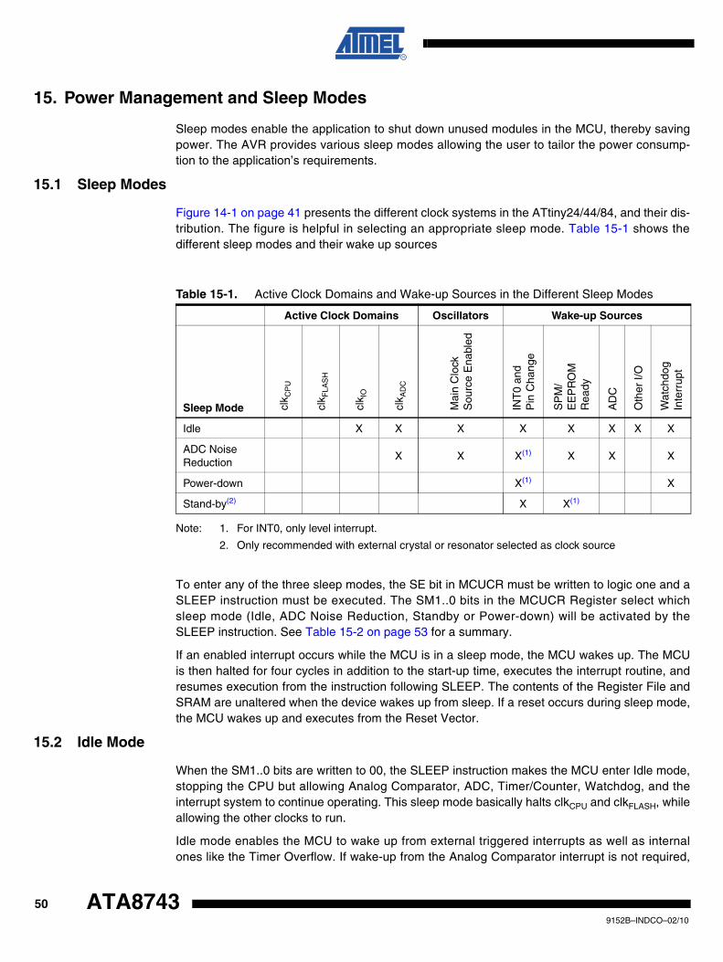
15. Power Management and Sleep Modes
Sleep modes enable the application to shut down unused modules in the MCU, thereby savingpower. The AVR provides various sleep modes allowing the user to tailor the power consump-tion to the application’s requirements.
15.1 Sleep Modes
Figure 14-1 on page 41 presents the different clock systems in the ATtiny24/44/84, and their dis-tribution. The figure is helpful in selecting an appropriate sleep mode. Table 15-1 shows thedifferent sleep modes and their wake up sources
Note: 1. For INT0, only level interrupt.
2. Only recommended with external crystal or resonator selected as clock source
To enter any of the three sleep modes, the SE bit in MCUCR must be written to logic one and aSLEEP instruction must be executed. The SM1..0 bits in the MCUCR Register select whichsleep mode (Idle, ADC Noise Reduction, Standby or Power-down) will be activated by theSLEEP instruction. See Table 15-2 on page 53 for a summary.
If an enabled interrupt occurs while the MCU is in a sleep mode, the MCU wakes up. The MCUis then halted for four cycles in addition to the start-up time, executes the interrupt routine, andresumes execution from the instruction following SLEEP. The contents of the Register File andSRAM are unaltered when the device wakes up from sleep. If a reset occurs during sleep mode,the MCU wakes up and executes from the Reset Vector.
15.2 Idle Mode
When the SM1..0 bits are written to 00, the SLEEP instruction makes the MCU enter Idle mode,stopping the CPU but allowing Analog Comparator, ADC, Timer/Counter, Watchdog, and theinterrupt system to continue operating. This sleep mode basically halts clkCPU and clkFLASH, whileallowing the other clocks to run.
Idle mode enables the MCU to wake up from external triggered interrupts as well as internalones like the Timer Overflow. If wake-up from the Analog Comparator interrupt is not required,
Table 15-1. Active Clock Domains and Wake-up Sources in the Different Sleep Modes
Active Clock Domains Oscillators Wake-up Sources
Sleep Mode clk C
PU
clk F
LAS
H
clk I
O
clk A
DC
Mai
n C
lock
S
ourc
e E
nabl
ed
INT
0 an
d P
in C
hang
e
SP
M/
EE
PR
OM
Rea
dy
AD
C
Oth
er I/
O
Wat
chdo
g In
terr
upt
Idle X X X X X X X X
ADC NoiseReduction
X X X(1) X X X
Power-down X(1) X
Stand-by(2) X X(1)
509152B–INDCO–02/10
ATA8743
ATA8743
the Analog Comparator can be powered down by setting the ACD bit in the Analog ComparatorControl and Status Register – ACSR. This will reduce power consumption in Idle mode. If theADC is enabled, a conversion starts automatically when this mode is entered.
15.3 ADC Noise Reduction Mode
When the SM1..0 bits are written to 01, the SLEEP instruction makes the MCU enter ADC NoiseReduction mode, stopping the CPU but allowing the ADC, the external interrupts, and theWatchdog to continue operating (if enabled). This sleep mode halts clkI/O, clkCPU, and clkFLASH,while allowing the other clocks to run.
This improves the noise environment for the ADC, enabling higher resolution measurements. Ifthe ADC is enabled, a conversion starts automatically when this mode is entered. Apart form theADC Conversion Complete interrupt, only an External Reset, a Watchdog Reset, a Brown-outReset, an SPM/EEPROM ready interrupt, an external level interrupt on INT0 or a pin changeinterrupt can wake up the MCU from ADC Noise Reduction mode.
15.4 Power-down Mode
When the SM1..0 bits are written to 10, the SLEEP instruction makes the MCU enterPower-down mode. In this mode, the Oscillator is stopped, while the external interrupts, and theWatchdog continue operating (if enabled). Only an External Reset, a Watchdog Reset, aBrown-out Reset, an external level interrupt on INT0, or a pin change interrupt can wake up theMCU. This sleep mode halts all generated clocks, allowing operation of asynchronous modulesonly.
Note that if a level triggered interrupt is used for wake-up from Power-down mode, the changedlevel must be held for some time to wake up the MCU. See “External Interrupts” on page 68 fordetails
15.5 Standby Mode
When the SM1..0 bits are 11 and an external crystal/resonator clock option is selected, theSLEEP instruction makes the MCU enter Standby mode. This mode is identical to Power-downwith the exception that the Oscillator is kept running. From Standby mode, the device wakes upin six clock cycles.
15.6 Power Reduction Register
The Power Reduction Register (PRR), see “PRR – Power Reduction Register” on page 54, pro-vides a method to stop the clock to individual peripherals to reduce power consumption. Thecurrent state of the peripheral is frozen and the I/O registers can not be read or written.Resources used by the peripheral when stopping the clock will remain occupied, hence theperipheral should in most cases be disabled before stopping the clock. Waking up a module,which is done by clearing the bit in PRR, puts the module in the same state as before shutdown.
Module shutdown can be used in Idle mode and Active mode to significantly reduce the overallpower consumption. See “Power-down Supply Current” on page 212 for examples. In all othersleep modes, the clock is already stopped.
519152B–INDCO–02/10
15.7 Minimizing Power Consumption
There are several issues to consider when trying to minimize the power consumption in an AVRcontrolled system. In general, sleep modes should be used as much as possible, and the sleepmode should be selected so that as few as possible of the device’s functions are operating. Allfunctions not needed should be disabled. In particular, the following modules may need specialconsideration when trying to achieve the lowest possible power consumption.
15.7.1 Analog to Digital Converter
If enabled, the ADC will be enabled in all sleep modes. To save power, the ADC should be dis-abled before entering any sleep mode. When the ADC is turned off and on again, the nextconversion will be an extended conversion. See “Analog to Digital Converter” on page 154 fordetails on ADC operation.
15.7.2 Analog Comparator
When entering Idle mode, the Analog Comparator should be disabled if not used. When enteringADC Noise Reduction mode, the Analog Comparator should be disabled. In the other sleepmodes, the Analog Comparator is automatically disabled. However, if the Analog Comparator isset up to use the Internal Voltage Reference as input, the Analog Comparator should be dis-abled in all sleep modes. Otherwise, the Internal Voltage Reference will be enabled,independent of sleep mode. See “Analog Comparator” on page 150 for details on how to config-ure the Analog Comparator.
15.7.3 Brown-out Detector
If the Brown-out Detector is not needed in the application, this module should be turned off. If theBrown-out Detector is enabled by the BODLEVEL Fuses, it will be enabled in all sleep modes,and hence, always consume power. In the deeper sleep modes, this will contribute significantlyto the total current consumption. See “Brown-out Detection” on page 59 for details on how toconfigure the Brown-out Detector.
15.7.4 Internal Voltage Reference
The Internal Voltage Reference will be enabled when needed by the Brown-out Detection, theAnalog Comparator or the ADC. If these modules are disabled as described in the sectionsabove, the internal voltage reference will be disabled and it will not be consuming power. Whenturned on again, the user must allow the reference to start up before the output is used. If thereference is kept on in sleep mode, the output can be used immediately. See “Internal VoltageReference” on page 60 for details on the start-up time.
15.7.5 Watchdog Timer
If the Watchdog Timer is not needed in the application, this module should be turned off. If theWatchdog Timer is enabled, it will be enabled in all sleep modes, and hence, always consumepower. In the deeper sleep modes, this will contribute significantly to the total current consump-tion. See “Watchdog Timer” on page 60 for details on how to configure the Watchdog Timer.
15.7.6 Port Pins
When entering a sleep mode, all port pins should be configured to use minimum power. Themost important thing is then to ensure that no pins drive resistive loads. In sleep modes whereboth the I/O clock (clkI/O) and the ADC clock (clkADC) are stopped, the input buffers of the devicewill be disabled. This ensures that no power is consumed by the input logic when not needed. In
529152B–INDCO–02/10
ATA8743
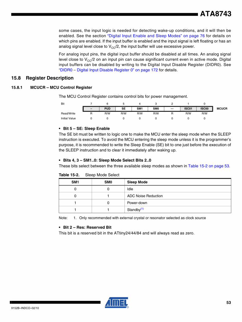
ATA8743
some cases, the input logic is needed for detecting wake-up conditions, and it will then beenabled. See the section “Digital Input Enable and Sleep Modes” on page 76 for details onwhich pins are enabled. If the input buffer is enabled and the input signal is left floating or has ananalog signal level close to VCC/2, the input buffer will use excessive power.
For analog input pins, the digital input buffer should be disabled at all times. An analog signallevel close to VCC/2 on an input pin can cause significant current even in active mode. Digitalinput buffers can be disabled by writing to the Digital Input Disable Register (DIDR0). See“DIDR0 – Digital Input Disable Register 0” on page 172 for details.
15.8 Register Description
15.8.1 MCUCR – MCU Control Register
The MCU Control Register contains control bits for power management.
• Bit 5 – SE: Sleep EnableThe SE bit must be written to logic one to make the MCU enter the sleep mode when the SLEEPinstruction is executed. To avoid the MCU entering the sleep mode unless it is the programmer’spurpose, it is recommended to write the Sleep Enable (SE) bit to one just before the execution ofthe SLEEP instruction and to clear it immediately after waking up.
• Bits 4, 3 – SM1..0: Sleep Mode Select Bits 2..0These bits select between the three available sleep modes as shown in Table 15-2 on page 53.
Note: 1. Only recommended with external crystal or resonator selected as clock source
• Bit 2 – Res: Reserved BitThis bit is a reserved bit in the ATtiny24/44/84 and will always read as zero.
Bit 7 6 5 4 3 2 1 0
– PUD SE SM1 SM0 — ISC01 ISC00 MCUCR
Read/Write R R/W R/W R/W R/W R R/W R/W
Initial Value 0 0 0 0 0 0 0 0
Table 15-2. Sleep Mode Select
SM1 SM0 Sleep Mode
0 0 Idle
0 1 ADC Noise Reduction
1 0 Power-down
1 1 Standby(1)
539152B–INDCO–02/10
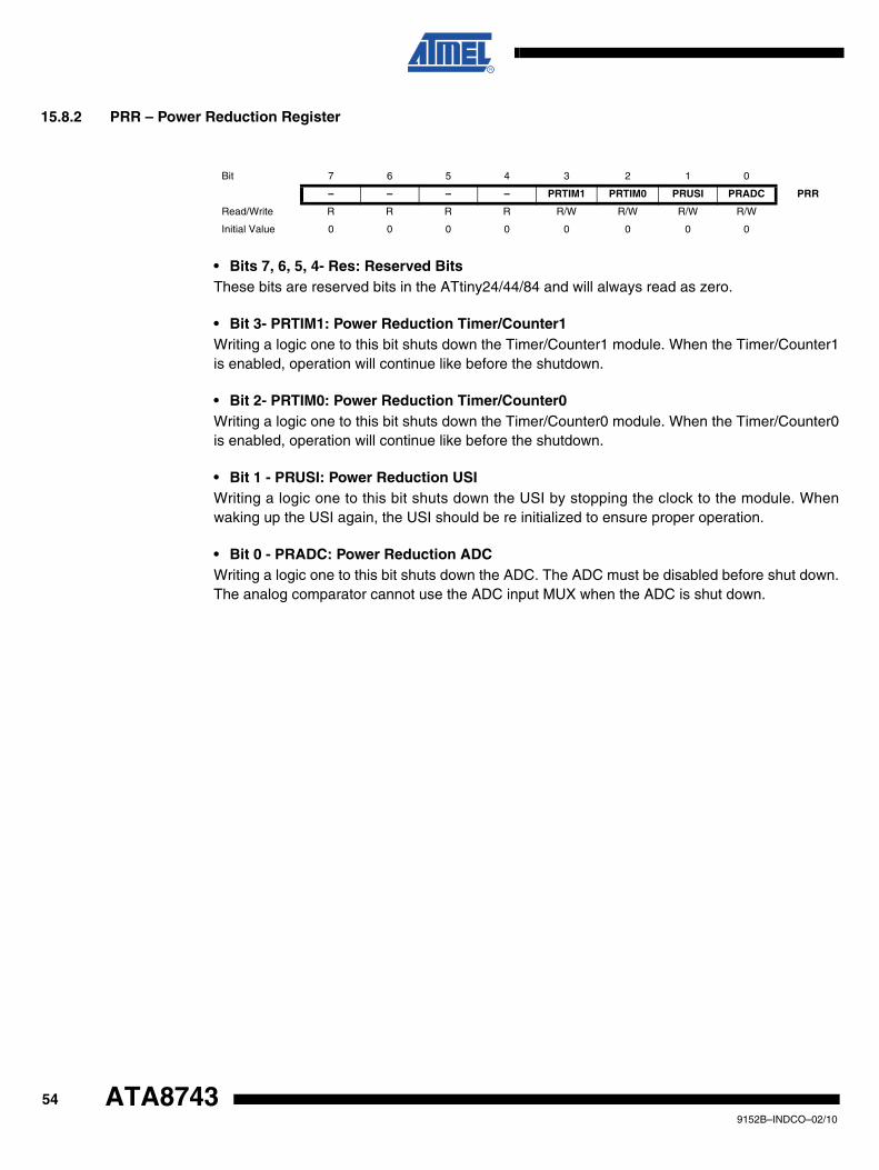
15.8.2 PRR – Power Reduction Register
• Bits 7, 6, 5, 4- Res: Reserved BitsThese bits are reserved bits in the ATtiny24/44/84 and will always read as zero.
• Bit 3- PRTIM1: Power Reduction Timer/Counter1Writing a logic one to this bit shuts down the Timer/Counter1 module. When the Timer/Counter1is enabled, operation will continue like before the shutdown.
• Bit 2- PRTIM0: Power Reduction Timer/Counter0Writing a logic one to this bit shuts down the Timer/Counter0 module. When the Timer/Counter0is enabled, operation will continue like before the shutdown.
• Bit 1 - PRUSI: Power Reduction USIWriting a logic one to this bit shuts down the USI by stopping the clock to the module. Whenwaking up the USI again, the USI should be re initialized to ensure proper operation.
• Bit 0 - PRADC: Power Reduction ADCWriting a logic one to this bit shuts down the ADC. The ADC must be disabled before shut down.The analog comparator cannot use the ADC input MUX when the ADC is shut down.
Bit 7 6 5 4 3 2 1 0
– – – – PRTIM1 PRTIM0 PRUSI PRADC PRR
Read/Write R R R R R/W R/W R/W R/W
Initial Value 0 0 0 0 0 0 0 0
549152B–INDCO–02/10
ATA8743
ATA8743
16. System Control and Reset
16.0.1 Resetting the AVR
During reset, all I/O Registers are set to their initial values, and the program starts executionfrom the Reset Vector. The instruction placed at the Reset Vector must be a RJMP – RelativeJump – instruction to the reset handling routine. If the program never enables an interruptsource, the Interrupt Vectors are not used, and regular program code can be placed at theselocations. The circuit diagram in Figure 16-1 on page 56 shows the reset logic. Table 16-1 onpage 57 defines the electrical parameters of the reset circuitry.
The I/O ports of the AVR are immediately reset to their initial state when a reset source goesactive. This does not require any clock source to be running.
After all reset sources have gone inactive, a delay counter is invoked, stretching the internalreset. This allows the power to reach a stable level before normal operation starts. The time-outperiod of the delay counter is defined by the user through the SUT and CKSEL Fuses. The dif-ferent selections for the delay period are presented in “Clock Sources” on page 42.
16.0.2 Reset Sources
The ATtiny24/44/84 has four sources of reset:
• Power-on Reset. The MCU is reset when the supply voltage is below the Power-on Reset threshold (VPOT).
• External Reset. The MCU is reset when a low level is present on the RESET pin for longer than the minimum pulse length when RESET function is enabled.
• Watchdog Reset. The MCU is reset when the Watchdog Timer period expires and the Watchdog is enabled.
• Brown-out Reset. The MCU is reset when the supply voltage VCC is below the Brown-out Reset threshold (VBOT) and the Brown-out Detector is enabled.
559152B–INDCO–02/10
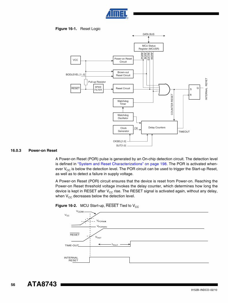
Figure 16-1. Reset Logic
16.0.3 Power-on Reset
A Power-on Reset (POR) pulse is generated by an On-chip detection circuit. The detection levelis defined in “System and Reset Characterizations” on page 198. The POR is activated when-ever VCC is below the detection level. The POR circuit can be used to trigger the Start-up Reset,as well as to detect a failure in supply voltage.
A Power-on Reset (POR) circuit ensures that the device is reset from Power-on. Reaching thePower-on Reset threshold voltage invokes the delay counter, which determines how long thedevice is kept in RESET after VCC rise. The RESET signal is activated again, without any delay,when VCC decreases below the detection level.
Figure 16-2. MCU Start-up, RESET Tied to VCC
MCU StatusRegister (MCUSR)
Brown-outReset CircuitBODLEVEL [1..0]
Delay Counters
CKSEL[1:0]
CKTIMEOUT
WD
RF
BO
RF
EX
TR
F
PO
RF
DATA BUS
ClockGenerator
SPIKEFILTER
Pull-up Resistor
WatchdogOscillator
SUT[1:0]
Power-on ResetCircuit
RESET
TIME-OUT
INTERNALRESET
tTOUT
VRST
VPORMAX
VCC
CCRRV
VPORMIN
569152B–INDCO–02/10
ATA8743
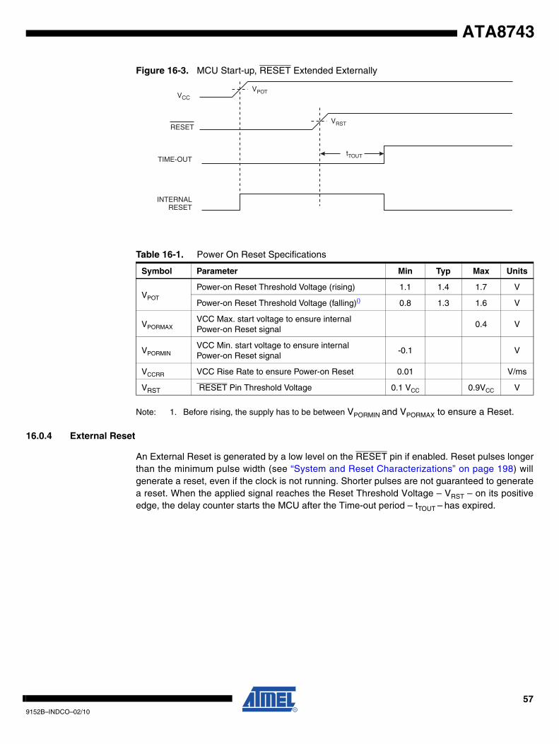
ATA8743
Figure 16-3. MCU Start-up, RESET Extended Externally
Note: 1. Before rising, the supply has to be between VPORMIN and VPORMAX to ensure a Reset.
16.0.4 External Reset
An External Reset is generated by a low level on the RESET pin if enabled. Reset pulses longerthan the minimum pulse width (see “System and Reset Characterizations” on page 198) willgenerate a reset, even if the clock is not running. Shorter pulses are not guaranteed to generatea reset. When the applied signal reaches the Reset Threshold Voltage – VRST – on its positiveedge, the delay counter starts the MCU after the Time-out period – tTOUT – has expired.
Table 16-1. Power On Reset Specifications
Symbol Parameter Min Typ Max Units
VPOT
Power-on Reset Threshold Voltage (rising) 1.1 1.4 1.7 V
Power-on Reset Threshold Voltage (falling)() 0.8 1.3 1.6 V
VPORMAXVCC Max. start voltage to ensure internal Power-on Reset signal
0.4 V
VPORMINVCC Min. start voltage to ensure internal Power-on Reset signal
-0.1 V
VCCRR VCC Rise Rate to ensure Power-on Reset 0.01 V/ms
VRST RESET Pin Threshold Voltage 0.1 VCC 0.9VCC V
RESET
TIME-OUT
INTERNALRESET
tTOUT
VPOT
VRST
VCC
579152B–INDCO–02/10
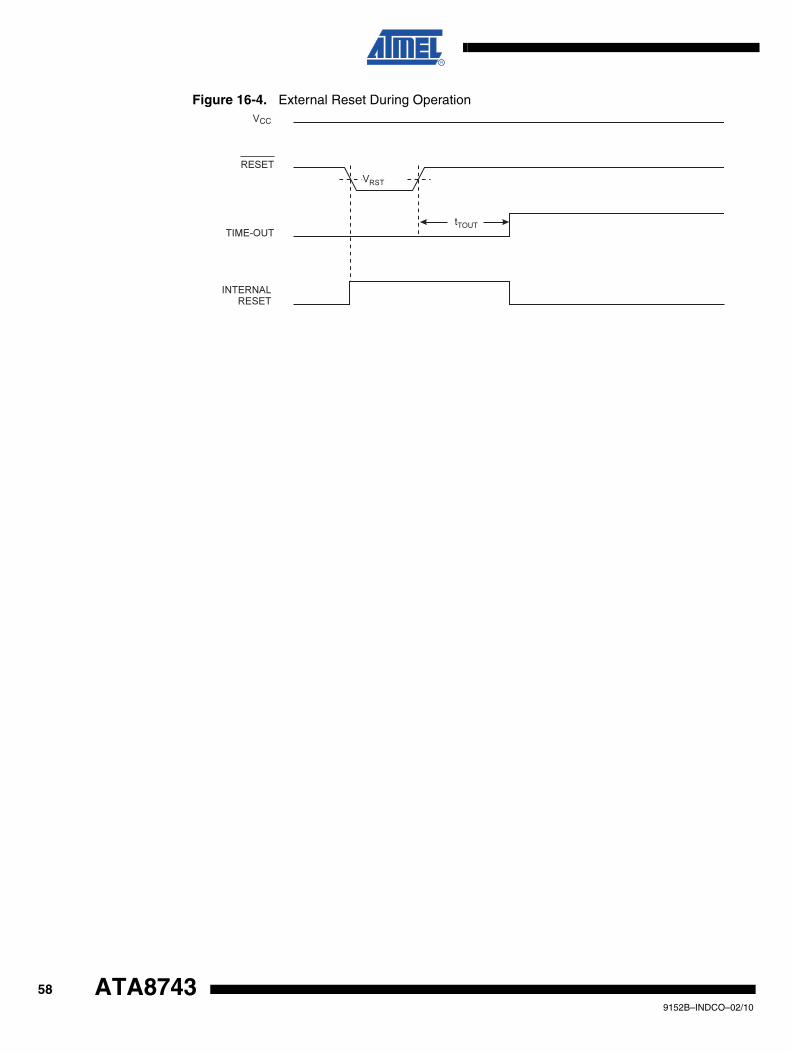
Figure 16-4. External Reset During Operation
CC
589152B–INDCO–02/10
ATA8743
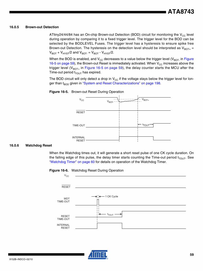
ATA8743
16.0.5 Brown-out Detection
ATtiny24/44/84 has an On-chip Brown-out Detection (BOD) circuit for monitoring the VCC levelduring operation by comparing it to a fixed trigger level. The trigger level for the BOD can beselected by the BODLEVEL Fuses. The trigger level has a hysteresis to ensure spike freeBrown-out Detection. The hysteresis on the detection level should be interpreted as VBOT+ =VBOT + VHYST/2 and VBOT- = VBOT - VHYST/2.
When the BOD is enabled, and VCC decreases to a value below the trigger level (VBOT- in Figure16-5 on page 59), the Brown-out Reset is immediately activated. When VCC increases above thetrigger level (VBOT+ in Figure 16-5 on page 59), the delay counter starts the MCU after theTime-out period tTOUT has expired.
The BOD circuit will only detect a drop in VCC if the voltage stays below the trigger level for lon-ger than tBOD given in “System and Reset Characterizations” on page 198.
Figure 16-5. Brown-out Reset During Operation
16.0.6 Watchdog Reset
When the Watchdog times out, it will generate a short reset pulse of one CK cycle duration. Onthe falling edge of this pulse, the delay timer starts counting the Time-out period tTOUT. See“Watchdog Timer” on page 60 for details on operation of the Watchdog Timer.
Figure 16-6. Watchdog Reset During Operation
VCC
RESET
TIME-OUT
INTERNALRESET
VBOT-VBOT+
tTOUT
CK
CC
599152B–INDCO–02/10
16.1 Internal Voltage Reference
ATtiny24/44/84 features an internal bandgap reference. This reference is used for Brown-outDetection, and it can be used as an input to the Analog Comparator or the ADC.
16.1.1 Voltage Reference Enable Signals and Start-up Time
The voltage reference has a start-up time that may influence the way it should be used. Thestart-up time is given in “System and Reset Characterizations” on page 198. To save power, thereference is not always turned on. The reference is on during the following situations:
1. When the BOD is enabled (by programming the BODLEVEL [2..0] Fuse).
2. When the bandgap reference is connected to the Analog Comparator (by setting the ACBG bit in ACSR).
3. When the ADC is enabled.
Thus, when the BOD is not enabled, after setting the ACBG bit or enabling the ADC, the usermust always allow the reference to start up before the output from the Analog Comparator orADC is used. To reduce power consumption in Power-down mode, the user can avoid the threeconditions above to ensure that the reference is turned off before entering Power-down mode.
16.2 Watchdog Timer
The Watchdog Timer is clocked from an On-chip Oscillator which runs at 128 kHz. By controllingthe Watchdog Timer prescaler, the Watchdog Reset interval can be adjusted as shown in Table16-4 on page 64. The WDR – Watchdog Reset – instruction resets the Watchdog Timer. TheWatchdog Timer is also reset when it is disabled and when a Chip Reset occurs. Ten differentclock cycle periods can be selected to determine the reset period. If the reset period expireswithout another Watchdog Reset, the ATtiny24/44/84 resets and executes from the Reset Vec-tor. For timing details on the Watchdog Reset, refer to Table 16-4 on page 64.
The watchdog Timer can also be configured to generate an interrupt instead of a reset. This canbe very helpful when using the Watchdog to wake-up from Power-down.
To prevent unintentional disabling of the Watchdog or unintentional change of time-out period,two different safety levels are selected by the fuse WDTON as shown in Table 16-2. See “TimedSequences for Changing the Configuration of the Watchdog Timer” on page 61 for details.
Table 16-2. WDT Configuration as a Function of the Fuse Settings of WDTON
WDTONSafety Level
WDT Initial State
How to Disable the WDT
How to Change Time-out
Unprogrammed 1 Disabled Timed sequence No limitations
Programmed 2 Enabled Always enabled Timed sequence
609152B–INDCO–02/10
ATA8743
ATA8743
Figure 16-7. Watchdog Timer
16.3 Timed Sequences for Changing the Configuration of the Watchdog Timer
The sequence for changing configuration differs slightly between the two safety levels. Separateprocedures are described for each level.
16.3.1 Safety Level 1
In this mode, the Watchdog Timer is initially disabled, but can be enabled by writing the WDE bitto one without any restriction. A timed sequence is needed when disabling an enabled Watch-dog Timer. To disable an enabled Watchdog Timer, the following procedure must be followed:
1. In the same operation, write a logic one to WDCE and WDE. A logic one must be written to WDE regardless of the previous value of the WDE bit.
2. Within the next four clock cycles, in the same operation, write the WDE and WDP bits as desired, but with the WDCE bit cleared.
16.3.2 Safety Level 2
In this mode, the Watchdog Timer is always enabled, and the WDE bit will always read as one. Atimed sequence is needed when changing the Watchdog Time-out period. To change theWatchdog Time-out, the following procedure must be followed:
1. In the same operation, write a logical one to WDCE and WDE. Even though the WDE always is set, the WDE must be written to one to start the timed sequence.
2. Within the next four clock cycles, in the same operation, write the WDP bits as desired, but with the WDCE bit cleared. The value written to the WDE bit is irrelevant.
OS
C/2
K
OS
C/4
K
OS
C/8
K
OS
C/1
6K
OS
C/3
2K
OS
C/6
4K
OS
C/1
28K
OS
C/2
56K
OS
C/5
12K
OS
C/1
024K
MCU RESET
WATCHDOGPRESCALER
128 kHzOSCILLATOR
WATCHDOGRESET
WDP0WDP1WDP2WDP3
WDE
619152B–INDCO–02/10
16.4 Register Description
16.4.1 MCUSR – MCU Status Register
The MCU Status Register provides information on which reset source caused an MCU Reset.
• Bits 7..4 – Res: Reserved BitsThese bits are reserved bits in the ATtiny24/44/84 and will always read as zero.
• Bit 3 – WDRF: Watchdog Reset FlagThis bit is set if a Watchdog Reset occurs. The bit is reset by a Power-on Reset, or by writing alogic zero to the flag.
• Bit 2 – BORF: Brown-out Reset FlagThis bit is set if a Brown-out Reset occurs. The bit is reset by a Power-on Reset, or by writing alogic zero to the flag.
• Bit 1 – EXTRF: External Reset FlagThis bit is set if an External Reset occurs. The bit is reset by a Power-on Reset, or by writing alogic zero to the flag.
• Bit 0 – PORF: Power-on Reset FlagThis bit is set if a Power-on Reset occurs. The bit is reset only by writing a logic zero to the flag.
To make use of the Reset Flags to identify a reset condition, the user should read and then resetthe MCUSR as early as possible in the program. If the register is cleared before another resetoccurs, the source of the reset can be found by examining the Reset Flags.
16.4.2 WDTCSR – Watchdog Timer Control and Status Register
• Bit 7 – WDIF: Watchdog Timeout Interrupt FlagThis bit is set when a time-out occurs in the Watchdog Timer and the Watchdog Timer is config-ured for interrupt. WDIF is cleared by hardware when executing the corresponding interrupthandling vector. Alternatively, WDIF is cleared by writing a logic one to the flag. When the I-bit inSREG and WDIE are set, the Watchdog Time-out Interrupt is executed.
• Bit 6 – WDIE: Watchdog Timeout Interrupt EnableWhen this bit is written to one, WDE is cleared, and the I-bit in the Status Register is set, theWatchdog Time-out Interrupt is enabled. In this mode the corresponding interrupt is executedinstead of a reset if a timeout in the Watchdog Timer occurs.
If WDE is set, WDIE is automatically cleared by hardware when a time-out occurs. This is usefulfor keeping the Watchdog Reset security while using the interrupt. After the WDIE bit is cleared,
Bit 7 6 5 4 3 2 1 0
0x34 (0x54) – – – – WDRF BORF EXTRF PORF MCUSR
Read/Write R R R R R/W R/W R/W R/W
Initial Value 0 0 0 0 See Bit Description
Bit 7 6 5 4 3 2 1 0
0x21 (0x41) WDIF WDIE WDP3 WDCE WDE WDP2 WDP1 WDP0 WDTCSR
Read/Write R/W R/W R/W R/W R/W R/W R/W R/W
Initial Value 0 0 0 0 X 0 0 0
629152B–INDCO–02/10
ATA8743
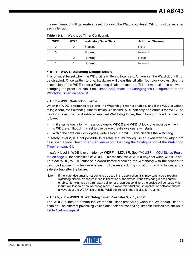
ATA8743
the next time-out will generate a reset. To avoid the Watchdog Reset, WDIE must be set aftereach interrupt.
• Bit 4 – WDCE: Watchdog Change EnableThis bit must be set when the WDE bit is written to logic zero. Otherwise, the Watchdog will notbe disabled. Once written to one, hardware will clear this bit after four clock cycles. See thedescription of the WDE bit for a Watchdog disable procedure. This bit must also be set whenchanging the prescaler bits. See “Timed Sequences for Changing the Configuration of theWatchdog Timer” on page 61.
• Bit 3 – WDE: Watchdog EnableWhen the WDE is written to logic one, the Watchdog Timer is enabled, and if the WDE is writtento logic zero, the Watchdog Timer function is disabled. WDE can only be cleared if the WDCE bithas logic level one. To disable an enabled Watchdog Timer, the following procedure must befollowed:
1. In the same operation, write a logic one to WDCE and WDE. A logic one must be written to WDE even though it is set to one before the disable operation starts.
2. Within the next four clock cycles, write a logic 0 to WDE. This disables the Watchdog.
In safety level 2, it is not possible to disable the Watchdog Timer, even with the algorithmdescribed above. See “Timed Sequences for Changing the Configuration of the WatchdogTimer” on page 61.
In safety level 1, WDE is overridden by WDRF in MCUSR. See “MCUSR – MCU Status Regis-ter” on page 62 for description of WDRF. This means that WDE is always set when WDRF is set.To clear WDE, WDRF must be cleared before disabling the Watchdog with the proceduredescribed above. This feature ensures multiple resets during conditions causing failure, and asafe start-up after the failure.
Note: If the watchdog timer is not going to be used in the application, it is important to go through a watchdog disable procedure in the initialization of the device. If the Watchdog is accidentally enabled, for example by a runaway pointer or brown-out condition, the device will be reset, which in turn will lead to a new watchdog reset. To avoid this situation, the application software should always clear the WDRF flag and the WDE control bit in the initialization routine.
• Bits 5, 2..0 – WDP3..0: Watchdog Timer Prescaler 3, 2, 1, and 0The WDP3..0 bits determine the Watchdog Timer prescaling when the Watchdog Timer isenabled. The different prescaling values and their corresponding Timeout Periods are shown inTable 16-4 on page 64.
Table 16-3. Watchdog Timer Configuration
WDE WDIE Watchdog Timer State Action on Time-out
0 0 Stopped None
0 1 Running Interrupt
1 0 Running Reset
1 1 Running Interrupt
639152B–INDCO–02/10
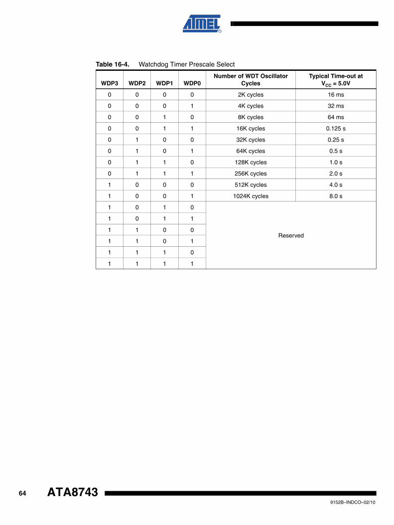
Table 16-4. Watchdog Timer Prescale Select
WDP3 WDP2 WDP1 WDP0Number of WDT Oscillator
CyclesTypical Time-out at
VCC = 5.0V
0 0 0 0 2K cycles 16 ms
0 0 0 1 4K cycles 32 ms
0 0 1 0 8K cycles 64 ms
0 0 1 1 16K cycles 0.125 s
0 1 0 0 32K cycles 0.25 s
0 1 0 1 64K cycles 0.5 s
0 1 1 0 128K cycles 1.0 s
0 1 1 1 256K cycles 2.0 s
1 0 0 0 512K cycles 4.0 s
1 0 0 1 1024K cycles 8.0 s
1 0 1 0
Reserved
1 0 1 1
1 1 0 0
1 1 0 1
1 1 1 0
1 1 1 1
649152B–INDCO–02/10
ATA8743
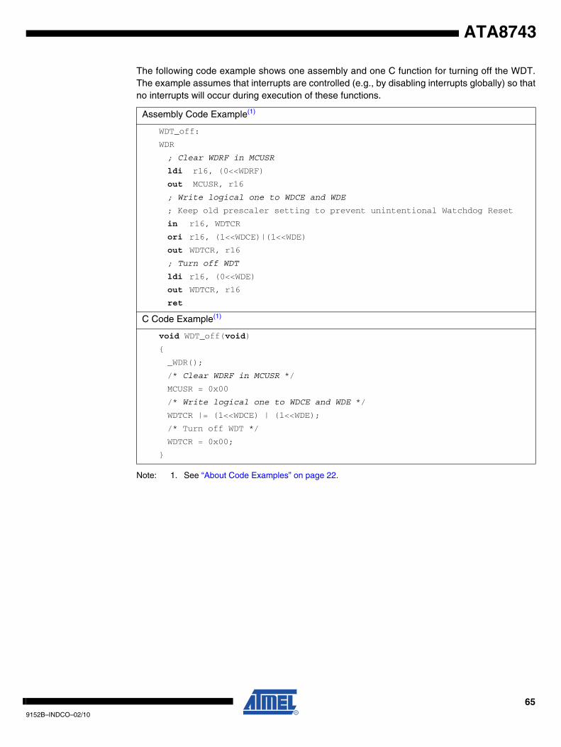
ATA8743
The following code example shows one assembly and one C function for turning off the WDT.The example assumes that interrupts are controlled (e.g., by disabling interrupts globally) so thatno interrupts will occur during execution of these functions.
Note: 1. See “About Code Examples” on page 22.
Assembly Code Example(1)
WDT_off:
WDR
; Clear WDRF in MCUSR
ldi r16, (0<<WDRF)
out MCUSR, r16
; Write logical one to WDCE and WDE
; Keep old prescaler setting to prevent unintentional Watchdog Reset
in r16, WDTCR
ori r16, (1<<WDCE)|(1<<WDE)
out WDTCR, r16
; Turn off WDT
ldi r16, (0<<WDE)
out WDTCR, r16
ret
C Code Example(1)
void WDT_off(void)
{
_WDR();
/* Clear WDRF in MCUSR */
MCUSR = 0x00
/* Write logical one to WDCE and WDE */
WDTCR |= (1<<WDCE) | (1<<WDE);
/* Turn off WDT */
WDTCR = 0x00;
}
659152B–INDCO–02/10
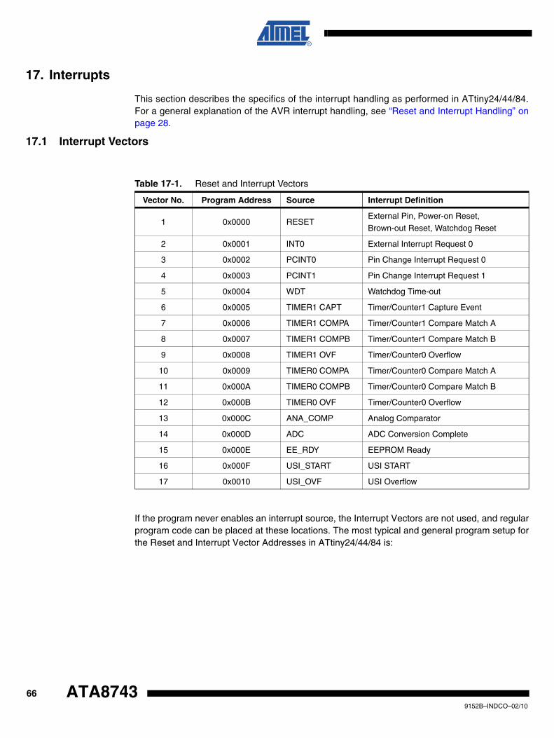
17. Interrupts
This section describes the specifics of the interrupt handling as performed in ATtiny24/44/84.For a general explanation of the AVR interrupt handling, see “Reset and Interrupt Handling” onpage 28.
17.1 Interrupt Vectors
If the program never enables an interrupt source, the Interrupt Vectors are not used, and regularprogram code can be placed at these locations. The most typical and general program setup forthe Reset and Interrupt Vector Addresses in ATtiny24/44/84 is:
Table 17-1. Reset and Interrupt Vectors
Vector No. Program Address Source Interrupt Definition
1 0x0000 RESETExternal Pin, Power-on Reset,
Brown-out Reset, Watchdog Reset
2 0x0001 INT0 External Interrupt Request 0
3 0x0002 PCINT0 Pin Change Interrupt Request 0
4 0x0003 PCINT1 Pin Change Interrupt Request 1
5 0x0004 WDT Watchdog Time-out
6 0x0005 TIMER1 CAPT Timer/Counter1 Capture Event
7 0x0006 TIMER1 COMPA Timer/Counter1 Compare Match A
8 0x0007 TIMER1 COMPB Timer/Counter1 Compare Match B
9 0x0008 TIMER1 OVF Timer/Counter0 Overflow
10 0x0009 TIMER0 COMPA Timer/Counter0 Compare Match A
11 0x000A TIMER0 COMPB Timer/Counter0 Compare Match B
12 0x000B TIMER0 OVF Timer/Counter0 Overflow
13 0x000C ANA_COMP Analog Comparator
14 0x000D ADC ADC Conversion Complete
15 0x000E EE_RDY EEPROM Ready
16 0x000F USI_START USI START
17 0x0010 USI_OVF USI Overflow
669152B–INDCO–02/10
ATA8743
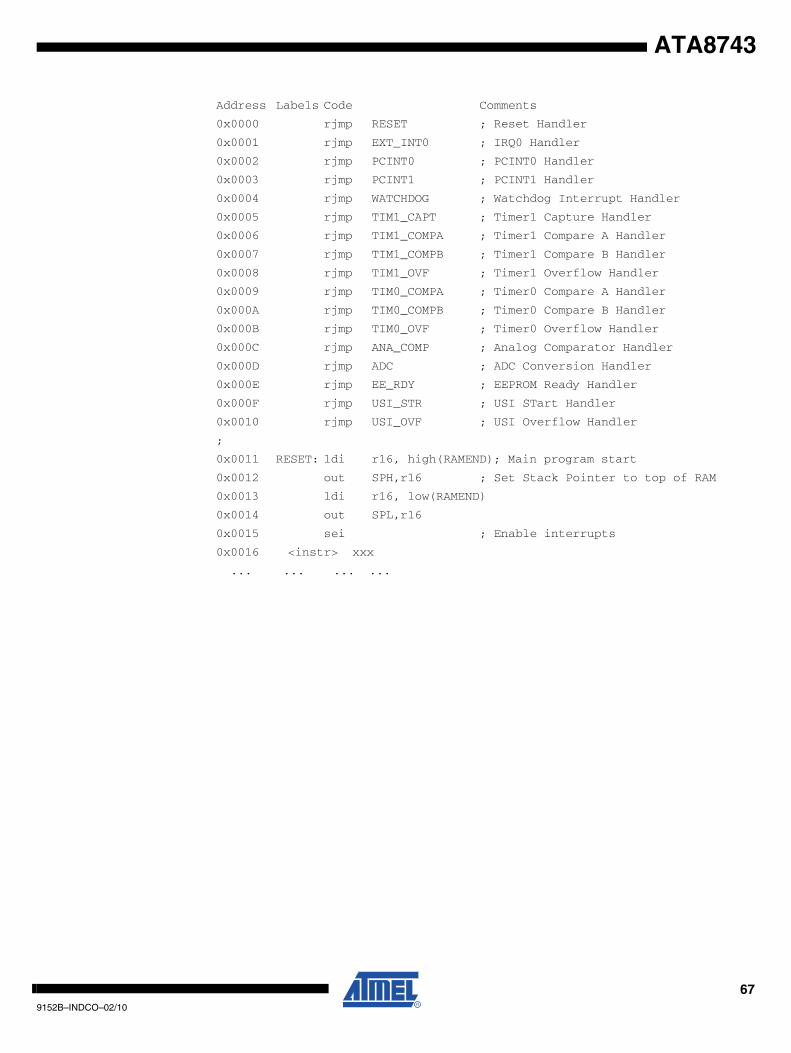
ATA8743
Address Labels Code Comments
0x0000 rjmp RESET ; Reset Handler
0x0001 rjmp EXT_INT0 ; IRQ0 Handler
0x0002 rjmp PCINT0 ; PCINT0 Handler
0x0003 rjmp PCINT1 ; PCINT1 Handler
0x0004 rjmp WATCHDOG ; Watchdog Interrupt Handler
0x0005 rjmp TIM1_CAPT ; Timer1 Capture Handler
0x0006 rjmp TIM1_COMPA ; Timer1 Compare A Handler
0x0007 rjmp TIM1_COMPB ; Timer1 Compare B Handler
0x0008 rjmp TIM1_OVF ; Timer1 Overflow Handler
0x0009 rjmp TIM0_COMPA ; Timer0 Compare A Handler
0x000A rjmp TIM0_COMPB ; Timer0 Compare B Handler
0x000B rjmp TIM0_OVF ; Timer0 Overflow Handler
0x000C rjmp ANA_COMP ; Analog Comparator Handler
0x000D rjmp ADC ; ADC Conversion Handler
0x000E rjmp EE_RDY ; EEPROM Ready Handler
0x000F rjmp USI_STR ; USI STart Handler
0x0010 rjmp USI_OVF ; USI Overflow Handler
;
0x0011 RESET: ldi r16, high(RAMEND); Main program start
0x0012 out SPH,r16 ; Set Stack Pointer to top of RAM
0x0013 ldi r16, low(RAMEND)
0x0014 out SPL,r16
0x0015 sei ; Enable interrupts
0x0016 <instr> xxx
... ... ... ...
679152B–INDCO–02/10
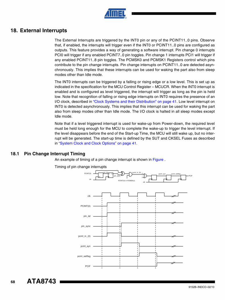
18. External Interrupts
The External Interrupts are triggered by the INT0 pin or any of the PCINT11..0 pins. Observethat, if enabled, the interrupts will trigger even if the INT0 or PCINT11..0 pins are configured asoutputs. This feature provides a way of generating a software interrupt. Pin change 0 interruptsPCI0 will trigger if any enabled PCINT7..0 pin toggles. Pin change 1 interrupts PCI1 will trigger ifany enabled PCINT11..8 pin toggles. The PCMSK0 and PCMSK1 Registers control which pinscontribute to the pin change interrupts. Pin change interrupts on PCINT11..0 are detected asyn-chronously. This implies that these interrupts can be used for waking the part also from sleepmodes other than Idle mode.
The INT0 interrupts can be triggered by a falling or rising edge or a low level. This is set up asindicated in the specification for the MCU Control Register – MCUCR. When the INT0 interrupt isenabled and is configured as level triggered, the interrupt will trigger as long as the pin is heldlow. Note that recognition of falling or rising edge interrupts on INT0 requires the presence of anI/O clock, described in “Clock Systems and their Distribution” on page 41. Low level interrupt onINT0 is detected asynchronously. This implies that this interrupt can be used for waking the partalso from sleep modes other than Idle mode. The I/O clock is halted in all sleep modes exceptIdle mode.
Note that if a level triggered interrupt is used for wake-up from Power-down, the required levelmust be held long enough for the MCU to complete the wake-up to trigger the level interrupt. Ifthe level disappears before the end of the Start-up Time, the MCU will still wake up, but no inter-rupt will be generated. The start-up time is defined by the SUT and CKSEL Fuses as describedin “System Clock and Clock Options” on page 41.
18.1 Pin Change Interrupt TimingAn example of timing of a pin change interrupt is shown in Figure .
Timing of pin change interrupts
clk
PCINT(0)
pin_lat
pin_sync
pcint_in_(0)
pcint_syn
pcint_setflag
PCIF
PCINT(0)
pin_syncpcint_syn
pin_latD Q
LE
pcint_setflagPCIF
clk
clkPCINT(0) in PCMSK(x)
pcint_in_(0) 0
x
689152B–INDCO–02/10
ATA8743
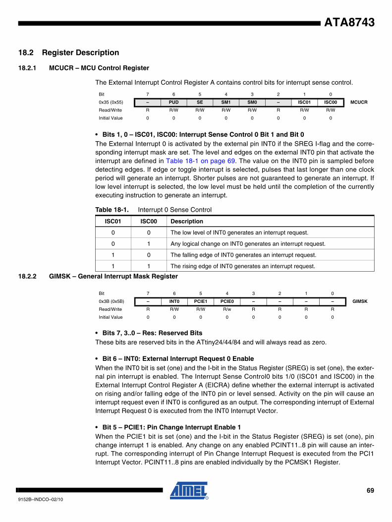
ATA8743
18.2 Register Description
18.2.1 MCUCR – MCU Control Register
The External Interrupt Control Register A contains control bits for interrupt sense control.
• Bits 1, 0 – ISC01, ISC00: Interrupt Sense Control 0 Bit 1 and Bit 0The External Interrupt 0 is activated by the external pin INT0 if the SREG I-flag and the corre-sponding interrupt mask are set. The level and edges on the external INT0 pin that activate theinterrupt are defined in Table 18-1 on page 69. The value on the INT0 pin is sampled beforedetecting edges. If edge or toggle interrupt is selected, pulses that last longer than one clockperiod will generate an interrupt. Shorter pulses are not guaranteed to generate an interrupt. Iflow level interrupt is selected, the low level must be held until the completion of the currentlyexecuting instruction to generate an interrupt.
18.2.2 GIMSK – General Interrupt Mask Register
• Bits 7, 3..0 – Res: Reserved BitsThese bits are reserved bits in the ATtiny24/44/84 and will always read as zero.
• Bit 6 – INT0: External Interrupt Request 0 EnableWhen the INT0 bit is set (one) and the I-bit in the Status Register (SREG) is set (one), the exter-nal pin interrupt is enabled. The Interrupt Sense Control0 bits 1/0 (ISC01 and ISC00) in theExternal Interrupt Control Register A (EICRA) define whether the external interrupt is activatedon rising and/or falling edge of the INT0 pin or level sensed. Activity on the pin will cause aninterrupt request even if INT0 is configured as an output. The corresponding interrupt of ExternalInterrupt Request 0 is executed from the INT0 Interrupt Vector.
• Bit 5 – PCIE1: Pin Change Interrupt Enable 1When the PCIE1 bit is set (one) and the I-bit in the Status Register (SREG) is set (one), pinchange interrupt 1 is enabled. Any change on any enabled PCINT11..8 pin will cause an inter-rupt. The corresponding interrupt of Pin Change Interrupt Request is executed from the PCI1Interrupt Vector. PCINT11..8 pins are enabled individually by the PCMSK1 Register.
Bit 7 6 5 4 3 2 1 0
0x35 (0x55) – PUD SE SM1 SM0 – ISC01 ISC00 MCUCR
Read/Write R R/W R/W R/W R/W R R/W R/W
Initial Value 0 0 0 0 0 0 0 0
Table 18-1. Interrupt 0 Sense Control
ISC01 ISC00 Description
0 0 The low level of INT0 generates an interrupt request.
0 1 Any logical change on INT0 generates an interrupt request.
1 0 The falling edge of INT0 generates an interrupt request.
1 1 The rising edge of INT0 generates an interrupt request.
Bit 7 6 5 4 3 2 1 0
0x3B (0x5B) – INT0 PCIE1 PCIE0 – – – – GIMSK
Read/Write R R/W R/W R/w R R R R
Initial Value 0 0 0 0 0 0 0 0
699152B–INDCO–02/10
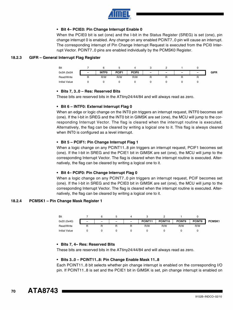
• Bit 4– PCIE0: Pin Change Interrupt Enable 0When the PCIE0 bit is set (one) and the I-bit in the Status Register (SREG) is set (one), pinchange interrupt 0 is enabled. Any change on any enabled PCINT7..0 pin will cause an interrupt.The corresponding interrupt of Pin Change Interrupt Request is executed from the PCI0 Inter-rupt Vector. PCINT7..0 pins are enabled individually by the PCMSK0 Register.
18.2.3 GIFR – General Interrupt Flag Register
• Bits 7, 3..0 – Res: Reserved BitsThese bits are reserved bits in the ATtiny24/44/84 and will always read as zero.
• Bit 6 – INTF0: External Interrupt Flag 0When an edge or logic change on the INT0 pin triggers an interrupt request, INTF0 becomes set(one). If the I-bit in SREG and the INT0 bit in GIMSK are set (one), the MCU will jump to the cor-responding Interrupt Vector. The flag is cleared when the interrupt routine is executed.Alternatively, the flag can be cleared by writing a logical one to it. This flag is always clearedwhen INT0 is configured as a level interrupt.
• Bit 5 – PCIF1: Pin Change Interrupt Flag 1When a logic change on any PCINT11..8 pin triggers an interrupt request, PCIF1 becomes set(one). If the I-bit in SREG and the PCIE1 bit in GIMSK are set (one), the MCU will jump to thecorresponding Interrupt Vector. The flag is cleared when the interrupt routine is executed. Alter-natively, the flag can be cleared by writing a logical one to it.
• Bit 4– PCIF0: Pin Change Interrupt Flag 0When a logic change on any PCINT7..0 pin triggers an interrupt request, PCIF becomes set(one). If the I-bit in SREG and the PCIE0 bit in GIMSK are set (one), the MCU will jump to thecorresponding Interrupt Vector. The flag is cleared when the interrupt routine is executed. Alter-natively, the flag can be cleared by writing a logical one to it.
18.2.4 PCMSK1 – Pin Change Mask Register 1
• Bits 7, 4– Res: Reserved BitsThese bits are reserved bits in the ATtiny24/44/84 and will always read as zero.
• Bits 3..0 – PCINT11..8: Pin Change Enable Mask 11..8Each PCINT11..8 bit selects whether pin change interrupt is enabled on the corresponding I/Opin. If PCINT11..8 is set and the PCIE1 bit in GIMSK is set, pin change interrupt is enabled on
Bit 7 6 5 4 3 2 1 0
0x3A (0x5A – INTF0 PCIF1 PCIF0 – – – – GIFR
Read/Write R R/W R/W R/W R R R R
Initial Value 0 0 0 0 0 0 0 0
Bit 7 6 5 4 3 2 1 0
0x20 (0x40) – – – – PCINT11 PCINT10 PCINT9 PCINT8 PCMSK1
Read/Write R R R R R/W R/W R/W R/W
Initial Value 0 0 0 0 0 0 0 0
709152B–INDCO–02/10
ATA8743
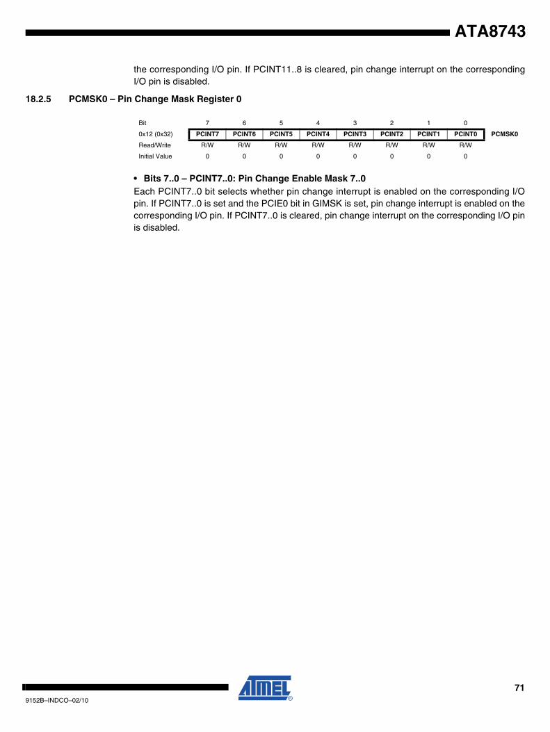
ATA8743
the corresponding I/O pin. If PCINT11..8 is cleared, pin change interrupt on the correspondingI/O pin is disabled.
18.2.5 PCMSK0 – Pin Change Mask Register 0
• Bits 7..0 – PCINT7..0: Pin Change Enable Mask 7..0Each PCINT7..0 bit selects whether pin change interrupt is enabled on the corresponding I/Opin. If PCINT7..0 is set and the PCIE0 bit in GIMSK is set, pin change interrupt is enabled on thecorresponding I/O pin. If PCINT7..0 is cleared, pin change interrupt on the corresponding I/O pinis disabled.
Bit 7 6 5 4 3 2 1 0
0x12 (0x32) PCINT7 PCINT6 PCINT5 PCINT4 PCINT3 PCINT2 PCINT1 PCINT0 PCMSK0
Read/Write R/W R/W R/W R/W R/W R/W R/W R/W
Initial Value 0 0 0 0 0 0 0 0
719152B–INDCO–02/10
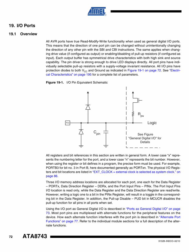
19. I/O Ports
19.1 Overview
All AVR ports have true Read-Modify-Write functionality when used as general digital I/O ports.This means that the direction of one port pin can be changed without unintentionally changingthe direction of any other pin with the SBI and CBI instructions. The same applies when chang-ing drive value (if configured as output) or enabling/disabling of pull-up resistors (if configured asinput). Each output buffer has symmetrical drive characteristics with both high sink and sourcecapability. The pin driver is strong enough to drive LED displays directly. All port pins have indi-vidually selectable pull-up resistors with a supply-voltage invariant resistance. All I/O pins haveprotection diodes to both VCC and Ground as indicated in Figure 19-1 on page 72. See “Electri-cal Characteristics” on page 195 for a complete list of parameters.
Figure 19-1. I/O Pin Equivalent Schematic
All registers and bit references in this section are written in general form. A lower case “x” repre-sents the numbering letter for the port, and a lower case “n” represents the bit number. However,when using the register or bit defines in a program, the precise form must be used. For example,PORTB3 for bit no. 3 in Port B, here documented generally as PORTxn. The physical I/O Regis-ters and bit locations are listed in “EXT_CLOCK = external clock is selected as system clock.” onpage 86.
Three I/O memory address locations are allocated for each port, one each for the Data Register– PORTx, Data Direction Register – DDRx, and the Port Input Pins – PINx. The Port Input PinsI/O location is read only, while the Data Register and the Data Direction Register are read/write.However, writing a logic one to a bit in the PINx Register, will result in a toggle in the correspond-ing bit in the Data Register. In addition, the Pull-up Disable – PUD bit in MCUCR disables thepull-up function for all pins in all ports when set.
Using the I/O port as General Digital I/O is described in “Ports as General Digital I/O” on page73. Most port pins are multiplexed with alternate functions for the peripheral features on thedevice. How each alternate function interferes with the port pin is described in “Alternate PortFunctions” on page 77. Refer to the individual module sections for a full description of the alter-nate functions.
Cpin
Logic
Rpu
See Figure"General Digital I/O" for
Details
Pxn
729152B–INDCO–02/10
ATA8743
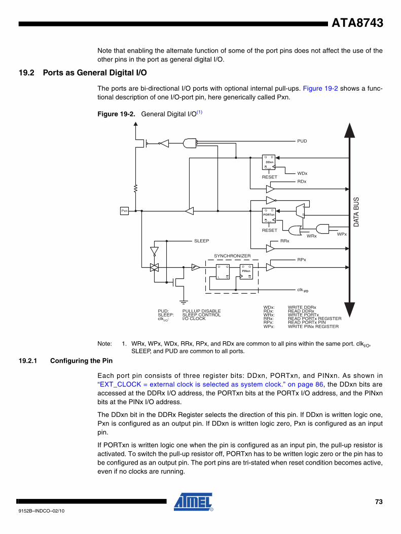
ATA8743
Note that enabling the alternate function of some of the port pins does not affect the use of theother pins in the port as general digital I/O.
19.2 Ports as General Digital I/O
The ports are bi-directional I/O ports with optional internal pull-ups. Figure 19-2 shows a func-tional description of one I/O-port pin, here generically called Pxn.
Figure 19-2. General Digital I/O(1)
Note: 1. WRx, WPx, WDx, RRx, RPx, and RDx are common to all pins within the same port. clkI/O, SLEEP, and PUD are common to all ports.
19.2.1 Configuring the Pin
Each port pin consists of three register bits: DDxn, PORTxn, and PINxn. As shown in“EXT_CLOCK = external clock is selected as system clock.” on page 86, the DDxn bits areaccessed at the DDRx I/O address, the PORTxn bits at the PORTx I/O address, and the PINxnbits at the PINx I/O address.
The DDxn bit in the DDRx Register selects the direction of this pin. If DDxn is written logic one,Pxn is configured as an output pin. If DDxn is written logic zero, Pxn is configured as an inputpin.
If PORTxn is written logic one when the pin is configured as an input pin, the pull-up resistor isactivated. To switch the pull-up resistor off, PORTxn has to be written logic zero or the pin has tobe configured as an output pin. The port pins are tri-stated when reset condition becomes active,even if no clocks are running.
clk
RPx
RRx
RDx
WDx
PUD
SYNCHRONIZER
WDx: WRITE DDRx
WRx: WRITE PORTxRRx: READ PORTx REGISTERRPx: READ PORTx PIN
PUD: PULLUP DISABLE
clkI/O: I/O CLOCK
RDx: READ DDRx
D
L
Q
Q
RESET
RESET
Q
QD
Q
Q D
CLR
PORTxn
Q
Q D
CLR
DDxn
PINxn
DAT
A B
US
SLEEP
SLEEP: SLEEP CONTROL
Pxn
I/O
WPx
0
1
WRx
WPx: WRITE PINx REGISTER
739152B–INDCO–02/10
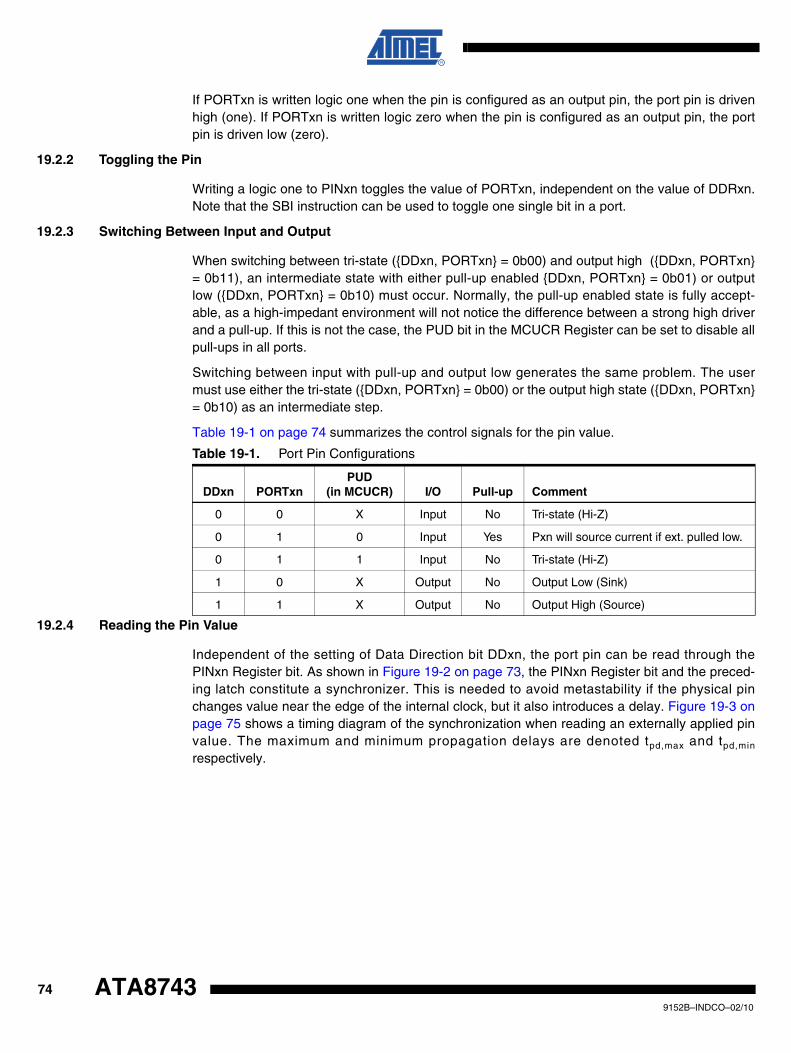
If PORTxn is written logic one when the pin is configured as an output pin, the port pin is drivenhigh (one). If PORTxn is written logic zero when the pin is configured as an output pin, the portpin is driven low (zero).
19.2.2 Toggling the Pin
Writing a logic one to PINxn toggles the value of PORTxn, independent on the value of DDRxn.Note that the SBI instruction can be used to toggle one single bit in a port.
19.2.3 Switching Between Input and Output
When switching between tri-state ({DDxn, PORTxn} = 0b00) and output high ({DDxn, PORTxn}= 0b11), an intermediate state with either pull-up enabled {DDxn, PORTxn} = 0b01) or outputlow ({DDxn, PORTxn} = 0b10) must occur. Normally, the pull-up enabled state is fully accept-able, as a high-impedant environment will not notice the difference between a strong high driverand a pull-up. If this is not the case, the PUD bit in the MCUCR Register can be set to disable allpull-ups in all ports.
Switching between input with pull-up and output low generates the same problem. The usermust use either the tri-state ({DDxn, PORTxn} = 0b00) or the output high state ({DDxn, PORTxn}= 0b10) as an intermediate step.
Table 19-1 on page 74 summarizes the control signals for the pin value.
19.2.4 Reading the Pin Value
Independent of the setting of Data Direction bit DDxn, the port pin can be read through thePINxn Register bit. As shown in Figure 19-2 on page 73, the PINxn Register bit and the preced-ing latch constitute a synchronizer. This is needed to avoid metastability if the physical pinchanges value near the edge of the internal clock, but it also introduces a delay. Figure 19-3 onpage 75 shows a timing diagram of the synchronization when reading an externally applied pinvalue. The maximum and minimum propagation delays are denoted tpd,max and tpd,min
respectively.
Table 19-1. Port Pin Configurations
DDxn PORTxnPUD
(in MCUCR) I/O Pull-up Comment
0 0 X Input No Tri-state (Hi-Z)
0 1 0 Input Yes Pxn will source current if ext. pulled low.
0 1 1 Input No Tri-state (Hi-Z)
1 0 X Output No Output Low (Sink)
1 1 X Output No Output High (Source)
749152B–INDCO–02/10
ATA8743
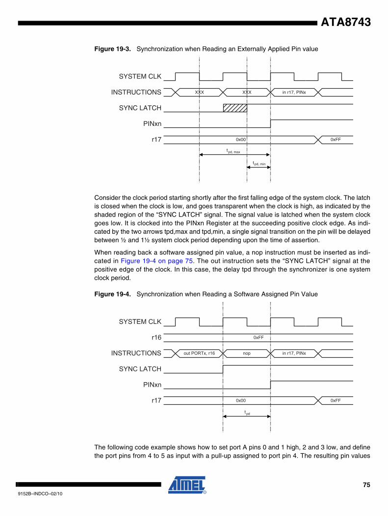
ATA8743
Figure 19-3. Synchronization when Reading an Externally Applied Pin value
Consider the clock period starting shortly after the first falling edge of the system clock. The latchis closed when the clock is low, and goes transparent when the clock is high, as indicated by theshaded region of the “SYNC LATCH” signal. The signal value is latched when the system clockgoes low. It is clocked into the PINxn Register at the succeeding positive clock edge. As indi-cated by the two arrows tpd,max and tpd,min, a single signal transition on the pin will be delayedbetween ½ and 1½ system clock period depending upon the time of assertion.
When reading back a software assigned pin value, a nop instruction must be inserted as indi-cated in Figure 19-4 on page 75. The out instruction sets the “SYNC LATCH” signal at thepositive edge of the clock. In this case, the delay tpd through the synchronizer is one systemclock period.
Figure 19-4. Synchronization when Reading a Software Assigned Pin Value
The following code example shows how to set port A pins 0 and 1 high, 2 and 3 low, and definethe port pins from 4 to 5 as input with a pull-up assigned to port pin 4. The resulting pin values
XXX in r17, PINx
0x00 0xFF
INSTRUCTIONS
SYNC LATCH
PINxn
r17
XXX
SYSTEM CLK
tpd, max
tpd, min
out PORTx, r16 nop in r17, PINx
0xFF
0x00 0xFF
SYSTEM CLK
r16
INSTRUCTIONS
SYNC LATCH
PINxn
r17tpd
759152B–INDCO–02/10
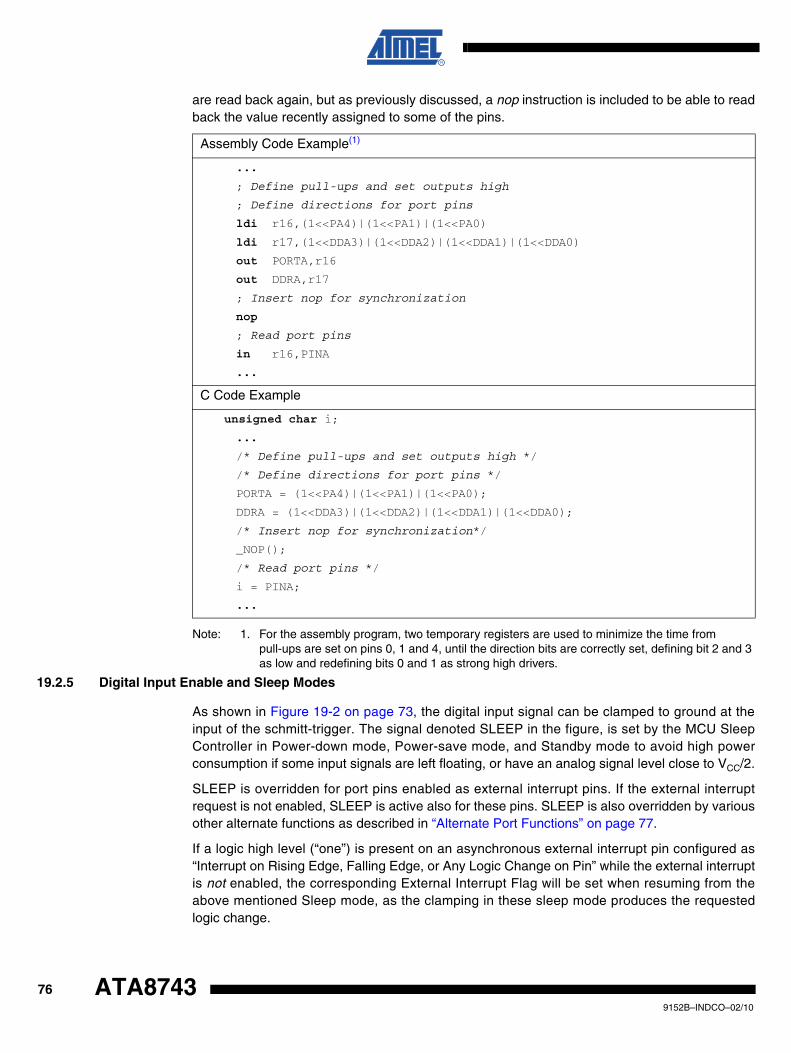
are read back again, but as previously discussed, a nop instruction is included to be able to readback the value recently assigned to some of the pins.
Note: 1. For the assembly program, two temporary registers are used to minimize the time from pull-ups are set on pins 0, 1 and 4, until the direction bits are correctly set, defining bit 2 and 3 as low and redefining bits 0 and 1 as strong high drivers.
19.2.5 Digital Input Enable and Sleep Modes
As shown in Figure 19-2 on page 73, the digital input signal can be clamped to ground at theinput of the schmitt-trigger. The signal denoted SLEEP in the figure, is set by the MCU SleepController in Power-down mode, Power-save mode, and Standby mode to avoid high powerconsumption if some input signals are left floating, or have an analog signal level close to VCC/2.
SLEEP is overridden for port pins enabled as external interrupt pins. If the external interruptrequest is not enabled, SLEEP is active also for these pins. SLEEP is also overridden by variousother alternate functions as described in “Alternate Port Functions” on page 77.
If a logic high level (“one”) is present on an asynchronous external interrupt pin configured as“Interrupt on Rising Edge, Falling Edge, or Any Logic Change on Pin” while the external interruptis not enabled, the corresponding External Interrupt Flag will be set when resuming from theabove mentioned Sleep mode, as the clamping in these sleep mode produces the requestedlogic change.
Assembly Code Example(1)
...
; Define pull-ups and set outputs high
; Define directions for port pins
ldi r16,(1<<PA4)|(1<<PA1)|(1<<PA0)
ldi r17,(1<<DDA3)|(1<<DDA2)|(1<<DDA1)|(1<<DDA0)
out PORTA,r16
out DDRA,r17
; Insert nop for synchronization
nop
; Read port pins
in r16,PINA
...
C Code Example
unsigned char i;
...
/* Define pull-ups and set outputs high */
/* Define directions for port pins */
PORTA = (1<<PA4)|(1<<PA1)|(1<<PA0);
DDRA = (1<<DDA3)|(1<<DDA2)|(1<<DDA1)|(1<<DDA0);
/* Insert nop for synchronization*/
_NOP();
/* Read port pins */
i = PINA;
...
769152B–INDCO–02/10
ATA8743
ATA8743
19.2.6 Unconnected Pins
If some pins are unused, it is recommended to ensure that these pins have a defined level. Eventhough most of the digital inputs are disabled in the deep sleep modes as described above, float-ing inputs should be avoided to reduce current consumption in all other modes where the digitalinputs are enabled (Reset, Active mode and Idle mode).
The simplest method to ensure a defined level of an unused pin, is to enable the internal pull-up.In this case, the pull-up will be disabled during reset. If low power consumption during reset isimportant, it is recommended to use an external pull-up or pulldown. Connecting unused pinsdirectly to VCC or GND is not recommended, since this may cause excessive currents if the pin isaccidentally configured as an output.
19.3 Alternate Port Functions
Most port pins have alternate functions in addition to being general digital I/Os. Figure 19-5 onpage 78 shows how the port pin control signals from the simplified Figure 19-2 on page 73 canbe overridden by alternate functions. The overriding signals may not be present in all port pins,but the figure serves as a generic description applicable to all port pins in the AVR microcon-troller family.
779152B–INDCO–02/10
Figure 19-5. Alternate Port Functions(1)
Note: 1. WRx, WPx, WDx, RRx, RPx, and RDx are common to all pins within the same port. clkI/O, SLEEP, and PUD are common to all ports. All other signals are unique for each pin.
Table 19-2 on page 79 summarizes the function of the overriding signals. The pin and portindexes from Figure 19-5 on page 78 are not shown in the succeeding tables. The overridingsignals are generated internally in the modules having the alternate function.
clk
RPx
RRxWRx
RDx
WDx
PUD
SYNCHRONIZER
WDx: WRITE DDRx
WRx: WRITE PORTxRRx: READ PORTx REGISTER
RPx: READ PORTx PIN
PUD: PULLUP DISABLE
clkI/O: I/O CLOCK
RDx: READ DDRx
D
L
Q
Q
SET
CLR
0
1
0
1
0
1
DIxn
AIOxn
DIEOExn
PVOVxn
PVOExn
DDOVxn
DDOExn
PUOExn
PUOVxn
PUOExn: Pxn PULL-UP OVERRIDE ENABLEPUOVxn: Pxn PULL-UP OVERRIDE VALUEDDOExn: Pxn DATA DIRECTION OVERRIDE ENABLEDDOVxn: Pxn DATA DIRECTION OVERRIDE VALUEPVOExn: Pxn PORT VALUE OVERRIDE ENABLEPVOVxn: Pxn PORT VALUE OVERRIDE VALUE
DIxn: DIGITAL INPUT PIN n ON PORTxAIOxn: ANALOG INPUT/OUTPUT PIN n ON PORTx
RESET
RESET
Q
Q D
CLR
Q
Q D
CLR
Q
QD
CLR
PINxn
PORTxn
DDxn
DAT
A B
US
0
1DIEOVxn
SLEEP
DIEOExn: Pxn DIGITAL INPUT-ENABLE OVERRIDE ENABLEDIEOVxn: Pxn DIGITAL INPUT-ENABLE OVERRIDE VALUESLEEP: SLEEP CONTROL
Pxn
I/O
0
1
PTOExn
PTOExn: Pxn, PORT TOGGLE OVERRIDE ENABLE
WPx: WRITE PINx
WPx
789152B–INDCO–02/10
ATA8743
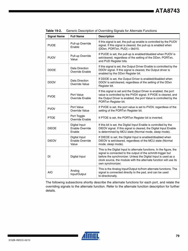
ATA8743
The following subsections shortly describe the alternate functions for each port, and relate theoverriding signals to the alternate function. Refer to the alternate function description for furtherdetails.
Table 19-2. Generic Description of Overriding Signals for Alternate Functions
Signal Name Full Name Description
PUOEPull-up Override Enable
If this signal is set, the pull-up enable is controlled by the PUOV signal. If this signal is cleared, the pull-up is enabled when {DDxn, PORTxn, PUD} = 0b010.
PUOVPull-up Override Value
If PUOE is set, the pull-up is enabled/disabled when PUOV is set/cleared, regardless of the setting of the DDxn, PORTxn, and PUD Register bits.
DDOEData Direction Override Enable
If this signal is set, the Output Driver Enable is controlled by the DDOV signal. If this signal is cleared, the Output driver is enabled by the DDxn Register bit.
DDOVData Direction Override Value
If DDOE is set, the Output Driver is enabled/disabled when DDOV is set/cleared, regardless of the setting of the DDxn Register bit.
PVOEPort Value Override Enable
If this signal is set and the Output Driver is enabled, the port value is controlled by the PVOV signal. If PVOE is cleared, and the Output Driver is enabled, the port Value is controlled by the PORTxn Register bit.
PVOVPort Value Override Value
If PVOE is set, the port value is set to PVOV, regardless of the setting of the PORTxn Register bit.
PTOEPort Toggle Override Enable
If PTOE is set, the PORTxn Register bit is inverted.
DIEOEDigital Input Enable Override Enable
If this bit is set, the Digital Input Enable is controlled by the DIEOV signal. If this signal is cleared, the Digital Input Enable is determined by MCU state (Normal mode, sleep mode).
DIEOVDigital Input Enable Override Value
If DIEOE is set, the Digital Input is enabled/disabled when DIEOV is set/cleared, regardless of the MCU state (Normal mode, sleep mode).
DI Digital Input
This is the Digital Input to alternate functions. In the figure, the signal is connected to the output of the schmitt-trigger but before the synchronizer. Unless the Digital Input is used as a clock source, the module with the alternate function will use its own synchronizer.
AIOAnalog Input/Output
This is the Analog Input/Output to/from alternate functions. The signal is connected directly to the pad, and can be used bi-directionally.
799152B–INDCO–02/10
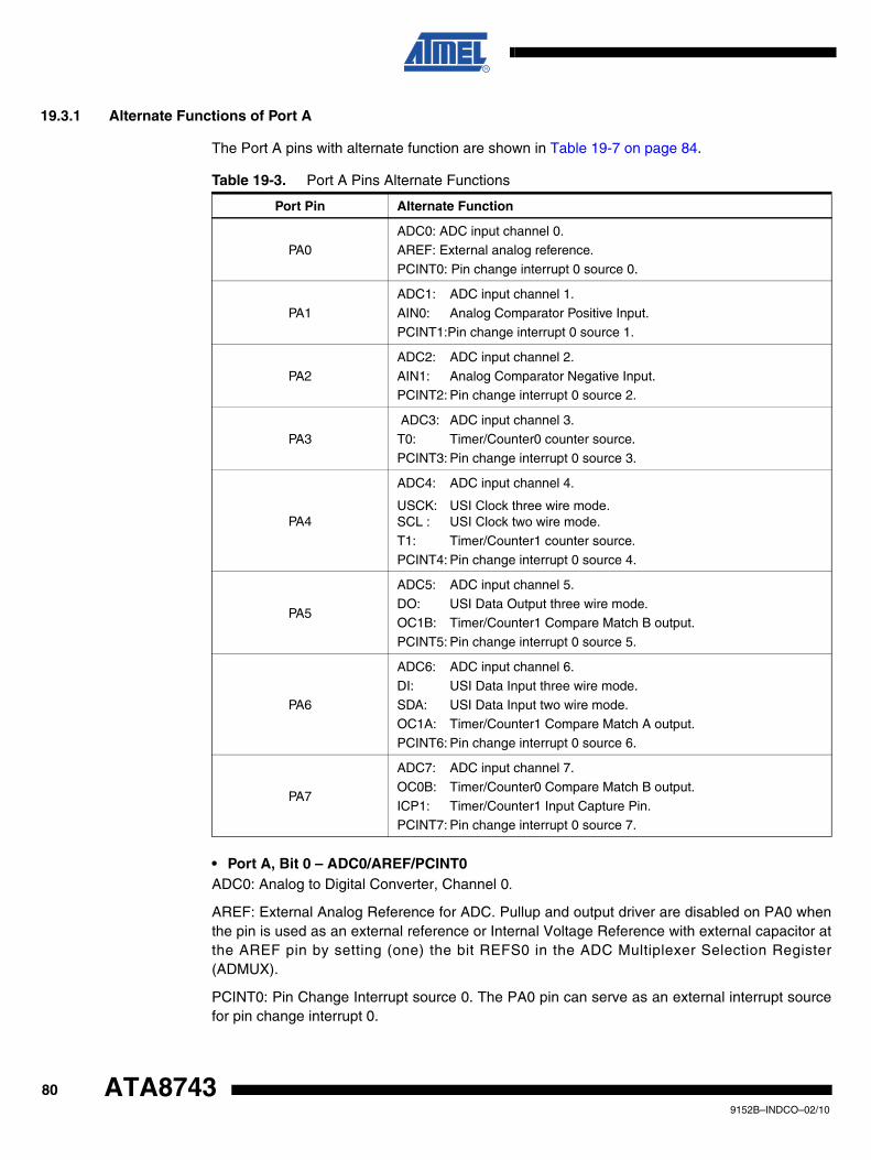
19.3.1 Alternate Functions of Port A
The Port A pins with alternate function are shown in Table 19-7 on page 84.
• Port A, Bit 0 – ADC0/AREF/PCINT0ADC0: Analog to Digital Converter, Channel 0.
AREF: External Analog Reference for ADC. Pullup and output driver are disabled on PA0 whenthe pin is used as an external reference or Internal Voltage Reference with external capacitor atthe AREF pin by setting (one) the bit REFS0 in the ADC Multiplexer Selection Register(ADMUX).
PCINT0: Pin Change Interrupt source 0. The PA0 pin can serve as an external interrupt sourcefor pin change interrupt 0.
Table 19-3. Port A Pins Alternate Functions
Port Pin Alternate Function
PA0ADC0: ADC input channel 0.AREF: External analog reference.
PCINT0: Pin change interrupt 0 source 0.
PA1
ADC1: ADC input channel 1.
AIN0: Analog Comparator Positive Input.
PCINT1:Pin change interrupt 0 source 1.
PA2
ADC2: ADC input channel 2.
AIN1: Analog Comparator Negative Input.PCINT2: Pin change interrupt 0 source 2.
PA3 ADC3: ADC input channel 3.T0: Timer/Counter0 counter source.
PCINT3: Pin change interrupt 0 source 3.
PA4
ADC4: ADC input channel 4.
USCK: USI Clock three wire mode.SCL : USI Clock two wire mode.T1: Timer/Counter1 counter source.
PCINT4: Pin change interrupt 0 source 4.
PA5
ADC5: ADC input channel 5.
DO: USI Data Output three wire mode.OC1B: Timer/Counter1 Compare Match B output.
PCINT5: Pin change interrupt 0 source 5.
PA6
ADC6: ADC input channel 6.
DI: USI Data Input three wire mode.
SDA: USI Data Input two wire mode.OC1A: Timer/Counter1 Compare Match A output.
PCINT6: Pin change interrupt 0 source 6.
PA7
ADC7: ADC input channel 7.
OC0B: Timer/Counter0 Compare Match B output.
ICP1: Timer/Counter1 Input Capture Pin.PCINT7: Pin change interrupt 0 source 7.
809152B–INDCO–02/10
ATA8743
ATA8743
• Port A, Bit 1 – ADC1/AIN0/PCINT1ADC1: Analog to Digital Converter, Channel 1.
AIN0: Analog Comparator Positive Input. Configure the port pin as input with the internal pull-upswitched off to avoid the digital port function from interfering with the function of the AnalogComparator.
PCINT1: Pin Change Interrupt source 1. The PA1 pin can serve as an external interrupt sourcefor pin change interrupt 0.
• Port A, Bit 2 – ADC2/AIN1/PCINT2ADC2: Analog to Digital Converter, Channel 2.
AIN1: Analog Comparator Negative Input. Configure the port pin as input with the internal pull-upswitched off to avoid the digital port function from interfering with the function of the AnalogComparator.
PCINT2: Pin Change Interrupt source 2. The PA2 pin can serve as an external interrupt sourcefor pin change interrupt 0.
• Port A, Bit 3 – ADC3/T0/PCINT3ADC3: Analog to Digital Converter, Channel 3.
T0: Timer/Counter0 counter source.
PCINT3: Pin Change Interrupt source 3. The PA3 pin can serve as an external interrupt sourcefor pin change interrupt 0.
• Port A, Bit 4 – ADC4/USCK/SCL/T1/PCINT4ADC4: Analog to Digital Converter, Channel 4.
USCK: Three-wire mode Universal Serial Interface Clock.
SCL: Two-wire mode Serial Clock for USI Two-wire mode.
T1: Timer/Counter1 counter source.
PCINT4: Pin Change Interrupt source 4. The PA4 pin can serve as an external interrupt sourcefor pin change interrupt 0.
• Port A, Bit 5 – ADC5/DO/OC1B/PCINT5ADC5: Analog to Digital Converter, Channel 5.
DO: Data Output in USI Three-wire mode. Data output (DO) overrides PORTA5 value and it isdriven to the port when the data direction bit DDA5 is set (one). However the PORTA5 bit stillcontrols the pullup, enabling pullup if direction is input and PORTA5 is set(one).
OC1B: Output Compare Match output: The PA5 pin can serve as an external output for theTimer/Counter1 Compare Match B. The PA5 pin has to be configured as an output (DDA5 set(one)) to serve this function. The OC1B pin is also the output pin for the PWM mode timerfunction.
PCINT5: Pin Change Interrupt source 5. The PA5 pin can serve as an external interrupt sourcefor pin change interrupt 0.
819152B–INDCO–02/10
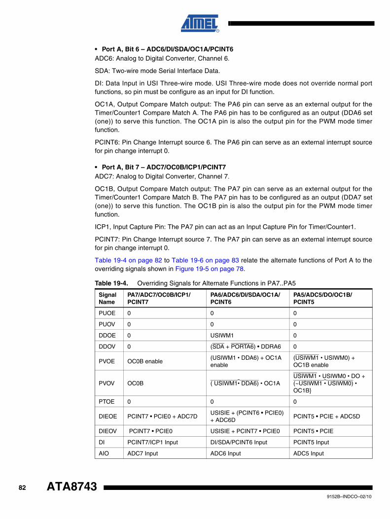
• Port A, Bit 6 – ADC6/DI/SDA/OC1A/PCINT6ADC6: Analog to Digital Converter, Channel 6.
SDA: Two-wire mode Serial Interface Data.
DI: Data Input in USI Three-wire mode. USI Three-wire mode does not override normal portfunctions, so pin must be configure as an input for DI function.
OC1A, Output Compare Match output: The PA6 pin can serve as an external output for theTimer/Counter1 Compare Match A. The PA6 pin has to be configured as an output (DDA6 set(one)) to serve this function. The OC1A pin is also the output pin for the PWM mode timerfunction.
PCINT6: Pin Change Interrupt source 6. The PA6 pin can serve as an external interrupt sourcefor pin change interrupt 0.
• Port A, Bit 7 – ADC7/OC0B/ICP1/PCINT7ADC7: Analog to Digital Converter, Channel 7.
OC1B, Output Compare Match output: The PA7 pin can serve as an external output for theTimer/Counter1 Compare Match B. The PA7 pin has to be configured as an output (DDA7 set(one)) to serve this function. The OC1B pin is also the output pin for the PWM mode timerfunction.
ICP1, Input Capture Pin: The PA7 pin can act as an Input Capture Pin for Timer/Counter1.
PCINT7: Pin Change Interrupt source 7. The PA7 pin can serve as an external interrupt sourcefor pin change interrupt 0.
Table 19-4 on page 82 to Table 19-6 on page 83 relate the alternate functions of Port A to theoverriding signals shown in Figure 19-5 on page 78.
Table 19-4. Overriding Signals for Alternate Functions in PA7..PA5
SignalName
PA7/ADC7/OC0B/ICP1/ PCINT7
PA6/ADC6/DI/SDA/OC1A/ PCINT6
PA5/ADC5/DO/OC1B/ PCINT5
PUOE 0 0 0
PUOV 0 0 0
DDOE 0 USIWM1 0
DDOV 0 (SDA + PORTA6) • DDRA6 0
PVOE OC0B enable(USIWM1 • DDA6) + OC1A enable
(USIWM1 • USIWM0) + OC1B enable
PVOV OC0B ( USIWM1• DDA6) • OC1AUSIWM1 • USIWM0 • DO + (~USIWM1 • USIWM0) • OC1B}
PTOE 0 0 0
DIEOE PCINT7 • PCIE0 + ADC7DUSISIE + (PCINT6 • PCIE0) + ADC6D
PCINT5 • PCIE + ADC5D
DIEOV PCINT7 • PCIE0 USISIE + PCINT7 • PCIE0 PCINT5 • PCIE
DI PCINT7/ICP1 Input DI/SDA/PCINT6 Input PCINT5 Input
AIO ADC7 Input ADC6 Input ADC5 Input
829152B–INDCO–02/10
ATA8743
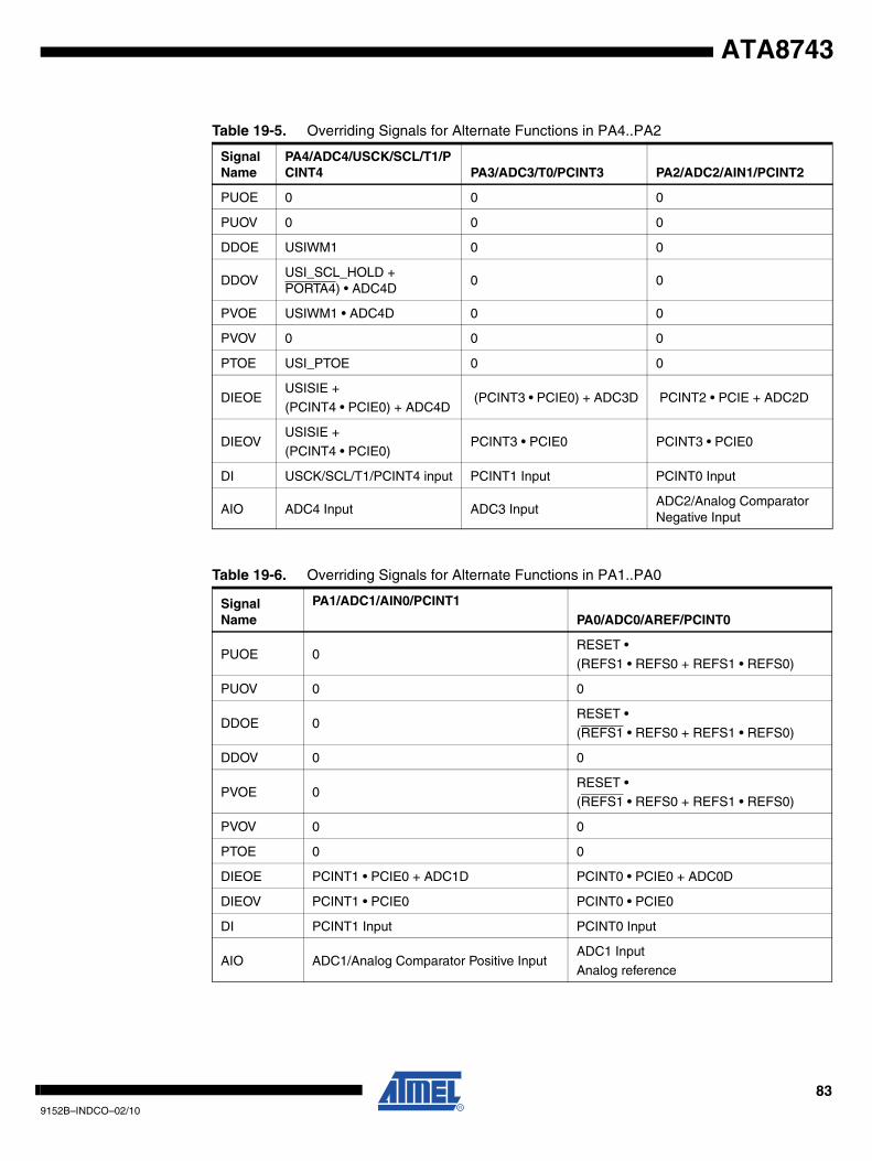
ATA8743
Table 19-5. Overriding Signals for Alternate Functions in PA4..PA2
SignalName
PA4/ADC4/USCK/SCL/T1/PCINT4 PA3/ADC3/T0/PCINT3 PA2/ADC2/AIN1/PCINT2
PUOE 0 0 0
PUOV 0 0 0
DDOE USIWM1 0 0
DDOVUSI_SCL_HOLD + PORTA4) • ADC4D
0 0
PVOE USIWM1 • ADC4D 0 0
PVOV 0 0 0
PTOE USI_PTOE 0 0
DIEOEUSISIE +
(PCINT4 • PCIE0) + ADC4D (PCINT3 • PCIE0) + ADC3D PCINT2 • PCIE + ADC2D
DIEOVUSISIE +
(PCINT4 • PCIE0)PCINT3 • PCIE0 PCINT3 • PCIE0
DI USCK/SCL/T1/PCINT4 input PCINT1 Input PCINT0 Input
AIO ADC4 Input ADC3 InputADC2/Analog Comparator Negative Input
Table 19-6. Overriding Signals for Alternate Functions in PA1..PA0
SignalName
PA1/ADC1/AIN0/PCINT1PA0/ADC0/AREF/PCINT0
PUOE 0RESET •
(REFS1 • REFS0 + REFS1 • REFS0)
PUOV 0 0
DDOE 0RESET •
(REFS1 • REFS0 + REFS1 • REFS0)
DDOV 0 0
PVOE 0RESET • (REFS1 • REFS0 + REFS1 • REFS0)
PVOV 0 0
PTOE 0 0
DIEOE PCINT1 • PCIE0 + ADC1D PCINT0 • PCIE0 + ADC0D
DIEOV PCINT1 • PCIE0 PCINT0 • PCIE0
DI PCINT1 Input PCINT0 Input
AIO ADC1/Analog Comparator Positive InputADC1 Input
Analog reference
839152B–INDCO–02/10
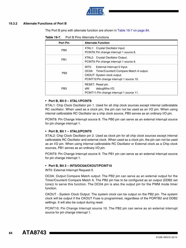
19.3.2 Alternate Functions of Port B
The Port B pins with alternate function are shown in Table 19-7 on page 84.
• Port B, Bit 0 – XTAL1/PCINT8XTAL1: Chip Clock Oscillator pin 1. Used for all chip clock sources except internal calibratableRC oscillator. When used as a clock pin, the pin can not be used as an I/O pin. When usinginternal calibratable RC Oscillator as a chip clock source, PB0 serves as an ordinary I/O pin.
PCINT8: Pin Change Interrupt source 8. The PB0 pin can serve as an external interrupt sourcefor pin change interrupt 1.
• Port B, Bit 1 – XTAL2/PCINT9XTAL2: Chip Clock Oscillator pin 2. Used as clock pin for all chip clock sources except internalcalibratable RC Oscillator and external clock. When used as a clock pin, the pin can not be usedas an I/O pin. When using internal calibratable RC Oscillator or External clock as a Chip clocksources, PB1 serves as an ordinary I/O pin.
PCINT9: Pin Change Interrupt source 9. The PB1 pin can serve as an external interrupt sourcefor pin change interrupt 1.
• Port B, Bit 2 – INT0/OC0A/CKOUT/PCINT10INT0: External Interrupt Request 0.
OC0A: Output Compare Match output: The PB2 pin can serve as an external output for theTimer/Counter0 Compare Match A. The PB2 pin has to be configured as an output (DDB2 set(one)) to serve this function. The OC0A pin is also the output pin for the PWM mode timerfunction.
CKOUT - System Clock Output: The system clock can be output on the PB2 pin. The systemclock will be output if the CKOUT Fuse is programmed, regardless of the PORTB2 and DDB2settings. It will also be output during reset.
PCINT10: Pin Change Interrupt source 10. The PB2 pin can serve as an external interruptsource for pin change interrupt 1.
Table 19-7. Port B Pins Alternate Functions
Port Pin Alternate Function
PB0XTAL1: Crystal Oscillator Input.
PCINT8: Pin change interrupt 1 source 8.
PB1XTAL2: Crystal Oscillator Output.
PCINT9: Pin change interrupt 1 source 9.
PB2
INT0: External Interrupt 0 Input.
OC0A: Timer/Counter0 Compare Match A output.CKOUT: System clock output.
PCINT10:Pin change interrupt 1 source 10.
PB3
RESET: Reset pin.
dW: debugWire I/O.
PCINT11:Pin change interrupt 1 source 11.
849152B–INDCO–02/10
ATA8743
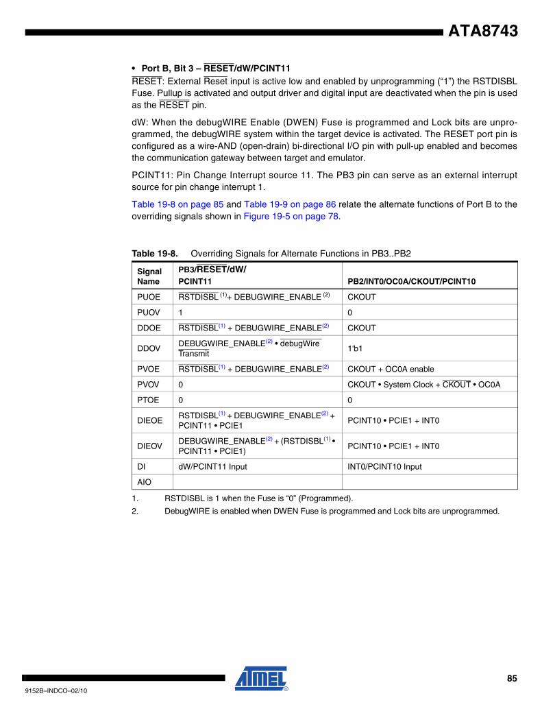
ATA8743
• Port B, Bit 3 – RESET/dW/PCINT11RESET: External Reset input is active low and enabled by unprogramming (“1”) the RSTDISBLFuse. Pullup is activated and output driver and digital input are deactivated when the pin is usedas the RESET pin.
dW: When the debugWIRE Enable (DWEN) Fuse is programmed and Lock bits are unpro-grammed, the debugWIRE system within the target device is activated. The RESET port pin isconfigured as a wire-AND (open-drain) bi-directional I/O pin with pull-up enabled and becomesthe communication gateway between target and emulator.
PCINT11: Pin Change Interrupt source 11. The PB3 pin can serve as an external interruptsource for pin change interrupt 1.
Table 19-8 on page 85 and Table 19-9 on page 86 relate the alternate functions of Port B to theoverriding signals shown in Figure 19-5 on page 78.
Table 19-8. Overriding Signals for Alternate Functions in PB3..PB2
SignalName
PB3/RESET/dW/PCINT11 PB2/INT0/OC0A/CKOUT/PCINT10
PUOE RSTDISBL (1)+ DEBUGWIRE_ENABLE (2)
1. RSTDISBL is 1 when the Fuse is “0” (Programmed).
2. DebugWIRE is enabled when DWEN Fuse is programmed and Lock bits are unprogrammed.
CKOUT
PUOV 1 0
DDOE RSTDISBL(1) + DEBUGWIRE_ENABLE(2) CKOUT
DDOVDEBUGWIRE_ENABLE(2) • debugWire Transmit
1'b1
PVOE RSTDISBL(1) + DEBUGWIRE_ENABLE(2) CKOUT + OC0A enable
PVOV 0 CKOUT • System Clock + CKOUT • OC0A
PTOE 0 0
DIEOERSTDISBL(1) + DEBUGWIRE_ENABLE(2) + PCINT11 • PCIE1
PCINT10 • PCIE1 + INT0
DIEOVDEBUGWIRE_ENABLE(2) + (RSTDISBL(1) • PCINT11 • PCIE1)
PCINT10 • PCIE1 + INT0
DI dW/PCINT11 Input INT0/PCINT10 Input
AIO
859152B–INDCO–02/10
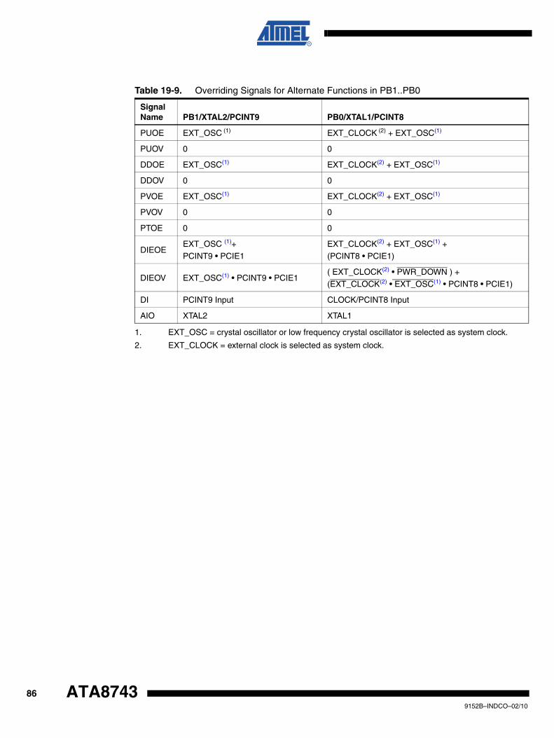
Table 19-9. Overriding Signals for Alternate Functions in PB1..PB0
SignalName PB1/XTAL2/PCINT9 PB0/XTAL1/PCINT8
PUOE EXT_OSC (1)
1. EXT_OSC = crystal oscillator or low frequency crystal oscillator is selected as system clock.
EXT_CLOCK (2) + EXT_OSC(1)
2. EXT_CLOCK = external clock is selected as system clock.
PUOV 0 0
DDOE EXT_OSC(1) EXT_CLOCK(2) + EXT_OSC(1)
DDOV 0 0
PVOE EXT_OSC(1) EXT_CLOCK(2) + EXT_OSC(1)
PVOV 0 0
PTOE 0 0
DIEOEEXT_OSC (1)+
PCINT9 • PCIE1
EXT_CLOCK(2) + EXT_OSC(1) +
(PCINT8 • PCIE1)
DIEOV EXT_OSC(1) • PCINT9 • PCIE1( EXT_CLOCK(2) • PWR_DOWN ) +
(EXT_CLOCK(2) • EXT_OSC(1) • PCINT8 • PCIE1)
DI PCINT9 Input CLOCK/PCINT8 Input
AIO XTAL2 XTAL1
869152B–INDCO–02/10
ATA8743
ATA8743
19.4 Register Description
19.4.1 MCUCR – MCU Control Register
• Bits 7, 2– Res: Reserved BitsThese bits are reserved bits in the ATtiny24/44/84 and will always read as zero.
• Bit 6 – PUD: Pull-up DisableWhen this bit is written to one, the pull-ups in the I/O ports are disabled even if the DDxn andPORTxn Registers are configured to enable the pull-ups ({DDxn, PORTxn} = 0b01). See “Con-figuring the Pin” on page 73 for more details about this feature.
19.4.2 PORTA – Port A Data Register
19.4.3 DDRA – Port A Data Direction Register
19.4.4 PINA – Port A Input Pins Address
19.4.5 PORTB – Port B Data Register
19.4.6 DDRB – Port B Data Direction Register
Bit 7 6 5 4 3 2 1 0
– PUD SE SM1 SM0 – ISC01 ISC00 MCUCR
Read/Write R R/W R/W R/W R/W R R R
Initial Value 0 0 0 0 0 0 0 0
Bit 7 6 5 4 3 2 1 0
0x1B (0x3B) PORTA7 PORTA6 PORTA5 PORTA4 PORTA3 PORTA2 PORTA1 PORTA0 PORTA
Read/Write R/W R/W R/W R/W R/W R/W R/W R/W
Initial Value 0 0 0 0 0 0 0 0
Bit 7 6 5 4 3 2 1 0
0x1A (0x3A) DDA7 DDA6 DDA5 DDA4 DDA3 DDA2 DDA1 DDA0 DDRB
Read/Write R/W R/W R/W R/W R/W R/W R/W R/W
Initial Value 0 0 0 0 0 0 0 0
Bit 7 6 5 4 3 2 1 0
0x19 (0x39) PINA7 PINA6 PINA5 PINA4 PINA3 PINA2 PINA1 PINA0 PINB
Read/Write R/W R/W R/W R/W R/W R/W R/W R/W
Initial Value 0 0 N/A N/A N/A N/A N/A N/A
Bit 7 6 5 4 3 2 1 0
0x18 (0x38) – – PORTB3 PORTB2 PORTB1 PORTB0 PORTB
Read/Write R R R R R/W R/W R/W R/W
Initial Value 0 0 0 0 0 0 0 0
Bit 7 6 5 4 3 2 1 0
0x17 (0x37) – – DDB3 DDB2 DDB1 DDB0 DDRB
Read/Write R R R R R/W R/W R/W R/W
Initial Value 0 0 0 0 0 0 0 0
879152B–INDCO–02/10

19.4.7 PINB – Port BInput Pins Address
Bit 7 6 5 4 3 2 1 0
0x16 (0x36) – – PINB3 PINB2 PINB1 PINB0 PINB
Read/Write R R R R R/W R/W R/W R/W
Initial Value 0 0 N/A N/A N/A N/A N/A N/A
889152B–INDCO–02/10
ATA8743
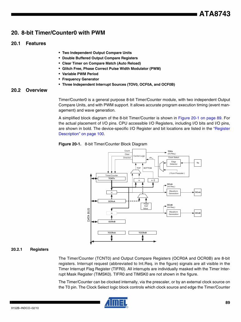
ATA8743
20. 8-bit Timer/Counter0 with PWM
20.1 Features
• Two Independent Output Compare Units• Double Buffered Output Compare Registers• Clear Timer on Compare Match (Auto Reload)• Glitch Free, Phase Correct Pulse Width Modulator (PWM)• Variable PWM Period• Frequency Generator• Three Independent Interrupt Sources (TOV0, OCF0A, and OCF0B)
20.2 Overview
Timer/Counter0 is a general purpose 8-bit Timer/Counter module, with two independent OutputCompare Units, and with PWM support. It allows accurate program execution timing (event man-agement) and wave generation.
A simplified block diagram of the 8-bit Timer/Counter is shown in Figure 20-1 on page 89. Forthe actual placement of I/O pins. CPU accessible I/O Registers, including I/O bits and I/O pins,are shown in bold. The device-specific I/O Register and bit locations are listed in the “RegisterDescription” on page 100.
Figure 20-1. 8-bit Timer/Counter Block Diagram
20.2.1 Registers
The Timer/Counter (TCNT0) and Output Compare Registers (OCR0A and OCR0B) are 8-bitregisters. Interrupt request (abbreviated to Int.Req. in the figure) signals are all visible in theTimer Interrupt Flag Register (TIFR0). All interrupts are individually masked with the Timer Inter-rupt Mask Register (TIMSK0). TIFR0 and TIMSK0 are not shown in the figure.
The Timer/Counter can be clocked internally, via the prescaler, or by an external clock source onthe T0 pin. The Clock Select logic block controls which clock source and edge the Timer/Counter
Clock Select
Timer/Counter
DAT
A B
US
OCRnA
OCRnB
=
=
TCNTn
WaveformGeneration
WaveformGeneration
OCnA
OCnB
=
FixedTOP
Value
Control Logic
= 0
TOP BOTTOM
Count
Clear
Direction
TOVn(Int.Req.)
OCnA(Int.Req.)
OCnB(Int.Req.)
TCCRnA TCCRnB
TnEdge
Detector
( From Prescaler )
clkTn
899152B–INDCO–02/10
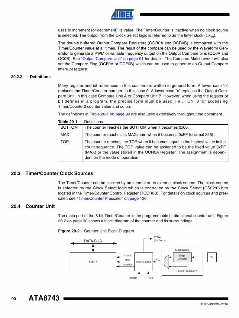
uses to increment (or decrement) its value. The Timer/Counter is inactive when no clock sourceis selected. The output from the Clock Select logic is referred to as the timer clock (clkT0).
The double buffered Output Compare Registers (OCR0A and OCR0B) is compared with theTimer/Counter value at all times. The result of the compare can be used by the Waveform Gen-erator to generate a PWM or variable frequency output on the Output Compare pins (OC0A andOC0B). See “Output Compare Unit” on page 91 for details. The Compare Match event will alsoset the Compare Flag (OCF0A or OCF0B) which can be used to generate an Output Compareinterrupt request.
20.2.2 Definitions
Many register and bit references in this section are written in general form. A lower case “n”replaces the Timer/Counter number, in this case 0. A lower case “x” replaces the Output Com-pare Unit, in this case Compare Unit A or Compare Unit B. However, when using the register orbit defines in a program, the precise form must be used, i.e., TCNT0 for accessingTimer/Counter0 counter value and so on.
The definitions in Table 20-1 on page 90 are also used extensively throughout the document.
Table 20-1. Definitions
20.3 Timer/Counter Clock Sources
The Timer/Counter can be clocked by an internal or an external clock source. The clock sourceis selected by the Clock Select logic which is controlled by the Clock Select (CS02:0) bitslocated in the Timer/Counter Control Register (TCCR0B). For details on clock sources and pres-caler, see “Timer/Counter Prescaler” on page 136.
20.4 Counter Unit
The main part of the 8-bit Timer/Counter is the programmable bi-directional counter unit. Figure20-2 on page 90 shows a block diagram of the counter and its surroundings.
Figure 20-2. Counter Unit Block Diagram
BOTTOM The counter reaches the BOTTOM when it becomes 0x00.
MAX The counter reaches its MAXimum when it becomes 0xFF (decimal 255).
TOP The counter reaches the TOP when it becomes equal to the highest value in thecount sequence. The TOP value can be assigned to be the fixed value 0xFF(MAX) or the value stored in the OCR0A Register. The assignment is depen-dent on the mode of operation.
DATA BUS
TCNTn Control Logic
count
TOVn(Int.Req.)
Clock Select
top
TnEdge
Detector
( From Prescaler )
clkTn
bottom
direction
clear
909152B–INDCO–02/10
ATA8743
ATA8743
Signal description (internal signals):
count Increment or decrement TCNT0 by 1.
direction Select between increment and decrement.
clear Clear TCNT0 (set all bits to zero).
clkTn Timer/Counter clock, referred to as clkT0 in the following.
top Signalize that TCNT0 has reached maximum value.
bottom Signalize that TCNT0 has reached minimum value (zero).
Depending of the mode of operation used, the counter is cleared, incremented, or decrementedat each timer clock (clkT0). clkT0 can be generated from an external or internal clock source,selected by the Clock Select bits (CS02:0). When no clock source is selected (CS02:0 = 0) thetimer is stopped. However, the TCNT0 value can be accessed by the CPU, regardless ofwhether clkT0 is present or not. A CPU write overrides (has priority over) all counter clear orcount operations.
The counting sequence is determined by the setting of the WGM01 and WGM00 bits located inthe Timer/Counter Control Register (TCCR0A) and the WGM02 bit located in the Timer/CounterControl Register B (TCCR0B). There are close connections between how the counter behaves(counts) and how waveforms are generated on the Output Compare output OC0A. For moredetails about advanced counting sequences and waveform generation, see “Modes of Opera-tion” on page 94.
The Timer/Counter Overflow Flag (TOV0) is set according to the mode of operation selected bythe WGM01:0 bits. TOV0 can be used for generating a CPU interrupt.
20.5 Output Compare Unit
The 8-bit comparator continuously compares TCNT0 with the Output Compare Registers(OCR0A and OCR0B). Whenever TCNT0 equals OCR0A or OCR0B, the comparator signals amatch. A match will set the Output Compare Flag (OCF0A or OCF0B) at the next timer clockcycle. If the corresponding interrupt is enabled, the Output Compare Flag generates an OutputCompare interrupt. The Output Compare Flag is automatically cleared when the interrupt is exe-cuted. Alternatively, the flag can be cleared by software by writing a logical one to its I/O bitlocation. The Waveform Generator uses the match signal to generate an output according tooperating mode set by the WGM02:0 bits and Compare Output mode (COM0x1:0) bits. The maxand bottom signals are used by the Waveform Generator for handling the special cases of theextreme values in some modes of operation. See “Modes of Operation” on page 94.
Figure 20-3 on page 92 shows a block diagram of the Output Compare unit.
919152B–INDCO–02/10
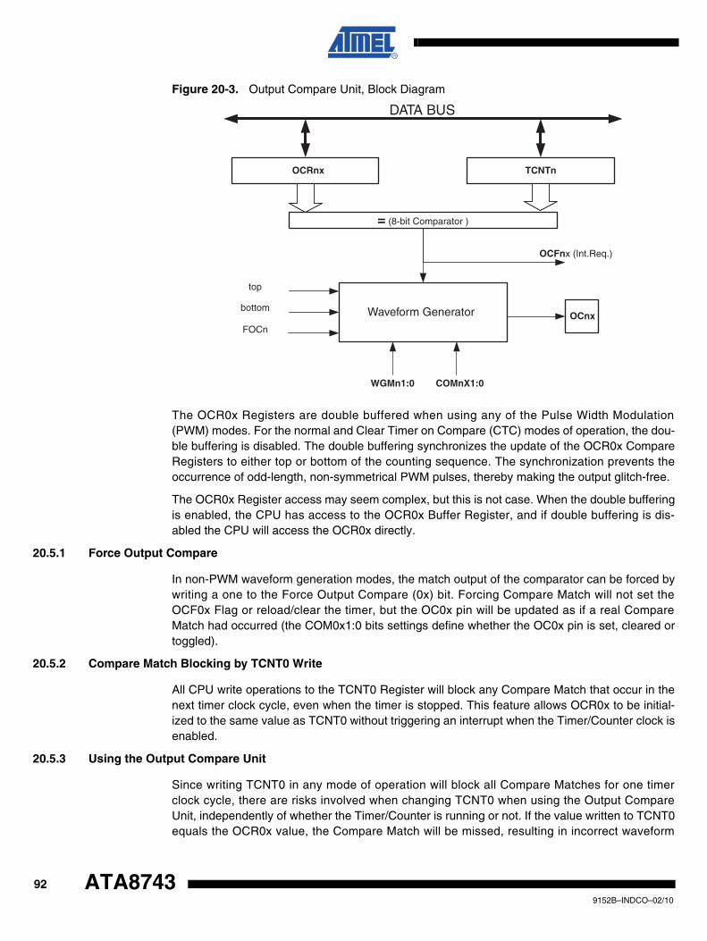
Figure 20-3. Output Compare Unit, Block Diagram
The OCR0x Registers are double buffered when using any of the Pulse Width Modulation(PWM) modes. For the normal and Clear Timer on Compare (CTC) modes of operation, the dou-ble buffering is disabled. The double buffering synchronizes the update of the OCR0x CompareRegisters to either top or bottom of the counting sequence. The synchronization prevents theoccurrence of odd-length, non-symmetrical PWM pulses, thereby making the output glitch-free.
The OCR0x Register access may seem complex, but this is not case. When the double bufferingis enabled, the CPU has access to the OCR0x Buffer Register, and if double buffering is dis-abled the CPU will access the OCR0x directly.
20.5.1 Force Output Compare
In non-PWM waveform generation modes, the match output of the comparator can be forced bywriting a one to the Force Output Compare (0x) bit. Forcing Compare Match will not set theOCF0x Flag or reload/clear the timer, but the OC0x pin will be updated as if a real CompareMatch had occurred (the COM0x1:0 bits settings define whether the OC0x pin is set, cleared ortoggled).
20.5.2 Compare Match Blocking by TCNT0 Write
All CPU write operations to the TCNT0 Register will block any Compare Match that occur in thenext timer clock cycle, even when the timer is stopped. This feature allows OCR0x to be initial-ized to the same value as TCNT0 without triggering an interrupt when the Timer/Counter clock isenabled.
20.5.3 Using the Output Compare Unit
Since writing TCNT0 in any mode of operation will block all Compare Matches for one timerclock cycle, there are risks involved when changing TCNT0 when using the Output CompareUnit, independently of whether the Timer/Counter is running or not. If the value written to TCNT0equals the OCR0x value, the Compare Match will be missed, resulting in incorrect waveform
OCFnx (Int.Req.)
= (8-bit Comparator )
OCRnx
OCnx
DATA BUS
TCNTn
WGMn1:0
Waveform Generator
top
FOCn
COMnX1:0
bottom
929152B–INDCO–02/10
ATA8743
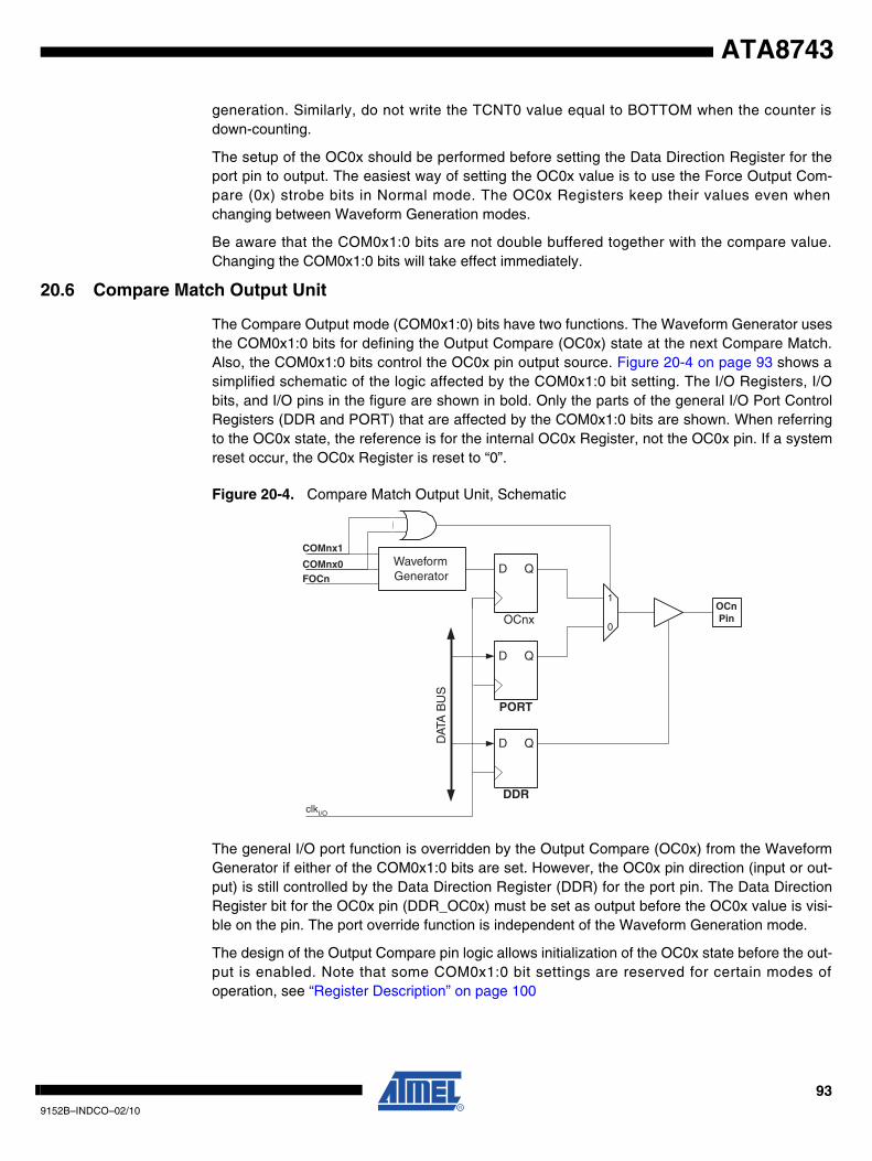
ATA8743
generation. Similarly, do not write the TCNT0 value equal to BOTTOM when the counter isdown-counting.
The setup of the OC0x should be performed before setting the Data Direction Register for theport pin to output. The easiest way of setting the OC0x value is to use the Force Output Com-pare (0x) strobe bits in Normal mode. The OC0x Registers keep their values even whenchanging between Waveform Generation modes.
Be aware that the COM0x1:0 bits are not double buffered together with the compare value.Changing the COM0x1:0 bits will take effect immediately.
20.6 Compare Match Output Unit
The Compare Output mode (COM0x1:0) bits have two functions. The Waveform Generator usesthe COM0x1:0 bits for defining the Output Compare (OC0x) state at the next Compare Match.Also, the COM0x1:0 bits control the OC0x pin output source. Figure 20-4 on page 93 shows asimplified schematic of the logic affected by the COM0x1:0 bit setting. The I/O Registers, I/Obits, and I/O pins in the figure are shown in bold. Only the parts of the general I/O Port ControlRegisters (DDR and PORT) that are affected by the COM0x1:0 bits are shown. When referringto the OC0x state, the reference is for the internal OC0x Register, not the OC0x pin. If a systemreset occur, the OC0x Register is reset to “0”.
Figure 20-4. Compare Match Output Unit, Schematic
The general I/O port function is overridden by the Output Compare (OC0x) from the WaveformGenerator if either of the COM0x1:0 bits are set. However, the OC0x pin direction (input or out-put) is still controlled by the Data Direction Register (DDR) for the port pin. The Data DirectionRegister bit for the OC0x pin (DDR_OC0x) must be set as output before the OC0x value is visi-ble on the pin. The port override function is independent of the Waveform Generation mode.
The design of the Output Compare pin logic allows initialization of the OC0x state before the out-put is enabled. Note that some COM0x1:0 bit settings are reserved for certain modes ofoperation, see “Register Description” on page 100
PORT
DDR
D Q
D Q
OCnPinOCnx
D QWaveformGenerator
COMnx1
COMnx0
0
1
DAT
A B
US
FOCn
clkI/O
939152B–INDCO–02/10
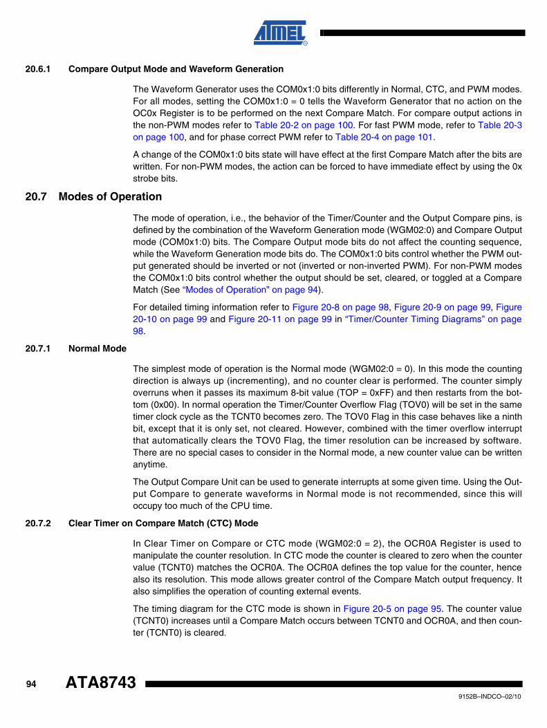
20.6.1 Compare Output Mode and Waveform Generation
The Waveform Generator uses the COM0x1:0 bits differently in Normal, CTC, and PWM modes.For all modes, setting the COM0x1:0 = 0 tells the Waveform Generator that no action on theOC0x Register is to be performed on the next Compare Match. For compare output actions inthe non-PWM modes refer to Table 20-2 on page 100. For fast PWM mode, refer to Table 20-3on page 100, and for phase correct PWM refer to Table 20-4 on page 101.
A change of the COM0x1:0 bits state will have effect at the first Compare Match after the bits arewritten. For non-PWM modes, the action can be forced to have immediate effect by using the 0xstrobe bits.
20.7 Modes of Operation
The mode of operation, i.e., the behavior of the Timer/Counter and the Output Compare pins, isdefined by the combination of the Waveform Generation mode (WGM02:0) and Compare Outputmode (COM0x1:0) bits. The Compare Output mode bits do not affect the counting sequence,while the Waveform Generation mode bits do. The COM0x1:0 bits control whether the PWM out-put generated should be inverted or not (inverted or non-inverted PWM). For non-PWM modesthe COM0x1:0 bits control whether the output should be set, cleared, or toggled at a CompareMatch (See “Modes of Operation” on page 94).
For detailed timing information refer to Figure 20-8 on page 98, Figure 20-9 on page 99, Figure20-10 on page 99 and Figure 20-11 on page 99 in “Timer/Counter Timing Diagrams” on page98.
20.7.1 Normal Mode
The simplest mode of operation is the Normal mode (WGM02:0 = 0). In this mode the countingdirection is always up (incrementing), and no counter clear is performed. The counter simplyoverruns when it passes its maximum 8-bit value (TOP = 0xFF) and then restarts from the bot-tom (0x00). In normal operation the Timer/Counter Overflow Flag (TOV0) will be set in the sametimer clock cycle as the TCNT0 becomes zero. The TOV0 Flag in this case behaves like a ninthbit, except that it is only set, not cleared. However, combined with the timer overflow interruptthat automatically clears the TOV0 Flag, the timer resolution can be increased by software.There are no special cases to consider in the Normal mode, a new counter value can be writtenanytime.
The Output Compare Unit can be used to generate interrupts at some given time. Using the Out-put Compare to generate waveforms in Normal mode is not recommended, since this willoccupy too much of the CPU time.
20.7.2 Clear Timer on Compare Match (CTC) Mode
In Clear Timer on Compare or CTC mode (WGM02:0 = 2), the OCR0A Register is used tomanipulate the counter resolution. In CTC mode the counter is cleared to zero when the countervalue (TCNT0) matches the OCR0A. The OCR0A defines the top value for the counter, hencealso its resolution. This mode allows greater control of the Compare Match output frequency. Italso simplifies the operation of counting external events.
The timing diagram for the CTC mode is shown in Figure 20-5 on page 95. The counter value(TCNT0) increases until a Compare Match occurs between TCNT0 and OCR0A, and then coun-ter (TCNT0) is cleared.
949152B–INDCO–02/10
ATA8743
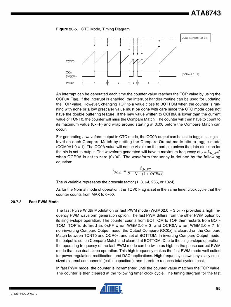
ATA8743
Figure 20-5. CTC Mode, Timing Diagram
An interrupt can be generated each time the counter value reaches the TOP value by using theOCF0A Flag. If the interrupt is enabled, the interrupt handler routine can be used for updatingthe TOP value. However, changing TOP to a value close to BOTTOM when the counter is run-ning with none or a low prescaler value must be done with care since the CTC mode does nothave the double buffering feature. If the new value written to OCR0A is lower than the currentvalue of TCNT0, the counter will miss the Compare Match. The counter will then have to count toits maximum value (0xFF) and wrap around starting at 0x00 before the Compare Match canoccur.
For generating a waveform output in CTC mode, the OC0A output can be set to toggle its logicallevel on each Compare Match by setting the Compare Output mode bits to toggle mode(COM0A1:0 = 1). The OC0A value will not be visible on the port pin unless the data direction forthe pin is set to output. The waveform generated will have a maximum frequency of 0 = fclk_I/O/2when OCR0A is set to zero (0x00). The waveform frequency is defined by the followingequation:
The N variable represents the prescale factor (1, 8, 64, 256, or 1024).
As for the Normal mode of operation, the TOV0 Flag is set in the same timer clock cycle that thecounter counts from MAX to 0x00.
20.7.3 Fast PWM Mode
The fast Pulse Width Modulation or fast PWM mode (WGM02:0 = 3 or 7) provides a high fre-quency PWM waveform generation option. The fast PWM differs from the other PWM option byits single-slope operation. The counter counts from BOTTOM to TOP then restarts from BOT-TOM. TOP is defined as 0xFF when WGM2:0 = 3, and OCR0A when WGM2:0 = 7. Innon-inverting Compare Output mode, the Output Compare (OC0x) is cleared on the CompareMatch between TCNT0 and OCR0x, and set at BOTTOM. In inverting Compare Output mode,the output is set on Compare Match and cleared at BOTTOM. Due to the single-slope operation,the operating frequency of the fast PWM mode can be twice as high as the phase correct PWMmode that use dual-slope operation. This high frequency makes the fast PWM mode well suitedfor power regulation, rectification, and DAC applications. High frequency allows physically smallsized external components (coils, capacitors), and therefore reduces total system cost.
In fast PWM mode, the counter is incremented until the counter value matches the TOP value.The counter is then cleared at the following timer clock cycle. The timing diagram for the fast
TCNTn
OCn(Toggle)
OCnx Interrupt Flag Set
1 4Period 2 3
(COMnx1:0 = 1)
fOCnxfclk_I/O
2 N 1 OCRnx+( )⋅ ⋅-------------------------------------------------------=
959152B–INDCO–02/10
PWM mode is shown in Figure 20-6 on page 96. The TCNT0 value is in the timing diagramshown as a histogram for illustrating the single-slope operation. The diagram includesnon-inverted and inverted PWM outputs. The small horizontal line marks on the TCNT0 slopesrepresent Compare Matches between OCR0x and TCNT0.
Figure 20-6. Fast PWM Mode, Timing Diagram
The Timer/Counter Overflow Flag (TOV0) is set each time the counter reaches TOP. If the inter-rupt is enabled, the interrupt handler routine can be used for updating the compare value.
In fast PWM mode, the compare unit allows generation of PWM waveforms on the OC0x pins.Setting the COM0x1:0 bits to two will produce a non-inverted PWM and an inverted PWM outputcan be generated by setting the COM0x1:0 to three: Setting the COM0A1:0 bits to one allowsthe AC0A pin to toggle on Compare Matches if the WGM02 bit is set. This option is not availablefor the OC0B pin (See Table 20-3 on page 100). The actual OC0x value will only be visible onthe port pin if the data direction for the port pin is set as output. The PWM waveform is gener-ated by setting (or clearing) the OC0x Register at the Compare Match between OCR0x andTCNT0, and clearing (or setting) the OC0x Register at the timer clock cycle the counter iscleared (changes from TOP to BOTTOM).
The PWM frequency for the output can be calculated by the following equation:
The N variable represents the prescale factor (1, 8, 64, 256, or 1024).
The extreme values for the OCR0A Register represents special cases when generating a PWMwaveform output in the fast PWM mode. If the OCR0A is set equal to BOTTOM, the output willbe a narrow spike for each MAX+1 timer clock cycle. Setting the OCR0A equal to MAX will resultin a constantly high or low output (depending on the polarity of the output set by the COM0A1:0bits.)
A frequency (with 50% duty cycle) waveform output in fast PWM mode can be achieved by set-ting OC0x to toggle its logical level on each Compare Match (COM0x1:0 = 1). The waveformgenerated will have a maximum frequency of 0 = fclk_I/O/2 when OCR0A is set to zero. This fea-
TCNTn
OCRnx Update andTOVn Interrupt Flag Set
1Period 2 3
OCn
OCn
(COMnx1:0 = 2)
(COMnx1:0 = 3)
OCRnx Interrupt Flag Set
4 5 6 7
fOCnxPWMfclk_I/O
N 256⋅---------------------=
969152B–INDCO–02/10
ATA8743
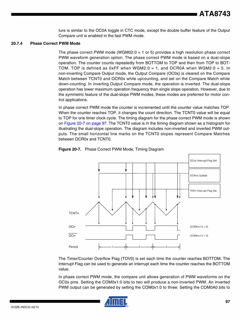
ATA8743
ture is similar to the OC0A toggle in CTC mode, except the double buffer feature of the OutputCompare unit is enabled in the fast PWM mode.
20.7.4 Phase Correct PWM Mode
The phase correct PWM mode (WGM02:0 = 1 or 5) provides a high resolution phase correctPWM waveform generation option. The phase correct PWM mode is based on a dual-slopeoperation. The counter counts repeatedly from BOTTOM to TOP and then from TOP to BOT-TOM. TOP is defined as 0xFF when WGM2:0 = 1, and OCR0A when WGM2:0 = 5. Innon-inverting Compare Output mode, the Output Compare (OC0x) is cleared on the CompareMatch between TCNT0 and OCR0x while upcounting, and set on the Compare Match whiledown-counting. In inverting Output Compare mode, the operation is inverted. The dual-slopeoperation has lower maximum operation frequency than single slope operation. However, due tothe symmetric feature of the dual-slope PWM modes, these modes are preferred for motor con-trol applications.
In phase correct PWM mode the counter is incremented until the counter value matches TOP.When the counter reaches TOP, it changes the count direction. The TCNT0 value will be equalto TOP for one timer clock cycle. The timing diagram for the phase correct PWM mode is shownon Figure 20-7 on page 97. The TCNT0 value is in the timing diagram shown as a histogram forillustrating the dual-slope operation. The diagram includes non-inverted and inverted PWM out-puts. The small horizontal line marks on the TCNT0 slopes represent Compare Matchesbetween OCR0x and TCNT0.
Figure 20-7. Phase Correct PWM Mode, Timing Diagram
The Timer/Counter Overflow Flag (TOV0) is set each time the counter reaches BOTTOM. TheInterrupt Flag can be used to generate an interrupt each time the counter reaches the BOTTOMvalue.
In phase correct PWM mode, the compare unit allows generation of PWM waveforms on theOC0x pins. Setting the COM0x1:0 bits to two will produce a non-inverted PWM. An invertedPWM output can be generated by setting the COM0x1:0 to three: Setting the COM0A0 bits to
TOVn Interrupt Flag Set
OCnx Interrupt Flag Set
1 2 3
TCNTn
Period
OCn
OCn
(COMnx1:0 = 2)
(COMnx1:0 = 3)
OCRnx Update
979152B–INDCO–02/10
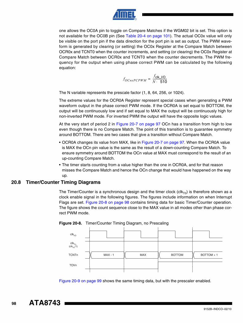
one allows the OC0A pin to toggle on Compare Matches if the WGM02 bit is set. This option isnot available for the OC0B pin (See Table 20-4 on page 101). The actual OC0x value will onlybe visible on the port pin if the data direction for the port pin is set as output. The PWM wave-form is generated by clearing (or setting) the OC0x Register at the Compare Match betweenOCR0x and TCNT0 when the counter increments, and setting (or clearing) the OC0x Register atCompare Match between OCR0x and TCNT0 when the counter decrements. The PWM fre-quency for the output when using phase correct PWM can be calculated by the followingequation:
The N variable represents the prescale factor (1, 8, 64, 256, or 1024).
The extreme values for the OCR0A Register represent special cases when generating a PWMwaveform output in the phase correct PWM mode. If the OCR0A is set equal to BOTTOM, theoutput will be continuously low and if set equal to MAX the output will be continuously high fornon-inverted PWM mode. For inverted PWM the output will have the opposite logic values.
At the very start of period 2 in Figure 20-7 on page 97 OCn has a transition from high to loweven though there is no Compare Match. The point of this transition is to guarantee symmetryaround BOTTOM. There are two cases that give a transition without Compare Match.
• OCR0A changes its value from MAX, like in Figure 20-7 on page 97. When the OCR0A value is MAX the OCn pin value is the same as the result of a down-counting Compare Match. To ensure symmetry around BOTTOM the OCn value at MAX must correspond to the result of an up-counting Compare Match.
• The timer starts counting from a value higher than the one in OCR0A, and for that reason misses the Compare Match and hence the OCn change that would have happened on the way up.
20.8 Timer/Counter Timing Diagrams
The Timer/Counter is a synchronous design and the timer clock (clkT0) is therefore shown as aclock enable signal in the following figures. The figures include information on when InterruptFlags are set. Figure 20-8 on page 98 contains timing data for basic Timer/Counter operation.The figure shows the count sequence close to the MAX value in all modes other than phase cor-rect PWM mode.
Figure 20-8. Timer/Counter Timing Diagram, no Prescaling
Figure 20-9 on page 99 shows the same timing data, but with the prescaler enabled.
fOCnxPCPWMfclk_I/O
N 510⋅---------------------=
clkTn(clkI/O/1)
TOVn
clkI/O
TCNTn MAX - 1 MAX BOTTOM BOTTOM + 1
989152B–INDCO–02/10
ATA8743
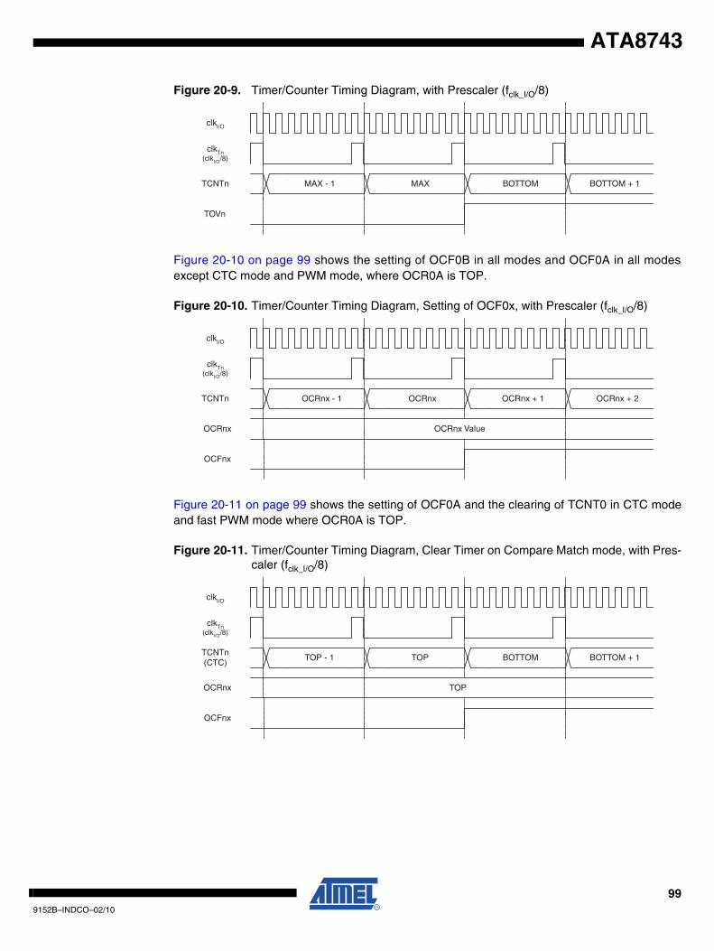
ATA8743
Figure 20-9. Timer/Counter Timing Diagram, with Prescaler (fclk_I/O/8)
Figure 20-10 on page 99 shows the setting of OCF0B in all modes and OCF0A in all modesexcept CTC mode and PWM mode, where OCR0A is TOP.
Figure 20-10. Timer/Counter Timing Diagram, Setting of OCF0x, with Prescaler (fclk_I/O/8)
Figure 20-11 on page 99 shows the setting of OCF0A and the clearing of TCNT0 in CTC modeand fast PWM mode where OCR0A is TOP.
Figure 20-11. Timer/Counter Timing Diagram, Clear Timer on Compare Match mode, with Pres-caler (fclk_I/O/8)
TOVn
TCNTn MAX - 1 MAX BOTTOM BOTTOM + 1
clkI/O
clkTn(clkI/O/8)
OCFnx
OCRnx
TCNTn
OCRnx Value
OCRnx - 1 OCRnx OCRnx + 1 OCRnx + 2
clkI/O
clkTn(clkI/O/8)
OCFnx
OCRnx
TCNTn(CTC)
TOP
TOP - 1 TOP BOTTOM BOTTOM + 1
clkI/O
clkTn(clkI/O/8)
999152B–INDCO–02/10
20.9 Register Description
20.9.1 TCCR0A – Timer/Counter Control Register A
• Bits 7:6 – COM0A1:0: Compare Match Output A ModeThese bits control the Output Compare pin (OC0A) behavior. If one or both of the COM0A1:0bits are set, the OC0A output overrides the normal port functionality of the I/O pin it is connectedto. However, note that the Data Direction Register (DDR) bit corresponding to the OC0A pinmust be set in order to enable the output driver.
When OC0A is connected to the pin, the function of the COM0A1:0 bits depends on theWGM02:0 bit setting. Table 20-2 on page 100 shows the COM0A1:0 bit functionality when theWGM02:0 bits are set to a normal or CTC mode (non-PWM).
Table 20-3 on page 100 shows the COM0A1:0 bit functionality when the WGM01:0 bits are setto fast PWM mode.
Note: 1. A special case occurs when OCR0A equals TOP and COM0A1 is set. In this case, the Com-pare Match is ignored, but the set or clear is done at BOTTOM. See “Fast PWM Mode” on page 95 for more details.
Bit 7 6 5 4 3 2 1 0
0x30 (0x50) COM0A1 COM0A0 COM0B1 COM0B0 – – WGM01 WGM00 TCCR0A
Read/Write R/W R/W R/W R/W R R R/W R/W
Initial Value 0 0 0 0 0 0 0 0
Table 20-2. Compare Output Mode, non-PWM Mode
COM01 COM00 Description
0 0 Normal port operation, OC0A disconnected.
0 1 Toggle OC0A on Compare Match
1 0 Clear OC0A on Compare Match
1 1 Set OC0A on Compare Match
Table 20-3. Compare Output Mode, Fast PWM Mode(1)
COM01 COM00 Description
0 0 Normal port operation, OC0A disconnected.
0 1WGM02 = 0: Normal Port Operation, OC0A Disconnected.WGM02 = 1: Toggle OC0A on Compare Match.
1 0Clear OC0A on Compare Match, set OC0A at BOTTOM(non-inverting mode)
1 1Set OC0A on Compare Match, clear OC0A at BOTTOM(inverting mode)
1009152B–INDCO–02/10
ATA8743
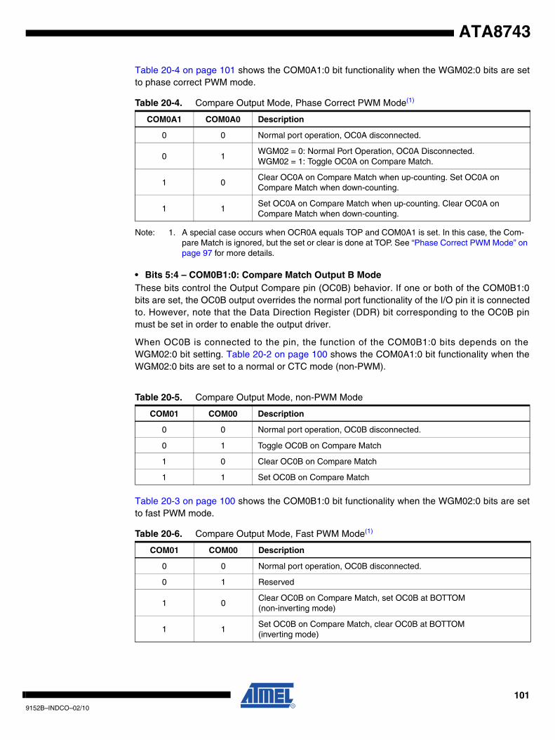
ATA8743
Table 20-4 on page 101 shows the COM0A1:0 bit functionality when the WGM02:0 bits are setto phase correct PWM mode.
Note: 1. A special case occurs when OCR0A equals TOP and COM0A1 is set. In this case, the Com-pare Match is ignored, but the set or clear is done at TOP. See “Phase Correct PWM Mode” on page 97 for more details.
• Bits 5:4 – COM0B1:0: Compare Match Output B ModeThese bits control the Output Compare pin (OC0B) behavior. If one or both of the COM0B1:0bits are set, the OC0B output overrides the normal port functionality of the I/O pin it is connectedto. However, note that the Data Direction Register (DDR) bit corresponding to the OC0B pinmust be set in order to enable the output driver.
When OC0B is connected to the pin, the function of the COM0B1:0 bits depends on theWGM02:0 bit setting. Table 20-2 on page 100 shows the COM0A1:0 bit functionality when theWGM02:0 bits are set to a normal or CTC mode (non-PWM).
Table 20-3 on page 100 shows the COM0B1:0 bit functionality when the WGM02:0 bits are setto fast PWM mode.
Table 20-4. Compare Output Mode, Phase Correct PWM Mode(1)
COM0A1 COM0A0 Description
0 0 Normal port operation, OC0A disconnected.
0 1WGM02 = 0: Normal Port Operation, OC0A Disconnected.WGM02 = 1: Toggle OC0A on Compare Match.
1 0Clear OC0A on Compare Match when up-counting. Set OC0A on Compare Match when down-counting.
1 1Set OC0A on Compare Match when up-counting. Clear OC0A on Compare Match when down-counting.
Table 20-5. Compare Output Mode, non-PWM Mode
COM01 COM00 Description
0 0 Normal port operation, OC0B disconnected.
0 1 Toggle OC0B on Compare Match
1 0 Clear OC0B on Compare Match
1 1 Set OC0B on Compare Match
Table 20-6. Compare Output Mode, Fast PWM Mode(1)
COM01 COM00 Description
0 0 Normal port operation, OC0B disconnected.
0 1 Reserved
1 0Clear OC0B on Compare Match, set OC0B at BOTTOM(non-inverting mode)
1 1Set OC0B on Compare Match, clear OC0B at BOTTOM(inverting mode)
1019152B–INDCO–02/10
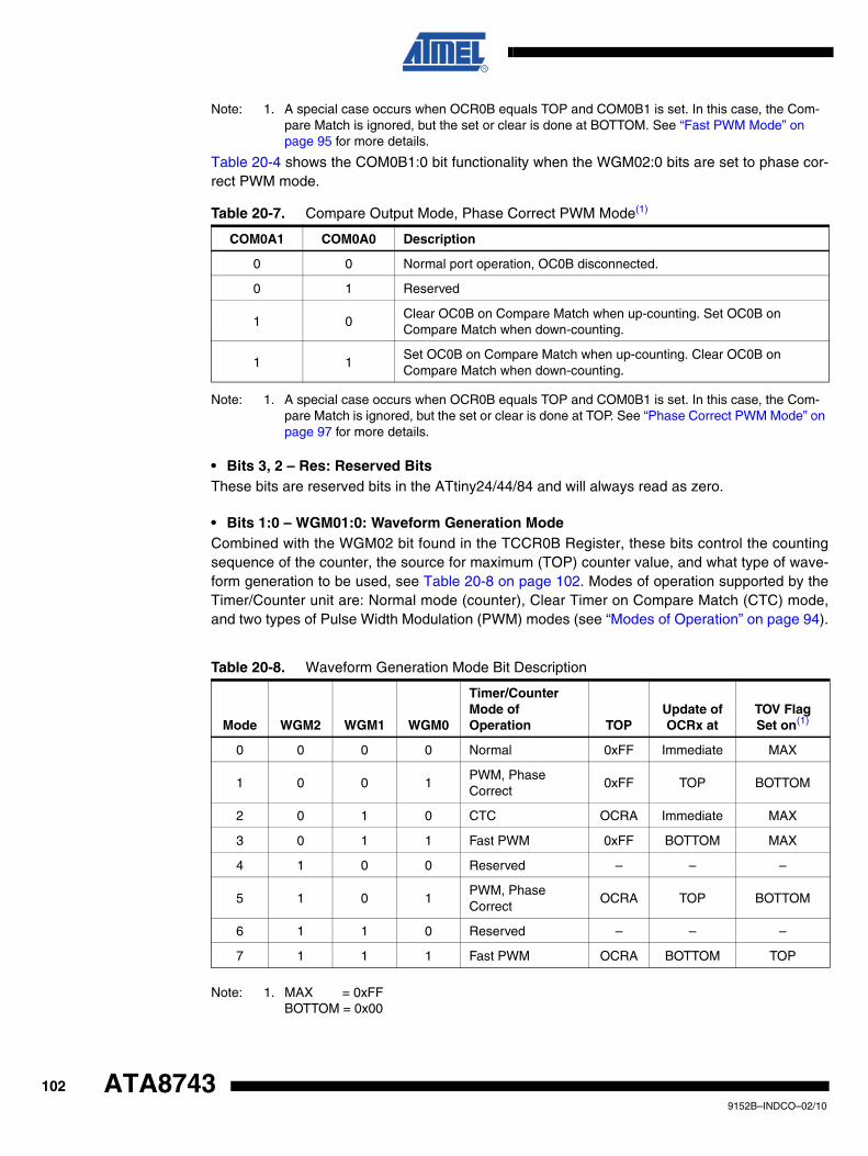
Note: 1. A special case occurs when OCR0B equals TOP and COM0B1 is set. In this case, the Com-pare Match is ignored, but the set or clear is done at BOTTOM. See “Fast PWM Mode” on page 95 for more details.
Table 20-4 shows the COM0B1:0 bit functionality when the WGM02:0 bits are set to phase cor-rect PWM mode.
Note: 1. A special case occurs when OCR0B equals TOP and COM0B1 is set. In this case, the Com-pare Match is ignored, but the set or clear is done at TOP. See “Phase Correct PWM Mode” on page 97 for more details.
• Bits 3, 2 – Res: Reserved BitsThese bits are reserved bits in the ATtiny24/44/84 and will always read as zero.
• Bits 1:0 – WGM01:0: Waveform Generation ModeCombined with the WGM02 bit found in the TCCR0B Register, these bits control the countingsequence of the counter, the source for maximum (TOP) counter value, and what type of wave-form generation to be used, see Table 20-8 on page 102. Modes of operation supported by theTimer/Counter unit are: Normal mode (counter), Clear Timer on Compare Match (CTC) mode,and two types of Pulse Width Modulation (PWM) modes (see “Modes of Operation” on page 94).
Note: 1. MAX = 0xFFBOTTOM = 0x00
Table 20-7. Compare Output Mode, Phase Correct PWM Mode(1)
COM0A1 COM0A0 Description
0 0 Normal port operation, OC0B disconnected.
0 1 Reserved
1 0Clear OC0B on Compare Match when up-counting. Set OC0B on Compare Match when down-counting.
1 1Set OC0B on Compare Match when up-counting. Clear OC0B on Compare Match when down-counting.
Table 20-8. Waveform Generation Mode Bit Description
Mode WGM2 WGM1 WGM0
Timer/Counter Mode of Operation TOP
Update ofOCRx at
TOV FlagSet on(1)
0 0 0 0 Normal 0xFF Immediate MAX
1 0 0 1PWM, Phase Correct
0xFF TOP BOTTOM
2 0 1 0 CTC OCRA Immediate MAX
3 0 1 1 Fast PWM 0xFF BOTTOM MAX
4 1 0 0 Reserved – – –
5 1 0 1PWM, Phase Correct
OCRA TOP BOTTOM
6 1 1 0 Reserved – – –
7 1 1 1 Fast PWM OCRA BOTTOM TOP
1029152B–INDCO–02/10
ATA8743
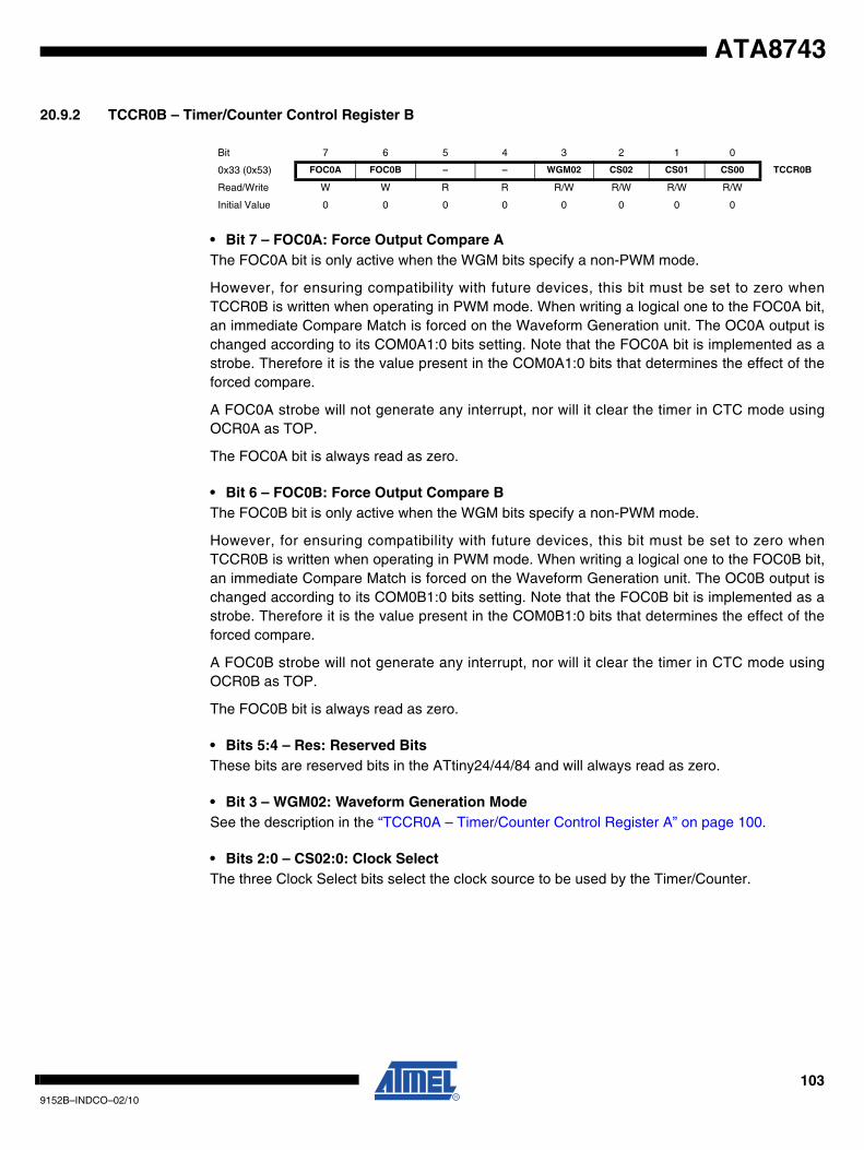
ATA8743
20.9.2 TCCR0B – Timer/Counter Control Register B
• Bit 7 – FOC0A: Force Output Compare AThe FOC0A bit is only active when the WGM bits specify a non-PWM mode.
However, for ensuring compatibility with future devices, this bit must be set to zero whenTCCR0B is written when operating in PWM mode. When writing a logical one to the FOC0A bit,an immediate Compare Match is forced on the Waveform Generation unit. The OC0A output ischanged according to its COM0A1:0 bits setting. Note that the FOC0A bit is implemented as astrobe. Therefore it is the value present in the COM0A1:0 bits that determines the effect of theforced compare.
A FOC0A strobe will not generate any interrupt, nor will it clear the timer in CTC mode usingOCR0A as TOP.
The FOC0A bit is always read as zero.
• Bit 6 – FOC0B: Force Output Compare BThe FOC0B bit is only active when the WGM bits specify a non-PWM mode.
However, for ensuring compatibility with future devices, this bit must be set to zero whenTCCR0B is written when operating in PWM mode. When writing a logical one to the FOC0B bit,an immediate Compare Match is forced on the Waveform Generation unit. The OC0B output ischanged according to its COM0B1:0 bits setting. Note that the FOC0B bit is implemented as astrobe. Therefore it is the value present in the COM0B1:0 bits that determines the effect of theforced compare.
A FOC0B strobe will not generate any interrupt, nor will it clear the timer in CTC mode usingOCR0B as TOP.
The FOC0B bit is always read as zero.
• Bits 5:4 – Res: Reserved BitsThese bits are reserved bits in the ATtiny24/44/84 and will always read as zero.
• Bit 3 – WGM02: Waveform Generation ModeSee the description in the “TCCR0A – Timer/Counter Control Register A” on page 100.
• Bits 2:0 – CS02:0: Clock SelectThe three Clock Select bits select the clock source to be used by the Timer/Counter.
Bit 7 6 5 4 3 2 1 0
0x33 (0x53) FOC0A FOC0B – – WGM02 CS02 CS01 CS00 TCCR0B
Read/Write W W R R R/W R/W R/W R/W
Initial Value 0 0 0 0 0 0 0 0
1039152B–INDCO–02/10
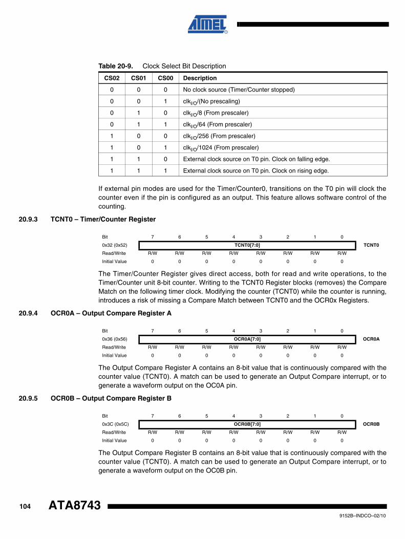
If external pin modes are used for the Timer/Counter0, transitions on the T0 pin will clock thecounter even if the pin is configured as an output. This feature allows software control of thecounting.
20.9.3 TCNT0 – Timer/Counter Register
The Timer/Counter Register gives direct access, both for read and write operations, to theTimer/Counter unit 8-bit counter. Writing to the TCNT0 Register blocks (removes) the CompareMatch on the following timer clock. Modifying the counter (TCNT0) while the counter is running,introduces a risk of missing a Compare Match between TCNT0 and the OCR0x Registers.
20.9.4 OCR0A – Output Compare Register A
The Output Compare Register A contains an 8-bit value that is continuously compared with thecounter value (TCNT0). A match can be used to generate an Output Compare interrupt, or togenerate a waveform output on the OC0A pin.
20.9.5 OCR0B – Output Compare Register B
The Output Compare Register B contains an 8-bit value that is continuously compared with thecounter value (TCNT0). A match can be used to generate an Output Compare interrupt, or togenerate a waveform output on the OC0B pin.
Table 20-9. Clock Select Bit Description
CS02 CS01 CS00 Description
0 0 0 No clock source (Timer/Counter stopped)
0 0 1 clkI/O/(No prescaling)
0 1 0 clkI/O/8 (From prescaler)
0 1 1 clkI/O/64 (From prescaler)
1 0 0 clkI/O/256 (From prescaler)
1 0 1 clkI/O/1024 (From prescaler)
1 1 0 External clock source on T0 pin. Clock on falling edge.
1 1 1 External clock source on T0 pin. Clock on rising edge.
Bit 7 6 5 4 3 2 1 0
0x32 (0x52) TCNT0[7:0] TCNT0
Read/Write R/W R/W R/W R/W R/W R/W R/W R/W
Initial Value 0 0 0 0 0 0 0 0
Bit 7 6 5 4 3 2 1 0
0x36 (0x56) OCR0A[7:0] OCR0A
Read/Write R/W R/W R/W R/W R/W R/W R/W R/W
Initial Value 0 0 0 0 0 0 0 0
Bit 7 6 5 4 3 2 1 0
0x3C (0x5C) OCR0B[7:0] OCR0B
Read/Write R/W R/W R/W R/W R/W R/W R/W R/W
Initial Value 0 0 0 0 0 0 0 0
1049152B–INDCO–02/10
ATA8743
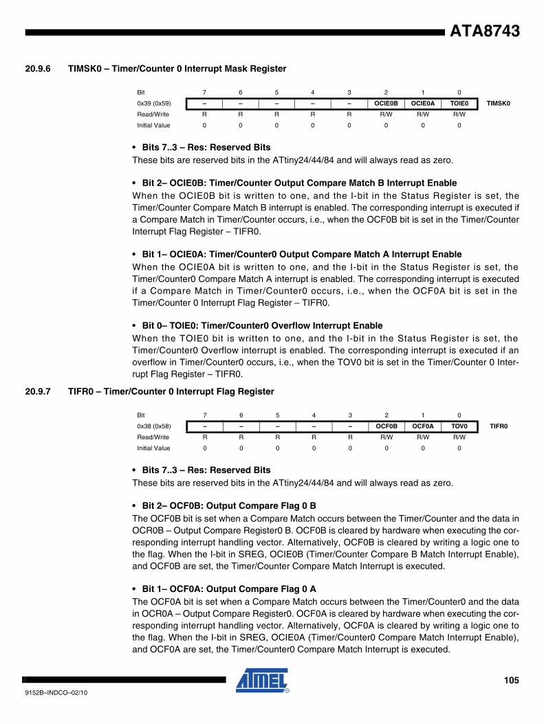
ATA8743
20.9.6 TIMSK0 – Timer/Counter 0 Interrupt Mask Register
• Bits 7..3 – Res: Reserved BitsThese bits are reserved bits in the ATtiny24/44/84 and will always read as zero.
• Bit 2– OCIE0B: Timer/Counter Output Compare Match B Interrupt EnableWhen the OCIE0B bit is written to one, and the I-bit in the Status Register is set, theTimer/Counter Compare Match B interrupt is enabled. The corresponding interrupt is executed ifa Compare Match in Timer/Counter occurs, i.e., when the OCF0B bit is set in the Timer/CounterInterrupt Flag Register – TIFR0.
• Bit 1– OCIE0A: Timer/Counter0 Output Compare Match A Interrupt EnableWhen the OCIE0A bit is written to one, and the I-bit in the Status Register is set, theTimer/Counter0 Compare Match A interrupt is enabled. The corresponding interrupt is executedif a Compare Match in Timer/Counter0 occurs, i.e., when the OCF0A bit is set in theTimer/Counter 0 Interrupt Flag Register – TIFR0.
• Bit 0– TOIE0: Timer/Counter0 Overflow Interrupt EnableWhen the TOIE0 bit is written to one, and the I-bit in the Status Register is set, theTimer/Counter0 Overflow interrupt is enabled. The corresponding interrupt is executed if anoverflow in Timer/Counter0 occurs, i.e., when the TOV0 bit is set in the Timer/Counter 0 Inter-rupt Flag Register – TIFR0.
20.9.7 TIFR0 – Timer/Counter 0 Interrupt Flag Register
• Bits 7..3 – Res: Reserved BitsThese bits are reserved bits in the ATtiny24/44/84 and will always read as zero.
• Bit 2– OCF0B: Output Compare Flag 0 BThe OCF0B bit is set when a Compare Match occurs between the Timer/Counter and the data inOCR0B – Output Compare Register0 B. OCF0B is cleared by hardware when executing the cor-responding interrupt handling vector. Alternatively, OCF0B is cleared by writing a logic one tothe flag. When the I-bit in SREG, OCIE0B (Timer/Counter Compare B Match Interrupt Enable),and OCF0B are set, the Timer/Counter Compare Match Interrupt is executed.
• Bit 1– OCF0A: Output Compare Flag 0 AThe OCF0A bit is set when a Compare Match occurs between the Timer/Counter0 and the datain OCR0A – Output Compare Register0. OCF0A is cleared by hardware when executing the cor-responding interrupt handling vector. Alternatively, OCF0A is cleared by writing a logic one tothe flag. When the I-bit in SREG, OCIE0A (Timer/Counter0 Compare Match Interrupt Enable),and OCF0A are set, the Timer/Counter0 Compare Match Interrupt is executed.
Bit 7 6 5 4 3 2 1 0
0x39 (0x59) – – – – – OCIE0B OCIE0A TOIE0 TIMSK0
Read/Write R R R R R R/W R/W R/W
Initial Value 0 0 0 0 0 0 0 0
Bit 7 6 5 4 3 2 1 0
0x38 (0x58) – – – – – OCF0B OCF0A TOV0 TIFR0
Read/Write R R R R R R/W R/W R/W
Initial Value 0 0 0 0 0 0 0 0
1059152B–INDCO–02/10

• Bit 0– TOV0: Timer/Counter0 Overflow FlagThe bit TOV0 is set when an overflow occurs in Timer/Counter0. TOV0 is cleared by hardwarewhen executing the corresponding interrupt handling vector. Alternatively, TOV0 is cleared bywriting a logic one to the flag. When the SREG I-bit, TOIE0 (Timer/Counter0 Overflow InterruptEnable), and TOV0 are set, the Timer/Counter0 Overflow interrupt is executed.
The setting of this flag is dependent of the WGM02:0 bit setting. See Table 20-8 on page 102and “Waveform Generation Mode Bit Description” on page 102.
1069152B–INDCO–02/10
ATA8743
ATA8743
21. 16-bit Timer/Counter1
21.1 Features
• True 16-bit Design (i.e., Allows 16-bit PWM)• Two independent Output Compare Units• Double Buffered Output Compare Registers• One Input Capture Unit• Input Capture Noise Canceler• Clear Timer on Compare Match (Auto Reload)• Glitch-free, Phase Correct Pulse Width Modulator (PWM)• Variable PWM Period• Frequency Generator• External Event Counter• Four independent interrupt Sources (TOV1, OCF1A, OCF1B, and ICF1)
21.2 Overview
The 16-bit Timer/Counter unit allows accurate program execution timing (event management),wave generation, and signal timing measurement.
Most register and bit references in this section are written in general form. A lower case “n”replaces the Timer/Counter number, and a lower case “x” replaces the Output Compare unitchannel. However, when using the register or bit defines in a program, the precise form must beused, i.e., TCNT1 for accessing Timer/Counter1 counter value and so on.
A simplified block diagram of the 16-bit Timer/Counter is shown in Figure 21-1 on page 108. Forthe actual placement of I/O pins. CPU accessible I/O Registers, including I/O bits and I/O pins,are shown in bold. The device-specific I/O Register and bit locations are listed in the “RegisterDescription” on page 129.
1079152B–INDCO–02/10
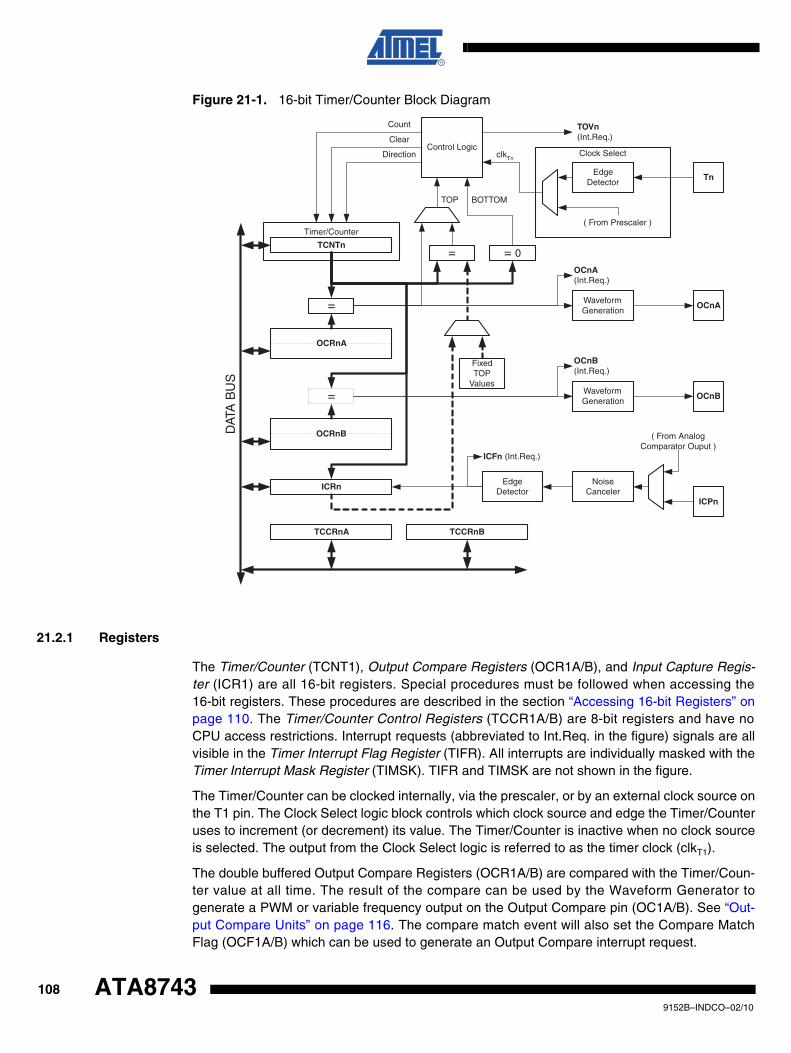
Figure 21-1. 16-bit Timer/Counter Block Diagram
21.2.1 Registers
The Timer/Counter (TCNT1), Output Compare Registers (OCR1A/B), and Input Capture Regis-ter (ICR1) are all 16-bit registers. Special procedures must be followed when accessing the16-bit registers. These procedures are described in the section “Accessing 16-bit Registers” onpage 110. The Timer/Counter Control Registers (TCCR1A/B) are 8-bit registers and have noCPU access restrictions. Interrupt requests (abbreviated to Int.Req. in the figure) signals are allvisible in the Timer Interrupt Flag Register (TIFR). All interrupts are individually masked with theTimer Interrupt Mask Register (TIMSK). TIFR and TIMSK are not shown in the figure.
The Timer/Counter can be clocked internally, via the prescaler, or by an external clock source onthe T1 pin. The Clock Select logic block controls which clock source and edge the Timer/Counteruses to increment (or decrement) its value. The Timer/Counter is inactive when no clock sourceis selected. The output from the Clock Select logic is referred to as the timer clock (clkT1).
The double buffered Output Compare Registers (OCR1A/B) are compared with the Timer/Coun-ter value at all time. The result of the compare can be used by the Waveform Generator togenerate a PWM or variable frequency output on the Output Compare pin (OC1A/B). See “Out-put Compare Units” on page 116. The compare match event will also set the Compare MatchFlag (OCF1A/B) which can be used to generate an Output Compare interrupt request.
Clock Select
Timer/CounterD
ATA
BU
S
OCRnA
OCRnB
ICRn
=
=
TCNTn
WaveformGeneration
WaveformGeneration
OCnA
OCnB
NoiseCanceler
ICPn
=
FixedTOP
Values
EdgeDetector
Control Logic
= 0
TOP BOTTOM
Count
Clear
Direction
TOVn(Int.Req.)
OCnA(Int.Req.)
OCnB(Int.Req.)
ICFn (Int.Req.)
TCCRnA TCCRnB
( From AnalogComparator Ouput )
TnEdge
Detector
( From Prescaler )
clkTn
1089152B–INDCO–02/10
ATA8743
ATA8743
The Input Capture Register can capture the Timer/Counter value at a given external (edge trig-gered) event on either the Input Capture pin (ICP1) or on the Analog Comparator pins (See“Analog Comparator” on page 150). The Input Capture unit includes a digital filtering unit (NoiseCanceler) for reducing the chance of capturing noise spikes.
The TOP value, or maximum Timer/Counter value, can in some modes of operation be definedby either the OCR1A Register, the ICR1 Register, or by a set of fixed values. When usingOCR1A as TOP value in a PWM mode, the OCR1A Register can not be used for generating aPWM output. However, the TOP value will in this case be double buffered allowing the TOPvalue to be changed in run time. If a fixed TOP value is required, the ICR1 Register can be usedas an alternative, freeing the OCR1A to be used as PWM output.
21.2.2 Definitions
The following definitions are used extensively throughout the section:
21.2.3 Compatibility
The 16-bit Timer/Counter has been updated and improved from previous versions of the 16-bitAVR Timer/Counter. This 16-bit Timer/Counter is fully compatible with the earlier versionregarding:
• All 16-bit Timer/Counter related I/O Register address locations, including Timer Interrupt Registers.
• Bit locations inside all 16-bit Timer/Counter Registers, including Timer Interrupt Registers.
• Interrupt Vectors.
The following control bits have changed name, but have same functionality and register location:
• PWM10 is changed to WGM10.
• PWM11 is changed to WGM11.
• CTC1 is changed to WGM12.
The following bits are added to the 16-bit Timer/Counter Control Registers:
• 1A and 1B are added to TCCR1A.
• WGM13 is added to TCCR1B.
The 16-bit Timer/Counter has improvements that will affect the compatibility in some specialcases.
BOTTOM The counter reaches the BOTTOM when it becomes 0x0000.
MAX The counter reaches its MAXimum when it becomes 0xFFFF (decimal 65535).
TOP
The counter reaches the TOP when it becomes equal to the highest value in the count sequence. The TOP value can be assigned to be one of the fixed values: 0x00FF, 0x01FF, or 0x03FF, or to the value stored in the OCR1A or ICR1 Register. The assignment is dependent of the mode of operation.
1099152B–INDCO–02/10
21.3 Accessing 16-bit Registers
The TCNT1, OCR1A/B, and ICR1 are 16-bit registers that can be accessed by the AVR CPU viathe 8-bit data bus. The 16-bit register must be byte accessed using two read or write operations.Each 16-bit timer has a single 8-bit register for temporary storing of the high byte of the 16-bitaccess. The same temporary register is shared between all 16-bit registers within each 16-bittimer. Accessing the low byte triggers the 16-bit read or write operation. When the low byte of a16-bit register is written by the CPU, the high byte stored in the temporary register, and the lowbyte written are both copied into the 16-bit register in the same clock cycle. When the low byte ofa 16-bit register is read by the CPU, the high byte of the 16-bit register is copied into the tempo-rary register in the same clock cycle as the low byte is read.
Not all 16-bit accesses uses the temporary register for the high byte. Reading the OCR1A/B16-bit registers does not involve using the temporary register.
To do a 16-bit write, the high byte must be written before the low byte. For a 16-bit read, the lowbyte must be read before the high byte.
The following code examples show how to access the 16-bit timer registers assuming that nointerrupts updates the temporary register. The same principle can be used directly for accessingthe OCR1A/B and ICR1 Registers. Note that when using “C”, the compiler handles the 16-bitaccess.
Note: 1. See “About Code Examples” on page 22.
The assembly code example returns the TCNT1 value in the r17:r16 register pair.
It is important to notice that accessing 16-bit registers are atomic operations. If an interruptoccurs between the two instructions accessing the 16-bit register, and the interrupt codeupdates the temporary register by accessing the same or any other of the 16-bit timer registers,then the result of the access outside the interrupt will be corrupted. Therefore, when both the
Assembly Code Examples(1)
...
; Set TCNT1 to 0x01FFldi r17,0x01
ldi r16,0xFF
out TCNT1H,r17out TCNT1L,r16; Read TCNT1 into r17:r16in r16,TCNT1Lin r17,TCNT1H...
C Code Examples(1)
unsigned int i;
...
/* Set TCNT1 to 0x01FF */TCNT1 = 0x1FF;/* Read TCNT1 into i */i = TCNT1;...
1109152B–INDCO–02/10
ATA8743
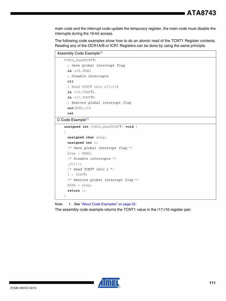
ATA8743
main code and the interrupt code update the temporary register, the main code must disable theinterrupts during the 16-bit access.
The following code examples show how to do an atomic read of the TCNT1 Register contents.Reading any of the OCR1A/B or ICR1 Registers can be done by using the same principle.
Note: 1. See “About Code Examples” on page 22.
The assembly code example returns the TCNT1 value in the r17:r16 register pair.
Assembly Code Example(1)
TIM16_ReadTCNT1:; Save global interrupt flag
in r18,SREG
; Disable interrupts
cli
; Read TCNT1 into r17:r16in r16,TCNT1Lin r17,TCNT1H; Restore global interrupt flag
out SREG,r18
ret
C Code Example(1)
unsigned int TIM16_ReadTCNT1( void ){
unsigned char sreg;
unsigned int i;
/* Save global interrupt flag */
sreg = SREG;
/* Disable interrupts */
_CLI();
/* Read TCNT1 into i */i = TCNT1;/* Restore global interrupt flag */
SREG = sreg;
return i;
}
1119152B–INDCO–02/10
The following code examples show how to do an atomic write of the TCNT1 Register contents.Writing any of the OCR1A/B or ICR1 Registers can be done by using the same principle.
Note: 1. See “About Code Examples” on page 22.
The assembly code example requires that the r17:r16 register pair contains the value to be writ-ten to TCNT1.
21.3.1 Reusing the Temporary High Byte Register
If writing to more than one 16-bit register where the high byte is the same for all registers written,then the high byte only needs to be written once. However, note that the same rule of atomicoperation described previously also applies in this case.
21.4 Timer/Counter Clock Sources
The Timer/Counter can be clocked by an internal or an external clock source. The clock sourceis selected by the Clock Select logic which is controlled by the Clock Select (CS12:0) bitslocated in the Timer/Counter control Register B (TCCR1B). For details on clock sources andprescaler, see “Timer/Counter Prescaler” on page 136.
Assembly Code Example(1)
TIM16_WriteTCNT1:; Save global interrupt flag
in r18,SREG
; Disable interrupts
cli
; Set TCNT1 to r17:r16out TCNT1H,r17out TCNT1L,r16; Restore global interrupt flag
out SREG,r18
ret
C Code Example(1)
void TIM16_WriteTCNT1( unsigned int i ){
unsigned char sreg;
unsigned int i;
/* Save global interrupt flag */
sreg = SREG;
/* Disable interrupts */
_CLI();
/* Set TCNT1 to i */TCNT1 = i;/* Restore global interrupt flag */
SREG = sreg;
}
1129152B–INDCO–02/10
ATA8743
ATA8743
21.5 Counter Unit
The main part of the 16-bit Timer/Counter is the programmable 16-bit bi-directional counter unit.Figure 21-2 on page 113 shows a block diagram of the counter and its surroundings.
Figure 21-2. Counter Unit Block Diagram
Signal description (internal signals):
Count Increment or decrement TCNT1 by 1.
Direction Select between increment and decrement.
Clear Clear TCNT1 (set all bits to zero).
clkT1 Timer/Counter clock.
TOP Signalize that TCNT1 has reached maximum value.
BOTTOM Signalize that TCNT1 has reached minimum value (zero).
The 16-bit counter is mapped into two 8-bit I/O memory locations: Counter High (TCNT1H) con-taining the upper eight bits of the counter, and Counter Low (TCNT1L) containing the lower eightbits. The TCNT1H Register can only be indirectly accessed by the CPU. When the CPU does anaccess to the TCNT1H I/O location, the CPU accesses the high byte temporary register (TEMP).The temporary register is updated with the TCNT1H value when the TCNT1L is read, andTCNT1H is updated with the temporary register value when TCNT1L is written. This allows theCPU to read or write the entire 16-bit counter value within one clock cycle via the 8-bit data bus.It is important to notice that there are special cases of writing to the TCNT1 Register when thecounter is counting that will give unpredictable results. The special cases are described in thesections where they are of importance.
Depending on the mode of operation used, the counter is cleared, incremented, or decrementedat each timer clock (clkT1). The clkT1 can be generated from an external or internal clock source,selected by the Clock Select bits (CS12:0). When no clock source is selected (CS12:0 = 0) thetimer is stopped. However, the TCNT1 value can be accessed by the CPU, independent ofwhether clkT1 is present or not. A CPU write overrides (has priority over) all counter clear orcount operations.
The counting sequence is determined by the setting of the Waveform Generation mode bits(WGM13:0) located in the Timer/Counter Control Registers A and B (TCCR1A and TCCR1B).There are close connections between how the counter behaves (counts) and how waveformsare generated on the Output Compare outputs OC1x. For more details about advanced countingsequences and waveform generation, see “Modes of Operation” on page 119.
TEMP (8-bit)
DATA BUS (8-bit)
TCNTn (16-bit Counter)
TCNTnH (8-bit) TCNTnL (8-bit)Control Logic
Count
Clear
Direction
TOVn(Int.Req.)
Clock Select
TOP BOTTOM
TnEdge
Detector
( From Prescaler )
clkTn
1139152B–INDCO–02/10
The Timer/Counter Overflow Flag (TOV1) is set according to the mode of operation selected bythe WGM13:0 bits. TOV1 can be used for generating a CPU interrupt.
21.6 Input Capture Unit
The Timer/Counter incorporates an Input Capture unit that can capture external events and givethem a time-stamp indicating time of occurrence. The external signal indicating an event, or mul-tiple events, can be applied via the ICP1 pin or alternatively, via the analog-comparator unit. Thetime-stamps can then be used to calculate frequency, duty-cycle, and other features of the sig-nal applied. Alternatively the time-stamps can be used for creating a log of the events.
The Input Capture unit is illustrated by the block diagram shown in Figure 21-3 on page 114. Theelements of the block diagram that are not directly a part of the Input Capture unit are grayshaded. The small “n” in register and bit names indicates the Timer/Counter number.
Figure 21-3. Input Capture Unit Block Diagram
When a change of the logic level (an event) occurs on the Input Capture pin (ICP1), alternativelyon the Analog Comparator output (ACO), and this change confirms to the setting of the edgedetector, a capture will be triggered. When a capture is triggered, the 16-bit value of the counter(TCNT1) is written to the Input Capture Register (ICR1). The Input Capture Flag (ICF1) is set atthe same system clock as the TCNT1 value is copied into ICR1 Register. If enabled (ICIE1 = 1),the Input Capture Flag generates an Input Capture interrupt. The ICF1 flag is automaticallycleared when the interrupt is executed. Alternatively the ICF1 flag can be cleared by software bywriting a logical one to its I/O bit location.
Reading the 16-bit value in the Input Capture Register (ICR1) is done by first reading the lowbyte (ICR1L) and then the high byte (ICR1H). When the low byte is read the high byte is copiedinto the high byte temporary register (TEMP). When the CPU reads the ICR1H I/O location it willaccess the TEMP Register.
The ICR1 Register can only be written when using a Waveform Generation mode that utilizesthe ICR1 Register for defining the counter’s TOP value. In these cases the Waveform Genera-
ICFn (Int.Req.)
AnalogComparator
WRITE ICRn (16-bit Register)
ICRnH (8-bit)
NoiseCanceler
ICPn
EdgeDetector
TEMP (8-bit)
DATA BUS (8-bit)
ICRnL (8-bit)
TCNTn (16-bit Counter)
TCNTnH (8-bit) TCNTnL (8-bit)
ACIC* ICNC ICESACO*
1149152B–INDCO–02/10
ATA8743
ATA8743
tion mode (WGM13:0) bits must be set before the TOP value can be written to the ICR1Register. When writing the ICR1 Register the high byte must be written to the ICR1H I/O locationbefore the low byte is written to ICR1L.
For more information on how to access the 16-bit registers refer to “Accessing 16-bit Registers”on page 110.
21.6.1 Input Capture Trigger Source
The main trigger source for the Input Capture unit is the Input Capture pin (ICP1).Timer/Counter1 can alternatively use the Analog Comparator output as trigger source for theInput Capture unit. The Analog Comparator is selected as trigger source by setting the AnalogComparator Input Capture (ACIC) bit in the Analog Comparator Control and Status Register(ACSR). Be aware that changing trigger source can trigger a capture. The Input Capture Flagmust therefore be cleared after the change.
Both the Input Capture pin (ICP1) and the Analog Comparator output (ACO) inputs are sampledusing the same technique as for the T1 pin (Figure 22-1 on page 136). The edge detector is alsoidentical. However, when the noise canceler is enabled, additional logic is inserted before theedge detector, which increases the delay by four system clock cycles. Note that the input of thenoise canceler and edge detector is always enabled unless the Timer/Counter is set in a Wave-form Generation mode that uses ICR1 to define TOP.
An Input Capture can be triggered by software by controlling the port of the ICP1 pin.
21.6.2 Noise Canceler
The noise canceler improves noise immunity by using a simple digital filtering scheme. Thenoise canceler input is monitored over four samples, and all four must be equal for changing theoutput that in turn is used by the edge detector.
The noise canceler is enabled by setting the Input Capture Noise Canceler (ICNC1) bit inTimer/Counter Control Register B (TCCR1B). When enabled the noise canceler introduces addi-tional four system clock cycles of delay from a change applied to the input, to the update of theICR1 Register. The noise canceler uses the system clock and is therefore not affected by theprescaler.
21.6.3 Using the Input Capture Unit
The main challenge when using the Input Capture unit is to assign enough processor capacityfor handling the incoming events. The time between two events is critical. If the processor hasnot read the captured value in the ICR1 Register before the next event occurs, the ICR1 will beoverwritten with a new value. In this case the result of the capture will be incorrect.
When using the Input Capture interrupt, the ICR1 Register should be read as early in the inter-rupt handler routine as possible. Even though the Input Capture interrupt has relatively highpriority, the maximum interrupt response time is dependent on the maximum number of clockcycles it takes to handle any of the other interrupt requests.
Using the Input Capture unit in any mode of operation when the TOP value (resolution) isactively changed during operation, is not recommended.
Measurement of an external signal’s duty cycle requires that the trigger edge is changed aftereach capture. Changing the edge sensing must be done as early as possible after the ICR1Register has been read. After a change of the edge, the Input Capture Flag (ICF1) must be
1159152B–INDCO–02/10
cleared by software (writing a logical one to the I/O bit location). For measuring frequency only,the clearing of the ICF1 flag is not required (if an interrupt handler is used).
21.7 Output Compare Units
The 16-bit comparator continuously compares TCNT1 with the Output Compare Register(OCR1x). If TCNT equals OCR1x the comparator signals a match. A match will set the OutputCompare Flag (OCF1x) at the next timer clock cycle. If enabled (OCIE1x = 1), the Output Com-pare Flag generates an Output Compare interrupt. The OCF1x flag is automatically clearedwhen the interrupt is executed. Alternatively the OCF1x flag can be cleared by software by writ-ing a logical one to its I/O bit location. The Waveform Generator uses the match signal togenerate an output according to operating mode set by the Waveform Generation mode(WGM13:0) bits and Compare Output mode (COM1x1:0) bits. The TOP and BOTTOM signalsare used by the Waveform Generator for handling the special cases of the extreme values insome modes of operation (“Modes of Operation” on page 119).
A special feature of Output Compare unit A allows it to define the Timer/Counter TOP value (i.e.,counter resolution). In addition to the counter resolution, the TOP value defines the period timefor waveforms generated by the Waveform Generator.
Figure 21-4 on page 116 shows a block diagram of the Output Compare unit. The small “n” inthe register and bit names indicates the device number (n = 1 for Timer/Counter 1), and the “x”indicates Output Compare unit (A/B). The elements of the block diagram that are not directly apart of the Output Compare unit are gray shaded.
Figure 21-4. Output Compare Unit, Block Diagram
The OCR1x Register is double buffered when using any of the twelve Pulse Width Modulation(PWM) modes. For the Normal and Clear Timer on Compare (CTC) modes of operation, thedouble buffering is disabled. The double buffering synchronizes the update of the OCR1x Com-pare Register to either TOP or BOTTOM of the counting sequence. The synchronization
OCFnx (Int.Req.)
= (16-bit Comparator )
OCRnx Buffer (16-bit Register)
OCRnxH Buf. (8-bit)
OCnx
TEMP (8-bit)
DATA BUS (8-bit)
OCRnxL Buf. (8-bit)
TCNTn (16-bit Counter)
TCNTnH (8-bit) TCNTnL (8-bit)
COMnx1:0WGMn3:0
OCRnx (16-bit Register)
OCRnxH (8-bit) OCRnxL (8-bit)
Waveform GeneratorTOP
BOTTOM
1169152B–INDCO–02/10
ATA8743
ATA8743
prevents the occurrence of odd-length, non-symmetrical PWM pulses, thereby making the out-put glitch-free.
The OCR1x Register access may seem complex, but this is not case. When the double bufferingis enabled, the CPU has access to the OCR1x Buffer Register, and if double buffering is dis-abled the CPU will access the OCR1x directly. The content of the OCR1x (Buffer or Compare)Register is only changed by a write operation (the Timer/Counter does not update this registerautomatically as the TCNT1 and ICR1 Register). Therefore OCR1x is not read via the high bytetemporary register (TEMP). However, it is a good practice to read the low byte first as whenaccessing other 16-bit registers. Writing the OCR1x Registers must be done via the TEMP Reg-ister since the compare of all 16 bits is done continuously. The high byte (OCR1xH) has to bewritten first. When the high byte I/O location is written by the CPU, the TEMP Register will beupdated by the value written. Then when the low byte (OCR1xL) is written to the lower eight bits,the high byte will be copied into the upper 8-bits of either the OCR1x buffer or OCR1x CompareRegister in the same system clock cycle.
For more information of how to access the 16-bit registers refer to “Accessing 16-bit Registers”on page 110.
21.7.1 Force Output Compare
In non-PWM Waveform Generation modes, the match output of the comparator can be forced bywriting a one to the Force Output Compare (1x) bit. Forcing compare match will not set theOCF1x flag or reload/clear the timer, but the OC1x pin will be updated as if a real comparematch had occurred (the COM11:0 bits settings define whether the OC1x pin is set, cleared ortoggled).
21.7.2 Compare Match Blocking by TCNT1 Write
All CPU writes to the TCNT1 Register will block any compare match that occurs in the next timerclock cycle, even when the timer is stopped. This feature allows OCR1x to be initialized to thesame value as TCNT1 without triggering an interrupt when the Timer/Counter clock is enabled.
21.7.3 Using the Output Compare Unit
Since writing TCNT1 in any mode of operation will block all compare matches for one timer clockcycle, there are risks involved when changing TCNT1 when using any of the Output Comparechannels, independent of whether the Timer/Counter is running or not. If the value written toTCNT1 equals the OCR1x value, the compare match will be missed, resulting in incorrect wave-form generation. Do not write the TCNT1 equal to TOP in PWM modes with variable TOPvalues. The compare match for the TOP will be ignored and the counter will continue to 0xFFFF.Similarly, do not write the TCNT1 value equal to BOTTOM when the counter is downcounting.
The setup of the OC1x should be performed before setting the Data Direction Register for theport pin to output. The easiest way of setting the OC1x value is to use the Force Output Com-pare (1x) strobe bits in Normal mode. The OC1x Register keeps its value even when changingbetween Waveform Generation modes.
Be aware that the COM1x1:0 bits are not double buffered together with the compare value.Changing the COM1x1:0 bits will take effect immediately.
1179152B–INDCO–02/10
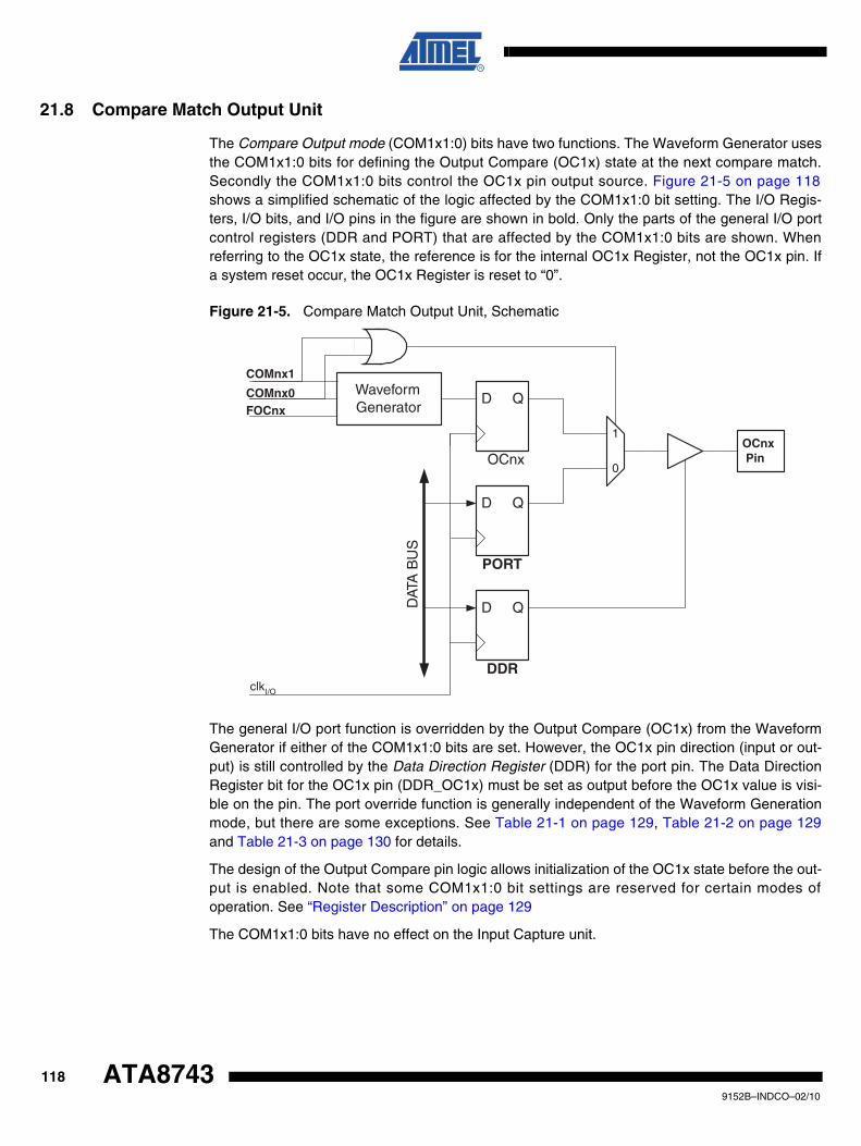
21.8 Compare Match Output Unit
The Compare Output mode (COM1x1:0) bits have two functions. The Waveform Generator usesthe COM1x1:0 bits for defining the Output Compare (OC1x) state at the next compare match.Secondly the COM1x1:0 bits control the OC1x pin output source. Figure 21-5 on page 118shows a simplified schematic of the logic affected by the COM1x1:0 bit setting. The I/O Regis-ters, I/O bits, and I/O pins in the figure are shown in bold. Only the parts of the general I/O portcontrol registers (DDR and PORT) that are affected by the COM1x1:0 bits are shown. Whenreferring to the OC1x state, the reference is for the internal OC1x Register, not the OC1x pin. Ifa system reset occur, the OC1x Register is reset to “0”.
Figure 21-5. Compare Match Output Unit, Schematic
The general I/O port function is overridden by the Output Compare (OC1x) from the WaveformGenerator if either of the COM1x1:0 bits are set. However, the OC1x pin direction (input or out-put) is still controlled by the Data Direction Register (DDR) for the port pin. The Data DirectionRegister bit for the OC1x pin (DDR_OC1x) must be set as output before the OC1x value is visi-ble on the pin. The port override function is generally independent of the Waveform Generationmode, but there are some exceptions. See Table 21-1 on page 129, Table 21-2 on page 129and Table 21-3 on page 130 for details.
The design of the Output Compare pin logic allows initialization of the OC1x state before the out-put is enabled. Note that some COM1x1:0 bit settings are reserved for certain modes ofoperation. See “Register Description” on page 129
The COM1x1:0 bits have no effect on the Input Capture unit.
PORT
DDR
D Q
D Q
OCnxPinOCnx
D QWaveformGenerator
COMnx1
COMnx0
0
1
DAT
A B
US
FOCnx
clkI/O
1189152B–INDCO–02/10
ATA8743
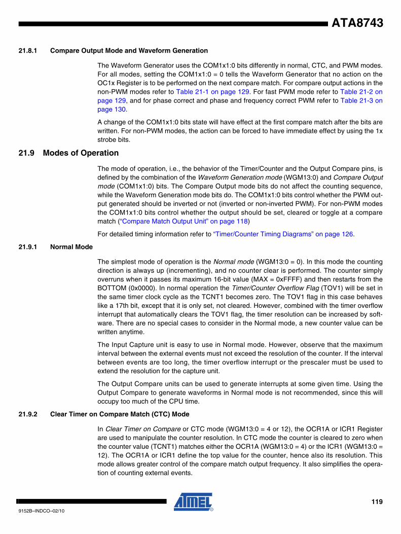
ATA8743
21.8.1 Compare Output Mode and Waveform Generation
The Waveform Generator uses the COM1x1:0 bits differently in normal, CTC, and PWM modes.For all modes, setting the COM1x1:0 = 0 tells the Waveform Generator that no action on theOC1x Register is to be performed on the next compare match. For compare output actions in thenon-PWM modes refer to Table 21-1 on page 129. For fast PWM mode refer to Table 21-2 onpage 129, and for phase correct and phase and frequency correct PWM refer to Table 21-3 onpage 130.
A change of the COM1x1:0 bits state will have effect at the first compare match after the bits arewritten. For non-PWM modes, the action can be forced to have immediate effect by using the 1xstrobe bits.
21.9 Modes of Operation
The mode of operation, i.e., the behavior of the Timer/Counter and the Output Compare pins, isdefined by the combination of the Waveform Generation mode (WGM13:0) and Compare Outputmode (COM1x1:0) bits. The Compare Output mode bits do not affect the counting sequence,while the Waveform Generation mode bits do. The COM1x1:0 bits control whether the PWM out-put generated should be inverted or not (inverted or non-inverted PWM). For non-PWM modesthe COM1x1:0 bits control whether the output should be set, cleared or toggle at a comparematch (“Compare Match Output Unit” on page 118)
For detailed timing information refer to “Timer/Counter Timing Diagrams” on page 126.
21.9.1 Normal Mode
The simplest mode of operation is the Normal mode (WGM13:0 = 0). In this mode the countingdirection is always up (incrementing), and no counter clear is performed. The counter simplyoverruns when it passes its maximum 16-bit value (MAX = 0xFFFF) and then restarts from theBOTTOM (0x0000). In normal operation the Timer/Counter Overflow Flag (TOV1) will be set inthe same timer clock cycle as the TCNT1 becomes zero. The TOV1 flag in this case behaveslike a 17th bit, except that it is only set, not cleared. However, combined with the timer overflowinterrupt that automatically clears the TOV1 flag, the timer resolution can be increased by soft-ware. There are no special cases to consider in the Normal mode, a new counter value can bewritten anytime.
The Input Capture unit is easy to use in Normal mode. However, observe that the maximuminterval between the external events must not exceed the resolution of the counter. If the intervalbetween events are too long, the timer overflow interrupt or the prescaler must be used toextend the resolution for the capture unit.
The Output Compare units can be used to generate interrupts at some given time. Using theOutput Compare to generate waveforms in Normal mode is not recommended, since this willoccupy too much of the CPU time.
21.9.2 Clear Timer on Compare Match (CTC) Mode
In Clear Timer on Compare or CTC mode (WGM13:0 = 4 or 12), the OCR1A or ICR1 Registerare used to manipulate the counter resolution. In CTC mode the counter is cleared to zero whenthe counter value (TCNT1) matches either the OCR1A (WGM13:0 = 4) or the ICR1 (WGM13:0 =12). The OCR1A or ICR1 define the top value for the counter, hence also its resolution. Thismode allows greater control of the compare match output frequency. It also simplifies the opera-tion of counting external events.
1199152B–INDCO–02/10
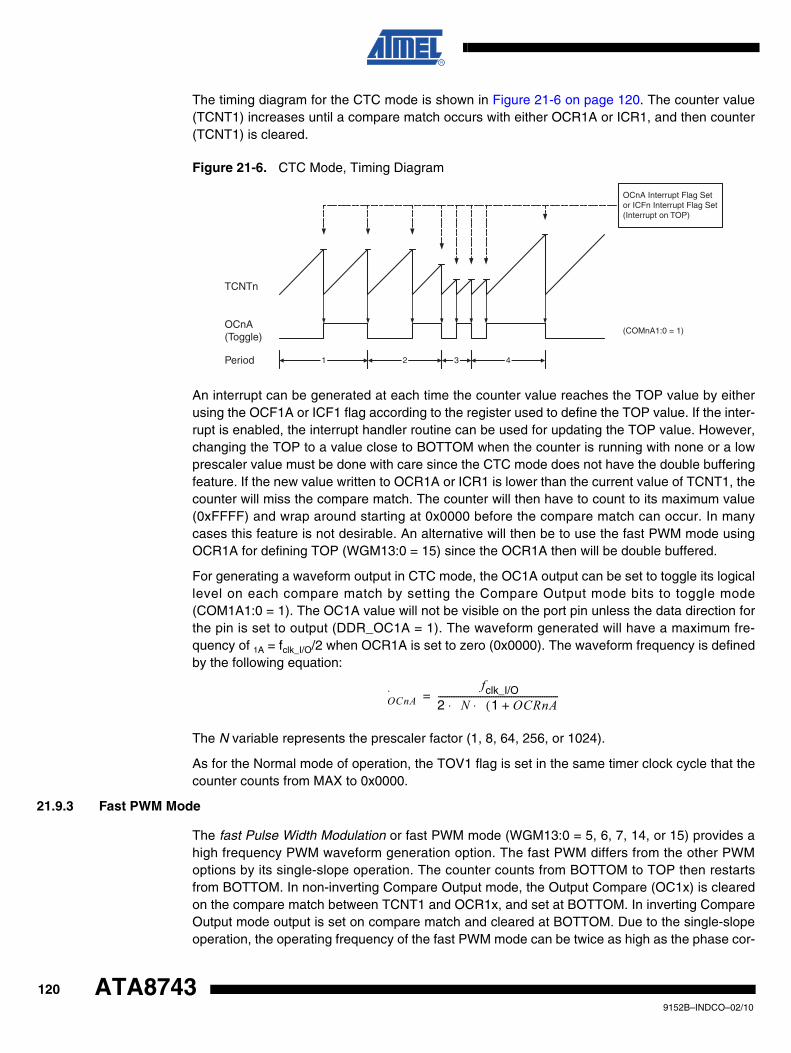
The timing diagram for the CTC mode is shown in Figure 21-6 on page 120. The counter value(TCNT1) increases until a compare match occurs with either OCR1A or ICR1, and then counter(TCNT1) is cleared.
Figure 21-6. CTC Mode, Timing Diagram
An interrupt can be generated at each time the counter value reaches the TOP value by eitherusing the OCF1A or ICF1 flag according to the register used to define the TOP value. If the inter-rupt is enabled, the interrupt handler routine can be used for updating the TOP value. However,changing the TOP to a value close to BOTTOM when the counter is running with none or a lowprescaler value must be done with care since the CTC mode does not have the double bufferingfeature. If the new value written to OCR1A or ICR1 is lower than the current value of TCNT1, thecounter will miss the compare match. The counter will then have to count to its maximum value(0xFFFF) and wrap around starting at 0x0000 before the compare match can occur. In manycases this feature is not desirable. An alternative will then be to use the fast PWM mode usingOCR1A for defining TOP (WGM13:0 = 15) since the OCR1A then will be double buffered.
For generating a waveform output in CTC mode, the OC1A output can be set to toggle its logicallevel on each compare match by setting the Compare Output mode bits to toggle mode(COM1A1:0 = 1). The OC1A value will not be visible on the port pin unless the data direction forthe pin is set to output (DDR_OC1A = 1). The waveform generated will have a maximum fre-quency of 1A = fclk_I/O/2 when OCR1A is set to zero (0x0000). The waveform frequency is definedby the following equation:
The N variable represents the prescaler factor (1, 8, 64, 256, or 1024).
As for the Normal mode of operation, the TOV1 flag is set in the same timer clock cycle that thecounter counts from MAX to 0x0000.
21.9.3 Fast PWM Mode
The fast Pulse Width Modulation or fast PWM mode (WGM13:0 = 5, 6, 7, 14, or 15) provides ahigh frequency PWM waveform generation option. The fast PWM differs from the other PWMoptions by its single-slope operation. The counter counts from BOTTOM to TOP then restartsfrom BOTTOM. In non-inverting Compare Output mode, the Output Compare (OC1x) is clearedon the compare match between TCNT1 and OCR1x, and set at BOTTOM. In inverting CompareOutput mode output is set on compare match and cleared at BOTTOM. Due to the single-slopeoperation, the operating frequency of the fast PWM mode can be twice as high as the phase cor-
TCNTn
OCnA(Toggle)
OCnA Interrupt Flag Setor ICFn Interrupt Flag Set(Interrupt on TOP)
1 4Period 2 3
(COMnA1:0 = 1)
fOCnAfclk_I/O
2 N 1 OCRnA+( )⋅ ⋅-------------------------------------------------------=
1209152B–INDCO–02/10
ATA8743
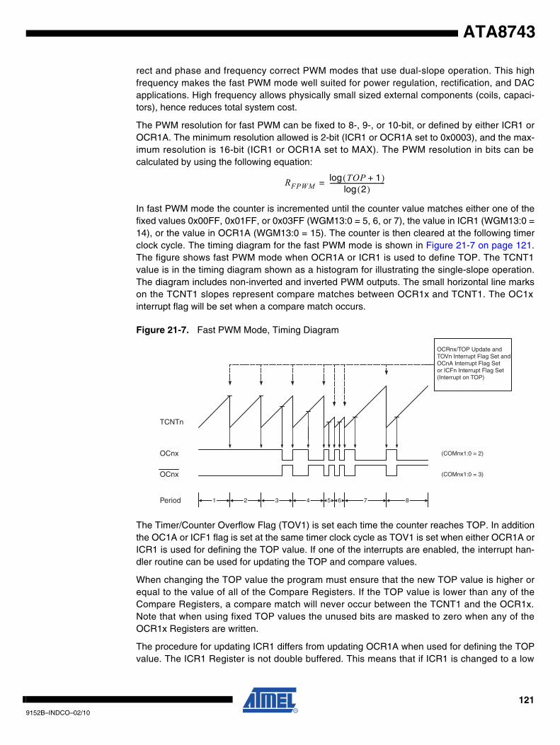
ATA8743
rect and phase and frequency correct PWM modes that use dual-slope operation. This highfrequency makes the fast PWM mode well suited for power regulation, rectification, and DACapplications. High frequency allows physically small sized external components (coils, capaci-tors), hence reduces total system cost.
The PWM resolution for fast PWM can be fixed to 8-, 9-, or 10-bit, or defined by either ICR1 orOCR1A. The minimum resolution allowed is 2-bit (ICR1 or OCR1A set to 0x0003), and the max-imum resolution is 16-bit (ICR1 or OCR1A set to MAX). The PWM resolution in bits can becalculated by using the following equation:
In fast PWM mode the counter is incremented until the counter value matches either one of thefixed values 0x00FF, 0x01FF, or 0x03FF (WGM13:0 = 5, 6, or 7), the value in ICR1 (WGM13:0 =14), or the value in OCR1A (WGM13:0 = 15). The counter is then cleared at the following timerclock cycle. The timing diagram for the fast PWM mode is shown in Figure 21-7 on page 121.The figure shows fast PWM mode when OCR1A or ICR1 is used to define TOP. The TCNT1value is in the timing diagram shown as a histogram for illustrating the single-slope operation.The diagram includes non-inverted and inverted PWM outputs. The small horizontal line markson the TCNT1 slopes represent compare matches between OCR1x and TCNT1. The OC1xinterrupt flag will be set when a compare match occurs.
Figure 21-7. Fast PWM Mode, Timing Diagram
The Timer/Counter Overflow Flag (TOV1) is set each time the counter reaches TOP. In additionthe OC1A or ICF1 flag is set at the same timer clock cycle as TOV1 is set when either OCR1A orICR1 is used for defining the TOP value. If one of the interrupts are enabled, the interrupt han-dler routine can be used for updating the TOP and compare values.
When changing the TOP value the program must ensure that the new TOP value is higher orequal to the value of all of the Compare Registers. If the TOP value is lower than any of theCompare Registers, a compare match will never occur between the TCNT1 and the OCR1x.Note that when using fixed TOP values the unused bits are masked to zero when any of theOCR1x Registers are written.
The procedure for updating ICR1 differs from updating OCR1A when used for defining the TOPvalue. The ICR1 Register is not double buffered. This means that if ICR1 is changed to a low
RFPWMTOP 1+( )log
2( )log-----------------------------------=
TCNTn
OCRnx/TOP Update andTOVn Interrupt Flag Set andOCnA Interrupt Flag Setor ICFn Interrupt Flag Set(Interrupt on TOP)
1 7Period 2 3 4 5 6 8
OCnx
OCnx
(COMnx1:0 = 2)
(COMnx1:0 = 3)
1219152B–INDCO–02/10
value when the counter is running with none or a low prescaler value, there is a risk that the newICR1 value written is lower than the current value of TCNT1. The result will then be that thecounter will miss the compare match at the TOP value. The counter will then have to count to theMAX value (0xFFFF) and wrap around starting at 0x0000 before the compare match can occur.The OCR1A Register however, is double buffered. This feature allows the OCR1A I/O locationto be written anytime. When the OCR1A I/O location is written the value written will be put intothe OCR1A Buffer Register. The OCR1A Compare Register will then be updated with the valuein the Buffer Register at the next timer clock cycle the TCNT1 matches TOP. The update is doneat the same timer clock cycle as the TCNT1 is cleared and the TOV1 flag is set.
Using the ICR1 Register for defining TOP works well when using fixed TOP values. By usingICR1, the OCR1A Register is free to be used for generating a PWM output on OC1A. However,if the base PWM frequency is actively changed (by changing the TOP value), using the OCR1Aas TOP is clearly a better choice due to its double buffer feature.
In fast PWM mode, the compare units allow generation of PWM waveforms on the OC1x pins.Setting the COM1x1:0 bits to two will produce a non-inverted PWM and an inverted PWM outputcan be generated by setting the COM1x1:0 to three (see Table 21-2 on page 129). The actualOC1x value will only be visible on the port pin if the data direction for the port pin is set as output(DDR_OC1x). The PWM waveform is generated by setting (or clearing) the OC1x Register atthe compare match between OCR1x and TCNT1, and clearing (or setting) the OC1x Register atthe timer clock cycle the counter is cleared (changes from TOP to BOTTOM).
The PWM frequency for the output can be calculated by the following equation:
The N variable represents the prescaler divider (1, 8, 64, 256, or 1024).
The extreme values for the OCR1x Register represents special cases when generating a PWMwaveform output in the fast PWM mode. If the OCR1x is set equal to BOTTOM (0x0000) the out-put will be a narrow spike for each TOP+1 timer clock cycle. Setting the OCR1x equal to TOPwill result in a constant high or low output (depending on the polarity of the output set by theCOM1x1:0 bits.)
A frequency (with 50% duty cycle) waveform output in fast PWM mode can be achieved by set-ting OC1A to toggle its logical level on each compare match (COM1A1:0 = 1). The waveformgenerated will have a maximum frequency of 1A = fclk_I/O/2 when OCR1A is set to zero (0x0000).This feature is similar to the OC1A toggle in CTC mode, except the double buffer feature of theOutput Compare unit is enabled in the fast PWM mode.
21.9.4 Phase Correct PWM Mode
The phase correct Pulse Width Modulation or phase correct PWM mode (WGM13:0 = 1, 2, 3,10, or 11) provides a high resolution phase correct PWM waveform generation option. Thephase correct PWM mode is, like the phase and frequency correct PWM mode, based on adual-slope operation. The counter counts repeatedly from BOTTOM (0x0000) to TOP and thenfrom TOP to BOTTOM. In non-inverting Compare Output mode, the Output Compare (OC1x) iscleared on the compare match between TCNT1 and OCR1x while upcounting, and set on thecompare match while downcounting. In inverting Output Compare mode, the operation isinverted. The dual-slope operation has lower maximum operation frequency than single slopeoperation. However, due to the symmetric feature of the dual-slope PWM modes, these modesare preferred for motor control applications.
fOCnxPWMfclk_I/O
N 1 TOP+( )⋅-------------------------------------=
1229152B–INDCO–02/10
ATA8743
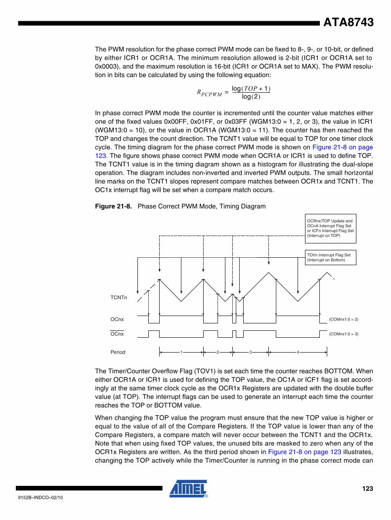
ATA8743
The PWM resolution for the phase correct PWM mode can be fixed to 8-, 9-, or 10-bit, or definedby either ICR1 or OCR1A. The minimum resolution allowed is 2-bit (ICR1 or OCR1A set to0x0003), and the maximum resolution is 16-bit (ICR1 or OCR1A set to MAX). The PWM resolu-tion in bits can be calculated by using the following equation:
In phase correct PWM mode the counter is incremented until the counter value matches eitherone of the fixed values 0x00FF, 0x01FF, or 0x03FF (WGM13:0 = 1, 2, or 3), the value in ICR1(WGM13:0 = 10), or the value in OCR1A (WGM13:0 = 11). The counter has then reached theTOP and changes the count direction. The TCNT1 value will be equal to TOP for one timer clockcycle. The timing diagram for the phase correct PWM mode is shown on Figure 21-8 on page123. The figure shows phase correct PWM mode when OCR1A or ICR1 is used to define TOP.The TCNT1 value is in the timing diagram shown as a histogram for illustrating the dual-slopeoperation. The diagram includes non-inverted and inverted PWM outputs. The small horizontalline marks on the TCNT1 slopes represent compare matches between OCR1x and TCNT1. TheOC1x interrupt flag will be set when a compare match occurs.
Figure 21-8. Phase Correct PWM Mode, Timing Diagram
The Timer/Counter Overflow Flag (TOV1) is set each time the counter reaches BOTTOM. Wheneither OCR1A or ICR1 is used for defining the TOP value, the OC1A or ICF1 flag is set accord-ingly at the same timer clock cycle as the OCR1x Registers are updated with the double buffervalue (at TOP). The interrupt flags can be used to generate an interrupt each time the counterreaches the TOP or BOTTOM value.
When changing the TOP value the program must ensure that the new TOP value is higher orequal to the value of all of the Compare Registers. If the TOP value is lower than any of theCompare Registers, a compare match will never occur between the TCNT1 and the OCR1x.Note that when using fixed TOP values, the unused bits are masked to zero when any of theOCR1x Registers are written. As the third period shown in Figure 21-8 on page 123 illustrates,changing the TOP actively while the Timer/Counter is running in the phase correct mode can
RPCPWMTOP 1+( )log
2( )log-----------------------------------=
OCRnx/TOP Update andOCnA Interrupt Flag Setor ICFn Interrupt Flag Set(Interrupt on TOP)
1 2 3 4
TOVn Interrupt Flag Set(Interrupt on Bottom)
TCNTn
Period
OCnx
OCnx
(COMnx1:0 = 2)
(COMnx1:0 = 3)
1239152B–INDCO–02/10
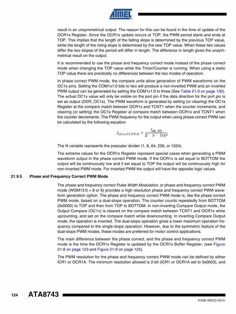
result in an unsymmetrical output. The reason for this can be found in the time of update of theOCR1x Register. Since the OCR1x update occurs at TOP, the PWM period starts and ends atTOP. This implies that the length of the falling slope is determined by the previous TOP value,while the length of the rising slope is determined by the new TOP value. When these two valuesdiffer the two slopes of the period will differ in length. The difference in length gives the unsym-metrical result on the output.
It is recommended to use the phase and frequency correct mode instead of the phase correctmode when changing the TOP value while the Timer/Counter is running. When using a staticTOP value there are practically no differences between the two modes of operation.
In phase correct PWM mode, the compare units allow generation of PWM waveforms on theOC1x pins. Setting the COM1x1:0 bits to two will produce a non-inverted PWM and an invertedPWM output can be generated by setting the COM1x1:0 to three (See Table 21-3 on page 130).The actual OC1x value will only be visible on the port pin if the data direction for the port pin isset as output (DDR_OC1x). The PWM waveform is generated by setting (or clearing) the OC1xRegister at the compare match between OCR1x and TCNT1 when the counter increments, andclearing (or setting) the OC1x Register at compare match between OCR1x and TCNT1 whenthe counter decrements. The PWM frequency for the output when using phase correct PWM canbe calculated by the following equation:
The N variable represents the prescaler divider (1, 8, 64, 256, or 1024).
The extreme values for the OCR1x Register represent special cases when generating a PWMwaveform output in the phase correct PWM mode. If the OCR1x is set equal to BOTTOM theoutput will be continuously low and if set equal to TOP the output will be continuously high fornon-inverted PWM mode. For inverted PWM the output will have the opposite logic values.
21.9.5 Phase and Frequency Correct PWM Mode
The phase and frequency correct Pulse Width Modulation, or phase and frequency correct PWMmode (WGM13:0 = 8 or 9) provides a high resolution phase and frequency correct PWM wave-form generation option. The phase and frequency correct PWM mode is, like the phase correctPWM mode, based on a dual-slope operation. The counter counts repeatedly from BOTTOM(0x0000) to TOP and then from TOP to BOTTOM. In non-inverting Compare Output mode, theOutput Compare (OC1x) is cleared on the compare match between TCNT1 and OCR1x whileupcounting, and set on the compare match while downcounting. In inverting Compare Outputmode, the operation is inverted. The dual-slope operation gives a lower maximum operation fre-quency compared to the single-slope operation. However, due to the symmetric feature of thedual-slope PWM modes, these modes are preferred for motor control applications.
The main difference between the phase correct, and the phase and frequency correct PWMmode is the time the OCR1x Register is updated by the OCR1x Buffer Register, (see Figure21-8 on page 123 and Figure 21-9 on page 125).
The PWM resolution for the phase and frequency correct PWM mode can be defined by eitherICR1 or OCR1A. The minimum resolution allowed is 2-bit (ICR1 or OCR1A set to 0x0003), and
fOCnxPCPWMfclk_I/O
2 N TOP⋅ ⋅---------------------------------=
1249152B–INDCO–02/10
ATA8743
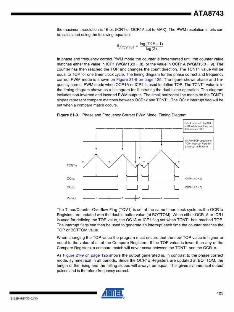
ATA8743
the maximum resolution is 16-bit (ICR1 or OCR1A set to MAX). The PWM resolution in bits canbe calculated using the following equation:
In phase and frequency correct PWM mode the counter is incremented until the counter valuematches either the value in ICR1 (WGM13:0 = 8), or the value in OCR1A (WGM13:0 = 9). Thecounter has then reached the TOP and changes the count direction. The TCNT1 value will beequal to TOP for one timer clock cycle. The timing diagram for the phase correct and frequencycorrect PWM mode is shown on Figure 21-9 on page 125. The figure shows phase and fre-quency correct PWM mode when OCR1A or ICR1 is used to define TOP. The TCNT1 value is inthe timing diagram shown as a histogram for illustrating the dual-slope operation. The diagramincludes non-inverted and inverted PWM outputs. The small horizontal line marks on the TCNT1slopes represent compare matches between OCR1x and TCNT1. The OC1x interrupt flag will beset when a compare match occurs.
Figure 21-9. Phase and Frequency Correct PWM Mode, Timing Diagram
The Timer/Counter Overflow Flag (TOV1) is set at the same timer clock cycle as the OCR1xRegisters are updated with the double buffer value (at BOTTOM). When either OCR1A or ICR1is used for defining the TOP value, the OC1A or ICF1 flag set when TCNT1 has reached TOP.The interrupt flags can then be used to generate an interrupt each time the counter reaches theTOP or BOTTOM value.
When changing the TOP value the program must ensure that the new TOP value is higher orequal to the value of all of the Compare Registers. If the TOP value is lower than any of theCompare Registers, a compare match will never occur between the TCNT1 and the OCR1x.
As Figure 21-9 on page 125 shows the output generated is, in contrast to the phase correctmode, symmetrical in all periods. Since the OCR1x Registers are updated at BOTTOM, thelength of the rising and the falling slopes will always be equal. This gives symmetrical outputpulses and is therefore frequency correct.
RPFCPWMTOP 1+( )log
2( )log-----------------------------------=
OCRnx/TOP UpdateandTOVn Interrupt Flag Set(Interrupt on Bottom)
OCnA Interrupt Flag Setor ICFn Interrupt Flag Set(Interrupt on TOP)
1 2 3 4
TCNTn
Period
OCnx
OCnx
(COMnx1:0 = 2)
(COMnx1:0 = 3)
1259152B–INDCO–02/10
Using the ICR1 Register for defining TOP works well when using fixed TOP values. By usingICR1, the OCR1A Register is free to be used for generating a PWM output on OC1A. However,if the base PWM frequency is actively changed by changing the TOP value, using the OCR1A asTOP is clearly a better choice due to its double buffer feature.
In phase and frequency correct PWM mode, the compare units allow generation of PWM wave-forms on the OC1x pins. Setting the COM1x1:0 bits to two will produce a non-inverted PWM andan inverted PWM output can be generated by setting the COM1x1:0 to three (See Table 21-3 onpage 130). The actual OC1x value will only be visible on the port pin if the data direction for theport pin is set as output (DDR_OC1x). The PWM waveform is generated by setting (or clearing)the OC1x Register at the compare match between OCR1x and TCNT1 when the counter incre-ments, and clearing (or setting) the OC1x Register at compare match between OCR1x andTCNT1 when the counter decrements. The PWM frequency for the output when using phaseand frequency correct PWM can be calculated by the following equation:
The N variable represents the prescaler divider (1, 8, 64, 256, or 1024).
The extreme values for the OCR1x Register represents special cases when generating a PWMwaveform output in the phase correct PWM mode. If the OCR1x is set equal to BOTTOM theoutput will be continuously low and if set equal to TOP the output will be set to high fornon-inverted PWM mode. For inverted PWM the output will have the opposite logic values.
21.10 Timer/Counter Timing Diagrams
The Timer/Counter is a synchronous design and the timer clock (clkT1) is therefore shown as aclock enable signal in the following figures. The figures include information on when interruptflags are set, and when the OCR1x Register is updated with the OCR1x buffer value (only formodes utilizing double buffering). Figure 21-10 on page 126 shows a timing diagram for the set-ting of OCF1x.
Figure 21-10. Timer/Counter Timing Diagram, Setting of OCF1x, no Prescaling
Figure 21-11 on page 127 shows the same timing data, but with the prescaler enabled.
fOCnxPFCPWMfclk_I/O
2 N TOP⋅ ⋅---------------------------------=
clkTn(clkI/O/1)
OCFnx
clkI/O
OCRnx
TCNTn
OCRnx Value
OCRnx - 1 OCRnx OCRnx + 1 OCRnx + 2
1269152B–INDCO–02/10
ATA8743
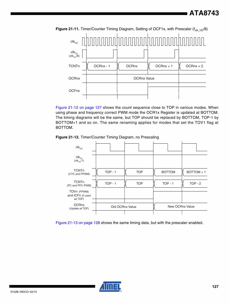
ATA8743
Figure 21-11. Timer/Counter Timing Diagram, Setting of OCF1x, with Prescaler (fclk_I/O/8)
Figure 21-12 on page 127 shows the count sequence close to TOP in various modes. Whenusing phase and frequency correct PWM mode the OCR1x Register is updated at BOTTOM.The timing diagrams will be the same, but TOP should be replaced by BOTTOM, TOP-1 byBOTTOM+1 and so on. The same renaming applies for modes that set the TOV1 flag atBOTTOM.
Figure 21-12. Timer/Counter Timing Diagram, no Prescaling
Figure 21-13 on page 128 shows the same timing data, but with the prescaler enabled.
OCFnx
OCRnx
TCNTn
OCRnx Value
OCRnx - 1 OCRnx OCRnx + 1 OCRnx + 2
clkI/O
clkTn(clkI/O/8)
TOVn (FPWM)and ICFn (if used
as TOP)
OCRnx(Update at TOP)
TCNTn(CTC and FPWM)
TCNTn(PC and PFC PWM)
TOP - 1 TOP TOP - 1 TOP - 2
Old OCRnx Value New OCRnx Value
TOP - 1 TOP BOTTOM BOTTOM + 1
clkTn(clkI/O/1)
clkI/O
1279152B–INDCO–02/10
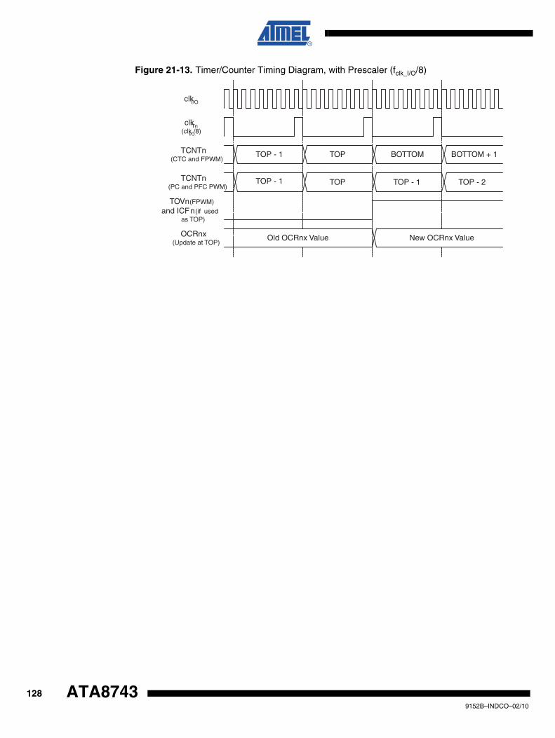
Figure 21-13. Timer/Counter Timing Diagram, with Prescaler (fclk_I/O/8)
TOVn (FPWM)and ICFn (if used
as TOP)
OCRnx(Update at TOP)
TCNTn(CTC and FPWM)
TCNTn(PC and PFC PWM)
TOP - 1 TOP TOP - 1 TOP - 2
Old OCRnx Value New OCRnx Value
TOP - 1 TOP BOTTOM BOTTOM + 1
clkI/O
clkTn(clkI/O/8)
1289152B–INDCO–02/10
ATA8743
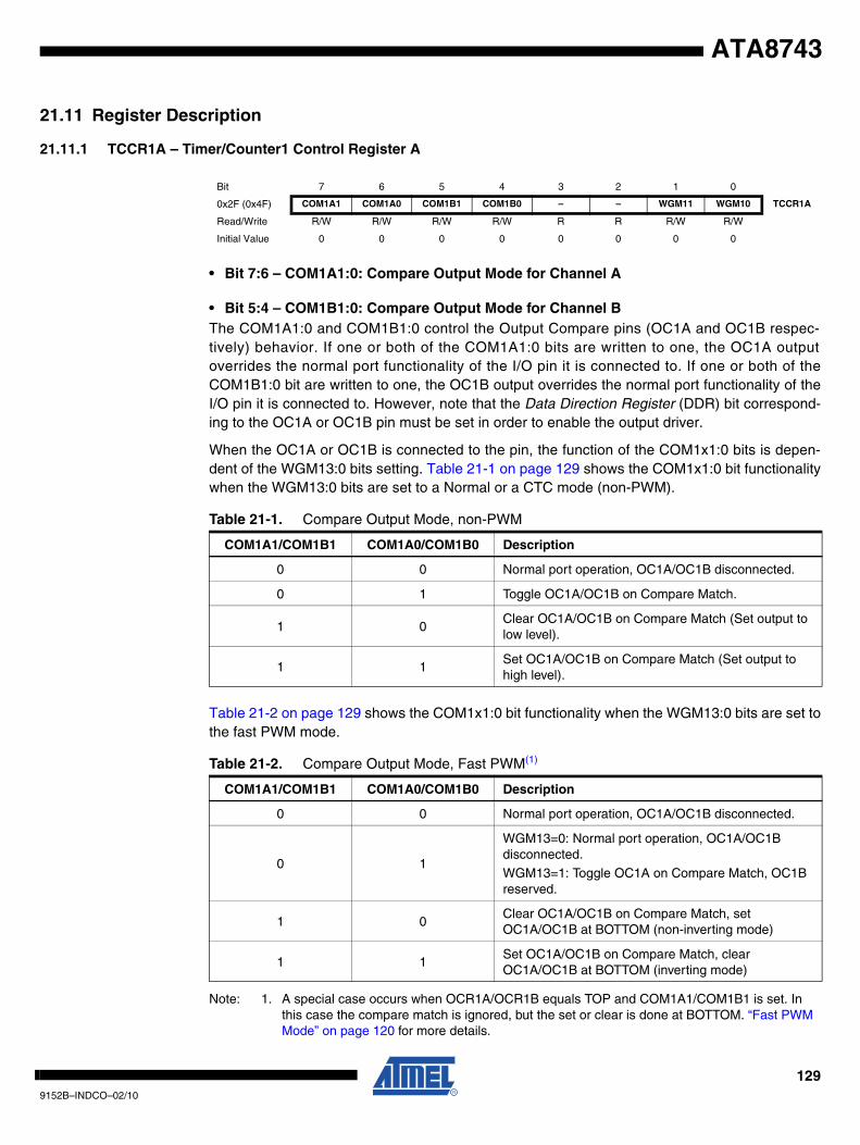
ATA8743
21.11 Register Description
21.11.1 TCCR1A – Timer/Counter1 Control Register A
• Bit 7:6 – COM1A1:0: Compare Output Mode for Channel A
• Bit 5:4 – COM1B1:0: Compare Output Mode for Channel BThe COM1A1:0 and COM1B1:0 control the Output Compare pins (OC1A and OC1B respec-tively) behavior. If one or both of the COM1A1:0 bits are written to one, the OC1A outputoverrides the normal port functionality of the I/O pin it is connected to. If one or both of theCOM1B1:0 bit are written to one, the OC1B output overrides the normal port functionality of theI/O pin it is connected to. However, note that the Data Direction Register (DDR) bit correspond-ing to the OC1A or OC1B pin must be set in order to enable the output driver.
When the OC1A or OC1B is connected to the pin, the function of the COM1x1:0 bits is depen-dent of the WGM13:0 bits setting. Table 21-1 on page 129 shows the COM1x1:0 bit functionalitywhen the WGM13:0 bits are set to a Normal or a CTC mode (non-PWM).
Table 21-2 on page 129 shows the COM1x1:0 bit functionality when the WGM13:0 bits are set tothe fast PWM mode.
Note: 1. A special case occurs when OCR1A/OCR1B equals TOP and COM1A1/COM1B1 is set. In this case the compare match is ignored, but the set or clear is done at BOTTOM. “Fast PWM Mode” on page 120 for more details.
Bit 7 6 5 4 3 2 1 0
0x2F (0x4F) COM1A1 COM1A0 COM1B1 COM1B0 – – WGM11 WGM10 TCCR1A
Read/Write R/W R/W R/W R/W R R R/W R/W
Initial Value 0 0 0 0 0 0 0 0
Table 21-1. Compare Output Mode, non-PWM
COM1A1/COM1B1 COM1A0/COM1B0 Description
0 0 Normal port operation, OC1A/OC1B disconnected.
0 1 Toggle OC1A/OC1B on Compare Match.
1 0Clear OC1A/OC1B on Compare Match (Set output to low level).
1 1Set OC1A/OC1B on Compare Match (Set output to high level).
Table 21-2. Compare Output Mode, Fast PWM(1)
COM1A1/COM1B1 COM1A0/COM1B0 Description
0 0 Normal port operation, OC1A/OC1B disconnected.
0 1
WGM13=0: Normal port operation, OC1A/OC1B disconnected.WGM13=1: Toggle OC1A on Compare Match, OC1B reserved.
1 0Clear OC1A/OC1B on Compare Match, set OC1A/OC1B at BOTTOM (non-inverting mode)
1 1Set OC1A/OC1B on Compare Match, clear OC1A/OC1B at BOTTOM (inverting mode)
1299152B–INDCO–02/10
Table 21-3 shows the COM1x1:0 bit functionality when the WGM13:0 bits are set to the phasecorrect or the phase and frequency correct, PWM mode.
Note: A special case occurs when OCR1A/OCR1B equals TOP and COM1A1/COM1B1 is set. “Phase Correct PWM Mode” on page 122 for more details.
• Bit 1:0 – WGM11:0: Waveform Generation ModeCombined with the WGM13:2 bits found in the TCCR1B Register, these bits control the countingsequence of the counter, the source for maximum (TOP) counter value, and what type of wave-form generation to be used, see Table 21-4 on page 131. Modes of operation supported by theTimer/Counter unit are: Normal mode (counter), Clear Timer on Compare match (CTC) mode,and three types of Pulse Width Modulation (PWM) modes. (“Modes of Operation” on page 119).
Table 21-3. Compare Output Mode, Phase Correct and Phase and Frequency Correct PWM(Note:)
COM1A1/COM1B1 COM1A0/COM1B0 Description
0 0 Normal port operation, OC1A/OC1B disconnected.
0 1
WGM13=0: Normal port operation, OC1A/OC1B disconnected.WGM13=1: Toggle OC1A on Compare Match, OC1B reserved.
1 0Clear OC1A/OC1B on Compare Match when up-counting. Set OC1A/OC1B on Compare Match when downcounting.
1 1Set OC1A/OC1B on Compare Match when up-counting. Clear OC1A/OC1B on Compare Match when downcounting.
1309152B–INDCO–02/10
ATA8743
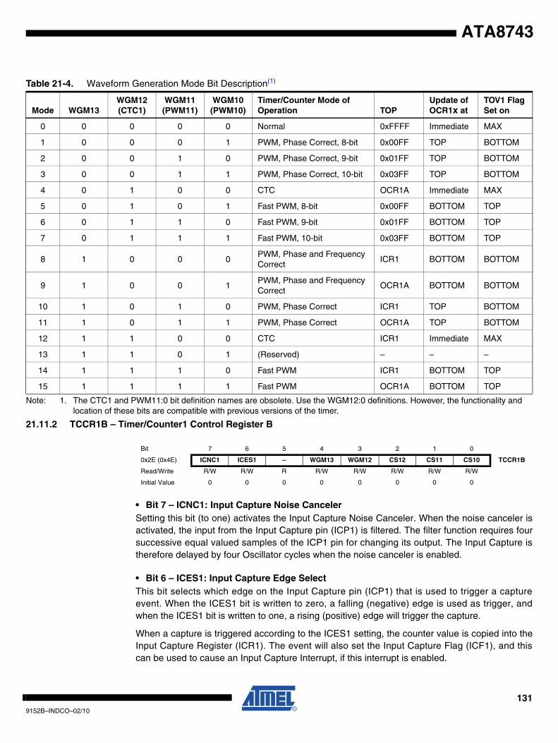
ATA8743
Note: 1. The CTC1 and PWM11:0 bit definition names are obsolete. Use the WGM12:0 definitions. However, the functionality and location of these bits are compatible with previous versions of the timer.
21.11.2 TCCR1B – Timer/Counter1 Control Register B
• Bit 7 – ICNC1: Input Capture Noise CancelerSetting this bit (to one) activates the Input Capture Noise Canceler. When the noise canceler isactivated, the input from the Input Capture pin (ICP1) is filtered. The filter function requires foursuccessive equal valued samples of the ICP1 pin for changing its output. The Input Capture istherefore delayed by four Oscillator cycles when the noise canceler is enabled.
• Bit 6 – ICES1: Input Capture Edge SelectThis bit selects which edge on the Input Capture pin (ICP1) that is used to trigger a captureevent. When the ICES1 bit is written to zero, a falling (negative) edge is used as trigger, andwhen the ICES1 bit is written to one, a rising (positive) edge will trigger the capture.
When a capture is triggered according to the ICES1 setting, the counter value is copied into theInput Capture Register (ICR1). The event will also set the Input Capture Flag (ICF1), and thiscan be used to cause an Input Capture Interrupt, if this interrupt is enabled.
Table 21-4. Waveform Generation Mode Bit Description(1)
Mode WGM13WGM12(CTC1)
WGM11(PWM11)
WGM10(PWM10)
Timer/Counter Mode of Operation TOP
Update of OCR1x at
TOV1 Flag Set on
0 0 0 0 0 Normal 0xFFFF Immediate MAX
1 0 0 0 1 PWM, Phase Correct, 8-bit 0x00FF TOP BOTTOM
2 0 0 1 0 PWM, Phase Correct, 9-bit 0x01FF TOP BOTTOM
3 0 0 1 1 PWM, Phase Correct, 10-bit 0x03FF TOP BOTTOM
4 0 1 0 0 CTC OCR1A Immediate MAX
5 0 1 0 1 Fast PWM, 8-bit 0x00FF BOTTOM TOP
6 0 1 1 0 Fast PWM, 9-bit 0x01FF BOTTOM TOP
7 0 1 1 1 Fast PWM, 10-bit 0x03FF BOTTOM TOP
8 1 0 0 0PWM, Phase and Frequency Correct
ICR1 BOTTOM BOTTOM
9 1 0 0 1PWM, Phase and Frequency Correct
OCR1A BOTTOM BOTTOM
10 1 0 1 0 PWM, Phase Correct ICR1 TOP BOTTOM
11 1 0 1 1 PWM, Phase Correct OCR1A TOP BOTTOM
12 1 1 0 0 CTC ICR1 Immediate MAX
13 1 1 0 1 (Reserved) – – –
14 1 1 1 0 Fast PWM ICR1 BOTTOM TOP
15 1 1 1 1 Fast PWM OCR1A BOTTOM TOP
Bit 7 6 5 4 3 2 1 0
0x2E (0x4E) ICNC1 ICES1 – WGM13 WGM12 CS12 CS11 CS10 TCCR1B
Read/Write R/W R/W R R/W R/W R/W R/W R/W
Initial Value 0 0 0 0 0 0 0 0
1319152B–INDCO–02/10
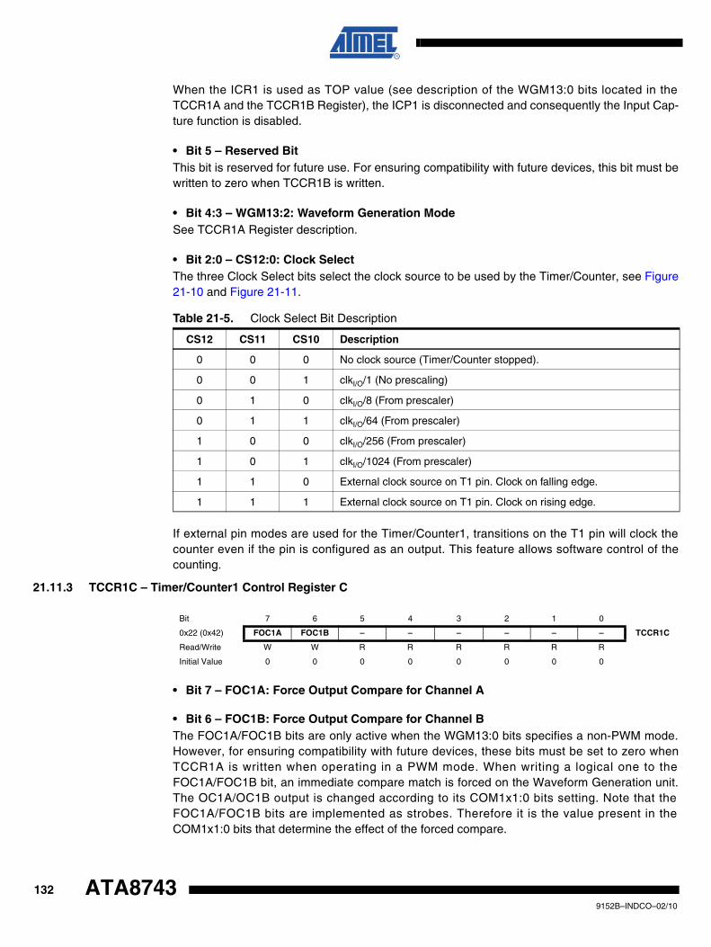
When the ICR1 is used as TOP value (see description of the WGM13:0 bits located in theTCCR1A and the TCCR1B Register), the ICP1 is disconnected and consequently the Input Cap-ture function is disabled.
• Bit 5 – Reserved BitThis bit is reserved for future use. For ensuring compatibility with future devices, this bit must bewritten to zero when TCCR1B is written.
• Bit 4:3 – WGM13:2: Waveform Generation ModeSee TCCR1A Register description.
• Bit 2:0 – CS12:0: Clock SelectThe three Clock Select bits select the clock source to be used by the Timer/Counter, see Figure21-10 and Figure 21-11.
If external pin modes are used for the Timer/Counter1, transitions on the T1 pin will clock thecounter even if the pin is configured as an output. This feature allows software control of thecounting.
21.11.3 TCCR1C – Timer/Counter1 Control Register C
• Bit 7 – FOC1A: Force Output Compare for Channel A
• Bit 6 – FOC1B: Force Output Compare for Channel BThe FOC1A/FOC1B bits are only active when the WGM13:0 bits specifies a non-PWM mode.However, for ensuring compatibility with future devices, these bits must be set to zero whenTCCR1A is written when operating in a PWM mode. When writing a logical one to theFOC1A/FOC1B bit, an immediate compare match is forced on the Waveform Generation unit.The OC1A/OC1B output is changed according to its COM1x1:0 bits setting. Note that theFOC1A/FOC1B bits are implemented as strobes. Therefore it is the value present in theCOM1x1:0 bits that determine the effect of the forced compare.
Table 21-5. Clock Select Bit Description
CS12 CS11 CS10 Description
0 0 0 No clock source (Timer/Counter stopped).
0 0 1 clkI/O/1 (No prescaling)
0 1 0 clkI/O/8 (From prescaler)
0 1 1 clkI/O/64 (From prescaler)
1 0 0 clkI/O/256 (From prescaler)
1 0 1 clkI/O/1024 (From prescaler)
1 1 0 External clock source on T1 pin. Clock on falling edge.
1 1 1 External clock source on T1 pin. Clock on rising edge.
Bit 7 6 5 4 3 2 1 0
0x22 (0x42) FOC1A FOC1B – – – – – – TCCR1C
Read/Write W W R R R R R R
Initial Value 0 0 0 0 0 0 0 0
1329152B–INDCO–02/10
ATA8743
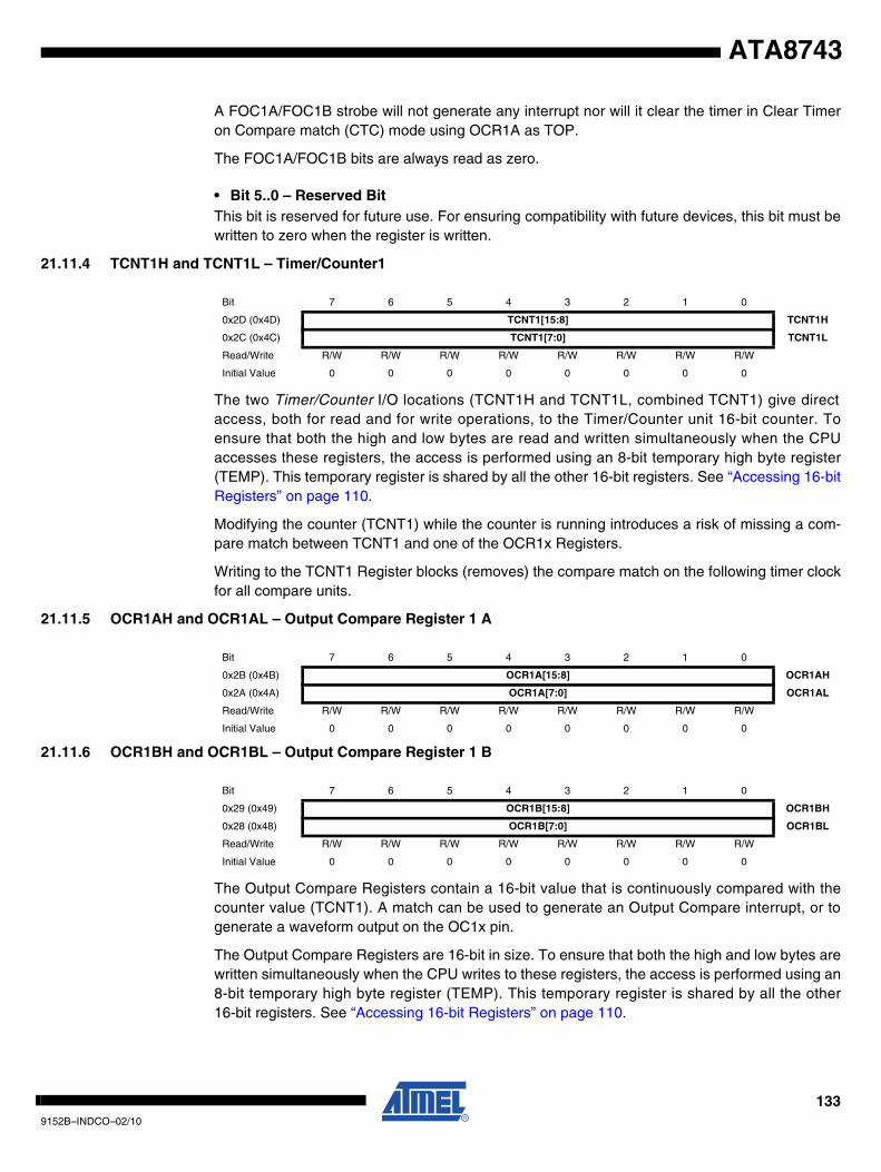
ATA8743
A FOC1A/FOC1B strobe will not generate any interrupt nor will it clear the timer in Clear Timeron Compare match (CTC) mode using OCR1A as TOP.
The FOC1A/FOC1B bits are always read as zero.
• Bit 5..0 – Reserved BitThis bit is reserved for future use. For ensuring compatibility with future devices, this bit must bewritten to zero when the register is written.
21.11.4 TCNT1H and TCNT1L – Timer/Counter1
The two Timer/Counter I/O locations (TCNT1H and TCNT1L, combined TCNT1) give directaccess, both for read and for write operations, to the Timer/Counter unit 16-bit counter. Toensure that both the high and low bytes are read and written simultaneously when the CPUaccesses these registers, the access is performed using an 8-bit temporary high byte register(TEMP). This temporary register is shared by all the other 16-bit registers. See “Accessing 16-bitRegisters” on page 110.
Modifying the counter (TCNT1) while the counter is running introduces a risk of missing a com-pare match between TCNT1 and one of the OCR1x Registers.
Writing to the TCNT1 Register blocks (removes) the compare match on the following timer clockfor all compare units.
21.11.5 OCR1AH and OCR1AL – Output Compare Register 1 A
21.11.6 OCR1BH and OCR1BL – Output Compare Register 1 B
The Output Compare Registers contain a 16-bit value that is continuously compared with thecounter value (TCNT1). A match can be used to generate an Output Compare interrupt, or togenerate a waveform output on the OC1x pin.
The Output Compare Registers are 16-bit in size. To ensure that both the high and low bytes arewritten simultaneously when the CPU writes to these registers, the access is performed using an8-bit temporary high byte register (TEMP). This temporary register is shared by all the other16-bit registers. See “Accessing 16-bit Registers” on page 110.
Bit 7 6 5 4 3 2 1 0
0x2D (0x4D) TCNT1[15:8] TCNT1H
0x2C (0x4C) TCNT1[7:0] TCNT1L
Read/Write R/W R/W R/W R/W R/W R/W R/W R/W
Initial Value 0 0 0 0 0 0 0 0
Bit 7 6 5 4 3 2 1 0
0x2B (0x4B) OCR1A[15:8] OCR1AH
0x2A (0x4A) OCR1A[7:0] OCR1AL
Read/Write R/W R/W R/W R/W R/W R/W R/W R/W
Initial Value 0 0 0 0 0 0 0 0
Bit 7 6 5 4 3 2 1 0
0x29 (0x49) OCR1B[15:8] OCR1BH
0x28 (0x48) OCR1B[7:0] OCR1BL
Read/Write R/W R/W R/W R/W R/W R/W R/W R/W
Initial Value 0 0 0 0 0 0 0 0
1339152B–INDCO–02/10
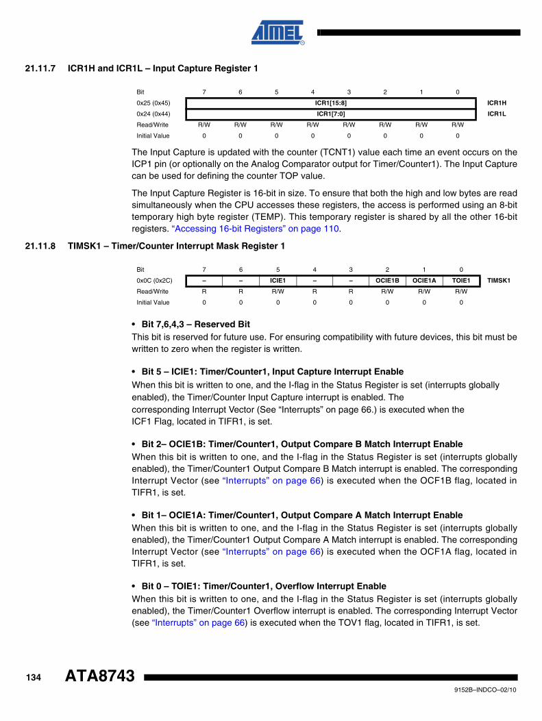
21.11.7 ICR1H and ICR1L – Input Capture Register 1
The Input Capture is updated with the counter (TCNT1) value each time an event occurs on theICP1 pin (or optionally on the Analog Comparator output for Timer/Counter1). The Input Capturecan be used for defining the counter TOP value.
The Input Capture Register is 16-bit in size. To ensure that both the high and low bytes are readsimultaneously when the CPU accesses these registers, the access is performed using an 8-bittemporary high byte register (TEMP). This temporary register is shared by all the other 16-bitregisters. “Accessing 16-bit Registers” on page 110.
21.11.8 TIMSK1 – Timer/Counter Interrupt Mask Register 1
• Bit 7,6,4,3 – Reserved BitThis bit is reserved for future use. For ensuring compatibility with future devices, this bit must bewritten to zero when the register is written.
• Bit 5 – ICIE1: Timer/Counter1, Input Capture Interrupt EnableWhen this bit is written to one, and the I-flag in the Status Register is set (interrupts globally enabled), the Timer/Counter Input Capture interrupt is enabled. Thecorresponding Interrupt Vector (See “Interrupts” on page 66.) is executed when theICF1 Flag, located in TIFR1, is set.
• Bit 2– OCIE1B: Timer/Counter1, Output Compare B Match Interrupt EnableWhen this bit is written to one, and the I-flag in the Status Register is set (interrupts globallyenabled), the Timer/Counter1 Output Compare B Match interrupt is enabled. The correspondingInterrupt Vector (see “Interrupts” on page 66) is executed when the OCF1B flag, located inTIFR1, is set.
• Bit 1– OCIE1A: Timer/Counter1, Output Compare A Match Interrupt EnableWhen this bit is written to one, and the I-flag in the Status Register is set (interrupts globallyenabled), the Timer/Counter1 Output Compare A Match interrupt is enabled. The correspondingInterrupt Vector (see “Interrupts” on page 66) is executed when the OCF1A flag, located inTIFR1, is set.
• Bit 0 – TOIE1: Timer/Counter1, Overflow Interrupt Enable When this bit is written to one, and the I-flag in the Status Register is set (interrupts globallyenabled), the Timer/Counter1 Overflow interrupt is enabled. The corresponding Interrupt Vector(see “Interrupts” on page 66) is executed when the TOV1 flag, located in TIFR1, is set.
Bit 7 6 5 4 3 2 1 0
0x25 (0x45) ICR1[15:8] ICR1H
0x24 (0x44) ICR1[7:0] ICR1L
Read/Write R/W R/W R/W R/W R/W R/W R/W R/W
Initial Value 0 0 0 0 0 0 0 0
Bit 7 6 5 4 3 2 1 0
0x0C (0x2C) – – ICIE1 – – OCIE1B OCIE1A TOIE1 TIMSK1
Read/Write R R R/W R R R/W R/W R/W
Initial Value 0 0 0 0 0 0 0 0
1349152B–INDCO–02/10
ATA8743
ATA8743
21.11.9 TIFR1 – Timer/Counter Interrupt Flag Register 1
• Bit 7,6,4,3 – Reserved BitThis bit is reserved for future use. For ensuring compatibility with future devices, this bit must bewritten to zero when the register is written.
• Bit 5– ICF1: Timer/Counter1, Input Capture FlagThis flag is set when a capture event occurs on the ICP1 pin. When the Input Capture Register(ICR1) is set by the WGM13:0 to be used as the TOP value, the ICF1 flag is set when the coun-ter reaches the TOP value.
ICF1 is automatically cleared when the Input Capture Interrupt Vector is executed. Alternatively,ICF1 can be cleared by writing a logic one to its bit location.
• Bit 2– OCF1B: Timer/Counter1, Output Compare B Match FlagThis flag is set in the timer clock cycle after the counter (TCNT1) value matches the OutputCompare Register B (OCR1B).
Note that a Forced Output Compare (1B) strobe will not set the OCF1B flag.
OCF1B is automatically cleared when the Output Compare Match B Interrupt Vector is exe-cuted. Alternatively, OCF1B can be cleared by writing a logic one to its bit location.
• Bit 1– OCF1A: Timer/Counter1, Output Compare A Match FlagThis flag is set in the timer clock cycle after the counter (TCNT1) value matches the OutputCompare Register A (OCR1A).
Note that a Forced Output Compare (1A) strobe will not set the OCF1A flag.
OCF1A is automatically cleared when the Output Compare Match A Interrupt Vector is exe-cuted. Alternatively, OCF1A can be cleared by writing a logic one to its bit location.
• Bit 0– TOV1: Timer/Counter1, Overflow FlagThe setting of this flag is dependent of the WGM13:0 bits setting. In Normal and CTC modes,the TOV1 flag is set when the timer overflows. See Table 21-4 on page 131 for the TOV1 flagbehavior when using another WGM13:0 bit setting.
TOV1 is automatically cleared when the Timer/Counter1 Overflow Interrupt Vector is executed.Alternatively, TOV1 can be cleared by writing a logic one to its bit location.
Bit 7 6 5 4 3 2 1 0
0x0B (0x2B) – – ICIF1 – – OCF1B OCF1A TOV1 TIFR1
Read/Write R R R/W R R R/W R/W R/W
Initial Value 0 0 0 0 0 0 0 0
1359152B–INDCO–02/10
22. Timer/Counter Prescaler
Timer/Counter 0, and 1 share the same prescaler module, but the Timer/Counters can have dif-ferent prescaler settings. The description below applies to all Timer/Counters. Tn is used as ageneral name, n = 0, 1.
The Timer/Counter can be clocked directly by the system clock (by setting the CSn2:0 = 1). Thisprovides the fastest operation, with a maximum Timer/Counter clock frequency equal to systemclock frequency (fCLK_I/O). Alternatively, one of four taps from the prescaler can be used as aclock source. The prescaled clock has a frequency of either fCLK_I/O/8, fCLK_I/O/64, fCLK_I/O/256, orfCLK_I/O/1024.
22.0.1 Prescaler Reset
The prescaler is free running, i.e., operates independently of the Clock Select logic of theTimer/CounterCounter, and it is shared by the Timer/Counter Tn. Since the prescaler is notaffected by the Timer/Counter’s clock select, the state of the prescaler will have implications forsituations where a prescaled clock is used. One example of prescaling artifacts occurs when thetimer is enabled and clocked by the prescaler (6 > CSn2:0 > 1). The number of system clockcycles from when the timer is enabled to the first count occurs can be from 1 to N+1 systemclock cycles, where N equals the prescaler divisor (8, 64, 256, or 1024).
It is possible to use the Prescaler Reset for synchronizing the Timer/Counter to programexecution.
22.0.2 External Clock Source
An external clock source applied to the Tn pin can be used as Timer/Counter clock (clkTn). TheTn pin is sampled once every system clock cycle by the pin synchronization logic. The synchro-nized (sampled) signal is then passed through the edge detector. Figure 22-1 on page 136shows a functional equivalent block diagram of the Tn synchronization and edge detector logic.The registers are clocked at the positive edge of the internal system clock (clkI/O). The latch istransparent in the high period of the internal system clock.
The edge detector generates one clkT0 pulse for each positive (CSn2:0 = 7) or negative (CSn2:0= 6) edge it detects.
Figure 22-1. T0 Pin Sampling
The synchronization and edge detector logic introduces a delay of 2.5 to 3.5 system clock cyclesfrom an edge has been applied to the Tn pin to the counter is updated.
Enabling and disabling of the clock input must be done when Tn has been stable for at least onesystem clock cycle, otherwise it is a risk that a false Timer/Counter clock pulse is generated.
Each half period of the external clock applied must be longer than one system clock cycle toensure correct sampling. The external clock must be guaranteed to have less than half the sys-
Tn_sync(To ClockSelect Logic)
Edge DetectorSynchronization
D QD Q
LE
D QTn
clkI/O
1369152B–INDCO–02/10
ATA8743
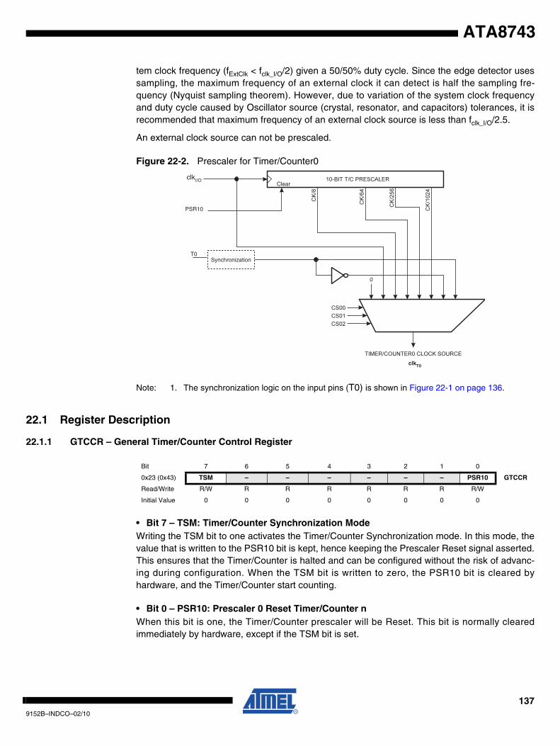
ATA8743
tem clock frequency (fExtClk < fclk_I/O/2) given a 50/50% duty cycle. Since the edge detector usessampling, the maximum frequency of an external clock it can detect is half the sampling fre-quency (Nyquist sampling theorem). However, due to variation of the system clock frequencyand duty cycle caused by Oscillator source (crystal, resonator, and capacitors) tolerances, it isrecommended that maximum frequency of an external clock source is less than fclk_I/O/2.5.
An external clock source can not be prescaled.
Figure 22-2. Prescaler for Timer/Counter0
Note: 1. The synchronization logic on the input pins (T0) is shown in Figure 22-1 on page 136.
22.1 Register Description
22.1.1 GTCCR – General Timer/Counter Control Register
• Bit 7 – TSM: Timer/Counter Synchronization ModeWriting the TSM bit to one activates the Timer/Counter Synchronization mode. In this mode, thevalue that is written to the PSR10 bit is kept, hence keeping the Prescaler Reset signal asserted.This ensures that the Timer/Counter is halted and can be configured without the risk of advanc-ing during configuration. When the TSM bit is written to zero, the PSR10 bit is cleared byhardware, and the Timer/Counter start counting.
• Bit 0 – PSR10: Prescaler 0 Reset Timer/Counter nWhen this bit is one, the Timer/Counter prescaler will be Reset. This bit is normally clearedimmediately by hardware, except if the TSM bit is set.
PSR10
Clear
clkT0
T0
clkI/O
Synchronization
Bit 7 6 5 4 3 2 1 0
0x23 (0x43) TSM – – – – – – PSR10 GTCCR
Read/Write R/W R R R R R R R/W
Initial Value 0 0 0 0 0 0 0 0
1379152B–INDCO–02/10
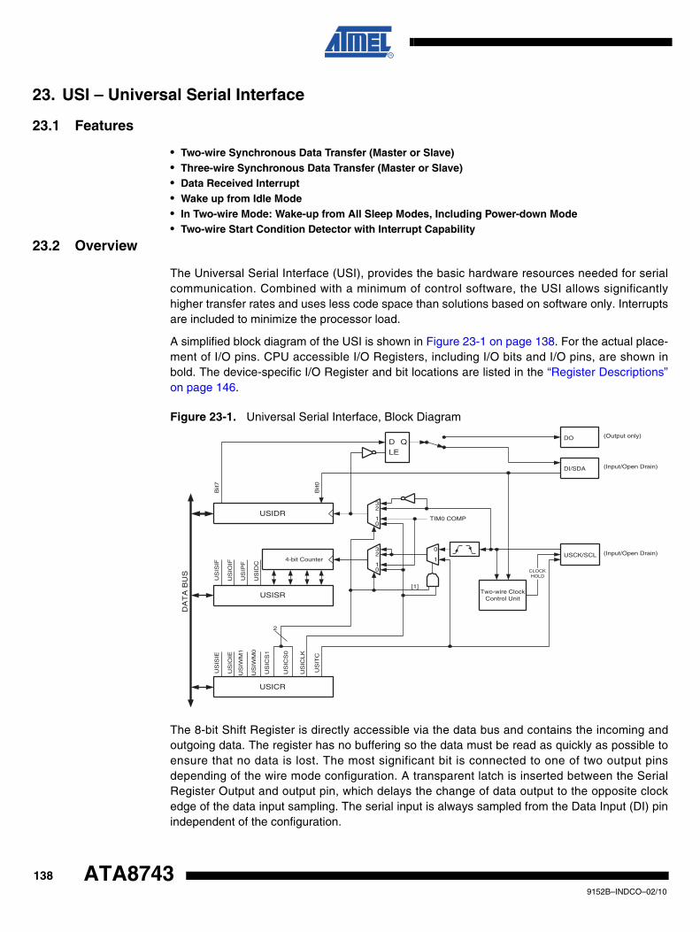
23. USI – Universal Serial Interface
23.1 Features
• Two-wire Synchronous Data Transfer (Master or Slave)• Three-wire Synchronous Data Transfer (Master or Slave)• Data Received Interrupt• Wake up from Idle Mode• In Two-wire Mode: Wake-up from All Sleep Modes, Including Power-down Mode• Two-wire Start Condition Detector with Interrupt Capability
23.2 Overview
The Universal Serial Interface (USI), provides the basic hardware resources needed for serialcommunication. Combined with a minimum of control software, the USI allows significantlyhigher transfer rates and uses less code space than solutions based on software only. Interruptsare included to minimize the processor load.
A simplified block diagram of the USI is shown in Figure 23-1 on page 138. For the actual place-ment of I/O pins. CPU accessible I/O Registers, including I/O bits and I/O pins, are shown inbold. The device-specific I/O Register and bit locations are listed in the “Register Descriptions”on page 146.
Figure 23-1. Universal Serial Interface, Block Diagram
The 8-bit Shift Register is directly accessible via the data bus and contains the incoming andoutgoing data. The register has no buffering so the data must be read as quickly as possible toensure that no data is lost. The most significant bit is connected to one of two output pinsdepending of the wire mode configuration. A transparent latch is inserted between the SerialRegister Output and output pin, which delays the change of data output to the opposite clockedge of the data input sampling. The serial input is always sampled from the Data Input (DI) pinindependent of the configuration.
DA
TA
BU
S
US
IPF
US
ITC
US
ICLK
US
ICS
0
US
ICS
1
US
IOIF
US
IOIE
US
IDC
US
ISIF
US
IWM
0
US
IWM
1
US
ISIE
Bit7
Two-wire ClockControl Unit
DO (Output only)
DI/SDA (Input/Open Drain)
USCK/SCL (Input/Open Drain)4-bit Counter
USIDR
USISR
D QLE
USICR
CLOCKHOLD
TIM0 COMP
Bit0
[1]
3
01
2
3
01
2
0
1
2
1389152B–INDCO–02/10
ATA8743
ATA8743
The 4-bit counter can be both read and written via the data bus, and can generate an overflowinterrupt. Both the Serial Register and the counter are clocked simultaneously by the same clocksource. This allows the counter to count the number of bits received or transmitted and generatean interrupt when the transfer is complete. Note that when an external clock source is selectedthe counter counts both clock edges. In this case the counter counts the number of edges, andnot the number of bits. The clock can be selected from three different sources: The USCK pin,Timer/Counter0 Compare Match or from software.
The Two-wire clock control unit can generate an interrupt when a start condition is detected onthe Two-wire bus. It can also generate wait states by holding the clock pin low after a start con-dition is detected, or after the counter overflows.
23.3 Functional Descriptions
23.3.1 Three-wire Mode
The USI Three-wire mode is compliant to the Serial Peripheral Interface (SPI) mode 0 and 1, butdoes not have the slave select (SS) pin functionality. However, this feature can be implementedin software if necessary. Pin names used by this mode are: DI, DO, and USCK.
Figure 23-2. Three-wire Mode Operation, Simplified Diagram
Figure 23-2 on page 139 shows two USI units operating in Three-wire mode, one as Master andone as Slave. The two Shift Registers are interconnected in such way that after eight USCKclocks, the data in each register are interchanged. The same clock also increments the USI’s4-bit counter. The Counter Overflow (interrupt) Flag, or USIOIF, can therefore be used to deter-mine when a transfer is completed. The clock is generated by the Master device software bytoggling the USCK pin via the PORT Register or by writing a one to the USITC bit in USICR.
SLAVE
MASTER
Bit7 Bit6 Bit5 Bit4 Bit3 Bit2 Bit1 Bit0
DO
DI
USCK
Bit7 Bit6 Bit5 Bit4 Bit3 Bit2 Bit1 Bit0
DO
DI
USCK
PORTxn
1399152B–INDCO–02/10
Figure 23-3. Three-wire Mode, Timing Diagram
The Three-wire mode timing is shown in Figure 23-3 on page 140. At the top of the figure is aUSCK cycle reference. One bit is shifted into the USI Shift Register (USIDR) for each of thesecycles. The USCK timing is shown for both external clock modes. In External Clock mode 0(USICS0 = 0), DI is sampled at positive edges, and DO is changed (Data Register is shifted byone) at negative edges. External Clock mode 1 (USICS0 = 1) uses the opposite edges versusmode 0, i.e., samples data at negative and changes the output at positive edges. The USI clockmodes corresponds to the SPI data mode 0 and 1.
Referring to the timing diagram (Figure 23-3 on page 140), a bus transfer involves the followingsteps:
1. The Slave device and Master device sets up its data output and, depending on the proto-col used, enables its output driver (mark A and B). The output is set up by writing the data to be transmitted to the Serial Data Register. Enabling of the output is done by set-ting the corresponding bit in the port Data Direction Register. Note that point A and B does not have any specific order, but both must be at least one half USCK cycle before point C where the data is sampled. This must be done to ensure that the data setup requirement is satisfied. The 4-bit counter is reset to zero.
2. The Master generates a clock pulse by software toggling the USCK line twice (C and D). The bit value on the slave and master’s data input (DI) pin is sampled by the USI on the first edge (C), and the data output is changed on the opposite edge (D). The 4-bit counter will count both edges.
3. Step 2 is repeated eight times for a complete register (byte) transfer.
4. After eight clock pulses (i.e., 16 clock edges) the counter will overflow and indicate that the transfer is completed. The data bytes transferred must now be processed before a new transfer can be initiated. The overflow interrupt will wake up the processor if it is set to Idle mode. Depending of the protocol used the slave device can now set its output to high impedance.
MSB
MSB
6 5 4 3 2 1 LSB
1 2 3 4 5 6 7 8
6 5 4 3 2 1 LSB
USCK
USCK
DO
DI
DCBA E
CYCLE ( Reference )
1409152B–INDCO–02/10
ATA8743
ATA8743
23.3.2 SPI Master Operation Example
The following code demonstrates how to use the USI module as a SPI Master:
SPITransfer:
out USIDR,r16
ldi r16,(1<<USIOIF)
out USISR,r16
ldi r16,(1<<USIWM0)|(1<<USICS1)|(1<<USICLK)|(1<<USITC)
SPITransfer_loop:
out USICR,r16
in r16, USISR
sbrs r16, USIOIF
rjmp SPITransfer_loop
in r16,USIDR
ret
The code is size optimized using only eight instructions (+ ret). The code example assumes thatthe DO and USCK pins are enabled as output in the DDRE Register. The value stored in registerr16 prior to the function is called is transferred to the Slave device, and when the transfer is com-pleted the data received from the Slave is stored back into the r16 Register.
The second and third instructions clears the USI Counter Overflow Flag and the USI countervalue. The fourth and fifth instruction set Three-wire mode, positive edge Shift Register clock,count at USITC strobe, and toggle USCK. The loop is repeated 16 times.
The following code demonstrates how to use the USI module as a SPI Master with maximumspeed (fsck = fck/4):
SPITransfer_Fast:
out USIDR,r16
ldi r16,(1<<USIWM0)|(0<<USICS0)|(1<<USITC)
ldi r17,(1<<USIWM0)|(0<<USICS0)|(1<<USITC)|(1<<USICLK)
out USICR,r16 ; MSB
out USICR,r17
out USICR,r16
out USICR,r17
out USICR,r16
out USICR,r17
out USICR,r16
out USICR,r17
out USICR,r16
out USICR,r17
out USICR,r16
out USICR,r17
out USICR,r16
out USICR,r17
out USICR,r16 ; LSB
1419152B–INDCO–02/10
out USICR,r17
in r16,USIDR
ret
23.3.3 SPI Slave Operation Example
The following code demonstrates how to use the USI module as a SPI Slave:
init:
ldi r16,(1<<USIWM0)|(1<<USICS1)
out USICR,r16
...
SlaveSPITransfer:
out USIDR,r16
ldi r16,(1<<USIOIF)
out USISR,r16
SlaveSPITransfer_loop:
in r16, USISR
sbrs r16, USIOIF
rjmp SlaveSPITransfer_loop
in r16,USIDR
ret
The code is size optimized using only eight instructions (+ ret). The code example assumes thatthe DO is configured as output and USCK pin is configured as input in the DDR Register. Thevalue stored in register r16 prior to the function is called is transferred to the master device, andwhen the transfer is completed the data received from the Master is stored back into the r16Register.
Note that the first two instructions is for initialization only and needs only to be executedonce.These instructions sets Three-wire mode and positive edge Shift Register clock. The loopis repeated until the USI Counter Overflow Flag is set.
1429152B–INDCO–02/10
ATA8743
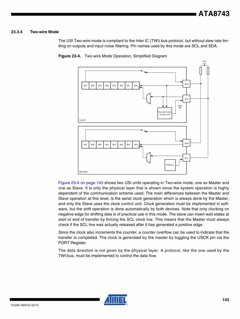
ATA8743
23.3.4 Two-wire Mode
The USI Two-wire mode is compliant to the Inter IC (TWI) bus protocol, but without slew rate lim-iting on outputs and input noise filtering. Pin names used by this mode are SCL and SDA.
Figure 23-4. Two-wire Mode Operation, Simplified Diagram
Figure 23-4 on page 143 shows two USI units operating in Two-wire mode, one as Master andone as Slave. It is only the physical layer that is shown since the system operation is highlydependent of the communication scheme used. The main differences between the Master andSlave operation at this level, is the serial clock generation which is always done by the Master,and only the Slave uses the clock control unit. Clock generation must be implemented in soft-ware, but the shift operation is done automatically by both devices. Note that only clocking onnegative edge for shifting data is of practical use in this mode. The slave can insert wait states atstart or end of transfer by forcing the SCL clock low. This means that the Master must alwayscheck if the SCL line was actually released after it has generated a positive edge.
Since the clock also increments the counter, a counter overflow can be used to indicate that thetransfer is completed. The clock is generated by the master by toggling the USCK pin via thePORT Register.
The data direction is not given by the physical layer. A protocol, like the one used by theTWI-bus, must be implemented to control the data flow.
MASTER
SLAVE
Bit7 Bit6 Bit5 Bit4 Bit3 Bit2 Bit1 Bit0 SDA
SCL
Bit7 Bit6 Bit5 Bit4 Bit3 Bit2 Bit1 Bit0
Two-wire ClockControl Unit
HOLDSCL
PORTxn
SDA
SCL
VCC
1439152B–INDCO–02/10
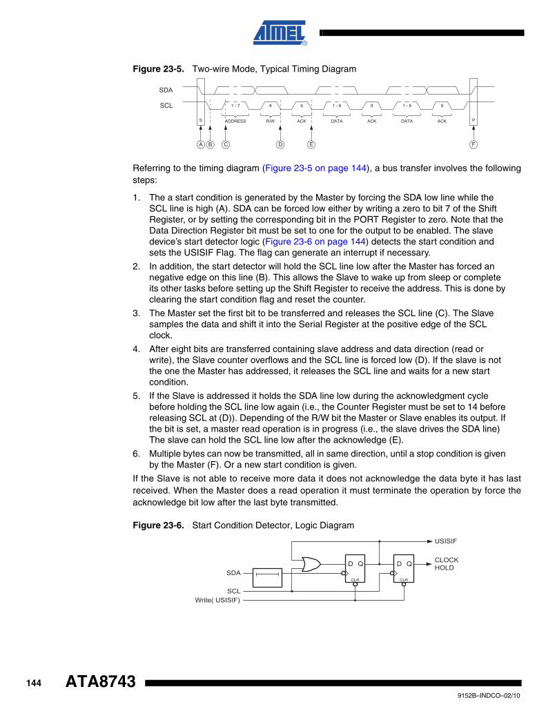
Figure 23-5. Two-wire Mode, Typical Timing Diagram
Referring to the timing diagram (Figure 23-5 on page 144), a bus transfer involves the followingsteps:
1. The a start condition is generated by the Master by forcing the SDA low line while the SCL line is high (A). SDA can be forced low either by writing a zero to bit 7 of the Shift Register, or by setting the corresponding bit in the PORT Register to zero. Note that the Data Direction Register bit must be set to one for the output to be enabled. The slave device’s start detector logic (Figure 23-6 on page 144) detects the start condition and sets the USISIF Flag. The flag can generate an interrupt if necessary.
2. In addition, the start detector will hold the SCL line low after the Master has forced an negative edge on this line (B). This allows the Slave to wake up from sleep or complete its other tasks before setting up the Shift Register to receive the address. This is done by clearing the start condition flag and reset the counter.
3. The Master set the first bit to be transferred and releases the SCL line (C). The Slave samples the data and shift it into the Serial Register at the positive edge of the SCL clock.
4. After eight bits are transferred containing slave address and data direction (read or write), the Slave counter overflows and the SCL line is forced low (D). If the slave is not the one the Master has addressed, it releases the SCL line and waits for a new start condition.
5. If the Slave is addressed it holds the SDA line low during the acknowledgment cycle before holding the SCL line low again (i.e., the Counter Register must be set to 14 before releasing SCL at (D)). Depending of the R/W bit the Master or Slave enables its output. If the bit is set, a master read operation is in progress (i.e., the slave drives the SDA line) The slave can hold the SCL line low after the acknowledge (E).
6. Multiple bytes can now be transmitted, all in same direction, until a stop condition is given by the Master (F). Or a new start condition is given.
If the Slave is not able to receive more data it does not acknowledge the data byte it has lastreceived. When the Master does a read operation it must terminate the operation by force theacknowledge bit low after the last byte transmitted.
Figure 23-6. Start Condition Detector, Logic Diagram
PS ADDRESS
1 - 7 8 9
R/W ACK ACK
1 - 8 9
DATA ACK
1 - 8 9
DATA
SDA
SCL
A B D EC F
SDA
SCLWrite( USISIF)
CLOCKHOLD
USISIF
D Q
CLR
D Q
CLR
1449152B–INDCO–02/10
ATA8743
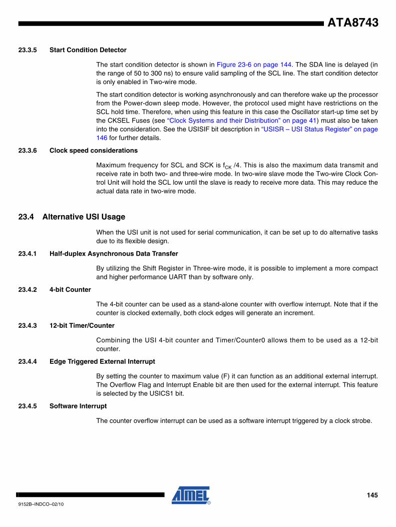
ATA8743
23.3.5 Start Condition Detector
The start condition detector is shown in Figure 23-6 on page 144. The SDA line is delayed (inthe range of 50 to 300 ns) to ensure valid sampling of the SCL line. The start condition detectoris only enabled in Two-wire mode.
The start condition detector is working asynchronously and can therefore wake up the processorfrom the Power-down sleep mode. However, the protocol used might have restrictions on theSCL hold time. Therefore, when using this feature in this case the Oscillator start-up time set bythe CKSEL Fuses (see “Clock Systems and their Distribution” on page 41) must also be takeninto the consideration. See the USISIF bit description in “USISR – USI Status Register” on page146 for further details.
23.3.6 Clock speed considerations
Maximum frequency for SCL and SCK is fCK /4. This is also the maximum data transmit andreceive rate in both two- and three-wire mode. In two-wire slave mode the Two-wire Clock Con-trol Unit will hold the SCL low until the slave is ready to receive more data. This may reduce theactual data rate in two-wire mode.
23.4 Alternative USI Usage
When the USI unit is not used for serial communication, it can be set up to do alternative tasksdue to its flexible design.
23.4.1 Half-duplex Asynchronous Data Transfer
By utilizing the Shift Register in Three-wire mode, it is possible to implement a more compactand higher performance UART than by software only.
23.4.2 4-bit Counter
The 4-bit counter can be used as a stand-alone counter with overflow interrupt. Note that if thecounter is clocked externally, both clock edges will generate an increment.
23.4.3 12-bit Timer/Counter
Combining the USI 4-bit counter and Timer/Counter0 allows them to be used as a 12-bitcounter.
23.4.4 Edge Triggered External Interrupt
By setting the counter to maximum value (F) it can function as an additional external interrupt.The Overflow Flag and Interrupt Enable bit are then used for the external interrupt. This featureis selected by the USICS1 bit.
23.4.5 Software Interrupt
The counter overflow interrupt can be used as a software interrupt triggered by a clock strobe.
1459152B–INDCO–02/10
23.5 Register Descriptions
23.5.1 USIBR – USI Data Buffer
23.5.2 USIDR – USI Data Register
The USI uses no buffering of the Serial Register, i.e., when accessing the Data Register(USIDR) the Serial Register is accessed directly. If a serial clock occurs at the same cycle theregister is written, the register will contain the value written and no shift is performed. A (left) shiftoperation is performed depending of the USICS1..0 bits setting. The shift operation can be con-trolled by an external clock edge, by a Timer/Counter0 Compare Match, or directly by softwareusing the USICLK strobe bit. Note that even when no wire mode is selected (USIWM1..0 = 0)both the external data input (DI/SDA) and the external clock input (USCK/SCL) can still be usedby the Shift Register.
The output pin in use, DO or SDA depending on the wire mode, is connected via the output latchto the most significant bit (bit 7) of the Data Register. The output latch is open (transparent) dur-ing the first half of a serial clock cycle when an external clock source is selected (USICS1 = 1),and constantly open when an internal clock source is used (USICS1 = 0). The output will bechanged immediately when a new MSB written as long as the latch is open. The latch ensuresthat data input is sampled and data output is changed on opposite clock edges.
Note that the corresponding Data Direction Register to the pin must be set to one for enablingdata output from the Shift Register.
23.5.3 USISR – USI Status Register
The Status Register contains Interrupt Flags, line Status Flags and the counter value.
• Bit 7 – USISIF: Start Condition Interrupt FlagWhen Two-wire mode is selected, the USISIF Flag is set (to one) when a start condition isdetected. When output disable mode or Three-wire mode is selected and (USICSx = 0b11 &USICLK = 0) or (USICS = 0b10 & USICLK = 0), any edge on the SCK pin sets the flag.
Bit 7 6 5 4 3 2 1 0
0x10 (0x30) MSB LSB USIBR
Read/Write R R R R R R R R
Initial Value 0 0 0 0 0 0 0 0
Bit 7 6 5 4 3 2 1 0
0x0F (0x2F) MSB LSB USIDR
Read/Write R/W R/W R/W R/W R/W R/W R/W R/W
Initial Value 0 0 0 0 0 0 0 0
Bit 7 6 5 4 3 2 1 0
0x0E (0x2E) USISIF USIOIF USIPF USIDC USICNT3 USICNT2 USICNT1 USICNT0 USISR
Read/Write R/W R/W R/W R R/W R/W R/W R/W
Initial Value 0 0 0 0 0 0 0 0
1469152B–INDCO–02/10
ATA8743
ATA8743
An interrupt will be generated when the flag is set while the USISIE bit in USICR and the GlobalInterrupt Enable Flag are set. The flag will only be cleared by writing a logical one to the USISIFbit. Clearing this bit will release the start detection hold of USCL in Two-wire mode.
A start condition interrupt will wake up the processor from all sleep modes.
• Bit 6 – USIOIF: Counter Overflow Interrupt FlagThis flag is set (one) when the 4-bit counter overflows (i.e., at the transition from 15 to 0). Aninterrupt will be generated when the flag is set while the USIOIE bit in USICR and the GlobalInterrupt Enable Flag are set. The flag is cleared if a one is written to the USIOIF bit or by read-ing the USIBR register. Clearing this bit will release the counter overflow hold of SCL inTwo-wire mode.
A counter overflow interrupt will wake up the processor from Idle sleep mode.
• Bit 5 – USIPF: Stop Condition FlagWhen Two-wire mode is selected, the USIPF Flag is set (one) when a stop condition is detected.The flag is cleared by writing a one to this bit. Note that this is not an Interrupt Flag. This signal isuseful when implementing Two-wire bus master arbitration.
• Bit 4 – USIDC: Data Output CollisionThis bit is logical one when bit 7 in the Shift Register differs from the physical pin value. The flagis only valid when Two-wire mode is used. This signal is useful when implementing Two-wirebus master arbitration.
• Bits 3..0 – USICNT3..0: Counter ValueThese bits reflect the current 4-bit counter value. The 4-bit counter value can directly be read orwritten by the CPU.
The 4-bit counter increments by one for each clock generated either by the external clock edgedetector, by a Timer/Counter0 Compare Match, or by software using USICLK or USITC strobebits. The clock source depends of the setting of the USICS1..0 bits. For external clock operationa special feature is added that allows the clock to be generated by writing to the USITC strobebit. This feature is enabled by write a one to the USICLK bit while setting an external clocksource (USICS1 = 1).
Note that even when no wire mode is selected (USIWM1..0 = 0) the external clock input(USCK/SCL) are can still be used by the counter.
23.5.4 USICR – USI Control Register
The Control Register includes interrupt enable control, wire mode setting, Clock Select setting,and clock strobe.
• Bit 7 – USISIE: Start Condition Interrupt EnableSetting this bit to one enables the Start Condition detector interrupt. If there is a pending inter-rupt when the USISIE and the Global Interrupt Enable Flag is set to one, this will immediately be
Bit 7 6 5 4 3 2 1 0
0x0D (0x2D) USISIE USIOIE USIWM1 USIWM0 USICS1 USICS0 USICLK USITC USICR
Read/Write R/W R/W R/W R/W R/W R/W W W
Initial Value 0 0 0 0 0 0 0 0
1479152B–INDCO–02/10
executed. See the USISIF bit description in “USISR – USI Status Register” on page 146 for fur-ther details.
• Bit 6 – USIOIE: Counter Overflow Interrupt EnableSetting this bit to one enables the Counter Overflow interrupt. If there is a pending interrupt whenthe USIOIE and the Global Interrupt Enable Flag is set to one, this will immediately be executed.See the USIOIF bit description in “USISR – USI Status Register” on page 146 for further details.
• Bit 5..4 – USIWM1..0: Wire ModeThese bits set the type of wire mode to be used. Basically only the function of the outputs areaffected by these bits. Data and clock inputs are not affected by the mode selected and willalways have the same function. The counter and Shift Register can therefore be clocked exter-nally, and data input sampled, even when outputs are disabled. The relations betweenUSIWM1..0 and the USI operation is summarized in Table 23-1.
Note: 1. The DI and USCK pins are renamed to Serial Data (SDA) and Serial Clock (SCL) respectively to avoid confusion between the modes of operation.
Table 23-1. Relations between USIWM1..0 and the USI Operation
USIWM1 USIWM0 Description
0 0Outputs, clock hold, and start detector disabled. Port pins operates as normal.
0 1
Three-wire mode. Uses DO, DI, and USCK pins.
The Data Output (DO) pin overrides the corresponding bit in the PORT Register in this mode. However, the corresponding DDR bit still controls the data direction. When the port pin is set as input the pins pull-up is controlled by the PORT bit.
The Data Input (DI) and Serial Clock (USCK) pins do not affect the normal port operation. When operating as master, clock pulses are software generated by toggling the PORT Register, while the data direction is set to output. The USITC bit in the USICR Register can be used for this purpose.
1 0
Two-wire mode. Uses SDA (DI) and SCL (USCK) pins(1).
The Serial Data (SDA) and the Serial Clock (SCL) pins are bi-directional and uses open-collector output drives. The output drivers are enabled by setting the corresponding bit for SDA and SCL in the DDR Register.When the output driver is enabled for the SDA pin, the output driver will force the line SDA low if the output of the Shift Register or the corresponding bit in the PORT Register is zero. Otherwise the SDA line will not be driven (i.e., it is released). When the SCL pin output driver is enabled the SCL line will be forced low if the corresponding bit in the PORT Register is zero, or by the start detector. Otherwise the SCL line will not be driven.
The SCL line is held low when a start detector detects a start condition and the output is enabled. Clearing the Start Condition Flag (USISIF) releases the line. The SDA and SCL pin inputs is not affected by enabling this mode. Pull-ups on the SDA and SCL port pin are disabled in Two-wire mode.
1 1
Two-wire mode. Uses SDA and SCL pins.
Same operation as for the Two-wire mode described above, except that the SCL line is also held low when a counter overflow occurs, and is held low until the Counter Overflow Flag (USIOIF) is cleared.
1489152B–INDCO–02/10
ATA8743
ATA8743
• Bit 3..2 – USICS1..0: Clock Source Select
These bits set the clock source for the Shift Register and counter. The data output latch ensuresthat the output is changed at the opposite edge of the sampling of the data input (DI/SDA) whenusing external clock source (USCK/SCL). When software strobe or Timer/Counter0 CompareMatch clock option is selected, the output latch is transparent and therefore the output ischanged immediately. Clearing the USICS1..0 bits enables software strobe option. When usingthis option, writing a one to the USICLK bit clocks both the Shift Register and the counter. Forexternal clock source (USICS1 = 1), the USICLK bit is no longer used as a strobe, but selectsbetween external clocking and software clocking by the USITC strobe bit.
Table 23-2 on page 149 shows the relationship between the USICS1..0 and USICLK setting andclock source used for the Shift Register and the 4-bit counter.
• Bit 1 – USICLK: Clock StrobeWriting a one to this bit location strobes the Shift Register to shift one step and the counter toincrement by one, provided that the USICS1..0 bits are set to zero and by doing so the softwareclock strobe option is selected. The output will change immediately when the clock strobe is exe-cuted, i.e., in the same instruction cycle. The value shifted into the Shift Register is sampled theprevious instruction cycle. The bit will be read as zero.
When an external clock source is selected (USICS1 = 1), the USICLK function is changed froma clock strobe to a Clock Select Register. Setting the USICLK bit in this case will select theUSITC strobe bit as clock source for the 4-bit counter (see Table 23-2 on page 149).
• Bit 0 – USITC: Toggle Clock Port PinWriting a one to this bit location toggles the USCK/SCL value either from 0 to 1, or from 1 to 0.The toggling is independent of the setting in the Data Direction Register, but if the PORT value isto be shown on the pin the DDRE4 must be set as output (to one). This feature allows easy clockgeneration when implementing master devices. The bit will be read as zero.
When an external clock source is selected (USICS1 = 1) and the USICLK bit is set to one, writ-ing to the USITC strobe bit will directly clock the 4-bit counter. This allows an early detection ofwhen the transfer is done when operating as a master device.
Table 23-2. Relations between the USICS1..0 and USICLK Setting
USICS1 USICS0 USICLK Shift Register Clock Source 4-bit Counter Clock Source
0 0 0 No Clock No Clock
0 0 1Software clock strobe (USICLK)
Software clock strobe (USICLK)
0 1 XTimer/Counter0 Compare Match
Timer/Counter0 Compare Match
1 0 0 External, positive edge External, both edges
1 1 0 External, negative edge External, both edges
1 0 1 External, positive edge Software clock strobe (USITC)
1 1 1 External, negative edge Software clock strobe (USITC)
1499152B–INDCO–02/10
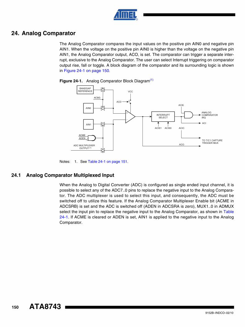
24. Analog Comparator
The Analog Comparator compares the input values on the positive pin AIN0 and negative pinAIN1. When the voltage on the positive pin AIN0 is higher than the voltage on the negative pinAIN1, the Analog Comparator output, ACO, is set. The comparator can trigger a separate inter-rupt, exclusive to the Analog Comparator. The user can select Interrupt triggering on comparatoroutput rise, fall or toggle. A block diagram of the comparator and its surrounding logic is shownin Figure 24-1 on page 150.
Figure 24-1. Analog Comparator Block Diagram(1)
Notes: 1. See Table 24-1 on page 151.
24.1 Analog Comparator Multiplexed Input
When the Analog to Digital Converter (ADC) is configured as single ended input channel, it ispossible to select any of the ADC7..0 pins to replace the negative input to the Analog Compara-tor. The ADC multiplexer is used to select this input, and consequently, the ADC must beswitched off to utilize this feature. If the Analog Comparator Multiplexer Enable bit (ACME inADCSRB) is set and the ADC is switched off (ADEN in ADCSRA is zero), MUX1..0 in ADMUXselect the input pin to replace the negative input to the Analog Comparator, as shown in Table24-1. If ACME is cleared or ADEN is set, AIN1 is applied to the negative input to the AnalogComparator.
ACBG
BANDGAPREFERENCE
ADC MULTIPLEXEROUTPUT
ACMEADEN
(1)
1509152B–INDCO–02/10
ATA8743
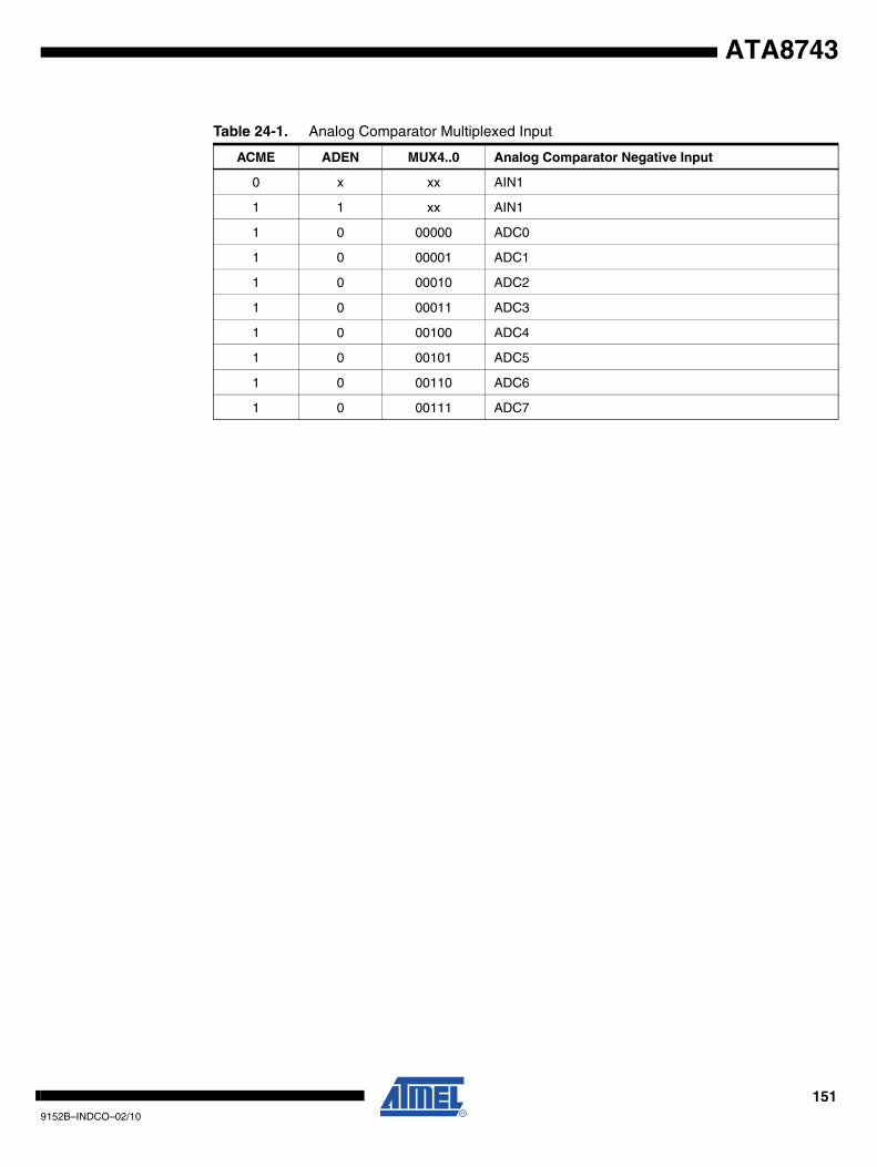
ATA8743
Table 24-1. Analog Comparator Multiplexed Input
ACME ADEN MUX4..0 Analog Comparator Negative Input
0 x xx AIN1
1 1 xx AIN1
1 0 00000 ADC0
1 0 00001 ADC1
1 0 00010 ADC2
1 0 00011 ADC3
1 0 00100 ADC4
1 0 00101 ADC5
1 0 00110 ADC6
1 0 00111 ADC7
1519152B–INDCO–02/10
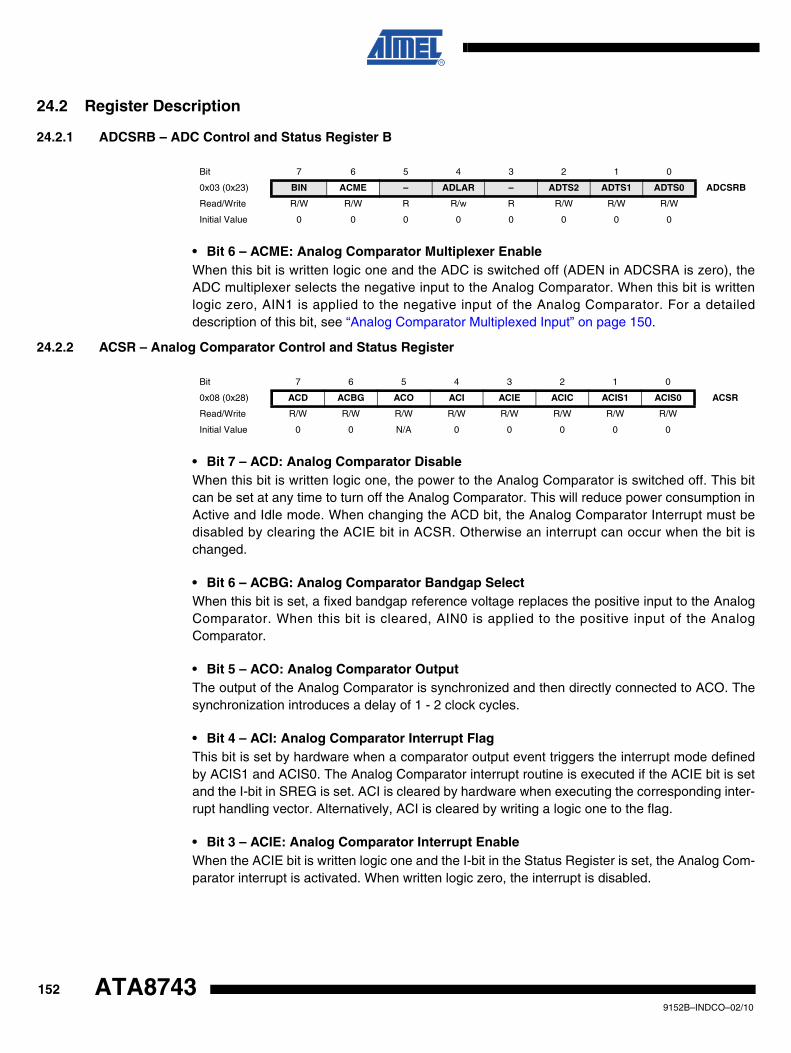
24.2 Register Description
24.2.1 ADCSRB – ADC Control and Status Register B
• Bit 6 – ACME: Analog Comparator Multiplexer EnableWhen this bit is written logic one and the ADC is switched off (ADEN in ADCSRA is zero), theADC multiplexer selects the negative input to the Analog Comparator. When this bit is writtenlogic zero, AIN1 is applied to the negative input of the Analog Comparator. For a detaileddescription of this bit, see “Analog Comparator Multiplexed Input” on page 150.
24.2.2 ACSR – Analog Comparator Control and Status Register
• Bit 7 – ACD: Analog Comparator DisableWhen this bit is written logic one, the power to the Analog Comparator is switched off. This bitcan be set at any time to turn off the Analog Comparator. This will reduce power consumption inActive and Idle mode. When changing the ACD bit, the Analog Comparator Interrupt must bedisabled by clearing the ACIE bit in ACSR. Otherwise an interrupt can occur when the bit ischanged.
• Bit 6 – ACBG: Analog Comparator Bandgap SelectWhen this bit is set, a fixed bandgap reference voltage replaces the positive input to the AnalogComparator. When this bit is cleared, AIN0 is applied to the positive input of the AnalogComparator.
• Bit 5 – ACO: Analog Comparator OutputThe output of the Analog Comparator is synchronized and then directly connected to ACO. Thesynchronization introduces a delay of 1 - 2 clock cycles.
• Bit 4 – ACI: Analog Comparator Interrupt FlagThis bit is set by hardware when a comparator output event triggers the interrupt mode definedby ACIS1 and ACIS0. The Analog Comparator interrupt routine is executed if the ACIE bit is setand the I-bit in SREG is set. ACI is cleared by hardware when executing the corresponding inter-rupt handling vector. Alternatively, ACI is cleared by writing a logic one to the flag.
• Bit 3 – ACIE: Analog Comparator Interrupt EnableWhen the ACIE bit is written logic one and the I-bit in the Status Register is set, the Analog Com-parator interrupt is activated. When written logic zero, the interrupt is disabled.
Bit 7 6 5 4 3 2 1 0
0x03 (0x23) BIN ACME – ADLAR – ADTS2 ADTS1 ADTS0 ADCSRB
Read/Write R/W R/W R R/w R R/W R/W R/W
Initial Value 0 0 0 0 0 0 0 0
Bit 7 6 5 4 3 2 1 0
0x08 (0x28) ACD ACBG ACO ACI ACIE ACIC ACIS1 ACIS0 ACSR
Read/Write R/W R/W R/W R/W R/W R/W R/W R/W
Initial Value 0 0 N/A 0 0 0 0 0
1529152B–INDCO–02/10
ATA8743
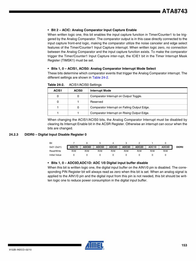
ATA8743
• Bit 2 – ACIC: Analog Comparator Input Capture Enable When written logic one, this bit enables the input capture function in Timer/Counter1 to be trig-gered by the Analog Comparator. The comparator output is in this case directly connected to theinput capture front-end logic, making the comparator utilize the noise canceler and edge selectfeatures of the Timer/Counter1 Input Capture interrupt. When written logic zero, no connectionbetween the Analog Comparator and the input capture function exists. To make the comparatortrigger the Timer/Counter1 Input Capture inter-rupt, the ICIE1 bit in the Timer Interrupt MaskRegister (TIMSK1) must be set.
• Bits 1, 0 – ACIS1, ACIS0: Analog Comparator Interrupt Mode SelectThese bits determine which comparator events that trigger the Analog Comparator interrupt. Thedifferent settings are shown in Table 24-2.
When changing the ACIS1/ACIS0 bits, the Analog Comparator Interrupt must be disabled byclearing its Interrupt Enable bit in the ACSR Register. Otherwise an interrupt can occur when thebits are changed.
24.2.3 DIDR0 – Digital Input Disable Register 0
• Bits 1, 0 – ADC0D,ADC1D: ADC 1/0 Digital input buffer disableWhen this bit is written logic one, the digital input buffer on the AIN1/0 pin is disabled. The corre-sponding PIN Register bit will always read as zero when this bit is set. When an analog signal isapplied to the AIN1/0 pin and the digital input from this pin is not needed, this bit should be writ-ten logic one to reduce power consumption in the digital input buffer.
Table 24-2. ACIS1/ACIS0 Settings
ACIS1 ACIS0 Interrupt Mode
0 0 Comparator Interrupt on Output Toggle.
0 1 Reserved
1 0 Comparator Interrupt on Falling Output Edge.
1 1 Comparator Interrupt on Rising Output Edge.
Bit 7 6 5 4 3 2 1 0
0x01 (0x21) ADC7D ADC6D ADC5D ADC4D ADC3D ADC2D ADC1D ADC0D DIDR0
Read/Write R/W R/W R/W R/W R/W R/W R/W R/W
Initial Value 0 0 0 0 0 0 0 0
1539152B–INDCO–02/10
25. Analog to Digital Converter
25.1 Features
• 10-bit Resolution• 1.0 LSB Integral Non-linearity• ± 2 LSB Absolute Accuracy• 65 - 260 µs Conversion Time• Up to 76 kSPS at Maximum Resolution• Eight Multiplexed Single Ended Input Channels• Twelve differential input channels with selectable gain (1x, 20x)• Temperature sensor input channel• Optional Left Adjustment for ADC Result Readout• 0 - VCC ADC Input Voltage Range• 1.1V ADC Reference Voltage• Free Running or Single Conversion Mode• ADC Start Conversion by Auto Triggering on Interrupt Sources• Interrupt on ADC Conversion Complete• Sleep Mode Noise Canceler• Unipolar / Bipolar Input Mode• Input Polarity Reversal channels
25.2 Overview
The ATtiny24/44/84 features a 10-bit successive approximation ADC. The ADC is connected to8-pin port A for external sources. In addition to external sources internal temperature sensor canbe measured by ADC. Analog Multiplexer allows eight single-ended channels or 12 differentialchannels from Port A. The programmable gain stage provides amplification steps 0 dB (1x) and26 dB (20x) for 12 differential ADC channels.
The ADC contains a Sample and Hold circuit which ensures that the input voltage to the ADC isheld at a constant level during conversion. A block diagram of the ADC is shown in Figure 25-1on page 155.
Internal reference voltage of nominally 1.1V is provided On-chip. Alternatively, VCC can be usedas reference voltage for single ended channels. There is also an option to use an external volt-age reference and turn-off the internal voltage reference.
1549152B–INDCO–02/10
ATA8743
ATA8743
Figure 25-1. Analog to Digital Converter Block Schematic
25.3 ADC Operation
The ADC converts an analog input voltage to a 10-bit digital value through successive approxi-mation. The minimum value represents GND and the maximum value represents the referencevoltage.The voltage reference for the ADC may be selected by writing to the REFS1..0 bits inADMUX. The VCC supply, the AREF pin or an internal 1.1V voltage reference may be selectedas the ADC voltage reference.
The analog input channel and differential gain are selected by writing to the MUX5..0 bits inADMUX. Any of the eight ADC input pins ADC7..0 can be selected as single ended inputs to theADC. For differential measurements all analog inputs next to each other can be selected as ainput pair. Every input is also possible to measure with ADC3. These pairs of differential inputsare measured by ADC trough the differential gain amplifier.
If differential channels are selected, the differential gain stage amplifies the voltage differencebetween the selected input pair by the selected gain factor, 1x or 20x, according to the setting of
ADC CONVERSIONCOMPLETE IRQ
8-BIT DATA BUS
15 0
ADC MULTIPLEXERSELECT (ADMUX)
ADC CTRL. & STATUS AREGISTER (ADCSRA)
ADC DATA REGISTER(ADCH/ADCL)
AD
IE
AD
AT
E
AD
SC
AD
EN
AD
IFA
DIF
MU
X4.
..MU
X0
AD
PS
0
AD
PS
1
AD
PS
2
CONVERSION LOGIC
10-BIT DAC
+-
SAMPLE & HOLDCOMPARATOR
INTERNAL REFERENCE
1.1V
MUX DECODER
VCC
ADC7
ADC6
ADC5
ADC4
RE
FS
1..R
EF
S0
AD
LAR
CH
AN
NE
L S
ELE
CT
ION
AD
C[9
:0]
ADC MULTIPLEXEROUTPUT
PRESCALER
TRIGGERSELECT
ADTS2...ADTS0
INTERRUPTFLAGS
START
+
-
GA
IN S
ELE
CT
ION
GAINAMPLIFIER
NEG.INPUTMUX
SINGLE ENDED / DIFFERENTIAL SELECTION
TEMPERATURE SENSOR
ADC8
BIN
IPR
ADC3
ADC2
ADC1
ADC0
POS.INPUTMUX
AGND
ADC CTRL. & STATUS BREGISTER (ADCSRB)
AREF
1559152B–INDCO–02/10
the MUX0 bit in ADMUX. This amplified value then becomes the analog input to the ADC. If sin-gle ended channels are used, the gain amplifier is bypassed altogether.
The offset of the differential channels can be measure by selecting the same input for both neg-ative and positive input. Offset calibration can be done for ADC0, ADC3 and ADC7. When ADC0or ADC3 or ADC7 is selected as both the positive and negative input to the differential gainamplifier, the remaining offset in the gain stage and conversion circuitry can be measureddirectly as the result of the conversion. This figure can be subtracted from subsequent conver-sions with the same gain setting to reduce offset error to below 1 LSB.
The on-chip temperature sensor is selected by writing the code “100010” to the MUX5..0 bits inADMUX register.
The ADC is enabled by setting the ADC Enable bit, ADEN in ADCSRA. Voltage reference andinput channel selections will not go into effect until ADEN is set. The ADC does not consumepower when ADEN is cleared, so it is recommended to switch off the ADC before entering powersaving sleep modes.
The ADC generates a 10-bit result which is presented in the ADC Data Registers, ADCH andADCL. By default, the result is presented right adjusted, but can optionally be presented leftadjusted by setting the ADLAR bit in ADCSRB.
If the result is left adjusted and no more than 8-bit precision is required, it is sufficient to readADCH. Otherwise, ADCL must be read first, then ADCH, to ensure that the content of the dataregisters belongs to the same conversion. Once ADCL is read, ADC access to data registers isblocked. This means that if ADCL has been read, and a conversion completes before ADCH isread, neither register is updated and the result from the conversion is lost. When ADCH is read,ADC access to the ADCH and ADCL Registers is re-enabled.
The ADC has its own interrupt which can be triggered when a conversion completes. When ADCaccess to the data registers is prohibited between reading of ADCH and ADCL, the interrupt willtrigger even if the result is lost.
25.4 Starting a Conversion
A single conversion is started by writing a logical one to the ADC Start Conversion bit, ADSC.This bit stays high as long as the conversion is in progress and will be cleared by hardwarewhen the conversion is completed. If a different data channel is selected while a conversion is inprogress, the ADC will finish the current conversion before performing the channel change.
Alternatively, a conversion can be triggered automatically by various sources. Auto Triggering isenabled by setting the ADC Auto Trigger Enable bit, ADATE in ADCSRA. The trigger source isselected by setting the ADC Trigger Select bits, ADTS in ADCSRB (see description of the ADTSbits for a list of the trigger sources). When a positive edge occurs on the selected trigger signal,the ADC prescaler is reset and a conversion is started. This provides a method of starting con-versions at fixed intervals. If the trigger signal still is set when the conversion completes, a newconversion will not be started. If another positive edge occurs on the trigger signal during con-version, the edge will be ignored. Note that an Interrupt Flag will be set even if the specificinterrupt is disabled or the Global Interrupt Enable bit in SREG is cleared. A conversion can thusbe triggered without causing an interrupt. However, the Interrupt Flag must be cleared in order totrigger a new conversion at the next interrupt event.
1569152B–INDCO–02/10
ATA8743
ATA8743
Figure 25-2. ADC Auto Trigger Logic
Using the ADC Interrupt Flag as a trigger source makes the ADC start a new conversion as soonas the ongoing conversion has finished. The ADC then operates in Free Running mode, con-stantly sampling and updating the ADC Data Register. The first conversion must be started bywriting a logical one to the ADSC bit in ADCSRA. In this mode the ADC will perform successiveconversions independently of whether the ADC Interrupt Flag, ADIF is cleared or not.
If Auto Triggering is enabled, single conversions can be started by writing ADSC in ADCSRA toone. ADSC can also be used to determine if a conversion is in progress. The ADSC bit will beread as one during a conversion, independently of how the conversion was started.
25.5 Prescaling and Conversion Timing
Figure 25-3. ADC Prescaler
By default, the successive approximation circuitry requires an input clock frequency between 50kHz and 200 kHz to get maximum resolution. If a lower resolution than 10 bits is needed, theinput clock frequency to the ADC can be higher than 200 kHz to get a higher sample rate.
The ADC module contains a prescaler, which generates an acceptable ADC clock frequencyfrom any CPU frequency above 100 kHz. The prescaling is set by the ADPS bits in ADCSRA.
ADSC
ADIF
SOURCE 1
SOURCE n
ADTS[2:0]
CONVERSIONLOGIC
PRESCALER
START CLKADC
.
.
.
. EDGEDETECTOR
ADATE
7-BIT ADC PRESCALER
ADC CLOCK SOURCE
CK
ADPS0ADPS1ADPS2
CK
/128
CK
/2
CK
/4
CK
/8
CK
/16
CK
/32
CK
/64
ResetADENSTART
1579152B–INDCO–02/10
The prescaler starts counting from the moment the ADC is switched on by setting the ADEN bitin ADCSRA. The prescaler keeps running for as long as the ADEN bit is set, and is continuouslyreset when ADEN is low.
When initiating a single ended conversion by setting the ADSC bit in ADCSRA, the conversionstarts at the following rising edge of the ADC clock cycle.
A normal conversion takes 13 ADC clock cycles. The first conversion after the ADC is switchedon (ADEN in ADCSRA is set) takes 25 ADC clock cycles in order to initialize the analog circuitry.
The actual sample-and-hold takes place 1.5 ADC clock cycles after the start of a normal conver-sion and 14.5 ADC clock cycles after the start of an first conversion. When a conversion iscomplete, the result is written to the ADC Data Registers, and ADIF is set. In Single Conversionmode, ADSC is cleared simultaneously. The software may then set ADSC again, and a newconversion will be initiated on the first rising ADC clock edge.
When Auto Triggering is used, the prescaler is reset when the trigger event occurs. This assuresa fixed delay from the trigger event to the start of conversion. In this mode, the sample-and-holdtakes place two ADC clock cycles after the rising edge on the trigger source signal. Three addi-tional CPU clock cycles are used for synchronization logic.
In Free Running mode, a new conversion will be started immediately after the conversion com-pletes, while ADSC remains high. For a summary of conversion times, see Table 25-1 on page159.
Figure 25-4. ADC Timing Diagram, First Conversion (Single Conversion Mode)
Figure 25-5. ADC Timing Diagram, Single Conversion
Sign and MSB of Result
LSB of Result
ADC Clock
ADSC
Sample & Hold
ADIF
ADCH
ADCL
Cycle Number
ADEN
1 2 12 13 14 15 16 17 18 19 20 21 22 23 24 25 1 2
First ConversionNextConversion
3
MUX and REFSUpdate
MUX and REFSUpdate
ConversionComplete
1 2 3 4 5 6 7 8 9 10 11 12 13
Sign and MSB of Result
LSB of Result
ADC Clock
ADSC
ADIF
ADCH
ADCL
Cycle Number 1 2
One Conversion Next Conversion
3
Sample & Hold
MUX and REFSUpdate
ConversionComplete
MUX and REFSUpdate
1589152B–INDCO–02/10
ATA8743
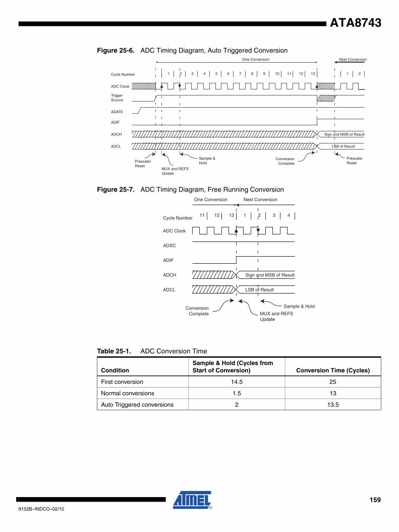
ATA8743
Figure 25-6. ADC Timing Diagram, Auto Triggered Conversion
Figure 25-7. ADC Timing Diagram, Free Running Conversion
Table 25-1. ADC Conversion Time
ConditionSample & Hold (Cycles from Start of Conversion) Conversion Time (Cycles)
First conversion 14.5 25
Normal conversions 1.5 13
Auto Triggered conversions 2 13.5
1 2 3 4 5 6 7 8 9 10 11 12 13
Sign and MSB of Result
LSB of Result
ADC Clock
TriggerSource
ADIF
ADCH
ADCL
Cycle Number 1 2
One Conversion Next Conversion
ConversionCompletePrescaler
Reset
ADATE
PrescalerReset
Sample &Hold
MUX and REFS Update
11 12 13
Sign and MSB of Result
LSB of Result
ADC Clock
ADSC
ADIF
ADCH
ADCL
Cycle Number1 2
One Conversion Next Conversion
3 4
ConversionComplete
Sample & Hold
MUX and REFSUpdate
1599152B–INDCO–02/10
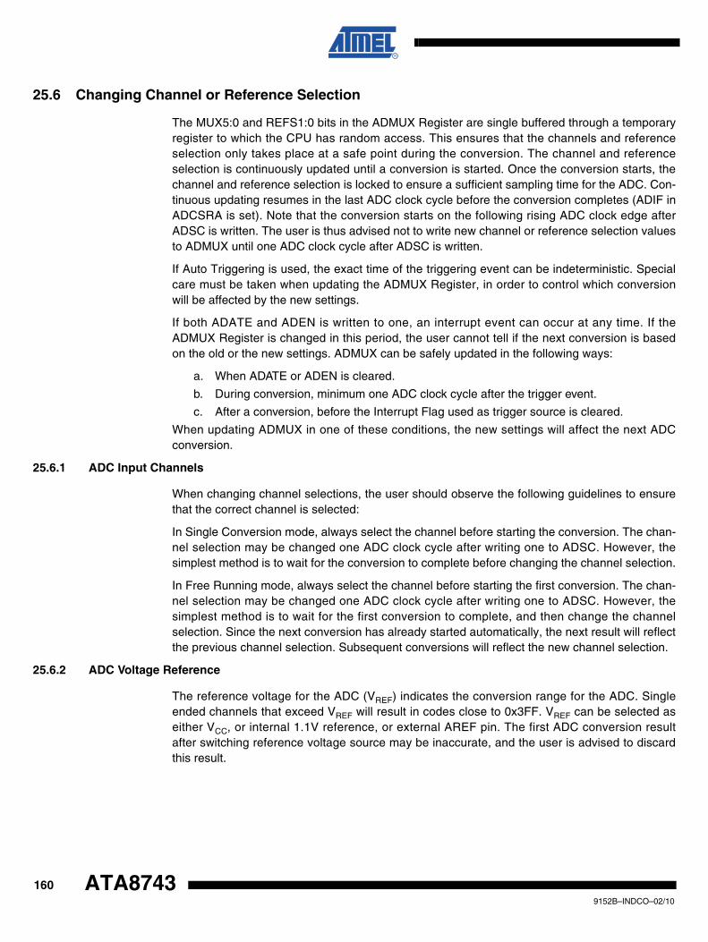
25.6 Changing Channel or Reference Selection
The MUX5:0 and REFS1:0 bits in the ADMUX Register are single buffered through a temporaryregister to which the CPU has random access. This ensures that the channels and referenceselection only takes place at a safe point during the conversion. The channel and referenceselection is continuously updated until a conversion is started. Once the conversion starts, thechannel and reference selection is locked to ensure a sufficient sampling time for the ADC. Con-tinuous updating resumes in the last ADC clock cycle before the conversion completes (ADIF inADCSRA is set). Note that the conversion starts on the following rising ADC clock edge afterADSC is written. The user is thus advised not to write new channel or reference selection valuesto ADMUX until one ADC clock cycle after ADSC is written.
If Auto Triggering is used, the exact time of the triggering event can be indeterministic. Specialcare must be taken when updating the ADMUX Register, in order to control which conversionwill be affected by the new settings.
If both ADATE and ADEN is written to one, an interrupt event can occur at any time. If theADMUX Register is changed in this period, the user cannot tell if the next conversion is basedon the old or the new settings. ADMUX can be safely updated in the following ways:
a. When ADATE or ADEN is cleared.
b. During conversion, minimum one ADC clock cycle after the trigger event.
c. After a conversion, before the Interrupt Flag used as trigger source is cleared.
When updating ADMUX in one of these conditions, the new settings will affect the next ADCconversion.
25.6.1 ADC Input Channels
When changing channel selections, the user should observe the following guidelines to ensurethat the correct channel is selected:
In Single Conversion mode, always select the channel before starting the conversion. The chan-nel selection may be changed one ADC clock cycle after writing one to ADSC. However, thesimplest method is to wait for the conversion to complete before changing the channel selection.
In Free Running mode, always select the channel before starting the first conversion. The chan-nel selection may be changed one ADC clock cycle after writing one to ADSC. However, thesimplest method is to wait for the first conversion to complete, and then change the channelselection. Since the next conversion has already started automatically, the next result will reflectthe previous channel selection. Subsequent conversions will reflect the new channel selection.
25.6.2 ADC Voltage Reference
The reference voltage for the ADC (VREF) indicates the conversion range for the ADC. Singleended channels that exceed VREF will result in codes close to 0x3FF. VREF can be selected aseither VCC, or internal 1.1V reference, or external AREF pin. The first ADC conversion resultafter switching reference voltage source may be inaccurate, and the user is advised to discardthis result.
1609152B–INDCO–02/10
ATA8743
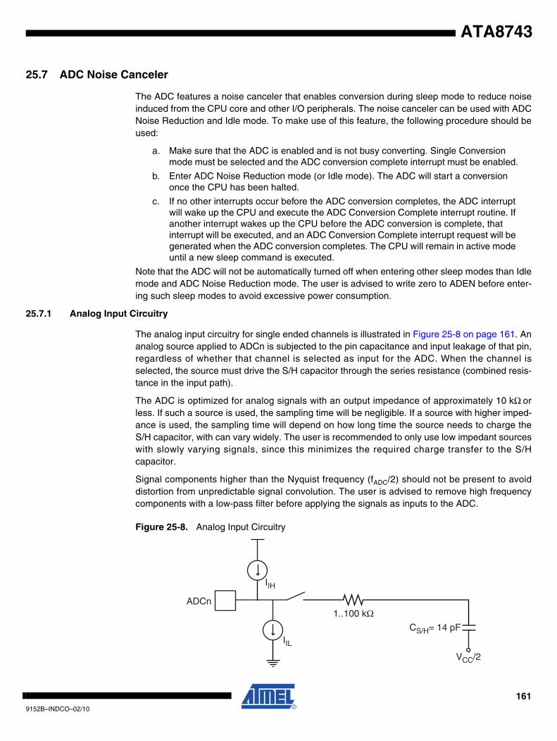
ATA8743
25.7 ADC Noise Canceler
The ADC features a noise canceler that enables conversion during sleep mode to reduce noiseinduced from the CPU core and other I/O peripherals. The noise canceler can be used with ADCNoise Reduction and Idle mode. To make use of this feature, the following procedure should beused:
a. Make sure that the ADC is enabled and is not busy converting. Single Conversion mode must be selected and the ADC conversion complete interrupt must be enabled.
b. Enter ADC Noise Reduction mode (or Idle mode). The ADC will start a conversion once the CPU has been halted.
c. If no other interrupts occur before the ADC conversion completes, the ADC interrupt will wake up the CPU and execute the ADC Conversion Complete interrupt routine. If another interrupt wakes up the CPU before the ADC conversion is complete, that interrupt will be executed, and an ADC Conversion Complete interrupt request will be generated when the ADC conversion completes. The CPU will remain in active mode until a new sleep command is executed.
Note that the ADC will not be automatically turned off when entering other sleep modes than Idlemode and ADC Noise Reduction mode. The user is advised to write zero to ADEN before enter-ing such sleep modes to avoid excessive power consumption.
25.7.1 Analog Input Circuitry
The analog input circuitry for single ended channels is illustrated in Figure 25-8 on page 161. Ananalog source applied to ADCn is subjected to the pin capacitance and input leakage of that pin,regardless of whether that channel is selected as input for the ADC. When the channel isselected, the source must drive the S/H capacitor through the series resistance (combined resis-tance in the input path).
The ADC is optimized for analog signals with an output impedance of approximately 10 kΩ orless. If such a source is used, the sampling time will be negligible. If a source with higher imped-ance is used, the sampling time will depend on how long time the source needs to charge theS/H capacitor, with can vary widely. The user is recommended to only use low impedant sourceswith slowly varying signals, since this minimizes the required charge transfer to the S/Hcapacitor.
Signal components higher than the Nyquist frequency (fADC/2) should not be present to avoiddistortion from unpredictable signal convolution. The user is advised to remove high frequencycomponents with a low-pass filter before applying the signals as inputs to the ADC.
Figure 25-8. Analog Input Circuitry
ADCn
IIH
1..100 kΩCS/H= 14 pF
VCC/2
IIL
1619152B–INDCO–02/10
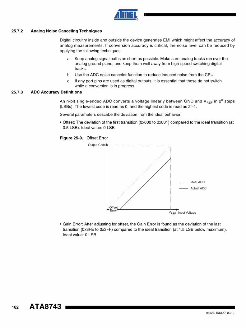
25.7.2 Analog Noise Canceling Techniques
Digital circuitry inside and outside the device generates EMI which might affect the accuracy ofanalog measurements. If conversion accuracy is critical, the noise level can be reduced byapplying the following techniques:
a. Keep analog signal paths as short as possible. Make sure analog tracks run over the analog ground plane, and keep them well away from high-speed switching digital tracks.
b. Use the ADC noise canceler function to reduce induced noise from the CPU.
c. If any port pins are used as digital outputs, it is essential that these do not switch while a conversion is in progress.
25.7.3 ADC Accuracy Definitions
An n-bit single-ended ADC converts a voltage linearly between GND and VREF in 2n steps(LSBs). The lowest code is read as 0, and the highest code is read as 2n-1.
Several parameters describe the deviation from the ideal behavior:
• Offset: The deviation of the first transition (0x000 to 0x001) compared to the ideal transition (at 0.5 LSB). Ideal value: 0 LSB.
Figure 25-9. Offset Error
• Gain Error: After adjusting for offset, the Gain Error is found as the deviation of the last transition (0x3FE to 0x3FF) compared to the ideal transition (at 1.5 LSB below maximum). Ideal value: 0 LSB
Output Code
VREF Input Voltage
Ideal ADC
Actual ADC
OffsetError
1629152B–INDCO–02/10
ATA8743
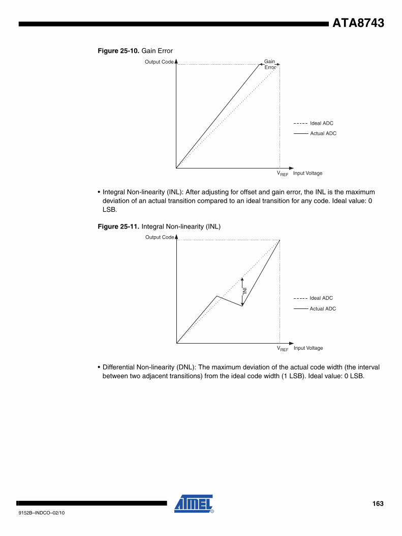
ATA8743
Figure 25-10. Gain Error
• Integral Non-linearity (INL): After adjusting for offset and gain error, the INL is the maximum deviation of an actual transition compared to an ideal transition for any code. Ideal value: 0 LSB.
Figure 25-11. Integral Non-linearity (INL)
• Differential Non-linearity (DNL): The maximum deviation of the actual code width (the interval between two adjacent transitions) from the ideal code width (1 LSB). Ideal value: 0 LSB.
Output Code
VREF Input Voltage
Ideal ADC
Actual ADC
GainError
Output Code
VREF Input Voltage
Ideal ADC
Actual ADC
INL
1639152B–INDCO–02/10
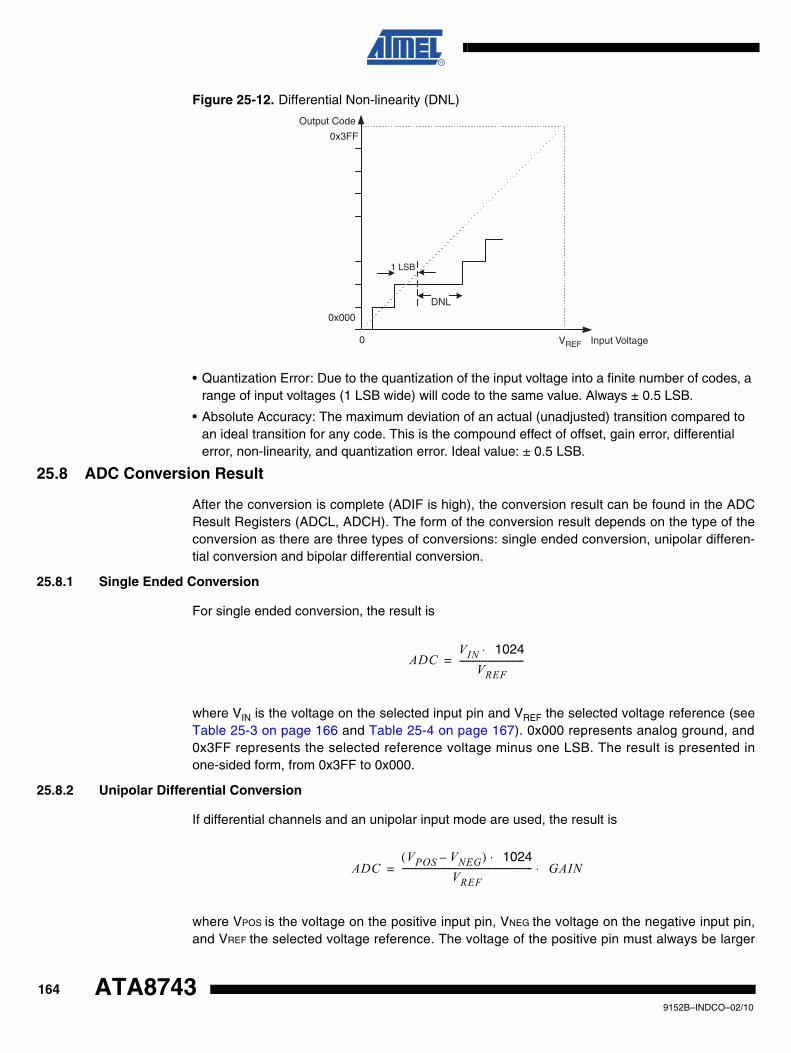
Figure 25-12. Differential Non-linearity (DNL)
• Quantization Error: Due to the quantization of the input voltage into a finite number of codes, a range of input voltages (1 LSB wide) will code to the same value. Always ± 0.5 LSB.
• Absolute Accuracy: The maximum deviation of an actual (unadjusted) transition compared to an ideal transition for any code. This is the compound effect of offset, gain error, differential error, non-linearity, and quantization error. Ideal value: ± 0.5 LSB.
25.8 ADC Conversion Result
After the conversion is complete (ADIF is high), the conversion result can be found in the ADCResult Registers (ADCL, ADCH). The form of the conversion result depends on the type of theconversion as there are three types of conversions: single ended conversion, unipolar differen-tial conversion and bipolar differential conversion.
25.8.1 Single Ended Conversion
For single ended conversion, the result is
where VIN is the voltage on the selected input pin and VREF the selected voltage reference (seeTable 25-3 on page 166 and Table 25-4 on page 167). 0x000 represents analog ground, and0x3FF represents the selected reference voltage minus one LSB. The result is presented inone-sided form, from 0x3FF to 0x000.
25.8.2 Unipolar Differential Conversion
If differential channels and an unipolar input mode are used, the result is
where VPOS is the voltage on the positive input pin, VNEG the voltage on the negative input pin,and VREF the selected voltage reference. The voltage of the positive pin must always be larger
Output Code
0x3FF
0x000
0 VREF Input Voltage
DNL
1 LSB
ADCVIN 1024⋅
VREF-----------------------------=
ADCVPOS VNEG–( ) 1024⋅
VREF----------------------------------------------------------- GAIN⋅=
1649152B–INDCO–02/10
ATA8743
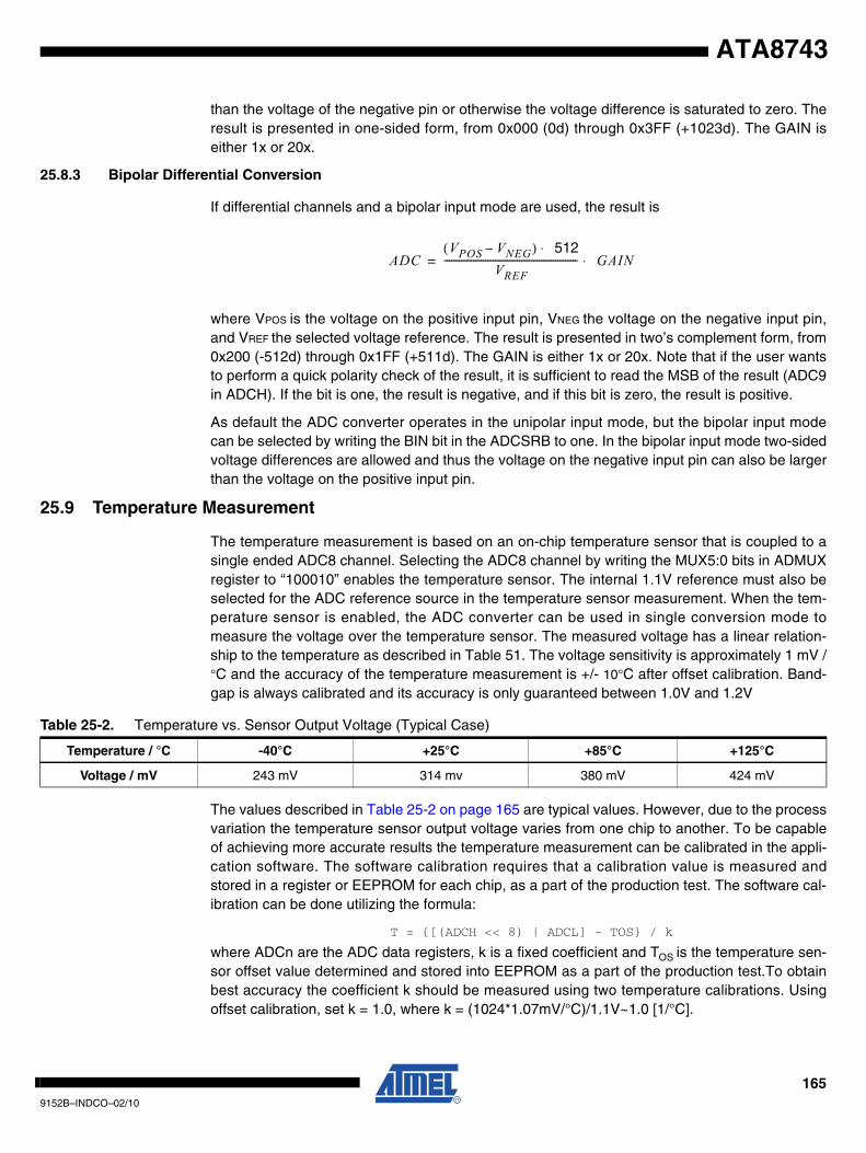
ATA8743
than the voltage of the negative pin or otherwise the voltage difference is saturated to zero. Theresult is presented in one-sided form, from 0x000 (0d) through 0x3FF (+1023d). The GAIN iseither 1x or 20x.
25.8.3 Bipolar Differential Conversion
If differential channels and a bipolar input mode are used, the result is
where VPOS is the voltage on the positive input pin, VNEG the voltage on the negative input pin,and VREF the selected voltage reference. The result is presented in two’s complement form, from0x200 (-512d) through 0x1FF (+511d). The GAIN is either 1x or 20x. Note that if the user wantsto perform a quick polarity check of the result, it is sufficient to read the MSB of the result (ADC9in ADCH). If the bit is one, the result is negative, and if this bit is zero, the result is positive.
As default the ADC converter operates in the unipolar input mode, but the bipolar input modecan be selected by writing the BIN bit in the ADCSRB to one. In the bipolar input mode two-sidedvoltage differences are allowed and thus the voltage on the negative input pin can also be largerthan the voltage on the positive input pin.
25.9 Temperature Measurement
The temperature measurement is based on an on-chip temperature sensor that is coupled to asingle ended ADC8 channel. Selecting the ADC8 channel by writing the MUX5:0 bits in ADMUXregister to “100010” enables the temperature sensor. The internal 1.1V reference must also beselected for the ADC reference source in the temperature sensor measurement. When the tem-perature sensor is enabled, the ADC converter can be used in single conversion mode tomeasure the voltage over the temperature sensor. The measured voltage has a linear relation-ship to the temperature as described in Table 51. The voltage sensitivity is approximately 1 mV /°C and the accuracy of the temperature measurement is +/- 10°C after offset calibration. Band-gap is always calibrated and its accuracy is only guaranteed between 1.0V and 1.2V
The values described in Table 25-2 on page 165 are typical values. However, due to the processvariation the temperature sensor output voltage varies from one chip to another. To be capableof achieving more accurate results the temperature measurement can be calibrated in the appli-cation software. The software calibration requires that a calibration value is measured andstored in a register or EEPROM for each chip, as a part of the production test. The software cal-ibration can be done utilizing the formula:
T = {[(ADCH << 8) | ADCL] - TOS} / k
where ADCn are the ADC data registers, k is a fixed coefficient and TOS is the temperature sen-sor offset value determined and stored into EEPROM as a part of the production test.To obtainbest accuracy the coefficient k should be measured using two temperature calibrations. Usingoffset calibration, set k = 1.0, where k = (1024*1.07mV/°C)/1.1V~1.0 [1/°C].
ADCVPOS VNEG–( ) 512⋅
VREF------------------------------------------------------- GAIN⋅=
Table 25-2. Temperature vs. Sensor Output Voltage (Typical Case)
Temperature / °C -40°C +25°C +85°C +125°C
Voltage / mV 243 mV 314 mv 380 mV 424 mV
1659152B–INDCO–02/10
25.10 Register Description
25.10.1 ADMUX – ADC Multiplexer Selection Register
• Bit 7:6 – REFS1:REFS0: Reference Selection BitsThese bits select the voltage reference for the ADC, as shown in Table 25-3 on page 166. Ifthese bits are changed during a conversion, the change will not go in effect until this conversionis complete (ADIF in ADCSR is set).
Special care should be taken when changing differential channels. Once a differential channelhas been selected, the stage may take as much as 25 ADC clock cycles to stabilize to the newvalue. Thus conversions should not be started within the first 13 clock cycles after selecting anew differential channel. Alternatively, conversion results obtained within this period should bediscarded.
The same settling time should be observed for the first differential conversion after changingADC reference (by changing the REFS1:0 bits in ADMUX).
If channels where differential gain is used ie. the gainstage, using VCC or an optional externalAREF higher than (VCC - 1V) is not recommended, as this will affect ADC accuracy. It is notallowed to connect internal voltage reference to AREF pin, if an external voltage is being appliedto it already. Internal voltage reference is connected AREF pin when REFS1:0 is set to value‘11’.
• Bits 5:0 – MUX5:0: Analog Channel and Gain Selection BitsThe value of these bits selects which combination of analog inputs are connected to the ADC. Incase of differential input, gain selection is also made with these bits. Selections on Table 25-4 onpage 167 show values for single-ended channels and where the differential channels as well asthe offset calibration selections are located. Selecting the single-ended channel ADC8 enablesthe temperature measurement. See Table 25-4 on page 167 for details. If these bits arechanged during a conversion, the change will not go into effect until this conversion is complete(ADIF in ADCSRA is set).
Bit 7 6 5 4 3 2 1 0
0x07 (0x27) REFS1 REFS0 MUX5 MUX4 MUX3 MUX2 MUX1 MUX0 ADMUX
Read/Write R/W R/W R/W R/W R/W R/W R/W R/W
Initial Value 0 0 0 0 0 0 0 0
Table 25-3. Voltage Reference Selections for ADC
REFS1 REFS0 Voltage Reference Selection
0 0 VCC used as analog reference, disconnected from PA0 (AREF).
0 1External Voltage Reference at PA0 (AREF) pin, Internal Voltage Reference turned off.
1 0 Internal 1.1V Voltage Reference.
1 1 Reserved.
1669152B–INDCO–02/10
ATA8743
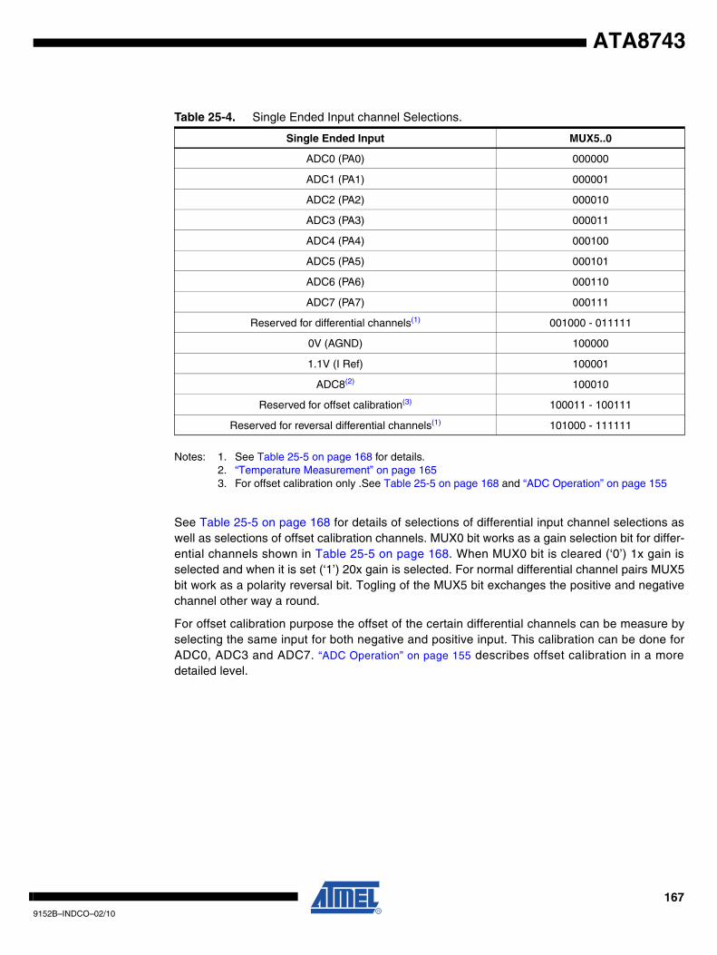
ATA8743
Notes: 1. See Table 25-5 on page 168 for details.2. “Temperature Measurement” on page 1653. For offset calibration only .See Table 25-5 on page 168 and “ADC Operation” on page 155
See Table 25-5 on page 168 for details of selections of differential input channel selections aswell as selections of offset calibration channels. MUX0 bit works as a gain selection bit for differ-ential channels shown in Table 25-5 on page 168. When MUX0 bit is cleared (‘0’) 1x gain isselected and when it is set (‘1’) 20x gain is selected. For normal differential channel pairs MUX5bit work as a polarity reversal bit. Togling of the MUX5 bit exchanges the positive and negativechannel other way a round.
For offset calibration purpose the offset of the certain differential channels can be measure byselecting the same input for both negative and positive input. This calibration can be done forADC0, ADC3 and ADC7. “ADC Operation” on page 155 describes offset calibration in a moredetailed level.
Table 25-4. Single Ended Input channel Selections.
Single Ended Input MUX5..0
ADC0 (PA0) 000000
ADC1 (PA1) 000001
ADC2 (PA2) 000010
ADC3 (PA3) 000011
ADC4 (PA4) 000100
ADC5 (PA5) 000101
ADC6 (PA6) 000110
ADC7 (PA7) 000111
Reserved for differential channels(1) 001000 - 011111
0V (AGND) 100000
1.1V (I Ref) 100001
ADC8(2) 100010
Reserved for offset calibration(3) 100011 - 100111
Reserved for reversal differential channels(1) 101000 - 111111
1679152B–INDCO–02/10
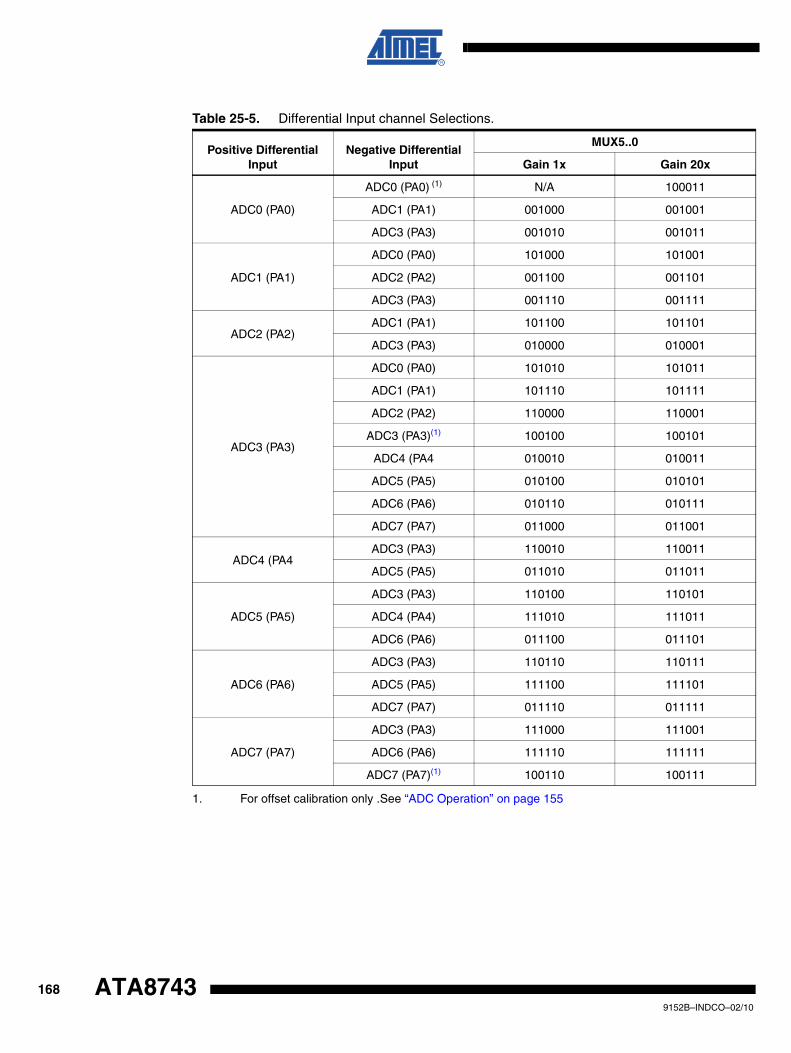
Table 25-5. Differential Input channel Selections.
Positive Differential Input
Negative Differential Input
MUX5..0
Gain 1x Gain 20x
ADC0 (PA0)
ADC0 (PA0) (1)
1. For offset calibration only .See “ADC Operation” on page 155
N/A 100011
ADC1 (PA1) 001000 001001
ADC3 (PA3) 001010 001011
ADC1 (PA1)
ADC0 (PA0) 101000 101001
ADC2 (PA2) 001100 001101
ADC3 (PA3) 001110 001111
ADC2 (PA2)ADC1 (PA1) 101100 101101
ADC3 (PA3) 010000 010001
ADC3 (PA3)
ADC0 (PA0) 101010 101011
ADC1 (PA1) 101110 101111
ADC2 (PA2) 110000 110001
ADC3 (PA3)(1) 100100 100101
ADC4 (PA4 010010 010011
ADC5 (PA5) 010100 010101
ADC6 (PA6) 010110 010111
ADC7 (PA7) 011000 011001
ADC4 (PA4ADC3 (PA3) 110010 110011
ADC5 (PA5) 011010 011011
ADC5 (PA5)
ADC3 (PA3) 110100 110101
ADC4 (PA4) 111010 111011
ADC6 (PA6) 011100 011101
ADC6 (PA6)
ADC3 (PA3) 110110 110111
ADC5 (PA5) 111100 111101
ADC7 (PA7) 011110 011111
ADC7 (PA7)
ADC3 (PA3) 111000 111001
ADC6 (PA6) 111110 111111
ADC7 (PA7)(1) 100110 100111
1689152B–INDCO–02/10
ATA8743
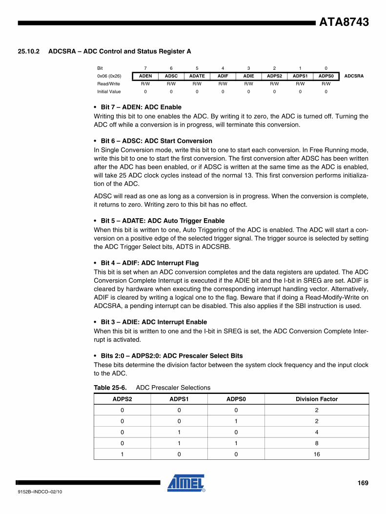
ATA8743
25.10.2 ADCSRA – ADC Control and Status Register A
• Bit 7 – ADEN: ADC EnableWriting this bit to one enables the ADC. By writing it to zero, the ADC is turned off. Turning theADC off while a conversion is in progress, will terminate this conversion.
• Bit 6 – ADSC: ADC Start ConversionIn Single Conversion mode, write this bit to one to start each conversion. In Free Running mode,write this bit to one to start the first conversion. The first conversion after ADSC has been writtenafter the ADC has been enabled, or if ADSC is written at the same time as the ADC is enabled,will take 25 ADC clock cycles instead of the normal 13. This first conversion performs initializa-tion of the ADC.
ADSC will read as one as long as a conversion is in progress. When the conversion is complete,it returns to zero. Writing zero to this bit has no effect.
• Bit 5 – ADATE: ADC Auto Trigger EnableWhen this bit is written to one, Auto Triggering of the ADC is enabled. The ADC will start a con-version on a positive edge of the selected trigger signal. The trigger source is selected by settingthe ADC Trigger Select bits, ADTS in ADCSRB.
• Bit 4 – ADIF: ADC Interrupt FlagThis bit is set when an ADC conversion completes and the data registers are updated. The ADCConversion Complete Interrupt is executed if the ADIE bit and the I-bit in SREG are set. ADIF iscleared by hardware when executing the corresponding interrupt handling vector. Alternatively,ADIF is cleared by writing a logical one to the flag. Beware that if doing a Read-Modify-Write onADCSRA, a pending interrupt can be disabled. This also applies if the SBI instruction is used.
• Bit 3 – ADIE: ADC Interrupt EnableWhen this bit is written to one and the I-bit in SREG is set, the ADC Conversion Complete Inter-rupt is activated.
• Bits 2:0 – ADPS2:0: ADC Prescaler Select BitsThese bits determine the division factor between the system clock frequency and the input clockto the ADC.
Bit 7 6 5 4 3 2 1 0
0x06 (0x26) ADEN ADSC ADATE ADIF ADIE ADPS2 ADPS1 ADPS0 ADCSRA
Read/Write R/W R/W R/W R/W R/W R/W R/W R/W
Initial Value 0 0 0 0 0 0 0 0
Table 25-6. ADC Prescaler Selections
ADPS2 ADPS1 ADPS0 Division Factor
0 0 0 2
0 0 1 2
0 1 0 4
0 1 1 8
1 0 0 16
1699152B–INDCO–02/10
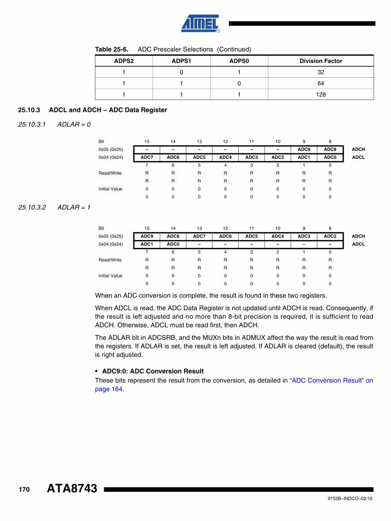
25.10.3 ADCL and ADCH – ADC Data Register
25.10.3.1 ADLAR = 0
25.10.3.2 ADLAR = 1
When an ADC conversion is complete, the result is found in these two registers.
When ADCL is read, the ADC Data Register is not updated until ADCH is read. Consequently, ifthe result is left adjusted and no more than 8-bit precision is required, it is sufficient to readADCH. Otherwise, ADCL must be read first, then ADCH.
The ADLAR bit in ADCSRB, and the MUXn bits in ADMUX affect the way the result is read fromthe registers. If ADLAR is set, the result is left adjusted. If ADLAR is cleared (default), the resultis right adjusted.
• ADC9:0: ADC Conversion ResultThese bits represent the result from the conversion, as detailed in “ADC Conversion Result” onpage 164.
1 0 1 32
1 1 0 64
1 1 1 128
Table 25-6. ADC Prescaler Selections (Continued)
ADPS2 ADPS1 ADPS0 Division Factor
Bit 15 14 13 12 11 10 9 8
0x05 (0x25) – – – – – – ADC9 ADC8 ADCH
0x04 (0x24) ADC7 ADC6 ADC5 ADC4 ADC3 ADC2 ADC1 ADC0 ADCL
7 6 5 4 3 2 1 0
Read/Write R R R R R R R R
R R R R R R R R
Initial Value 0 0 0 0 0 0 0 0
0 0 0 0 0 0 0 0
Bit 15 14 13 12 11 10 9 8
0x05 (0x25) ADC9 ADC8 ADC7 ADC6 ADC5 ADC4 ADC3 ADC2 ADCH
0x04 (0x24) ADC1 ADC0 – – – – – – ADCL
7 6 5 4 3 2 1 0
Read/Write R R R R R R R R
R R R R R R R R
Initial Value 0 0 0 0 0 0 0 0
0 0 0 0 0 0 0 0
1709152B–INDCO–02/10
ATA8743
ATA8743
25.10.4 ADCSRB – ADC Control and Status Register B
• Bits 7 – BIN: Bipolar Input ModeThe gain stage is working in the unipolar mode as default, but the bipolar mode can be selectedby writing the BIN bit in the ADCSRB register. In the unipolar mode only one-sided conversionsare supported and the voltage on the positive input must always be larger than the voltage onthe negative input. Otherwise the result is saturated to the voltage reference. In the bipolar modetwo-sided conversions are supported and the result is represented in the two’s complementform. In the unipolar mode the resolution is 10 bits and the bipolar mode the resolution is 9 bits +1 sign bit.
• Bit 6 – ACME: Analog Comparator Multiplexer EnableSee “ADCSRB – ADC Control and Status Register B” on page 152.
• Bit 5 – Res: Reserved BitThis bit is reserved bit in the ATtiny24/44/84 and will always read as what was wrote there.
• Bit 4 – ADLAR: ADC Left Adjust ResultThe ADLAR bit affects the presentation of the ADC conversion result in the ADC Data Register.Write one to ADLAR to left adjust the result. Otherwise, the result is right adjusted. Changing theADLAR bit will affect the ADC Data Register immediately, regardless of any ongoing conver-sions. For a complete description of this bit, see “ADCL and ADCH – ADC Data Register” onpage 170.
• Bit 3 – Res: Reserved BitThis bit is reserved bit in the ATtiny24/44/84 and will always read as what was wrote there.
• Bits 2:0 – ADTS2:0: ADC Auto Trigger SourceIf ADATE in ADCSRA is written to one, the value of these bits selects which source will triggeran ADC conversion. If ADATE is cleared, the ADTS2:0 settings will have no effect. A conversionwill be triggered by the rising edge of the selected Interrupt Flag. Note that switching from a trig-ger source that is cleared to a trigger source that is set, will generate a positive edge on thetrigger signal. If ADEN in ADCSRA is set, this will start a conversion. Switching to Free Runningmode (ADTS[2:0]=0) will not cause a trigger event, even if the ADC Interrupt Flag is set.
Bit 7 6 5 4 3 2 1 0
0x03 (0x23) BIN ACME – ADLAR – ADTS2 ADTS1 ADTS0 ADCSRB
Read/Write R/W R/W R/W R/W R/W R/W R/W R/W
Initial Value 0 0 0 0 0 0 0 0
Table 25-7. ADC Auto Trigger Source Selections
ADTS2 ADTS1 ADTS0 Trigger Source
0 0 0 Free Running mode
0 0 1 Analog Comparator
0 1 0 External Interrupt Request 0
0 1 1 Timer/Counter0 Compare Match A
1 0 0 Timer/Counter0 Overflow
1719152B–INDCO–02/10
25.10.5 DIDR0 – Digital Input Disable Register 0
• Bits 7..0 – ADC7D..ADC0D: ADC7..0 Digital Input DisableWhen this bit is written logic one, the digital input buffer on the corresponding ADC pin is dis-abled. The corresponding PIN register bit will always read as zero when this bit is set. When ananalog signal is applied to the ADC7..0 pin and the digital input from this pin is not needed, thisbit should be written logic one to reduce power consumption in the digital input buffer.
1 0 1 Timer/Counter1 Compare Match B
1 1 0 Timer/Counter1 Overflow
1 1 1 Timer/Counter1 Capture Event
Table 25-7. ADC Auto Trigger Source Selections
ADTS2 ADTS1 ADTS0 Trigger Source
Bit 7 6 5 4 3 2 1 0
0x01 (0x21) ADC7D ADC6D ADC5D ADC4D ADC3D ADC2D ADC1D ADC0D DIDR0
Read/Write R/W R/W R/W R/W R/W R/W R/W R/W
Initial Value 0 0 0 0 0 0 0 0
1729152B–INDCO–02/10
ATA8743
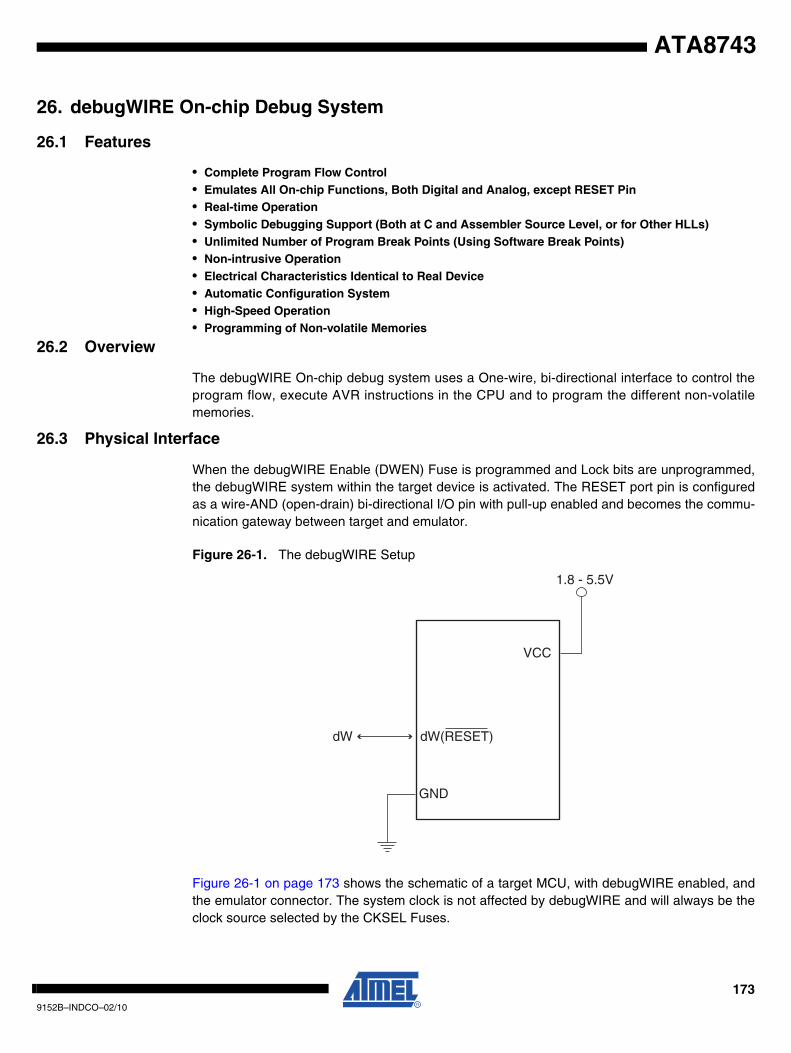
ATA8743
26. debugWIRE On-chip Debug System
26.1 Features
• Complete Program Flow Control• Emulates All On-chip Functions, Both Digital and Analog, except RESET Pin• Real-time Operation• Symbolic Debugging Support (Both at C and Assembler Source Level, or for Other HLLs)• Unlimited Number of Program Break Points (Using Software Break Points)• Non-intrusive Operation• Electrical Characteristics Identical to Real Device• Automatic Configuration System• High-Speed Operation• Programming of Non-volatile Memories
26.2 Overview
The debugWIRE On-chip debug system uses a One-wire, bi-directional interface to control theprogram flow, execute AVR instructions in the CPU and to program the different non-volatilememories.
26.3 Physical Interface
When the debugWIRE Enable (DWEN) Fuse is programmed and Lock bits are unprogrammed,the debugWIRE system within the target device is activated. The RESET port pin is configuredas a wire-AND (open-drain) bi-directional I/O pin with pull-up enabled and becomes the commu-nication gateway between target and emulator.
Figure 26-1. The debugWIRE Setup
Figure 26-1 on page 173 shows the schematic of a target MCU, with debugWIRE enabled, andthe emulator connector. The system clock is not affected by debugWIRE and will always be theclock source selected by the CKSEL Fuses.
dW
GND
dW(RESET)
VCC
1.8 - 5.5V
1739152B–INDCO–02/10
When designing a system where debugWIRE will be used, the following observations must bemade for correct operation:
• Pull-Up resistor on the dW/(RESET) line must be in the range of 10k to 20 kΩ. However, the pull-up resistor is optional.
• Connecting the RESET pin directly to VCC will not work.
• Capacitors inserted on the RESET pin must be disconnected when using debugWire.
• All external reset sources must be disconnected.
26.4 Software Break Points
debugWIRE supports Program memory Break Points by the AVR Break instruction. Setting aBreak Point in AVR Studio® will insert a BREAK instruction in the Program memory. The instruc-tion replaced by the BREAK instruction will be stored. When program execution is continued, thestored instruction will be executed before continuing from the Program memory. A break can beinserted manually by putting the BREAK instruction in the program.
The Flash must be re-programmed each time a Break Point is changed. This is automaticallyhandled by AVR Studio through the debugWIRE interface. The use of Break Points will thereforereduce the Flash Data retention. Devices used for debugging purposes should not be shipped toend customers.
26.5 Limitations of debugWIRE
The debugWIRE communication pin (dW) is physically located on the same pin as ExternalReset (RESET). An External Reset source is therefore not supported when the debugWIRE isenabled.
The debugWIRE system accurately emulates all I/O functions when running at full speed, i.e.,when the program in the CPU is running. When the CPU is stopped, care must be taken whileaccessing some of the I/O Registers via the debugger (AVR Studio). See the debugWIRE docu-mentation for detailed description of the limitations.
A programmed DWEN Fuse enables some parts of the clock system to be running in all sleepmodes. This will increase the power consumption while in sleep. Thus, the DWEN Fuse shouldbe disabled when debugWire is not used.
26.6 Register Description
The following section describes the registers used with the debugWire.
26.6.1 DWDR – debugWire Data Register
The DWDR Register provides a communication channel from the running program in the MCUto the debugger. This register is only accessible by the debugWIRE and can therefore not beused as a general purpose register in the normal operations.
Bit 7 6 5 4 3 2 1 0
0x27 (0x47) DWDR[7:0] DWDR
Read/Write R/W R/W R/W R/W R/W R/W R/W R/W
Initial Value 0 0 0 0 0 0 0 0
1749152B–INDCO–02/10
ATA8743
ATA8743
27. Self-Programming the Flash
The device provides a Self-Programming mechanism for downloading and uploading programcode by the MCU itself. The Self-Programming can use any available data interface and associ-ated protocol to read code and write (program) that code into the Program memory.
The Program memory is updated in a page by page fashion. Before programming a page withthe data stored in the temporary page buffer, the page must be erased. The temporary page buf-fer is filled one word at a time using SPM and the buffer can be filled either before the PageErase command or between a Page Erase and a Page Write operation:
Alternative 1, fill the buffer before a Page Erase
• Fill temporary page buffer
• Perform a Page Erase
• Perform a Page Write
Alternative 2, fill the buffer after Page Erase
• Perform a Page Erase
• Fill temporary page buffer
• Perform a Page Write
If only a part of the page needs to be changed, the rest of the page must be stored (for examplein the temporary page buffer) before the erase, and then be re-written. When using alternative 1,the Boot Loader provides an effective Read-Modify-Write feature which allows the user softwareto first read the page, do the necessary changes, and then write back the modified data. If alter-native 2 is used, it is not possible to read the old data while loading since the page is alreadyerased. The temporary page buffer can be accessed in a random sequence. It is essential thatthe page address used in both the Page Erase and Page Write operation is addressing the samepage.
27.0.1 Performing Page Erase by SPM
To execute Page Erase, set up the address in the Z-pointer, write “00000011” to SPMCSR andexecute SPM within four clock cycles after writing SPMCSR. The data in R1 and R0 is ignored.The page address must be written to PCPAGE in the Z-register. Other bits in the Z-pointer willbe ignored during this operation.
• The CPU is halted during the Page Erase operation.
27.0.2 Filling the Temporary Buffer (Page Loading)
To write an instruction word, set up the address in the Z-pointer and data in R1:R0, write“00000001” to SPMCSR and execute SPM within four clock cycles after writing SPMCSR. Thecontent of PCWORD in the Z-register is used to address the data in the temporary buffer. Thetemporary buffer will auto-erase after a Page Write operation or by writing the CTPB bit inSPMCSR. It is also erased after a system reset. Note that it is not possible to write more thanone time to each address without erasing the temporary buffer.
If the EEPROM is written in the middle of an SPM Page Load operation, all data loaded will belost.
1759152B–INDCO–02/10
27.0.3 Performing a Page Write
To execute Page Write, set up the address in the Z-pointer, write “00000101” to SPMCSR andexecute SPM within four clock cycles after writing SPMCSR. The data in R1 and R0 is ignored.The page address must be written to PCPAGE. Other bits in the Z-pointer must be written tozero during this operation.
• The CPU is halted during the Page Write operation.
27.1 Addressing the Flash During Self-Programming
The Z-pointer is used to address the SPM commands.
Since the Flash is organized in pages (see Table 28-7 on page 183), the Program Counter canbe treated as having two different sections. One section, consisting of the least significant bits, isaddressing the words within a page, while the most significant bits are addressing the pages.This is shown in Figure 28-1 on page 184. Note that the Page Erase and Page Write operationsare addressed independently. Therefore it is of major importance that the software addressesthe same page in both the Page Erase and Page Write operation.
The LPM instruction uses the Z-pointer to store the address. Since this instruction addresses theFlash byte-by-byte, also the LSB (bit Z0) of the Z-pointer is used.
Figure 27-1. Addressing the Flash During SPM(1)
Note: 1. The different variables used in Figure 27-1 are listed in Table 28-7 on page 183.
Bit 15 14 13 12 11 10 9 8
ZH (R31) Z15 Z14 Z13 Z12 Z11 Z10 Z9 Z8
ZL (R30) Z7 Z6 Z5 Z4 Z3 Z2 Z1 Z0
7 6 5 4 3 2 1 0
PROGRAM MEMORY
0115
Z - REGISTER
BIT
0
ZPAGEMSB
WORD ADDRESSWITHIN A PAGE
PAGE ADDRESSWITHIN THE FLASH
ZPCMSB
INSTRUCTION WORD
PAGE PCWORD[PAGEMSB:0]:
00
01
02
PAGEEND
PAGE
PCWORDPCPAGE
PCMSB PAGEMSBPROGRAMCOUNTER
1769152B–INDCO–02/10
ATA8743
ATA8743
27.1.1 EEPROM Write Prevents Writing to SPMCSR
Note that an EEPROM write operation will block all software programming to Flash. Reading theFuses and Lock bits from software will also be prevented during the EEPROM write operation. Itis recommended that the user checks the status bit (EEPE) in the EECR Register and verifiesthat the bit is cleared before writing to the SPMCSR Register.
27.1.2 Reading the Fuse and Lock Bits from Software
It is possible to read both the Fuse and Lock bits from software. To read the Lock bits, load theZ-pointer with 0x0001 and set the RFLB and SPMEN bits in SPMCSR. When an LPM instructionis executed within three CPU cycles after the RFLB and SPMEN bits are set in SPMCSR, thevalue of the Lock bits will be loaded in the destination register. The RFLB and SPMEN bits willauto-clear upon completion of reading the Lock bits or if no LPM instruction is executed withinthree CPU cycles or no SPM instruction is executed within four CPU cycles. When RFLB andSPMEN are cleared, LPM will work as described in the Instruction set Manual.
The algorithm for reading the Fuse Low byte is similar to the one described above for readingthe Lock bits. To read the Fuse Low byte, load the Z-pointer with 0x0000 and set the RFLB andSPMEN bits in SPMCSR. When an LPM instruction is executed within three cycles after theRFLB and SPMEN bits are set in the SPMCSR, the value of the Fuse Low byte (FLB) will beloaded in the destination register as shown below. See Table 28-5 on page 182 for a detaileddescription and mapping of the Fuse Low byte.
Similarly, when reading the Fuse High byte, load 0x0003 in the Z-pointer. When an LPM instruc-tion is executed within three cycles after the RFLB and SPMEN bits are set in the SPMCSR, thevalue of the Fuse High byte (FHB) will be loaded in the destination register as shown below. SeeTable 28-4 on page 181 for detailed description and mapping of the Fuse High byte.
Fuse and Lock bits that are programmed, will be read as zero. Fuse and Lock bits that areunprogrammed, will be read as one.
27.1.3 Preventing Flash Corruption
During periods of low VCC, the Flash program can be corrupted because the supply voltage istoo low for the CPU and the Flash to operate properly. These issues are the same as for boardlevel systems using the Flash, and the same design solutions should be applied.
A Flash program corruption can be caused by two situations when the voltage is too low. First, aregular write sequence to the Flash requires a minimum voltage to operate correctly. Secondly,the CPU itself can execute instructions incorrectly, if the supply voltage for executing instructionsis too low.
Bit 7 6 5 4 3 2 1 0
Rd – – – – – – LB2 LB1
Bit 7 6 5 4 3 2 1 0
Rd FLB7 FLB6 FLB5 FLB4 FLB3 FLB2 FLB1 FLB0
Bit 7 6 5 4 3 2 1 0
Rd FHB7 FHB6 FHB5 FHB4 FHB3 FHB2 FHB1 FHB0
1779152B–INDCO–02/10
Flash corruption can easily be avoided by following these design recommendations (one issufficient):
1. Keep the AVR RESET active (low) during periods of insufficient power supply voltage. This can be done by enabling the internal Brown-out Detector (BOD) if the operating volt-age matches the detection level. If not, an external low VCC reset protection circuit can be used. If a reset occurs while a write operation is in progress, the write operation will be completed provided that the power supply voltage is sufficient.
2. Keep the AVR core in Power-down sleep mode during periods of low VCC. This will pre-vent the CPU from attempting to decode and execute instructions, effectively protecting the SPMCSR Register and thus the Flash from unintentional writes.
27.1.4 Programming Time for Flash when Using SPM
The calibrated RC Oscillator is used to time Flash accesses. Table 27-1 shows the typical pro-gramming time for Flash accesses from the CPU.
Note: 1. The min and max programming times is per individual operation.
27.2 Register Description
27.2.1 SPMCSR – Store Program Memory Control and Status Register
The Store Program Memory Control and Status Register contains the control bits needed to con-trol the Program memory operations.
• Bits 7..5 – Res: Reserved BitsThese bits are reserved bits in the ATtiny24/44/84 and always read as zero.
• Bit 4 – CTPB: Clear Temporary Page BufferIf the CTPB bit is written while filling the temporary page buffer, the temporary page buffer will becleared and the data will be lost.
• Bit 3 – RFLB: Read Fuse and Lock BitsAn LPM instruction within three cycles after RFLB and SPMEN are set in the SPMCSR Register,will read either the Lock bits or the Fuse bits (depending on Z0 in the Z-pointer) into the destina-tion register. See “EEPROM Write Prevents Writing to SPMCSR” on page 177 for details.
• Bit 2 – PGWRT: Page WriteIf this bit is written to one at the same time as SPMEN, the next SPM instruction within four clockcycles executes Page Write, with the data stored in the temporary buffer. The page address istaken from the high part of the Z-pointer. The data in R1 and R0 are ignored. The PGWRT bit
Table 27-1. SPM Programming Time(1)
Symbol Min Programming Time Max Programming Time
Flash write (Page Erase, Page Write, and write Lock bits by SPM)
3.7 ms 4.5 ms
Bit 7 6 5 4 3 2 1 0
0x37 (0x57) – – – CTPB RFLB PGWRT PGERS SPMEN SPMCSR
Read/Write R R R R/W R/W R/W R/W R/W
Initial Value 0 0 0 0 0 0 0 0
1789152B–INDCO–02/10
ATA8743
ATA8743
will auto-clear upon completion of a Page Write, or if no SPM instruction is executed within fourclock cycles. The CPU is halted during the entire Page Write operation.
• Bit 1 – PGERS: Page EraseIf this bit is written to one at the same time as SPMEN, the next SPM instruction within four clockcycles executes Page Erase. The page address is taken from the high part of the Z-pointer. Thedata in R1 and R0 are ignored. The PGERS bit will auto-clear upon completion of a Page Erase,or if no SPM instruction is executed within four clock cycles. The CPU is halted during the entirePage Write operation.
• Bit 0 – SPMEN: Store Program Memory EnableThis bit enables the SPM instruction for the next four clock cycles. If written to one together witheither CTPB, RFLB, PGWRT, or PGERS, the following SPM instruction will have a specialmeaning, see description above. If only SPMEN is written, the following SPM instruction willstore the value in R1:R0 in the temporary page buffer addressed by the Z-pointer. The LSB ofthe Z-pointer is ignored. The SPMEN bit will auto-clear upon completion of an SPM instruction,or if no SPM instruction is executed within four clock cycles. During Page Erase and Page Write,the SPMEN bit remains high until the operation is completed.
Writing any other combination than “10001”, “01001”, “00101”, “00011” or “00001” in the lowerfive bits will have no effect.
1799152B–INDCO–02/10
28. Memory Programming
This section describes the different methods for Programming the ATtiny24/44/84 memories.
28.1 Program And Data Memory Lock Bits
The ATtiny24/44/84 provides two Lock bits which can be left unprogrammed (“1”) or can be pro-grammed (“0”) to obtain the additional security listed in Table 28-2 on page 180. The Lock bitscan only be erased to “1” with the Chip Erase command.
Program memory can be read out via the debugWIRE interface when the DWEN fuse is pro-grammed, even if the Lock Bits are set. Thus, when Lock Bit security is required, should alwaysdebugWIRE be disabled by clearing the DWEN fuse.
Note: 1. “1” means unprogrammed, “0” means programmed
Notes: 1. Program the Fuse bits before programming the LB1 and LB2.2. “1” means unprogrammed, “0” means programmed
Table 28-1. Lock Bit Byte(1)
Lock Bit Byte Bit No Description Default Value
7 – 1 (unprogrammed)
6 – 1 (unprogrammed)
5 – 1 (unprogrammed)
4 – 1 (unprogrammed)
3 – 1 (unprogrammed)
2 – 1 (unprogrammed)
LB2 1 Lock bit 1 (unprogrammed)
LB1 0 Lock bit 1 (unprogrammed)
Table 28-2. Lock Bit Protection Modes(1)(2)
Memory Lock Bits Protection Type
LB Mode LB2 LB1
1 1 1 No memory lock features enabled.
2 1 0
Further programming of the Flash and EEPROM is disabled in High-voltage and Serial Programming mode. The Fuse bits are locked in both Serial and High-voltage Programming mode.(1) debugWire is disabled.
3 0 0
Further programming and verification of the Flash and EEPROM is disabled in High-voltage and Serial Programming mode. The Fuse bits are locked in both Serial and High-voltage Programming mode.(1) debugWire is disabled.
1809152B–INDCO–02/10
ATA8743
ATA8743
28.2 Fuse Bytes
The ATtiny24/44/84 has three Fuse bytes. Table 28-4 on page 181 to Table 28-5 on page 182describe briefly the functionality of all the fuses and how they are mapped into the Fuse bytes.Note that the fuses are read as logical zero, “0”, if they are programmed.
Notes: 1. See “Alternate Functions of Port B” on page 84 for description of RSTDISBL and DWEN Fuses. When programming the RSTDISBL Fuse, High-voltage Serial programming has to be used to change fuses to perform further programming
2. DWEN must be unprogrammed when Lock Bit security is required. See “Program And Data Memory Lock Bits” on page 180.
3. The SPIEN Fuse is not accessible in SPI Programming mode.4. See “WDT Configuration as a Function of the Fuse Settings of WDTON” on page 60 for
details.5. See Table 29-5 on page 198 for BODLEVEL Fuse decoding.
Table 28-3. Fuse Extended Byte
Fuse High Byte Bit No Description Default Value
7 - 1 (unprogrammed)
6 - 1 (unprogrammed)
5 - 1 (unprogrammed)
4 - 1 (unprogrammed)
3 - 1 (unprogrammed)
2 - 1 (unprogrammed)
1 - 1 (unprogrammed)
SELFPRGEN 0 Self-Programming Enable 1 (unprogrammed)
Table 28-4. Fuse High Byte
Fuse High Byte Bit No Description Default Value
RSTDISBL(1) 7 External Reset disable 1 (unprogrammed)
DWEN(2) 6 DebugWIRE Enable 1 (unprogrammed)
SPIEN(3) 6Enable Serial Program and Data Downloading
0 (programmed, SPI prog. enabled)
WDTON(4) 4 Watchdog Timer always on 1 (unprogrammed)
EESAVE 3EEPROM memory is preserved through the Chip Erase
1 (unprogrammed, EEPROM not preserved)
BODLEVEL2(5) 2 Brown-out Detector trigger level 1 (unprogrammed)
BODLEVEL1(5) 1 Brown-out Detector trigger level 1 (unprogrammed)
BODLEVEL0(5) 0 Brown-out Detector trigger level 1 (unprogrammed)
1819152B–INDCO–02/10
Notes: 1. See “System Clock Prescaler” on page 47 for details.2. The default value of SUT1..0 results in maximum start-up time for the default clock source.
See Table 14-7 on page 45 for details.3. The default setting of CKSEL3..0 results in internal RC Oscillator @ 8.0 MHz. See Table 14-6
on page 45 for details.
The status of the Fuse bits is not affected by Chip Erase. Note that the Fuse bits are locked ifLock bit1 (LB1) is programmed. Program the Fuse bits before programming the Lock bits.
28.2.1 Latching of Fuses
The fuse values are latched when the device enters programming mode and changes of thefuse values will have no effect until the part leaves Programming mode. This does not apply tothe EESAVE Fuse which will take effect once it is programmed. The fuses are also latched onPower-up in Normal mode.
28.3 Signature Bytes
All Atmel microcontrollers have a three-byte signature code which identifies the device. Thiscode can be read in both serial and High-voltage Programming mode, also when the device islocked. The three bytes reside in a separate address space. For the ATtiny24/44/84 the signa-ture bytes are given in Table 28-6.
28.4 Calibration Byte
Signature area of the ATtiny24/44/84 has one byte of calibration data for the internal RC Oscilla-tor. This byte resides in the high byte of address 0x000. During reset, this byte is automaticallywritten into the OSCCAL Register to ensure correct frequency of the calibrated RC Oscillator.
Table 28-5. Fuse Low Byte
Fuse Low Byte Bit No Description Default Value
CKDIV8(1) 7 Divide clock by 8 0 (programmed)
CKOUT 6 Clock Output Enable 1 (unprogrammed)
SUT1 5 Select start-up time 1 (unprogrammed)(2)
SUT0 4 Select start-up time 0 (programmed)(2)
CKSEL3 3 Select Clock source 0 (programmed)(3)
CKSEL2 2 Select Clock source 0 (programmed)(3)
CKSEL1 1 Select Clock source 1 (unprogrammed)(3)
CKSEL0 0 Select Clock source 0 (programmed)(3)
Table 28-6. Device ID
Parts
Signature Bytes Address
0x000 0x001 0x002
ATtiny24 0x1E 0x91 0x0B
ATtiny44 0x1E 0x92 0x07
ATtiny84 0x1E 0x93 0x0C
1829152B–INDCO–02/10
ATA8743
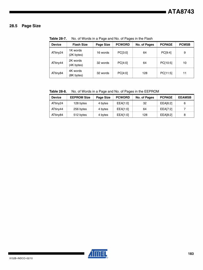
ATA8743
28.5 Page Size
Table 28-7. No. of Words in a Page and No. of Pages in the Flash
Device Flash Size Page Size PCWORD No. of Pages PCPAGE PCMSB
ATtiny241K words
(2K bytes)16 words PC[3:0] 64 PC[9:4] 9
ATtiny442K words
(4K bytes)32 words PC[4:0] 64 PC[10:5] 10
ATtiny844K words
(8K bytes)32 words PC[4:0] 128 PC[11:5] 11
Table 28-8. No. of Words in a Page and No. of Pages in the EEPROM
Device EEPROM Size Page Size PCWORD No. of Pages PCPAGE EEAMSB
ATtiny24 128 bytes 4 bytes EEA[1:0] 32 EEA[6:2] 6
ATtiny44 256 bytes 4 bytes EEA[1:0] 64 EEA[7:2] 7
ATtiny84 512 bytes 4 bytes EEA[1:0] 128 EEA[8:2] 8
1839152B–INDCO–02/10
28.6 Serial Downloading
Both the Flash and EEPROM memory arrays can be programmed using the serial SPI bus whileRESET is pulled to GND. The serial interface consists of pins SCK, MOSI (input) and MISO (out-put). After RESET is set low, the Programming Enable instruction needs to be executed firstbefore program/erase operations can be executed. NOTE, in Table 28-9 on page 184, the pinmapping for SPI programming is listed. Not all parts use the SPI pins dedicated for the internalSPI interface.
Figure 28-1. Serial Programming and Verify(1)
Note: 1. If the device is clocked by the internal Oscillator, it is no need to connect a clock source to the CLKI pin.
When programming the EEPROM, an auto-erase cycle is built into the self-timed programmingoperation (in the Serial mode ONLY) and there is no need to first execute the Chip Eraseinstruction. The Chip Erase operation turns the content of every memory location in both theProgram and EEPROM arrays into 0xFF.
Depending on CKSEL Fuses, a valid clock must be present. The minimum low and high periodsfor the serial clock (SCK) input are defined as follows:
Low: > 2 CPU clock cycles for fck < 12 MHz, 3 CPU clock cycles for fck >= 12 MHz
High: > 2 CPU clock cycles for fck < 12 MHz, 3 CPU clock cycles for fck >= 12 MHz
Table 28-9. Pin Mapping Serial Programming
Symbol Pins I/O Description
MOSI PA6 I Serial Data in
MISO PA5 O Serial Data out
SCK PA4 I Serial Clock
VCC
GND
SCK
MISO
MOSI
RESET
+1.8 - 5.5V
1849152B–INDCO–02/10
ATA8743
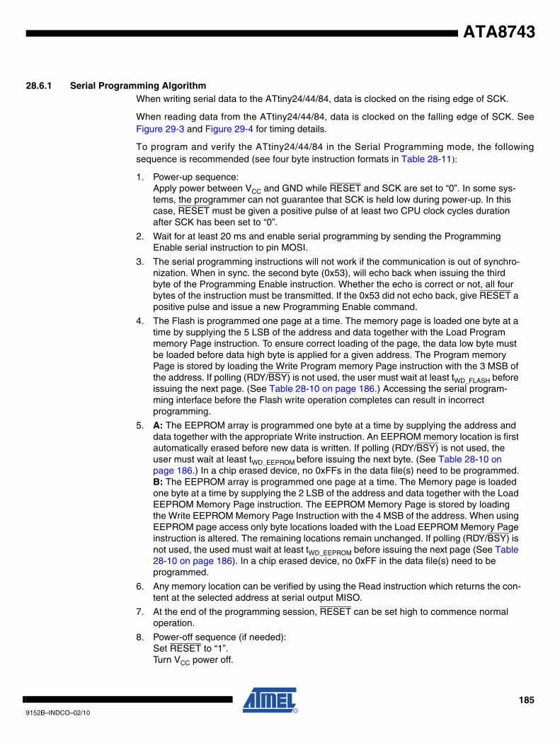
ATA8743
28.6.1 Serial Programming AlgorithmWhen writing serial data to the ATtiny24/44/84, data is clocked on the rising edge of SCK.
When reading data from the ATtiny24/44/84, data is clocked on the falling edge of SCK. SeeFigure 29-3 and Figure 29-4 for timing details.
To program and verify the ATtiny24/44/84 in the Serial Programming mode, the followingsequence is recommended (see four byte instruction formats in Table 28-11):
1. Power-up sequence:Apply power between VCC and GND while RESET and SCK are set to “0”. In some sys-tems, the programmer can not guarantee that SCK is held low during power-up. In this case, RESET must be given a positive pulse of at least two CPU clock cycles duration after SCK has been set to “0”.
2. Wait for at least 20 ms and enable serial programming by sending the Programming Enable serial instruction to pin MOSI.
3. The serial programming instructions will not work if the communication is out of synchro-nization. When in sync. the second byte (0x53), will echo back when issuing the third byte of the Programming Enable instruction. Whether the echo is correct or not, all four bytes of the instruction must be transmitted. If the 0x53 did not echo back, give RESET a positive pulse and issue a new Programming Enable command.
4. The Flash is programmed one page at a time. The memory page is loaded one byte at a time by supplying the 5 LSB of the address and data together with the Load Program memory Page instruction. To ensure correct loading of the page, the data low byte must be loaded before data high byte is applied for a given address. The Program memory Page is stored by loading the Write Program memory Page instruction with the 3 MSB of the address. If polling (RDY/BSY) is not used, the user must wait at least tWD_FLASH before issuing the next page. (See Table 28-10 on page 186.) Accessing the serial program-ming interface before the Flash write operation completes can result in incorrect programming.
5. A: The EEPROM array is programmed one byte at a time by supplying the address and data together with the appropriate Write instruction. An EEPROM memory location is first automatically erased before new data is written. If polling (RDY/BSY) is not used, the user must wait at least tWD_EEPROM before issuing the next byte. (See Table 28-10 on page 186.) In a chip erased device, no 0xFFs in the data file(s) need to be programmed.B: The EEPROM array is programmed one page at a time. The Memory page is loaded one byte at a time by supplying the 2 LSB of the address and data together with the Load EEPROM Memory Page instruction. The EEPROM Memory Page is stored by loading the Write EEPROM Memory Page Instruction with the 4 MSB of the address. When using EEPROM page access only byte locations loaded with the Load EEPROM Memory Page instruction is altered. The remaining locations remain unchanged. If polling (RDY/BSY) is not used, the used must wait at least tWD_EEPROM before issuing the next page (See Table 28-10 on page 186). In a chip erased device, no 0xFF in the data file(s) need to be programmed.
6. Any memory location can be verified by using the Read instruction which returns the con-tent at the selected address at serial output MISO.
7. At the end of the programming session, RESET can be set high to commence normal operation.
8. Power-off sequence (if needed):Set RESET to “1”.Turn VCC power off.
1859152B–INDCO–02/10
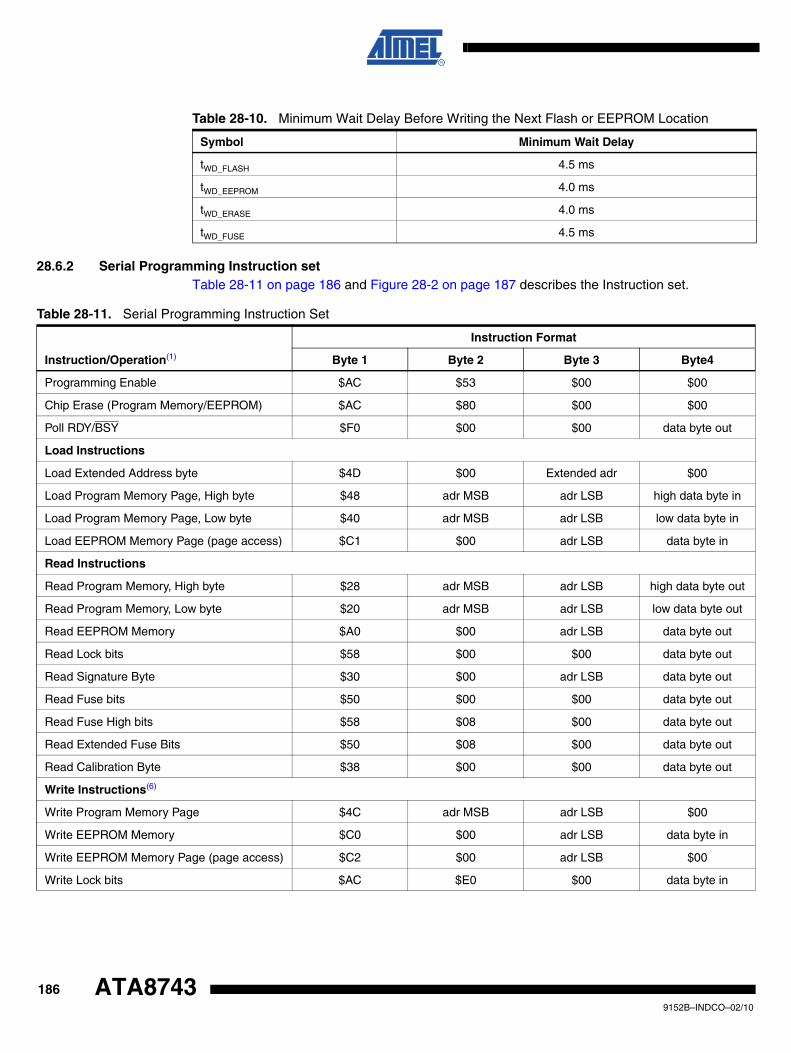
28.6.2 Serial Programming Instruction setTable 28-11 on page 186 and Figure 28-2 on page 187 describes the Instruction set.
Table 28-10. Minimum Wait Delay Before Writing the Next Flash or EEPROM Location
Symbol Minimum Wait Delay
tWD_FLASH 4.5 ms
tWD_EEPROM 4.0 ms
tWD_ERASE 4.0 ms
tWD_FUSE 4.5 ms
Table 28-11. Serial Programming Instruction Set
Instruction/Operation(1)
Instruction Format
Byte 1 Byte 2 Byte 3 Byte4
Programming Enable $AC $53 $00 $00
Chip Erase (Program Memory/EEPROM) $AC $80 $00 $00
Poll RDY/BSY $F0 $00 $00 data byte out
Load Instructions
Load Extended Address byte $4D $00 Extended adr $00
Load Program Memory Page, High byte $48 adr MSB adr LSB high data byte in
Load Program Memory Page, Low byte $40 adr MSB adr LSB low data byte in
Load EEPROM Memory Page (page access) $C1 $00 adr LSB data byte in
Read Instructions
Read Program Memory, High byte $28 adr MSB adr LSB high data byte out
Read Program Memory, Low byte $20 adr MSB adr LSB low data byte out
Read EEPROM Memory $A0 $00 adr LSB data byte out
Read Lock bits $58 $00 $00 data byte out
Read Signature Byte $30 $00 adr LSB data byte out
Read Fuse bits $50 $00 $00 data byte out
Read Fuse High bits $58 $08 $00 data byte out
Read Extended Fuse Bits $50 $08 $00 data byte out
Read Calibration Byte $38 $00 $00 data byte out
Write Instructions(6)
Write Program Memory Page $4C adr MSB adr LSB $00
Write EEPROM Memory $C0 $00 adr LSB data byte in
Write EEPROM Memory Page (page access) $C2 $00 adr LSB $00
Write Lock bits $AC $E0 $00 data byte in
1869152B–INDCO–02/10
ATA8743
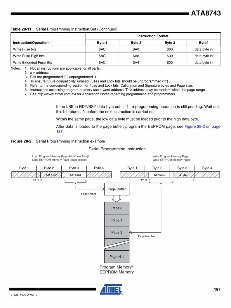
ATA8743
Notes: 1. Not all instructions are applicable for all parts.2. a = address3. Bits are programmed ‘0’, unprogrammed ‘1’.4. To ensure future compatibility, unused Fuses and Lock bits should be unprogrammed (‘1’) .5. Refer to the corresponding section for Fuse and Lock bits, Calibration and Signature bytes and Page size.6. Instructions accessing program memory use a word address. This address may be random within the page range.7. See http://www.atmel.com/avr for Application Notes regarding programming and programmers.
If the LSB in RDY/BSY data byte out is ‘1’, a programming operation is still pending. Wait untilthis bit returns ‘0’ before the next instruction is carried out.
Within the same page, the low data byte must be loaded prior to the high data byte.
After data is loaded to the page buffer, program the EEPROM page, see Figure 28-2 on page187.
Figure 28-2. Serial Programming Instruction example
Write Fuse bits $AC $A0 $00 data byte in
Write Fuse High bits $AC $A8 $00 data byte in
Write Extended Fuse Bits $AC $A4 $00 data byte in
Table 28-11. Serial Programming Instruction Set (Continued)
Instruction/Operation(1)
Instruction Format
Byte 1 Byte 2 Byte 3 Byte4
Byte 1 Byte 2 Byte 3 Byte 4
Adr LSB
Bit 15 B 0
Serial Programming Instruction
Program Memory/EEPROM Memory
Page 0
Page 1
Page 2
Page N-1
Page Buffer
Write Program Memory Page/Write EEPROM Memory Page
Load Program Memory Page (High/Low Byte)/Load EEPROM Memory Page (page access)
Byte 1 Byte 2 Byte 3 Byte 4
Bit 15 B 0
Adr MSB
Page Offset
Page Number
Adr MMSSBA AAdrr LLSBB
1879152B–INDCO–02/10
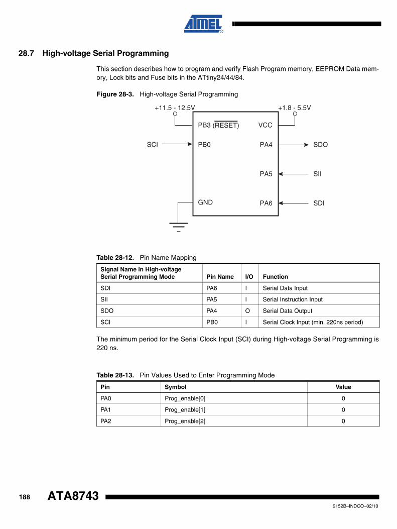
28.7 High-voltage Serial Programming
This section describes how to program and verify Flash Program memory, EEPROM Data mem-ory, Lock bits and Fuse bits in the ATtiny24/44/84.
Figure 28-3. High-voltage Serial Programming
The minimum period for the Serial Clock Input (SCI) during High-voltage Serial Programming is220 ns.
Table 28-12. Pin Name Mapping
Signal Name in High-voltage Serial Programming Mode Pin Name I/O Function
SDI PA6 I Serial Data Input
SII PA5 I Serial Instruction Input
SDO PA4 O Serial Data Output
SCI PB0 I Serial Clock Input (min. 220ns period)
Table 28-13. Pin Values Used to Enter Programming Mode
Pin Symbol Value
PA0 Prog_enable[0] 0
PA1 Prog_enable[1] 0
PA2 Prog_enable[2] 0
VCC
GND
SDO
SII
SDI
(RESET)
+1.8 - 5.5V
PA6
PA5
PA4
PB3
+11.5 - 12.5V
PB0SCI
1889152B–INDCO–02/10
ATA8743
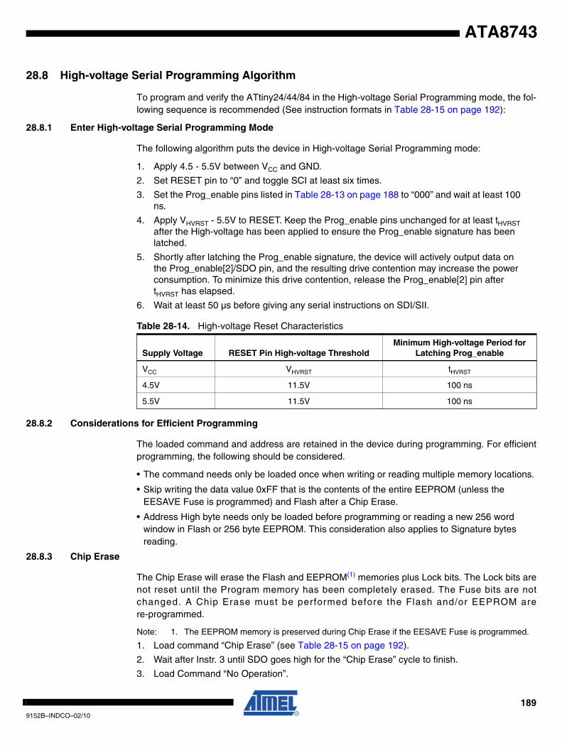
ATA8743
28.8 High-voltage Serial Programming Algorithm
To program and verify the ATtiny24/44/84 in the High-voltage Serial Programming mode, the fol-lowing sequence is recommended (See instruction formats in Table 28-15 on page 192):
28.8.1 Enter High-voltage Serial Programming Mode
The following algorithm puts the device in High-voltage Serial Programming mode:
1. Apply 4.5 - 5.5V between VCC and GND.
2. Set RESET pin to “0” and toggle SCI at least six times.
3. Set the Prog_enable pins listed in Table 28-13 on page 188 to “000” and wait at least 100 ns.
4. Apply VHVRST - 5.5V to RESET. Keep the Prog_enable pins unchanged for at least tHVRST after the High-voltage has been applied to ensure the Prog_enable signature has been latched.
5. Shortly after latching the Prog_enable signature, the device will actively output data on the Prog_enable[2]/SDO pin, and the resulting drive contention may increase the power consumption. To minimize this drive contention, release the Prog_enable[2] pin after tHVRST has elapsed.
6. Wait at least 50 µs before giving any serial instructions on SDI/SII.
28.8.2 Considerations for Efficient Programming
The loaded command and address are retained in the device during programming. For efficientprogramming, the following should be considered.
• The command needs only be loaded once when writing or reading multiple memory locations.
• Skip writing the data value 0xFF that is the contents of the entire EEPROM (unless the EESAVE Fuse is programmed) and Flash after a Chip Erase.
• Address High byte needs only be loaded before programming or reading a new 256 word window in Flash or 256 byte EEPROM. This consideration also applies to Signature bytes reading.
28.8.3 Chip Erase
The Chip Erase will erase the Flash and EEPROM(1) memories plus Lock bits. The Lock bits arenot reset until the Program memory has been completely erased. The Fuse bits are notchanged. A Chip Erase must be performed before the Flash and/or EEPROM arere-programmed.
Note: 1. The EEPROM memory is preserved during Chip Erase if the EESAVE Fuse is programmed.
1. Load command “Chip Erase” (see Table 28-15 on page 192).
2. Wait after Instr. 3 until SDO goes high for the “Chip Erase” cycle to finish.
3. Load Command “No Operation”.
Table 28-14. High-voltage Reset Characteristics
Supply Voltage RESET Pin High-voltage ThresholdMinimum High-voltage Period for
Latching Prog_enable
VCC VHVRST tHVRST
4.5V 11.5V 100 ns
5.5V 11.5V 100 ns
1899152B–INDCO–02/10
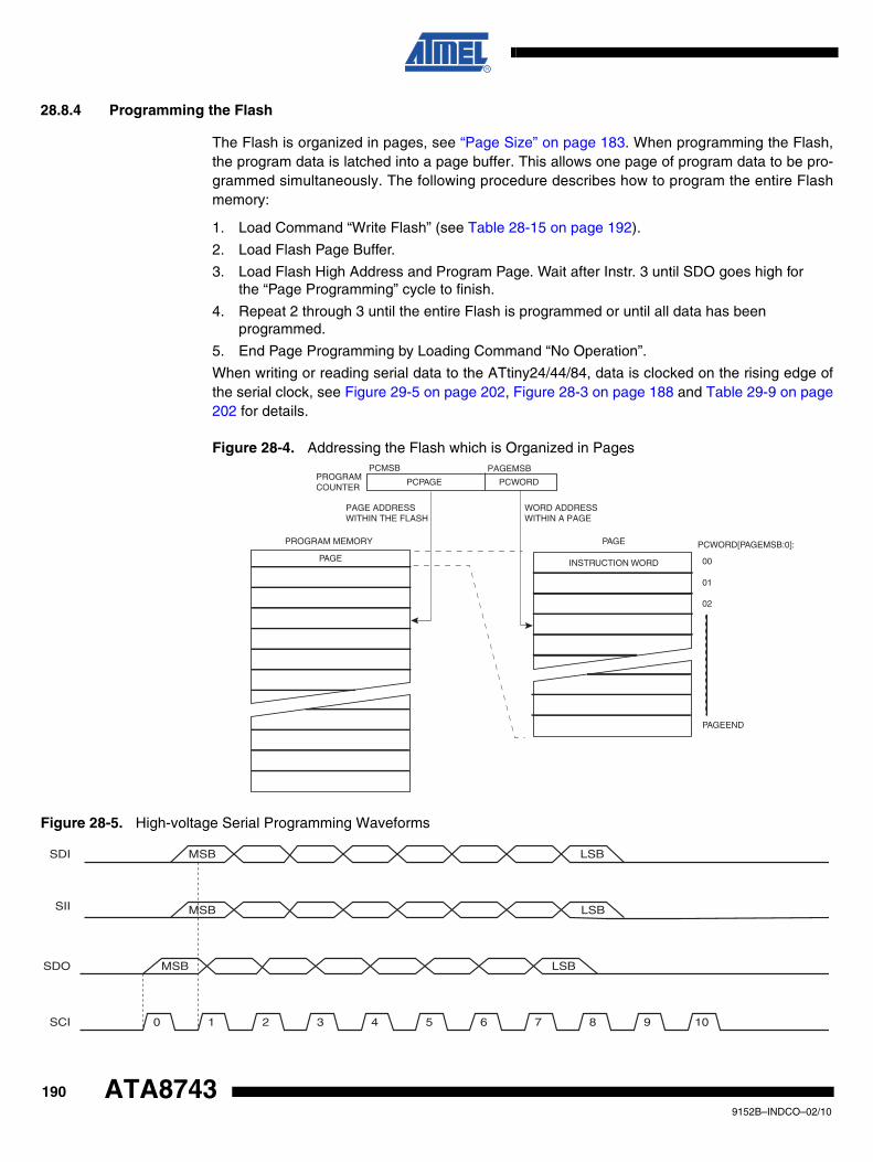
28.8.4 Programming the Flash
The Flash is organized in pages, see “Page Size” on page 183. When programming the Flash,the program data is latched into a page buffer. This allows one page of program data to be pro-grammed simultaneously. The following procedure describes how to program the entire Flashmemory:
1. Load Command “Write Flash” (see Table 28-15 on page 192).
2. Load Flash Page Buffer.
3. Load Flash High Address and Program Page. Wait after Instr. 3 until SDO goes high for the “Page Programming” cycle to finish.
4. Repeat 2 through 3 until the entire Flash is programmed or until all data has been programmed.
5. End Page Programming by Loading Command “No Operation”.
When writing or reading serial data to the ATtiny24/44/84, data is clocked on the rising edge ofthe serial clock, see Figure 29-5 on page 202, Figure 28-3 on page 188 and Table 29-9 on page202 for details.
Figure 28-4. Addressing the Flash which is Organized in Pages
Figure 28-5. High-voltage Serial Programming Waveforms
PROGRAM MEMORY
WORD ADDRESSWITHIN A PAGE
PAGE ADDRESSWITHIN THE FLASH
INSTRUCTION WORD
PAGE PCWORD[PAGEMSB:0]:
00
01
02
PAGEEND
PAGE
PCWORDPCPAGE
PCMSB PAGEMSBPROGRAMCOUNTER
MSB
MSB
MSB LSB
LSB
LSB
0 1 2 3 4 5 6 7 8 9 10
SDIPB0
SIIPB1
SDOPB2
SCIPB3
1909152B–INDCO–02/10
ATA8743
ATA8743
28.8.5 Programming the EEPROM
The EEPROM is organized in pages, see Table 29-8 on page 202. When programming theEEPROM, the data is latched into a page buffer. This allows one page of data to be pro-grammed simultaneously. The programming algorithm for the EEPROM Data memory is asfollows (refer to Table 28-15 on page 192):
1. Load Command “Write EEPROM”.
2. Load EEPROM Page Buffer.
3. Program EEPROM Page. Wait after Instr. 2 until SDO goes high for the “Page Program-ming” cycle to finish.
4. Repeat 2 through 3 until the entire EEPROM is programmed or until all data has been programmed.
5. End Page Programming by Loading Command “No Operation”.
28.8.6 Reading the Flash
The algorithm for reading the Flash memory is as follows (refer to Table 28-15 on page 192):
1. Load Command "Read Flash".
2. Read Flash Low and High Bytes. The contents at the selected address are available at serial output SDO.
28.8.7 Reading the EEPROM
The algorithm for reading the EEPROM memory is as follows (refer to Table 28-15 on page192):
1. Load Command “Read EEPROM”.
2. Read EEPROM Byte. The contents at the selected address are available at serial output SDO.
28.8.8 Programming and Reading the Fuse and Lock Bits
The algorithms for programming and reading the Fuse Low/High bits and Lock bits are shown inTable 28-15 on page 192.
28.8.9 Reading the Signature Bytes and Calibration Byte
The algorithms for reading the Signature bytes and Calibration byte are shown in Table 28-15 onpage 192.
28.8.10 Power-off sequence
Set SCI to “0”. Set RESET to “1”. Turn VCC power off.
1919152B–INDCO–02/10
Table 28-15. High-voltage Serial Programming Instruction Set for ATtiny24/44/84
Instruction
Instruction Format
Operation RemarksInstr.1/5 Instr.2/6 Instr.3/7 Instr.4
Chip Erase
SDI
SII
SDO
0_1000_0000_00
0_0100_1100_00
x_xxxx_xxxx_xx
0_0000_0000_00
0_0110_0100_00
x_xxxx_xxxx_xx
0_0000_0000_00
0_0110_1100_00
x_xxxx_xxxx_xx
Wait after Instr.3 until SDO goes high for the Chip Erase cycle to finish.
Load “Write Flash” Command
SDI
SII
SDO
0_0001_0000_00
0_0100_1100_00
x_xxxx_xxxx_xx
Enter Flash Programming code.
Load Flash Page Buffer
SDI
SII
SDO
0_ bbbb_bbbb _00
0_0000_1100_00
x_xxxx_xxxx_xx
0_eeee_eeee_00
0_0010_1100_00
x_xxxx_xxxx_xx
0_0000_0000_00
0_0110_1101_00
x_xxxx_xxxx_xx
0_0000_0000_00
0_0110_1100_00
x_xxxx_xxxx_xx
Repeat after Instr. 1 - 7until the entire page buffer is filled or until all data within the page is filled. See Note 1.
SDI
SII
SDO
0_dddd_dddd_00
0_0011_1100_00
x_xxxx_xxxx_xx
0_0000_0000_00
0_0111_1101_00
x_xxxx_xxxx_xx
0_0000_0000_00
0_0111_1100_00
x_xxxx_xxxx_xx
Instr 5-7.
Load Flash High Address and Program Page
SDI
SII
SDO
0_0000_000a_00
0_0001_1100_00
x_xxxx_xxxx_xx
0_0000_0000_00
0_0110_0100_00
x_xxxx_xxxx_xx
0_0000_0000_00
0_0110_1100_00
x_xxxx_xxxx_xx
Wait after Instr 3 until SDO goes high. Repeat Instr. 2 - 3 for each loaded Flash Page until the entire Flash or all data is programmed. Repeat Instr. 1 for a new 256 byte page. See Note 1.
Load “Read Flash” Command
SDI
SII
SDO
0_0000_0010_00
0_0100_1100_00
x_xxxx_xxxx_xx
Enter Flash Read mode.
Read Flash Low and High Bytes
SDI
SII
SDO
0_bbbb_bbbb_00
0_0000_1100_00
x_xxxx_xxxx_xx
0_0000_000a_00
0_0001_1100_00
x_xxxx_xxxx_xx
0_0000_0000_00
0_0110_1000_00
x_xxxx_xxxx_xx
0_0000_0000_00
0_0110_1100_00
q_qqqq_qqqx_xx
Repeat Instr. 1, 3 - 6 for each new address. Repeat Instr. 2 for a new 256 byte page.
SDI
SII
SDO
0_0000_0000_00
0_0111_1000_00
x_xxxx_xxxx_xx
0_0000_0000_00
0_0111_1100_00
p_pppp_pppx_xx
Instr 5 - 6.
Load “Write EEPROM” Command
SDI
SII
SDO
0_0001_0001_00
0_0100_1100_00
x_xxxx_xxxx_xx
Enter EEPROM Programming mode.
Load EEPROM Page Buffer
SDI
SII
SDO
0_bbbb_bbbb_00
0_0000_1100_00
x_xxxx_xxxx_xx
0_aaaa_aaaa_00
0_0001_1100_00
x_xxxx_xxxx_xx
0_eeee_eeee_00
0_0010_1100_00
x_xxxx_xxxx_xx
0_0000_0000_00
0_0110_1101_00
x_xxxx_xxxx_xx
Repeat Instr. 1 - 5 until the entire page buffer is filled or until all data within the page is filled. See Note 2.
SDI
SII
SDO
0_0000_0000_00
0_0110_1100_00
x_xxxx_xxxx_xx
Program EEPROM Page
SDI
SII
SDO
0_0000_0000_00
0_0110_0100_00
x_xxxx_xxxx_xx
0_0000_0000_00
0_0110_1100_00
x_xxxx_xxxx_xx
Wait after Instr. 2 until SDO goes high. Repeat Instr. 1 - 2 for each loaded EEPROM page until the entire EEPROM or all data is programmed.
1929152B–INDCO–02/10
ATA8743
ATA8743
Write EEPROM Byte
SDI
SII
SDO
0_bbbb_bbbb_00
0_0000_1100_00
x_xxxx_xxxx_xx
0_aaaa_aaaa_00
0_0001_1100_00
x_xxxx_xxxx_xx
0_eeee_eeee_00
0_0010_1100_00
x_xxxx_xxxx_xx
0_0000_0000_00
0_0110_1101_00
x_xxxx_xxxx_xx
Repeat Instr. 1 - 6 for each new address. Wait after Instr. 6 until SDO goes high. See Note 3.
SDI
SII
SDO
0_0000_0000_00
0_0110_0100_00
x_xxxx_xxxx_xx
0_0000_0000_00
0_0110_1100_00
x_xxxx_xxxx_xx
Instr. 5-6
Load “Read EEPROM” Command
SDI
SII
SDO
0_0000_0011_00
0_0100_1100_00
x_xxxx_xxxx_xx
Enter EEPROM Read mode.
Read EEPROM Byte
SDI
SII
SDO
0_bbbb_bbbb_00
0_0000_1100_00
x_xxxx_xxxx_xx
0_aaaa_aaaa_00
0_0001_1100_00
x_xxxx_xxxx_xx
0_0000_0000_00
0_0110_1000_00
x_xxxx_xxxx_xx
0_0000_0000_00
0_0110_1100_00
q_qqqq_qqq0_00
Repeat Instr. 1, 3 - 4 for each new address. Repeat Instr. 2 for a new 256 byte page.
Write Fuse Low Bits
SDI
SII
SDO
0_0100_0000_00
0_0100_1100_00
x_xxxx_xxxx_xx
0_A987_6543_00
0_0010_1100_00
x_xxxx_xxxx_xx
0_0000_0000_00
0_0110_0100_00
x_xxxx_xxxx_xx
0_0000_0000_00
0_0110_1100_00
x_xxxx_xxxx_xx
Wait after Instr. 4 until SDO goes high. Write A - 3 = “0” to program the Fuse bit.
Write Fuse High Bits
SDI
SII
SDO
0_0100_0000_00
0_0100_1100_00
x_xxxx_xxxx_xx
0_IHGF_EDCB_00
0_0010_1100_00
x_xxxx_xxxx_xx
0_0000_0000_00
0_0111_0100_00
x_xxxx_xxxx_xx
0_0000_0000_00
0_0111_1100_00
x_xxxx_xxxx_xx
Wait after Instr. 4 until SDO goes high. Write F - B = “0” to program the Fuse bit.
Write Fuse Extended Bits
SDI
SII
SDO
0_0100_0000_00
0_0100_1100_00
x_xxxx_xxxx_xx
0_0000_000J_00
0_0010_1100_00
x_xxxx_xxxx_xx
0_0000_0000_00
0_0110_0110_00
x_xxxx_xxxx_xx
0_0000_0000_00
0_0110_1110_00
x_xxxx_xxxx_xx
Wait after Instr. 4 until SDO goes high. Write J = “0” to program the Fuse bit.
Write Lock Bits
SDI
SII
SDO
0_0010_0000_00
0_0100_1100_00
x_xxxx_xxxx_xx
0_0000_0021_00
0_0010_1100_00
x_xxxx_xxxx_xx
0_0000_0000_00
0_0110_0100_00
x_xxxx_xxxx_xx
0_0000_0000_00
0_0110_1100_00
x_xxxx_xxxx_xx
Wait after Instr. 4 until SDO goes high. Write 2 - 1 = “0” to program the Lock Bit.
Read Fuse Low Bits
SDI
SII
SDO
0_0000_0100_00
0_0100_1100_00
x_xxxx_xxxx_xx
0_0000_0000_00
0_0110_1000_00
x_xxxx_xxxx_xx
0_0000_0000_00
0_0110_1100_00
A_9876_543x_xx
Reading A - 3 = “0” means the Fuse bit is programmed.
Read Fuse High Bits
SDI
SII
SDO
0_0000_0100_00
0_0100_1100_00
x_xxxx_xxxx_xx
0_0000_0000_00
0_0111_1010_00
x_xxxx_xxxx_xx
0_0000_0000_00
0_0111_1100_00
I_HGFE_DCBx_xx
Reading F - B = “0” means the Fuse bit is programmed.
Read Fuse Extended Bits
SDI
SII
SDO
0_0000_0100_00
0_0100_1100_00
x_xxxx_xxxx_xx
0_0000_0000_00
0_0110_1010_00
x_xxxx_xxxx_xx
0_0000_0000_00
0_0110_1110_00
x_xxxx_xxJx_xx
Reading J = “0” means the Fuse bit is programmed.
Read Lock Bits
SDI
SII
SDO
0_0000_0100_00
0_0100_1100_00
x_xxxx_xxxx_xx
0_0000_0000_00
0_0111_1000_00
x_xxxx_xxxx_xx
0_0000_0000_00
0_0110_1100_00
x_xxxx_x21x_xx
Reading 2, 1 = “0” means the Lock bit is programmed.
Read Signature Bytes
SDI
SII
SDO
0_0000_1000_00
0_0100_1100_00
x_xxxx_xxxx_xx
0_0000_00bb_00
0_0000_1100_00
x_xxxx_xxxx_xx
0_0000_0000_00
0_0110_1000_00
x_xxxx_xxxx_xx
0_0000_0000_00
0_0110_1100_00
q_qqqq_qqqx_xx
Repeats Instr 2 4 for each signature byte address.
Read Calibration Byte
SDI
SII
SDO
0_0000_1000_00
0_0100_1100_00
x_xxxx_xxxx_xx
0_0000_0000_00
0_0000_1100_00
x_xxxx_xxxx_xx
0_0000_0000_00
0_0111_1000_00
x_xxxx_xxxx_xx
0_0000_0000_00
0_0111_1100_00
p_pppp_pppx_xx
Load “No Operation” Command
SDI
SII
SDO
0_0000_0000_00
0_0100_1100_00
x_xxxx_xxxx_xx
Table 28-15. High-voltage Serial Programming Instruction Set for ATtiny24/44/84 (Continued)
Instruction
Instruction Format
Operation RemarksInstr.1/5 Instr.2/6 Instr.3/7 Instr.4
1939152B–INDCO–02/10

Note: a = address high bits, b = address low bits, d = data in high bits, e = data in low bits, p = data out high bits, q = data out low bits,x = don’t care, 1 = Lock Bit1, 2 = Lock Bit2, 3 = CKSEL0 Fuse, 4 = CKSEL1 Fuse, 5 = CKSEL2 Fuse, 6 = CKSEL3 Fuse, 7 = SUT0 Fuse, 8 = SUT1 Fuse, 9 = CKDIV8 Fuse, A = CKOUT Fuse, B = BODLEVEL0 Fuse, C = BODLEVEL1 Fuse, D= BODLEVEL2 Fuse, E = EESAVE Fuse, F = WDTON Fuse, G = SPIEN Fuse, H = DWEN Fuse, I = RSTDISBL Fuse
Notes: 1. For page sizes less than 256 words, parts of the address (bbbb_bbbb) will be parts of the page address.2. For page sizes less than 256 bytes, parts of the address (bbbb_bbbb) will be parts of the page address.3. The EEPROM is written page-wise. But only the bytes that are loaded into the page are actually written to the EEPROM.
Page-wise EEPROM access is more efficient when multiple bytes are to be written to the same page. Note that auto-erase of EEPROM is not available in High-voltage Serial Programming, only in SPI Programming.
1949152B–INDCO–02/10
ATA8743
ATA8743
29. Electrical Characteristics
29.1 Absolute Maximum Ratings
Note: 1. Maximum current per port = ±30mA
2. Functional corruption may occur.
Automotive Operating Temperature ..............– 40°C to +125°C *NOTICE: Stresses beyond those listed under “Absolute Maximum Ratings” may cause permanent dam-age to the device. This is a stress rating only and functional operation of the device at these or other conditions beyond those indicated in the operational sections of this specification is not implied. Exposure to absolute maximum rating conditions for extended periods may affect device reliability.
Storage Temperature ....................................– 65°C to +150°C
Voltage on any Pin except RESETwith respect to Ground ..............................– 0.5V to VCC+0.5V
Voltage on RESET with respect to Ground....– 0.5V to +13.0V
Voltage on VCC with respect to Ground............. – 0.5V to 6.0V
DC Current per I/O Pin ............................................... 40.0 mA
DC Current VCC and GND Pins................................ 200.0 mA
Injection Current at VCC = 0V to 5V(2)....................... ±5.0mA(1)
Table 29-1. DC Characteristics TA = -40°C to 125°C, VCC = 2.7V to 5.5V (unless otherwise noted)(1)
Symbol Parameter Condition Min. Typ. Max. Units
VIL Input Low Voltage VCC = 2.4V - 5.5V -0.5 0.3VCC V
VIHInput High-voltageExcept RESET pin
VCC = 2.4V - 5.5V 0.6VCC(3) VCC +0.5(2) V
VIH2Input High-voltageRESET pin
0.9VCC(3) VCC +0.5(2) V
VOLOutput Low Voltage(4)
(Port B,PORTA)IOL = 10 mA, VCC = 5VIOL = 5 mA, VCC = 3V
0.80.5
VV
VOHOutput High-voltage(5)
(Port B2:0,PORTA)IOH = -10 mA, VCC = 5VIOH = -5 mA, VCC = 3V
4.32.5
VV
IILPORTAInput LeakageCurrent I/O Pin
Vcc = 5.5V, pin low(absolute value)
50 nA
IIHPORTAInput LeakageCurrent I/O Pin
Vcc = 5.5V, pin high(absolute value)
50 nA
IIHPORTBInput LeakageCurrent I/O Pin
Vcc = 5.5V, pin low(absolute value)
<0.05 1 µA
IILPORTBInput LeakageCurrent I/O Pin
Vcc = 5.5V, pin high(absolute value)
<0.05 1 µA
RRST Reset Pull-up Resistor 30 60 kΩ
Rpu I/O Pin Pull-up Resistor 20 50 kΩ
1959152B–INDCO–02/10
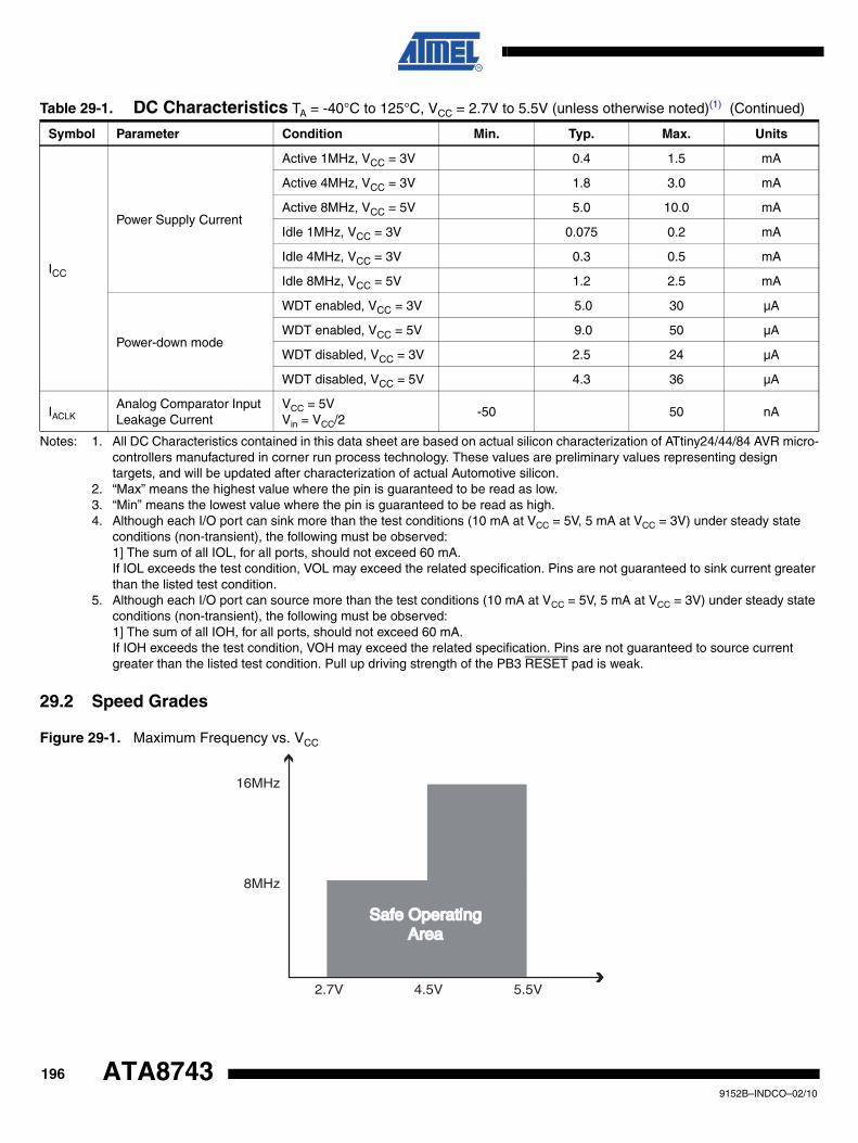
Notes: 1. All DC Characteristics contained in this data sheet are based on actual silicon characterization of ATtiny24/44/84 AVR micro-controllers manufactured in corner run process technology. These values are preliminary values representing design targets, and will be updated after characterization of actual Automotive silicon.
2. “Max” means the highest value where the pin is guaranteed to be read as low.3. “Min” means the lowest value where the pin is guaranteed to be read as high.4. Although each I/O port can sink more than the test conditions (10 mA at VCC = 5V, 5 mA at VCC = 3V) under steady state
conditions (non-transient), the following must be observed:1] The sum of all IOL, for all ports, should not exceed 60 mA.If IOL exceeds the test condition, VOL may exceed the related specification. Pins are not guaranteed to sink current greater than the listed test condition.
5. Although each I/O port can source more than the test conditions (10 mA at VCC = 5V, 5 mA at VCC = 3V) under steady state conditions (non-transient), the following must be observed:1] The sum of all IOH, for all ports, should not exceed 60 mA.If IOH exceeds the test condition, VOH may exceed the related specification. Pins are not guaranteed to source current greater than the listed test condition. Pull up driving strength of the PB3 RESET pad is weak.
29.2 Speed Grades
Figure 29-1. Maximum Frequency vs. VCC
ICC
Power Supply Current
Active 1MHz, VCC = 3V 0.4 1.5 mA
Active 4MHz, VCC = 3V 1.8 3.0 mA
Active 8MHz, VCC = 5V 5.0 10.0 mA
Idle 1MHz, VCC = 3V 0.075 0.2 mA
Idle 4MHz, VCC = 3V 0.3 0.5 mA
Idle 8MHz, VCC = 5V 1.2 2.5 mA
Power-down mode
WDT enabled, VCC = 3V 5.0 30 µA
WDT enabled, VCC = 5V 9.0 50 µA
WDT disabled, VCC = 3V 2.5 24 µA
WDT disabled, VCC = 5V 4.3 36 µA
IACLKAnalog Comparator Input Leakage Current
VCC = 5VVin = VCC/2
-50 50 nA
Table 29-1. DC Characteristics TA = -40°C to 125°C, VCC = 2.7V to 5.5V (unless otherwise noted)(1) (Continued)
Symbol Parameter Condition Min. Typ. Max. Units
2.7V
8MHz
16MHz
4.5V 5.5V
Safe OperatingSafe OperatingAreaArea
1969152B–INDCO–02/10
ATA8743
ATA8743
29.3 Clock Characterizations
29.3.1 Calibrated Internal RC Oscillator Accuracy
Note: 1. The overall jitter increase proportionally to the divider ratio
Example: with Oscillator divided by 32, jitter standard deviation will be 32 x 0.4 ns = 12.8 ns.
29.3.2 External Clock Drive Waveforms
Figure 29-2. External Clock Drive Waveforms
29.3.3 External Clock Drive
Table 29-2. Calibration Accuracy of Internal RC Oscillator
Frequency VCC Temperature Accuracy
FactoryCalibration
8.0 MHz 3V 25°C ±2%
User Calibration 7.3 - 8.1 MHz 2.7V - 5.5V -40°C - 125°C ±20%
Oscillator Jitter 8.0 MHz 2.7V - 5.5V -40°C - 125° Standard Deviation 0.4 ns(1)
VIL1
VIH1
Table 29-3. External Clock Drive
Symbol Parameter
VCC = 2.7 - 5.5V VCC = 4.5 - 5.5V
UnitsMin. Max. Min. Max.
1/tCLCL Clock Frequency 0 10 0 20 MHz
tCLCL Clock Period 100 50 ns
tCHCX High Time 40 20 ns
tCLCX Low Time 40 20 ns
tCLCH Rise Time 1.6 0.5 µs
tCHCL Fall Time 1.6 0.5 µs
ΔtCLCL Change in period from one clock cycle to the next 2 2 %
1979152B–INDCO–02/10
29.4 System and Reset Characterizations
Notes: 1. Values are guidelines only.2. This is the limit to which VDD can be lowered without losing RAM data
Note: 1. VBOT may be below nominal minimum operating voltage for some devices. For devices where this is the case, the device is tested down to VCC = VBOT during the production test. This guar-antees that a Brown-out Reset will occur before VCC drops to a voltage where correct operation of the microcontroller is no longer guaranteed.
29.5 ADC Characteristics – Preliminary Data
Table 29-4. Reset, Brown-out and Internal Voltage Reference Characteristics(1)
Symbol Parameter Condition Min Typ Max Units
VHYST Brown-out Detector Hysteresis 100 250 mV
VRAM2. RAM Retention Voltage(1) 50 mV
tBOD Min Pulse Width on Brown-out Reset 2 ns
VBG Bandgap reference voltage VC C= 2.7V, TA = 25°C 1.0 1.1 1.2 V
tBG Bandgap reference start-up time VC C= 2.7V, TA = 25°C 40 70 µs
IBG Bandgap reference current consumption VC C= 2.7V, TA = 25°C 10 µA
Table 29-5. BODLEVEL Fuse Coding(1)
BODLEVEL [2..0] Fuses Min VBOT Typ VBOT Max VBOT Units
111 BOD Disabled
110 1.8
V
101 2.7
100 4.3
011 2.3
010 2.2
001 1.9
000 2.0
Table 29-6. ADC Characteristics, Single Ended Channels. -40°C - 125°C
Symbol Parameter Condition Min Typ Max Units
Resolution Single Ended Conversion 10 Bits
TUEAbsolute accuracy (Including INL, DNL, quantization error, gain and offset error)
Single Ended ConversionVREF = 4V, VCC = 4V,ADC clock = 200 kHz
2.0 4.0 LSB
Single Ended ConversionVREF = 4V, VCC = 4V,ADC clock = 200 kHz
Noise Reduction Mode
2.0 4.0 LSB
1989152B–INDCO–02/10
ATA8743
ATA8743
INL Integral Non-linearity (INL)Single Ended ConversionVREF = 4V, VCC = 4V,ADC clock = 200 kHz
0.5 1.5 LSB
DNLDifferential Non-linearity (DNL)
Single Ended ConversionVREF = 4V, VCC = 4V,ADC clock = 200 kHz
0.3 0.7 LSB
Gain ErrorSingle Ended ConversionVREF = 4V, VCC = 4V,ADC clock = 200 kHz
-5.0 -3.0 5.0 LSB
Offset ErrorSingle Ended ConversionVREF = 4V, VCC = 4V,ADC clock = 200 kHz
-3.5 1.5 3.5 LSB
Conversion Time Free Running Conversion 65 260 µs
Clock Frequency 50 200 kHz
Vref External Voltage Reference 2.56 AVCC V
VIN Input Voltage GND VREF V
VINT Internal Voltage Reference 1.0 1.1 1.2 V
RAIN Analog Input Resistance 100 MΩ
Table 29-6. ADC Characteristics, Single Ended Channels. -40°C - 125°C
Symbol Parameter Condition Min Typ Max Units
1999152B–INDCO–02/10
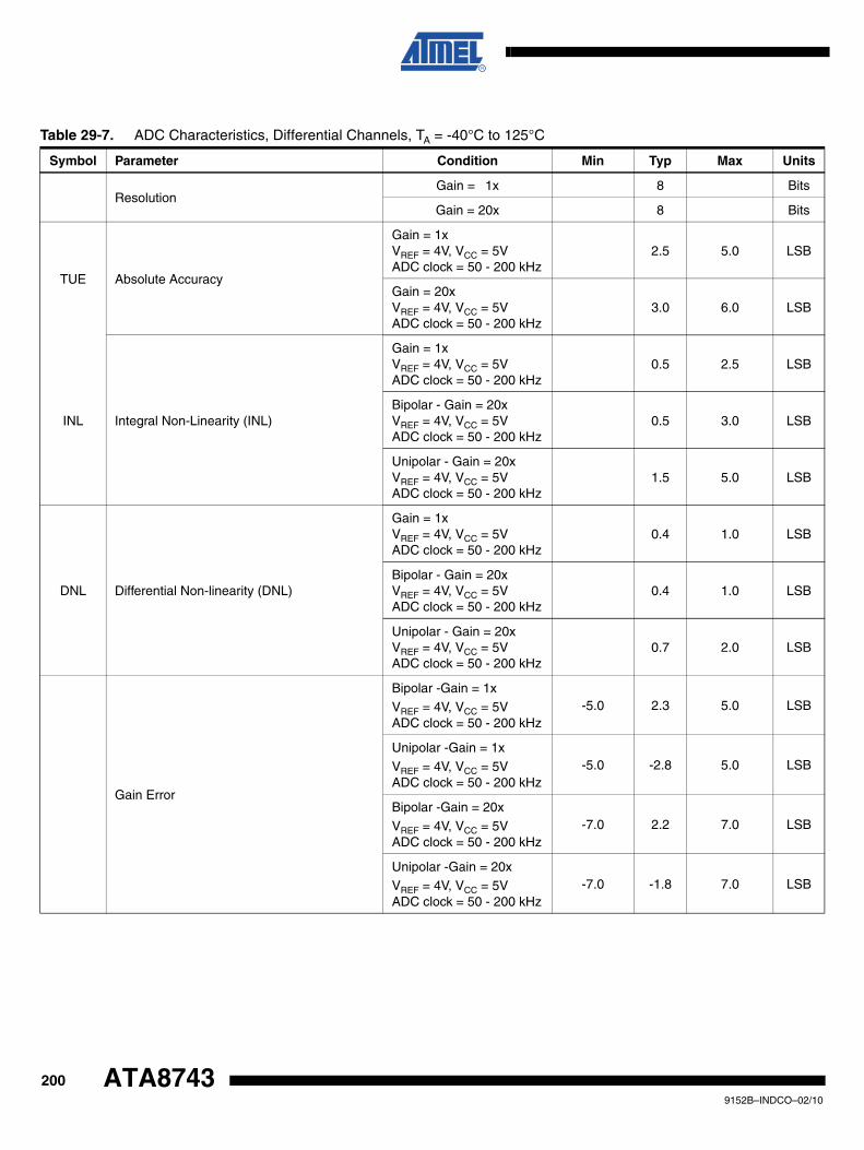
Table 29-7. ADC Characteristics, Differential Channels, TA = -40°C to 125°C
Symbol Parameter Condition Min Typ Max Units
ResolutionGain = 1x 8 Bits
Gain = 20x 8 Bits
TUE Absolute Accuracy
Gain = 1xVREF = 4V, VCC = 5VADC clock = 50 - 200 kHz
2.5 5.0 LSB
Gain = 20xVREF = 4V, VCC = 5VADC clock = 50 - 200 kHz
3.0 6.0 LSB
Integral Non-Linearity (INL)
Gain = 1xVREF = 4V, VCC = 5VADC clock = 50 - 200 kHz
0.5 2.5 LSB
INLBipolar - Gain = 20xVREF = 4V, VCC = 5VADC clock = 50 - 200 kHz
0.5 3.0 LSB
Unipolar - Gain = 20xVREF = 4V, VCC = 5VADC clock = 50 - 200 kHz
1.5 5.0 LSB
Differential Non-linearity (DNL)
Gain = 1xVREF = 4V, VCC = 5VADC clock = 50 - 200 kHz
0.4 1.0 LSB
DNLBipolar - Gain = 20xVREF = 4V, VCC = 5VADC clock = 50 - 200 kHz
0.4 1.0 LSB
Unipolar - Gain = 20xVREF = 4V, VCC = 5VADC clock = 50 - 200 kHz
0.7 2.0 LSB
Gain Error
Bipolar -Gain = 1xVREF = 4V, VCC = 5VADC clock = 50 - 200 kHz
-5.0 2.3 5.0 LSB
Unipolar -Gain = 1x
VREF = 4V, VCC = 5VADC clock = 50 - 200 kHz
-5.0 -2.8 5.0 LSB
Bipolar -Gain = 20x
VREF = 4V, VCC = 5VADC clock = 50 - 200 kHz
-7.0 2.2 7.0 LSB
Unipolar -Gain = 20xVREF = 4V, VCC = 5VADC clock = 50 - 200 kHz
-7.0 -1.8 7.0 LSB
2009152B–INDCO–02/10
ATA8743
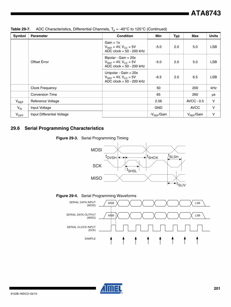
ATA8743
29.6 Serial Programming Characteristics
Figure 29-3. Serial Programming Timing
Figure 29-4. Serial Programming Waveforms
Offset Error
Gain = 1xVREF = 4V, VCC = 5VADC clock = 50 - 200 kHz
-5.0 2.0 5.0 LSB
Bipolar - Gain = 20xVREF = 4V, VCC = 5VADC clock = 50 - 200 kHz
-5.0 2.0 5.0 LSB
Unipolar - Gain = 20xVREF = 4V, VCC = 5VADC clock = 50 - 200 kHz
-6.5 2.0 6.5 LSB
Clock Frequency 50 200 kHz
Conversion Time 65 260 µs
VREF Reference Voltage 2.56 AVCC - 0.5 V
VIN Input Voltage GND AVCC V
VDIFF Input Differential Voltage -VREF/Gain VREF/Gain V
Table 29-7. ADC Characteristics, Differential Channels, TA = -40°C to 125°C (Continued)
Symbol Parameter Condition Min Typ Max Units
MOSI
MISO
SCK
tOVSH
tSHSL
tSLSHtSHOX
tSLIV
MSB
MSB
LSB
LSB
SERIAL CLOCK INPUT(SCK)
SERIAL DATA INPUT (MOSI)
(MISO)
SAMPLE
SERIAL DATA OUTPUT
2019152B–INDCO–02/10
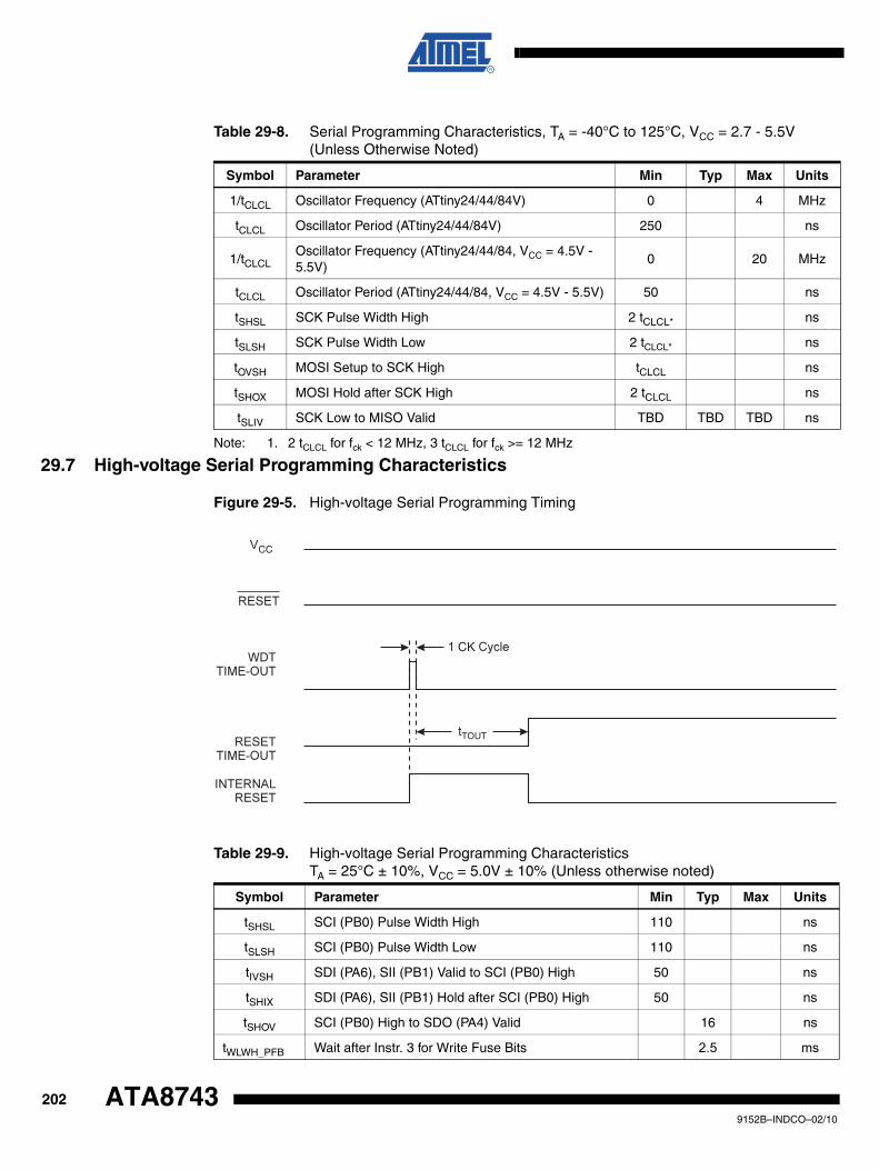
Note: 1. 2 tCLCL for fck < 12 MHz, 3 tCLCL for fck >= 12 MHz
29.7 High-voltage Serial Programming Characteristics
Figure 29-5. High-voltage Serial Programming Timing
Table 29-8. Serial Programming Characteristics, TA = -40°C to 125°C, VCC = 2.7 - 5.5V (Unless Otherwise Noted)
Symbol Parameter Min Typ Max Units
1/tCLCL Oscillator Frequency (ATtiny24/44/84V) 0 4 MHz
tCLCL Oscillator Period (ATtiny24/44/84V) 250 ns
1/tCLCLOscillator Frequency (ATtiny24/44/84, VCC = 4.5V - 5.5V)
0 20 MHz
tCLCL Oscillator Period (ATtiny24/44/84, VCC = 4.5V - 5.5V) 50 ns
tSHSL SCK Pulse Width High 2 tCLCL* ns
tSLSH SCK Pulse Width Low 2 tCLCL* ns
tOVSH MOSI Setup to SCK High tCLCL ns
tSHOX MOSI Hold after SCK High 2 tCLCL ns
tSLIV SCK Low to MISO Valid TBD TBD TBD ns
Table 29-9. High-voltage Serial Programming Characteristics TA = 25°C ± 10%, VCC = 5.0V ± 10% (Unless otherwise noted)
Symbol Parameter Min Typ Max Units
tSHSL SCI (PB0) Pulse Width High 110 ns
tSLSH SCI (PB0) Pulse Width Low 110 ns
tIVSH SDI (PA6), SII (PB1) Valid to SCI (PB0) High 50 ns
tSHIX SDI (PA6), SII (PB1) Hold after SCI (PB0) High 50 ns
tSHOV SCI (PB0) High to SDO (PA4) Valid 16 ns
tWLWH_PFB Wait after Instr. 3 for Write Fuse Bits 2.5 ms
CK
CC
2029152B–INDCO–02/10
ATA8743

ATA8743
2039152B–INDCO–02/10
30. Typical Characteristics – Preliminary Data
The data contained in this section is largely based on simulations and characterization of similardevices in the same process and design methods. Thus, the data should be treated as indica-tions of how the part will behave.
The following charts show typical behavior. These figures are not tested during manufacturing.All current consumption measurements are performed with all I/O pins configured as inputs andwith internal pull-ups enabled. A sine wave generator with rail-to-rail output is used as clocksource.
The power consumption in Power-down mode is independent of clock selection.
The current consumption is a function of several factors such as: operating voltage, operatingfrequency, loading of I/O pins, switching rate of I/O pins, code executed and ambient tempera-ture. The dominating factors are operating voltage and frequency.
The current drawn from capacitive loaded pins may be estimated (for one pin) as CL*VCC*f whereCL = load capacitance, VCC = operating voltage and f = average switching frequency of I/O pin.
The parts are characterized at frequencies higher than test limits. Parts are not guaranteed tofunction properly at frequencies higher than the ordering code indicates.
The difference between current consumption in Power-down mode with Watchdog Timerenabled and Power-down mode with Watchdog Timer disabled represents the differential cur-rent drawn by the Watchdog Timer.
30.1 Active Supply Current
Figure 30-1. Active Supply Current vs. Low Frequency (0.1 - 1.0 MHz) - Temp.=25°C
Figure 30-2. Active Supply Current vs. Low Frequency (0.1 - 1.0 MHz) - Temp.=125°C
ACTIVE SUPPLY CURRENT vs . LOW FREQUENCY0.1 - 1.0 MHz - Temperature = 25˚C
5.5 V
5.0 V
4.5 V
3.3 V3.0 V2.7 V
0
0.2
0.4
0.6
0.8
1
1.2
0 0.1 0.2 0.3 0.4 0.5 0.6 0.7 0.8 0.9 1
Frequency (MHz)
I CC (
mA
)
2049152B–INDCO–02/10
ATA8743
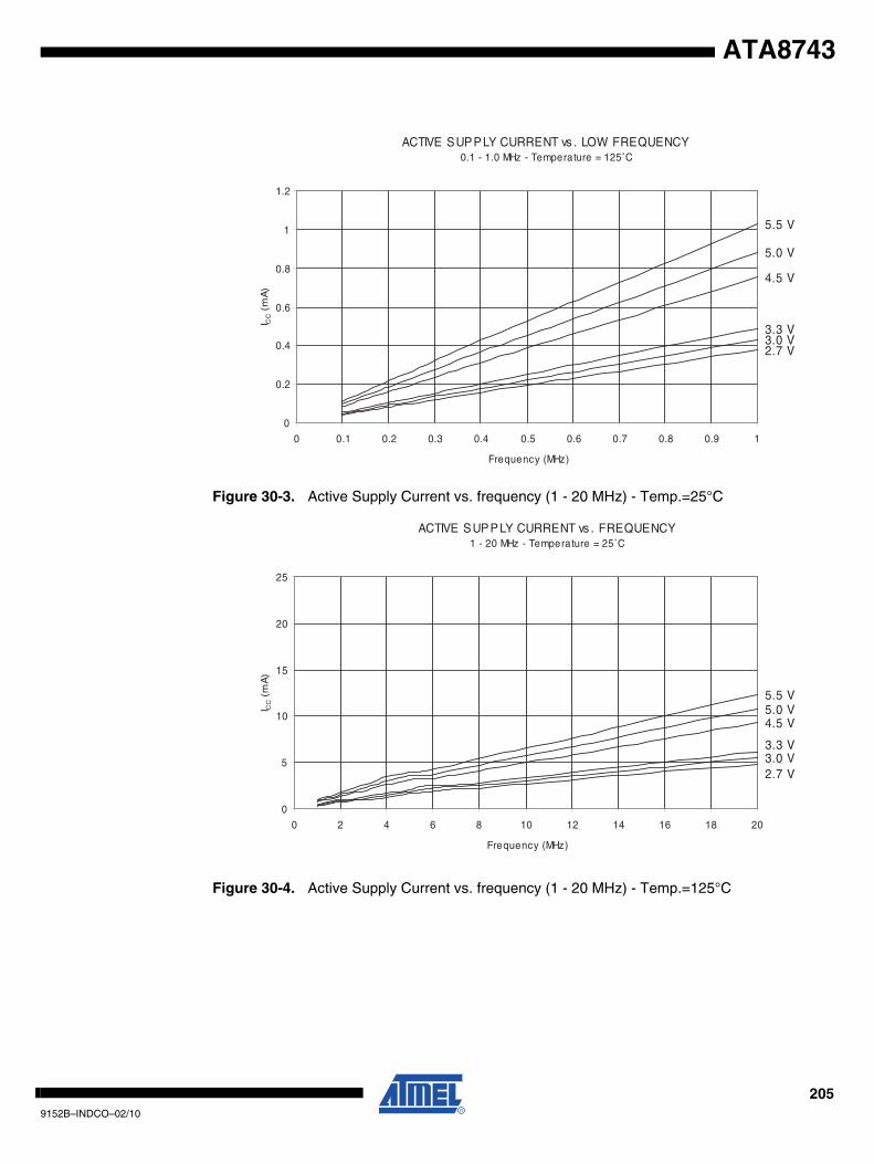
ATA8743
Figure 30-3. Active Supply Current vs. frequency (1 - 20 MHz) - Temp.=25°C
Figure 30-4. Active Supply Current vs. frequency (1 - 20 MHz) - Temp.=125°C
ACTIVE SUPPLY CURRENT vs . LOW FREQUENCY0.1 - 1.0 MHz - Temperature = 125˚C
5.5 V
5.0 V
4.5 V
3.3 V3.0 V2.7 V
0
0.2
0.4
0.6
0.8
1
1.2
0 0.1 0.2 0.3 0.4 0.5 0.6 0.7 0.8 0.9 1
Frequency (MHz)
I CC (
mA
)
ACTIVE SUPPLY CURRENT vs . FREQUENCY1 - 20 MHz - Temperature = 25˚C
5.5 V5.0 V4.5 V
3.3 V3.0 V2.7 V
0
5
10
15
20
25
0 2 4 6 8 10 12 14 16 18 20
Frequency (MHz)
I CC (
mA
)
2059152B–INDCO–02/10
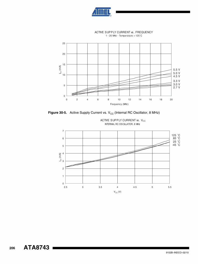
Figure 30-5. Active Supply Current vs. VCC (Internal RC Oscillator, 8 MHz)
ACTIVE SUPPLY CURRENT vs . FREQUENCY1 - 20 MHz - Temperature = 125˚C
5.5 V5.0 V4.5 V
3.3 V3.0 V2.7 V
0
5
10
15
20
25
0 2 4 6 8 10 12 14 16 18 20
Frequency (MHz)
I CC (
mA
)
ACTIVE SUPPLY CURRENT vs . VCC
INTERNAL RC OSCILLATOR, 8 MHz
125 ˚C85 ˚C25 ˚C
-45 ˚C
0
1
2
3
4
5
6
7
2.5 3 3.5 4 4.5 5 5.5
VCC (V)
I CC (
mA
)
2069152B–INDCO–02/10
ATA8743
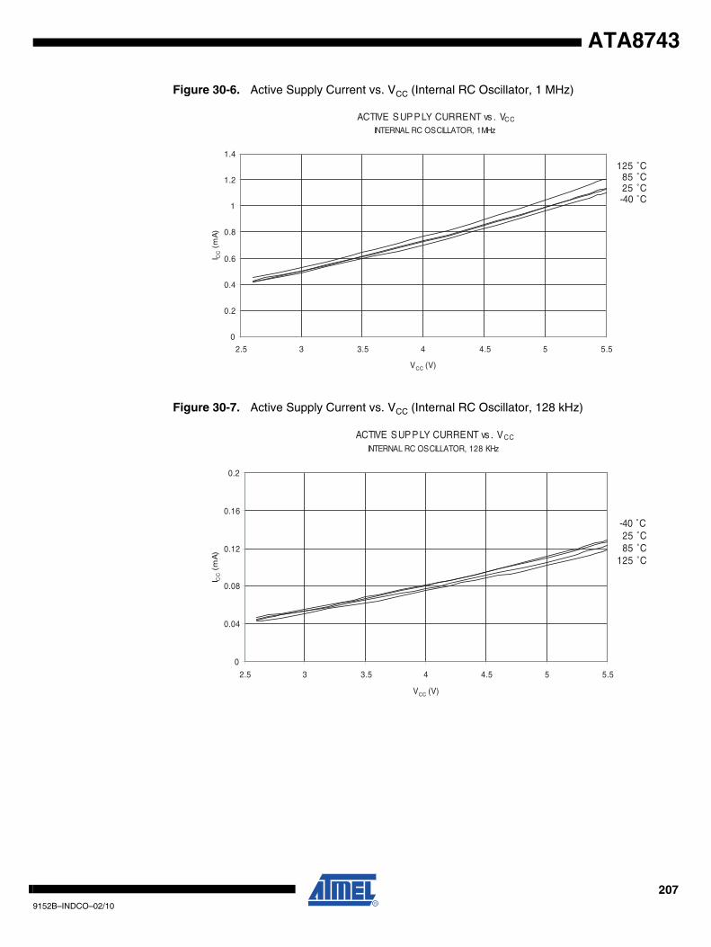
ATA8743
Figure 30-6. Active Supply Current vs. VCC (Internal RC Oscillator, 1 MHz)
Figure 30-7. Active Supply Current vs. VCC (Internal RC Oscillator, 128 kHz)
ACTIVE SUPPLY CURRENT vs . VCC
INTERNAL RC OSCILLATOR, 1MHz
125 ˚C85 ˚C25 ˚C-40 ˚C
0
0.2
0.4
0.6
0.8
1
1.2
1.4
2.5 3 3.5 4 4.5 5 5.5
VCC (V)
I CC (
mA
)
ACTIVE SUPPLY CURRENT vs . VCC
INTERNAL RC OSCILLATOR, 128 KHz
125 ˚C85 ˚C25 ˚C
-40 ˚C
0
0.04
0.08
0.12
0.16
0.2
2.5 3 3.5 4 4.5 5 5.5
VCC (V)
I CC (
mA
)
2079152B–INDCO–02/10
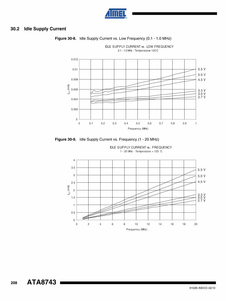
30.2 Idle Supply Current
Figure 30-8. Idle Supply Current vs. Low Frequency (0.1 - 1.0 MHz)
Figure 30-9. Idle Supply Current vs. Frequency (1 - 20 MHz)
IDLE SUPPLY CURRENT vs . LOW FREQUENCY0.1 - 1.0 MHz - Temperature = 125̊ C
5.5 V
5.0 V
4.5 V
3.3 V3.0 V2.7 V
0
0.002
0.004
0.006
0.008
0.01
0.012
0 0.1 0.2 0.3 0.4 0.5 0.6 0.7 0.8 0.9 1
Frequency (MHz)
I CC (
mA
)
IDLE SUPPLY CURRENT vs . FREQUENCY1 - 20 MHz - Temperature = 125 ˚C
5.5 V
5.0 V
4.5 V
3.3 V3.0 V2.7 V
0
0.5
1
1.5
2
2.5
3
3.5
4
0 2 4 6 8 10 12 14 16 18 20
Frequency (MHz)
I CC (
mA
)
2089152B–INDCO–02/10
ATA8743
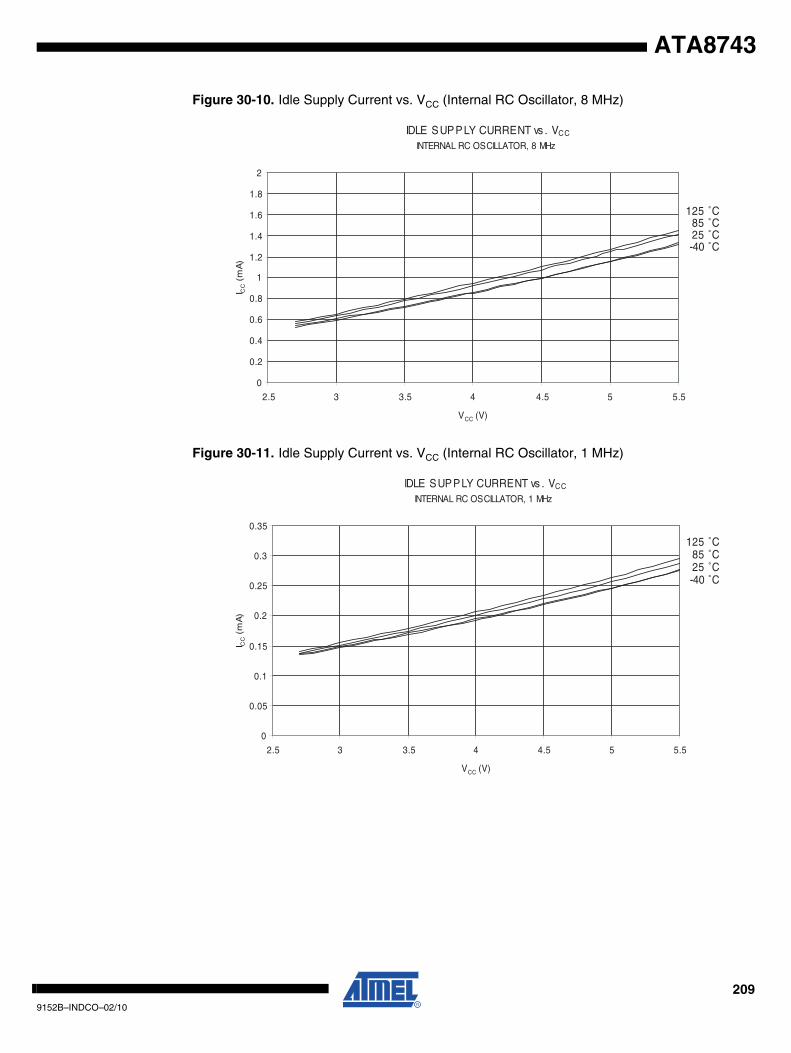
ATA8743
Figure 30-10. Idle Supply Current vs. VCC (Internal RC Oscillator, 8 MHz)
Figure 30-11. Idle Supply Current vs. VCC (Internal RC Oscillator, 1 MHz)
IDLE SUPPLY CURRENT vs . VCC
INTERNAL RC OSCILLATOR, 8 MHz
125 ˚C85 ˚C25 ˚C-40 ˚C
0
0.2
0.4
0.6
0.8
1
1.2
1.4
1.6
1.8
2
2.5 3 3.5 4 4.5 5 5.5
VCC (V)
I CC (
mA
)
IDLE SUPPLY CURRENT vs . VCC
INTERNAL RC OSCILLATOR, 1 MHz
125 ˚C85 ˚C25 ˚C-40 ˚C
0
0.05
0.1
0.15
0.2
0.25
0.3
0.35
2.5 3 3.5 4 4.5 5 5.5
VCC (V)
I CC (
mA
)
2099152B–INDCO–02/10
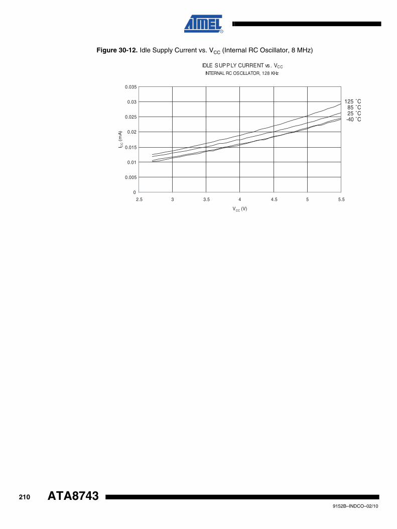
Figure 30-12. Idle Supply Current vs. VCC (Internal RC Oscillator, 8 MHz)
IDLE SUPPLY CURRENT vs . VCC
INTERNAL RC OSCILLATOR, 128 KHz
125 ˚C85 ˚C25 ˚C-40 ˚C
0
0.005
0.01
0.015
0.02
0.025
0.03
0.035
2.5 3 3.5 4 4.5 5 5.5
VCC (V)
I CC (
mA
)
2109152B–INDCO–02/10
ATA8743
ATA8743
30.3 Supply Current of IO modules
The tables and formulas below can be used to calculate the additional current consumption forthe different I/O modules in Active and Idle mode. The enabling or disabling of the I/O modulesare controlled by the Power Reduction Register. See “Power Reduction Register” on page 51 fordetails.
Table 30-1. Additional Current Consumption for the different I/O modules (absolute values)
PRR bit Typical numbers
VCC = 2V, F = 1MHz VCC = 3V, F = 4MHz VCC = 5V, F = 8MHz
PRTIM1 6.6 uA 26 uA 106 uA
PRTIM0 8.7uA 35 uA 140 uA
PRUSI 5.5 uA 22 uA 87 uA
PRADC 22 uA 87 uA 340 uA
2119152B–INDCO–02/10
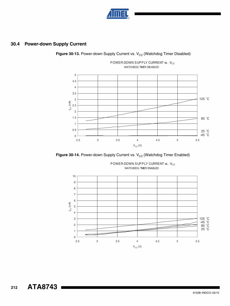
30.4 Power-down Supply Current
Figure 30-13. Power-down Supply Current vs. VCC (Watchdog Timer Disabled)
Figure 30-14. Power-down Supply Current vs. VCC (Watchdog Timer Enabled)
POWER-DOWN SUPPLY CURRENT vs . VCC
WATCHDOG TIMER DISABLED
125 ˚C
85 ˚C
25 ˚C-45 ˚C0
0.5
1
1.5
2
2.5
3
3.5
4
4.5
5
2.5 3 3.5 4 4.5 5 5.5
VCC (V)
I CC (
uA
)
POWER-DOWN SUPPLY CURRENT vs . VCC
WATCHDOG TIMER ENABLED
125 ˚C
85 ˚C25 ˚C
-45 ˚C
0
1
2
3
4
5
6
7
8
9
10
2.5 3 3.5 4 4.5 5 5.5
VCC (V)
I CC (
uA
)
2129152B–INDCO–02/10
ATA8743
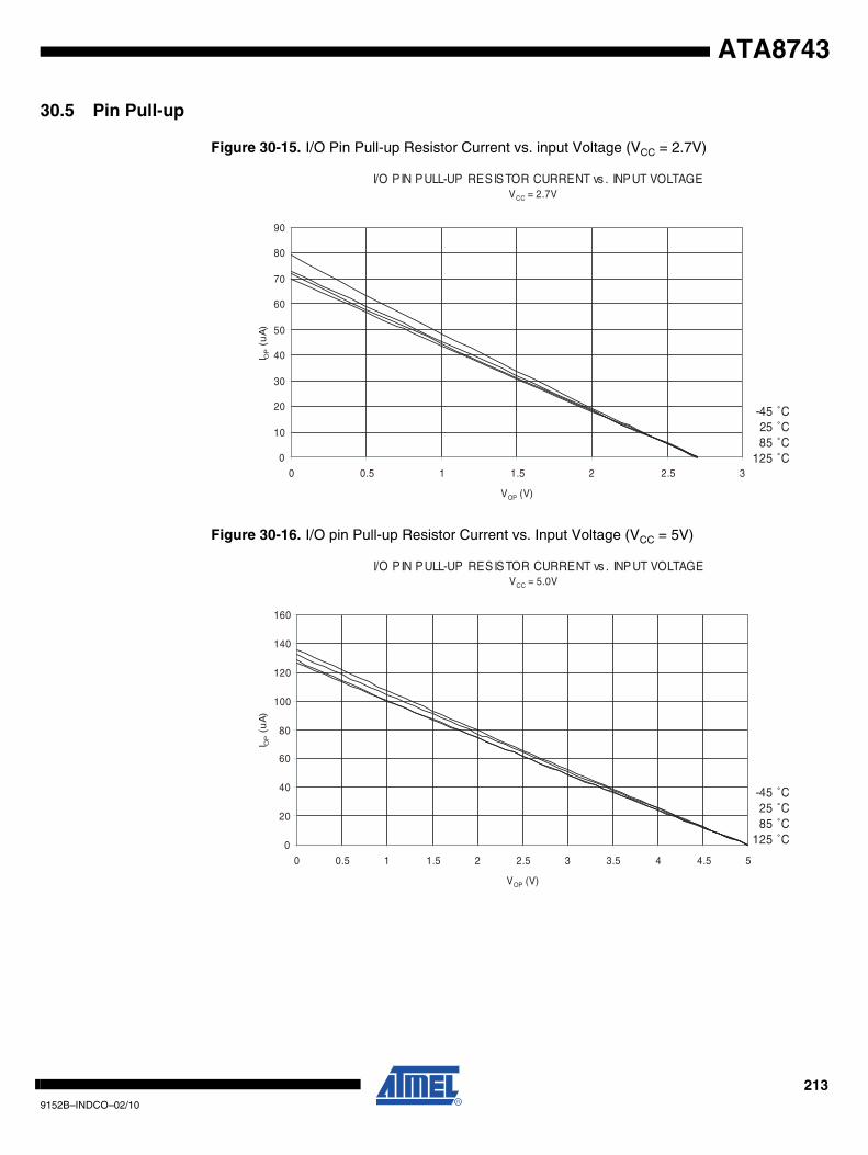
ATA8743
30.5 Pin Pull-up
Figure 30-15. I/O Pin Pull-up Resistor Current vs. input Voltage (VCC = 2.7V)
Figure 30-16. I/O pin Pull-up Resistor Current vs. Input Voltage (VCC = 5V)
I/O P IN PULL-UP RESISTOR CURRENT vs . INPUT VOLTAGEVCC = 2.7V
125 ˚C85 ˚C25 ˚C
-45 ˚C
0
10
20
30
40
50
60
70
80
90
0 0.5 1 1.5 2 2.5 3
VOP (V)
I OP (
uA
)
I/O P IN PULL-UP RESISTOR CURRENT vs . INPUT VOLTAGEVCC = 5.0V
125 ˚C85 ˚C25 ˚C
-45 ˚C
0
20
40
60
80
100
120
140
160
0 0.5 1 1.5 2 2.5 3 3.5 4 4.5 5
VOP (V)
I OP (
uA
)
2139152B–INDCO–02/10
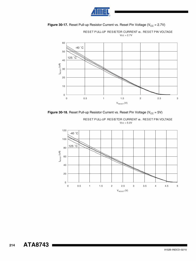
Figure 30-17. Reset Pull-up Resistor Current vs. Reset Pin Voltage (VCC = 2.7V)
Figure 30-18. Reset Pull-up Resistor Current vs. Reset Pin Voltage (VCC = 5V)
RESET PULL-UP RESISTOR CURRENT vs . RESET P IN VOLTAGEVcc = 2.7V
125 ˚C
-40 ˚C
0
10
20
30
40
50
60
0 0.5 1 1.5 2 2.5 3
VRES ET (V)
I RE
SE
T (u
A)
RESET PULL-UP RESISTOR CURRENT vs . RESET P IN VOLTAGEVcc = 5.0V
125 ˚C
-40 ˚C
0
20
40
60
80
100
120
0 0.5 1 1.5 2 2.5 3 3.5 4 4.5 5
VRES ET (V)
I RE
SE
T (u
A)
2149152B–INDCO–02/10
ATA8743
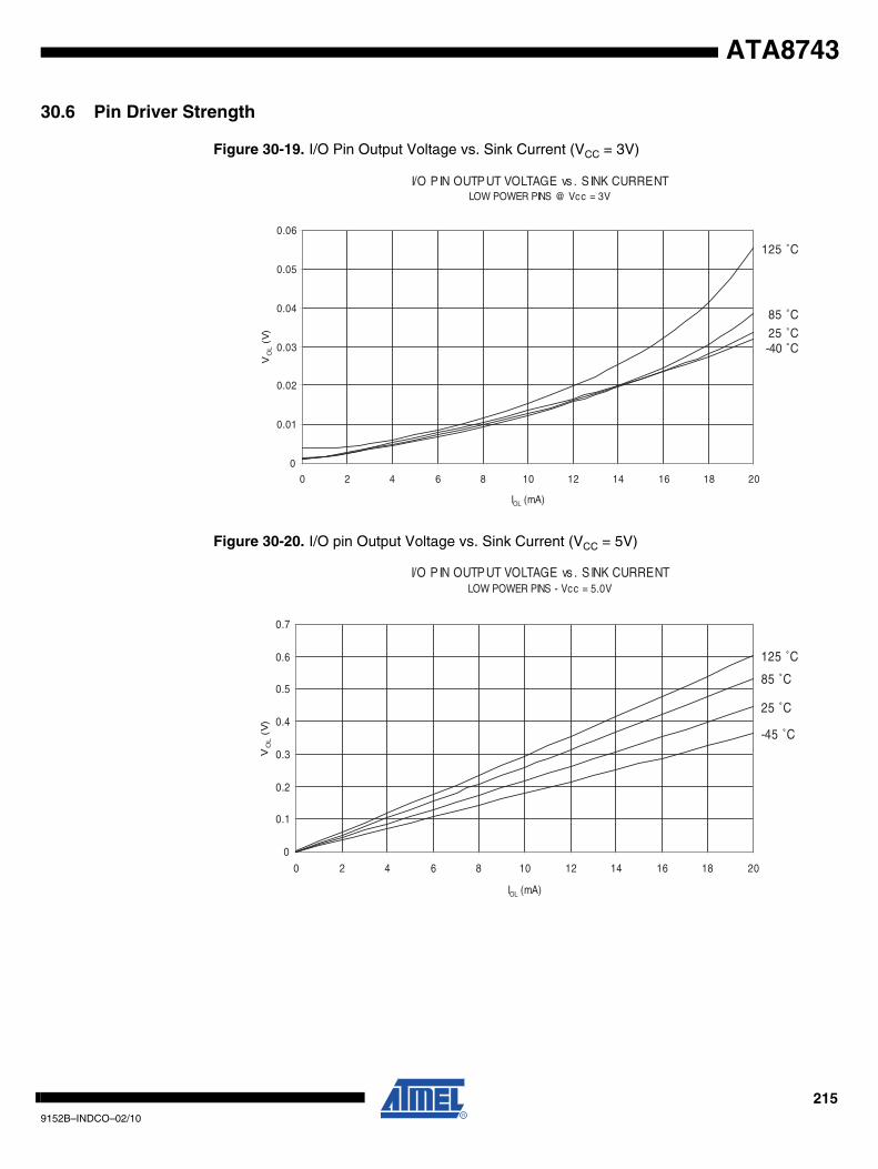
ATA8743
30.6 Pin Driver Strength
Figure 30-19. I/O Pin Output Voltage vs. Sink Current (VCC = 3V)
Figure 30-20. I/O pin Output Voltage vs. Sink Current (VCC = 5V)
I/O P IN OUTPUT VOLTAGE vs . S INK CURRENTLOW POWER PINS @ Vcc = 3V
125 ˚C
85 ˚C
25 ˚C-40 ˚C
0
0.01
0.02
0.03
0.04
0.05
0.06
0 2 4 6 8 10 12 14 16 18 20
IOL (mA)
VO
L (V
)
I/O P IN OUTPUT VOLTAGE vs . S INK CURRENTLOW POWER PINS - Vcc = 5.0V
125 ˚C
85 ˚C
25 ˚C
-45 ˚C
0
0.1
0.2
0.3
0.4
0.5
0.6
0.7
0 2 4 6 8 10 12 14 16 18 20
IOL (mA)
VO
L (
V)
2159152B–INDCO–02/10
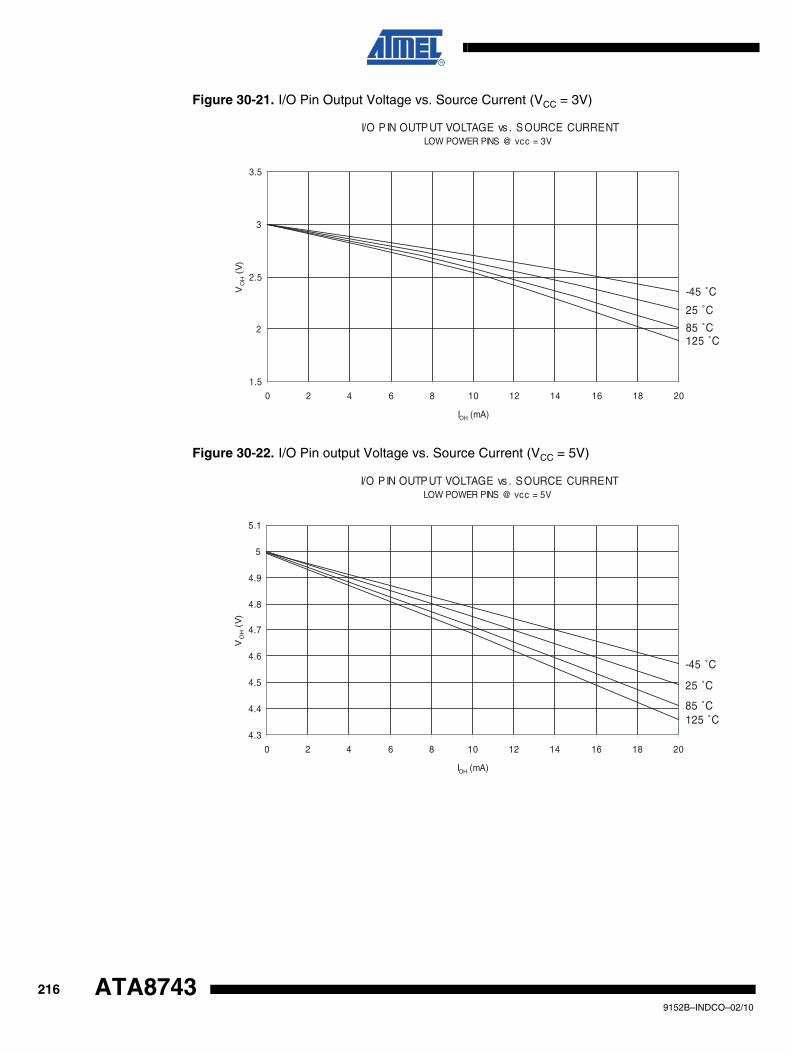
Figure 30-21. I/O Pin Output Voltage vs. Source Current (VCC = 3V)
Figure 30-22. I/O Pin output Voltage vs. Source Current (VCC = 5V)
I/O P IN OUTPUT VOLTAGE vs . SOURCE CURRENTLOW POWER PINS @ vcc = 3V
125 ˚C85 ˚C
25 ˚C
-45 ˚C
1.5
2
2.5
3
3.5
0 2 4 6 8 10 12 14 16 18 20
IOH (mA)
VO
H (
V)
I/O P IN OUTPUT VOLTAGE vs . SOURCE CURRENTLOW POWER PINS @ vcc = 5V
125 ˚C85 ˚C
25 ˚C
-45 ˚C
4.3
4.4
4.5
4.6
4.7
4.8
4.9
5
5.1
0 2 4 6 8 10 12 14 16 18 20
IOH (mA)
VO
H (
V)
2169152B–INDCO–02/10
ATA8743
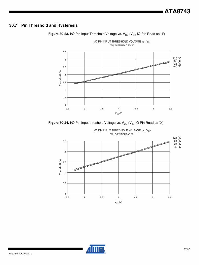
ATA8743
30.7 Pin Threshold and Hysteresis
Figure 30-23. I/O Pin Input Threshold Voltage vs. VCC (VIH, IO Pin Read as ‘1’)
Figure 30-24. I/O Pin Input threshold Voltage vs. VCC (VIL, IO Pin Read as ‘0’)
I/O P IN INPUT THRESHOLD VOLTAGE vs . VCC
VIH, IO PIN READ AS '1'
125 ˚C85 ˚C25 ˚C
-40 ˚C
0
0.5
1
1.5
2
2.5
3
3.5
2.5 3 3.5 4 4.5 5 5.5
VCC (V)
Th
res
ho
ld (
V)
I/O P IN INPUT THRESHOLD VOLTAGE vs . VCC
VIL, IO PIN READ AS '0'
125 ˚C85 ˚C25 ˚C-40 ˚C
0
0.5
1
1.5
2
2.5
2.5 3 3.5 4 4.5 5 5.5
VCC (V)
Th
res
ho
ld (
V)
2179152B–INDCO–02/10
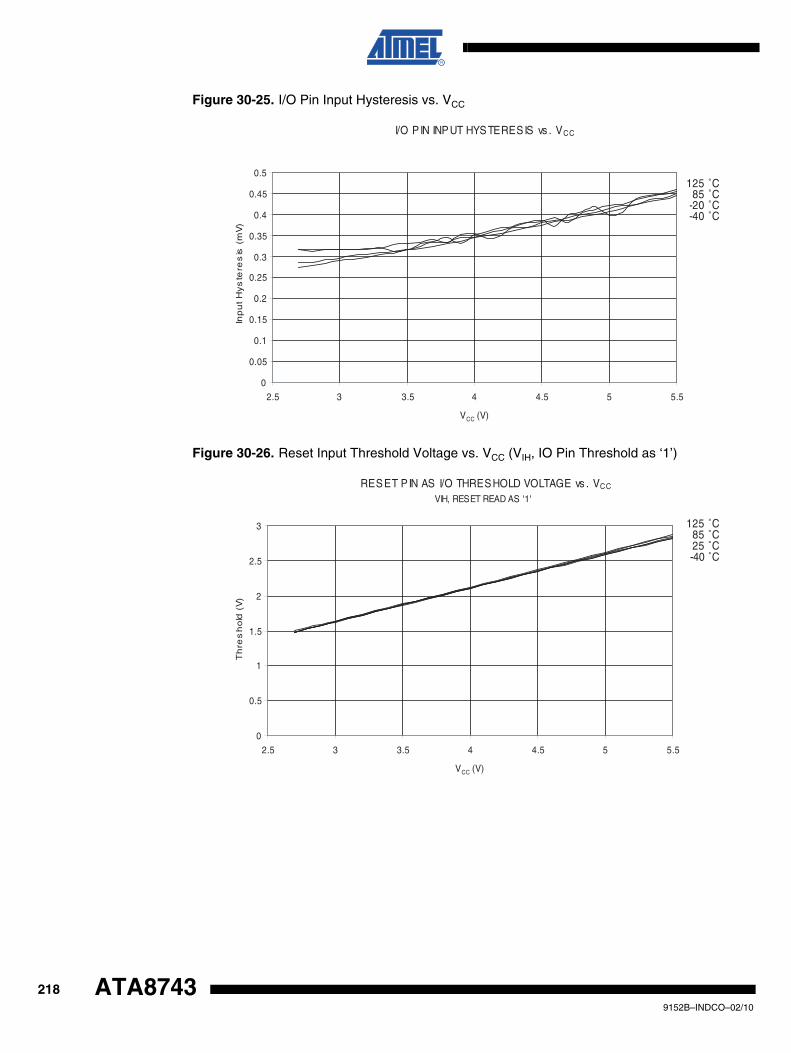
Figure 30-25. I/O Pin Input Hysteresis vs. VCC
Figure 30-26. Reset Input Threshold Voltage vs. VCC (VIH, IO Pin Threshold as ‘1’)
I/O P IN INPUT HYSTERESIS vs . VCC
125 ˚C85 ˚C
-20 ˚C-40 ˚C
0
0.05
0.1
0.15
0.2
0.25
0.3
0.35
0.4
0.45
0.5
2.5 3 3.5 4 4.5 5 5.5
VCC (V)
Inp
ut
Hys
tere
sis
(m
V)
RESET P IN AS I/O THRESHOLD VOLTAGE vs . VCC
VIH, RESET READ AS '1'
125 ˚C85 ˚C25 ˚C-40 ˚C
0
0.5
1
1.5
2
2.5
3
2.5 3 3.5 4 4.5 5 5.5
VCC (V)
Th
res
ho
ld (
V)
2189152B–INDCO–02/10
ATA8743
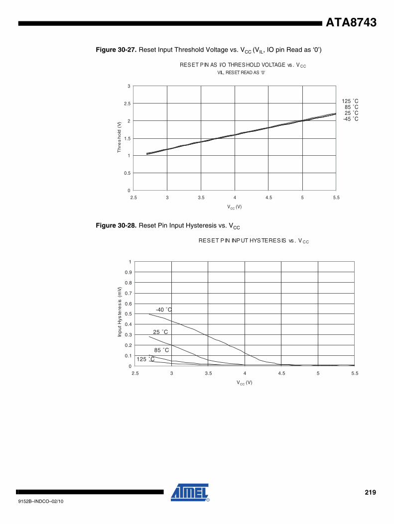
ATA8743
Figure 30-27. Reset Input Threshold Voltage vs. VCC (VIL, IO pin Read as ‘0’)
Figure 30-28. Reset Pin Input Hysteresis vs. VCC
RESET P IN AS I/O THRESHOLD VOLTAGE vs . V CC
VIL, RESET READ AS '0'
125 ˚C85 ˚C25 ˚C
-45 ˚C
0
0.5
1
1.5
2
2.5
3
2.5 3 3.5 4 4.5 5 5.5
VCC (V)
Th
res
ho
ld (
V)
RESET P IN INPUT HYSTERESIS vs . V CC
125 ˚C
85 ˚C
25 ˚C
-40 ˚C
0
0.1
0.2
0.3
0.4
0.5
0.6
0.7
0.8
0.9
1
2.5 3 3.5 4 4.5 5 5.5
VCC (V)
Inp
ut
Hys
tere
sis
(m
V)
2199152B–INDCO–02/10
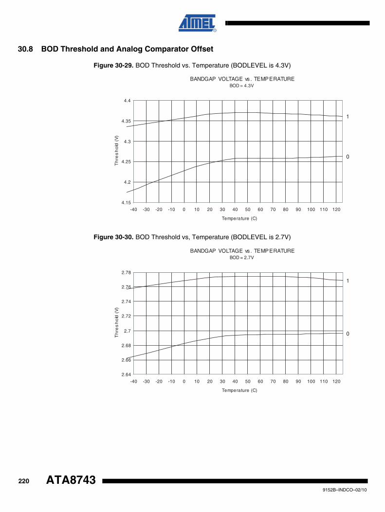
30.8 BOD Threshold and Analog Comparator Offset
Figure 30-29. BOD Threshold vs. Temperature (BODLEVEL is 4.3V)
Figure 30-30. BOD Threshold vs, Temperature (BODLEVEL is 2.7V)
BANDGAP VOLTAGE vs . TEMPERATUREBOD = 4.3V
1
0
4.15
4.2
4.25
4.3
4.35
4.4
-40 -30 -20 -10 0 10 20 30 40 50 60 70 80 90 100 110 120
Temperature (C)
Th
res
ho
ld (
V)
BANDGAP VOLTAGE vs . TEMPERATUREBOD = 2.7V
1
0
2.64
2.66
2.68
2.7
2.72
2.74
2.76
2.78
-40 -30 -20 -10 0 10 20 30 40 50 60 70 80 90 100 110 120
Temperature (C)
Th
res
ho
ld (
V)
2209152B–INDCO–02/10
ATA8743
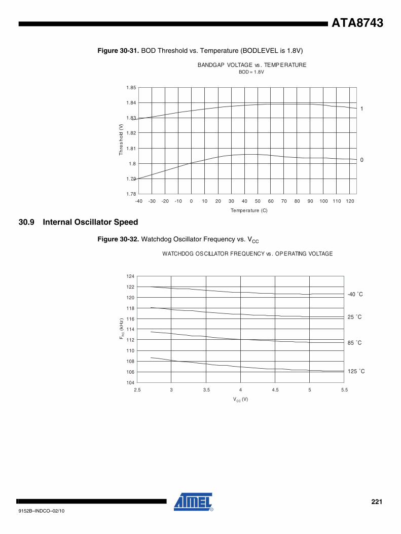
ATA8743
Figure 30-31. BOD Threshold vs. Temperature (BODLEVEL is 1.8V)
30.9 Internal Oscillator Speed
Figure 30-32. Watchdog Oscillator Frequency vs. VCC
BANDGAP VOLTAGE vs . TEMPERATUREBOD = 1.8V
1
0
1.78
1.79
1.8
1.81
1.82
1.83
1.84
1.85
-40 -30 -20 -10 0 10 20 30 40 50 60 70 80 90 100 110 120
Temperature (C)
Th
res
ho
ld (
V)
WATCHDOG OSCILLATOR FREQUENCY vs . OPERATING VOLTAGE
125 ˚C
85 ˚C
25 ˚C
-40 ˚C
104
106
108
110
112
114
116
118
120
122
124
2.5 3 3.5 4 4.5 5 5.5
VCC (V)
FR
C (
kH
z)
2219152B–INDCO–02/10
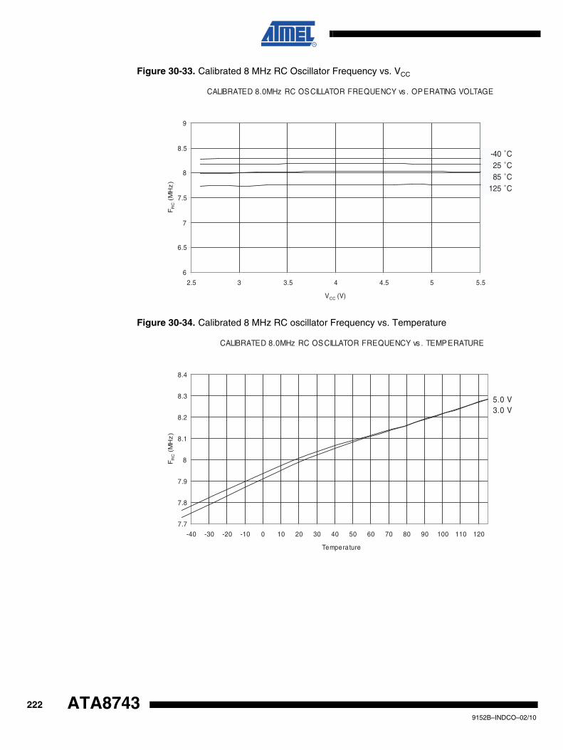
Figure 30-33. Calibrated 8 MHz RC Oscillator Frequency vs. VCC
Figure 30-34. Calibrated 8 MHz RC oscillator Frequency vs. Temperature
CALIBRATED 8.0MHz RC OSCILLATOR FREQUENCY vs . OPERATING VOLTAGE
6
6.5
7
7.5
8
8.5
9
2.5 3 3.5 4 4.5 5 5.5
VCC (V)
FR
C (
MH
z)
-40 ˚C25 ˚C85 ˚C
125 ˚C
CALIBRATED 8.0MHz RC OSCILLATOR FREQUENCY vs . TEMPERATURE
5.0 V3.0 V
7.7
7.8
7.9
8
8.1
8.2
8.3
8.4
-40 -30 -20 -10 0 10 20 30 40 50 60 70 80 90 100 110 120
Temperature
FR
C (
MH
z)
2229152B–INDCO–02/10
ATA8743
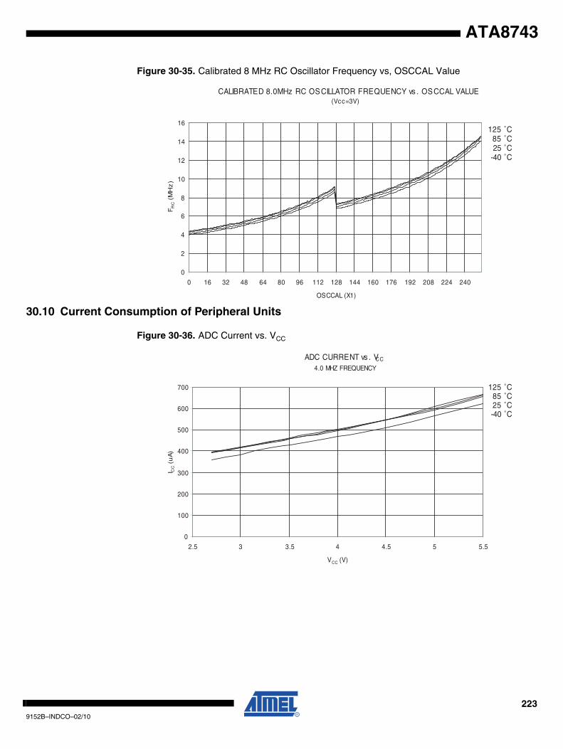
ATA8743
Figure 30-35. Calibrated 8 MHz RC Oscillator Frequency vs, OSCCAL Value
30.10 Current Consumption of Peripheral Units
Figure 30-36. ADC Current vs. VCC
CALIBRATED 8.0MHz RC OSCILLATOR FREQUENCY vs . OSCCAL VALUE(Vcc=3V)
125 ˚C85 ˚C25 ˚C
-40 ˚C
0
2
4
6
8
10
12
14
16
0 16 32 48 64 80 96 112 128 144 160 176 192 208 224 240
OSCCAL (X1)
FR
C (
MH
z)
ADC CURRENT vs . VCC
4.0 MHZ FREQUENCY
-40 ˚C25 ˚C85 ˚C
125 ˚C
0
100
200
300
400
500
600
700
2.5 3 3.5 4 4.5 5 5.5
VCC (V)
I CC (
uA
)
2239152B–INDCO–02/10
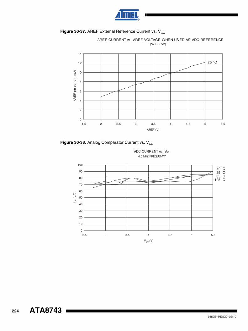
Figure 30-37. AREF External Reference Current vs. VCC
Figure 30-38. Analog Comparator Current vs. VCC
AREF CURRENT vs . AREF VOLTAGE WHEN USED AS ADC REFERENCE(Vcc=5.5V)
25 ˚C
0
2
4
6
8
10
12
14
1.5 2 2.5 3 3.5 4 4.5 5 5.5
AREF (V)
AR
EF
pin
cu
rre
nt
(uA
)
ADC CURRENT vs . VCC
4.0 MHZ FREQUENCY
-40 ˚C25 ˚C85 ˚C
125 ˚C
0
10
20
30
40
50
60
70
80
90
100
2.5 3 3.5 4 4.5 5 5.5
VCC (V)
I CC (
uA
)
2249152B–INDCO–02/10
ATA8743
ATA8743
Figure 30-39. Programming Current vs. VCC
Figure 30-40. Brownout Detector Current vs. VCC
I/O MODULE CURRENT vs . VCC4.0 MHZ FREQUENCY
25 ˚C
0
2000
4000
6000
8000
10000
12000
2.5 3.5 4.5 5.5
VCC (V)
I CC (
uA
)
BROWNOUT DETECTOR CURRENT vs . VCC
BOD level = 1.8V
125 ˚C
85 ˚C
25 ˚C
-40 ˚C0
2
4
6
8
10
12
14
16
1.5 1.6 1.7 1.8 1.9 2 2.1 2.2 2.3 2.4 2.5
VCC (V)
I CC (
uA
)
2259152B–INDCO–02/10
Figure 30-41. Watchdog Timer Current vs. VCC
30.11 Current Consumption in Reset and Reset Pulse width
Figure 30-42. Reset Supply Current vs. VCC (0.1 - 1.0 MHz, excluding Current Through the Reset Pull-up)
WATCHDOG TIMER CURRENT vs VCC
125 ˚C85 ˚C25 ˚C
-40 ˚C
0
5
10
15
20
25
30
2.5 3 3.5 4 4.5 5 5.5
VCC (V)
I CC (
uA
)
RESET SUPPLY CURRENT vs . VCC
EXCLUDING CURRENT THROUGH THE RESET PULLUP
5.5 V
5.0 V
4.5 V
3.3 V3.0 V2.7 V
0
0.02
0.04
0.06
0.08
0.1
0.12
0.14
0.16
0.18
0.2
0 0.1 0.2 0.3 0.4 0.5 0.6 0.7 0.8 0.9 1
Frequency (MHz)
I CC (
mA
)
2269152B–INDCO–02/10
ATA8743
ATA8743
Figure 30-43. Reset Supply Current vs. VCC (1 - 20 MHz, Excluding Current Through the Reset Pull-up)
Figure 30-44. Minimum Reset Pulse Width vs. VCC
RESET SUPPLY CURRENT vs . V CC
EXCLUDING CURRENT THROUGH THE RESET PULLUP
5.5 V
5.0 V
4.5 V
3.6 V3.3 V3.0 V2.7 V
0
0.5
1
1.5
2
2.5
3
0 2 4 6 8 10 12 14 16 18 20
Frequency (MHz)
I CC (
mA
)
MINIMUM RESET PULSE WIDTH vs . V CC
125 ˚C85 ˚C25 ˚C-40 ˚C
0
200
400
600
800
1000
1200
2.5 3 3.5 4 4.5 5 5.5
VCC (V)
Pu
lse
wid
th (
ns
)
2279152B–INDCO–02/10
31. Register Summary
Address Name Bit 7 Bit 6 Bit 5 Bit 4 Bit 3 Bit 2 Bit 1 Bit 0 Page
0x3F (0x5F) SREG I T H S V N Z C Page 24
0x3E (0x5E) SPH – – – – – – SP9 SP8 Page 27
0x3D (0x5D) SPL SP7 SP6 SP5 SP4 SP3 SP2 SP1 SP0 Page 27
0x3C (0x5C) OCR0B Timer/Counter0 – Output Compare Register B Page 104
0x3B (0x5B) GIMSK – INT0 PCIE1 PCIE0 – – – – Page 69
0x3A (0x5A GIFR – INTF0 PCIF1 PCIF0 – – – – Page 70
0x39 (0x59) TIMSK0 – – – – – OCIE0B OCIE0A TOIE0 Page 105
0x38 (0x58) TIFR0 – – – – OCF0B OCF0A TOV0 Page 105
0x37 (0x57) SPMCSR – – – CTPB RFLB PGWRT PGERS SPMEN Page 178
0x36 (0x56) OCR0A Timer/Counter0 – Output Compare Register A Page 104
0x35 (0x55) MCUCR – PUD SE SM1 SM0 – ISC01 ISC00 Page 69
0x34 (0x54) MCUSR – – – – WDRF BORF EXTRF PORF Page 62
0x33 (0x53) TCCR0B FOC0A FOC0B – – WGM02 CS02 CS01 CS00 Page 103
0x32 (0x52) TCNT0 Timer/Counter0 Page 104
0x31 (0x51) OSCCAL CAL7 CAL6 CAL5 CAL4 CAL3 CAL2 CAL1 CAL0 Page 48
0x30 (0x50) TCCR0A COM0A1 COM0A0 COM0B1 COM0B0 – WGM01 WGM00 Page 100
0x2F (0x4F) TCCR1A COM1A1 COM1A0 COM1B1 COM1B0 – WGM11 WGM10 Page 129
0x2E (0x4E) TCCR1B ICNC1 ICES1 – WGM13 WGM12 CS12 CS11 CS10 Page 131
0x2D (0x4D) TCNT1H Timer/Counter1 – Counter Register High Byte Page 133
0x2C (0x4C) TCNT1L Timer/Counter1 – Counter Register Low Byte Page 133
0x2B (0x4B) OCR1AH Timer/Counter1 – Compare Register A High Byte Page 133
0x2A (0x4A) OCR1AL Timer/Counter1 – Compare Register A Low Byte Page 133
0x29 (0x49) OCR1BH Timer/Counter1 – Compare Register B High Byte Page 133
0x28 (0x48) OCR1BL Timer/Counter1 – Compare Register B Low Byte Page 133
0x27 (0x47) DWDR DWDR[7:0] Page 174
0x26 (0x46) CLKPR CLKPCE – – – CLKPS3 CLKPS2 CLKPS1 CLKPS0 Page 48
0x25 (0x45) ICR1H Timer/Counter1 - Input Capture Register High Byte Page 134
0x24 (0x44) ICR1L Timer/Counter1 - Input Capture Register Low Byte Page 134
0x23 (0x43) GTCCR TSM – – – – – – PSR10 Page 137
0x22 (0x42) TCCR1C FOC1A FOC1B – – – – – – Page 132
0x21 (0x41) WDTCSR WDIF WDIE WDP3 WDCE WDE WDP2 WDP1 WDP0 Page 62
0x20 (0x40) PCMSK1 – – – – PCINT11 PCINT10 PCINT9 PCINT8 Page 70
0x1F (0x3F) EEARH – – – – – – – EEAR8 Page 38
0x1E (0x3E) EEARL EEAR7 EEAR6 EEAR5 EEAR4 EEAR3 EEAR2 EEAR1 EEAR0 Page 38
0x1D (0x3D) EEDR EEPROM Data Register Page 38
0x1C (0x3C) EECR – – EEPM1 EEPM0 EERIE EEMPE EEPE EERE Page 38
0x1B (0x3B) PORTA PORTA7 PORTA6 PORTA5 PORTA4 PORTA3 PORTA2 PORTA1 PORTA0 Page 87
0x1A (0x3A) DDRA DDA7 DDA6 DDA5 DDA4 DDA3 DDA2 DDA1 DDA0 Page 87
0x19 (0x39) PINA PINA7 PINA6 PINA5 PINA4 PINA3 PINA2 PINA1 PINA0 Page 87
0x18 (0x38) PORTB – – – – PORTB3 PORTB2 PORTB1 PORTB0 Page 87
0x17 (0x37) DDRB – – – – DDB3 DDB2 DDB1 DDB0 Page 87
0x16 (0x36) PINB – – – – PINB3 PINB2 PINB1 PINB0 Page 88
0x15 (0x35) GPIOR2 General Purpose I/O Register 2 Page 40
0x14 (0x34) GPIOR1 General Purpose I/O Register 1 Page 40
0x13 (0x33) GPIOR0 General Purpose I/O Register 0 Page 40
0x12 (0x32) PCMSK0 PCINT7 PCINT6 PCINT5 PCINT4 PCINT3 PCINT2 PCINT1 PCINT0 Page 71
0x11 (0x31)) Reserved –
0x10 (0x30) USIBR USI Buffer Register Page 146
0x0F (0x2F) USIDR USI Data Register Page 146
0x0E (0x2E) USISR USISIF USIOIF USIPF USIDC USICNT3 USICNT2 USICNT1 USICNT0 Page 146
0x0D (0x2D) USICR USISIE USIOIE USIWM1 USIWM0 USICS1 USICS0 USICLK USITC Page 147
0x0C (0x2C) TIMSK1 – – ICIE1 – – OCIE1B OCIE1A TOIE1 Page 134
0x0B (0x2B) TIFR1 – – ICF1 – – OCF1B OCF1A TOV1 Page 135
0x0A (0x2A) Reserved –
0x09 (0x29) Reserved –
0x08 (0x28) ACSR ACD ACBG ACO ACI ACIE ACIC ACIS1 ACIS0 Page 152
0x07 (0x27) ADMUX REFS1 REFS0 MUX5 MUX4 MUX3 MUX2 MUX1 MUX0 Page 166
0x06 (0x26) ADCSRA ADEN ADSC ADATE ADIF ADIE ADPS2 ADPS1 ADPS0 Page 169
0x05 (0x25) ADCH ADC Data Register High Byte Page 170
0x04 (0x24) ADCL ADC Data Register Low Byte Page 170
0x03 (0x23) ADCSRB BIN ACME – ADLAR – ADTS2 ADTS1 ADTS0 Page 171
0x02 (0x22) Reserved –
0x01 (0x21) DIDR0 ADC7D ADC6D ADC5D ADC4D ADC3D ADC2D ADC1D ADC0D Page 153,Page 172
0x00 (0x20) PRR – – – – PRTIM1 PRTIM0 PRUSI PRADC Page 51
2289152B–INDCO–02/10
ATA8743

ATA8743
Note: 1. For compatibility with future devices, reserved bits should be written to zero if accessed. Reserved I/O memory addresses should never be written.
2. I/O Registers within the address range 0x00 - 0x1F are directly bit-accessible using the SBI and CBI instructions. In these registers, the value of single bits can be checked by using the SBIS and SBIC instructions.
3. Some of the Status Flags are cleared by writing a logical one to them. Note that, unlike most other AVRs, the CBI and SBI instructions will only operation the specified bit, and can therefore be used on registers containing such Status Flags. The CBI and SBI instructions work with registers 0x00 to 0x1F only.
2299152B–INDCO–02/10
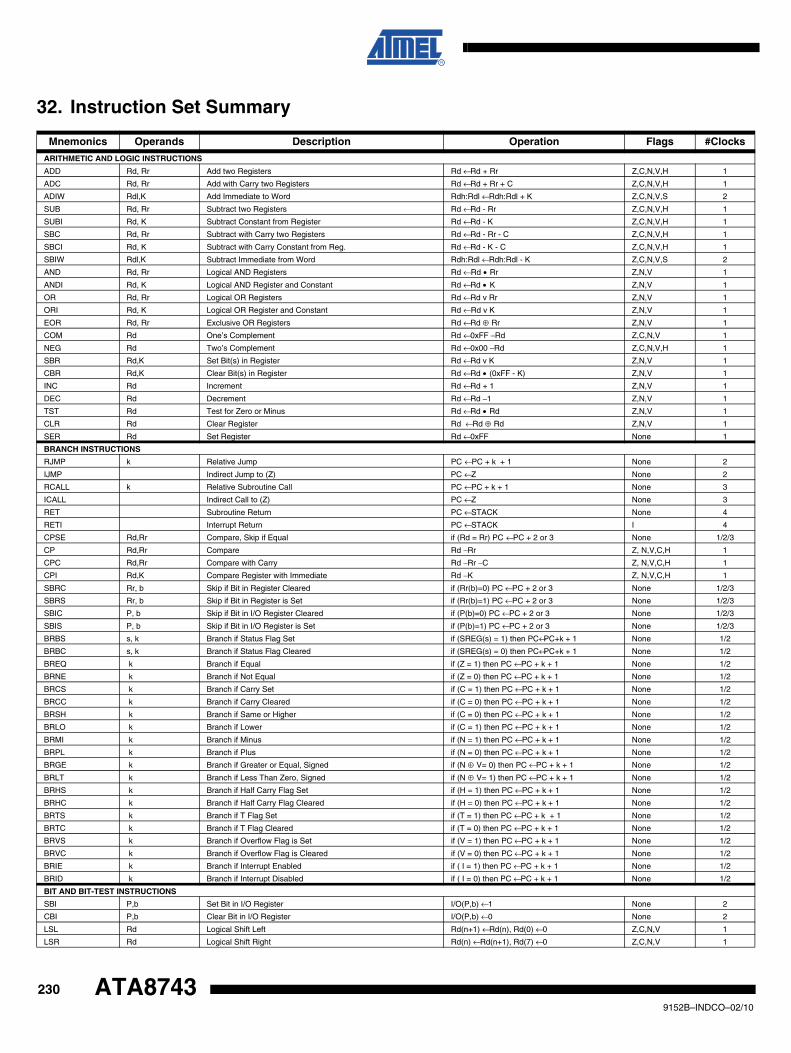
32. Instruction Set Summary
Mnemonics Operands Description Operation Flags #Clocks
ARITHMETIC AND LOGIC INSTRUCTIONS
ADD Rd, Rr Add two Registers Rd ← Rd + Rr Z,C,N,V,H 1
ADC Rd, Rr Add with Carry two Registers Rd ← Rd + Rr + C Z,C,N,V,H 1
ADIW Rdl,K Add Immediate to Word Rdh:Rdl ← Rdh:Rdl + K Z,C,N,V,S 2
SUB Rd, Rr Subtract two Registers Rd ← Rd - Rr Z,C,N,V,H 1
SUBI Rd, K Subtract Constant from Register Rd ← Rd - K Z,C,N,V,H 1
SBC Rd, Rr Subtract with Carry two Registers Rd ← Rd - Rr - C Z,C,N,V,H 1
SBCI Rd, K Subtract with Carry Constant from Reg. Rd ← Rd - K - C Z,C,N,V,H 1
SBIW Rdl,K Subtract Immediate from Word Rdh:Rdl ← Rdh:Rdl - K Z,C,N,V,S 2
AND Rd, Rr Logical AND Registers Rd ← Rd • Rr Z,N,V 1
ANDI Rd, K Logical AND Register and Constant Rd ← Rd • K Z,N,V 1
OR Rd, Rr Logical OR Registers Rd ← Rd v Rr Z,N,V 1
ORI Rd, K Logical OR Register and Constant Rd ← Rd v K Z,N,V 1
EOR Rd, Rr Exclusive OR Registers Rd ← Rd ⊕ Rr Z,N,V 1
COM Rd One’s Complement Rd ← 0xFF − Rd Z,C,N,V 1
NEG Rd Two’s Complement Rd ← 0x00 − Rd Z,C,N,V,H 1
SBR Rd,K Set Bit(s) in Register Rd ← Rd v K Z,N,V 1
CBR Rd,K Clear Bit(s) in Register Rd ← Rd • (0xFF - K) Z,N,V 1
INC Rd Increment Rd ← Rd + 1 Z,N,V 1
DEC Rd Decrement Rd ← Rd − 1 Z,N,V 1
TST Rd Test for Zero or Minus Rd ← Rd • Rd Z,N,V 1
CLR Rd Clear Register Rd ← Rd ⊕ Rd Z,N,V 1
SER Rd Set Register Rd ← 0xFF None 1
BRANCH INSTRUCTIONS
RJMP k Relative Jump PC ← PC + k + 1 None 2
IJMP Indirect Jump to (Z) PC ← Z None 2
RCALL k Relative Subroutine Call PC ← PC + k + 1 None 3
ICALL Indirect Call to (Z) PC ← Z None 3
RET Subroutine Return PC ← STACK None 4
RETI Interrupt Return PC ← STACK I 4
CPSE Rd,Rr Compare, Skip if Equal if (Rd = Rr) PC ← PC + 2 or 3 None 1/2/3
CP Rd,Rr Compare Rd − Rr Z, N,V,C,H 1
CPC Rd,Rr Compare with Carry Rd − Rr − C Z, N,V,C,H 1
CPI Rd,K Compare Register with Immediate Rd − K Z, N,V,C,H 1
SBRC Rr, b Skip if Bit in Register Cleared if (Rr(b)=0) PC ← PC + 2 or 3 None 1/2/3
SBRS Rr, b Skip if Bit in Register is Set if (Rr(b)=1) PC ← PC + 2 or 3 None 1/2/3
SBIC P, b Skip if Bit in I/O Register Cleared if (P(b)=0) PC ← PC + 2 or 3 None 1/2/3
SBIS P, b Skip if Bit in I/O Register is Set if (P(b)=1) PC ← PC + 2 or 3 None 1/2/3
BRBS s, k Branch if Status Flag Set if (SREG(s) = 1) then PC←PC+k + 1 None 1/2
BRBC s, k Branch if Status Flag Cleared if (SREG(s) = 0) then PC←PC+k + 1 None 1/2
BREQ k Branch if Equal if (Z = 1) then PC ← PC + k + 1 None 1/2
BRNE k Branch if Not Equal if (Z = 0) then PC ← PC + k + 1 None 1/2
BRCS k Branch if Carry Set if (C = 1) then PC ← PC + k + 1 None 1/2
BRCC k Branch if Carry Cleared if (C = 0) then PC ← PC + k + 1 None 1/2
BRSH k Branch if Same or Higher if (C = 0) then PC ← PC + k + 1 None 1/2
BRLO k Branch if Lower if (C = 1) then PC ← PC + k + 1 None 1/2
BRMI k Branch if Minus if (N = 1) then PC ← PC + k + 1 None 1/2
BRPL k Branch if Plus if (N = 0) then PC ← PC + k + 1 None 1/2
BRGE k Branch if Greater or Equal, Signed if (N ⊕ V= 0) then PC ← PC + k + 1 None 1/2
BRLT k Branch if Less Than Zero, Signed if (N ⊕ V= 1) then PC ← PC + k + 1 None 1/2
BRHS k Branch if Half Carry Flag Set if (H = 1) then PC ← PC + k + 1 None 1/2
BRHC k Branch if Half Carry Flag Cleared if (H = 0) then PC ← PC + k + 1 None 1/2
BRTS k Branch if T Flag Set if (T = 1) then PC ← PC + k + 1 None 1/2
BRTC k Branch if T Flag Cleared if (T = 0) then PC ← PC + k + 1 None 1/2
BRVS k Branch if Overflow Flag is Set if (V = 1) then PC ← PC + k + 1 None 1/2
BRVC k Branch if Overflow Flag is Cleared if (V = 0) then PC ← PC + k + 1 None 1/2
BRIE k Branch if Interrupt Enabled if ( I = 1) then PC ← PC + k + 1 None 1/2
BRID k Branch if Interrupt Disabled if ( I = 0) then PC ← PC + k + 1 None 1/2
BIT AND BIT-TEST INSTRUCTIONS
SBI P,b Set Bit in I/O Register I/O(P,b) ← 1 None 2
CBI P,b Clear Bit in I/O Register I/O(P,b) ← 0 None 2
LSL Rd Logical Shift Left Rd(n+1) ← Rd(n), Rd(0) ← 0 Z,C,N,V 1
LSR Rd Logical Shift Right Rd(n) ← Rd(n+1), Rd(7) ← 0 Z,C,N,V 1
2309152B–INDCO–02/10
ATA8743
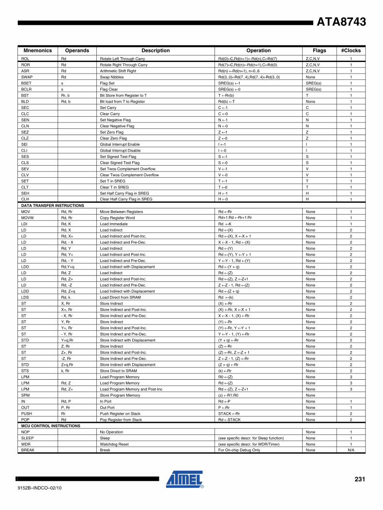
ATA8743
ROL Rd Rotate Left Through Carry Rd(0)←C,Rd(n+1)← Rd(n),C←Rd(7) Z,C,N,V 1
ROR Rd Rotate Right Through Carry Rd(7)←C,Rd(n)← Rd(n+1),C←Rd(0) Z,C,N,V 1
ASR Rd Arithmetic Shift Right Rd(n) ← Rd(n+1), n=0..6 Z,C,N,V 1
SWAP Rd Swap Nibbles Rd(3..0)←Rd(7..4),Rd(7..4)←Rd(3..0) None 1
BSET s Flag Set SREG(s) ← 1 SREG(s) 1
BCLR s Flag Clear SREG(s) ← 0 SREG(s) 1
BST Rr, b Bit Store from Register to T T ← Rr(b) T 1
BLD Rd, b Bit load from T to Register Rd(b) ← T None 1
SEC Set Carry C ← 1 C 1
CLC Clear Carry C ← 0 C 1
SEN Set Negative Flag N ← 1 N 1
CLN Clear Negative Flag N ← 0 N 1
SEZ Set Zero Flag Z ← 1 Z 1
CLZ Clear Zero Flag Z ← 0 Z 1
SEI Global Interrupt Enable I ← 1 I 1
CLI Global Interrupt Disable I ← 0 I 1
SES Set Signed Test Flag S ← 1 S 1
CLS Clear Signed Test Flag S ← 0 S 1
SEV Set Twos Complement Overflow. V ← 1 V 1
CLV Clear Twos Complement Overflow V ← 0 V 1
SET Set T in SREG T ← 1 T 1
CLT Clear T in SREG T ← 0 T 1
SEH Set Half Carry Flag in SREG H ← 1 H 1
CLH Clear Half Carry Flag in SREG H ← 0 H 1
DATA TRANSFER INSTRUCTIONS
MOV Rd, Rr Move Between Registers Rd ← Rr None 1
MOVW Rd, Rr Copy Register Word Rd+1:Rd ← Rr+1:Rr None 1
LDI Rd, K Load Immediate Rd ← K None 1
LD Rd, X Load Indirect Rd ← (X) None 2
LD Rd, X+ Load Indirect and Post-Inc. Rd ← (X), X ← X + 1 None 2
LD Rd, - X Load Indirect and Pre-Dec. X ← X - 1, Rd ← (X) None 2
LD Rd, Y Load Indirect Rd ← (Y) None 2
LD Rd, Y+ Load Indirect and Post-Inc. Rd ← (Y), Y ← Y + 1 None 2
LD Rd, - Y Load Indirect and Pre-Dec. Y ← Y - 1, Rd ← (Y) None 2
LDD Rd,Y+q Load Indirect with Displacement Rd ← (Y + q) None 2
LD Rd, Z Load Indirect Rd ← (Z) None 2
LD Rd, Z+ Load Indirect and Post-Inc. Rd ← (Z), Z ← Z+1 None 2
LD Rd, -Z Load Indirect and Pre-Dec. Z ← Z - 1, Rd ← (Z) None 2
LDD Rd, Z+q Load Indirect with Displacement Rd ← (Z + q) None 2
LDS Rd, k Load Direct from SRAM Rd ← (k) None 2
ST X, Rr Store Indirect (X) ← Rr None 2
ST X+, Rr Store Indirect and Post-Inc. (X) ← Rr, X ← X + 1 None 2
ST - X, Rr Store Indirect and Pre-Dec. X ← X - 1, (X) ← Rr None 2
ST Y, Rr Store Indirect (Y) ← Rr None 2
ST Y+, Rr Store Indirect and Post-Inc. (Y) ← Rr, Y ← Y + 1 None 2
ST - Y, Rr Store Indirect and Pre-Dec. Y ← Y - 1, (Y) ← Rr None 2
STD Y+q,Rr Store Indirect with Displacement (Y + q) ← Rr None 2
ST Z, Rr Store Indirect (Z) ← Rr None 2
ST Z+, Rr Store Indirect and Post-Inc. (Z) ← Rr, Z ← Z + 1 None 2
ST -Z, Rr Store Indirect and Pre-Dec. Z ← Z - 1, (Z) ← Rr None 2
STD Z+q,Rr Store Indirect with Displacement (Z + q) ← Rr None 2
STS k, Rr Store Direct to SRAM (k) ← Rr None 2
LPM Load Program Memory R0 ← (Z) None 3
LPM Rd, Z Load Program Memory Rd ← (Z) None 3
LPM Rd, Z+ Load Program Memory and Post-Inc Rd ← (Z), Z ← Z+1 None 3
SPM Store Program Memory (z) ← R1:R0 None
IN Rd, P In Port Rd ← P None 1
OUT P, Rr Out Port P ← Rr None 1
PUSH Rr Push Register on Stack STACK ← Rr None 2
POP Rd Pop Register from Stack Rd ← STACK None 2
MCU CONTROL INSTRUCTIONS
NOP No Operation None 1
SLEEP Sleep (see specific descr. for Sleep function) None 1
WDR Watchdog Reset (see specific descr. for WDR/Timer) None 1
BREAK Break For On-chip Debug Only None N/A
Mnemonics Operands Description Operation Flags #Clocks
2319152B–INDCO–02/10

Appendix 2: Appendix B - ATA8743/ATA8741/ATA8742 AutomotiveSpecification at 1.8V
2329152B–INDCO–02/10
ATA8743
ATA8743
33. DescriptionThis document contains information specific to devices operating at voltage between 1.8V and3.6V. Only deviations with standard operating characteristics are covered in this appendix, allother information can be found in the complete Automotive datasheet. The completeATtiny24/ATtiny44/ATtiny84 automotive datasheet can be found on www.atmel.com.
2339152B–INDCO–02/10
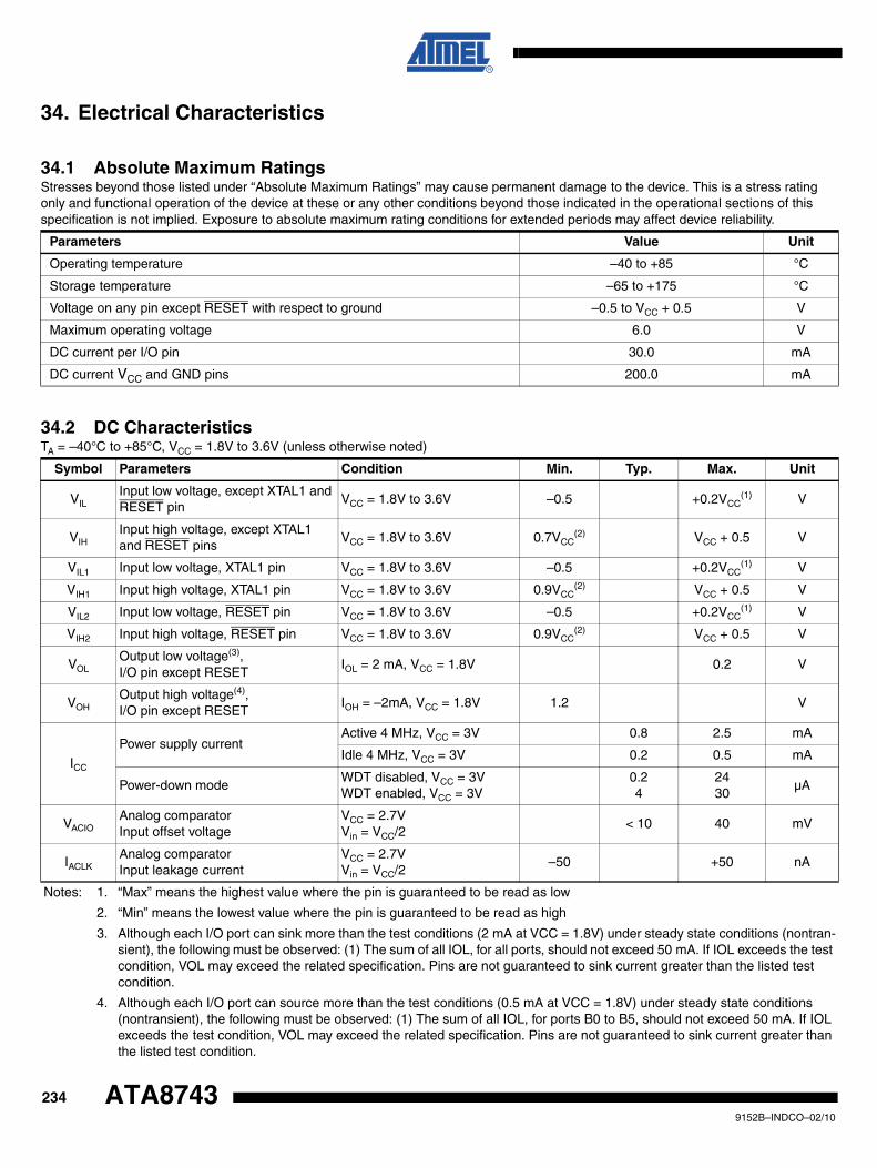
34. Electrical Characteristics
34.1 Absolute Maximum RatingsStresses beyond those listed under “Absolute Maximum Ratings” may cause permanent damage to the device. This is a stress rating only and functional operation of the device at these or any other conditions beyond those indicated in the operational sections of this specification is not implied. Exposure to absolute maximum rating conditions for extended periods may affect device reliability.
Parameters Value Unit
Operating temperature –40 to +85 °C
Storage temperature –65 to +175 °C
Voltage on any pin except RESET with respect to ground –0.5 to VCC + 0.5 V
Maximum operating voltage 6.0 V
DC current per I/O pin 30.0 mA
DC current VCC and GND pins 200.0 mA
34.2 DC CharacteristicsTA = –40°C to +85°C, VCC = 1.8V to 3.6V (unless otherwise noted)
Symbol Parameters Condition Min. Typ. Max. Unit
VILInput low voltage, except XTAL1 and RESET pin
VCC = 1.8V to 3.6V –0.5 +0.2VCC(1) V
VIHInput high voltage, except XTAL1 and RESET pins
VCC = 1.8V to 3.6V 0.7VCC(2) VCC + 0.5 V
VIL1 Input low voltage, XTAL1 pin VCC = 1.8V to 3.6V –0.5 +0.2VCC(1) V
VIH1 Input high voltage, XTAL1 pin VCC = 1.8V to 3.6V 0.9VCC(2) VCC + 0.5 V
VIL2 Input low voltage, RESET pin VCC = 1.8V to 3.6V –0.5 +0.2VCC(1) V
VIH2 Input high voltage, RESET pin VCC = 1.8V to 3.6V 0.9VCC(2) VCC + 0.5 V
VOLOutput low voltage(3), I/O pin except RESET
IOL = 2 mA, VCC = 1.8V 0.2 V
VOHOutput high voltage(4), I/O pin except RESET
IOH = –2mA, VCC = 1.8V 1.2 V
ICC
Power supply currentActive 4 MHz, VCC = 3V 0.8 2.5 mA
Idle 4 MHz, VCC = 3V 0.2 0.5 mA
Power-down modeWDT disabled, VCC = 3VWDT enabled, VCC = 3V
0.24
2430
µA
VACIOAnalog comparator Input offset voltage
VCC = 2.7VVin = VCC/2
< 10 40 mV
IACLKAnalog comparator Input leakage current
VCC = 2.7VVin = VCC/2
–50 +50 nA
Notes: 1. “Max” means the highest value where the pin is guaranteed to be read as low
2. “Min” means the lowest value where the pin is guaranteed to be read as high
3. Although each I/O port can sink more than the test conditions (2 mA at VCC = 1.8V) under steady state conditions (nontran-sient), the following must be observed: (1) The sum of all IOL, for all ports, should not exceed 50 mA. If IOL exceeds the test condition, VOL may exceed the related specification. Pins are not guaranteed to sink current greater than the listed test condition.
4. Although each I/O port can source more than the test conditions (0.5 mA at VCC = 1.8V) under steady state conditions (nontransient), the following must be observed: (1) The sum of all IOL, for ports B0 to B5, should not exceed 50 mA. If IOL exceeds the test condition, VOL may exceed the related specification. Pins are not guaranteed to sink current greater than the listed test condition.
2349152B–INDCO–02/10
ATA8743
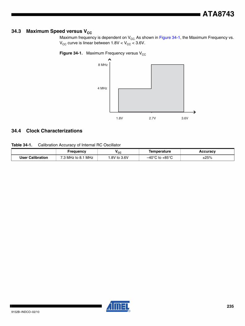
ATA8743
34.3 Maximum Speed versus VCCMaximum frequency is dependent on VCC. As shown in Figure 34-1, the Maximum Frequency vs.VCC curve is linear between 1.8V < VCC < 3.6V.
Figure 34-1. Maximum Frequency versus VCC
34.4 Clock Characterizations
4 MHz
8 MHz
1.8V 2.7V 3.6V
Safe Operating Area
Table 34-1. Calibration Accuracy of Internal RC Oscillator
Frequency VCC Temperature Accuracy
User Calibration 7.3 MHz to 8.1 MHz 1.8V to 3.6V –40°C to +85°C ±25%
2359152B–INDCO–02/10
34.5 ADC Characteristics TA = –40°C to +85°C, VCC = 1.8V to 3.6V (unless otherwise noted)
Symbol Parameters Test Conditions Min. Typ. Max. Unit
Resolution Single ended conversion 10 Bits
Absolute accuracy (Including INL, DNL, quantization error, gain and offset error)
VCC = 1.8V, VRef = 1.8V, ADC clock = 200 kHz
2 4.0 LSB
VCC = 1.8V, VRef = 1.8V, ADC clock = 200 kHzNoise Reduction Mode
2 4.0 LSB
Integral Non-Linearity (INL)VCC = 1.8V, VRef = 1.8V, ADC clock = 200 kHz
0.5 1.5 LSB
Differential Non-Linearity (DNL)VCC = 1.8V, VRef = 1.8V, ADC clock = 200 kHz
0.2 0.7 LSB
Gain errorVCC = 1.8V, VRef = 1.8V, ADC clock = 200 kHz
–7.0 –3.0 +5.0 LSB
Offset errorVCC = 1.8V, VRef = 1.8V, ADC clock = 200 kHz
–3.5 +1.5 +3.5 LSB
VREF Reference voltage 1.8 AVCC V
34.6 ADC Characteristics TA = –40°C to +85°C, VCC = 1.8V to 3.6V (unless otherwise noted)
Symbol Parameters Test Conditions Min. Typ. Max. Unit
ResolutionDifferential conversion, gain = 1xBIPOLAR mode only
8 Bits
Absolute accuracy (Including INL, DNL, quantization error, gain and offset error)
Gain = 1x, VCC = 1.8V, VRef = 1.3V, ADC clock = 125 kHz
1.6 5.0 LSB
Integral Non-Linearity (INL)Gain = 1x, VCC = 1.8V, VRef = 1.3V,ADC clock = 125kHz
0.7 2.5 LSB
Differential Non-Linearity (DNL)Gain = 1x, VCC = 1.8V,VRef = 1.3V,ADC clock = 125 kHz
0.3 1.0 LSB
Gain ErrorGain = 1x, VCC = 1.8V,VRef = 1.3V, ADC clock = 125 kHz
–7.0 +1.50 +7.0 LSB
Offset ErrorGain = 1x, VCC = 1.8V.VRef = 1.3V,ADC clock = 125 kHz
–4.0 0.0 +4.0 LSB
VREF Reference Voltage 1.30AVCC –
0.5V
2369152B–INDCO–02/10
ATA8743
ATA8743
36. Package Information
37. Revision History
35. Ordering InformationExtended Type Number Package Remarks
ATA8743-PXQW QFN24 5 mm x 5 mm Microcontroller with UHF Tx for 868 MHz to 928 MHz
specificationsaccording to DINtechnical drawings
0.3
0.4
0.9±0.1
Not indicated tolerances ±0.05
0.65 nom.
0.05-0.05+0
12 7
19 24
13
18
6
24
1
6
1
Issue: 1; 15.11.05
Drawing-No.: 6.543-5122.01-4
5
3.25
3.6
Dimensions in mm
Package: QFN 24 - 5 x 5 Exposed pad 3.6 x 3.6(acc. JEDEC OUTLINE No. MO-220)
Please note that the following page numbers referred to in this section refer to the specific revision mentioned, not to this document.
Revision No. History
9152B-INDCO-02/10• Section 7 “Electrical Characteristics” on page 10 changed
• Section 35 “Ordering Information” on page 237 changed
2379152B–INDCO–02/10
9152B–INDCO–02/10
Headquarters International
Atmel Corporation2325 Orchard ParkwaySan Jose, CA 95131USATel: 1(408) 441-0311Fax: 1(408) 487-2600
Atmel AsiaUnit 1-5 & 16, 19/FBEA Tower, Millennium City 5418 Kwun Tong RoadKwun Tong, KowloonHong KongTel: (852) 2245-6100Fax: (852) 2722-1369
Atmel EuropeLe Krebs8, Rue Jean-Pierre TimbaudBP 30978054 Saint-Quentin-en-Yvelines CedexFranceTel: (33) 1-30-60-70-00 Fax: (33) 1-30-60-71-11
Atmel Japan9F, Tonetsu Shinkawa Bldg.1-24-8 ShinkawaChuo-ku, Tokyo 104-0033JapanTel: (81) 3-3523-3551Fax: (81) 3-3523-7581
Product Contact
Web Sitewww.atmel.com
Technical [email protected]
Sales Contactwww.atmel.com/contacts
Literature Requestswww.atmel.com/literature
Disclaimer: The information in this document is provided in connection with Atmel products. No license, express or implied, by estoppel or otherwise, to anyintellectual property right is granted by this document or in connection with the sale of Atmel products. EXCEPT AS SET FORTH IN ATMEL’S TERMS AND CONDI-TIONS OF SALE LOCATED ON ATMEL’S WEB SITE, ATMEL ASSUMES NO LIABILITY WHATSOEVER AND DISCLAIMS ANY EXPRESS, IMPLIED OR STATUTORYWARRANTY RELATING TO ITS PRODUCTS INCLUDING, BUT NOT LIMITED TO, THE IMPLIED WARRANTY OF MERCHANTABILITY, FITNESS FOR A PARTICULARPURPOSE, OR NON-INFRINGEMENT. IN NO EVENT SHALL ATMEL BE LIABLE FOR ANY DIRECT, INDIRECT, CONSEQUENTIAL, PUNITIVE, SPECIAL OR INCIDEN-TAL DAMAGES (INCLUDING, WITHOUT LIMITATION, DAMAGES FOR LOSS OF PROFITS, BUSINESS INTERRUPTION, OR LOSS OF INFORMATION) ARISING OUT OFTHE USE OR INABILITY TO USE THIS DOCUMENT, EVEN IF ATMEL HAS BEEN ADVISED OF THE POSSIBILITY OF SUCH DAMAGES. Atmel makes norepresentations or warranties with respect to the accuracy or completeness of the contents of this document and reserves the right to make changes to specificationsand product descriptions at any time without notice. Atmel does not make any commitment to update the information contained herein. Unless specifically providedotherwise, Atmel products are not suitable for, and shall not be used in, automotive applications. Atmel’s products are not intended, authorized, or warranted for useas components in applications intended to support or sustain life.
© 2010 Atmel Corporation. All rights reserved. Atmel®, Atmel logo and combinations thereof, AVR®, AVR Studio® and others are registeredtrademarks or trademarks of Atmel Corporation or its subsidiaries. Other terms and product names may be trademarks of others.
![MERCEDES CLK, MERCEDES-BENZ CLK, DAIMLERCHRYSLER CLK · 23037 • 1.0 • 18/07/2014 2 23037 mercedes clk, mercedes-benz clk, daimlerchrysler clk coupÉ (no cabrio) [2002+] type 209](https://img.pdfslide.us/doc/110x75/60c1598cbaa5c6282b3f3f58/mercedes-clk-mercedes-benz-clk-daimlerchrysler-clk-23037-a-10-a-18072014.jpg)