Embed Size (px)
Citation preview
Microcontroller System ArchitectureEach MCU (micro-controller unit) is
characterized by:• Microprocessor
• 8,16,32 bit architecture• Usually “simple” in-order
microarchitecture, no FPU
Example: STM32F101 MCU

Microcontroller System ArchitectureEach MCU (micro-controller unit) is
characterized by:• Microprocessor
• 8,16,32 bit architecture• Usually “simple” in-order
microarchitecture, no FPU• Memory
• RAM (from 512B to 256kB)• FLASH (from 512B to 1MB)
Example: STM32F101 MCU

Microcontroller System ArchitectureEach MCU (micro-controller unit) is
characterized by:• Microprocessor
• 8,16,32 bit architecture• Usually “simple” in-order
microarchitecture, no FPU• Memory
• RAM (from 512B to 256kB)• FLASH (from 512B to 1MB)
• Peripherals• DMA• Timer• Interfaces
• Digital• Analog
Example: STM32F101 MCUDMAs
InterfacesTimer

Microcontroller System ArchitectureEach MCU (micro-controller unit) is
characterized by:• Microprocessor
• 8,16,32 bit architecture• Usually “simple” in-order
microarchitecture, no FPU• Memory
• RAM (from 512B to 256kB)• FLASH (from 512B to 1MB)
• Peripherals• DMA• Timer• Interfaces
• Digital• Analog
• Interconnect• AHB system bus (ARM-based MCUs)• APB peripheral bus (ARM-based MCUs)
Example: STM32F101 MCU

Microcontroller System ArchitectureEach MCU (micro-controller unit) is
characterized by:• Microprocessor
• 8,16,32 bit architecture• Usually “simple” in-order
microarchitecture, no FPU• Memory
• RAM (from 512B to 256kB)• FLASH (from 512B to 1MB)
• Peripherals• DMA• Timer• Interfaces
• Digital• Analog
• Interconnect• AHB system bus (ARM-based MCUs)• APB peripheral bus (ARM-based MCUs)
Example: STM32F101 MCU
MCU Interfaces• Digital
• Several protocols for inter-chip communication
UART, I2C, SPI, USB,…• Serial communication protocols
• Meant for short distances “inside the box” / on-board• Low complexity• Low cost• Low speed ( a few Mb/s at the fastest )• Serial communication is employed where it is not practical, either in physical or
cost terms, to move data in parallel between systems.
• Analog• ADC (Analog-to-Digital Converter)• DAC (Digital-to-Analog Converter)• Comparator

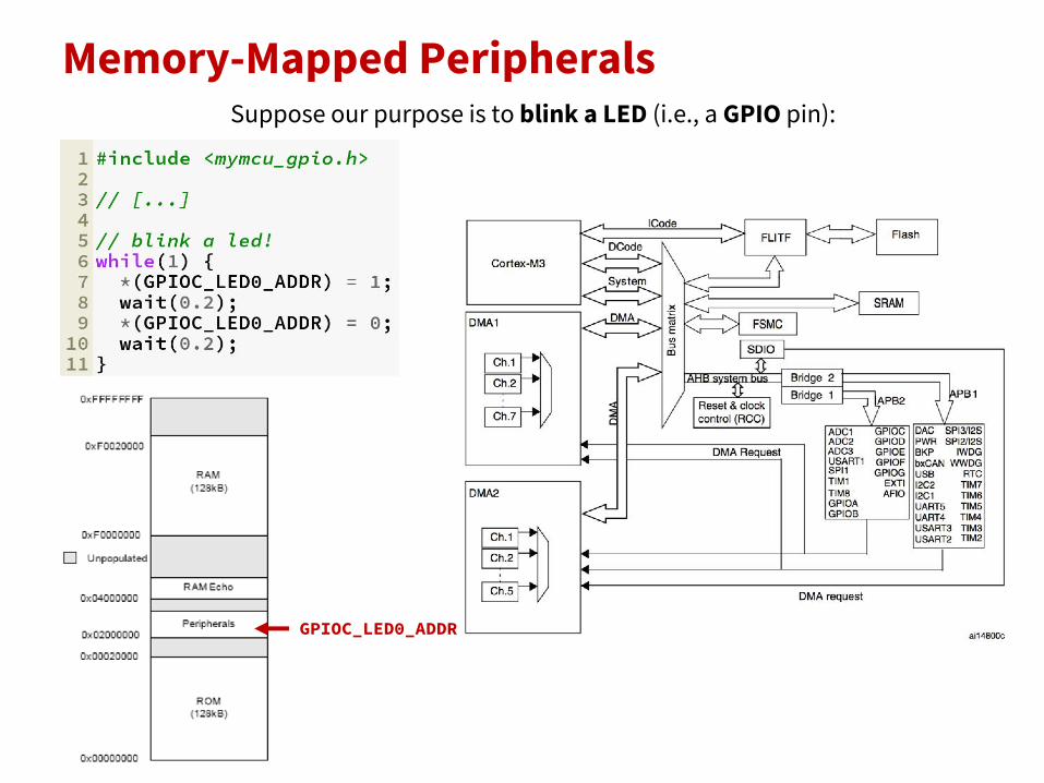
Memory-Mapped PeripheralsPeripherals such as external interfaces in a microcontroller system are accessible via memory-mapped registers:
• for peripheral configuration• for I/O
Cortex-M3MCU core
memory mappedload/store
addresses Memory Map

GPIOC_LED0_ADDR
Suppose our purpose is to blink a LED (i.e., a GPIO pin):
Memory-Mapped Peripherals
GPIOC_LED0_ADDR
Suppose our purpose is to blink a LED (i.e., a GPIO pin):
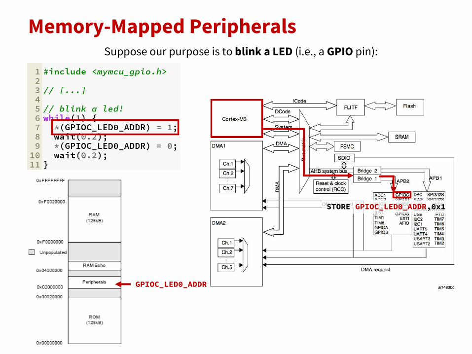
Memory-Mapped Peripherals

GPIOC_LED0_ADDR
STORE GPIOC_LED0_ADDR,0x1
Suppose our purpose is to blink a LED (i.e., a GPIO pin):
Memory-Mapped Peripherals

GPIOC_LED0_ADDR
STORE GPIOC_LED0_ADDR,0x1
Suppose our purpose is to blink a LED (i.e., a GPIO pin):
Memory-Mapped Peripherals
GPIOC_LED0_ADDR
Suppose our purpose is to blink a LED (i.e., a GPIO pin):
Memory-Mapped Peripherals
STORE GPIOC_LED0_ADDR,0x1
MCUs are often pin-limited• Not enough I/O pins for all I/O peripherals and functions!
Microcontroller External Pins Configuration

MCUs are often pin-limited• Not enough I/O pins for all I/O peripherals and functions!• Pins have to be multiplexed (shared) between peripherals and functions
Microcontroller External Pins Configuration

MCUs are often pin-limited• Not enough I/O pins for all I/O peripherals and functions!• Pins have to be multiplexed (shared) between peripherals and functions
Most pins can be configured for several functions:• As input or output pin• As an interrupt pin• Setup a pull-up / pull-down internal resistor (NO floating pins!)
Microcontroller External Pins Configuration

MCUs are often pin-limited• Not enough I/O pins for all I/O peripherals and functions!• Pins have to be multiplexed (shared) between peripherals and functions
Most pins can be configured for several functions:• As input or output pin• As an interrupt pin• Setup a pull-up / pull-down internal resistor (NO floating pins!)• Assigned as general-purpose I/O (GPIO) or to a specific peripheral
• Digital peripherals such as UARTs, SPIs, I2Cs• Analog peripherals such as ADCs or DACs
Microcontroller External Pins Configuration
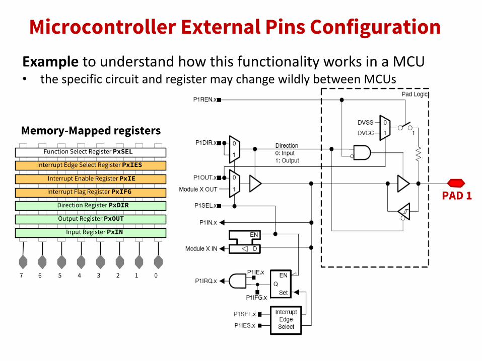
Microcontroller External Pins ConfigurationExample to understand how this functionality works in a MCU• the specific circuit and register may change wildly between MCUs
01234567
Input Register PxIN
Output Register PxOUT
Direction Register PxDIR
Interrupt Flag Register PxIFG
Interrupt Enable Register PxIE
Interrupt Edge Select Register PxIES
Function Select Register PxSEL
PAD 1
Memory-Mapped registers

Serial Interface Standards
https://xkcd.com/927/

I2C: Inter-Integrated Circuit Bus - 1• Usually pronounced “I-Squared-C”• Introduced by Philips (now NXP Semiconductors) in 1982

I2C: Inter-Integrated Circuit Bus - 1• Usually pronounced “I-Squared-C”• Introduced by Philips (now NXP Semiconductors) in 1982 • Used for communication with external peripherals, for
example:• EEPROMs• thermal sensors• real-time clocks

I2C: Inter-Integrated Circuit Bus - 1• Usually pronounced “I-Squared-C”• Introduced by Philips (now NXP Semiconductors) in 1982 • Used for communication with external peripherals, for
example:• EEPROMs• thermal sensors• real-time clocks
• Also used as a control interface for signal processing devices with separate data interfaces, for example:• radio frequency tuners• video decoders and encoders• audio processors

I2C: Inter-Integrated Circuit Bus - 2• Three supported speed modes:
• slow (under 100 Kbps)• fast (400 Kbps)• high-speed (3.4 Mbps) – in I2C v.2.0
• Maximum inter-IC distance of about 3 meters• (for moderate speeds, less for high-speed)

I2C: Inter-Integrated Circuit Bus - 2• Three supported speed modes:
• slow (under 100 Kbps)• fast (400 Kbps)• high-speed (3.4 Mbps) – in I2C v.2.0
• Maximum inter-IC distance of about 3 meters• (for moderate speeds, less for high-speed)
• Can support multi-master mode• For complex applications• Communication is always started by a master, both in single-master
and multi-master mode
• Half-duplex synchronous communication scheme• the master of the communication generates the clock (SCL) on which
data (SDA) is synchronized
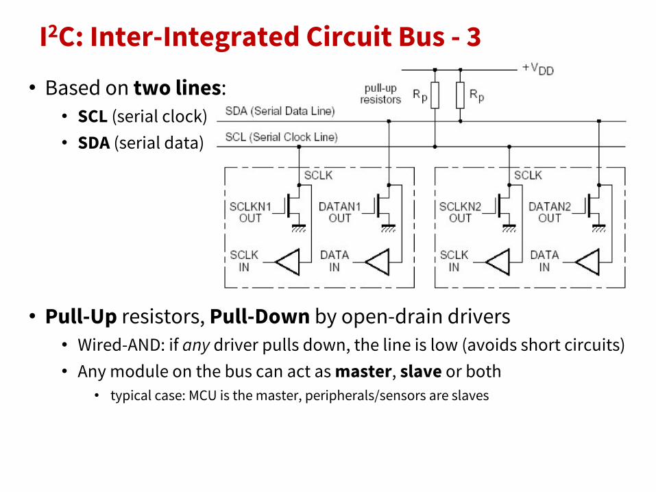
I2C: Inter-Integrated Circuit Bus - 3• Based on two lines:
• SCL (serial clock)• SDA (serial data)
• Pull-Up resistors, Pull-Down by open-drain drivers• Wired-AND: if any driver pulls down, the line is low (avoids short circuits)• Any module on the bus can act as master, slave or both
• typical case: MCU is the master, peripherals/sensors are slaves

I2C: Interface Protocol
SCL
SDA
start bit
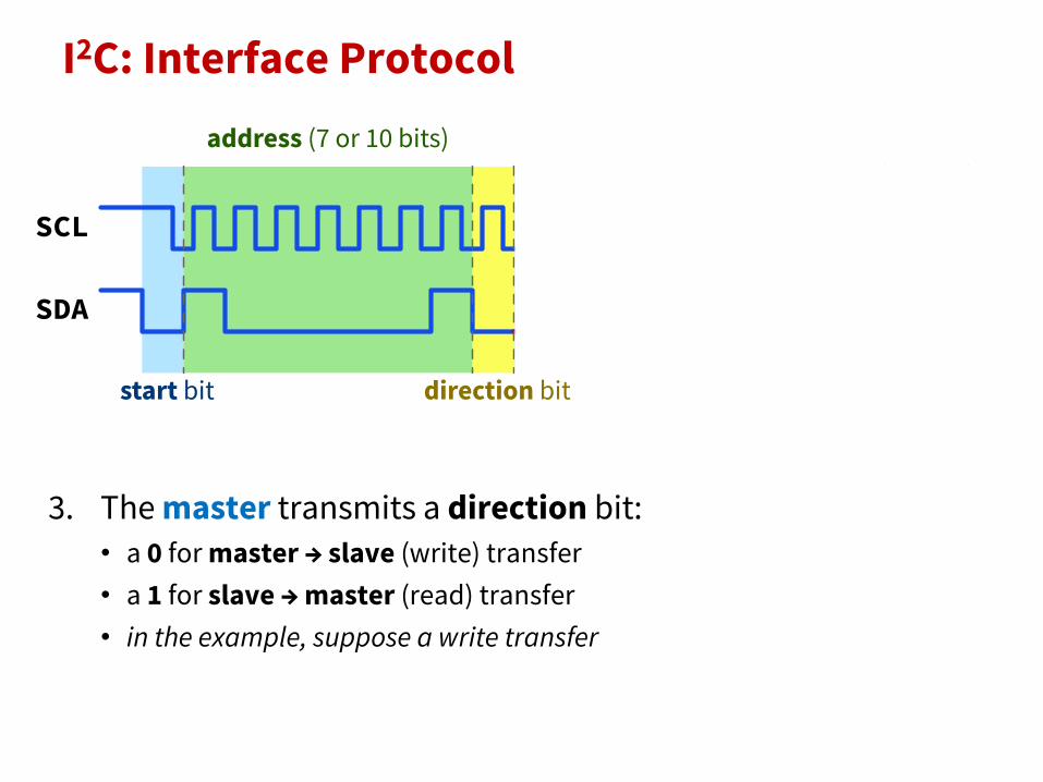
address (7 or 10 bits)
direction bit
ack bit
data payload
ack bit
stop bit
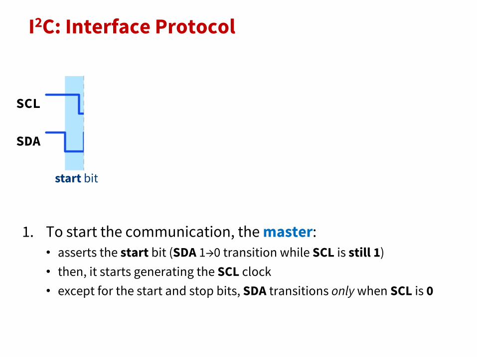
• In idle, both SCL and SDA are pulled-up to 1
I2C: Interface Protocol
SCL
SDA
start bit
address (7 or 10 bits)
direction bit
ack bit
data payload
ack bit
stop bit
1. To start the communication, the master:• asserts the start bit (SDA 1→0 transition while SCL is still 1)• then, it starts generating the SCL clock• except for the start and stop bits, SDA transitions only when SCL is 0

I2C: Interface Protocol
SCL
SDA
start bit
address (7 or 10 bits)
direction bit
ack bit
data payload
ack bit
stop bit
2. The master transmits the slave address:• broadcasted to all devices on the I2C bus• used to select the target slave• either 7 bits or 10 bits (newer devices – 7 bits address space is small!)• in the example, the address is 7’b1000001
I2C: Interface Protocol
SCL
SDA
start bit
address (7 or 10 bits)
direction bit
ack bit
data payload
ack bit
stop bit
3. The master transmits a direction bit:• a 0 for master → slave (write) transfer• a 1 for slave → master (read) transfer• in the example, suppose a write transfer

I2C: Interface Protocol
SCL
SDA
start bit
address (7 or 10 bits)
direction bit
ack bit
data payload
ack bit
stop bit
4. The slave then acknowledges reception:• by driving SDA to 0• if not acknowledged, the transaction must be repeated by the master

I2C: Interface Protocol
SCL
SDA
start bit
address (7 or 10 bits)
direction bit
ack bit
data payload
ack bit
stop bit
5. The master transmits its data payload:• each payload packet is 8 bits• there might be more than one packet, depending on application• in the example, data payload is 8’b00110100

I2C: Interface Protocol
SCL
SDA
start bit
address (7 or 10 bits)
direction bit
ack bit
data payload
ack bit
stop bit
6. The slave acknowledges reception of the data packet:• 1 ack bit every 8 payload bits• slave must acknowledge each packet

I2C: Interface Protocol
SCL
SDA
start bit
address (7 or 10 bits)
direction bit
ack bit
data payload
ack bit
stop bit
7. At the end of the transfer, the master transmits a stop bit:• first, it sets SDA to 0• then it releases SCL (i.e. it lets it go to 1)• finally, it releases SDA which also goes to 1

I2C: Interface Protocol
SCL
SDA
start bit
address (7 or 10 bits)
direction bit
ack bit
data payload
ack bit
stop bit
Reads work similarly, but data transfer – ack roles are reversed: • the slave drives SDA when transmitting the data byte• the master acknowledges the transfer

I2C: Clock Stretching
Slave can ask for more time to process a bit by clock stretching: • drive SCL to 0 if in need of more processing time
SCL
SDA

I2C: MCU-Sensor Communication ExampleExample of MCU – sensor communication (data acquisition) via I2C bus
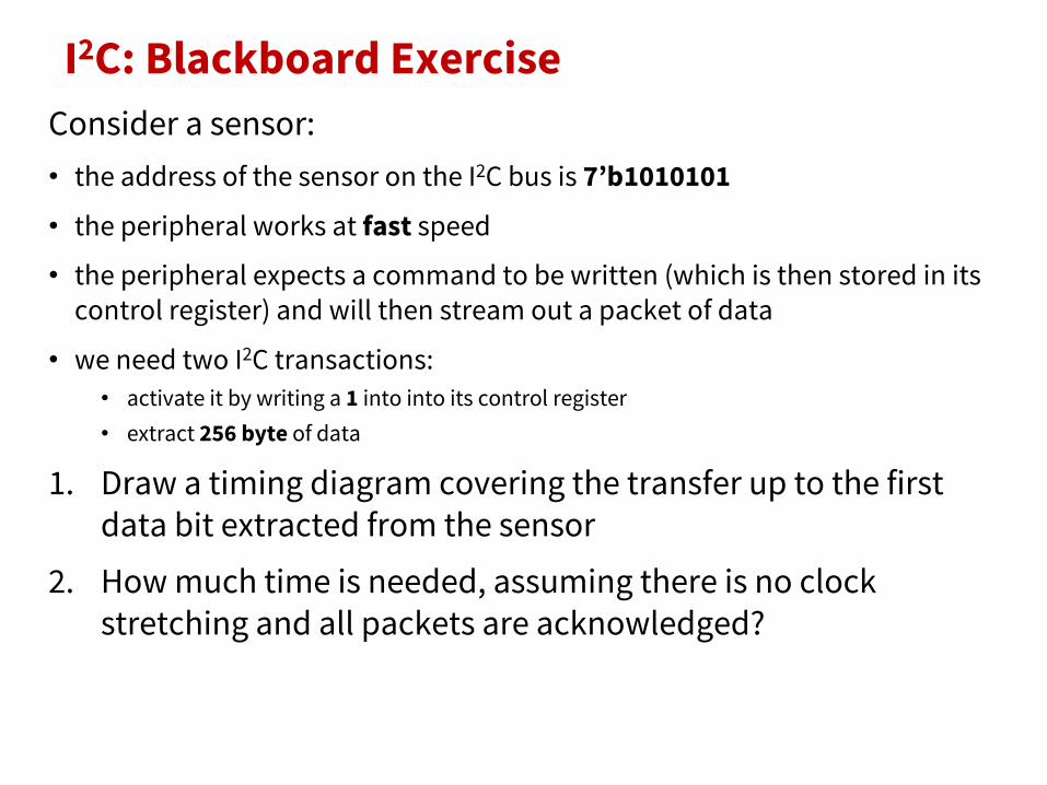
I2C: Blackboard ExerciseConsider a sensor:• the address of the sensor on the I2C bus is 7’b1010101• the peripheral works at fast speed
• the peripheral expects a command to be written (which is then stored in its control register) and will then stream out a packet of data
• we need two I2C transactions:• activate it by writing a 1 into into its control register• extract 256 byte of data
1. Draw a timing diagram covering the transfer up to the first data bit extracted from the sensor
2. How much time is needed, assuming there is no clock stretching and all packets are acknowledged?

SPI: Serial Peripheral Interface - 1
• Introduced by Motorola (now Freescale Semiconductors) for the MC68HCxx line of microcontrollers• Use cases are generally similar to I2C• Generally faster than I2C (up to several Mbit/s)
• Short-distance (i.e. on printed circuit boards)

SPI: Serial Peripheral Interface - 1
• Introduced by Motorola (now Freescale Semiconductors) for the MC68HCxx line of microcontrollers• Use cases are generally similar to I2C• Generally faster than I2C (up to several Mbit/s)
• Short-distance (i.e. on printed circuit boards)
• Single-master, multiple slave• needs one chip select per slave device (no broadcast addressing)
• Full-duplex synchronous communication scheme• master drives the clock (SCLK or SCK)
• clock polarity (i.e. write/read edges) and phase depend on specific application!

SPI: Serial Peripheral Interface - 2
• Based on two data and two control lines:• MISO (master-in, slave-out data)• MOSI (master-out, slave-in data)• SCK (clock)• CSN (chip select, one per slave – usually active low)
• Names are not standard, beware! Some possible alternatives:• SDI (SPI data in) instead of MISO• SDO (SPI data out) instead of MOSI• SCLK, CLK, SPC, … instead of SCK• CS, SS (slave select), SSN (slave select, active low) ... instead of CSN
MCU device
MOSIMISO
CLKCSN

SPI: Serial Peripheral Interface - 3• Full-duplex transfer: data is streamed between master and
slave shift-registers / FIFO buffers:• the master pushes the content of its buffer to the slave via MOSI• the slave pushes the content of its buffer to the master via MISO
• Processing / sensing / … happens in between (dashed line)
MOSI
MISO
FIFO in
FIFO out
FIFO out
FIFO in
MCU device

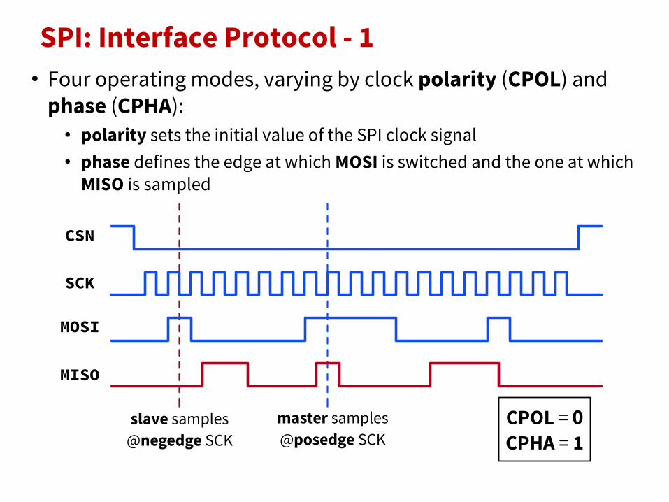
SPI: Interface Protocol - 1• Four operating modes, varying by clock polarity (CPOL) and
phase (CPHA):• polarity sets the initial value of the SPI clock signal• phase defines the edge at which MOSI is switched and the one at which
MISO is sampled
SCK
MOSI
CSN
MISO
slave samples@posedge SCK
master samples@negedge SCK
CPOL = 0CPHA = 0
SPI: Interface Protocol - 1• Four operating modes, varying by clock polarity (CPOL) and
phase (CPHA):• polarity sets the initial value of the SPI clock signal• phase defines the edge at which MOSI is switched and the one at which
MISO is sampled
SCK
MOSI
CSN
MISO
slave samples@negedge SCK
master samples@posedge SCK
CPOL = 1CPHA = 1
0

SPI: Interface Protocol -1• Four operating modes, varying by clock polarity (CPOL) and
phase (CPHA):• polarity sets the initial value of the SPI clock signal• phase defines the edge at which MOSI is switched and the one at which
MISO is sampled
SCK
MOSI
CSN
MISO
slave samples@negedge SCK
master samples@posedge SCK
CPOL = 1CPHA = 0

SPI: Interface Protocol -1• Four operating modes, varying by clock polarity (CPOL) and
phase (CPHA):• polarity sets the initial value of the SPI clock signal• phase defines the edge at which MOSI is switched and the one at which
MISO is sampled
SCK
MOSI
CSN
MISO
slave samples@posedge SCK
master samples@negedge SCK
CPOL = 1CPHA = 1

SPI: Interface Protocol - 2• Master completely in charge of transfer
• no ack, no clock stretching contrarily to I2C

SPI: Interface Protocol - 2• Master completely in charge of transfer
• no ack, no clock stretching contrarily to I2C
• More complex behavior than simple data streaming can be mapped on top of SPI protocol• e.g. command + address + data streaming

SPI vs I2C• For point-to-point, SPI is simple
and efficient• Less overhead than I2C due to lack of
addressing, plus SPI is full-duplex.
• For multiple slaves, each slave needs separate slave select signal• SPI requires more effort and more
hardware than I2C
• Quad-SPI also exists• 4x the bandwidth, often used by
Flash drives
SPI
I2C
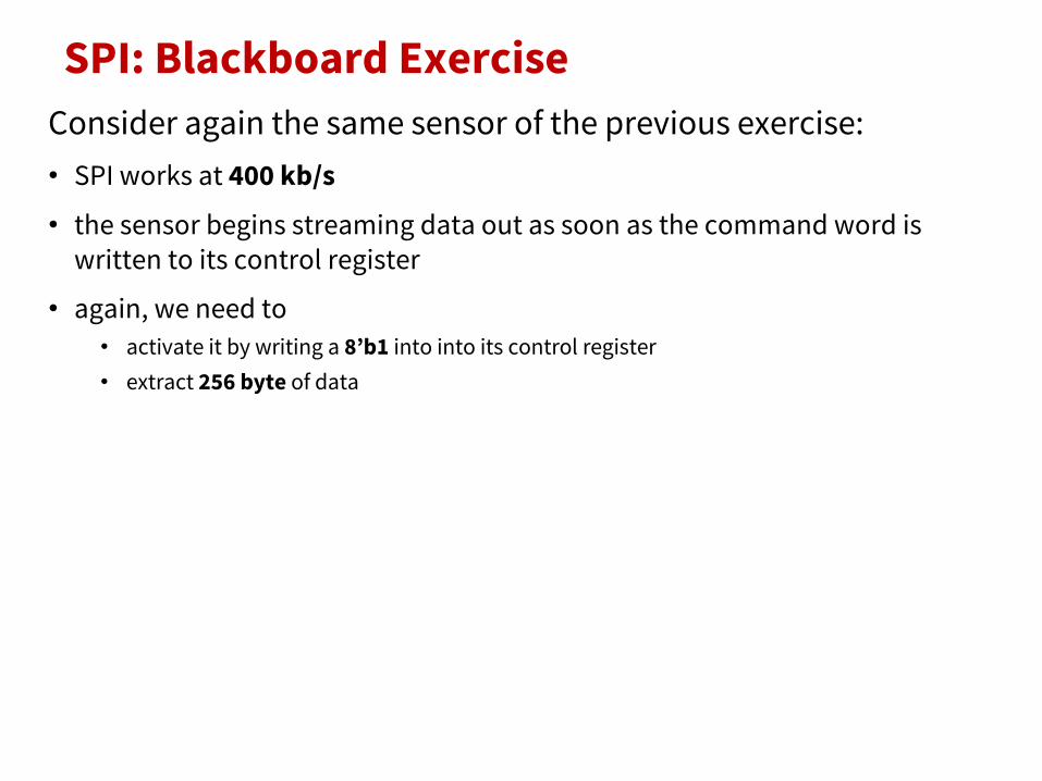
SPI: Blackboard ExerciseConsider again the same sensor of the previous exercise:• SPI works at 400 kb/s• the sensor begins streaming data out as soon as the command word is
written to its control register
• again, we need to• activate it by writing a 8’b1 into into its control register• extract 256 byte of data
1. How much time is needed for the transfer?

SPI: Blackboard ExerciseConsider again the same sensor of the previous exercise:• SPI works at 400 kb/s• the sensor begins streaming data out as soon as the command word is
written to its control register
• again, we need to• activate it by writing a 8’b1 into into its control register• extract 256 byte of data
1. How much time is needed for the transfer?2. How much time would be needed if the transfer speed was
1.2 Mb/s?

SPI: Blackboard ExerciseConsider again the same sensor of the previous exercise:• SPI works at 400 kb/s• the sensor begins streaming data out as soon as the command word is
written to its control register
• again, we need to• activate it by writing a 8’b1 into into its control register• extract 256 byte of data
1. How much time is needed for the transfer?2. How much time would be needed if the transfer speed was
1.2 Mb/s?3. What if the transfer involves 1) writing a 8 bit control register
2) writing 256 byte of data, 3) reading 256 byte of data?• Assume that to begin producing its output, the peripheral needs only
the first 2 bytes of the input

UART - 1
• Stands for Universal Asynchronous Receiver-Transmitter• sometimes also found as USART (Universal Synchronous-
Asynchronous Receiver Transmitter)
UART - 1
• Stands for Universal Asynchronous Receiver-Transmitter• sometimes also found as USART (Universal Synchronous-
Asynchronous Receiver Transmitter)
• Used to interface MCUs with other computing devices:• Communication with other processors, a PC (e.g. a serial terminal)• Used to interface the microcontroller with others transmission bus as:
RS232, RS485, USB, CAN BUS, KNX, LonWorks ecc.• Used to connect MCUs with modems and transceivers as telephone
modems, Bluetooth, Wi-Fi, GSM/GPRS/HDPSA

UART - 2• Essentially a parallel2serial (TX), serial2parallel (RX)
converter couple• e.g. using shift registers for P2S conversion

UART - 2• Essentially a parallel2serial (TX), serial2parallel (RX)
converter couple• e.g. using shift registers for P2S conversion
• Asynchronous: no common clock shared• Each device has its own local clock, typically running faster than the bit
rate (e.g. 8x faster)• The phase of the receiver clock is locked onto the edge of the
transmitted data
MCU deviceTX
RX
RX
TX

UART - 2• Essentially a parallel2serial (TX), serial2parallel (RX)
converter couple• e.g. using shift registers for P2S conversion
• Asynchronous: no common clock shared• Each device has its own local clock, typically running faster than the bit
rate (e.g. 8x faster)• The phase of the receiver clock is locked onto the edge of the
transmitted data
• Highly configurable• parity / no parity• data framing (e.g number of stop bits, number of payload bits)• simplex, full-duplex or half-duplex
MCU deviceTX
RX
RX
TX
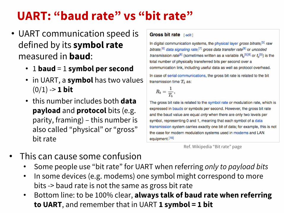
UART: “baud rate” vs “bit rate”• UART communication speed is
defined by its symbol rate measured in baud:• 1 baud = 1 symbol per second• in UART, a symbol has two values
(0/1) -> 1 bit• this number includes both data
payload and protocol bits (e.g. parity, framing) – this number is also called “physical” or “gross” bit rate
• This can cause some confusion• Some people use “bit rate” for UART when referring only to payload bits• In some devices (e.g. modems) one symbol might correspond to more
bits -> baud rate is not the same as gross bit rate• Bottom line: to be 100% clear, always talk of baud rate when referring
to UART, and remember that in UART 1 symbol = 1 bit
Ref. Wikipedia “Bit rate” page
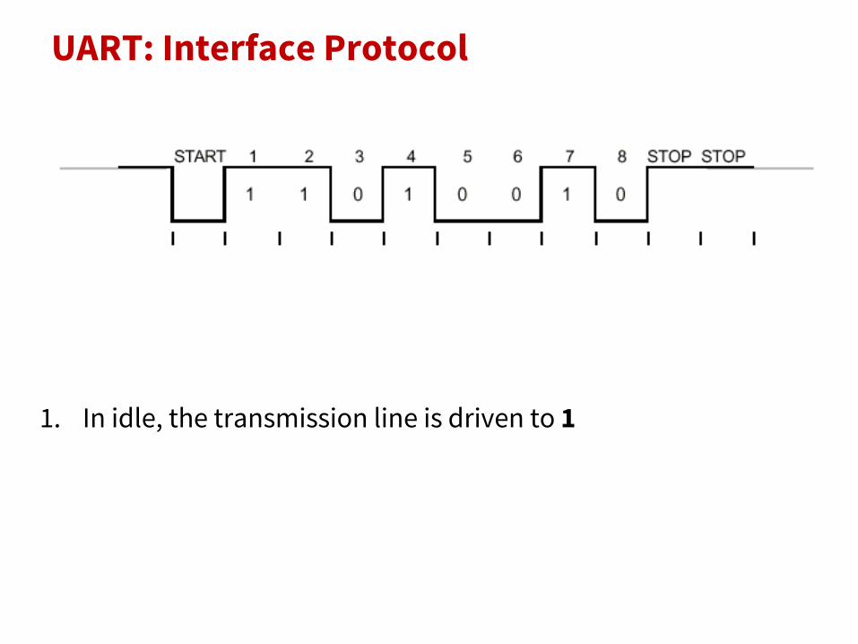
UART: Interface Protocol
1. In idle, the transmission line is driven to 1

UART: Interface Protocol
1 start bit
2. The transfer begins with a start bit:• the transmission line is driven to 0

UART: Interface Protocol
1 start bit 5-9 data bits
2. Then, a symbol of 5 to 9 bits is transmitted:• most often, 8 bits (1 ASCII character)• the symbol size is defined by the application and known a-priori with
respect to the communication

UART: Interface Protocol
1 start bit 4-8 data bits 1 parity bit
3. One of the data bits can be used for parity:
• odd parity even parity
• in this case, 4-8 bits can be used for data
peven =N
XNORi=1
bipodd =N
XORi=1
bi

UART: Interface Protocol
1 start bit 4-8 data bits 1 parity bit 1-2 stop bits
4. Finally, 1-2 stop bits:• Transmission line brought back to 1• 1 or 2 stop bits depending on application

UART: HandshakeThe UART protocol can also include a handshake:• request-to-send (RTS) signal from the MCU to the device means that the
MCU can accept new data
• clear-to-send (CTS) signal from the device to the MCU means that the device can send new data
• signals have dual meaning if seen from the other point of view
• exchange happens when CTS and RTS are both asserted
MCU device
TXRX
CTSRTS
RTSCTS
RXTX

UART: blackboard exerciseConsider an MCU connected to a PC via UART (e.g. over USB)• assume a baud rate of 9600 baud• the MCU uses parity, 1 start bit and 1 stop bit and transmits a payload of 8
bits per frame
• assume the MCU needs to print 1024 ASCII characters via the UART serial terminal to the PC
1. How much time is needed for the transfer?2. How much time with a baud rate of 115200 baud?
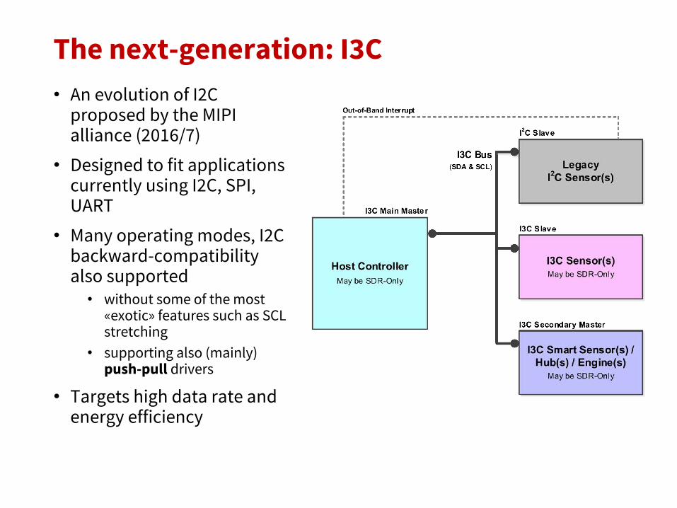
The next-generation: I3C• An evolution of I2C
proposed by the MIPI alliance (2016/7)
• Designed to fit applicationscurrently using I2C, SPI, UART
• Many operating modes, I2C backward-compatibilityalso supported• without some of the most
«exotic» features such as SCL stretching
• supporting also (mainly) push-pull drivers
• Targets high data rate and energy efficiency
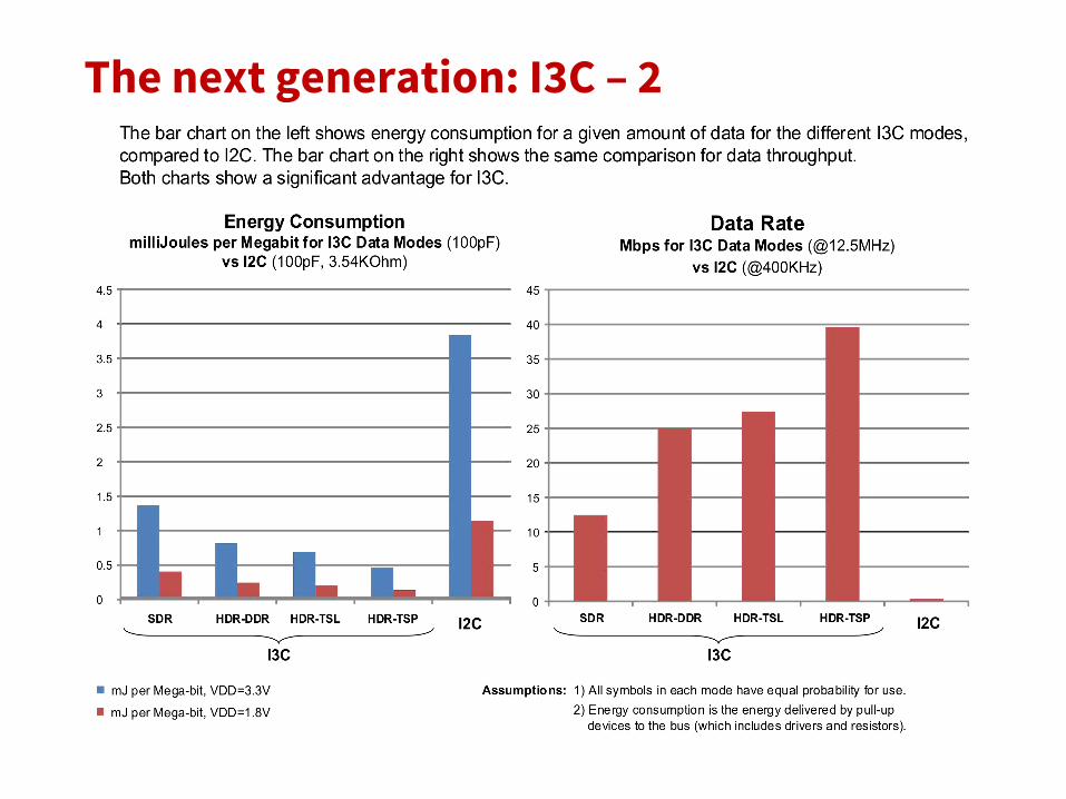
The next generation: I3C – 2

The next generation: I3C – 3

The next generation: I3C – 3
I2C backward compatible

The next generation: I3C – 3
I2C backward compatible
Similar to I2C, but dynamic address
The next generation: I3C – 3
I2C backward compatible
Similar to I2C, but dynamic address
Broadcast message
The next generation: I3C – 3
I2C backward compatible
Similar to I2C, but dynamic address
Broadcast message
High-Data Rate (SPI-like)
Yes, but how to actually use these interfaces?
• Now, we make a practical example• We’ll see a set of specific steps related to a specific STM32
microcontroller, but the concepts are general and adaptable to a wide range of MCUs

Yes, but how to actually use these interfaces?
• Now, we make a practical example• We’ll see a set of specific steps related to a specific STM32
microcontroller, but the concepts are general and adaptable to a wide range of MCUs
• The purpose of this example is to:1. Illustrate the procedure to use a peripheral interface in a real
microcontroller2. Show how to read technical documentation so that you can
replicate this feat in a practical situation
• The purpose of this example is not to teach the specific register names / numbers, etc.• So it’s not particularly useful to learn them by heart

Yes, but how to actually use these interfaces?- 2
• Our task is to use the third I2C interface (I2C3) on aSTM32-F401 microcontroller device
Yes, but how to actually use these interfaces?- 2
• Our task is to use the third I2C interface (I2C3) on aSTM32-F401 microcontroller device
• The steps shown here correspond to what you would do in C code using the STM32 Standard Peripheral Library (SPL)

Yes, but how to actually use these interfaces?- 2
• Our task is to use the third I2C interface (I2C3) on aSTM32-F401 microcontroller device
• The steps shown here correspond to what you would do in C code using the STM32 Standard Peripheral Library (SPL)• In practice, the SPL is actually easier to use than what we show here, as it
abstracts low level details (e.g. registers) using C data structures, functions.• Next week, a taste of how the Standard Peripheral Library works on a
simple case (blinking a LED).

Practical case: DocumentationThe information to use I2C (and in general the MCU) is typically contained in a datasheet:

Practical case: DocumentationThe information to use I2C (and in general the MCU) is typically contained in a datasheet:
And/or a reference manual:

Practical case: I2C on STM32-F401
DocID
024738 Rev 5
14/134
STM32F401xB STM
32F401xCDescription
53
Figure 3. STM32F401xB/STM
32F401xC block diagram
1.The tim
ers connected to AP
B2 are clocked from
TIMxC
LK up to 84 M
Hz, w
hile the timers connected to A
PB
1 are clocked from
TIMxC
LK up to 42
MH
z. *3,2�3257�$
$+%�$3%�
(;7�,7��:.83
XS�WR����$)�
3$>����@
7,0����3:
0��FRP
SO��FKDQQHOV�7,0�B&+�>���@1�
��FKDQQHOV�7,0�B&+�>���@(75�
%.,1�DV�$)
86$57�5;��7;��&.�
&76��576�DV�$)
63,�026,��0
,62�6&.��166�DV�$)
$3%����0+]
$3%����0+]
���DQDORJ�LQSXWV�
9''5()B$'&
026,�6'��0
,62�6'BH[W��6&.�&.166�:
6��0&.�DV�$)
63��,�6�
$/$50B287
26&��B,126&��B287
9''$��966$1567
VPFDUG
LU'$
��E
9%$7� ������WR�����9
'0$�
6&/��6'$��60%$�DV�$)
,�&��60%86
-7$*��6:�
$50�&RUWH[�0
�����0
+] �
19,&(70
038
75$&(&/.75$&('>���@
�
�
'0$�
��6WUHDPV
),)2
�$&&(/�&$&+(
�
$+%�����0+]
�
86$57��0%SV
7HPSHUDWXUH�VHQVRU
$'&�,)
#9''$
325�3'5%25
6XSSO\VXSHUYLVLRQ
#9''$ 39'
,QW
325�UHVHW
;7$/����N+]�
0$1$*7
57&
5&�+6
5&�/6
3:5
LQWHUIDFH
:'*���.
�#9%$7
#9''$
#9''
$:8
5HVHW�FORFNFRQWURO
3//��
$3%�&/.
9''� �����WR�����9
9669&$3
� 9ROWDJHUHJXODWRU
����WR�����9�
9''3RZHU�P
DQDJPW
#9''
67$03��
%DFNXS�UHJLVWHU�
$+%�EXV�PDWUL[��6�0� �
$3%�����0+]�
/6
7,0�
� ��FKDQQHOV�DV�$)�
)ODVKXS�WR�����.%
7,0�
7,0�
7,0�
7,0�
'�%86
06�����9�
�
)38
�$3%������0+]��PD[�
$+%�����0+]
1-7567��-7',�-7&.�6:
&/.-7'2�6:
'��-7'2
,�%86
6�%86
'0$�
��6WUHDPV
),)2
3%>����@
3&>����@
3+>���@
*3,2�3257�%
*3,2�3257�&
*3,2�3257�+��E
7,0��
��E
7,0��
��E
VPFDUG
LU'$86$57�
��FKDQQHO�DV�$)
��FKDQQHO�DV�$)
5;��7;��&.�DV�$)�,�&��60
%86
,�&��60%86
6&/��6'$��60%$�DV�$)
6&/��6'$��60%$�DV�$)
63��,�6�026,�6'��0
,62�6'BH[W��6&.�&.166�:
6��0&.�DV�$)
5;��7;�DV�$)&76��576�DV�$)
86$57� VPFDUGLU'$
��E
��E
��E
��E
��FKDQQHOV
��FKDQQHOV��(75�DV�$)
��FKDQQHOV��(75�DV�$)
��FKDQQHOV��(75�DV�$)
'0$�
$+%�$3%�
/6
26&B,126&B287
+&/.
;7$/�26&�����0
+]
65$0����.%
::'*
$3%�&/.
$+%�3&/.$+%�3&/.
&5&
�0$2
�/&&
����TO�����6�0$
2�/
.
3$)/
���--
#
&)&/
$;���=
#-
$��#+�AS�!&
53"
/4'
�&3
&)&/
0(9
$0
$-
)$��6"53��3/
&
63,�026,��0
,62�6&.��166�DV�$)
3'>����@*3,2�3257�'
3(>����@*3,2�3257�(
0. Understand the complexity!
core
I2C3

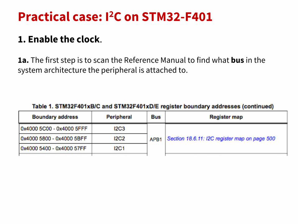
Practical case: I2C on STM32-F4011. Enable the clock.

Practical case: I2C on STM32-F4011. Enable the clock.
1a. The first step is to scan the Reference Manual to find what bus in the system architecture the peripheral is attached to.
Practical case: I2C on STM32-F4011. Enable the clock.
1a. The first step is to scan the Reference Manual to find what bus in the system architecture the peripheral is attached to.

Practical case: I2C on STM32-F4011. Enable the clock.
1a. The first step is to scan the Reference Manual to find what bus in the system architecture the peripheral is attached to.• In the example, the bus is APB1.

Practical case: I2C on STM32-F401
DocID
024738 Rev 5
14/134
STM32F401xB STM
32F401xCDescription
53
Figure 3. STM32F401xB/STM
32F401xC block diagram
1.The tim
ers connected to AP
B2 are clocked from
TIMxC
LK up to 84 M
Hz, w
hile the timers connected to A
PB
1 are clocked from
TIMxC
LK up to 42
MH
z. *3,2�3257�$
$+%�$3%�
(;7�,7��:.83
XS�WR����$)�
3$>����@
7,0����3:
0��FRP
SO��FKDQQHOV�7,0�B&+�>���@1�
��FKDQQHOV�7,0�B&+�>���@(75�
%.,1�DV�$)
86$57�5;��7;��&.�
&76��576�DV�$)
63,�026,��0
,62�6&.��166�DV�$)
$3%����0+]
$3%����0+]
���DQDORJ�LQSXWV�
9''5()B$'&
026,�6'��0
,62�6'BH[W��6&.�&.166�:
6��0&.�DV�$)
63��,�6�
$/$50B287
26&��B,126&��B287
9''$��966$1567
VPFDUG
LU'$
��E
9%$7� ������WR�����9
'0$�
6&/��6'$��60%$�DV�$)
,�&��60%86
-7$*��6:�
$50�&RUWH[�0
�����0
+] �
19,&(70
038
75$&(&/.75$&('>���@
�
�
'0$�
��6WUHDPV
),)2
�$&&(/�&$&+(
�
$+%�����0+]
�
86$57��0%SV
7HPSHUDWXUH�VHQVRU
$'&�,)
#9''$
325�3'5%25
6XSSO\VXSHUYLVLRQ
#9''$ 39'
,QW
325�UHVHW
;7$/����N+]�
0$1$*7
57&
5&�+6
5&�/6
3:5
LQWHUIDFH
:'*���.
�#9%$7
#9''$
#9''
$:8
5HVHW�FORFNFRQWURO
3//��
$3%�&/.
9''� �����WR�����9
9669&$3
� 9ROWDJHUHJXODWRU
����WR�����9�
9''3RZHU�P
DQDJPW
#9''
67$03��
%DFNXS�UHJLVWHU�
$+%�EXV�PDWUL[��6�0� �
$3%�����0+]�
/6
7,0�
� ��FKDQQHOV�DV�$)�
)ODVKXS�WR�����.%
7,0�
7,0�
7,0�
7,0�
'�%86
06�����9�
�
)38
�$3%������0+]��PD[�
$+%�����0+]
1-7567��-7',�-7&.�6:
&/.-7'2�6:
'��-7'2
,�%86
6�%86
'0$�
��6WUHDPV
),)2
3%>����@
3&>����@
3+>���@
*3,2�3257�%
*3,2�3257�&
*3,2�3257�+��E
7,0��
��E
7,0��
��E
VPFDUG
LU'$86$57�
��FKDQQHO�DV�$)
��FKDQQHO�DV�$)
5;��7;��&.�DV�$)�,�&��60
%86
,�&��60%86
6&/��6'$��60%$�DV�$)
6&/��6'$��60%$�DV�$)
63��,�6�026,�6'��0
,62�6'BH[W��6&.�&.166�:
6��0&.�DV�$)
5;��7;�DV�$)&76��576�DV�$)
86$57� VPFDUGLU'$
��E
��E
��E
��E
��FKDQQHOV
��FKDQQHOV��(75�DV�$)
��FKDQQHOV��(75�DV�$)
��FKDQQHOV��(75�DV�$)
'0$�
$+%�$3%�
/6
26&B,126&B287
+&/.
;7$/�26&�����0
+]
65$0����.%
::'*
$3%�&/.
$+%�3&/.$+%�3&/.
&5&
�0$2
�/&&
����TO�����6�0$
2�/
.
3$)/
���--
#
&)&/
$;���=
#-
$��#+�AS�!&
53"
/4'
�&3
&)&/
0(9
$0
$-
)$��6"53��3/
&
63,�026,��0
,62�6&.��166�DV�$)
3'>����@*3,2�3257�'
3(>����@*3,2�3257�(
core
I2C3
1. Enable the clock.
APB1
Practical case: I2C on STM32-F4011. Enable the clock.
1b. Then, you look at the clock tree diagram to understand what clocks should be active. The prescalers define the frequency of the peripheral clock.

Practical case: I2C on STM32-F4011. Enable the clock.
1b. Then, you look at the clock tree diagram to understand what clocks should be active. The prescalers define the frequency of the peripheral clock.

APB1 clk enable
Practical case: I2C on STM32-F4011. Enable the clock.
1b. Then, you look at the clock tree diagram to understand what clocks should be active. The prescalers define the frequency of the peripheral clock.

Practical case: I2C on STM32-F4011. Enable the clock.
1c. You enable the relevant clock(s) by setting a value in the right bit a memory-mapped reset/clock control (RCC) registers.

Practical case: I2C on STM32-F4011. Enable the clock.
1c. You enable the relevant clock(s) by setting a value in the right bit a memory-mapped reset/clock control (RCC) registers.

Practical case: I2C on STM32-F4011. Enable the clock.
1c. You enable the relevant clock(s) by setting a value in the right bit a memory-mapped reset/clock control (RCC) registers.• In the example, you set bit 23 of register RCC_APB1ENR to 1.

Practical case: I2C on STM32-F401
DocID
024738 Rev 5
14/134
STM32F401xB STM
32F401xCDescription
53
Figure 3. STM32F401xB/STM
32F401xC block diagram
1.The tim
ers connected to AP
B2 are clocked from
TIMxC
LK up to 84 M
Hz, w
hile the timers connected to A
PB
1 are clocked from
TIMxC
LK up to 42
MH
z. *3,2�3257�$
$+%�$3%�
(;7�,7��:.83
XS�WR����$)�
3$>����@
7,0����3:
0��FRP
SO��FKDQQHOV�7,0�B&+�>���@1�
��FKDQQHOV�7,0�B&+�>���@(75�
%.,1�DV�$)
86$57�5;��7;��&.�
&76��576�DV�$)
63,�026,��0
,62�6&.��166�DV�$)
$3%����0+]
$3%����0+]
���DQDORJ�LQSXWV�
9''5()B$'&
026,�6'��0
,62�6'BH[W��6&.�&.166�:
6��0&.�DV�$)
63��,�6�
$/$50B287
26&��B,126&��B287
9''$��966$1567
VPFDUG
LU'$
��E
9%$7� ������WR�����9
'0$�
6&/��6'$��60%$�DV�$)
,�&��60%86
-7$*��6:�
$50�&RUWH[�0
�����0
+] �
19,&(70
038
75$&(&/.75$&('>���@
�
�
'0$�
��6WUHDPV
),)2
�$&&(/�&$&+(
�
$+%�����0+]
�
86$57��0%SV
7HPSHUDWXUH�VHQVRU
$'&�,)
#9''$
325�3'5%25
6XSSO\VXSHUYLVLRQ
#9''$ 39'
,QW
325�UHVHW
;7$/����N+]�
0$1$*7
57&
5&�+6
5&�/6
3:5
LQWHUIDFH
:'*���.
�#9%$7
#9''$
#9''
$:8
5HVHW�FORFNFRQWURO
3//��
$3%�&/.
9''� �����WR�����9
9669&$3
� 9ROWDJHUHJXODWRU
����WR�����9�
9''3RZHU�P
DQDJPW
#9''
67$03��
%DFNXS�UHJLVWHU�
$+%�EXV�PDWUL[��6�0� �
$3%�����0+]�
/6
7,0�
� ��FKDQQHOV�DV�$)�
)ODVKXS�WR�����.%
7,0�
7,0�
7,0�
7,0�
'�%86
06�����9�
�
)38
�$3%������0+]��PD[�
$+%�����0+]
1-7567��-7',�-7&.�6:
&/.-7'2�6:
'��-7'2
,�%86
6�%86
'0$�
��6WUHDPV
),)2
3%>����@
3&>����@
3+>���@
*3,2�3257�%
*3,2�3257�&
*3,2�3257�+��E
7,0��
��E
7,0��
��E
VPFDUG
LU'$86$57�
��FKDQQHO�DV�$)
��FKDQQHO�DV�$)
5;��7;��&.�DV�$)�,�&��60
%86
,�&��60%86
6&/��6'$��60%$�DV�$)
6&/��6'$��60%$�DV�$)
63��,�6�026,�6'��0
,62�6'BH[W��6&.�&.166�:
6��0&.�DV�$)
5;��7;�DV�$)&76��576�DV�$)
86$57� VPFDUGLU'$
��E
��E
��E
��E
��FKDQQHOV
��FKDQQHOV��(75�DV�$)
��FKDQQHOV��(75�DV�$)
��FKDQQHOV��(75�DV�$)
'0$�
$+%�$3%�
/6
26&B,126&B287
+&/.
;7$/�26&�����0
+]
65$0����.%
::'*
$3%�&/.
$+%�3&/.$+%�3&/.
&5&
�0$2
�/&&
����TO�����6�0$
2�/
.
3$)/
���--
#
&)&/
$;���=
#-
$��#+�AS�!&
53"
/4'
�&3
&)&/
0(9
$0
$-
)$��6"53��3/
&
63,�026,��0
,62�6&.��166�DV�$)
3'>����@*3,2�3257�'
3(>����@*3,2�3257�(
core
I2C3
1. Enable the clock.
RCC

Practical case: I2C on STM32-F4012. Connect the pins to the correct function.

Practical case: I2C on STM32-F4012. Connect the pins to the correct function.
2a. You check which pins are associated to the interface you want to use.

Practical case: I2C on STM32-F4012. Connect the pins to the correct function.
2a. You check which pins are associated to the interface you want to use.

Practical case: I2C on STM32-F4012. Connect the pins to the correct function.
2a. You check which pins are associated to the interface you want to use.• In the example, the I2C3 interface uses pins C9 (for SDA) and A8 (for SCL).

Practical case: I2C on STM32-F4012. Connect the pins to the correct function.
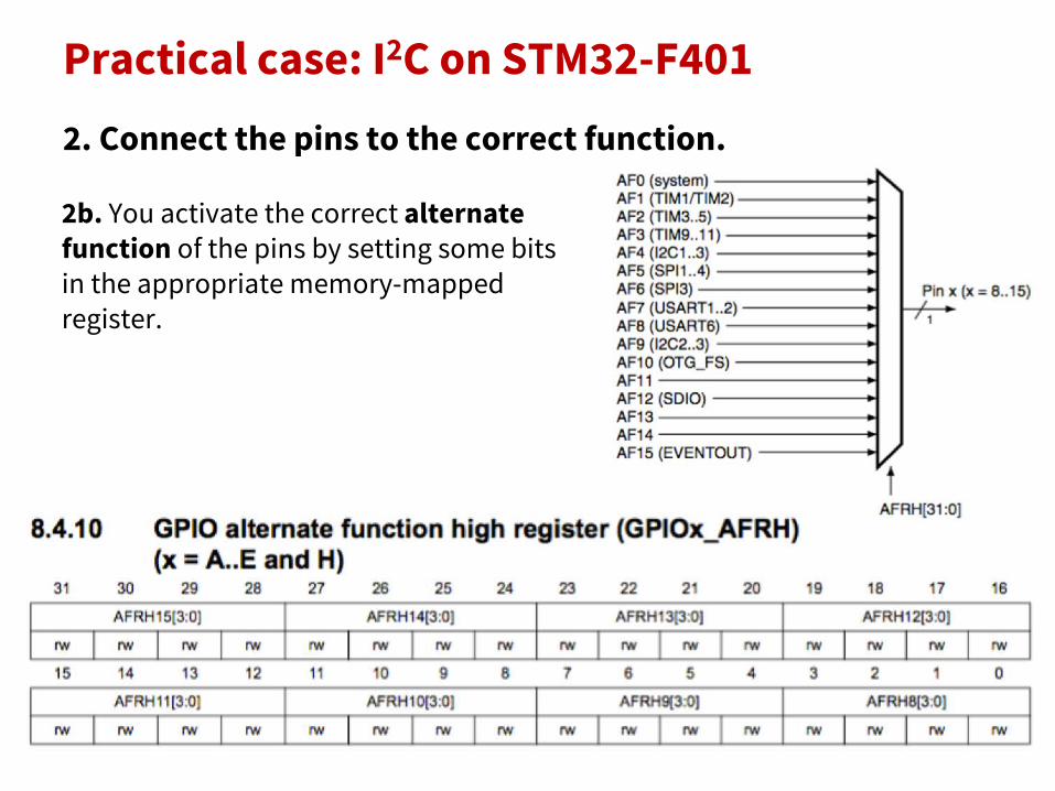
2b. You activate the correct alternate function of the pins by setting some bits in the appropriate memory-mapped register.
Practical case: I2C on STM32-F4012. Connect the pins to the correct function.
2b. You activate the correct alternate function of the pins by setting some bits in the appropriate memory-mapped register.

Practical case: I2C on STM32-F4012. Connect the pins to the correct function.
2b. You activate the correct alternate function of the pins by setting some bits in the appropriate memory-mapped register.• In the example, you set both the AFHR9
bit field of register GPIOC_AFRH and the AFHR8 bit field of register GPIOA_AFRH to function 4 (4’b1000)
Practical case: I2C on STM32-F401
DocID
024738 Rev 5
14/134
STM32F401xB STM
32F401xCDescription
53
Figure 3. STM32F401xB/STM
32F401xC block diagram
1.The tim
ers connected to AP
B2 are clocked from
TIMxC
LK up to 84 M
Hz, w
hile the timers connected to A
PB
1 are clocked from
TIMxC
LK up to 42
MH
z. *3,2�3257�$
$+%�$3%�
(;7�,7��:.83
XS�WR����$)�
3$>����@
7,0����3:
0��FRP
SO��FKDQQHOV�7,0�B&+�>���@1�
��FKDQQHOV�7,0�B&+�>���@(75�
%.,1�DV�$)
86$57�5;��7;��&.�
&76��576�DV�$)
63,�026,��0
,62�6&.��166�DV�$)
$3%����0+]
$3%����0+]
���DQDORJ�LQSXWV�
9''5()B$'&
026,�6'��0
,62�6'BH[W��6&.�&.166�:
6��0&.�DV�$)
63��,�6�
$/$50B287
26&��B,126&��B287
9''$��966$1567
VPFDUG
LU'$
��E
9%$7� ������WR�����9
'0$�
6&/��6'$��60%$�DV�$)
,�&��60%86
-7$*��6:�
$50�&RUWH[�0
�����0
+] �
19,&(70
038
75$&(&/.75$&('>���@
�
�
'0$�
��6WUHDPV
),)2
�$&&(/�&$&+(
�
$+%�����0+]
�
86$57��0%SV
7HPSHUDWXUH�VHQVRU
$'&�,)
#9''$
325�3'5%25
6XSSO\VXSHUYLVLRQ
#9''$ 39'
,QW
325�UHVHW
;7$/����N+]�
0$1$*7
57&
5&�+6
5&�/6
3:5
LQWHUIDFH
:'*���.
�#9%$7
#9''$
#9''
$:8
5HVHW�FORFNFRQWURO
3//��
$3%�&/.
9''� �����WR�����9
9669&$3
� 9ROWDJHUHJXODWRU
����WR�����9�
9''3RZHU�P
DQDJPW
#9''
67$03��
%DFNXS�UHJLVWHU�
$+%�EXV�PDWUL[��6�0� �
$3%�����0+]�
/6
7,0�
� ��FKDQQHOV�DV�$)�
)ODVKXS�WR�����.%
7,0�
7,0�
7,0�
7,0�
'�%86
06�����9�
�
)38
�$3%������0+]��PD[�
$+%�����0+]
1-7567��-7',�-7&.�6:
&/.-7'2�6:
'��-7'2
,�%86
6�%86
'0$�
��6WUHDPV
),)2
3%>����@
3&>����@
3+>���@
*3,2�3257�%
*3,2�3257�&
*3,2�3257�+��E
7,0��
��E
7,0��
��E
VPFDUG
LU'$86$57�
��FKDQQHO�DV�$)
��FKDQQHO�DV�$)
5;��7;��&.�DV�$)�,�&��60
%86
,�&��60%86
6&/��6'$��60%$�DV�$)
6&/��6'$��60%$�DV�$)
63��,�6�026,�6'��0
,62�6'BH[W��6&.�&.166�:
6��0&.�DV�$)
5;��7;�DV�$)&76��576�DV�$)
86$57� VPFDUGLU'$
��E
��E
��E
��E
��FKDQQHOV
��FKDQQHOV��(75�DV�$)
��FKDQQHOV��(75�DV�$)
��FKDQQHOV��(75�DV�$)
'0$�
$+%�$3%�
/6
26&B,126&B287
+&/.
;7$/�26&�����0
+]
65$0����.%
::'*
$3%�&/.
$+%�3&/.$+%�3&/.
&5&
�0$2
�/&&
����TO�����6�0$
2�/
.
3$)/
���--
#
&)&/
$;���=
#-
$��#+�AS�!&
53"
/4'
�&3
&)&/
0(9
$0
$-
)$��6"53��3/
&
63,�026,��0
,62�6&.��166�DV�$)
3'>����@*3,2�3257�'
3(>����@*3,2�3257�(
core
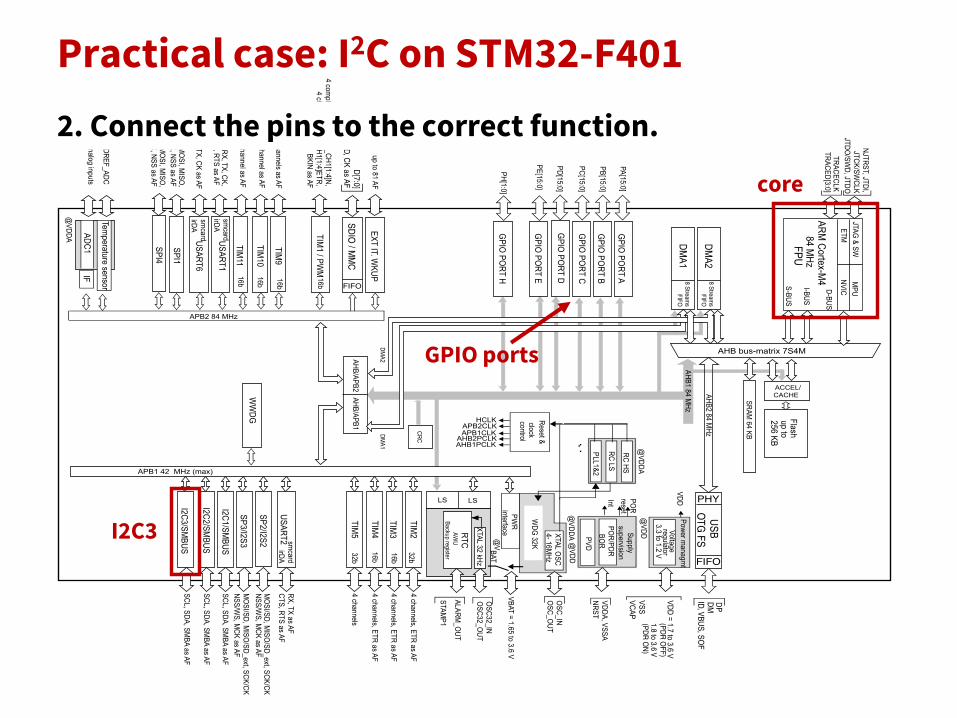
I2C3
2. Connect the pins to the correct function.
GPIO ports

Practical case: I2C on STM32-F4013. Configure the peripheral interface.
Practical case: I2C on STM32-F4013. Configure the peripheral interface.
3a. You write the peripheral memory-mapped control registers.

Practical case: I2C on STM32-F4013. Configure the peripheral interface.
3a. You write the peripheral memory-mapped control registers.

Practical case: I2C on STM32-F4013. Configure the peripheral interface.
3a. You write the peripheral memory-mapped control registers.• In the example, you can allow or disallow clock stretching (plus other options).
The I2C3 peripheral must also know the APB1 clock frequency, therefore you must set it in the FREQ bit field.

Practical case: I2C on STM32-F4013. Configure the peripheral interface.
3b. You configure the SCL clock.
Practical case: I2C on STM32-F4013. Configure the peripheral interface.
3b. You configure the SCL clock.

Practical case: I2C on STM32-F4013. Configure the peripheral interface.
3b. You configure the SCL clock.• In the example, you can set the SCL clock to a submultiple frequency of the APB1
clock in the I2C_CCR register.
Practical case: I2C on STM32-F4014. Start the transfer.

Practical case: I2C on STM32-F4014. Start the transfer.
4a. You start the transfer by setting a start bit.

Practical case: I2C on STM32-F4014. Start the transfer.
4a. You start the transfer by setting a start bit.

Practical case: I2C on STM32-F4014. Start the transfer.
4a. You start the transfer by setting a start bit.• In the example, you set the START bit of the I2C_CR1 register to 1.

Practical case: I2C on STM32-F4014. Start the transfer.
4b. You check the status.
Practical case: I2C on STM32-F4014. Start the transfer.
4b. You check the status.

Practical case: I2C on STM32-F4014. Start the transfer.
4b. You check the status.• In the example, you read the I2C_SR1 register (this is required by the I2C
peripheral in the STM32F401).

Practical case: I2C on STM32-F4014. Start the transfer.
4c. You configure I2C address and direction.

Practical case: I2C on STM32-F4014. Start the transfer.
4c. You configure I2C address and direction.
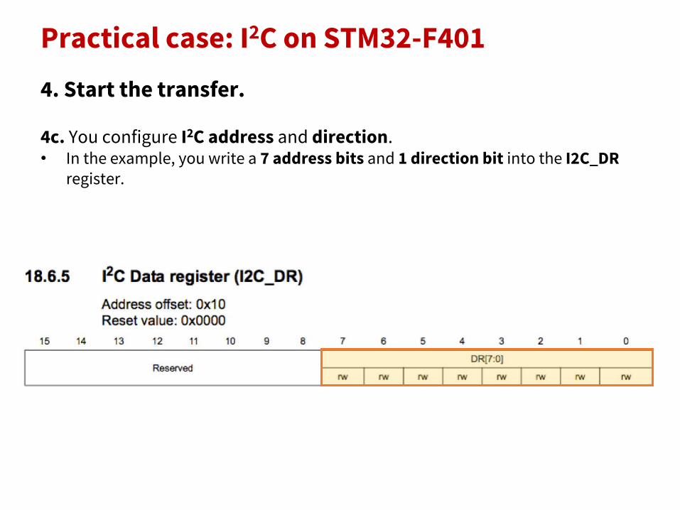
Practical case: I2C on STM32-F4014. Start the transfer.
4c. You configure I2C address and direction.• In the example, you write a 7 address bits and 1 direction bit into the I2C_DR
register.

Practical case: I2C on STM32-F4015. Perform the transfer.

Practical case: I2C on STM32-F4015. Perform the transfer.
You read or write data packets in the I2C interface.

Practical case: I2C on STM32-F4015. Perform the transfer.
You read or write data packets in the I2C interface.

Practical case: I2C on STM32-F4015. Perform the transfer.
You read or write data packets in the I2C interface.• In the example, you read/write one byte at a time from/into the I2C_DR
register.

Practical case: I2C on STM32-F4016. End the transfer.
Practical case: I2C on STM32-F4016. End the transfer.
You end the transfer by setting an appropriate value in the control register.

Practical case: I2C on STM32-F4016. End the transfer.
You end the transfer by setting an appropriate value in the control register.

Practical case: I2C on STM32-F4016. End the transfer.
You end the transfer by setting an appropriate value in the control register.• In the example, in case of a read you have to clear the ACK bit to 0. In case of a
write, you have to set the STOP bit to 1.

Practical case: I2C on STM32-F401
DocID
024738 Rev 5
14/134
STM32F401xB STM
32F401xCDescription
53
Figure 3. STM32F401xB/STM
32F401xC block diagram
1.The tim
ers connected to AP
B2 are clocked from
TIMxC
LK up to 84 M
Hz, w
hile the timers connected to A
PB
1 are clocked from
TIMxC
LK up to 42
MH
z. *3,2�3257�$
$+%�$3%�
(;7�,7��:.83
XS�WR����$)�
3$>����@
7,0����3:
0��FRP
SO��FKDQQHOV�7,0�B&+�>���@1�
��FKDQQHOV�7,0�B&+�>���@(75�
%.,1�DV�$)
86$57�5;��7;��&.�
&76��576�DV�$)
63,�026,��0
,62�6&.��166�DV�$)
$3%����0+]
$3%����0+]
���DQDORJ�LQSXWV�
9''5()B$'&
026,�6'��0
,62�6'BH[W��6&.�&.166�:
6��0&.�DV�$)
63��,�6�
$/$50B287
26&��B,126&��B287
9''$��966$1567
VPFDUG
LU'$
��E
9%$7� ������WR�����9
'0$�
6&/��6'$��60%$�DV�$)
,�&��60%86
-7$*��6:�
$50�&RUWH[�0
�����0
+] �
19,&(70
038
75$&(&/.75$&('>���@
�
�
'0$�
��6WUHDPV
),)2
�$&&(/�&$&+(
�
$+%�����0+]
�
86$57��0%SV
7HPSHUDWXUH�VHQVRU
$'&�,)
#9''$
325�3'5%25
6XSSO\VXSHUYLVLRQ
#9''$ 39'
,QW
325�UHVHW
;7$/����N+]�
0$1$*7
57&
5&�+6
5&�/6
3:5
LQWHUIDFH
:'*���.
�#9%$7
#9''$
#9''
$:8
5HVHW�FORFNFRQWURO
3//��
$3%�&/.
9''� �����WR�����9
9669&$3
� 9ROWDJHUHJXODWRU
����WR�����9�
9''3RZHU�P
DQDJPW
#9''
67$03��
%DFNXS�UHJLVWHU�
$+%�EXV�PDWUL[��6�0� �
$3%�����0+]�
/6
7,0�
� ��FKDQQHOV�DV�$)�
)ODVKXS�WR�����.%
7,0�
7,0�
7,0�
7,0�
'�%86
06�����9�
�
)38
�$3%������0+]��PD[�
$+%�����0+]
1-7567��-7',�-7&.�6:
&/.-7'2�6:
'��-7'2
,�%86
6�%86
'0$�
��6WUHDPV
),)2
3%>����@
3&>����@
3+>���@
*3,2�3257�%
*3,2�3257�&
*3,2�3257�+��E
7,0��
��E
7,0��
��E
VPFDUG
LU'$86$57�
��FKDQQHO�DV�$)
��FKDQQHO�DV�$)
5;��7;��&.�DV�$)�,�&��60
%86
,�&��60%86
6&/��6'$��60%$�DV�$)
6&/��6'$��60%$�DV�$)
63��,�6�026,�6'��0
,62�6'BH[W��6&.�&.166�:
6��0&.�DV�$)
5;��7;�DV�$)&76��576�DV�$)
86$57� VPFDUGLU'$
��E
��E
��E
��E
��FKDQQHOV
��FKDQQHOV��(75�DV�$)
��FKDQQHOV��(75�DV�$)
��FKDQQHOV��(75�DV�$)
'0$�
$+%�$3%�
/6
26&B,126&B287
+&/.
;7$/�26&�����0
+]
65$0����.%
::'*
$3%�&/.
$+%�3&/.$+%�3&/.
&5&
�0$2
�/&&
����TO�����6�0$
2�/
.
3$)/
���--
#
&)&/
$;���=
#-
$��#+�AS�!&
53"
/4'
�&3
&)&/
0(9
$0
$-
)$��6"53��3/
&
63,�026,��0
,62�6&.��166�DV�$)
3'>����@*3,2�3257�'
3(>����@*3,2�3257�(
7. What you’d do for real…
core
I2C3
DMAengine
SRAM
int