Embed Size (px)
Citation preview
Application Note Using the Cortex-M3 on the Microcontroller Prototyping
System
Document number: ARM DAI0218A
Issued: February 2009
Copyright ARM Limited 2009
218
ii Copyright © 2009 ARM Limited. All rights reserved. Application Note 218 ARM DAI0218A
Application Note 218 Using the Cortex-M3 on the Microcontroller Prototyping System Copyright © 2009 ARM Limited. All rights reserved.
Release information
The following changes have been made to this Application Note.
Change history
Date Issue Change
February 2009 A First release
Version controlled by Domino.Doc DS158-GENC-009371 2.3
References
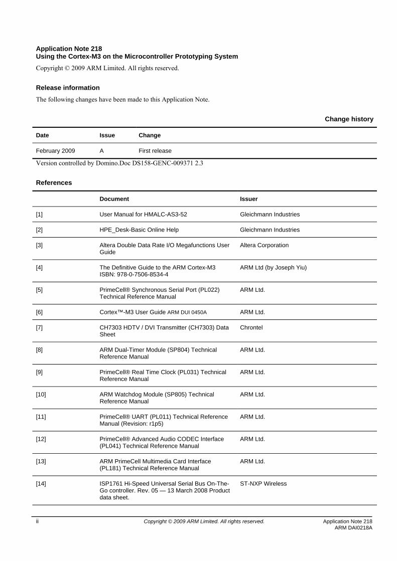
Document Issuer
[1] User Manual for HMALC-AS3-52 Gleichmann Industries
[2] HPE_Desk-Basic Online Help Gleichmann Industries
[3] Altera Double Data Rate I/O Megafunctions User Guide
Altera Corporation
[4] The Definitive Guide to the ARM Cortex-M3 ISBN: 978-0-7506-8534-4
ARM Ltd (by Joseph Yiu)
[5] PrimeCell® Synchronous Serial Port (PL022) Technical Reference Manual
ARM Ltd.
[6] Cortex™-M3 User Guide ARM DUI 0450A ARM Ltd.
[7] CH7303 HDTV / DVI Transmitter (CH7303) Data Sheet
Chrontel
[8] ARM Dual-Timer Module (SP804) Technical Reference Manual
ARM Ltd.
[9] PrimeCell® Real Time Clock (PL031) Technical Reference Manual
ARM Ltd.
[10] ARM Watchdog Module (SP805) Technical Reference Manual
ARM Ltd.
[11] PrimeCell® UART (PL011) Technical Reference Manual (Revision: r1p5)
ARM Ltd.
[12] PrimeCell® Advanced Audio CODEC Interface (PL041) Technical Reference Manual
ARM Ltd.
[13] ARM PrimeCell Multimedia Card Interface (PL181) Technical Reference Manual
ARM Ltd.
[14] ISP1761 Hi-Speed Universal Serial Bus On-The-Go controller. Rev. 05 — 13 March 2008 Product data sheet.
ST-NXP Wireless
Application Note 218 Copyright © 2006 ARM Limited. All rights reserved. iii ARM DAI 0125A
Proprietary notice
ARM, the ARM Powered logo, Thumb and StrongARM are registered trademarks of ARM Limited. The ARM logo, AMBA, Angel, ARMulator, EmbeddedICE, ModelGen, Multi-ICE, ARM7TDMI, ARM9TDMI, TDMI and STRONG are trademarks of ARM Limited. All other products, or services, mentioned herein may be trademarks of their respective owners.
Confidentiality status
This document is Open Access. This document has no restriction on distribution.
Feedback on this Application Note If you have any comments on this Application Note, please send email to [email protected] giving: • the document title
• the document number
• the page number(s) to which your comments refer
• an explanation of your comments. General suggestions for additions and improvements are also welcome.
ARM web address
http://www.arm.com
iv Copyright © 2009 ARM Limited. All rights reserved. Application Note 218 ARM DAI0218A
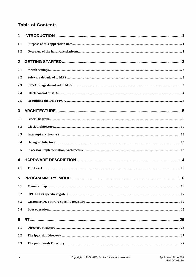
Table of Contents
1 INTRODUCTION ..................................................................................................................1
1.1 Purpose of this application note.................................................................................................................................... 1
1.2 Overview of the hardware platform............................................................................................................................. 1
2 GETTING STARTED............................................................................................................3
2.1 Switch settings ................................................................................................................................................................ 3
2.2 Software download to MPS........................................................................................................................................... 3
2.3 FPGA Image download to MPS.................................................................................................................................... 3
2.4 Clock control of MPS..................................................................................................................................................... 4
2.5 Rebuilding the DUT FPGA ........................................................................................................................................... 4
3 ARCHITECTURE .................................................................................................................5
3.1 Block Diagram................................................................................................................................................................ 5
3.2 Clock architecture........................................................................................................................................................ 10
3.3 Interrupt architecture ................................................................................................................................................. 13
3.4 Debug architecture....................................................................................................................................................... 13
3.5 Processor Implementation Architecture. ................................................................................................................... 13
4 HARDWARE DESCRIPTION.............................................................................................14
4.1 Top Level ...................................................................................................................................................................... 15
5 PROGRAMMER’S MODEL................................................................................................16
5.1 Memory map ................................................................................................................................................................ 16
5.2 CPU FPGA specific registers ...................................................................................................................................... 17
5.3 Customer DUT FPGA Specific Registers .................................................................................................................. 19
5.4 Boot operation .............................................................................................................................................................. 25
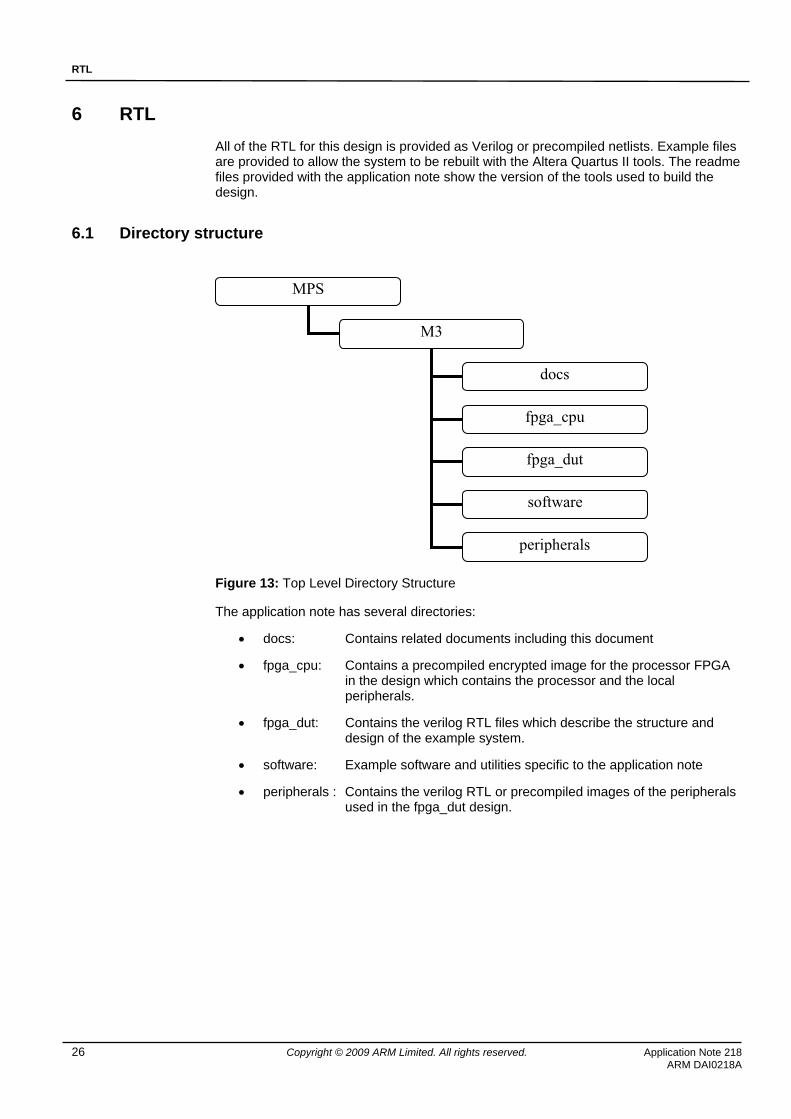
6 RTL.....................................................................................................................................26
6.1 Directory structure ...................................................................................................................................................... 26
6.2 The fpga_dut Directory ............................................................................................................................................... 27
6.3 The peripherals Directory........................................................................................................................................... 27
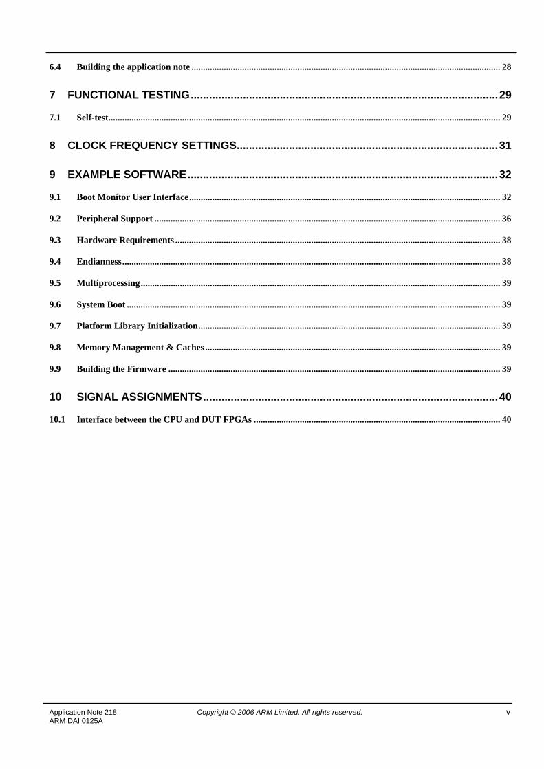
Application Note 218 Copyright © 2006 ARM Limited. All rights reserved. v ARM DAI 0125A
6.4 Building the application note ...................................................................................................................................... 28
7 FUNCTIONAL TESTING....................................................................................................29
7.1 Self-test.......................................................................................................................................................................... 29
8 CLOCK FREQUENCY SETTINGS.....................................................................................31
9 EXAMPLE SOFTWARE.....................................................................................................32
9.1 Boot Monitor User Interface....................................................................................................................................... 32
9.2 Peripheral Support ...................................................................................................................................................... 36
9.3 Hardware Requirements ............................................................................................................................................. 38
9.4 Endianness.................................................................................................................................................................... 38
9.5 Multiprocessing............................................................................................................................................................ 39
9.6 System Boot .................................................................................................................................................................. 39
9.7 Platform Library Initialization................................................................................................................................... 39
9.8 Memory Management & Caches ................................................................................................................................ 39
9.9 Building the Firmware ................................................................................................................................................ 39
10 SIGNAL ASSIGNMENTS................................................................................................40
10.1 Interface between the CPU and DUT FPGAs ........................................................................................................... 40

Introduction
Application Note 218 Copyright © 2009 ARM Limited. All rights reserved. 1 ARM DAI0218A
1 Introduction
1.1 Purpose of this application note This application note covers the operation of the Hpe®_midiv2 with the HM-ALC-AS3 from Gleichmann Electronics Research. It describes the contents of the FPGAs on the HMALC-AS3-52, the system interconnect, the clock structure, and specifics of the programmer’s model relevant to Customer FPGA’s operation.
After reading this Application Note the user should be in a position to make changes to the customer FPGA design provided or introduce their own AHB based peripherals.
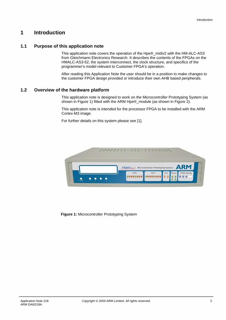
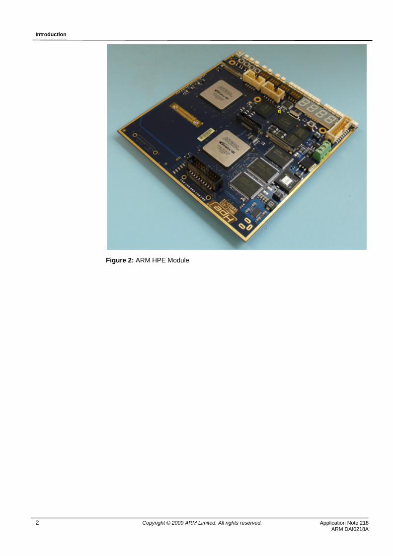
1.2 Overview of the hardware platform This application note is designed to work on the Microcontroller Prototyping System (as shown in Figure 1) fitted with the ARM Hpe®_module (as shown in Figure 2).
This application note is intended for the processor FPGA to be installed with the ARM Cortex-M3 image.
For further details on this system please see [1].
Figure 1: Microcontroller Prototyping System
Introduction
2 Copyright © 2009 ARM Limited. All rights reserved. Application Note 218 ARM DAI0218A
Figure 2: ARM HPE Module
Getting started
Application Note 218 Copyright © 2009 ARM Limited. All rights reserved. 3 ARM DAI0218A
2 Getting started The system comes pre-configured with an example design installed on the customer FPGA. The processor FPGA is configured and ready for use and the bootmonitor software is loaded into the system memory.
Connect a serial cable to RS232-4 (UART port3 above the power connector) and use a terminal emulation program (e.g. HyperTerminal) configured as 38,400 baud, 8bit data, no parity, 1 stop bit and no flow control to talk to the MPS. Insert the power cable and turn on the PWR switch at the back. This will bring up the system and the bootmonitor will start execution. The character display will show the Firmware (F/W) and Hardware (H/W) versions of the system. This is also output to the serial port for display on the terminal if connected. The CPU LEDs (0 to 7) will cycle a lighted bit to show the bootmonitor is running.
The three blue LEDs on the right will be lit to indicate that the system and FPGAs are configured with valid images. The four green Power LEDs will light to show all power supplies are functioning properly and within tolerance.
If a FAN LED lights then the corresponding FPGA temperature is above the pre-defined limit (if fans are fitted then the fan for that FPGA will become operational).
Pressing the recessed reset button on the front panel will perform a hardware reset and the system will restart as if it had been power cycled.
2.1 Switch settings The bootmonitor reads the processor switches 1-3 on power up and uses these to select the boot option. On delivery all the switches are set to ON and defaults to no boot script with auto detection of semihosting or UART port3 for console interface.
SW1 SW2 SW3 Function Note ON X X Normal boot Use this as default OFF X X Run boot Script This needs to be pre configured from the boot
monitor command line X ON ON Auto Select between UART port3
and Semihosting for Console Detects semihosting supported debugger
X ON OFF Force UART port3 for Console Always use UART port3 regardless of semihosting support
X OFF ON Reserved Do not use, undefined behaviour X OFF OFF Reserved Do not use, undefined behaviour
2.2 Software download to MPS The MPS comes with a Keil ULINK2 USB JTAG adaptor to allow download and programming of the Flash memory from µVision. The ULINK2 plugs into the 20way IDC connector at the back of the unit. Example software and projects are supplied for µVision. See the µVision documentation for details about how to compile and program the flash.
If you do not use the JTAG download it is possible to transfer files and write them into flash using bootmonitor and the SD-card slot.
It is possible to fit a SDCard or MMC into the SD-Card slot in the back and access it as a standard FAT16 8.3 filename device (long filenames are not supported and the maximum usable card size is 2GB).
2.3 FPGA Image download to MPS The HPE_Desk application (Windows based) from Gleichmann allows you to download new FPGA images for the DUT FPGA and updates from ARM for the CPU FPGA (when available). Please see the Hpe®_desk documentation for details on how to do this.
Getting started
4 Copyright © 2009 ARM Limited. All rights reserved. Application Note 218 ARM DAI0218A
2.4 Clock control of MPS HPE_Desk allows you to select which clock sources are routed to which clock inputs of the FPGAs (clock factory) so you can change the operation frequency of both the CPU and DUT FPGAs. The Clocks to the clock factory are driven from the DUT and CPU FPGAs. the CPU FPGA clocks are fixed by the design and not alterable by the customer. The DUT FPGA clocks are alterable by the user by reconfiguring the PLL used to generate them. Refer to the Altera Stratix III documentation for details on configuration of the PLL.
2.5 Rebuilding the DUT FPGA To rebuild the DUT FPGA and configuring the MPS please see section 6.4.
Architecture
Application Note 218 Copyright © 2009 ARM Limited. All rights reserved. 5 ARM DAI0218A
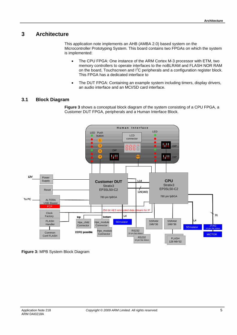
3 Architecture This application note implements an AHB (AMBA 2.0) based system on the Microcontroller Prototyping System. This board contains two FPGAs on which the system is implemented:
• The CPU FPGA: One instance of the ARM Cortex M-3 processor with ETM, two memory controllers to operate interfaces to the noBLRAM and FLASH NOR RAM on the board, Touchscreen and I2C peripherals and a configuration register block. This FPGA has a dedicated interface to
• The DUT FPGA: Containing an example system including timers, display drivers, an audio interface and an MCI/SD card interface.
3.1 Block Diagram Figure 3 shows a conceptual block diagram of the system consisting of a CPU FPGA, a Customer DUT FPGA, peripherals and a Human Interface Block.
FCPFCPFCP
Reset
ALTERAUSB Blaster
PowerSupply
12V
To PC
Reset
ALTERAUSB Blaster
PowerSupply
12V
Reset
ALTERAUSB Blaster
PowerSupplyPowerSupply
12V
To PC
256 bit AES encrypted data stream for IP
Common Conf FLASH
FLASH Handler
ClockFactory
Common Conf FLASH
FLASH Handler
ClockFactory 31
SEmulator
L4
L4
JTAG10 pin flat ribbon
MICTOR
SEmulator
31
SEmulatorSEmulator
L4
L4
JTAG10 pin flat ribbon
MICTORMICTOR
SEmulatorSEmulator
Hpe_moduleConnector
Hpe_moduleConnector
Hpe_childConnector
bottomtop
Customer DUTStratix3
EP3SL50-C2
780 pin fpBGA
DDR2 possible Hpe_moduleConnector
Hpe_moduleConnector
Hpe_moduleConnector
Hpe_childConnector
bottomtop
Customer DUTStratix3
EP3SL50-C2
780 pin fpBGA
DDR2 possible
Hpe_moduleConnector
Hpe_moduleConnector
Hpe_childConnector Hpe_childConnector
bottomtop
Customer DUTStratix3
EP3SL50-C2
780 pin fpBGA
DDR2 possible
126(182)
L14 CPUStratix3
EP3SL50-C2
780 pin fpBGA
126(182)
L14 CPUStratix3
EP3SL50-C2
780 pin fpBGA
SSRAM1Mb*36
FLASH128 Mb*32
SSRAM1Mb*36
SSRAM1Mb*36SSRAM1Mb*36
FLASH128 Mb*32
FLASH128 Mb*32
SSRAM1Mb*36SSRAM1Mb*36
RS23210 pin flat ribbon
RS23210 pin flat ribbon
RS23210 pin flat ribbon
RS23210 pin flat ribbon
RS23210 pin flat ribbon
RS23210 pin flat ribbon
H u m a n I n t e r f a c e
Pushbutton
LED
DIPDIP
LED
1
2
3
4 RES
LCDconnector
DIP
H u m a n I n t e r f a c e
Pushbutton
LED
DIPDIP
LED
1
2
3
4 RES
LCDconnector
DIP
Figure 3: MPB System Block Diagram
Architecture
6 Copyright © 2009 ARM Limited. All rights reserved. Application Note 218 ARM DAI0218A
BaseBoard
Processorboard
DUT FPGACPU FPGA
NOR
SSRAMSSRAM
DDR USB
Video
SMBSMB
Video DMB SMB
TraceDebug
UARTS
CharLCD
AC97 I2C SPISD/MMC
7SEGLEDsSwitchesLEDsSwitches
AHB Lite
Interrupts
Ethernet
I/O
I/O Ethernet
Video I/F
I/O
Trace/JTAG
MPB-M3 Block Diagram I/O
CAN
I/O
Flexray Lin
Not Implemented
Implemented
UART
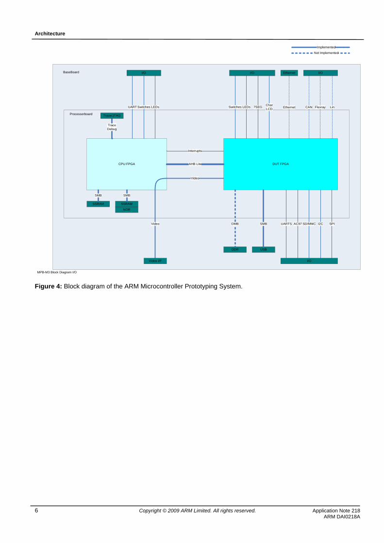
Figure 4: Block diagram of the ARM Microcontroller Prototyping System.
Architecture
Application Note 218 Copyright © 2009 ARM Limited. All rights reserved. 7 ARM DAI0218A
Bus architecture
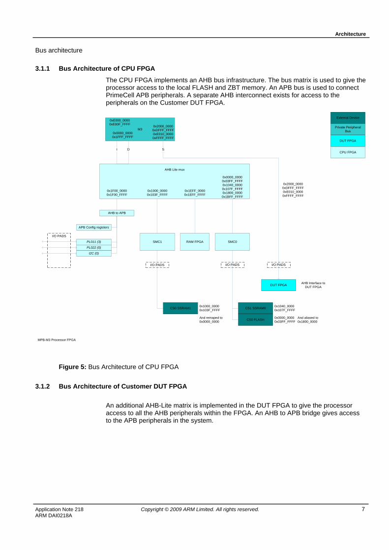
3.1.1 Bus Architecture of CPU FPGA
The CPU FPGA implements an AHB bus infrastructure. The bus matrix is used to give the processor access to the local FLASH and ZBT memory. An APB bus is used to connect PrimeCell APB peripherals. A separate AHB interconnect exists for access to the peripherals on the Customer DUT FPGA.
M3
AHB Lite mux
SMC1 SMC0
I
CS0 SSRAM1 CS1 SSRAM0
CS0 FLASH 0x0000_0000 0x03FF_FFFF
0x1040_0000 0x107F_FFFF
0x1F00_0000 0x1F00_FFFF
0x0000_0000 0x03FF_FFFF0x1040_00000x107F_FFFF0x1800_00000x1BFF_FFFF
APB Config registers
MPB-M3 Processor FPGA
I/O PADS
0xE000_00000xE00F_FFFF
0x1000_0000 0x103F_FFFF
D S
I/O PADSI/O PADS
0x0000_0000 0x1FFF_FFFF
RAM FPGA
0x1EFF_0000 0x1EFF_FFFF
And remaped to 0x0000_0000
And aliased to 0x1800_0000
0x2000_0000 0xDFFF_FFFF0xE010_00000xFFFF_FFFF
Private Peripheral Bus
DUT FPGA
CPU FPGA
External Device
DUT FPGA AHB Interface to DUT FPGA
0x2000_0000 0xDFFF_FFFF0xE010_00000xFFFF_FFFF
0x1000_0000 0x103F_FFFF
AHB to APB
PL011 (3)
PL022 (0)
I2C (0)
I/O PADS
Figure 5: Bus Architecture of CPU FPGA
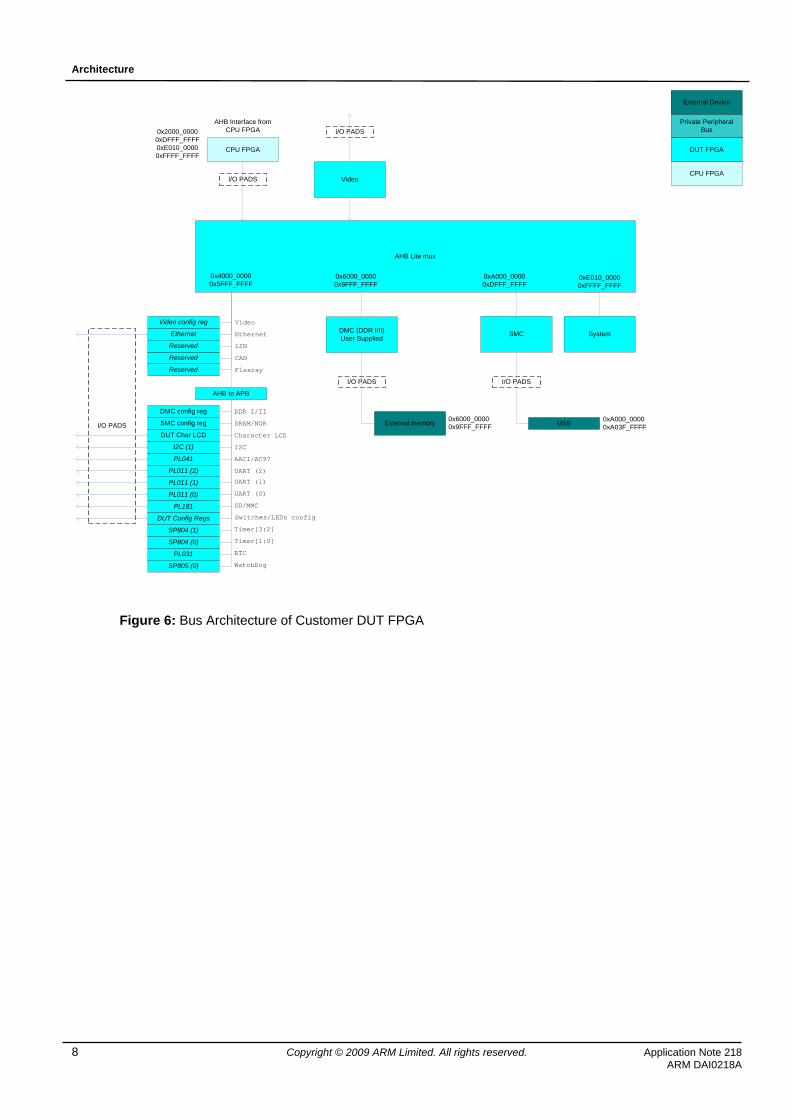
3.1.2 Bus Architecture of Customer DUT FPGA
An additional AHB-Lite matrix is implemented in the DUT FPGA to give the processor access to all the AHB peripherals within the FPGA. An AHB to APB bridge gives access to the APB peripherals in the system.
Architecture
8 Copyright © 2009 ARM Limited. All rights reserved. Application Note 218 ARM DAI0218A
AHB Lite mux
AHB to APB
SMC
0xA000_0000 0xDFFF_FFFF
0xE010_0000 0xFFFF_FFFF
AHB Interface from CPU FPGA
System
I/O PADS
0x4000_0000 0x5FFF_FFFF
I/O PADS
0x2000_0000 0xDFFF_FFFF0xE010_00000xFFFF_FFFF
0x6000_0000 0x9FFF_FFFF
Video
External memory 0xA000_0000 0xA03F_FFFF
I/O PADS
DMC (DDR I/II)User Supplied
I/O PADS
USB0x6000_0000 0x9FFF_FFFF
Ethernet
Video config reg
WatchDog
Timer[1:0]
Timer[3:2]
Flexray
CAN
LIN
RTC
I2C
UART (0)
UART (1)
SD/MMC
AACI/AC97
Video
Ethernet
I/O PADS
PL041
PL031
I2C (1)
PL011 (0)
SP805 (0)
SP804 (0)
SP804 (1)
PL011 (1)
PL181
DUT Config Regs
DUT Char LCD
SMC config reg
DMC config reg
Character LCD
SRAM/NOR
DDR I/II
Switches/LEDs config
Private Peripheral Bus
DUT FPGA
External Device
Reserved
Reserved
Reserved
CPU FPGA
CPU FPGA
PL011 (2) UART (2)
Figure 6: Bus Architecture of Customer DUT FPGA
Architecture
Application Note 218 Copyright © 2009 ARM Limited. All rights reserved. 9 ARM DAI0218A
3.1.3 CPU FPGA functionality
Bus Infrastructure components
32-bit AHB 2x1 Bus Mux Provides the bulk of the interconnect structure. It handles the contention between the Instruction and Data AHB busses of the processor when they access the local memory and peripherals.
AHB Decoder This block implements the memory map for the CPU FPGA bus structure.
AHB Data Mux This block connects the Bus matrix to the AHB and APB peripherals. It handles the returning data and responses from the peripherals
AHB to APB Bridge The bridge contains the muxing and decoding scheme for the bus, allowing the APB peripherals to be connected.
Memory
ZBT RAM Controller Controller for a ZBT (zero-bus-turnaround) RAM. Allows the CPU access to the local fast RAM.
Flash RAM Controller Controller for Samsung Flash NOR RAM. Allows CPU access to the local Flash RAM.
Peripherals
Serial Bus I/F Controls the detection and configuration of the DVI transmitter IC.
Sync Serial Port ARM Primecell PL022 Synchronous Serial Port. Used to interface to a touch screen controller.
System Regs Set of registers for configuration and control of the CPU FPGA. For a complete list of the functionality of these registers, refer to section 5.2.1 of this application note.
UART 3 ARM PrimeCell PL011 Universal Asynchronous Receiver-Transmitter interfaces (RS-232 serial). Used by the Boot Monitor as default.
3.1.4 Customer DUT FPGA functionality
Bus Infrastructure components
AHB Decoder This block implements the memory map for the DUT FPGA bus structure.
AHB Data Mux This block connects the Bus matrix to the AHB peripherals and the APB bridge. It handles the returning data and responses from the peripherals
AHB to APB Bridge The bridge contains the muxing and decoding scheme for the bus, allowing the APB peripherals to be connected.
APB Decoder This block implements the memory map for the DUT FPGA APB bus structure. This decoder assumes that the AHB
Architecture
10 Copyright © 2009 ARM Limited. All rights reserved. Application Note 218 ARM DAI0218A
decoder has selected the APB region of the memory map.
Peripherals
Serial Bus I/F Used as an ADC/DAC interface.
AACI ARM Primecell PL041 Advanced Audio Codec Interface.
Character LCD Controller for the Character LCD. Provides a memory-mapped register interface to the display.
MCI ARM Primecell PL181 Multimedia Card Interface.
Real Time Clock ARM Primecell PL031 Real Time Clock module. Real time refers to total time from an event, and not actual real world time.
System Regs Set of registers for configuration and control of the DUT FPGA. For a complete list of the functionality of these registers, refer to section 5.3.1 of this application note.
Timers 0-1 ARM ADK component SP804
UARTs 0-2 ARM PrimeCell PL011 Universal Asynchronous Receiver-Transmitter interfaces (RS-232 serial).
Watchdog ARM ADK component SP805 is the watchdog controller. It allows for the generation of an interrupt or reset after a defined time to prevent against system lockup/failure.
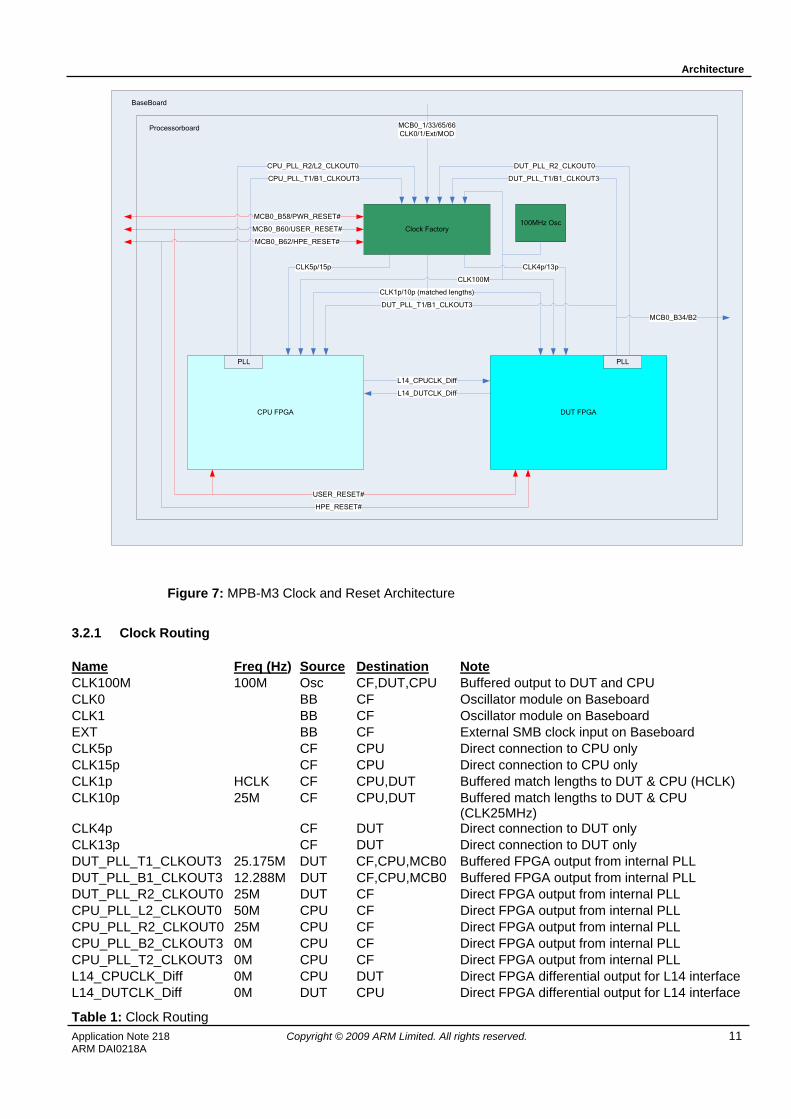
3.2 Clock architecture The clock factory is a Gleichmann specific implementation and is treated as a blackbox with configuration performed by their software application [2] and the Altera Quartus II tools. Figure 7 shows the clock and reset architecture for the system.
Architecture
Application Note 218 Copyright © 2009 ARM Limited. All rights reserved. 11 ARM DAI0218A
BaseBoard
Processorboard
DUT FPGACPU FPGA
Clock Factory
CLK1p/10p (matched lengths)
100MHz Osc
CLK100M
DUT_PLL_T1/B1_CLKOUT3
CPU_PLL_R2/L2_CLKOUT0 DUT_PLL_R2_CLKOUT0
CPU_PLL_T1/B1_CLKOUT3
CLK5p/15p CLK4p/13p
PLLPLL
DUT_PLL_T1/B1_CLKOUT3
MCB0_B34/B2
MCB0_1/33/65/66CLK0/1/Ext/MOD
L14_CPUCLK_Diff
L14_DUTCLK_Diff
MCB0_B58/PWR_RESET#
MCB0_B60/USER_RESET#
MCB0_B62/HPE_RESET#
USER_RESET#
HPE_RESET#
Figure 7: MPB-M3 Clock and Reset Architecture
3.2.1 Clock Routing Name Freq (Hz) Source Destination Note CLK100M 100M Osc CF,DUT,CPU Buffered output to DUT and CPU CLK0 BB CF Oscillator module on Baseboard CLK1 BB CF Oscillator module on Baseboard EXT BB CF External SMB clock input on Baseboard CLK5p CF CPU Direct connection to CPU only CLK15p CF CPU Direct connection to CPU only CLK1p HCLK CF CPU,DUT Buffered match lengths to DUT & CPU (HCLK) CLK10p 25M CF CPU,DUT Buffered match lengths to DUT & CPU
(CLK25MHz) CLK4p CF DUT Direct connection to DUT only CLK13p CF DUT Direct connection to DUT only DUT_PLL_T1_CLKOUT3 25.175M DUT CF,CPU,MCB0 Buffered FPGA output from internal PLL DUT_PLL_B1_CLKOUT3 12.288M DUT CF,CPU,MCB0 Buffered FPGA output from internal PLL DUT_PLL_R2_CLKOUT0 25M DUT CF Direct FPGA output from internal PLL CPU_PLL_L2_CLKOUT0 50M CPU CF Direct FPGA output from internal PLL CPU_PLL_R2_CLKOUT0 25M CPU CF Direct FPGA output from internal PLL CPU_PLL_B2_CLKOUT3 0M CPU CF Direct FPGA output from internal PLL CPU_PLL_T2_CLKOUT3 0M CPU CF Direct FPGA output from internal PLL L14_CPUCLK_Diff 0M CPU DUT Direct FPGA differential output for L14 interface L14_DUTCLK_Diff 0M DUT CPU Direct FPGA differential output for L14 interface
Table 1: Clock Routing
Architecture
12 Copyright © 2009 ARM Limited. All rights reserved. Application Note 218 ARM DAI0218A
3.2.2 Reset Routing
Name Source Destination Note PWR_RESET# BB CF O/D output from supply monitor (internal use) USER_RESET# All CF,CPU,DUT Push button on Processor board O/D HPE_RESET# CF BB, DUT Driven by USER_RESET# and PWR_RESET#
Table 2: Reset Routing
Notes:
BB: BaseBoard
CF: Clock Factory
CPU: CPU FPGA
DUT: DUT FPGA
OSC: Crystal Oscillator module.
The System only uses the USER_RESET# signal and this drives all internal resets (nPOR, nHRESET etc). The design ignores PWR_RESET# and HPE_RESET#.
The CPU FPGA drives the nHRESET signal between the CPU and DUT FPGA to create a synchronous reset (with respect to HCLK) in the DUT FPGA. The DUT FPGA uses this to resynchronise resets to all other clock domains within the FPGA.
3.2.3 Clock and Reset Destinations
Device Clock Freq Clock ref Reset ref Note CPU HCLK CLK1p HRESETn AHB/APB infrastructure HCLK CLK1p HRESETn Runs as CPU frequency SMC (ZBT & NOR) HCLK CLK1p HRESETn CPU FPGA memory controllers and I/F to USB IC UART 25MHz CLK10p HRESETn PL011 SPI 25MHz CLK10p HRESETn PL022 I2C HCLK CLK1p HRESETn DS702 VIDEO 23.75MHz CLK4p HRESETn Video/LCD controller pixel clock AC97 12.288MHz CLK13p HRESETn PL041 SD/MMC 25MHz CLK10p HRESETn PL181 Character LCD HCLK CLK1p HRESETn DS700 7SEG Display HCLK CLK1p HRESETn TBD Timer 1MHz CLK10p HRESETn SP804 Real Time Clock 1Hz CLK10p HRESETn PL031 Watch Dog 1Hz CLK10p HRESETn SP805 USB HCLK CLK1p HRESETn External IC ISP1761 Static Memory HCLK CLK1p HRESETn Memory controller on DUT FPGA
Table 3: Clock and Reset Destinations
All the peripherals that have an AHB or APB interface have that interface running at CLK1p.
CLK100M is used to derive all peripheral clocks where appropriate since this is a non variable clock and ideal for timers, watchdogs etc.
The Reset column refers to the reset signal that is re-synchronised to the respective clock domain.
Architecture
Application Note 218 Copyright © 2009 ARM Limited. All rights reserved. 13 ARM DAI0218A
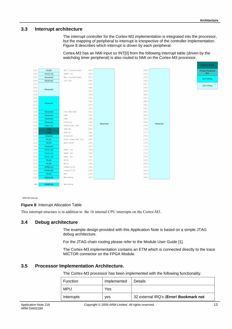
3.3 Interrupt architecture The interrupt controller for the Cortex-M3 implementation is integrated into the processor, but the mapping of peripheral to interrupt is irrespective of the controller implementation. Figure 8 describes which interrupt is driven by each peripheral.
Cortex-M3 has an NMI input so INT[0] from the following interrupt table (driven by the watchdog timer peripheral) is also routed to NMI on the Cortex-M3 processor.
Ethernet
USB
PL111
PL181
PL041
PL031
Reserved
PL011 (3)
SP805 (0)
SP804 (0)
SP804 (1)
[32]WatchDog
Timer[1:0]
[33]
[34]
[35]Timer[3:2]
[37]
[36]
[38]
Reserved
Reserved
Flexray
CAN
LIN
[39]
[40]
[41]
[42]
RTC
[43]
[44]
UART (3)
PL011 (1)
[45]
UART (1)
[46]
[47]
MCIa
MCIb
[48]
[49]
[50]
PL181
AACI/AC97
[51]
[52]
[53]
CLCD combined Int
[54]
[55]
[56]
[57]
Ethernet
USB DC
[58]
[59]
[60]
[61]
[62]
[63] [95]
[64]
Reserved
[65]
[66]
[67]
[68]
[69]
[70]
[71]
[72]
[73]
[74]
[75]
[76]
[77]
[78]
[79]
[80]
[81]
[82]
[83]
[84]
MPB-M3 Interrupt
[00]
[01]
[02]
[03]
[04]
[05]
[06]
[07]
[08]
[09]
[10]
[11]
[12]
[13]
[14]
[15]
[16]
[31]
Reserved
[17]
[18]
[19]
[20]
[21]
[22]
[23]
[24]
[25]
[26]
[27]
[28]
[29]
[30]
[85]
[86]
[87]
[88]
[89]
[90]
[91]
[92]
[93]
[94]
Reserved
Reserved
Reserved
I2C ADC/DAC
SPI touchscreenPL022 Private Peripheral Bus
DUT FPGA
External Device
Char LCD Character LCD
Reserved
CPU FPGA
I2C DVI
Reserved Ext touchscreen
USB HCUSB
PL011 (2) UART (2)
PL011 (0) UART (0)
Reserved
SP805 (0) WatchDogNMI
Figure 8: Interrupt Allocation Table
This interrupt structure is in addition to the 16 internal CPU interrupts on the Cortex-M3.
3.4 Debug architecture The example design provided with this Application Note is based on a simple JTAG debug architecture.
For the JTAG chain routing please refer to the Module User Guide [1].
The Cortex-M3 implementation contains an ETM which is connected directly to the trace MICTOR connector on the FPGA Module.
3.5 Processor Implementation Architecture. The Cortex-M3 processor has been implemented with the following functionality.
Function Implemented Details
MPU Yes
Interrupts yes 32 external IRQ’s (Error! Bookmark not
Architecture
14 Copyright © 2009 ARM Limited. All rights reserved. Application Note 218 ARM DAI0218A
defined.)
Priority Yes 3 bits 8 levels
Trace yes Full debug including data matching
JTAG & SWD Yes Both JTAG and Single wire debug present
Clock gating No No architectural clock gating implemented in design
All registers reset No Not all registers are reset after system reset
Internal observability No No internal observability implemented
WIC No No WIC implemented
SYSTICK Yes 100kHz reference clock implemented with divider to 10ms.
Power Management No The Sleep modes do not perform any clock stopping, but will allow the WFI type functionality.
Multiprocessor Communication
No No support for multiprocessor communication is implemented.
Table 4: Cortex-M3 Configuration
Hardware description
Application Note 218 Copyright © 2009 ARM Limited. All rights reserved. 15 ARM DAI0218A
4 Hardware description
4.1 Top Level The top level of the DUT FGPA is fpga_dut.v
This top level:
• Handles all the static tie offs,
• Maps the internal design signals to the board connections,
• Includes/calls the header file which contains the configuration information for the example system.
• Instances any special IO cells the design requires (e.g., the DDR registers for the Video connections).
The top level module instantiates the dut_logic,v module which in turn instances all the blocks in the example system and defines the interconnect between them.
4.1.1 Configuring the Example System
As an example of how to prototype a system too large for the Customer System FPGA, the definitions file (fpga_dut_defs.v) contains four defines which allow the system to be built without significant portions of the design to reduce size or improve performance.
By default, the audio codec and MMC/SD card interfaces are included but by un-commenting or commenting out the following lines, the system configuration can be altered.
Define Effect `define INCLUDE_CLCD This includes the Colour LCD and Video controller block (user supplied). Without this
define, the pixel clock is not driven and the data and control lines are tied to ‘0’. Which means that the video bus will not drive any data or clock at all.
`define VGA Implement the VGA Pattern Generator 640x480 if no CLCD present `define SVGA Implement the VGA Pattern Generator 800x600 if no CLCD present `define XVGA Implement the VGA Pattern Generator 1024x768 if no CLCD present `define INCLUDE_AACI This includes the Primecell PL041 (Audio Codec interface). `define INCLUDE_MCI This includes the Primecell PL181 (MMC/SD interface). `define INCLUDE_DMC This includes the DDR memory interface (user supplied).
If these components are not included then the video and LCD controller does not have any route to memory so the address out of the video and LCD controller block is connected to the read data bus giving a static image on any screen attached to that interface.
Table 5: System Configuration
Programmer’s model
16 Copyright © 2009 ARM Limited. All rights reserved. Application Note 218 ARM DAI0218A
5 Programmer’s model
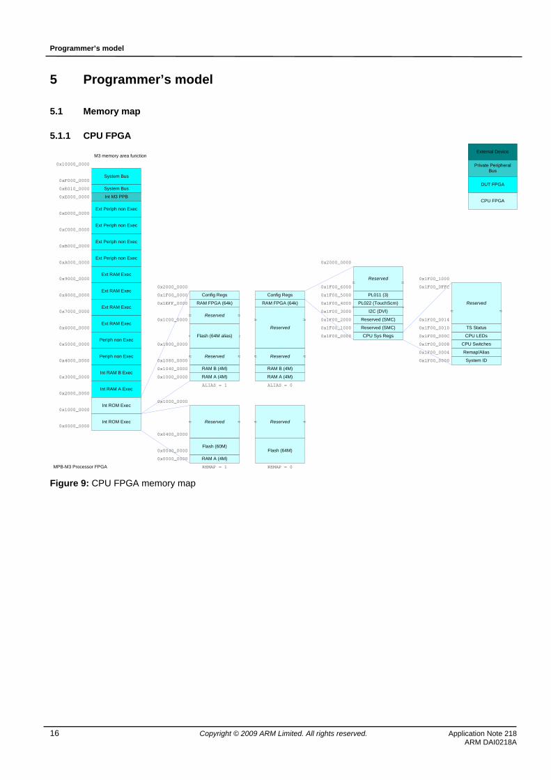
5.1 Memory map
5.1.1 CPU FPGA
Reserved
ReservedInt ROM Exec
Int RAM A Exec
Int RAM B Exec
Int M3 PPB
0x0000_0000
0x1000_0000
0x2000_0000
0x3000_0000
0x4000_0000
0x5000_0000
0x6000_0000
0x7000_0000
0x8000_0000
0x9000_0000
0xA000_0000
0xB000_0000
0xC000_0000
0xD000_0000
0xE000_0000
0xF000_0000
CPU Sys Regs0x1F00_0000
0x1F00_1000
0x0400_0000
0x0000_0000
Flash (64M)
0x1000_0000
Reserved
≈≈
≈≈
0x2000_0000Ext Periph non Exec
Ext RAM Exec
Ext RAM Exec
MPB-M3 Processor FPGA
Ext RAM Exec
Ext RAM Exec
Periph non Exec
Int ROM Exec
Periph non Exec
RAM A (4M)
Flash (60M)
Reserved ≈≈
0x0040_0000
REMAP = 1 REMAP = 0
RAM A (4M)
RAM B (4M)0x1040_0000
0x1080_0000
0x1000_0000
0x1800_0000
Flash (64M alias)
0x1C00_0000Reserved
Config Regs0x1F00_0000
0x2000_0000
≈≈
RAM A (4M)
RAM B (4M)
Config Regs
ALIAS = 1 ALIAS = 0
≈≈
Reserved (SMC)
Reserved (SMC)0x1F00_2000
0x1F00_3000
M3 memory area function
Reserved
RAM FPGA (64k)
≈≈
≈≈Reserved
RAM FPGA (64k)
≈≈
0x1EFF_0000
Ext Periph non Exec
Ext Periph non Exec
Ext Periph non Exec
0xE010_0000
System Bus
0x10000_0000
System Bus
CPU LEDs
CPU Switches
Remap/Alias
0x1F00_0000
0x1F00_0004
0x1F00_0008
0x1F00_000C
Reserved
0x1F00_1000
0x1F00_0FFC
PL022 (TouchScrn)0x1F00_4000
0x1F00_5000
≈≈
≈≈
Private Peripheral Bus
DUT FPGA
External Device
CPU FPGA
System ID
0x1F00_0010
0x1F00_6000
I2C (DVI)
TS Status
0x1F00_0014
PL011 (3)
Figure 9: CPU FPGA memory map
Programmer’s model
Application Note 218 Copyright © 2009 ARM Limited. All rights reserved. 17 ARM DAI0218A
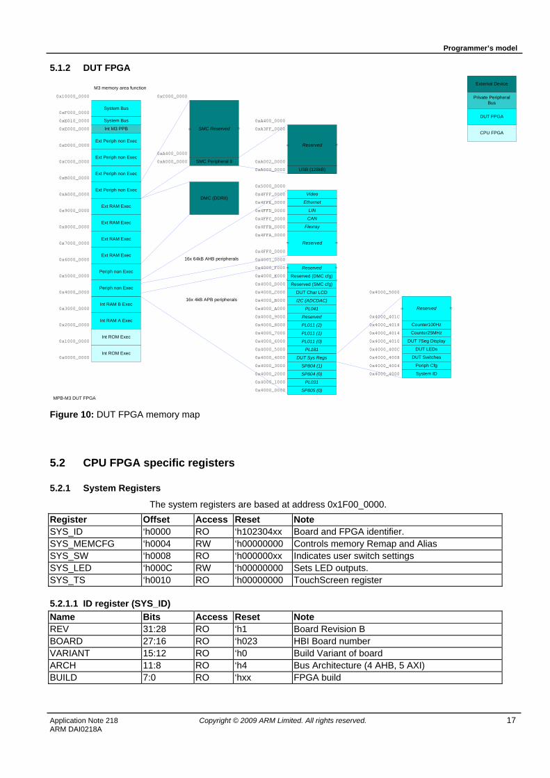
5.1.2 DUT FPGA
SMC Reserved
Int ROM Exec
Int RAM A Exec
Int RAM B Exec
Int M3 PPB
0x0000_0000
0x1000_0000
0x2000_0000
0x3000_0000
0x4000_0000
0x5000_0000
0x6000_0000
0x7000_0000
0x8000_0000
0x9000_0000
0xA000_0000
0xB000_0000
0xC000_0000
0xD000_0000
0xE000_0000
0xF000_0000
Ext Periph non Exec
Ext RAM Exec
Ext RAM Exec
MPB-M3 DUT FPGA
Ext RAM Exec
Ext RAM Exec
Periph non Exec
Int ROM Exec
Periph non Exec
M3 memory area function
DUT LEDs
Ext Periph non Exec
Ext Periph non Exec
Ext Periph non Exec
0xE010_0000
System Bus
0x10000_0000
System Bus
DMC (DDRII)Ethernet
Video
PL041
PL031
I2C (ADCDAC)
Reserved
SP805 (0)
SP804 (0)
SP804 (1)
PL011 (1)
PL181
Reserved
0x4000_0000
0x4000_1000
0x4000_2000
0x4000_3000
0x4000_4000
0x4000_5000
0x4000_6000
0x4000_7000
0x4000_8000
0x4000_9000
0x4000_A000
0x4000_D000≈≈
DUT Sys Regs
LIN
CAN
Flexray
Reserved
0x4001_0000
0x4FF0_0000
0x4FFF_0000
0x4FFE_0000
0x4FFD_0000
0x4FFC_0000
0x4FFB_0000
0x4FFA_0000
0x5000_0000
≈≈
16x 4kB APB peripherals
16x 64kB AHB peripherals
SMC Peripheral 00xA000_0000
0xA400_0000
0xC000_0000
USB (128kB)
Reserved
0xA000_0000
0xA400_0000
0xA002_0000
0xA3FF_0000
≈≈
DUT Switches
DUT Char LCD
0x4000_B000
DUT 7Seg Display
0x4000_4000
0x4000_4004
0x4000_4008
0x4000_400C
0x4000_4010
Reserved
0x4000_5000
Reserved (SMC cfg)
Reserved (DMC cfg)
≈≈
0x4000_C000
Private Peripheral Bus
DUT FPGA
External Device
CPU FPGA
PL011 (2)
PL011 (0)
0x4000_E000
0x4000_F000 ≈≈
≈≈
Counter25MHz
Counter100Hz
0x4000_4014
Periph Cfg
System ID
0x4000_4018
0x4000_401C
Figure 10: DUT FPGA memory map
5.2 CPU FPGA specific registers
5.2.1 System Registers
The system registers are based at address 0x1F00_0000. Register Offset Access Reset Note SYS_ID ‘h0000 RO ‘h102304xx Board and FPGA identifier. SYS_MEMCFG ‘h0004 RW ‘h00000000 Controls memory Remap and Alias SYS_SW ‘h0008 RO ‘h000000xx Indicates user switch settings SYS_LED ‘h000C RW ‘h00000000 Sets LED outputs. SYS_TS ‘h0010 RO ‘h00000000 TouchScreen register
5.2.1.1 ID register (SYS_ID) Name Bits Access Reset Note REV 31:28 RO ‘h1 Board Revision B BOARD 27:16 RO ‘h023 HBI Board number VARIANT 15:12 RO ‘h0 Build Variant of board ARCH 11:8 RO ‘h4 Bus Architecture (4 AHB, 5 AXI) BUILD 7:0 RO ‘hxx FPGA build
Programmer’s model
18 Copyright © 2009 ARM Limited. All rights reserved. Application Note 218 ARM DAI0218A
5.2.1.2 Memory Configuration (SYS_MEMCFG) Name Bits Access Power On
Reset Note
Reserved 31:3 SWDPEN 2 RW ‘b0 Single Wire Debug Port Enable. 1 is SWD 0
JTAG. Not used in Cortex-M3 implementation as this autodetects serial or JTAG.
ALIAS 1 RW ‘b1 Alias FLASH. 1 is Aliased on 0 Aliased off REMAP 0 RW ‘b0 Remap SSRAM. 1 is Remap on 0 Remap off
Default memory mapping is Flash Aliased and SSRAM not remapped. The register is reset at power on to this state, but any debug reset or system reset will not change the values stored. This allows the SRAM to be programmed placed and address 0x0000_0000 and execute after generating a system reset.
5.2.1.3 Switches (SYS_SW) Name Bits Access Reset Note Reserved 31:8 USER_SWITCH 7:0 RO ‘h-- Always returns value of user switches
5.2.1.4 LEDs (SYS_LED) Name Bits Access Reset Note Reserved 31:8 LED 7:0 RW ‘h00 Returns value in register. 1 is LED on 0 LED off
5.2.1.5 TouchScreen (SYS_TS) Name Bits Access Reset Note Reserved 31:2 TS_INT 1 RO ‘b- External Interrupt from Touchscreen TS_BUSY 0 RO ‘b- External Busy signal from Touchscreen
5.2.2 Video (I2C for DVI)
The DS702 peripheral is used for the interface and implements a bit banging method for the I2C interface. The base address for this interface is 0x1F00_3000.
Register Offset Access Reset Note SB_CONTROL ‘h0000 R ‘b0- Status Register of I/O signals SB_CONTROLS ‘h0000 W ‘b00 Set Output bits SB_CONTROLC ‘h0004 WO ‘b00 Clear Output bits
5.2.2.1 SB Status register (SB_CONTROL) Name Bits Access Reset Note Reserved 31:2 SB_SDA 1 RO ‘b0 Level of SDA signal SB_SCL 0 RO ‘b0 Level of SCL signal
5.2.2.2 SB Set register (SB_CONTROLS) Name Bits Access Reset Note Reserved 31:2 SB_nSDAOUTEN 1 W ‘b0 Sets SDA line when 1 SB_SCLOUT 0 W ‘b0 Sets SCL line when 1
5.2.2.3 SB Clear register (SB_CONTROLC) Name Bits Access Reset Note Reserved 31:2
Programmer’s model
Application Note 218 Copyright © 2009 ARM Limited. All rights reserved. 19 ARM DAI0218A
SB_nSDAOUTEN 1 W ‘b0 Clears SDA line when 1 SB_SCLOUT 0 W ‘b0 Clears SCL line when 1
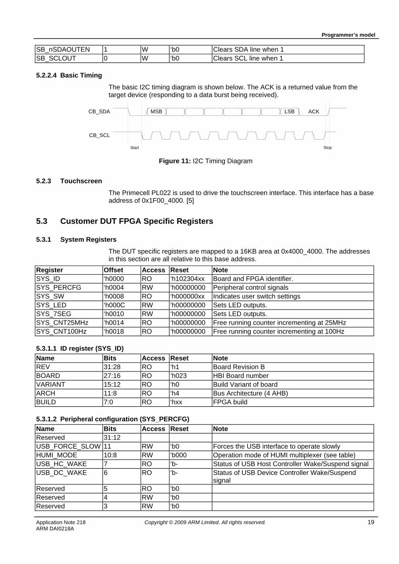
5.2.2.4 Basic Timing
The basic I2C timing diagram is shown below. The ACK is a returned value from the target device (responding to a data burst being received).
MSB LSBCB_SDA
CB_SCL
ACK
StopStart Figure 11: I2C Timing Diagram
5.2.3 Touchscreen
The Primecell PL022 is used to drive the touchscreen interface. This interface has a base address of 0x1F00_4000. [5]
5.3 Customer DUT FPGA Specific Registers
5.3.1 System Registers
The DUT specific registers are mapped to a 16KB area at 0x4000_4000. The addresses in this section are all relative to this base address.
Register Offset Access Reset Note SYS_ID ‘h0000 RO ‘h102304xx Board and FPGA identifier. SYS_PERCFG ‘h0004 RW ‘h00000000 Peripheral control signals SYS_SW ‘h0008 RO ‘h000000xx Indicates user switch settings SYS_LED ‘h000C RW ‘h00000000 Sets LED outputs. SYS_7SEG ‘h0010 RW ‘h00000000 Sets LED outputs. SYS_CNT25MHz ‘h0014 RO ‘h00000000 Free running counter incrementing at 25MHz SYS_CNT100Hz ‘h0018 RO ‘h00000000 Free running counter incrementing at 100Hz
5.3.1.1 ID register (SYS_ID) Name Bits Access Reset Note REV 31:28 RO ‘h1 Board Revision B BOARD 27:16 RO ‘h023 HBI Board number VARIANT 15:12 RO ‘h0 Build Variant of board ARCH 11:8 RO ‘h4 Bus Architecture (4 AHB) BUILD 7:0 RO ‘hxx FPGA build
5.3.1.2 Peripheral configuration (SYS_PERCFG) Name Bits Access Reset Note Reserved 31:12 USB_FORCE_SLOW 11 RW ‘b0 Forces the USB interface to operate slowly HUMI_MODE 10:8 RW ‘b000 Operation mode of HUMI multiplexer (see table) USB_HC_WAKE 7 RO ‘b- Status of USB Host Controller Wake/Suspend signal USB_DC_WAKE 6 RO ‘b- Status of USB Device Controller Wake/Suspend
signal Reserved 5 RO ‘b0 Reserved 4 RW ‘b0 Reserved 3 RW ‘b0
Programmer’s model
20 Copyright © 2009 ARM Limited. All rights reserved. Application Note 218 ARM DAI0218A
Reserved 2 RO ‘b0 WPROT 1 RO ‘b0 Status of MCI WPROT bit, 1 write protected CARDIN 0 RO ‘b0 Status of MCI card Present, 1 card inserted
The HUMI Mode bits define how the scheduler selects the different display components on the system. This can be used for system debug.
Mode Bit value Note Scheduler 000 Round robin schedule to all HUMI devices LEDs 001 HUMI LEDs only output 7Segment 0 010 HUMI 7Segment display 0 only output 7Segment 1 011 HUMI 7Segment display 1 only output 7Segment 2 100 HUMI 7Segment display 2 only output 7Segment 3 101 HUMI 7Segment display 3 only output Character LCD 110 HUMI character LCD only output Reserved 111 Reserved - Do Not Use
5.3.1.3 Switches (SYS_SW) Name Bits Access Reset Note Reserved 31:8 USER_BUT[3:0] 7:4 RO ‘h- Always returns value of user buttons USER_SW[3:0] 3:0 RO ‘h- Always returns value of user switches
5.3.1.4 LED’s (SYS_LED) Name Bits Access Reset Note Reserved 31:8 LED 7:0 RW ‘h00 Returns value in register. 1 is LED on 0 LED off
5.3.1.5
Programmer’s model
Application Note 218 Copyright © 2009 ARM Limited. All rights reserved. 21 ARM DAI0218A
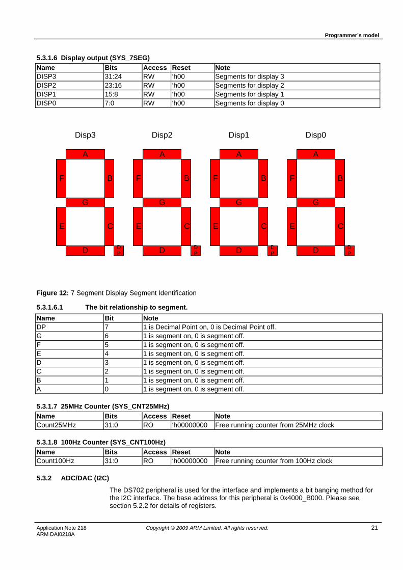
5.3.1.6 Display output (SYS_7SEG) Name Bits Access Reset Note DISP3 31:24 RW ‘h00 Segments for display 3 DISP2 23:16 RW ‘h00 Segments for display 2 DISP1 15:8 RW ‘h00 Segments for display 1 DISP0 7:0 RW ‘h00 Segments for display 0
A
G
D
B
DP
CE
F
A
G
D
B
DP
CE
F
A
G
D
B
DP
CE
F
A
G
D
B
DP
CE
F
Disp3 Disp2 Disp1 Disp0
Figure 12: 7 Segment Display Segment Identification
5.3.1.6.1 The bit relationship to segment. Name Bit Note DP 7 1 is Decimal Point on, 0 is Decimal Point off. G 6 1 is segment on, 0 is segment off. F 5 1 is segment on, 0 is segment off. E 4 1 is segment on, 0 is segment off. D 3 1 is segment on, 0 is segment off. C 2 1 is segment on, 0 is segment off. B 1 1 is segment on, 0 is segment off. A 0 1 is segment on, 0 is segment off.
5.3.1.7 25MHz Counter (SYS_CNT25MHz) Name Bits Access Reset Note Count25MHz 31:0 RO ‘h00000000 Free running counter from 25MHz clock
5.3.1.8 100Hz Counter (SYS_CNT100Hz) Name Bits Access Reset Note Count100Hz 31:0 RO ‘h00000000 Free running counter from 100Hz clock
5.3.2 ADC/DAC (I2C)
The DS702 peripheral is used for the interface and implements a bit banging method for the I2C interface. The base address for this peripheral is 0x4000_B000. Please see section 5.2.2 for details of registers.
Programmer’s model
22 Copyright © 2009 ARM Limited. All rights reserved. Application Note 218 ARM DAI0218A
5.3.3 Character LCD
The Character display component is the DS700 and interfaces to the industry standard Hitachi HD44780 controller. It uses 11 signals 8 data, 1 strobe (E), read/write (RnW) and Register/data select (RS).
Note: the interface can be a 4-bit or 8-bit interface. For this application it is in 8-bit mode.
Note: When the display is used with a 4-bit interface an 8-bit value has to be written/read as two consecutive nibbles, writing/reading bits [7:4] first into register bits [7:4], then writing/reading bits [3:0] into register bits [7:4].
Register Offset Access Reset Note CHAR_COM ‘h0000 RW ‘h00000000 A write will write to the display controller command
register. A read will initiate a status register access (returns value later in CHAR-RD).
CHAR_DAT ‘h0004 RW ‘h00000000 A write will write to the display controller data register. A read will initiate a data register access (returns value later in CHAR-RD).
CHAR_RD ‘h0008 RO ‘h00000000 Contains data from last CHAR_COM or CHAR_DAT read when CHAR_RAW[8] is set.
CHAR_RAW ‘h000C RW ‘h00000000 Reading bit 8 indicates if access is complete. Writing 0 to bit 8 clears bit.
CHAR_MASK ‘h0010 RW ‘h00000000 Set bit 0 to 1 will generate interrupt when access completes.
CHAR_STAT ‘h0014 RO ‘h00000000 Returns status of Access Complete ANDed with CHAR MASK.
Programmer’s model
Application Note 218 Copyright © 2009 ARM Limited. All rights reserved. 23 ARM DAI0218A
5.3.3.1 Character Command Register (CHAR_COM)
Name Bits Access Reset Note Reserved 31:8 RW ‘h00000000 COMMAND 7:0 RW ‘h00000000 A write will write to the display controller command
register. A read will initiate a status register access (returns value later in CHAR_RAW and CHAR-RD).
5.3.3.2 Character Data Register (CHAR_DAT)
Name Bits Access Reset Note Reserved 31:8 RW ‘h00000000 DATA 7:0 RW ‘h00000000 A write will write to the display controller data
register. A read will initiate a data register access (returns value later in CHAR_RAW and CHAR-RD
5.3.3.3 Character RD Register (CHAR_RD)
Name Bits Access Reset Note Reserved 31:8 RO ‘h00000000 READ 7:0 RO ‘h00000000 Contains data from last CHAR_COM or
CHAR_DAT read when DONE is set.
5.3.3.4 Character Command Register (CHAR_RAW)
Name Bits Access Reset Note Reserved 31:9 RW ‘h0000000 DONE 8 RW ‘b0 Reading indicates if access is complete. Writing 0
clears bit. Reserved 7:0 RW ‘h00
Note: If a transaction is attempted before DONE is asserted (CHAR_RAW register) by the controller then it maybe ignored and the command/data transfer could be lost. Once DONE is asserted it can be cleared and a transaction started.
5.3.3.5 Character Interrupt Mask Register (CHAR_MASK)
Name Bits Access Reset Note Reserved 31:1 RW ‘h00000000 MASKINT 0 RW ‘b0 Set to 1 will generate interrupt when access
completes (CHAR_DONE set)
5.3.3.6 Character Status Register (CHAR_STAT)
Name Bits Access Reset Note Reserved 31:1 RW ‘h00000000
Programmer’s model
24 Copyright © 2009 ARM Limited. All rights reserved. Application Note 218 ARM DAI0218A
STATINT 0 RW ‘b0 Returns status of CHAR_DONE ANDed with CHAR_MASKINT.
5.3.4 Video
This is a user supplied component with basic interfaces brought into the DUT FPGA to enable implementation.
The DVI-I controller device [7] includes an I2C (DS702) serial bus for configuration this is implemented in the CPU FPGA (see section 5.2.2 for details of registers). The Datasheet [7] covers the data format and process for configuration.
The example clock source for the video pixel clock is derived from the PLL in the DUT FPGA and drives a clock input of the DUT FPGA (CLK4p) via the clock factory. The clock source isset by the HPE_Desk application on the PC and the frequency is determined by the PLL implemented in the DUT FPGA.
Note: though the interface to the Video and LCD displays is driven by the processor FPGA, the peripheral is in the Customer DUT FPGA and the video/LCD signals are driven across the interconnect between the two FPGAs (see section 10.1).
The signals from the CLCD are mapped to the video signals as follows. PL111 [6] Name LCD name Video Name Note CLCP LCD_R_SHFCLK VIDEOCLK Pixel Clock CLPOWER - - Not Used CLLP LCD_R_HSYNC VIDEOHSYNC Horizontal Sync CLFP LCD_R_VSYNC VIDEOVSYNC Vertical Sync CLAC LCD_R_M_DE VIDEODE Data Enable CLLE - - Not Used CLD[19:16] - VIDEO[11:8] Green Data DDR encoded rising edge CLD[15:8] - VIDEO[7:0] Blue Data DDR encoded rising edge CLD[7:0] - VIDEO[11:4] Red Data DDR encoded falling edge CLD[23:20] - VIDEO[3:0] Green Data DDR encoded falling edge CLD[23:0] - VIDEO[11:0] RGB colour Data DDR encoded falling edge CLD[7:2] LCD_TTL_R[5:0] - Red Data MSB’s CLD[15:10] LCD_TTL_G[5:0] - Green Data MSB’s CLD[23:18] LCD_TTL_B[5:0] - Blue Data MSB’s
- - VIDEORESET# Reset synchronised to pixel clock - - VIDEOHPINT Hot Plug interrupt (Not Used) - - VIDEOMODE Video Mode GPIO pin of video chip (Not Used) - - VIDEO_I2C_SC
L Video Chip configuration bus
- - VIDEO_I2C_SDA
Video Chip configuration bus
- LCD_BLON - Back Light On (output tied to 1) - LCD_VDON - LCD Power On (output tied to 1)
Table 6: Video and LCD Connections
For further data on the video encoding see the Datasheet for Chrontel CH7303A device [7].
5.3.5 Timer
The SP804 ADK component is used for the timers. See the TRM for details about its functionality [8]. The Timer clock is set at 1MHz and is derived from the 100MHz clock.
The combined interrupt is used so each SP804 implementation only has 1 interrupt output (see section 3.3).
Programmer’s model
Application Note 218 Copyright © 2009 ARM Limited. All rights reserved. 25 ARM DAI0218A
5.3.6 RTC
The PL031 PrimeCell is used as the RTC. See the TRM for details about its functionality[9]. The RTC clock is feed from the RTCCLK signal and is 1Hz and is derived from the 100MHz clock.
5.3.7 WatchDog
The SP805 ADK component is used for the watchdog. See the TRM for details about its functionality[10]. The clock is set at 1Hz and is derived from the 100MHz clock.
5.3.8 Dynamic Memory Controller
This is a user supplied component with basic interfaces brought into the DUT FPGA to enable implementation.
5.3.9 Static Memory Controller
The Static memory interface implemented in the design is specifically to allow communication to the ISP1761 USB device [14]. Configuration and use of this is outside the scope of this Application Note
5.3.10 UARTs
The PL011 PrimeCell is used as the UART. See the TRM for details about its functionality [11].
The clock source is divided down and is derived from the 100MHz clock.
5.3.11 Audio (AACI/AC97)
The PL041 PrimeCell is used as the AACI. See the TRM for details about its functionality [12]. The AACI is a modification of the PrimeCell with increased FIFO depth to help improve transfer performance in FPGA.
The clock source is derived from the baseboard and drives a clock input of the DUT FPGA (CLK13p). The FPGA can also drive the AC_EXT_CLK to set the clock, but this option is not implemented.
5.3.12 MMC/SD (MMCI)
The PL181 PrimeCell is used as the MMC/SD card controller. See the TRM for details about its functionality [13]. The MMCI uses the bits in the system registers to identify the write protection and card inserted status (see section 5.3.1 for details).
5.4 Boot operation This system should normally boot from the board NOR Flash (the default configuration switches in the up position). The NOR Flash is preprogrammed with the boot monitor.
The user can also program custom boot software in NOR Flash, but note that any software configurable devices such as the UARTs etc will not work until properly configured.
RTL
26 Copyright © 2009 ARM Limited. All rights reserved. Application Note 218 ARM DAI0218A
6 RTL All of the RTL for this design is provided as Verilog or precompiled netlists. Example files are provided to allow the system to be rebuilt with the Altera Quartus II tools. The readme files provided with the application note show the version of the tools used to build the design.
6.1 Directory structure
Figure 13: Top Level Directory Structure
The application note has several directories:
• docs: Contains related documents including this document
• fpga_cpu: Contains a precompiled encrypted image for the processor FPGA in the design which contains the processor and the local peripherals.
• fpga_dut: Contains the verilog RTL files which describe the structure and design of the example system.
• software: Example software and utilities specific to the application note
• peripherals : Contains the verilog RTL or precompiled images of the peripherals used in the fpga_dut design.
MPS
M3
docs
fpga_cpu
fpga_dut
software
peripherals
RTL
Application Note 218 Copyright © 2009 ARM Limited. All rights reserved. 27 ARM DAI0218A
6.2 The fpga_dut Directory
Figure 14: Directory Structure within fpgu_dut Directory
The fpga_dut directory contains the Verilog required for top-level of the example customer system. This is in the directory logical/verilog and includes:
• The top level of the system which contains the IO instantiations and clock/reset sources. This is also a wrapper for the main/top-level logic module. This block is called fpga_dut.v and is the module called from the synthesis scripts.
• The logic module (called dut_logic.v) which describes the structure of the top level logic and instances the AHB peripherals and the APB sub-system.
• The associated AHB and APB peripherals which are specific to the Customer DUT FPGA (e.g., an AHB decoder, an AHB to APB bridge, an AHB-Lite Slave-to-Master Multiplexer, etc.).
• The system registers and their default settings are in this directory.
• The main defines which control what parts of the system are included in the build.
Also within this directory is the script for building the bit-file to download to the FPGA. The synthesis script is in physical/mpb_dut/altera/scripts and produces a routed, placed design in the physical/mpb_dut/altera/netlist directory. See the HPE Desk manuals for downloading this image to the FPGA [2].
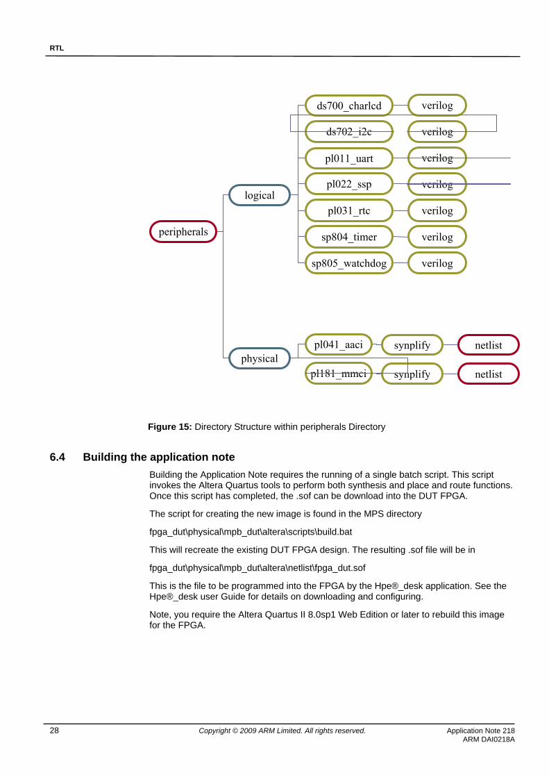
6.3 The peripherals Directory The peripherals directory contains verilog required for most of the ARM peripherals in the example customer system, with some blocks as pre built .vqm files (in /peripherals/physical /<peripheral_name>/synplify/netlist) to be read in by the build script. The function of each block is shown in section 3.
Each Primecell or other large IP block has its own directory (e.g. pl011_uart).
The netlists in these directories are pulled into the design by the scripts in the fpga_dut directory.
fpga_dut
logical
physical mpb_dut altera
verilog
scripts
netlist
RTL
28 Copyright © 2009 ARM Limited. All rights reserved. Application Note 218 ARM DAI0218A
Figure 15: Directory Structure within peripherals Directory
6.4 Building the application note Building the Application Note requires the running of a single batch script. This script invokes the Altera Quartus tools to perform both synthesis and place and route functions. Once this script has completed, the .sof can be download into the DUT FPGA.
The script for creating the new image is found in the MPS directory
fpga_dut\physical\mpb_dut\altera\scripts\build.bat
This will recreate the existing DUT FPGA design. The resulting .sof file will be in
fpga_dut\physical\mpb_dut\altera\netlist\fpga_dut.sof
This is the file to be programmed into the FPGA by the Hpe®_desk application. See the Hpe®_desk user Guide for details on downloading and configuring.
Note, you require the Altera Quartus II 8.0sp1 Web Edition or later to rebuild this image for the FPGA.
peripherals
logical
physical pl041_aaci synplify
ds700_charlcd
netlist
ds702_i2c
pl011_uart
pl022_ssp
pl031_rtc
sp805_watchdog
sp804_timer
verilog
verilog
verilog
verilog
verilog
verilog
verilog
pl181_mmci synplify netlist
Functional testing
Application Note 218 Copyright © 2009 ARM Limited. All rights reserved. 29 ARM DAI0218A
7 Functional testing
7.1 Self-test The selftest code allows the user to confirm the functionality of their Microcontroller Prototyping System, and provides a starting point for writing end code to make use of the MPB peripherals.
7.1.1 Functionality
Selftest is a piece of diagnostic code for testing the following peripherals: AACI, MMCI, USB, UARTs, character LCD, LEDs, switches, SRAM memory, RTC and system clocks/interrupts.
Selftest is designed to run on the Keil Software Development System that is delivered with the Microcontroller Prototyping System. The user can interact with the software operation via the debugger’s console window.
The user interface displays a menu and prompts the user on how to operate each test. For more information on exactly how each test is working, refer to the provided code source, and readme files.
7.1.2 Compilation notes
A MicroVision project file is shipped as part of the selftest suite. This project file can be used to rebuild the code with MicroVision. A makefile is also provided, so that automated builds can be run.
7.1.3 Description
The selftest directory contains a suite of register level software tests for testing each of the MPB peripherals. The code fragments used may also prove useful in developing demonstration code or OS driver ports.
The project and executable files for these tests can be found under the \selftest\build\Build_Keil directory. To complete the tests it is necessary to connect a number of loopback cables to the board (see note below).
After connecting the test harness and loading the program image into the debugger (selftest_mpb.axf) each of the MPB peripherals may be tested individually, or altogether using ‘Run all tests’. The tests perform register level and basic functional tests on the MPB hardware reporting any errors found.
The source code for the tests are brought together in a single project file \build\Build_Keil\selftest_mpb.Uv2.
The source code for each peripheral test is split into separate directories for example \apaaci\ contains apaaci.c and apaaci.h for testing the AACI peripheral. The \main\ folder contains main.c and common.c which provide the user menu and functions that are common to all peripheral tests.
Note: If the default install directory is not used, then the project will have to be rebuilt in order for the debugger to display the source code automatically.
7.1.4 Selftest test harness
The MPB test code requires three separate cable assemblies to be connected to the board for complete testing. Note these cables are not supplied with the MPB but details of their connections are given here.
Functional testing
30 Copyright © 2009 ARM Limited. All rights reserved. Application Note 218 ARM DAI0218A
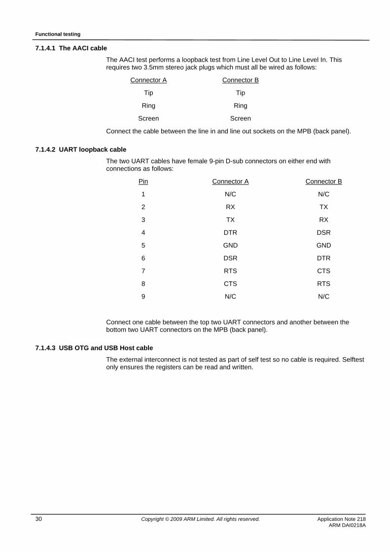
7.1.4.1 The AACI cable
The AACI test performs a loopback test from Line Level Out to Line Level In. This requires two 3.5mm stereo jack plugs which must all be wired as follows:
Connector A Connector B
Tip Tip
Ring Ring
Screen Screen
Connect the cable between the line in and line out sockets on the MPB (back panel).
7.1.4.2 UART loopback cable
The two UART cables have female 9-pin D-sub connectors on either end with connections as follows:
Pin Connector A Connector B
1 N/C N/C
2 RX TX
3 TX RX
4 DTR DSR
5 GND GND
6 DSR DTR
7 RTS CTS
8 CTS RTS
9 N/C N/C
Connect one cable between the top two UART connectors and another between the bottom two UART connectors on the MPB (back panel).
7.1.4.3 USB OTG and USB Host cable
The external interconnect is not tested as part of self test so no cable is required. Selftest only ensures the registers can be read and written.
Clock frequency settings
Application Note 218 Copyright © 2009 ARM Limited. All rights reserved. 31 ARM DAI0218A
8 Clock frequency settings Please see section 3.2 for the intended clock frequencies of the design.
Please use the online help of the HPE_Desk software for details on programming the clocks [2].
Example software
32 Copyright © 2009 ARM Limited. All rights reserved. Application Note 218 ARM DAI0218A
9 Example software The example software components of the firmware are:
• Platform Library – This handles the system initialization and retargets the C Library. To achieve this it provides a basic I/O subsystem that supports simple device drivers. Included with the platform library there is a simple terminal driver, UART, PS/2 keyboard and LCD drivers and support for semihosting I/O.
• Boot Monitor – This is the normal application that runs when the system is booted. It is built with the platform library and it is the platform library which handles the initial system initialization therefore any application that is built with the platform library (or handles it own initialization) could replace the boot monitor. It supports the following functions.
General file operations.
Programming images into flash.
Loading and running another application.
Board configuration.
• A semihost server that with handle standard ARM semihosting SWI’s.
• Flash Support – The code that is used by the boot monitor and NFU to program flash can be incorporated into a user application and is supplied in source form.
• MMC FAT support.
9.1 Boot Monitor User Interface The Boot Monitor command interpreter accepts user commands from the debugger console window or an attached terminal and carries out actions to complete the commands.
9.1.1 Boot Monitor Main Menu Commands
Command Format
Note
ALIAS <alias> <command string> Create an alias command <alias> for the string of commands in <command string>.
CD <directory path> Change directory to the one specified in <directory path>.
CLEAR BOOTSCRIPT Clear the current boot script. If no boot script is set then the boot monitor will always prompt for input no matter what the state of the 'run boot script' switch.
CONFIGURE Enter Configure Submenu
CONVERT BINARY <binary-file> LOAD_ADDRESS <address> [ENTRY_POINT <address>]
Adds information required by the RUN command to execute a binary file. The command will produce a file with the same name as the specified binary file but with the '.exe' file extension.
COPY <file1> <file2> Copies file <file1> to <file2>.
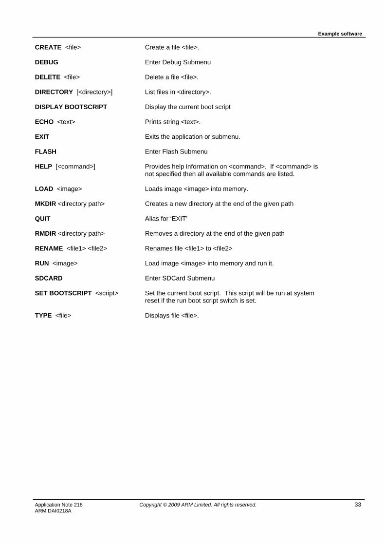
Example software
Application Note 218 Copyright © 2009 ARM Limited. All rights reserved. 33 ARM DAI0218A
CREATE <file> Create a file <file>.
DEBUG Enter Debug Submenu
DELETE <file> Delete a file <file>.
DIRECTORY [<directory>] List files in <directory>.
DISPLAY BOOTSCRIPT Display the current boot script
ECHO <text> Prints string <text>.
EXIT Exits the application or submenu.
FLASH Enter Flash Submenu
HELP [<command>] Provides help information on <command>. If <command> is not specified then all available commands are listed.
LOAD <image> Loads image <image> into memory.
MKDIR <directory path> Creates a new directory at the end of the given path
QUIT Alias for ‘EXIT’
RMDIR <directory path> Removes a directory at the end of the given path
RENAME <file1> <file2> Renames file <file1> to <file2>
RUN <image> Load image <image> into memory and run it.
SDCARD Enter SDCard Submenu
SET BOOTSCRIPT <script> Set the current boot script. This script will be run at system reset if the run boot script switch is set.
TYPE <file> Displays file <file>.
Example software
34 Copyright © 2009 ARM Limited. All rights reserved. Application Note 218 ARM DAI0218A
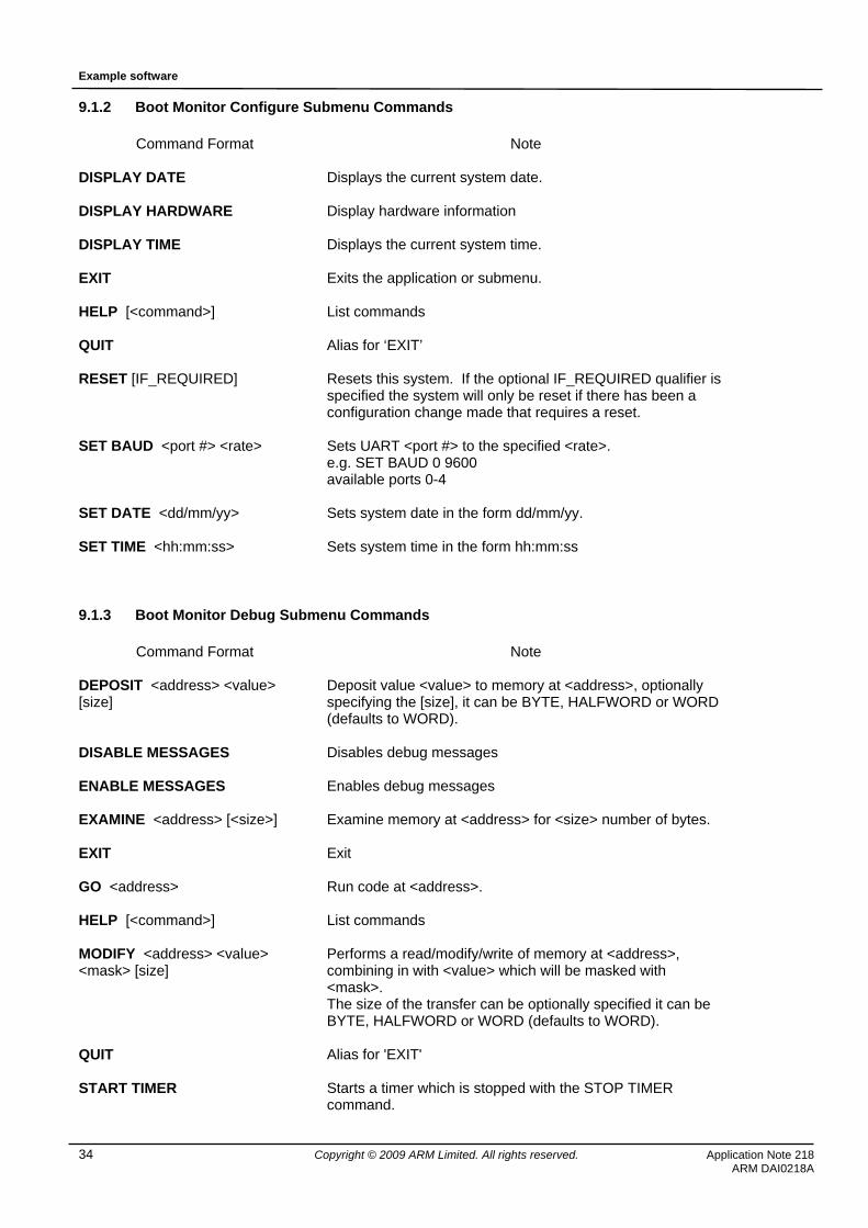
9.1.2 Boot Monitor Configure Submenu Commands
Command Format
Note
DISPLAY DATE
Displays the current system date.
DISPLAY HARDWARE
Display hardware information
DISPLAY TIME
Displays the current system time.
EXIT
Exits the application or submenu.
HELP [<command>]
List commands
QUIT
Alias for ‘EXIT’
RESET [IF_REQUIRED]
Resets this system. If the optional IF_REQUIRED qualifier is specified the system will only be reset if there has been a configuration change made that requires a reset.
SET BAUD <port #> <rate>
Sets UART <port #> to the specified <rate>. e.g. SET BAUD 0 9600 available ports 0-4
SET DATE <dd/mm/yy>
Sets system date in the form dd/mm/yy.
SET TIME <hh:mm:ss>
Sets system time in the form hh:mm:ss
9.1.3 Boot Monitor Debug Submenu Commands
Command Format
Note
DEPOSIT <address> <value> [size]
Deposit value <value> to memory at <address>, optionally specifying the [size], it can be BYTE, HALFWORD or WORD (defaults to WORD).
DISABLE MESSAGES
Disables debug messages
ENABLE MESSAGES
Enables debug messages
EXAMINE <address> [<size>]
Examine memory at <address> for <size> number of bytes.
EXIT
Exit
GO <address>
Run code at <address>.
HELP [<command>]
List commands
MODIFY <address> <value> <mask> [size]
Performs a read/modify/write of memory at <address>, combining in with <value> which will be masked with <mask>. The size of the transfer can be optionally specified it can be BYTE, HALFWORD or WORD (defaults to WORD).
QUIT
Alias for 'EXIT'
START TIMER
Starts a timer which is stopped with the STOP TIMER command.
Example software
Application Note 218 Copyright © 2009 ARM Limited. All rights reserved. 35 ARM DAI0218A
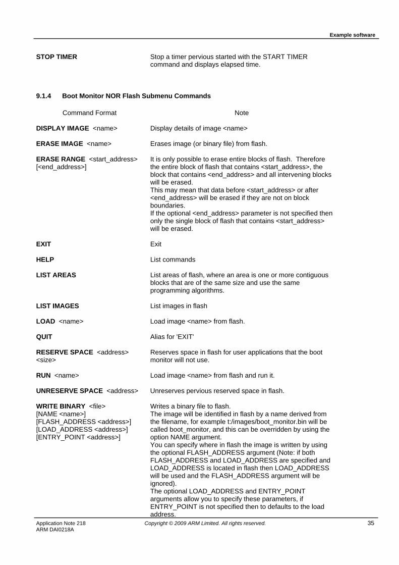
STOP TIMER
Stop a timer pervious started with the START TIMER command and displays elapsed time.
9.1.4 Boot Monitor NOR Flash Submenu Commands
Command Format
Note
DISPLAY IMAGE <name>
Display details of image <name>
ERASE IMAGE <name>
Erases image (or binary file) from flash.
ERASE RANGE <start_address> [<end_address>]
It is only possible to erase entire blocks of flash. Therefore the entire block of flash that contains <start_address>, the block that contains <end_address> and all intervening blocks will be erased. This may mean that data before <start_address> or after <end_address> will be erased if they are not on block boundaries. If the optional <end_address> parameter is not specified then only the single block of flash that contains <start_address> will be erased.
EXIT Exit
HELP List commands
LIST AREAS List areas of flash, where an area is one or more contiguous blocks that are of the same size and use the same programming algorithms.
LIST IMAGES List images in flash
LOAD <name> Load image <name> from flash.
QUIT Alias for 'EXIT'
RESERVE SPACE <address> <size>
Reserves space in flash for user applications that the boot monitor will not use.
RUN <name> Load image <name> from flash and run it.
UNRESERVE SPACE <address> Unreserves pervious reserved space in flash.
WRITE BINARY <file> [NAME <name>] [FLASH_ADDRESS <address>] [LOAD_ADDRESS <address>] [ENTRY_POINT <address>]
Writes a binary file to flash. The image will be identified in flash by a name derived from the filename, for example t:/images/boot_monitor.bin will be called boot_monitor, and this can be overridden by using the option NAME argument. You can specify where in flash the image is written by using the optional FLASH_ADDRESS argument (Note: if both FLASH_ADDRESS and LOAD_ADDRESS are specified and LOAD_ADDRESS is located in flash then LOAD_ADDRESS will be used and the FLASH_ADDRESS argument will be ignored). The optional LOAD_ADDRESS and ENTRY_POINT arguments allow you to specify these parameters, if ENTRY_POINT is not specified then to defaults to the load address.
Example software
36 Copyright © 2009 ARM Limited. All rights reserved. Application Note 218 ARM DAI0218A
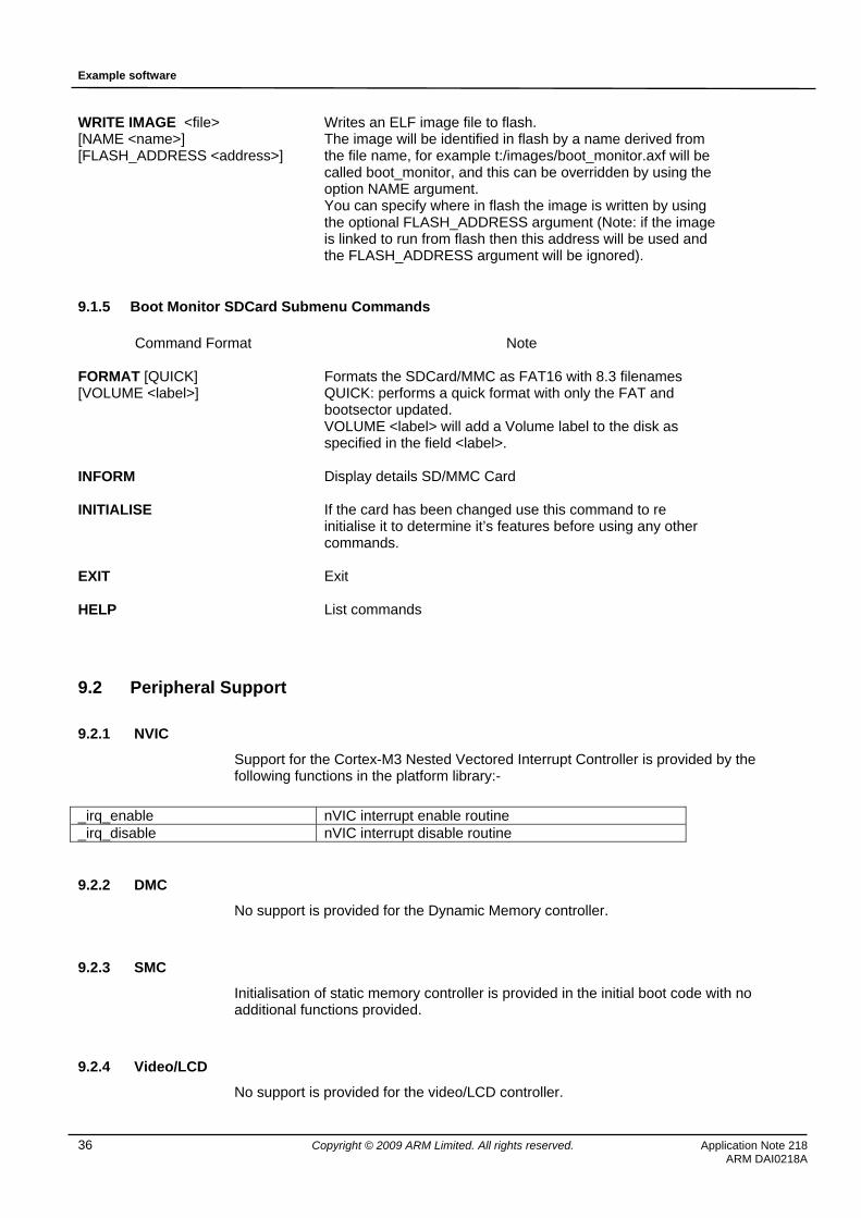
WRITE IMAGE <file> [NAME <name>] [FLASH_ADDRESS <address>]
Writes an ELF image file to flash. The image will be identified in flash by a name derived from the file name, for example t:/images/boot_monitor.axf will be called boot_monitor, and this can be overridden by using the option NAME argument. You can specify where in flash the image is written by using the optional FLASH_ADDRESS argument (Note: if the image is linked to run from flash then this address will be used and the FLASH_ADDRESS argument will be ignored).
9.1.5 Boot Monitor SDCard Submenu Commands
Command Format
Note
FORMAT [QUICK] [VOLUME <label>]
Formats the SDCard/MMC as FAT16 with 8.3 filenames QUICK: performs a quick format with only the FAT and bootsector updated. VOLUME <label> will add a Volume label to the disk as specified in the field <label>.
INFORM Display details SD/MMC Card
INITIALISE If the card has been changed use this command to re initialise it to determine it’s features before using any other commands.
EXIT Exit
HELP List commands
9.2 Peripheral Support
9.2.1 NVIC
Support for the Cortex-M3 Nested Vectored Interrupt Controller is provided by the following functions in the platform library:-
_irq_enable nVIC interrupt enable routine _irq_disable nVIC interrupt disable routine
9.2.2 DMC
No support is provided for the Dynamic Memory controller.
9.2.3 SMC
Initialisation of static memory controller is provided in the initial boot code with no additional functions provided.
9.2.4 Video/LCD
No support is provided for the video/LCD controller.
Example software
Application Note 218 Copyright © 2009 ARM Limited. All rights reserved. 37 ARM DAI0218A
9.2.5 UART
Support for the PL011 UART is provided by the following functions in the platform library:- _platform_uart_entry Handles all channel operations for the UART channels,
reading characters, writing characters and opening the channel.
9.2.6 Character LCD
Support for the character display is provided by the following functions in the platform library:-
_platform_charlcd_entry Handles all channel operations for the debug lcd
channel, writing characters and opening the channel.
9.2.7 Timer
Support for the SP804 timer is provided by the following functions in the platform library:- timer_enable Enables a timer with a given period and mode timer_disable Disables the defined timer timer_interrupt_clear Clears the timer interrupt
9.2.8 RTC
Support for the real time clock is provided by the command line interface commands SET DATE , SET TIME and by the following functions in the platform library:-
time Reads the current time from the Real Time Clock.
9.2.9 Ethernet
No support is provided for the Ethernet controller.
9.2.10 SSP
No support is provided for the SSP controller.
9.2.11 MMCI
Support for FAT16 file system 8.3 filenames 2GB max card size.
9.2.12 USB
No support is provided for the USB controller.
9.2.13 AACI
No support is provided for the AACI controller.
Example software
38 Copyright © 2009 ARM Limited. All rights reserved. Application Note 218 ARM DAI0218A
9.3 Hardware Requirements The firmware depends on various hardware facilities to be available to be able to provide its functionality.
9.3.1 Platform Library
The following items are basic requirements of the platform library without which a complete implementation would be difficult.
• UART – The default output for the C libraries standard I/O will normally be the first UART in the system. This UART is also use to output error messages when it is not possible to output them to the selected standard output device.
• 100Hz Counter – This is used to provide the clock function in the C library, having this counter removes the need to use a general purpose timer and allows a basic library to function without the need for interrupts.
• PrimeCell Real Time Clock (RTC) – This is used to provide the time function in the C library.
• The RTC during system initialization will be set to zero.
• 25MHz Counter – This is used to implement a general purpose delay routine which is used by a number of components within the firmware.
The following items enhance the functionality of the platform library but are not requirements, in fact in the case of the LCD and keyboard the platform library can be built without this support.
• LEDs – The firmware cycles the CPU LED’s when running standalone to show that the board is running correctly.
• The following items are only used by the platform library as a means to an end, therefore support is only required if needed.
• I2C – not used or implemented.
• Although not used by the platform library drivers are provided for the following.
• Character LCD – Support is provided for outputting messages to the character LCD using standard C library functions.
• Additional UARTs – Any additional UART can be accessed using C library standard functions.
9.3.2 Boot Monitor
The boot monitor requires the following hardware support.
• FAT file system – The boot monitor has several file related commands to copy, load, run etc. It also supports the use of script files which are stored in a FAT file system.
• Switches – The boot monitor uses one switch to select whether it will run a script when the system boots or not. This is user switch 1.
• Configuration and Informational – The boot monitor obtain information such as hardware revisions directly from the hardware register. The boot monitor can also configure system clocks by via hardware registers.
9.4 Endianness
The platform will only supports Little Endian (LE).
Example software
Application Note 218 Copyright © 2009 ARM Limited. All rights reserved. 39 ARM DAI0218A
9.5 Multiprocessing
The platform library will not support multiprocessing and therefore any image that is built with the platform library will only run on a single core.
9.6 System Boot
There are bootable devices on the board: NOR Flash or SSRAM.
9.6.1 Boot from Flash
When the system boots the first instructions executed will be from memory at address 0. This memory is read only. If the code within this memory requires read/write memory it is expected that it will initialize and use SSRAM. The type of memory visible at address 0 on system boot is determined by the configuration register settings, the default setting is to boot from flash. At system boot this memory will be visible in two locations, at address zero and at a fixed location in the memory map. It is expected that the code within this memory will branch to the copy at the fixed location. The code will detect if the core is a secondary master and if so enter a safe mode. Only the primary master will continue initialization and copy the code to SSRAM before performing a remap operation to remove the copy at address zero.
9.7 Platform Library Initialization The implementation is very similar to the existing ARM hardware platforms, therefore the initialization of the platform library will be basically the same. The differences are handled with different include files and conditional compilation.
9.8 Memory Management & Caches No cache or memory management is implemented in the processor so no additional support is required.
9.9 Building the Firmware
9.9.1 Development Environment
Currently, only a Windows development environment is supported. The firmware can be built using CodeWarrior and RVCT v3.1.
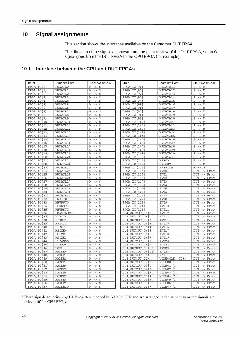
Signal assignments
40 Copyright © 2009 ARM Limited. All rights reserved. Application Note 218 ARM DAI0218A
10 Signal assignments This section shows the interfaces available on the Customer DUT FPGA.
The direction of the signals is shown from the point of view of the DUT FPGA, so an O signal goes from the DUT FPGA to the CPU FPGA (for example).
10.1 Interface between the CPU and DUT FPGAs
Bus Function Direction Bus Function Direction FPGA_IC[0] HWDATA0 M -> S FPGA_IC[90] HRDATA11 S -> M FPGA_IC[1] HWDATA1 M -> S FPGA_IC[91] HRDATA12 S -> M FPGA_IC[2] HWDATA2 M -> S FPGA_IC[92] HRDATA13 S -> M FPGA_IC[3] HWDATA3 M -> S FPGA_IC[93] HRDATA14 S -> M FPGA_IC[4] HWDATA4 M -> S FPGA_IC[94] HRDATA15 S -> M FPGA_IC[5] HWDATA5 M -> S FPGA_IC[95] HRDATA16 S -> M FPGA_IC[6] HWDATA6 M -> S FPGA_IC[96] HRDATA17 S -> M FPGA_IC[7] HWDATA7 M -> S FPGA_IC[97] HRDATA18 S -> M FPGA_IC[8] HWDATA8 M -> S FPGA_IC[98] HRDATA19 S -> M FPGA_IC[9] HWDATA9 M -> S FPGA_IC[99] HRDATA20 S -> M FPGA_IC[10] HWDATA10 M -> S FPGA_IC[100] HRDATA21 S -> M FPGA_IC[11] HWDATA11 M -> S FPGA_IC[101] HRDATA22 S -> M FPGA_IC[12] HWDATA12 M -> S FPGA_IC[102] HRDATA23 S -> M FPGA_IC[13] HWDATA13 M -> S FPGA_IC[103] HRDATA24 S -> M FPGA_IC[14] HWDATA14 M -> S FPGA_IC[104] HRDATA25 S -> M FPGA_IC[15] HWDATA15 M -> S FPGA_IC[105] HRDATA26 S -> M FPGA_IC[16] HWDATA16 M -> S FPGA_IC[106] HRDATA27 S -> M FPGA_IC[17] HWDATA17 M -> S FPGA_IC[107] HRDATA28 S -> M FPGA_IC[18] HWDATA18 M -> S FPGA_IC[108] HRDATA29 S -> M FPGA_IC[19] HWDATA19 M -> S FPGA_IC[109] HRDATA30 S -> M FPGA_IC[20] HWDATA20 M -> S FPGA_IC[110] HRDATA31 S -> M FPGA_IC[21] HWDATA21 M -> S FPGA_IC[111] HRESP S -> M FPGA_IC[22] HWDATA22 M -> S FPGA_IC[112] HREADY S -> M FPGA_IC[23] HWDATA23 M -> S FPGA_IC[113] HRESETn M -> S FPGA_IC[24] HWDATA24 M -> S FPGA_IC[114] INT0 DUT -> Proc FPGA_IC[25] HWDATA25 M -> S FPGA_IC[115] INT1 DUT -> Proc FPGA_IC[26] HWDATA26 M -> S FPGA_IC[116] INT2 DUT -> Proc FPGA_IC[27] HWDATA27 M -> S FPGA_IC[117] INT3 DUT -> Proc FPGA_IC[28] HWDATA28 M -> S FPGA_IC[118] INT4 DUT -> Proc FPGA_IC[29] HWDATA29 M -> S FPGA_IC[119] INT5 DUT -> Proc FPGA_IC[30] HWDATA30 M -> S FPGA_IC[120] INT6 DUT -> Proc FPGA_IC[31] HWDATA31 M -> S FPGA_IC[121] INT7 DUT -> Proc FPGA_IC[32] HWRITE M -> S FPGA_IC[122] INT8 DUT -> Proc FPGA_IC[33] HBURST0 M -> S FPGA_IC[123] INT9 DUT -> Proc FPGA_IC[34] HBURST1 M -> S FPGA_IC[124] INT10 DUT -> Proc FPGA_IC[35] HBURST2 M -> S FPGA_IC[125] INT11 DUT -> Proc FPGA_IC[36] HMASTLOCK M -> S L14_DUTOUT_DN[0] INT12 DUT -> Proc FPGA_IC[37] HPROT0 M -> S L14_DUTOUT_DN[1] INT13 DUT -> Proc FPGA_IC[38] HPROT1 M -> S L14_DUTOUT_DN[2] INT14 DUT -> Proc FPGA_IC[39] HPROT2 M -> S L14_DUTOUT_DN[3] INT15 DUT -> Proc FPGA_IC[40] HPROT3 M -> S L14_DUTOUT_DN[4] INT16 DUT -> Proc FPGA_IC[41] HSIZE0 M -> S L14_DUTOUT_DN[5] INT17 DUT -> Proc FPGA_IC[42] HSIZE1 M -> S L14_DUTOUT_DN[6] INT18 DUT -> Proc FPGA_IC[43] HSIZE2 M -> S L14_DUTOUT_DN[7] INT19 DUT -> Proc FPGA_IC[44] HTRANS0 M -> S L14_DUTOUT_DN[8] INT20 DUT -> Proc FPGA_IC[45] HTRANS1 M -> S L14_DUTOUT_DN[9] INT21 DUT -> Proc FPGA_IC[46] HSEL M -> S L14_DUTOUT_DN[10] INT22 DUT -> Proc FPGA_IC[47] HADDR0 M -> S L14_DUTOUT_DN[11] INT23 DUT -> Proc FPGA_IC[48] HADDR1 M -> S L14_DUTOUT_DN[12] NMI DUT -> Proc FPGA_IC[49] HADDR2 M -> S L14_DUTOUT_CLK VIDEOCLK (CLK) DUT -> Proc FPGA_IC[50] HADDR3 M -> S L14_DUTOUT_DP[0] VIDEO0 (1) DUT -> Proc FPGA_IC[51] HADDR4 M -> S L14_DUTOUT_DP[1] VIDEO1 (1) DUT -> Proc FPGA_IC[52] HADDR5 M -> S L14_DUTOUT_DP[2] VIDEO2 (1) DUT -> Proc FPGA_IC[53] HADDR6 M -> S L14_DUTOUT_DP[3] VIDEO3 (1) DUT -> Proc FPGA_IC[54] HADDR7 M -> S L14_DUTOUT_DP[4] VIDEO4 (1) DUT -> Proc FPGA_IC[55] HADDR8 M -> S L14_DUTOUT_DP[5] VIDEO5 (1) DUT -> Proc FPGA_IC[56] HADDR9 M -> S L14_DUTOUT_DP[6] VIDEO6 (1) DUT -> Proc FPGA_IC[57] HADDR10 M -> S L14_DUTOUT_DP[7] VIDEO7 (1) DUT -> Proc
1 These signals are driven by DDR registers clocked by VIDEOCLK and are arranged in the same way as the signals are
driven off the CPU FPGA.
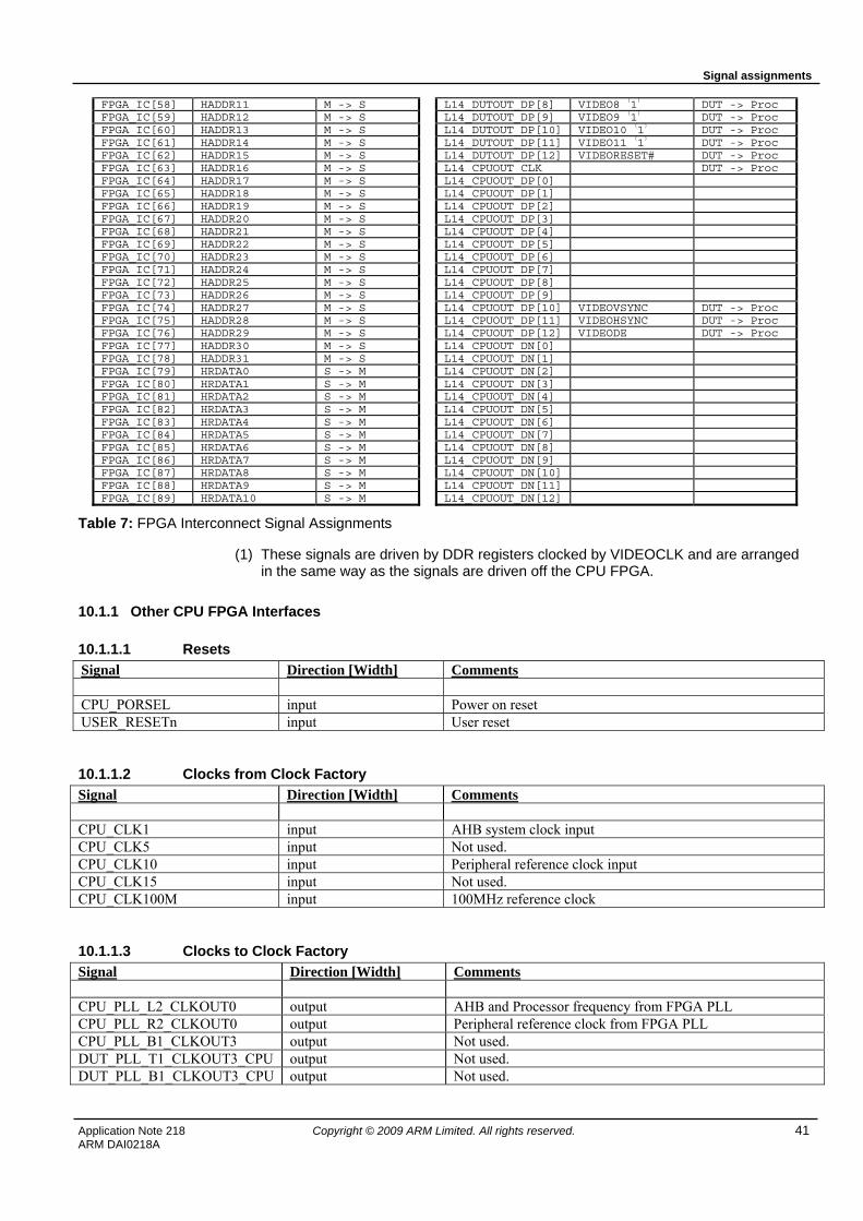
Signal assignments
Application Note 218 Copyright © 2009 ARM Limited. All rights reserved. 41 ARM DAI0218A
FPGA_IC[58] HADDR11 M -> S L14_DUTOUT_DP[8] VIDEO8 (1) DUT -> Proc FPGA_IC[59] HADDR12 M -> S L14_DUTOUT_DP[9] VIDEO9 (1) DUT -> Proc FPGA_IC[60] HADDR13 M -> S L14_DUTOUT_DP[10] VIDEO10 (1) DUT -> Proc FPGA_IC[61] HADDR14 M -> S L14_DUTOUT_DP[11] VIDEO11 (1) DUT -> Proc FPGA_IC[62] HADDR15 M -> S L14_DUTOUT_DP[12] VIDEORESET# DUT -> Proc FPGA_IC[63] HADDR16 M -> S L14_CPUOUT_CLK DUT -> Proc FPGA_IC[64] HADDR17 M -> S L14_CPUOUT_DP[0] FPGA_IC[65] HADDR18 M -> S L14_CPUOUT_DP[1] FPGA_IC[66] HADDR19 M -> S L14_CPUOUT_DP[2] FPGA_IC[67] HADDR20 M -> S L14_CPUOUT_DP[3] FPGA_IC[68] HADDR21 M -> S L14_CPUOUT_DP[4] FPGA_IC[69] HADDR22 M -> S L14_CPUOUT_DP[5] FPGA_IC[70] HADDR23 M -> S L14_CPUOUT_DP[6] FPGA_IC[71] HADDR24 M -> S L14_CPUOUT_DP[7] FPGA_IC[72] HADDR25 M -> S L14_CPUOUT_DP[8] FPGA_IC[73] HADDR26 M -> S L14_CPUOUT_DP[9] FPGA_IC[74] HADDR27 M -> S L14_CPUOUT_DP[10] VIDEOVSYNC DUT -> Proc FPGA_IC[75] HADDR28 M -> S L14_CPUOUT_DP[11] VIDEOHSYNC DUT -> Proc FPGA_IC[76] HADDR29 M -> S L14_CPUOUT_DP[12] VIDEODE DUT -> Proc FPGA_IC[77] HADDR30 M -> S L14_CPUOUT_DN[0] FPGA_IC[78] HADDR31 M -> S L14_CPUOUT_DN[1] FPGA_IC[79] HRDATA0 S -> M L14_CPUOUT_DN[2] FPGA_IC[80] HRDATA1 S -> M L14_CPUOUT_DN[3] FPGA_IC[81] HRDATA2 S -> M L14_CPUOUT_DN[4] FPGA_IC[82] HRDATA3 S -> M L14_CPUOUT_DN[5] FPGA_IC[83] HRDATA4 S -> M L14_CPUOUT_DN[6] FPGA_IC[84] HRDATA5 S -> M L14_CPUOUT_DN[7] FPGA_IC[85] HRDATA6 S -> M L14_CPUOUT_DN[8] FPGA_IC[86] HRDATA7 S -> M L14_CPUOUT_DN[9] FPGA_IC[87] HRDATA8 S -> M L14_CPUOUT_DN[10] FPGA_IC[88] HRDATA9 S -> M L14_CPUOUT_DN[11] FPGA_IC[89] HRDATA10 S -> M L14_CPUOUT_DN[12]
Table 7: FPGA Interconnect Signal Assignments
(1) These signals are driven by DDR registers clocked by VIDEOCLK and are arranged in the same way as the signals are driven off the CPU FPGA.
10.1.1 Other CPU FPGA Interfaces
10.1.1.1 Resets Signal Direction [Width] Comments CPU_PORSEL input Power on reset USER_RESETn input User reset
10.1.1.2 Clocks from Clock Factory Signal Direction [Width] Comments CPU_CLK1 input AHB system clock input CPU_CLK5 input Not used. CPU_CLK10 input Peripheral reference clock input CPU_CLK15 input Not used. CPU_CLK100M input 100MHz reference clock
10.1.1.3 Clocks to Clock Factory Signal Direction [Width] Comments CPU_PLL_L2_CLKOUT0 output AHB and Processor frequency from FPGA PLL CPU_PLL_R2_CLKOUT0 output Peripheral reference clock from FPGA PLL CPU_PLL_B1_CLKOUT3 output Not used. DUT_PLL_T1_CLKOUT3_CPU output Not used. DUT_PLL_B1_CLKOUT3_CPU output Not used.
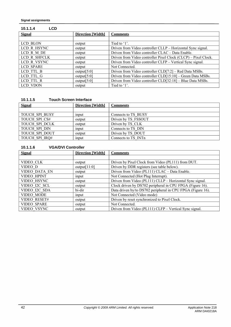
Signal assignments
42 Copyright © 2009 ARM Limited. All rights reserved. Application Note 218 ARM DAI0218A
10.1.1.4 LCD Signal Direction [Width] Comments LCD_BLON output Tied to ‘1’. LCD_R_HSYNC output Driven from Video controller CLLP – Horizontal Sync signal. LCD_R_M_DE output Driven from Video controller CLAC – Data Enable. LCD_R_SHFCLK output Driven from Video controller Pixel Clock (CLCP) – Pixel Clock. LCD_R_VSYNC output Driven from Video controller CLFP – Vertical Sync signal. LCD_SPARE output Not Connected. LCD_TTL_B output[5:0] Driven from Video controller CLD[7:2] – Red Data MSBs. LCD_TTL_G output[5:0] Driven from Video controller CLD[15:10] – Green Data MSBs. LCD_TTL_R output[5:0] Driven from Video controller CLD[32:18] – Blue Data MSBs. LCD_VDON output Tied to ‘1’.
10.1.1.5 Touch Screen Interface Signal Direction [Width] Comments TOUCH_SPI_BUSY input Connects to TS_BUSY TOUCH_SPI_CS# output Driven by TS_FSSOUT TOUCH_SPI_DCLK output Driven by TS_CLK TOUCH_SPI_DIN input Connects to TS_DIN TOUCH_SPI_DOUT output Driven by TS_DOUT TOUCH_SPI_IRQ# input Connects to TS_INTn
10.1.1.6 VGA/DVI Controller Signal Direction [Width] Comments VIDEO_CLK output Driven by Pixel Clock from Video (PL111) from DUT. VIDEO_D output[11:0] Driven by DDR registers (see table below). VIDEO_DATA_EN output Driven from Video (PL111) CLAC – Data Enable. VIDEO_HPINT input Not Connected (Hot Plug Interrupt). VIDEO_HSYNC output Driven from Video (PL111) CLLP – Horizontal Sync signal. VIDEO_I2C_SCL output Clock driven by DS702 peripheral in CPU FPGA (Figure 16). VIDEO_I2C_SDA bi-dir Data driven by/to DS702 peripheral in CPU FPGA (Figure 16). VIDEO_MODE input Not Connected (Video mode) VIDEO_RESET# output Driven by reset synchronized to Pixel Clock. VIDEO_SPARE output Not Connected. VIDEO_VSYNC output Driven from Video (PL111) CLFP – Vertical Sync signal.
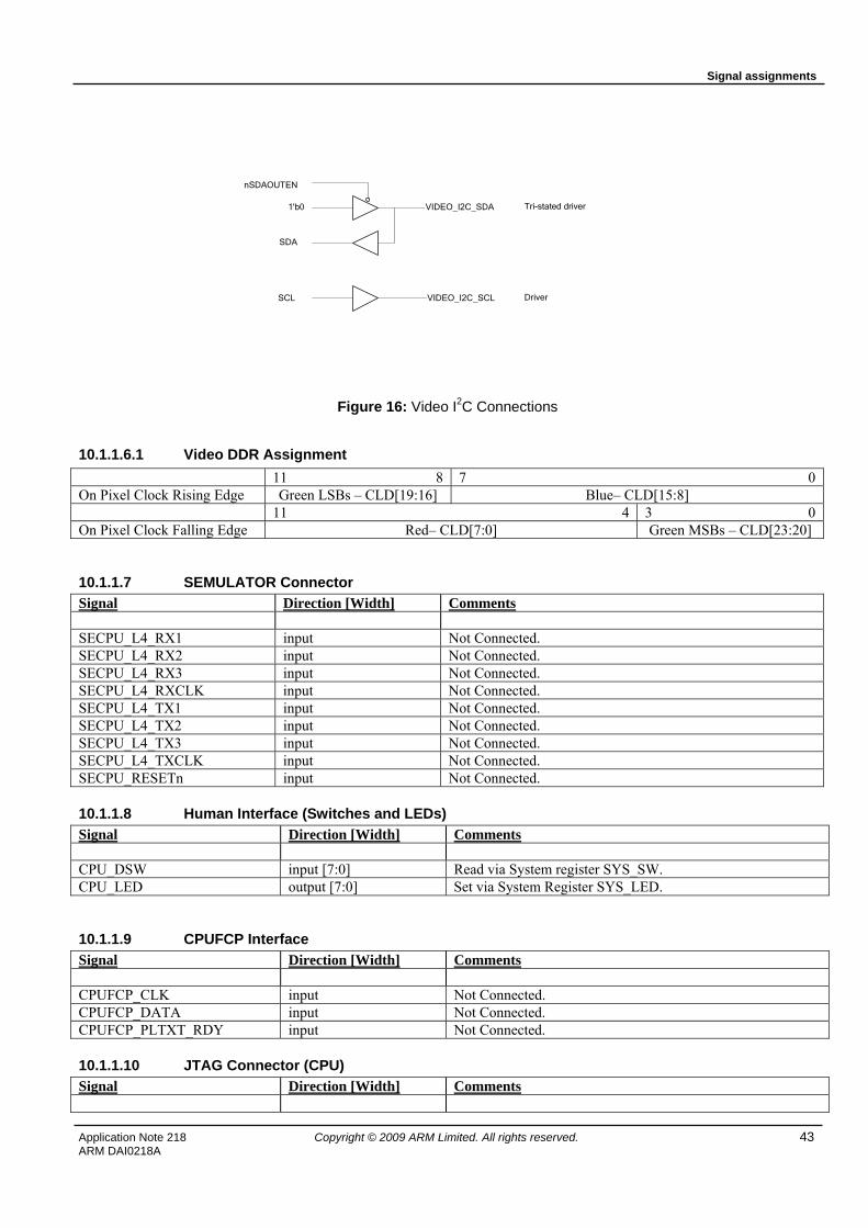
Signal assignments
Application Note 218 Copyright © 2009 ARM Limited. All rights reserved. 43 ARM DAI0218A
nSDAOUTEN
1'b0 VIDEO_I2C_SDA
SCL VIDEO_I2C_SCL
Tri-stated driver
Driver
SDA
Figure 16: Video I2C Connections
10.1.1.6.1 Video DDR Assignment 11 8 7 0 On Pixel Clock Rising Edge Green LSBs – CLD[19:16] Blue– CLD[15:8] 11 4 3 0 On Pixel Clock Falling Edge Red– CLD[7:0] Green MSBs – CLD[23:20]
10.1.1.7 SEMULATOR Connector Signal Direction [Width] Comments SECPU_L4_RX1 input Not Connected. SECPU_L4_RX2 input Not Connected. SECPU_L4_RX3 input Not Connected. SECPU_L4_RXCLK input Not Connected. SECPU_L4_TX1 input Not Connected. SECPU_L4_TX2 input Not Connected. SECPU_L4_TX3 input Not Connected. SECPU_L4_TXCLK input Not Connected. SECPU_RESETn input Not Connected.
10.1.1.8 Human Interface (Switches and LEDs) Signal Direction [Width] Comments CPU_DSW input [7:0] Read via System register SYS_SW. CPU_LED output [7:0] Set via System Register SYS_LED.
10.1.1.9 CPUFCP Interface Signal Direction [Width] Comments CPUFCP_CLK input Not Connected. CPUFCP_DATA input Not Connected. CPUFCP_PLTXT_RDY input Not Connected.
10.1.1.10 JTAG Connector (CPU) Signal Direction [Width] Comments
Signal assignments
44 Copyright © 2009 ARM Limited. All rights reserved. Application Note 218 ARM DAI0218A
FTSH_GNDDET bi-dir Connector Detect. Weak pull-up on FPGA which is pulled low by the connector to indicate a connection.
FTSH_TMS bi-dir Input to SWDIOTMS on processor. Also used as Data Out for Serial Wire Debug.
FTSH_TCK bi-dir JTAG Clock to processor. FTSH_TDO bi-dir JTAG Data Out from processor. FTSH_TDI bi-dir JTAG Data In to processor. FTSH_TRST bi-dir JTAG Reset. This is an active low signal.
10.1.1.11 JTAG Connector (Shared) Signal Direction [Width] Comments INTCPU_TDI input JTAG Data In to processor. INTCPU_TDO bi-dir JTAG Data Out from processor. INTCPU_TCK input JTAG Clock to processor. INTCPU_TMS input Input to TMS on processor. This is not connected to the Serial
Wire Debug Data Out. INTCPU_TRSTn input JTAG Reset. This is an active low signal. INTCPU_SRSTn input Factored into CPU reset. INTCPU_RTCK output Not connected. INTCPU_DBGRQ input Not connected. INTCPU_DBGACK output Not connected.
10.1.1.12 MICTOR.Connections Signal Direction [Width] Comments MICTOR_PIPESTAT0 output Tied to ‘0’. MICTOR_PIPESTAT1 output Tied to ‘0’. MICTOR_PIPESTAT2 output Tied to ‘0’. MICTOR_EXTTRIG output Tied to ‘0’. MICTOR_TRACEPKT output[15:0] Bits [3:0] carry the TRACEDATA port from the processor.
Bits [15:4] are tied to ‘0’. MICTOR_TRACESYNC output Not connected. MICTOR_TRACECLK output Connects to processor TRACECLK port.
10.1.1.13 SSRAM Shared Connections Signal Direction [Width] Comments SSRAM_CLK output Driven by processor bus clock.
10.1.1.14 SSRAM 0 Connections
This port is driven by a dedicated interface control block which is not configurable and is transparent to the system.
Signal Direction [Width] Comments SSRAM0_A output [19:0] Address to SSRAM. SSRAM0_DQA bi-dir [7:0] Data lines [7:0]. Byte lane 0. SSRAM0_DQB bi-dir [7:0] Data lines [15:8]. Byte lane 1. SSRAM0_DQC bi-dir [7:0] Data lines [23:16]. Byte lane 2. SSRAM0_DQD bi-dir [7:0] Data lines [31:24]. Byte lane 3. SSRAM0_BWAn output Write byte lane 0. Active low signal. SSRAM0_BWBn output Write byte lane 1. Active low signal. SSRAM0_BWCn output Write byte lane 2. Active low signal.
Signal assignments
Application Note 218 Copyright © 2009 ARM Limited. All rights reserved. 45 ARM DAI0218A
SSRAM0_BWDn output Write byte lane 3. Active low signal. SSRAM0_DQPA bi-dir Byte lane 0 parity signal. SSRAM0_DQPB bi-dir Byte lane 1 parity signal. SSRAM0_DQPC bi-dir Byte lane 2 parity signal. SSRAM0_DQPD bi-dir Byte lane 3 parity signal. SSRAM0_CS1n output Chip select 1. Active low signal. SSRAM0_CS2 output Chip select 2. Active high signal. SSRAM0_CS3n output Chip select 3. Active low signal. SSRAM0_WEn output Write enable. Active low signal. SSRAM0_CKEn output Clock enable signal. Active low signal. SSRAM0_OEn output Output enable. Active low signal. SSRAM0_LBOn output Burst Mode Control. Active low signal. Tied to ‘0’. SSRAM0_ADV output Address Advance. Tied to ‘0’. SSRAM0_ZZ output Sleep request. Tied to ‘0’.
10.1.1.15 Common SSRAM1 and FLASH Connections
The lines shared between these devices are controlled by a multiplexer which is controlled by the interface controller for the FLASH RAM.
Signal Direction [Width] Comments SSRAMFLASH_A output [23:0] Address to SSRAM/FLASH. SSRAMFLASH_DQA bi-dir [7:0] Data lines [7:0]. Byte lane 0. SSRAMFLASH_DQB bi-dir [7:0] Data lines [15:8]. Byte lane 1. SSRAMFLASH_DQC bi-dir [7:0] Data lines [23:16]. Byte lane 2. SSRAMFLASH_DQD bi-dir [7:0] Data lines [31:24]. Byte lane 3.
10.1.1.16 SSRAM1 Connections
This port is driven by a dedicated interface control block which is not configurable and is transparent to the system.
Signal Direction [Width] Comments SSRAM1_BWAn output Write byte lane 0. Active low signal. SSRAM1_BWBn output Write byte lane 1. Active low signal. SSRAM1_BWCn output Write byte lane 2. Active low signal. SSRAM1_BWDn output Write byte lane 3. Active low signal. SSRAM1_DQPA bi-dir Byte lane 0 parity signal. SSRAM1_DQPB bi-dir Byte lane 1 parity signal. SSRAM1_DQPC bi-dir Byte lane 2 parity signal. SSRAM1_DQPD bi-dir Byte lane 3 parity signal. SSRAM1_CS1n output Chip select 1. Active low signal. SSRAM1_CS2 output Chip select 2. Active high signal. SSRAM1_CS3n output Chip select 3. Active low signal. SSRAM1_WEn output Write enable. Active low signal. SSRAM1_CKEn output Clock enable signal. Active low signal. SSRAM1_OEn output Output enable. Active low signal. SSRAM1_LBOn output Burst Mode Control. Active low signal. Tied to ‘0’. SSRAM1_ADV output Address Advance. Tied to ‘0’. SSRAM1_ZZ output Sleep request. Tied to ‘0’.
10.1.1.17 FLASH connections
This port is driven by a dedicated interface control block which is not configurable and is transparent to the system. This block is responsible for controlling the multiplexing of the shared data and address lines for these devices.
Signal assignments
46 Copyright © 2009 ARM Limited. All rights reserved. Application Note 218 ARM DAI0218A
Signal Direction [Width] Comments FLASH_WEn output Write enable. Active low signal. FLASH_RESETn output Memory reset. Active low signal. FLASH_CEn output Chip select. Active low signal. FLASH_OEn output Output enable. Active low signal. FLASH_WPn_ACC output Not Write Protect/Access signal. Tied to ‘1’. No write
protection is available on this interface. FLASH_RD_BYn input Ready/ Not Busy input. Not connected.
10.1.1.18 RS232 connection
These interface is driven by the Primecell PL011. (see section 5.3.10). There is one UART in the example system connected to the CPU FPGA. Interface RS1 connects to UART 0.
Signal Direction [Width] Comments RS1_RXD_LVTTL input RS1_TXD_LVTTL output
10.1.2 Other DUT FPGA interfaces
10.1.2.1 Clocks and Resets
(see section 3.2) Signal Direction [Width] Comments USER_RESETn input HPE_RESETn input DUT_CLK1 input AHB system clock input DUT_CLK4 input Video Pixel Clock input DUT_CLK10 input Peripheral reference clock input DUT_CLK13 input AACI bit clock input DUT_CLK100M input Reference 100MHz input DUT_PLL_B1_CLKOUT3 output 25MHz reference clock from FPGA PLL DUT_PLL_R2_CLKOUT0 output AACI 24.576MHz bit clock x2 from FPGA PLL DUT_PLL_T1_CLKOUT3 output Video Pixel Clock from FPGA PLL
10.1.2.2 LED and switch connections
Please refer to section 5.3 for details on driving this interface. The buttons and switches can be read via the register SYS_SW (see section 5.3.1.3).
The values held in the SYS_LED and SYS_7SEG registers (see sections 5.3.1.4 and 5.3.1.5) are driven onto this interface based upon the value held in the HUMI_MODE field in the SYS_PERCFG register (see section 5.3.1.2).
The scheduler runs at a preset rate of 500Hz and selects a new driver for the data lines (DUT_HUMI_{A-G,DP}n) every 2 ms if the HUMI_MODE field is set to Scheduler (3’b000). The order of the cycle is:
- LEDs selected the scheduler drives DUT_HUMI_LEDn low.
- Segment 0 the scheduler drives DUT_HUMI_SEGn to 4’b1110.
- Segment 1 the scheduler drives DUT_HUMI_SEGn to 4’b1101.
- Segment 2 the scheduler drives DUT_HUMI_SEGn to 4’b1011.
- Segment 3 the scheduler drives DUT_HUMI_SEGn to 4’b0111.
Signal assignments
Application Note 218 Copyright © 2009 ARM Limited. All rights reserved. 47 ARM DAI0218A
- Character LCD the scheduler drives DUT_HUMI_SEGn to 4’b1110 and DUT_HUMI_LEDn high and enables the DUT_LCD_* interface control lines.
Should any operation be in progress when the scheduler wishes to switch back to the LED, then change is halted whilst the operation completes and any new operation is prevented from starting (the CharLCD driver appears busy to the processor).
Signal Direction [Width] Comments BUTTON input[4] DUT_DSW input[4] DUT_HUMI_An bi-dir DUT_HUMI_Bn bi-dir DUT_HUMI_Cn bi-dir DUT_HUMI_Dn bi-dir DUT_HUMI_En bi-dir DUT_HUMI_Fn bi-dir DUT_HUMI_Gn bi-dir DUT_HUMI_DPn bi-dir DUT_HUMI_SEGn output[4] DUT_HUMI_LEDn output DUT_LCD_REGSEL output DUT_LCD_RW output DUT_LCD_ENABLE output
10.1.2.3 FPGA Configuration connections These connector is not used by the design, but for FPGA configuration only. Signal Direction [Width] Comments DUTFCP_CLK input DUTFCP_DATA input DUTFCP_PLTXT_RDY input
10.1.2.4 SEMULATOR connections The SEmulator connector is not used by this design. For further details please refer to the MPB User Guide [1]. Signal Direction [Width] Comments SEDUT_L4_RXN input[4] SEDUT_L4_RXP input[4] SEDUT_L4_RXCLKN input SEDUT_L4_RXCLKP input SEDUT_L4_TXN input[4] SEDUT_L4_TXP input[4] SEDUT_L4_TXCLKN input SEDUT_L4_TXCLKP input SEDUT_RESETn input
Signal assignments
48 Copyright © 2009 ARM Limited. All rights reserved. Application Note 218 ARM DAI0218A
10.1.2.5 USB Interface
This interface is driven by a dedicated interface driver which is designed to drive the NXP ISP1761 USB controller [14]. The interface driver is not configurable and is transparent to the rest of the system.
Signal Direction [Width] Comments USB_A output[17] USB_CSn output USB_RDn output USB_WRn output USB_D bi-dir[16] USB_DC_DACK bi-dir Not connected in this design. USB_DC_DREQ bi-dir Not connected in this design. USB_DC_IRQ bi-dir Used as input only. See interrupt table. USB_DC_WAKEUPn bi-dir Not connected in this design. USB_HC_DACK bi-dir Not connected in this design. USB_HC_DREQ bi-dir Not connected in this design. USB_HC_IRQ bi-dir Used as input only. See interrupt table. USB_HC_WAKEUPn bi-dir Not connected in this design.
10.1.2.6 Multi-Media/SD Card Interface
This interface is driven by the Primecell PL181 (see section 5.3.12). Signal Direction [Width] Comments SD_SCLK output Driven by MCICLKOUT. SD_CD input See Figure 17 SD_WRP input See Figure 17 SD_CT output Pulled low to enable SD_CD and SD_WRP inputs SD_IRQ bi-dir See Figure 17 SD_CSn bi-dir See Figure 17 SD_DAT bi-dir See Figure 17 SD_DI bi-dir See Figure 17 SD_DO bi-dir See Figure 17
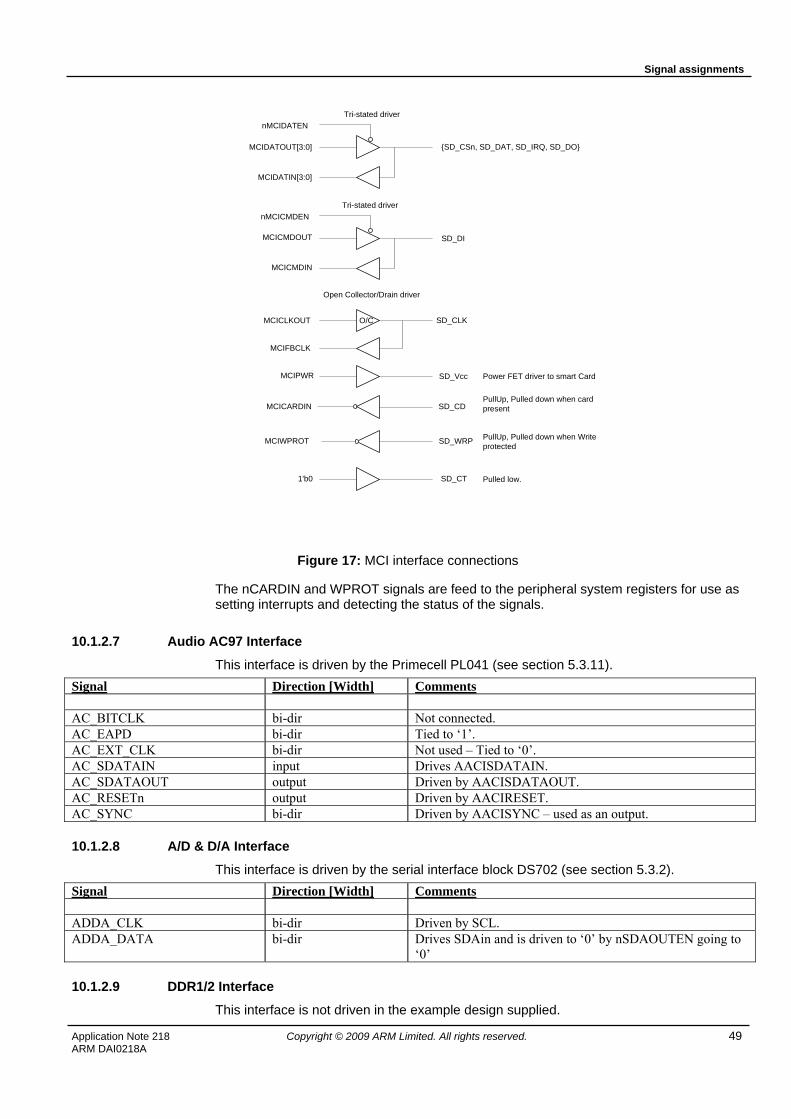
Signal assignments
Application Note 218 Copyright © 2009 ARM Limited. All rights reserved. 49 ARM DAI0218A
MCICMDOUT SD_DI
MCICMDIN
MCICLKOUT SD_CLK
MCIPWR SD_Vcc
SD_CDMCICARDIN
Power FET driver to smart Card
O/C
PullUp, Pulled down when Write protected
Tri-stated driver
Open Collector/Drain driver
MCIFBCLK
SD_WRPMCIWPROT
PullUp, Pulled down when card present
Pulled low.SD_CT1'b0
nMCICMDEN
{SD_CSn, SD_DAT, SD_IRQ, SD_DO}
Tri-stated driver
MCIDATOUT[3:0]
MCIDATIN[3:0]
nMCIDATEN
Figure 17: MCI interface connections
The nCARDIN and WPROT signals are feed to the peripheral system registers for use as setting interrupts and detecting the status of the signals.
10.1.2.7 Audio AC97 Interface
This interface is driven by the Primecell PL041 (see section 5.3.11). Signal Direction [Width] Comments AC_BITCLK bi-dir Not connected. AC_EAPD bi-dir Tied to ‘1’. AC_EXT_CLK bi-dir Not used – Tied to ‘0’. AC_SDATAIN input Drives AACISDATAIN. AC_SDATAOUT output Driven by AACISDATAOUT. AC_RESETn output Driven by AACIRESET. AC_SYNC bi-dir Driven by AACISYNC – used as an output.
10.1.2.8 A/D & D/A Interface
This interface is driven by the serial interface block DS702 (see section 5.3.2). Signal Direction [Width] Comments ADDA_CLK bi-dir Driven by SCL. ADDA_DATA bi-dir Drives SDAin and is driven to ‘0’ by nSDAOUTEN going to
‘0’
10.1.2.9 DDR1/2 Interface
This interface is not driven in the example design supplied.
Signal assignments
50 Copyright © 2009 ARM Limited. All rights reserved. Application Note 218 ARM DAI0218A
Signal Direction [Width] Comments MEM_DDR2_ADDR output[15:0] MEM_DDR2_BA output[2:0] MEM_DDR2_CASn output MEM_DDR2_RASn output MEM_DDR2_WEn output MEM_DDR2_CSn output[1:0] MEM_DDR2_ODT output[1:0] MEM_DDR2_CKE output[1:0] MEM_DDR2_CLKP output[1:0] MEM_DDR2_CLKN output[1:0] MEM_DDR2_DM output[3:0] MEM_DDR2_DQSN bi-dir[3:0] MEM_DDR2_DQSP bi-dir[3:0] MEM_DDR2_DQ bi-dir[31:0] MEM_VAR bi-dir[23:0] Not connected in this design.
10.1.2.10 Ethernet Phy Interface
This interface is not driven in the example design supplied. Signal Direction [Width] Comments ETH_COL bi-dir ETH_CRS bi-dir ETH_MDC bi-dir ETH_MDINTRn bi-dir ETH_RESETn bi-dir ETH_RXCLK bi-dir ETH_RXD bi-dir[3:0] ETH_RXDV bi-dir ETH_RXER bi-dir ETH_TXCLK bi-dir ETH_TXD bi-dir[3:0] ETH_TXEN bi-dir ETH_TXER bi-dir
10.1.2.11 CAN Interface
This interface is not driven in the example design supplied. Signal Direction [Width] Comments CAN_RXD bi-dir CAN_TXD bi-dir CAN_STB bi-dir
10.1.2.12 Flexray Interface
This interface is not driven in the example design supplied. Signal Direction [Width] Comments FLEX_BGE bi-dir FLEX_EN bi-dir FLEX_ERRn bi-dir FLEX_RXD bi-dir FLEX_RXEN bi-dir FLEX_STBn bi-dir FLEX_TXD bi-dir FLEX_TXEN bi-dir
Signal assignments
Application Note 218 Copyright © 2009 ARM Limited. All rights reserved. 51 ARM DAI0218A
FLEX_WAKE bi-dir
10.1.2.13 LIN Interface
This interface is not driven in the example design supplied. Signal Direction [Width] Comments LIN_RXD bi-dir LIN_TXD bi-dir LIN_SLPn bi-dir LIN_ACTIVE bi-dir
10.1.2.14 RS232 connections
These interfaces are driven by the Primecell PL011. (see section 5.3.10). There are three UARTs in the example system connected to the DUT FPGA. Interface RS0 connects to UART 1, UARTS 2 and 3 are connected to the UART ports RS232-1 and RS232-2 on the baseboard respectively (RS0_xxx_MIDI and RS1_xxx_MIDI).
Signal Direction [Width] Comments RS0_RXD_LVTTL input RS0_TXD_LVTTL output RS0_CTS_LVTTL input RS0_RTS_LVTTL output RS0_RXD_MIDI input RS0_TXD_MIDI output RS1_RXD_MIDI input RS1_TXD_MIDI output


![Onthemathematicaltreatmentofthe Born … · 1 Introduction. In the paper [SW1] (see also [SW2, SW3]), the authors made a remarkable effort to un- ... It was certainly not a easy](https://img.pdfslide.us/doc/110x75/5fae1b15e549041e9d7aa51f/onthemathematicaltreatmentofthe-born-1-introduction-in-the-paper-sw1-see-also.jpg)