Embed Size (px)
Citation preview
Microcontroller Applications
1
RevisionRevision

Binary ArithmeticBinary Arithmetic
2
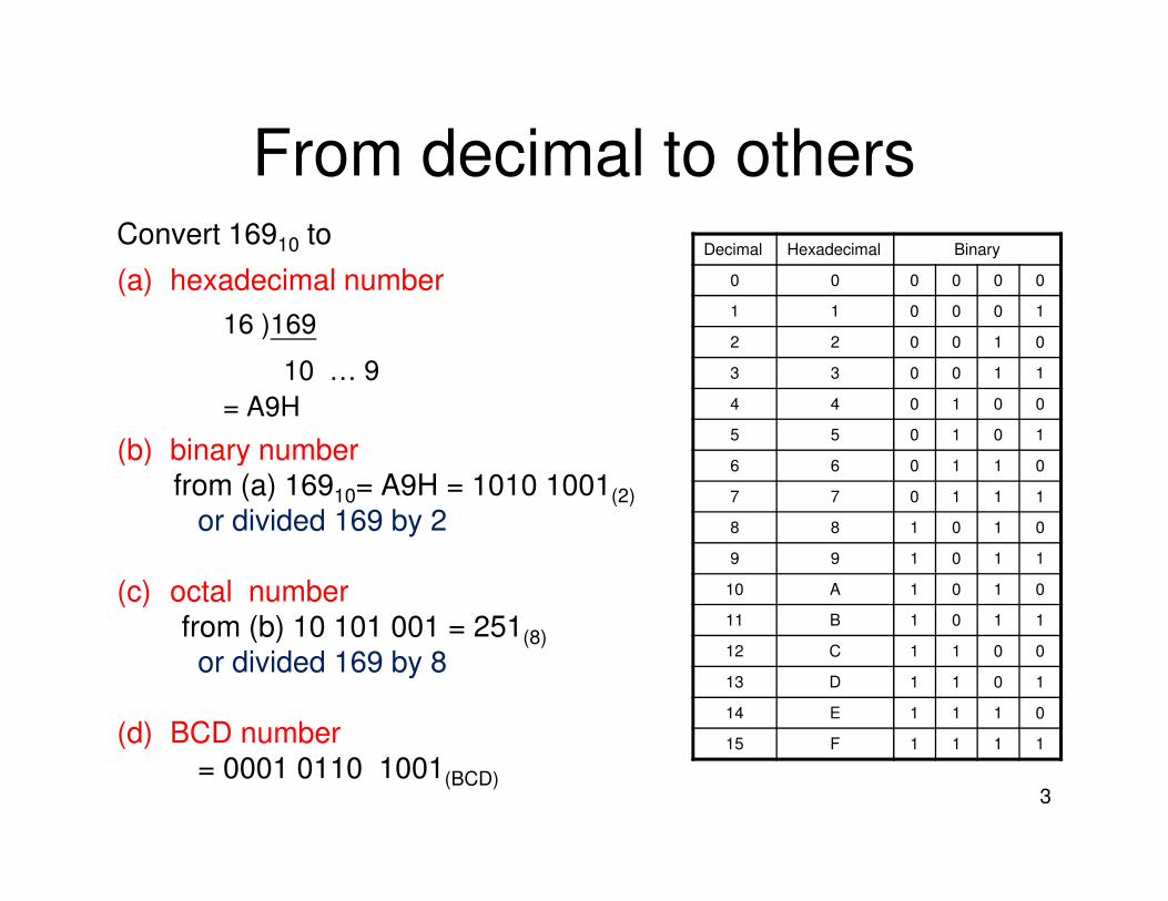
From decimal to othersConvert 16910 to
(a) hexadecimal number
16 )169
10 … 9
= A9H
(b) binary number
Decimal Hexadecimal Binary
0 0 0 0 0 0
1 1 0 0 0 1
2 2 0 0 1 0
3 3 0 0 1 1
4 4 0 1 0 0
5 5 0 1 0 1
3
(b) binary numberfrom (a) 16910= A9H = 1010 1001(2)
or divided 169 by 2
(c) octal numberfrom (b) 10 101 001 = 251(8)
or divided 169 by 8
(d) BCD number= 0001 0110 1001(BCD)
6 6 0 1 1 0
7 7 0 1 1 1
8 8 1 0 1 0
9 9 1 0 1 1
10 A 1 0 1 0
11 B 1 0 1 1
12 C 1 1 0 0
13 D 1 1 0 1
14 E 1 1 1 0
15 F 1 1 1 1
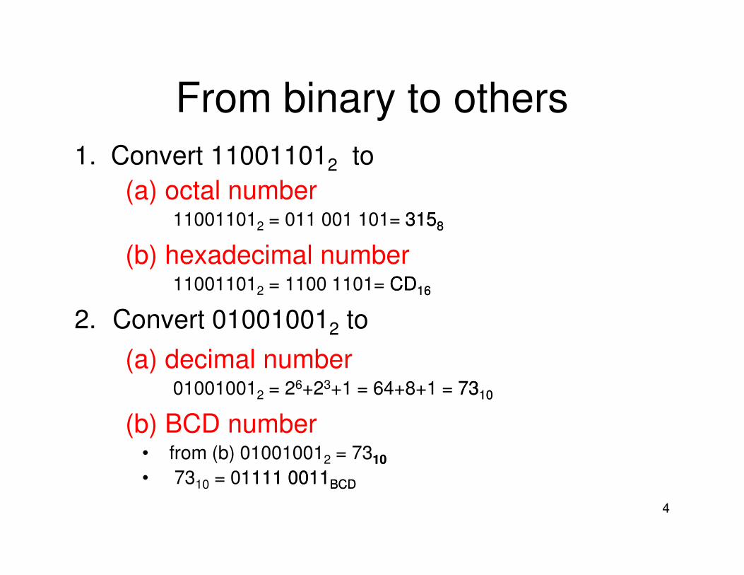
From binary to others
1. Convert 110011012 to
(a) octal number 110011012 = 011 001 101= 31531588
(b) hexadecimal number 110011012 = 1100 1101= CDCD1616
4
110011012 = 1100 1101= CDCD1616
2. Convert 010010012 to
(a) decimal number010010012 = 26+23+1 = 64+8+1 = 73731010
(b) BCD number• from (b) 010010012 = 731010
• 7310 = 01111 00111111 0011BCDBCD
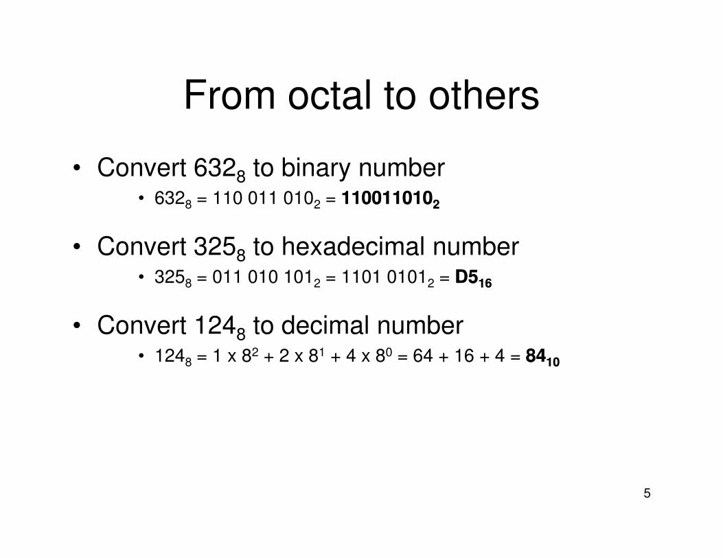
From octal to others
• Convert 6328 to binary number • 6328 = 110 011 0102 = 11001101011001101022
• Convert 3258 to hexadecimal number • 3258 = 011 010 1012 = 1101 01012 = D5D51616
5
• 3258 = 011 010 1012 = 1101 01012 = D5D51616
• Convert 1248 to decimal number• 1248 = 1 x 82 + 2 x 81 + 4 x 80 = 64 + 16 + 4 = 84841010
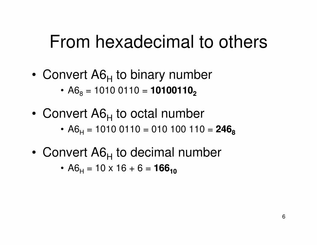
From hexadecimal to others
• Convert A6H to binary number • A68 = 1010 0110 = 101001101010011022
• Convert A6H to octal number
6
H
• A6H = 1010 0110 = 010 100 110 = 24624688
• Convert A6H to decimal number• A6H = 10 x 16 + 6 = 1661661010
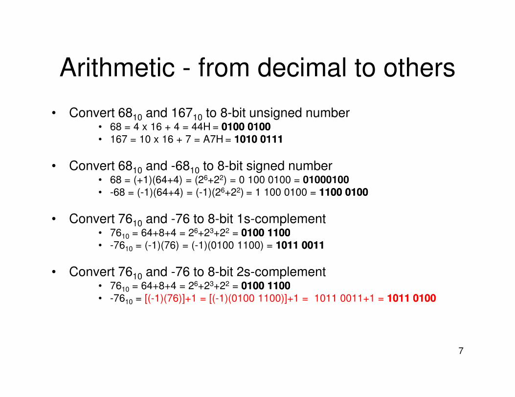
Arithmetic - from decimal to others
• Convert 6810 and 16710 to 8-bit unsigned number• 68 = 4 x 16 + 4 = 44H = 0100 01000100 0100
• 167 = 10 x 16 + 7 = A7H = 1010 01111010 0111
• Convert 6810 and -6810 to 8-bit signed number• 68 = (+1)(64+4) = (26+22) = 0 100 0100 = 01000100
• -68 = (-1)(64+4) = (-1)(26+22) = 1 100 0100 = 1100 01001100 0100
7
• Convert 7610 and -76 to 8-bit 1s-complement• 7610 = 64+8+4 = 26+23+22 = 0100 11000100 1100
• -7610 = (-1)(76) = (-1)(0100 1100) = 1011 00111011 0011
• Convert 7610 and -76 to 8-bit 2s-complement• 7610 = 64+8+4 = 26+23+22 = 0100 11000100 1100
• -7610 = [(-1)(76)]+1 = [(-1)(0100 1100)]+1 = 1011 0011+1 = 1011 01001011 0100
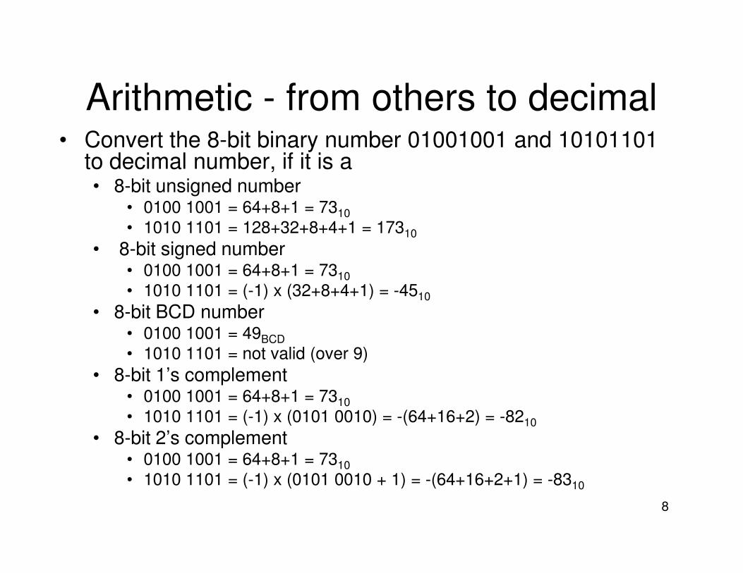
Arithmetic - from others to decimal• Convert the 8-bit binary number 01001001 and 10101101
to decimal number, if it is a • 8-bit unsigned number
• 0100 1001 = 64+8+1 = 7310
• 1010 1101 = 128+32+8+4+1 = 17310
• 8-bit signed number• 0100 1001 = 64+8+1 = 7310
• 1010 1101 = (-1) x (32+8+4+1) = -45
8
• 1010 1101 = (-1) x (32+8+4+1) = -4510
• 8-bit BCD number• 0100 1001 = 49BCD
• 1010 1101 = not valid (over 9)
• 8-bit 1’s complement• 0100 1001 = 64+8+1 = 7310
• 1010 1101 = (-1) x (0101 0010) = -(64+16+2) = -8210
• 8-bit 2’s complement• 0100 1001 = 64+8+1 = 7310
• 1010 1101 = (-1) x (0101 0010 + 1) = -(64+16+2+1) = -8310
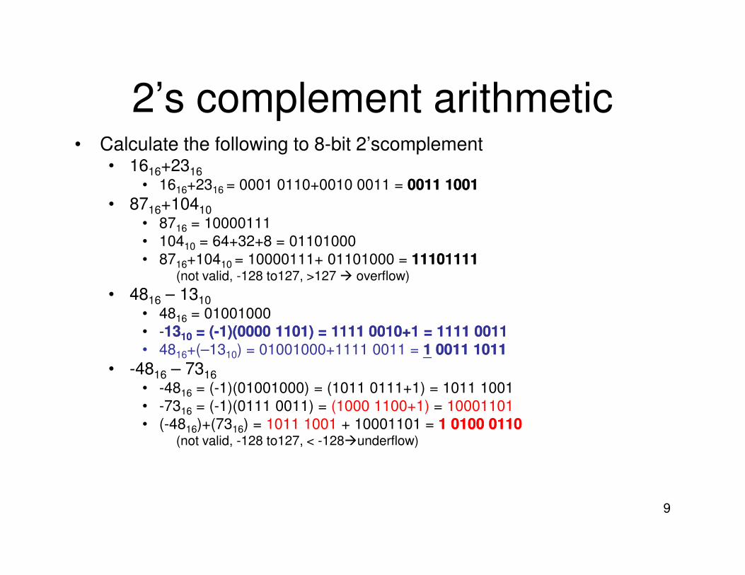
2’s complement arithmetic• Calculate the following to 8-bit 2’scomplement
• 1616+2316
• 1616+2316 = 0001 0110+0010 0011 = 0011 10010011 1001
• 8716+10410
• 8716 = 10000111
• 10410 = 64+32+8 = 01101000
• 8716+10410 = 10000111+ 01101000 = 1110111111101111(not valid, -128 to127, >127 � overflow)
• 48 – 13
9
• 4816 – 1310
• 4816 = 01001000
• -13131010 = (= (--1)(0000 1101) = 1111 0010+1 = 1111 00111)(0000 1101) = 1111 0010+1 = 1111 0011
• 4816+(–1310) = 01001000+1111 0011 = 11 0011 10110011 1011
• -4816 – 7316
• -4816 = (-1)(01001000) = (1011 0111+1) = 1011 1001
• -7316 = (-1)(0111 0011) = (1000 1100+1) = 10001101
• (-4816)+(7316) = 1011 1001 + 10001101 = 1 0100 01101 0100 0110(not valid, -128 to127, < -128�underflow)
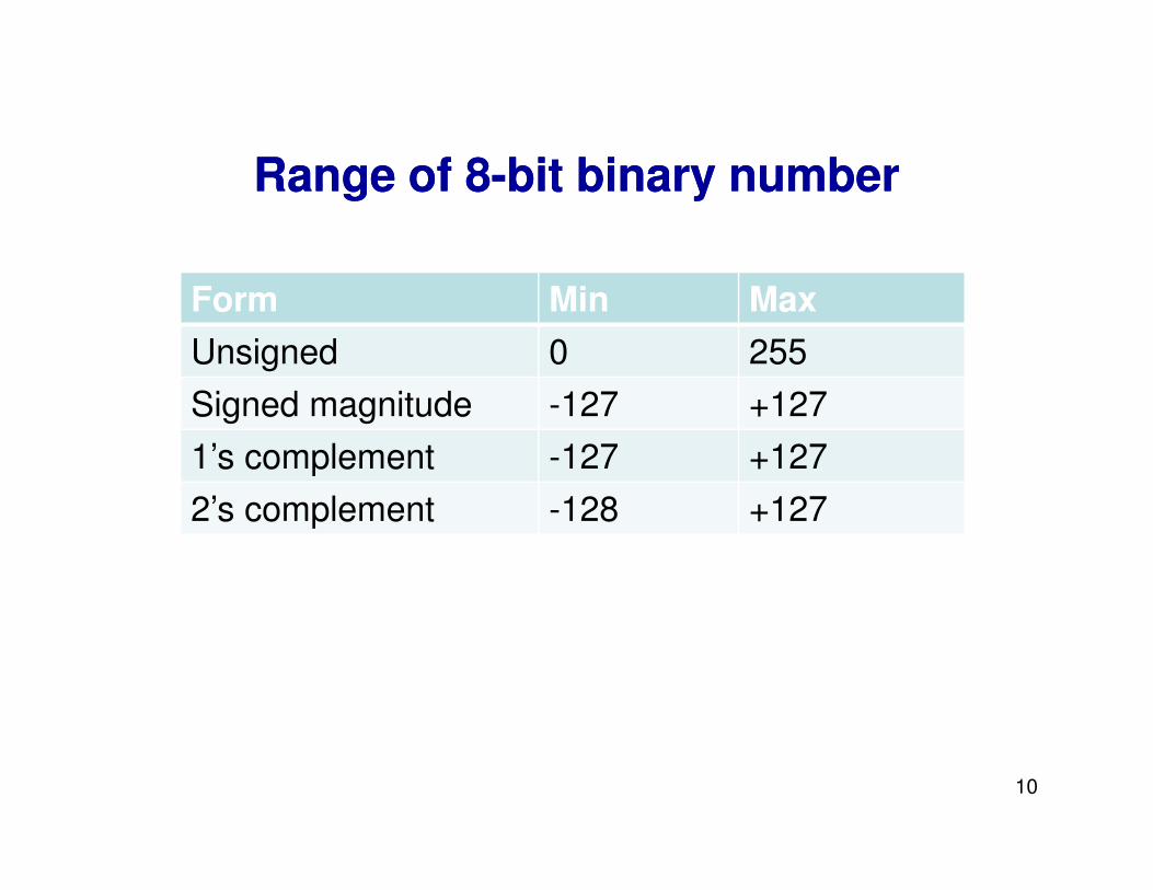
Range of 8Range of 8--bit binary numberbit binary number
Form Min Max
Unsigned 0 255
Signed magnitude -127 +127
1’s complement -127 +127
10
1’s complement -127 +127
2’s complement -128 +127

ArchitectureArchitecture
11
ArchitectureArchitecture
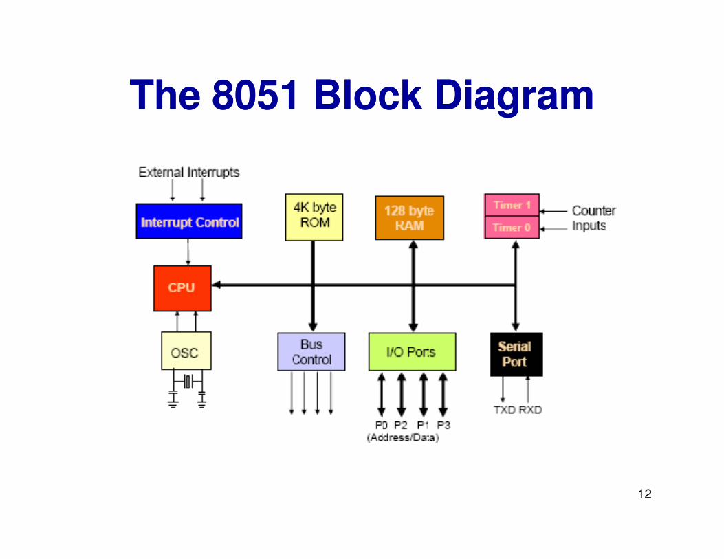
The 8051 Block DiagramThe 8051 Block Diagram
12
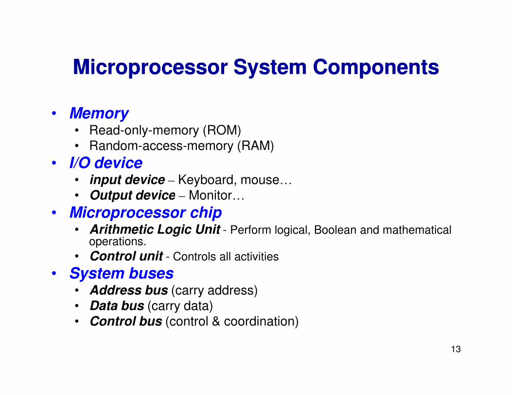
Microprocessor System ComponentsMicroprocessor System Components
• Memory• Read-only-memory (ROM)• Random-access-memory (RAM)
• I/O device• input device – Keyboard, mouse…
• Output device – Monitor…
13
• Output device – Monitor…
• Microprocessor chip• Arithmetic Logic Unit - Perform logical, Boolean and mathematical
operations.
• Control unit - Controls all activities
• System buses• Address bus (carry address)• Data bus (carry data)• Control bus (control & coordination)
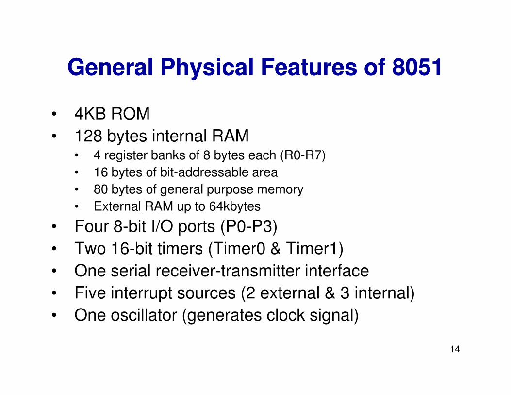
General Physical Features of 8051General Physical Features of 8051
• 4KB ROM
• 128 bytes internal RAM• 4 register banks of 8 bytes each (R0-R7)
• 16 bytes of bit-addressable area
• 80 bytes of general purpose memory
14
• External RAM up to 64kbytes
• Four 8-bit I/O ports (P0-P3)
• Two 16-bit timers (Timer0 & Timer1)
• One serial receiver-transmitter interface
• Five interrupt sources (2 external & 3 internal)
• One oscillator (generates clock signal)
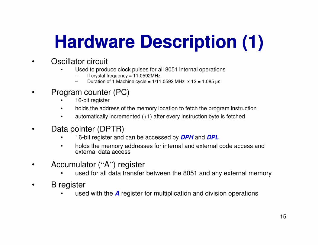
Hardware Description (1)Hardware Description (1)• Oscillator circuit
• Used to produce clock pulses for all 8051 internal operations – If crystal frequency = 11.0592MHz
– Duration of 1 Machine cycle = 1/11.0592 MHz x 12 = 1.085 µs
• Program counter (PC)• 16-bit register
• holds the address of the memory location to fetch the program instruction
• automatically incremented (+1) after every instruction byte is fetched
15
• Data pointer (DPTR) • 16-bit register and can be accessed by DPH and DPL
• holds the memory addresses for internal and external code access and external data access
• Accumulator (“A”) register • used for all data transfer between the 8051 and any external memory
• B register• used with the A register for multiplication and division operations
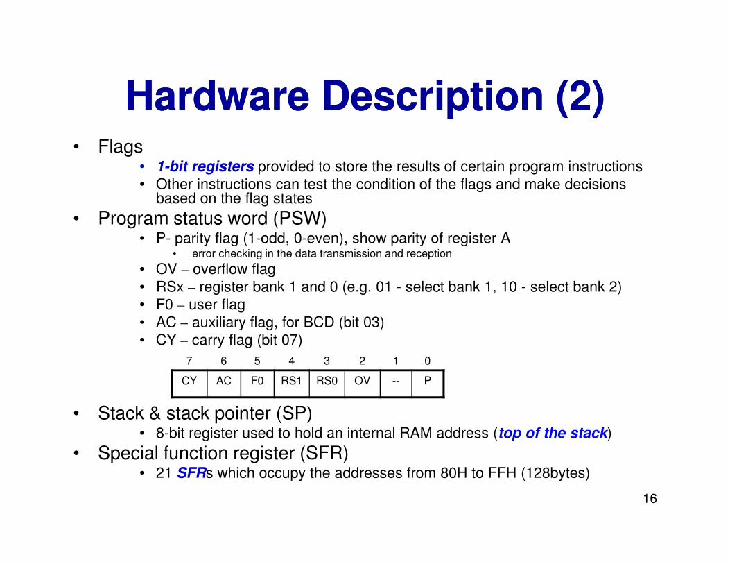
Hardware Description (2)Hardware Description (2)• Flags
• 1-bit registers provided to store the results of certain program instructions
• Other instructions can test the condition of the flags and make decisions based on the flag states
• Program status word (PSW)• P- parity flag (1-odd, 0-even), show parity of register A
• error checking in the data transmission and reception
• OV – overflow flag
• RSx – register bank 1 and 0 (e.g. 01 - select bank 1, 10 - select bank 2)
16
• RSx – register bank 1 and 0 (e.g. 01 - select bank 1, 10 - select bank 2)
• F0 – user flag
• AC – auxiliary flag, for BCD (bit 03)
• CY – carry flag (bit 07)
• Stack & stack pointer (SP) • 8-bit register used to hold an internal RAM address (top of the stack)
• Special function register (SFR)• 21 SFRs which occupy the addresses from 80H to FFH (128bytes)
7 6 5 4 3 2 1 0
CY AC F0 RS1 RS0 OV -- P
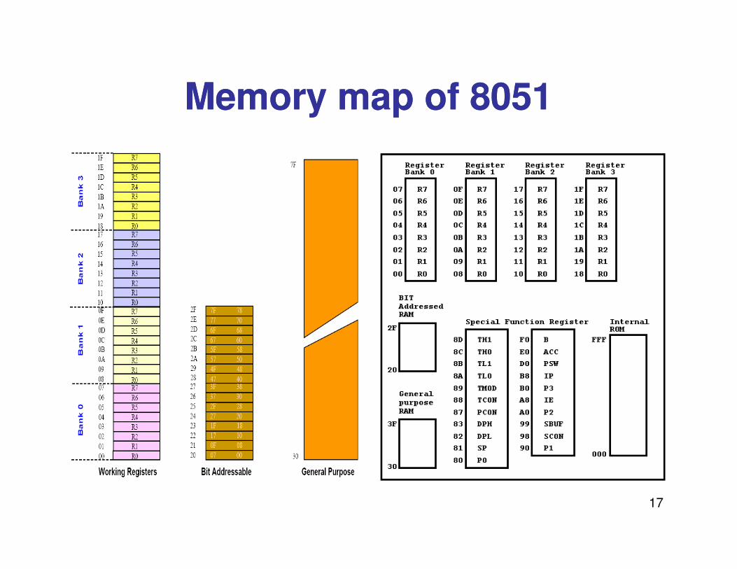
Memory map of 8051 Memory map of 8051
17
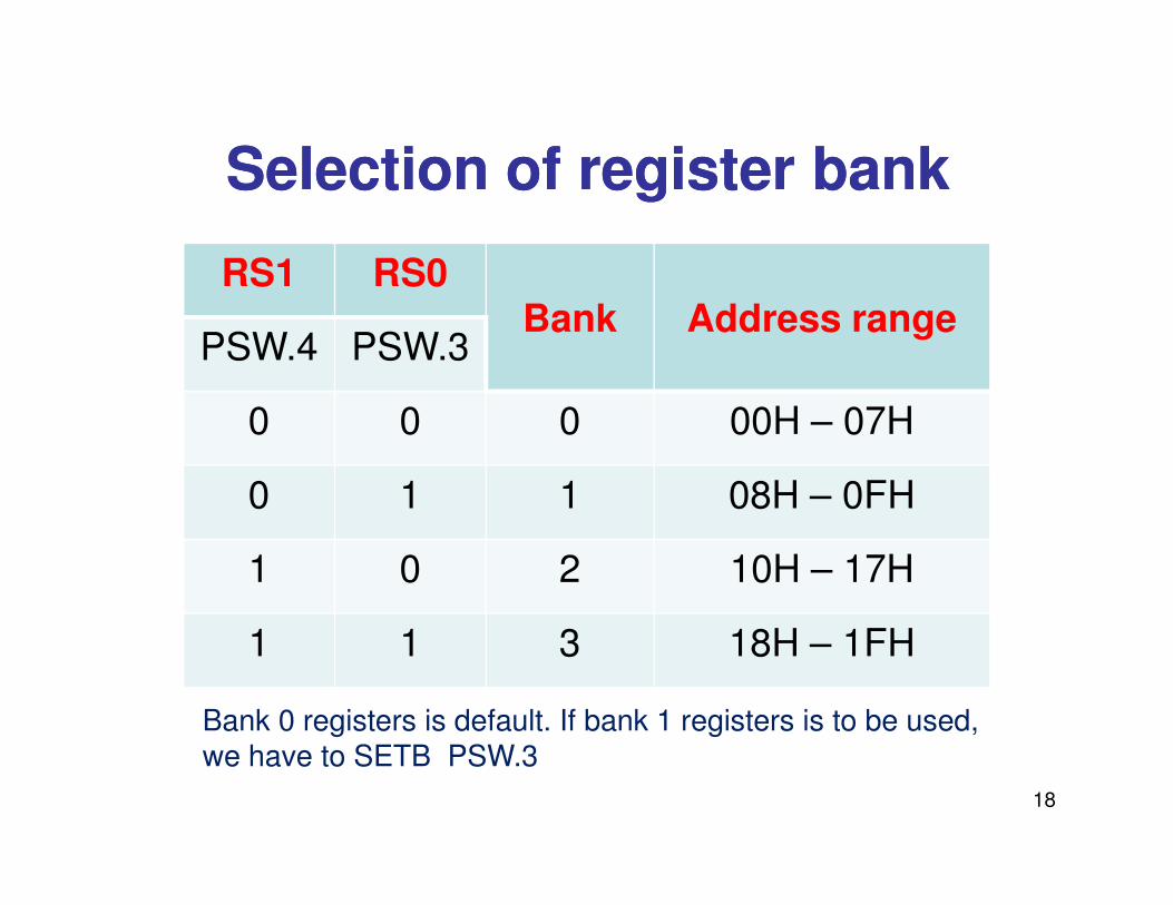
Selection of register bankSelection of register bank
RS1 RS0Bank Address range
PSW.4 PSW.3
0 0 0 00H – 07H
0 1 1 08H – 0FH
1 0 2 10H – 17H
1 1 3 18H – 1FH
18
Bank 0 registers is default. If bank 1 registers is to be used, we have to SETB PSW.3
Stack operation Example 1Stack operation Example 1Show the stack and stack pointer for the following. Assume the default stack area.
MOV R6, #25HMOV R1, #12HMOV R4, #0F3HPUSH 6PUSH 1PUSH 4PUSH 4
0B
0A
09
08
0B
0A
09
08
0B
0A
09
08
0B
0A
09
08
SP = 07
(default)
25
After PUSH 6
SP = 08
12
25
SP = 09
After PUSH 1
F3
12
25
SP = 0A
After PUSH 4
19
Stack operation Example 2Stack operation Example 2
Examine the stack, show the contents of the registers and SP
after execution of the following instruction. All values are in hex.
POP 3 ;POP stack into R3
POP 5 ;POP stack into R5
POP 2 ;POP stack into R2
0B
0A
09
08
0B
0A
09
08
0B
0A
09
08
0B
0A
09
08
Start SP = 0B
54
F9
76
6C
54
F9
76
6C
SP = 0AR3 = 54
After POP 3
54
F9
76
6C
After POP 5
SP = 09R5 = F9
54
F9
76
6C
After POP 2
SP = 08R2 = 76
20
Stack operation Example 3Stack operation Example 3
Show the stack and stack pointer for the following.
MOV SP, #5FH
MOV R2, #25H
MOV R1, #12H
MOV R4, #0F3H
PUSH 2
PUSH 1PUSH 1
PUSH 4
63
62
61
60
63
62
61
60
63
62
61
60
63
62
61
602512
25
F3
12
25
Start SP = 5F SP = 60 SP = 61 SP = 62
After PUSH 2 After PUSH 1 After PUSH 4
21
Syntax = format/rule
[label:] mnemonic [operands] [;comment]
Items in square brackets are optional
Assembly Language SyntaxAssembly Language Syntax
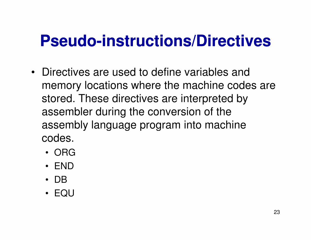
PseudoPseudo--instructions/Directives instructions/Directives
• Directives are used to define variables and
memory locations where the machine codes are
stored. These directives are interpreted by
assembler during the conversion of the
assembly language program into machine
23
assembly language program into machine
codes.
• ORG
• END
• DB
• EQU
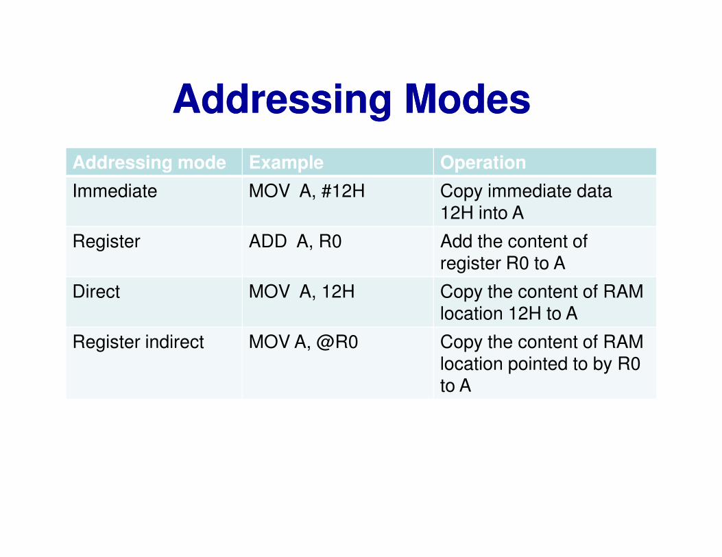
Addressing ModesAddressing Modes
Addressing mode Example Operation
Immediate MOV A, #12H Copy immediate data 12H into A
Register ADD A, R0 Add the content of register R0 to A
Direct MOV A, 12H Copy the content of RAM location 12H to A
Register indirect MOV A, @R0 Copy the content of RAM location pointed to by R0 to A
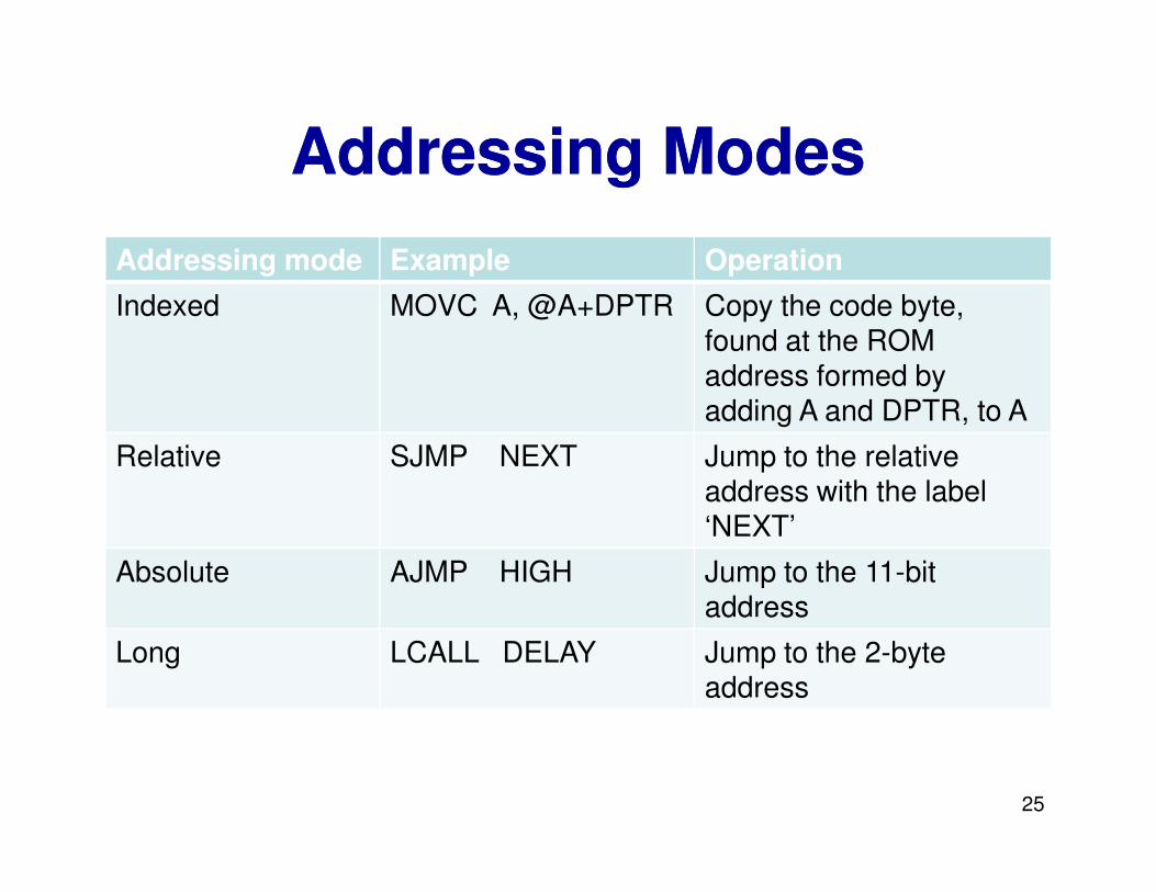
Addressing mode Example Operation
Indexed MOVC A, @A+DPTR Copy the code byte, found at the ROM address formed by adding A and DPTR, to A
Relative SJMP NEXT Jump to the relative
Addressing ModesAddressing Modes
25
Relative SJMP NEXT Jump to the relative address with the label ‘NEXT’
Absolute AJMP HIGH Jump to the 11-bit address
Long LCALL DELAY Jump to the 2-byte address
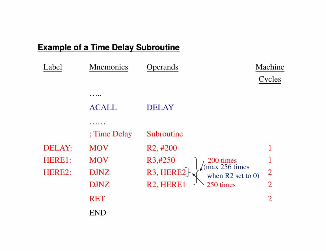
Example of a Time Delay SubroutineExample of a Time Delay Subroutine
Label Mnemonics Operands Machine
Cycles
…..
ACALL DELAY
…………
; Time Delay Subroutine
DELAY: MOV R2, #200 1
HERE1: MOV R3,#250 200 times 1
HERE2: DJNZ R3, HERE2 2
DJNZ R2, HERE1 250 times 2
RET 2
END
(max 256 times
when R2 set to 0)
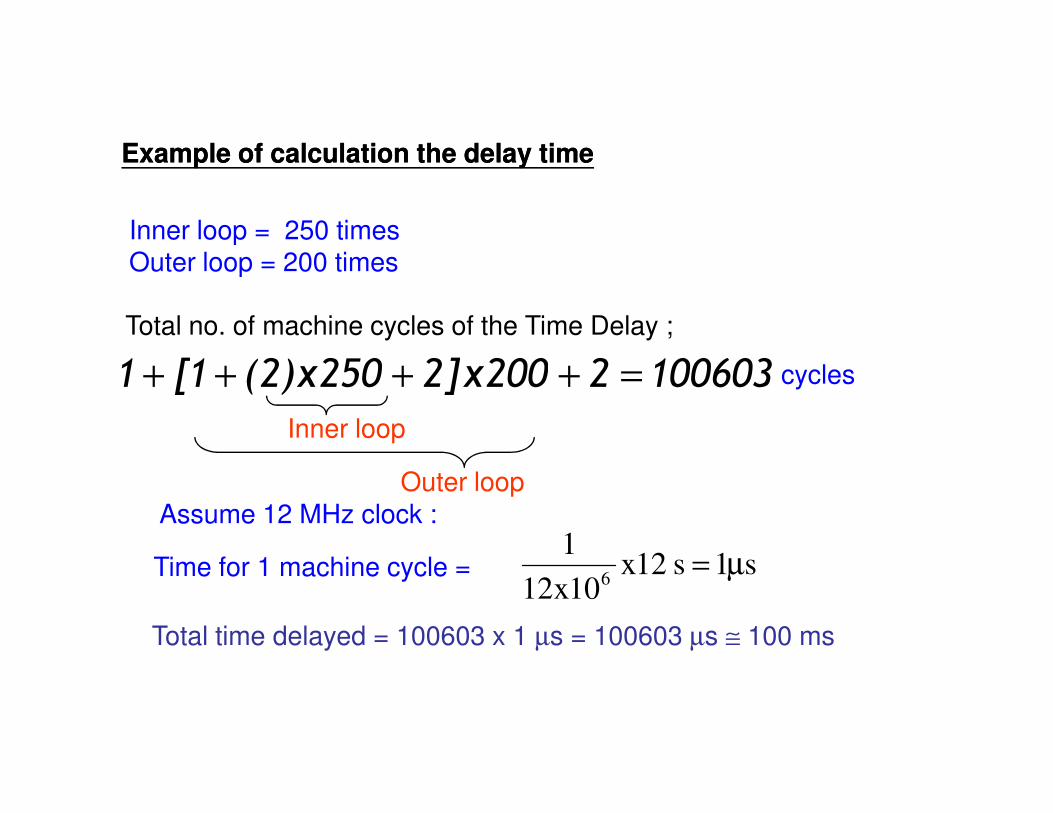
Total no. of machine cycles of the Time Delay ;
1006032200x]2250x)2(1[1 =++++
Example of calculation the delay timeExample of calculation the delay time
Inner loop = 250 timesOuter loop = 200 times
cycles
Time for 1 machine cycle = s1s12x10x12
16
µ=
Total time delayed = 100603 x 1 µs = 100603 µs ≅ 100 ms
Assume 12 MHz clock :
Inner loop
Outer loop
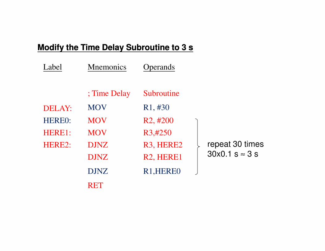
Modify the Time Delay Subroutine to 3 sModify the Time Delay Subroutine to 3 s
Label Mnemonics Operands
; Time Delay Subroutine
DELAY: MOV R1, #30
HERE0: MOV R2, #200
HERE1: MOV R3,#250
HERE2: DJNZ R3, HERE2
DJNZ R2, HERE1
DJNZ R1,HERE0
RET
repeat 30 times 30x0.1 s ≈ 3 s

I/O Ports and interruptsI/O Ports and interrupts
29
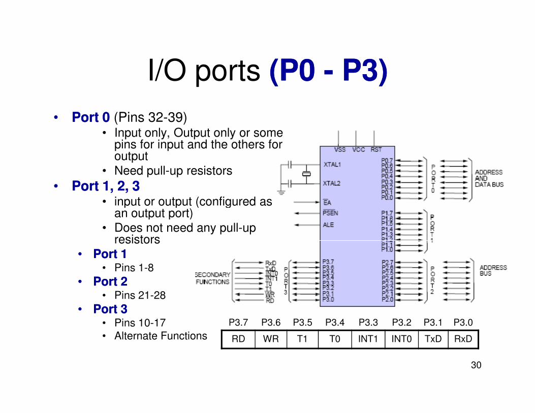
I/O ports (P0 (P0 -- P3)P3)
•• Port 0Port 0 (Pins 32-39)• Input only, Output only or some
pins for input and the others for output
• Need pull-up resistors
•• Port 1, 2, 3Port 1, 2, 3• input or output (configured as
an output port)
30
• input or output (configured as an output port)
• Does not need any pull-up resistors
•• Port 1Port 1• Pins 1-8
•• Port 2 Port 2 • Pins 21-28
•• Port 3 Port 3 • Pins 10-17
• Alternate Functions
P3.7 P3.6 P3.5 P3.4 P3.3 P3.2 P3.1 P3.0
RD WR T1 T0 INT1 INT0 TxD RxD
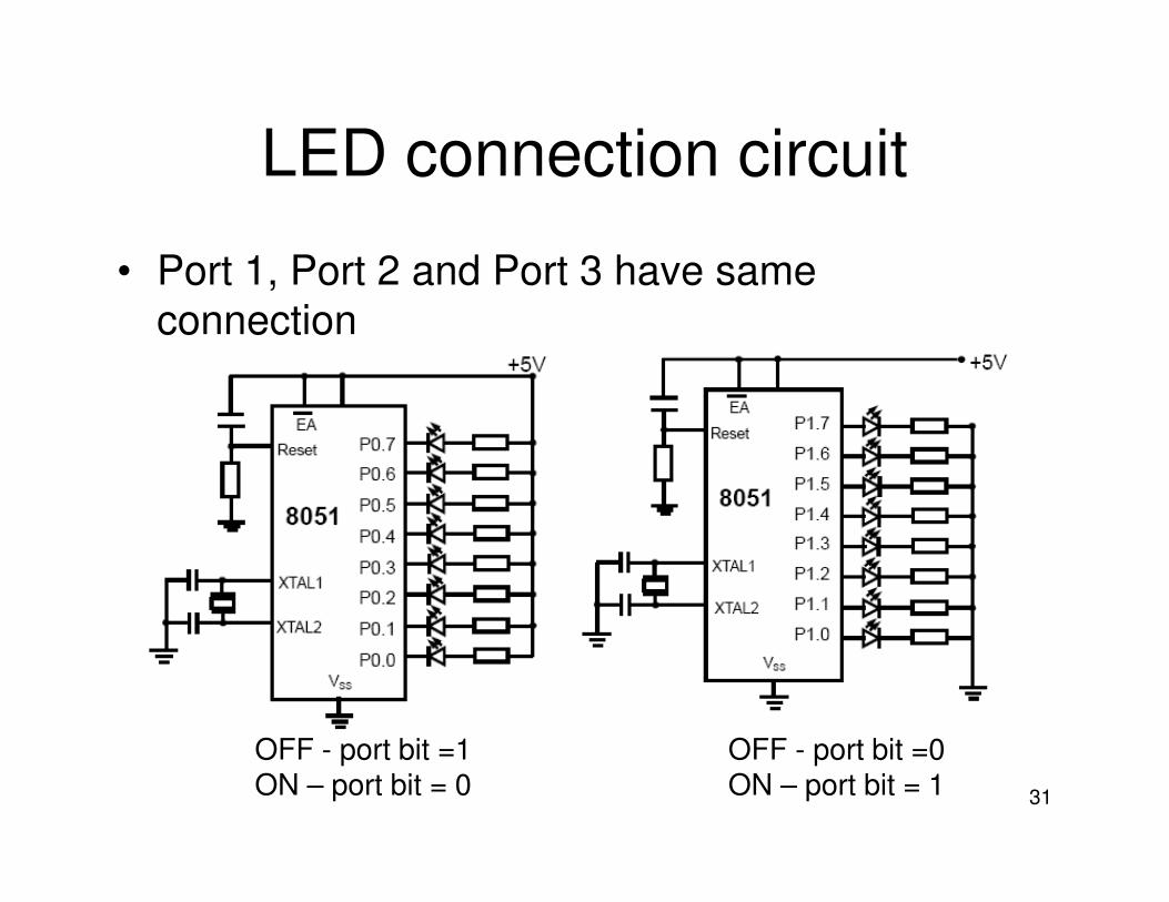
LED connection circuit
• Port 1, Port 2 and Port 3 have same
connection
31
OFF - port bit =1ON – port bit = 0
OFF - port bit =0ON – port bit = 1
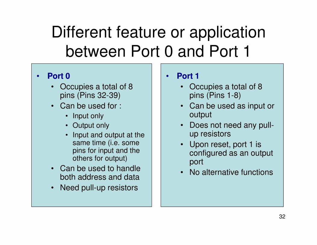
Different feature or application
between Port 0 and Port 1
•• Port 1Port 1
• Occupies a total of 8 pins (Pins 1-8)
• Can be used as input or output
• Does not need any pull-
•• Port 0Port 0
• Occupies a total of 8 pins (Pins 32-39)
• Can be used for :
• Input only
• Output only
32
• Does not need any pull-up resistors
• Upon reset, port 1 is configured as an output port
• No alternative functions
• Output only
• Input and output at the same time (i.e. some pins for input and the others for output)
• Can be used to handle both address and data
• Need pull-up resistors
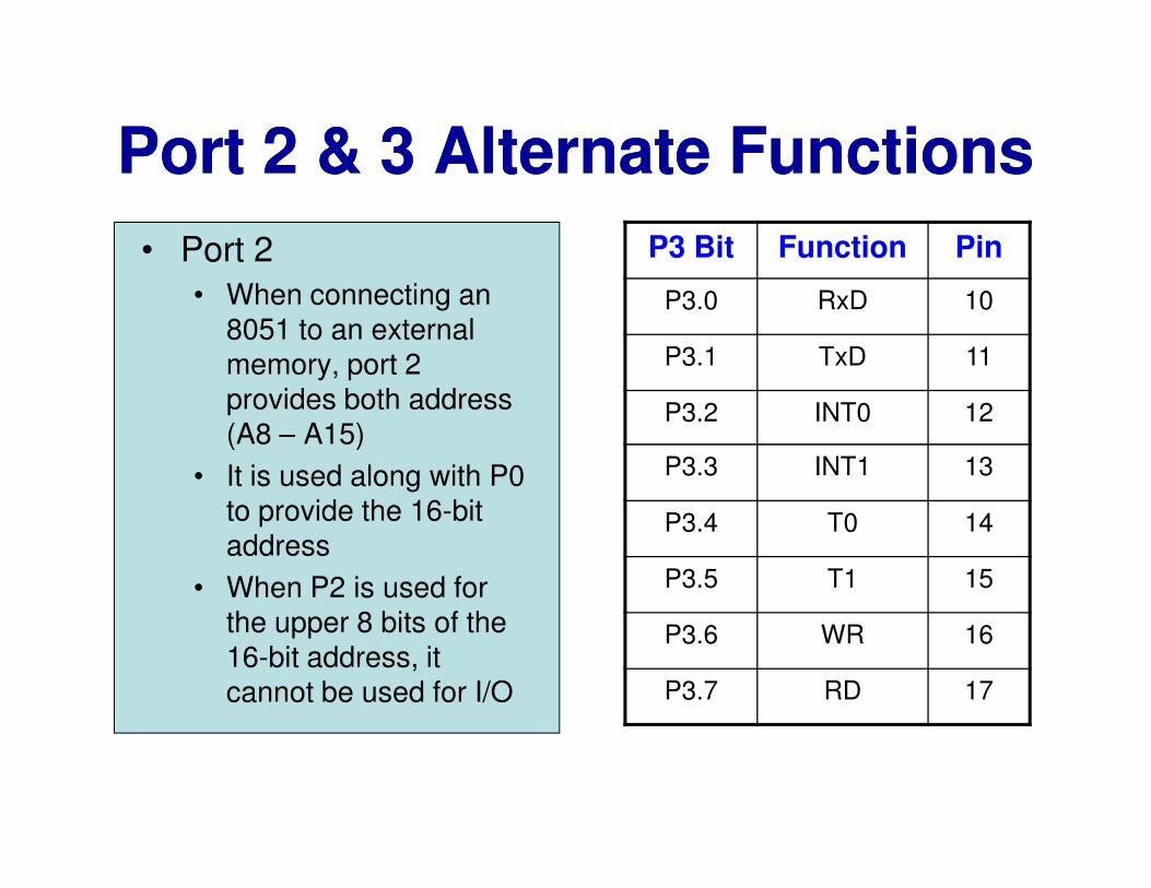
Port 2 & 3 Alternate FunctionsPort 2 & 3 Alternate Functions
P3 Bit Function Pin
P3.0 RxD 10
P3.1 TxD 11
P3.2 INT0 12
• Port 2
• When connecting an 8051 to an external memory, port 2 provides both address (A8 – A15)
P3.3 INT1 13
P3.4 T0 14
P3.5 T1 15
P3.6 WR 16
P3.7 RD 17
(A8 – A15)
• It is used along with P0 to provide the 16-bit address
• When P2 is used for the upper 8 bits of the 16-bit address, it cannot be used for I/O
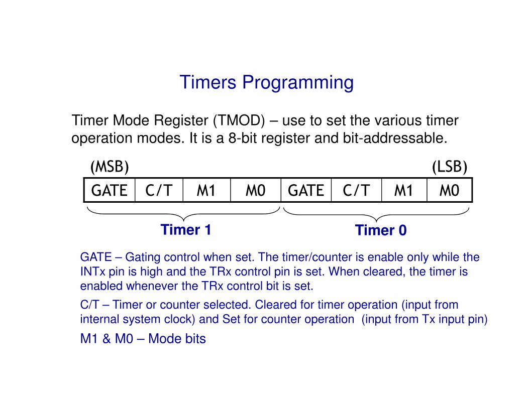
Timers Programming
Timer Mode Register (TMOD) – use to set the various timer
operation modes. It is a 8-bit register and bit-addressable.
(MSB) (LSB)
GATE C/T M1 M0 GATE C/T M1 M0
Timer 1
GATE – Gating control when set. The timer/counter is enable only while the
INTx pin is high and the TRx control pin is set. When cleared, the timer is
enabled whenever the TRx control bit is set.
C/T – Timer or counter selected. Cleared for timer operation (input from
internal system clock) and Set for counter operation (input from Tx input pin)
M1 & M0 – Mode bits
Timer 0
Timers Programming
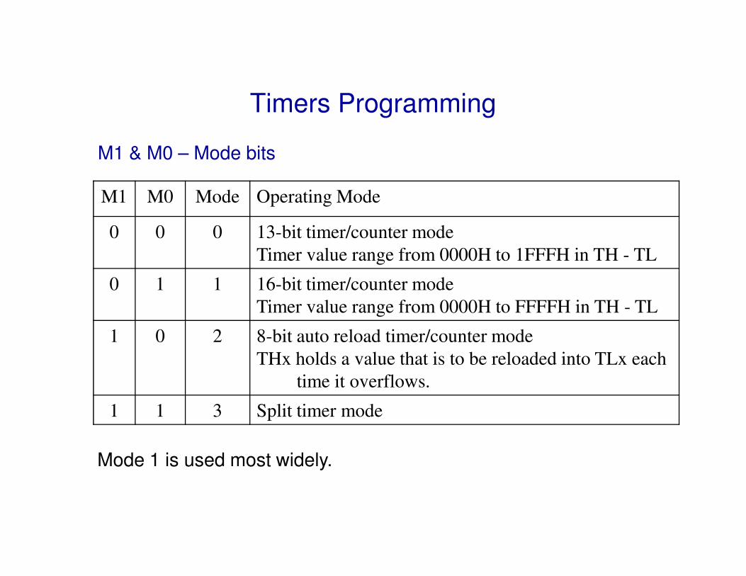
M1 & M0 – Mode bits
M1 M0 Mode Operating Mode
0 0 0 13-bit timer/counter mode
Timer value range from 0000H to 1FFFH in TH - TL
0 1 1 16-bit timer/counter mode0 1 1 16-bit timer/counter mode
Timer value range from 0000H to FFFFH in TH - TL
1 0 2 8-bit auto reload timer/counter mode
THx holds a value that is to be reloaded into TLx each
time it overflows.
1 1 3 Split timer mode
Mode 1 is used most widely.
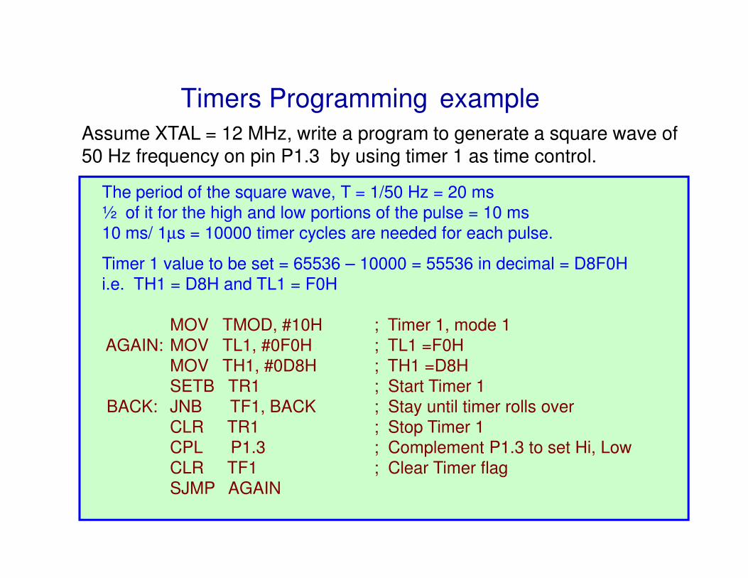
The period of the square wave, T = 1/50 Hz = 20 ms
½ of it for the high and low portions of the pulse = 10 ms
10 ms/ 1µs = 10000 timer cycles are needed for each pulse.
Timer 1 value to be set = 65536 – 10000 = 55536 in decimal = D8F0H
i.e. TH1 = D8H and TL1 = F0H
Assume XTAL = 12 MHz, write a program to generate a square wave of 50 Hz frequency on pin P1.3 by using timer 1 as time control.
Timers Programming example
i.e. TH1 = D8H and TL1 = F0H
MOV TMOD, #10H ; Timer 1, mode 1
AGAIN: MOV TL1, #0F0H ; TL1 =F0H
MOV TH1, #0D8H ; TH1 =D8H
SETB TR1 ; Start Timer 1
BACK: JNB TF1, BACK ; Stay until timer rolls over
CLR TR1 ; Stop Timer 1
CPL P1.3 ; Complement P1.3 to set Hi, Low
CLR TF1 ; Clear Timer flag
SJMP AGAIN
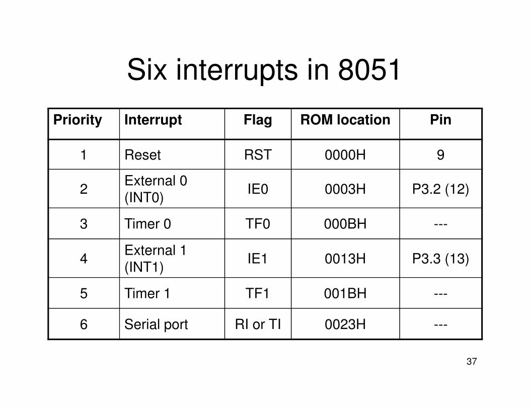
Six interrupts in 8051
Priority Interrupt Flag ROM location Pin
1 Reset RST 0000H 9
2External 0
(INT0)IE0 0003H P3.2 (12)
37
(INT0)
3 Timer 0 TF0 000BH ---
4External 1
(INT1)IE1 0013H P3.3 (13)
5 Timer 1 TF1 001BH ---
6 Serial port RI or TI 0023H ---
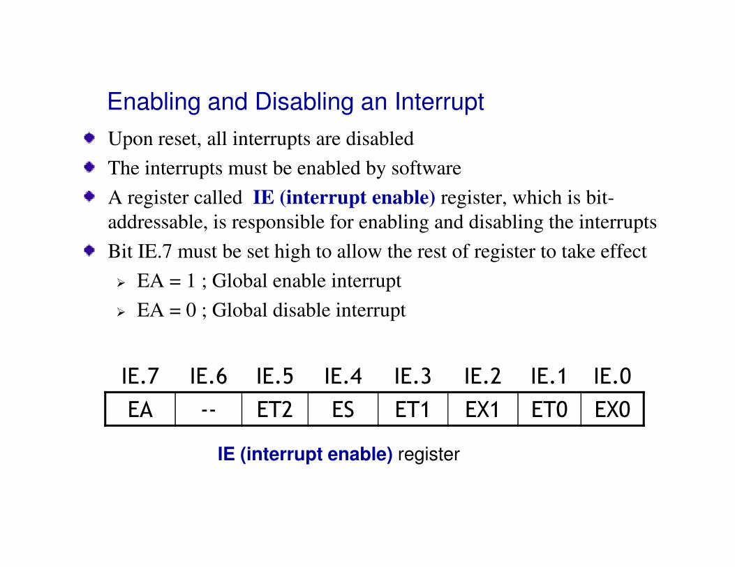
Enabling and Disabling an Interrupt
Upon reset, all interrupts are disabled
The interrupts must be enabled by software
A register called IE (interrupt enable) register, which is bit-
addressable, is responsible for enabling and disabling the interrupts
Bit IE.7 must be set high to allow the rest of register to take effect
� EA = 1 ; Global enable interrupt� EA = 1 ; Global enable interrupt
� EA = 0 ; Global disable interrupt
IE.7 IE.6 IE.5 IE.4 IE.3 IE.2 IE.1 IE.0
EA -- ET2 ES ET1 EX1 ET0 EX0
IE (interrupt enable) register
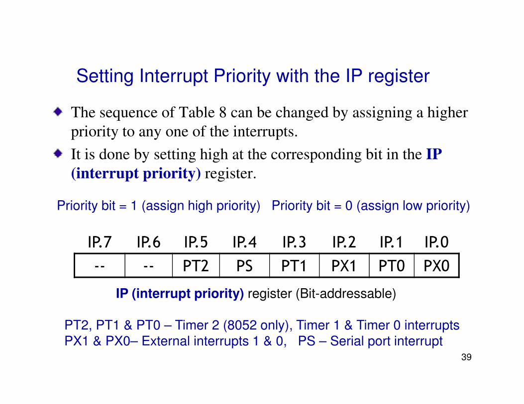
Setting Interrupt Priority with the IP register
The sequence of Table 8 can be changed by assigning a higher
priority to any one of the interrupts.
It is done by setting high at the corresponding bit in the IP
(interrupt priority) register.
Priority bit = 1 (assign high priority) Priority bit = 0 (assign low priority)
39
IP.7 IP.6 IP.5 IP.4 IP.3 IP.2 IP.1 IP.0
-- -- PT2 PS PT1 PX1 PT0 PX0
IP (interrupt priority) register (Bit-addressable)
PT2, PT1 & PT0 – Timer 2 (8052 only), Timer 1 & Timer 0 interruptsPX1 & PX0– External interrupts 1 & 0, PS – Serial port interrupt
Priority bit = 1 (assign high priority) Priority bit = 0 (assign low priority)
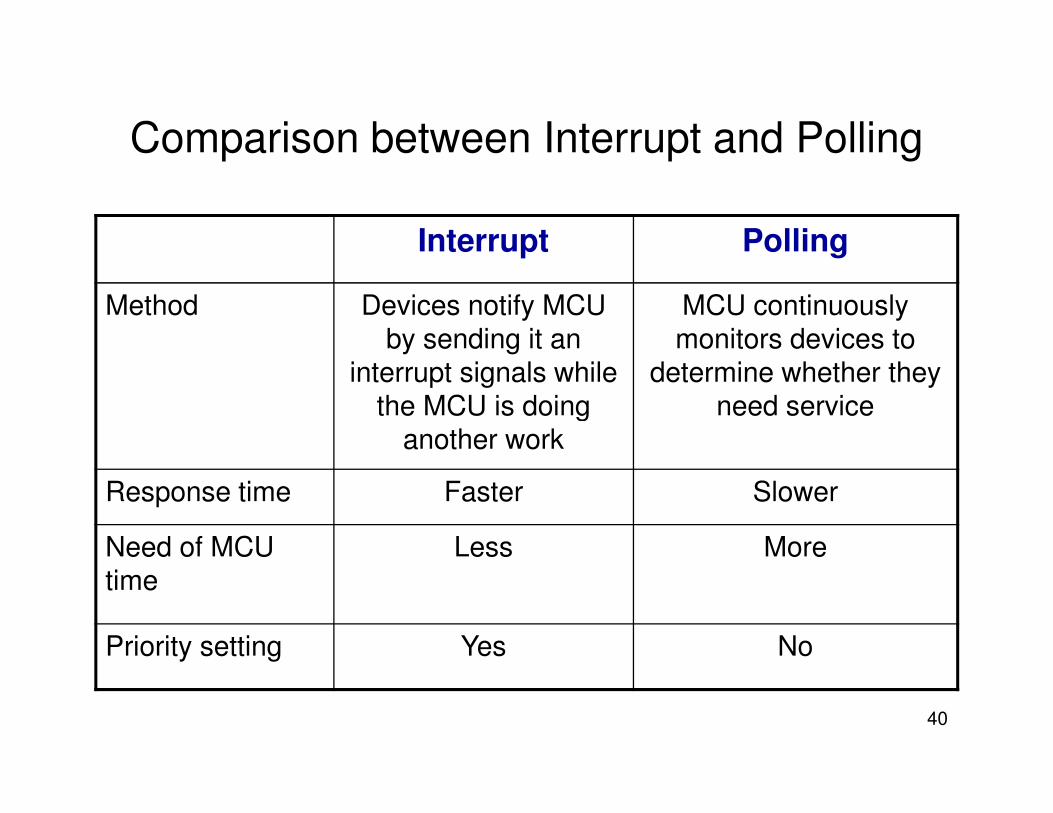
Comparison between Interrupt and Polling
Interrupt Polling
Method Devices notify MCU
by sending it an
interrupt signals while
the MCU is doing
MCU continuously
monitors devices to
determine whether they
need service
40
the MCU is doing
another work
need service
Response time Faster Slower
Need of MCU
time
Less More
Priority setting Yes No

Program ExampleProgram Example
41
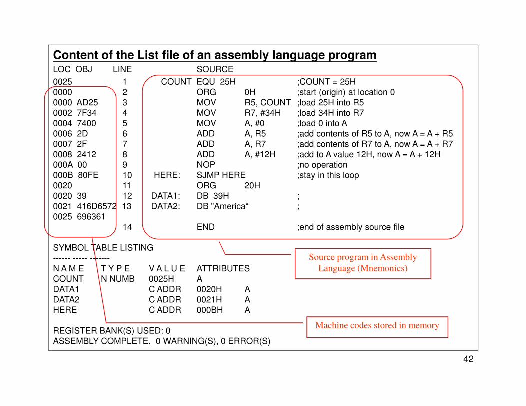
Content of the List file of an assembly language programLOC OBJ LINE SOURCE
0025 1 COUNT EQU 25H ;COUNT = 25H
0000 2 ORG 0H ;start (origin) at location 0
0000 AD25 3 MOV R5, COUNT ;load 25H into R5
0002 7F34 4 MOV R7, #34H ;load 34H into R7
0004 7400 5 MOV A, #0 ;load 0 into A
0006 2D 6 ADD A, R5 ;add contents of R5 to A, now A = A + R5
0007 2F 7 ADD A, R7 ;add contents of R7 to A, now A = A + R7
0008 2412 8 ADD A, #12H ;add to A value 12H, now A = A + 12H
000A 00 9 NOP ;no operation
000B 80FE 10 HERE: SJMP HERE ;stay in this loop
0020 11 ORG 20H
0020 39 12 DATA1: DB 39H ;
0021 416D6572 13 DATA2: DB "America“ ;
42
0021 416D6572 13 DATA2: DB "America“ ;
0025 696361
14 END ;end of assembly source file
SYMBOL TABLE LISTING
------ ----- -------
N A M E T Y P E V A L U E ATTRIBUTES
COUNT N NUMB 0025H A
DATA1 C ADDR 0020H A
DATA2 C ADDR 0021H A
HERE C ADDR 000BH A
REGISTER BANK(S) USED: 0
ASSEMBLY COMPLETE. 0 WARNING(S), 0 ERROR(S)
Machine codes stored in memory
Source program in Assembly
Language (Mnemonics)
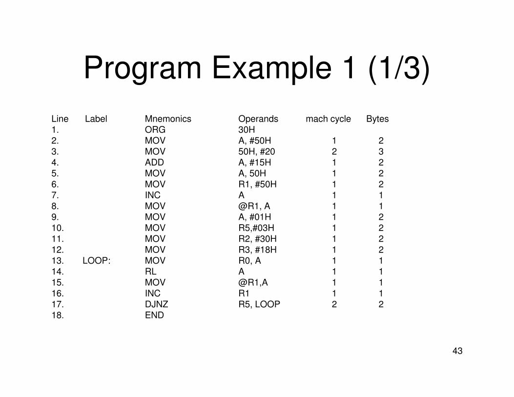
Program Example 1 (1/3)
Line Label Mnemonics Operands mach cycle Bytes1. ORG 30H 2. MOV A, #50H 1 23. MOV 50H, #20 2 34. ADD A, #15H 1 25. MOV A, 50H 1 26. MOV R1, #50H 1 27. INC A 1 1
43
7. INC A 1 18. MOV @R1, A 1 19. MOV A, #01H 1 210. MOV R5,#03H 1 211. MOV R2, #30H 1 212. MOV R3, #18H 1 213. LOOP: MOV R0, A 1 114. RL A 1 115. MOV @R1,A 1 116. INC R1 1 117. DJNZ R5, LOOP 2 218. END
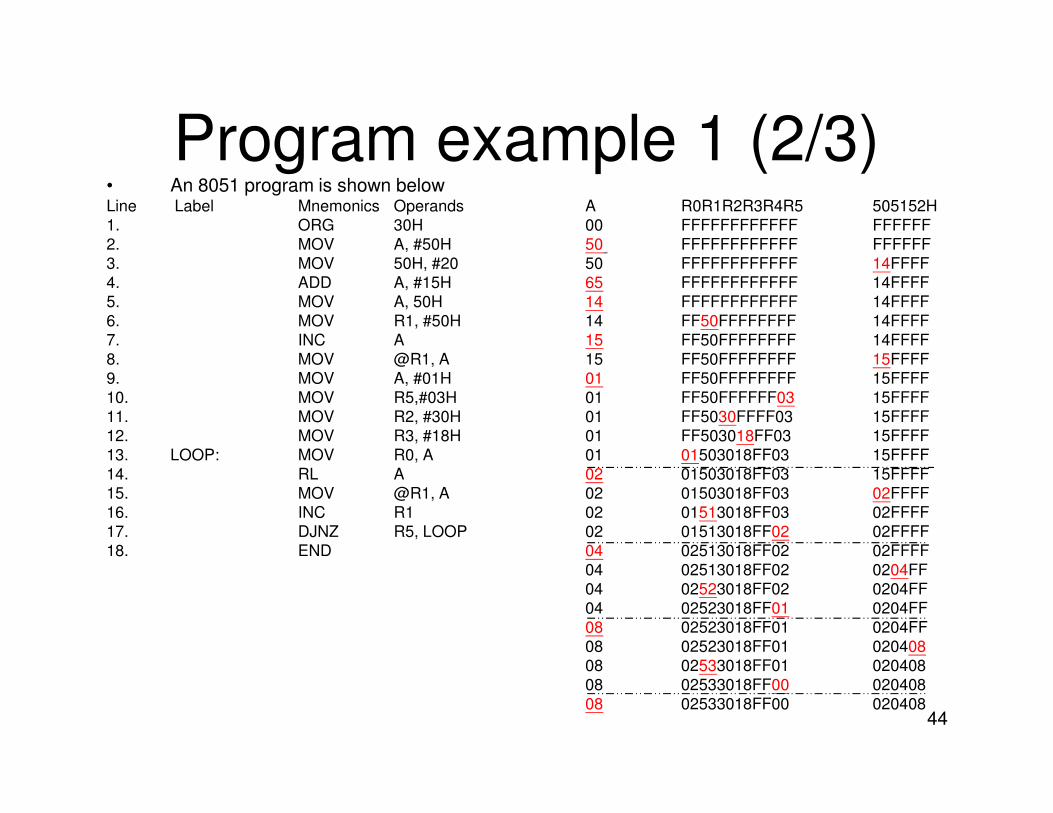
Program example 1 (2/3)• An 8051 program is shown belowLine Label Mnemonics Operands A R0R1R2R3R4R5 505152H
1. ORG 30H 00 FFFFFFFFFFFF FFFFFF
2. MOV A, #50H 50 FFFFFFFFFFFF FFFFFF
3. MOV 50H, #20 50 FFFFFFFFFFFF 14FFFF
4. ADD A, #15H 65 FFFFFFFFFFFF 14FFFF
5. MOV A, 50H 14 FFFFFFFFFFFF 14FFFF
6. MOV R1, #50H 14 FF50FFFFFFFF 14FFFF
7. INC A 15 FF50FFFFFFFF 14FFFF
8. MOV @R1, A 15 FF50FFFFFFFF 15FFFF
9. MOV A, #01H 01 FF50FFFFFFFF 15FFFF
10. MOV R5,#03H 01 FF50FFFFFF03 15FFFF
44
11. MOV R2, #30H 01 FF5030FFFF03 15FFFF
12. MOV R3, #18H 01 FF503018FF03 15FFFF
13. LOOP: MOV R0, A 01 01503018FF03 15FFFF
14. RL A 02 01503018FF03 15FFFF
15. MOV @R1, A 02 01503018FF03 02FFFF
16. INC R1 02 01513018FF03 02FFFF
17. DJNZ R5, LOOP 02 01513018FF02 02FFFF
18. END 04 02513018FF02 02FFFF
04 02513018FF02 0204FF
04 02523018FF02 0204FF
04 02523018FF01 0204FF
08 02523018FF01 0204FF
08 02523018FF01 020408
08 02533018FF01 020408
08 02533018FF00 020408
08 02533018FF00 020408
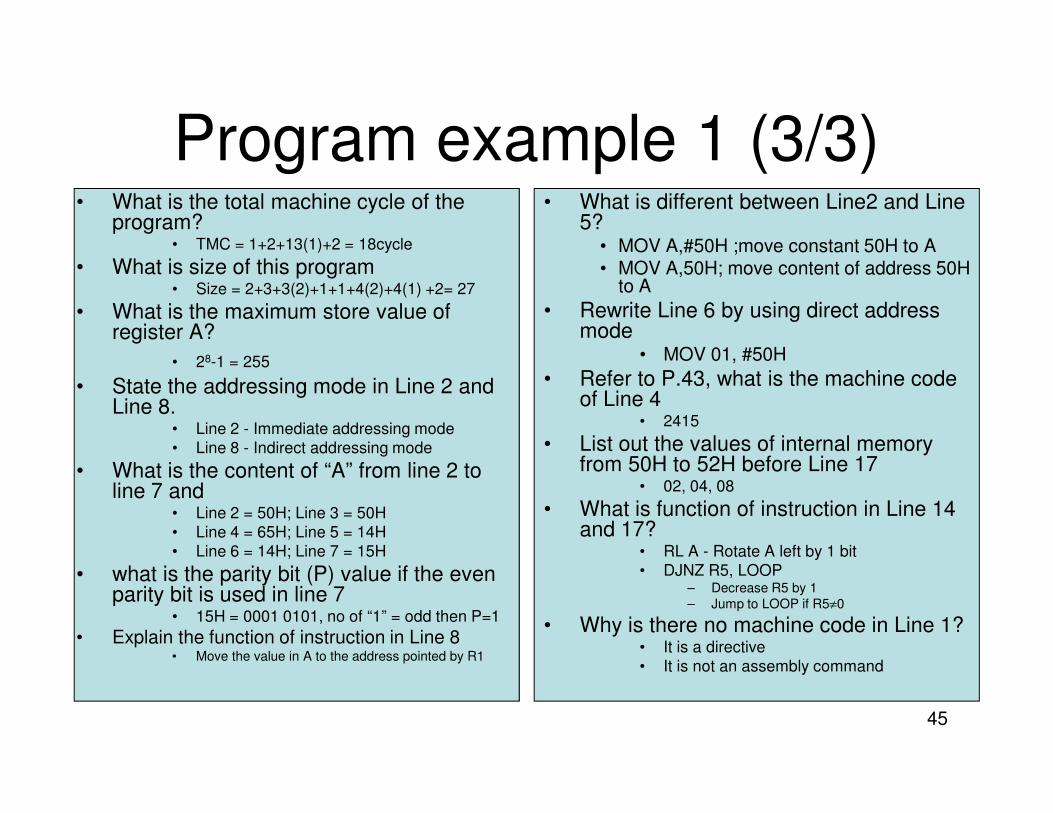
Program example 1 (3/3)• What is the total machine cycle of the
program?• TMC = 1+2+13(1)+2 = 18cycle
• What is size of this program• Size = 2+3+3(2)+1+1+4(2)+4(1) +2= 27
• What is the maximum store value of register A?
• 28-1 = 255
• State the addressing mode in Line 2 and Line 8.
• What is different between Line2 and Line 5?
• MOV A,#50H ;move constant 50H to A• MOV A,50H; move content of address 50H
to A
• Rewrite Line 6 by using direct address mode
• MOV 01, #50H
• Refer to P.43, what is the machine code of Line 4
45
Line 8.• Line 2 - Immediate addressing mode
• Line 8 - Indirect addressing mode
• What is the content of “A” from line 2 to line 7 and
• Line 2 = 50H; Line 3 = 50H
• Line 4 = 65H; Line 5 = 14H
• Line 6 = 14H; Line 7 = 15H
• what is the parity bit (P) value if the even parity bit is used in line 7
• 15H = 0001 0101, no of “1” = odd then P=1
• Explain the function of instruction in Line 8• Move the value in A to the address pointed by R1
of Line 4 • 2415
• List out the values of internal memory from 50H to 52H before Line 17
• 02, 04, 08
• What is function of instruction in Line 14 and 17?
• RL A - Rotate A left by 1 bit
• DJNZ R5, LOOP – Decrease R5 by 1
– Jump to LOOP if R5≠0
• Why is there no machine code in Line 1?• It is a directive
• It is not an assembly command
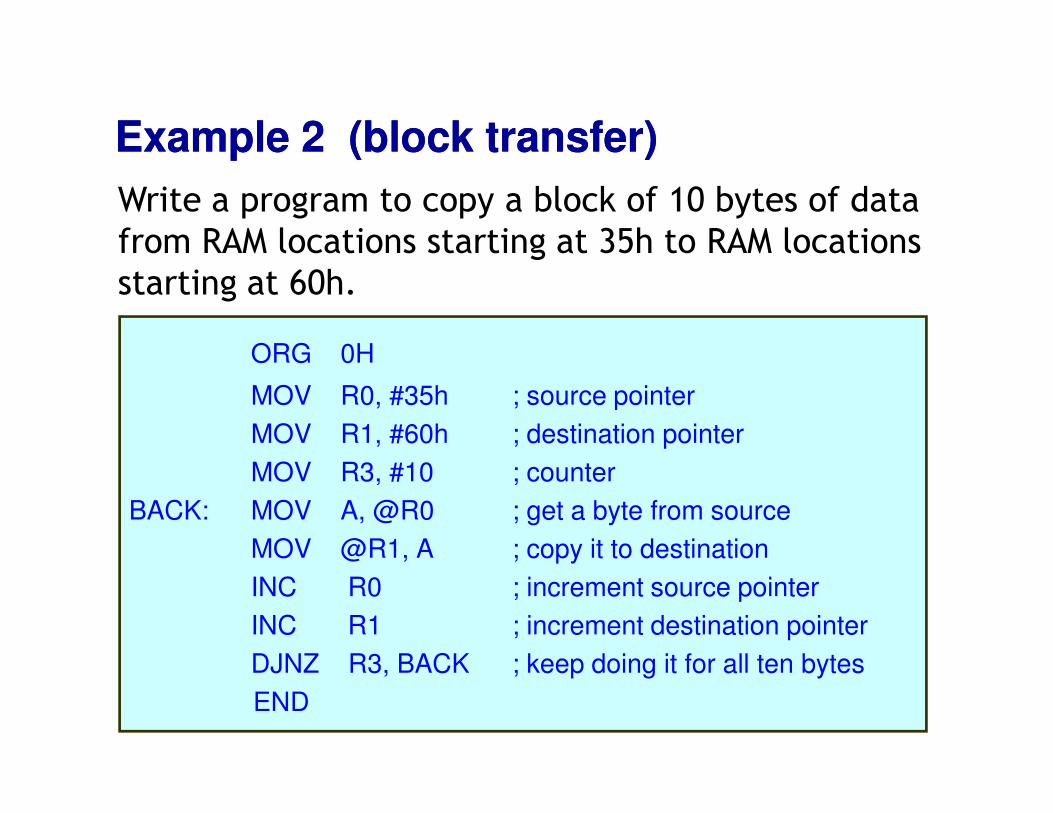
Example 2 (block transfer)Example 2 (block transfer)
Write a program to copy a block of 10 bytes of data
from RAM locations starting at 35h to RAM locations
starting at 60h.
ORG 0H
MOV R0, #35h ; source pointerMOV R0, #35h ; source pointer
MOV R1, #60h ; destination pointer
MOV R3, #10 ; counter
BACK: MOV A, @R0 ; get a byte from source
MOV @R1, A ; copy it to destination
INC R0 ; increment source pointer
INC R1 ; increment destination pointer
DJNZ R3, BACK ; keep doing it for all ten bytes
END
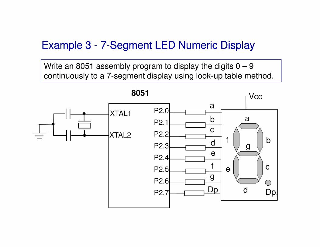
Example 3 Example 3 -- 77--Segment LED Numeric DisplaySegment LED Numeric Display
Write an 8051 assembly program to display the digits 0 – 9 continuously to a 7-segment display using look-up table method.
8051
b
aXTAL1 P2.0
P2.1
Vcc
ab
c
d
e
f
g
XTAL2
P2.1
P2.2
P2.3
P2.4
P2.5
P2.6
P2.7
b
c
d
e
fg
Dp. Dp.
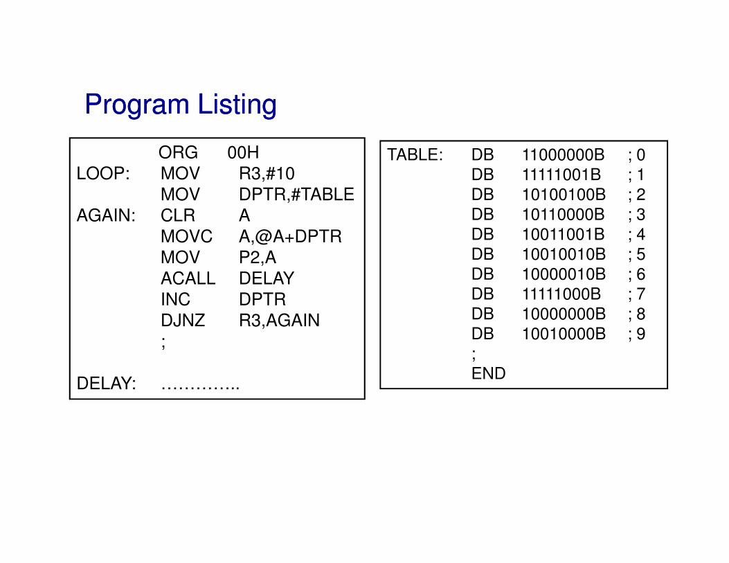
Program Listing Program Listing
ORG 00H
LOOP: MOV R3,#10
MOV DPTR,#TABLE
AGAIN: CLR A
MOVC A,@A+DPTR
MOV P2,A
ACALL DELAY
TABLE: DB 11000000B ; 0
DB 11111001B ; 1
DB 10100100B ; 2
DB 10110000B ; 3
DB 10011001B ; 4
DB 10010010B ; 5
DB 10000010B ; 6ACALL DELAY
INC DPTR
DJNZ R3,AGAIN
;
DELAY: …………..
DB 10000010B ; 6
DB 11111000B ; 7
DB 10000000B ; 8
DB 10010000B ; 9
;
END
AnalogAnalog--toto--digital converter (ADCdigital converter (ADC ))
49
AnalogAnalog--toto--digital converter (ADCdigital converter (ADC ))
AnalogAnalog--toto--digital converter (ADCdigital converter (ADC ))
• The range of an 8-bit ADC is divided into 28 =256 steps (from 0 –255). But there are 255 quantization levels.
• Step size = Vref/(2n-1)
• If the Vref /2 pin of the ADC is open, Vref = VCC
• For Vref = 5 V
nn--bitbit Number of stepsNumber of steps Step Size (mV)Step Size (mV)
50
nn--bitbit Number of stepsNumber of steps Step Size (mV)Step Size (mV)
8 28 = 256 5/255 = 19.61
10 210 = 1024 5/1023 = 4.89
12 212 = 4096 5/4095 = 1.22
16 216 = 65536 5/65535 = 0.076
Ex7
Find the step size of an
8 bit ADC, if Vref = 15V.
Step size = 15/(28-1)
= 58.82mV
ADC0804 ChipADC0804 Chip
• D0 – D7
• D0 – D7 are the digital data output pins.
Dout = Vin /step size
Ex8
(a) Find Dout if the Vin = 3V and step
size = 60mV
Dout = Vin/step size = 3/60m = 50
= 0011001000110010
51
(b) Find Vin, for Dout = 00101100. If
Vref/2 = 8V.
Vref = 2(8) = 16V
Step size =16/(28 -1) = 62.75mV
Vin = (00101100)(62.75m)
= (44)(62.75m) = 2.76V2.76V
The timing diagram of ADC0804The timing diagram of ADC0804
52
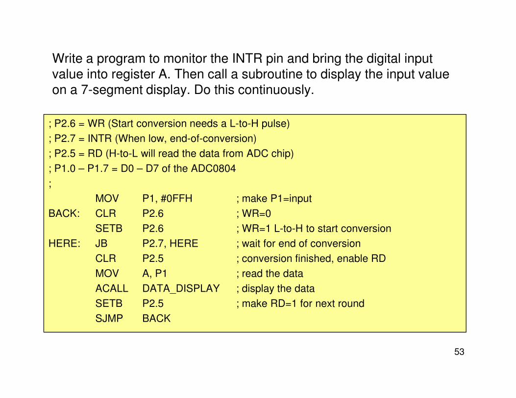
Write a program to monitor the INTR pin and bring the digital input value into register A. Then call a subroutine to display the input value on a 7-segment display. Do this continuously.
; P2.6 = WR (Start conversion needs a L-to-H pulse)
; P2.7 = INTR (When low, end-of-conversion)
; P2.5 = RD (H-to-L will read the data from ADC chip)
; P1.0 – P1.7 = D0 – D7 of the ADC0804
;
MOV P1, #0FFH ; make P1=input
53
MOV P1, #0FFH ; make P1=input
BACK: CLR P2.6 ; WR=0
SETB P2.6 ; WR=1 L-to-H to start conversion
HERE: JB P2.7, HERE ; wait for end of conversion
CLR P2.5 ; conversion finished, enable RD
MOV A, P1 ; read the data
ACALL DATA_DISPLAY ; display the data
SETB P2.5 ; make RD=1 for next round
SJMP BACK
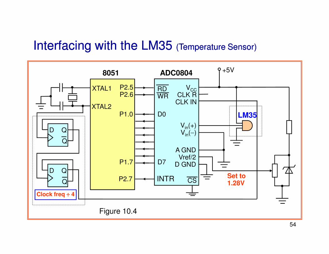
Interfacing with the LM35Interfacing with the LM35 (Temperature Sensor)(Temperature Sensor)
P2.5P2.6
P1.0
RDWR
D0
VCC
CLK RCLK IN
+5V8051 ADC0804
XTAL1
XTAL2
Vin(+)
LM35
D Q
P2.5P2.6
P1.7
P2.7
D7
INTR CS
A GNDVref/2
D GND
Q
Q
D Q
Vin(+)Vin(−)
Set to 1.28V
Clock freq ÷÷÷÷ 4
Q
Q
D Q
Figure 10.4
54
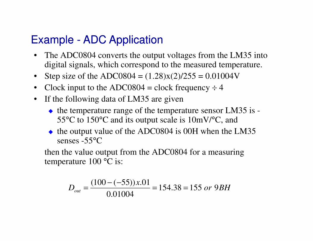
• The ADC0804 converts the output voltages from the LM35 into digital signals, which correspond to the measured temperature.
• Step size of the ADC0804 = (1.28)x(2)/255 = 0.01004V
• Clock input to the ADC0804 = clock frequency ÷ 4
• If the following data of LM35 are given
� the temperature range of the temperature sensor LM35 is -55°C to 150°C and its output scale is 10mV/°C, and
Example Example -- ADC ApplicationADC Application
55°C to 150°C and its output scale is 10mV/°C, and
� the output value of the ADC0804 is 00H when the LM35 senses -55°C
then the value output from the ADC0804 for a measuring temperature 100 °C is:
BHorx
Dout
915538.15401004.0
01.))55(100(==
−−=

Stepper Motor ControlStepper Motor Control
56
Stepper Motor ControlStepper Motor Control
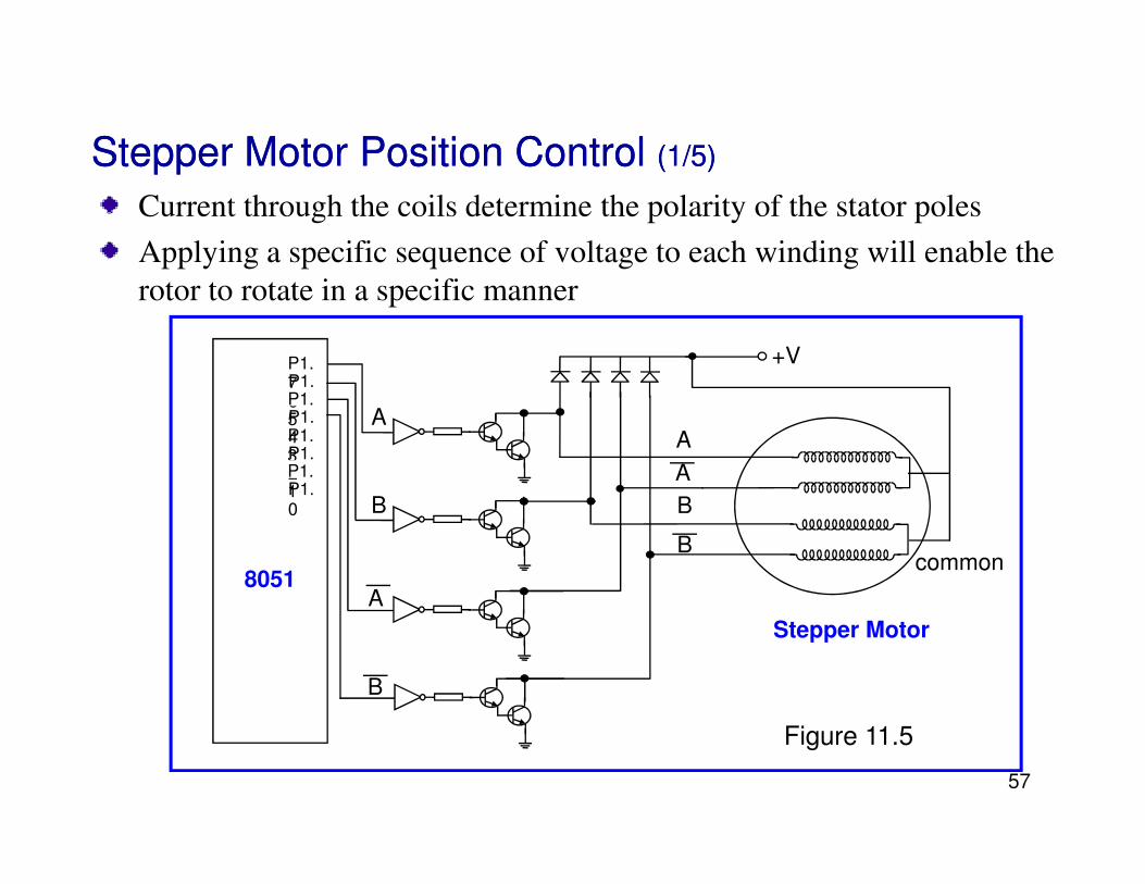
Current through the coils determine the polarity of the stator poles
Applying a specific sequence of voltage to each winding will enable the
rotor to rotate in a specific manner
Stepper Motor Position Control Stepper Motor Position Control (1/5)(1/5)
AA
P1.7P1.6P1.5P1.4P1.
+V
common
A
B
A
BB
B
A
4P1.3P1.2P1.1P1.0
8051
Stepper Motor
Figure 11.5
57
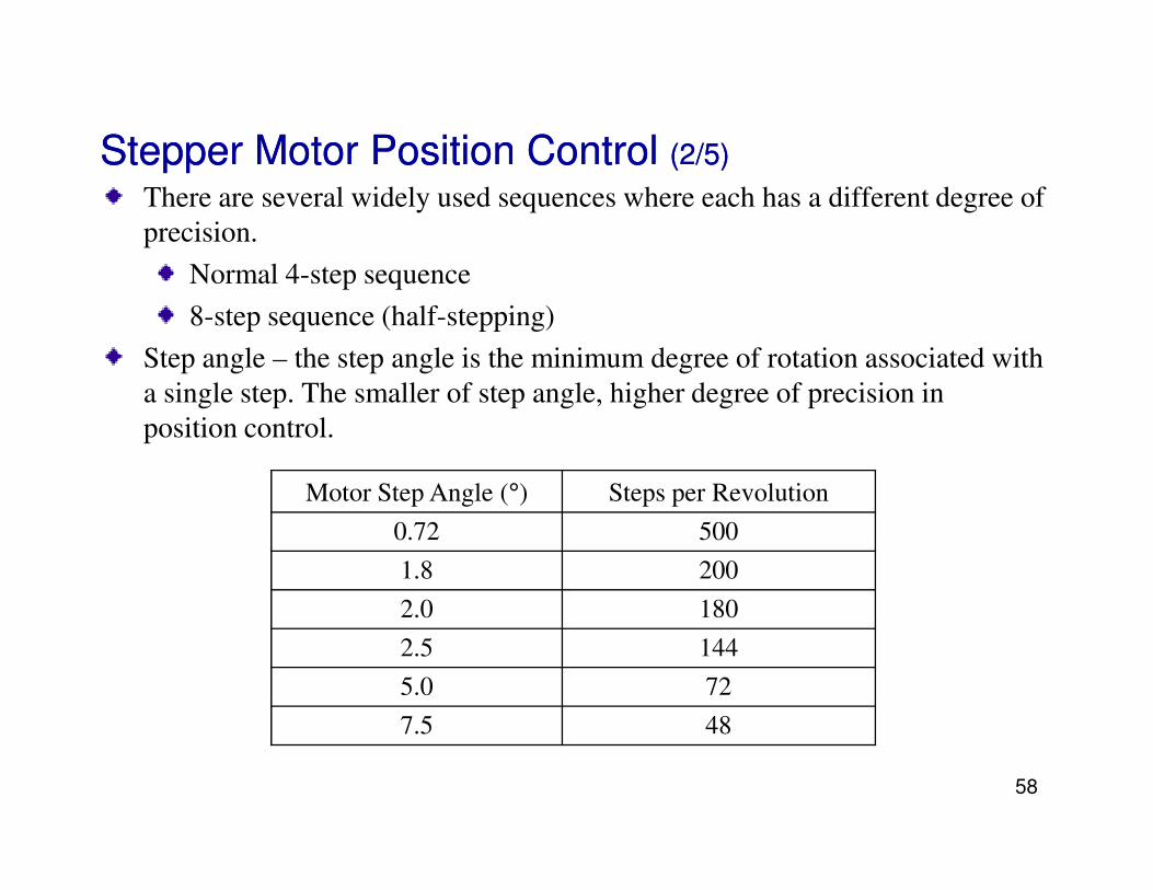
There are several widely used sequences where each has a different degree of
precision.
Normal 4-step sequence
8-step sequence (half-stepping)
Step angle – the step angle is the minimum degree of rotation associated with
a single step. The smaller of step angle, higher degree of precision in
position control.
Stepper Motor Position Control Stepper Motor Position Control (2/5)(2/5)
Motor Step Angle (°) Steps per Revolution
0.72 500
1.8 200
2.0 180
2.5 144
5.0 72
7.5 48
58
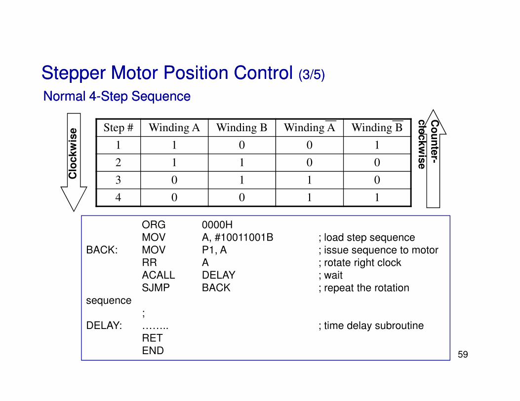
Normal 4Normal 4--Step SequenceStep Sequence
Step # Winding A Winding B Winding A Winding B
1 1 0 0 1
2 1 1 0 0
3 0 1 1 0
4 0 0 1 1
Co
un
ter-
clo
ck
wis
e
Stepper Motor Position Control Stepper Motor Position Control (3/5)(3/5)C
loc
kw
ise
4 0 0 1 1
ORG 0000H
MOV A, #10011001B ; load step sequence
BACK: MOV P1, A ; issue sequence to motor
RR A ; rotate right clock
ACALL DELAY ; wait
SJMP BACK ; repeat the rotation
sequence
;
DELAY: …….. ; time delay subroutine
RET
END 59
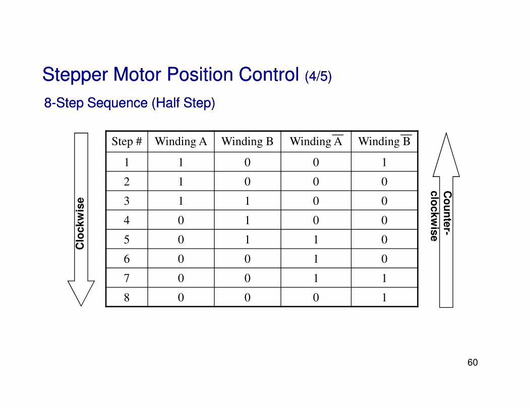
88--Step Sequence (Half Step)Step Sequence (Half Step)
Co
un
ter
clo
ck
wis
e
Stepper Motor Position Control Stepper Motor Position Control (4/5)(4/5)C
loc
kw
ise
Step # Winding A Winding B Winding A Winding B
1 1 0 0 1
2 1 0 0 0
3 1 1 0 0
Co
un
ter-
clo
ck
wis
e
Clo
ck
wis
e 3 1 1 0 0
4 0 1 0 0
5 0 1 1 0
6 0 0 1 0
7 0 0 1 1
8 0 0 0 1
60
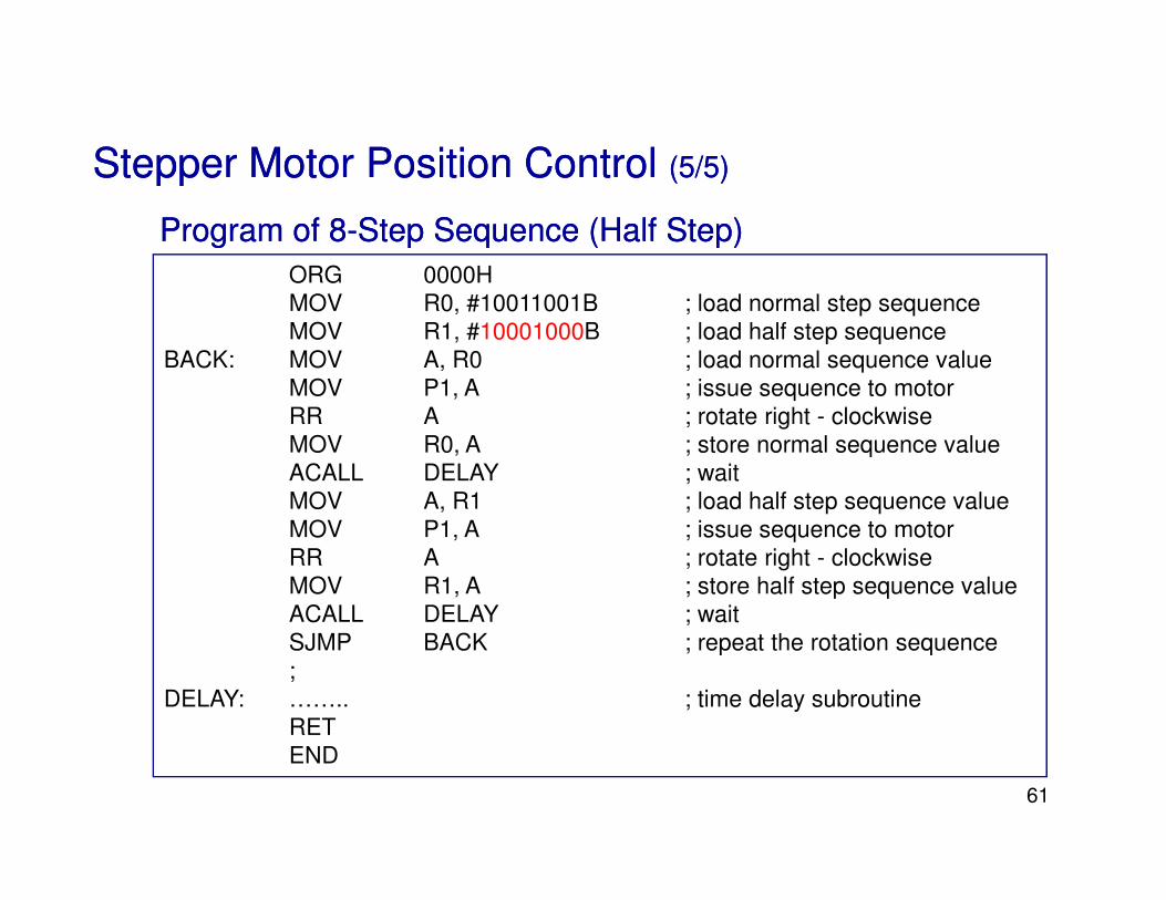
Stepper Motor Position Control Stepper Motor Position Control (5/5)(5/5)
ORG 0000H
MOV R0, #10011001B ; load normal step sequence
MOV R1, #10001000B ; load half step sequence
BACK: MOV A, R0 ; load normal sequence value
MOV P1, A ; issue sequence to motor
RR A ; rotate right - clockwise
MOV R0, A ; store normal sequence value
Program of 8Program of 8--Step Sequence (Half Step)Step Sequence (Half Step)
MOV R0, A ; store normal sequence value
ACALL DELAY ; wait
MOV A, R1 ; load half step sequence value
MOV P1, A ; issue sequence to motor
RR A ; rotate right - clockwise
MOV R1, A ; store half step sequence value
ACALL DELAY ; wait
SJMP BACK ; repeat the rotation sequence
;
DELAY: …….. ; time delay subroutine
RET
END
61


![{p .f9 ·1]](https://img.pdfslide.us/doc/110x75/627ea4fee86082525d56e3ad/p-f9-1.jpg)