Embed Size (px)
Citation preview
1
Microcomputer Architecture
Table of contents
Copy from MTS51-E051101-EC
Page
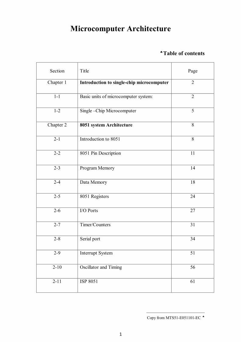
Title
Section
2 Introduction to single-chip microcomputer Chapter 1
2 Basic units of microcomputer system: 1-1
5 Single –Chip Microcomputer 1-2
8 8051 system Architecture Chapter 2
8 Introduction to 8051 2-1
11 8051 Pin Description 2-2
14 Program Memory 2-3
18 Data Memory 2-4
24 8051 Registers 2-5
27 I/O Ports 2-6
31 Timer/Counters 2-7
34 Serial port 2-8
51 Interrupt System 2-9
56 Oscillator and Timing 2-10
61 ISP 8051 2-11
2
Chapter 1
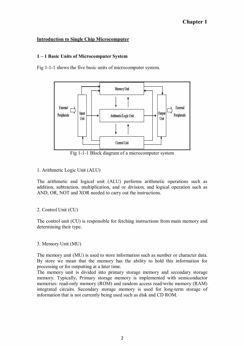
Introduction to Single Chip Microcomputer 1 – 1 Basic Units of Microcomputer System Fig 1-1-1 shows the five basic units of microcomputer system.
InputUnit
OutputUnitArithmetic/Logic Unit
Memory Unit
Control Unit
External
Peripherals
External
PeripheralsInputUnit
OutputUnitArithmetic/Logic Unit
Memory Unit
Control Unit
External
Peripherals
External
Peripherals
Fig 1-1-1 Block diagram of a microcomputer system
1. Arithmetic Logic Unit (ALU) The arithmetic and logical unit (ALU) performs arithmetic operations such as addition, subtraction, multiplication, and or division, and logical operation such as AND, OR, NOT and XOR needed to carry out the instructions. 2. Control Unit (CU) The control unit (CU) is responsible for fetching instructions from main memory and determining their type. 3. Memory Unit (MU) The memory unit (MU) is used to store information such as number or character data. By store we mean that the memory has the ability to hold this information for processing or for outputting at a later time. The memory unit is divided into primary storage memory and secondary storage memory. Typically, Primary storage memory is implemented with semiconductor memories: read-only memory (ROM) and random access read/write memory (RAM) integrated circuits. Secondary storage memory is used for long-term storage of information that is not currently being used such as disk and CD ROM.
3
Semiconductor Memories Rom (Read-Only memory) By using ROM, the information is made nonvolatile; that is, the information is not lost if power is turned off. ROMs can be divided into: 1. Mask ROM Mask ROMs cannot be changed or erased, internationally or otherwise. The data in a mask ROM are inserted during its manufacture, essentially by exposing a photosensitive material through a mask containing the desired bit pattern and then etching away the exposed or unexposed surface. The only way to change the program in a mask ROM is to replace the entire chip. 2. PROM The PROM (Programmable) is like a mask ROM, except that it can be programmed once in the field. 3. EPROM The EPROM (Erasable PROM) cannot only be field – programmed but also field erased. When the quartz window in an EPROM is expressed to storage ultraviolet light for 15-20 minutes, all the bits are sets to 1. If many changes are expected during the design cycle, EPROMs are far more economical than PROMs because they can be reused. 4. EEPROM The EEPROM (Electrically Erasable PROM) or E2PROM can be erased by applying pulses to it instead of requiring it to be put in a special chamber for exposure to ultraviolet light . The new type of ROM called Flash memory is similar to EEPROM in configuration. Flash memory can be programmed on a circuit board by the use of ISP (In-System Programming). RAM (Random access Memory) By using RAM, the information is made volatile; that is, the information is lost if power is turned off. RAMs come in tow varieties: static and dynamic. 1. SRAM SRAMs are constructed internally using circuits similar to the basic D latch. These memories have the property that their continents are retained as long as the power is kept on. 2. DRAM (Dynamic RAM) DRAMs, in contrast, do not use latch – like circuits. Instead, a dynamic RAM is an array of tiny capacitors, each of which can be charged or discharged, allowing 0 and 1 to be stored. Because the electric charge tends to leak out, each bit in a dynamic RAM must be refreshed every few milliseconds to prevent the data from leaking away.
4
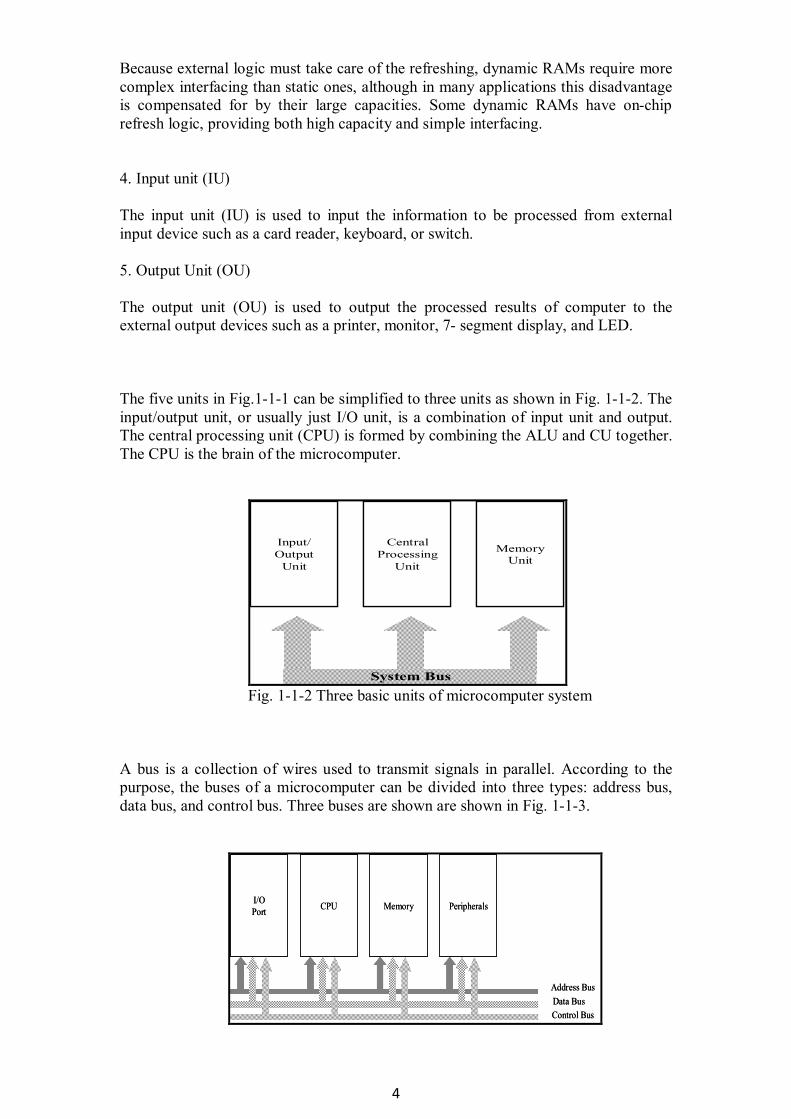
Because external logic must take care of the refreshing, dynamic RAMs require more complex interfacing than static ones, although in many applications this disadvantage is compensated for by their large capacities. Some dynamic RAMs have on-chip refresh logic, providing both high capacity and simple interfacing. 4. Input unit (IU) The input unit (IU) is used to input the information to be processed from external input device such as a card reader, keyboard, or switch. 5. Output Unit (OU) The output unit (OU) is used to output the processed results of computer to the external output devices such as a printer, monitor, 7- segment display, and LED. The five units in Fig.1-1-1 can be simplified to three units as shown in Fig. 1-1-2. The input/output unit, or usually just I/O unit, is a combination of input unit and output. The central processing unit (CPU) is formed by combining the ALU and CU together. The CPU is the brain of the microcomputer.
Input/Output
Unit
CentralProcessing
Unit
MemoryUnit
System Bus
Input/Output
Unit
CentralProcessing
Unit
MemoryUnit
System Bus Fig. 1-1-2 Three basic units of microcomputer system
A bus is a collection of wires used to transmit signals in parallel. According to the purpose, the buses of a microcomputer can be divided into three types: address bus, data bus, and control bus. Three buses are shown are shown in Fig. 1-1-3.
Fig. 1-1-3 System bus of microcomputer system
I/OPort PeripheralsCPU Memory
Address BusData BusControl Bus
I/OPort PeripheralsCPU Memory
Address BusData BusControl Bus
5
1. Address Bus The unidirectional address bus transmits the address signals emitted from CPU to memory and I/O port. 2. Data Bus The signal on the bidirectional data bus is the data either from CPU to memory and I/O or from memory and I/O to CPU. 3. Control Bus The control bus is used to transmit the control signals such as read, write, and interrupt control signal. 1 - 2 Single-Chip Microcomputer Microcomputer control system such as air-conditioner, clothes washer-dryer, and security system, etc, are widely used in our everyday life. How to build up a microcomputer control system? The earlier multi-chip 8088 solutions were initially replaced by highly integrated 8-bit single-chip microcomputer devices such as the 8048 and 8051. These devices were tailored to work best as event controllers. For instance, the 8051 offers one-order-of-magnitude higher performance than the 8088, a more powerful instruction set , and special on-chip function such as ROM, RAM, timer/counters, universal asynchronous receiver/transmitter (UART), programmable parallel I/O ports, DAC, and ADC. Today these types of single-chip microcomputers are also called microcontroller. The microcontrollers are widely used in industrial control systems as shown in Fig. 1-2-1
Fig. 1-2-1 Single-chip microcomputer control system Fig. 1-2-2 shows the architectural structure of a single-chip microcomputer system.
Single-ChipMicrocomputer
Software Instruction
Output Components
InputComponents
Interrupt ControlReset
Vcc
Single-ChipMicrocomputer
Software Instruction
Output Components
InputComponents
Interrupt Control
Single-ChipMicrocomputer
Software Instruction
Output Components
InputComponents
Interrupt ControlReset
Vcc
6
Fig. 1-2-2 Architectural structure of a single-chip microcomputer
1. Clock Generator Single-chip microcomputer is a sequential logic circuit normally driven by a clock generator, a device that emits a periodic sequence of pulses. These pulses define machine cycles. During each machine cycle, some activity occurs, such as the execution of an instruction. 2. CPU The CPU is the brain of the single-chip microcomputer. Its function is to execute programs stored in the program memory by fetching their instructions, examining them, and then executing one after another. The CPU is composed of several distinct parts. The control unit is responsible for fetching instructions from program memory and determining their type. The ALU performs arithmetic and logical operations. 3. Interrupt control Interrupt request signals may come from the on-chip peripheral such as timer/counter or external device such as keyboard. The interrupt control circuit receives these requests and determines which request is acknowledged according to the priority level specified. 4. Data Memory The data memory or RAM is used to store data. A part of on-chip data memory is used to store temporary results and certain control information. This memory consists of a number of registers, each of which has a certain function. 5. Program Memory The program memory or ROM is used to store program instructions. IT is divided into the following categories: PROM, EPROM, EEPROM, and Flash.
Clock generator
CPU
InternalControl
Data Memory(RAM)
Program Memory(ROM)
I/P Port
System Bus
Peripherals____________________
TimerUART
A/D ConverterD/A Converter
.
.
.
.
External Interrupt
External Components
Clock generator
CPU
InternalControl
Data Memory(RAM)
Program Memory(ROM)
I/P Port
System BusSystem Bus
Peripherals____________________
TimerUART
A/D ConverterD/A Converter
.
.
.
.
External Interrupt
External Components
7
6. I/O Port The I/O port is an interface between CPU and external devices such as switches and LEDs. Compared with general-purpose microcomputers, single-chip microcomputers provide more I/O ports and more powerful instructions for I/O handling. The more the I/O ports, the more I/O devices can be connected. 7. On-chip Peripherals On-chip peripheral circuits are a single-chip microcomputer offer various special control functions such as timer/counters. Serial ports, PWM, even ADCs and DACs. In general, the more the on-chip peripheral, the higher the system performance.

8
Chapter 2 8051 System Architecture 2-1 Introduction to 8051 The 8051 is the original chip of MCS-51 family devices which originated from Intel. It evolved from the predecessor single-chip microcomputers 8048 and 8049, and therefore its software is upwardly compatible with these devices. The 8051 is a stand-alone, powerful 8-bit single-chip microcomputer and is commonly used for real-time control applications. Although Intel ceased the manufacture of MCS-51 devices, a wide variety of enhanced products based on the 8051 core is still designed and manufactured by other semiconductor manufactures. These devices, such as Atmel AT89C51 and T89C51RX2 family devices and Philips P89C51RX+, P89C51RX2 and P89C66X family devices, are more powerful and more convenient for control applications. The MTS-51 Microcomputer Trainer is equipped with the Philips P89C51RX+/P89C51RX2 chip for the learning of 8051 core architecture and instructions. According to the type and space of internal program memory, the MCs-51 family devices are divided into the following versions: 1. ROMless version The devices such as 8031 has no internal program memory. External ROMs are required for storing the instruction code. 2. Mask ROM version The code and data in a mask-ROM 8051 are inserted during its manufacture, so that it cannot be changed or erased, intentionally or otherwise. 3. PROM version The PROM-based 8051 also called OTP (One Time Programming) version because its program memory can be programmed once in the field. 4. EPROM version The EPROM-based version is named as 8751. It can not only be field-programmed but also field-erased. During the design cycle, EPROM 8751is far more economical than PROM 8051 because it can be used. 5. 8052 This family devices are based on the 8051 core with twice the memory space and an extra timer/counter. The 8052 family devices include ROMless 8032, PROM 8052, and EPROM 8752.
9
The features of Atmel AT89C51/AT89C52 family include:
1. AT89C51 can replace 8751 and AT89C52 can replace 8752.
2. EEPROM program memory.
3. Operating frequency up to 24MHz twice the conventional 8051.
4. Three programmable lock bits.
5. Output driving capability lower than HMOS-based 8051.
6. 20-pin AT89C2051 and AT89C1051 provide less I/O pins and memory space to
suit for small systems.
Philips P80c51 family products include ROMless devices P80C31/80C32, Mask ROM devices P8C51/52/54/58, OTP devices P87C51/52/54/58, and Flash memory devices P89C51/52/54/58. The operating frequency of these devices can be up to 33 MHz. The device P89C51, C52, C54, and C58 contain 4K, 8K, 16K, and 32K bytes of on-chip ROM and 128, 256, 256, and 256 bytes of on-chip RAM, respectively. The features of Intel 8051 family include:
1. 8-bit CPU optimized for control applications.
2. Extensive Boolean processing (single-bit logic) capabilities.
3. 128 bytes of on-chip RAM (256 bytes for 8052).
4. 4K bytes of on-chip ROM (8K bytes for 8052).
5. 32 bidirectional and individually addressable I/O lines.
6. Two 16-bit timer/counters (three for 8052).
7. Full duplex UART.
8. Two-level priority interrupts.
9. 5 interrupt sources including 2 external interrupts and 3 internal interrupts (UART
and 2 timer/counters); 6 interrupts sources for 8052.
10. 64K program memory address space.
11. 64K data memory address space.
12. On-chip clock oscillator can operate up to 12 MHz.
13. Maximum system memory up to 128KB plus internal data memory.
14. CHMOS devices (80C51BH, 80C31BH, 87C51, 80C52, 80C32, 87C52) have two
programmable power-saving modes: Idle and Power Down modes. In Idle mode, the
CPU is turned off while the RAM and other on-chip peripherals continue operating. In
this mode current draw is reduced to about 15% of the current draw when the device
is fully active. In Power Down mode, all on-chip activities are suspended and on-chip
10
RAM continues to hold its data. In this mode the devices typically draws less than 10
µA.
15. The 8751 and 8752 devices contain program lock bits for securing from software
piracy. When these bits are programmed, the internal program memory cannot be read
out, the device cannot to be further programmed, and it cannot execute external
program memory. Erasing the EPROM array deactivates the lock bits and restores the
device's full functionality. It can then be re-programmed.
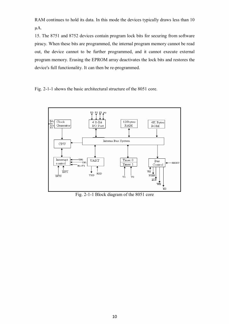
Fig. 2-1-1 shows the basic architectural structure of the 8051 core.
Fig. 2-1-1 Block diagram of the 8051 core
11
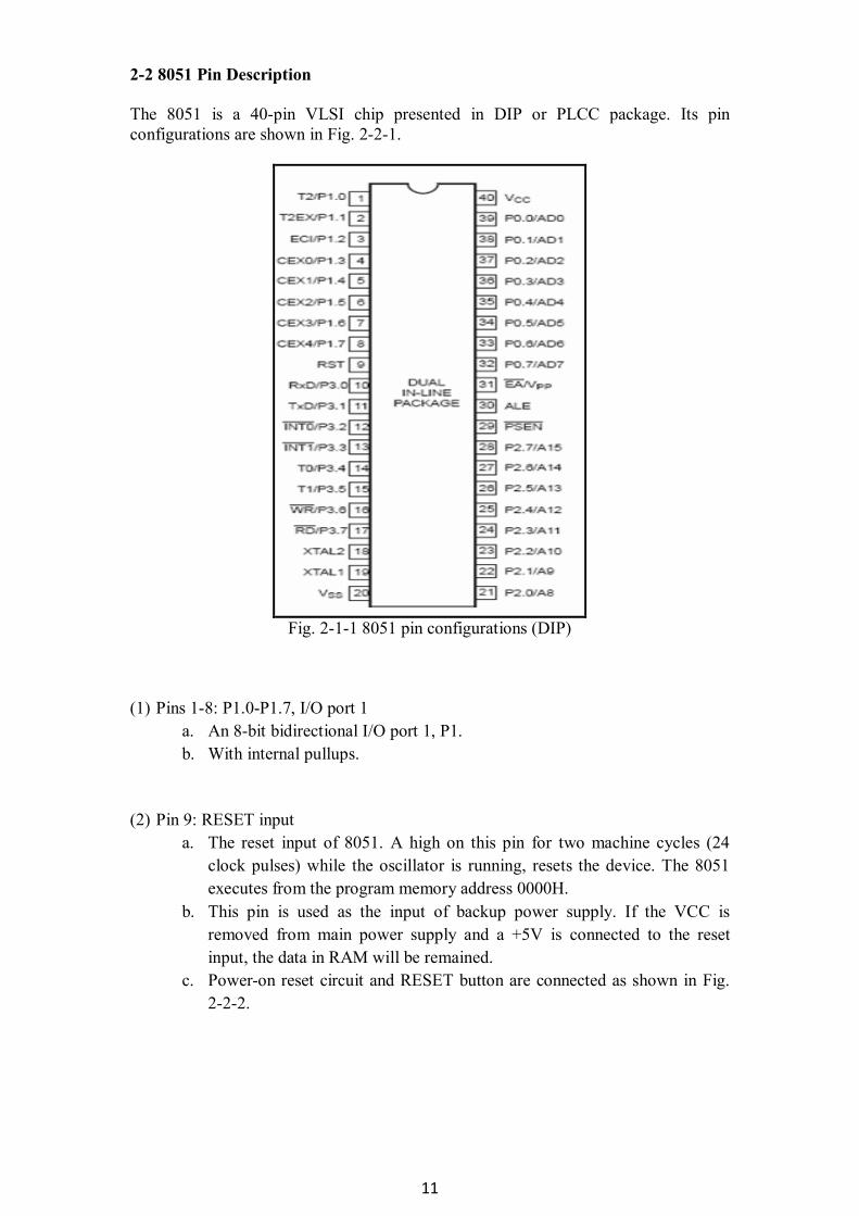
2-2 8051 Pin Description The 8051 is a 40-pin VLSI chip presented in DIP or PLCC package. Its pin configurations are shown in Fig. 2-2-1.
Fig. 2-1-1 8051 pin configurations (DIP)
(1) Pins 1-8: P1.0-P1.7, I/O port 1 a. An 8-bit bidirectional I/O port 1, P1. b. With internal pullups.
(2) Pin 9: RESET input
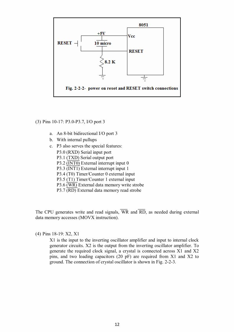
a. The reset input of 8051. A high on this pin for two machine cycles (24 clock pulses) while the oscillator is running, resets the device. The 8051 executes from the program memory address 0000H.
b. This pin is used as the input of backup power supply. If the VCC is removed from main power supply and a +5V is connected to the reset input, the data in RAM will be remained.
c. Power-on reset circuit and RESET button are connected as shown in Fig. 2-2-2.
12
(3) Pins 10-17: P3.0-P3.7, I/O port 3
a. An 8-bit bidirectional I/O port 3 b. With internal pullups c. P3 also serves the special features:
P3.0 (RXD) Serial input port P3.1 (TXD) Serial output port P3.2 (INT0) External interrupt input 0 P3.3 (INT1) External interrupt input 1 P3.4 (T0) Timer/Counter 0 external input P3.5 (T1) Timer/Counter 1 external input P3.6 (WR) External data memory write strobe P3.7 (RD) External data memory read strobe
The CPU generates write and read signals, WR and RD, as needed during external data memory accesses (MOVX instruction). (4) Pins 18-19: X2, X1
X1 is the input to the inverting oscillator amplifier and input to internal clock generator circuits. X2 is the output from the inverting oscillator amplifier. To generate the required clock signal, a crystal is connected across X1 and X2 pins, and two loading capacitors (20 pF) are required from X1 and X2 to ground. The connection of crystal oscillator is shown in Fig. 2-2-3.

13
(5) Pin 20: Vss, ground, 0V reference (6) Pins 21-28: P2.0-P2.7, I/O port 2
a. An 8-bit bidirectional I/O port with internal pull-ups. b. P2 emits the high-order address byte (A8-A15) during fetches from
external program memory and during accesses to external data memory that uses 16-bit addresses (MOVX@DPTR). In this application, it uses strong internal pull-ups when emitting 1s. During accesses to external data memory that uses 8-bit addresses (MOV @ Ri), port 2 emits the contents of the P2 special function register.
(7) Pin 29: PSEN, Program Store Enable a. The read strobe to external program memory. When fetching code from the
external program memory, PSEN is activated each machine cycle, except that two activations are skipped during each access to external data memory. In practice, PSEN pin is wired to the output enable (OE) pin of external ROM.
b. PSEN is not activated during fetches from internal program memory.
(8) Pin 30: ALE/PROG, Address Latch Enable/programming pulse input
a. Output pulse for latching the low byte address (A0-A7) during accesses to external memory.
b. In normal operation, ALE is emitted at a constant rate of 1/6 the oscillator frequency, and can be used for external timing or clocking.
c. In programming 8751, this pin receives the programming pulses.
14
(9) Pin 31: EA /Vpp, External Access Enable/Programming Supply Voltage a. This pin must be externally held low to enable the 8051 to fetch code from
external program memory. For ROMless devices, such as the 8031, this pin should be wired to ground for using external ROM.
b. If EA is held high, the device executes from internal program memory unless the program counter (PC) contains an address greater than the maximum internal program memory space.
c. If the 8051 on-chip program memory is not used, this pin is directly wired to ground.
d. In programming mode, this pin must be connected to the programming power supply generally 12V.
(10) Pins 32-39: P0.0-P0.7, I/O port 0
a. An 8-bit bidirectional I/O port, P0. b. Port 0 is an open-drain configuration. When port 0 serves as an I/O port,
an external pullup resistor (generally 2.2 KΩ) is required for each line. c. Port 0 pins that have 1s written to them float and can be used as high-
impedance inputs. d. Port 0 is also the multiplexed low-order address (A0-A7) and data bus
(D0-D7) during accesses to external program and data memory. In this application, it uses strong internal pull-ups when emitting 1s.
(11) Pin 40: Vcc, positive power supply, +5V. 2-3 Program Memory Program memory is used to store instruction code. The program memory is mask ROM or PROM in the Intel 8051, EPROM in Intel 8751, EEPROM in Atmel AT89C51/52, and Flash in Philips 8051. The 8051 contains 4K-byte internal program memory, 0000H-0FFFH, and is expandable up to 60K bytes of external program memory. Program memory address is determined by the contents of program counter (PC). The map of 8051 program memory is shown in Fig. 2-3-1.
15
In both internal and external ROMs are used, EA pin should be wired to high. When the contents of program counter are less than 4095, the CPU fetches the code stored in internal ROM; otherwise, the CPU fetches the code stored in external ROM. If EA pin is wired to ground, all program fetches are directed to external ROM. The ROMless devices such as 8031 must have this pin externally strapped to ground potential to enable them to execute properly. Mask ROM devices can also be used as ROMless devices 8051 if external ROM is added. External ROM Connection For the expansion of external ROM, pins PSEN, ALE, P0, P2, and an external address latch such as SN74373, should be used. Fig. 2-3-2 shows the connections of expanded 64K and 8K EPROMs. The 74373 contains octal tri-state D latches. During the time that low byte of the program counter is valid on P0, the signal ALE clocks this byte into the address latch 74373. Meanwhile, P2 emits the high byte of the program counter. Then PSEN strobes the EPROM and the code byte is read into the CPU In Fig. 2-3-2 (a) external 64K EPROM is connected so that the EA pin is wired to ground. The EA pin shown in Fig. 2-3-2 (b) is strapped to Vcc for 8K-EPROM expansion, a total of program memory space is therefore 12KB. Since the chip 27512 is a 64 Kbytes EPROM with 16 address lines, therefore both P0 and P2 lines should be used. The 2764 is an 8 Kbytes EPROM with 13 address lines, port 0 lines and P2.0-P2.4 lines are needed.
16
Interrupt Vector Each interrupt is assigned a fixed location in the lower part of the program memory. The interrupt causes the CPU to jump to that location where it commences execution of the service routine. The interrupt service locations are spaced at 8-bytes intervals. If an interrupt service routine is short enough, it can reside entirely within that 8-byte interval. Longer service routines can use a jump instruction to skip over subsequent interrupt locations, if other interrupts are in use. These interrupt service locations are: 1. Memory location 0000H System reset entry. A high on the RESET pin for two machine cycles, the 8051 is reset. After reset, the CPU starts execution from location 0000H. 2. Memory location 0003H Interrupt service location for external interrupt 0. When the INT0 input detects a falling-edge or low-level triggering signal, the CPU fetches opcode from address 0003H.
17
3. Memory location 000BH Interrupt service location for timer/counter 0. When the overflow occurs on the timer/counter 0, the CPU starts execution from location 000BH. 4. Memory location 0013H Interrupt service location for external interrupt 1. When the INT1 input detects a falling-edge or low-level triggering signal, the CPU fetches opcode from address 0013H. 5. Memory location 001BH Interrupt service location for timer/counter 1. When the overflow occurs on the timer/counter 1, the CPU starts execution from location 001BH. 6. Memory location 0023H Interrupt service location for serial port. When 8051 serial port completes transmit or receive, an interrupt request is occurred and the CPU starts from location 0023H if the request is acknowledged. 7. Memory location 002BH Interrupt service location for 8052 timer/counter 2. When the overflow on the timer/counter 2, the CPU starts execution from location 002BH.
An execution of 8051 assembly code with interrupt service routines is shown below.
ORG 000H ; RESET entry JMP MAIN ; jump to main program ORG 003H ; INT0 entry JMP INT0SUB ; jump to INT0 interrupt service routine ORG 00BH ; TIMER0 entry JMP TIM0SUB ; jump to TIMER0 interrupt service
routine ORG 100H ; starting address MAIN: …………………… ; main program …………………… …………………… INTOSUB: …………………… ; INT0 interrupt service routine …………………… …………………… RETI TIM0SUB: …………………… ; TIMER0 interrupt service routine …………………… …………………… RETI END
18
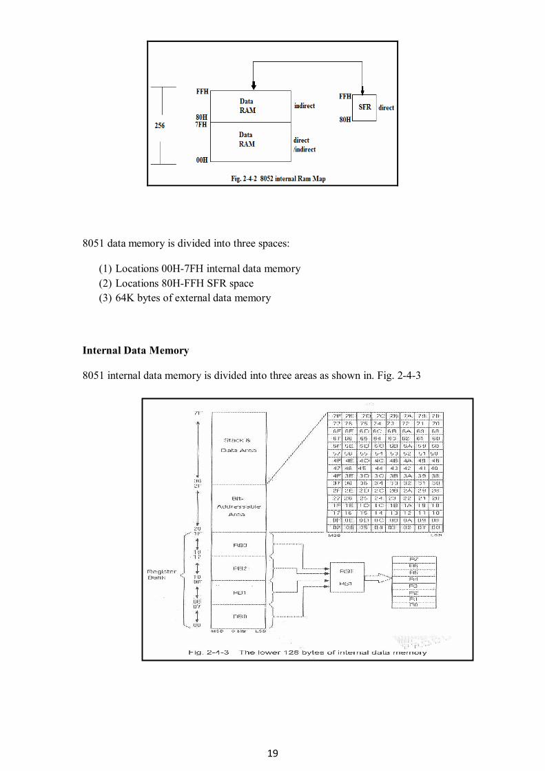
2-4 Data Memory The 8051 contains 128 bytes of on-chip (internal) RAM, locations 00H-7FH, accessible by direct and indirect addressing. This block of internal RAM is used for data, stack, and registers. In fact, 8051 has 256 bytes of on-chip data memory space. A block of 128 bytes, 80H-FFH, is used as the Special Function Registers (SFRs) such as accumulator, stack pointer, timer registers, etc. This block is accessed by direct addressing. The 8052 has 384 bytes of on-chip memory space, that is, 256 bytes of data RAM plus 128 bytes of SFR. The data memory is expandable up to 64K bytes of external data memory. The 8051 treats internal RAM and external RAM as two physically separate blocks and accesses them by different instructions. The internal RAM is accessed by the MOV instruction, whereas the external RAM is accessed by the MOVX instruction. The maximum RAM space of 8051 system is equal to 64K plus 128 bytes. Fig. 2-4-1 shows the 8051 data memory map.
The 8052 has 256 bytes of internal RAM mapped in Fig. 2-4-2. The upper 128 bytes and SFR space occupy the same block of memory addresses, 80H through FFH, although they are physically separate entities. Direct addresses higher than 7FH access the memory space of SFR, and indirect addresses higher than 7FH access a different memory space, data RAM.
19
8051 data memory is divided into three spaces:
(1) Locations 00H-7FH internal data memory (2) Locations 80H-FFH SFR space (3) 64K bytes of external data memory
Internal Data Memory 8051 internal data memory is divided into three areas as shown in. Fig. 2-4-3

20
1. Locations 00H-1FH: Register banks 0-3 The lowest 32 bytes of RAM are grouped into 4 banks of 8 registers. Program instructions call out these registers as R0 through R7. These 4 register banks are referred to as RB0 through RB3. Two bits, RS0 and RS1, in the program status word (PSW) register select which register bank is in use as shown in Table 2-4-1. This allows more efficient use of code space, since register instructions are shorter than the instructions that use direct addressing. Table 2-4-1 Register bank selection
RS1 RS0 Register Bank 0 0 RB0 0 1 RB1 1 0 RB2 1 1 RB3
Any register name in register instructions is actually an address of the 32-byte RAM as shown in Table 2-4-2. If RB2 is selected, for example, then the R3 register represents the address 13H. After reset, the register bank 0, RB0, is default. Table 2-4-2 Register addresses in different register banks Reg. bank Reg. name
RBb0 RB1 RB2 RB3
R0 00H 08H 10H 18H R1 01H 09H 11H 19H R2 02H 0AH 12H 1AH R3 03H 0BH 13H 1BH R4 04H 0CH 14H 1CH R5 05H 0DH 15H 1DH R6 06H 0EH 16H 1EH R7 07H 0FH 17H 1FH 2. Locations 20H-2FH: Bit addressable area Sixteen bytes have been assigned for this area, 20H-2FH. Each of the 16 bytes in this segment can be addressed as a byte. Each one of the 128 bits of this area can also be directly addressed (00H-7FH). The bits can be referred to in two ways both of which are acceptable by the 8051. One way is to refer to their addresses, 00H to 7FH, as shown in Fig. 2-4-3. The other way is with reference to bytes 20H to 2FH. Thus, bits 0-7 can also be referred to as bits 20.0H-20.7H, and bits 8-FH are the same as 21.0H-21.7H and so on. The bit address is calculated by the following equation:
21
[(address – 20H) x8+bit]16 For instance, the bit address of bit 5 at address 24H is equal to (24H – 20H) x8+5= 37=(25)16 And the result is 25H. The results of data byte move and data bit move instructions are different. The instruction
MOV 20H, #00H Clears all the 8 bits of RAM locations 20H, whereas the instruction SETB 20.3H Sets the bit 3 of RAM location 20H.
3. Locations 30H-7FH: Scratch pad area The bytes 30H through 7FH are available to the user as data RAM. However, if the stack pointer has been initialized to this area, enough number of bytes should be left aside to prevent SP data destruction. The first-in-last-out (FILO) stack is used to save the contents of certain registers or some their main program parameters after the context switch to a subroutine. These values are saved by the execution of the PUSH instruction to push them onto the stack. The starting address of the stack is determined by the stack pointer (SP) which increments before value is stored during PUSH and CALL executions. Before a return to the main program takes place, the saved registers and main program parameters are restored. This is done by poping (POP instruction) the values from the stack back into their original locations. The stack pointer decrements after the POP instruction. For example, the instruction
MO V SP, #3FH
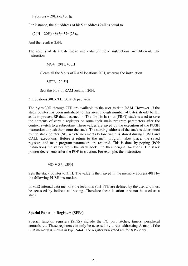
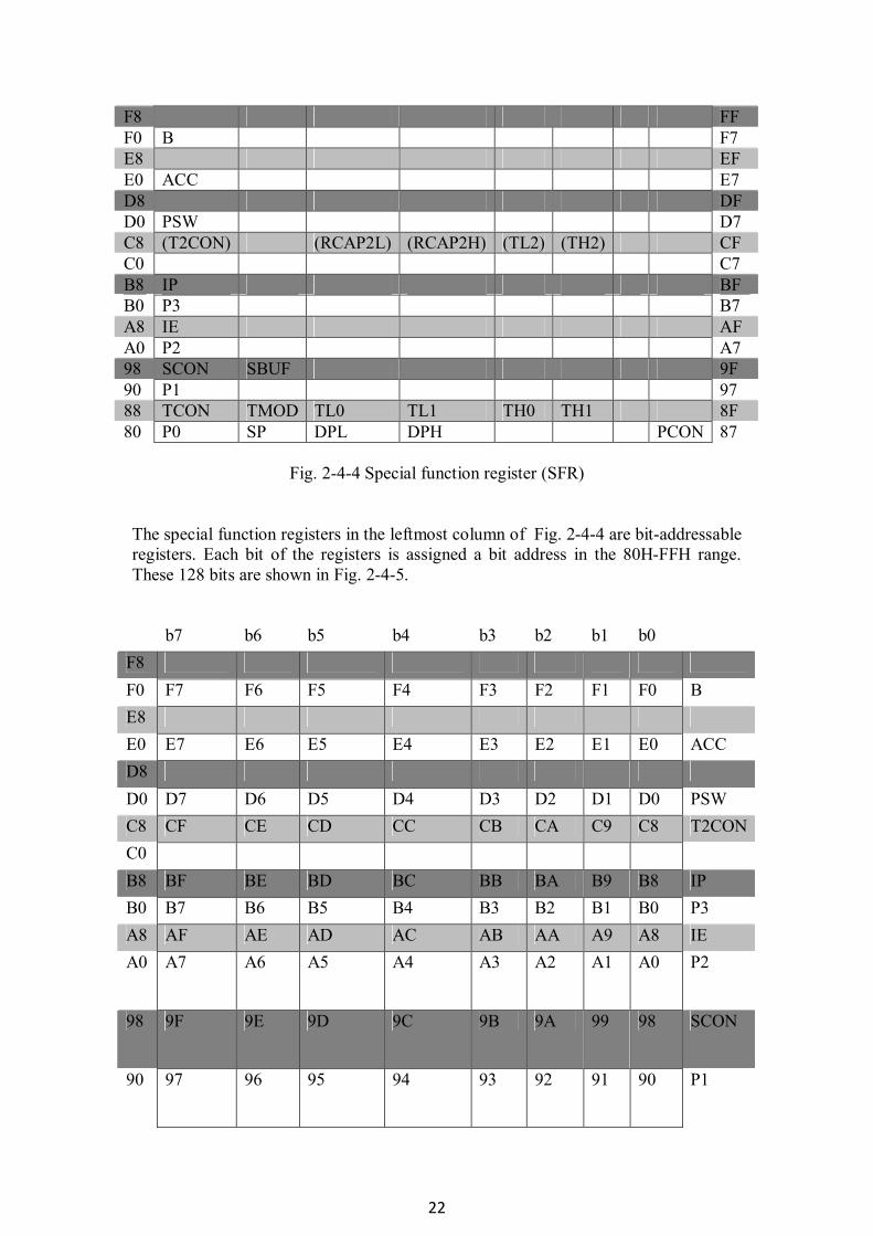
Sets the stack pointer to 3FH. The value is then saved in the memory address 40H by the following PUSH instruction. In 8052 internal data memory the locations 80H-FFH are defined by the user and must be accessed by indirect addressing. Therefore these locations are not be used as a stack Special Function Registers (SFRs) Special function registers (SFRs) include the I/O port latches, timers, peripheral controls, etc These registers can only be accessed by direct addressing A map of the SFR memory is shown in Fig. 2-4-4. The register bracketed are for 8052 only.
22
F8 FF F0 B F7 E8 EF E0 ACC E7 D8 DF D0 PSW D7 C8 (T2CON) (RCAP2L) (RCAP2H) (TL2) (TH2) CF C0 C7 B8 IP BF B0 P3 B7 A8 IE AF A0 P2 A7 98 SCON SBUF 9F 90 P1 97 88 TCON TMOD TL0 TL1 TH0 TH1 8F 80 P0 SP DPL DPH PCON 87
Fig. 2-4-4 Special function register (SFR) The special function registers in the leftmost column of Fig. 2-4-4 are bit-addressable registers. Each bit of the registers is assigned a bit address in the 80H-FFH range. These 128 bits are shown in Fig. 2-4-5.
b7 b6 b5 b4 b3 b2 b1 b0 F8 F0 F7 F6 F5 F4 F3 F2 F1 F0 B E8 E0 E7 E6 E5 E4 E3 E2 E1 E0 ACC D8 D0 D7 D6 D5 D4 D3 D2 D1 D0 PSW C8 CF CE CD CC CB CA C9 C8 T2CON C0 B8 BF BE BD BC BB BA B9 B8 IP B0 B7 B6 B5 B4 B3 B2 B1 B0 P3 A8 AF AE AD AC AB AA A9 A8 IE A0 A7 A6 A5 A4 A3 A2 A1 A0 P2
98 9F 9E 9D 9C 9B 9A 99 98 SCON
90 97 96 95 94 93 92 91 90 P1
23
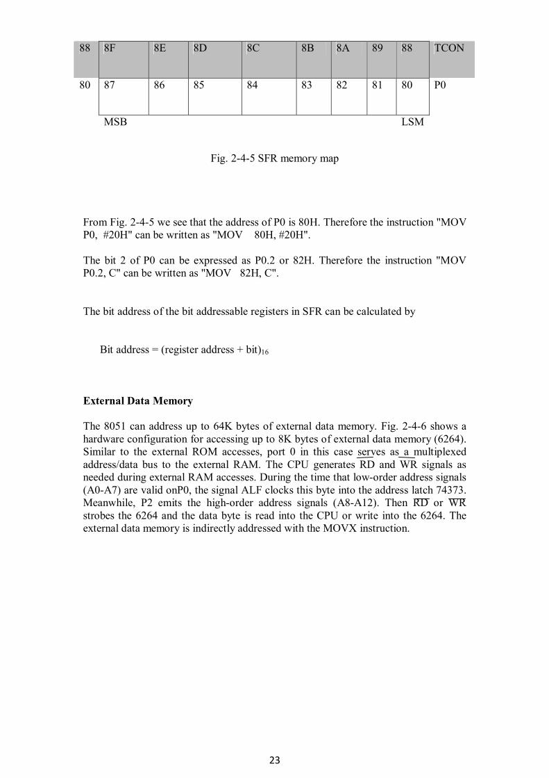
88 8F 8E 8D 8C 8B 8A 89 88 TCON
80 87 86 85 84 83 82 81 80 P0
MSB LSM
Fig. 2-4-5 SFR memory map From Fig. 2-4-5 we see that the address of P0 is 80H. Therefore the instruction "MOV P0, #20H" can be written as "MOV 80H, #20H". The bit 2 of P0 can be expressed as P0.2 or 82H. Therefore the instruction "MOV P0.2, C" can be written as "MOV 82H, C". The bit address of the bit addressable registers in SFR can be calculated by Bit address = (register address + bit)16
External Data Memory The 8051 can address up to 64K bytes of external data memory. Fig. 2-4-6 shows a hardware configuration for accessing up to 8K bytes of external data memory (6264). Similar to the external ROM accesses, port 0 in this case serves as a multiplexed address/data bus to the external RAM. The CPU generates RD and WR signals as needed during external RAM accesses. During the time that low-order address signals (A0-A7) are valid onP0, the signal ALF clocks this byte into the address latch 74373. Meanwhile, P2 emits the high-order address signals (A8-A12). Then RD or WR strobes the 6264 and the data byte is read into the CPU or write into the 6264. The external data memory is indirectly addressed with the MOVX instruction.
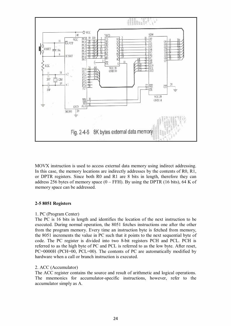
24
MOVX instruction is used to access external data memory using indirect addressing. In this case, the memory locations are indirectly addresses by the contents of R0, R1, or DPTR registers. Since both R0 and R1 are 8 bits in length, therefore they can address 256 bytes of memory space (0 – FFH). By using the DPTR (16 bits), 64 K of memory space can be addressed. 2-5 8051 Registers 1. PC (Program Center) The PC is 16 bits in length and identifies the location of the next instruction to be executed. During normal operation, the 8051 fetches instructions one after the other from the program memory. Every time an instruction byte is fetched from memory, the 8051 increments the value in PC such that it points to the next sequential byte of code. The PC register is divided into two 8-bit registers PCH and PCL. PCH is referred to as the high byte of PC and PCL is referred to as the low byte. After reset, PC=0000H (PCH=00, PCL=00). The contents of PC are automatically modified by hardware when a call or branch instruction is executed. 2. ACC (Accumulator) The ACC register contains the source and result of arithmetic and logical operations. The mnemonics for accumulator-specific instructions, however, refer to the accumulator simply as A.
25
3. PSW (Program Status Word) The PSW register contains program status information as detailed in Fig. 2-5-1. The PSW register is bit addressable. Therefore PSW.7 in an instruction stands of CY flag (C), and PWS.4 stands of RS1
CY AC F0 RS1 RS0 OV P MSB LSB Fig. 2-5-1 PSW bit diagram
CY: Carry flag. The CY is set if there is a carry-out or borrow-in for the MSB of the result during the execution of an arithmetic instruction. Otherwise, CY is reset. AC: Auxiliary Carry flag. The AC is set if there is a carry-out from the low nibble into the high nibble or a borrow-in from the high nibble into the low nibble. Otherwise, AC is reset. This flag can be used in the adjustment of binary to BCD. F0: Flag 0 is available to the user for general purposes. RS0, RS1: Register bank select bits 0 and 1. OV: Overflow flag. When OV is set, It indicates that the signed result is out of range. If the result is not out of range, OV remains reset. P: Parity bit. The P flag is set if the result produce by the instruction has odd parity, that is, if it contains an odd number of bits at the 1 logic level. If parity is even, P flag is reset.
4. B(B register) The B register is used during multiply and divide executions. For other instructions it can be treated as another scratch-pad register. 5. IP (Interrupt priority register) The IP register is use to define the priority levels (high and low) of interrupt resources. 6. IE(Interrupt enable register) The IE register is used to enable or disable the interrupt resources. 7. SBUF (Serial data buffer) The SBUF is actually two separate registers: one transmit buffer register and one receive buffer register. When a data byte is moved to SBUF, it goes to the transmit buffer where it is held for serial transmission. When a data byte is moved from SBUF, it comes from the receiver buffer. 8. SCON(Serial control register) The serial control register ad status register contains not only the mode selection bits, but also the 9th data bit for transmit and receive (TB8 and RB8), and the serial port interrupt bits (T1 and R1). 9. TH1, TL1(Timer/counter 1 register high low bytes)
26
The two 8-bit registers are used to store the count value of timer counter 1. 10. TH0, TL0(Timer/counter 0 register ) The two 8-bit registers are used to store the count value of timer/counter 0. 11. TMOD(Timer/counter mode control register) It is used to define the operating modes of timer/ counters. Timer or counter selection. 12. TCON(Timer /counter control register) It contains the overflow flags and run control bits of timer counters, and the edge flag and type control bits of interrupts. 13. DPH, DPL(data pointer high and low bytes ) 8051 has two 16-bit registers: one is the program counter (PC) and the other is data pointer register (DPTR). The data pointer consists of a high byte (DPH) and a low byte (DPL). Its intended function is to hold a 16-bit address. It may be manipulated as a 16-bit register or as two independent 8-bit registers. 14. PCON(Power control Register) It contains the double baud rate bit (SMOD), idle mode (IDL) bit and power down mode (PD) bit. 15. SP(Stack pointer) It is 8-bit wide. It is incremented before data is stored during PUSH and CALL executions. While the stack may reside anywhere in on-chip RAM, the stack pointer is initialized to 07H after a reset. This causes the stack to begin at location 08H. 16. P0,P1, P2, and P3( I/O portsn0 to 3) The P0, P1, P2, and P3 are the SFR latches of 8051 I/O ports 0, 1, 2, and 3, respectively. 17. TH2,TL2(Timer/counter 2 high and low bytes) The two 8-bit registers are used to store the count value of the timer/ counter 2. The timer/counter 2 is resident in the 8052 only. 18. RCAP2H, RCAP2L( timer/counter 2 capture register high and low bytes) The register pair (RCAP2H, RCAP2L) is the capture register for the timer 2 capture mode. In this mode, in response to a transition at the 8052's T2EX pin, TH2 and TL2 are copied into RCAP2H and RCAP2L. timer/counter 2 also have a 16-bit auto-reload mode, and RCAP2H and RCAP2L hold the reload value for this mode. 19. T2CON (Timer/counter 2 control register). The contents of SFR after reset are shown in Table 2-5-1)
27
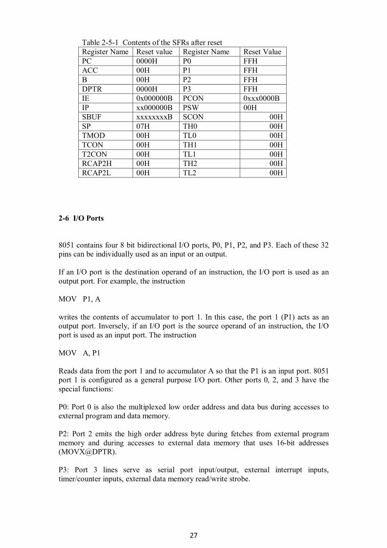
Table 2-5-1 Contents of the SFRs after reset Register Name Reset value Register Name Reset Value PC 0000H P0 FFH ACC 00H P1 FFH B 00H P2 FFH DPTR 0000H P3 FFH IE 0x000000B PCON 0xxx0000B IP xx000000B PSW 00H SBUF xxxxxxxxB SCON 00H SP 07H TH0 00H TMOD 00H TL0 00H TCON 00H TH1 00H T2CON 00H TL1 00H RCAP2H 00H TH2 00H RCAP2L 00H TL2 00H
2-6 I/O Ports 8051 contains four 8 bit bidirectional I/O ports, P0, P1, P2, and P3. Each of these 32 pins can be individually used as an input or an output. If an I/O port is the destination operand of an instruction, the I/O port is used as an output port. For example, the instruction MOV P1, A writes the contents of accumulator to port 1. In this case, the port 1 (P1) acts as an output port. Inversely, if an I/O port is the source operand of an instruction, the I/O port is used as an input port. The instruction MOV A, P1
Reads data from the port 1 and to accumulator A so that the P1 is an input port. 8051 port 1 is configured as a general purpose I/O port. Other ports 0, 2, and 3 have the special functions: P0: Port 0 is also the multiplexed low order address and data bus during accesses to external program and data memory. P2: Port 2 emits the high order address byte during fetches from external program memory and during accesses to external data memory that uses 16-bit addresses (MOVX@DPTR). P3: Port 3 lines serve as serial port input/output, external interrupt inputs, timer/counter inputs, external data memory read/write strobe.
28
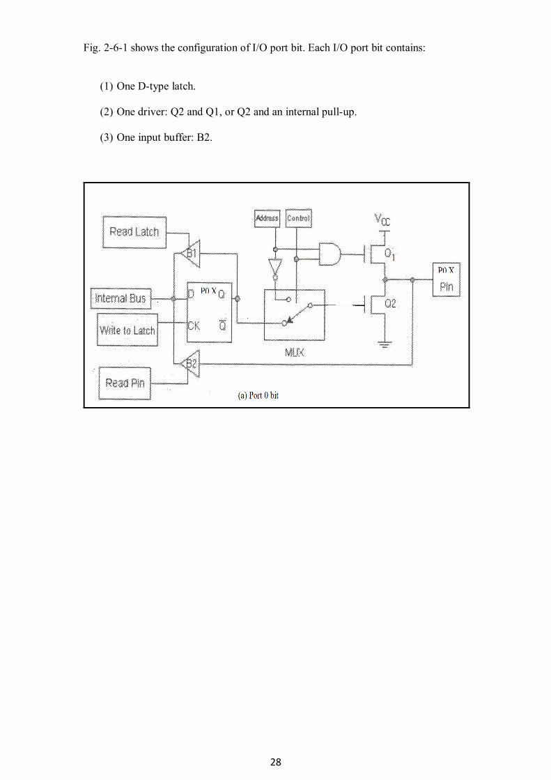
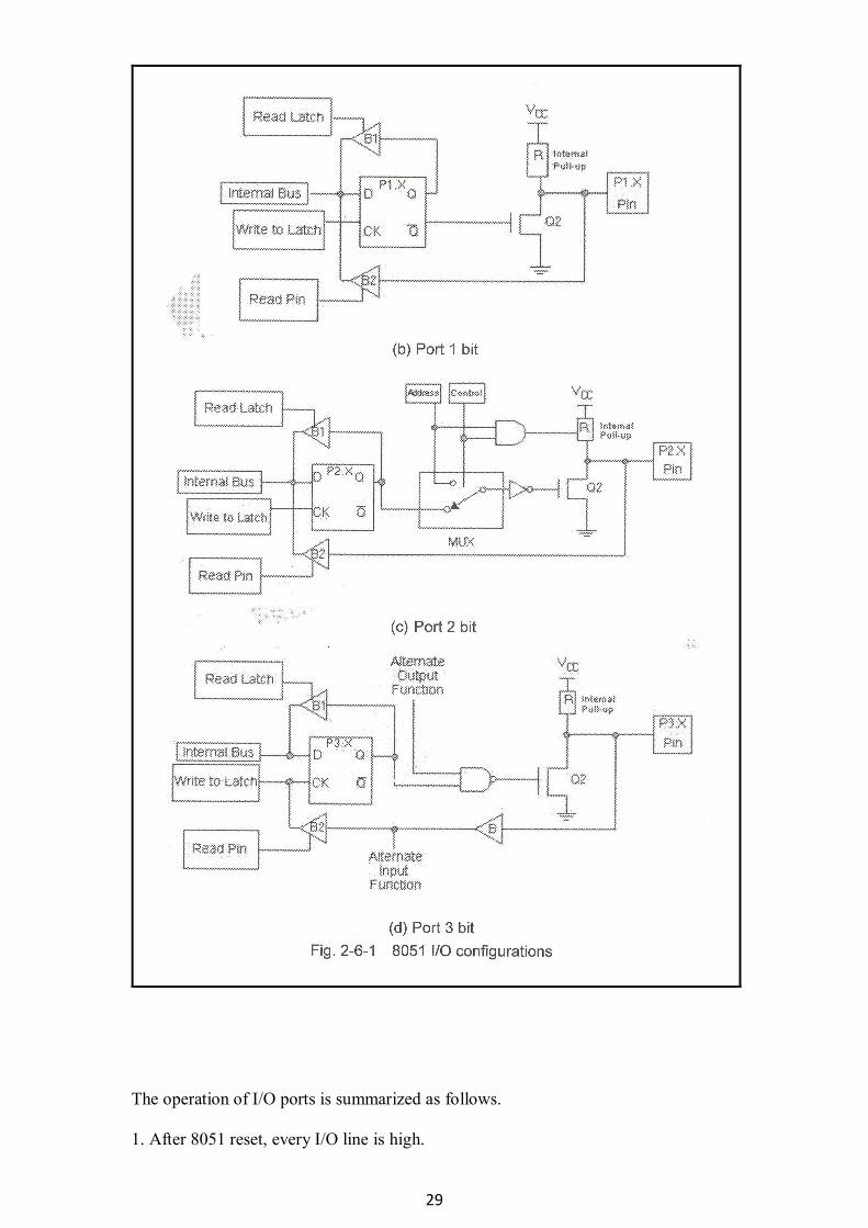
Fig. 2-6-1 shows the configuration of I/O port bit. Each I/O port bit contains:
(1) One D-type latch.
(2) One driver: Q2 and Q1, or Q2 and an internal pull-up.
(3) One input buffer: B2.
29
The operation of I/O ports is summarized as follows. 1. After 8051 reset, every I/O line is high.
30
2. When used as an output, the output data is latched in the d flip-flop until the next data is written. The output of flip-flop is directed to internal bus through the buffer B1 activated by the ''read latch'' signal. 3. When used as an input, the data on I/O pin is directly presented on the internal bus through the B2 buffer activated by the read pin control. 4. To input data pin to an I/O port pin, a 1 must be first written to port bit to turn off the Q2. 5. P0 has no internal pull-ups. When used as an output port, external pull-ups (generally 2.2K) are needed to provide high voltage potential. 6. During read operation, the read data on internal data bus can be: 1 data I the latch if the read latch signal is active or 2 data on the pin if the read pin signal is active. Some instructions that read a port read the latch rather than the pin are the ones that read a value, possibly change it, and then rewrite it to the latch. These instructions are called read-modify-write instructions as listed in Table 2-6-1. When the destination operand is a port, or a port bit, these instructions read the latch rather than the pin. Table 2-6-1 Read-Modify-Write Instructions Instruction Operation Example
ANL Logical AND ANL P1,A
ORL Logical OR ORL P1,A
XRL Logical XOR XRL P1,A
JBC Jump if the test bit is set JBC P1.1, NEXT
INC Increment INC P1
DEC Decrement DEC P1
CPL Complement CPL P1.1
DJNZ Jump if non-zero after decrement
DJNZ P1, NEXT
MOV Px.x, C Mov carry flag to Px.x bit MOV 1.1, C
CLR Px.x Clear Px.x bit CLR P1.1
SETB Px.x Set Px.x bit SETB P1.1
7. P0 and P2 serve multiplexed address/data function. The multiplexer is used for address bit and data bit selection. 8. Port 1 is configured as a general purpose I/O.
31
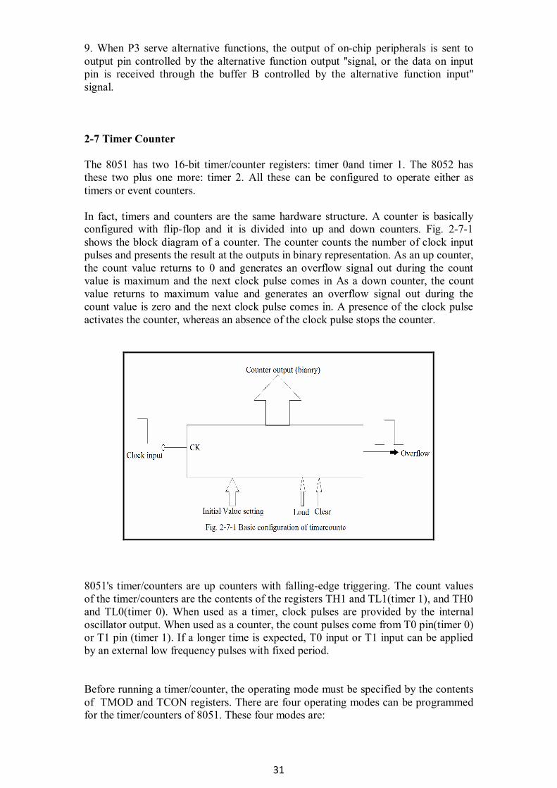
9. When P3 serve alternative functions, the output of on-chip peripherals is sent to output pin controlled by the alternative function output ''signal, or the data on input pin is received through the buffer B controlled by the alternative function input'' signal. 2-7 Timer Counter The 8051 has two 16-bit timer/counter registers: timer 0and timer 1. The 8052 has these two plus one more: timer 2. All these can be configured to operate either as timers or event counters. In fact, timers and counters are the same hardware structure. A counter is basically configured with flip-flop and it is divided into up and down counters. Fig. 2-7-1 shows the block diagram of a counter. The counter counts the number of clock input pulses and presents the result at the outputs in binary representation. As an up counter, the count value returns to 0 and generates an overflow signal out during the count value is maximum and the next clock pulse comes in As a down counter, the count value returns to maximum value and generates an overflow signal out during the count value is zero and the next clock pulse comes in. A presence of the clock pulse activates the counter, whereas an absence of the clock pulse stops the counter.
8051's timer/counters are up counters with falling-edge triggering. The count values of the timer/counters are the contents of the registers TH1 and TL1(timer 1), and TH0 and TL0(timer 0). When used as a timer, clock pulses are provided by the internal oscillator output. When used as a counter, the count pulses come from T0 pin(timer 0) or T1 pin (timer 1). If a longer time is expected, T0 input or T1 input can be applied by an external low frequency pulses with fixed period. Before running a timer/counter, the operating mode must be specified by the contents of TMOD and TCON registers. There are four operating modes can be programmed for the timer/counters of 8051. These four modes are:
32
Mode 0: 13-bit timer/counter Mode 1: 16-bit timer/counter Mode 2: 8-bit auto reload timer/counter Mode 3: Two indivitual8-bit timer/counter The 8051 has two on –chip timer/counters with the same configuration as shown in Fig. 2-7-2. The notation ''X'' stands of 1 or 0, 0 for timer 0 and 1 for timer 1.
A brief explanation of 8051 timer/counter operation is made by referring to Fig. 2-7-2. 1. The counter consists of TLX and THX where THX is high byte and TLX is low byte. During an overflow occurs, the overflow flag TFX is set to request CPU to interrupt. If the request is acknowledged by the CPU, TFX is automatically cleared. 2. There are two possible sources of clock signal. They are: (1) TX external input (2) Divide-by-12 prescaler output (1/12 the oscillator frequency). If the oscillator frequency is 12 MHz, the prescaler output frequency is thus 1 MHz, and the counter increments its contents per microsecond. These two input sources are selected with the C/T bit in the TMOD register. 3. The clock signal selected by the C/T bit is further controlled by a switch. This switch is controlled by the logic (GATE + INTX).TRX, where TRX bit locates in TMOD register, GATE bit locates in TCON register. Both TRX and GATE are set or cleared by software. INTX indicates external interrupt input; that is, IINT0 for timer 0 and INT1 for timer 1. If (GATE+INTX) .TRX=1, the switch is turned on and the counter is activated. There are three cases to activate the counter:
33
(1) If the GATE bit is cleared, a set TRX will start the counter and a cleared TRX will stop the counter. This is known as software control. In this case, the INTX input is reserved for interrupt input. (2) If both TRX and GATE are set, INTX=1 will start the counter. Otherwise, INTX=0, will stop the counter, this is known as hardware control and is suited for purpose of pulse width measurements as shown in Fig. 2-7-3.
(3) If TRX bit is set and INTX is wired to ground, a cleared GATE will start the counter and a set GATE will stop the counter. This is also called as software control. Timer/counter mode control register (TMOD) located at the address 89H of SFR is not bit addressable. Its bit diagram is shown below.
In the TMOD register, lower 4 bits are for timer 0 and higher 4 bits are for timer 1. Bits M1 and M0 are used to specify the operating modes of timer/counters. M1M0=00 Mode 0, 13-bit timer/counter M1M0=01 Mode 1, 16-bit timer/counter M1M0=10 Mode 2, 8-bit timer/counter M1M0=11 Mode 3, two individual 8-bit timer/counter The TCON, timer/counter control register, is bit addressable and is within SFR at address 88H. Its bit diagram is shown below.

34
In this register, bits 4-7 are for timer/counters and bits 0-3 are for external interrupts. TF1 (TCON.7): Timer/counter 1 overflow flag. It set by hardware on timer/counter overflow and cleared by hardware when processor vectors to interrupt routine. TR1 (TCON.6): Timer/counter 1 run control bit. It is set/ cleared by software to run timer/counter on/off. Set and cleared by the instructions SETB TR1 and CLR TR1, respectively. TF0 (TCON.5): Timer/counter 0 overflow flag. It is set by hardware on timer/counter overflow and cleared by hardware when processor vectors to interrupt routine. TR0 (TCON.4): Timer/counter 1 run control bit. It is set/ cleared by software to run timer/counter on/off. IE1 (TCON.3): External interrupt 1 edge flag. It is set by hardware when external interrupt edge detected and cleared when interrupt processed. IT1 (TCON.2): External interrupt 1 type control bit. It is set/ cleared by software to specify falling edge/low level triggering external interrupt. IE0 (TCON.1): external interrupt 1 type control bit. It is set/ cleared by software to specify falling edge/low level triggering external interrupt. 2-8 Serial Port Data transmission can be divided into two categories: parallel and serial. Parallel transmission sends or receives multiple data bits (generally 8 bits) At the same time. Parallel transmission has the advantage of high speed and the disadvantage of the interference caused by more wires. Therefore it is suitable for the applications of short-distance (less than 10 meters) transmission, such as personal computer to printer. Serial transmission transmits and receives one data bit per time interval on a wire. Serial transmission has the advantage of no interference and the disadvantage of low speed. It is suited for the applications of long-distance transmission, such as the communication between personal computer and mouse or MODEM.Fig2-8-1and 2-8-2 show the connections of parallel transmission and serial transmission, respectively. Parallel transmission is simply achieved by using 8-bit I/O ports as shown in Fig.2-8-1. Computer A transmits data bits 10110101 to computer B in parallel. In serial transmission, serial-to-parallel and parallel-to-serial converters must be used, since the internal data bus of microcontroller is parallel. As shown in Fig. 2-8-2, the parallel data 10110101 is first converted to serial format by the parallel-to-serial converter on computer A, and then is sent bit by bit to the serial-to-parallel converter On computer B .The serial-to-parallel converter on computer B converts the received serial data and converts it to parallel format to the parallel port of computer B. The transmit data on the transmission line of serial transmission presents as a bit stream.
35
Fig.2-8-1 Parallel transmission
8051 provides a serial transmission interface called the Universal Asynchronous Receiver/Transmitter (UART). This serial port is full duplex, meaning it can transmit and receive simultaneously. UART uses a start bit (0) to indicate that a data byte will be transmitted, and a stop bit (1) to indicate that a data byte is transmitted completely. For example, a data byte of 10110101 is transmitted through the serial port as shown in fig. 2-8-3.
36
8051 serial port interfacing is shown in Fig.2-8-4. Two wires are required for full duplex, one line for transmit and the other line for receive.
As shown in Fig. 2-8-4, the serial data buffer (SBUF) is two physically separate registers, a transmit buffer and a receive buffer. In 8051serial transmission, the data is transmitted through TXD when it is written to the transmit SBUF. The data received is stored in stored in the receive SBUF through RXD. For example, the instruction
MOV SBUF,A Moves the contents of accumulator to the serial data buffer and exits through TXD output, and the instruction
MOV A,SBUF Loads accumulator with the received data in serial data buffer.
37
8051 UART interrupt flags TI and RI are used to tell the CPU that a data byte is transmitted and received, respectively. TI: Transmit interrupt flag. It is set by hardware at the end of the 8th bit time in mode0, or at the beginning of the stop bit in the other modes. It must be cleared by software . RI: receive interrupt flag. It is set by hardware at the end of the 8th bit time in mod 0, or halfway through the stop bit time in the other modes. It must be cleared by software. Both RI and TI flags are cleared by software because the same interrupt vector 0023H is used for transmit and receive interrupts. In other words, if a serial port interrupt is acknowledged, the CPU will execute the interrupt service routine resident in the memory location 0023H. In a full-duplex system, transmit and receive interrupt service routines do different things therefore flags RI and TI are used to determine which routine to be executed. In contrast, only an interrupt (transmit or receive) could be occurred in a simplex system. 8051 Registers Related to Serial Port Registers SBUF and SCON are the most important registers in UART operation. 1. SBUF: Serial Data Buffer The SBUF is actually two separate registers, one transmit buffer register and one receive buffer register. When a byte data is moved to SBUF, it goes to the transmit buffer where it is held for serial transmission. When a byte data is moved from SBUF, it comes from the receive buffer. 2. SCON: Serial Port Control Register The serial port control and status register SCON locates in the address 98H of SFR. Its bit diagram is shown below. This register contains not only the mode selection bits, but also the 9th data bit for transmit and receive (TB8 and RB8), and the serial port interrupt bits (TI and RI).
SM0 SM1 SM2 REN TB8 RB8 TI RI
1. SM0 (SCON.7): Serial port mode select bit 0 2. SM1 (SCON.6): Serial port mode select bit1
There are four modes in UART operation specified by the bits SM0 and SM1. A table of these four modes is shown below.
SM0 SM1 Mode Function Baud Rate 0 0 0 Shift register Fosc/12 0 1 1 8-bit UART Software Programmable 1 0 2 9-bit UART Fosc/32 or fosc/64 1 1 3 9-bit UART Software Programmable
38
Mode 0 is usually used to expand the I/O lines. Modes 1 to 3 are for data transmission. The key differences among different operating modes are the number of data bits and baud rates. 3. SM2 (SCON.5) This bit enables the multiprocessor communication featurein modes 2 and 3.
In mode 0, SM2 should be 0. In mode 1, if SM2=1 then RI will not be activated if a valid stop bit was not received. In mode 2 or 3, if SM2=1 then RI will not be activated if the received 9th data bit (RB8) is 0. 4. REN (SCON.4): Serial reception enable bit. This bit enables serial reception. Set by software to enable reception and cleared by software to disable reception. If REN=1, The UART is enabled to receive, otherwise, the UART is disabled to receive. 5. TB8 (SCON.3):9th data bit. This bit is the 9th bit that will be transmitted in modes 2and 3. Set or cleared by software as desired. 6. RB8 (SCON.2): Stop bit or 9th data bit received In mode 0, this bit is not used . In mode 1, if SM2=0, RB8 is the stop bit that was received . In modes 2and 3, RB8 is the 9th data bit that was received. 7. TI (SCON.1): Transmit interrupt flag Set by hardware at the end of the 8th bit time in mode 0, or at the beginning of the stop bit in the other modes, in any serial transmission. This flag must be cleared by software. 8. RI (SCON.0): Receive interrupt flag Set by hardware at the end of the 8th bit time in mode 0, or halfway through the stop bit time in the other modes, in any serial reception (except see SM2). This flag must be cleared by software. In addition, the SMOD bit in the power control register (PCON) involves in the selection of UART baud rates.
Power Control Register (PCON) The PCON register locates at the address 87H in SFR. Its bit diagram is shown below.
SMOD GF1 GF0 PD IDL
SMOD: Double baud rate bit. If SMOD=1, the baud rate will be twice the baud rate as SMOD=0. GF1,GF0: General –purpose flag bits.
39
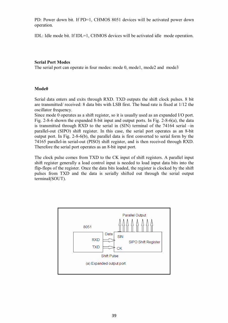
PD: Power down bit. If PD=1, CHMOS 8051 devices will be activated power down operation. IDL: Idle mode bit. If IDL=1, CHMOS devices will be activated idle mode operation. Serial Port Modes The serial port can operate in four modes: mode 0, mode1, mode2 and mode3 Mode0 Serial data enters and exits through RXD. TXD outputs the shift clock pulses. 8 bit are transmitted/ received: 8 data bits with LSB first. The baud rate is fixed at 1/12 the oscillator frequency. Since mode 0 operates as a shift register, so it is usually used as an expanded I/O port. Fig. 2-8-6 shown the expanded 8-bit input and output ports. In Fig. 2-8-6(a), the data is transmitted through RXD to the serial in (SIN) terminal of the 74164 serial –in parallel-out (SIPO) shift register. In this case, the serial port operates as an 8-bit output port. In Fig. 2-8-6(b), the parallel data is first converted to serial form by the 74165 parallel-in serial-out (PISO) shift register, and is then received through RXD. Therefore the serial port operates as an 8-bit input port. The clock pulse comes from TXD to the CK input of shift registers. A parallel input shift register generally a load control input is needed to load input data bits into the flip-flops of the register. Once the data bits loaded, the register is clocked by the shift pulses from TXD and the data is serially shifted out through the serial output terminal(SOUT).

40
The frequency of shift pulse or baud rate is equal to 1/12 the oscillator frequency. If crystal oscillator frequency is 12 MHz, one data bit will be received every 1micro second. 1. Operation
(1) In mode 0, data is transmitted or received through RXD pin and TXD pin outputs shift pulses. (2) Transmit or receive data is 8 bits in length.
(3) Baud rate= the oscillator frequency/12.
2. Control flow (1) Transmit: See Fig. 2-8-7. a. Clear SM0, SM1, and SM2 bits in the SCON register. b. Clear TI bit. c. Move data to SBUF. The data in SBUF exits from the RXD pin and the shift pulse exits from the TXD pin. d. when the 8th data bit is transmitted, the TI is set by hardware. For next data byte transmission, repeat steps b and c.
41
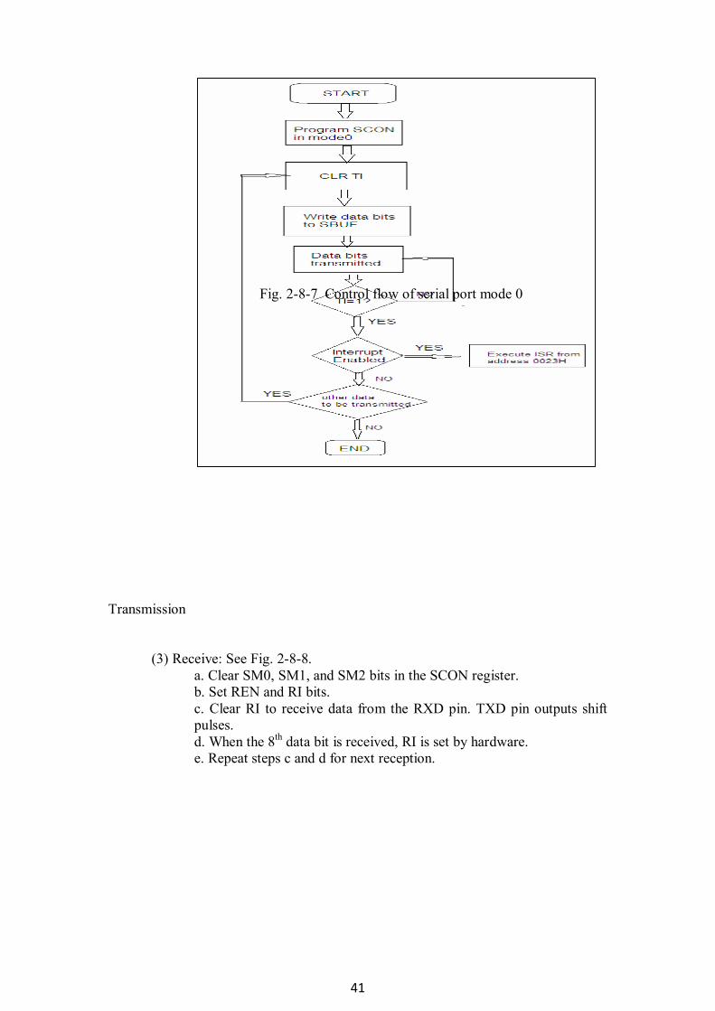
Fig. 2-8-7 Control flow of serial port mode 0 Transmission
(3) Receive: See Fig. 2-8-8. a. Clear SM0, SM1, and SM2 bits in the SCON register. b. Set REN and RI bits. c. Clear RI to receive data from the RXD pin. TXD pin outputs shift pulses. d. When the 8th data bit is received, RI is set by hardware. e. Repeat steps c and d for next reception.
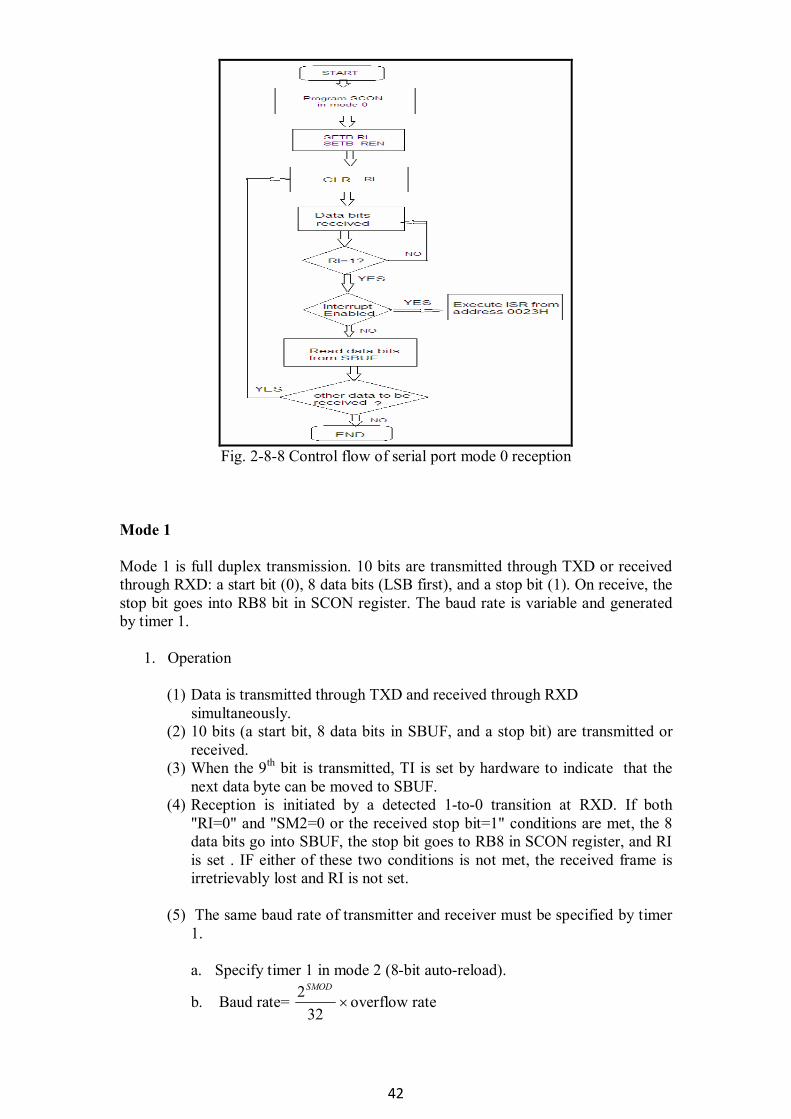
42
Fig. 2-8-8 Control flow of serial port mode 0 reception
Mode 1 Mode 1 is full duplex transmission. 10 bits are transmitted through TXD or received through RXD: a start bit (0), 8 data bits (LSB first), and a stop bit (1). On receive, the stop bit goes into RB8 bit in SCON register. The baud rate is variable and generated by timer 1.
1. Operation (1) Data is transmitted through TXD and received through RXD simultaneously. (2) 10 bits (a start bit, 8 data bits in SBUF, and a stop bit) are transmitted or
received. (3) When the 9th bit is transmitted, TI is set by hardware to indicate that the
next data byte can be moved to SBUF. (4) Reception is initiated by a detected 1-to-0 transition at RXD. If both
"RI=0" and "SM2=0 or the received stop bit=1" conditions are met, the 8 data bits go into SBUF, the stop bit goes to RB8 in SCON register, and RI is set . IF either of these two conditions is not met, the received frame is irretrievably lost and RI is not set.
(5) The same baud rate of transmitter and receiver must be specified by timer 1.
a. Specify timer 1 in mode 2 (8-bit auto-reload).
b. Baud rate= 32
2SMOD
overflow rate
43
=32
2SMOD
)1256(12 TH
frequencyoscillator
=32
2SMOD
)1256(
1THlemachinecyc
=32
2SMOD
countvalue
1
The over flow rate is defined as the number of overflows per second, that is, the reciprocal of the count value. The SMOD bit is in the PCON register. When SMOD =1, the generated baud rate is twice that of SMOD=0. After reset, SMOD is 0.
c. The baud rate is the serial transmission rate measured in bit per second (bps). Once the baud rate is determined, the initial value of TH1 can be calculated by:
TH1= 256 - baudrate
frequencyoscillatorSMOD
386
2
TH1= 256 - 32
2SMOD
baudratelemachinecyc
1
2. Control flow (1) Transmit: See Figure 2-8-9.
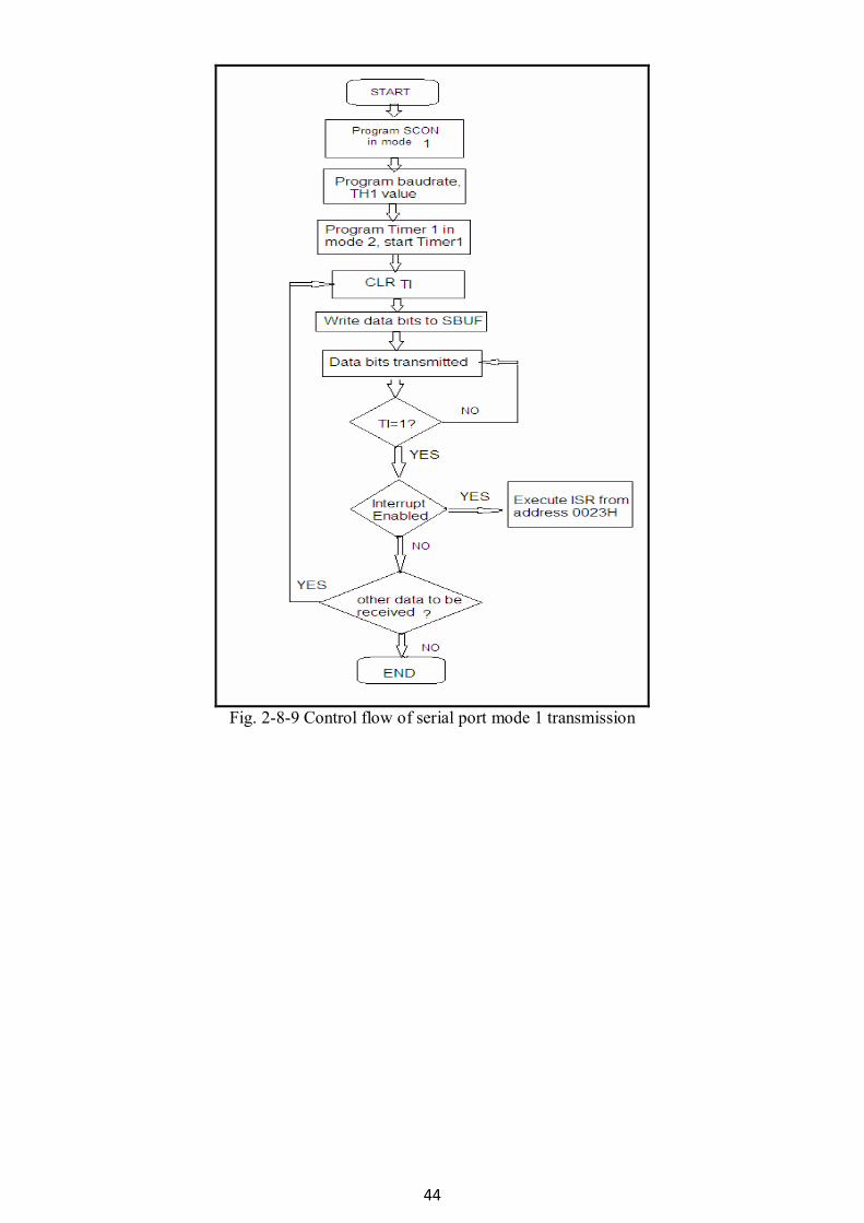
44
Fig. 2-8-9 Control flow of serial port mode 1 transmission

45
(2) Receive: See Figure 2-8-10.
Fig. 2-8-10 Control flow of serial port mode 1 reception Mode 2 In mode2, 11 bits are transmitted through TXD or received through RXD: A tart bit (0), 8 data bits (LSB first), a programmable 9th data bit, and a stop bit(1). On transmit, the 9th data bit (TB8 in SCON) can be assigned the value of 0 or 1. Or, for example, the parity bit (P in PSW) could be moved into TB8. On receive, the 9th
46
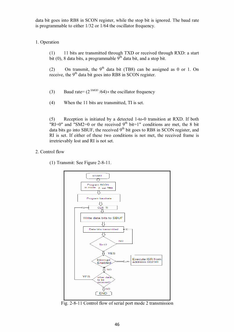
data bit goes into RB8 in SCON register, while the stop bit is ignored. The baud rate is programmable to either 1/32 or 1/64 the oscillator frequency. 1. Operation
(1) 11 bits are transmitted through TXD or received through RXD: a start bit (0), 8 data bits, a programmable 9th data bit, and a stop bit.
(2) On transmit, the 9th data bit (TB8) can be assigned as 0 or 1. On receive, the 9th data bit goes into RB8 in SCON register.
(3) Baud rate= (2 SMOD /64) the oscillator frequency
(4) When the 11 bits are transmitted, TI is set.
(5) Reception is initiated by a detected 1-to-0 transition at RXD. If both "RI=0" and "SM2=0 or the received 9th bit=1" conditions are met, the 8 bit data bits go into SBUF, the received 9th bit goes to RB8 in SCON register, and RI is set. If either of these two conditions is not met, the received frame is irretrievably lost and RI is not set.
2. Control flow
(1) Transmit: See Figure 2-8-11.
Fig. 2-8-11 Control flow of serial port mode 2 transmission
47
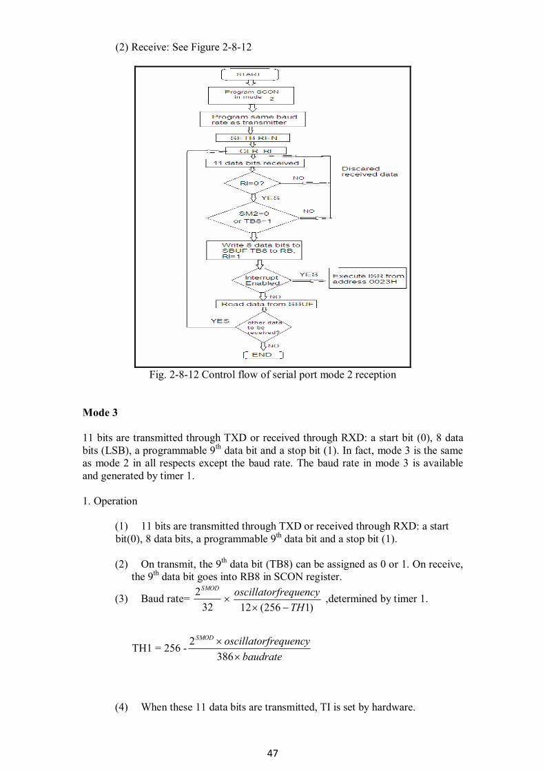
(2) Receive: See Figure 2-8-12
Fig. 2-8-12 Control flow of serial port mode 2 reception
Mode 3 11 bits are transmitted through TXD or received through RXD: a start bit (0), 8 data bits (LSB), a programmable 9th data bit and a stop bit (1). In fact, mode 3 is the same as mode 2 in all respects except the baud rate. The baud rate in mode 3 is available and generated by timer 1. 1. Operation
(1) 11 bits are transmitted through TXD or received through RXD: a start bit(0), 8 data bits, a programmable 9th data bit and a stop bit (1). (2) On transmit, the 9th data bit (TB8) can be assigned as 0 or 1. On receive,
the 9th data bit goes into RB8 in SCON register.
(3) Baud rate= 32
2SMOD
)1256(12 TH
frequencyoscillator
,determined by timer 1.
TH1 = 256 -baudrate
frequencyoscillatorSMOD
386
2
(4) When these 11 data bits are transmitted, TI is set by hardware.
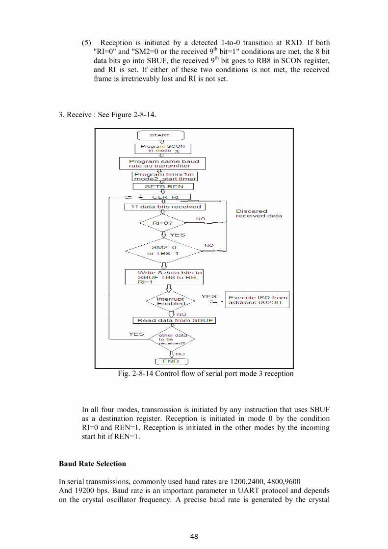
48
(5) Reception is initiated by a detected 1-to-0 transition at RXD. If both
"RI=0" and "SM2=0 or the received 9th bit=1" conditions are met, the 8 bit data bits go into SBUF, the received 9th bit goes to RB8 in SCON register, and RI is set. If either of these two conditions is not met, the received frame is irretrievably lost and RI is not set.
3. Receive : See Figure 2-8-14.
Fig. 2-8-14 Control flow of serial port mode 3 reception
In all four modes, transmission is initiated by any instruction that uses SBUF as a destination register. Reception is initiated in mode 0 by the condition RI=0 and REN=1. Reception is initiated in the other modes by the incoming start bit if REN=1.
Baud Rate Selection
In serial transmissions, commonly used baud rates are 1200,2400, 4800,9600 And 19200 bps. Baud rate is an important parameter in UART protocol and depends on the crystal oscillator frequency. A precise baud rate is generated by the crystal
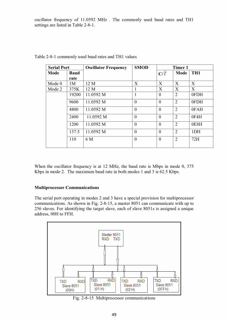
49
oscillator frequency of 11.0592 MHz . The commonly used baud rates and TH1 settings are listed in Table 2-8-1. Table 2-8-1 commonly used baud rates and TH1 values
Serial Port Timer 1 Mode Baud
rate
Oscillator Frequency SMOD C/T Mode TH1
Mode 0 1M 12 M X X X X Mode 2 375K 12 M 1 X X X
19200 11.0592 M 1 0 2 0FDH 9600 11.0592 M 0 0 2 0FDH 4800 11.0592 M 0 0 2 0FAH 2400 11.0592 M 0 0 2 0F4H 1200 11.0592 M 0 0 2 0E8H 137.5 11.0592 M 0 0 2 1DH
110 6 M 0 0 2 72H
When the oscillator frequency is at 12 MHz, the baud rate is Mbps in mode 0, 375 Kbps in mode 2. The maximum baud rate in both modes 1 and 3 is 62.5 Kbps. Multiprocessor Communications The serial port operating in modes 2 and 3 have a special provision for multiprocessor communications. As shown in Fig. 2-8-15, a master 8051 can communicate with up to 256 slaves. For identifying the target slave, each of slave 8051s is assigned a unique address, 00H to FFH.
Fig. 2-8-15 Multiprocessor communications
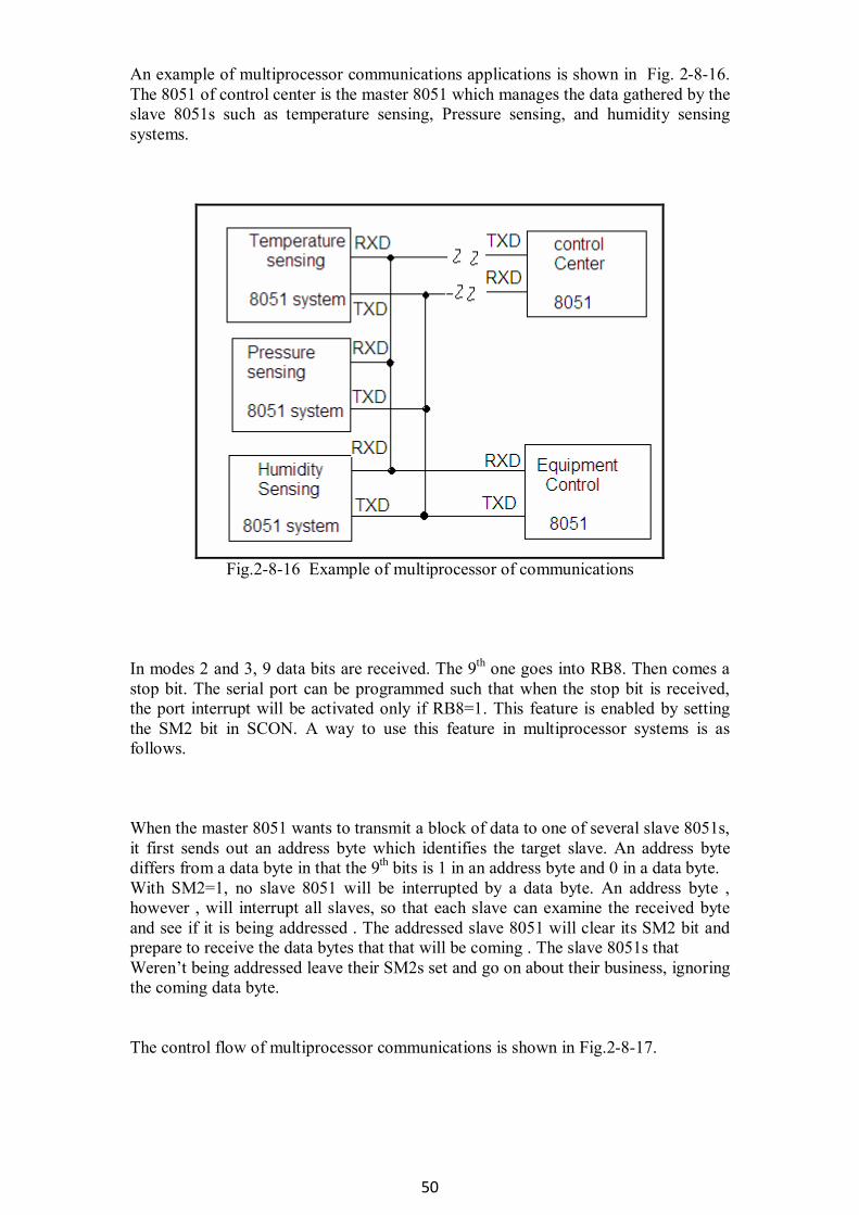
50
An example of multiprocessor communications applications is shown in Fig. 2-8-16. The 8051 of control center is the master 8051 which manages the data gathered by the slave 8051s such as temperature sensing, Pressure sensing, and humidity sensing systems.
Fig.2-8-16 Example of multiprocessor of communications
In modes 2 and 3, 9 data bits are received. The 9th one goes into RB8. Then comes a stop bit. The serial port can be programmed such that when the stop bit is received, the port interrupt will be activated only if RB8=1. This feature is enabled by setting the SM2 bit in SCON. A way to use this feature in multiprocessor systems is as follows. When the master 8051 wants to transmit a block of data to one of several slave 8051s, it first sends out an address byte which identifies the target slave. An address byte differs from a data byte in that the 9th bits is 1 in an address byte and 0 in a data byte. With SM2=1, no slave 8051 will be interrupted by a data byte. An address byte , however , will interrupt all slaves, so that each slave can examine the received byte and see if it is being addressed . The addressed slave 8051 will clear its SM2 bit and prepare to receive the data bytes that that will be coming . The slave 8051s that Weren’t being addressed leave their SM2s set and go on about their business, ignoring the coming data byte. The control flow of multiprocessor communications is shown in Fig.2-8-17.
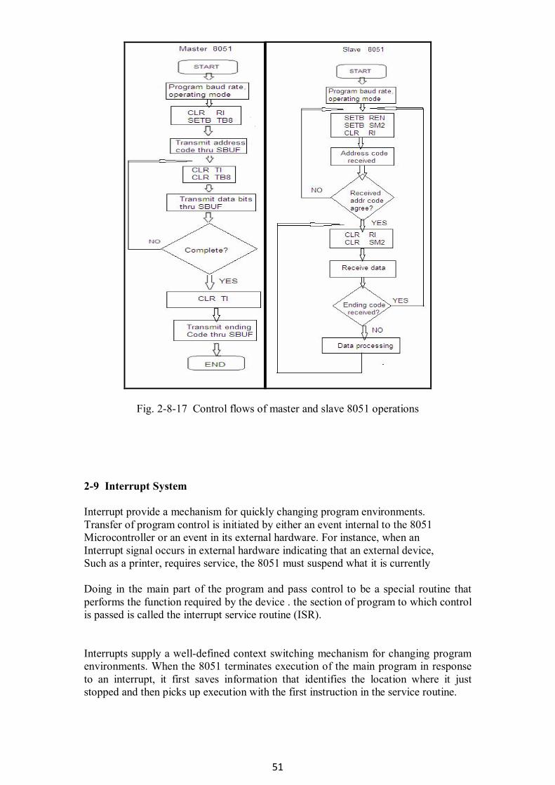
51
Fig. 2-8-17 Control flows of master and slave 8051 operations 2-9 Interrupt System Interrupt provide a mechanism for quickly changing program environments. Transfer of program control is initiated by either an event internal to the 8051 Microcontroller or an event in its external hardware. For instance, when an Interrupt signal occurs in external hardware indicating that an external device, Such as a printer, requires service, the 8051 must suspend what it is currently Doing in the main part of the program and pass control to be a special routine that performs the function required by the device . the section of program to which control is passed is called the interrupt service routine (ISR). Interrupts supply a well-defined context switching mechanism for changing program environments. When the 8051 terminates execution of the main program in response to an interrupt, it first saves information that identifies the location where it just stopped and then picks up execution with the first instruction in the service routine.
52
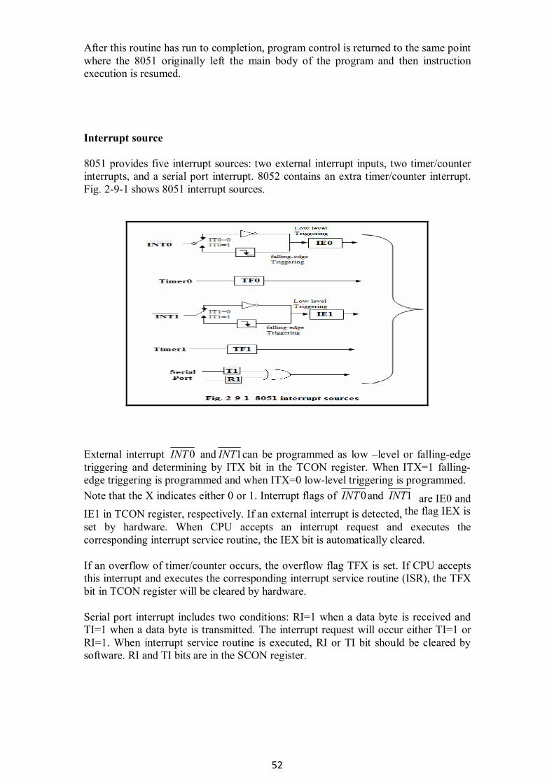
After this routine has run to completion, program control is returned to the same point where the 8051 originally left the main body of the program and then instruction execution is resumed. Interrupt source 8051 provides five interrupt sources: two external interrupt inputs, two timer/counter interrupts, and a serial port interrupt. 8052 contains an extra timer/counter interrupt. Fig. 2-9-1 shows 8051 interrupt sources.
External interrupt 0INT and 1INT can be programmed as low –level or falling-edge triggering and determining by ITX bit in the TCON register. When ITX=1 falling-edge triggering is programmed and when ITX=0 low-level triggering is programmed. Note that the X indicates either 0 or 1. Interrupt flags of 0INT and 1INT are IE0 and IE1 in TCON register, respectively. If an external interrupt is detected, the flag IEX is set by hardware. When CPU accepts an interrupt request and executes the corresponding interrupt service routine, the IEX bit is automatically cleared. If an overflow of timer/counter occurs, the overflow flag TFX is set. If CPU accepts this interrupt and executes the corresponding interrupt service routine (ISR), the TFX bit in TCON register will be cleared by hardware. Serial port interrupt includes two conditions: RI=1 when a data byte is received and TI=1 when a data byte is transmitted. The interrupt request will occur either TI=1 or RI=1. When interrupt service routine is executed, RI or TI bit should be cleared by software. RI and TI bits are in the SCON register.
53
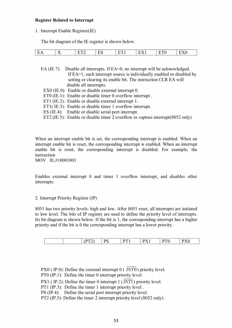
Register Related to Interrupt 1. Interrupt Enable Register(IE) The bit diagram of the IE register is shown below.
EA X ET2 ES ET1 EX1 ET0 EX0 EA (IE.7): Disable all interrupts. If EA=0, no interrupt will be acknowledged.
If EA=1, each interrupt source is individually enabled or disabled by setting or clearing its enable bit. The instruction CLR EA will disable all interrupts. EX0 (IE.0): Enable or disable external interrupt 0. ET0 (IE.1): Enable or disable timer 0 overflow interrupt . ET1 (IE.2): Enable or disable external interrupt 1. ET1( IE.3): Enable or disable timer 1 overflow interrupt. ES (IE.4): Enable or disable serial port interrupt. ET2 (IE.5): Enable or disable timer 2 overflow or capture interrupt(8052 only). When an interrupt enable bit is set, the corresponding interrupt is enabled. When an interrupt enable bit is reset, the corresponding interrupt is enabled. When an interrupt enable bit is reset, the corresponding interrupt is disabled. For example, the instruction MOV IE,#10001001 Enables external interrupt 0 and timer 1 overflow interrupt, and disables other interrupts. 2. Interrupt Priority Register (IP) 8051 has two priority levels: high and low. After 8051 reset, all interrupts are initiated to low level. The bits of IP register are used to define the priority level of interrupts. Its bit diagram is shown below. If the bit is 1, the corresponding interrupt has a higher priority and if the bit is 0 the corresponding interrupt has a lower priority.
(PT2) PS PT1 PX1 PT0 PX0
PX0 ( IP.0): Define the external interrupt 0 ( 0INT ) priority level. PT0 (IP.1): Define the timer 0 interrupt priority level. PX1 ( IP.2): Define the timer 0 interrupt 1 ( 1INT ) priority level. PT1 (IP.3): Define the timer 1 interrupt priority level . PS (IP.4): Define the serial port interrupt priority level. PT2 (IP.5): Define the timer 2 interrupt priority level (8052 only).
54
For example, the instruction MOV IP, #00010010B Defines the serial port and the external interrupt 0 as high priority level and others as low priority level. CPU handless the interrupt requests following the rules: 1. Priority within level is only to resolve simultaneous requests of the same priority level. From high to low, interrupts are:
IE0: External interrupt input TF0: Timer/counter 0 interrupt IE1: External interrupt input TF1: timer /counter 1 interrupt RI+TI: serial port interrupt TF2+EXF2: Timer/counter 2 interrupt (8052 only)
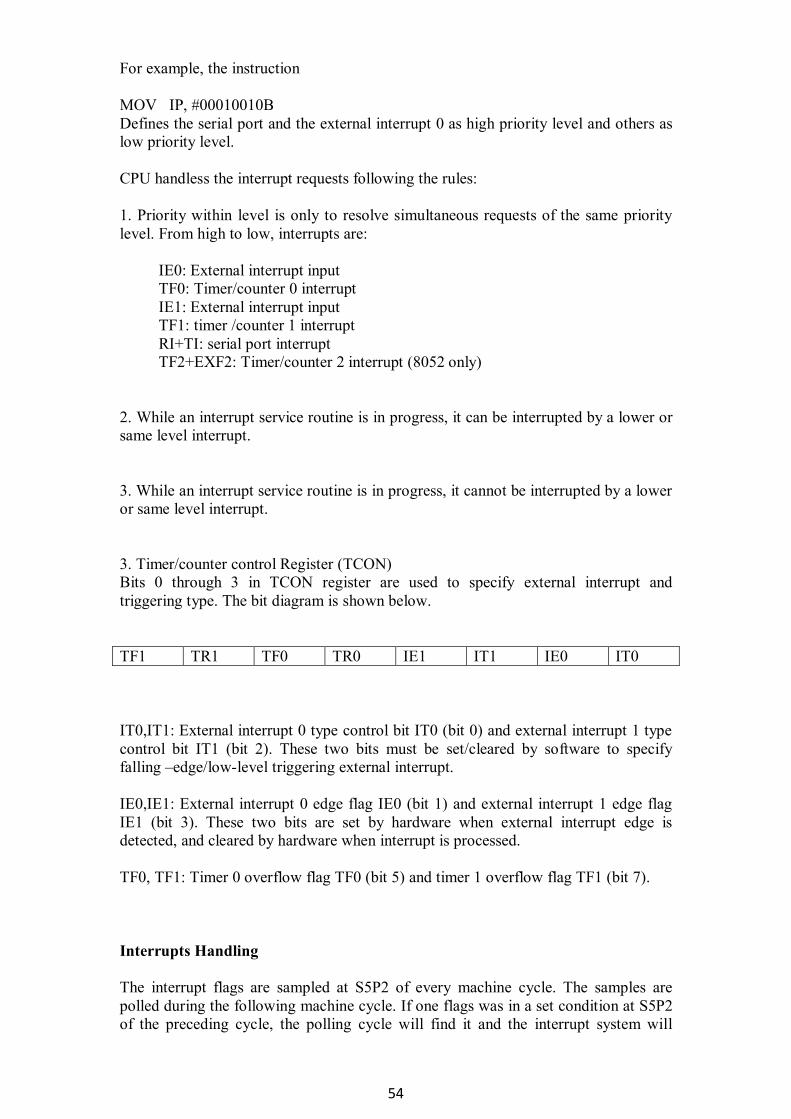
2. While an interrupt service routine is in progress, it can be interrupted by a lower or same level interrupt. 3. While an interrupt service routine is in progress, it cannot be interrupted by a lower or same level interrupt. 3. Timer/counter control Register (TCON) Bits 0 through 3 in TCON register are used to specify external interrupt and triggering type. The bit diagram is shown below. TF1 TR1 TF0 TR0 IE1 IT1 IE0 IT0 IT0,IT1: External interrupt 0 type control bit IT0 (bit 0) and external interrupt 1 type control bit IT1 (bit 2). These two bits must be set/cleared by software to specify falling –edge/low-level triggering external interrupt. IE0,IE1: External interrupt 0 edge flag IE0 (bit 1) and external interrupt 1 edge flag IE1 (bit 3). These two bits are set by hardware when external interrupt edge is detected, and cleared by hardware when interrupt is processed. TF0, TF1: Timer 0 overflow flag TF0 (bit 5) and timer 1 overflow flag TF1 (bit 7). Interrupts Handling The interrupt flags are sampled at S5P2 of every machine cycle. The samples are polled during the following machine cycle. If one flags was in a set condition at S5P2 of the preceding cycle, the polling cycle will find it and the interrupt system will
55
generate an LCALL by hardware to the appropriate vector where the first instruction of service routine is residence. The interrupt vectors of interrupt sources are: 0INT : 003H TIMER: 00BH 1INT : 013H TIMER1: 01BH UART: 023H TIMER2: 02BH (8052) only A jump instruction usually locates at interrupt vector location used to jump to a memory address where interrupt service routine starts. In the use of interrupt control, the user should attend to the following cases:
1. While an interrupt service routine is in progress, it can be interrupted by a higher
level interrupt. While an interrupt service routine is in progress, it cannot be
interrupted by a lower or same level interrupt.
2. Interrupt request signal must be held long enough to respond by the CPU.
3. While the RETI or IE and IP specified instructions are in execution, the CPU
makes no response to interrupts.
Interrupt System Control 1. Main Program (1) The starting address of main program must leave from the interrupt vector area. (2) Specify IP to determine the priority levels of interrupt sources. If only an interrupt is to be used, this step is negligible. (3) Specify IE to enable the interrupts to be used and disable unused interrupts. (4) Specify IT0 or IT1 to determine the triggering type if external interrupt are used. (5) Write main program and wait for an interrupt.

56
2. Interrupt service routine (ISR) (1) Place a jump instruction in the interrupt vector and point to the starting address of interrupt service routine. (2) Reset IE to disable other interrupts during the interrupt service routine is executing . (3) Save the contents PSW or other registers in main program onto stack using PUSH instruction. (4) Write interrupt service routine . (5) Enable interrupts. (6) Return from interrupt using RETI instruction.
Fig.2-9-2 shows the relationship among interrupt sources, interrupt flags, IE register, IP register, and interrupt priority.
2-10 Oscillator and Timing Oscillator period (Clock cycle) To generate the clock pulses required for the 8051 operation, a crystal is generally connected across X1 and X2 pins of 8051. The X1 is the input to the inverting oscillator amplifier and input to internal clock generator circuits. The X2 is the output from the inverting oscillator amplifier. The period of the Oscillator output pulse is called the oscillator period. If a 12-MHz crystal is Connected, the oscillator period is therefore equal to 1/12 microsecond. Machine cycle The machine cycles are the unit time that is needed to execute instruction. Most of 8051 instructions are 1-cycle instructions meaning that the instruction is completed in one machine cycle time.
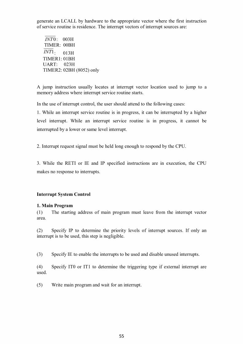
57
One machine cycle consists of 12 oscillator periods. Thus a machine cycle is s1 If a 12-MHz crystal oscillator is used. In such situation, the CPU executes a 4-cycle instruction s4 or minimum 250k instructions per second. State Each machine cycle is divided into six state : S1, S2, S3, S4, S5 and S6. Therefore one state equals to two oscillator periods. The 8051 fetches the machine code in program memory at S1 and S4 of every machine cycle. Since the first machine data byte is opcode, the opcode read at S1 is decoded by the instruction decoder. For a 1-byte instruction, the CPU discards the read data byte at S4. For a 2-byte instruction, the second data byte is read and executed in a machine cycle. Two machine cycles are required for a 3-byte instruction. Phase As mentioned above, one state consists of 2 oscillator periods. These two periods are also called as phase 1 (P1) and phase 2 (P2). The 8051 processes the instruction of arithmetic and logical operations at P1 and the data transfer between registers at P2. Also, the 8051 reads interrupt flag at S5P2. ALE and PSEN
Both ALE and PSEN signals emit twice every machine cycle during the opcode in external program memory is fetched. Fig. 2-10-1 shows the relationship among clock,
ALE, and PSEN signals. ALE and PSEN signals rise to high at S1P2 and S4P2.
The ALE signal falls to low at S2P1 and S5P1, whereas the PSEN signal falls to low at S2P2 and S5P2.
58
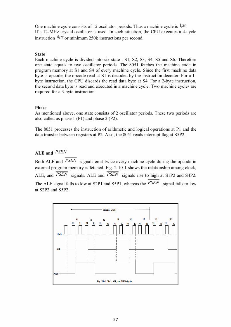
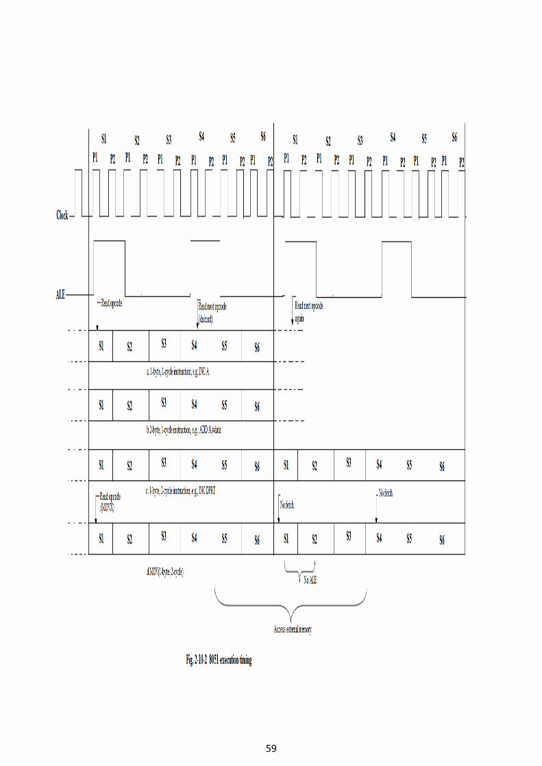
From fig.2-10-1, we see that the ALE signal has the frequency of 2MHz (at 12-MHz clock) and the duty cycle of 33.3%. The 8051 emits ALE pulses in normal operation. The PSEN signal has the frequency of 2 MHz and the duty cycle of 50%. The PSEN signal is emitted during the opcode is fetched from the external program memory. Fig.2-10-2 shows the timing diagrams for the executions of 1-byte 1-cycle, 2-byte 1-cycle, 1-byte 2-cycle, and MOVX instruction. Fig.2-10-3 shows the timing of external program memory read. The CPU fetches opcode twice every machine cycle. The address signals on ports 1 and 2 should be
ready before a 1-to-0 transition occurs on ALE signals. The PSEN signal is used to
strobe the program memory. When a 0-to-1 transition occurs on the PSEN signal, the opcode on data bus is read. In the execution of MOVX instruction, the
PSEN signal is disabled during the RD signal is activated as shown in fig.2-10-3(b).
59
60
61
2-11 ISP 8051 The newest generation of 8051 devices such as Philips P89C51RX+ family devices P89C51RC+, P89C51RD+, P89C51RX2 family devices P89C51RB2, P89C51RC2, P89C51RD2, and ATmel T89C51RC2 and T89C51RD2, equipped with on-chip flash memory and built-in loader, is widely used in the control applications since these devices are capable of in-system Programming (SP). With the ISP driver, the user can easily download the object code from PC to the 8051 device on circuit board through serial ports. The system structure is shown in fig.2-11-1.
Fig.2-11-1 ISP structure
The features of Philips P89C51RX+ family and P89C51RX2 family devices include: 1. 8051 core
2. With ISP and IAP (In-Application Programming) capabilities.
3. Speed up to 33 MHz. The clock frequency of P89C52RX can be up to 33 MHz and
every machine cycle consists of 12 oscillatoe periods. P89C51RX2 can operate at the
clock frequency of 20MHz and every machine cycle consists of 6 oscillator periods,
therefore the execution speed is doubled.
4. 4-level priority interrupt
5. 7 interrupt sources
6. Four 8-bit I/O ports and three 16-bit timer/counters.
7. With PCA (Programmable counter Array) watchdog timer.
8. Full-duplex enhanced UART with framing error detection and automatic address
recognition functions.
9. Power control modes: idle mode, Power down mode and clock can be stopped and
resumed mode.
Specifications of P89C51Rx+ and P89C51RX2 family devices are shown in tables 2-11-1 and 2-11-2, respectively.
62
Table 2-11-1 Specifications of P89C51RX+ family devices Device Flash RAM Package Temperature
Range Volt-age
Frequency (MHz)
P89C51RC+IN P89C51RC+JN
32KB 512 B 5V 0-33
P89C51RC+IA P89C51RC+JA
32KB 512B 5V 0-33
P89C51RC+IB P89C51RC+JB
32Kb 512B 5V 0-33
P89C51RD+IN P89C51RD+JN
64KB 1KB 5V 0-33
P89C51RD+IA P89C51RD+JA
64KB 1KB 5V 0-33
P89C51RD+IB P89C51RD+JB
64KB 1KB
N: 40PIN PDIP A: 44PIN 44PIN PQFP
I:0-70 C J: -40-85 C
5V 0-33
Table 2-11-2 Specifications of P89C51RX2 family devices
Frequency (MHz)
Device Flash RAM Temperature & Package
Volta-ge Range 6
Cycles 12 Cycles
P89C51RB2HBA
16KB 512B 0-70, PLCC 4.5-5.5 0-20 0-33
P89C51RB2HBBD
16KB 512B 0-70, LQFP 4.5-5.5 0-20 0-33
P89C51RC2HBP
32KB 512B 0-70, PDIP 4.5-5.5 0-2 0-33
P89C51RC2HBA
32Kb 512B 0-70, PLCC 4.5-5.5 0-20 0-33
P89C51RC2HFA
32KB 512B -40-85, PLCC 4.75-5.25
0-20 0-33
P89C51RC2HBBD
32KB 512B 0-70, LQFP 4.5-5.5 0-20 0-33
P89C51RC2HFBD
32KB 1KB -40-85,LQFP 4.75-5.25
0-20 0-33
P89C51RD2HBP
64KB 1KB 0-70,PDIP 4.5-5.5 0-20 0-33
P89C51RD2HBA
64KB 1KB 0-70, PLCC 4.5-5.5 0-20 0-33