Embed Size (px)
Citation preview
XXXX
Microarchitecture and Circuits for a 200 MHz Out-of-Order SoftProcessor Memory System
Henry Wong, University of TorontoVaughn Betz, University of TorontoJonathan Rose, University of Toronto
Although FPGAs have grown in capacity, FPGA-based soft processors have grown very little because of thedifficulty of achieving higher performance in exchange for area. Superscalar out-of-order processors promiselarge performance gains, and the memory subsystem is a key part of such a processor that must help supplyincreased performance. In this paper we describe and explore microarchitectural and circuit-level trade-offsin the design of such a memory system. We show the significant instructions-per-cycle wins for providingvarious levels of out-of-order memory access and memory dependence speculation (1.32× SPECint2000), andfor the addition of a second-level cache (another 1.60×). With careful microarchitecture and circuit design,we also achieve a L1 TLB and cache lookup with 29% less logic delay than the simpler Nios II/f memorysystem.
CCS Concepts: •Computer systems organization→ Superscalar architectures; •Hardware→ Re-configurable logic applications; Sequential circuits;
ACM Reference Format:Henry Wong, Vaughn Betz, and Jonathan Rose, 2016. Microarchitecture and Circuits for a 200 MHz Out-of-Order Soft Processor Memory System. ACM Trans. Reconfig. Technol. Syst. V, N, Article XXXX (July 2016),22 pages.DOI: http://dx.doi.org/10.1145/2974022
1. INTRODUCTIONThe ability to trade area for performance in a soft processor, beyond current soft proces-sor performance levels, would allow designers to implement more functionality in theeasier-to-use software environment. The ever-increasing logic capacity of FPGAs hasmade area much cheaper, but there has been no way to exchange this for increased soft-ware performance as soft processors have largely remained simple in-order designs.
As current commercial soft processors already achieve (for FPGAs) high clock fre-quencies, future performance gains must come from instructions-per-cycle (IPC) in-creases. There is compelling data from the evolution of hard processor microarchitec-tures that support the idea that there are significant performance gains to be had whenmoving from in-order to out-of-order processors, which we show in Table I. Each rowin Table I is a specific microarchitecture/vendor, and illustrates the net performancebenefit of the transition from in-order to out-of-order. As these processors are builtin different process technologies and the processors run at different frequencies, theperformance increases due to frequency increases are factored out. Hence, the tableshows the IPC improvement due to the transition, and this is significant in every case— ranging from 1.6 to 2 times on SPECint (95 or 2006).
Many believe that processor performance improvements derived from out-of-orderarchitectures only occur when the latency to memory is well above 100 or more pro-
Permission to make digital or hard copies of all or part of this work for personal or classroom use is grantedwithout fee provided that copies are not made or distributed for profit or commercial advantage and thatcopies bear this notice and the full citation on the first page. Copyrights for components of this work ownedby others than the author(s) must be honored. Abstracting with credit is permitted. To copy otherwise, orrepublish, to post on servers or to redistribute to lists, requires prior specific permission and/or a fee. Requestpermissions from [email protected].© 2016 Copyright held by the owner/author(s). Publication rights licensed to ACM. 1936-7406/2016/07-ARTXXXX $15.00DOI: http://dx.doi.org/10.1145/2974022
ACM Transactions on Reconfigurable Technology and Systems, Vol. V, No. N, Article XXXX, Publication date: July 2016.
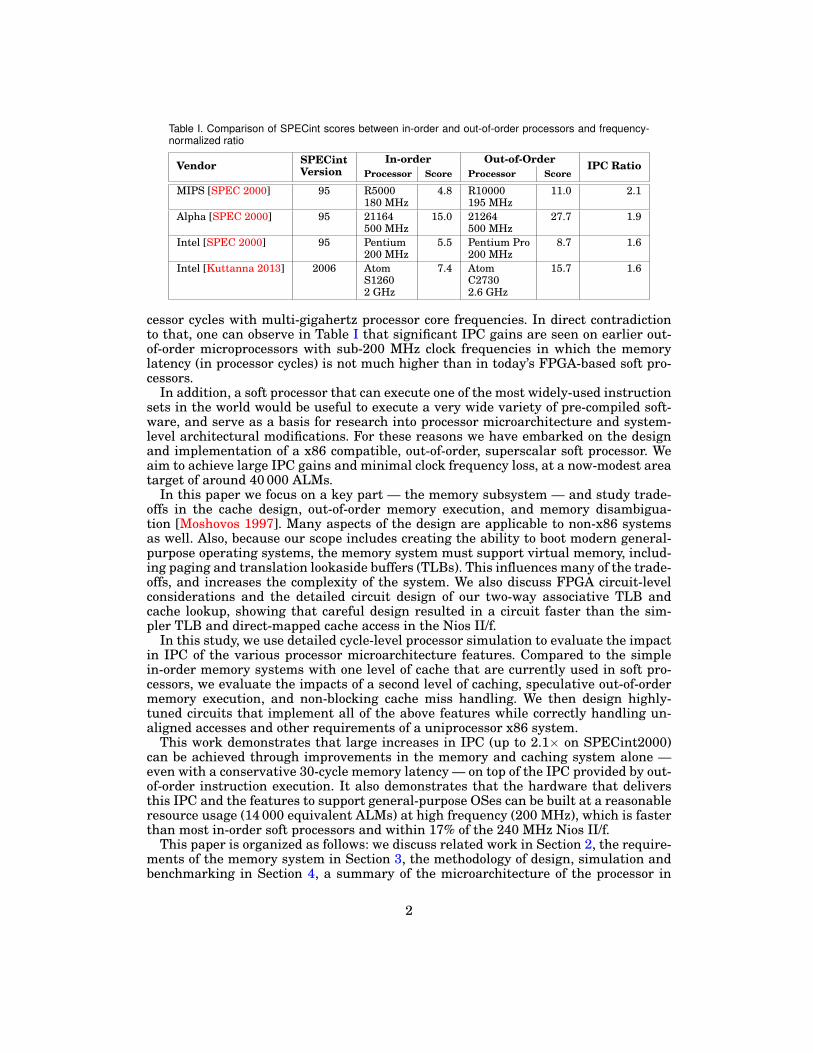
Table I. Comparison of SPECint scores between in-order and out-of-order processors and frequency-normalized ratio
Vendor SPECintVersion
In-order Out-of-Order IPC RatioProcessor Score Processor Score
MIPS [SPEC 2000] 95 R5000180 MHz
4.8 R10000195 MHz
11.0 2.1
Alpha [SPEC 2000] 95 21164500 MHz
15.0 21264500 MHz
27.7 1.9
Intel [SPEC 2000] 95 Pentium200 MHz
5.5 Pentium Pro200 MHz
8.7 1.6
Intel [Kuttanna 2013] 2006 AtomS12602 GHz
7.4 AtomC27302.6 GHz
15.7 1.6
cessor cycles with multi-gigahertz processor core frequencies. In direct contradictionto that, one can observe in Table I that significant IPC gains are seen on earlier out-of-order microprocessors with sub-200 MHz clock frequencies in which the memorylatency (in processor cycles) is not much higher than in today’s FPGA-based soft pro-cessors.
In addition, a soft processor that can execute one of the most widely-used instructionsets in the world would be useful to execute a very wide variety of pre-compiled soft-ware, and serve as a basis for research into processor microarchitecture and system-level architectural modifications. For these reasons we have embarked on the designand implementation of a x86 compatible, out-of-order, superscalar soft processor. Weaim to achieve large IPC gains and minimal clock frequency loss, at a now-modest areatarget of around 40 000 ALMs.
In this paper we focus on a key part — the memory subsystem — and study trade-offs in the cache design, out-of-order memory execution, and memory disambigua-tion [Moshovos 1997]. Many aspects of the design are applicable to non-x86 systemsas well. Also, because our scope includes creating the ability to boot modern general-purpose operating systems, the memory system must support virtual memory, includ-ing paging and translation lookaside buffers (TLBs). This influences many of the trade-offs, and increases the complexity of the system. We also discuss FPGA circuit-levelconsiderations and the detailed circuit design of our two-way associative TLB andcache lookup, showing that careful design resulted in a circuit faster than the sim-pler TLB and direct-mapped cache access in the Nios II/f.
In this study, we use detailed cycle-level processor simulation to evaluate the impactin IPC of the various processor microarchitecture features. Compared to the simplein-order memory systems with one level of cache that are currently used in soft pro-cessors, we evaluate the impacts of a second level of caching, speculative out-of-ordermemory execution, and non-blocking cache miss handling. We then design highly-tuned circuits that implement all of the above features while correctly handling un-aligned accesses and other requirements of a uniprocessor x86 system.
This work demonstrates that large increases in IPC (up to 2.1× on SPECint2000)can be achieved through improvements in the memory and caching system alone —even with a conservative 30-cycle memory latency — on top of the IPC provided by out-of-order instruction execution. It also demonstrates that the hardware that deliversthis IPC and the features to support general-purpose OSes can be built at a reasonableresource usage (14 000 equivalent ALMs) at high frequency (200 MHz), which is fasterthan most in-order soft processors and within 17% of the 240 MHz Nios II/f.
This paper is organized as follows: we discuss related work in Section 2, the require-ments of the memory system in Section 3, the methodology of design, simulation andbenchmarking in Section 4, a summary of the microarchitecture of the processor in
2
Section 5 and the structure of the memory system in Section 6. Section 7 exploresthe trade-offs in the memory system microarchitecture, while Sections 8 through 10describe circuit level design trade-offs, optimization, and synthesized results.
2. RELATED WORKThe microarchitectural dimensions explored in this paper are not new, as they traversea long and distinguished history of processor architecture [Hennessy and Patterson2003]. Our focus is in part on how to bring that knowledge into the soft processor space,and to deal with the realities of processors that boot real operating systems. Most ex-isting soft processors are relatively small and employ simple, single-issue pipelines,including commercial soft processors (Nios II [Altera 2015], MicroBlaze [Xilinx 2014])and non-vendor specific synthesizable processors that target both FPGA and ASICtechnologies (Leon 3 [Gaisler 2015], Leon 4 [Gaisler 2015], OpenRISC OR1200 [Lam-pret ], BERI [Woodruff 2014]). The vendor-specific commercial processors are tuned forhigh frequencies (e.g., 240 MHz for Nios II/f vs. 150 MHz for Leon 3 and 130 MHz forOR1200, all on the same Stratix IV FPGA).
The memory systems of all of these in-order processors stall the processor pipelinewhenever a cache miss occurs. A key issue explored in this paper is the effect of al-lowing the processor to proceed when one or more cache misses occur. The RISC-VRocket [Lee et al. 2014] is notable for using a non-blocking cache with an in-orderpipeline. The RISC-V project also has an out-of-order synthesizable core (BOOM) withan out-of-order non-blocking cache system, but does not appear to be designed forFPGAs [Celio et al. 2015]. BERI [Woodruff 2014] is particularly interesting in thatit implements the MIPS instruction set well enough to boot the FreeBSD OS. It usesa two-level cache hierarchy, but to our knowledge there is no published analysis of thetrade-offs involved in their cache hierarchy, such as the one we present in this paper.
A non-blocking cache for soft processors was proposed in [Aasaraai and Moshovos2010]. They use an in-cache Miss Status Holding Register (MSHR) scheme that tracksoutstanding memory requests in the cache tag RAM to avoid associative searches. Weavoid this scheme because the port limitations and high latency of FPGA block RAMs(particularly for writes) make an in-cache implementation difficult and slow. Instead,we use a small number (4) of MSHRs, which results in a small and fast associativesearch, while giving up almost no IPC (Section 7.1).
Another performance-enhancing aspect of our memory system that is not found incurrent soft processor memory systems is out-of-order execution, including memorydisambiguation (determining data dependencies between stores and loads) and mem-ory dependence speculation [Moshovos 1997]. Conventional designs use associatively-searched load queues and store queues to perform store-to-load forwarding and mem-ory disambiguation. Previous work has explored both conventional and newer non-associative schemes for use by FPGA soft processors [Wong et al. 2013]. Despite beingslower and less area-efficient, we chose to use the conventional disambiguation schemeto reduce risk, as to our knowledge, the more efficient schemes have not yet been fullyproven in an x86 design.
There have been previous projects that synthesized modern x86 processors intoFPGAs [Lu et al. 2007; Wang et al. 2009; Schelle et al. 2010]. However, these pro-cessors were not designed for FPGA implementation, so they tend to be much largerand slower (ranging from 0.5 to 50 MHz operating frequency) than processors designedwith an FPGA target in mind. We intend to achieve a much higher operating frequency(>200 MHz) in the processor described here.
3
3. MEMORY SYSTEM REQUIREMENTSA memory system performs memory accesses for both instruction fetches and dataloads and stores. A bootable system with virtual memory requires both paging supportand coherence between various memory and I/O transactions. This, together with agoal of high performance, makes the memory system design complex. In this sectionwe describe the requirements of the memory system imposed by the x86 instructionset architecture, and those requirements arising from the goal of high performance.
The instruction set architecture specifies many properties of the memory system.Due to the x86 instruction set’s long legacy, it tends to keep complexity in hardware toimprove software compatibility. The key features of a uniprocessor x86 memory systeminclude the following:
(1) Paging is supported, with hardware page table walks.(2) 1, 2, and 4-byte accesses have no alignment restrictions. Accesses spanning page
boundaries are particularly challenging as they require two TLB and cache taglookups.
(3) Cacheability is controllable per-page. In particular, the UC (uncacheable) type dis-allows speculative loads (typically used for memory-mapped I/O).
(4) Data and instruction caches (but not TLBs) are coherent, including with reads andwrites from I/O devices (e.g., DMA). Self-modifying code is supported.
A multiprocessor system also needs to obey the memory consistency model, whichwe leave for future work.
In addition to the functionality requirements, our goal of building a high-performance soft processor adds complexity to the memory system. Cache sizes andlatency play an important role in determining memory system performance. Cachemiss handling and out-of-order memory execution also greatly impact overall perfor-mance by reducing pipeline stalls and increasing opportunities for finding overlappingoperations.
A simple blocking cache stalls memory operations when a cache miss occurs, and inmost in-order soft processors, this also stalls the entire processor. A non-blocking cachecontinues to service independent requests rather than stalling. This is particularlyimportant for out-of-order processors that can find independent operations to execute.The simplest non-blocking cache allows “hit under miss”, where cache hits are servicedwhile waiting for a single cache miss to return; these caches will stall on a second miss.This notion can be extended to support multiple outstanding misses using multipleMiss Status Holding Registers (MSHR) to track the in-flight cache misses [Kroft 1981];in this work we will explore the impact of a non-blocking cache and the number ofMSHRs to provide.
Memory dependence speculation also enhances performance. Simple memory sys-tems execute load and store operations in program order. To execute them out of or-der, the processor must know whether a load reads from a location written to by anearlier in-flight store in order to know whether the load is dependent on the store.However, this is difficult because load and store addresses are not known until af-ter address generation (unlike register dependencies that are known after instructiondecoding). Non-speculative out-of-order memory systems allow limited reordering, aslong as loads only execute after all earlier store addresses are known. Memory depen-dence speculation allows further reordering, but must detect misspeculations and rollback if necessary [Moshovos 1997]. We will explore the impact of memory dependencespeculation in our memory system.
4
4. METHODOLOGY AND BENCHMARKSWe are designing the processor in a three-step process: definition of the instructionset, creation of a cycle-level model/simulator to evaluate microarchitectural design de-cisions, and finally designing hardware to evaluate area and delay on an FPGA. Themicroarchitecture design is done with an FPGA implementation in mind, includingmodelling expected circuit latencies and choosing designs that can be efficiently imple-mented. We then build the detailed circuits to show that the anticipated designs arefeasible at the expected frequency, with some iteration if microarchitecture changesare needed to meet circuit frequency goals (e.g., extra pipeline stages). Finally, we per-formed FPGA-specific circuit optimizations that provided significant delay improve-ments.
We began by using the Bochs x86 full-system functional simulator [Lawton 1996].To evaluate processor microarchitecture, we created a software model of a completeout-of-order x86 core, including fetch, branch predictors, decode, cracking to micro-ops, renaming, instruction scheduling, execution, and a coherent two-level memoryhierarchy including paging. The detailed core replaces Bochs’ CPU and executes withinBochs’ simulation of the rest of the PC system. Functional verification was done bycomparing the result of committed instructions to a system with Bochs’ original CPUmodel. We evaluated the processor by running a set of workloads consisting of user-mode applications (on Linux) and booting various operating systems.
The level of detail of the software simulation is enough to describe cycle-by-cyclebehaviour of each pipeline stage (in a few places, at the level of logic equations). Thisdetail allows testing for correctness and provides a detailed functionality and cycletiming specification from which to build hardware. Once satisfied with the correctnessand performance of the microarchitectural design, we implemented the memory hier-archy in SystemVerilog targeting a Stratix IV FPGA. The hardware follows the samecycle-by-cycle behaviour defined by the simulation.
4.1. Simulation BenchmarksA key advantage of using the x86 instruction set is the wide availability of benchmarkprograms, in both source and unmodified binary forms. We have simulated a widevariety of workloads that we expect would have varying sensitivity to memory systemperformance, and are listed in Table II. We discuss several aspects of these here.
The SPECint2000 suite stresses both the processor core and memory system, andwas simulated with the reference input, skipping two billion instructions then simu-lating one billion. We only used the subset that did not have an excessive amount offloating-point content because our processor only emulates floating point in firmware.The mcf benchmark of the SPECint suite is particularly challenging for the memorysystem, as it performs pointer chasing on a graph and has high cache miss rates [Jaleel2007].
The MiBench benchmark suite has a fairly small memory footprint. It comes with“small” and “large” input data sets. We used “small” inputs for all of the benchmarksexcept stringsearch, and ran the benchmarks to completion. We omitted benchmarksthat contained an excessive amount of floating-point.
The Dhrystone and CoreMark benchmarks have minimal demands on the memorysystem, with L1 data cache miss rates of around 0.02%.
Doom is a good example of a legacy x86 software program — a 3D first person shootergame released in 1993. It uses 32-bit protected-mode but not paging, and has a sig-nificant amount of self-modifying code. Surprisingly, this workload does not use anyfloating-point.
5
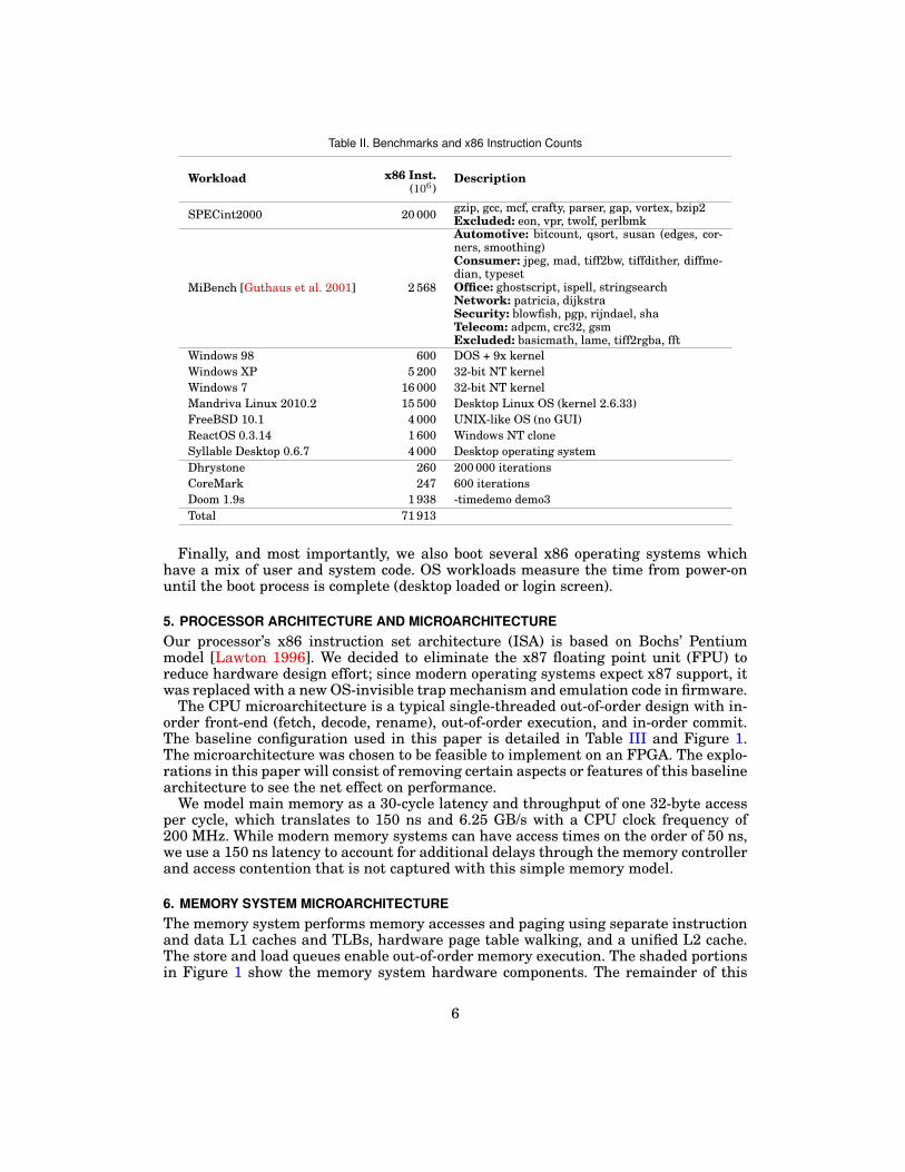
Table II. Benchmarks and x86 Instruction Counts
Workload x86 Inst.(106)
Description
SPECint2000 20 000 gzip, gcc, mcf, crafty, parser, gap, vortex, bzip2Excluded: eon, vpr, twolf, perlbmk
MiBench [Guthaus et al. 2001] 2 568
Automotive: bitcount, qsort, susan (edges, cor-ners, smoothing)Consumer: jpeg, mad, tiff2bw, tiffdither, diffme-dian, typesetOffice: ghostscript, ispell, stringsearchNetwork: patricia, dijkstraSecurity: blowfish, pgp, rijndael, shaTelecom: adpcm, crc32, gsmExcluded: basicmath, lame, tiff2rgba, fft
Windows 98 600 DOS + 9x kernelWindows XP 5 200 32-bit NT kernelWindows 7 16 000 32-bit NT kernelMandriva Linux 2010.2 15 500 Desktop Linux OS (kernel 2.6.33)FreeBSD 10.1 4 000 UNIX-like OS (no GUI)ReactOS 0.3.14 1 600 Windows NT cloneSyllable Desktop 0.6.7 4 000 Desktop operating systemDhrystone 260 200 000 iterationsCoreMark 247 600 iterationsDoom 1.9s 1 938 -timedemo demo3Total 71 913
Finally, and most importantly, we also boot several x86 operating systems whichhave a mix of user and system code. OS workloads measure the time from power-onuntil the boot process is complete (desktop loaded or login screen).
5. PROCESSOR ARCHITECTURE AND MICROARCHITECTUREOur processor’s x86 instruction set architecture (ISA) is based on Bochs’ Pentiummodel [Lawton 1996]. We decided to eliminate the x87 floating point unit (FPU) toreduce hardware design effort; since modern operating systems expect x87 support, itwas replaced with a new OS-invisible trap mechanism and emulation code in firmware.
The CPU microarchitecture is a typical single-threaded out-of-order design with in-order front-end (fetch, decode, rename), out-of-order execution, and in-order commit.The baseline configuration used in this paper is detailed in Table III and Figure 1.The microarchitecture was chosen to be feasible to implement on an FPGA. The explo-rations in this paper will consist of removing certain aspects or features of this baselinearchitecture to see the net effect on performance.
We model main memory as a 30-cycle latency and throughput of one 32-byte accessper cycle, which translates to 150 ns and 6.25 GB/s with a CPU clock frequency of200 MHz. While modern memory systems can have access times on the order of 50 ns,we use a 150 ns latency to account for additional delays through the memory controllerand access contention that is not captured with this simple memory model.
6. MEMORY SYSTEM MICROARCHITECTUREThe memory system performs memory accesses and paging using separate instructionand data L1 caches and TLBs, hardware page table walking, and a unified L2 cache.The store and load queues enable out-of-order memory execution. The shaded portionsin Figure 1 show the memory system hardware components. The remainder of this
6
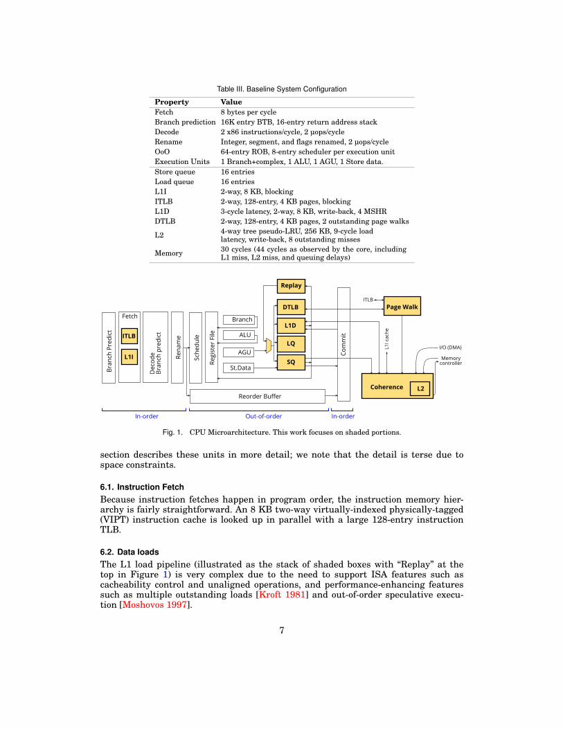
Table III. Baseline System Configuration
Property ValueFetch 8 bytes per cycleBranch prediction 16K entry BTB, 16-entry return address stackDecode 2 x86 instructions/cycle, 2 µops/cycleRename Integer, segment, and flags renamed, 2 µops/cycleOoO 64-entry ROB, 8-entry scheduler per execution unitExecution Units 1 Branch+complex, 1 ALU, 1 AGU, 1 Store data.Store queue 16 entriesLoad queue 16 entriesL1I 2-way, 8 KB, blockingITLB 2-way, 128-entry, 4 KB pages, blockingL1D 3-cycle latency, 2-way, 8 KB, write-back, 4 MSHRDTLB 2-way, 128-entry, 4 KB pages, 2 outstanding page walks
L2 4-way tree pseudo-LRU, 256 KB, 9-cycle loadlatency, write-back, 8 outstanding misses
Memory 30 cycles (44 cycles as observed by the core, includingL1 miss, L2 miss, and queuing delays)
Dec
ode
Bran
chOp
redi
ct
Rena
me
ReorderOBuffer
Sche
dule
Branch
AGU
St.Data
ALU
SQ
LQ
L1D
DTLB
Regi
ster
OFile
Replay
Com
mit
In-order Out-of-order In-order
ITLB
L1I
Bran
chOP
redi
ct
Fetch
Coherence
Page Walk
L2
ITLB
L1IOc
ache
MemoryOcontroller
I/OO)DMA)
Fig. 1. CPU Microarchitecture. This work focuses on shaded portions.
section describes these units in more detail; we note that the detail is terse due tospace constraints.
6.1. Instruction FetchBecause instruction fetches happen in program order, the instruction memory hier-archy is fairly straightforward. An 8 KB two-way virtually-indexed physically-tagged(VIPT) instruction cache is looked up in parallel with a large 128-entry instructionTLB.
6.2. Data loadsThe L1 load pipeline (illustrated as the stack of shaded boxes with “Replay” at thetop in Figure 1) is very complex due to the need to support ISA features such ascacheability control and unaligned operations, and performance-enhancing featuressuch as multiple outstanding loads [Kroft 1981] and out-of-order speculative execu-tion [Moshovos 1997].
7
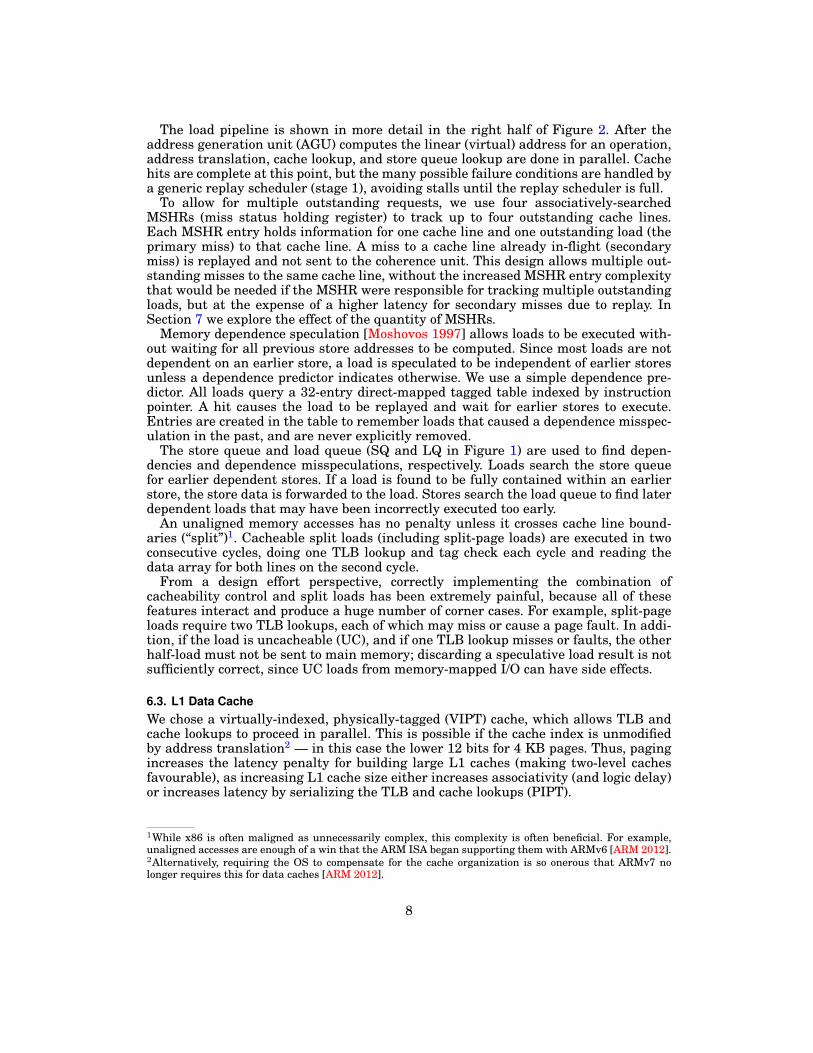
The load pipeline is shown in more detail in the right half of Figure 2. After theaddress generation unit (AGU) computes the linear (virtual) address for an operation,address translation, cache lookup, and store queue lookup are done in parallel. Cachehits are complete at this point, but the many possible failure conditions are handled bya generic replay scheduler (stage 1), avoiding stalls until the replay scheduler is full.
To allow for multiple outstanding requests, we use four associatively-searchedMSHRs (miss status holding register) to track up to four outstanding cache lines.Each MSHR entry holds information for one cache line and one outstanding load (theprimary miss) to that cache line. A miss to a cache line already in-flight (secondarymiss) is replayed and not sent to the coherence unit. This design allows multiple out-standing misses to the same cache line, without the increased MSHR entry complexitythat would be needed if the MSHR were responsible for tracking multiple outstandingloads, but at the expense of a higher latency for secondary misses due to replay. InSection 7 we explore the effect of the quantity of MSHRs.
Memory dependence speculation [Moshovos 1997] allows loads to be executed with-out waiting for all previous store addresses to be computed. Since most loads are notdependent on an earlier store, a load is speculated to be independent of earlier storesunless a dependence predictor indicates otherwise. We use a simple dependence pre-dictor. All loads query a 32-entry direct-mapped tagged table indexed by instructionpointer. A hit causes the load to be replayed and wait for earlier stores to execute.Entries are created in the table to remember loads that caused a dependence misspec-ulation in the past, and are never explicitly removed.
The store queue and load queue (SQ and LQ in Figure 1) are used to find depen-dencies and dependence misspeculations, respectively. Loads search the store queuefor earlier dependent stores. If a load is found to be fully contained within an earlierstore, the store data is forwarded to the load. Stores search the load queue to find laterdependent loads that may have been incorrectly executed too early.
An unaligned memory accesses has no penalty unless it crosses cache line bound-aries (“split”)1. Cacheable split loads (including split-page loads) are executed in twoconsecutive cycles, doing one TLB lookup and tag check each cycle and reading thedata array for both lines on the second cycle.
From a design effort perspective, correctly implementing the combination ofcacheability control and split loads has been extremely painful, because all of thesefeatures interact and produce a huge number of corner cases. For example, split-pageloads require two TLB lookups, each of which may miss or cause a page fault. In addi-tion, if the load is uncacheable (UC), and if one TLB lookup misses or faults, the otherhalf-load must not be sent to main memory; discarding a speculative load result is notsufficiently correct, since UC loads from memory-mapped I/O can have side effects.
6.3. L1 Data CacheWe chose a virtually-indexed, physically-tagged (VIPT) cache, which allows TLB andcache lookups to proceed in parallel. This is possible if the cache index is unmodifiedby address translation2 — in this case the lower 12 bits for 4 KB pages. Thus, pagingincreases the latency penalty for building large L1 caches (making two-level cachesfavourable), as increasing L1 cache size either increases associativity (and logic delay)or increases latency by serializing the TLB and cache lookups (PIPT).
1While x86 is often maligned as unnecessarily complex, this complexity is often beneficial. For example,unaligned accesses are enough of a win that the ARM ISA began supporting them with ARMv6 [ARM 2012].2Alternatively, requiring the OS to compensate for the cache organization is so onerous that ARMv7 nolonger requires this for data caches [ARM 2012].
8
L1D Load
ReplayAGU
TLB Tag DataMSHR
=
Writeback
Reg.File
Schedule
LQ
Arbitrate
L1DTagL1ITagL2Tag
Cache1miss
L1D1DataL21DataL1I1Datato pgwk
L1D1DataL21Data
Data1source1mux
L1DL1IPgwkFillSnoop ...Q
ueue
sTa
g ch
eck
Read
Dat
aD
rive
Wri
teD
ata
Coherence + L2
SQ
1
2
3
4
1
2
3
4
5
6
256
256256256
32 32
256 256256 256
32
32256 256
Fig. 2. Load and Coherence Pipeline Diagram. 3-cycle L1D hit latency, 9-cycle L2 hit latency.
6.4. Coherence Unit and L2 CacheThe coherence unit merges requests from 8 sources, most of which are shown in theleft hand side of Figure 2: L1D loads, L1D stores, L1D evictions, L1I reads, page tablewalker, memory fill, I/O device-initiated requests (DMA), and I/O-space requests. Thecoherence unit services requests, maintains coherence of all caches, and provides aglobal ordering to satisfy memory consistency requirements.
The L2 cache uses a non-inclusive/non-exclusive (“accidental inclusion”) policy, so allL1 cache tags are checked at every request. A second copy of all L1 cache tag arraysis used for this purpose. A non-inclusive policy reduces complexity compared to aninclusive policy by avoiding reverse invalidations when the L2 wishes to evict a linethat is also stored in at least one L1 cache.
6.5. TLB and Page Table WalkerThe instruction and data TLBs are both 128-entry, two-way set-associative. Althoughprocessors have often used higher-associativity or fully-associative TLBs, we believelow-associativity TLBs are more suitable for FPGA processors. First, storage capacityis reasonably cheap, so it is easier to reduce miss rates by increasing capacity ratherthan associativity. Increasing cache capacity also reduces sensitivity to associativity.Our large 128-entry L1 data TLB loses less than 1% IPC for two-way associativityfor SPECint2000. Second, using a low-associativity TLB and cache allows cache tagcomparisons to be overlapped with TLB tag comparisons, which has a large circuitspeed advantage, which we discuss in Section 9. Serializing the tag comparisons toaccommodate a higher-associativity (or fully-associative) TLB in the same latency and
9
Core
mar
kD
hrys
tone
Doo
m
Win
98W
inXP
Win
7Li
nux
Free
BSD
Reac
tOS
Sylla
ble
OS
GEO
MEA
N
ADPC
M E
ncod
eAD
PCM
Dec
ode
bitc
ount
Blow
fish
enco
deBl
owfis
h de
code
CRC3
2di
jkst
raG
host
scri
ptG
SM E
ncod
eG
SM D
ecod
eis
pell
JPEG
MAD
patr
icia
PGP
sign
PGP
veri
fyqs
ort
rijn
dael
enc
ode
rijn
dael
dec
ode
sha
stri
ngse
arch
susa
n (c
orne
rs)
susa
n (e
dges
)su
san
(sm
ooth
ing)
tiff2
bwtif
fdith
ertif
fmed
ian
type
set
Mib
ench
GEO
MEA
N
bzip
2cr
afty
gap
gcc
gzip
mcf
pars
ervo
rtex
SPEC
GEO
MEA
N
0.00
0.20
0.40
0.60
0.80
1.00
1.20
1.40
0.87
1.20
0.84
0.40
0.58 0.59
0.76
0.69
0.620.68
0.61
0.92 0.91
1.03
0.93 0.94
1.26
1.19
1.01 1.010.95
0.69
0.92 0.94
0.800.78
0.87
0.71
1.191.15
1.24
0.85
0.79 0.800.86
0.61
0.95
0.79
0.70
0.91 0.88
0.75
1.05
0.55
0.87
0.30
0.72
0.83
0.70
0.82
1.11
0.76
0.37
0.540.49
0.65 0.62
0.53
0.61
0.54
0.810.86
1.00
0.82 0.83
1.101.06
0.940.88
0.83
0.60
0.73 0.74 0.760.73
0.83
0.64
0.84 0.81
0.94
0.82
0.72 0.74 0.75
0.55
0.85
0.62 0.62
0.79
0.69 0.700.75
0.35
0.74
0.16
0.59
0.74
0.53
0.81
1.10
0.59
0.23
0.370.34
0.41 0.400.37 0.40
0.35
0.74
0.83
0.99
0.700.73
1.02
0.71
0.54
0.69 0.67
0.48
0.620.58
0.29
0.57
0.72
0.520.55 0.57
0.86
0.64
0.48 0.47
0.59
0.33
0.78
0.40
0.31
0.59
0.49
0.22
0.61
0.27
0.55
0.11
0.38
0.31 0.33
Out-of-order non-blockingIn-order blockingIn-order blocking, no L2
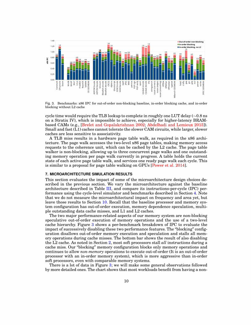
x86
IPC
Fig. 3. Benchmarks: x86 IPC for out-of-order non-blocking baseline, in-order blocking cache, and in-orderblocking without L2 cache
cycle time would require the TLB lookup to complete in roughly one LUT delay (∼0.8 nson a Stratix IV), which is impossible to achieve, especially for higher-latency BRAM-based CAMs (e.g., [Brelet and Gopalakrishnan 2002; Abdelhadi and Lemieux 2015]).Small and fast (L1) caches cannot tolerate the slower CAM circuits, while larger, slowercaches are less sensitive to associativity.
A TLB miss results in a hardware page table walk, as required in the x86 archi-tecture. The page walk accesses the two-level x86 page tables, making memory accessrequests to the coherence unit, which can be cached by the L2 cache. The page tablewalker is non-blocking, allowing up to three concurrent page walks and one outstand-ing memory operation per page walk currently in progress. A table holds the currentstate of each active page table walk, and services one ready page walk each cycle. Thisis similar to a proposal for page table walking on GPUs [Power et al. 2014].
7. MICROARCHITECTURE SIMULATION RESULTSThis section evaluates the impact of some of the microarchitecture design choices de-scribed in the previous section. We vary the microarchitecture against the baselinearchitecture described in Table III, and compare its instructions-per-cycle (IPC) per-formance using the cycle-level simulator and benchmarks described in Section 4. Notethat we do not measure the microarchitectural impact on frequency and area yet, butleave those results to Section 10. Recall that the baseline processor and memory sys-tem configuration has out-of-order execution, memory dependence speculation, multi-ple outstanding data cache misses, and L1 and L2 caches.
The two major performance-related aspects of our memory system are non-blockingspeculative out-of-order execution of memory operations and the use of a two-levelcache hierarchy. Figure 3 shows a per-benchmark breakdown of IPC to evaluate theimpact of successively disabling these two performance features. The “blocking” config-uration disallows out-of-order memory execution and speculation and stalls all mem-ory operations during cache misses. The bottom bar shows the result of also disablingthe L2 cache. As noted in Section 2, most soft processors stall all instructions during acache miss. Our “blocking” memory configuration blocks only memory operations andcontinues to allow non-memory operations to execute out-of-order (It is an out-of-orderprocessor with an in-order memory system), which is more aggressive than in-ordersoft processors, even with comparable memory systems.
There is a lot of data in Figure 3; we will make some general observations followedby more detailed ones. The chart shows that most workloads benefit from having a non-
10
blocking cache, particularly those with large working sets (e.g., SPECint’s mcf [Jaleel2007]). Workloads with very small working sets (Coremark, Dhrystone) show no sen-sitivity to removing the L2 cache, but still benefit from out-of-order execution of cachehits. Overall, the benefit of a two-level non-blocking memory system are large (2.1×IPC on SPECint2000). These large gains are seen even with our modest two-issue pro-cessor and the smaller memory latencies seen on lower-clock speed FPGA processors.
The rest of this section looks at the benefits of non-blocking caches and a two-levelcache hierarchy in more detail.
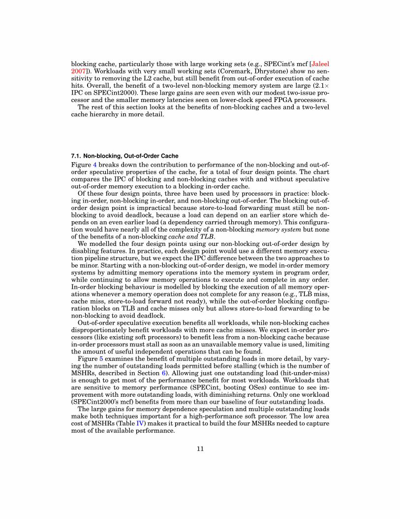
7.1. Non-blocking, Out-of-Order CacheFigure 4 breaks down the contribution to performance of the non-blocking and out-of-order speculative properties of the cache, for a total of four design points. The chartcompares the IPC of blocking and non-blocking caches with and without speculativeout-of-order memory execution to a blocking in-order cache.
Of these four design points, three have been used by processors in practice: block-ing in-order, non-blocking in-order, and non-blocking out-of-order. The blocking out-of-order design point is impractical because store-to-load forwarding must still be non-blocking to avoid deadlock, because a load can depend on an earlier store which de-pends on an even earlier load (a dependency carried through memory). This configura-tion would have nearly all of the complexity of a non-blocking memory system but noneof the benefits of a non-blocking cache and TLB.
We modelled the four design points using our non-blocking out-of-order design bydisabling features. In practice, each design point would use a different memory execu-tion pipeline structure, but we expect the IPC difference between the two approaches tobe minor. Starting with a non-blocking out-of-order design, we model in-order memorysystems by admitting memory operations into the memory system in program order,while continuing to allow memory operations to execute and complete in any order.In-order blocking behaviour is modelled by blocking the execution of all memory oper-ations whenever a memory operation does not complete for any reason (e.g., TLB miss,cache miss, store-to-load forward not ready), while the out-of-order blocking configu-ration blocks on TLB and cache misses only but allows store-to-load forwarding to benon-blocking to avoid deadlock.
Out-of-order speculative execution benefits all workloads, while non-blocking cachesdisproportionately benefit workloads with more cache misses. We expect in-order pro-cessors (like existing soft processors) to benefit less from a non-blocking cache becausein-order processors must stall as soon as an unavailable memory value is used, limitingthe amount of useful independent operations that can be found.
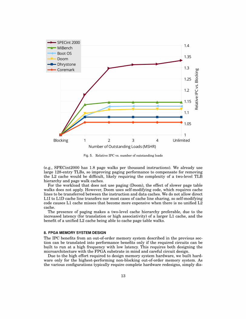
Figure 5 examines the benefit of multiple outstanding loads in more detail, by vary-ing the number of outstanding loads permitted before stalling (which is the number ofMSHRs, described in Section 6). Allowing just one outstanding load (hit-under-miss)is enough to get most of the performance benefit for most workloads. Workloads thatare sensitive to memory performance (SPECint, booting OSes) continue to see im-provement with more outstanding loads, with diminishing returns. Only one workload(SPECint2000’s mcf) benefits from more than our baseline of four outstanding loads.
The large gains for memory dependence speculation and multiple outstanding loadsmake both techniques important for a high-performance soft processor. The low areacost of MSHRs (Table IV) makes it practical to build the four MSHRs needed to capturemost of the available performance.
11
Dhrystone Coremark Doom MiBench SPECint 2000 Boot OS0.9
0.95
1
1.05
1.1
1.15
1.2
1.25
1.3
1.35
1.081.06
1.04
1.131.10
1.06
1.01 1.01
1.061.05
1.21
1.081.081.06
1.11
1.15
1.32
1.13
Blocking, In-order memoryBlocking, Out-of-Order memoryNon-blocking, In-order memoryNon-blocking, Out-of-order memory
Rela
tive
IPC
vs. I
n-or
der B
lock
ing
Fig. 4. IPC impact of non-blocking and out-of-order memory execution (256 KB L2, 4 MSHR entries). Ablocking out-of-order memory system is an impractical design. Pink and dark green bars correspond to barsof the same colour in Figure 3.
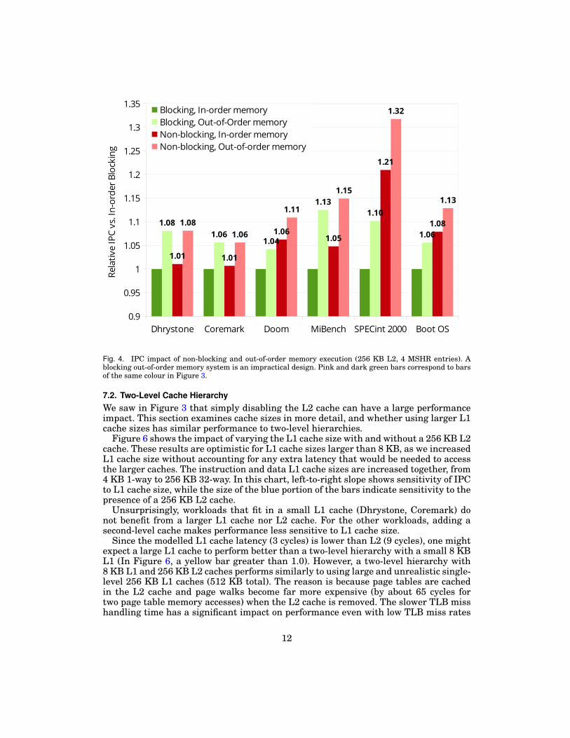
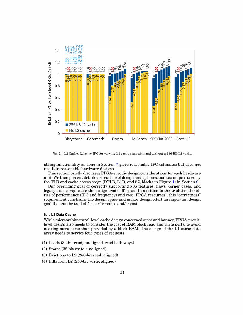
7.2. Two-Level Cache HierarchyWe saw in Figure 3 that simply disabling the L2 cache can have a large performanceimpact. This section examines cache sizes in more detail, and whether using larger L1cache sizes has similar performance to two-level hierarchies.
Figure 6 shows the impact of varying the L1 cache size with and without a 256 KB L2cache. These results are optimistic for L1 cache sizes larger than 8 KB, as we increasedL1 cache size without accounting for any extra latency that would be needed to accessthe larger caches. The instruction and data L1 cache sizes are increased together, from4 KB 1-way to 256 KB 32-way. In this chart, left-to-right slope shows sensitivity of IPCto L1 cache size, while the size of the blue portion of the bars indicate sensitivity to thepresence of a 256 KB L2 cache.
Unsurprisingly, workloads that fit in a small L1 cache (Dhrystone, Coremark) donot benefit from a larger L1 cache nor L2 cache. For the other workloads, adding asecond-level cache makes performance less sensitive to L1 cache size.
Since the modelled L1 cache latency (3 cycles) is lower than L2 (9 cycles), one mightexpect a large L1 cache to perform better than a two-level hierarchy with a small 8 KBL1 (In Figure 6, a yellow bar greater than 1.0). However, a two-level hierarchy with8 KB L1 and 256 KB L2 caches performs similarly to using large and unrealistic single-level 256 KB L1 caches (512 KB total). The reason is because page tables are cachedin the L2 cache and page walks become far more expensive (by about 65 cycles fortwo page table memory accesses) when the L2 cache is removed. The slower TLB misshandling time has a significant impact on performance even with low TLB miss rates
12
Unlimited4321Blocking1
1.05
1.1
1.15
1.2
1.25
1.3
1.35
1.4SPECint 2000MiBenchBoot OSDoomDhrystoneCoremark
Number of Outstanding Loads (MSHR)
Rela
tive
IPC
vs. B
lock
ing
Fig. 5. Relative IPC vs. number of outstanding loads
(e.g., SPECint2000 has 1.8 page walks per thousand instructions). We already uselarge 128-entry TLBs, so improving paging performance to compensate for removingthe L2 cache would be difficult, likely requiring the complexity of a two-level TLBhierarchy and page walk caches.
For the workload that does not use paging (Doom), the effect of slower page tablewalks does not apply. However, Doom uses self-modifying code, which requires cachelines to be transferred between the instruction and data caches. We do not allow directL1I to L1D cache line transfers nor most cases of cache line sharing, so self-modifyingcode causes L1 cache misses that become more expensive when there is no unified L2cache.
The presence of paging makes a two-level cache hierarchy preferable, due to theincreased latency (for translation or high associativity) of a larger L1 cache, and thebenefit of a unified L2 cache being able to cache page table walks.
8. FPGA MEMORY SYSTEM DESIGNThe IPC benefits from an out-of-order memory system described in the previous sec-tion can be translated into performance benefits only if the required circuits can bebuilt to run at a high frequency with low latency. This requires both designing themicroarchitecture with the FPGA substrate in mind and careful circuit design.
Due to the high effort required to design memory system hardware, we built hard-ware only for the highest-performing non-blocking out-of-order memory system. Asthe various configurations typically require complete hardware redesigns, simply dis-
13
Dhrystone Coremark Doom MiBench SPECint 2000 Boot OS
1.00
1.00
0.97
0.93
0.93 0.951.00
1.00
1.00
1.00
1.00
1.00
1.00
1.00
1.01 1.02 1.05
1.03
1.00
1.00 1.02 1.04 1.
07
1.05
1.00
1.00 1.
04
1.05 1.
09
1.06
1.00
1.00 1.
05
1.05 1.
11
1.08
1.00
1.00
1.09
1.06 1.
13
1.10
Rela
tive
IPC
vs T
wo-
leve
l 8 K
B/25
6 KB
0
0.2
0.4
0.6
0.8
1
1.2
1.4
0.99
0.94
0.62
0.52
0.46 0.
52
0.99
0.99
0.81
0.75
0.60 0.
65
1.00
1.00
0.86 0.88
0.74 0.
77
1.00
1.00
0.88
0.97
0.85 0.87
1.00
1.00
0.91
1.01
0.91 0.931.
00
1.00
0.93
1.03
0.94 0.
981.00
1.00
1.00 1.
04
0.97 1.
00
256 KB L2 cacheNo L2 cache
4 KB
1-w
ay8
KB2-
way
16 K
B4-
way
32 K
B8-
way
64 K
B16
-way
128
KB32
-way
256
KB32
-way
Fig. 6. L2 Cache: Relative IPC for varying L1 cache sizes with and without a 256 KB L2 cache.
abling functionality as done in Section 7 gives reasonable IPC estimates but does notresult in reasonable hardware designs.
This section briefly discusses FPGA-specific design considerations for each hardwareunit. We then present detailed circuit-level design and optimization techniques used bythe TLB and cache access stage (DTLB, L1D, and SQ blocks in Figure 1) in Section 9.
Our overriding goal of correctly supporting x86 features, flaws, corner cases, andlegacy code complicates the design trade-off space. In addition to the traditional met-rics of performance (IPC and frequency) and cost (FPGA resources), this “correctness”requirement constrains the design space and makes design effort an important designgoal that can be traded for performance and/or cost.
8.1. L1 Data CacheWhile microarchitectural-level cache design concerned sizes and latency, FPGA circuit-level design also needs to consider the cost of RAM block read and write ports, to avoidneeding more ports than provided by a block RAM. The design of the L1 cache dataarray needs to service four types of requests:
(1) Loads (32-bit read, unaligned, read both ways)(2) Stores (32-bit write, unaligned)(3) Evictions to L2 (256-bit read, aligned)(4) Fills from L2 (256-bit write, aligned)
14
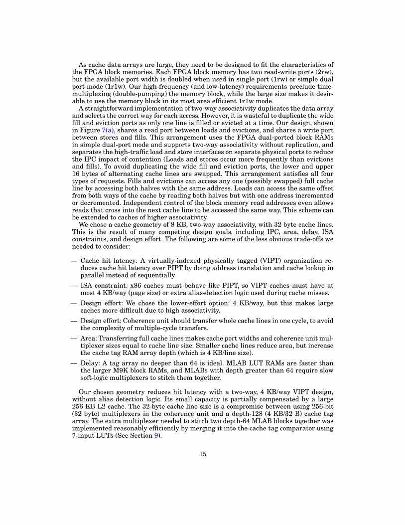
As cache data arrays are large, they need to be designed to fit the characteristics ofthe FPGA block memories. Each FPGA block memory has two read-write ports (2rw),but the available port width is doubled when used in single port (1rw) or simple dualport mode (1r1w). Our high-frequency (and low-latency) requirements preclude time-multiplexing (double-pumping) the memory block, while the large size makes it desir-able to use the memory block in its most area efficient 1r1w mode.
A straightforward implementation of two-way associativity duplicates the data arrayand selects the correct way for each access. However, it is wasteful to duplicate the widefill and eviction ports as only one line is filled or evicted at a time. Our design, shownin Figure 7(a), shares a read port between loads and evictions, and shares a write portbetween stores and fills. This arrangement uses the FPGA dual-ported block RAMsin simple dual-port mode and supports two-way associativity without replication, andseparates the high-traffic load and store interfaces on separate physical ports to reducethe IPC impact of contention (Loads and stores occur more frequently than evictionsand fills). To avoid duplicating the wide fill and eviction ports, the lower and upper16 bytes of alternating cache lines are swapped. This arrangement satisfies all fourtypes of requests. Fills and evictions can access any one (possibly swapped) full cacheline by accessing both halves with the same address. Loads can access the same offsetfrom both ways of the cache by reading both halves but with one address incrementedor decremented. Independent control of the block memory read addresses even allowsreads that cross into the next cache line to be accessed the same way. This scheme canbe extended to caches of higher associativity.
We chose a cache geometry of 8 KB, two-way associativity, with 32 byte cache lines.This is the result of many competing design goals, including IPC, area, delay, ISAconstraints, and design effort. The following are some of the less obvious trade-offs weneeded to consider:
— Cache hit latency: A virtually-indexed physically tagged (VIPT) organization re-duces cache hit latency over PIPT by doing address translation and cache lookup inparallel instead of sequentially.
— ISA constraint: x86 caches must behave like PIPT, so VIPT caches must have atmost 4 KB/way (page size) or extra alias-detection logic used during cache misses.
— Design effort: We chose the lower-effort option: 4 KB/way, but this makes largecaches more difficult due to high associativity.
— Design effort: Coherence unit should transfer whole cache lines in one cycle, to avoidthe complexity of multiple-cycle transfers.
— Area: Transferring full cache lines makes cache port widths and coherence unit mul-tiplexer sizes equal to cache line size. Smaller cache lines reduce area, but increasethe cache tag RAM array depth (which is 4 KB/line size).
— Delay: A tag array no deeper than 64 is ideal. MLAB LUT RAMs are faster thanthe larger M9K block RAMs, and MLABs with depth greater than 64 require slowsoft-logic multiplexers to stitch them together.
Our chosen geometry reduces hit latency with a two-way, 4 KB/way VIPT design,without alias detection logic. Its small capacity is partially compensated by a large256 KB L2 cache. The 32-byte cache line size is a compromise between using 256-bit(32 byte) multiplexers in the coherence unit and a depth-128 (4 KB/32 B) cache tagarray. The extra multiplexer needed to stitch two depth-64 MLAB blocks together wasimplemented reasonably efficiently by merging it into the cache tag comparator using7-input LUTs (See Section 9).
15
set0Away0A[127:0]
set0Away1A[127:0]
set0Away0A[255:128]
set0Away1A[255:128]
set1Away0A[127:0]
set1Away1A[127:0]
set1Away0A[255:128]
set1Away1A[255:128]
Evict
swap
offset offset
wayAselect
offset
swap
storeAorAfill
Store data
... ...
shift-16 shift-164 4
128 128
32 32
256
256Fill
storeAorAfill
2
32
Load data
Dat
aARA
MA2
56x2
56b
32
(a) Data Cache
set0hway0h[127:0]
set0hway1h[127:0]
set0hway0h[255:128]
set0hway1h[255:128]
set1hway0h[127:0]
set1hway1h[127:0]
set1hway0h[255:128]
set1hway1h[255:128]
swap... ...
64 64
256Fill
Fetch data
Dat
ahRA
Mh(m
ixed
hpor
thwid
th)h
Wri
te:h2
56x2
56b
Read
:h512
x128
b
wayhselect
64
(b) Instruction Cache
Fig. 7. L1 Cache Data RAM Arrays and Interleaving
8.2. L1 Instruction CacheThe L1 instruction cache, shown in Figure 7(b), is derived from the data cache, with thesame VIPT structure. Since the instruction cache is read-only, it omits the store portand eviction port. It also does not need to support unaligned reads, as all instructionfetches are aligned 8-byte reads. Thus, the instruction cache only has load and fillinterfaces, and can use mixed port widths to reduce multiplexing.
8.3. Coherence Unit and L2 cacheAs shown in Figure 2, the coherence unit has many data paths that connect the outputof block RAMs to the input of other block RAMs. This occurs both for tag checks feedingthe data array’s read address, and to allow copying a cache line from one cache toanother. Due to the block memories’ large setup times, long read latency, and routingdelay, these paths have been problematic for delay. To mitigate this, there are two
16
address[uu)M]
size[u)M]
nng
ngn
validLNLolder
[uu]
[uu]
MLAB
way
LMse
tLMg5
/
MLAB
way
LMse
tL5mg
uxH
MLAB
way
Luse
tLMg5
/
MLAB
way
Luse
tL5mg
uxH
LoadDdata[5-:6]
Select
Cache2hit2way21?
TLB2hit2way20?
Way
D6Dt
agDm
atch
DORD
bypa
ssDt
rans
lati
on
TLBDtagDcompare CacheDtagDcompare DataDselectStoreDqueueDCAMDsearch
address[uu)M]
size[u)M]
nng
ngn
validLNLolder
[uu]
[uu]
size
[u)M
]
SQ
2ma
tch
?
DTLBVFNLwayLM
DTLBPFNLwayLu
MLAB MLAB
CacheDtags
A[xM
)uR]
VFN
[xM)
uR]
=?
6-LUT
A[x(
)xH]
VFN
[x()
xH]
=?
6-LUT
CCC
A[/u
)/M]
VFN
[/u)
/M]
=?
5-LUT
VFN
Lval
id
bypassLaddresstranslation
6-LUT
Way
D-Dt
agDm
atch
DAN
DN
OTD
bypa
ssDt
rans
lati
on
DTLBVFNLwayLu
MLAB
PFN
[u/)
ux]
tagL
[u/)
ux]
=?
7-LUT
tagH
[u/)
ux]
CCCxD-6
5-LUT 5-LUT
Cach
eDw
ayD6
Dtag
Dmat
chDP
FNDw
ayD6
Cach
eDw
ayD6
Dtag
Dmat
chDA
[5-:
-Q]
Cach
eDw
ayD6
Dtag
Dmat
chDP
FNDw
ayD-
Cach
eDw
ayD-
Dtag
Dmat
chDP
FNDw
ayD-
Cach
eDw
ayD-
Dtag
Dmat
chDP
FNDw
ayD6
Cach
eDw
ayD-
Dtag
Dmat
chDA
[5-:
-Q]
bypa
ssLa
ddre
sstr
ansl
atio
n
7-LUT
CacheLdata
8x2M9K
MuxLselect
[/)M
]
Select
32x25-LUT
CacheLhithmiss
L H L H
A[/u
)uR]
CCC
-6xentryDstoreDqueue
SQDentryD-E
SQDentryD-4
A[uu
)M]
PFN
[/u)
/M]
tagL
[/u)
/M]
=?
7-LUT
tagH
[/u)
/M]
A[uu
]
6-LUT
StatushithmissPLetcC
mCx5Lns
mCu(Lns
mCu5Lns
mCx(LnsmCu/Lns
Entr
yD-
Entr
yD6
DTLBPFNLwayLM
MLAB
A[m)
M]
x,5
/x /x
FromLmgentryLMSHRLsearch.notLshownb
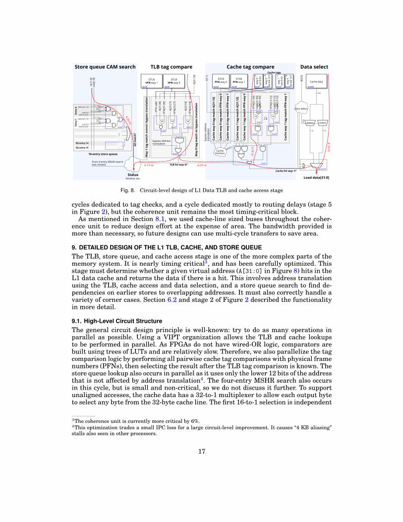
Fig. 8. Circuit-level design of L1 Data TLB and cache access stage
cycles dedicated to tag checks, and a cycle dedicated mostly to routing delays (stage 5in Figure 2), but the coherence unit remains the most timing-critical block.
As mentioned in Section 8.1, we used cache-line sized buses throughout the coher-ence unit to reduce design effort at the expense of area. The bandwidth provided ismore than necessary, so future designs can use multi-cycle transfers to save area.
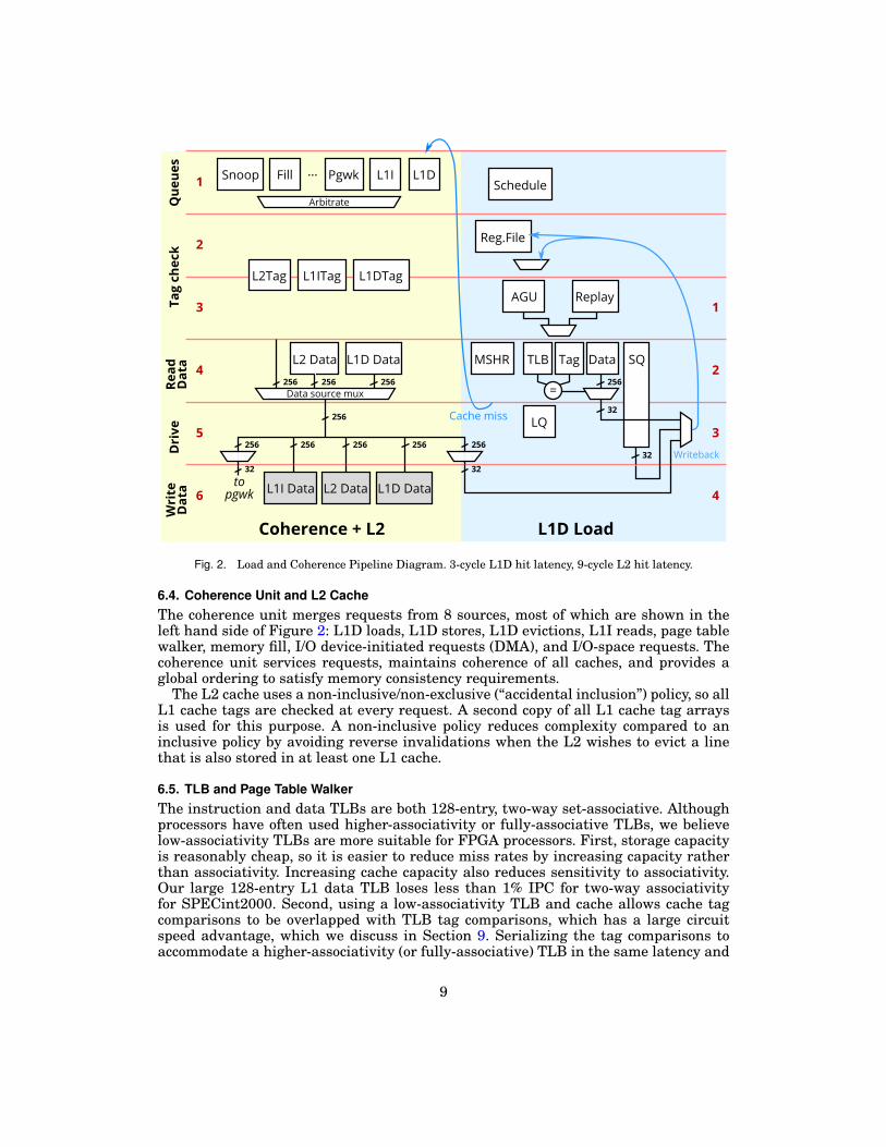
9. DETAILED DESIGN OF THE L1 TLB, CACHE, AND STORE QUEUEThe TLB, store queue, and cache access stage is one of the more complex parts of thememory system. It is nearly timing critical3, and has been carefully optimized. Thisstage must determine whether a given virtual address (A[31:0] in Figure 8) hits in theL1 data cache and returns the data if there is a hit. This involves address translationusing the TLB, cache access and data selection, and a store queue search to find de-pendencies on earlier stores to overlapping addresses. It must also correctly handle avariety of corner cases. Section 6.2 and stage 2 of Figure 2 described the functionalityin more detail.
9.1. High-Level Circuit StructureThe general circuit design principle is well-known: try to do as many operations inparallel as possible. Using a VIPT organization allows the TLB and cache lookupsto be performed in parallel. As FPGAs do not have wired-OR logic, comparators arebuilt using trees of LUTs and are relatively slow. Therefore, we also parallelize the tagcomparison logic by performing all pairwise cache tag comparisons with physical framenumbers (PFNs), then selecting the result after the TLB tag comparison is known. Thestore queue lookup also occurs in parallel as it uses only the lower 12 bits of the addressthat is not affected by address translation4. The four-entry MSHR search also occursin this cycle, but is small and non-critical, so we do not discuss it further. To supportunaligned accesses, the cache data has a 32-to-1 multiplexer to allow each output byteto select any byte from the 32-byte cache line. The first 16-to-1 selection is independent
3The coherence unit is currently more critical by 6%.4This optimization trades a small IPC loss for a large circuit-level improvement. It causes “4 KB aliasing”stalls also seen in other processors.
17
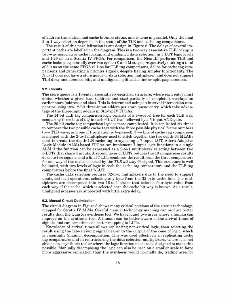
of address translation and cache hit/miss status, and is done in parallel. Only the final2-to-1 way selection depends on the result of the TLB and cache tag comparisons.
The result of this parallelization is our design in Figure 8. The delays of several im-portant paths are labelled on the diagram. This is a two-way associative TLB lookup, atwo-way associative cache lookup, and unaligned data selection, in 5 LUT logic levelsand 4.29 ns on a Stratix IV FPGA. For comparison, the Nios II/f performs TLB andcache lookup sequentially over two cycles (E and M stages, respectively), taking a totalof 6.0 ns on the same FPGA (2.1 ns for TLB tag comparisons, 3.9 ns for cache tag com-parisons and generating a hit/miss signal), despite having simpler functionality. TheNios II does not have a store queue or data selection multiplexer, and does not supportTLB dirty and accessed bits, and unaligned, split-cache line or split-page accesses.
9.2. CircuitsThe store queue is a 16-entry associatively-searched structure, where each entry mustdecide whether a given load (address and size) partially or completely overlaps anearlier store (address and size). This is determined using an interval-intersection com-parator using two 12-bit three-input adders per store queue entry, which take advan-tage of the three-input adders in Stratix IV FPGAs.
The 14-bit TLB tag comparison logic consists of a two-level tree for each TLB way,comparing three bits of tag in each 6-LUT leaf, followed by a 5-input AND gate.
The 20-bit cache tag comparison logic is more complicated. It is replicated six timesto compare the two possible cache tags with the three possible physical frame numbers(two TLB ways, and one if translation is bypassed). Two bits of cache tag comparisonis merged with the 2-to-1 multiplexer used to stitch together the two depth-64 MLABsused to create the depth-128 cache tag array, using a 7-input LUT. Altera AdaptiveLogic Module (ALM)-based FPGAs can implement 7-input logic functions in a singleALM if the function can be expressed as a 2-to-1 multiplexer selecting between two5-LUTs that share 4 inputs. A second layer of LUTs reduces the 10 comparison resultsdown to two signals, and a final 7-LUT combines the result from the three comparatorsfor one way of the cache, selected by the TLB hit way 0? signal. This structure is wellbalanced, with two levels of logic in both the cache tag comparators and the TLB tagcomparators before the final 7-LUT.
The cache data selection requires 32-to-1 multiplexers due to the need to supportunaligned load operations, selecting any byte from the 32-byte cache line. The mul-tiplexers are decomposed into two 16-to-1 blocks that select a four-byte value fromeach way of the cache, which is selected once the cache hit way is known. As a result,unaligned accesses are supported with little extra delay.
9.3. Manual Circuit OptimizationThe circuit diagram in Figure 8 shows many critical portions of the circuit technology-mapped for Stratix IV ALMs. Careful manual technology mapping can produce betterresults than the Quartus synthesis tool. We have found two areas where a human canimprove on the synthesis tool: A human can be better aware of the arrival times ofsignals, and can sometimes do better mapping to LUTs.
Knowledge of arrival times allows replicating non-critical logic, then selecting theresult using the late-arriving signal nearer to the output of the cone of logic, whichis essentially Shannon decomposition. This was used effectively in replicating cachetag comparators and in restructuring the data selection multiplexers, where it is notobvious to a synthesis tool or where the logic function needs to be designed to make thispossible. Manually decomposing the logic can also be used on a smaller scale to forcemore aggressive replication than the synthesis would normally do, trading area for
18
performance. The keep synthesis attribute prevents the synthesis tool from optimizingaway the manual duplication.
More control over mapping to LUTs can be accomplished by using the keep directiveto delimit LUT boundaries, or using LCELL buffers, depending on which syntax is moreconvenient. However, in many cases involving 7-LUTs, the synthesizer refuses to cre-ate them even with clear boundaries, and we had to resort to using low-level deviceprimitives, which Altera calls “WYSIWYG” primitives.
The keep attribute can also be used to push non-critical logic further up a logic coneto reduce the size of the final critical LUT. This was used to keep the final stage of thedata selection multiplexers no larger than a 5-LUT, which is slightly faster than if thesynthesizer were allowed to combine some non-critical signals into a larger LUT.
The impact of the above manual optimizations can be approximately measured byremoving the keep attributes and instructing Quartus synthesis to allow resynthe-sis of LCELL buffers and WYSIWYG primitives. This is an inexact comparison, asthe desired circuit structure is still obvious in the code, rather than the typical sce-nario where the synthesis tool must infer technology-dependent circuit structures fromtechnology-independent behavioural RTL code.
With manual optimizations resynthesized away, the delay of the cache access stageincreased from 4.29 ns to 4.87 ns (13.5%), due to an increase from 5 logic levels to7 (best of 30 placement random seeds). Both the TLB and cache tag comparison logicincreased by one logic level. A second increase occurred in the data selection multiplex-ers, as Quartus synthesis did not place the most critical signal nearest the output ofthe cone of logic. Manual optimizations increased ALM usage by a negligible 68 ALMs(0.5%).
Overall, the synthesis tools work well for non-critical paths, and manual mappingto LUTs is only necessary in critical regions where the synthesized circuit structureis sub-optimal. However, being aware of technology mapping during microarchitecturedesign can enable new circuit-level optimizations and allow verifying the synthesizedoutput’s circuit structure.
10. FPGA MEMORY SYSTEM IMPLEMENTATION RESULTSWe completed the full design of the baseline configuration of the memory system (de-scribed in Table III) and synthesized it on an Altera Stratix IV FPGA (smallest chip,fastest speed grade, EP4SGX70HF35C2), using Quartus 15.0.
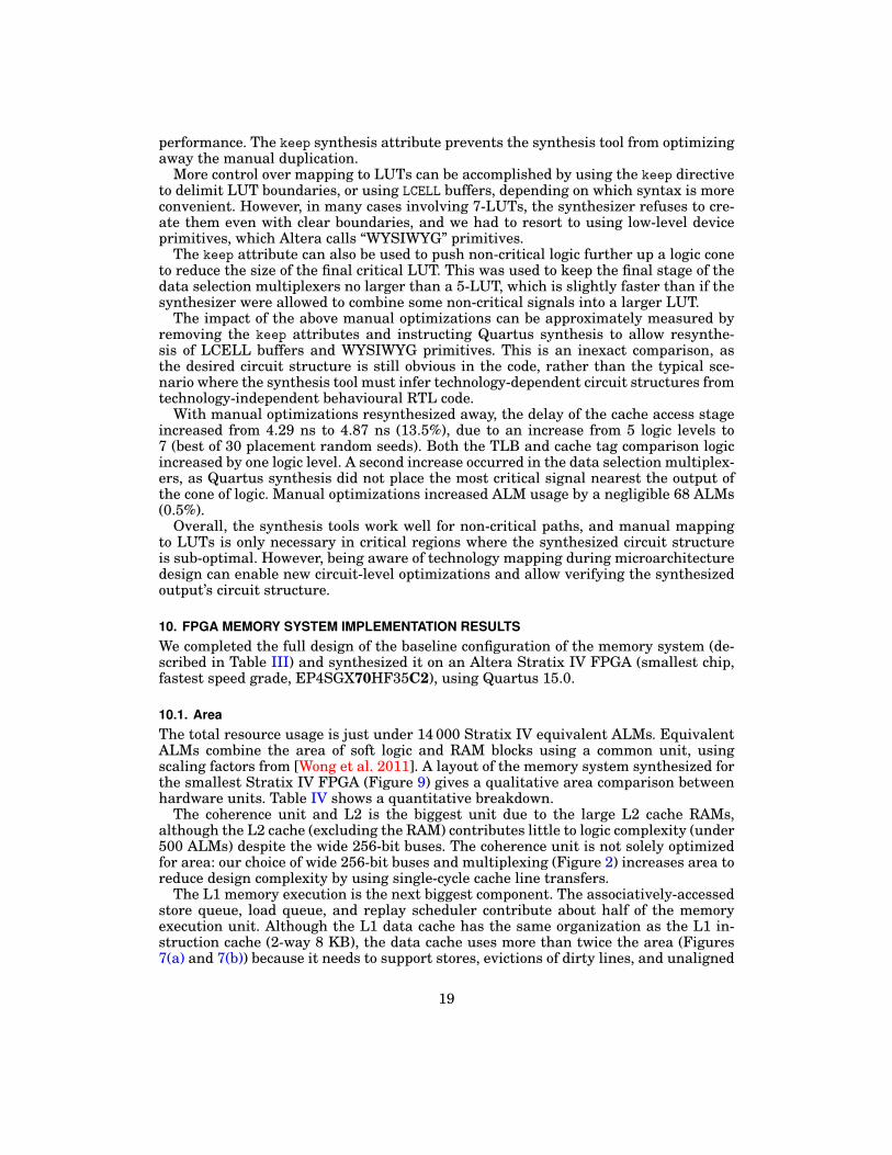
10.1. AreaThe total resource usage is just under 14 000 Stratix IV equivalent ALMs. EquivalentALMs combine the area of soft logic and RAM blocks using a common unit, usingscaling factors from [Wong et al. 2011]. A layout of the memory system synthesized forthe smallest Stratix IV FPGA (Figure 9) gives a qualitative area comparison betweenhardware units. Table IV shows a quantitative breakdown.
The coherence unit and L2 is the biggest unit due to the large L2 cache RAMs,although the L2 cache (excluding the RAM) contributes little to logic complexity (under500 ALMs) despite the wide 256-bit buses. The coherence unit is not solely optimizedfor area: our choice of wide 256-bit buses and multiplexing (Figure 2) increases area toreduce design complexity by using single-cycle cache line transfers.
The L1 memory execution is the next biggest component. The associatively-accessedstore queue, load queue, and replay scheduler contribute about half of the memoryexecution unit. Although the L1 data cache has the same organization as the L1 in-struction cache (2-way 8 KB), the data cache uses more than twice the area (Figures7(a) and 7(b)) because it needs to support stores, evictions of dirty lines, and unaligned
19
Load/storePexecution128-entryPP2-wayPTLB8PKBP2-wayPcache
16-entryPLoadPqueue16-entryPStorePqueue8-entryPscheduler
InstructionPFetch128-entryPP2-wayPTLB8PKBP2-wayPcache
PagePtablePwalker
CoherenceP+PL2256PKBP4-wayPcache
Fig. 9. Layout on the smallest Stratix IV FPGA (4SGX70)
accesses, requiring shifters and more multiplexers. The instruction cache uses mixedRAM port widths to reduce this multiplexing.
Another source of cache area comes from cache tag replication. The data cache tagsare replicated three times (for loads, stores, and L2 snoops), whereas instruction cachetags are replicated twice (for fetches and L2 snoops), while L2 cache tags are not repli-cated. This is another reason first-level caches are more expensive to scale to largersizes than second-level caches. Indeed, the L2 cache has 32× the capacity but is lessthan 3× the size of the L1 data cache.
Typical out-of-order processors spend 15-35% of their core area (excluding L2 cache)on the L1 memory system. We believe our area target of ∼40 000 equivalent ALMs isachievable. Our memory system equivalent area (excluding L2 cache) of roughly 9 000ALMs is 23% of our budget, which fits comfortably in the expected range.
10.2. FrequencyThe achieved frequency is typically 200 MHz on the fastest speed grade, smallestStratix IV FPGA. Due to extensive work to maximize the frequency, the design cur-rently has near-critical timing paths in many places (e.g., Figure 8), with the coher-ence and L2 unit being most critical. The L2 data array (using M144K blocks) withlong routing paths are particularly problematic. However, removing the L2 cache only
20
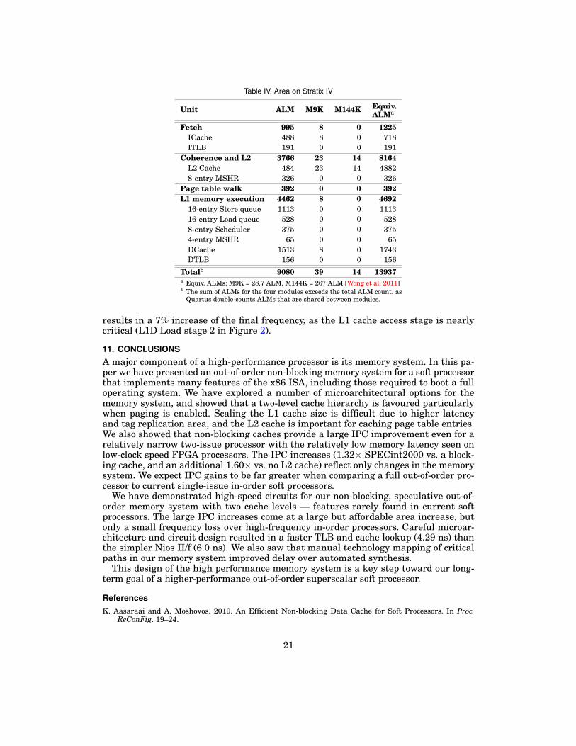
Table IV. Area on Stratix IV
Unit ALM M9K M144K Equiv.ALMa
Fetch 995 8 0 1225ICache 488 8 0 718ITLB 191 0 0 191
Coherence and L2 3766 23 14 8164L2 Cache 484 23 14 48828-entry MSHR 326 0 0 326
Page table walk 392 0 0 392L1 memory execution 4462 8 0 4692
16-entry Store queue 1113 0 0 111316-entry Load queue 528 0 0 5288-entry Scheduler 375 0 0 3754-entry MSHR 65 0 0 65DCache 1513 8 0 1743DTLB 156 0 0 156
Totalb 9080 39 14 13937a Equiv. ALMs: M9K = 28.7 ALM, M144K = 267 ALM [Wong et al. 2011]b The sum of ALMs for the four modules exceeds the total ALM count, as
Quartus double-counts ALMs that are shared between modules.
results in a 7% increase of the final frequency, as the L1 cache access stage is nearlycritical (L1D Load stage 2 in Figure 2).
11. CONCLUSIONSA major component of a high-performance processor is its memory system. In this pa-per we have presented an out-of-order non-blocking memory system for a soft processorthat implements many features of the x86 ISA, including those required to boot a fulloperating system. We have explored a number of microarchitectural options for thememory system, and showed that a two-level cache hierarchy is favoured particularlywhen paging is enabled. Scaling the L1 cache size is difficult due to higher latencyand tag replication area, and the L2 cache is important for caching page table entries.We also showed that non-blocking caches provide a large IPC improvement even for arelatively narrow two-issue processor with the relatively low memory latency seen onlow-clock speed FPGA processors. The IPC increases (1.32× SPECint2000 vs. a block-ing cache, and an additional 1.60× vs. no L2 cache) reflect only changes in the memorysystem. We expect IPC gains to be far greater when comparing a full out-of-order pro-cessor to current single-issue in-order soft processors.
We have demonstrated high-speed circuits for our non-blocking, speculative out-of-order memory system with two cache levels — features rarely found in current softprocessors. The large IPC increases come at a large but affordable area increase, butonly a small frequency loss over high-frequency in-order processors. Careful microar-chitecture and circuit design resulted in a faster TLB and cache lookup (4.29 ns) thanthe simpler Nios II/f (6.0 ns). We also saw that manual technology mapping of criticalpaths in our memory system improved delay over automated synthesis.
This design of the high performance memory system is a key step toward our long-term goal of a higher-performance out-of-order superscalar soft processor.
ReferencesK. Aasaraai and A. Moshovos. 2010. An Efficient Non-blocking Data Cache for Soft Processors. In Proc.
ReConFig. 19–24.
21
A. M. S. Abdelhadi and G. G. F. Lemieux. 2015. Modular SRAM-Based Binary Content-Addressable Memo-ries. In Proc. FCCM. 207–214.
Altera. 2015. Nios II Gen2 Processor Reference Guide.ARM. 2012. ARM Architecture Reference Manual ARMv7-A and ARMv7-R edition.J.-L. Brelet and L. Gopalakrishnan. 2002. Using Virtex-II Block RAM for High Performance Read/Write
CAMs. Xilinx Application Note XAPP260. (2002).Christopher Celio, David A. Patterson, and Krste Asanovic. 2015. The Berkeley Out-of-Order Machine
(BOOM): An Industry-Competitive, Synthesizable, Parameterized RISC-V Processor. Technical ReportUCB/EECS-2015-167. EECS Department, University of California, Berkeley. http://www.eecs.berkeley.edu/Pubs/TechRpts/2015/EECS-2015-167.html
Aeroflex Gaisler. 2015. GRLIP IP Core User’s Manual 1.4.1.M.R. Guthaus, J.S. Ringenberg, D. Ernst, T.M. Austin, T. Mudge, and R.B. Brown. 2001. MiBench:
A free, commercially representative embedded benchmark suite. In Workshop on WorkloadCharacterization(WWC-4). 3–14.
John L. Hennessy and David A. Patterson. 2003. Computer Architecture: A Quantitative Approach. MorganKaufmann, San Francisco, CA, USA.
Aamer Jaleel. 2007. Memory Characterization of Workloads Using Instrumentation-Driven Simulation.Technical Report. Intel VSSAD.
David Kroft. 1981. Lockup-free Instruction Fetch/Prefetch Cache Organization. In Proc. ISCA. Minneapolis,MN, USA, 81–87.
Belli Kuttanna. 2013. Technology Insight: Intel Silvermont Microarchitecture. IDF 2013, https://software.intel.com/sites/default/files/managed/bb/2c/02 Intel Silvermont Microarchitecture.pdf. (2013).
Damjan Lampret. OpenRISC 1200 IP Core Specification.Kevin P. Lawton. 1996. Bochs: A Portable PC Emulator for Unix/X. Linux J. 1996, 29es, Article 7 (Sept.
1996).Yunsup Lee, A. Waterman, R. Avizienis, H. Cook, Chen Sun, V. Stojanovic, and K. Asanovic. 2014. A 45nm
1.3GHz 16.7 double-precision GFLOPS/W RISC-V processor with vector accelerators. In European SolidState Circuits Conference (ESSCIRC). 199–202.
Shih-Lien L. Lu, Peter Yiannacouras, Rolf Kassa, Michael Konow, and Taeweon Suh. 2007. An FPGA-basedPentium in a Complete Desktop System. In Proc. FPGA. 53–59.
Andreas Moshovos. 1997. Dynamic Speculation and Synchronization of Data Dependencies. In Proc. ISCA.181–193.
J. Power, M.D. Hill, and D.A. Wood. 2014. Supporting x86-64 address translation for 100s of GPU lanes. InProc. HPCA. 568–578.
Graham Schelle, Jamison Collins, Ethan Schuchman, Perrry Wang, Xiang Zou, Gautham Chinya, Ralf Plate,Thorsten Mattner, Franz Olbrich, Per Hammarlund, Ronak Singhal, Jim Brayton, Sebastian Steibl, andHong Wang. 2010. Intel Nehalem Processor Core Made FPGA Synthesizable. In Proc. FPGA. 3–12.
SPEC. 2000. SPEC CPU95 Results. https://www.spec.org/cpu95/results/. (2000).Perry H. Wang, Jamison D. Collins, Christopher T. Weaver, Blliappa Kuttanna, Shahram Salamian, Gau-
tham N. Chinya, Ethan Schuchman, Oliver Schilling, Thorsten Doil, Sebastian Steibl, and Hong Wang.2009. Intel Atom Processor Core Made FPGA-synthesizable. In Proc. FPGA. 209–218.
Henry Wong, Vaughn Betz, and Jonathan Rose. 2011. Comparing FPGA vs. Custom CMOS and the Impacton Processor Microarchitecture. In Proc. FPGA. 5–14.
Henry Wong, Vaughn Betz, and Jonathan Rose. 2013. Efficient methods for out-of-order load/store executionfor high-performance soft processors. In Proc. FPT. 442–445.
Jonathan D. Woodruff. 2014. CHERI: A RISC capability machine for practical memory safety. Ph.D. Disser-tation. University of Cambridge.
Xilinx. 2014. MicroBlaze Processor Reference Guide.
22