Embed Size (px)
Citation preview

MiCOM P721 & P723
High Impedance Differential Protection
P72x/EN T/B21_
Technical Guide

Note: The technical manual for this device gives instructions for its installation, commissioning, and
operation. However, the manual cannot cover all conceivable circumstances or include detailed information on all topics. In the event of questions or specific problems, do not take any action without proper authorization. Contact the appropriate Schneider Electric technical sales office and request the necessary information.
Any agreements, commitments, and legal relationships and any obligations on the part of Schneider Electric including settlements of warranties, result solely from the applicable purchase contract, which is not affected by the contents of the technical manual.
This device MUST NOT be modified. If any modification is made without the express permission of Schneider Electric, it will invalidate the warranty, and may render the product unsafe.
The Schneider Electric logo and any alternative version thereof are trademarks and service marks of Schneider Electric.
MiCOM is a registered trademark of Schneider Electric. All trade names or trademarks mentioned herein whether registered or not, are the property of their owners.
This manual is provided for informational use only and is subject to change without notice.
© 2012, Schneider Electric. All rights reserved.

Technical Guide P72x/EN T/B21 Contents MiCOM P721/P723 Page 1/2
MiCOM P721 & P723 HIGH IMPEDANCE DIFFERENTIAL PROTECTION TECHNICAL GUIDE
CONTENTS
Safety Section Pxxx/EN SS/G11
Introduction P72x/EN IT/B21
Handling, Installation and Case Dimensions P72x/EN IN/B21
User Guide P72x/EN FT/B21
Menu Content Tables P72x/EN HI/B21
Technical Data P72x/EN TD/A11
Getting Started P72x/EN GS/B21
Communication Database P72x/EN CT/A11
Connection Diagrams P72x/EN CO/A11
Commissioning Test & Records Sheets P72x/EN RS/A11
Hardware/Software Version History and Compatibility P72x/EN VC/B21

P72x/EN T/B21 Technical Guide Contents Page 2/2 MiCOM P721/P723
BLANK PAGE

Pxxx/EN SS/G11
SAFETY SECTION


Pxxx/EN SS/G11 Safety Section Page 1/8
STANDARD SAFETY STATEMENTS AND EXTERNAL LABEL INFORMATION FOR SCHNEIDER ELECTRIC EQUIPMENT
1. INTRODUCTION 3
2. HEALTH AND SAFETY 3
3. SYMBOLS AND EXTERNAL LABELS ON THE EQUIPMENT 4
3.1 Symbols 4 3.2 Labels 4 4. INSTALLING, COMMISSIONING AND SERVICING 4
5. DECOMMISSIONING AND DISPOSAL 7
6. TECHNICAL SPECIFICATIONS FOR SAFETY 8
6.1 Protective fuse rating 8 6.2 Protective Class 8 6.3 Installation Category 8 6.4 Environment 8

Pxxx/EN SS/G11 Page 2/8 Safety Section
BLANK PAGE

Pxxx/EN SS/G11 Safety Section Page 3/8
1. INTRODUCTION This guide and the relevant equipment documentation provide full information on safe handling, commissioning and testing of this equipment. This Safety Guide also includes descriptions of equipment label markings.
Documentation for equipment ordered from Schneider Electric is despatched separately from manufactured goods and may not be received at the same time. Therefore this guide is provided to ensure that printed information which may be present on the equipment is fully understood by the recipient.
The technical data in this safety guide is typical only, see the technical data section of the relevant product publication(s) for data specific to a particular equipment.
Before carrying out any work on the equipment the user should be familiar with the contents of this Safety Guide and the ratings on the equipment’s rating label.
Reference should be made to the external connection diagram before the equipment is installed, commissioned or serviced.
Language specific, self-adhesive User Interface labels are provided in a bag for some equipment.
2. HEALTH AND SAFETY The information in the Safety Section of the equipment documentation is intended to ensure that equipment is properly installed and handled in order to maintain it in a safe condition.
It is assumed that everyone who will be associated with the equipment will be familiar with the contents of that Safety Section, or this Safety Guide.
When electrical equipment is in operation, dangerous voltages will be present in certain parts of the equipment. Failure to observe warning notices, incorrect use, or improper use may endanger personnel and equipment and also cause personal injury or physical damage.
Before working in the terminal strip area, the equipment must be isolated.
Proper and safe operation of the equipment depends on appropriate shipping and handling, proper storage, installation and commissioning, and on careful operation, maintenance and servicing. For this reason only qualified personnel may work on or operate the equipment.
Qualified personnel are individuals who:
• Are familiar with the installation, commissioning, and operation of the equipment and of the system to which it is being connected;
• Are able to safely perform switching operations in accordance with accepted safety engineering practices and are authorised to energize and de-energize equipment and to isolate, ground, and label it;
• Are trained in the care and use of safety apparatus in accordance with safety engineering practices;
• Are trained in emergency procedures (first aid).
The equipment documentation gives instructions for its installation, commissioning, and operation. However, the manual cannot cover all conceivable circumstances or include detailed information on all topics. In the event of questions or specific problems, do not take any action without proper authorization. Contact the appropriate Schneider Electric technical sales office and request the necessary information.

Pxxx/EN SS/G11 Page 4/8 Safety Section
3. SYMBOLS AND EXTERNAL LABELS ON THE EQUIPMENT For safety reasons the following symbols and external labels, which may be used on the equipment or referred to in the equipment documentation, should be understood before the equipment is installed or commissioned.
3.1 Symbols
Caution: refer to equipment documentation
Caution: risk of electric shock
Protective Conductor (*Earth) terminal
Functional/Protective Conductor (*Earth) terminal. Note: This symbol may also be used for a Protective Conductor (Earth) Terminal if that terminal is part of a terminal block or sub-assembly e.g. power supply.
*NOTE: THE TERM EARTH USED THROUGHOUT THIS GUIDE IS THE DIRECT EQUIVALENT OF THE NORTH AMERICAN TERM GROUND.
3.2 Labels
See Safety Guide (SFTY/4L M/G11-S) for equipment labelling information.
4. INSTALLING, COMMISSIONING AND SERVICING
Equipment connections
Personnel undertaking installation, commissioning or servicing work for this equipment should be aware of the correct working procedures to ensure safety.
The equipment documentation should be consulted before installing, commissioning, or servicing the equipment.
Terminals exposed during installation, commissioning and maintenance may present a hazardous voltage unless the equipment is electrically isolated.
The clamping screws of all terminal block connectors, for field wiring, using M4 screws shall be tightened to a nominal torque of 1.3 Nm.
Equipment intended for rack or panel mounting is for use on a flat surface of a Type 1 enclosure, as defined by Underwriters Laboratories (UL).
Any disassembly of the equipment may expose parts at hazardous voltage, also electronic parts may be damaged if suitable electrostatic voltage discharge (ESD) precautions are not taken.
If there is unlocked access to the rear of the equipment, care should be taken by all personnel to avoid electric shock or energy hazards.
Voltage and current connections shall be made using insulated crimp terminations to ensure that terminal block insulation requirements are maintained for safety.
Watchdog (self-monitoring) contacts are provided in numerical relays to indicate the health of the device. Schneider Electric strongly recommends that these contacts are hardwired into the substation's automation system, for alarm purposes.

Pxxx/EN SS/G11 Safety Section Page 5/8
To ensure that wires are correctly terminated the correct crimp terminal and tool for the wire size should be used.
The equipment must be connected in accordance with the appropriate connection diagram.
Protection Class I Equipment
- Before energizing the equipment it must be earthed using the protective conductor terminal, if provided, or the appropriate termination of the supply plug in the case of plug connected equipment.
- The protective conductor (earth) connection must not be removed since the protection against electric shock provided by the equipment would be lost.
- When the protective (earth) conductor terminal (PCT) is also used to terminate cable screens, etc., it is essential that the integrity of the protective (earth) conductor is checked after the addition or removal of such functional earth connections. For M4 stud PCTs the integrity of the protective (earth) connections should be ensured by use of a locknut or similar.
The recommended minimum protective conductor (earth) wire size is 2.5 mm² (3.3 mm² for North America) unless otherwise stated in the technical data section of the equipment documentation, or otherwise required by local or country wiring regulations.
The protective conductor (earth) connection must be low-inductance and as short as possible.
All connections to the equipment must have a defined potential. Connections that are pre-wired, but not used, should preferably be grounded when binary inputs and output relays are isolated. When binary inputs and output relays are connected to common potential, the pre-wired but unused connections should be connected to the common potential of the grouped connections.
Before energizing the equipment, the following should be checked:
- Voltage rating/polarity (rating label/equipment documentation),
- CT circuit rating (rating label) and integrity of connections,
- Protective fuse rating,
- Integrity of the protective conductor (earth) connection (where applicable),
- Voltage and current rating of external wiring, applicable to the application.
Accidental touching of exposed terminals
If working in an area of restricted space, such as a cubicle, where there is a risk of electric shock due to accidental touching of terminals which do not comply with IP20 rating, then a suitable protective barrier should be provided.
Equipment use
If the equipment is used in a manner not specified by the manufacturer, the protection provided by the equipment may be impaired.
Removal of the equipment front panel/cover
Removal of the equipment front panel/cover may expose hazardous live parts, which must not be touched until the electrical power is removed.

Pxxx/EN SS/G11 Page 6/8 Safety Section
UL and CSA/CUL Listed or Recognized equipment
To maintain UL and CSA/CUL Listing/Recognized status for North America the equipment should be installed using UL or CSA Listed or Recognized parts for the following items: connection cables, protective fuses/fuseholders or circuit breakers, insulation crimp terminals and replacement internal battery, as specified in the equipment documentation.
For external protective fuses a UL or CSA Listed fuse shall be used. The Listed type shall be a Class J time delay fuse, with a maximum current rating of 15 A and a minimum d.c. rating of 250 Vd.c., for example type AJT15.
Where UL or CSA Listing of the equipment is not required, a high rupture capacity (HRC) fuse type with a maximum current rating of 16 Amps and a minimum d.c. rating of 250 Vd.c. may be used, for example Red Spot type NIT or TIA.
Equipment operating conditions
The equipment should be operated within the specified electrical and environmental limits.
Current transformer circuits
Do not open the secondary circuit of a live CT since the high voltage produced may be lethal to personnel and could damage insulation. Generally, for safety, the secondary of the line CT must be shorted before opening any connections to it.
For most equipment with ring-terminal connections, the threaded terminal block for current transformer termination has automatic CT shorting on removal of the module. Therefore external shorting of the CTs may not be required, the equipment documentation should be checked to see if this applies.
For equipment with pin-terminal connections, the threaded terminal block for current transformer termination does NOT have automatic CT shorting on removal of the module.
External resistors, including voltage dependent resistors (VDRs)
Where external resistors, including voltage dependent resistors (VDRs), are fitted to the equipment, these may present a risk of electric shock or burns, if touched.
Battery replacement
Where internal batteries are fitted they should be replaced with the recommended type and be installed with the correct polarity to avoid possible damage to the equipment, buildings and persons.
Insulation and dielectric strength testing
Insulation testing may leave capacitors charged up to a hazardous voltage. At the end of each part of the test, the voltage should be gradually reduced to zero, to discharge capacitors, before the test leads are disconnected.
Insertion of modules and pcb cards
Modules and PCB cards must not be inserted into or withdrawn from the equipment whilst it is energized, since this may result in damage.
Insertion and withdrawal of extender cards
Extender cards are available for some equipment. If an extender card is used, this should not be inserted or withdrawn from the equipment whilst it is energized. This is to avoid possible shock or damage hazards. Hazardous live voltages may be accessible on the extender card.

Pxxx/EN SS/G11 Safety Section Page 7/8
External test blocks and test plugs
Great care should be taken when using external test blocks and test plugs such as the MMLG, MMLB and MiCOM P990 types, hazardous voltages may be accessible when using these. *CT shorting links must be in place before the insertion or removal of MMLB test plugs, to avoid potentially lethal voltages.
*Note: When a MiCOM P992 Test Plug is inserted into the MiCOM P991 Test Block, the secondaries of the line CTs are automatically shorted, making them safe.
Fiber optic communication
Where fiber optic communication devices are fitted, these should not be viewed directly. Optical power meters should be used to determine the operation or signal level of the device.
Cleaning
The equipment may be cleaned using a lint free cloth dampened with clean water, when no connections are energized. Contact fingers of test plugs are normally protected by petroleum jelly, which should not be removed.
5. DECOMMISSIONING AND DISPOSAL
De-commissioning The supply input (auxiliary) for the equipment may include capacitors across the supply or to earth. To avoid electric shock or energy hazards, after completely isolating the supplies to the equipment (both poles of any dc supply), the capacitors should be safely discharged via the external terminals prior to de-commissioning.
Disposal
It is recommended that incineration and disposal to water courses is avoided. The equipment should be disposed of in a safe manner. Any equipment containing batteries should have them removed before disposal, taking precautions to avoid short circuits. Particular regulations within the country of operation, may apply to the disposal of the equipment.

Pxxx/EN SS/G11 Page 8/8 Safety Section
6. TECHNICAL SPECIFICATIONS FOR SAFETY Unless otherwise stated in the equipment technical manual, the following data is applicable.
6.1 Protective fuse rating The recommended maximum rating of the external protective fuse for equipments is 16A, high rupture capacity (HRC) Red Spot type NIT, or TIA, or equivalent. Unless otherwise stated in equipment technical manual, the following data is applicable. The protective fuse should be located as close to the unit as possible.
CAUTION - CTs must NOT be fused since open circuiting them may produce lethal hazardous voltages.
6.2 Protective Class
IEC 60255-27: 2005
EN 60255-27: 2006
Class I (unless otherwise specified in the equipment documentation). This equipment requires a protective conductor (earth) connection to ensure user safety.
6.3 Installation Category
IEC 60255-27: 2005
EN 60255-27: 2006
Installation Category III (Overvoltage Category III):
Distribution level, fixed installation.
Equipment in this category is qualification tested at 5 kV peak, 1.2/50 µs, 500 Ω, 0.5 J, between all supply circuits and earth and also between independent circuits.
6.4 Environment
The equipment is intended for indoor installation and use only. If it is required for use in an outdoor environment then it must be mounted in a specific cabinet or housing which will enable it to meet the requirements of IEC 60529 with the classification of degree of protection IP54 (dust and splashing water protected).
Pollution Degree - Pollution Degree 2 Compliance is demonstrated by reference Altitude - Operation up to 2000m to safety standards.
IEC 60255-27:2005
EN 60255-27: 2006

Introduction P72x/EN IT/B21 MiCOM P721/P723
INTRODUCTION

Introduction P72x/EN IT/B21 MiCOM P721/P723 Page 1/10
CONTENTS
1. INTRODUCTION 3
2. HOW TO USE THIS MANUAL 4
3. INTRODUCTION TO THE MiCOM RANGE 5
4. INTRODUCTION TO THE MiCOM P721 & P723 PROTECTIONS 6
5. MAIN FUNCTIONS 7
5.1 Main functions 7 5.2 General functions 7 5.3 Ordering options 9

P72x/EN IT/B21 Introduction Page 2/10 MiCOM P721/P723
BLANK PAGE

Introduction P72x/EN IT/B21 MiCOM P721/P723 Page 3/10
1. INTRODUCTION The differential protections of the MiCOM P72x range are Schneider Electric numerical high impedance differential protection. MiCOM P721 and P723 have been designed to provide differential protection and a high impedance differential protection
The differential protection consists to measure the summation of n Current Transformers (CTs) secondary currents. Without internal fault, this sum is null. If an internal fault occurs, the protection measures the leak current. If an external fault occurs (with non-saturated CT), the Kirchhoff's law is conserved and no current is measured.
The high impedance differential protection main application is a CT saturation in a busbar (when a serious and external fault occurs).

P72x/EN IT/B21 Introduction Page 4/10 MiCOM P721/P723
2. HOW TO USE THIS MANUAL This manual provides a description of MiCOM P721 and P723 functions and settings. The goal of this manual is to allow the user to become familiar with the application, installation, setting and commissioning of these relays.
This manual has the following format:
P72x/EN IT Introduction
The introduction presents the documentation structure and a brief presentation of the relay, including functions.
P72x/EN IN Handling, installation and case dimensions
This section provides logistics general instructions for handling, installing and stocking..
P72x/EN FT User Guide
This section provides relay settings with a brief explanation of each setting and detailed description. It also provides recording and measurements functions including the configuration of the event and disturbance recorder and measurement functions.
P72x/EN HI Menu content tables
This section shows the menu structure of the relays, with a complete list of all of the menu settings.
P72x/EN TD Technical data and curve characteristics
This section provides technical data including setting ranges, accuracy limits, recommended operating conditions, ratings and performance data. Compliance with norms and international standards is quoted where appropriate.
P72x/EN CT Communication database
This section provides an overview regarding the communication interfaces of the relay. Detailed protocol mappings, semantics, profiles and interoperability tables are not provided within this manual. Separate documents are available per protocol, available for download from our website.
P72x/EN CO Connection diagrams
This section provides the mechanical and electrical description. External wiring connections to the relay are indicated.
P72x/EN RS Commissioning test and records sheets
This section contains checks on the calibration and functionality of the relay.
P72x/EN VC Hardware/Software version history and compatibility
History of all hardware and software releases for the product.

Introduction P72x/EN IT/B21 MiCOM P721/P723 Page 5/10
3. INTRODUCTION TO THE MiCOM RANGE MiCOM is a comprehensive solution capable of meeting all electricity supply requirements. It comprises of a range of components, systems and services from Schneider Electric. Flexibility is central to the MiCOM concept.
MiCOM provides the ability to define an application solution and, through extensive communication capabilities, to integrate this solution with your power supply control system.
The components within MiCOM are:
• P range protection relays
• C range control products
• M range measurement products for accurate metering and monitoring
• S range versatile PC support and substation control packages
MiCOM products include extensive facilities for recording information on the state and behaviour of a power system, using disturbance and fault records.
They can also provide measurements of the power system at regular intervals to a control centre enabling remote monitoring and control to take place.
For up-to-date information on any MiCOM product, refer to the technical publications, which can be obtained from: Schneider Electric or your local sales office; alternatively visit our web site.
www.schneider-electric.com

P72x/EN IT/B21 Introduction Page 6/10 MiCOM P721/P723
4. INTRODUCTION TO THE MiCOM P721 & P723 PROTECTIONS The range of MiCOM protection relays is built on the success of the MIDOS, K and MODN ranges by incorporating the last changes in digital technology. Relays from the MiCOM P72x range are fully compatible and use the same modular box concept.
MiCOM P721 and P723 high impedance differential protections provide differential protection and high impedance differential protection (with P79x high impedance accessory) for machines, power transformers and busbar installations as well as for other applications where differential protection is required.
The P721 relay provides simple restricted earth current fault protection. Furthermore, P723 relay is used for 3-phases fault protection.
In addition to its protective functions, each relay offers control and recording features. They can be fully integrated to a control system so protection, control, data acquisition and recording of faults, events and disturbances can be made available.
The relays are equipped on the front panel with a liquid crystal display (LCD) with 2 x 16 back-lit alphanumerical characters, a tactile 7 button keypad (to access all settings, clear alarms and read measurements) and 8 LEDs that indicate the status of MiCOM P721 and P723 protections.
In addition, the use of the RS485 communication port makes it possible to read, reinitialise and change the settings of the relays, if required, from a local or remote PC computer loaded with MiCOM S1 software.
Its flexibility of use, reduced maintenance requirements and ease of integration allow the MiCOM P72x range to provide an adaptable solution for the problems of the protection of electric networks.

Introduction P72x/EN IT/B21 MiCOM P721/P723 Page 7/10
5. MAIN FUNCTIONS 5.1 Main functions
The following table shows the functions available for the different models of the MiCOM P72x range of relays.
ANSI CODES FEATURES P721 P723
87 Phase segregated high impedance current differential protection •
95 Phase bus-wire supervision • 87N Restricted earth fault protection • • 95N Earth bus-wire supervision • •
87CZ Check zone input • 50BF Breaker failure detection • •
5.2 General functions
The following table shows the general features available.
GENERAL FEATURES P721 P723
Number of digital inputs 2 5
Total number of outputs relays
4 8
Events recording 250 250
Fault recording 25 25
Disturbance recording 5 5
Instantaneous records 5 5
Setting group 2 2
Auxiliary timers 2 4
Communication IEC60870-5-103, DNP 3.0 & Modbus RTU (rear and front port) • •
Settings software MiCOM S1 • •
Logic equation AND, OR and NOT gates (8 equations) • •
Measurements Neutral supervision / differential currents (INdiff) • •
Phase supervision / differential currents (IAdiff, IBdiff and ICdiff) •
Maximum differential currents (ImaxAdiff, ImaxBdiff, and ImaxCdiff) •
Maximum differential neutral currents (ImaxNdiff • •

P72x/EN IT/B21 Introduction Page 8/10 MiCOM P721/P723
Application overview
FIGURE 1: FUNCTIONAL DIAGRAM

Introduction P72x/EN IT/B21 MiCOM P721/P723 Page 9/10
5.3 Ordering options
Information Required with Order
Relay Type (differential protection) P72 0 0 0
Variant Simple phase high impedance differential protection Simple phase or three phase high impedance protection with binary I/O extension
1
3
Auxiliary and digital input voltage
Auxiliary voltage digital input voltage
48-250 Vdc / 48-240 Vac48-250 Vdc / 48-240 Vac48-250 Vdc / 48-240 Vac48-250 Vdc / 48-240 Vac24-250Vdc / 48-240Vac
105-145 Vdc (1) 48-250 Vdc (ENA UK) 110 Vdc –30% / +20% (1) 220 Vdc –30% / +20% (1) 24-250 Vdc / 24 / 240 Vdc
H T V W Z
Rear port communication interface
Modbus K-Bus/Courier IEC 60870-5-103 DNP 3.0
1 2 3 4
Default HMI language
French English / American Spanish German Italian Portuguese
0 1 2 3 4 7
Platform
phase 2 with standard software 2
Software
Unless specified the latest version will be delivered
Mounting option
None (default) (2) Pre-fixed HMI (no withdrawability) Sealed cover (2) Pre-fixed HMI + Sealed cover
0123
(1) : special application (2) : : not available

P72x/EN IT/B21 Introduction Page 10/10 MiCOM P721/P723
BLANK PAGE

Handling, Installation and Case Dimensions P72x/EN IN/B21 MiCOM P721/P723
HANDLING, INSTALLATION AND CASE DIMENSIONS

Handling, Installation and Case Dimensions P72x/EN IN/B21 MiCOM P721/P723 Page 1/10
CONTENTS
1. GENERAL CONSIDERATIONS 3
1.1 Receipt of relays 3 1.2 Electrostatic discharge (ESD) 3
2. HANDLING OF ELECTRONIC EQUIPMENT 4
3. RELAY MOUNTING 5
4. UNPACKING 6
5. STORAGE 7
6. DIMENSIONS 8
6.1 Connection of power terminals, and Signals terminals 8 6.2 Communication port RS485 9 6.3 Earthing 9
7. CASE DIMENSIONS 10

P72x/EN IN/B21 Handling, Installation and Case Dimensions Page 2/10 MiCOM P721/P723
BLANK PAGE
Handling, Installation and Case Dimensions P72x/EN IN/B21 MiCOM P721/P723 Page 3/10
1. GENERAL CONSIDERATIONS
BEFORE CARRYING OUT ANY WORK ON THE EQUIPMENT, THE USER SHOULD BE FAMILIAR WITH THE CONTENTS OF THE SAFETY GUIDE SFTY/4LM/G11-S OR LATER ISSUE, OR THE SAFETY AND TECHNICAL DATA SECTIONS OF THE TECHNICAL MANUAL AND ALSO THE RATINGS ON THE EQUIPMENT RATING LABEL.
1.1 Receipt of relays
Protective relays, although generally of robust construction, require careful treatment prior to installation on site. Upon receipt, relays should be examined immediately to ensure no damage has been sustained in transit. If damage has been sustained during transit a claim should be made to the transport contractor and Schneider Electric should be promptly notified.
Relays that are supplied unmounted and not intended to be installed immediately should be returned with their protective polythene bags.
1.2 Electrostatic discharge (ESD)
The relays use components that are sensitive to electrostatic discharges.
The electronic circuits are well protected by the metal case and the internal module should not be withdrawn unnecessarily. When handling the module outside its case, care should be taken to avoid contact with components and electrical connections. If removed from the case for storage, the module should be placed in an electrically conducting antistatic bag.
There are no setting adjustments within the module and it is advised that it is not unnecessarily disassembled. Although the printed circuit boards are plugged together, the connectors are a manufacturing aid and not intended for frequent dismantling; in fact considerable effort may be required to separate them. Touching the printed circuit board should be avoided, since complementary metal oxide semiconductors (CMOS) are used, which can be damaged by static electricity discharged from the body.

P72x/EN IN/B21 Handling, Installation and Case Dimensions Page 4/10 MiCOM P721/P723
2. HANDLING OF ELECTRONIC EQUIPMENT A person’s normal movements can easily generate electrostatic potentials of several thousand volts. Discharge of these voltages into semiconductor devices when handling electronic circuits can cause serious damage, which often may not be immediately apparent but the reliability of the circuit will have been reduced.
The electronic circuits are completely safe from electrostatic discharge when housed in the case. Do not expose them to risk of damage by withdrawing modules unnecessarily.
Each module incorporates the highest practicable protection for its semiconductor devices. However, if it becomes necessary to withdraw a module, the following precautions should be taken to preserve the high reliability and long life for which the equipment has been designed and manufactured.
1. Before removing a module, ensure that you are at the same electrostatic potential as the equipment by touching the case.
2. Handle the module by its frontplate, frame or edges of the printed circuit board. Avoid touching the electronic components, printed circuit track or connectors.
3. Do not pass the module to another person without first ensuring you are both at the same electrostatic potential. Shaking hands achieves equipotential.
4. Place the module on an antistatic surface, or on a conducting surface which is at the same potential as yourself.
5. Store or transport the module in a conductive bag.
If you are making measurements on the internal electronic circuitry of an equipment in service, it is preferable that you are earthed to the case with a conductive wrist strap. Wrist straps should have a resistance to ground between 500kΩ – 10MΩ.
If a wrist strap is not available you should maintain regular contact with the case to prevent a build-up of static. Instrumentation which may be used for making measurements should be earthed to the case whenever possible.
More information on safe working procedures for all electronic equipment can be found in BS5783 and IEC 147-OF. It is strongly recommended that detailed investigations on electronic circuitry or modification work should be carried out in a special handling area such as described in the above-mentioned BS and IEC documents.

Handling, Installation and Case Dimensions P72x/EN IN/B21 MiCOM P721/P723 Page 5/10
3. RELAY MOUNTING Relays are dispatched either individually or as part of a panel/rack assembly.
If an MMLG test block is to be included it should be positioned at the right-hand side of the assembly (viewed from the front). Modules should remain protected by their metal case during assembly into a panel or rack.
For individually mounted relays an outline diagram is supplied in section 6 of this chapter showing the panel cut-outs and hole centres.

P72x/EN IN/B21 Handling, Installation and Case Dimensions Page 6/10 MiCOM P721/P723
4. UNPACKING Care must be taken when unpacking and installing the relays so that none of the parts is damaged or the settings altered. Relays must only be handled by skilled personnel. The installation should be clean, dry and reasonably free from dust and excessive vibration. The site should be well lit to facilitate inspection. Relays that have been removed from their cases should not be left in situations where they are exposed to dust or damp. This particularly applies to installations which are being carried out at the same time as construction work.

Handling, Installation and Case Dimensions P72x/EN IN/B21 MiCOM P721/P723 Page 7/10
5. STORAGE If relays are not to be installed immediately upon receipt they should be stored in a place free from dust and moisture in their original cartons. Where de-humidifier bags have been included in the packing they should be retained. The action of the de-humidifier crystals will be impaired if the bag has been exposed to ambient conditions and may be restored by gently heating the bag for about an hour, prior to replacing it in the carton.
Dust which collects on a carton may, on subsequent unpacking, find its way into the relay; in damp conditions the carton and packing may become impregnated with moisture and the de-humifier will lose its efficiency.
Storage temperature: –25°C to +70°C.

P72x/EN IN/B21 Handling, Installation and Case Dimensions Page 8/10 MiCOM P721/P723
6. DIMENSIONS 6.1 Connection of power terminals, and Signals terminals
The individual equipment are delivered with sufficient M4 screws to connect the relay via annular terminals, with a maximum recommended of two annular terminals per contact.
If necessary, Schneider Electric can provide annular terminals to crimp. 5 references exist according to the section of the wire (see below). Each reference corresponds to a sachet of 100 terminals.
To insure the insulation of the terminals and to respect the security and safety instructions, an isolated sleeve can be used.
We recommend the following cable cross-sections:
− Auxiliary sources Vaux: 1.5 mm²
− Communication Port see paragraph 6.2
− Other circuits 1.0 mm²
Because of the limitations of the annular terminals, the maximum wire cross-section which can be used for the connector blocks (for current inputs and signals) is of 6mm² by using non -insulated annular terminals. When only pre- insulated terminals can be used, the maximum wire cross-section is reduced to 2, 63 mm² per annular terminal. If a more significant wire cross-section is necessary, two wires can be put in parallel, each one finished by a separate annular terminal.
All the terminal blocks used for connections, except of the port RS485, must be able to withstand a nominal voltage of minimum 300V peak value.
We recommend to protect the auxiliary source connection by using a fuse of type NIT or TIA with a breaking capacity of 16A. For security reasons, do never install fuses in current transformers circuits. The other circuits must be protected by fuses.

Handling, Installation and Case Dimensions P72x/EN IN/B21 MiCOM P721/P723 Page 9/10 6.2 Communication port RS485
Connections to RS485 is made using annular terminals. It is recommended that a two core screened cable, is used with a maximum total length of 1000 m or a200nF total cable capacitance.
Typical specification:
− Each core: 16/0.2 mm copper conductor, PVC insulated.
− Nominal conductor area: 0.5 mm² per core
− Screen: Overall braid, PVC sheathed
− Linear capacitance between conductor and earth: 100pF/m
6.3 Earthing
Each equipment must be connected to a local earth terminal by the intermediary of a M4 earth terminals. We recommend a wire of minimal section of 2.5 mm², with annular terminals on the side of the equipment. Because of the limitations of the annular terminals, the possible maximum section is of 6mm² by wire. If a larger section is necessary, one can use cables connected in parallel, each one ending with an annular terminal separated on the side of the equipment. One can also use a metal bar.
NOTE: To prevent any electrolytic risk between copper conductor or brass conductor and the back plate of the equipment, it is necessary to take precautions to isolate them one from the other. This can be done in several ways, for example by inserting between the conductor and the case a plated nickel or insulated ring washer or by using a tin terminals.

P72x/EN IN/B21 Handling, Installation and Case Dimensions Page 10/10 MiCOM P721/P723
7. CASE DIMENSIONS MiCOM P721 and P723 relays are available in a 4U metal case for panel or flush mounting.
Weight: 1.7 to 2.1 Kg
External size: Height case 152 mm front panel 177 mm Width case 97 mm front panel 103 mm Depth case 226 mm front panel + case 252 mm
P0078ENb
MiCOM P721 AND P723 RELAYS CASE DIMENSIONS
NOTE: The chassis is normally secured in the case by four screws (Self tap
screws 6x1.4), to ensure good seating. The fixing screws should be fitted in normal service (do not add washers). Do not discard these screws.

User Guide P72x/EN FT/B21 MiCOM P721/P723
USER GUIDE


User Guide P72x/EN FT/B21 MiCOM P721/P723 Page 1/38
CONTENTS
1. PRESENTATION OF MiCOM P721 AND P723 PROTECTIONS 3 1.1 USER INTERFACE 4 1.1.1 Relay Overview 4 1.1.2 Front panel description 5 1.1.3 LCD display and keypad description 6 1.1.4 LEDs 7 1.1.5 Description of the two areas under the top and bottom flaps 8 1.1.6 The USB/RS232 cable (to power and set the relay) 8 1.2 Menu structure 9 1.3 Password 9 1.3.1 Password protection 9 1.3.2 Password entry 9 1.3.3 Changing the password 10 1.3.4 Change of setting invalidation 10 1.4 Displays of Alarm & Warning Messages 10 1.4.1 Electrical Network Alarms 10
2. MENUS 13 2.1 Default display 13 2.2 Menu contents description 13 2.3 OP PARAMETERS Menu 14 2.4 CONFIGURATION menu 15 2.4.1 Submenu CONFIGURATION 15 2.4.2 Submenus LED 5 to 8 16 2.4.3 Submenu GROUP SELECT 18 2.4.4 Submenu ALARMS 18 2.4.5 Submenu INPUTS 19 2.4.6 Submenu OUTPUT RELAYS 19 2.5 MEASUREMENTS Menu 20 2.5.1 If Earth protection is selected 20 2.5.2 If Phase protection is selected (P723 only) 20 2.6 COMMUNICATION Menu 21 2.7 PROTECTION Menu 22 2.7.1 Earth protection configuration 22 2.7.2 Phase protection configuration 24 2.8 AUTOMAT. CTRL Menu 25 2.8.1 Submenu Trip Commands 25 2.8.2 Submenu Latch of trip output relay by Function 26 2.8.3 Submenu Blocking Logic 1 / 2 27 2.8.4 Outputs Relays submenu 27

P72x/EN FT/B21 User Guide Page 2/38 MiCOM P721/P723 2.8.5 Latch of the auxiliary output relays (RL2 to RL8) 29 2.8.6 Inputs submenu 29 2.8.7 CIRCUIT BREAKER FAILURE submenu 31 2.8.8 Submenu Logic Equations 31 2.9 RECORDS Menu 34 2.9.1 Fault Record submenu 34 2.9.2 INSTANTANEOUS RECORDS submenu 35 2.9.3 DISTURBANCE RECORD submenu 35
3. WIRING 36 3.1 Auxiliary supply 36 3.2 Current measurement inputs 36 3.3 Logic inputs 36 3.4 Output relays 36 3.5 Communication 37 3.5.1 RS485 rear communication port 37 3.5.2 RS232 front communication port 37

User Guide P72x/EN FT/B21 MiCOM P721/P723 Page 3/38
1. PRESENTATION OF MiCOM P721 AND P723 PROTECTIONS MiCOM P721 and P723 are fully numerical relays designed to perform electrical protection and control functions.
The following section describes the MiCOM P72x range and the main differences between the different models.
MiCOM relays are powered either from a DC (2 voltage ranges) or an AC auxiliary power supply.
Using the front panel, the user can easily navigate through the menu and access data, change settings, read measurements, etc.
Eight LEDs situated in the front panel help the user to quickly know the status of the relay and the presence of alarms. Alarms that have been detected are stored and can be displayed on the back-lit LCD.
Any short time voltage interruption (<50ms) is filtered and regulated through the auxiliary power supply.
Regarding current inputs, MiCOM P721 has one earth current input available for 1A and 5A rated CTs.
MiCOM P723 has 3 phase and 1 earth current inputs available for 1 and 5 Amps rated CTs. On each one of these relays, it is possible to combine 1 and 5 Amp current inputs together (i-e a mix between 1A for earth fault and 5A for phase connections).
MiCOM P721 and P723 relays continuously measure phase and earth currents and take into account the true RMS current value up to 10th harmonic (at 50 Hz).
Output relays are freely configurable and can be activated by any of the control or protection functions available in the relay. Logic inputs can also be assigned to various control functions.
On their rear terminals MiCOM P721 and P723 have a standard RS485 port available. When ordering, the user can choose between the following communication protocols: ModBus RTU, IEC 60870-5-103 or DNP3.0.
Using RS485 communication channel, all stored information (measurements, alarms, and parameters) can be read and settings can be modified when the chosen protocol allows it.
Reading and modification of this data can be carried out on site with a standard PC loaded with Schneider Electric setting software.
Thanks to its RS485 based communication, MiCOM P721 and P723 relays can be connected directly to a digital control system. All the available data can then be gathered by a substation control system and be processed either locally or remotely.

P72x/EN FT/B21 User Guide Page 4/38 MiCOM P721/P723 1.1 USER INTERFACE
1.1.1 Relay Overview
The next figures show the P721 and P723 protections.
The table shows the case size.
Height Depth Width
4U (177mm) 226mm 20 TE
The hinged covers at the top and bottom of the relay are shown closed. Extra physical protection for the front panel can be provided by an optional transparent front cover; this allows read only access to the relays settings and data but does not affect the relays IP rating. When full access to the relay keypad is required to edit the settings, the transparent cover can be unclipped and removed when the top and bottom hinged covers are open.

User Guide P72x/EN FT/B21 MiCOM P721/P723 Page 5/38 1.1.2 Front panel description
MiCOM P721 and P723 relay front panel allows the user to easily enter relay settings, display measured values and alarms and to clearly display the status of the relay.
Front comms port
Fixed function
LED
User programmablefunction LEDs
Cover (not used)
Top cover
Keypad
P3602ENg
Front comms port
Fixed function
LED
User programmablefunction LEDs
Cover (not used)
Top cover
Keypad
P3602ENg
FIGURE 1: MiCOM P721 AND P723 FRONT PANEL DESCRIPTION
The front panel of the relay has three separate sections:
1. The LCD display and the keypad,
2. The LEDs
3. The two zones under the upper and lower flaps.
P72x/EN FT/B21 User Guide Page 6/38 MiCOM P721/P723 1.1.3 LCD display and keypad description
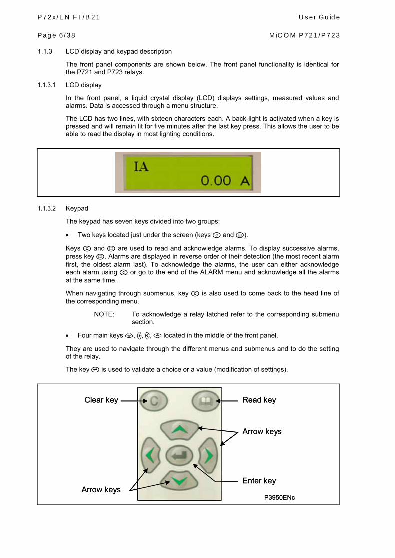
The front panel components are shown below. The front panel functionality is identical for the P721 and P723 relays.
1.1.3.1 LCD display
In the front panel, a liquid crystal display (LCD) displays settings, measured values and alarms. Data is accessed through a menu structure.
The LCD has two lines, with sixteen characters each. A back-light is activated when a key is pressed and will remain lit for five minutes after the last key press. This allows the user to be able to read the display in most lighting conditions.
1.1.3.2 Keypad
The keypad has seven keys divided into two groups:
• Two keys located just under the screen (keys and ).
Keys and are used to read and acknowledge alarms. To display successive alarms, press key . Alarms are displayed in reverse order of their detection (the most recent alarm first, the oldest alarm last). To acknowledge the alarms, the user can either acknowledge each alarm using or go to the end of the ALARM menu and acknowledge all the alarms at the same time.
When navigating through submenus, key is also used to come back to the head line of the corresponding menu.
NOTE: To acknowledge a relay latched refer to the corresponding submenu section.
• Four main keys , , , located in the middle of the front panel.
They are used to navigate through the different menus and submenus and to do the setting of the relay.
The key is used to validate a choice or a value (modification of settings).
Read key
Arrow keys
Enter keyArrow keys
Clear key
P3950ENc
Read key
Arrow keys
Enter keyArrow keys
Clear key
P3950ENc

User Guide P72x/EN FT/B21 MiCOM P721/P723 Page 7/38 1.1.4 LEDs
The LED labels on the front panel are by default written in English, however the user has self-adhesive labels available with MiCOM relays on which it is possible to write using a ball point pen.
The top four LEDs indicate the status of the relay (Trip condition, alarm LED, equipment failure, auxiliary supply).
The four lower LEDs are freely programmable by the user and can be assigned to display a threshold crossing for example (available for all models) or to show the status of the logic inputs.The description of each one of these eight LEDs located in the left side of the front view is given hereafter (numbered from the top to bottom from 1 to 8):
LED 8
LED 1
P3951ENa
LED 1 Colour: RED Label: Trip
LED 1 indicates that the relay has issued a trip order to the cut-off element. This LED recopies the trip order issued to the Trip logic output. Its normal state is unlit. As soon as a triggering order is issued, the LED lights up. It is cleared when the associated alarm is acknowledged either through the front panel, or by a remote command, a digital input, or by a new fault (CONFIGURATION/Alarms menu).
LED 2 Colour: ORANGE Label: ALARM
LED 2 indicates that the relay has detected an alarm. This alarm can either be a threshold crossing (instantaneous), or a trip order (time delayed). As soon as an alarm is detected, the LED starts blinking. After all the alarms have been read, the LED lights up continuously.
After acknowledgement of all the alarms, the LED is extinguished.
NOTE: It is possible to configure the instantaneous alarms to be self reset or not by choosing Yes or No in the CONFIGURATION/Alarms Menu.
The alarm LED can be reset either through the front panel, or by remote command, by a digital input, or by a new fault (CONFIGURATION/Alarms menu).
LED 3 Colour: ORANGE Label: Warning
LED 3 indicates internal alarms of the relay. When the relay detects a « non critical » internal alarm (typically a communication failure), the LED starts blinking continuously. When the relay detects a fault that is considered as « critical », the LED lights up continuously. Only the disappearance of the cause of the fault can clear this LED (repair of the module, clearance of the Fault).
LED 4 Colour: GREEN Label: Healthy
LED 4 indicates that the relay is powered by an auxiliary source at the nominal range.
LED 5 to 8 Colour: RED Label: Aux.1 to 4.
P72x/EN FT/B21 User Guide Page 8/38 MiCOM P721/P723
These LEDs are user programmable and can be set to display information about instantaneous and time-delayed thresholds as well as the status of the logic inputs. Under the CONFIGURATION/LED menu of the relay, the user can select the information he wishes to associate with each LED. He can affect more than one function to one LED. The LED will then light up when at least one of the associated information is valid (OR gate). The LED is cleared when all the associated alarms are acknowledged.
1.1.5 Description of the two areas under the top and bottom flaps
1.1.5.1 Relay Identification
Under the upper flap, a label identifies the relay according to its model number (order number) and its serial number. This information defines the product in a way that is unique. In all your requests, please make reference to these two numbers.
Under the model and serial number, you will find information about the level of voltage of the auxiliary supply and the nominal earth current value.
1.1.5.2 Lower flap
Under the lower flap, a RS232 port is available in all MiCOM relays. It can be used either to download a new version of the application software version into the relay flash memory or to download/retrieve settings plugging a laptop loaded with MiCOM S1 setting software.
To withdraw more easily the active part of the MiCOM relay (i-e the chassis) from its case, open and remove the two flaps, then with a 3mm screwdriver, turn the extractor located under the upper flap, and pull it out of its case pulling the flaps towards you.
1.1.6 The USB/RS232 cable (to power and set the relay)
The USB/RS232 cable is able to perform the following functions:
1. It is able to power the relay from its front port. This allows the user to view or modify data on the relay even when the auxiliary power supply of the relay has failed or when the relay is not connected to any power supply. The USB port of the PC supplies the power necessary to energize the relay. This lasts as long as the battery of the PC can last.
2. It provides an USB / RS 232 interface between the MiCOM relay and the PC. This allows the user to be able to change the setting of the relay using a PC with its USB port.
It eases the use of the relay allowing the retrieval of records and disturbance files for example when the auxiliary supply has failed or is not available.
The associated driver (supplied with the relay) needs to be installed in the PC. For more information, refer to MiCOM E2 User Guide.

User Guide P72x/EN FT/B21 MiCOM P721/P723 Page 9/38 1.2 Menu structure
The relay’s menu is arranged in a tabular structure. Each setting in the menu is referred to as a cell, and each cell in the menu may be accessed by reference to a row and column address. The settings are arranged so that each column contains related settings, for example all of the disturbance recorder settings are contained within the same column. As shown in the figure, the top row of each column contains the heading that describes the settings contained within that column. Movement between the columns of the menu can only be made at the column heading level. A complete list of all of the menu settings is given in the Menu Content tables (P72x/EH HI section).
Column
P0106ENb
data
settings
Column header
OP
paramConfig. Measur. Comm. Autom. Ctrl RecordsProtections
MENU STRUCTURE
1.3 Password
1.3.1 Password protection
A password is required for relay settings, especially when changing the various thresholds, time delays, communication parameters, allocation of inputs and outputs relays.
The password consists of four capital characters. When leaving factory, the password is set to AAAA. The user can define his own combination of four characters.
Should the password be lost or forgotten, the modification of the stored parameters is blocked. It is then necessary to contact the manufacturer or his representative and a stand-by password specific to the relay may be obtained.
The programming mode is indicated with the letter "P" on the right hand side of the display on each menu heading. The letter "P" remains present as long as the password is active (5 minutes if there is no action on the keypad).
1.3.2 Password entry
The input of the password is requested as soon as a modification of a parameter is made for any one of the six/eight menus and the submenus. The user enters each one of the 4 characters and then validates the entire password with .
After 5 seconds, the display returns to the point of the preceding menu.
If no key is pressed inside of 5 minutes, the password is deactivated. A new password request is associated with any subsequent parameter modification.
P72x/EN FT/B21 User Guide Page 10/38 MiCOM P721/P723 1.3.3 Changing the password
To change an active password, go to the OP. PARAMETERS menu and then to the Password submenu. Enter the current password and validate it. Then press and enter the new password character by character and validate the new password using .
The message NEW PASSWORD OK is displayed to indicate that the new password has been accepted.
1.3.4 Change of setting invalidation
The procedure to modify a setting is described in the following sections of this manual.
If there is a need to get back to the old setting push key before validating the setting change. The following message will then appear on the LCD for a few seconds and the old setting will remain unchanged.
UPGRADE CANCEL
1.4 Displays of Alarm & Warning Messages
Alarm messages are displayed directly on the front panel LCD. They have priority over the default display presenting measured current values. As soon as the relay detects an alarm condition (crossing of a threshold for example), the associated message is displayed on the front panel LCD and the LED Alarm (LED 2) lights up.
We distinguish two types of alarm and warning messages:
- Alarm messages generated by the electrical power network.
- Warning messages caused by hardware or software faults from the relay.
1.4.1 Electrical Network Alarms
Any crossing of a threshold (instantaneous or time delay) generates an "electrical network alarm". The involved threshold is indicated. Regarding the phase thresholds, the phase designation (A, B or C) is also displayed.
If several alarms are triggered, they are all stored in their order of appearance and presented on the LCD in reverse order of their detection (the most recent alarm first, the oldest alarm last). Each alarm message is numbered and the total number of alarm messages is displayed.
The user can read all the alarm messages pressing .
The user acknowledges and clears the alarm messages from the LCD pressing .
The user can acknowledge each alarm message one by one or all by going to the end of the list to acknowledge, and clear, all the alarm messages pressing .
The control of the ALARM LED (LED 2) is directly assigned to the status of the alarm messages stored in the memory.
If one or several messages are NOT READ and NOT ACKNOWLEDGED, the ALARM LED (LED 2) flashes.
If all the messages have been READ but NOT ACKNOWLEDGED, the ALARM LED (LED 2) lights up continuously.
If all the messages have been ACKNOWLEDGED, and cleared, if the cause that generated the alarm disappears, the ALARM LED (LED 2) is extinguished.
User Guide P72x/EN FT/B21 MiCOM P721/P723 Page 11/38
The different electrical system alarms are listed below:
Alarm Signification
[95] SUP + phase fault indication
Phase bus-wire supervision alarm (phase A, B or C).
[95] tSUP + phase fault indication
Time delayed phase bus-wire supervision alarm (phase A, B or C). This alarm acknowledges [95] SUP alarm.
[87] DIFF + phase fault indication
Phase segregated high impedance current differential protection alarm (phase A, B or C).
[87] tDIFF + phase fault indication
Phase segregated high impedance current differential protection alarm (phase A, B or C). This alarm acknowledges [87] DIFF alarm.
[95N] SUP Earth bus-wire supervision alarm.
[95N] tSUP Time delayed earth bus-wire supervision alarm. This alarm acknowledges [95N] SUP alarm.
[87N] DIFF Earth high impedance current differential protection alarm
[87N] tDIFF Time delayed earth high impedance current differential protection alarm. This alarm acknowledges [87N] DIFF alarm.
[87CZ] check zone Check zone input. This alarm appears after [95] tSUP.
Buswire shorting Buswire shorting information.
tAux 1 / tAux2 / tAux3 / tAux4
t AUX1, t AUX2, t AUX 3 and t AUX 4 time-out. These alarms can be inhibited using CONFIGURATION/ALARMS menu
tEquation A to H t Equation A, B, C, D, E F,G and H
CB Failure (50BF) Circuit breaker failure indication (the CB does not trip on tBF time. tBF can be set under the AUTOMAT. CTRL/CIRCUIT BREAKER Fail menu.
Logical output relays latched
At least one output relay is latched.
Maintenance Mode The relay is in maintenance mode.
Relay Hardware or Software Warning Messages
Any software or hardware fault internal to MiCOM relay generates a "hardware/software alarm" that is stored in memory as a "Hardware Alarm". If several hardware alarms are detected they are all stored in their order of appearance. The warning messages are presented on the LCD in reverse order of their detection (the most recent first and the oldest last). Each warning message is numbered and the total stored is shown.
The user can read all warning messages pressing , without entering the password.
It is not possible to acknowledge and clear warning messages caused by internal relay hardware or software failure. This message can only be cleared once the cause of the hardware or software failure has been removed.
The control of the WARNING LED (LED 3) is directly assigned to the status of the warning messages stored in the memory.
If the internal hardware or software failure is major (i.e. the relay cannot perform protection functions), the WARNING LED (LED 3) lights up continuously.
− major fault: Protection and automation functions of the equipment are blocked. In this condition, the protection relay detects the corresponding fault and activates RL0 Watch Dog relay (35-36 terminals contact is closed). For instance: the “DEF. ANA” fault (fault in the analog circuit channel) is considered as a major fault because the protection functions will not operate correctly.

P72x/EN FT/B21 User Guide Page 12/38 MiCOM P721/P723
− minor fault: Protection and automation functions of the relay operate. A minor fault will not activate RL0 Watch Dog relay (35-36 terminals contact is closed, 36-37 terminals is open). This fault causes a LED alarm and is displayed on the LCD panel.
The Watch Dog relay controls the correct operation of the protection and automation function. This relay fault “RL0 relay” is activated if the following functions or checks are faulty:
− microprocessor operation,
− power supply check,
− reconstituted internal power supply check,
− heating of a circuit board component monitoring,
− analog channel monitoring (acquisition sampling),
− program execution monitoring,
− communication ports monitoring.
If the internal hardware or software failure is minor (like a communication failure that has no influence on the protection and automation functions), the WARNING LED (LED 3) will flash.
Possible Hardware or Software alarm messages are:
Major fault:
The protection and automation functions are stopped. The RL0 watchdog relay is de-energised (35-36 contact closed).
<< CALIBRATION ERROR.>>: Calibration zone failure
<< CT ERROR >>: Analog channel failure
<< DEFAULT SETTINGS (*) >>
<< SETTING ERROR (**) >>
(*) DEFAULT SETTINGS: Each time the relay is powered ON it will check its memory contents to determine whether the settings are set to the factory defaults. If the relay detects that the default settings are loaded an alarm is raised. The ALARM LED (YELLOW) will light up and the Watch Dog contact will be activated.
Only one parameter in the relay's menu needs to be changed to suppress these messages and to reset the watch dog. This alarm is only an indication to the user that the relay has its default settings applied.
(**) SETTING ERROR: Each time the relay is powered ON it will check the coherence of the setting data. If the relay detects a problem with the settings, a "HARDWARE" ALARM will appear on the LCD display followed by "SETTING ERROR" message (when pushing on the button).. The ALARM LED (YELLOW) will light up and the Watch Dog contact will be activated. To reset this alarm it is necessary to power ON and OFF the relay. Following this, the last unsuccessful setting change will then need to be re-applied. If the alarm persists, i.e. the "SETTING ERROR" alarm is still displayed, please contact Schneider Electric Customer Care Services for advice and assistance.
Minor fault:
The MiCOM relay is fully operational. The RL0 watchdog relay is energised (35-36 contact open, 36-37 contact closed).
<< COMM.ERROR >>: Communication failure
<< CLOCK ERROR >>: Time tag failure
<< STATS RESET >>: Statistical data recorded (like CB supervision statistics (Number of CB opening, etc) have been reset.

User Guide P72x/EN FT/B21 MiCOM P721/P723 Page 13/38
2. MENUS The menu of MiCOM P721 and P723 relays is divided into main menus and submenus. The available content depends on the model of the relay.
2.1 Default display
By default, the LCD displays the current value measured (selected phase or earth). As soon as an alarm is detected by the relay, that information is considered as more important and the alarm message is then displayed instead of the default value.
2.2 Menu contents description
The menu of MiCOM P72x relays is divided into eight main sections. To access these menus from the default display press . To return to the default display from these menus or sub-menus press .
DEFAULTDISPLAY OP PARAMETERS
CONFIGURATION
MEASUREMENTS
COMMUNICATION
PROTECTION G1
PROTECTION G2
AUTOMAT. CTRL
RECORDS
FIGURE 2: ORGANIZATION OF MiCOM P72X MAIN MENU
NOTE: The content of the menu is presented in the document P72x/EN HI. This table helps the user to navigate through the different menus and submenus. For MiCOM P72x range, while navigating between submenu points, the user can press the key to go back to the corresponding head menu.
Using MiCOM S1 Studio, the menu is displayed with a tree structure. A click on the “+” sign (or a double click on the menu title) opens the corresponding submenu.
The second column displays the corresponding value for each parameter.

P72x/EN FT/B21 User Guide Page 14/38 MiCOM P721/P723 2.3 OP PARAMETERS Menu
On the P72x front panel, press to access the menu OP PARAMETERS from the default display.
OP PARAMETERS
Heading of the OP PARAMETERS menu Press to access the menu content.
Password * * * *
Password entry. This password is required when modifying relay settings and parameters (see § 1.3).
Password AAAA
To enter a password, enter it letter by letter using to go up or down in the alphabet. After each letter, press to enter the following letter. At the end, press to validate the password. If the password is correct, the message « PASSWORD OK » is displayed on the screen. NOTE: The password is initially set in factory to AAAA.
WARNING: NO SETTING CHANGES DONE EITHER LOCALLY (THROUGH RS232) OR REMOTELY (THROUGH RS485) WILL BE ALLOWED DURING THE 5 FIRST MINUTES FOLLOWING A CHANGE OF PASSWORD.
Language ENGLISH
Indicates the default language used by the device. Possible choices are English, French, German, Spanish, Italian and Portuguese languages.
Description Pxxx
Indicates the type of relay.
Reference MiCOM
Displays the reference that lists the equipment associated with the relay.
Software version XX
Displays the version of the software
Frequency 50 Hz
Nominal value of the network frequency. Select either 50 or 60Hz.
Active Group 1
Displays the active protection and automation group. This value can be either 1 or 2.
Input 54321 Status 10110
Displays the status of the logic Inputs
Logic Inputs are numbered from 1 to 5 for P723, 1 to 2 for P721. When the status of one input is: - state 0: it means that the input is de-energised, - state 1: it means that the input is energised.
Relay 87654321 Status 01011101
Displays the status of the logic outputs.
Logic Outputs are numbered from 1 to 8 for P723 and 1 to 4 for P721.
When The state of each output is: - state 0: it means that the output relay is activated, - state 1: it means that the output relay is not activated. To activate an unlatching operation, the password is requested. NOTE: The Watch-dog output (RL0) is not displayed in the output status menu.
Date 12/08/09
Displays the date (12/08/09 = 12 August 2009).
Time 13:57:44
Displays the time (13:57:44 = 1:57:44 pm).

User Guide P72x/EN FT/B21 MiCOM P721/P723 Page 15/38
Product code P723xxxxxxxxx
Displays the product code.
Serial number XXXXXXXX
Displays the serial number
2.4 CONFIGURATION menu
Under this menu, the different submenus are:
CONFIGUR-ATION
Connection
led 5
Led 6
Led 7
Led 8
Group select
Alarms
Inputs
Output relays
Press to access the CONFIGURATION menu from the default display, then until the desired submenu header is displayed.
2.4.1 Submenu CONFIGURATION
CONFIGURATION
Heading of the CONFIGURATION menu.
Connection
Heading of the Connection submenu. This submenu is used to select and configure earth or phase protection,
Protection line select. EARTH
P723 only. This menu is used to select the configuration of the protection (phase or earth supervision). Protection choices: Earth or Phase.
Input selection Current
The input selection menu is used to select Voltage unit instead of Current. Possible choices: Voltage or Current.
2.4.1.1 Submenu Configuration with Earth protection selected
E/Gnd Text N
Choose a label (displayed with the associated values) for E/Gnd. Possible choices are N, E, or G.
Stabiliz Resist. N 30 Ω
This stabilizing resistor N (E or G) value is displayed only if the analogue input mode is the Voltage mode.
It is used to set the resistor value of the P79x resistor inserted in the outside input circuit of the protection.
Setting choice: 30Ω to 4000Ω, accuracy 0.1Ω.
The value is settable digit by digit, using or keys to change the value, and or key to modify an other digit.
E/Gnd CT Primary 1000 A
Choose the rated primary current of the earth CT. Setting range: from 1 to 9999 – step 1.0000

P72x/EN FT/B21 User Guide Page 16/38 MiCOM P721/P723
E/Gnd CT sec 1 A
Choose the rated secondary current of the earth CT. Setting value: 1 or 5.
2.4.1.2 Submenu Configuration with Phase selected (P723 only)
Phases Text L1, L2, L3
Choose a label (displayed with the associated measurement value) for the 3 phases. Possible choices are “L1, L2, L3”, “A, B, C” or “R, S, T”. The values are modified after entering the password.
Stabiliz Resist. L1 30 Ω
This stabilizing resistor L1 (A or R) value is displayed only if the analogue input mode is the Voltage mode.
It is used to set the resistor value of the P79x resistor inserted in the outside input circuit of the protection (phase L1).
Setting choice: 30Ω to 4000Ω, accuracy 0.1Ω.
The value is settable digit by digit, using or keys to change the value, and or key to modify an other digit.
Stabiliz Resist. L2 30 Ω
As above for phase L2 (or B or S).
Stabiliz Resist. L3 30 Ω
As above for phase L2 (or C or T).
Line CT Primary 1000 A
Choose the rated primary current of the CT. Setting range: from 1 to 9999 – step 1.0000
Line CT sec 1 A
Choose the rated secondary current of the CT. Setting value: 1 or 5.
2.4.2 Submenus LED 5 to 8
The LED 5 to LED 8 configuration submenu is used to assignate to a LED a protection function (the LED lights up when the protection function is active).
The following table lists the protection functions that can be assigned to the LEDs (5 to 8) for each model of relay.
Function P721 P723 Information
[87] Diff X Phase differential protection threshold
[87N] Diff X X Earth differential protection threshold
[87] tDiff X Time delayed phase differential protection threshold
[87N] tDiff X X Time delayed earth differential protection threshold
[87CZ] Check zone X Check Zone status
[95] Sup X Phase high impedance differential threshold (buswire supervision)
[95N] Sup X Earth high impedance differential threshold (buswire supervision)
[95] tSup X Time delayed phase high impedance differential threshold (buswire supervision)
[95N] tSup X X Time delayed earth high impedance differential threshold (buswire supervision)
User Guide P72x/EN FT/B21 MiCOM P721/P723 Page 17/38
Function P721 P723 Information
[95A] tSupA X Time delayed phase A (or L1, or R) high impedance differential threshold (buswire supervision)
[95B] tSupB X As above for phase B (or L2 or S)
[95C] tSupC X As above for phase C (or L3 or T)
Input 1 X X Copy of the status of the Logic Input n°1 (“automat ctrl/inputs” menu)
Input 2 X X Copy of the status of the Logic Input n°2
Input 3 X Copy of the status of the Logic Input n°3
Input 4 X Copy of the status of the Logic Input n°4
Input 5 X Copy of the status of the Logic Input n°5
tAux 1 X X Copy of Aux1 Logic Input delayed by Aux1 time time (Aux1 logic input and aux1 time are set with “automat ctrl/inputs” menu)
tAux 2 X X Copy of Aux2 Logic Input delayed by Aux2 time
tAux 3 X Copy of Aux3 Logic Input delayed by Aux3 time
tAux 4 X Copy of Aux4 Logic Input delayed by Aux4 time
tEqu.A X X Time delayed logical output of Equation A.
tEqu.B X X Time delayed logical output of Equation B.
tEqu.C X X Time delayed logical output of Equation C.
tEqu.D X X Time delayed logical output of Equation D.
tEqu.E X X Time delayed logical output of Equation E.
tEqu.F X X Time delayed logical output of Equation F.
tEqu.G X X Time delayed logical output of Equation G.
tEqu.H X X Time delayed logical output of Equation H.
NOTES: ⇒ Each parameter can be assigned to one or more LED's. ⇒ One or more parameters (OR logic) can provocate each LED to light up.
MiCOM S1 Studio setting:
The LED 5 (6, 7 or 8) submenu contains up to 3 lines parameter settings. In the value column, each line represents a setting value. State “1” means that the corresponding parameter is associated to the LED.
The corresponding parameters are displayed in the setting panel: from 00 (last digit) up to 1E (first digit).

P72x/EN FT/B21 User Guide Page 18/38 MiCOM P721/P723
P72x Front panel setting:
Press to access the LED 5 CONFIGURATION submenu, then twice (press to access to others LEDs CONFIGURATION submenus).
Select “Yes” to assignate a LED to a function.
CONFIGURATION
Led 5
Heading LED 5 submenu.
Led 5 Function No
Activate (select choice “Yes” or inhibit (“No”) LED 5 operation when: - an alarm is exceeded, - a threshold time delay has elapsed. Refer to previous tables for protection functions list.
2.4.3 Submenu GROUP SELECT
The submenu “GROUP SELECT” is used to select the active protection group
CONFIGURATION
Group Select
Heading of the “GROUP SELECT” sub-menu.
Change Group Input = INPUT
Setting choice : MENU or INPUT
MENU is used to change settings group via HMI and/or RS485 port. If MENU is selected, the following menu is displayed:
Setting Group 1
Select active setting protection group 1 or 2.
2.4.4 Submenu ALARMS
CONFIGURATION
Alarms
Heading of the Alarms submenu. Setting choices: Yes or No.
Inst. Self-reset ? No
Setting choice Yes: the alarms that are instantaneous will be self reset when they come back to a normal value (below the threshold). Setting choice No: the alarms that are instantaneous will be need to be acknowledged by the user to be reset.
Reset led on fault ? No
Yes: the LED associated with an old alarm will be automatically reset when a new fault occurs. This is done to avoid a display of numerous alarms that are not active any more. No: the appearance of a new fault will not automatically reset LEDs associated with an old fault.
Alarm tAux1 inhib No
Yes: auxiliary timer 1 output will not raise an alarm. Alarm LED stays OFF, no message will be displayed on the HMI. No: auxiliary timer 1 will raise an alarm.
Alarm tAux2 inhib No
As above with timer 2.

User Guide P72x/EN FT/B21 MiCOM P721/P723 Page 19/38
Alarm tAux3 inhib No
As above with timer 3 (P723 only)
Alarm tAux4 inhib No
As above with timer 4.(P723 only)
Alarm tAux5 inhib No
As above with timer 5 (P723 only).
2.4.5 Submenu INPUTS
A digital input can be configured to be activated either on low level or on high level. Low level (or high level) depends of the application of the digital inputs.
The user has to set under the Menu CONFIGURATION the auxiliary voltage (AC or DC) for the digital inputs. This setting is necessary because of the time filtering which is different in DC and AC. The inversion of the logic input in this menu inverts its allocated function status in the logic inputs allocation (AUTOMAT CTRL/INPUTS menu). For example: if EL 2 logic input is 1, then tAux1 = 0 when logic input is 1 and tAux1 = 1 when logic input is 0.
CONFIGURATION
Inputs
Heading of the CONFIGURATION INPUTS submenu.
Inputs 5 4 3 2 1 1 0 1 1 0
P721 (2 inputs) and P723 (5 inputs). This menu is used to assign active high or low functionality to each logic input. 0 = active low, 1 = active high
Voltage input DC
Setting choice: AC or DC power supply for the digital input. The power supply for any input is the same as the power supply of the relay.
2.4.6 Submenu OUTPUT RELAYS
CONFIGURATION
Output Relays
Heading of the CONFIGURATION RELAYS MAINTENANCE submenu.
Fail Safe R. 87654321 0000000
P721 (4 relays), P723 (8 relays). This menu allows the user to invert each of the output relay contacts for the de-energised state. 1 = relay activated when driving signal is not active 0 = relay not activated when driving signal is not active
Maintenance Mode No
Choose if you want to activate the MAINTENANCE MODE of the relay. If Yes is selected, output relays are disconnected from the protection and automation functions.
Relays CMD 8765W4321 000000000
P721 (4 relays + watchdog) and P723 (8 relays + watchdog). If the MAINTENANCE MODE is activated (set to Yes), this menu allows the user to activate each one of the output relay (from RL1 to RL8, W = Watchdog) 1 = relay activated 0 = relay not activated

P72x/EN FT/B21 User Guide Page 20/38 MiCOM P721/P723 2.5 MEASUREMENTS Menu
Under the MEASUREMENTS menu, the user can read the various measurement values.
To access the MEASUREMENTS menu from the default display, press then 2 times.
MEASUREMENTS
Heading of the MEASUREMENTS menu.
2.5.1 If Earth protection is selected
INdiff= 0.00A
Displays the average earth differential current value C (True RMS value):
Frequency 9.99Hz
Displays the network frequency calculated from phase currents.
Max & Average I RST = [C]
Allows the user to clear the maximum (peak) and average (rolling) memorised values of the current. Press to clear these values (password required).
Indiff Maximum 0.00A
Displays the maximum earth differential current value (True RMS value).
2.5.2 If Phase protection is selected (P723 only)
Idiff= 0.00A 0.00A 0.00A
Displays the differential current values for phases A, B and C (or L1, L2, L3, or R, S, T) (True RMS value) as follows:
Phase A Phase B Phase C
Frequency 9.99Hz
Displays the network frequency calculated from earth currents
Max & Average I RST = [C]
Allows the user to clear the maximum (peak) and average (rolling) memorised values of the current. Press to clear these values (password required).
Idiff M 0.00A 0.00A 0.00A
Displays the peak differential current value for phases A, B and C. This value is the True RMS maximum value.
User Guide P72x/EN FT/B21 MiCOM P721/P723 Page 21/38 2.6 COMMUNICATION Menu
The COMMUNICATION menu content depends on the communication protocol of the relay. Three protocols are available: MODBUS, IEC 60870-5-103 and DNP3.0.
To access the MEASUREMENTS menu from the default display, press then until the menu is reached.
WARNING: A MODBUS NETWORK IS LIMITED TO 31 RELAY + 1 RELAY MASTER ADDRESSES ON THE SAME MODBUS SUB-LAN.
COMMUNICATION
Heading of the COMMUNICATION menu.
Communication ? Yes
Activates IEC 60870-5-103 communication via the RS485 port on the rear terminals of the relay.
Rear Comm. Address 1
This cell sets the unique address for the rear communication port such that only one relay is accessed by master station software. Select from 1 to 255.
Baud Rate 9600 bd
This cell controls the communication speed between relay and master station. It is important that both relay and master station are set at the same speed setting. Select from: 300, 600, 1200, 2400, 4800, 9600, 19200 or 38400 bd.
Parity None
Choose the parity in the IEC data frame. Select parity: “Even”, “Odd” or “None”.
Data Bits 8
Choose the number of data bits in the IEC data frame. Select stop bit: 8 or 7.
Stop Bits 1
Choose the number of stop bits in the IEC data frame. Select stop bit: 0 or 1.
Spont. Event Enabl. All
IEC 60870-5-103 communication only The events created by the relay have two formats (see P72x/EN CT chapter): - public range, using IEC protocol, - private range, using private number format.
This command activates or deactivates private and public format transmission of the events to the master station
Possible choice: Enabl. All – Enabl. IEC. only – Enabl. none
Command Blocking No
IEC 60870-5-103 communication only Allows or blocks remote commands.
Setting choice: Yes – No
Signal Blocking No
IEC 60870-5-103 communication only Activates or deactivates signal transmission from relay to the master station.
Setting choice: Yes – No

P72x/EN FT/B21 User Guide Page 22/38 MiCOM P721/P723
Measure Enabling Asdu 3.4&9
IEC 60870-5-103 communication only Selects the measures transmission filtering mode.
ASDU 3.4 option allows communication of earth current measures (IN) to the master station.
ASDU 9 option allows communication to the master station of: - phase current measures (IA, IB and IC), - frequency measures.
Setting Choice: ASDU 3.4&9 – ASDU 3.4 – ASDU 9 or none
Front Comm. Address 29
This cell sets the unique address for the relay such that only one relay is accessed by master station software. Select an address from 1 to 255 for Modbus front port communication.
Date format Private
Choose the format of the date, either PRIVATE for private protocol or IEC protocol for public protocol for the front port Modbus communication.
2.7 PROTECTION Menu
The protection menu is divided into two groups: PROTECTION G1 for the first setting group and PROTECTION G2 for the second setting group.
To access the PROTECTION menu from the default display, press then until the menu is reached.
The different submenus are:
Earth Protection Phase protection (P723 only)
PROTECTION G1 / G2
PROTECTION G1 / G2
[87N] Earth diff protection
[95N] earth bus-wire supervision
[87] phase diff protection
[95] phase bus-wire supervision
2.7.1 Earth protection configuration
2.7.1.1 Submenu [87N] Earth differential protection
PROTECTION G1
[87N] Earth diff protection
Heading of the earth differential current protection submenu (“[87N] Earth diff protection”).
[87N] Earth diff prot? No
Setting choice: Yes or No Yes: the [87N] Earth differential current protection is enabled. The following menus are displayed. No: the [87N] Earth differential current protection is not enabled, and no menu is displayed.
[87N] Threshold I diff= 1 In
This menu is displayed when current input selection is configured. It sets the value for the earth current differential threshold, from 0.01In up to 1In (step 0.01In)
[87N] Threshold V diff= 200.0V
This menu is displayed when voltage input selection is configured. it sets the value for the earth voltage differential threshold, from 0.5V to 200V (step 0.1V)

User Guide P72x/EN FT/B21 MiCOM P721/P723 Page 23/38
PROTECTION G1
[87N] Flt Timer t Diff 0s
The fault timer tDiff sets the time delayed earth differential protection threshold. The setting range is from 0s to 2s (step 10ms).
[87N] Rst Timer tReset= 0s
The Reset timer menu sets the reset time, from 0 to 600s (step 10ms)
[87N] Measure Filter Sample
The measurement filter is used to select sample mode, fast sample mode or Fourier mode for threshold detection.
Setting choice: sample mode, fast sample mode or Fourier mode.
2.7.1.2 Submenu [95N] Earth bus-wire supervision
PROTECTION G1
[95N] Earth bus-wire supervision
Heading of the earth high impedance differential current buswire supervision submenu (“[87N] Earth diff protection”).
[95N] Earth bus-wire sup? No
Setting choice: Yes or No Yes: the [95N] Earth high impedance differential buswire supervision is enabled. The following menus are displayed. No: the [95N] Earth high impedance differential protection is not enabled, and no menu is displayed.
[95N] Threshold I Sup= 1 In
This menu is displayed when current input selection is configured. It sets the value for the earth current high impedance differential threshold, from 0.01In up to 1In (step 0.01In)
[95N] Threshold V Sup= 200.0V
This menu is displayed when voltage input selection is configured. it sets the value for the earth voltage high impedance differential threshold, from 0.5V to 200V (step 0.1V)
[95N] Flt Timer t Sup 0s
The fault timer tSup sets the time delay for the earth high impedance differential threshold. The setting range is from 0.5s to 3s (step 10ms).
[95N] Rst Timer tReset= 0s
The Reset timer menu sets the reset time, from 0 to 600s (step 10ms)
[95N] Measure Filter Sample
The measurement filter is used to select sample mode, fast sample mode or Fourier mode for threshold detection.
Setting choice: sample, fast sample or Fourier mode.

P72x/EN FT/B21 User Guide Page 24/38 MiCOM P721/P723 2.7.2 Phase protection configuration
2.7.2.1 Submenu [87] Phase differential protection (P723 only)
PROTECTION G1
[87] Phase diff protection
Heading of the phase differential current protection submenu (“[87] Phase diff protection”).
[87] Phase diff prot? No
Setting choice: Yes or No Yes: the [87] Phase differential current protection is enabled. The following menus are displayed. No: the [87] Phase differential current protection is not enabled, and no menu is displayed.
[87] Threshold I diff= 1 In
This menu is displayed when current input selection is configured. It sets the value for the phase current differential threshold, from 0.02In up to 2In (step 0.01In)
[87] Threshold V diff= 200.0V
This menu is displayed when voltage input selection is configured. it sets the value for the phase voltage differential threshold, from 1V to 400V (step 0.1V)
[87] Flt Timer t Diff 0s
The fault timer tDiff sets the time delayed phase differential protection threshold. The setting range is from 0s to 2s (step 10ms).
[87] Check Zone? No
Setting choice: Yes or No Yes: the check zone trip permission (logic input) is enabled, No: the check zone is disabled.
[87] Rst Timer tReset= 0s
The Reset timer menu sets the reset time, from 0 to 600s (step 10ms)
[87] Measure Filter Sample
The measurement filter is used to select sample mode, fast sample mode or Fourier mode for threshold detection.
Setting choice: sample, fast sample or Fourier mode. 2.7.2.2 Submenu [95] Phase bus-wire supervision (P723 only)
PROTECTION G1
[95] Phase bus-wire supervision
Heading of the phase high impedance differential current supervision submenu (“[87N] Phase diff protection”).
[95] Phase bus-wire sup? No
Setting choice: Yes or No Yes: the [95] Phase high impedance differential protection is enabled. The following menus are displayed. No: the [95] Phase high impedance differential protection is not enabled, and no menu is displayed.
[95] Threshold I Sup= 1 In
This menu is displayed when current input selection is configured. It sets the value for the phase current high impedance differential threshold, from 0.02In up to 2In (step 0.01In)
[95] Threshold V Sup= 400.0V
This menu is displayed when voltage input selection is configured. it sets the value for the phase voltage high impedance differential threshold, from 1V to 400V (step 0.1V)
User Guide P72x/EN FT/B21 MiCOM P721/P723 Page 25/38
PROTECTION G1
[95] Phase bus-wire supervision
Heading of the phase high impedance differential current supervision submenu (“[87N] Phase diff protection”).
[95] Flt Timer t Sup 0s
The fault timer tSup sets the time delay for the phase high impedance differential threshold. The setting range is from 0s to 3s (step 10ms).
[95] Rst Timer tReset= 0s
The Reset timer menu sets the reset time, from 0 to 600s (step 10ms)
[95] Measure Filter Sample
The measurement filter is used to select sample mode, fast sample mode or Fourier mode for threshold detection.
Setting choice: sample, fast sample or Fourier mode. 2.8 AUTOMAT. CTRL Menu
Under the AUTOMAT. CTRL Menu, the user can program the different automation functions available in the MiCOM P721 and P723.
The different submenus are:
AUTOMAT. CTRL
Trip Commands
Latch Functions
Blocking logic 1/2
Output relays
Latch output Relays
Inputs
Circuit Breaker Fail
Logic Equations
To access the AUTOMAT. CTRL Menu, press then until the menu is reached.
2.8.1 Submenu Trip Commands
This submenu makes it possible to assign some or all the selected following thresholds to the trip output relay.
Function P721 P723 INFORMATION and COMMENTS
Trip [87] tDiff X Time delayed phase differential protection threshold
Trip [87N] tDiff X X Time delayed earth differential protection threshold
Trip tAux 1 X X Time delayed auxiliary input Aux 1.
Trip tAux 2 X X Time delayed auxiliary input Aux 2.
Trip tAux 3 X X Time delayed auxiliary input Aux 3.
Trip tAux 4 X Time delayed auxiliary input Aux 4.
Control Trip X Control Trip function to the trip output relay RL1.
Trip Equ A X X Logical output of Boolean Equation A.
Trip Equ B X X Logical output of Boolean Equation B.
Trip Equ C X X Logical output of Boolean Equation C.
Trip Equ D X X Logical output of Boolean Equation D.
Trip Equ E X X Logical output of Boolean Equation E.
Trip Equ F X X Logical output of Boolean Equation F.
P72x/EN FT/B21 User Guide Page 26/38 MiCOM P721/P723
Function P721 P723 INFORMATION and COMMENTS
Trip Equ G X X Logical output of Boolean Equation G.
Trip Equ H X X Logical output of Boolean Equation H.
AUTOMAT. CTRL
Heading of the AUTOMAT.CTRL
Trip Commands
Heading of the Trip ORDER sub-menu.
Function Yes / No
Setting choice Yes: Assign the corresponding function to the trip output relay RL1. Then the trip output relay (RL1) will be activated at the end of the corresponding time delay. Setting choice No: the trip output relay (RL1) will not be activated. Refer to previous table for protection functions list.
2.8.2 Submenu Latch of trip output relay by Function
With this submenu, the user can program the trip output relay associated with one or many thresholds so that it stays latched after the cause for activating these functions has disappeared.
Function P721 P723 INFORMATION and COMMENTS
Latch [87N] tDiff X X Time delayed earth differential protection threshold
Latch [87] tDiff X Time delayed phase differential protection threshold
Latch t Aux 1 X X Aux1 delayed by Aux1 time
Latch t Aux 2 X X Aux2 delayed by Aux2 time
Latch t Aux 3 X Aux3 delayed by Aux 3 time
Latch t Aux 4 X Aux4 delayed by Aux 4 time
Latch Control Trip X X Control Trip function to the trip output relay RL1.
Latch tEqu.A X X Time delayed logical output of Equation A.
Latch tEqu.B X X Time delayed logical output of Equation B.
Latch tEqu.C X X Time delayed logical output of Equation C.
Latch tEqu.D X X Time delayed logical output of Equation D.
Latch tEqu.E X X Time delayed logical output of Equation E.
Latch tEqu.F X X Time delayed logical output of Equation F.
Latch tEqu.G X X Time delayed logical output of Equation G.
Latch tEqu.H X X Time delayed logical output of Equation H.

User Guide P72x/EN FT/B21 MiCOM P721/P723 Page 27/38
AUTOMAT. CTRL
Heading of the AUTOMAT. CTRL menu.
Latch Functions
Heading of the submenu.
Function Yes
Setting choice Yes: Latch the trip output relay associated with the corresponding protection function. The relay will be remain latched after the fault has disappeared.
Setting choice No: The trip output relay will be active when the relevant command is active. The relay will not be active if the relevant command is reset.
Refer to previous table for protection functions list and comments.
2.8.3 Submenu Blocking Logic 1 / 2
Through the Blocking Logic submenu, the user can block each delayed threshold using a " Start Block Logic 1 or 2" input (refer to Inputs menu). MiCOM P72x relays have the submenu Blocking Logic 1 and Blocking Logic 2 available for setting.
It is possible to enable or disable the “blocking” of most protection functions even if a logic input has been assigned to that function.
Function P721 P723 INFORMATION and COMMENTS
Block [87N] tDiff X X Time delayed earth differential protection threshold
Block [87] tDiff X Time delayed phase differential protection threshold
Block tAux 1 X X Aux1 Logic Input delayed by Aux1 time
Block tAux 2 X X Aux2 Logic Input delayed by Aux2 time
Block tAux 3 X Aux3 Logic Input delayed by Aux3 time
Block tAux 4 X Aux4 Logic Input delayed by Aux4 time
AUTOMAT. CTRL
Blocking Logic 1 / 2
Heading of the Blocking Logic 1 or 2 submenu.
Block Function No
Enables or disables blocking logic of the function on the level (logic state =1) of logic input “Start Block Logic 1 or 2”
Refer to previous table for protection functions list.
2.8.4 Outputs Relays submenu
This submenu makes it possible to assign various alarm and trip thresholds (instantaneous and/or time delay) to a logic output. Excepted from this option are the Watchdog (RL0) and the Tripping (RL1) outputs (refer to Trip Commands submenu).
The total number of programmable logic outputs for the three relay models is listed in the table:
Model P721 P723
Output relays 3 7
RL2 relay is a change over relay. The others RL3 to RL8 are normally open relays.

P72x/EN FT/B21 User Guide Page 28/38 MiCOM P721/P723
The following protection functions can be assigned to output relays using this submenu.
Function P721 P723 INFORMATION and COMMENTS
[87N] Diff X X Earth differential protection threshold
[87N] tDiff X X Time delayed earth differential protection threshold
[87] Diff X Phase differential protection threshold
[87] tDiff X Time delayed phase differential protection threshold
[87CZ] ChkZone X Check Zone status
[95N] Sup X X Earth high impedance differential threshold (buswire supervision)
[95N] tSup X X Time delayed phase high impedance differential threshold (buswire supervision)
[95] Sup X Phase high impedance differential threshold (buswire supervision)
[95] tSup X Time delayed phase high impedance differential threshold (buswire supervision)
Buswire Short X X Buswires is short-circuited (power protection)
[95A] tSup A X Time delayed phase A (or L1, or R) high impedance differential threshold (buswire supervision)
[95B] tSup B X As above for phase B (or L2 or S)
[95C] tSup C X As above for phase C (or L3 or T)
CB Fail X X Circuit Breaker does not operate.
t Aux 1 X X Aux1 auxiliary input delayed by tAux1 time.
t Aux 2 X X Aux2 auxiliary input delayed by tAux2 time.
t Aux 3 X Aux3 auxiliary input delayed by tAux3 time.
t Aux 4 X Aux4 auxiliary input delayed by tAux4 time.
Active group X X Group 2 is active (setting)
Control trip X X Control Trip function to the trip output relay RL1.
Input1 X X Opto input 1 energized.
Input2 X X Opto input 2 energized.
Input3 X Opto input 3 energized.
Input4 X Opto input 4 energized.
Input5 X Opto input 5 energized.
tEqu. A X X Logic output of Boolean Equation A.
tEqu. B X X Logic output of Boolean Equation B.
tEqu. C X X Logic output of Boolean Equation C.
tEqu D X X Logic output of Boolean Equation D.
tEqu E X X Logic output of Boolean Equation E.
tEqu. F X X Logic output of Boolean Equation F.
tEqu. G X X Logic output of Boolean Equation G.
tEqu. H X X Logic output of Boolean Equation H.

User Guide P72x/EN FT/B21 MiCOM P721/P723 Page 29/38
AUTOMAT. CTRL
Output Relays
Heading of the Output Relays submenu.
Function 8765432 1100010
Assigning the corresponding protection function to the output relays; i.e. to output 3 (RL3) Setting choice: 1 assigns the output relay; 0 no assignement
Function 432 010
Submenu for P721.
2.8.5 Latch of the auxiliary output relays (RL2 to RL8)
With the following menu the user can set each output relay as latched or not latched.
A “0” assigned to an output relay means that the relay is not latched. The output relay will be active when the relevant command will be active; the relay will not be active when the relevant command will reset.
A “1” setting assigned to an output relay means that the relay is latched. The output relay will be active when the relevant command will be active; the relay will remain active, if the relevant command will reset.
The active latched output relays can be reset by a logic input assigned to this function.
Further, the active latched output relays can be reset from the front panel by pushing . This action is available if the window status Output Relays in OP. PARAMETERS submenu is displayed.
The alarm string “Latched Relays” appears on LCD and the yellow LED is lighted.
AUTOMAT. CTRL
Latch Output Relays
Heading of the Latch Output Relays submenu.
Latch 8765432 Relays 0100100
In this example, the output relays set to Latch function are number 4 and 7 (RL4 & RL7).
Latch 432 Relays 000
Submenu for P721.
2.8.6 Inputs submenu
This submenu makes it possible to assign a single function or multiple automation functions to each logic input. The following functions are available for mapping to a logic input:
Label P721 P723 Function
Unlatch X X Unlocks latched output relays
Aux 1 X X Assign external information to input Aux1
Aux 2 X X Assign external information to input Aux2
Aux 3 X Assign the input the external information Aux 3
Aux 4 X Assign the input the external information Aux 4
Block Logic 2 X X Blocking logic 2
Start Disturb X X Starting of the disturbance recording function

P72x/EN FT/B21 User Guide Page 30/38 MiCOM P721/P723
Label P721 P723 Function
Start Block Logic 1
X X Blocking logic 1
Start Block Logic 2
X X Blocking logic 2
Change setting
X X Change of setting group (default setting group 1)
Reset Leds X X Reset of the "Trip" & "Alarm" leds
Maint. Mode X X Maintenance Mode ON/OFF change
Local Mode X X Local mode condition (if activated,any remote command to the output relays is forbidden)
Synchro X X Assign a Time synchronisation input
[87CZ] Chk Zone
X Check Zone
AUTOMAT. CTRL
Inputs
… P721: 2 inputs P723: 5 inputs
Input 1
Input 2
... Input 5
Aux1 Time
... Aux4 Time
2.8.6.1 Function assignement to a logic input
AUTOMAT. CTRL
Inputs
Heading of the Inputs sub-menu.
Input 1 / 2 /3 /4 / 5 [87N] Diff
Assigning label [87N] Diff to logic input 1, 2, 3, 4 or 5 See the previous table for input choices.
Aux1 Time t Aux1 10s
Displays setting value of timer assigned to logic input Aux1, from 0ms to 200s (steps of 10ms).
Aux2 Time t Aux2 10s
As above for Aux2.
Aux3 Time t Aux3 10s
P723 only As above for Aux3.
Aux4 Time t Aux4 10s
P723 only As above for Aux4.

User Guide P72x/EN FT/B21 MiCOM P721/P723 Page 31/38 2.8.7 CIRCUIT BREAKER FAILURE submenu
With the CB Fail submenu, circuit breaker failure can be detected and associated parameters can be set.
AUTOMAT. CTRL
CB Fail
Heading of the CB Fail submenu.
CB Fail ? Yes
Selection of the circuit breaker failure function. If Yes is selected, the following menu is displayed: If No is selected, the CB Fail function is inactive.
I Diff < = 0.1 In
Selection of the undercurrent differential protection threshold associated to the CB failure detection function, from 0.01In to 1In (step 0.01In).
V Diff < = 5V
P723 with voltage input selection only.
Selection of the undercurrent differential protection threshold associated to the CB failure detection function, from 0.5V to 200V (step 100mV).
CB Fail Time tBF 40 ms
Selection of the circuit breaker failure time delay from 10ms to 10s (step 10ms).
2.8.8 Submenu Logic Equations
2.8.8.1 Parameters
With the Logic Equations submenu, it is possible to form complex Boolean functions using NOT, AND and OR operators (indicated from highest to lowest priority). Up to 16 operands can be used in any single equation. The following logic signals are available for mapping to an equation:
Function P721 P723 Information
Null X X the condition is null (low level)
Not Null X X the condition is not null (high level
[87] Diff X Phase differential protection threshold
[87N] Diff X X Earth differential protection threshold
[87] tDiff X Time delayed phase differential protection threshold
[87N] tDiff X X Time delayed earth differential protection threshold
[87CZ] Check zone
X Check Zone status
[95] Sup X Phase high impedance differential threshold (buswire supervision)
[95N] Sup X Earth high impedance differential threshold (buswire supervision)
[95] tSup X Time delayed phase high impedance differential threshold (buswire supervision)
[95N] tSup X X Time delayed earth high impedance differential threshold (buswire supervision)
[95A] tSupA X Time delayed phase A (or L1, or R) high impedance differential threshold (buswire supervision)
[95B] tSupB X As above for phase B (or L2 or S)
P72x/EN FT/B21 User Guide Page 32/38 MiCOM P721/P723
Function P721 P723 Information
[95C] tSupC X As above for phase C (or L3 or T)
Buswire Short X Buswires short-circuited
tAux 1 X X Copy of the status of the Logic Input tAux 1
tAux 2 X X Copy of the status of the Logic Input tAux 2
tAux 3 X Copy of the status of the Logic Input tAux 3
tAux 4 X Copy of the status of the Logic Input tAux 4
tAux 5 X Copy of the status of the Logic Input tAux 5
Input 1 X X Instantaneous digital input 1
Input 2 X X Instantaneous digital input 2
Input 3 X Instantaneous digital input 3
Input 4 X Instantaneous digital input 4
Input 5 X Instantaneous digital input 5
Group 2 X X Group 2 is active (setting)
CB Fail X X Circuit Breaker does not operate 2.8.8.2 Interface
The Logic equation has the following structure:
− “Equation A.00” to “Equation A.15” views are accessible using and keys,
− Pressing key will open “T Operate” menu.
AUTOMAT. CTRL
Logic Equations
Equation A
Equation A.00 = Null
Equation A.01 AND Null … Equation A.15
AND Null
T operate 0s
T Reset 0s

User Guide P72x/EN FT/B21 MiCOM P721/P723 Page 33/38
In order to modify an “Equation A.xx” menu:
− Press key to access to the menu (if necessary, enter password).
Equation A.00 Boolean Logic
press or key to access to Boolean operator or Logic signal
press or key to modify the corresponding value.
− Press to validate or to cancel the setting.
AUTOMAT. CTRL
Logic Equations
Equation A
Heading of Equation A submenu.
The following submenu is identical from A.01 to A.15.
Equation A.00 = Null
Boolean function (left lower part of the LED panel): selects the Boolean function associated to the logic signal. Presence or not presence of the corresponding logic signal can selected and combined to the previous equation with an OR or AND condition.
Setting choices:
- for A.00: “=”, “= Not”
- for A.01 to A.15: “OR”, “OR NOT”, “AND” or “AND NOT”,
Note: AND operator has priority to OR operator (refer to the following note)
Equation A.00 = Null
Logic signal (right lower part): Is used to select the logic signal corresponding to the Boolean equation. Refer to the previous table to see the text corresponding to each signal.
Setting Choice: Null and logic signals.
T Operate 0s
The time of operation setting is used to set the minimum time of truth of the selected conditions before validating the truth of the logic operation. Setting choice: from 0 to 600s, step 10ms
T Reset 0s
The reset time sets a minimum time before the logic operation is not true when at least one condition is not true. Setting choice: from 0 to 600s, step 10ms
Example of Equation A settings:
Equation A.00 “= not” “tAux 1” + Equation A.01 “and not” “tAux 2” means not tAux 1 and not tAux 2.
NOTE: AND operator has priority on OR operator:
− “A or B and C” means “A or (B and C)”.
− To obtain “A and (B or C)”, select “A and B or A and C”.

P72x/EN FT/B21 User Guide Page 34/38 MiCOM P721/P723 2.9 RECORDS Menu
Through the RECORDS menu, stored data, events, disturbances and monitoring information can be displayed and read.
The different submenus are:
RECORDS
Fault Record
Instantane-ous records
Disturbance records
2.9.1 Fault Record submenu
The Fault Record submenu makes it possible to read up to twenty five stored fault records. Information about a fault is recorded when a threshold is crossed.
RECORDS
Fault Record
Heading of the trip commands (fault records) submenu.
fault Record 2
Selection of the fault record number to be displayed (select either 1, 2, 3, 4 or 5).
fault Time 12:05:23:42
Displays the time when the fault was recorded. The format of the time is hh:mm:ss. In this example the fault was recorded at 12:05:23 pm (and 420ms).
fault Date 12/11/99
Displays the date when the fault was recorded. The format of the Date is DD/MM/YY. In this example, the fault was recorded on November 12th 1999.
Active Set Group 1
Displays the active setting group (1 or 2).
Faulted Phase Earth
Displays the phase, where a fault occurred, for the chosen fault record.
Threshold [87] tDiff
Displays the origin of the fault that generated the trip order.
Fault Magnitude 1200 A
Displays the magnitude value of the fault: Voltage, current, earth power. The value is based on the amplitude at 50 or 60 Hz.
IA Diff R.M.S 1200 A
Displays the magnitude value of the phase A current at the time of the fault.
IB Diff R.M.S 500 A
As above for phase B.
IC Diff R.M.S 480 A
As above for phase C.
In Diff R.M.S 103 A
As above for earth current.

User Guide P72x/EN FT/B21 MiCOM P721/P723 Page 35/38 2.9.2 INSTANTANEOUS RECORDS submenu
Through the INSTANANEOUS RECORDS submenu, it is possible to read recorded values associated with the crossing of a threshold (start information).
RECORDS
Instantaneous Records
Heading of the Instantaneous records submenu.
Number 5
Select the number of Instantaneous records to be displayed (maximum 5).
Hour 13:07:15:53
Displays the time when the instantaneous record was recorded. The format of the time is hh:mm:ss: ms. In this example the fault was recorded at 1:07:15 pm and 530 ms.
Date 12/11/01
Displays the date when the instantaneous record was recorded. The format of the Date is DD/MM/YY. In this example, the fault was recorded on November 12th 2001.
Origin Ie>
Displays which threshold has been crossed.
Length 57 ms
Displays the period of time during which the threshold has been exceeded.
Trip No
Displays if a trip followed the crossing of the threshold or not.
2.9.3 DISTURBANCE RECORD submenu
The Disturb Record submenu makes it possible to set and read up disturbance records.Up to 15 seconds disturbance record(s) duration can be stored (5 x 3s, 3 x 5s, 2 x 7.5s, 4 x 3.75s or 1 x 15s). The beginning of the record can be adjusted with a selected pre-time.
RECORD
Disturb Record
Heading of the Disturb Record submenu.
Pre-Time 0.2 s
Set the disturbance record pre-time, from 100ms to 3s (step 100ms). The pre-time adjusts the beginning of the disturbance record: In this example, the record starts 200ms before the disturbance. Its length is fixed.
Post-Time 0.2 s
Set the disturbance record post-time, from 100 ms to 3s (step 100ms). The total disturbance recording time is 3 seconds (pre-time + post-time).
Disturb Rec Trig ON INST.
Select which criteria will start the disturbance record function. Setting choices are ON INST. (starts recording on instantaneous thresholds) or ON TRIP (starts recording after a trip happened).

P72x/EN FT/B21 User Guide Page 36/38 MiCOM P721/P723
3. WIRING MiCOM P72x range of relays have the same terminal layout for common elements.
3.1 Auxiliary supply
The auxiliary power supply for the MiCOM P721 and P723 relays can be either direct current with a voltage range of 24-60 VDC, 48-250 VDC,or alternative current with a voltage range of 48-250 VAC/ 50-60 Hz or 24-250Vdc/24-240Vac. The voltage range (Ua) is specified on the adhesive paper label under the top hinged cover on the front of the relay.
The auxiliary power supply must be connected only to terminals 33 and 34.
3.2 Current measurement inputs
MiCOM P721 and P723 have 3 phase and 1 earth current inputs available for 1 and 5 Amps rated CTs. On each one of these relays, it is possible to combine 1 and 5 Amp current inputs together (i-e a mix between 1A for earth fault and 5A for phase connections) (refer to the wiring diagram).
NOTE: All phase inputs must have the same rating (1 or 5 Amps).
3.3 Logic inputs
The number of logic inputs depends on the relay model. The relays have programmable opto-isolated logic inputs, which can be assigned to any available label or function.
Logic inputs for each relay model:
Model P721 P723
Logic outputs 2 5
On the same MiCOM P72x relay, the user can mix different voltage levels as logic inputs are fully independent (e.g. Uaux = 48-250 Vdc, Input 1= 48 Vdc, Input 2-5= 110 Vdc).
If the user sets the supply of the logic input as AC they are active from 24 to 240Vac.
The automation functions that can be assigned to these logic inputs can be selected from the AUTOMAT. CTRL Menu.
NOTE: Do not forget to select in the CONFIGURATION/Configuration Inputs Menu weither the voltage input is "AC" or "DC". .
3.4 Output relays
The number of logic outputs depends on the relay model. The relays have configurable logic outputs, which can be assigned to any available function.
The number of logic outputs available for each relay model is presented in the following table:
Model P721 P723
Logic outputs 5 9
The first logic output (RL0) is dedicated to indicate a relay fault (Watchdog, WD) and is not part of this table.
The normally closed (NC) contact of the Watchdog (RL0) can not be configured. The other contacts can be configured to be activated on activation of the different functions available in the relay. A basic output matrix is included in the relay.
Some logic outputs have changeover contacts (RL1 and RL2). The other relays (RL3, to RL 9) are normally open contacts.
The protection and control functions that can be assigned to these output relays can be selected from the AUTOMAT. CTRL Menu.

User Guide P72x/EN FT/B21 MiCOM P721/P723 Page 37/38 3.5 Communication
3.5.1 RS485 rear communication port
All MiCOM relays have an RS485 rear communication port.
The terminals 29-30-31-32 are dedicated to the RS485 communication port. See wiring diagrams in chapter P72y/EN CO of the Technical Guide.
3.5.2 RS232 front communication port
MiCOM P72x relays provide a RS 232 communication port. This port is dedicated to Setting software MiCOM S1.
The cable between the relay and the PC is a standard RS 232 shielded-cable.
The relay requires a RS232 cable with a 9-pin male connector.
The RS232 cable has to be wired as indicated below:
1
2
3
4
5
6
7
8
9
1
2
3
4
5
6
7
8
9
RS232 PC PORT9 pin male connector
MiCOM P721/P7239 pin female connector
P0073ENb
FIGURE 3: FRONT PANEL PORT COMMUNICATION RS232 CABLE WIRING
A USB/RS232 cable can also be used to communicate to the relay.

P72x/EN FT/B21 User Guide Page 38/38 MiCOM P721/P723
BLANK PAGE

Menu Content Tables P72x/EN HI/B21 MiCOM P721/P723
MENU CONTENT TABLES

P72x/EN HI/B21 Menu Content Tables MiCOM P721/P723
BLANK PAGE

Menu Content Tables P72x/EN HI/B21 MiCOM P721/P723 Page 1/8
CONTENTS
1. MiCOM P721 – V11.D SOFTWARE 3
2. MiCOM P723 – V11.D SOFTWARE 6

P72x/EN HI/B21 Menu Content Tables Page 2/8 MiCOM P721/P723
BLANK PAGE
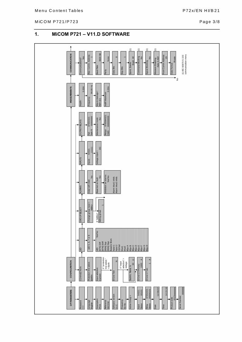
Menu Content Tables P72x/EN HI/B21 MiCOM P721/P723 Page 3/8
1. MiCOM P721 – V11.D SOFTWARE
OP
PARA
MET
ERS
Pass
wor
dC
ON
NEC
TIO
NLE
DG
ROU
P SE
LEC
TA
LARM
SIN
PUTS
OU
TPU
T RE
LAYS
INdi
ff=
Com
mun
icat
ions
?**
**
0.0
0AYe
s
Lang
uage
Prot
ectio
n lin
e se
lect
.LE
D 5
, 6, 7
or
8C
hang
e gr
oup
inpu
t =In
stal
sel
f-re
set
Inpu
ts
5
4321
Fail
876
5432
1Fr
eque
ncy
Rear
Com
m. A
ddre
ssEn
glis
hEA
RTH
MEN
UN
o11
111
Safe
R.
00
0000
0099
.99
Hz
1
Des
crip
tion
Inpu
t sel
ectio
nLE
D
Yes
/No
If “M
ENU
”Re
set l
ed o
n fa
ult
Volta
ge in
put =
Mai
nten
ance
mod
eM
ax &
Ave
rage
IBa
ud R
ate
P723
Cur
rent
[87N
] Diff
Setti
ng g
roup
No
DC
No
RST=
[C]
9600
Bd[8
7N] t
Diff
1Re
fere
nce
[95N
] Sup
Inhi
bitio
n on
ala
rms
Rela
ys
876
5W43
21In
diff
Max
imum
Pari
tyM
iCO
M[9
5N] t
Sup
Yes/
No
CM
D
00
0000
000
0
.00A
Non
eBu
swire
Sho
rt.
Softw
are
vers
ion
E/G
nd T
ext
Inpu
t 1A
larm
tAux
1 in
hib.
Dat
a Bi
ts11
.CN
Inpu
t 2A
larm
tAux
2 in
hib.
8C
B Fa
ilFr
eque
ncy
tAux
1St
op B
its50
Hz
tAux
21
tEqu
.AA
ctiv
e G
roup
=St
abili
z. R
esis
t. N
tEqu
.BSp
ont,
Even
ts(1
)1
30Ω
tEqu
.CEn
abl.
All
tEqu
.DIn
put
5432
1E/
Gnd
CT
Prim
ary
tEqu
.EC
omm
and
Bloc
king
(1)
Stat
us
0
0101
1000
AtE
qu.F
No
tEqu
.GRe
lay
876
5432
1E/
Gnd
CT
sec
tEqu
.HSi
gnal
Blo
ckin
g(1
)St
atus
000
0010
11
AN
o
Dat
eM
easu
re E
nabl
ing
(1)
11/0
6/07
Asd
u 3,
4&9
Tim
eFr
ont C
omm
Add
ress
14:1
5:16
29
Prod
uct c
ode
Dat
e Fo
rmat
P723
xxxx
xxxx
xPr
ivat
eN
oSe
rial N
umbe
rXX
XXXX
X(1
) IEC
608
70-5
-103
com
mun
icat
ion
men
u
CO
MM
UN
ICA
TIO
NM
EASU
REM
ENTS
CO
NFI
GU
RATI
ON
if “p
rote
ctio
n lin
e se
lect
.”
=Ea
rth
if “i
nput
se
lect
ion"
=
Volta
ge

P72x/EN HI/B21 Menu Content Tables Page 4/8 MiCOM P721/P723
[87N
] EA
RTH
DIF
F [9
5N] E
ART
H B
US-
WIR
ETR
IP C
OM
MA
ND
SLA
TCH
FU
NC
TIO
NS
BLO
CKI
NG
LO
GIC
1/2
OU
TPU
T RE
LAYS
LATC
H O
UTP
UT
PRO
TEC
TIO
NSU
PERV
ISIO
NRE
LAYS
[87N
] Ear
th d
iff p
rot?
[95N
] Ear
th b
us-w
ire s
up?
CB
Ope
ratin
g Ti
me
Latc
h
Ye
s/no
Bloc
k 1
/ 2
Y
es/N
oTr
ip
8
7654
321
Latc
h
4
32N
oN
o0.
1s
[87N
] tD
iff10
1010
1Re
lays
000
tAux
1[8
7N] t
Diff
[87N
] Diff
[87N
] Thr
esho
ld I
Diff
=[9
5N] T
hres
hold
I Su
p=Tr
ip
Yes
/No
tAux
2tA
ux1
[87N
] tD
iff1
In1
In[8
7N] t
Diff
Con
trol
Trip
tAux
2[9
5N] S
uptA
ux1
tEqu
. A[9
5N] t
Sup
[87N
] Thr
esho
ld V
Diff
=95
N] T
hres
hold
V S
up=
tAux
2tE
qu. B
CB
Fail
200.
0
V20
0.0
VC
ontr
ol T
riptE
qu. C
tAux
1tE
qu. A
tEqu
. DtA
ux2
[87N
] Flt
Tim
er t
Diff
[95N
] Flt
Tim
er t
Sup=
tEqu
. BtE
qu. E
Act
ive
Gro
up3.
0s
3.0
stE
qu. C
tEqu
. FC
ontr
ol T
riptE
qu. D
tEqu
. GIn
put1
[87N
] Mea
sure
Filt
er[9
5N] M
easu
re F
ilter
tEqu
. EtE
qu. H
Inpu
t2Sa
mpl
eSa
mpl
etE
qu. F
tEqu
. AtE
qu. G
tEqu
. B[8
7N] R
st T
imer
tRes
et=
[95N
] Rst
Tim
er tR
eset
=tE
qu. H
tEqu
. C0
s0
stE
qu. D
tEqu
. EtE
qu. F
No
No
tEqu
. GtE
qu. H
PRO
TEC
TIO
N G
1 /
G2
AU
TOM
AT.
CTR
L

Menu Content Tables P72x/EN HI/B21 MiCOM P721/P723 Page 5/8
INPU
TSC
IRC
UIT
BRE
AKE
R FA
ILLO
GIC
EQ
UA
TIO
NS
FAU
LT R
ECO
RDIN
STA
NTA
NEO
US
DIS
TURB
AN
CE
REC
ORD
SRE
CO
RDS
Inpu
ts 1
/2A
ux T
imes
CB
Fail
Equa
tion
Faul
t Rec
ord
Num
ber
Pre-
Tim
eN
oA
/B/C
/D/E
/F/G
/H25
51.
3s
Unl
atch
Aux
1 T
ime
tAux
1I d
iff <
=Eq
uatio
n A
.00
Faul
t Tim
eH
our
Post
-Tim
eA
ux1
0s
0.1
In(B
oole
an)
(Lo
gic)
00:
00:0
0:00
00:
00:0
0:00
2.0
sA
ux2
Star
t Dis
turb
Aux
2 T
ime
tAux
2C
B Fa
il Ti
me
tBF
Faul
t Dat
eD
ate
Dis
turb
Rec
Trig
Star
t Blo
ck L
ogic
10
s0.
1s
0
0/00
/00
0
0/00
/00
On
Inst
Star
t Blo
ck L
ogic
2C
hang
e se
tting
Equa
tion
A.1
5A
ctiv
e Se
t Gro
upO
rigin
Rese
t Led
s=
(
oper
and)
2
[8
7] tD
iffM
aint
. Mod
eLo
cal m
ode
T O
pera
teFa
ulte
d Ph
ase
Leng
thSy
nchr
o0
s
Ear
th00
0m
s
T Re
set
Thre
shol
dTr
ip0
s
[8
7] tD
iffYe
s
Faul
t Mag
nitu
de00
0A
Ie D
iff R
.M.S
000
A
REC
ORD
S
s ab
ove
from
.01
to A
.15
A A

P72x/EN HI/B21 Menu Content Tables Page 6/8 MiCOM P721/P723
2. MiCOM P723 – V11.D SOFTWARE
OP
PARA
MET
ERS
Pass
wor
dC
ON
NEC
TIO
NLE
DG
ROU
P SE
LEC
TA
LARM
SIN
PUTS
OU
TPU
T RE
LAYS
Com
mun
icat
ions
?**
**Ye
s
Lang
uage
Prot
ectio
n lin
e se
lect
.LE
D 5
, 6, 7
or
8C
hang
e gr
oup
inpu
t =In
stal
sel
f-re
set
Inpu
ts
5
4321
Fail
876
5432
1Id
iff=
0.
00A
Rear
Com
m. A
ddre
ssEn
glis
hEA
RTH
MEN
UN
o
1
1 1
1 1
Safe
R.
00
0000
000.
00A
0.0
0A1
Des
crip
tion
Inpu
t sel
ectio
nLE
D
Yes
/No
If “M
ENU
”Re
set l
ed o
n fa
ult
Volta
ge in
put =
Mai
nten
ance
mod
eFr
eque
ncy
Baud
Rat
eP7
23C
urre
nt[8
7/87
N] D
iff(1
)Se
tting
gro
upN
oD
CN
o99
.99
Hz
9600
Bd[8
7/87
N] t
Diff
(1)
1Re
fere
nce
[87C
Z] C
heck
Zon
eIn
hibi
tion
on a
larm
sRe
lays
8
765W
4321
Max
& A
vera
ge I
Pari
tyM
iCO
M[9
5/95
N] S
up(1
)Ye
s/N
oC
MD
0000
0000
0RS
T=[C
]N
one
[95/
95N
] tSu
p(1
)So
ftwar
e ve
rsio
nE/
Gnd
Tex
tBu
swir
e Sh
ort.
Ala
rm tA
ux1
inhi
b.Id
iffM
=
0.
00A
Dat
a Bi
ts11
.CN
[95A
] tSu
p A
Ala
rm tA
ux2
inhi
b.0.
00A
0.0
0A8
[95B
] tSu
p B
Ala
rm tA
ux3
inhi
b.Fr
eque
ncy
[95C
] tSu
p C
Ala
rm tA
ux4
inhi
b.St
op B
its50
Hz
Inpu
t 11
Inpu
t 2A
ctiv
e G
roup
=St
abili
z. R
esis
t. N
Inpu
t 3IN
diff=
Sp
ont,
Even
ts(1
)1
30Ω
Inpu
t 4
0.0
0AEn
abl.
All
Inpu
t 5In
put
5432
1E/
Gnd
CT
Prim
ary
CB
Fail
Freq
uenc
yC
omm
and
Bloc
king
(1)
Stat
us
0
0101
1000
AtA
ux1
99.9
9H
zN
otA
ux2
Rela
y
8
7654
321
E/G
nd C
T se
ctA
ux3
Max
& A
vera
ge I
Sign
al B
lock
ing
(1)
Stat
us
0
0000
101
1A
tAux
4RS
T=[C
]N
otE
qu.A
Dat
etE
qu.B
Indi
ff M
axim
umM
easu
re E
nabl
ing
(1)
11/0
6/07
tEqu
.C
0.0
0AA
sdu
3,4&
9tE
qu.D
Tim
ePh
ases
Tex
ttE
qu.E
Fron
t Com
m A
ddre
ss14
:15:
16L1
, L2,
L3
tEqu
.F29
tEqu
.GPr
oduc
t cod
etE
qu.H
Dat
e Fo
rmat
P723
xxxx
xxxx
xPr
ivat
e(1
) dep
endi
ng o
f pro
tect
ion
Seri
al N
umbe
rSt
abili
zing
Res
isto
r L1
line
conf
igur
atio
nXX
XXXX
X30
Ω(1
) IEC
608
70-5
-103
com
mun
icat
ion
men
uSt
abili
zing
Res
isto
r L2
30Ω
Stab
ilizi
ng R
esis
tor
L330
Ω
Line
CT
Prim
ary 10
00A
Line
CT
sec
1A
CO
MM
UN
ICA
TIO
NM
EASU
REM
ENTS
CO
NFI
GU
RATI
ON
if “p
rote
ctio
n lin
e se
lect
.”
=Ea
rth
if “c
onfig
urat
ion
/ pr
otec
tion
line
sele
ct.”
=Ea
rth
if “c
onfig
urat
ion/
pr
otec
tion
line
sele
ct.”
=ph
ase
if “i
nput
se
lect
ion"
=
Volta
ge
if “i
nput
se
lect
ion"
=
Volta
ge
if “p
rote
ctio
n lin
e se
lect
.”
=ph
ase
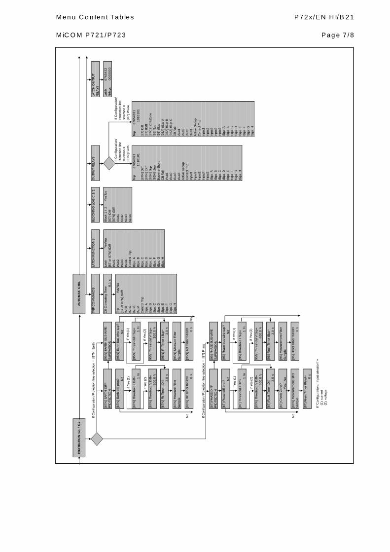
Menu Content Tables P72x/EN HI/B21 MiCOM P721/P723 Page 7/8
If C
onfig
urat
ion/
Prot
ectio
n lin
e se
lect
ion
= [8
7N] E
arth
TRIP
CO
MM
AN
DS
LATC
H F
UN
CTI
ON
SBL
OC
KIN
G L
OG
IC 1
/2O
UTP
UT
RELA
YSLA
TCH
OU
TPU
TRE
LAYS
[87N
] EA
RTH
DIF
F [9
5N] E
ART
H B
US-
WIR
EC
B O
pera
ting
Tim
eLa
tch
Yes/
noBl
ock
1 /
2
Yes
/No
Latc
h
8
7654
32PR
OTE
CTI
ON
SUPE
RVIS
ION
0.1
s[8
7 or
87N
] tD
iff[8
7] tD
iffRe
lays
000
0000
tAux
1[8
7N] t
Diff
[87N
] Ear
th d
iff p
rot?
[95N
] Ear
th b
us-w
ire s
up?
Trip
Y
es/N
otA
ux2
tAux
1N
oN
o[8
7 or
87N
] tD
if
ftA
ux3
tAux
2tA
ux1
tAux
4tA
ux3
tAux
2C
ontr
ol T
riptA
ux4
[87N
] Thr
esho
ld I
Diff
=[9
5N] T
hres
hold
I Su
p=tA
ux3
tEqu
. ATr
ip
8
7654
321
Trip
876
5432
11
In1
IntA
ux4
tEqu
. B10
1010
110
1010
1C
ontr
ol T
riptE
qu. C
[87N
] Diff
[87]
Diff
tEqu
. AtE
qu. D
[87N
] tD
iff[8
7] tD
iff[8
7N] T
hres
hold
V D
iff=
95N
] Thr
esho
ld V
Sup
=tE
qu. B
tEqu
. E[9
5N] S
up[8
7CZ]
Chk
Zone
200.
0V
200.
0V
tEqu
. CtE
qu. F
[95N
] tSu
p[9
5] S
uptE
qu. D
tEqu
. GBu
swire
-Sho
rt[9
5] tS
up[8
7N] F
lt Ti
mer
t D
iff[9
5N] F
lt Ti
mer
t Su
p=tE
qu. E
tEqu
. HC
B Fa
il[9
5A] t
Sup
A3.
0s
3.0
stE
qu. F
tAux
1[9
5A] t
Sup
BtE
qu. G
tAux
2[9
5A] t
Sup
C[8
7N] M
easu
re F
ilter
[95N
] Mea
sure
Filt
ertE
qu. H
tAux
3C
B Fa
ilSa
mpl
eSa
mpl
etA
ux4
tAux
1A
ctiv
e G
roup
tAux
2N
o[8
7N] R
st T
imer
tRes
et=
[95N
] Rst
Tim
er tR
eset
=C
ontr
ol T
riptA
ux3
0s
0s
No
Inpu
t1tA
ux4
Inpu
t2A
ctiv
e G
roup
Inpu
t3C
ontro
l Trip
If C
onfig
urat
ion/
Prot
ectio
n lin
e se
lect
ion
= [8
7] P
hase
Inpu
t4In
put1
Inpu
t5In
put2
[87]
PH
ASE
DIF
F [9
5] P
HA
SE B
US-
WIR
EtE
qu. A
Inpu
t3PR
OTE
CTI
ON
SUPE
RVIS
ION
tEqu
. BIn
put4
tEqu
. CIn
put5
[87]
Pha
se d
iff p
rot?
[95]
Pha
se b
us-w
ire s
up?
tEqu
. DtE
qu. A
No
No
tEqu
. EtE
qu. B
tEqu
. FtE
qu. C
tEqu
. GtE
qu. D
[87]
Thr
esho
ld I
Diff
=[9
5] T
hres
hold
I Su
p=tE
qu. H
tEqu
. E1
In1
IntE
qu. F
tEqu
. GtE
qu. H
[87N
] Thr
esho
ld V
Diff
=95
N] T
hres
hold
V S
up=
400.
0V
400.
0V
[87]
Fau
lt Ti
mer
tDiff
[95]
Fau
lt Ti
mer
tSup
=3.
0s
3.0
s
[87]
Che
ck Z
one?
[95]
Mea
sure
men
t Filt
erYe
s /
No
Sam
ple
No
[87N
] Mea
sure
men
t Filt
er[9
5] R
eset
Tim
er tR
eset
=Sa
mpl
e0
s
[87]
Res
et T
imer
tRes
et= 0s
If "C
onfig
urat
ion
/ In
put s
elec
tion"
=
(1):
cur
rent
AU
TOM
AT.
CTR
LPR
OTE
CTI
ON
G1 /
G2
(2
): v
olta
ge
If C
onfig
urat
ion/
Prot
ectio
n lin
e se
lect
ion
=
[87N
] Ear
th
If C
onfig
urat
ion/
Prot
ectio
n lin
e se
lect
ion
=
[87]
Pha
seif
Yes
(1)
if Ye
s (2
)
if Ye
s (1
)
if Ye
s (2
)
if Ye
s (1
)
if Ye
s (2
)
if Ye
s (1
)
if Ye
s (2
)
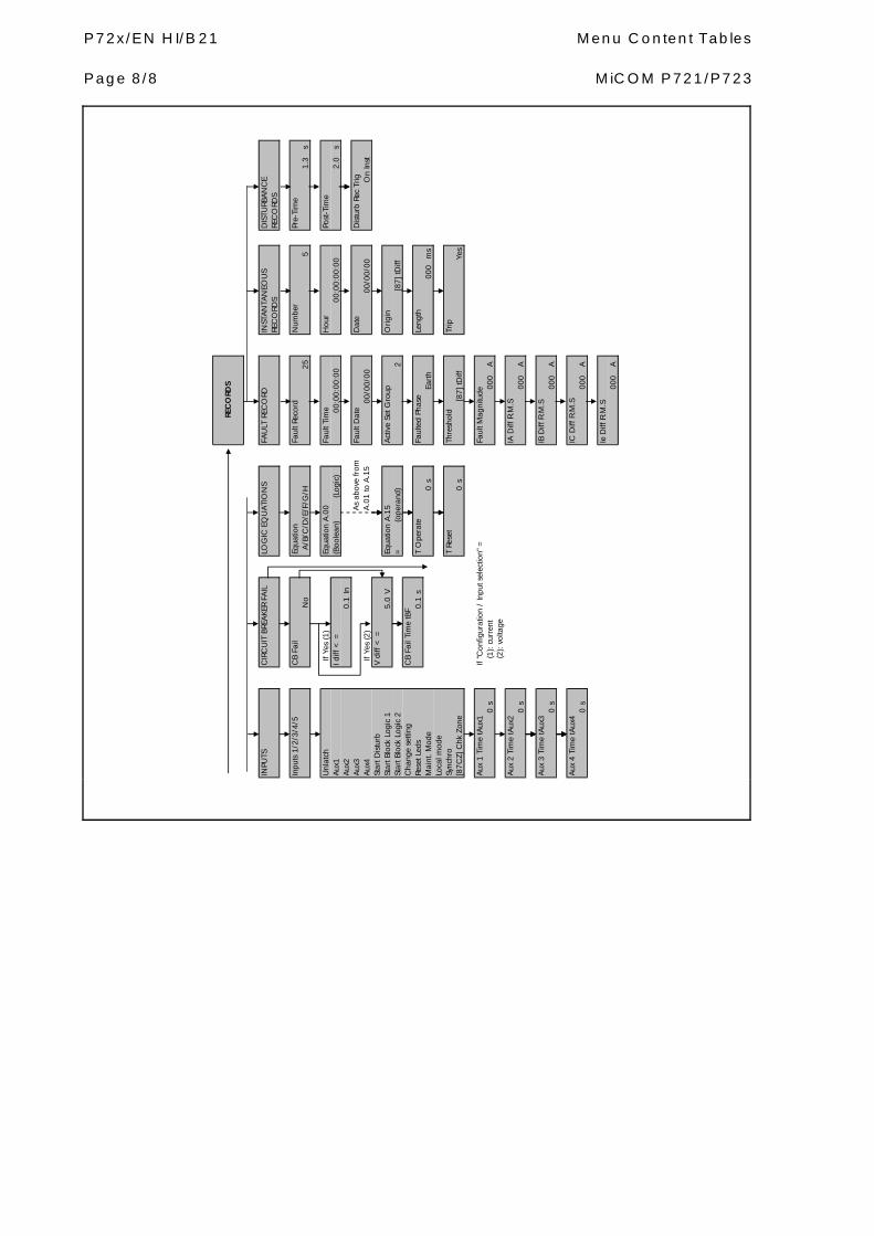
P72x/EN HI/B21 Menu Content Tables Page 8/8 MiCOM P721/P723
00:0
0:00
:00
2.0
s
INPU
TSC
IRC
UIT
BRE
AKE
R FA
ILLO
GIC
EQ
UA
TIO
NS
FAU
LT R
ECO
RDIN
STA
NTA
NEO
US
DIS
TURB
AN
CE
REC
ORD
SRE
CO
RDS
Inpu
ts 1
/2/3
/4/5
CB
Fail
Equa
tion
Faul
t Rec
ord
Num
ber
Pre-
Tim
eN
oA
/B/C
/D/E
/F/G
/H25
51.
3s
Unl
atch
If Y
es (1
)
Equa
tion
A.0
0Fa
ult T
ime
Hou
rPo
st-T
ime
Aux
1I d
iff <
=(B
oole
an)
(Lo
gic)
00:
00:0
0:00
A
ux2
0.1
InA
ux3
Faul
t Dat
eD
ate
Dis
turb
Rec
Trig
Aux
4 I
f Yes
(2)
00/
00/0
0
00/
00/0
0O
n In
stSt
art D
istu
rbV
diff
< =
Star
t Blo
ck L
ogic
15.
0V
Equa
tion
A.1
5A
ctiv
e Se
t Gro
upO
rigin
Star
t Blo
ck L
ogic
2=
(
oper
and)
2
[8
7] tD
iffC
hang
e se
tting
CB
Fail
Tim
e tB
FRe
set L
eds
0.1
sT
Ope
rate
Faul
ted
Phas
eLe
ngth
Mai
nt. M
ode
0s
E
arth
000
ms
Loca
l mod
eSy
nchr
oT
Rese
tTh
resh
old
Trip
[87C
Z] C
hk Z
one
0s
[87]
tDiff
Yes
A A A A
Aux
1 T
ime
tAux
1If
"Con
figur
atio
n /
Inpu
t sel
ectio
n" =
Faul
t Mag
nitu
de0
s
(1):
cur
rent
000
Aux
2 T
ime
tAux
2IA
Diff
R.M
.S0
s00
0
Aux
3 T
ime
tAux
3IB
Diff
R.M
.S0
s00
0
Aux
4 T
ime
tAux
4IC
Diff
R.M
.S0
s00
0
Ie D
iff R
.M.S
000
A
(2
): v
olta
ge
REC
ORD
S
s ab
ove
from
.01
to A
.15
A A

Technical Data P72x/EN TD/A11 MiCOM P721/P723
TECHNICAL DATA


Technical Data P72x/EN TD/A11 MiCOM P721/P723 Page 1/18
CONTENT
1. RATINGS 3
1.1 Power Supply 3 1.2 Frequency 3 1.3 Current Inputs 3 1.4 Phase and earth current transformers consumption 3 1.4.1 P72x phase CT consumption 3 1.4.2 P72x earth CT consumption 4 1.5 Logic Inputs 4 1.5.1 Supply 4 1.6 Output Relay Characteristic 5
2. INSULATION 5
3. EMC TESTS 6
4. ENVIRONMENT 7
5. EU DIRECTIVE 8
5.1 EMC compliance 8 5.2 Product safety 8
6. DEVIATION OF PROTECTION ELEMENTS 9
7. DEVIATION OF AUTOMATION FUNCTIONS TIMERS 9
8. DEVIATION OF MEASUREMENTS 9
9. PROTECTION SETTING RANGES 10
9.1 [87N] Earth differential protection 10 9.1.1 Protection Setting Ranges 10 9.2 [95N] Earth bus-wire supervision 10 9.2.1 Protection Setting Ranges 10 9.3 [87] Phase differential protection (P723 only) 10 9.3.1 Protection Setting Ranges 10 9.4 [95] Phase bus-wire supervision (P723 only) 11 9.4.1 Protection Setting Ranges 11

P72x/EN TD/A11 Technical Data Page 2/18 MiCOM P721/P723
10. AUTOMATION CONTROL FUNCTIONS 12
10.1 Trip commands 12 10.2 Latch functions 12 10.3 Blocking logic 12 10.4 Output relays 12 10.5 Latch of the auxiliary output relays 12 10.6 Inputs 12 10.6.1 Inputs assignation 12 10.6.2 Auxiliary timers 12 10.7 Circuit Breaker Failure 13 10.7.1 CB Fail Setting Ranges 13 10.8 Logic Equations 13 10.8.1 Timer Setting Ranges 13 10.8.2 Available logical gates 14 10.8.3 Available signals 14
11. RECORDING FUNCTIONS 16
11.1 Fault Record 16 11.2 Instantaneous recorder 16 11.3 Disturbance Records 16 11.3.1 Triggers; Data; Setting Ranges 16
12. COMMUNICATION 17
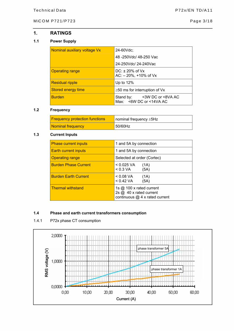
Technical Data P72x/EN TD/A11 MiCOM P721/P723 Page 3/18
1. RATINGS 1.1 Power Supply
Nominal auxiliary voltage Vx 24-60Vdc;
48 -250Vdc/ 48-250 Vac
24-250Vdc/ 24-240Vac
Operating range DC: ± 20% of Vx AC: – 20%, +10% of Vx
Residual ripple Up to 12%
Stored energy time ≥50 ms for interruption of Vx
Burden Stand by: <3W DC or <8VA AC Max: <6W DC or <14VA AC
1.2 Frequency
Frequency protection functions nominal frequency ±5Hz
Nominal frequency 50/60Hz
1.3 Current Inputs
Phase current inputs 1 and 5A by connection
Earth current inputs 1 and 5A by connection
Operating range Selected at order (Cortec)
Burden Phase Current < 0.025 VA (1A) < 0.3 VA (5A)
Burden Earth Current < 0.08 VA (1A) < 0.42 VA (5A)
Thermal withstand 1s @ 100 x rated current 2s @ 40 x rated current continuous @ 4 x rated current
1.4 Phase and earth current transformers consumption
1.4.1 P72x phase CT consumption
phase transformer 5A
RM
S vo
ltage
(V)
Current (A)
phase transformer 1A
phase transformer 5A
RM
S vo
ltage
(V)
Current (A)
phase transformer 1A

P72x/EN TD/A11 Technical Data Page 4/18 MiCOM P721/P723 1.4.2 P72x earth CT consumption
earth transformer 5A
RM
S vo
ltage
(V)
Current (A)
earth transformer 1A
earth transformer 5A
RM
S vo
ltage
(V)
Current (A)
earth transformer 1A
1.5 Logic Inputs
Logic input type Independent optically insulated
Logic input burden < 10 mAmps per input
Logic input recognition time (DC inputs)
< 5ms in a 50Hz system
< 4ms in a 60Hz system
Logic input recognition time (AC inputs)
<7ms in a 50Hz system
< 6ms in a 60Hz system
Logic input recognition time (ENA inputs)
<15ms in a 50Hz system
< 12ms in a 60Hz system
1.5.1 Supply
Relay auxiliary power supply Logic Inputs
Ordering Code
Nominal voltage range
Vx
Operating voltage range
Nominal Voltage range
Minimal polarisation
voltage
Maximum polarisation
current
Holding current
after 2 ms
Maximum continuous withstand
A 24 - 60 Vdc 19,2 – 76 Vdc 24 – 250 Vdc24 – 240 Vac
19,2 Vdc 19,2 Vac
35 mA
2.3 mA
300 Vdc 264 Vac
T 48 – 250 Vdc 48 – 240 Vac
Special EA (**)
38.4 – 300 Vdc 38.4 – 264 Vac
24 – 250 Vdc24 – 240 Vac
19,2 Vdc 19,2 Vac
35 mA
2.3 mA
300 Vdc 264 Vac
Z 24 – 250 Vdc 24 – 250 Vac
19,2 – 300 Vdc 19.2 – 264 Vac
24 – 250 Vdc24 – 240 Vac
19,2 Vdc 19,2 Vac 35 mA 2.3 mA 300 Vdc
264 Vac
(**) Logic input recognition time for EA approval. Dedicated filtering on 24 samples (15 ms at 50 Hz)
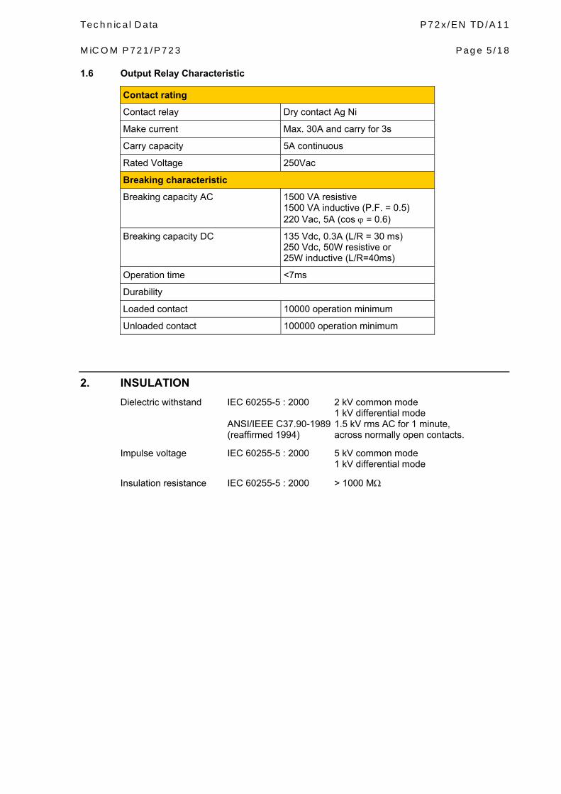
Technical Data P72x/EN TD/A11 MiCOM P721/P723 Page 5/18 1.6 Output Relay Characteristic
Contact rating
Contact relay Dry contact Ag Ni
Make current Max. 30A and carry for 3s
Carry capacity 5A continuous
Rated Voltage 250Vac
Breaking characteristic
Breaking capacity AC 1500 VA resistive 1500 VA inductive (P.F. = 0.5) 220 Vac, 5A (cos ϕ = 0.6)
Breaking capacity DC 135 Vdc, 0.3A (L/R = 30 ms) 250 Vdc, 50W resistive or 25W inductive (L/R=40ms)
Operation time <7ms
Durability
Loaded contact 10000 operation minimum
Unloaded contact 100000 operation minimum
2. INSULATION Dielectric withstand IEC 60255-5 : 2000 2 kV common mode 1 kV differential mode ANSI/IEEE C37.90-1989 1.5 kV rms AC for 1 minute, (reaffirmed 1994) across normally open contacts.
Impulse voltage IEC 60255-5 : 2000 5 kV common mode 1 kV differential mode
Insulation resistance IEC 60255-5 : 2000 > 1000 MΩ
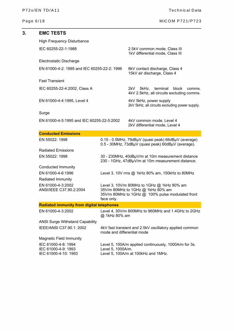
P72x/EN TD/A11 Technical Data Page 6/18 MiCOM P721/P723
3. EMC TESTS High Frequency Disturbance
IEC 60255-22-1:1988 2.5kV common mode, Class III 1kV differential mode, Class III
Electrostatic Discharge
EN 61000-4-2: 1995 and IEC 60255-22-2: 1996 8kV contact discharge, Class 4 15kV air discharge, Class 4
Fast Transient
IEC 60255-22-4:2002, Class A 2kV 5kHz, terminal block comms. 4kV 2.5kHz, all circuits excluding comms.
EN 61000-4-4:1995, Level 4 4kV 5kHz, power supply 2kV 5kHz, all circuits excluding power supply.
Surge
EN 61000-4-5:1995 and IEC 60255-22-5:2002 4kV common mode, Level 4 2kV differential mode, Level 4
Conducted Emissions EN 55022: 1998 0.15 - 0.5MHz, 79dBµV (quasi peak) 66dBµV (average)
0.5 - 30MHz, 73dBµV (quasi peak) 60dBµV (average). Radiated Emissions EN 55022: 1998 30 - 230MHz, 40dBµV/m at 10m measurement distance
230 - 1GHz, 47dBµV/m at 10m measurement distance. Conducted Immunity EN 61000-4-6:1996 Level 3, 10V rms @ 1kHz 80% am, 150kHz to 80MHz Radiated Immunity EN 61000-4-3:2002 ANSI/IEEE C37.90.2:2004
Level 3, 10V/m 80MHz to 1GHz @ 1kHz 80% am 35V/m 80MHz to 1GHz @ 1kHz 80% am 35V/m 80MHz to 1GHz @ 100% pulse modulated front face only.
Radiated immunity from digital telephones EN 61000-4-3:2002 Level 4, 30V/m 800MHz to 960MHz and 1.4GHz to 2GHz
@ 1kHz 80% am ANSI Surge Withstand Capability IEEE/ANSI C37.90.1: 2002 4kV fast transient and 2.5kV oscillatory applied common
mode and differential mode Magnetic Field Immunity IEC 61000-4-8: 1994 IEC 61000-4-9: 1993 IEC 61000-4-10: 1993
Level 5, 100A/m applied continuously, 1000A/m for 3s. Level 5, 1000A/m. Level 5, 100A/m at 100kHz and 1MHz.
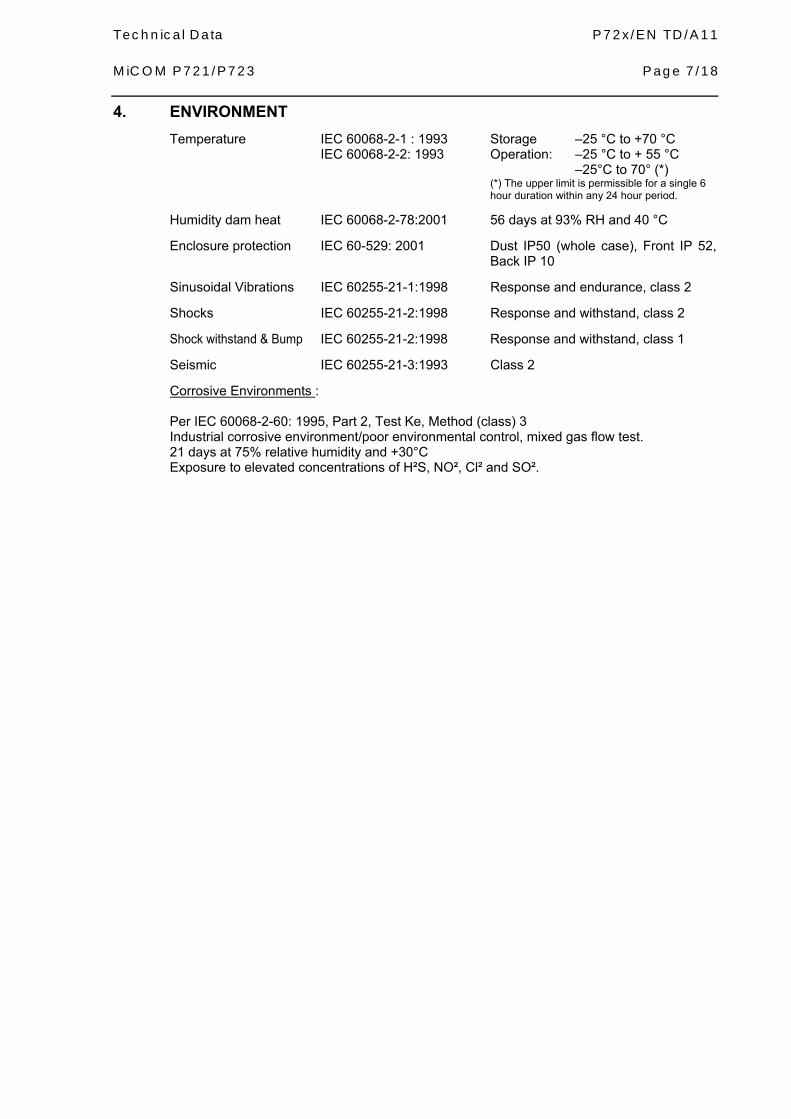
Technical Data P72x/EN TD/A11 MiCOM P721/P723 Page 7/18
4. ENVIRONMENT Temperature IEC 60068-2-1 : 1993 Storage –25 °C to +70 °C IEC 60068-2-2: 1993 Operation: –25 °C to + 55 °C –25°C to 70° (*) (*) The upper limit is permissible for a single 6 hour duration within any 24 hour period.
Humidity dam heat IEC 60068-2-78:2001 56 days at 93% RH and 40 °C
Enclosure protection IEC 60-529: 2001 Dust IP50 (whole case), Front IP 52, Back IP 10
Sinusoidal Vibrations IEC 60255-21-1:1998 Response and endurance, class 2
Shocks IEC 60255-21-2:1998 Response and withstand, class 2
Shock withstand & Bump IEC 60255-21-2:1998 Response and withstand, class 1
Seismic IEC 60255-21-3:1993 Class 2
Corrosive Environments : Per IEC 60068-2-60: 1995, Part 2, Test Ke, Method (class) 3 Industrial corrosive environment/poor environmental control, mixed gas flow test. 21 days at 75% relative humidity and +30°C Exposure to elevated concentrations of H²S, NO², Cl² and SO².

P72x/EN TD/A11 Technical Data Page 8/18 MiCOM P721/P723
5. EU DIRECTIVE 5.1 EMC compliance
89/336/EEC
93/31/EEC Compliance with European Commission EMC Directive.
Generic standards were used to establish conformity:
EN50081-2: 1994
EN60952-2: 1995
5.2 Product safety
2006/95/EC
(replacing 73/23/EEC from 01/2007) Compliance with European Commission Low Voltage Directive. Compliance is demonstrated by reference to generic safety standards:
− EN61010-1: 1993/A2: 1995
− EN60950: 1992/A11: 1997

Technical Data P72x/EN TD/A11 MiCOM P721/P723 Page 9/18
6. DEVIATION OF PROTECTION ELEMENTS
Element Range Deviation Fault timer Reset timer
Earth differential protection I diff (V diff)
0.01In to 1In (0.5 to 200V)
± 2% 0s - 2s 0 to 600s
Phase differential protection I diff (V diff)
0.02 to 2In (1 to 400V)
± 2% 0s – 2s 0 to 600s
Earth bus-wire supervision
0.01 to 1 In (0.5 to 200V)
± 2% 0.5s – 3s 0 to 600s
Phase bus-wire supervision I Sup (V Sup)
0.01 to 1In (1 to 400V)
± 2% 0.5s – 3s 0 to 600s
7. DEVIATION OF AUTOMATION FUNCTIONS TIMERS
CB fail & CB monitoring timers ±2% 0-10s
Auxiliary timers tAUX1, tAUX2, tAUX3, tAUX4 ±2% 0-200s
8. DEVIATION OF MEASUREMENTS
Measurement Range Deviation
Phase current 0.02In to 10In Typical ±0.5% at In
Earth current 0.004In to 2In Typical ±0.5% at In

P72x/EN TD/A11 Technical Data Page 10/18 MiCOM P721/P723
9. PROTECTION SETTING RANGES 9.1 [87N] Earth differential protection
9.1.1 Protection Setting Ranges
Setting Range [87N] Earth differential protection Min Max Step
[87N] Earth differential protection
Yes / No
[87N] Threshold I diff 0.01In 1In 0.01In
[87N] Threshold V diff 0.5V 200V 0.1V
[87N] Filter timer t Diff 0s 2s 10ms
[87N] Reset timer tReset 0 600s 10ms
Measurement Filter Sample mode / Fast sample mode / Fourier mode
9.2 [95N] Earth bus-wire supervision
9.2.1 Protection Setting Ranges
Setting Range [95N] Earth bus-wire supervision Min Max Step
[95N] Earth bus-wire supervision Yes / No
[95N] Threshold I Sup 0.01In 1In 0.01In
[95N] Threshold V Sup 0.5V 200V 0.1V
[95N] Filter timer t Sup 0.5s 3s 10ms
[95N] Reset timer tReset 0 600s 10ms
Measurement Filter Sample mode / Fast sample mode / Fourier mode
9.3 [87] Phase differential protection (P723 only)
9.3.1 Protection Setting Ranges
Setting Range [87] Phase differential protection Min Max Step
[87] Phase differential protection Yes / No
[87] Threshold I diff 0.02In 2In 0.01In
[87] Threshold V diff 1V 400V 0.1V
[87] Filter timer t Diff 0s 2s 10ms
[87] Check zone? Yes / No
[87] Reset timer tReset 0 600s 10ms
Measurement Filter Sample mode / Fast sample mode / Fourier mode
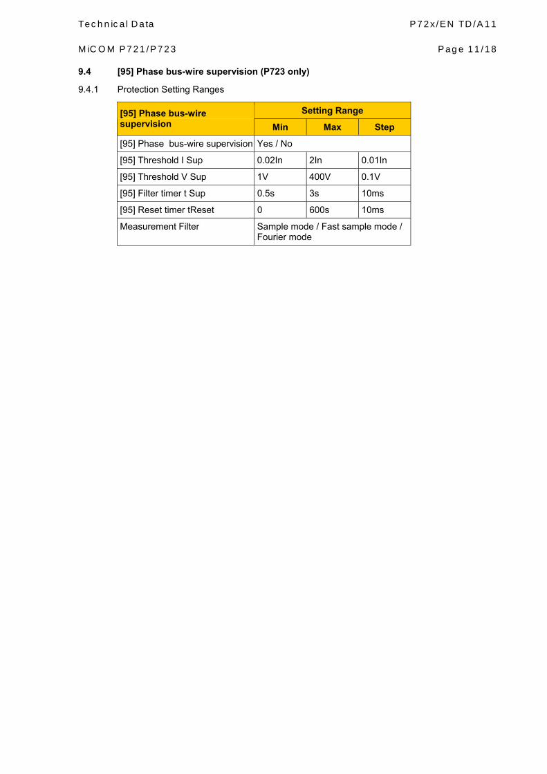
Technical Data P72x/EN TD/A11 MiCOM P721/P723 Page 11/18 9.4 [95] Phase bus-wire supervision (P723 only)
9.4.1 Protection Setting Ranges
Setting Range [95] Phase bus-wire supervision Min Max Step
[95] Phase bus-wire supervision Yes / No
[95] Threshold I Sup 0.02In 2In 0.01In
[95] Threshold V Sup 1V 400V 0.1V
[95] Filter timer t Sup 0.5s 3s 10ms
[95] Reset timer tReset 0 600s 10ms
Measurement Filter Sample mode / Fast sample mode / Fourier mode
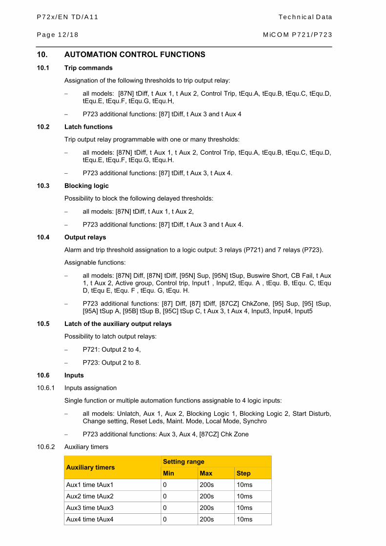
P72x/EN TD/A11 Technical Data Page 12/18 MiCOM P721/P723
10. AUTOMATION CONTROL FUNCTIONS 10.1 Trip commands
Assignation of the following thresholds to trip output relay:
− all models: [87N] tDiff, t Aux 1, t Aux 2, Control Trip, tEqu.A, tEqu.B, tEqu.C, tEqu.D, tEqu.E, tEqu.F, tEqu.G, tEqu.H,
− P723 additional functions: [87] tDiff, t Aux 3 and t Aux 4
10.2 Latch functions
Trip output relay programmable with one or many thresholds:
− all models: [87N] tDiff, t Aux 1, t Aux 2, Control Trip, tEqu.A, tEqu.B, tEqu.C, tEqu.D, tEqu.E, tEqu.F, tEqu.G, tEqu.H.
− P723 additional functions: [87] tDiff, t Aux 3, t Aux 4.
10.3 Blocking logic
Possibility to block the following delayed thresholds:
− all models: [87N] tDiff, t Aux 1, t Aux 2,
− P723 additional functions: [87] tDiff, t Aux 3 and t Aux 4.
10.4 Output relays
Alarm and trip threshold assignation to a logic output: 3 relays (P721) and 7 relays (P723).
Assignable functions:
− all models: [87N] Diff, [87N] tDiff, [95N] Sup, [95N] tSup, Buswire Short, CB Fail, t Aux 1, t Aux 2, Active group, Control trip, Input1 , Input2, tEqu. A , tEqu. B, tEqu. C, tEqu D, tEqu E, tEqu. F , tEqu. G, tEqu. H.
− P723 additional functions: [87] Diff, [87] tDiff, [87CZ] ChkZone, [95] Sup, [95] tSup, [95A] tSup A, [95B] tSup B, [95C] tSup C, t Aux 3, t Aux 4, Input3, Input4, Input5
10.5 Latch of the auxiliary output relays
Possibility to latch output relays:
− P721: Output 2 to 4,
− P723: Output 2 to 8.
10.6 Inputs
10.6.1 Inputs assignation
Single function or multiple automation functions assignable to 4 logic inputs:
− all models: Unlatch, Aux 1, Aux 2, Blocking Logic 1, Blocking Logic 2, Start Disturb, Change setting, Reset Leds, Maint. Mode, Local Mode, Synchro
− P723 additional functions: Aux 3, Aux 4, [87CZ] Chk Zone
10.6.2 Auxiliary timers
Setting range Auxiliary timers
Min Max Step
Aux1 time tAux1 0 200s 10ms
Aux2 time tAux2 0 200s 10ms
Aux3 time tAux3 0 200s 10ms
Aux4 time tAux4 0 200s 10ms

Technical Data P72x/EN TD/A11 MiCOM P721/P723 Page 13/18 10.7 Circuit Breaker Failure
10.7.1 CB Fail Setting Ranges
Setting range CB Fail
Min Max Step
CB Fail ? Yes or No
I Diff < 0.01 In 1In 0.01 In
V Diff < 0.5V 200V 100mV
CB Fail Time tBF 0 10s 0.01s
10.8 Logic Equations
The MiCOM P721 and P723 relays integrate complete logic equations to allow customization of the product based on customer application.
Up to 8 independent Boolean equations can be used (from A to H). Every result of equation can be time delayed and assigned to any output relays, trip, trip latching and/or HMI LEDs.
Up to 16 operands can be used (from 00 to 15). Within operands, there are two parts:
− (1/2) : logical gates (NOT, OR, AND, NOT AND, NOT OR)
− (2/2) : signals ([87N] Diff, [95N] tSup, tAux, input…etc)
10.8.1 Timer Setting Ranges
Setting range Logic equat T delay Min Max Step
EQU. A Toperat 0 s 600 s 0.01 s
EQU. A Treset 0 s 600 s 0.01 s
EQU. B Toperat 0 s 600 s 0.01 s
EQU. B Treset 0 s 600 s 0.01 s
EQU. C Toperat 0 s 600 s 0.01 s
EQU. C Treset 0 s 600 s 0.01 s
EQU. D Toperat 0 s 600 s 0.01 s
EQU. D Treset 0 s 600 s 0.01 s
EQU. E Toperat 0 s 600 s 0.01 s
EQU. E Treset 0 s 600 s 0.01 s
EQU. F Toperat 0 s 600 s 0.01 s
EQU. F Treset 0 s 600 s 0.01 s
EQU. G Toperat 0 s 600 s 0.01 s
EQU. G Treset 0 s 600 s 0.01 s
EQU. H Toperat 0 s 600 s 0.01 s
EQU. H Treset 0 s 600 s 0.01 s

P72x/EN TD/A11 Technical Data Page 14/18 MiCOM P721/P723
10.8.2 Available logical gates
Logical gates Availability (1/2)
NOT A00 B00 C00 D00 E00 F00 G00 H00
OR (by default)
AND
AND NOT
OR NOT
A01 to A15 B01 to B15 C01 to C15 D01 to D15 E01 to E15 F01 to F15 G01 to G15 H01 to H15
10.8.3 Available signals
With the Logic Equations submenu, 16 operands can be used in any single equation. The following logic signals are available for mapping to an equation:
TEXT Signals (2/2)
P721 and P723:
Null Condition is Null
Not Null Condition is not Null
[87N] Diff Earth differential protection threshold
[87N] tDiff Time delayed earth differential protection threshold
[95N] tSup Time delayed earth high impedance differential threshold (buswire supervision)
tAux 1 Copy of the status of the Logic Input tAux 1
tAux 2 Copy of the status of the Logic Input tAux 2
Input 1 Instantaneous digital input 1
Input 2 Instantaneous digital input 2
Group 2 Group 2 is active (setting)
CB Fail Circuit Breaker does not operate
P723 only:
[87] Diff Phase differential protection threshold
[87] tDiff Time delayed phase differential protection threshold
[87CZ] Check zone Check Zone status
[95] Sup Phase high impedance differential threshold (buswire supervision)
[95N] Sup Earth high impedance differential threshold (buswire supervision)
[95] tSup Time delayed phase high impedance differential threshold (buswire supervision)

Technical Data P72x/EN TD/A11 MiCOM P721/P723 Page 15/18
TEXT Signals (2/2)
[95A] tSupA Time delayed phase A (or L1, or R) high impedance differential threshold (buswire supervision)
[95B] tSupB As above for phase B (or L2 or S)
[95C] tSupC As above for phase C (or L3 or T)
Buswire Short Buswires short-circuited
tAux 3 Copy of the status of the Logic Input tAux 3
tAux 4 Copy of the status of the Logic Input tAux 4
Input 3 Instantaneous digital input 3
Input 4 Instantaneous digital input 4
Input 5 Instantaneous digital input 5
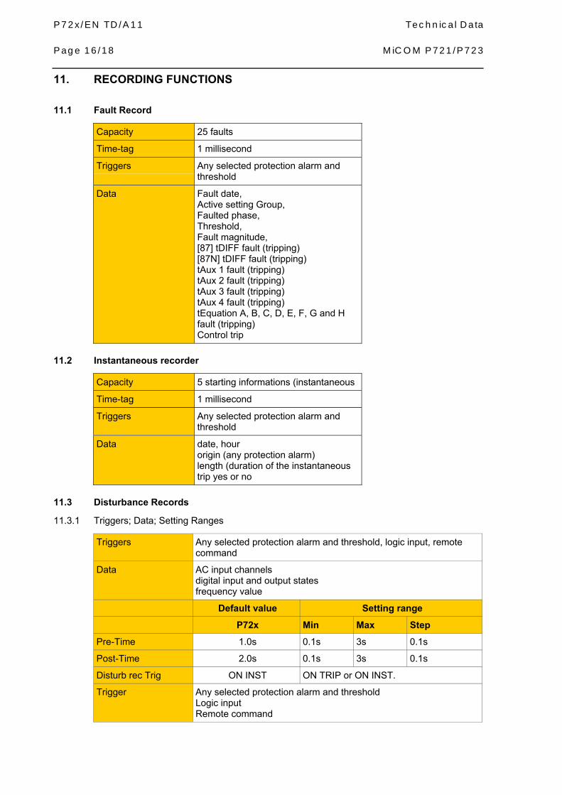
P72x/EN TD/A11 Technical Data Page 16/18 MiCOM P721/P723
11. RECORDING FUNCTIONS
11.1 Fault Record
Capacity 25 faults
Time-tag 1 millisecond
Triggers Any selected protection alarm and threshold
Data Fault date, Active setting Group, Faulted phase, Threshold, Fault magnitude, [87] tDIFF fault (tripping) [87N] tDIFF fault (tripping) tAux 1 fault (tripping) tAux 2 fault (tripping) tAux 3 fault (tripping) tAux 4 fault (tripping) tEquation A, B, C, D, E, F, G and H fault (tripping) Control trip
11.2 Instantaneous recorder
Capacity 5 starting informations (instantaneous
Time-tag 1 millisecond
Triggers Any selected protection alarm and threshold
Data date, hour origin (any protection alarm) length (duration of the instantaneous trip yes or no
11.3 Disturbance Records
11.3.1 Triggers; Data; Setting Ranges
Triggers Any selected protection alarm and threshold, logic input, remote command
Data AC input channels digital input and output states frequency value
Default value Setting range
P72x Min Max Step
Pre-Time 1.0s 0.1s 3s 0.1s
Post-Time 2.0s 0.1s 3s 0.1s
Disturb rec Trig ON INST ON TRIP or ON INST.
Trigger Any selected protection alarm and threshold Logic input Remote command

Technical Data P72x/EN TD/A11 MiCOM P721/P723 Page 17/18
12. COMMUNICATION
Type Port
Relay position Physical Link Connectors Data Rate Protocol
RS485 Rear port Screened twister pair
Screws or snap-on
300 to 38400 baud (programmable)
ModBus RTU, Courier, IEC60870-5-103, DNP3.0
RS232 Front port Screened twister pair
Sub–D 9 pin female connector
300 to 38400 baud (programmable)
ModBus RTU

P72x/EN TD/A11 Technical Data Page 18/18 MiCOM P721/P723
BLANK PAGE

Getting Started P72x/EN GS/B21_ MiCOM P721 / P723
GETTING STARTED


Getting Started P72x/EN GS/B21_ MiCOM P721 / P723 Page 1/30
CONTENT
1. ENERGISING THE RELAY 3
1.1 System Connections 3
1.2 Auxiliary Power Supply Connections 3
2. USER INTERFACE AND MENU STRUCTURE 4
2.1 User interfaces and menu structure 4
2.1.1 “Default settings” alarm 4
2.1.2 Password protection 4
2.1.3 Setting the language 5
2.1.4 Setting Date and time 5
2.1.5 Menu navigation 5
2.2 Menu structure 6
3. LOCAL CONNECTION TO A PC 6
3.1 Configuration 7
3.1.1 REMOTE connection 7
3.2 Products plugged in the same panel 8
3.3 Communication between distant products 8
3.4 MiCOM S1 and MiCOM S1 Studio relay communications basics 9
3.5 MiCOM S1 Studio 9
3.5.1 Data Model Management 9
3.5.2 “Quick Connection” to the relay using MiCOM S1 Studio 12
3.5.3 Create a system 15
3.5.4 Create a new substation 16
3.5.5 Create a new voltage level 17
3.5.6 Create a new bay 17
3.5.7 Create a new device 18
3.5.8 Open Settings File 19
3.6 MiCOM S1 21
3.6.1 Starting MiCOM S1 21
3.6.2 Open communication link with relay 23
3.6.3 Off-line use of MiCOM S1 25
3.6.4 MiCOM monitoring 25
3.7 Presentation and analysis of disturbance 27
4. WITHDRAWING MODULE FROM CASE 28
5. COMPANY CONTACT INFORMATION 30

P72x/EN GS/B21_ Getting Started Page 2/30 MiCOM P721 / P723
BLANK PAGE
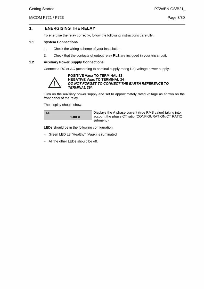
Getting Started P72x/EN GS/B21_ MiCOM P721 / P723 Page 3/30
1. ENERGISING THE RELAY
To energise the relay correctly, follow the following instructions carefully.
1.1 System Connections
1. Check the wiring scheme of your installation.
2. Check that the contacts of output relay RL1 are included in your trip circuit.
1.2 Auxiliary Power Supply Connections
Connect a DC or AC (according to nominal supply rating Ua) voltage power supply.
POSITIVE Vaux TO TERMINAL 33 NEGATIVE Vaux TO TERMINAL 34 DO NOT FORGET TO CONNECT THE EARTH REFERENCE TO TERMINAL 29!
Turn on the auxiliary power supply and set to approximately rated voltage as shown on the front panel of the relay.
The display should show:
IA 1.00 A
Displays the A phase current (true RMS value) taking into account the phase CT ratio (CONFIGURATION/CT RATIO submenu).
LEDs should be in the following configuration:
Green LED L3 "Healthy" (Vaux) is iluminated
All the other LEDs should be off.

P72x/EN GS/B21_ Getting Started Page 4/30 MiCOM P721 / P723
2. USER INTERFACE AND MENU STRUCTURE
Before carrying out any work on the equipment, the user should be familiar with the contents of the safety section/safety guide SFTY/4LM/D11 or later issue, the technical data section and the ratings on the equipment rating label.
Refer to “GETTING STARTED” (GS) section for the description of the following procedures (interfaces and menu).
Before the initial operation of the relay, some of the parameter settings must be checked or modified (otherwise, “Setting alarm” is displayed).
Lift the upper and lower hinged covers and remove the transparent cover over the front panel. When the keypad is exposed, it provides full access to the menu options of the relay. The relevant information is displayed on the LCD.
2.1 User interfaces and menu structure
The settings and functions of the MiCOM relay can be accessed both from the front panel keypad and LCD, and via the front and rear communication ports. Information on each of these methods is given in this section to describe how to start using the relay.
The front panel of the relay includes a keypad, a 16-character alphanumeric liquid crystal display (LCD) and 8 LEDs.
2.1.1 “Default settings” alarm
When the relay is powered ON, it checks its memory contents. If the default settings are loaded, an alarm is raised and The ALARM yellow LED lights up.
To suppress this message and to reset the watch dog, change one parameter in the relay's menu:
Press the button,
Modify, for instance, the password or the language (“OP parameters” menu.
2.1.2 Password protection
Password protection is applicable to most of the relay parameter settings, especially to the selection of the various thresholds, time delays, communication parameters, allocation of logic inputs and logic outputs.
The password consists of four capital characters. When leaving the factory, the password is set to AAAA. The user can define any combination of four characters.
Should the password be lost or forgotten, the modification of stored parameters is blocked. It is then necessary to contact the manufacturer or his agent and by specifying the serial number of the relay, a stand-by password specific to the relay concerned may be obtained.
NOTE: The programming mode is indicated with the letter "P" on the right hand side of the display on each menu heading. The letter "P" remains present as long as the password is active (5 minutes if there is no action on the keypad).
Go to the “OP. Parameters” menu by pressing and then to the “password” menu by pressing ,
Enter the current password (default password = “AAAA”) and validate with (this operation is not necessary if the password has been entered some minutes ago),
Enter the new password character by character, using and arrows to change a letter (maintain the key pressed to scroll through the letter in the alphabet). Use and arrows to select another character: a flashing cursor will indicate which character field of the password may be entered.,
Validate using or cancel using . If the password is correct, the following message is displayed on the LCD: PASSWORD OK

Getting Started P72x/EN GS/B21_ MiCOM P721 / P723 Page 5/30
As soon as the password has been entered, no setting change will be accepted via the remote or local communication port (RS485 or RS232).
Alternatively, the password can be entered by using the Password window in the OP.PARAMETERS menu. This password entry procedure is the same as above.
NOTE: In case of loss of password a back up password can be provided contacting Schneider Electric Customer Care Center.
2.1.3 Setting the language
Go to the “OP. Parameters” menu by pressing and then to the “Language” menu by pressing , ,
If necessary, enter the current password and validate with ,
Select the language using or arrows, and validate with ,
Validate using or cancel using .
2.1.4 Setting Date and time
Go to the “OP. Parameters” menu by pressing and then to the “Date” menu by pressing (x9),
If necessary, enter the current password and validate with ,
Set the date using or arrow, and validate with (10/11/08 means November 10th 2008),
NOTE: When you modify the date, the first digit for the day or the month can be selected according to the second digit. For instance, if 13/09/08 is displayed, you cannot select 33 for the day, or 29 for the month.
Validate using or cancel using .
Select the “Time ” menu by pressing 2 key,
Set the date using or arrow, and validate with (14:21:42 means 2:21:42 pm)
2.1.5 Menu navigation
A simple menu structure allows setting and reading of parameters and functionality.
The keypad provides full access to the menu options, with informations displayed on the LCD.
Press , , and keys for menu navigation:
Press or keys to navigate from a menu heading to another menu heading (refer to the figure below),
Press key to access to a sub menu, then navigate using or keys.
Maintain these keys pressed to scroll through the menu,
If necessary, modify a parameter by pressing key.
Modify the corresponding parameter using arrows,
Validate using , or cancel using .

P72x/EN GS/B21_ Getting Started Page 6/30 MiCOM P721 / P723 2.2 Menu structure
The menu structure is shown below.
DEFAULT DISPLAYI Diff = 1245 A
OP PARAMETERS MEASUREMENTS COMMUNICATION
PROTECTION G1/G2AUTOMAT. CTRLRECORDS
CONFIGURATION
Refer to the HI chapter for the menu details.

Getting Started P72x/EN GS/B21_ MiCOM P721 / P723 Page 7/30
3. LOCAL CONNECTION TO A PC
3.1 Configuration
MiCOM S1 Studio
P0107ENc
For a local connection between a PC and the relay, a serial cable with metallic shield should be used.
The wiring of the RS232 cable must be as shown in the following drawing.
1
2
3
4
5
6
7
8
9
1
2
3
4
5
6
7
8
9
RS232 PC PORT9 pin male connector
MiCOM P721/P7239 pin female connector
P0073ENb
A USB/RS232 cable can also be used to communicate to the relay
3.1.1 REMOTE connection
The figure shows the recommended way to connect a RS485 cable to the relay to build a local network.

P72x/EN GS/B21_ Getting Started Page 8/30 MiCOM P721 / P723 3.2 Products plugged in the same panel
RS485 cable
2930
3132
shield
P0253ENa
Case earth connection
1. Connect a cable (green/yellow wire) on the case earth connection of each product (with screw).2. The communication cable shield must be connected to the pin number 29 of each product.3. The pin number 29 of each terminal block must be connected to the case earth connection of each product (with screw).
3.3 Communication between distant products
P0254ENa
Earth
EARTH
1. Connect a cable (green/yellow wire) on the case earth connection of each product (with screw) 2. The communication cable shield must be connected to the pin number 29 of each product .3. The pin number 29 has to be connected to the case earth connection (with screw) to only ONE panel (do not leave the cable shield "floating")

Getting Started P72x/EN GS/B21_ MiCOM P721 / P723 Page 9/30 3.4 MiCOM S1 and MiCOM S1 Studio relay communications basics
MiCOM S1 and MiCOM S1 Studio are the universal MiCOM IED Support Softwares and provide users a direct and convenient access to all stored data in any MiCOM IED using the EIA(RS)232 front communication port.
MiCOM S1 Studio provide full access to MiCOM Px20, Px30, Px40 relays and others IED,
The following sections give the main procedures to connect and to use MiCOM S1 and MiCOM S1 Studio.
Before starting, verify that the EIA(RS)232 serial cable is properly connected to the EIA(RS)232 port on the front panel of the relay. Please follow the instructions in section 3.1 to ensure a proper connection is made between the PC and the relay before attempting to communicate with the relay.
This section is intended as a quick start guide to using MiCOM S1 and MiCOM S1 Studio, and assumes you have a copy of MiCOM S1 or MiCOM S1 Studio installed on your PC. Please refer to the MiCOM S1 or MiCOM S1 Studio User Manual for more detailed information.
3.5 MiCOM S1 Studio
3.5.1 Data Model Management
The settings and parameters of the protection relay can be extracted from the relay or loaded using Data Model manager. The Data Model Manager can load any model from Local file, CD ROM or Internet server (if connected).
The Data Model Manager is used to add or to remove data models, to export and to import data model files.
It is necessary to close MiCOM S1 Studio when the Data Model Manager is opened.
To Open Data Model manager, click on the icon: , select "MiCOM S1 Studio" then "Data Model Manager" in the "Programs" menu.
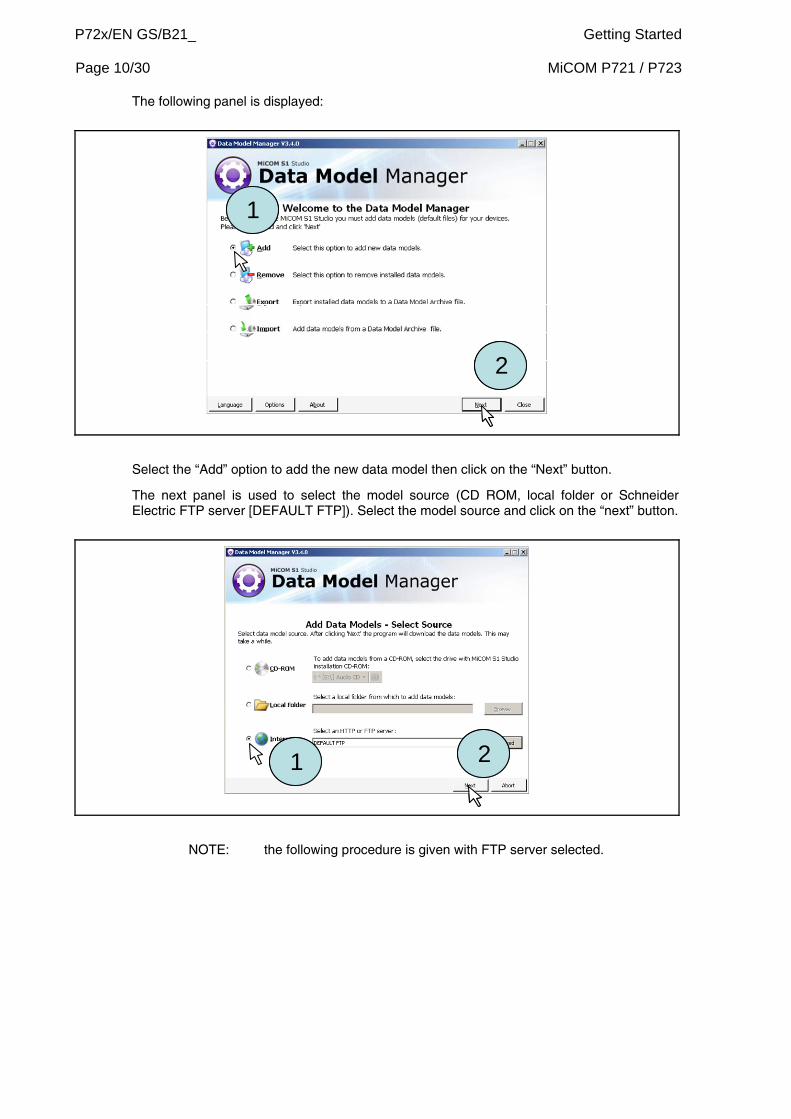
P72x/EN GS/B21_ Getting Started Page 10/30 MiCOM P721 / P723
The following panel is displayed:
1
2
11
22
Select the “Add” option to add the new data model then click on the “Next” button.
The next panel is used to select the model source (CD ROM, local folder or Schneider Electric FTP server [DEFAULT FTP]). Select the model source and click on the “next” button.
21 2211
NOTE: the following procedure is given with FTP server selected.
Getting Started P72x/EN GS/B21_ MiCOM P721 / P723 Page 11/30
The Data Model Manager loads data models details, and then displays automatically the language selection option panel. Select the menu language(s) and click on the “Next” button.
1
2
11
22
The data models panel is displayed. Select the data model for your product (for instance, to download P72x data models, open the “Px10/Px20/Px20C/M/Modulex” sub-menu (click on “+” then select data model according to your product). When data models are selected, the Data Model Manager panel displays the selected models size to download.
1
23
11
2233
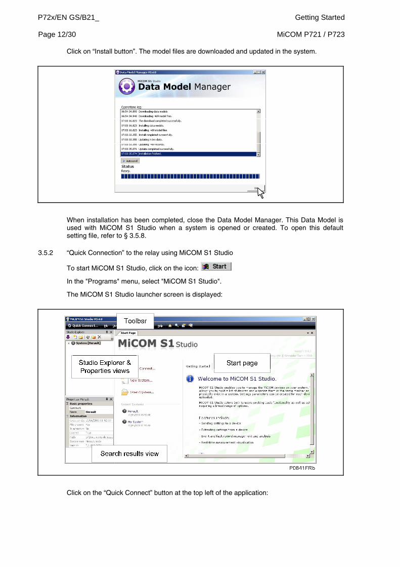
P72x/EN GS/B21_ Getting Started Page 12/30 MiCOM P721 / P723
Click on “Install button”. The model files are downloaded and updated in the system.
When installation has been completed, close the Data Model Manager. This Data Model is used with MiCOM S1 Studio when a system is opened or created. To open this default setting file, refer to § 3.5.8.
3.5.2 “Quick Connection” to the relay using MiCOM S1 Studio
To start MiCOM S1 Studio, click on the icon:
In the "Programs" menu, select "MiCOM S1 Studio".
The MiCOM S1 Studio launcher screen is displayed:
Studio Explorer & Properties views
Start page
Toolbar
Search results view
Studio Explorer & Properties views
Start page
Toolbar
Search results view
Click on the “Quick Connect” button at the top left of the application:

Getting Started P72x/EN GS/B21_ MiCOM P721 / P723 Page 13/30
Create a new system (see § 3.5.3) or open an existing one:
When a system is opened (or created), the following “device type” window is displayed.
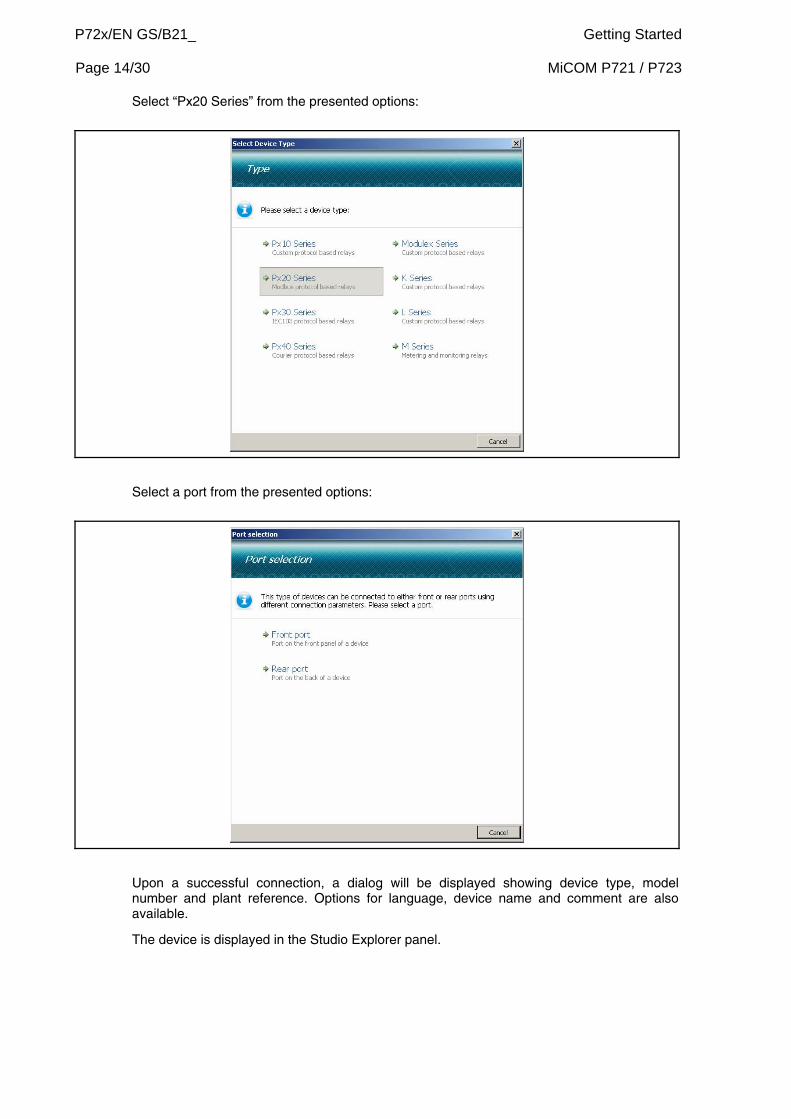
P72x/EN GS/B21_ Getting Started Page 14/30 MiCOM P721 / P723
Select “Px20 Series” from the presented options:
Select a port from the presented options:
Upon a successful connection, a dialog will be displayed showing device type, model number and plant reference. Options for language, device name and comment are also available.
The device is displayed in the Studio Explorer panel.
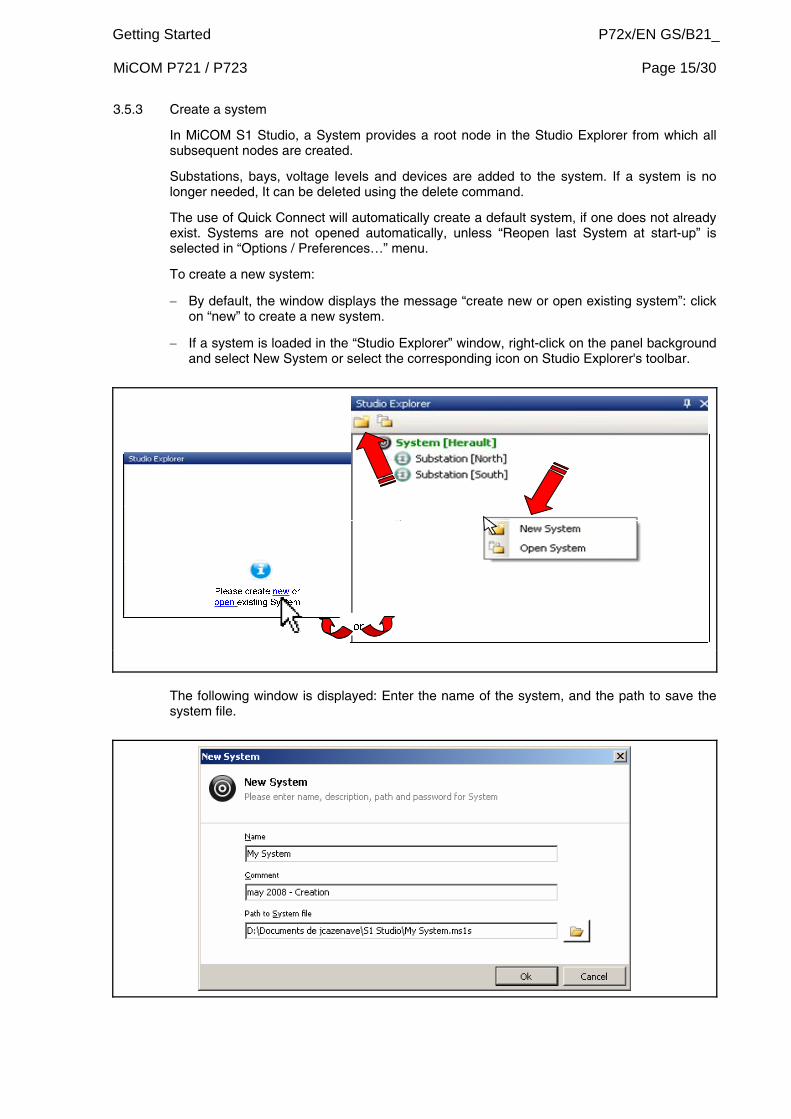
Getting Started P72x/EN GS/B21_ MiCOM P721 / P723 Page 15/30
3.5.3 Create a system
In MiCOM S1 Studio, a System provides a root node in the Studio Explorer from which all subsequent nodes are created.
Substations, bays, voltage levels and devices are added to the system. If a system is no longer needed, It can be deleted using the delete command.
The use of Quick Connect will automatically create a default system, if one does not already exist. Systems are not opened automatically, unless “Reopen last System at start-up” is selected in “Options / Preferences…” menu.
To create a new system:
By default, the window displays the message “create new or open existing system”: click on “new” to create a new system.
If a system is loaded in the “Studio Explorer” window, right-click on the panel background and select New System or select the corresponding icon on Studio Explorer's toolbar.
The following window is displayed: Enter the name of the system, and the path to save the system file.
P72x/EN GS/B21_ Getting Started Page 16/30 MiCOM P721 / P723
The new System is displayed in the Studio Explorer panel:
NOTE: In the Studio Explorer panel, if an item is selected, its properties are displayed in the “Properties” panel
3.5.4 Create a new substation
Select the system: the menu bar is updated with “new device”, “new substation”, “close”, “delete”, “paste”, “properties” and “options” icons.
Create a new device
Create a new substation
Create a new device
Create a new substation
P0901ENa
Click on “new substation” icon (or select the menu using right-click). The following window is displayed:
Getting Started P72x/EN GS/B21_ MiCOM P721 / P723 Page 17/30
The new substation is displayed and the menu bar is updated when a substation is selected:
Create a new voltage level
Import SCL
Create a new voltage level
Import SCL
P0902ENa
Click on “Import SCL” button to import a Substation Configuration File.
To create a substation configuration, click on “new voltage level” button.
3.5.5 Create a new voltage level
Select the substation and click on “new station level” button (or select the menu using right-click).
In the “Create a new voltage level”, enter the voltage level of the station.
The “new voltage level” is displayed and the “new bay” icon is displayed.
Create new bayCreate new bay
P0903ENa
3.5.6 Create a new bay
Select the substation and click on “new bay” button (or select the menu using right-click).
In the “Create new bay…” window, enter the bay indication,
Th new bay is displayed.
P72x/EN GS/B21_ Getting Started Page 18/30 MiCOM P721 / P723 3.5.7 Create a new device
Click on “new device” button (or select the menu using right-click).
Select the device type and, if necessary, the communications protocol mode that will be used to send the file to the device.
12
1122
Select the device type, click “Next” button.
Select the model and click “Next” button.
2
1
3
4
22
11
33
44

Getting Started P72x/EN GS/B21_ MiCOM P721 / P723 Page 19/30
The new device is created and displayed. If necessary, select the MiCOM P72x model using the “OP PARAMETERS/Description” menu.
3.5.8 Open Settings File
To open an existing file:
If the file is saved or if the relay is not connected: open the Settings folder and open the Settings file,
If the relay is connected, extract the settings from the relay: click on the “Extract Settings” command or right click on the Settings folder.
Extract SettingsExtract Settings
P0904ENa
P72x/EN GS/B21_ Getting Started Page 20/30 MiCOM P721 / P723
To open default settings:
Click on “Open Default Settings File” Option in the File menu.
Select the device type then the communication protocol.
Select the device type and click on the “Next” button:
1
2
11
22
Select the Model and click on the “Finish” button. The default settings are displayed.
1
2
1
2
11
22

Getting Started P72x/EN GS/B21_ MiCOM P721 / P723 Page 21/30 3.6 MiCOM S1
3.6.1 Starting MiCOM S1
To start MiCOM S1 Studio, click on the icon: .
In the "Programs" menu, select "MiCOM S1" then "MiCOM S1".
WARNING: CLICKING ON "UNINSTALL MiCOM S1", WILL UNINSTALL MiCOM S1, AND ALL DATA AND RECORDS USED IN MiCOM S1.
You access the MiCOM S1 launcher screen.
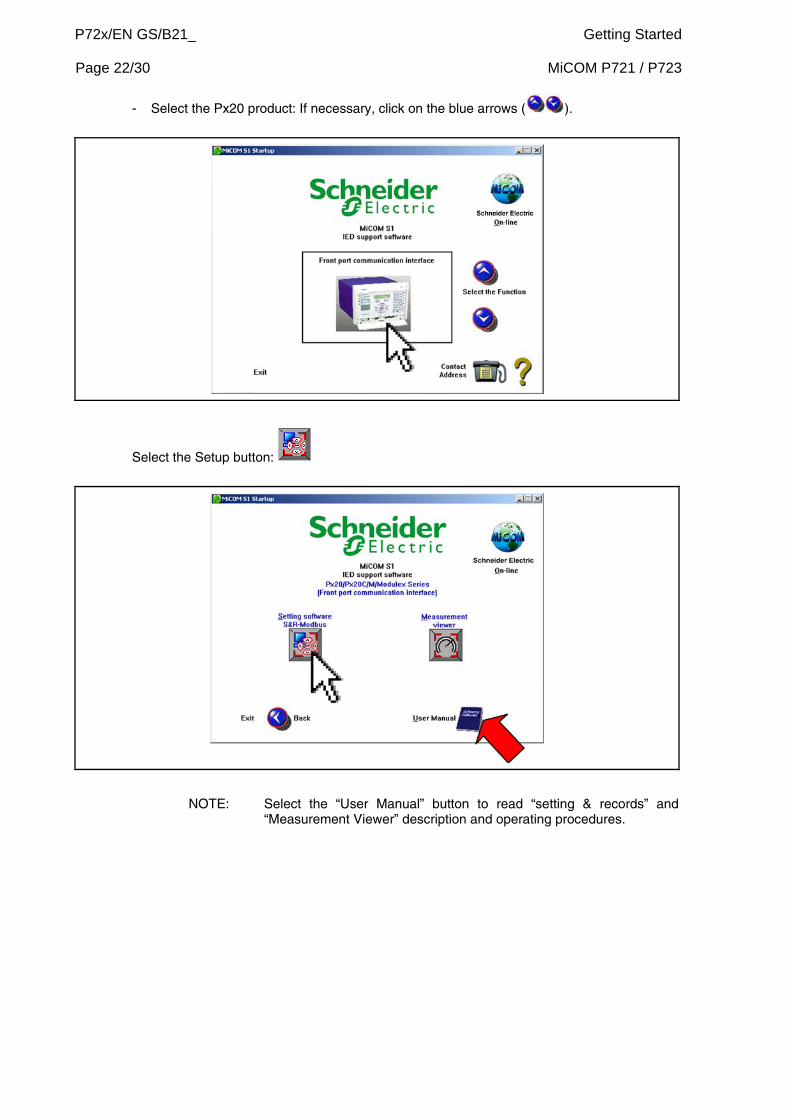
P72x/EN GS/B21_ Getting Started Page 22/30 MiCOM P721 / P723
- Select the Px20 product: If necessary, click on the blue arrows ( ).
Select the Setup button:
NOTE: Select the “User Manual” button to read “setting & records” and “Measurement Viewer” description and operating procedures.

Getting Started P72x/EN GS/B21_ MiCOM P721 / P723 Page 23/30
3.6.2 Open communication link with relay
To open the communications link from S1 to the relay, follow the following procedure.
First, if necessary, the communication setup must be adjusted. In the "Device" menu, select "Communications Setup…"
This brings up the following screen:
COMMUNICATION SET-UP SCREEN
When the communications setup is correct, the link with the relay can be initialized. In the "Device" menu, select "Open Connection…"

P72x/EN GS/B21_ Getting Started Page 24/30 MiCOM P721 / P723
This brings up a prompt for the address of the relay to be interrogated.
When this has been entered, a prompt for the password appears.
When these have been entered satisfactorily the relay is then able to communicate with MiCOM S1. When a communication link has been established between the PC and a MiCOM IED, both are said to be online. Data and information can be directly transferred from and to the IED using the menu available under the “DEVICE” menu.
For further instruction on how to extract, download and modify settings files, please refer to the MiCOM S1 User Manual.
Select the main function in the right hand window.
To modify a setting value, double click the corresponding line in the left hand window. It opens a setting window.
A red star () indicates that a setting value is modified.
1
2
3
11
22
33

Getting Started P72x/EN GS/B21_ MiCOM P721 / P723 Page 25/30 3.6.3 Off-line use of MiCOM S1
As well as being used for the on-line editing of settings, MiCOM S1 can also be used as an off-line tool to prepare settings without access to the relay. In order to open a default setting file for modification, in the “File” menu, select “New” and then “Settings File…”
This brings up a prompt for the relay model type where you can select the correct relay for your application:
Clicking on “OK” will open the default file and you can start to edit settings. For further instruction on how to extract, download and modify settings files, please refer to the MiCOM S1 User Manual.
3.6.4 MiCOM monitoring
The monitoring module enables to connect to the front port, retrieve and monitor its measurements.
Click on the monitoring button: .
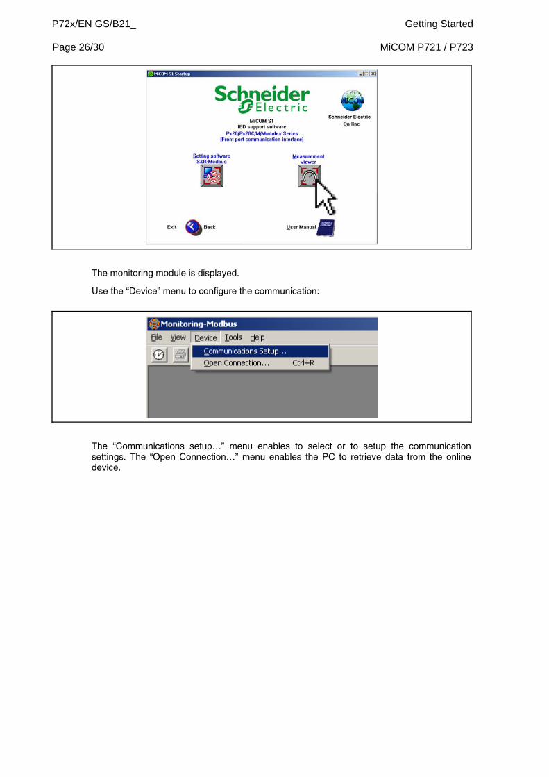
P72x/EN GS/B21_ Getting Started Page 26/30 MiCOM P721 / P723
The monitoring module is displayed.
Use the “Device” menu to configure the communication:
The “Communications setup…” menu enables to select or to setup the communication settings. The “Open Connection…” menu enables the PC to retrieve data from the online device.

Getting Started P72x/EN GS/B21_ MiCOM P721 / P723 Page 27/30 3.7 Presentation and analysis of disturbance
The reading and analysis of disturbance is performed using Wavewin.
To open Wavewin with MiCOM S1:
In the main page, select the function using the blue arrows ( ),
Click on the “presentation and Analysis of Disturbance Recording Data with “Wavewin” window.
Using MiCOM S1 Studio, open Wavewin using “Tools” menu.
The Wavewin File Manager is displayed (refer to the Wavewin User’s guide to operate Wavewin).
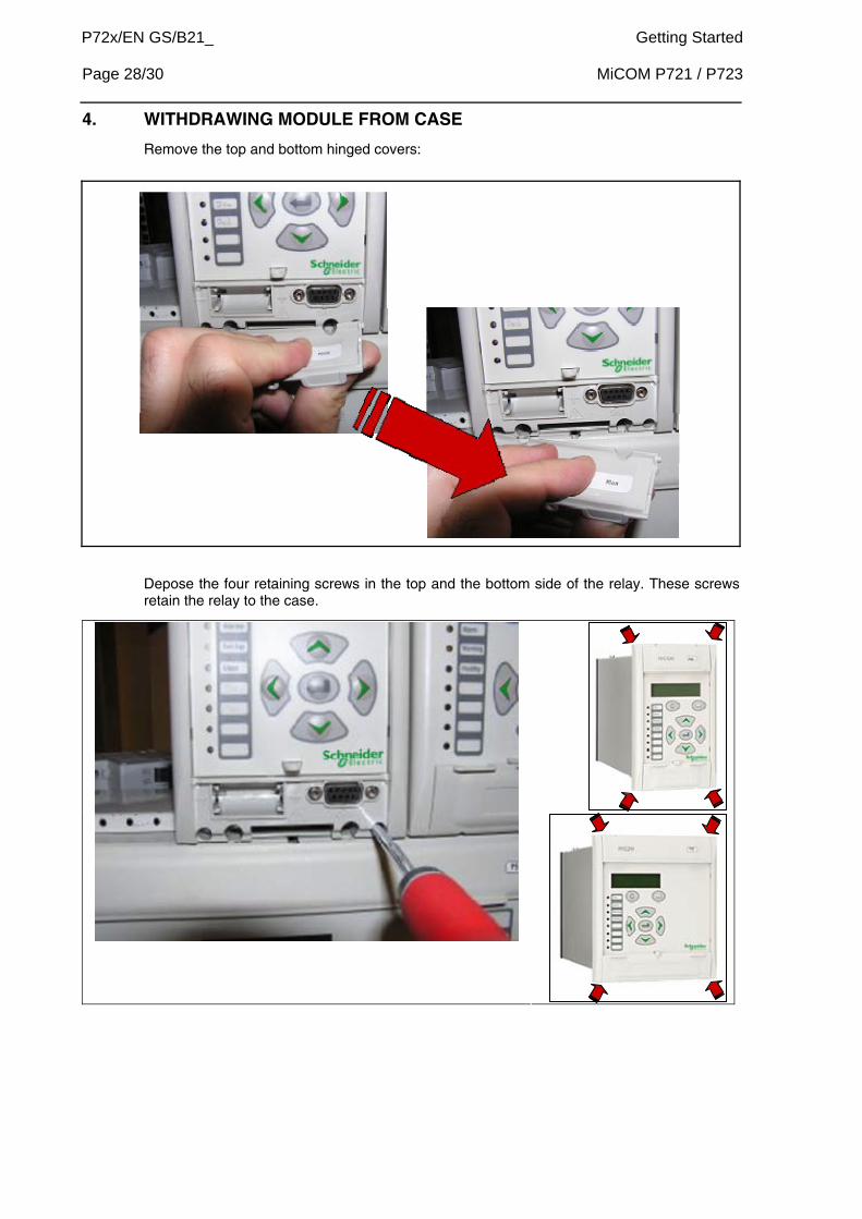
P72x/EN GS/B21_ Getting Started Page 28/30 MiCOM P721 / P723
4. WITHDRAWING MODULE FROM CASE
Remove the top and bottom hinged covers:
Depose the four retaining screws in the top and the bottom side of the relay. These screws retain the relay to the case.

Getting Started P72x/EN GS/B21_ MiCOM P721 / P723 Page 29/30
Insert a 3mm screwdriver into the hole situated under the upper hinged cover above the LCD:
Turn the lock pin 90° to the left:
Insert the screwdriver into the second hole under the lower hinged cover, and the lower lock pin is turned 90° to the right.
By this turning action, push slightly forward the module and extract it by pulling on both sides of the front panel.
P72x/EN GS/B21_ Getting Started Page 30/30 MiCOM P721 / P723
5. COMPANY CONTACT INFORMATION
If you need information pertaining to the operation of this MiCOM product that you have purchased, please contact your local Schneider Electric agent or the Customer Care Center (www.schneider-electric.com/ccc). Do not forget to give the serial number and reference of the MiCOM product.
The MiCOM product reference and serial numbers are documented under the upper hinged cover on the front of the relay. For more precise information, refer to the section "Relay Identification" in this chapter.
PLEASE GIVE THE FOLLOWING DATA WHEN MAKING A CALL TO Schneider Electric:
CORTEC code of the MiCOM relay
Serial number of the MiCOM relay
Order reference
Operator reference

Communication database P72x/EN CT/A11 MiCOM P721/P723
COMMUNICATION DATABASE

P72x /EN CT/A11 Communication database MiCOM P721/P723
BLANK PAGE
Communication database P72x/EN CT/A11 MiCOM P721/P723
MODBUS DATABASE MiCOM P721/P723
VERSION V11

P72x/EN CT/A11 Communication database Page 2/78 MiCOM P721/P723
BLANK PAGE

Communication database P72x/EN CT/A11 MiCOM P721/P723 Page 3/78
CONTENT
1. INTRODUCTION 5
1.1 Purpose of this document 5
2. MODBUS PROTOCOL 6
2.1 Technical characteristics of the MODBUS connection 6 2.1.1 Parameters of the MODBUS connection 6 2.2 Synchronisation of exchanges messages 6 2.3 Message validity check 6 2.4 Address of the MiCOM relays 6 2.5 MODBUS functions of the MiCOM relays 7 2.6 Presentation of the MODBUS protocol 7 2.6.1 Frame size received by the protection device (slave) 7 2.6.2 Format of frames sent by the MiCOM relays 8 2.6.3 Messages validity check 8
3. MiCOM P721 AND P723 RELAY DATABASE ORGANISATION 9
3.1 Description of the application mapping 9 3.1.1 Settings 9 3.2 Page 0h – Product information, remote signalling and measurements 9 3.3 Page 1h – General remote parameters (part 1) 12 3.4 Page 2h –Setting group 1 remote parameters 16 3.5 Page 3h – Setting group 2 remote parameters 17 3.6 Page 4h –Access in writing 17 3.7 Page 5h – Boolean equations remote parameters 18 3.8 Page 6h – General remote parameters (part 2) 22 3.9 Page 7h – Remote device status 22 3.10 Page 8h –Remote data and time 22 3.11 Pages 9h to 21h – Disturbance record data 23 3.11.1 Meaning of each value channel 24 3.11.2 Calculation formula for phase current values 24 3.11.3 Calculation formula for earth current values 24 3.11.4 Logic channels 24 3.12 Page 22h – Disturbance record index frame 24 3.13 Page 35h 25 3.14 Page 36h – Event older record data 27 3.15 Page 37h – Fault record value data 28 3.15.1 Calculation formula for phase current values 28 3.15.2 Calculation formula for earth current values 28 3.16 Page 3Eh – Fault older record data 28

P72x/EN CT/A11 Communication database Page 4/78 MiCOM P721/P723 3.17 Pages 38h to 3Ch – Disturbance record and channel selection 29 3.17.1 Disturbance record and channel selection (13 words) 29 3.17.2 Calculation formula for phase current values 30 3.17.3 Calculation formula for earth current values 30 3.18 Pages 3Dh – Disturbance records number available 30
4. DESCRIPTION OF THE MAPPING FORMAT 32
4.1 Disturbance record additional information 44 4.1.1 MODBUS request definition used for disturbance record 44 4.1.2 Request to know the number of disturbance records in SRAM 44 4.1.3 Service requests 44 4.1.4 Disturbance record upload request 45 4.1.5 Index frame upload request 45 4.1.6 Request to retrieve the oldest non-acknowledge event 45 4.1.7 Request to retrieve a dedicated event 45 4.1.8 Modbus request definition used to retrieve the fault records 46 4.1.9 Request to retrieve the oldest non-acknowledge fault record 46 4.1.10 Request to retrieve a dedicated fault record 46

Communication database P72x/EN CT/A11 MiCOM P721/P723 Page 5/78
1. INTRODUCTION 1.1 Purpose of this document
This document describes the characteristics of the different communication protocol of MiCOM P721 and P723 relays.
The available communication protocols on the relay are listed below:
− MODBUS,
− IEC 60870-5-103,
− DNP3
The K-BUS/Courier is not available with the P72x relays.

P72x/EN CT/A11 Communication database Page 6/78 MiCOM P721/P723
2. MODBUS PROTOCOL MiCOM P721 and P723 relays can communicate by a RS 485 link behind the unit following the MODBUS RTU protocol.
2.1 Technical characteristics of the MODBUS connection
2.1.1 Parameters of the MODBUS connection
The different parameters of the MODBUS connection are as follows:
− Isolated two-point RS485 connection (2kV 50Hz),
− MODBUS line protocol in RTU mode
Communication speed can be configured by an operator dialog in the front panel of the relay:
Baud rate (dec)
300
600
1200
2400
4800
9600
19200
38400
Transmission mode of the configured characters by operator dialog
Mode
1 start / 8 bits / 1 stop: total 10 bits
1 start / 8 bits / even parity / 1 stop: total 11 bits
1 start / 8 bits / odd parity / 1 stop: total 11 bits
1 start / 8 bits / 2 stop: total 11 bits
2.2 Synchronisation of exchanges messages
A character received after a silence (≥ 3 characters transmission time) is considered as a frame start.
2.3 Message validity check
The validation of a frame is performed with a 16-bit Cyclical Redundancy Check (CRC). Generator polynomial: 1+x²+x15+x16 = 1010 0000 0000 0001 (binary) = A001 (hexadecimal)
2.4 Address of the MiCOM relays
The address of the MiCOM relay on a same MODBUS network is situated between 1 and 255. The address 0 is reserved for the broadcast messages

Communication database P72x/EN CT/A11 MiCOM P721/P723 Page 7/78 2.5 MODBUS functions of the MiCOM relays
Protection device data may be read or modified by using function codes. Following are the available function codes. Function codes to read from or write into parameter cells in the protection device are described in the listed following table.
Function Nr. Data Read Data Write Data Format & Type
1 X N bits
2 X N bits
3 X N words
4 X N words
5 X 1 bit
6 X 1 word
7 Fast 8 bits
8 X Diagnostics counter
11 X Event counter
15 X N bits
16 X N words
2.6 Presentation of the MODBUS protocol
Master slave protocol, all exchange understands a master query and a slave response
Frame size received from MiCOM P721 and P723 relays.
2.6.1 Frame size received by the protection device (slave)
Frame transmitted by the master ( query):
Slave number Function code Information CRC16
1 byte 1 byte n bytes 2 bytes
0 à FFh 1 à 10h
Slave number:
The slave number is situated between 1 and 255.
A frame transmitted with a slave number 0 is globally addressed to all pieces of equipment (broadcast frame)
Error code:
The MiCOM P72x relays manages the two following error codes:
• Code 01: the function code is not authorised or is unknown.
• Code 03: one of the following value from the data field is incorrect:
− control of data being read, − control of data being written, − control of data address, − length of request for data message.
CRC16:
Value of the CRC16 calculated by the master.
NOTE: The MiCOM relay does not respond to globally broadcast frames sent out by the master.

P72x/EN CT/A11 Communication database Page 8/78 MiCOM P721/P723 2.6.2 Format of frames sent by the MiCOM relays
Frame sent by the MiCOM relay (response)
Slave number Function code Data CRC16
1 byte 1 byte n bytes 2 bytes
1 à FFh 1 à 10h
Slave number:
The slave number is situated between 1 and 255.
Function code:
Processed MODBUS function (1 to 16).
Data:
Contains reply data to master query .
CRC 16:
Value of the CRC 16 calculated by the slave.
2.6.3 Messages validity check
When MiCOM P721 and P723 relays receive a master query, it validates the frame:
− If the CRC is false, the frame is invalid. MiCOM 721 and P723 relays do not reply to the query. The master must retransmit its query. Excepting a broadcast message, this is the only case of non-reply by MiCOM P721 and P723 relays to a master query.
− If the CRC is good but the MiCOM relay can not process the query, it sends an exception response.
Warning frame sent by the MiCOM relay (response)
Slave number Function code Warning code CRC16
1 byte 1 byte 1 byte 2 bytes
1 to FFh 81h or 83h or 8Ah or 8Bh pf ... PF
Slave number:
The slave number is situated between 1 and 255.
Function code:
The function code returned by the MiCOM relay in the warning frame is the code in which the most significant bit (b7) is forced to 1.
Warning code:
On the 8 warning codes of the MODBUS protocol, the MiCOM relay manages two of them:
• code 01: function code unauthorised or unknown.
• code 03: a value in the data field is unauthorised ( incorrect data ).
− Control of pages being read − Control of pages being written − Control of addresses in pages − Length of request messages
CRC16:
Value of the CRC16 calculated by the slave.
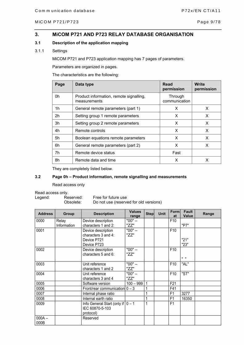
Communication database P72x/EN CT/A11 MiCOM P721/P723 Page 9/78
3. MiCOM P721 AND P723 RELAY DATABASE ORGANISATION 3.1 Description of the application mapping
3.1.1 Settings
MiCOM P721 and P723 application mapping has 7 pages of parameters.
Parameters are organized in pages.
The characteristics are the following:
Page Data type Read permission
Write permission
0h Product information, remote signalling, measurements
Through communication
1h General remote parameters (part 1) X X
2h Setting group 1 remote parameters X X
3h Setting group 2 remote parameters X X
4h Remote controls X X
5h Boolean equations remote parameters X X
6h General remote parameters (part 2) X X
7h Remote device status Fast
8h Remote data and time X X
They are completely listed below.
3.2 Page 0h – Product information, remote signalling and measurements
Read access only
Read access only. Legend: Reserved: Free for future use Obsolete: Do not use (reserved for old versions)
Address Group Description Values range Step Unit Form
at Fault Value Range
0000 Relay Information
Device description characters 1 and 2:
"00" – "ZZ"
F10 "P7"
0001 Device description characters 3 and 4: Device P721 Device P723
"00" – "ZZ"
F10 "21" "23"
0002 Device description characters 5 and 6:
"00" – "ZZ"
F10 " "
0003 Unit reference characters 1 and 2
"00" – "ZZ"
F10 "AL"
0004 Unit reference characters 3 and 4
"00" – "ZZ"
F10 "ST"
0005 Software version 100 – 999 1 F21 0006 Front/rear communication 0 – 3 1 F41 0007 Internal phase ratio 1 F1 3277 0008 Internal earth ratio 1 F1 16350 0009 Info General Start (only if
IEC 60870-5-103 protocol)
0 – 1 1 F1
000A – 000B
Reserved

P72x/EN CT/A11 Communication database Page 10/78 MiCOM P721/P723
Address Group Description Values range Step Unit Form
at Fault Value Range
000C LED Status Binary 1 F73 8h (healthy)
000D Real Active Setting Group (after taking into account the protection flags)
1 – 2 1 F51
000E Password active ? 0 – 1 1 F24 0 (no) 000F Material alarm status Binary 1 F45 0 (no
warning)
0010 Remote signalling
Logical inputs status Binary 1 F12 0 (no input)
0011 Logic output relay status Binary 1 F13 10h (WD)
0012– 0013
logical inputs data signalisation
Binary 1 F20
0014 Trip status 0 – 3 1 F22 0 0015– 0016
Reserved
0017 Information of [87] CZ status
Binary 1 F17 0
0018 Information of [95] SUP status
Binary 1 F17 0
0019 Information of [87] DIFF status
Binary 1 F17 0
001A Information of [95N] SUP status
Binary 1 F16 0
001B Information of [87N] DIFF status
Binary 1 F16 0
001C–001D
Information of general instantaneous status
Binary 1 F38 0
001E Information of equation status
Binary 1 F61 0
001F Reserved 0020 Alarms
memorised Memorisation of [95] SUP non acknowledged alarms
Binary 1 F17 0
0021 Memorisation of [87] DIFF non acknowledged alarms
Binary 1 F17 0
0022 Reserved 0023 Memorisation of [95]
tSUP non acknowledged alarms
Binary 1 F17 0
0024 Memorisation of [87] tDIFF non acknowledged alarms
Binary 1 F17 0
0025 Reserved 0026– 0028
Memorised flag for non acknowledged alarms
Binary 1 F36 0
0029 Number of disturbance records available
0 – 5 1 F1 0
002A Tripping origin 0 – 26 1 F78 0 002B Memorised logic output
relay latched Binary 1 F13 0
002C–002E
Reserved

Communication database P72x/EN CT/A11 MiCOM P721/P723 Page 11/78
Address Group Description Values range Step Unit Form
at Fault Value Range
002F measure-ments
Frequency 4500 – 6500 9999 if out
1 10 mHz F1 9999
0030–0031 Phase A RMS value 0 – 600 000
1 10 mA F18 0
0032–0033 Phase B RMS value 0 – 600 000
1 10 mA F18 0
0034–0035 Phase C RMS value 0 – 600 000
1 10 mA F18 0
0036 – 0037
Earth RMS value 0 – 120 000
1 10 mA F18 0
0038 – 0039
Phase A maximum RMS value
0 – 600 000
1 10 mA F18 0
003A – 003B
Phase B maximum RMS value
0 – 600 000
1 10 mA F18 0
003C–003D
Phase C maximum RMS value
0 – 600 000
1 10 mA F18 0
003E – 003F
Earth maximum RMS value
0 – 120 000
1 10 mA F18 0
0040– 004F
Reserved
0050 Amplitudes for sample protection
Phase A Amplitude value of TC secondary (CAN format)
In / Add. 0007h
F1
0051 Phase B Amplitude value of TC secondary (CAN format)
In / Add. 0007h
F1
0052 Phase C Amplitude value of TC secondary (CAN format)
In / Add. 0007h
F1
0053 Earth Amplitude value of TC secondary (CAN format)
In / Add. 0008h
F1
0054 Amplitudes for fast sample protection
Phase A Amplitude value of TC secondary (CAN format)
In / Add. 0007h
F1
0055 Phase B Amplitude value of TC secondary (CAN format)
In / Add. 0007h
F1
0056 Phase C Amplitude value of TC secondary (CAN format)
In / Add. 0007h
F1
0057 Earth Amplitude value of TC secondary (CAN format)
In / Add. 0008h
F1
0058 Amplitudes for Fourier protection
Phase A Amplitude value of TC secondary (CAN format)
In / Add. 0007h
F1
0059 Phase B Amplitude value of TC secondary (CAN format)
In / Add. 0007h
F1
005A Phase C Amplitude value of TC secondary (CAN format)
In / Add. 0007h
F1
005B Earth Amplitude value of TC secondary (CAN format)
In / Add. 0008h
F1
005C– 00DF
Reserved
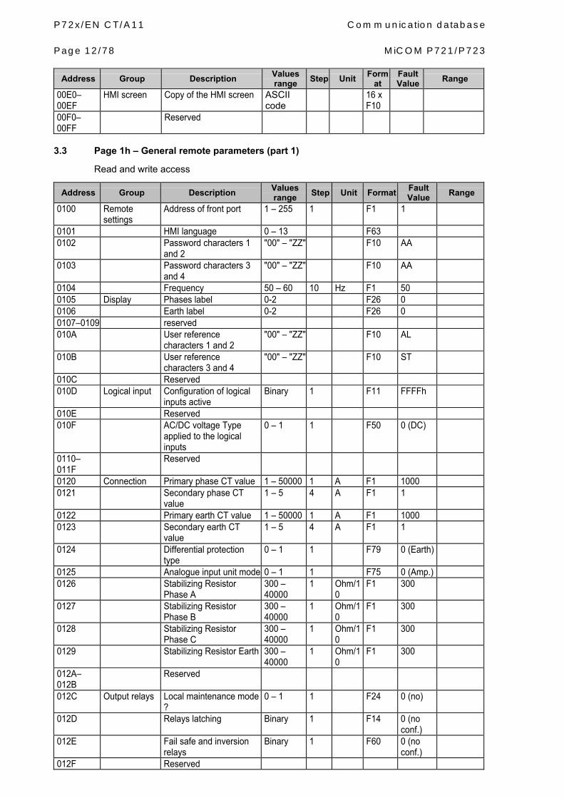
P72x/EN CT/A11 Communication database Page 12/78 MiCOM P721/P723
Address Group Description Values range Step Unit Form
at Fault Value Range
00E0– 00EF
HMI screen Copy of the HMI screen ASCII code
16 x F10
00F0– 00FF
Reserved
3.3 Page 1h – General remote parameters (part 1)
Read and write access
Address Group Description Values range Step Unit Format Fault
Value Range
0100 Remote settings
Address of front port 1 – 255 1 F1 1
0101 HMI language 0 – 13 F63 0102 Password characters 1
and 2 "00" – "ZZ" F10 AA
0103 Password characters 3 and 4
"00" – "ZZ" F10 AA
0104 Frequency 50 – 60 10 Hz F1 50 0105 Display Phases label 0-2 F26 0 0106 Earth label 0-2 F26 0 0107–0109 reserved 010A User reference
characters 1 and 2 "00" – "ZZ" F10 AL
010B User reference characters 3 and 4
"00" – "ZZ" F10 ST
010C Reserved 010D Logical input Configuration of logical
inputs active Binary 1 F11 FFFFh
010E Reserved 010F AC/DC voltage Type
applied to the logical inputs
0 – 1 1 F50 0 (DC)
0110– 011F
Reserved
0120 Connection Primary phase CT value 1 – 50000 1 A F1 1000 0121 Secondary phase CT
value 1 – 5 4 A F1 1
0122 Primary earth CT value 1 – 50000 1 A F1 1000 0123 Secondary earth CT
value 1 – 5 4 A F1 1
0124 Differential protection type
0 – 1 1 F79 0 (Earth)
0125 Analogue input unit mode 0 – 1 1 F75 0 (Amp.) 0126 Stabilizing Resistor
Phase A 300 – 40000
1 Ohm/10
F1 300
0127 Stabilizing Resistor Phase B
300 – 40000
1 Ohm/10
F1 300
0128 Stabilizing Resistor Phase C
300 – 40000
1 Ohm/10
F1 300
0129 Stabilizing Resistor Earth 300 – 40000
1 Ohm/10
F1 300
012A– 012B
Reserved
012C Output relays Local maintenance mode ?
0 – 1 1 F24 0 (no)
012D Relays latching Binary 1 F14 0 (no conf.)
012E Fail safe and inversion relays
Binary 1 F60 0 (no conf.)
012F Reserved
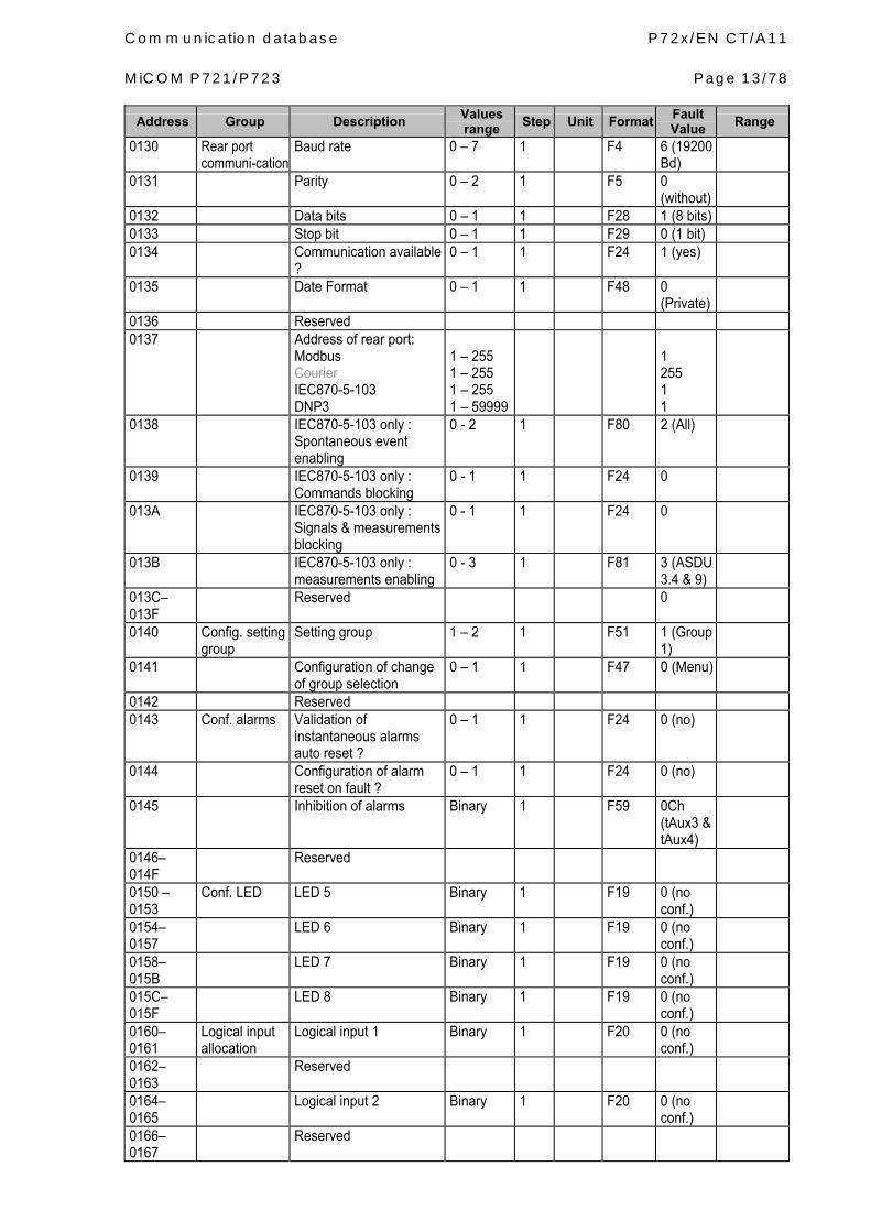
Communication database P72x/EN CT/A11 MiCOM P721/P723 Page 13/78
Address Group Description Values range Step Unit Format Fault
Value Range
0130 Rear port communi-cation
Baud rate 0 – 7 1 F4 6 (19200 Bd)
0131 Parity 0 – 2 1 F5 0 (without)
0132 Data bits 0 – 1 1 F28 1 (8 bits) 0133 Stop bit 0 – 1 1 F29 0 (1 bit) 0134 Communication available
? 0 – 1 1 F24 1 (yes)
0135 Date Format 0 – 1 1 F48 0 (Private)
0136 Reserved 0137 Address of rear port:
Modbus Courier IEC870-5-103 DNP3
1 – 255 1 – 255 1 – 255 1 – 59999
1 255 1 1
0138 IEC870-5-103 only : Spontaneous event enabling
0 - 2 1 F80 2 (All)
0139 IEC870-5-103 only : Commands blocking
0 - 1 1 F24 0
013A IEC870-5-103 only : Signals & measurements blocking
0 - 1 1 F24 0
013B IEC870-5-103 only : measurements enabling
0 - 3 1 F81 3 (ASDU 3.4 & 9)
013C– 013F
Reserved 0
0140 Config. setting group
Setting group 1 – 2 1 F51 1 (Group 1)
0141 Configuration of change of group selection
0 – 1 1 F47 0 (Menu)
0142 Reserved 0143 Conf. alarms Validation of
instantaneous alarms auto reset ?
0 – 1 1 F24 0 (no)
0144 Configuration of alarm reset on fault ?
0 – 1 1 F24 0 (no)
0145 Inhibition of alarms Binary 1 F59 0Ch (tAux3 & tAux4)
0146– 014F
Reserved
0150 – 0153
Conf. LED LED 5 Binary 1 F19 0 (no conf.)
0154– 0157
LED 6 Binary 1 F19 0 (no conf.)
0158– 015B
LED 7 Binary 1 F19 0 (no conf.)
015C– 015F
LED 8 Binary 1 F19 0 (no conf.)
0160– 0161
Logical input allocation
Logical input 1 Binary 1 F20 0 (no conf.)
0162– 0163
Reserved
0164– 0165
Logical input 2 Binary 1 F20 0 (no conf.)
0166– 0167
Reserved

P72x/EN CT/A11 Communication database Page 14/78 MiCOM P721/P723
Address Group Description Values range Step Unit Format Fault
Value Range
0168– 0169
Logical input 3 Binary 1 F20 0 (no conf.)
016A– 016B
Reserved
016C– 016D
Logical input 4 Binary 1 F20 0 (no conf.)
016 – 016F
Reserved
0170– 0171
Logical input 5 Binary 1 F20 0 (no conf.)
0172 – 0173
reserved
0174 – 017B
reserved
017C Auxiliary input 1 timer 0 – 20000 1 10 ms F1 0 017D Auxiliary input 2 timer 0 – 20000 1 10 ms F1 0 017E Auxiliary input 3 timer 0 – 20000 1 10 ms F1 0 017F Auxiliary input 4 timer 0 – 20000 1 10 ms F1 0 0180 Output relay
allocation Trip Binary 1 F14 0 (no
conf.)
0181 [87] DIFF Binary 1 F14 0 (no conf.)
0182 [87] tDIFF Binary 1 F14 0 (no conf.)
0183 [87CZ] check zone Binary 1 F14 0 (no conf.)
0184 Buswire shorting Binary 1 F14 0 (no conf.)
0185 reserved 0186 [95] SUP Binary 1 F14 0 (no
conf.)
0187 [95] tSUP Binary 1 F14 0 (no conf.)
0188 [95A] tSUP Binary 1 F14 0 (no conf.)
0189 [95B] tSUP Binary 1 F14 0 (no conf.)
018A [95C] tSUP Binary 1 F14 0 (no conf.)
018B– 018D
reserved
018E [87N] DIFF Binary 1 F14 0 (no conf.)
018F [87N] tDIFF Binary 1 F14 0 (no conf.)
0190 [95N] SUP Binary 1 F14 0 (no conf.)
0191 [95N] tSUP Binary 1 F14 0 (no conf.)
0192– 0193
reserved
0194 tAux 1 Binary 1 F14 0 (no conf.)
0195 tAux 2 Binary 1 F14 0 (no conf.)
0196 tAux 3 Binary 1 F14 0 (no conf.)
0197 tAux 4 Binary 1 F14 0 (no conf.)

Communication database P72x/EN CT/A11 MiCOM P721/P723 Page 15/78
Address Group Description Values range Step Unit Format Fault
Value Range
0198 tEquation A Binary 1 F14 0 (no conf.)
0199 tEquation B Binary 1 F14 0 (no conf.)
019A tEquation C Binary 1 F14 0 (no conf.)
019B tEquation D Binary 1 F14 0 (no conf.)
019C tEquation E Binary 1 F14 0 (no conf.)
019D tEquation F Binary 1 F14 0 (no conf.)
019E tEquation G Binary 1 F14 0 (no conf.)
019F tEquation H Binary 1 F14 0 (no conf.)
01A0 Logical input 1 (energized)
Binary 1 F14 0 (no conf.)
01A1 Logical input 2 (energized)
Binary 1 F14 0 (no conf.)
01A2 Logical input 3 (energized)
Binary 1 F14 0 (no conf.)
01A3 Logical input 4 (energized)
Binary 1 F14 0 (no conf.)
01A4 Logical input 5 (energized)
Binary 1 F14 0 (no conf.)
01A5–01A6
Reserved
01A7 CB failure (50BF) Binary 1 F14 0 (no conf.)
01A8 Active setting group 2 Binary 1 F14 0 (no conf.)
01A9 Control trip (from communication)
Binary 1 F14 0 (no conf.)
01AA– 01AD
Reserved
01AE Automatism Reserved 01AF CB Operating time 10 – 500 1 10 ms F1 10 01B0– 01B1
Trip command Binary 1 F6 0 (no conf.)
01B2– 01B3
Trip function latching Binary 1 F6 0 (no conf.)
01B4– 01B5
Blocking logic Blocking logic 1 Binary 1 F8 0 (no conf.)
01B6– 01B7
Blocking logic 2 Binary 1 F8 0 (no conf.)
01B8– 01BF
Reserved
01C0 Default record Default number to be displayed
1 – 25 1 F1 25 (newest)
01C1 Instantaneous fault number to be displayed
1 – 5 1 F1 5 (newest)
01C2– 01C4
Reserved
01C5 Disturbance record
Pre-time 10 – 300 1 10 ms F1 100
01C6 Post-time 10 – 300 1 10 ms F1 200 01C7 Disturbance starting
condition 0 – 1 1 F32 0 (inst.)

P72x/EN CT/A11 Communication database Page 16/78 MiCOM P721/P723
Address Group Description Values range Step Unit Format Fault
Value Range
01C8–01CF
Reserved
01D0 CB failure [50BF]
CB failure function ? 0 - 1 1 F24 0 (no)
01D1 Idiff< CB failure 1 – 100 1 In/100 F1 10 01D2 tBF 3 – 1000 1 10 ms F1 10 01D3 Vdiff< CB failure 5 – 2000 10 100
mV F1 50
01D4–01DF
Reserved
01E0 Equation timer Equation A rising tempo 0 – 60000 1 10 ms F1 0 01E1 Equation A falling tempo 0 – 60000 1 10 ms F1 0 01E2 Equation B rising tempo 0 – 60000 1 10 ms F1 0 01E3 Equation B falling tempo 0 – 60000 1 10 ms F1 0 01E4 Equation C rising tempo 0 – 60000 1 10 ms F1 0 01E5 Equation C falling tempo 0 – 60000 1 10 ms F1 0 01E6 Equation D rising tempo 0 – 60000 1 10 ms F1 0 01E7 Equation D falling tempo 0 – 60000 1 10 ms F1 0 01E8 Equation E rising tempo 0 – 60000 1 10 ms F1 0 01E9 Equation E falling tempo 0 – 60000 1 10 ms F1 0 01EA Equation F rising tempo 0 – 60000 1 10 ms F1 0 01EB Equation F falling tempo 0 – 60000 1 10 ms F1 0 01EC Equation G rising tempo 0 – 60000 1 10 ms F1 0 01ED Equation G falling tempo 0 – 60000 1 10 ms F1 0 01EE Equation H rising tempo 0 – 60000 1 10 ms F1 0 01EF Equation H falling tempo 0 – 60000 1 10 ms F1 0 01F0 – 01FF
Reserved
3.4 Page 2h –Setting group 1 remote parameters
Access in reading and in writing Address Group Description Values
range Step Unit Format Fault Value Range
0200 [87] ph. differential
[87] DIFF function ? 0 – 1 1 F24 0 (No)
0201 [87] Current IDIFF Threshold
2 – 200 1 In/100 F1 200
0202 [87] Voltage VDIFF Threshold
10 – 4000 10 100 mV F1 4000
0203 [87] tDIFF timer value 0 – 200 1 10 ms F1 0 0204 [87] tRESET timer value 0 – 60000 1 10 ms F1 0 0205 [87] Filter of analog input
protection 1, 3, 4 1 F74 1
(Sample mode)
0206 [87] Check zone permission ?
0 – 1 1 F24 0 (No)
0207– 021F
Reserved
0220 [95] Buswire supervision
[95] SUP function ? 0 – 1 1 F24 0 (No)
0221 [95] Current ISUP Threshold
2– 200 1 In/100 F1 200
0222 [95] Voltage VSUP Threshold
10 – 4000 10 100 mV F1 4000
0223 [95] tSUP timer value 50 – 300 1 10 ms F1 300 0224 [95] tRESET timer value 0 – 60000 1 10 ms F1 0
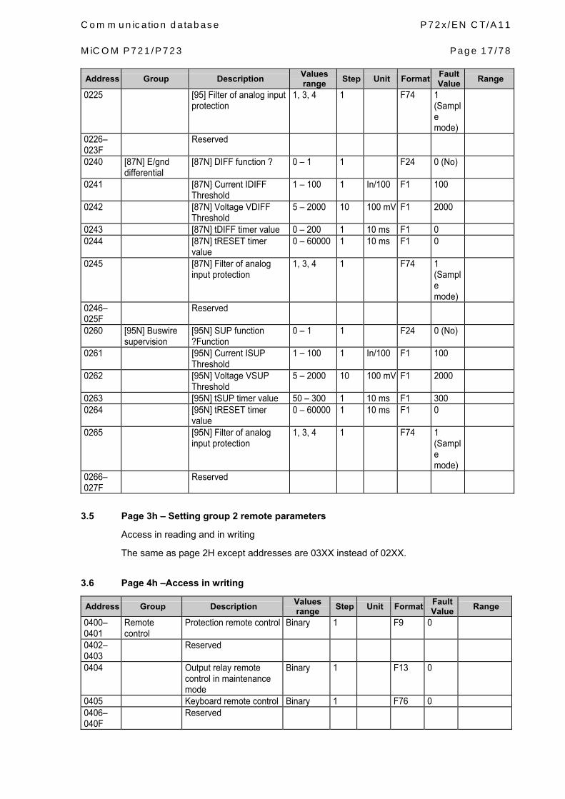
Communication database P72x/EN CT/A11 MiCOM P721/P723 Page 17/78
Address Group Description Values range Step Unit Format Fault
Value Range
0225 [95] Filter of analog input protection
1, 3, 4 1 F74 1 (Sample mode)
0226– 023F
Reserved
0240 [87N] E/gnd differential
[87N] DIFF function ? 0 – 1 1 F24 0 (No)
0241 [87N] Current IDIFF Threshold
1 – 100 1 In/100 F1 100
0242 [87N] Voltage VDIFF Threshold
5 – 2000 10 100 mV F1 2000
0243 [87N] tDIFF timer value 0 – 200 1 10 ms F1 0 0244 [87N] tRESET timer
value 0 – 60000 1 10 ms F1 0
0245 [87N] Filter of analog input protection
1, 3, 4 1 F74 1 (Sample mode)
0246– 025F
Reserved
0260 [95N] Buswire supervision
[95N] SUP function ?Function
0 – 1 1 F24 0 (No)
0261 [95N] Current ISUP Threshold
1 – 100 1 In/100 F1 100
0262 [95N] Voltage VSUP Threshold
5 – 2000 10 100 mV F1 2000
0263 [95N] tSUP timer value 50 – 300 1 10 ms F1 300 0264 [95N] tRESET timer
value 0 – 60000 1 10 ms F1 0
0265 [95N] Filter of analog input protection
1, 3, 4 1 F74 1 (Sample mode)
0266– 027F
Reserved
3.5 Page 3h – Setting group 2 remote parameters
Access in reading and in writing
The same as page 2H except addresses are 03XX instead of 02XX.
3.6 Page 4h –Access in writing
Address Group Description Values range Step Unit Format Fault
Value Range
0400–0401
Remote control
Protection remote control Binary 1 F9 0
0402–0403
Reserved
0404 Output relay remote control in maintenance mode
Binary 1 F13 0
0405 Keyboard remote control Binary 1 F76 0 0406–040F
Reserved

P72x/EN CT/A11 Communication database Page 18/78 MiCOM P721/P723
3.7 Page 5h – Boolean equations remote parameters
Read and write access.
Address (hex) Group Description Values range Step Unit Format Def.
Value0500 Bool Equations Equation A.00 operator 0 – 1 1 F70 0 0501 Equation A.00 operand 0 – 24 1 F72 0 0502 Equation A.01 operator 0 – 3 1 F71 0 0503 Equation A.01 operand 0 – 24 1 F72 0 0504 Equation A.02 operator 0 – 3 1 F71 0 0505 Equation A.02 operand 0 – 24 1 F72 0 0506 Equation A.03 operator 0 – 3 1 F71 0 0507 Equation A.03 operand 0 – 24 1 F72 0 0508 Equation A.04 operator 0 – 3 1 F71 0 0509 Equation A.04 operand 0 – 24 1 F72 0 050A Equation A.05 operator 0 – 3 1 F71 0 050B Equation A.05 operand 0 – 24 1 F72 0 050C Equation A.06 operator 0 – 3 1 F71 0 050D Equation A.06 operand 0 – 24 1 F72 0 050E Equation A.07 operator 0 – 3 1 F71 0 050F Equation A.07 operand 0 – 24 1 F72 0 0510 Equation A.08 operator 0 – 3 1 F71 0 0511 Equation A.08 operand 0 – 24 1 F72 0 0512 Equation A.09 operator 0 – 3 1 F71 0 0513 Equation A.09 operand 0 – 24 1 F72 0 0514 Equation A.10 operator 0 – 3 1 F71 0 0515 Equation A.10 operand 0 – 24 1 F72 0 0516 Equation A.11 operator 0 – 3 1 F71 0 0517 Equation A.11 operand 0 – 24 1 F72 0 0518 Equation A.12 operator 0 – 3 1 F71 0 0519 Equation A.12 operand 0 – 24 1 F72 0 051A Equation A.13 operator 0 – 3 1 F71 0 051B Equation A.13 operand 0 – 24 1 F72 0 051C Equation A.14 operator 0 – 3 1 F71 0 051D Equation A.14 operand 0 – 24 1 F72 0 051E Equation A.15 operator 0 – 3 1 F71 0 051F Equation A.15 operand 0 – 24 1 F72 0 0520 Equation B.00 operator 0 – 1 1 F70 0 0521 Equation B.00 operand 0 – 24 1 F72 0 0522 Equation B.01 operator 0 – 3 1 F71 0 0523 Equation B.01 operand 0 – 24 1 F72 0 0524 Equation B.02 operator 0 – 3 1 F71 0 0525 Equation B.02 operand 0 – 24 1 F72 0 0526 Equation B.03 operator 0 – 3 1 F71 0 0527 Equation B.03 operand 0 – 24 1 F72 0 0528 Equation B.04 operator 0 – 3 1 F71 0 0529 Equation B.04 operand 0 – 24 1 F72 0 052A Equation B.05 operator 0 – 3 1 F71 0 052B Equation B.05 operand 0 – 24 1 F72 0 052C Equation B.06 operator 0 – 3 1 F71 0 052D Equation B.06 operand 0 – 24 1 F72 0 052E Equation B.07 operator 0 – 3 1 F71 0 052F Equation B.07 operand 0 – 24 1 F72 0 0530 Equation B.08 operator 0 – 3 1 F71 0 0531 Equation B.08 operand 0 – 24 1 F72 0 0532 Equation B.09 operator 0 – 3 1 F71 0 0533 Equation B.09 operand 0 – 24 1 F72 0 0534 Equation B.10 operator 0 – 3 1 F71 0 0535 Equation B.10 operand 0 – 24 1 F72 0 0536 Equation B.11 operator 0 – 3 1 F71 0
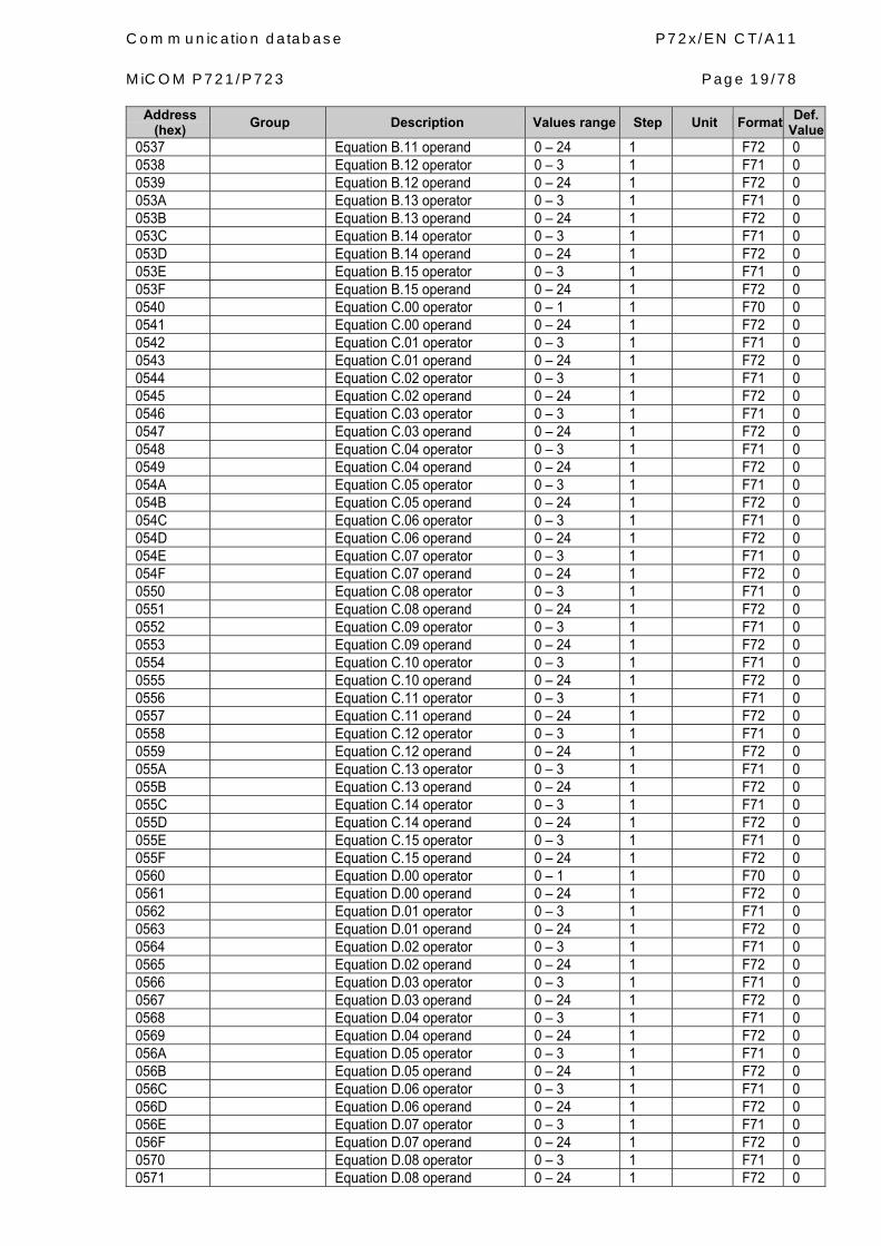
Communication database P72x/EN CT/A11 MiCOM P721/P723 Page 19/78
Address (hex) Group Description Values range Step Unit Format Def.
Value0537 Equation B.11 operand 0 – 24 1 F72 0 0538 Equation B.12 operator 0 – 3 1 F71 0 0539 Equation B.12 operand 0 – 24 1 F72 0 053A Equation B.13 operator 0 – 3 1 F71 0 053B Equation B.13 operand 0 – 24 1 F72 0 053C Equation B.14 operator 0 – 3 1 F71 0 053D Equation B.14 operand 0 – 24 1 F72 0 053E Equation B.15 operator 0 – 3 1 F71 0 053F Equation B.15 operand 0 – 24 1 F72 0 0540 Equation C.00 operator 0 – 1 1 F70 0 0541 Equation C.00 operand 0 – 24 1 F72 0 0542 Equation C.01 operator 0 – 3 1 F71 0 0543 Equation C.01 operand 0 – 24 1 F72 0 0544 Equation C.02 operator 0 – 3 1 F71 0 0545 Equation C.02 operand 0 – 24 1 F72 0 0546 Equation C.03 operator 0 – 3 1 F71 0 0547 Equation C.03 operand 0 – 24 1 F72 0 0548 Equation C.04 operator 0 – 3 1 F71 0 0549 Equation C.04 operand 0 – 24 1 F72 0 054A Equation C.05 operator 0 – 3 1 F71 0 054B Equation C.05 operand 0 – 24 1 F72 0 054C Equation C.06 operator 0 – 3 1 F71 0 054D Equation C.06 operand 0 – 24 1 F72 0 054E Equation C.07 operator 0 – 3 1 F71 0 054F Equation C.07 operand 0 – 24 1 F72 0 0550 Equation C.08 operator 0 – 3 1 F71 0 0551 Equation C.08 operand 0 – 24 1 F72 0 0552 Equation C.09 operator 0 – 3 1 F71 0 0553 Equation C.09 operand 0 – 24 1 F72 0 0554 Equation C.10 operator 0 – 3 1 F71 0 0555 Equation C.10 operand 0 – 24 1 F72 0 0556 Equation C.11 operator 0 – 3 1 F71 0 0557 Equation C.11 operand 0 – 24 1 F72 0 0558 Equation C.12 operator 0 – 3 1 F71 0 0559 Equation C.12 operand 0 – 24 1 F72 0 055A Equation C.13 operator 0 – 3 1 F71 0 055B Equation C.13 operand 0 – 24 1 F72 0 055C Equation C.14 operator 0 – 3 1 F71 0 055D Equation C.14 operand 0 – 24 1 F72 0 055E Equation C.15 operator 0 – 3 1 F71 0 055F Equation C.15 operand 0 – 24 1 F72 0 0560 Equation D.00 operator 0 – 1 1 F70 0 0561 Equation D.00 operand 0 – 24 1 F72 0 0562 Equation D.01 operator 0 – 3 1 F71 0 0563 Equation D.01 operand 0 – 24 1 F72 0 0564 Equation D.02 operator 0 – 3 1 F71 0 0565 Equation D.02 operand 0 – 24 1 F72 0 0566 Equation D.03 operator 0 – 3 1 F71 0 0567 Equation D.03 operand 0 – 24 1 F72 0 0568 Equation D.04 operator 0 – 3 1 F71 0 0569 Equation D.04 operand 0 – 24 1 F72 0 056A Equation D.05 operator 0 – 3 1 F71 0 056B Equation D.05 operand 0 – 24 1 F72 0 056C Equation D.06 operator 0 – 3 1 F71 0 056D Equation D.06 operand 0 – 24 1 F72 0 056E Equation D.07 operator 0 – 3 1 F71 0 056F Equation D.07 operand 0 – 24 1 F72 0 0570 Equation D.08 operator 0 – 3 1 F71 0 0571 Equation D.08 operand 0 – 24 1 F72 0

P72x/EN CT/A11 Communication database Page 20/78 MiCOM P721/P723
Address (hex) Group Description Values range Step Unit Format Def.
Value0572 Equation D.09 operator 0 – 3 1 F71 0 0573 Equation D.09 operand 0 – 24 1 F72 0 0574 Equation D.10 operator 0 – 3 1 F71 0 0575 Equation D.10 operand 0 – 24 1 F72 0 0576 Equation D.11 operator 0 – 3 1 F71 0 0577 Equation D.11 operand 0 – 24 1 F72 0 0578 Equation D.12 operator 0 – 3 1 F71 0 0579 Equation D.12 operand 0 – 24 1 F72 0 057A Equation D.13 operator 0 – 3 1 F71 0 057B Equation D.13 operand 0 – 24 1 F72 0 057C Equation D.14 operator 0 – 3 1 F71 0 057D Equation D.14 operand 0 – 24 1 F72 0 057E Equation D.15 operator 0 – 3 1 F71 0 057F Equation D.15 operand 0 – 24 1 F72 0 0580 Equation E.00 operator 0 – 1 1 F70 0 0581 Equation E.00 operand 0 – 24 1 F72 0 0582 Equation E.01 operator 0 – 3 1 F71 0 0583 Equation E.01 operand 0 – 24 1 F72 0 0584 Equation E.02 operator 0 – 3 1 F71 0 0585 Equation E.02 operand 0 – 24 1 F72 0 0586 Equation E.03 operator 0 – 3 1 F71 0 0587 Equation E.03 operand 0 – 24 1 F72 0 0588 Equation E.04 operator 0 – 3 1 F71 0 0589 Equation E.04 operand 0 – 24 1 F72 0 058A Equation E.05 operator 0 – 3 1 F71 0 058B Equation E.05 operand 0 – 24 1 F72 0 058C Equation E.06 operator 0 – 3 1 F71 0 058D Equation E.06 operand 0 – 24 1 F72 0 058E Equation E.07 operator 0 – 3 1 F71 0 058F Equation E.07 operand 0 – 24 1 F72 0 0590 Equation E.08 operator 0 – 3 1 F71 0 0591 Equation E.08 operand 0 – 24 1 F72 0 0592 Equation E.09 operator 0 – 3 1 F71 0 0593 Equation E.09 operand 0 – 24 1 F72 0 0594 Equation E.10 operator 0 – 3 1 F71 0 0595 Equation E.10 operand 0 – 24 1 F72 0 0596 Equation E.11 operator 0 – 3 1 F71 0 0597 Equation E.11 operand 0 – 24 1 F72 0 0598 Equation E.12 operator 0 – 3 1 F71 0 0599 Equation E.12 operand 0 – 24 1 F72 0 059A Equation E.13 operator 0 – 3 1 F71 0 059B Equation E.13 operand 0 – 24 1 F72 0 059C Equation E.14 operator 0 – 3 1 F71 0 059D Equation E.14 operand 0 – 24 1 F72 0 059E Equation E.15 operator 0 – 3 1 F71 0 059F Equation E.15 operand 0 – 24 1 F72 0 05A0 Equation F.00 operator 0 – 1 1 F70 0 05A1 Equation F.00 operand 0 – 24 1 F72 0 05A2 Equation F.01 operator 0 – 3 1 F71 0 05A3 Equation F.01 operand 0 – 24 1 F72 0 05A4 Equation F.02 operator 0 – 3 1 F71 0 05A5 Equation F.02 operand 0 – 24 1 F72 0 05A6 Equation F.03 operator 0 – 3 1 F71 0 05A7 Equation F.03 operand 0 – 24 1 F72 0 05A8 Equation F.04 operator 0 – 3 1 F71 0 05A9 Equation F.04 operand 0 – 24 1 F72 0 05AA Equation F.05 operator 0 – 3 1 F71 0 05AB Equation F.05 operand 0 – 24 1 F72 0 05AC Equation F.06 operator 0 – 3 1 F71 0

Communication database P72x/EN CT/A11 MiCOM P721/P723 Page 21/78
Address (hex) Group Description Values range Step Unit Format Def.
Value05AD Equation F.06 operand 0 – 24 1 F72 0 05AE Equation F.07 operator 0 – 3 1 F71 0 05AF Equation F.07 operand 0 – 24 1 F72 0 05B0 Equation F.08 operator 0 – 3 1 F71 0 05B1 Equation F.08 operand 0 – 24 1 F72 0 05B2 Equation F.09 operator 0 – 3 1 F71 0 05B3 Equation F.09 operand 0 – 24 1 F72 0 05B4 Equation F.10 operator 0 – 3 1 F71 0 05B5 Equation F.10 operand 0 – 24 1 F72 0 05B6 Equation F.11 operator 0 – 3 1 F71 0 05B7 Equation F.11 operand 0 – 24 1 F72 0 05B8 Equation F.12 operator 0 – 3 1 F71 0 05B9 Equation F.12 operand 0 – 24 1 F72 0 05BA Equation F.13 operator 0 – 3 1 F71 0 05BB Equation F.13 operand 0 – 24 1 F72 0 05BC Equation F.14 operator 0 – 3 1 F71 0 05BD Equation F.14 operand 0 – 24 1 F72 0 05BE Equation F.15 operator 0 – 3 1 F71 0 05BF Equation F.15 operand 0 – 24 1 F72 0 05C0 Equation G.00 operator 0 – 1 1 F70 0 05C1 Equation G.00 operand 0 – 24 1 F72 0 05C2 Equation G.01 operator 0 – 3 1 F71 0 05C3 Equation G.01 operand 0 – 24 1 F72 0 05C4 Equation G.02 operator 0 – 3 1 F71 0 05C5 Equation G.02 operand 0 – 24 1 F72 0 05C6 Equation G.03 operator 0 – 3 1 F71 0 05C7 Equation G.03 operand 0 – 24 1 F72 0 05C8 Equation G.04 operator 0 – 3 1 F71 0 05C9 Equation G.04 operand 0 – 24 1 F72 0 05CA Equation G.05 operator 0 – 3 1 F71 0 05CB Equation G.05 operand 0 – 24 1 F72 0 05CC Equation G.06 operator 0 – 3 1 F71 0 05CD Equation G.06 operand 0 – 24 1 F72 0 05CE Equation G.07 operator 0 – 3 1 F71 0 05CF Equation G.07 operand 0 – 24 1 F72 0 05D0 Equation G.08 operator 0 – 3 1 F71 0 05D1 Equation G.08 operand 0 – 24 1 F72 0 05D2 Equation G.09 operator 0 – 3 1 F71 0 05D3 Equation G.09 operand 0 – 24 1 F72 0 05D4 Equation G.10 operator 0 – 3 1 F71 0 05D5 Equation G.10 operand 0 – 24 1 F72 0 05D6 Equation G.11 operator 0 – 3 1 F71 0 05D7 Equation G.11 operand 0 – 24 1 F72 0 05D8 Equation G.12 operator 0 – 3 1 F71 0 05D9 Equation G.12 operand 0 – 24 1 F72 0 05DA Equation G.13 operator 0 – 3 1 F71 0 05DB Equation G.13 operand 0 – 24 1 F72 0 05DC Equation G.14 operator 0 – 3 1 F71 0 05DD Equation G.14 operand 0 – 24 1 F72 0 05DE Equation G.15 operator 0 – 3 1 F71 0 05DF Equation G.15 operand 0 – 24 1 F72 0 05E0 Equation H.00 operator 0 – 1 1 F70 0 05E1 Equation H.00 operand 0 – 24 1 F72 0 05E2 Equation H.01 operator 0 – 3 1 F71 0 05E3 Equation H.01 operand 0 – 24 1 F72 0 05E4 Equation H.02 operator 0 – 3 1 F71 0 05E5 Equation H.02 operand 0 – 24 1 F72 0 05E6 Equation H.03 operator 0 – 3 1 F71 0 05E7 Equation H.03 operand 0 – 24 1 F72 0

P72x/EN CT/A11 Communication database Page 22/78 MiCOM P721/P723
Address (hex) Group Description Values range Step Unit Format Def.
Value05E8 Equation H.04 operator 0 – 3 1 F71 0 05E9 Equation H.04 operand 0 – 24 1 F72 0 05EA Equation H.05 operator 0 – 3 1 F71 0 05EB Equation H.05 operand 0 – 24 1 F72 0 05EC Equation H.06 operator 0 – 3 1 F71 0 05ED Equation H.06 operand 0 – 24 1 F72 0 05EE Equation H.07 operator 0 – 3 1 F71 0 05EF Equation H.07 operand 0 – 24 1 F72 0 05F0 Equation H.08 operator 0 – 3 1 F71 0 05F1 Equation H.08 operand 0 – 24 1 F72 0 05F2 Equation H.09 operator 0 – 3 1 F71 0 05F3 Equation H.09 operand 0 – 24 1 F72 0 05F4 Equation H.10 operator 0 – 3 1 F71 0 05F5 Equation H.10 operand 0 – 24 1 F72 0 05F6 Equation H.11 operator 0 – 3 1 F71 0 05F7 Equation H.11 operand 0 – 24 1 F72 0 05F8 Equation H.12 operator 0 – 3 1 F71 0 05F9 Equation H.12 operand 0 – 24 1 F72 0 05FA Equation H.13 operator 0 – 3 1 F71 0 05FB Equation H.13 operand 0 – 24 1 F72 0 05FC Equation H.14 operator 0 – 3 1 F71 0 05FD Equation H.14 operand 0 – 24 1 F72 0 05FE Equation H.15 operator 0 – 3 1 F71 0 05FF Equation H.15 operand 0 – 24 1 F72 0
3.8 Page 6h – General remote parameters (part 2)
Read and write access
Address Group Description Values range Step Unit Format Fault
Value0600 – 06FF
Reserved
3.9 Page 7h – Remote device status
Access in quick reading only (MODBUS 07 function)
Address Group Description Values range Step Unit Format Fault
Value0700 Device status 1 - F23 1
3.10 Page 8h –Remote data and time
Read and write access
Time synchronisation: access in writing for n words (function 16). The time synchronisation format is based on 8 bits (4 words).
If date Format (0135h) is private date then format is:
Address Group Description Values range Step Unit Format Fault
Value0800 Date Year 1994-2093 1 Year F1 1994 0801 Month 1 -12 1 Month F1
MSB 1
Day 1 – 31 1 Days F1 lsb
1
0802 Hour 0 – 23 1 Hours F1 MSB
0
Minute 0 – 59 1 mn F1 lsb
0
0803 Milliseconds 0 – 59999 1 ms F1 0
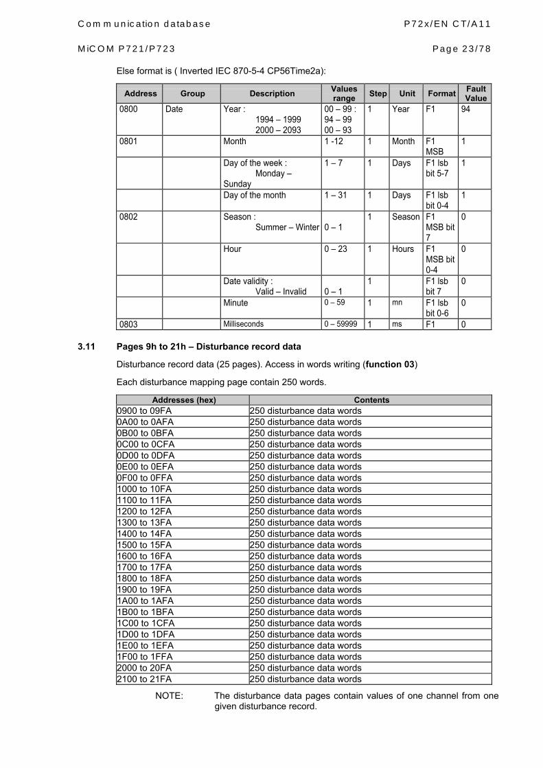
Communication database P72x/EN CT/A11 MiCOM P721/P723 Page 23/78
Else format is ( Inverted IEC 870-5-4 CP56Time2a):
Address Group Description Values range Step Unit Format Fault
Value0800 Date Year :
1994 – 1999 2000 – 2093
00 – 99 : 94 – 99 00 – 93
1 Year F1 94
0801 Month 1 -12 1 Month F1 MSB
1
Day of the week : Monday – Sunday
1 – 7 1 Days F1 lsb bit 5-7
1
Day of the month 1 – 31 1 Days F1 lsb bit 0-4
1
0802 Season : Summer – Winter
0 – 1
1 Season F1 MSB bit 7
0
Hour 0 – 23 1 Hours F1 MSB bit 0-4
0
Date validity : Valid – Invalid
0 – 1
1 F1 lsb bit 7
0
Minute 0 – 59 1 mn F1 lsb bit 0-6
0
0803 Milliseconds 0 – 59999 1 ms F1 0
3.11 Pages 9h to 21h – Disturbance record data
Disturbance record data (25 pages). Access in words writing (function 03)
Each disturbance mapping page contain 250 words.
Addresses (hex) Contents 0900 to 09FA 250 disturbance data words 0A00 to 0AFA 250 disturbance data words 0B00 to 0BFA 250 disturbance data words 0C00 to 0CFA 250 disturbance data words 0D00 to 0DFA 250 disturbance data words 0E00 to 0EFA 250 disturbance data words 0F00 to 0FFA 250 disturbance data words 1000 to 10FA 250 disturbance data words 1100 to 11FA 250 disturbance data words 1200 to 12FA 250 disturbance data words 1300 to 13FA 250 disturbance data words 1400 to 14FA 250 disturbance data words 1500 to 15FA 250 disturbance data words 1600 to 16FA 250 disturbance data words 1700 to 17FA 250 disturbance data words 1800 to 18FA 250 disturbance data words 1900 to 19FA 250 disturbance data words 1A00 to 1AFA 250 disturbance data words 1B00 to 1BFA 250 disturbance data words 1C00 to 1CFA 250 disturbance data words 1D00 to 1DFA 250 disturbance data words 1E00 to 1EFA 250 disturbance data words 1F00 to 1FFA 250 disturbance data words 2000 to 20FA 250 disturbance data words 2100 to 21FA 250 disturbance data words
NOTE: The disturbance data pages contain values of one channel from one given disturbance record.

P72x/EN CT/A11 Communication database Page 24/78 MiCOM P721/P723 3.11.1 Meaning of each value channel
• IA, IB, IC and IO channels:
The value is an signed 16 bits word equivalent to the ADC value
3.11.2 Calculation formula for phase current values
Line phase current value (primary value) = phase sampled value x phase primary CT / phase internal CT ratio (mapping address 0007 = 800) x √2
3.11.3 Calculation formula for earth current values
Line earth current value (primary value) = earth sampled value (e.g. word 10 or 14) x earth primary CT / earth internal CT ratio (mapping address 0008h) x √2
3.11.4 Logic channels
Logic channel MODBUS & DNP 3.0 IEC 61870-5-103 Bit 0 Trip relay (RL1) Earth Starting Bit 1 Output relay 2 General Starting Bit 2 Output relay 3 CB Fail Bit 3 Output relay 4 General Trip Bit 4 Watch-dog relay [95] tSUP Bit 5 Output relay 5 [87] tDIFF Bit 6 Output relay 6 Reserved Bit 7 Output relay 7 [95N] tSUP Bit 8 Output relay 8 [87N] tDIFF Bit 9 Reserved Reserved Bit 10 Logic input 1 Logic input 1 Bit 11 Logic input 2 Logic input 2 Bit 12 Logic input 3 Logic input 3 Bit 13 Logic input 4 Logic input 4 Bit 14 Logic input 5 Logic input 5 Bit 15 Reserved Reserved
3.12 Page 22h – Disturbance record index frame
Disturbance record index frame (7 to 9 Words)
Access in word reading (function 03)
Addresses Contents 2200h Disturbance data index frame
Disturbance record index frame
Word Contents n° 1 Disturbance record number n° 2 Disturbance record finish date (second) n° 3 Disturbance record finish date (second) n° 4 Disturbance record finish date (millisecond) n° 5 Disturbance record finish date (millisecond) n° 6 Disturbance record starting condition:
1: tripping command (RL1) 2: instantaneous 3: remote command 4: logic input
n° 7 Frequency at the post-time beginning n° 8 (=0) Optional n° 9 (=0) Optional

Communication database P72x/EN CT/A11 MiCOM P721/P723 Page 25/78
3.13 Page 35h
Addresses 3500h to 354Ah.
Addresses (hex) Contents
3500 Event records 1
3501 Event records 2
… …
354A Event records 250
Event record data (9 words)
Word n° 1: Event code
Word n° 2: MODBUS associated value
Word n° 3: MODBUS address
Word n° 4:
Words n° 5 & 6 if data format is private:
Event date (second) number of seconds since 01/01/94
Words n° 7 & 8 if data format is private:
Event date (millisecond)
Words N°5, 6, 7, 8, if data format is Inverted IEC 870-5-4 CP56Time2a:
See format page 8h
Word n° 9: Acknowledge 0=event non acknowledged 1= event acknowledged
Code Meaning of the event Type MODBUS address
COURIER Cell
00 No event 01 02 Remote control tripping F9 Ctrl 1 03 Disturbance recording start F82 04 Trip output unlatched F9 Ctrl 1 05 Setting change Address 06 07 Maintenance Mode F45 ↑ ↓ Yes 08 Output relay remote word in
maintenance mode F13
09 [95] SUP F17 ↑ ↓ Yes 10 [87] DIFF F17 ↑ ↓ Yes 11 12 [95N] SUP F16 ↑ ↓ Yes 13 [87N] DIFF F16 ↑ ↓ Yes 14 15 16 17 [95] tSUP F17 ↑ ↓ Yes 18 [87] tDIFF F17 ↑ ↓ Yes 19 20 [95N] tSUP F16 ↑ ↓ Yes 21 [87N] tDIFF F16 ↑ ↓ Yes

P72x/EN CT/A11 Communication database Page 26/78 MiCOM P721/P723
Code Meaning of the event Type MODBUS address
COURIER Cell
22 23 24 25 tAux 1 F38 word 1↑ ↓ Yes 26 tAux 2 F38 word 1 ↑ ↓ Yes 27 CB Failure (50BF) F38 word 1 ↑ ↓ Yes 28 29 30 Blocking logic 1 F20 word 1 ↑ ↓ Yes 31 Blocking logic 2 F20 word 1 ↑ ↓ Yes 32 Setting group change 1 or 2 33 34 35 Output relays unlatched (Logical
input) F20 word 1 ↑ ↓
36 37 38 Change of logical input state F12 ↑ ↓ 39 40 41 [87] tDIFF fault (tripping) F13 42 43 44 [87N] tDIFF fault (tripping) F13 45 46 47 48 tAux 1 fault (tripping) F13 49 tAux 2 fault (tripping) F13 50 Output relays command F13 51 Front panel single alarm
acknowledge.
52 Front panel all alarms acknowledge 53 Remote single alarm acknowledge 54 Remote all alarms acknowledge 55 Major material alarm F45 ↑ ↓ Yes 56 Minor material alarm F45 ↑ ↓ Yes 57 58 59 60 61 62 63 64 65 66 67 68 General Start (IEC 60870-5-103) F24 ↑ ↓ 69 70 71 Auxiliary output relays latched F13 Yes 72 73 74 75 76 77 Local Mode (IEC 60870-5-103) F24 ↑ ↓

Communication database P72x/EN CT/A11 MiCOM P721/P723 Page 27/78
Code Meaning of the event Type MODBUS address
COURIER Cell
78 Trip output relay latched F22 ↑ ↓ 79 tAux 3 F38 word 1 ↑ ↓ Yes 80 tAux 3 fault (tripping) F13 81 tAux 4 F38 word 1 ↑ ↓ Yes 82 tAux 4 fault (tripping) F13 83 84 85 86 87 88 89 90 91 92 93 Local Mode F20 word 2 ↑ ↓ 94 Reset alarms & LED (IEC 60870-5-
103)
95 96 97 Synchronization > 10 s F23 98 99 tEquation A F61 ↑ ↓ Yes 100 tEquation B F61 ↑ ↓ Yes 101 tEquation C F61 ↑ ↓ Yes 102 tEquation D F61 ↑ ↓ Yes 103 tEquation E F61 ↑ ↓ Yes 104 tEquation F F61 ↑ ↓ Yes 105 tEquation G F61 ↑ ↓ Yes 106 tEquation H F61 ↑ ↓ Yes 107 tEquation A fault (tripping) F13 108 tEquation B fault (tripping) F13 109 tEquation C fault (tripping) F13 110 tEquation D fault (tripping) F13 111 tEquation E fault (tripping) F13 112 tEquation F fault (tripping) F13 113 tEquation G fault (tripping) F13 114 tEquation H fault (tripping) F13 115 t[87CZ] check zone F17 ↑ ↓ Yes 116 Buswire shorting F36 word 1 ↑ ↓ Yes 117 Signals & measurements blocking
(IEC 60870-5-103) F24 ↑ ↓
118 Commands blocking (IEC 60870-5-103) F24 ↑ ↓
NOTA: The double arrow ↑ ↓ means the event is generated on event occurrence (↑) and on event disappearance (↓). On event occurrence, the corresponding bit of the associated format is set to « 1 ». On event disappearance, the corresponding bit of the associated format is set to « 0 ».
3.14 Page 36h – Event older record data
Access in word reading (function 03)
Addresses Contents 3600h Most older event data

P72x/EN CT/A11 Communication database Page 28/78 MiCOM P721/P723 3.15 Page 37h – Fault record value data
Access in word reading (function 03)
Addresses Contents 3700h Fault value record n°1 3701h Fault value record n°2 3702h Fault value record n°3 … … 3718h Fault value record n°25
Each record is made up of 15 words:
Word Nr. Contents 1 Fault number PRIVATE FORMAT: 2 & 3 Fault date (number of seconds since 01/01/94) PRIVATE FORMAT: 4 & 5 Fault date (milli-seconds) IEC FORMAT: 2 to 5 Fault date (see format of time synchronisation, address 0800h) 6 Fault date (season)
0= winter 1= summer 2= undefined
7 Active setting group during the fault (1 or 2) 8 Phase/earth fault origin (format F77) 9 Fault recording starting origin (format F78) 10 Fault value 11 Phase A current value (nominal value) 12 Phase B current value (nominal value) 13 Phase C current value (nominal value) 14 Earth current value (nominal value) 15 Acknowledgement:
0 = fault not acknowledged 1 = fault acknowledged
3.15.1 Calculation formula for phase current values
Line phase current value (primary value) = phase sampled value (e.g. word 10, 11, 12 or 13) x phase primary CT / phase internal CT ratio (mapping address 0007 = 800)
3.15.2 Calculation formula for earth current values
Line earth current value (primary value) = earth sampled value (e.g. word 10 or 14) * earth primary CT ratio / earth internal CT ratio (mapping address 0008h).
3.16 Page 3Eh – Fault older record data
Access in word reading (function 03)
Addresses Contents 3E00h Most older Fault record

Communication database P72x/EN CT/A11 MiCOM P721/P723 Page 29/78
3.17 Pages 38h to 3Ch – Disturbance record and channel selection
Selection of the disturbance record and channel (11 to 13 words are uploaded for each address reading)
Access in word reading (function 03)
Address Disturbance record number Format 3800h 1 IA 3801h 1 IB 3802h 1 IC 3803h 1 IE 3804h 1 Frequency 3805h 1 Logic input and outputs 3900h 2 IA 3901h 2 IB 3902h 2 IC 3903h 2 IE 3904h 2 Frequency 3905h 2 Logic input and outputs 3A00h 3 IA 3A01h 3 IB 3A02h 3 IC 3A03h 3 IE 3A04h 3 Frequency 3A05h 3 Logic input and outputs 3B00h 4 IA 3B01h 4 IB 3B02h 4 IC 3B03h 4 IE 3B04h 4 Frequency 3B05h 4 Logic input and outputs 3C00h 5 IA 3C01h 5 IB 3C02h 5 IC 3C03h 5 IE 3C04h 5 Frequency 3C05h 5 Logic input and outputs
3.17.1 Disturbance record and channel selection (13 words)
Word n° 1: Number of samples included in the mapping
Word n° 2: Sample number in pre-time
Word n° 3: Sample number in post-time
Word n° 4: Phase primary CT ratio
Word n° 5: Phase secondary CT ratio
Word n° 6: Earth primary CT ratio
Word n° 7: Earth secondary CT ratio
Word n° 8: Phase internal CT ratio
Word n° 9: Earth internal CT ratio
Word n° 10: Mapping last page number
Word n° 11: Number of words in the mapping last page
Word n° 12: Coefficient of samples conversion (=1) (Optional)
Word n° 13: Reference of samples conversion (=1) (Optional)
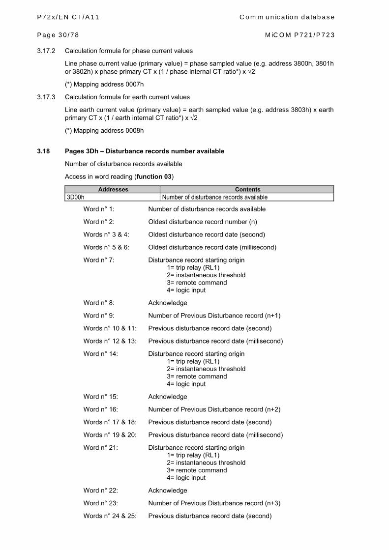
P72x/EN CT/A11 Communication database Page 30/78 MiCOM P721/P723 3.17.2 Calculation formula for phase current values
Line phase current value (primary value) = phase sampled value (e.g. address 3800h, 3801h or 3802h) x phase primary CT x (1 / phase internal CT ratio*) x √2
(*) Mapping address 0007h
3.17.3 Calculation formula for earth current values
Line earth current value (primary value) = earth sampled value (e.g. address 3803h) x earth primary CT x (1 / earth internal CT ratio*) x √2
(*) Mapping address 0008h
3.18 Pages 3Dh – Disturbance records number available
Number of disturbance records available
Access in word reading (function 03)
Addresses Contents 3D00h Number of disturbance records available
Word n° 1: Number of disturbance records available
Word n° 2: Oldest disturbance record number (n)
Words n° 3 & 4: Oldest disturbance record date (second)
Words n° 5 & 6: Oldest disturbance record date (millisecond)
Word n° 7: Disturbance record starting origin 1= trip relay (RL1) 2= instantaneous threshold 3= remote command 4= logic input
Word n° 8: Acknowledge
Word n° 9: Number of Previous Disturbance record (n+1)
Words n° 10 & 11: Previous disturbance record date (second)
Words n° 12 & 13: Previous disturbance record date (millisecond)
Word n° 14: Disturbance record starting origin 1= trip relay (RL1) 2= instantaneous threshold 3= remote command 4= logic input
Word n° 15: Acknowledge
Word n° 16: Number of Previous Disturbance record (n+2)
Words n° 17 & 18: Previous disturbance record date (second)
Words n° 19 & 20: Previous disturbance record date (millisecond)
Word n° 21: Disturbance record starting origin 1= trip relay (RL1) 2= instantaneous threshold 3= remote command 4= logic input
Word n° 22: Acknowledge
Word n° 23: Number of Previous Disturbance record (n+3)
Words n° 24 & 25: Previous disturbance record date (second)

Communication database P72x/EN CT/A11 MiCOM P721/P723 Page 31/78
Words n° 26 & 27: Previous disturbance record date (millisecond)
Word n° 28: Disturbance record starting origin 1= trip relay (RL1) 2= instantaneous threshold 3= remote command 4= logic input
Word n° 29: Acknowledge
Word n° 30: Number of Previous Disturbance record (n+4)
Words n° 31 & 32: Previous disturbance record date (second)
Words n° 33 & 34: Previous disturbance record date (millisecond)
Word n° 35: Disturbance record starting origin 1= trip relay (RL1) 2= instantaneous threshold 3= remote command 4= logic input
Word n° 36: Acknowledge

P72x/EN CT/A11 Communication database Page 32/78 MiCOM P721/P723
4. DESCRIPTION OF THE MAPPING FORMAT CODE DESCRIPTION
F1 Unsigned integer – numerical data: 0 to 65535 F2 Signed integer – numerical data: -32768 to 32767 F3 Reserved F4 Unsigned integer: MODBUS speed
0: 300 bd 1: 600 bd 2: 1200 bd 3: 2400 bd 4: 4800 bd 5: 9600 bd 6: 19200 bd 7: 38400 bd
F5 Unsigned integer: parity 0: without 1: even 2: odd
F6 Unsigned integer: Tripping configuration and latching Word 1: bit 0: bit 1: [87] tDIFF bit 2: bit 3: bit 4: [87N] tDIFF bit 5: bit 6: bit 7: bit 8: bit 9: tAux 1 bit 10: tAux 2 bit 11: bit 12: bit 13: tAux 3 bit 14: tAux 4 bit 15: Word 2: bit 0 (bit 16): bit 1 (bit 17): Control trip bit 2 (bit 18): tEquation A bit 3 (bit 19): tEquation B bit 4 (bit 20): tEquation C bit 5 (bit 21): tEquation D bit 6 (bit 22): tEquation E bit 7 (bit 23): tEquation F bit 8 (bit 24): tEquation G bit 9 (bit 25): tEquation H bit 10 (bit 26): bit 11 (bit 27): bit 12 (bit 28): bit 13 (bit 39): bit 14 (bit 30): bit 15 (bit 31):
F7 Reserved

Communication database P72x/EN CT/A11 MiCOM P721/P723 Page 33/78
CODE DESCRIPTION F8a Unsigned integer: Blocking logic (based on F6)
Word 1: bit 0: bit 1: [87] tDIFF bit 2: bit 3: bit 4: [87N] tDIFF bit 5: bit 6: bit 7: bit 8: bit 9: tAux 1 bit 10: tAux 2 bit 11: bit 12: bit 13: tAux 3 bit 14: tAux 4 bit 15: Word 2: bit 0 (bit 16): bit 1 (bit 17): bit 2 (bit 18): bit 3 (bit 19): bit 4 (bit 20): bit 5 (bit 21): bit 6 (bit 22): bit 7 (bit 23): bit 8 (bit 24): bit 9 (bit 25): bit 10 (bit 26): bit 11 (bit 27): bit 12 (bit 28): bit 13 (bit 39): bit 14 (bit 30): bit 15 (bit 31):
F9 Unsigned 2 word: Protection remote control Word 1: bit 0: Output tripping and auxiliary contact delatched bit 1: 1st alarm acknowledgement bit 2: All alarms acknowledgement bit 3: Remote control tripping bit 4: bit 5: Setting group change bit 6: bit 7: Max & average RMS value reset bit 8: Disturbance record remote start bit 9: Mode Maintenance remote start bit 10: bit 11: bit 12: Local manual acknowledgement bit 13: Oldest event record acknowledgement bit 14: Oldest fault record acknowledgement bit 15: Statistic alarm acknowledgement Word 2: bit 0 (bit 16): bit 1 (bit 17): Output tripping contact delatched bit 2 (bit 18): Acknowledgement of the oldest disturbance record bit 3 (bit 19): Mode Maintenance remote stop bit 4 (bit 20): bit 5 (bit 21): bit 6 (bit 22): All LED and alarms reset bit 7 (bit 23):

P72x/EN CT/A11 Communication database Page 34/78 MiCOM P721/P723
CODE DESCRIPTION bit 8 (bit 24): bit 9 (bit 25): bit 10 (bit 26): bit 11 (bit 27): bit 12 (bit 28): bit 13 (bit 39): bit 14 (bit 30): All records suppres. (alarms, events, faults, inst., stat. and dist.) bit 15 (bit 31):
F10 2 characters ASCII 32 –127 = ASCII character1 32 – 127 = ASCII character 2
F11 Unsigned integer: Configuration of logical inputs active bit 0: logical input number 1 bit 1: logical input number 2 bit 2: logical input number 3 bit 3: logical input number 4 bit 4: logical input number 5 bit 5: bit 6: bit 7: bit 8: bit 9: bit 10: bit 11: bit 12: bit 13: bit 14: bit 15: bit value = 0, input is active if de-energized bit value = 1, input is active if energized
F12 Unsigned integer: Logical input status bit 0: logical input number 1 bit 1: logical input number 2 bit 2: logical input number 3 bit 3: logical input number 4 bit 4: logical input number 5 bit 5: bit 6: bit 7: bit 8: bit 9: bit 10: bit 11: bit 12: bit 13: bit 14: bit 15: bit value = 0, input is de-energized bit value = 1, input is energized

Communication database P72x/EN CT/A11 MiCOM P721/P723 Page 35/78
CODE DESCRIPTION F13 Unsigned integer: Logic outputs relay
bit 0: logic output number RL1 (tripping) bit 1: logic output number RL2 bit 2: logic output number RL3 bit 3: logic output number RL4 bit 4: logic output number RL0 (watchdog) bit 5: logic output number RL5 bit 6: logic output number RL6 bit 7: logic output number RL7 bit 8: logic output number RL8 bit 9: bit 10: bit 11: bit 12: bit 13: bit 14: bit 15:
F14 Unsigned integer: Output relay allocation bit 0: Logic output relay 2 bit 1: Logic output relay 3 bit 2: Logic output relay 4 bit 3: Logic output relay 5 bit 4: Logic output relay 6 bit 5: Logic output relay 7 bit 6: Logic output relay 8 bit 7: bit 8: bit 9: bit 10: bit 11: bit 12: bit 13: bit 14: bit 15:
F15 Reserved F16 Unsigned integer: threshold earth information status
bit 0: information of earth threshold exceeded bit 1: reserved bit 2: reserved bit 3: reserved bit 4: reserved bit 5: Instantaneous information diff bit 6: Temporized information tdiff bit 7: bit 8: bit 9: bit 10: bit 11: bit 12: bit 13: bit 14: bit 15:
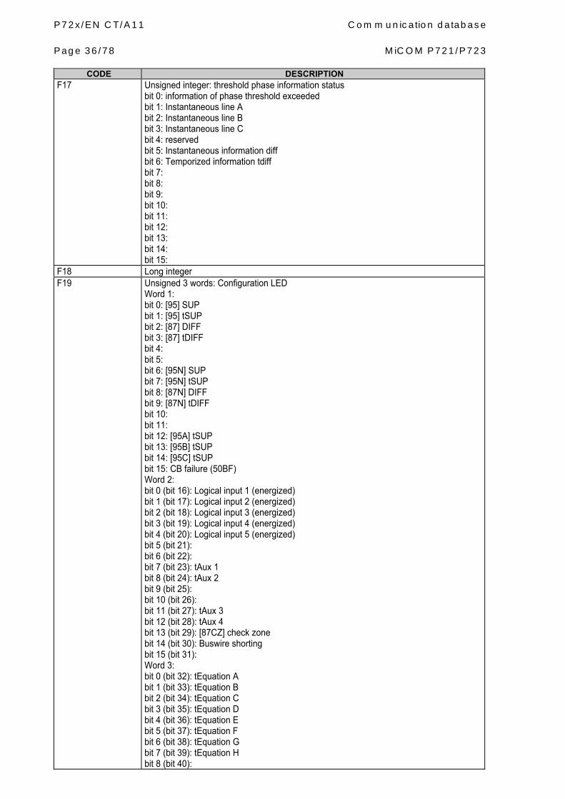
P72x/EN CT/A11 Communication database Page 36/78 MiCOM P721/P723
CODE DESCRIPTION F17 Unsigned integer: threshold phase information status
bit 0: information of phase threshold exceeded bit 1: Instantaneous line A bit 2: Instantaneous line B bit 3: Instantaneous line C bit 4: reserved bit 5: Instantaneous information diff bit 6: Temporized information tdiff bit 7: bit 8: bit 9: bit 10: bit 11: bit 12: bit 13: bit 14: bit 15:
F18 Long integer F19 Unsigned 3 words: Configuration LED
Word 1: bit 0: [95] SUP bit 1: [95] tSUP bit 2: [87] DIFF bit 3: [87] tDIFF bit 4: bit 5: bit 6: [95N] SUP bit 7: [95N] tSUP bit 8: [87N] DIFF bit 9: [87N] tDIFF bit 10: bit 11: bit 12: [95A] tSUP bit 13: [95B] tSUP bit 14: [95C] tSUP bit 15: CB failure (50BF) Word 2: bit 0 (bit 16): Logical input 1 (energized) bit 1 (bit 17): Logical input 2 (energized) bit 2 (bit 18): Logical input 3 (energized) bit 3 (bit 19): Logical input 4 (energized) bit 4 (bit 20): Logical input 5 (energized) bit 5 (bit 21): bit 6 (bit 22): bit 7 (bit 23): tAux 1 bit 8 (bit 24): tAux 2 bit 9 (bit 25): bit 10 (bit 26): bit 11 (bit 27): tAux 3 bit 12 (bit 28): tAux 4 bit 13 (bit 29): [87CZ] check zone bit 14 (bit 30): Buswire shorting bit 15 (bit 31): Word 3: bit 0 (bit 32): tEquation A bit 1 (bit 33): tEquation B bit 2 (bit 34): tEquation C bit 3 (bit 35): tEquation D bit 4 (bit 36): tEquation E bit 5 (bit 37): tEquation F bit 6 (bit 38): tEquation G bit 7 (bit 39): tEquation H bit 8 (bit 40):

Communication database P72x/EN CT/A11 MiCOM P721/P723 Page 37/78
CODE DESCRIPTION bit 9 (bit 41): bit 10 (bit 42): bit 11 (bit 43): bit 12 (bit 44): bit 13 (bit 45): bit 14 (bit 46): bit 15 (bit 47): Word 4: Not used
F20 Unsigned long: logical input settings and signalization Word 1: bit 0: bit 1: bit 2: Unlatch output relays bit 3: bit 4: bit 5: bit 6: Auxiliary input 1 bit 7: Auxiliary input 2 bit 8: Blocking logic 1 bit 9: Blocking logic 2 bit 10: Start disturbance bit 11: bit 12: Setting group 2 selection bit 13: bit 14: bit 15: Word 2: bit 0 (bit 16): bit 1 (bit 17): Reset of all alarms bit 2 (bit 18): Maintenance mode bit 3 (bit 19): Auxiliary input 3 bit 4 (bit 20): Auxiliary input 4 bit 5 (bit 21): bit 6 (bit 22): Local mode bit 7 (bit 23): Synchronization bit 8 (bit 24): [87CZ] check zone bit 9 (bit 25): bit 10 (bit 26): bit 11 (bit 27): bit 12 (bit 28): bit 13 (bit 29): bit 14 (bit 30): bit 15 (bit 31):
F21 Unsigned integer: software version 100: Version 10.A 101: Version 10.B 110: Version 11.A …
F22 Unsigned integer: Trip status bit 0: Trip output relay RL1 latched bit 1: Memorization of trip information bit 2 to bit 15: free
F23 Unsigned integer 8 bits: Device status bit 0: Device status bit 1: Minor material alarm bit 2: Presence of non-acknowledged event record bit 3: Synchronisation state bit 4: Presence of non-acknowledged disturbance record bit 5: Presence of non-acknowledged fault record bit 6: bit 7:

P72x/EN CT/A11 Communication database Page 38/78 MiCOM P721/P723
CODE DESCRIPTION F24 Unsigned integer: Status of the relay functions
0: Disabled / No 1: Enabled / Yes
F25 Reserved F26 Phases and Earth identifier
Phase1 Phase2 Phase3 0 : “L1” “L2” “L3” 1 : “ A” “ B” “ C” 2: “ R” “ S” “ T” Earth 0 : “ N” 1 : “ o” 2: “ E”
F27 Reserved F28 Unsigned integer: Rear port communication data bits
0: 7 data bits 1: 8 data bits
F29 Unsigned integer: Rear port communication stop bits 0: 1 stop bit 1: 2 stop bits
F30 Unsigned integer: Rear port communication available 0: Communication non-available 1: Communication available
F31 Reserved F32 Unsigned integer:
0: Disturbance record start condition on INSTANTANEOUS 1: Disturbance record start condition on TRIPPING
F33 Reserved F34 Reserved F35 Reserved F36 Unsigned 3 words: Memorised flags of non acknowledged alarms
Word 1 bit 0: [95N] SUP bit 1: [95N] tSUP bit 2: [87N] DIFF bit 3: [87N] tDIFF bit 4: bit 5: bit 6: [87CZ] check zone bit 7: Buswire shorting bit 8: bit 9: CB failure (50BF) bit 10: bit 11: bit 12: bit 13: tAux 1 bit 14: tAux 2 bit 15: Word 2 bit 0 (bit 16): bit 1 (bit 17): bit 2 (bit 18): bit 3 (bit 19): bit 4 (bit 20): bit 5 (bit 21): tAux 3 bit 6 (bit 22): tAux 4 bit 7 (bit 23): bit 8 (bit 24): bit 9 (bit 25): bit 10 (bit 26): bit 11 (bit 27): bit 12 (bit 28):

Communication database P72x/EN CT/A11 MiCOM P721/P723 Page 39/78
CODE DESCRIPTION bit 13 (bit 29): bit 14 (bit 30): bit 15 (bit 31): Word 3 bit 0 (bit 32): tEquation A bit 1 (bit 33): tEquation B bit 2 (bit 34): tEquation C bit 3 (bit 35): tEquation D bit 4 (bit 36): tEquation E bit 5 (bit 37): tEquation F bit 6 (bit 38): tEquation G bit 7 (bit 39): tEquation H bit 8 (bit 40): bit 9 (bit 42): bit 10 (bit 43): bit 11 (bit 44): bit 12 (bit 45): bit 13 (bit 46): bit 14 (bit 47):
F37 Reserved F38 Unsigned 2 words: Information of general status
Word 1: bit 0: Pole earth opening bit 1: CB failure (50BF) bit 2: Pole phase A opening bit 3: Pole phase B opening bit 4: Pole phase C opening bit 5: bit 6: tAux 1 bit 7: tAux 2 bit 8: bit 9: CB failure delay started (start tBF) bit 10: bit 11: bit 12: tAux 3 bit 13: tAux 4 bit 14: Buswires shorting bit 15: Word 2: bit 0 (bit 16): bit 1 (bit 17): bit 2 (bit 18): bit 3 (bit 19): bit 4 (bit 20): bit 5 (bit 21): bit 6 (bit 22): bit 7 (bit 23): bit 8 (bit 24): bit 9 (bit 25): bit 10 (bit 26): bit 11 (bit 27): bit 12 (bit 28): bit 13 (bit 29): bit 14 (bit 30): bit 15 (bit 31):
F39 Reserved F40 Reserved F41 Unsigned integer: Front/rear communication
0: Front and rear MODBUS communication 1: Front MODBUS and rear Courier communication 2: Front MODBUS and rear IEC 60870-5-103 communication 3: Front MODBUS and rear DNP3 communication

P72x/EN CT/A11 Communication database Page 40/78 MiCOM P721/P723
CODE DESCRIPTION F42 Reserved F43 Reserved F44 Reserved F45 Unsigned integer: Material alarm status
bit 0: Watch-Dog operating * bit 1: Communication failure bit 2: Program data failure * bit 3: Analogue input failure * bit 4: Datation failure bit 5: Calibration data failure * bit 6: Record data failure bit 7: bit 8: Maintenance Mode bit 9: Default settings alarm * bit 10: Inconsistent setting * bit 11: bit 12: bit 13: bit 14: bit 15: * Major alarm
F46 Reserved F47 Unsigned integer: Setting group change configuration
0: setting group change either by communication, or of the relay front (MENU) 1: setting group change on logical input state (LEVEL) of digital input.
F48 Unsigned integer: Communication date format 0: Private Format Date 1: IEC Format Date
F50 Unsigned integer: AC/DC voltage Type applied to the logical inputs 0: Direct current (DC) voltage 1: Alternative current (AC) voltage
F51 Unsigned integer: Setting group 1: Setting group 1 2: Setting group 2
F52 Reserved F53 Reserved F54 Reserved F55 Reserved F56 Unsigned integer : IEC870-5-103 messages option for non-standard protections
0 : Public messages 1 : Private messages.
F57 Reserved F58 Reserved F59 Unsigned integer : Inhibition of alarms
bit 0: Alarm tAux1 inhibited bit 1: Alarm tAux2 inhibited bit 2: Alarm tAux3 inhibited bit 3: Alarm tAux4 inhibited bit 4: bit 5: bit 6: bit 7: bit 8: bit 9: bit 10: bit 11: bit 12: bit 13: bit 14: bit 15:
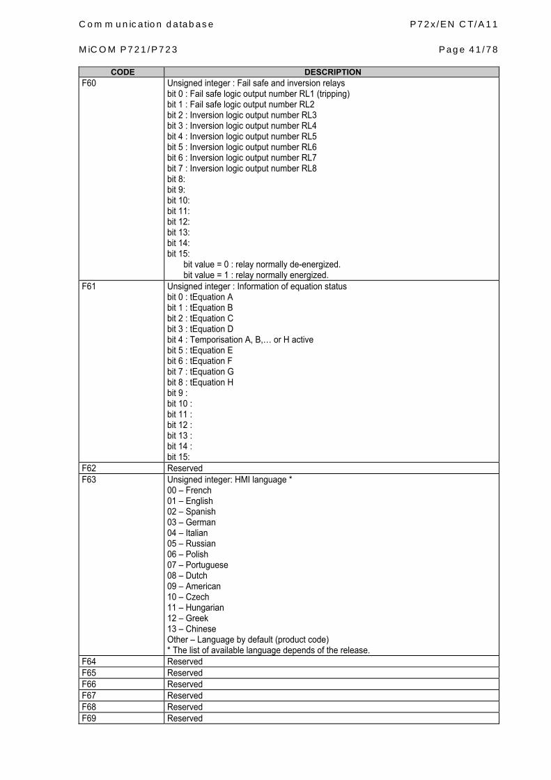
Communication database P72x/EN CT/A11 MiCOM P721/P723 Page 41/78
CODE DESCRIPTION F60 Unsigned integer : Fail safe and inversion relays
bit 0 : Fail safe logic output number RL1 (tripping) bit 1 : Fail safe logic output number RL2 bit 2 : Inversion logic output number RL3 bit 3 : Inversion logic output number RL4 bit 4 : Inversion logic output number RL5 bit 5 : Inversion logic output number RL6 bit 6 : Inversion logic output number RL7 bit 7 : Inversion logic output number RL8 bit 8: bit 9: bit 10: bit 11: bit 12: bit 13: bit 14: bit 15: bit value = 0 : relay normally de-energized. bit value = 1 : relay normally energized.
F61 Unsigned integer : Information of equation status bit 0 : tEquation A bit 1 : tEquation B bit 2 : tEquation C bit 3 : tEquation D bit 4 : Temporisation A, B,… or H active bit 5 : tEquation E bit 6 : tEquation F bit 7 : tEquation G bit 8 : tEquation H bit 9 : bit 10 : bit 11 : bit 12 : bit 13 : bit 14 : bit 15:
F62 Reserved F63 Unsigned integer: HMI language *
00 – French 01 – English 02 – Spanish 03 – German 04 – Italian 05 – Russian 06 – Polish 07 – Portuguese 08 – Dutch 09 – American 10 – Czech 11 – Hungarian 12 – Greek 13 – Chinese Other – Language by default (product code) * The list of available language depends of the release.
F64 Reserved F65 Reserved F66 Reserved F67 Reserved F68 Reserved F69 Reserved

P72x/EN CT/A11 Communication database Page 42/78 MiCOM P721/P723
CODE DESCRIPTION F70 Unsigned integer: 1st operator for Boolean equations
0 : NULL 1 : NOT
F71 Unsigned integer: Other than 1st operator for Boolean equations 0 : OR 1 : OR NOT 2 : AND 3 : AND NOT
F72 Unsigned integer: Operand for Boolean equations 0: NULL 1: [95] SUP 2: [95] tSUP 3: [95A] tSUP 4: [95B] tSUP 5: [95C] tSUP 6: [87] DIFF 7: [87] tDIFF 8: [95N] SUP 9: [95N] tSUP 10: [87N] DIFF 11: [87N] tDIFF 12: [87CZ] check zone 13: Buswire shorting 14: tAux 1 15: tAux 2 16: tAux 3 17: tAux 4 18: Logic input 1 (energized) 19: Logic input 2 (energized) 20: Logic input 3 (energized) 21: Logic input 4 (energized) 22: Logic input 5 (energized) 23: Active setting group 2 24: CB Failure
F73 Unsigned integer: LED status (bit = 0 if LED inactive) bit 0: Trip LED bit 1: Alarm LED bit 2: Warning LED bit 3: Healthy LED (always active) bit 4: LED 5 bit 5: LED 6 bit 6: LED 7 bit 7: LED 8 bit 8: bit 9: bit 10: bit 11: bit 12: bit 13: bit 14: bit 15:
F74 Unsigned integer: Filter of analogue input protection correspondence : 1: Sample mode only 3: Sample mode + Fast sample mode 4: Fourier mode (said differently: bit 0 is for Samples mode, bit 1 is for Fast samples mode, bit 2 is for Fourier mode)
F75 Unsigned integer: Diff. threshold unit mode 0: Current set (A) / Ampere 1: Voltage set (V) / Volt

Communication database P72x/EN CT/A11 MiCOM P721/P723 Page 43/78
CODE DESCRIPTION F76 Unsigned integer: Keyboard remote control word.
Only one bit simultaneously. The bit active simulate a pressure on the key. bit 0: CLEAR key bit 1: ALARM key bit 2: UP key bit 3: RIGHT key bit 4: ENTER key bit 5: DOWN key bit 6: LEFT key bit 7: bit 8: bit 9: bit 10: bit 11: bit 12: bit 13: bit 14: bit 15: Dialog re-init (factory test reserved)
F77 Unsigned integer: Phase/earth fault origin. 0: none 1: phase A 2: phase B 3: phase C 4: phases A-B 5: phases A-C 6: phases B-C 7: phases A-B-C 8: earth
F78 Unsigned integer: Fault recording starting origin (Trip origin). 0: none 1: Remote Control trip 2: 3: 4: [87] tDIFF 5: 6: 7: [87N] tDIFF 8: 9: 10: 11: tAux1 12: tAux2 13: 14: 15: tAux3 16: tAux4 17: 18: 19: tEquation A 20: tEquation B 21: tEquation C 22: tEquation D 23: tEquation E 24: tEquation F 25: tEquation G 26: tEquation H
F79 Unsigned integer: Differential protection type 0: Earth protection 1: Three-phase protection
F80 Unsigned integer: Spontaneous event enabling for IEC870-5-103 communication 0 : None 1 : IEC only 2 : All (IEC + Private)

P72x/EN CT/A11 Communication database Page 44/78 MiCOM P721/P723
CODE DESCRIPTION F81 Unsigned integer: Measurements transmission enabling for IEC870-5-103 communication
0 : None 1 : ASDU3.4 only 2: ASDU 9 only 3 : ASDU3.4 + ASDU 9
F82 Unsigned integer: Source of the disturbance recording start. 0 : None 1 : On trip protection 2: On instantaneous protection 3 : On communication order 4 : On logic input order 5 : No disturbance
4.1 Disturbance record additional information
4.1.1 MODBUS request definition used for disturbance record
To upload a disturbance record, the following requests must be done in the exact given order:
1. (optional): Send a request to know the number of disturbance records available in SRAM.
2. (compulsory): Send a request with the record number and the channel number.
3. (compulsory): Send one or several requests to upload the disturbance record data. It depends of the number of samples.
4. (compulsory): Send a request to upload the index frame.
4.1.2 Request to know the number of disturbance records in SRAM
Slave number Function code Word address Word number CRC
xx 03h 3Dh 00 00 24h xx xx
This request may be answered an error message with the error code:
EVT_NOK(OF): No record available
NOTA: If there is less than 5 records available, the answer will contains zero in the non-used words.
4.1.3 Service requests
This request must be send before uploading the disturbance record channel samples. It allows to know the record number and the channel number to upload. It allows also to know the number of samples in the channel.
Slave number Function code Word address Word number CRC
xx 03h Refer to mapping 00 0Bh xx xx
This request may be answered an error message with two different error codes:
CODE_DEF_RAM(02): SRAM failure
CODE_EVT_NOK(03): No disturbance record available in SRAM
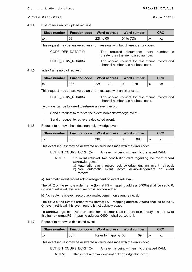
Communication database P72x/EN CT/A11 MiCOM P721/P723 Page 45/78 4.1.4 Disturbance record upload request
Slave number Function code Word address Word number CRC
xx 03h 22h to 00 01 to 7Dh xx xx
This request may be answered an error message with two different error codes:
CODE_DEP_DATA(04): The required disturbance data number is greater than the memorised number.
CODE_SERV_NOK(05): The service request for disturbance record and channel number has not been send.
4.1.5 Index frame upload request
Slave number Function code Word address Word number CRC
xx 03h 22h 00 00 07h xx xx
This request may be answered an error message with an error code:
CODE_SERV_NOK(05): The service request for disturbance record and channel number has not been send.
Two ways can be followed to retrieve an event record:
− Send a request to retrieve the oldest non-acknowledge event.
− Send a request to retrieve a dedicated event.
4.1.6 Request to retrieve the oldest non-acknowledge event
Slave number Function code Word address Word number CRC
xx 03h 36h 00 00 09h xx xx
This event request may be answered an error message with the error code:
EVT_EN_COURS_ECRIT (5): An event is being written into the saved RAM.
NOTE: On event retrieval, two possibilities exist regarding the event record acknowledgement: a) Automatic event record acknowledgement on event retrieval. b) Non automatic event record acknowledgement on event retrieval.
a) Automatic event record acknowledgement on event retrieval:
The bit12 of the remote order frame (format F9 – mapping address 0400h) shall be set to 0. On event retrieval, this event record is acknowledged.
b) Non automatic event record acknowledgement on event retrieval:
The bit12 of the remote order frame (format F9 – mapping address 0400h) shall be set to 1. On event retrieval, this event record is not acknowledged.
To acknowledge this event, an other remote order shall be sent to the relay. The bit 13 of this frame (format F9 – mapping address 0400h) shall be set to 1.
4.1.7 Request to retrieve a dedicated event
Slave number Function code Word address Word number CRC
xx 03h Refer to mapping 00 09h xx xx
This event request may be answered an error message with the error code:
EVT_EN_COURS_ECRIT (5): An event is being written into the saved RAM.
NOTA: This event retrieval does not acknowledge this event.
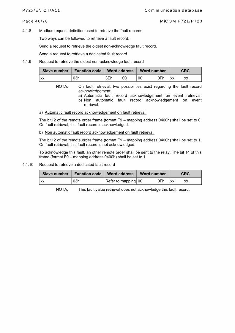
P72x/EN CT/A11 Communication database Page 46/78 MiCOM P721/P723 4.1.8 Modbus request definition used to retrieve the fault records
Two ways can be followed to retrieve a fault record:
Send a request to retrieve the oldest non-acknowledge fault record.
Send a request to retrieve a dedicated fault record.
4.1.9 Request to retrieve the oldest non-acknowledge fault record
Slave number Function code Word address Word number CRC
xx 03h 3Eh 00 00 0Fh xx xx
NOTA: On fault retrieval, two possibilities exist regarding the fault record acknowledgement: a) Automatic fault record acknowledgement on event retrieval. b) Non automatic fault record acknowledgement on event retrieval.
a) Automatic fault record acknowledgement on fault retrieval:
The bit12 of the remote order frame (format F9 – mapping address 0400h) shall be set to 0. On fault retrieval, this fault record is acknowledged.
b) Non automatic fault record acknowledgement on fault retrieval:
The bit12 of the remote order frame (format F9 – mapping address 0400h) shall be set to 1. On fault retrieval, this fault record is not acknowledged.
To acknowledge this fault, an other remote order shall be sent to the relay. The bit 14 of this frame (format F9 – mapping address 0400h) shall be set to 1.
4.1.10 Request to retrieve a dedicated fault record
Slave number Function code Word address Word number CRC
xx 03h Refer to mapping 00 0Fh xx xx
NOTA: This fault value retrieval does not acknowledge this fault record.

Communication database P72x/EN CT/A11 MiCOM P721/P723 Page 47/78
IEC 60870-5-103 DATABASE
MiCOM P721/P723 VERSION V11

P72x/EN CT/A11 Communication database Page 48/78 MiCOM P721/P723
BLANK PAGE

Communication database P72x/EN CT/A11 MiCOM P721/P723 Page 49/78
CONTENTS
1. IEC60870-5-103 INTERFACE 51
1.1 Physical connection and link layer 51 1.2 Link layer 51 1.3 Message validity check 52 1.4 IEC870-5-103 address 52 1.5 Initialisation 52 1.6 Time synchronisation 52 1.7 Spontaneous events 52 1.8 General interrogation 52 1.9 Cyclic measurements 53 1.10 Commands 53 1.11 Disturbance records 53 1.12 Blocking of monitor direction 53
2. APPENDIX 1 54
2.1 Spontaneous messages managed by MiCOM P72x 54 2.2 List of data contained in General Interrogation 57 2.3 Processed Commands 59 2.4 Relay re initialization 60 2.5 Cyclic Messages (Class 2 – measurements) 60 2.6 IEC870-5-103 messages for Disturbance record extraction 61

P72x/EN CT/A11 Communication database Page 50/78 MiCOM P721/P723
BLANK PAGE

Communication database P72x/EN CT/A11 MiCOM P721/P723 Page 51/78
5. IEC60870-5-103 INTERFACE The IEC60870-5-103 interface is a master/slave interface with the relay as the slave device. This protocol is based on the VDEW communication protocol. The relay conforms to compatibility level 2, compatibility level 3 is not supported.
The following IEC60870-5-103 facilities are supported by this interface:
• Initialisation (Reset)
• Time Synchronisation
• Event Record Extraction
• Disturbance Record Extraction
• General Interrogation
• Cyclic Measurements
• General Commands
5.1 Physical connection and link layer
Connection is available for IEC60870-5-103 through the rear RS485 port. It is possible to select both the relay address and baud rate using the front panel interface. Following a change, a reset command is required to re-establish communications.
The parameters of the communication are the following:
• Even Parity,
• 8 Data bits,
• 1 stop bit,
• Communication speed can be set in the front panel of the relay:
Baud rate (dec)
300
600
1200
2400
4800
9600
19200
38400
• Isolated two-point RS485 connection (2kV 50Hz),
• Asynchronous transmission.
To connect the relay after a parameter, speed, parity or address modification, a reset command is required.
5.2 Link layer
IEC870-5-103 frame conforms with IEC 870-5-FT1.2 standards. In addition, Special commands are added in accordance with IEC870-5-103 standard.

P72x/EN CT/A11 Communication database Page 52/78 MiCOM P721/P723 5.3 Message validity check
The validation of a frame is performed with a 16-bit Cyclical Redundancy Check (CRC). Generator polynomial: 1+x²+x15+x16 = 1010 0000 0000 0001 (binary) = A001 (hexadecimal)
5.4 IEC870-5-103 address
A slave address is defined in the range 1-254.
The address “255” is a standard address, frames with 255 are received by all slave devices.
5.5 Initialisation
Whenever the relay has been powered up, or if the communication parameters have been changed a reset command is required to initialise the communications. The relay will respond to either of the two reset commands (Reset CU or Reset FCB), the difference being that the Reset CU will clear any unsent messages in the relay’s transmit buffer.
The relay will respond to the reset command with an identification message ASDU 5, the Cause Of Transmission COT of this response will be either Reset CU or Reset FCB depending on the nature of the reset command. The following information will be contained in the data section of this ASDU:
Manufacturer Name: Schneider Electric
The Software Identification Section will contain the first four characters of the relay model number to identify the type of relay, e.g. P723.
In addition to the above identification message, if the relay has been powered up it will also produce a power up event.
5.6 Time synchronisation
The relay time and date can be set using the time synchronisation feature of the IEC60870-5-103 protocol. The relay will correct for the transmission delay as specified in IEC60870-5-103. If the time synchronisation message is sent as a send/confirm message then the relay will respond with a confirm. Whether the time synchronisation message is sent as a send confirm or a broadcast (send/no reply) message, a time synchronisation message will be returned as Class 1 data.
5.7 Spontaneous events
The events created by the relay will be passed using the standard function type/information numbers to the IEC60870-5-103 master station. Private codes are not used, thus any events that cannot be passed using the standardised messages will not be sent.
Events are categorised using the following information:
• Common Address
• Function Type
• Information number
• Cause of Transmission (to caracterise event origin).
APPENDIX 1 contains a complete listing of all events produced by the relay.
5.8 General interrogation
The GI request can be used to read the status of the relay, the function numbers, information numbers and common address offsets that will be returned during the GI cycle are indicated in APPENDIX 1.

Communication database P72x/EN CT/A11 MiCOM P721/P723 Page 53/78 5.9 Cyclic measurements
The relay will produce measured values using ASDU 9 and ASDU 3.4 on a cyclical basis, this can be read from the relay using a Class 2 poll.
It should be noted that the measurands transmitted by the relay are sent as a proportion of 2.4 times the rated value of the analogue value. The selection of either 1.2 or 2.4 for a particular value is indicated in APPENDIX 1.
5.10 Commands
A list of the supported commands is contained in APPENDIX 1. The relay will respond to other commands with an ASDU 1, with a cause of transmission (COT) of negative acknowledgement of a command. If the relay takes in account the command, it will answer with an ASDU 1, with a cause of transmission (COT) of positive acknowledgement.
A blocking command (Control directioncan be introduced using a communication parameter.
5.11 Disturbance records
The disturbance records stored by the relay cannot be extracted using the mechanism defined in the IEC60870-5-103 standard. A list of the analog channels and tags (logic signals) for record extraction is indicated in APPENDIX 1.
5.12 Blocking of monitor direction
The relay does not support a facility to block messages in the Monitor direction.IEC 60870-5-103 DATABASES

P72x/EN CT/A11 Communication database Page 54/78 MiCOM P721/P723
6. APPENDIX 1 6.1 Spontaneous messages managed by MiCOM P72x
These messages include a sub-assembly of events which are generated on the relay, because some generated events are not registered in VDEW. They are the most priority messages.
An event is always generated on the rising edge of the information.
Some events can be generated on the rising or lowering edge.
In the list below, events only generated on rising edge will be tagged with a ‘*’.
Two types of ASDU can be generated for events: ASDU 1 (time-tagged message) or ASDU 2 (time-tagged message with relative time).
The following list of processed events is the list with the private messages option active, for all Overcurrent protection functions, with the associated FUNCTION Type, INFORMATION NUMBER, ASDU TYPE, CAUSE OF TRANSMISSION and COMMON ADDRESS OF ASDU (The corresponding numbers with private messages option inactive are given just below).
FUN <208>: Function type in Public range for High-impedance Differential Protections (compatible).
FUN <210>: Function type in Private range (Reserved for High-impedance Differential Protections).
Status indications in monitor direction Availability
LEDs reset: FUN<208>;INF <19>; TYP <1>; COT<1>;<ADDR>,*
Local parameter Setting active: FUN<208>;INF <22>; TYP <1>; COT<1>,<ADDR>↑↓
Monitor direction blocked: FUN<208>;INF <20>; TYP <1>; COT<1>,<ADDR>↑↓
Command direction blocked: FUN<210>;INF <151>; TYP <1>; COT<1>,<ADDR>↑↓
Setting Group number 1 active: FUN<208>;INF <23>; TYP <1>; COT<1>,<ADDR>↑↓
Setting Group number 2 active: FUN<208>;INF <24>; TYP <1>; COT<1>,<ADDR>↑↓
Auxiliary input 1: FUN<208>;INF <27>; TYP <1>; COT<1>,<ADDR>↑↓
Auxiliary input 2: FUN<208>;INF <28>; TYP <1>; COT<1>,<ADDR>↑↓
Auxiliary input 3: FUN<208>;INF <29>; TYP <1>; COT<1>,<ADDR>↑↓
Auxiliary input 4: FUN<208>;INF <30>; TYP <1>; COT<1>,<ADDR>↑↓
Group Warning (Minor hardware alarm):
FUN<208>;INF <46>; TYP <1>; COT<1>,<ADDR>↑↓
Group Alarm (Major hardware alarm):
FUN<208>;INF <47>; TYP <1>; COT<1>,<ADDR>↑↓
Communication database P72x/EN CT/A11 MiCOM P721/P723 Page 55/78
Status indications in monitor direction Availability
Logical input 1: FUN<210>;INF <160>; TYP <1>; COT<1>,<ADDR>↑↓
Logical input 2: FUN<210>;INF <161>; TYP <1>; COT<1>,<ADDR>↑↓
Logical input 3: FUN<210>;INF <162>; TYP <1>; COT<1>,<ADDR>↑↓
Logical input 4: FUN<210>;INF <163>; TYP <1>; COT<1>,<ADDR>↑↓
Logical input 5: FUN<210>;INF <164>; TYP <1>; COT<1>,<ADDR>↑↓
Logical output 1: FUN<210>;INF <176>; TYP <1>; COT<1>,<ADDR>↑↓
Logical output 2: FUN<210>;INF <177>; TYP <1>; COT<1>,<ADDR>↑↓
Logical output 3: FUN<210>;INF <178>; TYP <1>; COT<1>,<ADDR>↑↓
Logical output 4: FUN<210>;INF <179>; TYP <1>; COT<1>,<ADDR>↑↓
Logical output 5 (Watch-dog): FUN<210>;INF <180>; TYP <1>; COT<1>,<ADDR>↑↓
Logical output 6: FUN<210>;INF <181>; TYP <1>; COT<1>,<ADDR>↑↓
Logical output 7: FUN<210>;INF <182>; TYP <1>; COT<1>,<ADDR>↑↓
Logical output 8: FUN<210>;INF <183>; TYP <1>; COT<1>,<ADDR>↑↓
Logical output 9: FUN<210>;INF <184>; TYP <1>; COT<1>,<ADDR>↑↓
Logical blocking 1: FUN<210>;INF <30>; TYP <1>; COT<1>,<ADDR>↑↓
Logical blocking 2: FUN<210>;INF <31>; TYP <1>; COT<1>,<ADDR>↑↓
Local mode active: FUN<210>;INF <40>; TYP <1>; COT<1>,<ADDR>↑↓
Time Synchronisation: FUN<210>;INF <226>; TYP <1>; COT<1>; <ADDR>,*
NOTE: The double arrow ↑↓ means that the event generated on event occurrence and another event is generated on event disappearing.

P72x/EN CT/A11 Communication database Page 56/78 MiCOM P721/P723
Supervision Indications in monitor direction
Availability
Start / pick-up [95] Diff>: FUN<210>;INF <9>; TYP <2>; COT<1>,<ADDR>↑↓
Start / pick-up [87] Diff>>: FUN<210>;INF <10>; TYP <2>; COT<1>,<ADDR>↑↓
Start / pick-up [95N] Diff>: FUN<210>;INF <12>; TYP <2>; COT<1>,<ADDR>↑↓
Start / pick-up [87N] Diff>>: FUN<210>;INF <13>; TYP <2>; COT<1>,<ADDR>↑↓
Start / pick-up Check Zone: FUN<210>;INF <24>; TYP <2>; COT<1>,<ADDR>↑↓
Start / pick-up Bus Wire Shorting:
FUN<210>;INF <26>; TYP <2>; COT<1>,<ADDR>↑↓
General Trip: FUN<208>;INF <68>; TYP <2>; COT<1>,<ADDR>,*
General Start / pick-up: FUN<208>;INF <84>; TYP <2>; COT<1>,<ADDR>↑↓
Breaker failure: FUN<208>;INF <85>; TYP <2>; COT<1>,<ADDR>,*
Trip [95] Diff>: FUN<210>;INF <17>; TYP <2>; COT<1>,<ADDR>,*
Trip [95A] Diff>: FUN<210>;INF <42>; TYP <2>; COT<1>,<ADDR>,*
Trip [95B] Diff>: FUN<210>;INF <43>; TYP <2>; COT<1>,<ADDR>,*
Trip [95C] Diff>: FUN<210>;INF <44>; TYP <2>; COT<1>,<ADDR>,*
Trip [87] Diff>>: FUN<210>;INF <18>; TYP <2>; COT<1>,<ADDR>,*
Trip [95N] Diff>: FUN<210>;INF <20>; TYP <2>; COT<1>,<ADDR>,*
Trip [87N] Diff>>: FUN<210>;INF <21>; TYP <2>; COT<1>,<ADDR>,*
Trip Equation A: FUN<210>;INF <144>; TYP <2>;COT<1>,<ADDR>,↑↓
Trip Equation B: FUN<210>;INF <145>; TYP <2>;COT<1>,<ADDR>,↑↓
Trip Equation C: FUN<210>;INF <146>; TYP <2>;COT<1>,<ADDR>,↑↓
Trip Equation D: FUN<210>;INF <147>; TYP <2>;COT<1>,<ADDR>,↑↓
Trip Equation E: FUN<210>;INF <196>; TYP <2>;COT<1>,<ADDR>,↑↓
Trip Equation F: FUN<210>;INF <197>; TYP <2>;COT<1>,<ADDR>,↑↓

Communication database P72x/EN CT/A11 MiCOM P721/P723 Page 57/78
Supervision Indications in monitor direction
Availability
Trip Equation G: FUN<210>;INF <198>; TYP <2>;COT<1>,<ADDR>,↑↓
Trip Equation H: FUN<210>;INF <199>; TYP <2>;COT<1>,<ADDR>,↑↓
NOTE: The double arrow ↑↓ means that the event generated on event occurrence and another event is generated on event disappearing.
Auto-recloser Indications (monitor direction)
Availability
Trip TC: FUN<210>;INF <1>; TYP <1>; COT<1>,<ADDR>↑↓
NOTE: The double arrow ↑↓ means that the event generated on event occurrence and another event is generated on event disappearing.
6.2 List of data contained in General Interrogation
It is given in the answer to the General Interrogation (GI).
Relay state information are Class 1 data, they are systematically sent to the master station, during a General Interrogation.
The list of processed data, following a General Interrogation, is given below: it is a sub-assembly of the spontaneous message list, so like spontaneous messages, these data are generated on rising and lowering edge.
Status indications (monitor direction):
Status Indications (monitor direction):
Status Indications (monitor direction)
Availability
Local parameter Setting active: FUN<208>;INF <22>; TYP <1>; COT<9>,<ADDR>
Monitor direction blocked: FUN<208>;INF <20>; TYP <1>; COT<9>,<ADDR>
Setting Group number 1 active: FUN<208>;INF <23>; TYP <1>; COT<9>,<ADDR>
Setting Group number 2 active: FUN<208>;INF <24>; TYP <1>; COT<9>,<ADDR>
Auxiliary input 1: FUN<208>;INF <27>; TYP <1>; COT<9>,<ADDR>
Auxiliary input 2: FUN<208>;INF <28>; TYP <1>; COT<9>,<ADDR>
Auxiliary input 3: FUN<208>;INF <29>; TYP <1>; COT<9>,<ADDR>
Auxiliary input 4: FUN<208>;INF <30>; TYP <1>; COT<9>,<ADDR>
P72x/EN CT/A11 Communication database Page 58/78 MiCOM P721/P723
Status Indications (monitor direction)
Availability
Group Warning (Minor hardware alarm):
FUN<208>;INF <46>; TYP <1>; COT<9>,<ADDR>
Group Alarm (Major hardware alarm):
FUN<208>;INF <47>; TYP <1>; COT<9>,<ADDR>
General Start / pick-up: FUN<208>;INF <84>; TYP <2>; COT<9>,<ADDR>
Command direction blocked: FUN<210>;INF <151>; TYP <1>; COT<9>,<ADDR>
Maintenance mode trig: FUN<210>;INF <7>; TYP <1>; COT<9>,<ADDR>
Fault Indications in monitor direction
Availability
Start / pick-up [95] Diff>: FUN<210>;INF <9>; TYP <2>; COT<9>,<ADDR>
Start / pick-up [87] Diff>>: FUN<210>;INF <10>; TYP <2>; COT<9>,<ADDR>
Start / pick-up [95N] Diff >: FUN<210>;INF <12>; TYP <2>; COT<9>,<ADDR>
Start / pick-up [87N] Diff>>: FUN<210>;INF <13>; TYP <2>; COT<9>,<ADDR>
Start / pick-up Check Zone: FUN<210>;INF <24>; TYP <2>; COT<9>,<ADDR>
Start / pick-up Bus Wire Shorting: FUN<210>;INF <26>; TYP <2>; COT<9>,<ADDR>
Status Indications in monitor direction Availability
Logical input 1: FUN<210>;INF <160>; TYP <1>; COT<9>,<ADDR>
Logical input 2: FUN<210>;INF <161>; TYP <1>; COT<9>,<ADDR>
Logical input 3: FUN<210>;INF <162>; TYP <1>; COT<9>,<ADDR>
Logical input 4: FUN<210>;INF <163>; TYP <1>; COT<9>,<ADDR>
Logical input 5: FUN<210>;INF <164>; TYP <1>; COT<9>,<ADDR>
Logical output 1: FUN<210>;INF <176>; TYP <1>; COT<9>,<ADDR>
Logical output 2: FUN<210>;INF <177>; TYP <1>; COT<9>,<ADDR>
Logical output 3: FUN<210>;INF <178>; TYP <1>; COT<9>,<ADDR>

Communication database P72x/EN CT/A11 MiCOM P721/P723 Page 59/78
Status Indications in monitor direction Availability
Logical output 4: FUN<210>;INF <179>; TYP <1>; COT<9>,<ADDR>
Logical output 5 (Watch-dog): FUN<210>;INF <180>; TYP <1>; COT<9>,<ADDR>
Logical output 6: FUN<210>;INF <181>; TYP <1>; COT<9>,<ADDR>
Logical output 7: FUN<210>;INF <182>; TYP <1>; COT<9>,<ADDR>
Logical output 8: FUN<210>;INF <183>; TYP <1>; COT<9>,<ADDR>
Logical output 9: FUN<210>;INF <184>; TYP <1>; COT<9>,<ADDR>
6.3 Processed Commands
System Commands Availability Synchronization Command (ASDU 6)
FUN<255>,INF <0>; TYP <6>;COT<8>
This command can be sent to a specific relay, or global. The time sent by master is the time of the first bit of the frame. The relay synchronizes with this time, corrected by the frame transmission delay. After updating its time, the relay send back an acknowledge to the master, by giving its new current time. This acknowledge message will be an event of ASDU 6 type.
− General Interrogation Initialization command (ASDU 7):
This command starts the relay interrogation:
− The relay then sends a list of data containing the relay state (see list described above).
− The GI command contains a scan number which will be included in the answers of the GI cycle generated by the GI command.
If a data has just changed before extracted by the GI, the new state is sent to the master station.
When an event is generated during the GI cycle, the event is sent in priority, and the GI cycle is temporarily interrupted. The end of the GI consists in sending an ASDU 8 to the master station.
If, during a General Interrogation cycle, another GI Initialization command is received, the precedent answer is stopped, and the new GI cycle started.
General Commands (ASDU 20) (Control Direction)
Availability
LEDs Reset: This command acknowledge all alarms on Front Panel on MiCOM P72x products:
FUN<208>;INF<19>, TYP<20>, COT <20>,<ADDR>
Setting group number 1: FUN<208>;INF<23>, TYP<20>, COT <20>,<ADDR>
Setting group number 2: FUN<208>;INF<24>, TYP<20>, COT <20>,<ADDR>

P72x/EN CT/A11 Communication database Page 60/78 MiCOM P721/P723
General Commands (ASDU 20) (Control Direction)
Availability
Trip TC: FUN<210>;INF <1>; TYP <20>; COT<20>,<ADDR>
Disturbance trig: FUN<210>;INF <3>; TYP <20>; COT<20>,<ADDR>
Maintenance mode trig: FUN<210>;INF <7>; TYP <20>; COT<20>,<ADDR>
After executing one of these commands, the relay sends an acknowledge message, which contains the result of command execution.
If a state change is the consequence of the command, it must be sent in a ASDU 1 with COT 12 (remote operation).
If the relay receive another command message from the master station before sending the acknowledge message, it will be discarded.
Commands which are not processed by the relay are rejected with a negative acknowledge message.
6.4 Relay re initialization
In case of relay re initialization, the relay send to the master station:
Availability A message indicating relay start/restart:
(FUN<208>;INF <5>; TYP <5> COT <5>)
or a message indicating Reset CU:
(FUN<208>;INF <5>; TYP <3> COT <4>)
or a message indicating Reset FCB :
(FUN<208>;INF <5>; TYP <2> COT <3>)
Each identification message of the relay (ASDU 5) contains the manufacturer name in 8 ASCII characters and 2 free bytes containing: « 721 » or « 723 »,in decimal format, then 2 free bytes containing the software version number in decimal (for ex. : 112 corresponds to “11.C”).
6.5 Cyclic Messages (Class 2 – measurements)
Only measurands can be stored in these messages.
The measurands values are stored in lower levels of communication, before polling by master station.
Measurands I1,I2,I3,V1,V2,V3, P, Q FUN<208>;INF <148>; TYP <9>; COT<2>,<ADDR>
Several of the fields in the ASDU 9 are not used (Voltage and Power values), so they are set to 0: Only RMS Ia, Ib, Ic values and frequency are stored (with a rate such as: 2,4 * nominal value = 4096).
Measurands In, Ven FUN<208>;INF <147>; TYP <3>; COT<2>,<ADDR>
The second ASDU is ASDU3.4 (STRUCT<2>), which contains in first position In earth current value in rated format (with a rate such as: 2,4 * nominal value = 4096). Ven value does not exist, so the second position value in ASDU3.4 is set to « unused ».

Communication database P72x/EN CT/A11 MiCOM P721/P723 Page 61/78
6.6 IEC870-5-103 messages for Disturbance record extraction
The disturbance extraction procedure with IEC870-5-103 in MICOM Px2x relays is in conformance with IEC870-5-103 standard definition. The maximum disturbance record number stored in a P721 and P723 is 5.
The disturbance record mapping is the following:
− 4 analog channels:
• Channel 1: Ia current (Phase L1).
• Channel 2: Ib current (Phase L2).
• Channel 3: Ic current (Phase L3).
• Channel 4: IN current (Earth).
− 12 Identifiers of tags transmitted in ASDU 29 (logical informations):
• Tag number 1: General start: FUN <208> INF <84>
• Tag number 2: CB Failure: FUN <208> INF <85>
• Tag number 3: General Trip: FUN <208> INF <68>
• Tag number 4: [95] Diff>: FUN <210> INF <17>
• Tag number 5: [87] Diff>>: FUN <210> INF <18>
• Tag number 6 [95N] Diff>: FUN <210> INF <20>
• Tag number 7 [87N] Diff>>: FUN <210> INF <21>
• Tag number 8 Log input 1: FUN <210> INF <160>
• Tag number 9 Log input 2: FUN <210> INF <161>
• Tag number 10 Log input 3: FUN <210> INF <162>
• Tag number 11 Log input 4: FUN <210> INF <163>
• Tag number 12 Log input 5: FUN <210> INF <164>

P72x/EN CT/A11 Communication database Page 62/78 MiCOM P721/P723
BLANK PAGE

Communication database P72x/EN CT/A11 MiCOM P721/P723
DNP 3.0 DATABASE MiCOM P721/P723
VERSION V11

P72x/EN CT/A11 Communication database Page 64/78 MiCOM P721/P723
BLANK PAGE

Communication database P72x/EN CT/A11 MiCOM P721/P723 Page 65/78
CONTENTS
1. INTRODUCTION 67
1.1 Purpose of this document 67 1.2 DNP V3.00 device Profile 67 1.3 Implementation Table 70 1.4 Point List 72 1.4.1 Binary Input Points 72 1.4.2 Binary Output Status Points and Control Relay Output Blocks 74 1.4.3 Counters 75 1.4.4 Analog Inputs 76

P72x/EN CT/A11 Communication database Page 66/78 MiCOM P721/P723
BLANK PAGE
Communication database P72x/EN CT/A11 MiCOM P721/P723 Page 67/78
1. INTRODUCTION
1.1 Purpose of this document
The purpose of this document is to describe the specific implementation of the Distributed Network Protocol (DNP) 3.0 within P72x MiCOM relays.
P72x uses the Triangle MicroWorks, Inc. DNP 3.0 Slave Source Code Library Version 2.18.
This document, in conjunction with the DNP 3.0 Basic 4 Document Set, and the DNP Subset Definitions Document, provides complete information on how to communicate with P72x via the DNP 3.0 protocol.
This implementation of DNP 3.0 is fully compliant with DNP 3.0 Subset Definition Level 2, contains many Subset Level 3 features, and contains some functionality even beyond Subset Level 3.
1.2 DNP V3.00 device Profile
The following table provides a “Device Profile Document” in the standard format defined in the DNP 3.0 Subset Definitions Document. While it is referred to in the DNP 3.0 Subset Definitions as a “Document,” it is only a component of a total interoperability guide. This table, in combination with the following should provide a complete interoperability/configuration guide for P72x:
• the Implementation Table provided in Section 1.3 (beginning on page 70),
• the Point List Tables provided in Section 1.4 (beginning on page 72),
• and a description of configuration methods and user-interface in Sections

P72x/EN CT/A11 Communication database Page 68/78 MiCOM P721/P723
DNP V3.00
DEVICE PROFILE DOCUMENT
(ALSO SEE THE IMPLEMENTATION TABLE IN SECTION 1.3, BEGINNING ON PAGE 70). Vendor Name: Schneider Electric Device Name: SERIAL 20 Platform using the Triangle MicroWorks, Inc. DNP 3.0 Slave
Source Code Library, Version 2.18. Highest DNP Level Supported: For Requests: Level 2 For Responses: Level 2
Device Function: Master Slave
Notable objects, functions, and/or qualifiers supported in addition to the Highest DNP Levels Supported (the complete list is described in the attached table): For static (non-change-event) object requests, request qualifier codes 00 and 01 (start-stop), 07 and 08 (limited quantity), and 17 and 28 (index) are supported in addition to request qualifier code 06 (no range – or all points). Static object requests received with qualifiers 00, 01, 06, 07, or 08, will be responded with qualifiers 00 or 01. Static object requests received with qualifiers 17 or 28 will be responded with qualifiers 17 or 28. For change-event object requests, qualifiers 17 or 28 are always responded. 16-bit and 32-bit Analog Change Events with Time may be requested. The read function code for Object 50 (Time and Date), variation 1, is supported. Maximum Data Link Frame Size (octets): Transmitted: 292 Received 292
Maximum Application Fragment Size (octets): Transmitted: 2048 Received: 2048
Maximum Data Link Re-tries: None Fixed at 2 Configurable
Maximum Application Layer Re-tries: None Configurable
Requires Data Link Layer Confirmation: Never Always Sometimes Configurable Requires Application Layer Confirmation: Never Always When reporting Event Data When sending multi-fragment responses Sometimes Configurable Timeouts while waiting for: Data Link Confirm: None Fixed (100 ms) Variable Configurable. Complete Appl. Fragment: None Fixed at ____ Variable Configurable Application Confirm: None Fixed (1s) Variable Configurable Complete Appl. Response: None Fixed at ____ Variable Configurable Others: Binary input change scanning period: 5ms Analog input change scanning period: 1s

Communication database P72x/EN CT/A11 MiCOM P721/P723 Page 69/78
DNP V3.00
DEVICE PROFILE DOCUMENT
(ALSO SEE THE IMPLEMENTATION TABLE IN SECTION 1.3, BEGINNING ON PAGE 70). Sends/Executes Control Operations: WRITE Binary Outputs Never Always Sometimes Configurable SELECT/OPERATE Never Always Sometimes Configurable DIRECT OPERATE Never Always Sometimes Configurable DIRECT OPERATE – NO ACK Never Always Sometimes Configurable Count > 1 Never Always Sometimes Configurable Pulse On Never Always Sometimes Configurable Pulse Off Never Always Sometimes Configurable Latch On Never Always Sometimes Configurable Latch Off Never Always Sometimes Configurable Queue Never Always Sometimes Configurable Clear Queue Never Always Sometimes Configurable Reports Binary Input Change Events when no specific variation requested: Never Only time-tagged for P721 and
P723 Only non-time-tagged Configurable
Reports time-tagged Binary Input Change Events when no specific variation requested: Never Binary Input Change With Time for
P721 and P723 Binary Input Change With Relative Time Configurable (attach explanation)
Sends Unsolicited Responses: Never Configurable Only certain objects Sometimes (attach explanation) ENABLE/DISABLE UNSOLICITED
Function codes supported
Sends Static Data in Unsolicited Responses: Never When Device Restarts When Status Flags Change No other options are permitted.
Default Counter Object/Variation: No Counters Reported Configurable Default Object: 20 Default Variation: 5 Point-by-point list attached
Counters Roll Over at: No Counters Reported Configurable (attach explanation) 16 Bits 32 Bits Other Value: _____ Point-by-point list attached
Sends Multi-Fragment Responses: Yes No

P72x/EN CT/A11 Communication database Page 70/78 MiCOM P721/P723
1.3 Implementation Table
The following table identifies the variations, function codes, and qualifiers supported by the P72x in both request messages and in response messages.
For static (non-change-event) objects, requests sent with qualifiers 00, 01, 06, 07, or 08, will be responded with qualifiers 00 or 01. Static object requests sent with qualifiers 17 or 28 will be responded with qualifiers 17 or 28. For change-event objects, qualifiers 17 or 28 are always responded.
In the table below the text shaded as indicates Subset Level 3 functionality Subset Level 3
(beyond Subset Level 2), and text shaded as beyond Subset Level 3
Indicates functionality
beyond Subset Level 3.
OBJECT REQUEST (Library will parse)
RESPONSE (Library will respond with)
Object Number
Variation Number Description Function Codes
(dec) Qualifier
Codes (hex) Function
Codes (dec) Qualifier
Codes (hex) 1 0 Binary Input (Variation 0 is used
to request default variation) 1 (read)
00, 01 (start-stop) 06 (no range, or all) 07, 08 (limited qty) 17, 28 (index)
1 1 (default –
see note 1)
Binary Input 1 (read) 22
00, 01 (start-stop) 06 (no range, or all) 07, 08 (limited qty) 17, 28 (index)
129 (response) 00, 01 (start-stop) 17, 28 (index – see note 2)
1 2 Binary Input with Status 1 (read)
00, 01 (start-stop) 06 (no range, or all) 07, 08 (limited qty) 17, 28 (index
129 (response) 00, 01 (start-stop) 17, 28 (index – see note 2)
2 0 Binary Input Change (Variation 0 is used to request default variation)
1 (read) 06 (no range, or all) 07, 08 (limited qty)
2 1(default – see note1)
Binary Input Change without Time
1 (read) 06 (no range, or all) 07, 08 (limited qty)
129 (response)
17, 28 (index)
2
2 (default –
see note 1)
Binary Input Change with Time 1 (read) 06 (no range, or all) 07, 08 (limited qty)
129 (response)
17, 28 (index)
10 0 Binary Output Status (Variation 0 is used to request default variation)
1 (read) 00, 01 (start-stop) 06 (no range, or all) 07, 08 (limited qty) 17, 28 (index)
10 2 (default –
see note 1)
Binary Output Status 1 (read)
00, 01 (start-stop) 06 (no range, or all) 07, 08 (limited qty) 17, 28 (index)
129 (response) 00, 01 (start-stop) 17, 28 (index – see note 2)
12 1 Control Relay Output Block 3 (select) 4 (operate) 5 (direct op) 6 (dir. op, noack)
00, 01 (start-stop) 07, 08 (limited qty) 17, 28 (index)
129 (response) echo of request
20
0 Binary Counter (Variation 0 is used to request default variation)
1 (read) 7 (freeze) 8 (freeze noack) 9 (freeze clear) 10 (frz. cl. Noack)
00, 01 (start-stop) 06 (no range, or all) 07, 08 (limited qty) 17, 28 (index)
20
1 32-Bit Binary Counter 1 (read) 7 (freeze) 8 (freeze noack) 9 (freeze clear) 10 (frz. cl. Noack)
00, 01 (start-stop) 06 (no range, or all) 07, 08 (limited qty) 17, 28 (index)
129 (response) 00, 01 (start-stop) 17, 28 (index – see note 2)
20
2 16-Bit Binary Counter 1 (read) 7 (freeze) 8 (freeze noack) 9 (freeze clear) 10 (frz. cl. Noack)
00, 01 (start-stop) 06 (no range, or all) 07, 08 (limited qty) 17, 28 (index)
129 (response) 00, 01 (start-stop) 17, 28 (index – see note 2)
20
5 32-Bit Binary Counter without Flag
1 (read) 7 (freeze) 8 (freeze noack) 9 (freeze clear) 10 (frz. cl. Noack)
00, 01 (start-stop) 06 (no range, or all) 07, 08 (limited qty) 17, 28 (index)
129 (response) 00, 01 (start-stop) 17, 28 (index – see note 2)
20
6 16-Bit Binary Counter without Flag
1 (read) 7 (freeze) 8 (freeze noack) 9 (freeze clear) 10 (frz. cl. Noack)
00, 01 (start-stop) 06 (no range, or all) 07, 08 (limited qty) 17, 28 (index)
129 (response) 00, 01 (start-stop) 17, 28 (index – see note 2)

Communication database P72x/EN CT/A11 MiCOM P721/P723 Page 71/78
OBJECT REQUEST (Library will parse)
RESPONSE (Library will respond with)
Object Number
Variation Number Description Function Codes
(dec) Qualifier
Codes (hex) Function
Codes (dec) Qualifier
Codes (hex) 21
0 Frozen Counter (Variation 0 is used to request default variation)
1 (read) 00, 01 (start-stop) 06 (no range, or all) 07, 08 (limited qty) 17, 28 (index)
21
1 32-Bit Frozen Counter 1 (read)
00, 01 (start-stop) 06 (no range, or all) 07, 08 (limited qty) 17, 28 (index)
129 (response) 00, 01 (start-stop) 17, 28 (index – see note 2)
21
2 16-Bit Frozen Counter 1 (read)
00, 01 (start-stop) 06 (no range, or all) 07, 08 (limited qty) 17, 28 (index)
129 (response) 00, 01 (start-stop) 17, 28 (index – see note 2)
21
9 32-Bit Frozen Counter without Flag
1 (read)
00, 01 (start-stop) 06 (no range, or all) 07, 08 (limited qty) 17, 28 (index)
129 (response) 00, 01 (start-stop) 17, 28 (index – see note 2)
21
10 16-Bit Frozen Counter without Flag
1 (read)
00, 01 (start-stop) 06 (no range, or all) 07, 08 (limited qty) 17, 28 (index)
129 (response) 00, 01 (start-stop) 17, 28 (index – see note 2)
30 0 Analog Input (Variation 0 is used to request default variation)
1 (read)
00, 01 (start-stop) 06 (no range, or all) 07, 08 (limited qty) 17, 28 (index)
30 1 (default – see note 1
32-Bit Analog Input 1 (read)
00, 01 (start-stop) 06 (no range, or all) 07, 08 (limited qty) 17, 28 (index)
129 (response) 00, 01 (start-stop) 17, 28 (index – see note 2)
30 2
16-Bit Analog Input 1 (read)
00, 01 (start-stop) 06 (no range, or all) 07, 08 (limited qty) 17, 28 (index)
129 (response) 00, 01 (start-stop) 17, 28 (index – see note 2)
30 3 32-Bit Analog Input without Flag 1 (read)
00, 01 (start-stop) 06 (no range, or all) 07, 08 (limited qty) 17, 28 (index)
129 (response) 00, 01 (start-stop) 17, 28 (index – see note 2)
30 4 16-Bit Analog Input without Flag 1 (read)
00, 01 (start-stop) 06 (no range, or all) 07, 08 (limited qty) 17, 28 (index)
129 (response) 00, 01 (start-stop) 17, 28 (index – see note 2)
32
0 Analog Change Event (Variation 0 is used to request default variation)
1 (read) 06 (no range, or all) 07, 08 (limited qty)
32 1 (default –
see note 1)
32-Bit Analog Change Event without Time
1 (read)
06 (no range, or all) 07, 08 (limited qty)
129 (response)
17, 28 (index)
32 2
16-Bit Analog Change Event without Time
1 (read)
06 (no range, or all) 07, 08 (limited qty)
129 (response)
17, 28 (index)
32
3 32-Bit Analog Change Event with Time
1 (read)
06 (no range, or all) 07, 08 (limited qty)
129 (response) 17, 28 (index)
32
4 16-Bit Analog Change Event with Time
1 (read)
06 (no range, or all) 07, 08 (limited qty)
129 (response) 17, 28 (index)
50
0 Time and Date 1 (read)
00, 01 (start-stop) 06 (no range, or all) 07, 08 (limited qty) 17, 28 (index)
129 (response)
00, 01 (start-stop) 17, 28 (index – see note 2)
50
1 (default –
see note 1)
Time and Date 1 (read) 2 (write)
00, 01 (start-stop) 06 (no range, or all) 07 (limited qty=1) 08 (limited qty) 17, 28 (index)
129 (response)
00, 01 (start-stop) 17, 28 (index – see note 2)
52 2 Time Delay Fine 129 (response) 07 (limited qty) (qty = 1)
60 0 Class 0, 1, 2, and 3 Data 1 (read)
06 (no range, or all)
60 1 Class 0 Data 1 (read)
06 (no range, or all) 129 17,28
60 2 Class 1 Data 1 (read) 06 (no range, or all) 07, 08 (limited qty)
129 17,28
60 3 Class 2 Data 1 (read)
06 (no range, or all) 07, 08 (limited qty)
129 17,28
60 4 Class 3 Data 1 (read)
06 (no range, or all) 07, 08 (limited qty)
129 17,28
80 1 Internal Indications 2 (write) 00 (start-stop) (index must =7)
No Object (function code only) –See Note 3
13 (cold restart)
No Object (function code only) 14 (warm restart)
No Object (function code only) 23 (delay meas.)
Note 1: A Default variation refers to the variation responded when variation 0
is requested and/or in class 0, 1, 2, or 3 scans.

P72x/EN CT/A11 Communication database Page 72/78 MiCOM P721/P723
Note 2: For static (non-change-event) objects, qualifiers 17 or 28 are only responded when a request is sent with qualifiers 17 or 28, respectively. Otherwise, static object requests sent with qualifiers 00, 01, 06, 07, or 08, will be responded with qualifiers 00 or 01. (For change-event objects, qualifiers 17 or 28 are always responded.)
Note 3: For P72x, a cold restart is implemented as a warm restart – the executable is not restarted, but the DNP process is restarted.
1.4 Point List
The tables in the following sections identify all the individual data points provided by this implementation of DNP 3.0. uses the database protection.
1.4.1 Binary Input Points
Every Binary Input Status points are included in class 0 polls, because they are included in one of classes 1, 2 or 3.
Binary Input Points Static (Steady-State) Object Number: 1 Change Event Object Number: 2 Request Function Codes supported: 1 (read) Static Variation reported when variation 0 requested: 1 (Binary Input without status) Change Event Variation reported when variation 0 requested: 2 (Binary Input Change with Time) for P721 and P723
P72x Point Index
P721 Presence
P723 Presence Name/Description init val.
Change Event Class (1, 2, 3 or
none)
0 X X Output relay 1 (trip) 0 1
1 X X Output relay 2 0 2
2 X X Output relay 3 0 2
3 X X Output relay 4 0 2
4 X X Output relay 0 ( watch dog) 0 2
5 X Output relay 5 0 2
6 X Output relay 6 0 2
7 X Output relay 7 0 2
8 X Output relay 8 0 2
9 X X Opto isolator 1 0 2
10 X X Opto isolator 2 0 2
11 X Opto isolator 3 0 2
12 X Opto isolator 4 0 2
13 X Opto isolator 5 0 2
14 X [95] diff> start 0 1
15 X [95] tdiff> trip 0 1
16 X [87] diff>> start 0 1
17 X [87] tdiff>> trip 0 1
18 X X [95N] diff> start 0 1
19 X X [95N] tdiff> trip 0 1
20 X X [87N] diff>> start 0 1
21 X X [87N] tdiff>> trip 0 1
22 X X [87CZ] check zone 0 1
23 X X Buswire shorting 0 1
24 X X tAux1 0 1
25 X X tAux2 0 1
26 X X tAux3 0 1
27 X X tAux4 0 1
28 X X Blocking Logic 1 0 1

Communication database P72x/EN CT/A11 MiCOM P721/P723 Page 73/78 Binary Input Points Static (Steady-State) Object Number: 1 Change Event Object Number: 2 Request Function Codes supported: 1 (read) Static Variation reported when variation 0 requested: 1 (Binary Input without status) Change Event Variation reported when variation 0 requested: 2 (Binary Input Change with Time) for P721 and P723
P72x Point Index
P721 Presence
P723 Presence Name/Description init val.
Change Event Class (1, 2, 3 or
none)
29 X X Blocking Logic 2 0 1
30 X X De latching by a logic input 0 1
31 X X De latching of the Tripping output relay by remote order 0 1
32 X X Tripping order by remote order 0 1
33 X CB Failure (50BF) 0 1
34 X X tEquation A 0 1
35 X X tEquation B 0 1
36 X X tEquation C 0 1
37 X X tEquation D 0 1
38 X X tEquation E 0 1
39 X X tEquation F 0 1
40 X X tEquation G 0 1
41 X X tEquation H 0 1
42 X X Shifting to maintenance mode 0 1
43 X X Major material Alarms 0 1
44 X X Minor material Alarms 0 1
45 X X Latching of Relay 0 2
46 X [95] tdiff> trip alarm (latched) 0 3
47 X [87] tdiff>> trip alarm (latched) 0 3
48 X X [95N] tdiff> trip alarm (latched) 0 3
49 X X [87N] tdiff>> trip alarm (latched) 0 3
50 X X [87CZ] check zone alarm (latched) 0 3
51 X X Buswire shorting alarm (latched) 0 3
52 X X tAux1 alarm (latched) 0 3
53 X X tAux2 alarm (latched) 0 3
54 X X tAux3 alarm (latched) 0 3
55 X X tAux4 alarm (latched) 0 3
56 X CB Failure alarm (50BF) (latched) 0 3
57 X X tEquation A (latched) 0 3
58 X X tEquation B (latched) 0 3
59 X X tEquation C (latched) 0 3
60 X X tEquation D (latched) 0 3
61 X X tEquation E (latched) 0 3
62 X X tEquation F (latched) 0 3
63 X X tEquation G (latched) 0 3
64 X X tEquation H (latched) 0 3

P72x/EN CT/A11 Communication database Page 74/78 MiCOM P721/P723 1.4.2 Binary Output Status Points and Control Relay Output Blocks
The following table lists both the Binary Output Status Points (Object 10) and the Control Relay Output Blocks (Object 12). Binary Output Status points are not included in class 0 polls.
Binary Output Status Points Object Number: 10 Request Function Codes supported: 1 (read) Default Variation reported when variation 0 requested: 2 (Binary Output Status) Control Relay Output Blocks Object Number: 12 Request Function Codes supported: 3 (select), 4 (operate), 5 (direct operate), 6 (direct operate, noack) P72x Point Inde
x
P721 presence
P723 presence
Name/Description Initial Status
Value Supported Control Relay
Output Block Fields
0 X X De Latch of relays 0 Unpaired Pulse On, Paired Trip/Pulse On, Paired Close/Pulse On
1 X X Acknowledgement of the 1st alarm 0 Unpaired Pulse On, Paired Trip/Pulse On, Paired Close/Pulse On
2 X X Acknowledgement of all the alarms 0 Unpaired Pulse On, Paired Trip/Pulse On, Paired Close/Pulse On
3 X X Remote control Tripping 0 Unpaired Pulse On, Paired Trip/Pulse On,
4 X X Change of Active Group 0 Unpaired Pulse On, Paired Trip/Pulse On, Paired Close/Pulse On
5 X maximum RMS values reset 0 Unpaired Pulse On, Paired Trip/Pulse On, Paired Close/Pulse On
6 X X Disturbance remote start 0 Unpaired Pulse On, Paired Trip/Pulse On, Paired Close/Pulse On
7 X X Maintenance mode enabling 0 Unpaired Pulse On, Paired Trip/Pulse On, Paired Close/Pulse On
8 X X Maintenance mode disabling 0 Unpaired Pulse On, Paired Trip/Pulse On, Paired Close/Pulse On
Communication database P72x/EN CT/A11 MiCOM P721/P723 Page 75/78 1.4.3 Counters
The following table lists both Binary Counters (Object 20) and Frozen Counters (Object 21). When a freeze function is performed on a Binary Counter point, the frozen value is available in the corresponding Frozen Counter point.
Binary Counters and Frozen Counters are not included in class 0 polls.
P721 does not support binary Counters and Frozen Counters.
Binary Counters Static (Steady-State) Object Number: 20 Change Event Object Number: not supported Request Function Codes supported: 1 (read), 7 (freeze), 8 (freeze noack) 9 (freeze and clear), 10 (freeze and clear, noack) Static Variation reported when variation 0 requested: 5 (32-Bit Binary Counter without Flag Change Event Variation reported when variation 0 requested: none-not supported Frozen Counters Static (Steady-State) Object Number: 21 Change Event Object Number: not supported Request Function Codes supported: 1 (read) Static Variation reported when variation 0 requested: 9 (32-Bit Frozen Binary without Flag) Change Event Variation reported when variation 0 requested: none-not supported P723 Point Index
Name/Description Data type
0 Max RMS current phase A (A/100) D1
1 Max RMS current phase B (A/100) D1
2 Max RMS current phase C (A/100) D1
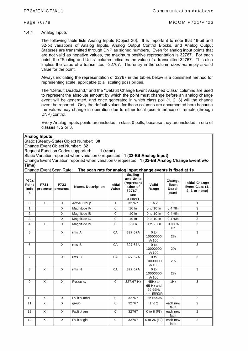
P72x/EN CT/A11 Communication database Page 76/78 MiCOM P721/P723 1.4.4 Analog Inputs
The following table lists Analog Inputs (Object 30). It is important to note that 16-bit and 32-bit variations of Analog Inputs, Analog Output Control Blocks, and Analog Output Statuses are transmitted through DNP as signed numbers. Even for analog input points that are not valid as negative values, the maximum positive representation is 32767. For each point, the “Scaling and Units” column indicates the value of a transmitted 32767. This also implies the value of a transmitted –32767. The entry in the column does not imply a valid value for the point.
Always indicating the representation of 32767 in the tables below is a consistent method for representing scale, applicable to all scaling possibilities.
The “Default Deadband,” and the “Default Change Event Assigned Class” columns are used to represent the absolute amount by which the point must change before an analog change event will be generated, and once generated in which class poll (1, 2, 3) will the change event be reported. Only the default values for these columns are documented here because the values may change in operation due to either local (user-interface) or remote (through DNP) control.
Every Analog Inputs points are included in class 0 polls, because they are included in one of classes 1, 2 or 3.
Analog Inputs Static (Steady-State) Object Number: 30 Change Event Object Number: 32 Request Function Codes supported: 1 (read) Static Variation reported when variation 0 requested: 1 (32-Bit Analog Input) Change Event Variation reported when variation 0 requested: 1 (32-Bit Analog Change Event w/o Time) Change Event Scan Rate: The scan rate for analog input change events is fixed at 1s
P72x Point Inde
x
P721 presence
P723 presence
Name/Description Initial Value
Scaling and Units (represent
ation of 32767 –
see above)
Valid Range
Change Event Dead- band
Initial Change Event Class (1, 2, 3 or none)
0 X X Active Group 1 32767 1 à 2 1 1
1 X Magnitude IA 0 10 In 0 to 10 In 0.4 %In 3
2 X Magnitude IB 0 10 In 0 to 10 In 0.4 %In 3
3 X Magnitude IC 0 10 In 0 to 10 In 0.4 %In 3
4 X X Magnitude IN 0 2 IEn 0 to 2 IEn 0.08 % IEn
3
5 X rms IA 0A 327.67A 0 to 10000000
A/100
2%
3
6 X rms IB 0A 327.67A 0 to 10000000
A/100
2%
3
7 X rms IC 0A 327.67A 0 to 10000000
A/100
2%
3
8 X X rms IN 0A 327.67A 0 to 10000000
A/100
2%
3
9 X X Frequency 0 327,67 Hz 45Hz to 65 Hz and 99.99Hz
== ERROR
1Hz 3
10 X X Fault number 0 32767 0 to 65535 1 2
11 X X group 0 32767 1 to 2 each new fault
2
12 X X Fault phase 0 32767 0 to 8 (F1) each new fault
2
13 X X Fault origin 0 32767 0 to 26 (F2) each new fault
2

Communication database P72x/EN CT/A11 MiCOM P721/P723 Page 77/78 Analog Inputs Static (Steady-State) Object Number: 30 Change Event Object Number: 32 Request Function Codes supported: 1 (read) Static Variation reported when variation 0 requested: 1 (32-Bit Analog Input) Change Event Variation reported when variation 0 requested: 1 (32-Bit Analog Change Event w/o Time) Change Event Scan Rate: The scan rate for analog input change events is fixed at 1s
P72x Point Inde
x
P721 presence
P723 presence
Name/Description Initial Value
Scaling and Units (represent
ation of 32767 –
see above)
Valid Range
Change Event Dead- band
Initial Change Event Class (1, 2, 3 or none)
14 X X Fault magnitude 0 10 In 0 to 10 In each new fault
2
15 X Fault magnitude IA 0 10 In 0 to 10 In each new fault
2
16 X Fault magnitude IB 0 10 In 0 to 10 In each new fault
2
17 X Fault magnitude IC 0 10 In 0 to 10 In each new fault
2
18 X X Fault magnitude IN 0 2 IEn 0 to 2 IEn each new fault
2
Format:
F1: 0: None, 1: Phase A, 2: Phase B, 3: Phase C, 4: Phase AB, 5: Phase AC, 6: Phase BC, 7: Phase A B C, 8: Earth.
F2: 0: Null, 1: Remote trip, 2: … (See format F78 in MODBUS conception document).

P72x/EN CT/A11 Communication database Page 78/78 MiCOM P721/P723
BLANK PAGE

Connection Diagrams P72x/EN CO/A11 MiCOM P721/P723
CONNECTION DIAGRAMS


Connection Diagrams P72x/EN CO/A11 MiCOM P721/P723 Page 1/2
BEFORE CARRYING OUT ANY WORK ON THE EQUIPMENT, THE USER SHOULD BE FAMILIAR WITH THE CONTENTS OF THE SAFETY GUIDE SFTY/4LM/G11-S OR LATER ISSUE, OR THE SAFETY AND TECHNICAL DATA SECTION OF THE TECHNICAL MANUAL AND ALSO THE RATINGS ON THE EQUIPMENT RATING LABEL."
CB
29
RS
485
Nota
:(1
)
(c)
(a)
(b)
30
32
*
31- +
34
P721
MiC
OM
26
28
24
22
L2
L1
RL4
RL2
RL3
RL1
20
1810 8 16
141224
33
+ -6
(d)
+ - + -
47
55
53
49
51
37 45
43
41
39
35
33
29
31
48
56
54
52
5038
46
44
4240
36
34
32
30
24
23
27
25
28
262
1 21
19
15
17
13
22
20
16
18
14
7 9 1153
8 12
1064
A
48
4756
55
WD
36
35
37
Phase
rota
tion
Auxili
ary
voltage
Pro
gra
mm
able
input
Pro
gra
mm
able
input
Case
eart
h
Module
term
inalblo
cks
vie
wed
from
pre
ar
(with
inte
gra
lcase
eart
hlin
k)
Watc
hdog
(4)
Pro
gra
mm
able
trip
pin
goutp
ut
Pro
gra
mm
able
outp
ut
Pro
gra
mm
able
outp
ut
Case
eart
hconnection
Port
com
munic
ation
(:Lin
kte
rmin
als
30
and
32
ifth
ere
lay
isconnecte
datth
eend
ofth
eR
S485
bus
)
CT
short
ing
links
make
befo
re(b
)
Short
term
inals
bre
ak
befo
re(c
)
Long
term
inals
Pin
ste
rmin
als
(pcb
type)
(2)
CT
connection
are
typic
alonly
(3)
Eart
hte
rmin
als
are
typic
alonly
(4)
The
MIC
OM
P120/P
121
rela
ys
are
show
nw
ith
supply
off.
*
CA B
5A
48
4756
1A
55
Altern
ative
:R
estr
icte
dE
art
hF
ault
Pro
tection
(Delta
connection)
CA B
P791
sta
bili
sin
gre
sis
tors
Altern
ative
:R
estr
icte
dE
art
hF
ault
Pro
tection
(S
tar
connection)
P791
(-V
)A
uxili
ary
voltage
Ctr
lshort
ing
rela
y
and
(c)
dis
connect
5A
1A
P791
(-V
)A
uxili
ary
voltage
Ctr
lshort
ing
rela
y
Auxili
ary
voltage
(+V
)
RS
t.R
St.
P3955ENa
{{ {
{{{{
SCHEME REPRESENTING MiCOM RELAY OFF

P72x/EN CO/A11 Connection Diagrams Page 2/2 MiCOM P721/P723
29
RS
48
5
Nota
:(1
)
(c)
(a)
(b)
30
32
*
31- +
34
P7
23
MiC
OM
33
+ -
Te
rre
bo
îtie
r
(d)
47
55
53
49
51
37 45
43
41
39
35
33
29
31
48
56
54
52
5038
46
44
4240
36
34
32
30
24
23
27
25
28
262
1 21
19
15
17
13
22
20
16
18
14
7 9 1153
8 12
1064
5A
5A
5A
5A
1A
1A
48
4746
45
44
43
4241
56
55
54
52 53
1A
1A
50
51
49
Altern
ative
:R
estr
icte
dE
art
hF
ault
Pro
tection
(S
tar
connection)
Au
xili
ary
vo
lta
ge
Thre
e-P
hase
Hig
hIm
pedance
Diffe
rential
Ca
se
ea
rth
Mo
du
lete
rmin
alb
locks
vie
we
dfr
om
pre
ar
(with
inte
gra
lca
se
ea
rth
link)
Ca
se
ea
rth
co
nn
ectio
n
Po
rtco
mm
un
ica
tio
n
(:
Lin
kte
rmin
als
30
an
d3
2if
the
rela
yis
co
nn
ecte
da
tth
ee
nd
of
the
RS
48
5b
us
)
CT
sh
ort
ing
links
ma
ke
be
fore
(b)
an
d(c
)d
isco
nn
ect
Sh
ort
term
ina
lsb
rea
kb
efo
re(c
)
Lo
ng
term
ina
ls
Pin
ste
rmin
als
(pcb
typ
e)
(2)
CT
co
nn
ectio
na
rety
pic
alo
nly
(3)
Ea
rth
term
ina
lsa
rety
pic
alo
nly
(4)
Th
eM
ICO
Mre
lays
are
sh
ow
nw
ith
su
pp
lyo
ff.
*
Altern
ative
:R
estr
icte
dE
art
hF
ault
Pro
tection
(Delta
connection)
L3
23
27
25
{{{{{{
21
19
L5
L4
26
17
28
24
22
L2
L1
+ - + - + - + - + -
Pro
gra
mm
ab
lein
pu
t
Pro
gra
mm
ab
lein
pu
t
Pro
gra
mm
ab
lein
pu
tinp
ut
Pro
gra
mm
ab
le
Pro
gra
mm
ab
lein
pu
t
RL
7
RL
8
13
15
11
{{{{{{{{
RL
6
RL
5
RL
4
RL
2
RL
3
RL
1
5 971320
1810 8 16
1412246
WD
36
35
37
Wa
tch
Do
g(4
)
Pro
gra
mm
ab
letr
ipp
ing
ou
tpu
t
Pro
gra
mm
ab
leo
utp
ut
Pro
gra
mm
ab
leo
utp
ut
Pro
gra
mm
ab
leo
utp
ut
Pro
gra
mm
ab
leo
utp
ut
Pro
gra
mm
ab
leo
utp
ut
Pro
gra
mm
ab
leo
utp
ut
CB
A
Ph
ase
rota
tio
n
P793
P7
91
an
dP
79
3sta
bili
sin
gre
sis
tors
(-V
)A
uxili
ary
vo
lta
ge
Ctr
lsh
ort
ing
rela
y
Au
xili
ary
vo
lta
ge
(+V
)
CA B
5A
48
5A
47
4645
44
5A
5A
43
42
41
56
1A
1A
55
54
53
52
1A
51
1A
50
49
P791
(-V
)A
uxili
ary
vo
lta
ge
Ctr
lsh
ort
ing
rela
y
CA B
5A
48
5A
47
4645
44
5A
5A
43
42
41
56
1A
1A
55
54
53
52
1A
51
1A
50
49
P791
(-V
)A
uxili
ary
vo
lta
ge
Ctr
lsh
ort
ing
rela
y
RS
t.
CT1
CT2
CTn
RS
t.
RS
t.
RS
t.
RS
t.
P3954ENa
SCHEME REPRESENTING MiCOM RELAY OFF

Commissioning Test & Record Sheets P72x/EN RS/A11 MiCOM P721/P723
COMMISSIONING TEST & RECORD SHEETS


Commissioning Test & Record Sheets P72x/EN RS/A11 MiCOM P721/P723 Page 1/22
CONTENTS
1. COMMISSIONING TEST SHEETS 3
1.1 Relay identification 3 1.2 Commissioning test record 3
2. COMMISSIONING SETTING RECORD SHEETS 6
2.1 OP PARAMETERS Menu 6 2.2 CONFIGURATION Menu 6 2.2.1 Connection menu 6 2.2.2 LEDs 5 to 8 configuration 7 2.2.3 Group select configuration 7 2.2.4 Alarms configuration 8 2.2.5 Inputs configuration 8 2.2.6 Relays maintenance 8 2.3 COMMUNICATION Menu 9 2.4 PROTECTION G1 Menu 10 2.4.1 [87N] Earth differential protection 10 2.4.2 [95N] Earth bus-wire supervision 10 2.4.3 [87] Phase differential protection (P723 only) 10 2.4.4 [95] Phase bus-wire supervision (P723 only) 11 2.5 PROTECTION G2 Menu 11 2.5.1 [87N] Earth differential protection 11 2.5.2 [95N] Earth bus-wire supervision 11 2.5.3 [87] Phase differential protection (P723 only) 12 2.5.4 [95] Phase bus-wire supervision (P723 only) 12 2.6 AUTOMAT.CTRL Menu 13 2.6.1 TRIP Command allocation 13 2.6.2 Latch function allocation 13 2.6.3 Blocking Logic 1 function allocation 14 2.6.4 Blocking Logic 1 function allocation 14 2.6.5 OUTPUT RELAYS allocation 14 2.6.6 LATCH OUTPUT RELAYS allocation 15 2.6.7 LOGIC INPUT allocation 16 2.6.8 CIRCUIT BREAKER FAILURE 16 2.6.9 LOGIC EQUATIONS 17 2.7 RECORDING Menu 21 2.7.1 FAULT RECORD Record 21 2.7.2 INSTANTANEOUS Record 21 2.7.3 DISTURBANCE RECORD 21

P72x/EN RS/A11 Commissioning Test & Record Sheets Page 2/22 MiCOM P721/P723
BLANK PAGE

Commissioning Test & Record Sheets P72x/EN RS/A11 MiCOM P721/P723 Page 3/22
1. COMMISSIONING TEST SHEETS
BEFORE CARRYING OUT ANY WORK ON THE EQUIPMENT, THE USER SHOULD BE FAMILIAR WITH THE CONTENTS OF THE SAFETY GUIDE SFTY/4LM/G11-S OR LATER ISSUE, OR THE SAFETY AND TECHNICAL DATA SECTION OF THE TECHNICAL MANUAL AND ALSO THE RATINGS ON THE EQUIPMENT RATING LABEL.
1.1 Relay identification
Commissioning date :
Engineer :
Substation :
Circuit :
Network nominal frequency:
MiCOM Overcurrent relay model : P721 P723
Serial number :
Rated current In :
Auxiliary voltage Uaux :
Communication protocol :
Language :
1.2 Commissioning test record
(put a cross after each checked stage)
Serial number check ?
All current transformer shorting switches closed ?
Wiring checked against diagram (if available) ?
Case earth installed ?
Test block connections checked (if installed) ?
Insulation tested ?

P72x/EN RS/A11 Commissioning Test & Record Sheets Page 4/22 MiCOM P721/P723
Auxiliary supply control
Auxiliary voltage to relay
Auxiliary voltage value ________________ Vdc/Vac Watchdog contacts
With auxiliary supply off Terminals 35 and 36
With auxiliary supply on Terminals 36 and 37
Measurements
Applied value Relay value
PHASE CT INPUT
Phase A current _______________ A A
Phase B current _______________ A A
Phase C current _______________ A A
EARTH CT INPUT
Earth current _______________ A A
Phase protection test
Theoretical value Relay value
Threshold I Diff _______________ A
I Diff Threshold A
I Diff drop Threshold A
Timer
Fault Timer tdiff at 2*I Diff ______________ ms A
Fault Timer tdiff at 10*I Diff ______________ ms A
Reset Timer tReset at 2*I Diff ______________ ms A
Reset Timer tReset at 10*I Diff ______________ ms A
Check Zone _______________ A
Reset Timer tReset ______________ ms A

Commissioning Test & Record Sheets P72x/EN RS/A11 MiCOM P721/P723 Page 5/22
Earth protection test
Theoretical value Relay value
Threshold Earth Diff _______________ A
I Diff Threshold A
I Diff drop Threshold A
Timer
Fault Timer tdiff at 2*I Diff ______________ ms A
Fault Timer tdiff at 10*I Diff ______________ ms A
Reset Timer tReset at 2*I Diff ______________ ms A
Reset Timer tReset at 10*I Diff ______________ ms A
Commissioning Engineer Date
_________________________ _______________

P72x/EN RS/A11 Commissioning Test & Record Sheets Page 6/22 MiCOM P721/P723
2. COMMISSIONING SETTING RECORD SHEETS 2.1 OP PARAMETERS Menu
Password :
Reference :
Software version :
Frequency : 50 Hz 60 Hz 2.2 CONFIGURATION Menu
2.2.1 Connection menu
Protection line select Earth Phase
Input Selection Current Voltage
If protection Line = Earth
E/Gnd Text N E G
Line CT Primary Ω
E/Gnd CT Primary Primary earth CT ratio
E/Gnd CT Secondary Secondary earth CT ratio 1 A 5 A
If protection Line = Phase
Phase A Text A L1 R
Phase B Text B L2 S
Phase C Text C L3 T
Stabiliz resist L1 (A, R) Ω
Stabiliz resist L2 (B, S) Ω
Stabiliz resist L3 (C, T) Ω
Line CT Primary Primary phase CT ratio
Line CT Secondary Secondary phase CT ratio 1 A 5 A

Commissioning Test & Record Sheets P72x/EN RS/A11 MiCOM P721/P723 Page 7/22 2.2.2 LEDs 5 to 8 configuration
• = available with this model.
LED 5 LED 6 LED 7 LED 8 Functions
P721
P723
Yes Yes Yes Yes
[87] Diff • [87N] Diff • • [87] tDiff • [87N] tDiff • • [87CZ] Check zone • [95] Sup • [95N] Sup • [95] tSup • [95N] tSup • • [95A] tSupA • [95B] tSupB • [95C] tSupC • Input 1 • • Input 2 • • Input 3 • Input 4 • Input 5 • tAux 1 • • tAux 2 • • tAux 3 • tAux 4 • tEqu.A • • tEqu.B • • tEqu.C • • tEqu.D • • tEqu.E • • tEqu.F • • tEqu.G • • tEqu.H • •
2.2.3 Group select configuration
Change group input Menu Input
Setting group 1 2

P72x/EN RS/A11 Commissioning Test & Record Sheets Page 8/22 MiCOM P721/P723 2.2.4 Alarms configuration
Inst. Self Reset? YES NO
Reset Led on fault YES NO
Alarm tAux1 YES NO
Alarm tAux2 YES NO
Alarm tAux3 (P723 only) YES NO
Alarm tAux4 (P723 only) YES NO
Alarm tAux5 (P723 only) YES NO
2.2.5 Inputs configuration
Inputs (P721 only) 2 1
Inputs (P723 only) 5 4 3 2 1
Voltage input DC DC AC
2.2.6 Relays maintenance
← P721 →
← P723 →
8 7 6 5 4 3 2 1 Fail Safe Relay
Maintenance Mode YES NO
← P721 →
← P723 →
8 7 6 5 W 4 3 2 1 Relays CMD

Commissioning Test & Record Sheets P72x/EN RS/A11 MiCOM P721/P723 Page 9/22 2.3 COMMUNICATION Menu
NOTE: Menu content depends on the communication protocol.
Communication ? YES NO Rear Comm. Address
Baud Rate 300 bds 600 bds 1.200 bds 2.400 bds 4.800 bds 9.600 bds 19.200 bds 38 400 bds Parity Odd Even None Data bits 7 8 Stop bits 1 2 Spont. Event. All IEC only None Command blocking YES NO Signal Blocking YES NO Measure Enabling ASDU 3.4&9 ASDU 9 ASDU 3.4 None Front Comm. Address
Date Format Private IEC

P72x/EN RS/A11 Commissioning Test & Record Sheets Page 10/22 MiCOM P721/P723 2.4 PROTECTION G1 Menu
2.4.1 [87N] Earth differential protection
[87N] Earth Diff protection? Yes No:
[87N] Threshold I diff= In
[87N] Threshold V diff= V
[87N] Flt Timer t Diff s
[87N] Flt Timer t Reset s
[87N] Measure Filter Sample mode
Fast sam-ple mode
Fourier mode
2.4.2 [95N] Earth bus-wire supervision
[95N] Earth bus-wire sup? Yes No: [95N] Threshold I Sup= In
[95N] Threshold V Sup= V
[95N] Flt Timer t Sup s
[95N] Flt Timer t Reset s
[95N] Measure Filter Sample mode
Fast sam-ple mode
Fourier mode
2.4.3 [87] Phase differential protection (P723 only)
[87] Phase Diff prot? Yes No: [87] Threshold I diff= In
[87] Threshold V diff= V
[87] Flt Timer t Diff s
[87] Check zone? Yes No: [87] Rst Timer t Reset s
[87] Measure Filter Sample mode
Fast sam-ple mode
Fourier mode
Commissioning Test & Record Sheets P72x/EN RS/A11 MiCOM P721/P723 Page 11/22 2.4.4 [95] Phase bus-wire supervision (P723 only)
[95] Phase bus-wire sup? Yes No: [95] Threshold I Sup= In
[95] Threshold V Sup= V
[95] Flt Timer t Sup s
[95] Flt Timer t Reset s
[95] Measure Filter Sample mode
Fast sam-ple mode
Fourier mode
2.5 PROTECTION G2 Menu
2.5.1 [87N] Earth differential protection
[87N] Earth Diff protection? Yes No:
[87N] Threshold I diff= In
[87N] Threshold V diff= V
[87N] Flt Timer t Diff s
[87N] Flt Timer t Reset s
[87N] Measure Filter Sample mode
Fast sam-ple mode
Fourier mode
2.5.2 [95N] Earth bus-wire supervision
[95N] Earth bus-wire sup? Yes No: [95N] Threshold I Sup= In
[95N] Threshold V Sup= V
[95N] Flt Timer t Sup s
[95N] Flt Timer t Reset s
[95N] Measure Filter Sample mode
Fast sam-ple mode
Fourier mode

P72x/EN RS/A11 Commissioning Test & Record Sheets Page 12/22 MiCOM P721/P723 2.5.3 [87] Phase differential protection (P723 only)
[87] Phase Diff prot? Yes No: [87] Threshold I diff= In
[87] Threshold V diff= V
[87] Flt Timer t Diff s
[87] Check zone? Yes No: [87] Rst Timer t Reset s
[87] Measure Filter Sample mode
Fast sam-ple mode
Fourier mode
2.5.4 [95] Phase bus-wire supervision (P723 only)
[95] Phase bus-wire sup? Yes No: [95] Threshold I Sup= In
[95] Threshold V Sup= V
[95] Flt Timer t Sup s
[95] Flt Timer t Reset s
[95] Measure Filter Sample mode
Fast sam-ple mode
Fourier mode

Commissioning Test & Record Sheets P72x/EN RS/A11 MiCOM P721/P723 Page 13/22 2.6 AUTOMAT.CTRL Menu
2.6.1 TRIP Command allocation
P721 P723 Function
Yes Yes
Trip [87] tDiff
Trip [87N] tDiff
Trip tAux 1
Trip tAux 2
Trip tAux 3
Trip tAux 4
Control Trip
Trip Equ A
Trip Equ B
Trip Equ C
Trip Equ D
Trip Equ E
Trip Equ F
Trip Equ G
Trip Equ H
2.6.2 Latch function allocation
P721 P723 Function
YES YES
Latch [87N] tDiff
Latch [87] tDiff
Latch t Aux 1
Latch t Aux 2
Latch t Aux 3
Latch t Aux 4
Latch Control Trip
Latch tEqu.A
Latch tEqu.B
Latch tEqu.C
Latch tEqu.D
Latch tEqu.E
Latch tEqu.F
Latch tEqu.G
Latch tEqu.H

P72x/EN RS/A11 Commissioning Test & Record Sheets Page 14/22 MiCOM P721/P723 2.6.3 Blocking Logic 1 function allocation
P721 P723 Function
Yes Yes
[87N] tDiff
[87] tDiff
tAux 1
tAux 2
tAux 3
tAux 4
2.6.4 Blocking Logic 1 function allocation
P721 P723 Function
Yes Yes
[87N] tDiff
[87] tDiff
tAux 1
tAux 2
tAux 3
tAux 4
2.6.5 OUTPUT RELAYS allocation
← P721 →
← P723 →
RL2 RL3 RL4 RL5 RL6 RL7 RL8 Function
P721
P723
Yes Yes Yes Yes Yes Yes Yes
[87N] Diff • • [87N] tDiff • • [87] Diff • [87] tDiff • [87CZ] ChkZone • [95N] Sup • • [95N] tSup • • [95] Sup • [95] tSup • Buswire Short • • [95A] tSup A • [95B] tSup B • [95C] tSup C •
Commissioning Test & Record Sheets P72x/EN RS/A11 MiCOM P721/P723 Page 15/22
← P721 →
← P723 →
RL2 RL3 RL4 RL5 RL6 RL7 RL8 Function
P721
P723
Yes Yes Yes Yes Yes Yes Yes
CB Fail • • t Aux 1 • • t Aux 2 • • t Aux 3 • t Aux 4 • Active group • • Control trip • • Input1 • • Input2 • • Input3 • Input4 • Input5 • tEqu. A • • tEqu. B • • tEqu. C • • tEqu D • • tEqu E • • tEqu. F • • tEqu. G • • tEqu. H • •
2.6.6 LATCH OUTPUT RELAYS allocation
Output 2 YES NO Output 3 YES NO Output 4 YES NO Output 5 (P723) YES NO Output 6 (P723) YES NO Output 7 (P723) YES NO Output 8 (P723) YES NO

P72x/EN RS/A11 Commissioning Test & Record Sheets Page 16/22 MiCOM P721/P723 2.6.7 LOGIC INPUT allocation
2.6.7.1 Inputs
Inputs Function
P120
P123
1 2 3 4 5
Unlatch • • Aux 1 • • Aux 2 • • Aux 3 • Aux 4 • Block Logic 2 • • Start Disturb • • Start Block Logic 1 • • Start Block Logic 2 • • Change setting • • Reset Leds • • Maint. Mode • • Local Mode • • Synchro • • [87CZ] Chk Zone •
2.6.7.2 tAux
Aux 1 : Time tAux 1 s
Aux 2 : Time tAux 2 s
Aux 3 : Time tAux 3 (P723) s
Aux 5 : Time tAux 4 (P723) s
2.6.8 CIRCUIT BREAKER FAILURE
CB Fail ? YES NO
t Diff < = In
V Diff < = V
CB Fail Time tBF ms

Commissioning Test & Record Sheets P72x/EN RS/A11 MiCOM P721/P723 Page 17/22 2.6.9 LOGIC EQUATIONS
Equ. A Boolean Logic
A.00 = / = NOT
A.01 OR / = OR NOT / AND / = AND NOT
A.02 OR / = OR NOT / AND / = AND NOT
A.03 OR / = OR NOT / AND / = AND NOT
A.04 OR / = OR NOT / AND / = AND NOT
A.05 OR / = OR NOT / AND / = AND NOT
A.06 OR / = OR NOT / AND / = AND NOT
A.07 OR / = OR NOT / AND / = AND NOT
A.08 OR / = OR NOT / AND / = AND NOT
A.09 OR / = OR NOT / AND / = AND NOT
A.10 OR / = OR NOT / AND / = AND NOT
A.11 OR / = OR NOT / AND / = AND NOT
A.12 OR / = OR NOT / AND / = AND NOT
A.13 OR / = OR NOT / AND / = AND NOT
A.14 OR / = OR NOT / AND / = AND NOT
A.15 OR / = OR NOT / AND / = AND NOT
T Operate ms
T Reset ms
Equ B Boolean Logic
B.00 = / = NOT
B.01 OR / = OR NOT / AND / = AND NOT
B.02 OR / = OR NOT / AND / = AND NOT
B.03 OR / = OR NOT / AND / = AND NOT
B.04 OR / = OR NOT / AND / = AND NOT
B.05 OR / = OR NOT / AND / = AND NOT
B.06 OR / = OR NOT / AND / = AND NOT
B.07 OR / = OR NOT / AND / = AND NOT
B.08 OR / = OR NOT / AND / = AND NOT
B.09 OR / = OR NOT / AND / = AND NOT
B.10 OR / = OR NOT / AND / = AND NOT
B.11 OR / = OR NOT / AND / = AND NOT
B.12 OR / = OR NOT / AND / = AND NOT
B.13 OR / = OR NOT / AND / = AND NOT
B.14 OR / = OR NOT / AND / = AND NOT
B.15 OR / = OR NOT / AND / = AND NOT
T Operate ms
T Reset ms

P72x/EN RS/A11 Commissioning Test & Record Sheets Page 18/22 MiCOM P721/P723
Equ. C Boolean Logic
C.00 = / = NOT
C.01 OR / = OR NOT / AND / = AND NOT
C.02 OR / = OR NOT / AND / = AND NOT
C.03 OR / = OR NOT / AND / = AND NOT
C.04 OR / = OR NOT / AND / = AND NOT
C.05 OR / = OR NOT / AND / = AND NOT
C.06 OR / = OR NOT / AND / = AND NOT
C.07 OR / = OR NOT / AND / = AND NOT
C.08 OR / = OR NOT / AND / = AND NOT
C.09 OR / = OR NOT / AND / = AND NOT
C.10 OR / = OR NOT / AND / = AND NOT
C.11 OR / = OR NOT / AND / = AND NOT
C.12 OR / = OR NOT / AND / = AND NOT
C.13 OR / = OR NOT / AND / = AND NOT
C.14 OR / = OR NOT / AND / = AND NOT
C.15 OR / = OR NOT / AND / = AND NOT
T Operate ms
T Reset ms
Equ. D Boolean Logic
D.00 = / = NOT
D.01 OR / = OR NOT / AND / = AND NOT
D.02 OR / = OR NOT / AND / = AND NOT
D.03 OR / = OR NOT / AND / = AND NOT
D.04 OR / = OR NOT / AND / = AND NOT
D.05 OR / = OR NOT / AND / = AND NOT
D.06 OR / = OR NOT / AND / = AND NOT
D.07 OR / = OR NOT / AND / = AND NOT
D.08 OR / = OR NOT / AND / = AND NOT
D.09 OR / = OR NOT / AND / = AND NOT
D.10 OR / = OR NOT / AND / = AND NOT
D.11 OR / = OR NOT / AND / = AND NOT
D.12 OR / = OR NOT / AND / = AND NOT
D.13 OR / = OR NOT / AND / = AND NOT
D.14 OR / = OR NOT / AND / = AND NOT
D.15 OR / = OR NOT / AND / = AND NOT
T Operate ms
T Reset ms

Commissioning Test & Record Sheets P72x/EN RS/A11 MiCOM P721/P723 Page 19/22
Equ. E Boolean Logic
E.00 = / = NOT
E.01 OR / = OR NOT / AND / = AND NOT
E.02 OR / = OR NOT / AND / = AND NOT
E.03 OR / = OR NOT / AND / = AND NOT
E.04 OR / = OR NOT / AND / = AND NOT
E.05 OR / = OR NOT / AND / = AND NOT
E.06 OR / = OR NOT / AND / = AND NOT
E.07 OR / = OR NOT / AND / = AND NOT
E.08 OR / = OR NOT / AND / = AND NOT
E.09 OR / = OR NOT / AND / = AND NOT
E.10 OR / = OR NOT / AND / = AND NOT
E.11 OR / = OR NOT / AND / = AND NOT
E.12 OR / = OR NOT / AND / = AND NOT
E.13 OR / = OR NOT / AND / = AND NOT
E.14 OR / = OR NOT / AND / = AND NOT
E.15 OR / = OR NOT / AND / = AND NOT
T Operate ms
T Reset ms
Equ. F Boolean Logic
F.00 = / = NOT
F.01 OR / = OR NOT / AND / = AND NOT
F.02 OR / = OR NOT / AND / = AND NOT
F.03 OR / = OR NOT / AND / = AND NOT
F.04 OR / = OR NOT / AND / = AND NOT
F.05 OR / = OR NOT / AND / = AND NOT
F.06 OR / = OR NOT / AND / = AND NOT
F.07 OR / = OR NOT / AND / = AND NOT
F.08 OR / = OR NOT / AND / = AND NOT
F.09 OR / = OR NOT / AND / = AND NOT
F.10 OR / = OR NOT / AND / = AND NOT
F.11 OR / = OR NOT / AND / = AND NOT
F.12 OR / = OR NOT / AND / = AND NOT
F.13 OR / = OR NOT / AND / = AND NOT
F.14 OR / = OR NOT / AND / = AND NOT
F.15 OR / = OR NOT / AND / = AND NOT
T Operate ms
T Reset ms

P72x/EN RS/A11 Commissioning Test & Record Sheets Page 20/22 MiCOM P721/P723
Equ. G Boolean Logic
G.00 = / = NOT
G.01 OR / = OR NOT / AND / = AND NOT
G.02 OR / = OR NOT / AND / = AND NOT
G.03 OR / = OR NOT / AND / = AND NOT
G.04 OR / = OR NOT / AND / = AND NOT
G.05 OR / = OR NOT / AND / = AND NOT
G.06 OR / = OR NOT / AND / = AND NOT
G.07 OR / = OR NOT / AND / = AND NOT
G.08 OR / = OR NOT / AND / = AND NOT
G.09 OR / = OR NOT / AND / = AND NOT
G.10 OR / = OR NOT / AND / = AND NOT
G.11 OR / = OR NOT / AND / = AND NOT
G.12 OR / = OR NOT / AND / = AND NOT
G.13 OR / = OR NOT / AND / = AND NOT
G.14 OR / = OR NOT / AND / = AND NOT
G.15 OR / = OR NOT / AND / = AND NOT
T Operate ms
T Reset ms
Equ. H Boolean Logic
H.00 = / = NOT
H.01 OR / = OR NOT / AND / = AND NOT
H.02 OR / = OR NOT / AND / = AND NOT
H.03 OR / = OR NOT / AND / = AND NOT
H.04 OR / = OR NOT / AND / = AND NOT
H.05 OR / = OR NOT / AND / = AND NOT
H.06 OR / = OR NOT / AND / = AND NOT
H.07 OR / = OR NOT / AND / = AND NOT
H.08 OR / = OR NOT / AND / = AND NOT
H.09 OR / = OR NOT / AND / = AND NOT
H.10 OR / = OR NOT / AND / = AND NOT
H.11 OR / = OR NOT / AND / = AND NOT
H.12 OR / = OR NOT / AND / = AND NOT
H.13 OR / = OR NOT / AND / = AND NOT
H.14 OR / = OR NOT / AND / = AND NOT
H.15 OR / = OR NOT / AND / = AND NOT
T Operate ms
T Reset ms

Commissioning Test & Record Sheets P72x/EN RS/A11 MiCOM P721/P723 Page 21/22 2.7 RECORDING Menu
2.7.1 FAULT RECORD Record
Fault Record
Fault Time : :
Fault date / /
Active Set Group 1 2
Faulted phase None Phase A Phase B Phase C Earth
Threshold
Fault Magnitude A
IA Diff R.M.S A
IB Diff R.M.S A
IC Diff R.M.S A
IN Diff R.M.S A
2.7.2 INSTANTANEOUS Record
Number 1 2 3 4 5
Hour : : :
Date / /
Origin
Length s
Trip YES NO
2.7.3 DISTURBANCE RECORD
Pre-time ms
Post-time ms
Disturb Rec Trig ON INST. ON TRIP

P72x/EN RS/A11 Commissioning Test & Record Sheets Page 22/22 MiCOM P721/P723
BLANK PAGE

Hardware/Software Version P72x/EN VC/B21 History and Compatibility MiCOM P721/P723
HARDWARE VERSION HISTORY AND
COMPATIBILITY


Hardware/Software Version P72x/EN VC/B21 History and Compatibility MiCOM P721/P723 Page 1/4
CONTENTS
1. MiCOM P721 3
2. MiCOM P723 4

P72x/EN VC/B21 Hardware/Software Version History and Compatibility Page 2/4 MiCOM P721/P723
BLANK PAGE

Hardware/Software Version P72x/EN VC/B21 History and Compatibility MiCOM P721/P723 Page 3/4
1. MiCOM P721
Relay Type P721
Software Version
Date of Issue Full Description of Changes
S1 Compati-bility
Backward Compatibility with previous hardware
V11.B 03/2009 V11.B software the first software for the P721 hardware (first issue)
V2.14 V3.0
HARD 5
V11.D 12/2011 New Schneider Electric Brand V3.4 HARD 5

P72x/EN VC/B21 Hardware/Software Version History and Compatibility Page 4/4 MiCOM P721/P723
2. MiCOM P723
Relay Type P723
Software Version
Date of Issue Full Description of Changes
S1 Compati-bility
Backward Compatibility with previous hardware
V11.B 03/2009 V11.B software is the first software for the P723 hardware (first issue)
V2.14 V3.0
HARD 5
V11.D 12/2011 New Schneider Electric Brand V3.4 HARD 5


©
201
2 S
chne
ider
Ele
ctric
. All
right
s re
serv
ed.
Schneider Electric 35 rue Joseph Monier 92506 Rueil-Malmaison FRANCE
Phone: +33 (0) 1 41 29 70 00 Fax: +33 (0) 1 41 29 71 00 www.schneider-electric.com Publishing: Schneider Electric
Publication: P72x/EN T/B21 01/2012