Embed Size (px)
Citation preview
GE Grid Solutions
MiCOM P40 Agile P241, P242, P243
Technical Manual Rotating Machine Protection Relay
Hardware version: J (P241), K (P242/3) Software version: 60 Publication reference: P24x/EN M/I72

CONTENTS
Safety Section P24x/EN SS/I72
Section 1 Introduction P24x/EN IT/I72
Section 2 Technical Data P24x/EN TD/I72
Section 3 Getting Started P24x/EN GS/I72
Section 4 Settings P24x/EN ST/I72
Section 5 Operation P24x/EN OP/I72
Section 6 Application Notes P24x/EN AP/I72
Section 7 Programmable Logic P24x/EN PL/I72
Section 8 Measurements and Recording P24x/EN MR/I72
Section 9 Firmware Design P24x/EN FD/I72
Section 10 Commissioning P24x/EN CM/I72
Section 11 Maintenance P24x/EN MT/I72
Section 12 Troubleshooting P24x/EN TS/I72
Section 13 SCADA Communications P24x/EN SC/I72
Section 14 Symbols and Glossary P24x/EN SG/I72
Section 15 Installation P24x/EN IN/I72
Section 16 Firmware and Service Manual Version History P24x/EN VH/I72
SS
IT
TD
GS
ST
OP
AP
PL
MR
FD
CM
MT
TS
SC
SG
VH
IN


Safety Section
P24x/EN SS/I72
SS
SAFETY SECTION

P24x/EN SS/I72
Safety Section
SS
Safety Section
P24x/EN SS/I72 (SS) - 1
SS
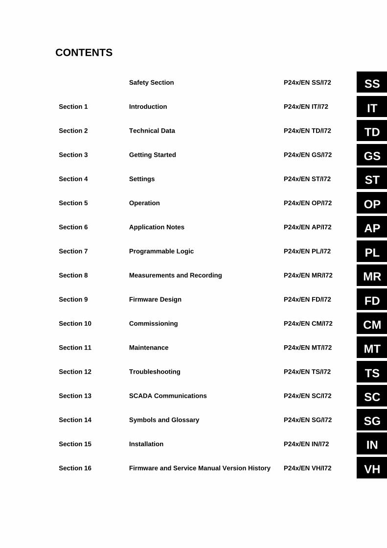
CONTENTS 1. OVERVIEW 3
2. HEALTH AND SAFETY 4
3. SYMBOLS 5
4. INSTALLING, COMMISSIONING AND SERVICING 6
4.1 Lifting Hazards 6
4.2 Electrical Hazards 6
5. DECOMMISSIONING AND DISPOSAL 12
6. REGULATORY COMPLIANCE 13
6.1 EMC Compliance: 2014/30/EU 13
6.2 LVD Compliance: 2014/35/EU 13
6.3 R&TTE Compliance: 2014/53/EU 13
6.4 UL/CUL Compliance 13
6.5 ATEX Compliance: 2014/34/EU 13

P24x/EN SS/I72
Safety Section (SS) - 2
SS

Safety Section
P24x/EN SS/I72 (SS) - 3
SS
1. OVERVIEW This chapter provides information about the safe handling of the equipment. The equipment must be properly installed and handled in order to maintain it in a safe condition and to keep personnel safe at all times. You must be familiar with information contained in this chapter before unpacking, installing, commissioning, or servicing the equipment.

P24x/EN SS/I72
Safety Section (SS) - 4
SS
2. HEALTH AND SAFETY Personnel associated with the equipment must be familiar with the contents of this Safety Information.
When electrical equipment is in operation, dangerous voltages are present in certain parts of the equipment. Improper use of the equipment and failure to observe warning notices will endanger personnel.
Only qualified personnel may work on or operate the equipment. Qualified personnel are individuals who are:
• familiar with the installation, commissioning, and operation of the equipment and the system to which it is being connected.
• familiar with accepted safety engineering practises and are authorised to energise and de-energise equipment in the correct manner.
• trained in the care and use of safety apparatus in accordance with safety engineering practises
• trained in emergency procedures (first aid).
The documentation provides instructions for installing, commissioning and operating the equipment. It cannot, however cover all conceivable circumstances. In the event of questions or problems, do not take any action without proper authorisation. Please contact your local sales office and request the necessary information.

Safety Section
P24x/EN SS/I72 (SS) - 5
SS
3. SYMBOLS Throughout this manual you will come across the following symbols. You will also see these symbols on parts of the equipment.
Refer to equipment documentation. Failure to do so could result in damage to the equipment
Risk of electric shock
Risk of damage to eyesight
Earth terminal. Note: This symbol may also be used for a protective conductor (earth) terminal if that terminal is part of a terminal block or sub-assembly.
Protective conductor (earth) terminal
Instructions on disposal requirements
The term 'Earth' used in this manual is the direct equivalent of the North American term 'Ground'.
P24x/EN SS/I72
Safety Section (SS) - 6
SS
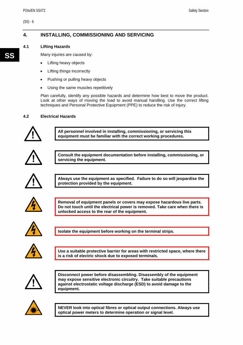
4. INSTALLING, COMMISSIONING AND SERVICING
4.1 Lifting Hazards
Many injuries are caused by:
• Lifting heavy objects
• Lifting things incorrectly
• Pushing or pulling heavy objects
• Using the same muscles repetitively
Plan carefully, identify any possible hazards and determine how best to move the product. Look at other ways of moving the load to avoid manual handling. Use the correct lifting techniques and Personal Protective Equipment (PPE) to reduce the risk of injury.
4.2 Electrical Hazards
All personnel involved in installing, commissioning, or servicing this equipment must be familiar with the correct working procedures.
Consult the equipment documentation before installing, commissioning, or servicing the equipment.
Always use the equipment as specified. Failure to do so will jeopardise the protection provided by the equipment.
Removal of equipment panels or covers may expose hazardous live parts. Do not touch until the electrical power is removed. Take care when there is unlocked access to the rear of the equipment.
Isolate the equipment before working on the terminal strips.
Use a suitable protective barrier for areas with restricted space, where there is a risk of electric shock due to exposed terminals.
Disconnect power before disassembling. Disassembly of the equipment may expose sensitive electronic circuitry. Take suitable precautions against electrostatic voltage discharge (ESD) to avoid damage to the equipment.
NEVER look into optical fibres or optical output connections. Always use optical power meters to determine operation or signal level.
Safety Section
P24x/EN SS/I72 (SS) - 7
SS
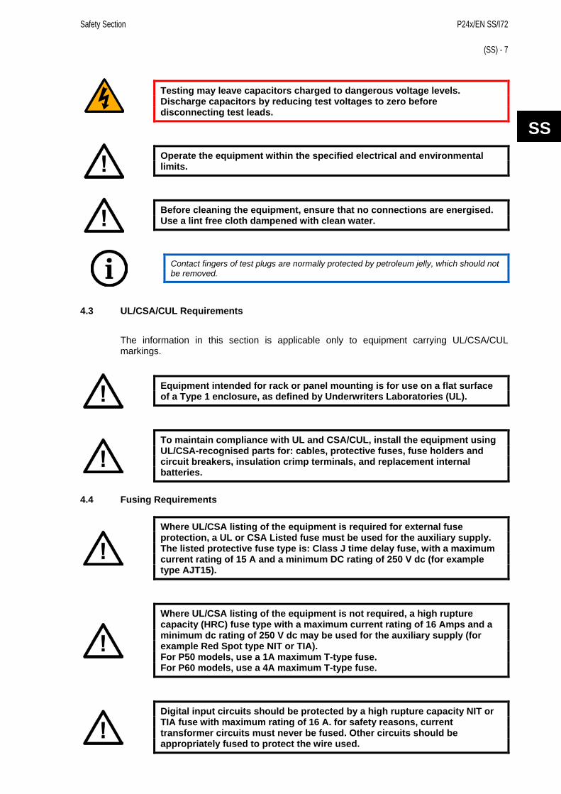
Testing may leave capacitors charged to dangerous voltage levels. Discharge capacitors by reducing test voltages to zero before disconnecting test leads.
Operate the equipment within the specified electrical and environmental limits.
Before cleaning the equipment, ensure that no connections are energised. Use a lint free cloth dampened with clean water.
Contact fingers of test plugs are normally protected by petroleum jelly, which should not be removed.
4.3 UL/CSA/CUL Requirements
The information in this section is applicable only to equipment carrying UL/CSA/CUL markings.
Equipment intended for rack or panel mounting is for use on a flat surface of a Type 1 enclosure, as defined by Underwriters Laboratories (UL).
To maintain compliance with UL and CSA/CUL, install the equipment using UL/CSA-recognised parts for: cables, protective fuses, fuse holders and circuit breakers, insulation crimp terminals, and replacement internal batteries.
4.4 Fusing Requirements
Where UL/CSA listing of the equipment is required for external fuse protection, a UL or CSA Listed fuse must be used for the auxiliary supply. The listed protective fuse type is: Class J time delay fuse, with a maximum current rating of 15 A and a minimum DC rating of 250 V dc (for example type AJT15).
Where UL/CSA listing of the equipment is not required, a high rupture capacity (HRC) fuse type with a maximum current rating of 16 Amps and a minimum dc rating of 250 V dc may be used for the auxiliary supply (for example Red Spot type NIT or TIA). For P50 models, use a 1A maximum T-type fuse. For P60 models, use a 4A maximum T-type fuse.
Digital input circuits should be protected by a high rupture capacity NIT or TIA fuse with maximum rating of 16 A. for safety reasons, current transformer circuits must never be fused. Other circuits should be appropriately fused to protect the wire used.
P24x/EN SS/I72
Safety Section (SS) - 8
SS
CTs must NOT be fused since open circuiting them may produce lethal hazardous voltages
4.5 Equipment Connections
Terminals exposed during installation, commissioning and maintenance may present a hazardous voltage unless the equipment is electrically isolated.
Tighten M4 clamping screws of heavy duty terminal block connectors to a nominal torque of 1.3 Nm. Tighten captive screws of terminal blocks to 0.5 Nm minimum and 0.6 Nm maximum.
Always use insulated crimp terminations for voltage and current connections.
Always use the correct crimp terminal and tool according to the wire size.
Watchdog (self-monitoring) contacts are provided to indicate the health of the device on some products. We strongly recommend that you hard wire these contacts into the substation's automation system, for alarm purposes.
4.6 Protection Class 1 Equipment Requirements
Earth the equipment with the supplied PCT (Protective Conductor Terminal).
Do not remove the PCT.
The PCT is sometimes used to terminate cable screens. Always check the PCT’s integrity after adding or removing such earth connections.
Use a locknut or similar mechanism to ensure the integrity of stud-connected PCTs.
Safety Section
P24x/EN SS/I72 (SS) - 9
SS
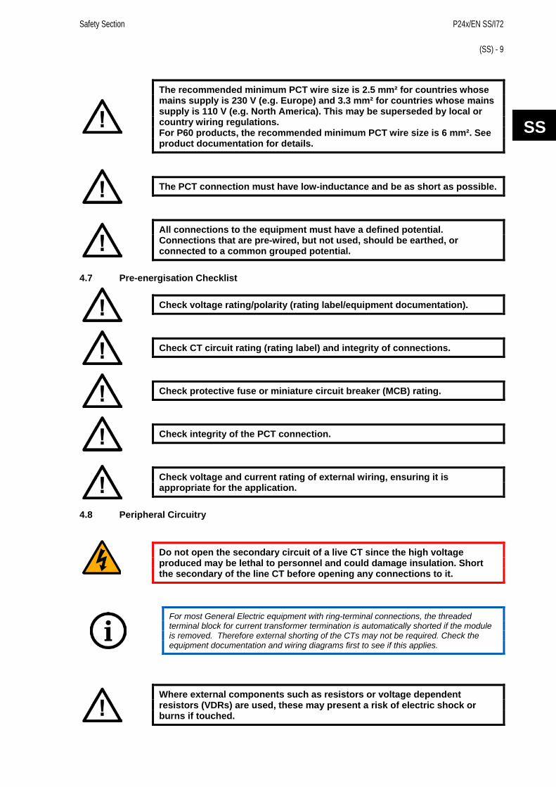
The recommended minimum PCT wire size is 2.5 mm² for countries whose mains supply is 230 V (e.g. Europe) and 3.3 mm² for countries whose mains supply is 110 V (e.g. North America). This may be superseded by local or country wiring regulations. For P60 products, the recommended minimum PCT wire size is 6 mm². See product documentation for details.
The PCT connection must have low-inductance and be as short as possible.
All connections to the equipment must have a defined potential. Connections that are pre-wired, but not used, should be earthed, or connected to a common grouped potential.
4.7 Pre-energisation Checklist
Check voltage rating/polarity (rating label/equipment documentation).
Check CT circuit rating (rating label) and integrity of connections.
Check protective fuse or miniature circuit breaker (MCB) rating.
Check integrity of the PCT connection.
Check voltage and current rating of external wiring, ensuring it is appropriate for the application.
4.8 Peripheral Circuitry
Do not open the secondary circuit of a live CT since the high voltage produced may be lethal to personnel and could damage insulation. Short the secondary of the line CT before opening any connections to it.
For most General Electric equipment with ring-terminal connections, the threaded terminal block for current transformer termination is automatically shorted if the module is removed. Therefore external shorting of the CTs may not be required. Check the equipment documentation and wiring diagrams first to see if this applies.
Where external components such as resistors or voltage dependent resistors (VDRs) are used, these may present a risk of electric shock or burns if touched.
P24x/EN SS/I72
Safety Section (SS) - 10
SS
Take extreme care when using external test blocks and test plugs such as the MMLG, MMLB and P990, as hazardous voltages may be exposed. Ensure that CT shorting links are in place before removing test plugs, to avoid potentially lethal voltages.
Data communication cables with accessible screens and/or screen conductors, (including optical fibre cables with metallic elements), may create an electric shock hazard in a sub-station environment if both ends of the cable screen are not connected to the same equipotential bonded earthing system. To reduce the risk of electric shock due to transferred potential hazards: i. The installation shall include all necessary protection measures to ensure that no fault currents can flow in the connected cable screen conductor. ii. The connected cable shall have its screen conductor connected to the protective conductor terminal (PCT) of the connected equipment at both ends. This connection may be inherent in the connectors provided on the equipment but, if there is any doubt, this must be confirmed by a continuity test. iii. The protective conductor terminal (PCT) of each piece of connected equipment shall be connected directly to the same equipotential bonded earthing system. iv. If, for any reason, both ends of the cable screen are not connected to the same equipotential bonded earth system, precautions must be taken to ensure that such screen connections are made safe before work is done to, or in proximity to, any such cables. v. No equipment shall be connected to any download or maintenance circuits or connectors of this product except temporarily and for maintenance purposes only. vi. Equipment temporarily connected to this product for maintenance purposes shall be protectively earthed (if the temporary equipment is required to be protectively earthed), directly to the same equipotential bonded earthing system as the product.
Small Form-factor Pluggable (SFP) modules which provide copper Ethernet connections typically do not provide any additional safety isolation. Copper Ethernet SFP modules must only be used in connector positions intended for this type of connection.
4.9 Upgrading/Servicing
Do not insert or withdraw modules, PCBs or expansion boards from the equipment while energised, as this may result in damage to the equipment. Hazardous live voltages would also be exposed, endangering personnel.
Internal modules and assemblies can be heavy and may have sharp edges. Take care when inserting or removing modules into or out of the IED.

Safety Section
P24x/EN SS/I72 (SS) - 11
SS
P24x/EN SS/I72
Safety Section (SS) - 12
SS
5. DECOMMISSIONING AND DISPOSAL
Before decommissioning, completely isolate the equipment power supplies (both poles of any dc supply). The auxiliary supply input may have capacitors in parallel, which may still be charged. To avoid electric shock, discharge the capacitors using the external terminals before decommissioning.
Avoid incineration or disposal to water courses. Dispose of the equipment in a safe, responsible and environmentally friendly manner, and if applicable, in accordance with country-specific regulations.
Safety Section
P24x/EN SS/I72 (SS) - 13
SS
6. REGULATORY COMPLIANCE Compliance with the European Commission Directive on EMC and LVD is demonstrated using a technical file.
6.1 EMC Compliance: 2014/30/EU
The product specific Declaration of Conformity (DoC) lists the relevant harmonised standard(s) or conformity assessment used to demonstrate compliance with the EMC directive.
6.2 LVD Compliance: 2014/35/EU
The product specific Declaration of Conformity (DoC) lists the relevant harmonized standard(s) or conformity assessment used to demonstrate compliance with the LVD directive.
Safety related information, such as the installation I overvoltage category, pollution degree and operating temperature ranges are specified in the Technical Data section of the relevant product documentation and/or on the product labelling.
Unless otherwise stated in the Technical Data section of the relevant product documentation, the equipment is intended for indoor use only. Where the equipment is required for use in an outdoor location, it must be mounted in a specific cabinet or housing to provide the equipment with the appropriate level of protection from the expected outdoor environment.
6.3 R&TTE Compliance: 2014/53/EU
Radio and Telecommunications Terminal Equipment (R&TTE) directive 2014/53/EU.
Conformity is demonstrated by compliance to both the EMC directive and the Low Voltage directive, to zero volts.
6.4 UL/CUL Compliance
If marked with this logo, the product is compliant with the requirements of the Canadian and USA Underwriters Laboratories.
The relevant UL file number and ID is shown on the equipment.
6.5 ATEX Compliance: 2014/34/EU
Products marked with the 'explosion protection' Ex symbol (shown in the example, below) are compliant with the ATEX directive. The product specific Declaration of Conformity (DoC) lists the Notified Body, Type Examination Certificate, and relevant harmonized standard or conformity assessment used to demonstrate compliance with the ATEX directive.
The ATEX Equipment Protection level, Equipment group, and Zone definition will be marked on the
product.
For example:

P24x/EN SS/I72
Safety Section (SS) - 14
SS
Where:
'II' Equipment Group: Industrial.
'(2)G' High protection equipment category, for control of equipment in gas atmospheres in Zone 1 and 2. This equipment (with parentheses marking around the zone number) is not itself suitable for operation within a potentially explosive atmosphere.

Safety Section
P24x/EN SS/I72 (SS) - 15
SS

Introduction
P24x/EN IT/I72 MiCOM P40 Agile P241, P242, P243 (IT) 1-1
IT
INTRODUCTION

P24x/EN IT/I72
Introduction (IT)1-2 MiCOM P40 Agile P241, P242, P243
IT
Introduction
P24x/EN IT/I72 MiCOM P40 Agile P241, P242, P243 (IT) 1-3
IT
CONTENTS
1 MICOM DOCUMENTATION STRUCTURE 5
2 INTRODUCTION TO MICOM 7
3 PRODUCT SCOPE 8 3.1 Functional overview 8 3.2 Ordering options 12
FIGURES Figure 1: Functional diagram 11
TABLES Table 1: Functional overview 10

P24x/EN IT/I72
Introduction (IT)1-4 MiCOM P40 Agile P241, P242, P243
IT
Introduction
P24x/EN IT/I72 MiCOM P40 Agile P241, P242, P243 (IT) 1-5
IT
1 MICOM DOCUMENTATION STRUCTURE The manual provides a functional and technical description of the MiCOM protection relay and a comprehensive set of instructions for the relay’s use and application.
The chapter contents are summarized below:
P24x/EN IT Introduction A guide to the MiCOM range of relays and the documentation structure. General safety aspects of handling Electronic Equipment are discussed with particular reference to relay safety symbols. Also a general functional overview of the relay and brief application summary is given.
P24x/EN TD Technical Data Technical data including setting ranges, accuracy limits, recommended operating conditions, ratings and performance data. Compliance with norms and international standards is quoted where appropriate.
P24x/EN GS Getting Started A guide to the different user interfaces of the protection relay describing how to start using it. This chapter provides detailed information regarding the communication interfaces of the relay, including a detailed description of how to access the settings database stored within the relay.
P24x/EN ST Settings List of all relay settings, including ranges, step sizes and defaults, together with a brief explanation of each setting.
P24x/EN OP Operation A comprehensive and detailed functional description of all protection and non-protection functions.
P24x/EN AP Application Notes This chapter includes a description of common power system applications of the relay, calculation of suitable settings, some typical worked examples, and how to apply the settings to the relay.
P24x/EN PL Programmable Logic Overview of the programmable scheme logic and a description of each logical node. This chapter includes the factory default (PSL) and an explanation of typical applications.
P24x/EN MR Measurements and Recording Detailed description of the relays recording and measurements functions including the configuration of the event and disturbance recorder and measurement functions.
P24x/EN FD Firmware Design Overview of the operation of the relay’s hardware and software. This chapter includes information on the self-checking features and diagnostics of the relay.
P24x/EN CM Commissioning Instructions on how to commission the relay, comprising checks on the calibration and functionality of the relay.
P24x/EN MT Maintenance A general maintenance policy for the relay is outlined.
P24x/EN TS Troubleshooting Advice on how to recognize failure modes and the recommended course of action. Includes guidance on who in General Electric to contact for advice.

P24x/EN IT/I72
Introduction (IT)1-6 MiCOM P40 Agile P241, P242, P243
IT
P24x/EN SC SCADA Communications This chapter provides an overview regarding the SCADA communication interfaces of the relay. Detailed protocol mappings, semantics, profiles and interoperability tables are not provided within this manual. Separate documents are available per protocol, available for download from our website.
P24x/EN SG Symbols and Glossary List of common technical abbreviations found within the product documentation.
P24x/EN IN Installation Recommendations on unpacking, handling, inspection and storage of the relay. A guide to the mechanical and electrical installation of the relay is provided, incorporating earthing recommendations. All external wiring connections to the relay are indicated.
P24x/EN VH Firmware and Service Manual Version History History of all hardware and software releases for the product.
Px4x/EN UPCT User Programmable Curve Tool The UPCT is stand alone document which is used in conjunction with the P24x technical manual. This document describes how to use the programmable curve tool facility available in P24x software version 57 and later.

Introduction
P24x/EN IT/I72 MiCOM P40 Agile P241, P242, P243 (IT) 1-7
IT
2 INTRODUCTION TO MICOM MiCOM is a comprehensive solution capable of meeting all electricity supply requirements. It comprises a range of components, systems and services from General Electric.
Central to the MiCOM concept is flexibility.
MiCOM provides the ability to define an application solution and, through extensive communication capabilities, integrate it with your power supply control system.
The components within MiCOM are:
• P range protection relays; • C range control products; • M range measurement products for accurate metering and monitoring; • S range versatile PC support and substation control packages. MiCOM products include extensive facilities for recording information on the state and behavior of the power system using disturbance and fault records. They can also provide measurements of the system at regular intervals to a control center enabling remote monitoring and control to take place.
For up-to-date information on any MiCOM product, visit our website.
P24x/EN IT/I72
Introduction (IT)1-8 MiCOM P40 Agile P241, P242, P243
IT
3 PRODUCT SCOPE The MiCOM P241/2/3 universal motor protection relays have been developed and designed for the protection of medium sized to large rotating machines, both synchronous and Induction. The MiCOM P243 can also offer motor differential protection, providing the neutral star point of the machine is accessible, in addition to the features of the P241/2. The P242/3 also includes 10 function keys for integral scheme or operator control functionality and tri-color (red/yellow/green) LEDs.
3.1 Functional overview The P241/2/3 universal motor protection relays contain a wide variety of protection functions. The protection features are summarized below:
PROTECTION FUNCTIONS OVERVIEW P24x
87 Three-phase machine differential protection is provided to detect stator phase faults. The differential protection can be selected as percentage biased or high impedance.
3
50/51
Four non-directional overcurrent protection stages are provided for protection against three-phase and phase-earth short circuit faults. Stage 1 and 2 may be set Inverse Definite Minimum Time (IDMT) or Definite Time (DT); stages 3 and 4 may be set DT only.
1/2/3
50N/51N
Two stages of earth fault protection are provided for stator earth faults. Each stage can be set to either non-directional or directional forward. Stage 1 can be set Inverse Definite Minimum Time (IDMT) or Definite Time (DT). Stage 2 can be set Definite Time (DT) only. The earth fault current can be detected using internally derived current from the 3 phases.
1/2/3
50N/51N/67N
Two stages of sensitive earth fault protection are provided. Each stage can be set to either non-directional or directional forward. Stage 1 can be set Inverse Definite Minimum Time (IDMT) or Definite Time (DT). `Stage 2 can be set to Definite Time (DT) only. The earth fault current is detected by using current measured from a sensitive current input,
1/2/3
32N/64N
The sensitive earth fault element can also be configured as a wattmetric element suitable for Petersen Coil earthed systems. This form of protection uses the same sensitive earth fault directional characteristic but with a current, voltage and residual power threshold.
1/2/3
32R One stage of reverse power protection is provided, which measures active power to detect power flow from the motor to the system when the busbar is lost.
1/2/3
37 Two stages of under power are used to detect a loss of load due to a shaft failure or a pump running unprimed. This feature is disabled during starting
1/2/3
40 A two stage offset mho definite time impedance element is provided to detect failure of the machine excitation. A power factor alarm element is also available to offer more sensitive protection.
1/2/3
49 Thermal overload protection based on I1 and I2 is provided to protect the stator/rotor against overloading due to balanced and unbalanced currents. Both alarm and trip stages are provided.
1/2/3
46
Two negative phase sequence overcurrent elements are provided to detect a phase failure or unbalanced load. Stage 1 can be set Definite Time (DT) only and Stage 2 can be set Inverse Definite Minimum Time (IDMT) only.
1/2/3
55
Two stages (lag and Lead) of power factor protection are provided for out-of-step protection on synchronous machines. Both stages can be set to Definite Time (DT) only. Requires breaker status (52a) to operate.
1/2/3
Introduction
P24x/EN IT/I72 MiCOM P40 Agile P241, P242, P243 (IT) 1-9
IT
PROTECTION FUNCTIONS OVERVIEW P24x
59N
Residual overvoltage protection is available for stator earth fault protection where there is an isolated or high impedance earth. The residual voltage can be measured from a residual voltage input or can be calculated from the three phase to neutral voltage measurements. Two independent stages of protection are provided for each measured neutral voltage input and also for the calculated value, Stage 1 can be selected as either Inverse Definite Minimum Time (IDMT) or Definite Time (DT). Stage 2 can be selected as Definite Time (DT) only
1/2/3
27 A 2 stage undervoltage protection element, phase to neutral or phase to phase measuring is provided. Stage 1 may be selected as either IDMT or DT and stage 2 is DT only.
1/2/3
59 A 2 stage overvoltage protection element, phase to neutral or phase to phase measuring is provided. Both stages can be selected as DT only. 1/2/3
47/27
One stage of undervoltage is provided. Input voltage magnitudes are monitored (phase to neutral measuring) to ensure they are correct before allowing the machine to start. Input voltage rotation is also checked by monitoring negative phase sequence voltage > positive phase sequence voltage.
1/2/3
47 Two definite time stages of negative sequence overvoltage are provided. 1/2/3
81U 2 stages of definite time underfrequency protection are provided to protect machines against loss of supply. This feature is disabled during starting.
1/2/3
48/51LR
A starting current detector and a starting time delay protects the motor from excessively long starts. This protection function is activated either by the 52a contact, the starting current or both the 52a contact and the starting current.
1/2/3
14 Where the motor stall withstand time may be shorter than the starting time, a digital input is provided to accommodate a speed switch to distinguish between start and stall.
1/2/3
50S A stall during running is given by a current exceeding the programmed current threshold following a successful start. 1/2/3
66
For the number of starts limitation protection a separate count of “hot” and “cold” starts is maintained by the relay using the data held in the motor thermal replica. Starting is blocked if the permitted number of starts is exceeded by the use of a time between starts timer.
1/2/3
27 (remanent) Used to detect when the rotor has completely stopped, in order to allow re-starting of the motor. Operation can be triggered by either a remanant voltage threshold or by a time delay.
1/2/3
RTD 10 RTDs (PT100/Ni100/Ni120) are provided to monitor the temperature accurately in the windings and bearings of the machine. Each RTD has an instantaneous alarm and definite time trip stage.
Option 1/2/3
50BF A 2 stage circuit breaker failure function is provided. 1/2/3
47 Both input voltage phase rotation and magnitude are monitored to ensure they are correct before allowing the machine to start. 1/2/3
VTS Voltage transformer supervision is provided (1, 2 & 3 phase fuse failure detection) to prevent mal-operation of voltage dependent protection elements upon loss of a VT input signal.
1/2/3
CTS
Current transformer supervision is provided to prevent mal-operation of current dependent protection elements upon loss of a CT input signal. CTS is provided for both sets of 3 phase CTs in the P243 relay.
1/2/3
CLIO
4 analog (or current loop) inputs are provided for transducers (vibration, tachometers etc.). Each input has a definite time trip and alarm stage. Each input can be independently selected as 0-1/0-10/0-20/4-20 mA. 4 analogue (or current loop) outputs are provided for the analogue measurements in the relay. Each output can be independently selected as 0-1/0-10/0-20/4-20 mA.
Option 1/2/3
P24x/EN IT/I72
Introduction (IT)1-10 MiCOM P40 Agile P241, P242, P243
IT
PROTECTION FUNCTIONS OVERVIEW P24x
A facility is provided using an offline graphical programmable curve tool. This enables the user to configure a customized multiples of a current setting versus operating time curve and an associated reset curve. Two pairs of configurable operate-reset curves are made available to the user, one pair for thermal and one pair for overcurrent or sensitive/derived earth fault protection. The curves can be defined as a number of curve points or a user defined formula. The curves can then be downloaded to the relay and can also be extracted from the relay. The user programmable curves are available for Thermal, first and second stage overcurrent, first stage sensitive earth fault and first stage derived earth fault protection functions. To find out how to use the tool, see the Px4x/EN UPCT/B11 document.
1/2/3
A phase rotation facility (ABC/ACB) is provided to maintain correct operation of all the protection functions even when the motor is running in a reverse direction. This is achieved through user configurable settings available to two setting groups.
1/2/3
Reacceleration, Low Voltage Ride Through and Auto Re-start functions are provided following a voltage reduction in the system. 1/2/3
Programmable function keys 10 (P242/3)
Programmable LEDs (tri-color P242/3, red P241) 18 (P242/3) 8 (P241)
Digital inputs (order option) 8 to 16
Output relays (order option) 7 to 16
Front communication port (EIA(RS)232) 1/2/3
Rear communication port (KBUS/EIA(RS)485). The following communications protocols are supported; Courier, MODBUS and IEC 870-5-103 (VDEW).
1/2/3
Rear communication port (Fiber Optic). The following communications protocols are supported; Courier, MODBUS, and IEC 870-5-103 (VDEW).
Option 1/2/3
Second rear communication port (EIA(RS)232/EIA(RS)485). Courier protocol.
Option 1/2/3
Rear IEC 61850 Ethernet communication port. Option 1/2/3
Redundant IEC 61850 Ethernet communication port. Option 1/2/3
Time synchronization port (IRIG-B) Option 1/2/3
Table 1: Functional overview
The P24x supports the following relay management functions in addition to the functions shown above.
• Measurement of all instantaneous & integrated values • Circuit breaker, status & condition monitoring • Trip circuit and coil supervision (using PSL) • 2 Alternative setting groups • Control inputs • Programmable Scheme Logic • Programmable allocation of digital inputs and outputs • Sequence of event recording • Comprehensive disturbance recording (waveform capture) • Fault recording • Fully customizable menu texts • Multi-level password protection
Introduction
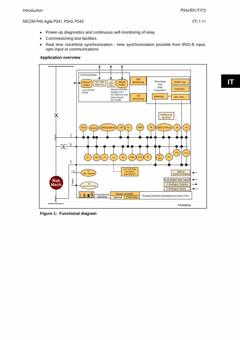
P24x/EN IT/I72 MiCOM P40 Agile P241, P242, P243 (IT) 1-11
IT
• Power-up diagnostics and continuous self-monitoring of relay • Commissioning test facilities • Real time clock/time synchronization - time synchronization possible from IRIG-B input,
opto input or communications
Application overview
Event Log.
Conventional signaling
Always availableRotating Machine Management Relay P24x
4 Analogue Inputs
4 Analogue Outputs
8-16 Digital Opto Inputs
P243 Only
IRIG-BSynchronization
Rot.Mach.
Fault Rec.
Metering
RecordingAndData
Acquisition
SelfMonitoring
CBMonitoring
Communication
Local (RS232)Setting
Fiber OpticRear Port
Ambient airBy RTD
37 32R 47 27 59 59N 81U 55 27 Abs
50/51 50N/51N 50N/51N/67N 32N 40 50BF 66
87
4648/51LR/51S 49
(Up to 10 RTD)26
(Rot. Speed)14
>>>>
I
V
Optional
I
P4069ENc
X
REARPORT
FRONT PORT
2nd
PortRear
Event Log.
Dist. Rec.
Remote (RS485)Modbus RTUIEC 60870-5-103Kbus-CourierIEC 61850
CTSVTS
Low Volt Ride Through &
Auto-Restart
Figure 1: Functional diagram
P24x/EN IT/I72
Introduction (IT)1-12 MiCOM P40 Agile P241, P242, P243
IT
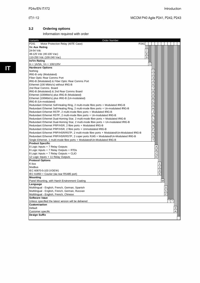
3.2 Ordering options Information required with order
VariantsP241 Motor Protection Relay (40TE Case) P241Vx Aux Rating24-54 Vdc 748-125 Vdc (40-100 Vac) 8110-250 Vdc (100-240 Vac) 9In/Vn RatingIn = 1A/5A, Vn = 100/120V 1Hardware OptionsNothing 1IRIG-B only (Modulated) 2Fiber Optic Rear Comms Port 3IRIG-B (Modulated) & Fiber Optic Rear Comms Port 4Ethernet (100 Mbits/s) without IRIG-B 62nd Rear Comms. Board 7IRIG-B (Modulated) & 2nd Rear Comms Board 8Ethernet (100Mbit/s) plus IRIG-B (Modulated) AEthernet (100Mbit/s) plus IRIG-B (Un-modulated) BIRIG-B (Un-modulated) CRedundant Ethernet Self-Healing Ring, 2 multi-mode fibre ports + Modulated IRIG-B GRedundant Ethernet Self-Healing Ring, 2 multi-mode fibre ports + Un-modulated IRIG-B HRedundant Ethernet RSTP, 2 multi-mode fibre ports + Modulated IRIG-B JRedundant Ethernet RSTP, 2 multi-mode fibre ports + Un-modulated IRIG-B KRedundant Ethernet Dual-Homing Star, 2 multi-mode fibre ports + Modulated IRIG-B LRedundant Ethernet Dual-Homing Star, 2 multi-mode fibre ports + Un-modulated IRIG-B MRedundant Ethernet PRP/HSR, 2 fibre ports + Modulated IRIG-B NRedundant Ethernet PRP/HSR, 2 fibre ports + Unmodulated IRIG-B PRedundant Ethernet PRP/HSR/RSTP, 2 multi-mode fibre ports + Modulated/Un-Modulated IRIG-B RRedundant Ethernet PRP/HSR/RSTP, 2 coper ports RJ45 + Modulated/Un-Modulated IRIG-B SSingle Ethernet, 1 multi-mode fibre ports + Modulated/Un-Modulated IRIG-B TProduct Specific8 Logic Inputs + 7 Relay Outputs A8 Logic Inputs + 7 Relay Outputs + RTDs B8 Logic Inputs + 7 Relay Outputs + CLIO C12 Logic Inputs + 11 Relay Outputs EProtocol OptionsK-bus 1Modbus 2IEC 60870-5-103 (VDEW) 3IEC 61850 + Courier (via rear RS485 port) 6MountingPanel Mounting, with Harsh Environment Coating MLanguageMultilingual - English, French, German, Spanish 0Multilingual - English, French, German, Russian 5Multilingual - English, French, Chinese CSoftware IssueUnless specified the latest version will be delivered * *CustomisationDefault 0Customer specific ADesign Suffix
Order Number
Introduction
P24x/EN IT/I72 MiCOM P40 Agile P241, P242, P243 (IT) 1-13
IT
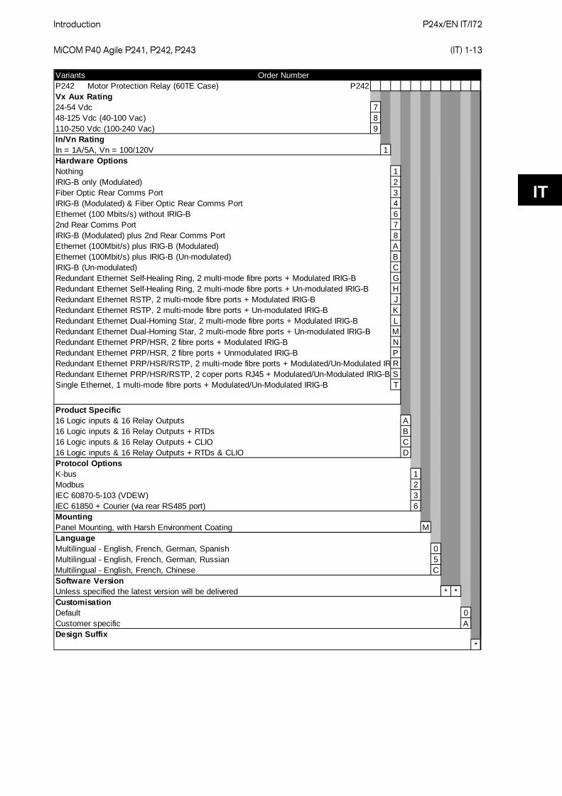
VariantsP242 Motor Protection Relay (60TE Case) P242Vx Aux Rating24-54 Vdc 748-125 Vdc (40-100 Vac) 8110-250 Vdc (100-240 Vac) 9In/Vn RatingIn = 1A/5A, Vn = 100/120V 1Hardware OptionsNothing 1IRIG-B only (Modulated) 2Fiber Optic Rear Comms Port 3IRIG-B (Modulated) & Fiber Optic Rear Comms Port 4Ethernet (100 Mbits/s) without IRIG-B 62nd Rear Comms Port 7IRIG-B (Modulated) plus 2nd Rear Comms Port 8Ethernet (100Mbit/s) plus IRIG-B (Modulated) AEthernet (100Mbit/s) plus IRIG-B (Un-modulated) BIRIG-B (Un-modulated) CRedundant Ethernet Self-Healing Ring, 2 multi-mode fibre ports + Modulated IRIG-B GRedundant Ethernet Self-Healing Ring, 2 multi-mode fibre ports + Un-modulated IRIG-B HRedundant Ethernet RSTP, 2 multi-mode fibre ports + Modulated IRIG-B JRedundant Ethernet RSTP, 2 multi-mode fibre ports + Un-modulated IRIG-B KRedundant Ethernet Dual-Homing Star, 2 multi-mode fibre ports + Modulated IRIG-B LRedundant Ethernet Dual-Homing Star, 2 multi-mode fibre ports + Un-modulated IRIG-B MRedundant Ethernet PRP/HSR, 2 fibre ports + Modulated IRIG-B NRedundant Ethernet PRP/HSR, 2 fibre ports + Unmodulated IRIG-B PRedundant Ethernet PRP/HSR/RSTP, 2 multi-mode fibre ports + Modulated/Un-Modulated IR RRedundant Ethernet PRP/HSR/RSTP, 2 coper ports RJ45 + Modulated/Un-Modulated IRIG-B SSingle Ethernet, 1 multi-mode fibre ports + Modulated/Un-Modulated IRIG-B T
Product Specific16 Logic inputs & 16 Relay Outputs A16 Logic inputs & 16 Relay Outputs + RTDs B16 Logic inputs & 16 Relay Outputs + CLIO C16 Logic inputs & 16 Relay Outputs + RTDs & CLIO DProtocol OptionsK-bus 1Modbus 2IEC 60870-5-103 (VDEW) 3IEC 61850 + Courier (via rear RS485 port) 6MountingPanel Mounting, with Harsh Environment Coating MLanguageMultilingual - English, French, German, Spanish 0Multilingual - English, French, German, Russian 5Multilingual - English, French, Chinese CSoftware VersionUnless specified the latest version will be delivered * *CustomisationDefault 0Customer specific ADesign Suffix
*
Order Number

P24x/EN IT/I72
Introduction (IT)1-14 MiCOM P40 Agile P241, P242, P243
IT
VariantsP243 Motor Protection Relay (80TE Case) P243Vx Aux Rating24-54 Vdc 748-125 Vdc (40-100 Vac) 8110-250 Vdc (100-240 Vac) 9In/Vn RatingIn = 1A/5A, Vn = 100/120V 1Hardware OptionsNothing 1IRIG-B only (Modulated) 2Fiber Optic Rear Comms Port 3IRIG-B (Modulated) & Fiber Optic Rear Comms Port 4Ethernet (100 Mbits/s) without IRIG-B 62nd Rear Comms Port 7IRIG-B (Modulated) & 2nd Rear Comms Port 8Ethernet (100Mbit/s) plus IRIG-B (Modulated) AEthernet (100Mbit/s) plus IRIG-B (Un-modulated) BIRIG-B (Un-modulated) CRedundant Ethernet Self-Healing Ring, 2 multi-mode fibre ports + Modulated IRIG-B GRedundant Ethernet Self-Healing Ring, 2 multi-mode fibre ports + Un-modulated IRIG-B HRedundant Ethernet RSTP, 2 multi-mode fibre ports + Modulated IRIG-B JRedundant Ethernet RSTP, 2 multi-mode fibre ports + Un-modulated IRIG-B KRedundant Ethernet Dual-Homing Star, 2 multi-mode fibre ports + Modulated IRIG-B LRedundant Ethernet Dual-Homing Star, 2 multi-mode fibre ports + Un-modulated IRIG-B MRedundant Ethernet PRP/HSR, 2 fibre ports + Modulated IRIG-B NRedundant Ethernet PRP/HSR, 2 fibre ports + Unmodulated IRIG-B PRedundant Ethernet PRP/HSR/RSTP, 2 multi-mode fibre ports + Modulated/Un-Modulated IRIG-BRRedundant Ethernet PRP/HSR/RSTP, 2 coper ports RJ45 + Modulated/Un-Modulated IRIG-B SSingle Ethernet, 1 multi-mode fibre ports + Modulated/Un-Modulated IRIG-B T
Product Specific16 Logic inputs & 16 Relay Outputs A16 Logic inputs & 16 Relay Outputs + RTDs B16 Logic inputs & 16 Relay Outputs + CLIO C16 Logic inputs & 16 Relay Outputs + RTDs & CLIO DProtocol OptionsK-bus 1Modbus 2IEC 60870-5-103 (VDEW) 3IEC 61850 + Courier (via rear RS485 port) 6MountingPanel Mounting, with Harsh Environment Coating MRack Mounting, with Harsh Environment Coating NLanguageMultilingual - English, French, German, Spanish 0Multilingual - English, French, German, Russian 5Multilingual - English, French, Chinese CSoftware VersionUnless specified the latest version will be delivered * *CustomisationDefault 0Customer specific ADesign Suffix
*
Order Number

Technical Data
P24x/EN TD/I72 MiCOM P40 Agile P241, P242, P243 (TD) 2-1
TD
TECHNICAL DATA

P24x/EN TD/I72
Technical Data (TD) 2-2 MiCOM P40 Agile P241, P242, P243
TD
Technical Data
P24x/EN TD/I72 MiCOM P40 Agile P241, P242, P243 (TD) 2-3
TD
Technical data Mechanical specifications
Design Modular MiCOM Px40 platform relay, P241 in 40TE case, P242 in 60TE case, P243 in 80TE case. Mounting is front of panel flush mounting or 19“ rack mounted (ordering options).
Enclosure protection Per IEC 60529: 1992: IP 52 Protection (front panel) against dust and dripping water, IP 50 Protection for rear and sides of the case, against dust, IP 10 Protection Product safety protection for the rear due to live connections on the terminal block.
Weight P241 (40TE): 7.3kg P242 (60TE): 9.2kg (with RTD, CLIO cards) P243 (80TE): 11.5kg (with RTD, CLIO cards) Terminals
AC current and voltage measuring inputs Located on heavy duty (black) terminal block: Threaded M4 terminals, for ring lug connection. CT inputs have integral safety shorting, upon removal of the terminal block.
General input/output terminals For power supply, opto inputs, output contacts and RP1 rear communications. Located on general purpose (grey) blocks: Threaded M4 terminals, for ring lug connection.
Case protective earth connection Two rear stud connections, threaded M4. Must be earthed (grounded) for safety, minimum earth wire size 2.5 mm2.
Front port serial PC interface EIA(RS)232 DCE, 9 pin D-type female connector Socket SK1. Courier protocol for interface to MiCOM S1 Studio or MiCOM S1 Agile software. Isolation to ELV (extra low voltage) level. Maximum cable length 15 m.
Front download/monitor port EIA(RS)232, 25 pin D-type female connector Socket SK2. For firmware and menu text downloads. Isolation to ELV level.
Rear communications port (RP1) EIA(RS)485 signal levels, two wire connections located on general purpose block, M4 screw. For screened twisted pair cable, multidrop, 1000 m max. For K-Bus, IEC-60870-5-103 or MODBUS Isolation to SELV (safety extra low voltage) level.
Optional rear fiber connection for SCADA/DCS BFOC 2.5 -(ST®)-interface for glass fiber, as per IEC 874-10. 850 nm short-haul fibers, one Tx and one Rx. For Courier, IEC-60870-5-103 or MODBUS
Optional second rear communications port (RP2) EIA(RS)232, 9 pin D-type female connector, socket SK4. Courier protocol: K-Bus, EIA(RS)232, or EIA(RS)485 connection. Isolation to SELV level. Optional rear IRIG-B interface modulated or un-modulated BNC plug Isolation to SELV level. 50 ohm coaxial cable. Optional rear Ethernet connection for IEC 61850
10BaseT/100BaseTX communications Interface in accordance with IEEE802.3 and IEC 61850 Isolation: 1.5 kV Connector type: RJ45 Cable type: Screened Twisted Pair (STP)
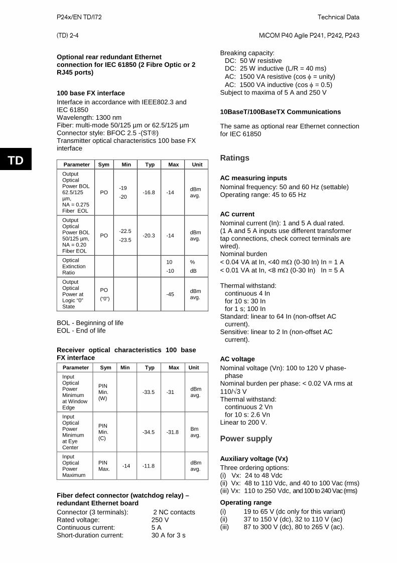
100 base FX interface Interface in accordance with IEEE802.3 and IEC 61850 Wavelength: 1300 nm Fiber: multi-mode 50/125 µm or 62.5/125 µm Connector style: BFOC 2.5 -(ST®)
P24x/EN TD/I72
Technical Data (TD) 2-4 MiCOM P40 Agile P241, P242, P243
TD
Optional rear redundant Ethernet connection for IEC 61850 (2 Fibre Optic or 2 RJ45 ports)
100 base FX interface Interface in accordance with IEEE802.3 and IEC 61850 Wavelength: 1300 nm Fiber: multi-mode 50/125 µm or 62.5/125 µm Connector style: BFOC 2.5 -(ST®) Transmitter optical characteristics 100 base FX interface
Parameter Sym Min Typ Max Unit Output Optical Power BOL 62.5/125 µm, NA = 0.275 Fiber EOL
PO -19 -20
-16.8 -14 dBm avg.
Output Optical Power BOL 50/125 µm, NA = 0.20 Fiber EOL
PO -22.5 -23.5
-20.3 -14 dBm avg.
Optical Extinction Ratio
10 -10
% dB
Output Optical Power at Logic “0” State
PO (“0”)
-45 dBm avg.
BOL - Beginning of life EOL - End of life
Receiver optical characteristics 100 base FX interface
Parameter Sym Min Typ Max Unit Input Optical Power Minimum at Window Edge
PIN Min. (W)
-33.5 -31 dBm avg.
Input Optical Power Minimum at Eye Center
PIN Min. (C)
-34.5 -31.8 Bm avg.
Input Optical Power Maximum
PIN Max. -14 -11.8 dBm
avg.
Fiber defect connector (watchdog relay) – redundant Ethernet board Connector (3 terminals): 2 NC contacts Rated voltage: 250 V Continuous current: 5 A Short-duration current: 30 A for 3 s
Breaking capacity: DC: 50 W resistive DC: 25 W inductive (L/R = 40 ms) AC: 1500 VA resistive (cos φ = unity) AC: 1500 VA inductive (cos φ = 0.5) Subject to maxima of 5 A and 250 V
10BaseT/100BaseTX Communications
The same as optional rear Ethernet connection for IEC 61850 Ratings
AC measuring inputs Nominal frequency: 50 and 60 Hz (settable) Operating range: 45 to 65 Hz
AC current Nominal current (In): 1 and 5 A dual rated. (1 A and 5 A inputs use different transformer tap connections, check correct terminals are wired). Nominal burden < 0.04 VA at In, <40 mΩ (0-30 In) In = 1 A < 0.01 VA at In, <8 mΩ (0-30 In) In = 5 A Thermal withstand: continuous 4 In for 10 s: 30 In for 1 s; 100 In Standard: linear to 64 In (non-offset AC current). Sensitive: linear to 2 In (non-offset AC current).
AC voltage Nominal voltage (Vn): 100 to 120 V phase- phase Nominal burden per phase: < 0.02 VA rms at 110/√3 V Thermal withstand: continuous 2 Vn for 10 s: 2.6 Vn Linear to 200 V. Power supply
Auxiliary voltage (Vx) Three ordering options: (i) Vx: 24 to 48 Vdc (ii) Vx: 48 to 110 Vdc, and 40 to 100 Vac (rms) (iii) Vx: 110 to 250 Vdc, and 100 to 240 Vac (rms)
Operating range (i) 19 to 65 V (dc only for this variant) (ii) 37 to 150 V (dc), 32 to 110 V (ac) (iii) 87 to 300 V (dc), 80 to 265 V (ac).
Technical Data
P24x/EN TD/I72 MiCOM P40 Agile P241, P242, P243 (TD) 2-5
TD
With a tolerable ac ripple of up to 12% for a dc supply, per IEC 60255-11: 1979.
Nominal burden Quiescent burden: 11 W. (Extra 1.25 W when fitted with second rear communications board). Additions for energized binary inputs/outputs: Per opto input: 0.09 W (24 to 54 V), 0.12 W (110/125 V), 0.19 W (220/250 V). Per energized output relay: 0.13 W
Power-up time Time to power up < 11 s.
Power supply interruption 3 power supply options: (i) Vx: 24 to 48 V dc (ii) Vx: 48 to 110 V dc, 40 to 100 V ac (rms) (iii) (i) Vx: 110 to 250 V dc, 100 to 240 V ac (rms) Per IEC 60255-11: 2008 The relay will withstand a 100% interruption in the DC supply without de-energizing as follows: (i) Vx: 24 to 48 V dc Quescent / half load 20 ms at 24 V 50 ms at 36 V 100 ms at 48 V maximum loading: 20 ms at 24 V 50 ms at 36V 100 ms at 48 V (ii) Vx: 48 to 110 V dc Quescent / half load 20 ms at 36 V 50 ms at 60 V 100 ms at 72 V 200 ms at 110 V maximum loading: 20 ms at 36 V 50 ms at 60 V 100 ms at 85 V 200 ms at 110 V (iii) (i) Vx: 110 to 250 V dc Quescent / half load 50 ms at 110 V 100 ms at 160 V 200 ms at 210 V maximum loading: 20 ms at 85 V 50 ms at 98V 100 ms at 135 V 200 ms at 174 V Per IEC 60255-11: 2008: The relay will withstand an interruption in the AC supply without de-energizing as follows: (ii) Vx = 40 to 100 V ac Quescent / half load 50 ms at 27 V for 100% voltage dip
maximum loading: 10 ms at 27 V for 100% voltage dip (iii) Vx = 100 to 240 V ac Quescent / half load 50 ms at 80 V for 100% voltage dip maximum loading: 50 ms at 80 V for 100% voltage dip Maximum loading = all digital inputs/outputs energized Quescent or 1/2 loading = 1/2 of all digital inputs/outputs energized
Battery backup Front panel mounted Type ½ AA, 3.6 V Lithium Thionyl Chloride Battery (SAFT advanced battery reference LS14250) Battery life (assuming relay energized for 90% time) >10 years
Field voltage output Regulated 48 Vdc Current limited at 112 mA maximum output Operating range 40 to 60 V with alarm at <35 V.
Digital (“Opto”) inputs Universal opto inputs with programmable voltage thresholds (24/27, 30/34, 48/54, 110/125, 220/250 V). May be energized from the 48 V field voltage, or the external battery supply. Rated nominal voltage: 24 to 250 Vdc Operating range: 19 to 265 Vdc Withstand: 300 Vdc, 300 Vrms. Peak current of opto input when energized is 3.5 mA (0-300 V) Nominal pick-up and reset thresholds: Nominal battery 24/27: 60 - 80% DO/PU (logic 0) <16.2 (logic 1) >19.2 Nominal battery 24/27: 50 - 70% DO/PU (logic 0) <12.0 (logic 1) >16.8 Nominal battery 30/34: 60 - 80% DO/PU (logic 0) <20.4 (logic 1) >24.0 Nominal battery 30/34: 50 - 70% DO/PU (logic 0) <15.0 (logic 1) >21.0 Nominal battery 48/54: 60 - 80% DO/PU (logic 0) <32.4 (logic 1) >38.4 Nominal battery 48/54: 50 - 70% DO/PU (logic 0) <24.0 (logic 1) >33.6 Nominal battery 110/125: 60 - 80% DO/PU (logic 0) <75.0 (logic 1) >88.0 Nominal battery 110/125: 50 - 70% DO/PU (logic 0) <55.0 (logic 1) >77.0 Nominal battery 220/250: 60 - 80% DO/PU (logic 0) <150.0 (logic 1) >176.0 Nominal battery 220/250: 50 - 70% DO/PU (logic 0) <110 (logic 1) >154 Recognition time: <2 ms with long filter removed, <12 ms with half cycle ac immunity filter on
P24x/EN TD/I72
Technical Data (TD) 2-6 MiCOM P40 Agile P241, P242, P243
TD
Output contacts
Standard contacts General purpose relay outputs for signaling, tripping and alarming: Continuous Carry Ratings (Not Switched): Maximum continuous current: 10 A (UL: 8 A) Short duration withstand carry: 30 A for 3 s 250 A for 30 ms Rated voltage: 300 V Make & Break Capacity: DC: 50 W resistive DC: 62.5 W inductive (L/R = 50 ms) AC: 2500 VA resistive (cos φ = unity) AC: 2500 VA inductive (cos φ = 0.7) Make, Carry: 30 A for 3 secs, dc resistive, 10,000 operations (subject to the above limits of make / break capacity and rated voltage) Make, Carry & Break: 30 A for 200 ms, ac resistive, 2,000 operations (subject to the above limits of make / break capacity & rated voltage) 4 A for 1.5 secs, dc resistive, 10,000 operations (subject to the above limits of make / break capacity & rated voltage) 0.5 A for 1 sec, dc inductive, 10,000 operations (subject to the above limits of make / break capacity & rated voltage) 10 A for 1.5 secs, ac resistive / inductive, 10,000 operations (subject to the above limits of make / break capacity & rated voltage) Durability: Loaded contact: 10 000 operations minimum, Unloaded contact: 100 000 operations minimum. Operate Time Less than 5 ms Reset Time Less than 5 ms
Watchdog contacts Non-programmable contacts for relay healthy/relay fail indication: Breaking capacity: DC: 30 W resistive DC: 15 W inductive (L/R = 40 ms) AC: 375 VA inductive (cos φ = 0.7)
IRIG-B 12X Interface (modulated) External clock synchronization per IRIG standard 200-98, format B12x Input impedance 6 kΩ at 1000 Hz
Modulation ratio: 3:1 to 6:1 Input signal, peak-peak: 200 mV to 20 V
IRIG-B 00X Interface (Un-modulated) External clock synchronization per IRIG standard 200-98, format B00X. Input signal TTL level Input impedance at dc 10 kΩ
Environmental conditions
Ambient temperature range Per IEC 60255-6: 1988: Operating temperature range: -25°C to +55°C (or -13°F to +131°F) Storage and transit: -25°C to +70°C (or -13°F to +158°F) Per IEC 60068-2-1: 2007 -25°C storage (96 hours) -40°C operation (96 hours) Per IEC 60068-2-2: 2007 +85°C storage (96 hours) +85°C operation (96 hours)
Ambient humidity range Per IEC 60068-2-3: 1969: 56 days at 93% relative humidity and +40 °C Per IEC 60068-2-30: 1980 Damp heat cyclic, six (12 + 12) hour cycles, 93% RH, +25 to +55°C
Corrosive environments Per IEC 60068-2-60: 1995, Part 2, Test Ke, Method (class) 3 Industrial corrosive environment/poor environmental control, mixed gas flow test. 21 days at 75% relative humidity and +30oC exposure to elevated concentrations of H2S, NO2, Cl2 and SO2. Type tests
Insulation Per IEC 60255-27: 2005: Insulation resistance > 100 MΩ at 500 Vdc (Using only electronic/brushless insulation tester).
Creepage distances and clearances IEC 60255-27: 2005 Pollution degree 3, Overvoltage category III, Impulse test voltage 5 kV.
High voltage (dielectric) withstand (i) Per IEC 60255-27: 2005, 2 kV rms
Technical Data
P24x/EN TD/I72 MiCOM P40 Agile P241, P242, P243 (TD) 2-7
TD
AC, 1 minute: Between all independent circuits. Between independent circuits and protective (earth) conductor terminal. 1 kV rms AC for 1 minute, across open watchdog contacts. 1 kV rms AC for 1 minute, across open contacts of changeover output relays. 1 kV rms AC for 1 minute for all D-type EIA(RS)232/EIA(RS)485 ports between the communications port terminals and protective (earth) conductor terminal. (ii) Per ANSI/IEEE C37.90-1989 (reaffirmed 1994): 1.5 kV rms AC for 1 minute, across open contacts of normally open output relays. 1 kV rms AC for 1 minute, across open watchdog contacts. 1 kV rms AC for 1 minute, across open contacts of changeover output relays.
Impulse voltage withstand test Per IEC 60255-27: 2005: Front time: 1.2 µs, Time to half-value: 50 µs, Peak value: 5 kV, 0.5J Between all independent circuits. Between all independent circuits and protective (earth) conductor terminal. Between the terminals of independent circuits. EIA(RS)232 & EIA(RS)485 ports and normally open contacts of output relays excepted. Electromagnetic compatibility (EMC) 1 MHz burst high frequency disturbance test Per IEC 60255-22-1: 1988, Class III, Common-mode test voltage: 2.5 kV, Differential test voltage: 1.0 kV, Test duration: 2 s, Source impedance: 200 Ω (EIA(RS)232 ports excepted). Damped oscillatory test Per EN61000-4-18: 2007 + A1: 2010: Level 3 100 kHz and 1 MHz Common mode test voltage: 2.5 kV Power Supply, Relay contacts, CT, VT, Opto Input, Communications, IRIG-B Differential mode test voltage: 1 kV Power Supply, Relay contacts, CT, VT, Opto Input 3 MHz, 10 MHz and 30 MHz Common mode test voltage: 4 kV Power Supply, Relay contacts, CT, VT, Opto Input, Communications, IRIG-B
Immunity to electrostatic discharge Per IEC 60255-22-2: 1996, Class 4, 15 kV discharge in air to user interface, display, communication port and exposed metalwork. 8 kV point contact discharge to any part of the front of the product.
Electrical fast transient or burst requirements Per IEC 60255-22-4: 2002 and EN61000-4-4:2004. Test severity Class III and IV: Amplitude: 2 kV, burst frequency 5 kHz (Class III), Amplitude: 4 kV, burst frequency 2.5 kHz (Class IV). Applied directly to auxiliary supply, and applied to all other inputs. (EIA(RS)232 ports excepted). Amplitude: 4 kV, burst frequency 5 kHz (Class IV) applied directly to auxiliary.
Surge withstand capability Per IEEE/ANSI C37.90.1: 2002: 4 kV fast transient and 2.5 kV oscillatory
applied directly across each output contact, optically isolated input, and power supply circuit.
4 kV fast transient and 2.5 kV oscillatory applied common mode to communications, IRIG-B.
Surge immunity test (EIA(RS)232 ports excepted). Per IEC 61000-4-5: 2005 Level 4, Time to half-value: 1.2 / 50 µs, Amplitude: 4 kV between all groups and protective (earth) conductor terminal,
Amplitude: 2 kV between terminals of each group.
Conducted/radiated immunity For RTDs used for tripping applications the conducted and radiated immunity performance is guaranteed only when using totally shielded RTD cables (twisted leads).
Immunity to radiated electromagnetic energy Per IEC 60255-22-3: 2000, Class III: Test field strength, frequency band 80 to 1000 MHz: 10 V/m, Test using AM: 1 kHz / 80%, Spot tests at 80, 160, 450, 900 MHz Per IEEE/ANSI C37.90.2: 2004: 80 MHz to 1000 MHz, 1 kHz 80% am and am pulsed modulated. Field strength of 35 V/m.
Radiated immunity from digital communications Per EN61000-4-3: 2002, Level 4: Test field strength, frequency band 800 to 960 MHz, and 1.4 to 2.0 GHz: 30 V/m, Test using AM: 1 kHz/80%.
P24x/EN TD/I72
Technical Data (TD) 2-8 MiCOM P40 Agile P241, P242, P243
TD
Radiated immunity from digital radio telephones Per IEC 61000-4-3: 2002: 10 V/m, 900 MHz and 1.89 GHz.
Immunity to conducted disturbances induced by radio frequency fields Per IEC 61000-4-6: 1996, Level 3, Disturbing test voltage: 10 V.
Power frequency magnetic field immunity Per IEC 61000-4-8: 1994, Level 5, 100 A/m applied continuously, 1000 A/m applied for 3s. Per IEC 61000-4-9: 1993, Level 5, 1000 A/m applied in all planes. Per IEC 61000-4-10: 1993, Level 5, 100 A/m applied in all planes at 100 kHz/1 MHz with a burst duration of 2 s.
Conducted emissions Per EN 55022: 1998 Class A: 0.15 - 0.5 MHz, 79 dBµV (quasi peak) 66 dBµV (average) 0.5 – 30 MHz, 73 dBµV (quasi peak) 60 dBµV (average).
Radiated emissions Per EN 55022: 1998 Class A: 30 – 230 MHz, 40 dBµV/m at 10 m measurement distance 230 – 1 GHz, 47 dBµV/m at 10 m measurement distance. EU directives
EMC compliance Per 2006/95/EC: Compliance to the European Commission Directive on EMC is claimed via the Technical Construction File route. Product Specific Standards were used to establish conformity: EN50263: 2000
Product safety Compliance to the European Commission Low Voltage Directive. (LVD) is demonstrated using a Technical File. A product specific standard was used to establish conformity. EN 60255-27: 2005
R&TTE compliance Radio and Telecommunications Terminal Equipment (R & TTE) directive 99/5/EC. Compliance demonstrated by compliance to both the EMC directive and Low voltage directive, down to zero volts. Applicable to rear communications ports.
ATEX compliance ATEX Potentially Explosive Atmospheres directive 94/9/EC, for equipment. The equipment is compliant with Article 1(2) of European directive 94/9/EC. It is approved for operation outside an ATEX hazardous area. It is however approved for connection to Increased Safety, “Ex e”, motors with rated ATEX protection, Equipment Category 2, to ensure their safe operation in gas Zones 1 and 2 hazardous areas. CAUTION - Equipment with this marking is not itself suitable for operation within a potentially explosive atmosphere. Compliance demonstrated by Notified Body certificates of compliance.
II (2) G
Note: Programmable IDMT curves shall not be used for ATEX applications. ATEX marked models are only approved for use with a fixed IDMT curve. Mechanical robustness
Vibration test Per IEC 60255-21-1: 1996: Response Class 2 Endurance Class 2
Shock and bump Per IEC 60255-21-2: 1996: Shock response Class 2 Shock withstand Class 1 Bump Class 1
Seismic test Per IEC 60255-21-3: 1995: Class 2
Transit Packaging Performance Product testing to simulate protection offered by primary packaging carton, to ISTA 1C specification
Vibration and Drop Release Tests:
Technical Data
P24x/EN TD/I72 MiCOM P40 Agile P241, P242, P243 (TD) 2-9
TD
Vibration tests in 3 orientations, vibratory
movement 7 Hz, amplitude 5.3 mm, acceleration 1.05g Drop tests - 10 drops from 61 cm height on multiple carton faces, edges and corners
P24x third party compliances Underwriters laboratory (UL)
File Number: E202519 Original Issue Date: 21-04-2005 (Complies with Canadian and US requirements). Energy Networks Association (ENA)
Certificate Number: 104 Issue 2 Assessment Date: 16-04-2004
P24x/EN TD/I72
Technical Data (TD) 2-10 MiCOM P40 Agile P241, P242, P243
TD
Protection functions Thermal overload
Accuracy Setting accuracy: ±5% Reset: 97% of thermal setting ±5% Thermal alarm Pick-up: Calculated trip time ±5% or 40 ms whichever is greater Thermal overload Pick-up: Calculated trip time ±5% or 40 ms whichever is greater Cooling time accuracy: ±5% of theoretical Repeatability: <2.5% 4-Stage non-directional short-circuit protection
Accuracy Pick-up: Setting ±5% Drop-off: 0.95 x Setting ±5% Minimum trip level (IDMT): 1.05 x Setting ±5% IDMT characteristic shape: ±5% or 40 ms whichever is greater* IEEE reset: ±5% or 50 ms whichever is greater DT operation: ±2% or 50 ms whichever is greater DT Reset: ±5% Characteristic UK: IEC 6025-3…1998 Characteristic US: IEEE C37.112…1996 * Under reference conditions Sensitive directional earth fault
SEF Accuracy Pick-up: Setting ±5% Drop-off: 0.95 x Setting ±5% IDMT trip level elements: 1.05 x Setting ±5% IDMT characteristic shape: ±5% or 40 ms whichever is greater IEEE reset: ±5% or 40 ms whichever is greater DT operation: ±2% or 40 ms whichever is greater DT reset: ±5% Repeatability: <2.5%
Wattmetric SEF accuracy P = 0W Pick-up: PO> ±5% P > 0W Pick-up: P> ±5% P = 0W Drop-off: (0.95 x ISEF>) ±5% P > 0W Drop-off: 0.9 x P> ±5% Boundary accuracy: ±5% with 1° hysteresis Repeatability: <2.5%
Polarizing quantities accuracy Operating boundary Pick-up: ±2° of RCA ±90° Hysteresis: <3° ISEF>Vnpol Pick-up: Setting ±10% ISEF>Vnpol Drop-off: 0.9 x Setting or 0.7 V (whichever is greater) ±10% 2-Stage negative phase sequence overcurrent
Accuracy I2>Pick-up: Setting ±5% I2> Drop-off: 0.95 x Setting ±5% Vpol Pick-up: Setting ±5% Vpol Drop-off: 0.95 x Setting ±5% DT operation: ±2% or 40 ms whichever is greater IDMT operation: ±5% or 40 ms whichever is greater 3 Phase voltage check
Accuracy Pick-up: Setting ±5% Drop-off: 0.95 x Setting ±5% Repeatability (operating threshold): <1% Repeatability (operating times): <10 ms 2-Stage directional/non-directional derived earth fault
Accuracy Pick-up: Setting ±5% Drop-off: 0.95 x Setting ±5% IDMT trip level elements: 1.05 x Setting ±5% IDMT characteristic shape: ±5% or 40 ms whichever is greater IEEE reset: ±5% or 40 ms whichever is greater DT operation: ±2% or 40 ms whichever is greater DT reset: ±5% Repeatability: 2.5% Zero polarizing Operating pick-up: ±2%o of RCA ±90% Hysteresis: <3° VN > Pick-up: Setting ±10% VN > Drop-off: 0.9 x Setting ±10% Negative polarizing Operating Pick-up: ±2%o of RCA ±90% Hysteresis: <3° VN 2 > Pick-up: Setting ±10% VN 2 > Drop-off: 0.9 x Setting ±10% I2 > Pick up: Setting ±10% I2 > Drop-off: 0.9 x Setting ±10%
Technical Data
P24x/EN TD/I72 MiCOM P40 Agile P241, P242, P243 (TD) 2-11
TD
Stall protection Pick-up: Setting ±5%
Timer accuracy Timers: ±2% or 40 ms whichever is greater Reset time: <30 ms Motor differential protection
Accuracy Pick-up: Formula ±5% Drop-off: 95% of setting ±5% Operating time: <30 ms for currents applied at 4x pickup level or greater Repeatability: <7.5% Disengagement time: <40 ms Neutral displacement/residual overvoltage
Accuracy DT/IDMT Pick-up: Setting ±5% Drop-off: 0.95 x Setting ±5% IDMT characteristic shape: ±5% or 40 ms whichever is greater DT operation: ±2% 40 ms whichever is greater Instantaneous operation <55 ms Reset: <35 ms Repeatability: <1% Loss of load
Accuracy Pick-up: Setting ±5% or 2 W Drop-off: 0.95 of setting ±5% Angle variation Pick-up: Expected pick-up angle ±2 degree Angle variation Drop-off: Expected drop-off angle ±2.5 degree Operating time: ±2% or 40 ms whichever is greater Repeatability: <5% Disengagement time: <50 ms tRESET: ±5% Instantaneous operating time: <50 ms Out of step Pick-up: Setting ±5% DT operation: ±2% or 40 ms whichever is greater
Reverse power
Accuracy Pick-up: Setting ±5% or 2 W Drop-off: 0.95 of setting ±5% Angle variation Pick-up: Expected pick-up angle ±2 degree Angle variation Drop-off: Expected drop-off angle ±2.5 degree Operating time: ±2% or 40 ms whichever is greater Repeatability: <5% Disengagement time: <50 ms tRESET: ±5% Instantaneous operating time: <50 ms Anti-backspin Pick-up: Setting ±5% DT operation: ±2% or 40 ms whichever is greater Repeatability: <1% Field failure
Accuracy Mho characteristic Pick-up: Characteristic shape ±5% Linear characteristic Pick-up: Characteristic shape ±10% Mho characteristic Drop-off: 105% of setting ±5% Linear characteristic Drop-off: 105% of setting ±10% Operating time: ±2% or 60 ms whichever is greater Repeatability: <1% Disengagement time: <50 ms Voltage protection Undervoltage
Accuracy DT Pick-up: Setting ±5% IDMT Pick-up: (0.95 x Setting) ±5% Drop-off: 1.05 x Setting ±5% IDMT characteristic shape: ±5% or 40 ms whichever is greater DT operation: ±2% or 40 ms whichever is greater Reset: <75 ms Repeatability: <1%
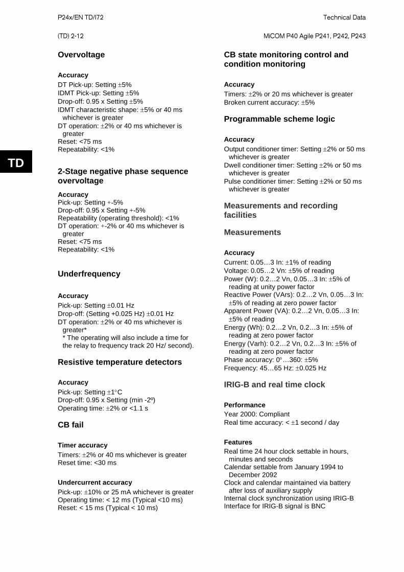
P24x/EN TD/I72
Technical Data (TD) 2-12 MiCOM P40 Agile P241, P242, P243
TD
Overvoltage
Accuracy DT Pick-up: Setting ±5% IDMT Pick-up: Setting ±5% Drop-off: 0.95 x Setting ±5% IDMT characteristic shape: ±5% or 40 ms whichever is greater DT operation: ±2% or 40 ms whichever is greater Reset: <75 ms Repeatability: <1%
2-Stage negative phase sequence overvoltage Accuracy Pick-up: Setting +-5% Drop-off: 0.95 x Setting +-5% Repeatability (operating threshold): <1% DT operation: +-2% or 40 ms whichever is greater Reset: <75 ms Repeatability: <1% Underfrequency Accuracy Pick-up: Setting ±0.01 Hz Drop-off: (Setting +0.025 Hz) ±0.01 Hz DT operation: ±2% or 40 ms whichever is greater* * The operating will also include a time for the relay to frequency track 20 Hz/ second). Resistive temperature detectors
Accuracy Pick-up: Setting ±1°C Drop-off: 0.95 x Setting (min -2º) Operating time: ±2% or <1.1 s CB fail
Timer accuracy Timers: ±2% or 40 ms whichever is greater Reset time: <30 ms
Undercurrent accuracy Pick-up: ±10% or 25 mA whichever is greater Operating time: < 12 ms (Typical <10 ms) Reset: < 15 ms (Typical < 10 ms)
CB state monitoring control and condition monitoring
Accuracy Timers: ±2% or 20 ms whichever is greater Broken current accuracy: ±5% Programmable scheme logic
Accuracy Output conditioner timer: Setting ±2% or 50 ms whichever is greater Dwell conditioner timer: Setting ±2% or 50 ms whichever is greater Pulse conditioner timer: Setting ±2% or 50 ms whichever is greater Measurements and recording facilities Measurements
Accuracy Current: 0.05…3 In: ±1% of reading Voltage: 0.05…2 Vn: ±5% of reading Power (W): 0.2…2 Vn, 0.05…3 In: ±5% of reading at unity power factor Reactive Power (VArs): 0.2…2 Vn, 0.05…3 In: ±5% of reading at zero power factor Apparent Power (VA): 0.2…2 Vn, 0.05…3 In: ±5% of reading Energy (Wh): 0.2…2 Vn, 0.2…3 In: ±5% of reading at zero power factor Energy (Varh): 0.2…2 Vn, 0.2…3 In: ±5% of reading at zero power factor Phase accuracy: 0°…360: ±5% Frequency: 45…65 Hz: ±0.025 Hz IRIG-B and real time clock
Performance Year 2000: Compliant Real time accuracy: < ±1 second / day
Features Real time 24 hour clock settable in hours, minutes and seconds Calendar settable from January 1994 to December 2092 Clock and calendar maintained via battery after loss of auxiliary supply Internal clock synchronization using IRIG-B Interface for IRIG-B signal is BNC
Technical Data
P24x/EN TD/I72 MiCOM P40 Agile P241, P242, P243 (TD) 2-13
TD
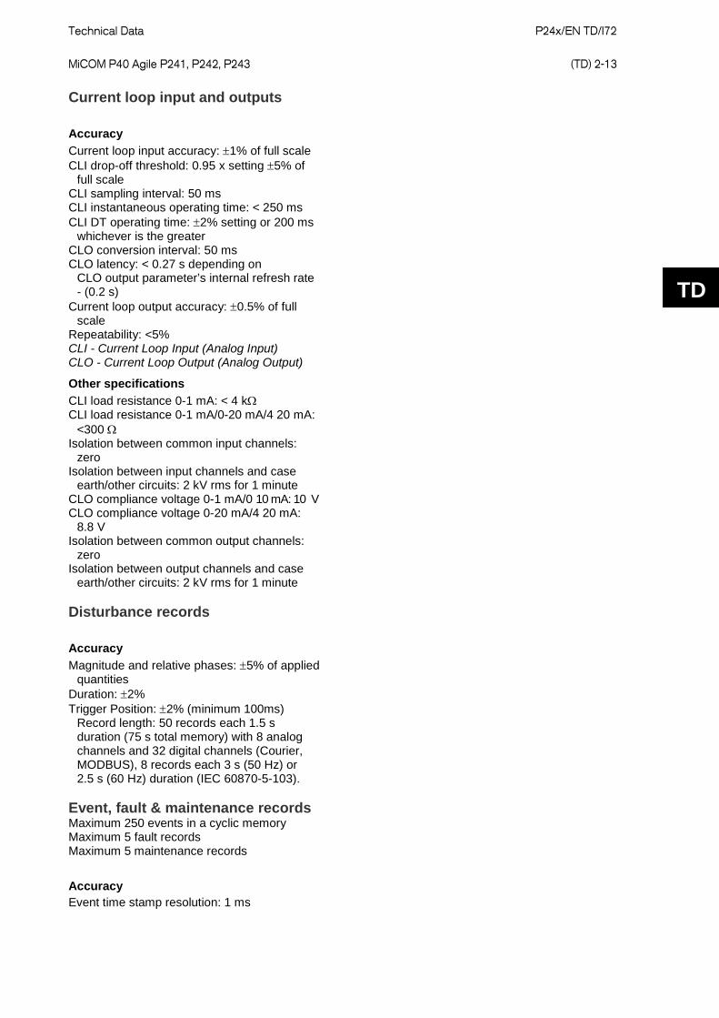
Current loop input and outputs
Accuracy Current loop input accuracy: ±1% of full scale CLI drop-off threshold: 0.95 x setting ±5% of full scale CLI sampling interval: 50 ms CLI instantaneous operating time: < 250 ms CLI DT operating time: ±2% setting or 200 ms whichever is the greater CLO conversion interval: 50 ms CLO latency: < 0.27 s depending on CLO output parameter’s internal refresh rate - (0.2 s) Current loop output accuracy: ±0.5% of full scale Repeatability: <5% CLI - Current Loop Input (Analog Input) CLO - Current Loop Output (Analog Output)
Other specifications CLI load resistance 0-1 mA: < 4 kΩ CLI load resistance 0-1 mA/0-20 mA/4 20 mA: <300 Ω Isolation between common input channels: zero Isolation between input channels and case earth/other circuits: 2 kV rms for 1 minute CLO compliance voltage 0-1 mA/0 10 mA: 10 V CLO compliance voltage 0-20 mA/4 20 mA: 8.8 V Isolation between common output channels: zero Isolation between output channels and case earth/other circuits: 2 kV rms for 1 minute Disturbance records
Accuracy Magnitude and relative phases: ±5% of applied quantities Duration: ±2% Trigger Position: ±2% (minimum 100ms)
Record length: 50 records each 1.5 s duration (75 s total memory) with 8 analog channels and 32 digital channels (Courier, MODBUS), 8 records each 3 s (50 Hz) or 2.5 s (60 Hz) duration (IEC 60870-5-103).
Event, fault & maintenance records Maximum 250 events in a cyclic memory Maximum 5 fault records Maximum 5 maintenance records
Accuracy Event time stamp resolution: 1 ms
P24x/EN TD/I72
Technical Data (TD) 2-14 MiCOM P40 Agile P241, P242, P243
TD
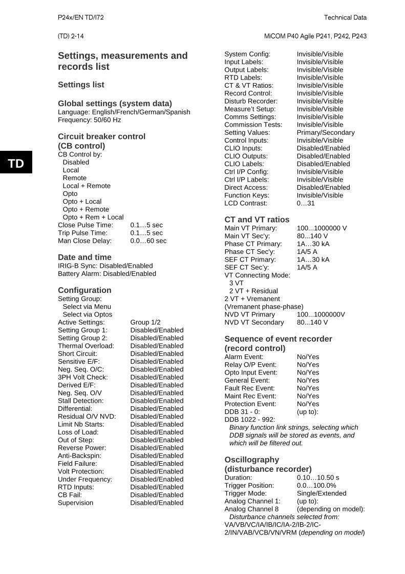
Settings, measurements and records list Settings list Global settings (system data) Language: English/French/German/Spanish Frequency: 50/60 Hz Circuit breaker control (CB control) CB Control by: Disabled Local Remote Local + Remote Opto Opto + Local Opto + Remote Opto + Rem + Local Close Pulse Time: 0.1…5 sec Trip Pulse Time: 0.1…5 sec Man Close Delay: 0.0…60 sec Date and time IRIG-B Sync: Disabled/Enabled Battery Alarm: Disabled/Enabled Configuration Setting Group: Select via Menu Select via Optos Active Settings: Group 1/2 Setting Group 1: Disabled/Enabled Setting Group 2: Disabled/Enabled Thermal Overload: Disabled/Enabled Short Circuit: Disabled/Enabled Sensitive E/F: Disabled/Enabled Neg. Seq. O/C: Disabled/Enabled 3PH Volt Check: Disabled/Enabled Derived E/F: Disabled/Enabled Neg. Seq. O/V Disabled/Enabled Stall Detection: Disabled/Enabled Differential: Disabled/Enabled Residual O/V NVD: Disabled/Enabled Limit Nb Starts: Disabled/Enabled Loss of Load: Disabled/Enabled Out of Step: Disabled/Enabled Reverse Power: Disabled/Enabled Anti-Backspin: Disabled/Enabled Field Failure: Disabled/Enabled Volt Protection: Disabled/Enabled Under Frequency: Disabled/Enabled RTD Inputs: Disabled/Enabled CB Fail: Disabled/Enabled Supervision Disabled/Enabled
System Config: Invisible/Visible Input Labels: Invisible/Visible Output Labels: Invisible/Visible RTD Labels: Invisible/Visible CT & VT Ratios: Invisible/Visible Record Control: Invisible/Visible Disturb Recorder: Invisible/Visible Measure’t Setup: Invisible/Visible Comms Settings: Invisible/Visible Commission Tests: Invisible/Visible Setting Values: Primary/Secondary Control Inputs: Invisible/Visible CLIO Inputs: Disabled/Enabled CLIO Outputs: Disabled/Enabled CLIO Labels: Disabled/Enabled Ctrl I/P Config: Invisible/Visible Ctrl I/P Labels: Invisible/Visible Direct Access: Disabled/Enabled Function Keys: Invisible/Visible LCD Contrast: 0…31 CT and VT ratios Main VT Primary: 100...1000000 V Main VT Sec'y: 80...140 V Phase CT Primary: 1A…30 kA Phase CT Sec'y: 1A/5 A SEF CT Primary: 1A…30 kA SEF CT Sec’y: 1A/5 A VT Connecting Mode: 3 VT 2 VT + Residual 2 VT + Vremanent (Vremanent phase-phase) NVD VT Primary 100...1000000V NVD VT Secondary 80...140 V Sequence of event recorder (record control) Alarm Event: No/Yes Relay O/P Event: No/Yes Opto Input Event: No/Yes General Event: No/Yes Fault Rec Event: No/Yes Maint Rec Event: No/Yes Protection Event: No/Yes DDB 31 - 0: (up to): DDB 1022 - 992: Binary function link strings, selecting which DDB signals will be stored as events, and which will be filtered out. Oscillography (disturbance recorder) Duration: 0.10…10.50 s Trigger Position: 0.0…100.0% Trigger Mode: Single/Extended Analog Channel 1: (up to): Analog Channel 8 (depending on model): Disturbance channels selected from: VA/VB/VC/IA/IB/IC/IA-2/IB-2/IC-2/IN/VAB/VCB/VN/VRM (depending on model)
Technical Data
P24x/EN TD/I72 MiCOM P40 Agile P241, P242, P243 (TD) 2-15
TD
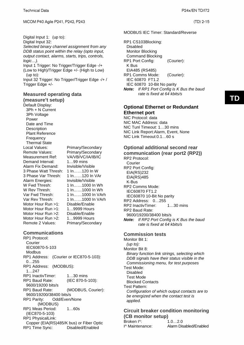
Digital Input 1: (up to): Digital Input 32: Selected binary channel assignment from any DDB status point within the relay (opto input, output contact, alarms, starts, trips, controls, logic…). Input 1 Trigger: No Trigger/Trigger Edge -/+ (Low to High)/Trigger Edge +/- (High to Low) (up to): Input 32 Trigger: No Trigger/Trigger Edge -/+ / Trigger Edge +/- Measured operating data (measure’t setup) Default Display: 3Ph + N Current 3Ph Voltage Power Date and Time Description Plant Reference Frequency Thermal State Local Values: Primary/Secondary Remote Values: Primary/Secondary Measurement Ref: VA/VB/VC/IA/IB/IC Demand Interval: 1…99 mins Alarm Fix Demand: Invisible/Visible 3 Phase Watt Thresh: 1 In……120 In W 3 Phase Var Thresh: 1 In……120 In VAr Alarm Energies: Invisible/Visible W Fwd Thresh: 1 In……1000 In Wh W Rev Thresh: 1 In……1000 In Wh Var Fwd Thresh: 1 In……1000 In VArh Var Rev Thresh: 1 In……1000 In VArh Motor Hour Run >1: Disable/Enable Motor Hour Run >1: 1…9999 Hours Motor Hour Run >2: Disable/Enable Motor Hour Run >2: 1…9999 Hours Remote 2 Values: Primary/Secondary Communications RP1 Protocol: Courier IEC60870-5-103 Modbus RP1 Address: (Courier or IEC870-5-103): 0…255 RP1 Address: (MODBUS): 1…247 RP1 InactivTimer: 1…30 mins RP1 Baud Rate: (IEC 870-5-103): 9600/19200 bits/s RP1 Baud Rate: (MODBUS, Courier): 9600/19200/38400 bits/s RP1 Parity: Odd/Even/None (MODBUS) RP1 Meas Period: 1…60s (IEC870-5-103) RP1 PhysicalLink: Copper (EIA(RS)485/K bus) or Fiber Optic RP1 Time Sync: Disabled/Enabled
MODBUS IEC Timer: Standard/Reverse RP1 CS103Blocking: Disabled Monitor Blocking Command Blocking RP1 Port Config: (Courier): K Bus EIA485 (RS485) RP1 Comms Mode: (Courier): IEC 60870 FT1.2 IEC 60870 10-Bit No parity Note: If RP1 Port Config is K Bus the baud rate is fixed at 64 kbits/s
Optional Ethernet or Redundant Ethernet port NIC Protocol: data NIC MAC Address: data NIC Tunl Timeout: 1…30 mins NIC Link Report:Alarm, Event, None NIC Link Timeout:0.1…60 s Optional additional second rear communication (rear port2 (RP2)) RP2 Protocol: Courier RP2 Port Config: EIA(RS)232 EIA(RS)485 K-Bus RP2 Comms Mode: IEC60870 FT1.2 IEC60870 10-Bit No parity RP2 Address: 0…255 RP2 InactivTimer: 1…30 mins RP2 Baud Rate: 9600/19200/38400 bits/s Note: If RP2 Port Config is K Bus the baud rate is fixed at 64 kbits/s Commission tests Monitor Bit 1: (up to): Monitor Bit 8: Binary function link strings, selecting which DDB signals have their status visible in the Commissioning menu, for test purposes Test Mode: Disabled Test Mode Blocked Contacts Test Pattern: Configuration of which output contacts are to be energized when the contact test is applied. Circuit breaker condition monitoring (CB monitor setup) Broken I^: 1.0…2.0 I^ Maintenance: Alarm Disabled/Enabled
P24x/EN TD/I72
Technical Data (TD) 2-16 MiCOM P40 Agile P241, P242, P243
TD
I^ Maintenance: 1…25000 No. CB Ops Maint: Alarm Disabled/Enabled No. CB Ops Maint: 1…10000 CB Time Maint: Alarm Disabled/Enabled CB Time Maint: 0.005…0.500 s Opto coupled binary inputs (opto config) Global Nominal V: 24 - 27 V 30 - 34 V 48 - 54 V 110 - 125 V 220 - 250 V Custom Opto Input 1: (up to): Opto Input #. (# = max. opto no. fitted): Custom options allow independent thresholds to be set per opto, from the same range as above. Opto Filter Control: Binary function link string, selecting which optos will have an extra 1/2 cycle noise filter, and which will not. Characteristics: Standard 60% - 80% 50% - 70% Time stamping accuracy: ±1 msec Control inputs into PSL (ctrl. I/P config.) Hotkey Enabled: Binary function link string, selecting which of the control inputs will be driven from Hotkeys. Control Input 1: Latched/Pulsed (up to): Control Input 32: Latched/Pulsed Ctrl Command 1: (up to): Ctrl Command 32: ON/OFF SET/RESET IN/OUT ENABLED/DISABLED Function keys Fn. Key Status 1: (up to): Fn. Key Status 10 Disable Lock Unlock/Enable Fn. Key 1 Mode: Toggled/Normal (up to): Fn. Key 10 Mode: Toggled/Normal Fn. Key 1 Label: (up to): Fn. Key 10 Label: User defined text string to describe the function of the particular function key
IED configurator Switch Conf.Bank: No Action/Switch Banks IEC 61850 GOOSE GoEna: Disabled/Enabled Test Mode: Disabled/Pass Through/Forced VOP Test Pattern: 0x00000000... 0xFFFFFFFF Ignore Test Flag: No/Yes Control input user labels (ctrl. I/P labels) Control Input 1:
(up to): Control Input 32: User defined text string to describe the function of the particular control input Settings in multiple groups Note: All settings here onwards apply for setting groups # = 1 to 2.

Technical Data
P24x/EN TD/I72 MiCOM P40 Agile P241, P242, P243 (TD) 2-17
TD
Protection functions System config. Phase Sequence: Standard ABC/Reverse ACB Thermal Ith Current Set: 0.2 In…1.5 In K Coefficient: 0…10 Thermal Const T1: 1min…180min Thermal Const T2: 1min…360min Thermal Const Tr: 1min…999min Thermal Trip: Disabled/Enabled Thermal Alarm: Disabled/Enabled Alarm Threshold: 0.2%…100% Thermal Lockout: Disabled/Enabled Lockout Thresh: 0.2…100% Inh Trip Dur St: Disabled/Enabled Maximum user curve time delay setting 1 x e30 4-stage non-directional short circuit protection Phase O/C: Sub Heading I>1 Function: Disabled DT IEC S Inverse IEC V Inverse IEC E Inverse UK LT Inverse UK Rectifier RI IEEE M Inverse IEEE V Inverse IEEE E Inverse US Inverse US ST Inverse I>1 Current Set: 0.2…15 In I>1 Time Delay: 0.040…100.00 s I>1 TMS: 0.025…1.200 I>1 Time Dial: 0.01…100.00 I>1 K (RI): 0.10…10.00 I>1 Reset Char: DT/Inverse I>1 tRESET: 0.00…100.00 s I>2 as I>1 I>3 Status: Disabled/Enabled I>3 Current Set: 0.20…15.00 In I>3 Time Delay: 0.040…100.00 s I>4 as I>3 Maximum user curve time delay setting 1 x e308
IDMT curves Inverse time (IDMT) characteristic IDMT characteristics are selectable from a choice of four IEC/UK and five IEEE/US curves as shown in the table below.
The IEC/UK IDMT curves conform to the following formula:
t = T x
K
(Ι/Ιs) α - 1 + L
The IEEE/US IDMT curves conform to the following formula:
/ 7/ 1a
Kt TD x LI Is
= + −
Where: t = Operation time K = Constant Ι = Measured current ΙS = Current threshold setting α = Constant L = ANSI/IEEE constant (zero for IEC/UK curves) T = Time multiplier setting for IEC/UK curves TD = Time dial setting for IEEE/US curves IDMT characteristics
IDMT curve Stand. K α L
Standard inverse IEC 0.14 0.02 0
Very inverse IEC 13.5 1 0
Extremely inverse IEC 80 2 0
Long time inverse UK 120 1 0
Moderately inverse IEEE 0.0515 0.02 0.114
Very inverse IEEE 19.61 2 0.491
Extremely inverse IEEE 28.2 2 0.1217
Inverse US-C08 5.95 2 0.18
Short time inverse US-C02 0.16758 0.02 0.11858
The IEC extremely inverse curve becomes definite time at currents greater than 20 x setting. The IEC standard, very and long time inverse curves become definite time at currents greater than 30 x setting. The rectifier curve becomes definite time at currents greater than 8xsttings. The definite time part of the IEC inverse time characteristics at currents greater than 20x and 30x setting are only relevant for currents in the operating range of the relay. The operating range of the P241/2/3 current inputs

P24x/EN TD/I72
Technical Data (TD) 2-18 MiCOM P40 Agile P241, P242, P243
TD
is 0 – 64 In for the standard current inputs and is 0 – 2 In for the sensitive current input. The RI curve (electromechanical) has been included in the first and second stage characteristic setting options for Phase Overcurrent and Earth Fault protections. The curve is represented by the following equation:
t = K x
1
0.339 - ( )0.236/M in seconds
With K adjustable from 0.1 to 10 in steps of 0.05 M = Ι/Ιs For all IEC/UK curves, the reset characteristic is definite time only. For all IEEE/US curves, the reset characteristic can be selected as either inverse curve or definite time. The inverse reset characteristics are dependent upon the selected IEEE/US IDMT curve as shown in the table below. All inverse reset curves conform to the following formula:
tRESET = TD x S
(1 - M2) in seconds
Where: TD = Time dial setting for IEEE curves S = Constant M = Ι/Ιs
Curve description Standard S Moderately inverse IEEE 4.85 Very inverse IEEE 21.6 Extremely inverse IEEE 29.1 Inverse US 5.95 Short time inverse US 2.261
Technical Data
P24x/EN TD/I72 MiCOM P40 Agile P241, P242, P243 (TD) 2-19
TD
Earth fault ISEF>1 Function: Disabled DT IEC S Inverse IEC V Inverse IEC E Inverse UK LT Inverse UK Rectifier IEEE M Inverse IEEE V Inverse IEEE E Inverse US Inverse US ST Inverse ISEF>1 Direction: Non-Directional Directional Fwd ISEF>1 Current: 0.005 In…1 In ISEF>1 T Delay: 0.04…200.0 s ISEF>1 TMS: 0.025…1.2 ISEF>1 Time Dial: 0.5…15 ISEF>1 Reset Chr: DT/Inverse ISEF>1 tReset: 0…100 s ISEF>2 Function: Disabled/Enabled ISEF>2 Direction: Non-Directional Directional Fwd ISEF>2 Current Set: 0.005In…1In ISEF>2 T Delay: 0.04…200 s ISEF> Char Angle: -180°…+180° ISEF> VN Pol Set: 0.5…25 V (Earth Fault Wattmetric) PO> Function: Disabled/Enabled PO> Current Set: 0.005 In…1 In PO> Voltage Set: 0.5…80 V PO> Coeff K Set: 1…10 PO> Char Angle: -180°…+180° PO> Time Delay: 0.04…100 s Negative sequence overcurrent Ι2>1 Status: Disabled/DT Ι2>1 Current Set: 0.05…4 Ιn Ι2>1 Time Delay: 0.04…200 s Ι2>2 Status: Disabled/IMDT Ι2>2 Current Set: 0.05…4 Ιn Ι2>2 TMS: 0.07…2 3 phase voltage check Start Low V Set: 0.1 Vn…1.0 Vn Earth fault derived IN>1 Function: Disabled DT IEC S Inverse IEC V Inverse IEC E Inverse UK LT Inverse UK Rectifier IEEE M Inverse IEEE V Inverse
IEEE E Inverse US Inverse US ST Inverse IN>1 Direction: Non-Directional Directional Fwd IN>1 Current Set: 0.08In…32 In IN>1 T Delay: 0.04…100 s IN>1 TMS: 0.025…1.2 IN>1 Time Dial: 0.5…15 IN>1 Reset Chr: DT/Inverse IN>1 tReset: 0…100 s IN>2 Function: Disabled/DT IN>2 Direction: Non-Directional Directional Fwd IN>2 Current: 0.08 In…32 In IN>2 T Delay: 0.04…100 s IN> Char Angle: -180°…+180° IN> Type Pol Type: Zero Sequence Neg Sequence IN> VN Pol Set: 0.5…25 V IN> V2pol Set: 0.5…25 V IN2> I2pol Set: 0.002 In…0.8 In Maximum user curve time delay setting 1 x e308
Stall detection Prolonged Start: Disabled/Enabled Start Criteria: 52 a I 52 a + I Starting Current: 1*In…5*In Prol Start time: 1…200 s Stall Rotor Strt: Disabled/Enabled Stall Detection: Disabled/Enabled Stall Setting: 1*In…5*In Stall Time: 0.1…60 s Reacceleration: Disabled/Enabled Reacc Low Voltage Setting: 50…120 V LV Ride Thru: Disabled/Enabled Reac. High V Setting: 50…120 V Reac. Time: 0.1…60 s Auto Re-Start: Disabled/Enabled Reac. Long Time: 0…60 s Reac. Shed Time: 0…5940 s
P24x/EN TD/I72
Technical Data (TD) 2-20 MiCOM P40 Agile P241, P242, P243
TD
Motor differential protection Diff Function: Disabled Percentage Bias High Impedance Diff Is1: 0.05…0.50 In Diff k1: 0…20% Diff Is2: 1…5.0 In Diff k2: 20…150.00% Residual O/V NVD VN>1 Function: Disabled DT IDMT VN>1 Voltage Set: 0.5….80 V VN>1 Time Delay: 0.04…100 s VN>1 TMS: 0.05…100 VN>2 Status: Disabled/DT VN>2 Voltage Set: 0.5…80 V VN>2 Time Delay: 0.04…100 s Limit Nb starts Hot Start status: Disabled/Enabled Hot start Nb: 1…5 Cold Start Stat: Disabled/Enabled Cold start Nb: 1…5 Supervising Time: 10…120 min T Betw St Status: Disabled/Enabled Time betw start: 1…120 min Inhib Start Ttime: 1…120 min Loss of load P<1 Status: Disabled/DT P<1 Power Set: 1*In …120*In W P<1 Time Delay: 0.04…100s P<2 Status: Disabled/DT P<2 Power Set: 1*In …120*In W P<2 Time Delay: 0.04…100 s P< Drop-off Time 0.05…300 s Out of step (power factor) PF< Status Lead: Disabled/DT Power Fact lead: 0.1…0.9 PF< Lead TD: 0.05…100 s PF< Status Llag: Disabled/DT Power Fact Lag: 0.1…0.9 PF< Lag TD: 0.05…100 s PF< Drop-off time: 0.05…300 s Reverse power Rev P< Power Set: 1*In…120*In W Rev P< Time Delay: 0.04…100 s Rev P< Drop-of Ti: 0.05…300 s Anti-backspin VRem Anti-backs: 1…120 V Anti-backs Delay: 1…7200 s
Field failure FFail Alm Status: Disabled/Enabled FFail Alm Angle: 15°…75° FFail Alm Delay: 0.00…100.0 s FFail 1 Status: Disabled/Enabled FFail 1 -Xa1: 0…40.0/InΩ FFail 1 Xb1: 25…325.0/InΩ FFail 1 Time Delay: 0…100 s FFail 1 DO Timer: 0…100 s FFail 2 as FFail1 Volt protection Undervoltage V<1 Measurment Mode: Phase-Phase/Any Phase V<1 Function: Disabled DT IDMT V<1 Voltage Set: 15…120 V V<1 Time Delay: 0.04… 600 s V<1 TMS: 0.5…100 V<2 Status: Disabled/DT V<2 Voltage Set: 15…120V V<2 Time Delay: 0.04… 600 s Inhib During St: Disabled/DT Overvoltage V>1 Measurment Mode: Phase-Phase/Any Phase V>1 Status: Disabled/DT V>1 Voltage Set: 50…200 V V>1 time Delay: 0.04… 600 s V>2 Status: Disabled/DT V>2 Voltage Set: 50…200 V V>2 Time Delay: 0.04… 600 s NPS Overvoltage V2>1 Status: Enabled/Disabled V2>1 Voltage Set: 1 to 110 V V2>1 Time Delay: 0.04 to 100 s V2>2 Status: Enabled/Disabled V2>2 Voltage Set: 1 to 110 V V2>2 Time Delay: 0.04 to 100 s
Underfrequency F<1 Status: Disabled/DT F<1 Setting: 45…65 Hz F<1 Time Delay: 0.1…100 s F<2 Status: Disabled/DT F<2 Setting: 45…65 Hz F<2 Time Delay: 0.1…100 s RTD protection Select RTD: Bit 0 - Select RTD 1 Bit 1 - Select RTD 2 Bit 2 - Select RTD 3 Bit 3 - Select RTD 4
Technical Data
P24x/EN TD/I72 MiCOM P40 Agile P241, P242, P243 (TD) 2-21
TD
Bit 4 - Select RTD 5 Bit 5 - Select RTD 6 Bit 6 - Select RTD 7 Bit 7 - Select RTD 8 Bit 8 - Select RTD 9 Bit 9 - Select RTD 10 Binary function link string, selecting which RTDs (1 - 10) are enabled. RTD 1 Alarm Set: 0°C…200°C RTD 1 Alarm Dly: 0s…100s RTD 1 Trip Set: 0°C…200°C RTD 1 Trip Dly: 0s…100s RTD2/3/4/5/6/7/8/9/10 as RTD1 Ext. Temp. Influence: Disabled/DT Ext. Temp. RTD: 1…10 Ext. RTD Back-up: 1…10 Type RTD: PT100 Ni100 Ni120 RTD Unit: Degree Celsius Fahrenheit CB fail CB Fail 1 Status: Disabled/Enabled CB Fail 1 Timer: 0.00…10.00 s CB Fail 2 Status: Disabled/Enabled CB Fail 2 Timer: 0.00…10.00 s CBF Non I Reset: I< Only, CB Open & I<, Prot Reset & I< CBF Ext Reset: I< Only, CB Open & I <, Prot Reset & I< I< Current Set: 0.02…3.200 In Supervisory functions Voltage transformer supervision (fuse failure)
Accuracy Fast block operation: <25 ms Fast block reset: <30 ms Time delay: Setting ±2% or 20 ms whichever is greater Current transformer supervision
Accuracy IN > Pick-up: Setting ±5% VN < Pick-up: Setting ±5% IN > Drop-off: 0.9 x Setting ±5% VN < Drop-off: (1.05 x Setting) ±5% or 1 V whichever is greater CTS block operation: < 1 cycle CTS reset: < 35 ms Input labels Opto Input 1…16: Opto 1…Opto 16
User defined text string to describe the function of the particular opto input. Output labels Relay 1…16: Relay 1…Relay 16 User defined text string to describe the function of the particular relay output contact. RTD labels RTD 1-10: RTD1…RTD10 User defined text string to describe the function of the particular RTD. CLIO labels CLIO Input 1…16: Analog Input 1…Analog Input 16 User defined text string to describe the function of the particular analog input. Analogue Input (current loop input) CLIO Inputs Range 1: Disabled 0 - 1 mA 0 - 10 mA 0 - 20 mA 4 - 20 mA Unit 1: Unit Range None -32.5 k...50 k A 0...100 k V 0...20 k Hz 0...100 W -1.41 G...1.41 G Var -1.41 G...1.41 G VA 0...1.41 G °C -40...400 F -40...752 % 0...150 s 0...300 Minimum 1: As above for unit range Maximum 1: As above for unit range Function 1: Disabled/Enabled Alarm Set 1: As above for unit range Alarm Delay 1: 0…300 s Trip Set 1: As above for unit range Trip Delay 1: 0…300 s Drop-off Time: 0.1…300 CLI2/3/4 as CLI1 Analogue output (current loop output) CLIO Outputs Range 1: 0 - 1 mA 0 - 10 mA 0 - 20 mA 4 - 20 mA ANALOG OUTPUT 1: As shown below*
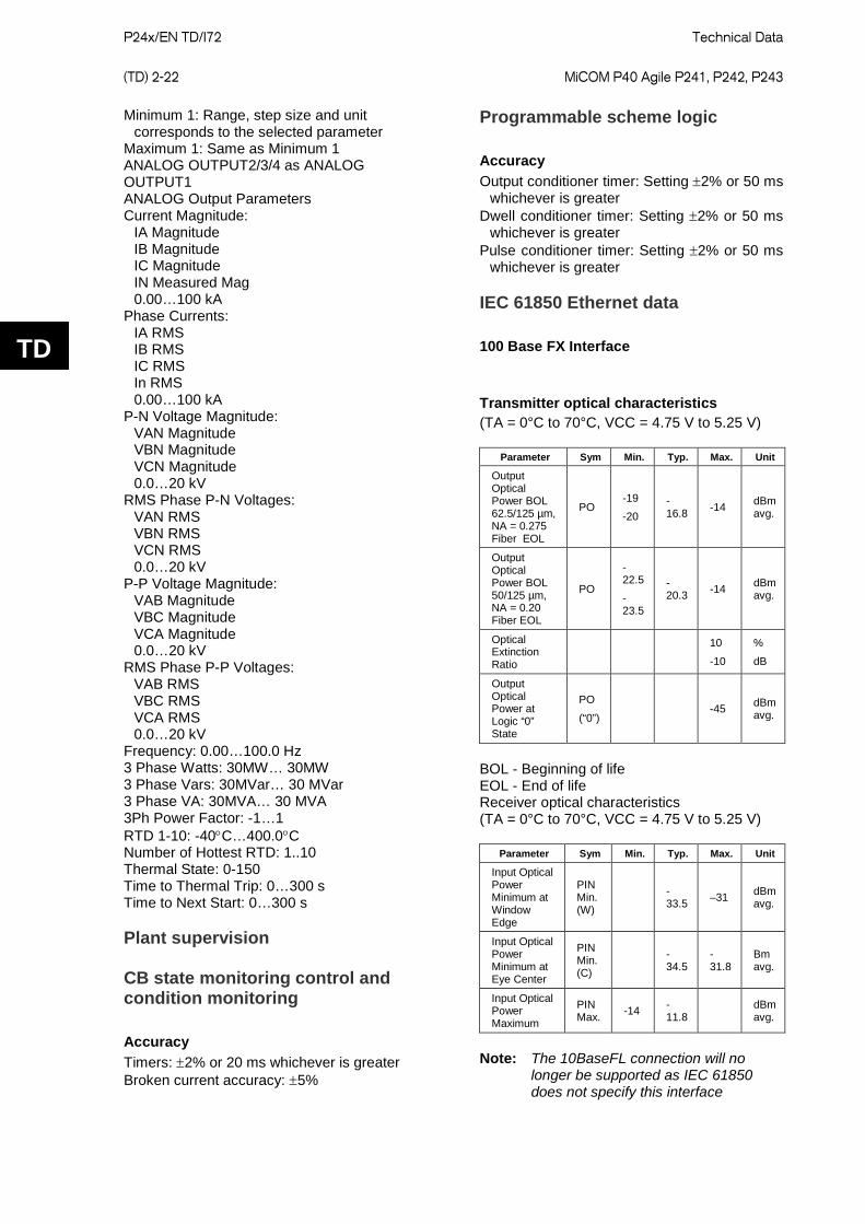
P24x/EN TD/I72
Technical Data (TD) 2-22 MiCOM P40 Agile P241, P242, P243
TD
Minimum 1: Range, step size and unit corresponds to the selected parameter Maximum 1: Same as Minimum 1 ANALOG OUTPUT2/3/4 as ANALOG OUTPUT1 ANALOG Output Parameters Current Magnitude: IA Magnitude IB Magnitude IC Magnitude IN Measured Mag 0.00…100 kA Phase Currents: IA RMS IB RMS IC RMS In RMS 0.00…100 kA P-N Voltage Magnitude: VAN Magnitude VBN Magnitude VCN Magnitude 0.0…20 kV RMS Phase P-N Voltages: VAN RMS VBN RMS VCN RMS 0.0…20 kV P-P Voltage Magnitude: VAB Magnitude VBC Magnitude VCA Magnitude 0.0…20 kV RMS Phase P-P Voltages: VAB RMS VBC RMS VCA RMS 0.0…20 kV Frequency: 0.00…100.0 Hz 3 Phase Watts: 30MW… 30MW 3 Phase Vars: 30MVar… 30 MVar 3 Phase VA: 30MVA… 30 MVA 3Ph Power Factor: -1…1 RTD 1-10: -40°C…400.0°C Number of Hottest RTD: 1..10 Thermal State: 0-150 Time to Thermal Trip: 0…300 s Time to Next Start: 0…300 s Plant supervision CB state monitoring control and condition monitoring
Accuracy Timers: ±2% or 20 ms whichever is greater Broken current accuracy: ±5%
Programmable scheme logic
Accuracy Output conditioner timer: Setting ±2% or 50 ms whichever is greater Dwell conditioner timer: Setting ±2% or 50 ms whichever is greater Pulse conditioner timer: Setting ±2% or 50 ms whichever is greater IEC 61850 Ethernet data
100 Base FX Interface
Transmitter optical characteristics (TA = 0°C to 70°C, VCC = 4.75 V to 5.25 V)
Parameter Sym Min. Typ. Max. Unit
Output Optical Power BOL 62.5/125 µm, NA = 0.275 Fiber EOL
PO -19
-20 -16.8 -14 dBm
avg.
Output Optical Power BOL 50/125 µm, NA = 0.20 Fiber EOL
PO
-22.5
-23.5
-20.3 -14 dBm
avg.
Optical Extinction Ratio
10
-10
%
dB
Output Optical Power at Logic “0” State
PO
(“0”) -45 dBm
avg.
BOL - Beginning of life EOL - End of life Receiver optical characteristics (TA = 0°C to 70°C, VCC = 4.75 V to 5.25 V)
Parameter Sym Min. Typ. Max. Unit
Input Optical Power Minimum at Window Edge
PIN Min. (W)
-33.5 –31 dBm
avg.
Input Optical Power Minimum at Eye Center
PIN Min. (C)
-34.5
-31.8
Bm avg.
Input Optical Power Maximum
PIN Max. -14 -
11.8 dBm avg.
Note: The 10BaseFL connection will no longer be supported as IEC 61850 does not specify this interface
Technical Data
P24x/EN TD/I72 MiCOM P40 Agile P241, P242, P243 (TD) 2-23
TD
Measurements list Measurements 1 Iϕ Magnitude Iϕ Phase Angle Per phase (ϕ = A, B, C) current measurements IN Derived Mag IN Derived Angle ISEF Magnitude ISEF Angle I1 magnitude I2 magnitude I0 Magnitude Iϕ RMS Per phase (ϕ = A, B, C) RMS current measurements Vϕ-ϕ Magnitude Vϕ-ϕ Phase Angle Vϕ Magnitude Vϕ Phase Angle All phase-phase and phase-neutral voltages (ϕ = A, B, C, N). Vr Antibacks Mag V1 Magnitude V2 Magnitude Vϕ RMS Vϕ-ϕ RMS All phase-phase and phase-neutral voltages (ϕ = A, B, C, AB, BC, CA). Frequency Ratio I2/I1 IA2 Magnitude IA2 Angle IB2 Magnitude IB2 Angle IC2 Magnitude IC2 Angle IA Differential IB Differential IC Differential IA Bias IB Bias IC Bias Measurements 2 3 Phase Watts 3 Phase VArs 3 Phase VA Zero Seq Power 3Ph Power Factor 3Ph WHours Fwd 3Ph WHours Rev 3Ph VArHours Fwd 3Ph VArHours Rev Reset Energies: No/Yes 3Ph W Fix Demand 3Ph VArs Fix Dem 3Ph W Peak Dem 3Ph VAr Peak Dem Reset Demand: No/Yes 3Ph I Maximum
3Ph V Maximum Reset Maximum I/V: No/Yes Measurements 3 (model specific) Thermal Load Thermal State Time to Th Trip Reset Th State: No/Yes RTD#1 Temperature…… ……...to RTD#10 Temperature Nb of Hot St Allow Nb of Cold St Allow Time to Next St Emergency Rest: No/Yes Last Start Time Last St Current Nb of Starts Reset Nb of St: No/Yes Nb Emergency Rst Reset Nb Em Rst: No/Yes Nb of Reaccelerat Reset Nb of Reacc: No/Yes Motor Run Time Reset Motor Run T: No/Yes RTD open Cct RTD Short Cct RTD Data Error Reset RTD Flags: No/Yes Nb Hottest RTD Hottest RTD Temp Reset Max RTD Temp: No/Yes Analog Input 1 Analog Input 2 Analog Input 3 Analog Input 4 Measurements 4 (model specific) Nb Control trips Nb Thermal Trip Nb Trip I> 1 Nb Trip I> 2 Nb Trip I> 3 Nb Trip I> 4 Nb Trip V2>1 Nb Trip V2>2 Nb Trip Vdip Nb Trip ISEF>1 Nb Trip ISEF>2 Nb Trip IN>1 Nb Trip IN>2 Nb Trip I2>1 Nb Trip I2> 2 Nb Trip P0> Nb Trip V<1 Nb Trip V<2 Nb Trip F<1 Nb Trip F<2 Nb F.Fail1 Trip Nb F.Fail2 Trip Nb Trip P<1 Nb Trip P<2 Nb Trip PF< Lead
P24x/EN TD/I72
Technical Data (TD) 2-24 MiCOM P40 Agile P241, P242, P243
TD
Nb Trip PF< Lag Nb Trip Rev P Nb Trip V> 1 Nb Trip V> 2 Nb Trip VN>1 Nb Trip VN>2 Nb Prolong St Nb Lock Rot-sta Nb Lock-Rot-run Nb Trip RTD#1…Nb Trip RTD#10 Nb Trip Diff Nb A Input 1Trip Nb A Input 2Trip Nb A Input 3Trip Nb A Input 4Trip Nb FFail1 Trip Nb FFail2 Trip Nb Trip I>3 Nb Trip I>4 Reset Trip Stat: No/Yes CB condition CB Operations Total Iϕ Broken Cumulative breaker interruption duty on a per phase basis (ϕ = A, B, C). CB Operate Time Reset CB Data: No/Yes

Getting Started
P24x/EN GS/I72 MiCOM P40 Agile P241, P242, P243 (GS) 3-1
GS
GETTING STARTED

P24x/EN GS/I72
Getting Started (GS) 3-2 MiCOM P40 Agile P241, P242, P243
GS
Getting Started
P24x/EN GS/I72 MiCOM P40 Agile P241, P242, P243 (GS) 3-3
GS
CONTENTS
1 GETTING STARTED 7
1.1 User interfaces and menu structure 7
1.2 Introduction to the relay 7
1.2.1 Front panel 7
1.2.1.1 LED indications 9
1.2.2 Relay rear panel 10
1.3 Relay connection and power-up 11
1.4 Introduction to the user interfaces and settings options 12
1.5 Menu structure 12
1.5.1 Protection settings 13
1.5.2 Disturbance recorder settings 13
1.5.3 Control and support settings 13
1.6 Password protection 14
1.7 Relay configuration 15
1.8 Front panel user interface (keypad and LCD) 15
1.8.1 Default display and menu time-out 16
1.8.2 Menu navigation and setting browsing 16
1.8.3 Hotkey menu navigation 16
1.8.3.1 Setting group selection 17
1.8.3.2 Control inputs – user assignable functions 17
1.8.3.3 CB control 17
1.8.4 Password entry 17
1.8.5 Reading and clearing of alarm messages and fault records 18
1.8.6 Setting changes 18
1.9 Front communication port user interface 19
1.9.1 Front courier port 20
1.10 MiCOM S1 Studio relay communications basics 21
1.10.1 PC requirements 21
1.10.2 Connecting to the relay using MiCOM S1 Studio 21
1.10.3 Off-line use of MiCOM S1 Studio 22
1.11 The User Programmable Curve Tool (UPCT) 22
1.11.1 Supporting software versions 22
1.11.2 Application advantages of user-programmable curves 22
1.11.3 The main features and overview of the User Configurable Curve Tool: 22
2 CONFIGURING THE ETHERNET INTERFACE 24
2.1 Configuring the Ethernet Interface for IEC 61850 24
2.2 Configuring the Ethernet Interface for DNP3.0 25
3 CONFIGURING THE REDUNDANT ETHERNET BOARD 27
P24x/EN GS/I72
Getting Started (GS) 3-4 MiCOM P40 Agile P241, P242, P243
GS
3.1 Configuring the IED IP address 27
3.2 Configuring the Board IP Address 27
3.3 RSTP Configuration 28
4 CONFIGURING THE DATA PROTOCOLS 34
4.1 Courier Configuration 34
4.2 DNP3.0 configuration 35
4.3 IEC 60870-5-103 Configuration 36
4.4 IEC 61850 Configuration 38
4.5 DNP3.0 Configuration Using MiCOM S1 Agile 38
4.6 IEC 61850 Configuration 38
4.6.1 IEC 61850 Configuration Banks 38
4.6.2 IEC 61850 Network Connectivity 39
5 PRP/HSR CONFIGURATOR 40
5.1 Connecting the IED to a PC 40
5.2 Installing the Configurator 40
5.3 Starting the Configurator 40
5.4 PRP/HSR device identification 41
5.5 Selecting the device mode 41
5.6 PRP/HSR IP Address Configuration 41
5.7 SNTP IP Address Configuration 41
5.8 Check for connected equipment 41
5.9 PRP Configuration 41
5.10 HSR Configuration 42
5.11 Filtering Database 42
5.12 End of session 43
FIGURES Figure 1: Relay front view (P241) 7
Figure 2: Relay front view (P242/3) 8
Figure 3: Relay rear view 11
Figure 4: Menu structure 13
Figure 5: Front panel user interface 15
Figure 6: Hotkey menu navigation 17
Figure 7: Front port connection 19
Figure 8: PC - relay signal connection 20
Figure 9: IED amd REB IP address configuration 27
Figure 10: REB address switches (SW2) 28
Figure 11: Connection using (a) an Ethernet switch and (b) a Media Cover 40

Getting Started
P24x/EN GS/I72 MiCOM P40 Agile P241, P242, P243 (GS) 3-5
GS
TABLES Table 1: P241 default mappings for programmable LEDs 9
Table 2: P242/3 default mappings for programmable LEDs 10
Table 3: Auxiliary voltage options 11
Table 4: Information and controls accessed from available interfaces 12
Table 5: Access levels 14
Table 6: Front port pin designation 19
Table 7: DTE devices serial port pin designation 19
Table 8: Front port fixed communication settings 20

P24x/EN GS/I72
Getting Started (GS) 3-6 MiCOM P40 Agile P241, P242, P243
GS
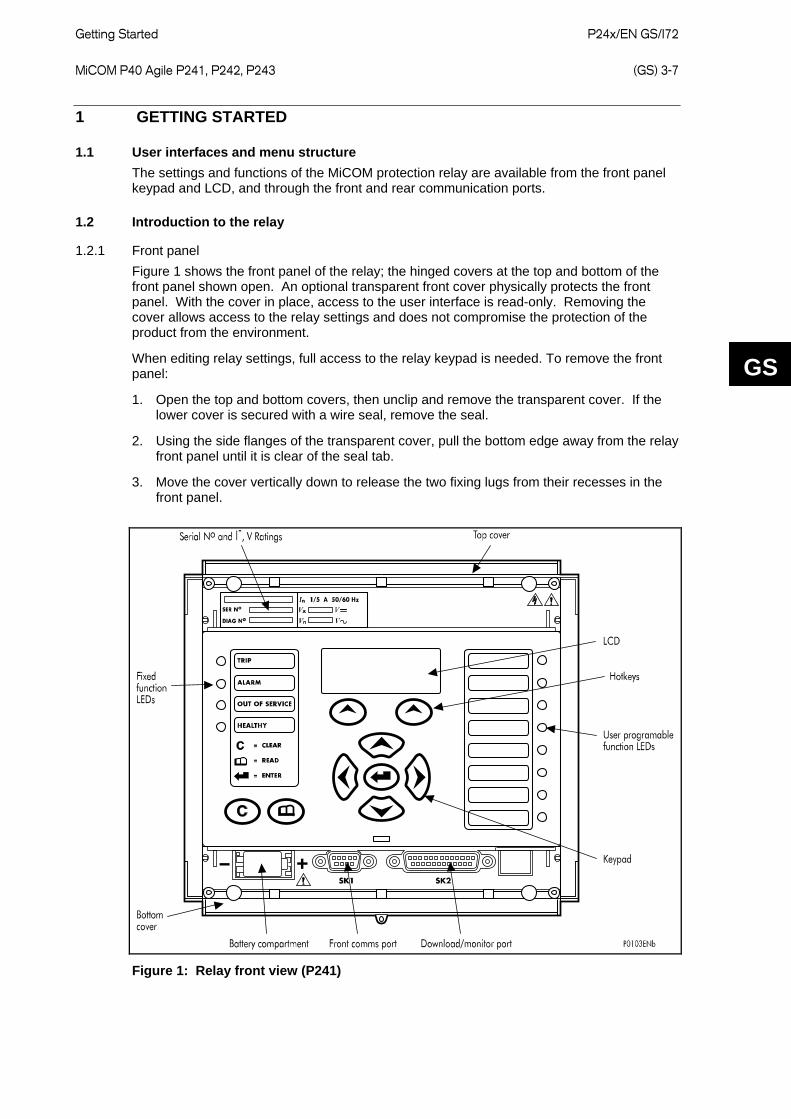
Getting Started
P24x/EN GS/I72 MiCOM P40 Agile P241, P242, P243 (GS) 3-7
GS
1 GETTING STARTED
1.1 User interfaces and menu structure The settings and functions of the MiCOM protection relay are available from the front panel keypad and LCD, and through the front and rear communication ports.
1.2 Introduction to the relay
1.2.1 Front panel Figure 1 shows the front panel of the relay; the hinged covers at the top and bottom of the front panel shown open. An optional transparent front cover physically protects the front panel. With the cover in place, access to the user interface is read-only. Removing the cover allows access to the relay settings and does not compromise the protection of the product from the environment.
When editing relay settings, full access to the relay keypad is needed. To remove the front panel:
1. Open the top and bottom covers, then unclip and remove the transparent cover. If the lower cover is secured with a wire seal, remove the seal.
2. Using the side flanges of the transparent cover, pull the bottom edge away from the relay front panel until it is clear of the seal tab.
3. Move the cover vertically down to release the two fixing lugs from their recesses in the front panel.
Figure 1: Relay front view (P241)
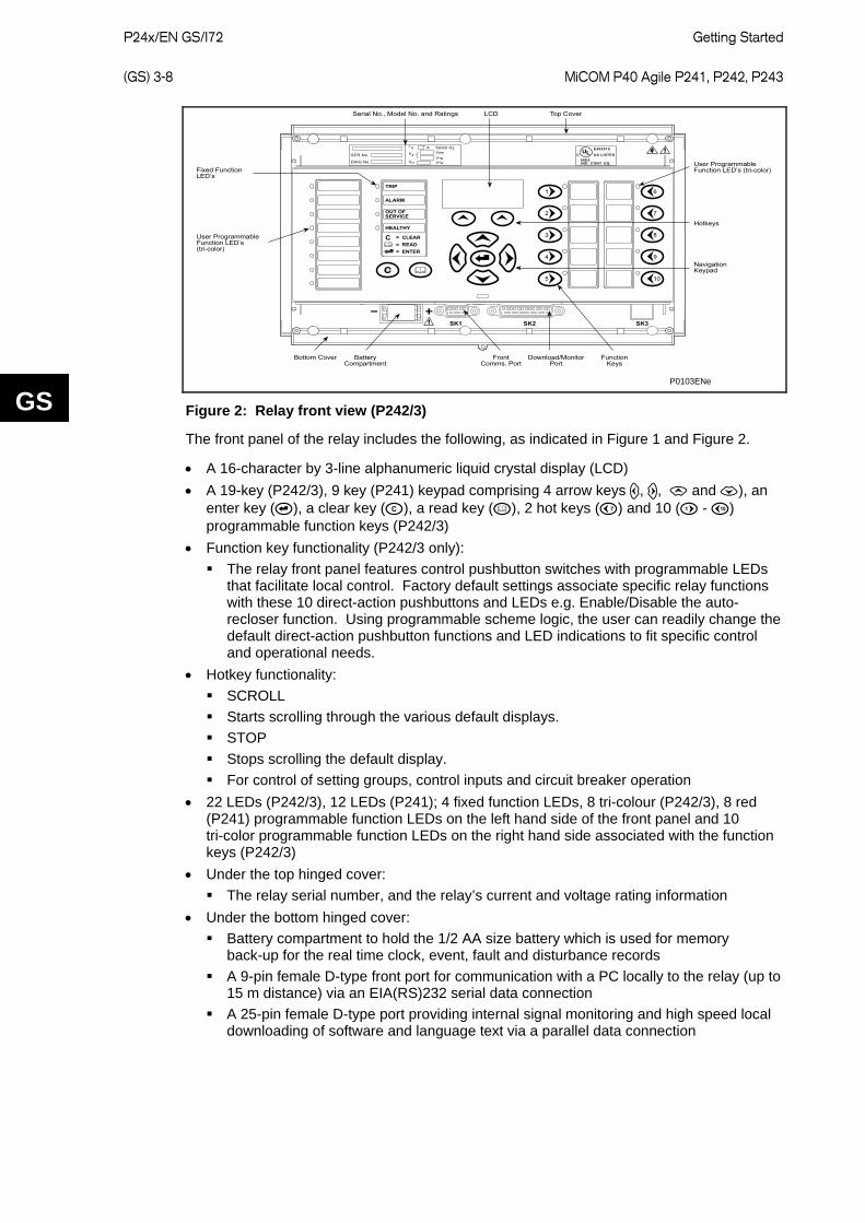
P24x/EN GS/I72
Getting Started (GS) 3-8 MiCOM P40 Agile P241, P242, P243
GS P0103ENe
Figure 2: Relay front view (P242/3)
The front panel of the relay includes the following, as indicated in Figure 1 and Figure 2.
• A 16-character by 3-line alphanumeric liquid crystal display (LCD) • A 19-key (P242/3), 9 key (P241) keypad comprising 4 arrow keys , , and ), an
enter key (), a clear key (), a read key (), 2 hot keys () and 10 ( - ) programmable function keys (P242/3)
• Function key functionality (P242/3 only): The relay front panel features control pushbutton switches with programmable LEDs
that facilitate local control. Factory default settings associate specific relay functions with these 10 direct-action pushbuttons and LEDs e.g. Enable/Disable the auto-recloser function. Using programmable scheme logic, the user can readily change the default direct-action pushbutton functions and LED indications to fit specific control and operational needs.
• Hotkey functionality: SCROLL Starts scrolling through the various default displays. STOP Stops scrolling the default display. For control of setting groups, control inputs and circuit breaker operation
• 22 LEDs (P242/3), 12 LEDs (P241); 4 fixed function LEDs, 8 tri-colour (P242/3), 8 red (P241) programmable function LEDs on the left hand side of the front panel and 10 tri-color programmable function LEDs on the right hand side associated with the function keys (P242/3)
• Under the top hinged cover: The relay serial number, and the relay’s current and voltage rating information
• Under the bottom hinged cover: Battery compartment to hold the 1/2 AA size battery which is used for memory
back-up for the real time clock, event, fault and disturbance records A 9-pin female D-type front port for communication with a PC locally to the relay (up to
15 m distance) via an EIA(RS)232 serial data connection A 25-pin female D-type port providing internal signal monitoring and high speed local
downloading of software and language text via a parallel data connection
Getting Started
P24x/EN GS/I72 MiCOM P40 Agile P241, P242, P243 (GS) 3-9
GS
1.2.1.1 LED indications Fixed Function
The four fixed-function LEDs on the left-hand side of the front panel are used to indicate the following conditions:
• Trip (Red) indicates that the relay has issued a trip signal. It is reset when the associated fault record is cleared from the front display.
• Alarm (Yellow) flashes when the relay registers an alarm. This may be triggered by a fault, event or maintenance record. The LED flashes until the alarms have been accepted (read), then changes to constantly ON. When the alarms are cleared, the LED switches off.
• Out of service (Yellow) is ON when the relay’s protection is unavailable.
• Healthy (Green) is ON when the relay is in correct working order, and should be ON at all times. It goes OFF if the relay’s self-tests show there is an error in the relay’s hardware or software. The state of the healthy LED is reflected by the watchdog contact at the back of the relay.
To adjust the LCD contrast from the CONFIGURATION column, select LCD Contrast. This is only necessary in very hot or cold ambient temperatures.
Programmable LEDs
All the programmable LEDs are tri-color in the P242/3 and can be programmed to indicate RED, YELLOW or GREEN depending on the requirements. All the programmable LEDs are RED in the P241. The 8 programmable LEDs are suitable for programming alarm indications and the default indications and functions are indicated in the table below. The 10 programmable LEDs physically associated with the function keys (P242/3), are used to indicate the status of the associated pushbutton’s function and the default indications are shown below:
The default mappings for each of the programmable LEDs are as shown in the following table for the P241 which have red LEDs:
LED number LED input connection/text Latched P241 LED function indication
1 LED 1 Red No Opto Input 1 (CB Closed, 52a)
2 LED 2 Red No Opto Input 2 (CB Open, 52b)
3 LED 3 Red No Opto Input 3 (Speed Switch)
4 LED 4 Red No Start in Progress
5 LED 5 Red No Re-acceleration in Progress
6 LED 6 Red No Start Successful
7 LED 7 Red No Re-acceleration Low Voltage Detected
8 LED 8 Red No Start Protection (Number of hot/cold starts, time between starts), Thermal Trip, 3Ph Volt Alarm
Table 1: P241 default mappings for programmable LEDs
The default mappings for each of the programmable LEDs are as shown in the following table for the P242/3 which has tri-color LEDS (red/yellow/green):
LED number LED input connection/text Latched P242/3 LED function indication
1 LED 1 Green No Opto Input 1 (CB Closed, 52a)
1 LED 1 Red No Opto Input 2 (CB Open, 52b)
2 LED 2 Not Used
3 LED 3 Yellow No Opto Input 3 (Speed Switch)
4 LED 4 Yellow No Start in Progress
P24x/EN GS/I72
Getting Started (GS) 3-10 MiCOM P40 Agile P241, P242, P243
GS
LED number LED input connection/text Latched P242/3 LED function indication
5 LED 5 Yellow No Re-acceleration in Progress
6 LED 6 Green No Start Successful
7 LED 7 Yellow No Re-acceleration Low Voltage Detected
8 LED 8 Red No Start Protection (Number of hot/cold starts, time between starts), Thermal Trip, 3Ph Volt Alarm
9 FnKey LED1 (Yellow) N/A Emergency Restart
10 FnKey LED2 (Yellow) N/A Trip
11 FnKey LED3 (Yellow) N/A Close
12 FnKey LED4 N/A Not Used
13 FnKey LED5 (Red) N/A Setting Group
14 FnKey LED6 N/A Not Used
15 FnKey LED7 N/A Not Used
16 FnKey LED8 (Yellow) N/A Reset Thermal
17 FnKey LED9 (Yellow) N/A Reset Latches
18 FnKey LED10 (Yellow) N/A Disturbance Recorder Trigger
Table 2: P242/3 default mappings for programmable LEDs
1.2.2 Relay rear panel Figure 3 shows the rear panel of the relay. All current and voltage signals, digital logic input signals and output contacts are connected at the rear of the relay. Also connected at the rear is the twisted pair wiring for the rear EIA(RS)485 communication port, the IRIG-B time synchronizing input and the optical fiber rear communication port which are both optional.
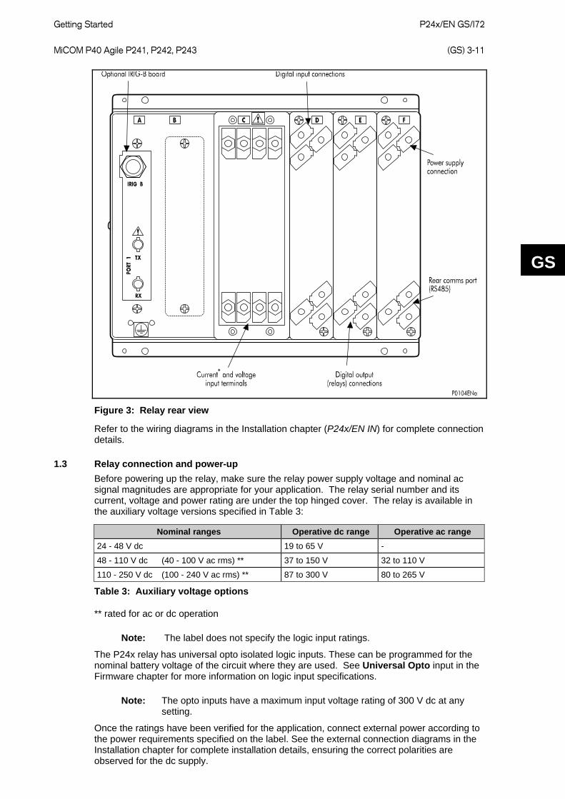
Getting Started
P24x/EN GS/I72 MiCOM P40 Agile P241, P242, P243 (GS) 3-11
GS
Figure 3: Relay rear view
Refer to the wiring diagrams in the Installation chapter (P24x/EN IN) for complete connection details.
1.3 Relay connection and power-up Before powering up the relay, make sure the relay power supply voltage and nominal ac signal magnitudes are appropriate for your application. The relay serial number and its current, voltage and power rating are under the top hinged cover. The relay is available in the auxiliary voltage versions specified in Table 3:
Nominal ranges Operative dc range Operative ac range 24 - 48 V dc 19 to 65 V -
48 - 110 V dc (40 - 100 V ac rms) ** 37 to 150 V 32 to 110 V
110 - 250 V dc (100 - 240 V ac rms) ** 87 to 300 V 80 to 265 V
Table 3: Auxiliary voltage options
** rated for ac or dc operation
Note: The label does not specify the logic input ratings.
The P24x relay has universal opto isolated logic inputs. These can be programmed for the nominal battery voltage of the circuit where they are used. See Universal Opto input in the Firmware chapter for more information on logic input specifications.
Note: The opto inputs have a maximum input voltage rating of 300 V dc at any setting.
Once the ratings have been verified for the application, connect external power according to the power requirements specified on the label. See the external connection diagrams in the Installation chapter for complete installation details, ensuring the correct polarities are observed for the dc supply.
P24x/EN GS/I72
Getting Started (GS) 3-12 MiCOM P40 Agile P241, P242, P243
GS
1.4 Introduction to the user interfaces and settings options The relay has the following user interfaces:
• The front panel using the LCD and keypad • The front port which supports Courier communication • The rear port which supports one protocol of either Courier, MODBUS or
IEC 60870-5-103. The protocol for the rear port must be specified when the relay is ordered
• A second rear port (option) which supports Courier communication The measurement information and relay settings that can be accessed from the four interfaces are summarized in Table 4.
Keypad/LCD Courier MODBUS IEC 870-5-103 Display & modification of all settings • • •
Digital I/O signal status • • • •
Display/extraction of measurements • • • •
Display/extraction of fault records • • • •
Extraction of disturbance records • • •
Programmable scheme logic settings •
Reset of fault & alarm records • • • •
Clear event & fault records • • •
Time synchronization • • •
Control commands • • • •
Table 4: Information and controls accessed from available interfaces
1.5 Menu structure The relay’s menu is arranged in a table. Each setting in the menu is known as a cell, and each cell in the menu may be accessed using a row and column address. The settings are arranged so that each column contains related settings, for example all the disturbance recorder settings are in the same column. As shown in Figure 4, the top row of each column contains the heading that describes the settings contained within that column. You can only move between the columns of the menu at the column heading level.
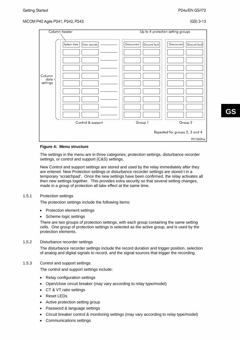
Getting Started
P24x/EN GS/I72 MiCOM P40 Agile P241, P242, P243 (GS) 3-13
GS
Figure 4: Menu structure
The settings in the menu are in three categories; protection settings, disturbance recorder settings, or control and support (C&S) settings.
New Control and support settings are stored and used by the relay immediately after they are entered. New Protection settings or disturbance recorder settings are stored t in a temporary ‘scratchpad’. Once the new settings have been confirmed, the relay activates all then new settings together. This provides extra security so that several setting changes, made in a group of protection all take effect at the same time.
1.5.1 Protection settings The protection settings include the following items:
• Protection element settings • Scheme logic settings There are two groups of protection settings, with each group containing the same setting cells. One group of protection settings is selected as the active group, and is used by the protection elements.
1.5.2 Disturbance recorder settings The disturbance recorder settings include the record duration and trigger position, selection of analog and digital signals to record, and the signal sources that trigger the recording.
1.5.3 Control and support settings The control and support settings include:
• Relay configuration settings • Open/close circuit breaker (may vary according to relay type/model) • CT & VT ratio settings • Reset LEDs • Active protection setting group • Password & language settings • Circuit breaker control & monitoring settings (may vary according to relay type/model) • Communications settings
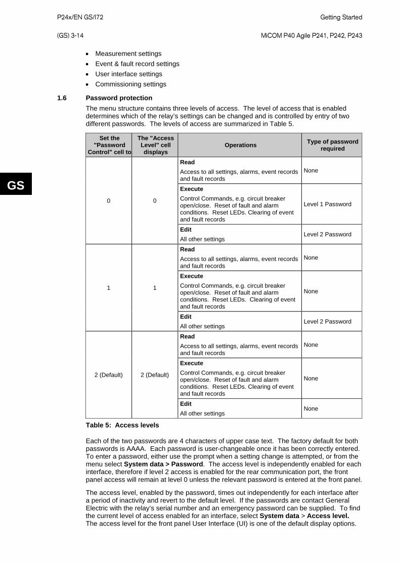
P24x/EN GS/I72
Getting Started (GS) 3-14 MiCOM P40 Agile P241, P242, P243
GS
• Measurement settings • Event & fault record settings • User interface settings • Commissioning settings
1.6 Password protection The menu structure contains three levels of access. The level of access that is enabled determines which of the relay’s settings can be changed and is controlled by entry of two different passwords. The levels of access are summarized in Table 5.
Set the "Password
Control" cell to
The "Access Level" cell displays
Operations Type of password required
0 0
Read Access to all settings, alarms, event records and fault records
None
Execute Control Commands, e.g. circuit breaker open/close. Reset of fault and alarm conditions. Reset LEDs. Clearing of event and fault records
Level 1 Password
Edit All other settings
Level 2 Password
1 1
Read Access to all settings, alarms, event records and fault records
None
Execute Control Commands, e.g. circuit breaker open/close. Reset of fault and alarm conditions. Reset LEDs. Clearing of event and fault records
None
Edit All other settings
Level 2 Password
2 (Default) 2 (Default)
Read Access to all settings, alarms, event records and fault records
None
Execute Control Commands, e.g. circuit breaker open/close. Reset of fault and alarm conditions. Reset LEDs. Clearing of event and fault records
None
Edit All other settings
None
Table 5: Access levels
Each of the two passwords are 4 characters of upper case text. The factory default for both passwords is AAAA. Each password is user-changeable once it has been correctly entered. To enter a password, either use the prompt when a setting change is attempted, or from the menu select System data > Password. The access level is independently enabled for each interface, therefore if level 2 access is enabled for the rear communication port, the front panel access will remain at level 0 unless the relevant password is entered at the front panel.
The access level, enabled by the password, times out independently for each interface after a period of inactivity and revert to the default level. If the passwords are contact General Electric with the relay’s serial number and an emergency password can be supplied. To find the current level of access enabled for an interface, select System data > Access level. The access level for the front panel User Interface (UI) is one of the default display options.
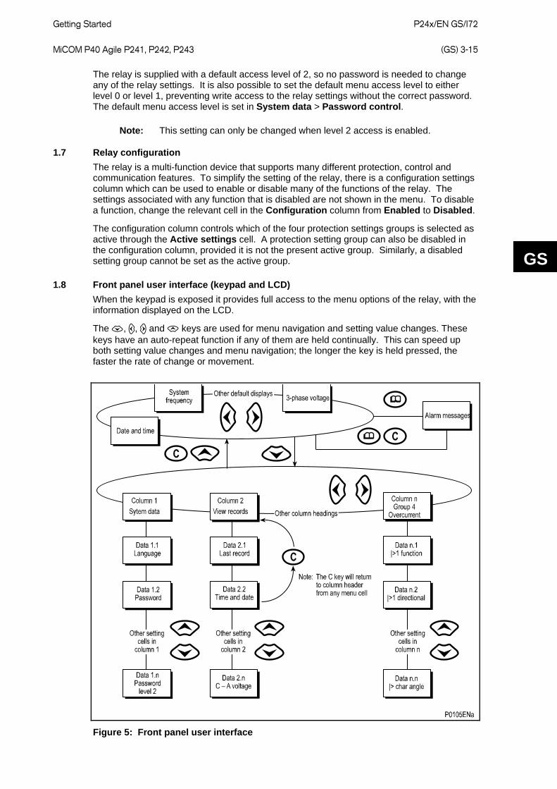
Getting Started
P24x/EN GS/I72 MiCOM P40 Agile P241, P242, P243 (GS) 3-15
GS
The relay is supplied with a default access level of 2, so no password is needed to change any of the relay settings. It is also possible to set the default menu access level to either level 0 or level 1, preventing write access to the relay settings without the correct password. The default menu access level is set in System data > Password control.
Note: This setting can only be changed when level 2 access is enabled.
1.7 Relay configuration The relay is a multi-function device that supports many different protection, control and communication features. To simplify the setting of the relay, there is a configuration settings column which can be used to enable or disable many of the functions of the relay. The settings associated with any function that is disabled are not shown in the menu. To disable a function, change the relevant cell in the Configuration column from Enabled to Disabled.
The configuration column controls which of the four protection settings groups is selected as active through the Active settings cell. A protection setting group can also be disabled in the configuration column, provided it is not the present active group. Similarly, a disabled setting group cannot be set as the active group.
1.8 Front panel user interface (keypad and LCD) When the keypad is exposed it provides full access to the menu options of the relay, with the information displayed on the LCD.
The , , and keys are used for menu navigation and setting value changes. These keys have an auto-repeat function if any of them are held continually. This can speed up both setting value changes and menu navigation; the longer the key is held pressed, the faster the rate of change or movement.
Figure 5: Front panel user interface
P24x/EN GS/I72
Getting Started (GS) 3-16 MiCOM P40 Agile P241, P242, P243
GS
1.8.1 Default display and menu time-out The front panel menu has a default display. To change it, select Measure’t. setup > default display and the following items can be selected:
• Date and time • Relay description (user defined) • Plant reference (user defined) • System frequency • 3 phase voltage • 3 phase and neutral current • Power • Thermal State From the default display you can view the other default display options using the and keys. If there is no keypad activity for 15 minutes, the default display reverts to the previous setting and the LCD backlight switches off. Any setting changes that have not been confirmed are lost and the original setting values are maintained.
Whenever there is an uncleared alarm (such as fault record, protection alarm, control alarm etc.) the default display will be replaced by the following display:
Alarms/Faults Present
Enter the menu structure of the relay from the default display, even if the display shows Alarms/Faults present message.
1.8.2 Menu navigation and setting browsing Use the four arrow keys to browse the menu, following the structure shown in Figure 4. Starting at the default display, press the key to show the first column heading.
1. Use the and keys to select the required column heading.
2. Use the and keys to view the setting data in the column
3. To return to the column header, either hold the key down or press the clear key once. It is only possible to move across columns at the column heading level.
4. To return to the default display, press the key or the key from any of the column headings. If you use the auto-repeat function of the key, you cannot go straight to the default display from one of the column cells because the auto-repeat stops at the column heading.
5. Press the key to go to the default display.
1.8.3 Hotkey menu navigation 1. To access the hotkey menu from the default display, press the key directly below the
HOTKEY text on the LCD.
2. Once in the hotkey menu, use the and keys to scroll between the available options, then use the hotkeys to control the function currently displayed.
3. If neither the and keys are pressed within 20 seconds of entering a hotkey sub menu, the relay will revert to the default display.
4. Press the clear key to return to the default menu from any page of the hotkey menu.
5. The layout of a typical page of the hotkey menu is described below:
• The top line shows the contents of the previous and next cells for easy menu navigation • The center line shows the function • The bottom line shows the options assigned to the direct access keys
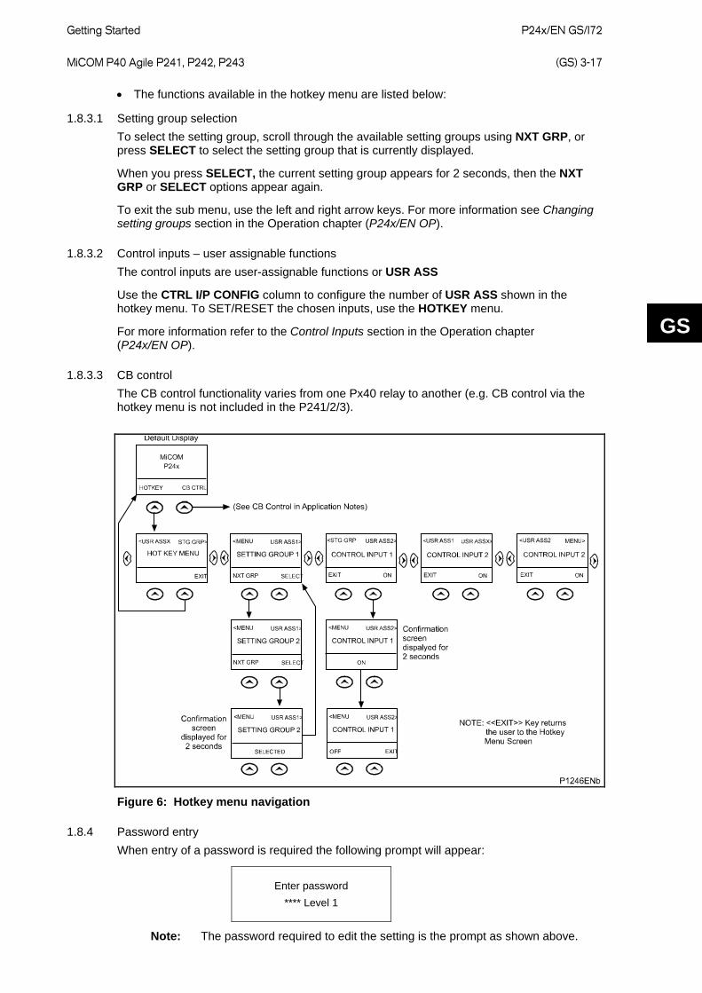
Getting Started
P24x/EN GS/I72 MiCOM P40 Agile P241, P242, P243 (GS) 3-17
GS
• The functions available in the hotkey menu are listed below:
1.8.3.1 Setting group selection To select the setting group, scroll through the available setting groups using NXT GRP, or press SELECT to select the setting group that is currently displayed.
When you press SELECT, the current setting group appears for 2 seconds, then the NXT GRP or SELECT options appear again.
To exit the sub menu, use the left and right arrow keys. For more information see Changing setting groups section in the Operation chapter (P24x/EN OP).
1.8.3.2 Control inputs – user assignable functions The control inputs are user-assignable functions or USR ASS
Use the CTRL I/P CONFIG column to configure the number of USR ASS shown in the hotkey menu. To SET/RESET the chosen inputs, use the HOTKEY menu.
For more information refer to the Control Inputs section in the Operation chapter (P24x/EN OP).
1.8.3.3 CB control The CB control functionality varies from one Px40 relay to another (e.g. CB control via the hotkey menu is not included in the P241/2/3).
Figure 6: Hotkey menu navigation
1.8.4 Password entry When entry of a password is required the following prompt will appear:
Enter password **** Level 1
Note: The password required to edit the setting is the prompt as shown above.
P24x/EN GS/I72
Getting Started (GS) 3-18 MiCOM P40 Agile P241, P242, P243
GS
A flashing cursor will indicate which character field of the password may be changed. Press the and keys to vary each character between A and Z. To move between the character fields of the password, use the and keys. The password is confirmed by pressing the enter key The display will revert to ‘Enter Password’ if an incorrect password is entered. At this point a message will be displayed indicating whether a correct password has been entered and if so what level of access has been unlocked. If this level is sufficient to edit the selected setting then the display will return to the setting page to allow the edit to continue. If the correct level of password has not been entered then the password prompt page will be returned to. To escape from this prompt press the clear key . Alternatively, the password can be entered using the ‘Password’ cell of the ‘System data’ column.
For the front panel user interface the password protected access will revert to the default access level after a keypad inactivity time-out of 15 minutes. It is possible to manually reset the password protection to the default level by moving to the Password menu cell in the System data column and pressing the clear key instead of entering a password.
1.8.5 Reading and clearing of alarm messages and fault records The presence of one or more alarm messages will be indicated by the default display and by the yellow alarm LED flashing. The alarm messages can either be self-resetting or latched, in which case they must be cleared manually. To view the alarm messages press the read key . When all alarms have been viewed, but not cleared, the alarm LED will change from flashing to constant illumination and the latest fault record will be displayed (if there is one). To scroll through the pages of this use the key. When all pages of the fault record have been viewed, the following prompt will appear:
Press clear to reset alarms
To clear all alarm messages press to return to the alarms/faults present display and leave the alarms uncleared, press . Depending on the password configuration settings, it may be necessary to enter a password before the alarm messages can be cleared (see section on password entry). When the alarms have been cleared the yellow alarm LED will extinguish, as will the red trip LED if it was illuminated following a trip.
Alternatively it is possible to accelerate the procedure, once the alarm viewer has been entered using the key, the key can be pressed, and this will move the display straight to the fault record. Pressing again will move straight to the alarm reset prompt where pressing once more will clear all alarms.
1.8.6 Setting changes To change the value of a setting, first navigate the menu to display the relevant cell. To change the cell value press the enter key which will bring up a flashing cursor on the LCD to indicate that the value can be changed. This will only happen if the appropriate password has been entered, otherwise the prompt to enter a password will appear. The setting value can then be changed by pressing the or keys. If the setting to be changed is a binary value or a text string, the required bit or character to be changed must first be selected using the and keys. When the desired new value has been reached it is confirmed as the new setting value by pressing . Alternatively, the new value will be discarded either if the clear button is pressed or if the menu time-out occurs.
For protection group settings and disturbance recorder settings, the changes must be confirmed before they are used by the relay. To do this, when all required changes have been entered, return to the column heading level and press the key. Prior to returning to the default display the following prompt will be given:
Update settings?
Enter or clear
Getting Started
P24x/EN GS/I72 MiCOM P40 Agile P241, P242, P243 (GS) 3-19
GS
Pressing will result in the new settings being adopted, pressing will cause the relay to discard the newly entered values. It should be noted that, the setting values will also be discarded if the menu time out occurs before the setting changes have been confirmed. Control and support settings will be updated immediately after they are entered, without the ‘Update settings?’ prompt.
1.9 Front communication port user interface The front communication port is provided by a 9-pin female D-type connector located under the bottom hinged cover. It provides EIA(RS)232 serial data communication and is intended for use with a PC locally to the relay (up to 15 m distance) as shown in Figure 7. This port supports the Courier communication protocol only. Courier is the communication language developed by General Electric to allow communication with its range of protection relays. The front port is particularly designed for use with the relay settings program MiCOM S1 Studio that is a Windows 98, Windows NT4.0, Windows 2000 or Windows XP based software package.
Figure 7: Front port connection
The relay is a Data Communication Equipment (DCE) device with the following pin connections on the 9-pin front port.
Pin no. 2 Tx Transmit data
Pin no. 3 Rx Receive data
Pin no. 5 0V Zero volts common
Table 6: Front port pin designation
None of the other pins are connected in the relay. The relay should be connected to the serial port of a PC, usually called COM1 or COM2. PCs are normally Data Terminal Equipment (DTE) devices which have a serial port pin connection as below (if in doubt check your PC manual):
25 way 9 way Pin no. 2 3 2 Rx Receive data
Pin no. 3 2 3 Tx Transmit data
Pin no. 5 7 5 0V Zero volts common
Table 7: DTE devices serial port pin designation
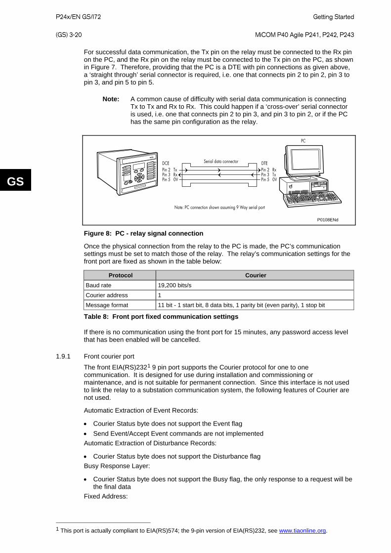
P24x/EN GS/I72
Getting Started (GS) 3-20 MiCOM P40 Agile P241, P242, P243
GS
For successful data communication, the Tx pin on the relay must be connected to the Rx pin on the PC, and the Rx pin on the relay must be connected to the Tx pin on the PC, as shown in Figure 7. Therefore, providing that the PC is a DTE with pin connections as given above, a ‘straight through’ serial connector is required, i.e. one that connects pin 2 to pin 2, pin 3 to pin 3, and pin 5 to pin 5.
Note: A common cause of difficulty with serial data communication is connecting Tx to Tx and Rx to Rx. This could happen if a ‘cross-over’ serial connector is used, i.e. one that connects pin 2 to pin 3, and pin 3 to pin 2, or if the PC has the same pin configuration as the relay.
P0108ENd
Figure 8: PC - relay signal connection
Once the physical connection from the relay to the PC is made, the PC’s communication settings must be set to match those of the relay. The relay’s communication settings for the front port are fixed as shown in the table below:
Protocol Courier Baud rate 19,200 bits/s
Courier address 1
Message format 11 bit - 1 start bit, 8 data bits, 1 parity bit (even parity), 1 stop bit
Table 8: Front port fixed communication settings
If there is no communication using the front port for 15 minutes, any password access level that has been enabled will be cancelled.
1.9.1 Front courier port The front EIA(RS)2321 9 pin port supports the Courier protocol for one to one communication. It is designed for use during installation and commissioning or maintenance, and is not suitable for permanent connection. Since this interface is not used to link the relay to a substation communication system, the following features of Courier are not used.
Automatic Extraction of Event Records:
• Courier Status byte does not support the Event flag • Send Event/Accept Event commands are not implemented Automatic Extraction of Disturbance Records:
• Courier Status byte does not support the Disturbance flag Busy Response Layer:
• Courier Status byte does not support the Busy flag, the only response to a request will be the final data
Fixed Address:
1 This port is actually compliant to EIA(RS)574; the 9-pin version of EIA(RS)232, see www.tiaonline.org.

Getting Started
P24x/EN GS/I72 MiCOM P40 Agile P241, P242, P243 (GS) 3-21
GS
• The address of the front courier port is always 1, the Change Device address command is not supported.
Fixed Baud Rate:
• 19200 bps
Note: Although automatic extraction of event and disturbance records is not supported it is possible to manually access this data via the front port.
1.10 MiCOM S1 Studio relay communications basics The EIA(RS)232 front communication port is intended for use with the relay settings program MiCOM S1 Studio. This program runs on WindowsTM 2000, XP or Vista, and is the universal MiCOM IED Support Software used for direct access to all stored data in any MiCOM IED.
MiCOM S1 Studio provides full access to:
• MiCOM Px40, Modulex series, K series, L series relays • MiCOM Mx20 measurements units
1.10.1 PC requirements To run MiCOM S1 Studio on a PC, the following requirements are advised.
• Minimum • 1 GHz processor • 256 MB RAM • WindowsTM 2000 • Resolution 800 x 600 x 256 colors • 1 GB free hard disk space
Recommended
• 2 GHz processor • 1 GB RAM • WindowsTM XP • Resolution 1024 x 768 • 5 GB free hard disk space
Microsoft WindowsTM Vista
• 2 GHz processor • 1 GB RAM • 5 GB free hard disk space • MiCOM S1 Studio must be started with Administrator rights
1.10.2 Connecting to the relay using MiCOM S1 Studio This section is intended as a quick start guide to using MiCOM S1 Studio and assumes you have a copy installed on your PC. See the MiCOM S1 Studio program online help for more detailed information.
1. Make sure the EIA(RS)232 serial cable is properly connected between the port on the front panel of the relay and the PC.
2. To start Micom S1 Studio, select Programs > MiCOM S1 Studio > MiCOM S1 Studio.
3. Click the Quick Connect tab and select Create a New System. 4. Check the Path to System file is correct, then enter the name of the system in the
Name field. If you need to add a brief description of the system, use the Comment field.
5. Click OK.

P24x/EN GS/I72
Getting Started (GS) 3-22 MiCOM P40 Agile P241, P242, P243
GS
6. Select the device type. 7. Select the communications port. 8. Once connected, select the language for the settings file, the device name, then click
Finish. The configuration is updated. 9. In the Studio Explorer window, select Device > Supervise Device… to control the
relay directly.
1.10.3 Off-line use of MiCOM S1 Studio Micom S1 Studio can also be used as an off-line tool to prepare settings, without access to the relay.
1. If creating a new system, in the Studio Explorer, select create new system. Then right-click the new system and select New substation.
2. Right-click the new substation and select New voltage level. 3. Then right-click the new voltage level and select New bay. 4. Then right-click the new bay and select New device.
You can add a device at any level, whether it is a system, substation, voltage or bay. 5. Select a device type from the list, then enter the relay type, such as P445. Click
Next. 6. Enter the full model number and click Next. 7. Select the Language and Model, then click Next. 8. Enter a unique device name, then click Finish. 9. Right-click the Settings folder and select New File. A default file 000 is added. 10. Right-click file 000 and select click Open. You can then edit the settings. See the
MiCOM S1 Studio program online help for more information.
1.11 The User Programmable Curve Tool (UPCT) The User Programmable Curve Tool allows the creation of user-defined curves and flexible download and upload of these curves into/from the MiCOM Px4x range of relays. This tool can be used to create user-programmable overcurrent and thermal operating and reset curves. For example, its user-friendly graphical user interface (GUI) allows easy creation and visualization of curves either by inputting a formula or data points.
1.11.1 Supporting software versions The UPCT is supported by software version 57 onwards for the P24x series of Motor Protection Relays.
1.11.2 Application advantages of user-programmable curves • Provide specific protection characteristics of customer schemes. • Match more closely to the withstand characteristics for electrical equipment than standard
curves. • Provide compatibility with older relays and different manufacturers relays for
retrofit/refurbishment. • Data can be exported for protection grading and testing purposes.
1.11.3 The main features and overview of the User Configurable Curve Tool: • Allows the user to create new configuration curve files or edit existing curve files • Allows the user to enter a defined number of curve points (up to 256 points) or a user-
defined formula • Allows the user to create and save multiple formulae • Allows the user-defined curve to be associated with a predefined curve Px4x template • Allows interpolation between curve points • Allows the user to save curve formulae in XML format and configured curve points in CSV
format, enabling easy data exchange • Allows the user to save template configured curve data in CRV format, suitable for
download into the relay

Getting Started
P24x/EN GS/I72 MiCOM P40 Agile P241, P242, P243 (GS) 3-23
GS
• Enables easy upload of the curve data from a relay • Allows the user to input formula constants with user-defined values • Allows the user to easily set a definite minimum time (DMT) in the formula defined curves • Graphically displays curves with zoom, pan, and point-on-curve facilities • Color coding of multiple curves enables effective comparison • Allows the user to print curves or save curves in a range of standard image formats Please refer to the User Programmable Curve Tool Guide (Px4x/EN UPCT) for more information.
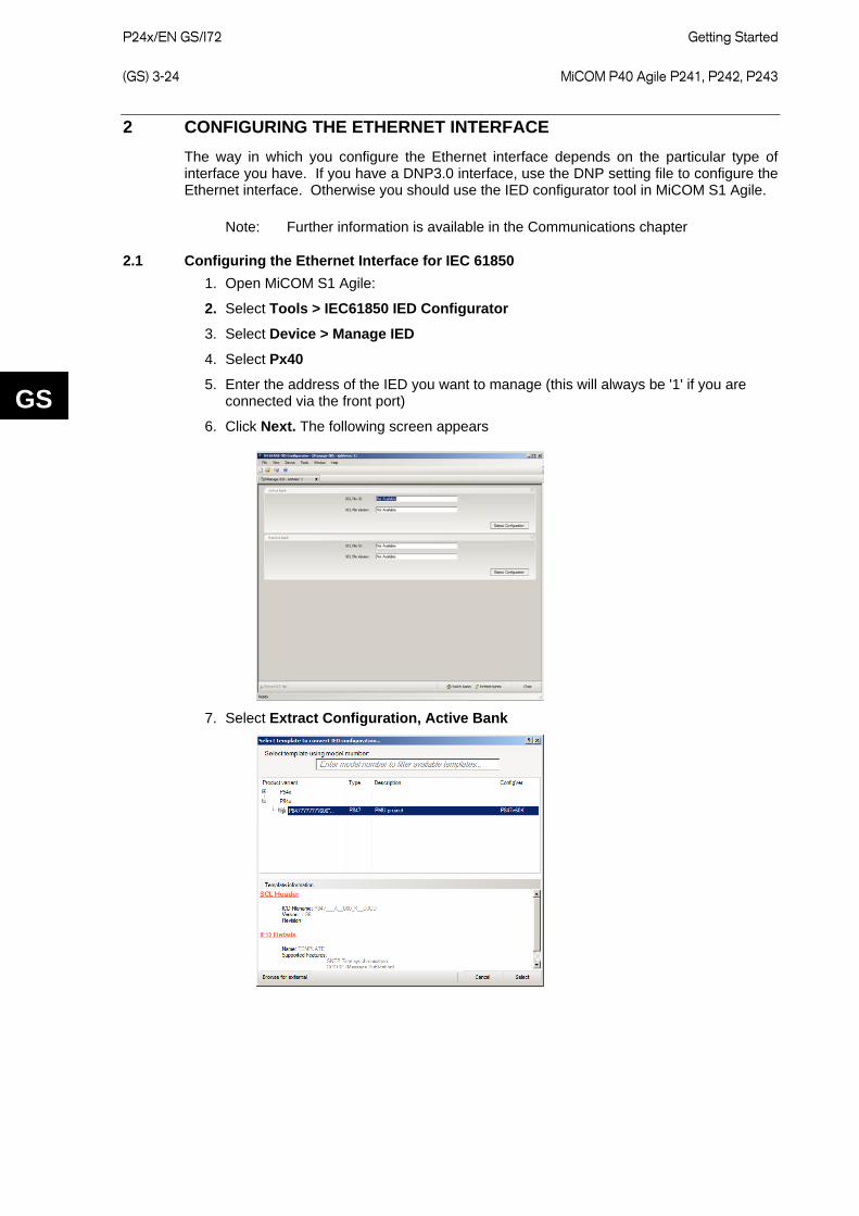
P24x/EN GS/I72
Getting Started (GS) 3-24 MiCOM P40 Agile P241, P242, P243
GS
2 CONFIGURING THE ETHERNET INTERFACE The way in which you configure the Ethernet interface depends on the particular type of interface you have. If you have a DNP3.0 interface, use the DNP setting file to configure the Ethernet interface. Otherwise you should use the IED configurator tool in MiCOM S1 Agile.
Note: Further information is available in the Communications chapter
2.1 Configuring the Ethernet Interface for IEC 61850 1. Open MiCOM S1 Agile:
2. Select Tools > IEC61850 IED Configurator
3. Select Device > Manage IED
4. Select Px40
5. Enter the address of the IED you want to manage (this will always be '1' if you are connected via the front port)
6. Click Next. The following screen appears
7. Select Extract Configuration, Active Bank
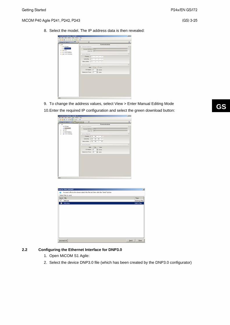
Getting Started
P24x/EN GS/I72 MiCOM P40 Agile P241, P242, P243 (GS) 3-25
GS
8. Select the model. The IP address data is then revealed:
9. To change the address values, select View > Enter Manual Editing Mode
10. Enter the required IP configuration and select the green download button:
2.2 Configuring the Ethernet Interface for DNP3.0 1. Open MiCOM S1 Agile:
2. Select the device DNP3.0 file (which has been created by the DNP3.0 configurator)
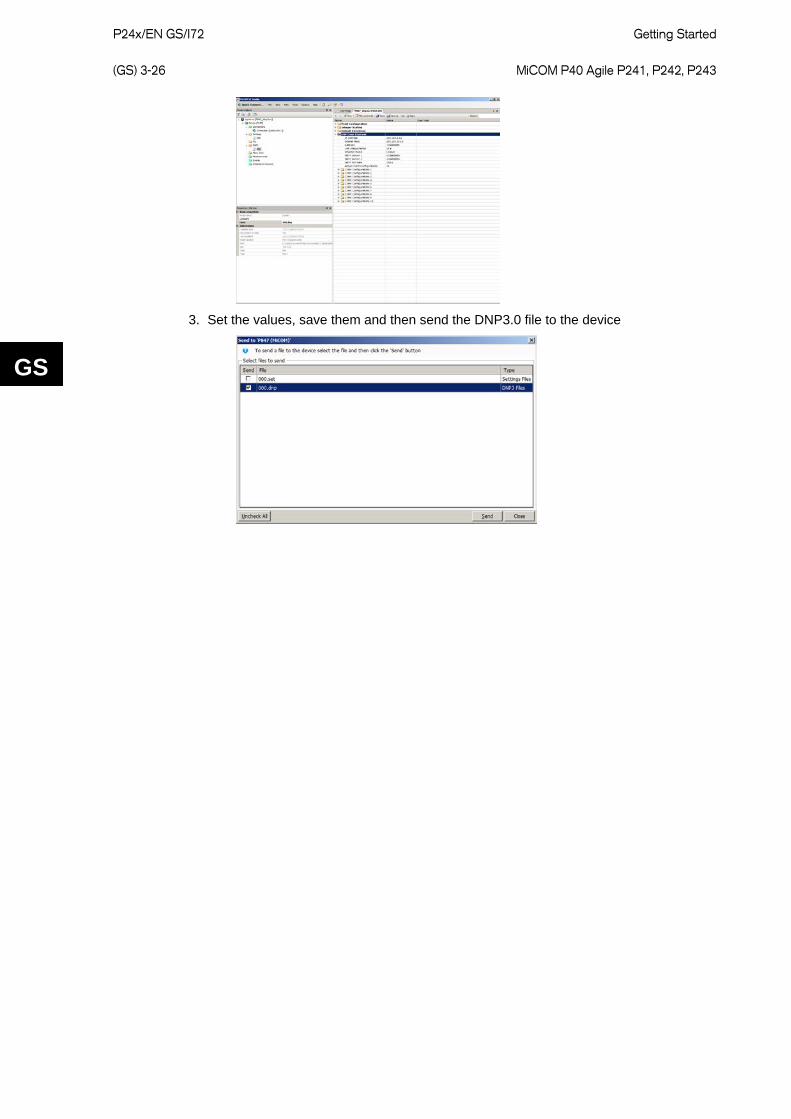
P24x/EN GS/I72
Getting Started (GS) 3-26 MiCOM P40 Agile P241, P242, P243
GS
3. Set the values, save them and then send the DNP3.0 file to the device
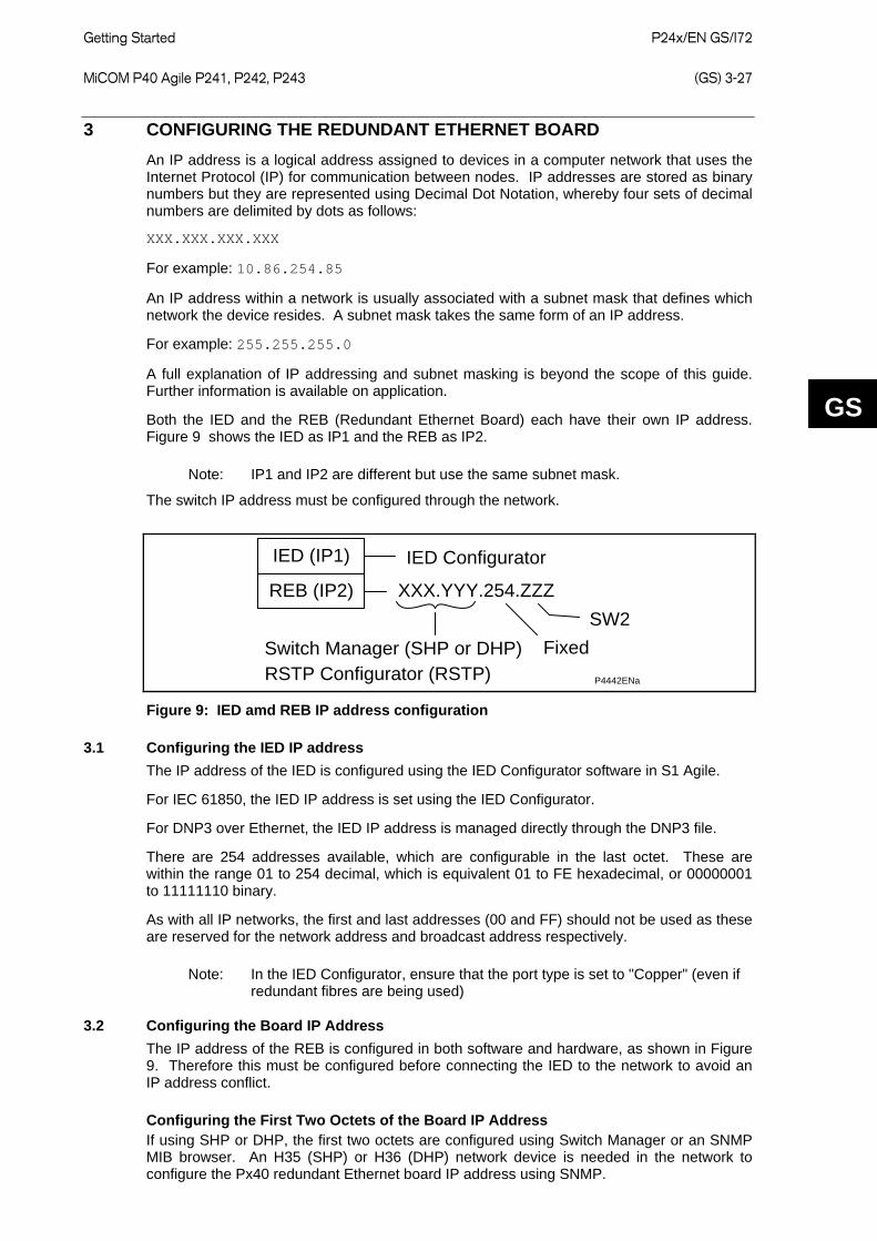
Getting Started
P24x/EN GS/I72 MiCOM P40 Agile P241, P242, P243 (GS) 3-27
GS
3 CONFIGURING THE REDUNDANT ETHERNET BOARD An IP address is a logical address assigned to devices in a computer network that uses the Internet Protocol (IP) for communication between nodes. IP addresses are stored as binary numbers but they are represented using Decimal Dot Notation, whereby four sets of decimal numbers are delimited by dots as follows:
XXX.XXX.XXX.XXX
For example: 10.86.254.85
An IP address within a network is usually associated with a subnet mask that defines which network the device resides. A subnet mask takes the same form of an IP address.
For example: 255.255.255.0
A full explanation of IP addressing and subnet masking is beyond the scope of this guide. Further information is available on application.
Both the IED and the REB (Redundant Ethernet Board) each have their own IP address. Figure 9 shows the IED as IP1 and the REB as IP2.
Note: IP1 and IP2 are different but use the same subnet mask.
The switch IP address must be configured through the network.
IED (IP1) IED Configurator
XXX.YYY.254.ZZZ
FixedSW2
Switch Manager (SHP or DHP)RSTP Configurator (RSTP)
REB (IP2)
P4442ENa
Figure 9: IED amd REB IP address configuration
3.1 Configuring the IED IP address The IP address of the IED is configured using the IED Configurator software in S1 Agile.
For IEC 61850, the IED IP address is set using the IED Configurator.
For DNP3 over Ethernet, the IED IP address is managed directly through the DNP3 file.
There are 254 addresses available, which are configurable in the last octet. These are within the range 01 to 254 decimal, which is equivalent 01 to FE hexadecimal, or 00000001 to 11111110 binary.
As with all IP networks, the first and last addresses (00 and FF) should not be used as these are reserved for the network address and broadcast address respectively.
Note: In the IED Configurator, ensure that the port type is set to "Copper" (even if redundant fibres are being used)
3.2 Configuring the Board IP Address The IP address of the REB is configured in both software and hardware, as shown in Figure 9. Therefore this must be configured before connecting the IED to the network to avoid an IP address conflict.
Configuring the First Two Octets of the Board IP Address If using SHP or DHP, the first two octets are configured using Switch Manager or an SNMP MIB browser. An H35 (SHP) or H36 (DHP) network device is needed in the network to configure the Px40 redundant Ethernet board IP address using SNMP.
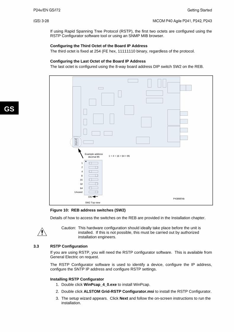
P24x/EN GS/I72
Getting Started (GS) 3-28 MiCOM P40 Agile P241, P242, P243
GS
If using Rapid Spanning Tree Protocol (RSTP), the first two octets are configured using the RSTP Configurator software tool or using an SNMP MIB browser.
Configuring the Third Octet of the Board IP Address The third octet is fixed at 254 (FE hex, 11111110 binary, regardless of the protocol.
Configuring the Last Octet of the Board IP Address The last octet is configured using the 8-way board address DIP switch SW2 on the REB.
P4389ENb
1
2
4
8
16
32
64Unused
SW2 Top view
ON
Example address decimal 85 1 + 4 + 16 + 64 = 85
Figure 10: REB address switches (SW2)
Details of how to access the switches on the REB are provided in the Installation chapter.
Caution: This hardware configuration should ideally take place before the unit is installed. If this is not possible, this must be carried out by authorized installation engineers.
3.3 RSTP Configuration If you are using RSTP, you will need the RSTP configurator software. This is available from General Electric on request.
The RSTP Configurator software is used to identify a device, configure the IP address, configure the SNTP IP address and configure RSTP settings.
Installing RSTP Configurator 1. Double click WinPcap_4_0.exe to install WinPcap.
2. Double click ALSTOM Grid-RSTP Configurator.msi to install the RSTP Configurator.
3. The setup wizard appears. Click Next and follow the on-screen instructions to run the installation.
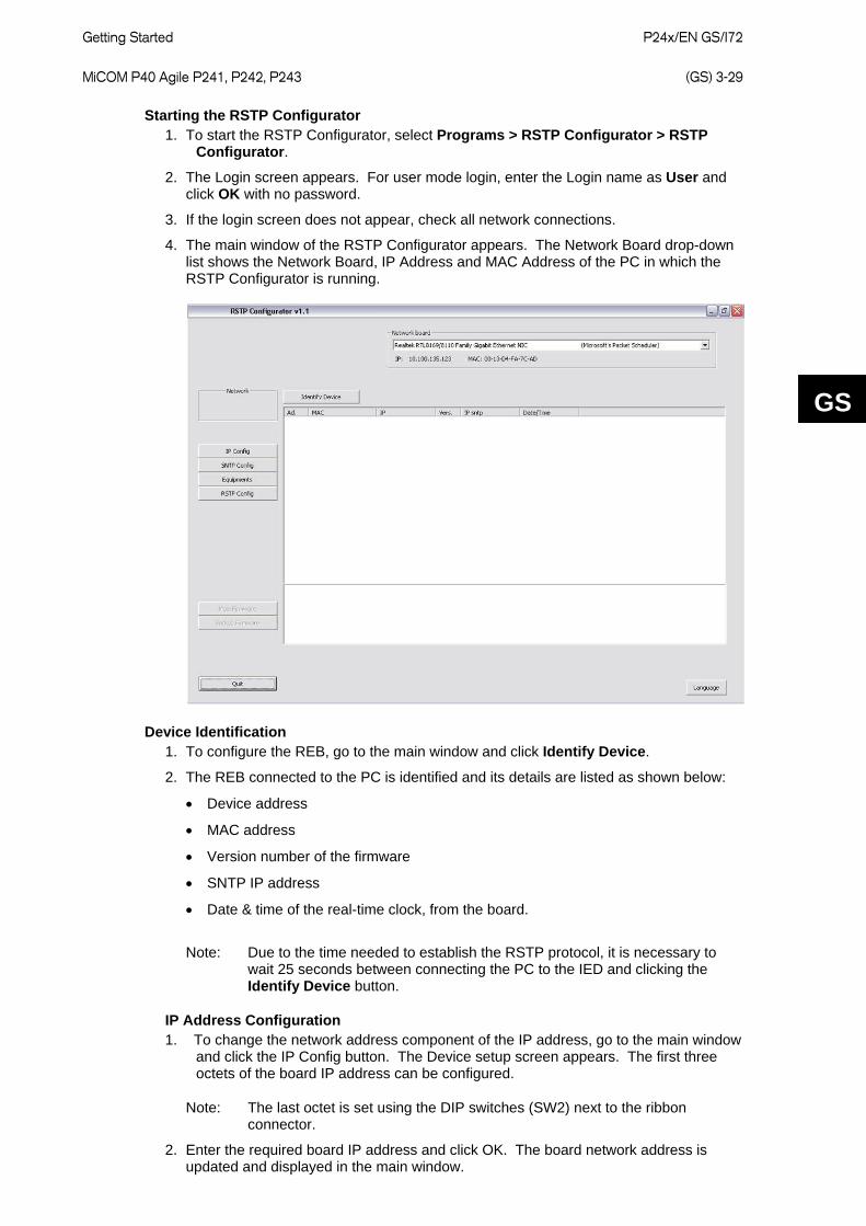
Getting Started
P24x/EN GS/I72 MiCOM P40 Agile P241, P242, P243 (GS) 3-29
GS
Starting the RSTP Configurator 1. To start the RSTP Configurator, select Programs > RSTP Configurator > RSTP
Configurator.
2. The Login screen appears. For user mode login, enter the Login name as User and click OK with no password.
3. If the login screen does not appear, check all network connections.
4. The main window of the RSTP Configurator appears. The Network Board drop-down list shows the Network Board, IP Address and MAC Address of the PC in which the RSTP Configurator is running.
Device Identification 1. To configure the REB, go to the main window and click Identify Device.
2. The REB connected to the PC is identified and its details are listed as shown below:
• Device address
• MAC address
• Version number of the firmware
• SNTP IP address
• Date & time of the real-time clock, from the board.
Note: Due to the time needed to establish the RSTP protocol, it is necessary to wait 25 seconds between connecting the PC to the IED and clicking the Identify Device button.
IP Address Configuration 1. To change the network address component of the IP address, go to the main window
and click the IP Config button. The Device setup screen appears. The first three octets of the board IP address can be configured.
Note: The last octet is set using the DIP switches (SW2) next to the ribbon connector.
2. Enter the required board IP address and click OK. The board network address is updated and displayed in the main window.
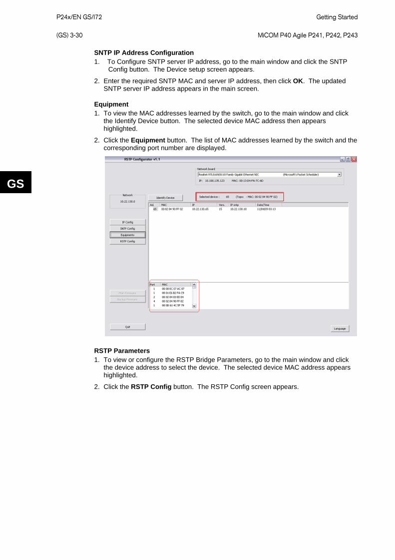
P24x/EN GS/I72
Getting Started (GS) 3-30 MiCOM P40 Agile P241, P242, P243
GS
SNTP IP Address Configuration 1. To Configure SNTP server IP address, go to the main window and click the SNTP
Config button. The Device setup screen appears.
2. Enter the required SNTP MAC and server IP address, then click OK. The updated SNTP server IP address appears in the main screen.
Equipment 1. To view the MAC addresses learned by the switch, go to the main window and click
the Identify Device button. The selected device MAC address then appears highlighted.
2. Click the Equipment button. The list of MAC addresses learned by the switch and the corresponding port number are displayed.
RSTP Parameters 1. To view or configure the RSTP Bridge Parameters, go to the main window and click
the device address to select the device. The selected device MAC address appears highlighted.
2. Click the RSTP Config button. The RSTP Config screen appears.
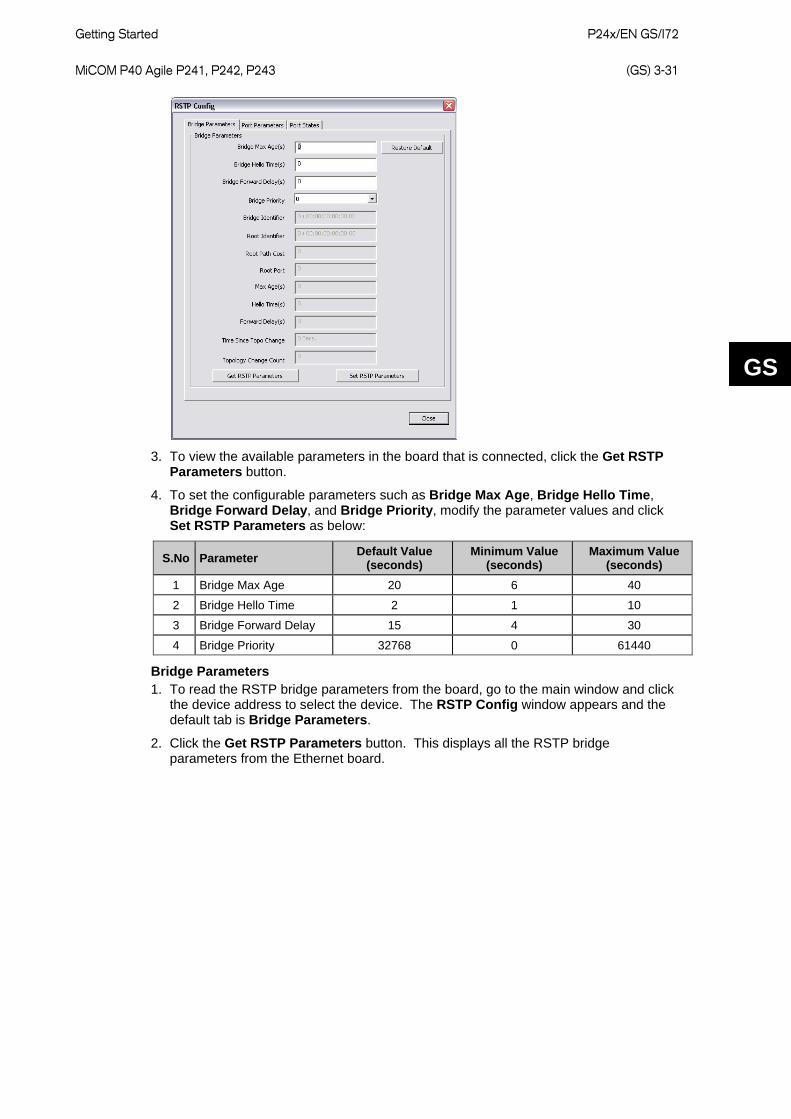
Getting Started
P24x/EN GS/I72 MiCOM P40 Agile P241, P242, P243 (GS) 3-31
GS
3. To view the available parameters in the board that is connected, click the Get RSTP
Parameters button.
4. To set the configurable parameters such as Bridge Max Age, Bridge Hello Time, Bridge Forward Delay, and Bridge Priority, modify the parameter values and click Set RSTP Parameters as below:
S.No Parameter Default Value (seconds)
Minimum Value (seconds)
Maximum Value (seconds)
1 Bridge Max Age 20 6 40
2 Bridge Hello Time 2 1 10
3 Bridge Forward Delay 15 4 30
4 Bridge Priority 32768 0 61440
Bridge Parameters 1. To read the RSTP bridge parameters from the board, go to the main window and click
the device address to select the device. The RSTP Config window appears and the default tab is Bridge Parameters.
2. Click the Get RSTP Parameters button. This displays all the RSTP bridge parameters from the Ethernet board.
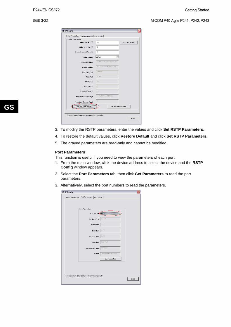
P24x/EN GS/I72
Getting Started (GS) 3-32 MiCOM P40 Agile P241, P242, P243
GS
3. To modify the RSTP parameters, enter the values and click Set RSTP Parameters.
4. To restore the default values, click Restore Default and click Set RSTP Parameters.
5. The grayed parameters are read-only and cannot be modified.
Port Parameters This function is useful if you need to view the parameters of each port. 1. From the main window, click the device address to select the device and the RSTP
Config window appears.
2. Select the Port Parameters tab, then click Get Parameters to read the port parameters.
3. Alternatively, select the port numbers to read the parameters.
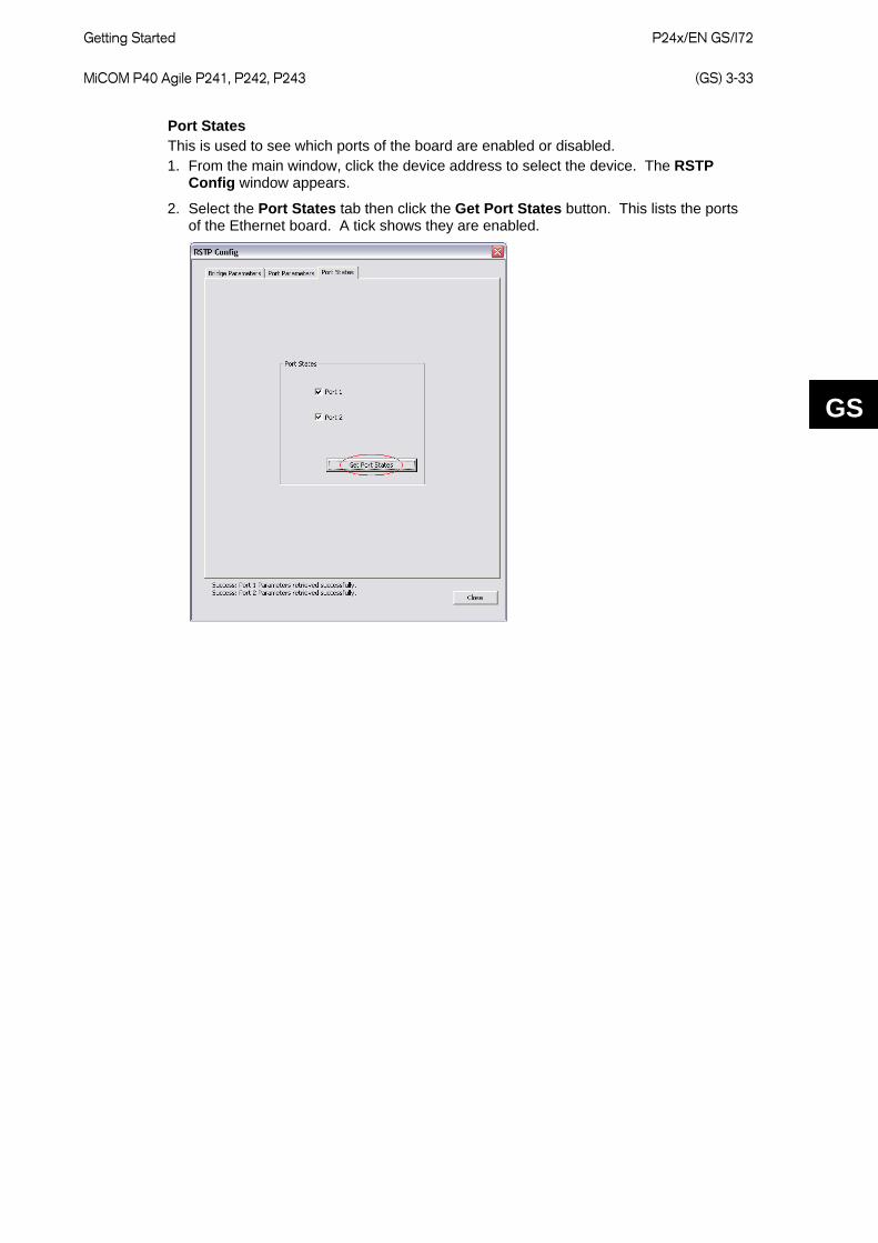
Getting Started
P24x/EN GS/I72 MiCOM P40 Agile P241, P242, P243 (GS) 3-33
GS
Port States This is used to see which ports of the board are enabled or disabled. 1. From the main window, click the device address to select the device. The RSTP
Config window appears.
2. Select the Port States tab then click the Get Port States button. This lists the ports of the Ethernet board. A tick shows they are enabled.
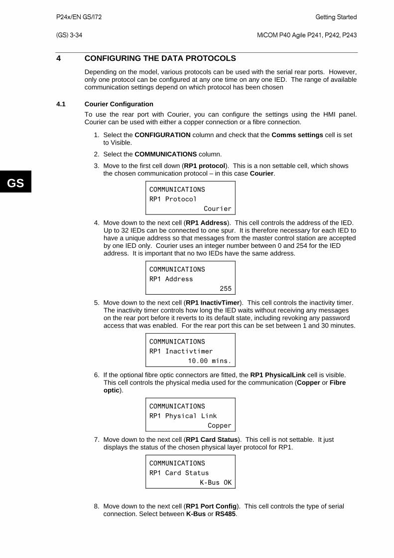
P24x/EN GS/I72
Getting Started (GS) 3-34 MiCOM P40 Agile P241, P242, P243
GS
4 CONFIGURING THE DATA PROTOCOLS Depending on the model, various protocols can be used with the serial rear ports. However, only one protocol can be configured at any one time on any one IED. The range of available communication settings depend on which protocol has been chosen
4.1 Courier Configuration To use the rear port with Courier, you can configure the settings using the HMI panel. Courier can be used with either a copper connection or a fibre connection.
1. Select the CONFIGURATION column and check that the Comms settings cell is set to Visible.
2. Select the COMMUNICATIONS column.
3. Move to the first cell down (RP1 protocol). This is a non settable cell, which shows the chosen communication protocol – in this case Courier.
COMMUNICATIONS RP1 Protocol
Courier
4. Move down to the next cell (RP1 Address). This cell controls the address of the IED. Up to 32 IEDs can be connected to one spur. It is therefore necessary for each IED to have a unique address so that messages from the master control station are accepted by one IED only. Courier uses an integer number between 0 and 254 for the IED address. It is important that no two IEDs have the same address.
COMMUNICATIONS RP1 Address
255
5. Move down to the next cell (RP1 InactivTimer). This cell controls the inactivity timer. The inactivity timer controls how long the IED waits without receiving any messages on the rear port before it reverts to its default state, including revoking any password access that was enabled. For the rear port this can be set between 1 and 30 minutes.
COMMUNICATIONS RP1 Inactivtimer
10.00 mins.
6. If the optional fibre optic connectors are fitted, the RP1 PhysicalLink cell is visible. This cell controls the physical media used for the communication (Copper or Fibre optic).
COMMUNICATIONS RP1 Physical Link
Copper
7. Move down to the next cell (RP1 Card Status). This cell is not settable. It just displays the status of the chosen physical layer protocol for RP1.
COMMUNICATIONS RP1 Card Status
K-Bus OK
8. Move down to the next cell (RP1 Port Config). This cell controls the type of serial
connection. Select between K-Bus or RS485.
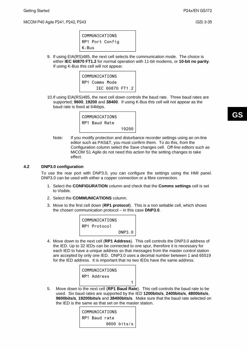
Getting Started
P24x/EN GS/I72 MiCOM P40 Agile P241, P242, P243 (GS) 3-35
GS
COMMUNICATIONS RP1 Port Config
K-Bus
9. If using EIA(RS)485, the next cell selects the communication mode. The choice is either IEC 60870 FT1.2 for normal operation with 11-bit modems, or 10-bit no parity. If using K-Bus this cell will not appear.
COMMUNICATIONS RP1 Comms Mode
IEC 60870 FT1.2
10. If using EIA(RS)485, the next cell down controls the baud rate. Three baud rates are supported; 9600, 19200 and 38400. If using K-Bus this cell will not appear as the baud rate is fixed at 64kbps.
COMMUNICATIONS RP1 Baud Rate
19200
Note: If you modify protection and disturbance recorder settings using an on-line editor such as PAS&T, you must confirm them. To do this, from the Configuration column select the Save changes cell. Off-line editors such as MiCOM S1 Agile do not need this action for the setting changes to take effect.
4.2 DNP3.0 configuration To use the rear port with DNP3.0, you can configure the settings using the HMI panel. DNP3.0 can be used with either a copper connection or a fibre connection.
1. Select the CONFIGURATION column and check that the Comms settings cell is set to Visible.
2. Select the COMMUNICATIONS column.
3. Move to the first cell down (RP1 protocol). This is a non settable cell, which shows the chosen communication protocol – in this case DNP3.0.
COMMUNICATIONS RP1 Protocol
DNP3.0
4. Move down to the next cell (RP1 Address). This cell controls the DNP3.0 address of the IED. Up to 32 IEDs can be connected to one spur, therefore it is necessary for each IED to have a unique address so that messages from the master control station are accepted by only one IED. DNP3.0 uses a decimal number between 1 and 65519 for the IED address. It is important that no two IEDs have the same address.
COMMUNICATIONS RP1 Address
1 5. Move down to the next cell (RP1 Baud Rate). This cell controls the baud rate to be
used. Six baud rates are supported by the IED 1200bits/s, 2400bits/s, 4800bits/s, 9600bits/s, 19200bits/s and 38400bits/s. Make sure that the baud rate selected on the IED is the same as that set on the master station.
COMMUNICATIONS RP1 Baud rate
9600 bits/s
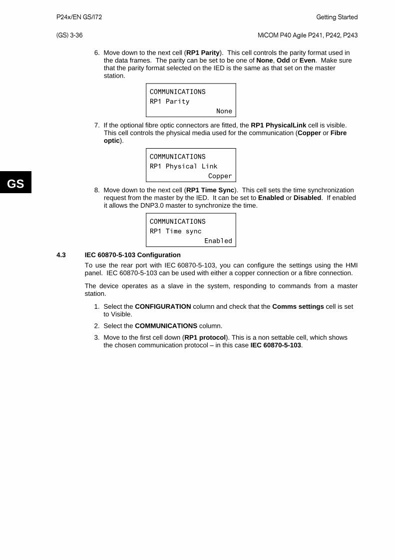
P24x/EN GS/I72
Getting Started (GS) 3-36 MiCOM P40 Agile P241, P242, P243
GS
6. Move down to the next cell (RP1 Parity). This cell controls the parity format used in the data frames. The parity can be set to be one of None, Odd or Even. Make sure that the parity format selected on the IED is the same as that set on the master station.
COMMUNICATIONS RP1 Parity
None
7. If the optional fibre optic connectors are fitted, the RP1 PhysicalLink cell is visible. This cell controls the physical media used for the communication (Copper or Fibre optic).
COMMUNICATIONS RP1 Physical Link
Copper
8. Move down to the next cell (RP1 Time Sync). This cell sets the time synchronization request from the master by the IED. It can be set to Enabled or Disabled. If enabled it allows the DNP3.0 master to synchronize the time.
COMMUNICATIONS RP1 Time sync
Enabled
4.3 IEC 60870-5-103 Configuration To use the rear port with IEC 60870-5-103, you can configure the settings using the HMI panel. IEC 60870-5-103 can be used with either a copper connection or a fibre connection.
The device operates as a slave in the system, responding to commands from a master station.
1. Select the CONFIGURATION column and check that the Comms settings cell is set to Visible.
2. Select the COMMUNICATIONS column.
3. Move to the first cell down (RP1 protocol). This is a non settable cell, which shows the chosen communication protocol – in this case IEC 60870-5-103.
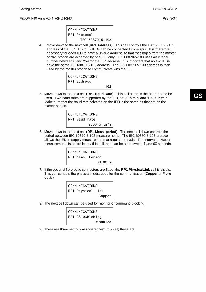
Getting Started
P24x/EN GS/I72 MiCOM P40 Agile P241, P242, P243 (GS) 3-37
GS
COMMUNICATIONS RP1 Protocol
IEC 60870-5-103 4. Move down to the next cell (RP1 Address). This cell controls the IEC 60870-5-103
address of the IED. Up to 32 IEDs can be connected to one spur. It is therefore necessary for each IED to have a unique address so that messages from the master control station are accepted by one IED only. IEC 60870-5-103 uses an integer number between 0 and 254 for the IED address. It is important that no two IEDs have the same IEC 60870 5 103 address. The IEC 60870-5-103 address is then used by the master station to communicate with the IED.
COMMUNICATIONS RP1 address
162
5. Move down to the next cell (RP1 Baud Rate). This cell controls the baud rate to be used. Two baud rates are supported by the IED, ‘9600 bits/s’ and ‘19200 bits/s’. Make sure that the baud rate selected on the IED is the same as that set on the master station.
COMMUNICATIONS RP1 Baud rate
9600 bits/s
6. Move down to the next cell (RP1 Meas. period). The next cell down controls the period between IEC 60870-5-103 measurements. The IEC 60870-5-103 protocol allows the IED to supply measurements at regular intervals. The interval between measurements is controlled by this cell, and can be set between 1 and 60 seconds.
COMMUNICATIONS RP1 Meas. Period
30.00 s
7. If the optional fibre optic connectors are fitted, the RP1 PhysicalLink cell is visible. This cell controls the physical media used for the communication (Copper or Fibre optic).
COMMUNICATIONS RP1 Physical Link
Copper
8. The next cell down can be used for monitor or command blocking.
COMMUNICATIONS RP1 CS103Blcking
Disabled
9. There are three settings associated with this cell; these are:
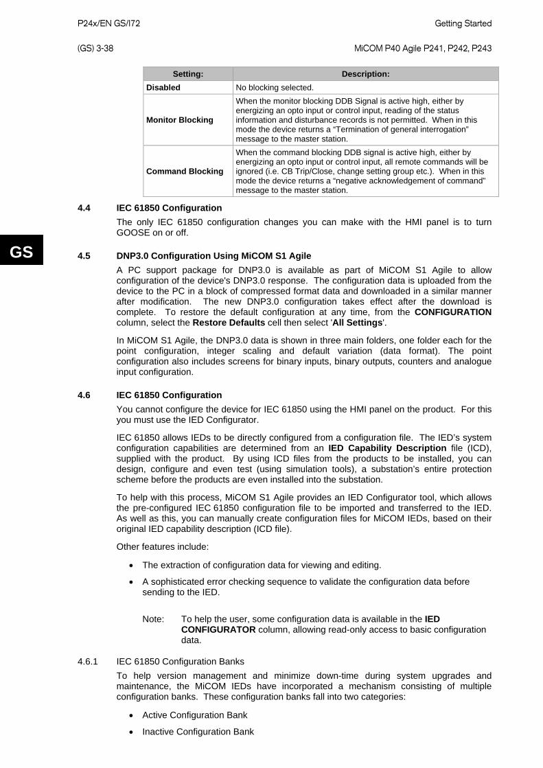
P24x/EN GS/I72
Getting Started (GS) 3-38 MiCOM P40 Agile P241, P242, P243
GS
Setting: Description: Disabled No blocking selected.
Monitor Blocking
When the monitor blocking DDB Signal is active high, either by energizing an opto input or control input, reading of the status information and disturbance records is not permitted. When in this mode the device returns a “Termination of general interrogation” message to the master station.
Command Blocking
When the command blocking DDB signal is active high, either by energizing an opto input or control input, all remote commands will be ignored (i.e. CB Trip/Close, change setting group etc.). When in this mode the device returns a “negative acknowledgement of command” message to the master station.
4.4 IEC 61850 Configuration The only IEC 61850 configuration changes you can make with the HMI panel is to turn GOOSE on or off.
4.5 DNP3.0 Configuration Using MiCOM S1 Agile A PC support package for DNP3.0 is available as part of MiCOM S1 Agile to allow configuration of the device's DNP3.0 response. The configuration data is uploaded from the device to the PC in a block of compressed format data and downloaded in a similar manner after modification. The new DNP3.0 configuration takes effect after the download is complete. To restore the default configuration at any time, from the CONFIGURATION column, select the Restore Defaults cell then select 'All Settings'.
In MiCOM S1 Agile, the DNP3.0 data is shown in three main folders, one folder each for the point configuration, integer scaling and default variation (data format). The point configuration also includes screens for binary inputs, binary outputs, counters and analogue input configuration.
4.6 IEC 61850 Configuration You cannot configure the device for IEC 61850 using the HMI panel on the product. For this you must use the IED Configurator.
IEC 61850 allows IEDs to be directly configured from a configuration file. The IED’s system configuration capabilities are determined from an IED Capability Description file (ICD), supplied with the product. By using ICD files from the products to be installed, you can design, configure and even test (using simulation tools), a substation’s entire protection scheme before the products are even installed into the substation.
To help with this process, MiCOM S1 Agile provides an IED Configurator tool, which allows the pre-configured IEC 61850 configuration file to be imported and transferred to the IED. As well as this, you can manually create configuration files for MiCOM IEDs, based on their original IED capability description (ICD file).
Other features include:
• The extraction of configuration data for viewing and editing.
• A sophisticated error checking sequence to validate the configuration data before sending to the IED.
Note: To help the user, some configuration data is available in the IED CONFIGURATOR column, allowing read-only access to basic configuration data.
4.6.1 IEC 61850 Configuration Banks To help version management and minimize down-time during system upgrades and maintenance, the MiCOM IEDs have incorporated a mechanism consisting of multiple configuration banks. These configuration banks fall into two categories:
• Active Configuration Bank
• Inactive Configuration Bank
Getting Started
P24x/EN GS/I72 MiCOM P40 Agile P241, P242, P243 (GS) 3-39
GS
Any new configuration sent to the IED is automatically stored in the inactive configuration bank, therefore not immediately affecting the current configuration.
When the upgrade or maintenance stage is complete, the IED Configurator tool can be used to transmit a command, which authorizes activation of the new configuration contained in the inactive configuration bank. This is done by switching the active and inactive configuration banks. The capability of switching the configuration banks is also available using the IED CONFIGURATOR column of the HMI.
The SCL Name and Revision attributes of both configuration banks are also available in the IED CONFIGURATOR column of the HMI.
4.6.2 IEC 61850 Network Connectivity Configuration of the IP parameters and SNTP time synchronization parameters is performed by the IED Configurator tool. If these parameters are not available using an SCL file, they must be configured manually.
As the IP addressing will be completely detached and independent from any public network, it is up to the company’s system administrator to establish the IP addressing strategy. Every IP address on the network must be unique. This applies to all devices on the network. Duplicate IP addresses will result in conflict and must be avoided. The IED will check for a conflict on every IP configuration change and at power up. An alarm will be raised if an IP conflict is detected.
The IED can be configured to accept data from other networks using the Gateway setting. If multiple networks are used, the IP addresses must be unique across networks.
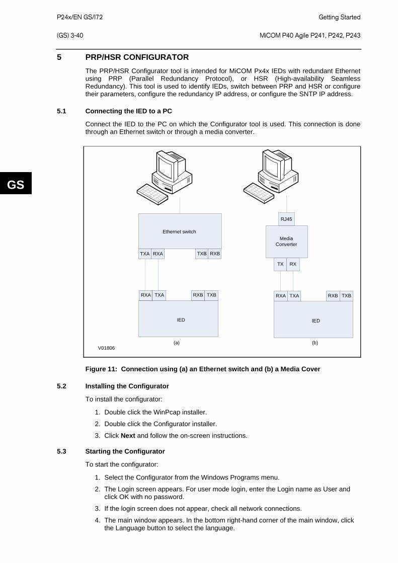
P24x/EN GS/I72
Getting Started (GS) 3-40 MiCOM P40 Agile P241, P242, P243
GS
5 PRP/HSR CONFIGURATOR The PRP/HSR Configurator tool is intended for MiCOM Px4x IEDs with redundant Ethernet using PRP (Parallel Redundancy Protocol), or HSR (High-availability Seamless Redundancy). This tool is used to identify IEDs, switch between PRP and HSR or configure their parameters, configure the redundancy IP address, or configure the SNTP IP address.
5.1 Connecting the IED to a PC
Connect the IED to the PC on which the Configurator tool is used. This connection is done through an Ethernet switch or through a media converter.
IED
Ethernet switch
TXA
Media Converter
RJ45
V01806
RXA TXB RXB
RXA TXA RXB TXB
TX RX
(a) (b)
IED
RXA TXA RXB TXB
Figure 11: Connection using (a) an Ethernet switch and (b) a Media Cover
5.2 Installing the Configurator
To install the configurator:
1. Double click the WinPcap installer.
2. Double click the Configurator installer.
3. Click Next and follow the on-screen instructions.
5.3 Starting the Configurator
To start the configurator:
1. Select the Configurator from the Windows Programs menu.
2. The Login screen appears. For user mode login, enter the Login name as User and click OK with no password.
3. If the login screen does not appear, check all network connections.
4. The main window appears. In the bottom right-hand corner of the main window, click the Language button to select the language.
Getting Started
P24x/EN GS/I72 MiCOM P40 Agile P241, P242, P243 (GS) 3-41
GS
5. The Network Board drop-down list shows the Network Board, IP Address and MAC Address of the
6. PC in which the Configurator is running.
5.4 PRP/HSR device identification
To configure the redundant Ethernet board, go to the main window and click the Identify Device button. A list of devices are shown with the following details:
1. Device address
2. MAC address
3. Version number of the firmware
4. SNTP IP address
5. Date & time of the real-time clock, from the board.
Select the device you wish to configure. The MAC address of the selected device is highlighted.
5.5 Selecting the device mode
You must now select the device mode that you wish to use. This will be either PRP or HSR. To do this, select the appropriate radio button then click the Update button. You will be asked to confirm a device reboot. Click OK to confirm.
5.6 PRP/HSR IP Address Configuration
To change the network address component of the IP address:
1. From the main window click the IP Config button. The Device setup screen appears.
2. Enter the required board IP address and click OK. This is the redundancy network address, not the IEC 61850 IP address.
3. The board network address is updated and displayed in the main window.
5.7 SNTP IP Address Configuration
To Configure the SNTP server IP address:
1. From the main window click the SNTP Config button. The Device setup screen appears.
2. Enter the required MAC SNTP address and server IP SNTP Address. Click OK.
3. The updated MAC and IP SNTP addresses appear in the main screen.
5.8 Check for connected equipment
To check what devices are connected to the device being monitored:
1. From the main window, select the device.
2. Click the Equipment button.
3. At the bottom of the main window, a box shows the ports where devices are connected and their MAC addresses.
5.9 PRP Configuration
To view or configure the PRP Parameters:
1. Ensure that you have set the device mode to PRP.
2. Click the PRP/HSR Config button. The PRP Config screen appears.
3. To view the available parameters, click the Get PRP Parameters button.
4. To change the parameters, click the Set Parameters button and modify their values.
P24x/EN GS/I72
Getting Started (GS) 3-42 MiCOM P40 Agile P241, P242, P243
GS
If you need to restore the default values of the parameters, click the Restore Defaults button.
The configurable parameters are as follows:
• Multicast Address: Use this field to configure the multicast destination address. All DANPs in the network must be configured to operate with the same multicast address for the purpose of network supervision.
• Node Forget Time: This is the time after which a node entry is cleared in the nodes table.
• Life Check Interval: This defines how often a node sends a PRP_Supervision frame. All DANPs shall be configured with the same Life Check Interval.
5.10 HSR Configuration
To view or configure the HSR Parameters:
1. Click the PRP/HSR Config button. The HSR Config screen appears.
2. To view the available parameters in the board that is connected, click the Retrieve HSR Parameters from IED button.
3. To change the parameters, click the Set Parameters button and modify their values.
If you need to restore the default values of the parameters, click the Restore Defaults button.
The configurable parameters are as follows:
• Multicast Address: Use this field to configure the multicast destination address. All DANPs in the network must be configured to operate with the same multicast address for the purpose of network supervision.
• Node Forget Time: This is the time after which a node entry is cleared in the nodes table.
• Life Check Interval: This defines how often a node sends a PRP_Supervision frame. All DANPs must be configured with the same Life Check Interval.
• Proxy Node Table Forget Time: This is the time after which a node entry is cleared in the ProxyTable
• Proxy Node Table Max Entries: This is the maximum number of entries in the ProxyTable
• Entry Forget Time: This is the time after which an entry is removed from the duplicates
• Node Reboot Interval: This is the minimum time during which a node that reboots remains silent
5.11 Filtering Database
The Filtering Database is used to determine how frames are forwarded or filtered across the on-board Ethernet switch. Filtering information specifies the set of ports to which frames received from a specific port are forwarded. The Ethernet switch examines each received frame to see if the frame's destination address matches a source address listed in the Filtering Database. If there is a match, the device uses the filtering/ forwarding information for that source address to determine how to forward or filter the frame. Otherwise the frame is forwarded to all the ports in the Ethernet switch (broadcast).
General tab The Filtering Database contains two types of entry; static and dynamic. The Static Entries are the source addresses entered by an administrator. The Dynamic Entries are the source addresses learnt by the switch process. The Dynamic Entries are removed from the Filtering Database after the Ageing Time. The Database holds a maximum of 1024 entries.
Getting Started
P24x/EN GS/I72 MiCOM P40 Agile P241, P242, P243 (GS) 3-43
GS
1. To access the forwarding database functions, if required, click the Filtering Database button in the main window.
2. To view the Forwarding Database Size, Number of Static Entries and Number of Dynamic Entries, click Read Database Info.
3. To set the Aging Time, enter the number of seconds in the text box and click the Set button.
Filtering Entries tab The Filtering Database configuration pages are used to view, add or delete entries from the Filtering Database. This feature is available only for the administrator. This Filtering Database is mainly used during the testing to verify the PRP/HSR functionality. To add an entry in the forwarding database, click the Filtering Entries tab. Configure as follows:
1. Select the Port Number and MAC Address
2. Set the Entry type (Dynamic or Static)
3. Set the cast type (Unicast or Multicast)
4. Set theMGMT and Rate Limit
5. Click the Create button. The new entry appears in the forwarding database.
To delete an entry from the forwarding database, select the entry and click the Delete Entry button.
Goose Filtering tab This page configures the source MACs from which GOOSE messages will be allowed or blocked. The filtering can be configured by either the MAC address range boxes or by selecting or unselecting the individual MAC addresses in the MAC table. After you have defined the addresses to be allowed or blocked you need to update the table and apply the filter:
• Update Table: This updates the MAC table according to the filtering range entered in the MAC address range boxes.
• Apply Filter: This applies the filtering configuration in the MAC table to the HSR/PRP board.
5.12 End of session
To finish the session:
1. In the main window, click the Quit button, a new screen appears.
2. If a database backup is required, click Yes, a new screen appears.
3. Click the ... button to browse the path. Enter the name in the text box.

P24x/EN GS/I72
Getting Started (GS) 3-44 MiCOM P40 Agile P241, P242, P243
GS
Settings
P24x/EN ST/I72 MiCOM P40 Agile P241, P242, P243 (ST) 4-1
ST
SETTINGS

P24x/EN ST/I72
Settings (ST) 4-2 MiCOM P40 Agile P241, P242, P243
ST
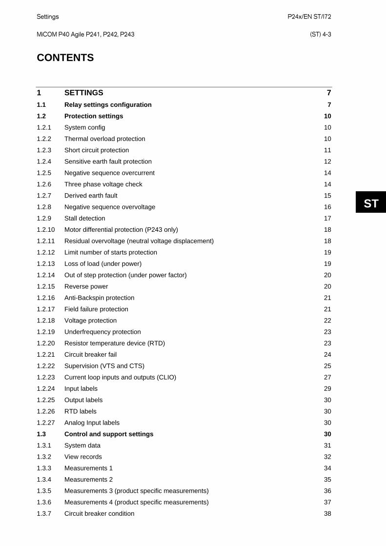
Settings
P24x/EN ST/I72 MiCOM P40 Agile P241, P242, P243 (ST) 4-3
ST
CONTENTS
1 SETTINGS 7
1.1 Relay settings configuration 7
1.2 Protection settings 10
1.2.1 System config 10
1.2.2 Thermal overload protection 10
1.2.3 Short circuit protection 11
1.2.4 Sensitive earth fault protection 12
1.2.5 Negative sequence overcurrent 14
1.2.6 Three phase voltage check 14
1.2.7 Derived earth fault 15
1.2.8 Negative sequence overvoltage 16
1.2.9 Stall detection 17
1.2.10 Motor differential protection (P243 only) 18
1.2.11 Residual overvoltage (neutral voltage displacement) 18
1.2.12 Limit number of starts protection 19
1.2.13 Loss of load (under power) 19
1.2.14 Out of step protection (under power factor) 20
1.2.15 Reverse power 20
1.2.16 Anti-Backspin protection 21
1.2.17 Field failure protection 21
1.2.18 Voltage protection 22
1.2.19 Underfrequency protection 23
1.2.20 Resistor temperature device (RTD) 23
1.2.21 Circuit breaker fail 24
1.2.22 Supervision (VTS and CTS) 25
1.2.23 Current loop inputs and outputs (CLIO) 27
1.2.24 Input labels 29
1.2.25 Output labels 30
1.2.26 RTD labels 30
1.2.27 Analog Input labels 30
1.3 Control and support settings 30
1.3.1 System data 31
1.3.2 View records 32
1.3.3 Measurements 1 34
1.3.4 Measurements 2 35
1.3.5 Measurements 3 (product specific measurements) 36
1.3.6 Measurements 4 (product specific measurements) 37
1.3.7 Circuit breaker condition 38
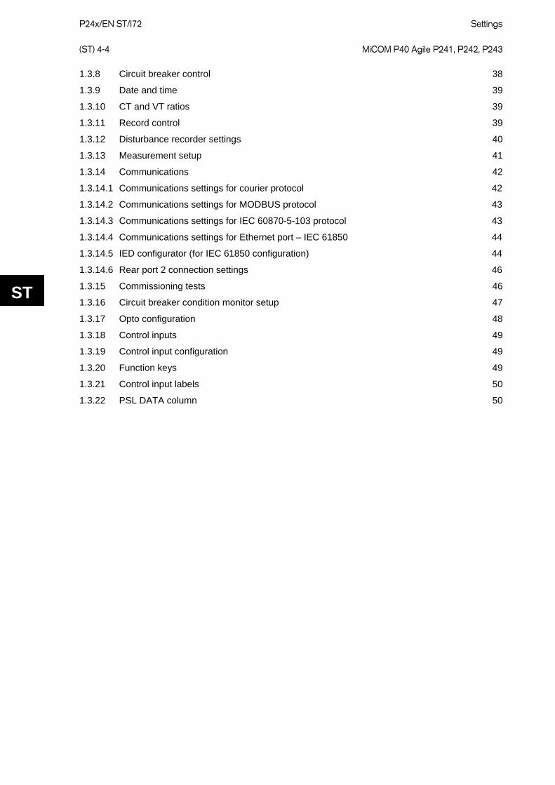
P24x/EN ST/I72
Settings (ST) 4-4 MiCOM P40 Agile P241, P242, P243
ST
1.3.8 Circuit breaker control 38
1.3.9 Date and time 39
1.3.10 CT and VT ratios 39
1.3.11 Record control 39
1.3.12 Disturbance recorder settings 40
1.3.13 Measurement setup 41
1.3.14 Communications 42
1.3.14.1 Communications settings for courier protocol 42
1.3.14.2 Communications settings for MODBUS protocol 43
1.3.14.3 Communications settings for IEC 60870-5-103 protocol 43
1.3.14.4 Communications settings for Ethernet port – IEC 61850 44
1.3.14.5 IED configurator (for IEC 61850 configuration) 44
1.3.14.6 Rear port 2 connection settings 46
1.3.15 Commissioning tests 46
1.3.16 Circuit breaker condition monitor setup 47
1.3.17 Opto configuration 48
1.3.18 Control inputs 49
1.3.19 Control input configuration 49
1.3.20 Function keys 49
1.3.21 Control input labels 50
1.3.22 PSL DATA column 50
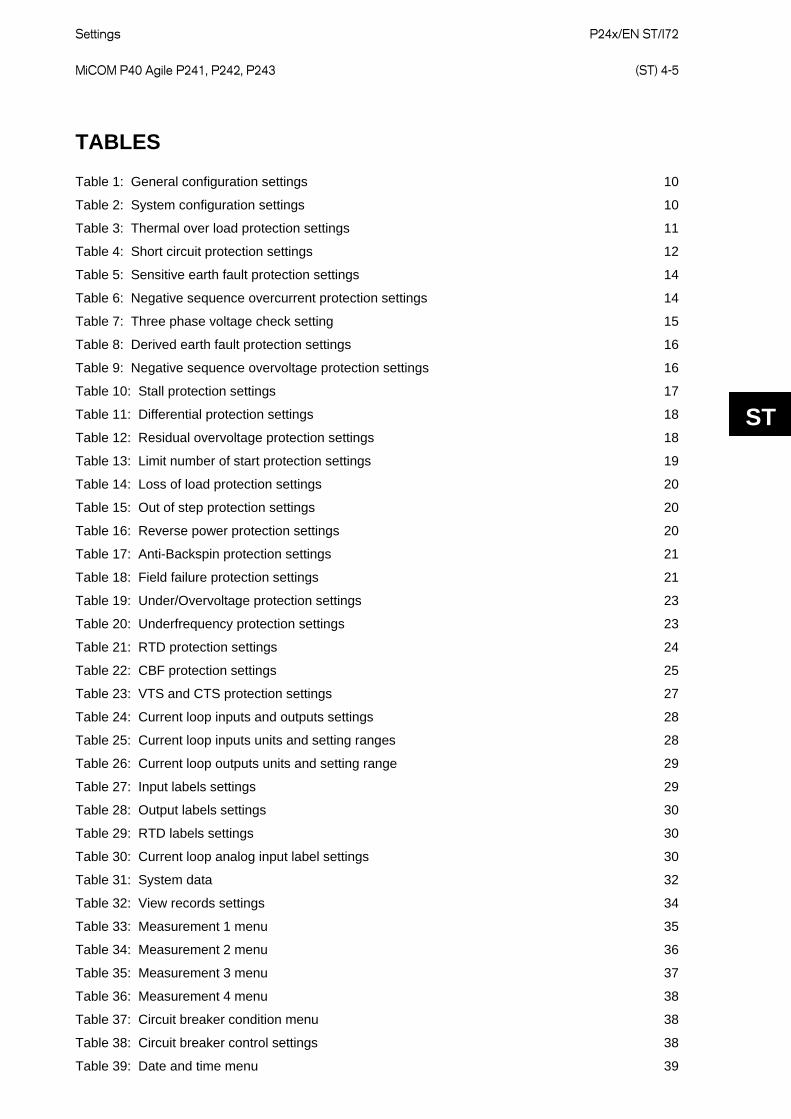
Settings
P24x/EN ST/I72 MiCOM P40 Agile P241, P242, P243 (ST) 4-5
ST
TABLES Table 1: General configuration settings 10 Table 2: System configuration settings 10 Table 3: Thermal over load protection settings 11 Table 4: Short circuit protection settings 12 Table 5: Sensitive earth fault protection settings 14 Table 6: Negative sequence overcurrent protection settings 14 Table 7: Three phase voltage check setting 15 Table 8: Derived earth fault protection settings 16 Table 9: Negative sequence overvoltage protection settings 16 Table 10: Stall protection settings 17 Table 11: Differential protection settings 18 Table 12: Residual overvoltage protection settings 18 Table 13: Limit number of start protection settings 19 Table 14: Loss of load protection settings 20 Table 15: Out of step protection settings 20 Table 16: Reverse power protection settings 20 Table 17: Anti-Backspin protection settings 21 Table 18: Field failure protection settings 21 Table 19: Under/Overvoltage protection settings 23 Table 20: Underfrequency protection settings 23 Table 21: RTD protection settings 24 Table 22: CBF protection settings 25 Table 23: VTS and CTS protection settings 27 Table 24: Current loop inputs and outputs settings 28 Table 25: Current loop inputs units and setting ranges 28 Table 26: Current loop outputs units and setting range 29 Table 27: Input labels settings 29 Table 28: Output labels settings 30 Table 29: RTD labels settings 30 Table 30: Current loop analog input label settings 30 Table 31: System data 32 Table 32: View records settings 34 Table 33: Measurement 1 menu 35 Table 34: Measurement 2 menu 36 Table 35: Measurement 3 menu 37 Table 36: Measurement 4 menu 38 Table 37: Circuit breaker condition menu 38 Table 38: Circuit breaker control settings 38 Table 39: Date and time menu 39
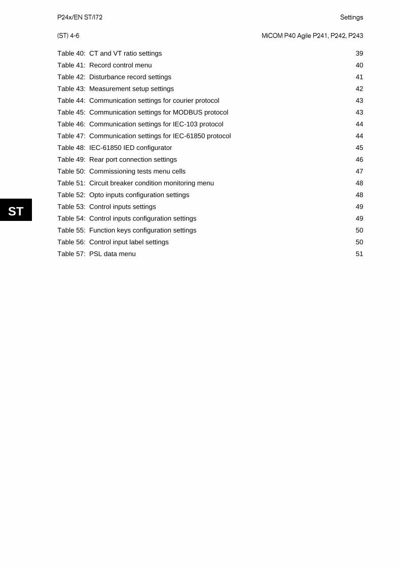
P24x/EN ST/I72
Settings (ST) 4-6 MiCOM P40 Agile P241, P242, P243
ST
Table 40: CT and VT ratio settings 39 Table 41: Record control menu 40 Table 42: Disturbance record settings 41 Table 43: Measurement setup settings 42 Table 44: Communication settings for courier protocol 43 Table 45: Communication settings for MODBUS protocol 43 Table 46: Communication settings for IEC-103 protocol 44 Table 47: Communication settings for IEC-61850 protocol 44 Table 48: IEC-61850 IED configurator 45 Table 49: Rear port connection settings 46 Table 50: Commissioning tests menu cells 47 Table 51: Circuit breaker condition monitoring menu 48 Table 52: Opto inputs configuration settings 48 Table 53: Control inputs settings 49 Table 54: Control inputs configuration settings 49 Table 55: Function keys configuration settings 50 Table 56: Control input label settings 50 Table 57: PSL data menu 51

Settings
P24x/EN ST/I72 MiCOM P40 Agile P241, P242, P243 (ST) 4-7
ST
1 SETTINGS The P241/2/3 must be configured to the system and application using appropriate settings. In this chapter the settings are described in the sequence: protection settings, control and configuration settings and the disturbance recorder settings. The relay is supplied with a factory-set configuration of default settings.
1.1 Relay settings configuration The relay is a multi-function device that supports many different protection, control and communication features. To simplify the setting of the relay, there is a configuration settings column, used to enable or disable many of the relay functions. The settings associated with any disabled function are not shown in the menu. To disable a function, change the relevant cell in the Configuration column from Enabled to Disabled.
The configuration column controls which of the two protection settings groups is selected as active through the Active settings cell. A protection setting group can also be disabled in the configuration column, provided it is not the present active group. Similarly, a disabled setting group cannot be set as the active group.
The configuration column also allows all of the setting values in one group of protection settings to be copied to another group.
To do this first set the Copy from cell to the protection setting group to be copied, then set the copy to cell to the protection group where the copy is to be placed. The copied settings are initially placed in a temporary scratchpad and will only be used by the relay following confirmation.
To restore the default values to the settings in any protection settings group, set the restore defaults cell to the relevant group number. It is possible to set the restore defaults cell to all settings to restore the default values to all of the relay’s settings, not just the protection groups’ settings. The default settings are initially placed in the scratchpad and are only used by the relay after they have been confirmed.
Note: If you restore defaults to all settings, it includes the rear communication port settings. If the new (default) settings do not match those of the master station, rear port communication may be disrupted
Menu text Default setting Available settings
Restore Defaults No Operation
No Operation All Settings Setting Group 1 Setting Group 2
Setting to restore a setting group to factory default settings.
Setting Group Select via Menu Select via Menu Select via Optos
Allows setting group changes to be initiated via opto inputs via Setting Group DDB signal in the programmable scheme logic or via the Menu settings.
Active Settings Group 1 Group 1, Group 2
Selects the active setting group.
Save Changes No Operation No Operation, Save, Abort
Saves all relay settings.
Copy from Group 1 Group 1, 2
Allows displayed settings to be copied from a selected setting group.
System Config Visible Invisible or Visible
Sets the System Config menu visible further on in the relay settings menu.
Copy to No Operation No Operation Group 1, 2
Allows displayed settings to be copied to a selected setting group. (ready to paste).
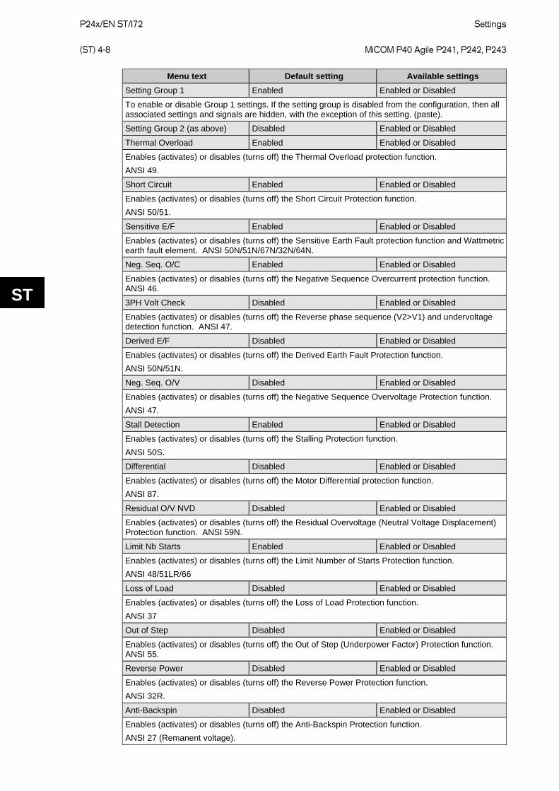
P24x/EN ST/I72
Settings (ST) 4-8 MiCOM P40 Agile P241, P242, P243
ST
Menu text Default setting Available settings Setting Group 1 Enabled Enabled or Disabled
To enable or disable Group 1 settings. If the setting group is disabled from the configuration, then all associated settings and signals are hidden, with the exception of this setting. (paste).
Setting Group 2 (as above) Disabled Enabled or Disabled
Thermal Overload Enabled Enabled or Disabled
Enables (activates) or disables (turns off) the Thermal Overload protection function. ANSI 49.
Short Circuit Enabled Enabled or Disabled
Enables (activates) or disables (turns off) the Short Circuit Protection function. ANSI 50/51.
Sensitive E/F Enabled Enabled or Disabled
Enables (activates) or disables (turns off) the Sensitive Earth Fault protection function and Wattmetric earth fault element. ANSI 50N/51N/67N/32N/64N.
Neg. Seq. O/C Enabled Enabled or Disabled
Enables (activates) or disables (turns off) the Negative Sequence Overcurrent protection function. ANSI 46.
3PH Volt Check Disabled Enabled or Disabled
Enables (activates) or disables (turns off) the Reverse phase sequence (V2>V1) and undervoltage detection function. ANSI 47.
Derived E/F Disabled Enabled or Disabled
Enables (activates) or disables (turns off) the Derived Earth Fault Protection function. ANSI 50N/51N.
Neg. Seq. O/V Disabled Enabled or Disabled
Enables (activates) or disables (turns off) the Negative Sequence Overvoltage Protection function. ANSI 47.
Stall Detection Enabled Enabled or Disabled
Enables (activates) or disables (turns off) the Stalling Protection function. ANSI 50S.
Differential Disabled Enabled or Disabled
Enables (activates) or disables (turns off) the Motor Differential protection function. ANSI 87.
Residual O/V NVD Disabled Enabled or Disabled
Enables (activates) or disables (turns off) the Residual Overvoltage (Neutral Voltage Displacement) Protection function. ANSI 59N.
Limit Nb Starts Enabled Enabled or Disabled
Enables (activates) or disables (turns off) the Limit Number of Starts Protection function. ANSI 48/51LR/66
Loss of Load Disabled Enabled or Disabled
Enables (activates) or disables (turns off) the Loss of Load Protection function. ANSI 37
Out of Step Disabled Enabled or Disabled
Enables (activates) or disables (turns off) the Out of Step (Underpower Factor) Protection function. ANSI 55.
Reverse Power Disabled Enabled or Disabled
Enables (activates) or disables (turns off) the Reverse Power Protection function. ANSI 32R.
Anti-Backspin Disabled Enabled or Disabled
Enables (activates) or disables (turns off) the Anti-Backspin Protection function. ANSI 27 (Remanent voltage).
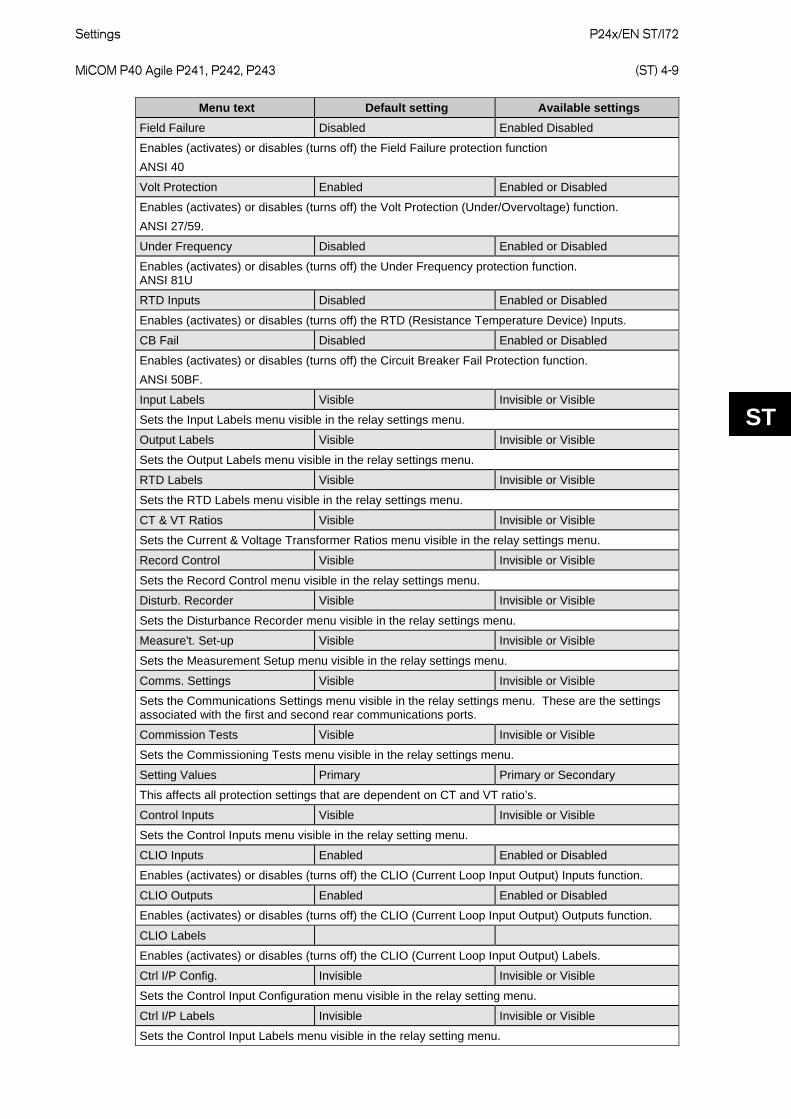
Settings
P24x/EN ST/I72 MiCOM P40 Agile P241, P242, P243 (ST) 4-9
ST
Menu text Default setting Available settings Field Failure Disabled Enabled Disabled
Enables (activates) or disables (turns off) the Field Failure protection function ANSI 40
Volt Protection Enabled Enabled or Disabled
Enables (activates) or disables (turns off) the Volt Protection (Under/Overvoltage) function. ANSI 27/59.
Under Frequency Disabled Enabled or Disabled
Enables (activates) or disables (turns off) the Under Frequency protection function. ANSI 81U
RTD Inputs Disabled Enabled or Disabled
Enables (activates) or disables (turns off) the RTD (Resistance Temperature Device) Inputs.
CB Fail Disabled Enabled or Disabled
Enables (activates) or disables (turns off) the Circuit Breaker Fail Protection function. ANSI 50BF.
Input Labels Visible Invisible or Visible
Sets the Input Labels menu visible in the relay settings menu.
Output Labels Visible Invisible or Visible
Sets the Output Labels menu visible in the relay settings menu.
RTD Labels Visible Invisible or Visible
Sets the RTD Labels menu visible in the relay settings menu.
CT & VT Ratios Visible Invisible or Visible
Sets the Current & Voltage Transformer Ratios menu visible in the relay settings menu.
Record Control Visible Invisible or Visible
Sets the Record Control menu visible in the relay settings menu.
Disturb. Recorder Visible Invisible or Visible
Sets the Disturbance Recorder menu visible in the relay settings menu.
Measure't. Set-up Visible Invisible or Visible
Sets the Measurement Setup menu visible in the relay settings menu.
Comms. Settings Visible Invisible or Visible
Sets the Communications Settings menu visible in the relay settings menu. These are the settings associated with the first and second rear communications ports.
Commission Tests Visible Invisible or Visible
Sets the Commissioning Tests menu visible in the relay settings menu.
Setting Values Primary Primary or Secondary
This affects all protection settings that are dependent on CT and VT ratio’s.
Control Inputs Visible Invisible or Visible
Sets the Control Inputs menu visible in the relay setting menu.
CLIO Inputs Enabled Enabled or Disabled
Enables (activates) or disables (turns off) the CLIO (Current Loop Input Output) Inputs function.
CLIO Outputs Enabled Enabled or Disabled
Enables (activates) or disables (turns off) the CLIO (Current Loop Input Output) Outputs function.
CLIO Labels
Enables (activates) or disables (turns off) the CLIO (Current Loop Input Output) Labels.
Ctrl I/P Config. Invisible Invisible or Visible
Sets the Control Input Configuration menu visible in the relay setting menu.
Ctrl I/P Labels Invisible Invisible or Visible
Sets the Control Input Labels menu visible in the relay setting menu.
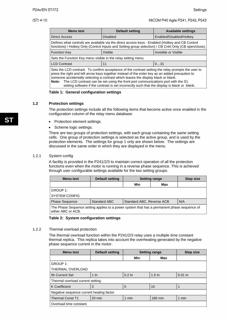
P24x/EN ST/I72
Settings (ST) 4-10 MiCOM P40 Agile P241, P242, P243
ST
Menu text Default setting Available settings Direct Access Disabled Enabled/Disabled/Hotkey
Defines what controls are available via the direct access keys - Enabled (Hotkey and CB Control functions) / Hotkey Only (Control Inputs and Setting group selection) / CB Cntrl Only (CB open/close).
Function Key Visible Invisible or Visible
Sets the Function Key menu visible in the relay setting menu.
LCD Contrast 11 0…31
Sets the LCD contrast. To confirm acceptance of the contrast setting the relay prompts the user to press the right and left arrow keys together instead of the enter key as an added precaution to someone accidentally selecting a contrast which leaves the display black or blank. Note: The LCD contrast can be set using the front port communications port with the S1 setting software if the contrast is set incorrectly such that the display is black or blank.
Table 1: General configuration settings
1.2 Protection settings The protection settings include all the following items that become active once enabled in the configuration column of the relay menu database:
• Protection element settings. • Scheme logic settings. There are two groups of protection settings, with each group containing the same setting cells. One group of protection settings is selected as the active group, and is used by the protection elements. The settings for group 1 only are shown below. The settings are discussed in the same order in which they are displayed in the menu.
1.2.1 System config A facility is provided in the P241/2/3 to maintain correct operation of all the protection functions even when the motor is running in a reverse phase sequence. This is achieved through user configurable settings available for the two setting groups.
Menu text Default setting Setting range Step size Min Max
GROUP 1: SYSTEM CONFIG
Phase Sequence Standard ABC Standard ABC, Reverse ACB N/A
The Phase Sequence setting applies to a power system that has a permanent phase sequence of either ABC or ACB.
Table 2: System configuration settings
1.2.2 Thermal overload protection The thermal overload function within the P241/2/3 relay uses a multiple time constant thermal replica. This replica takes into account the overheating generated by the negative phase sequence current in the motor.
Menu text Default setting Setting range Step size Min Max
GROUP 1: THERMAL OVERLOAD
Ith Current Set 1 In 0.2 In 1.5 In 0.01 In
Thermal overload current setting.
K Coefficient 3 0 10 1
Negative sequence current heating factor.
Thermal Const T1 20 min 1 min 180 min 1 min
Overload time constant.
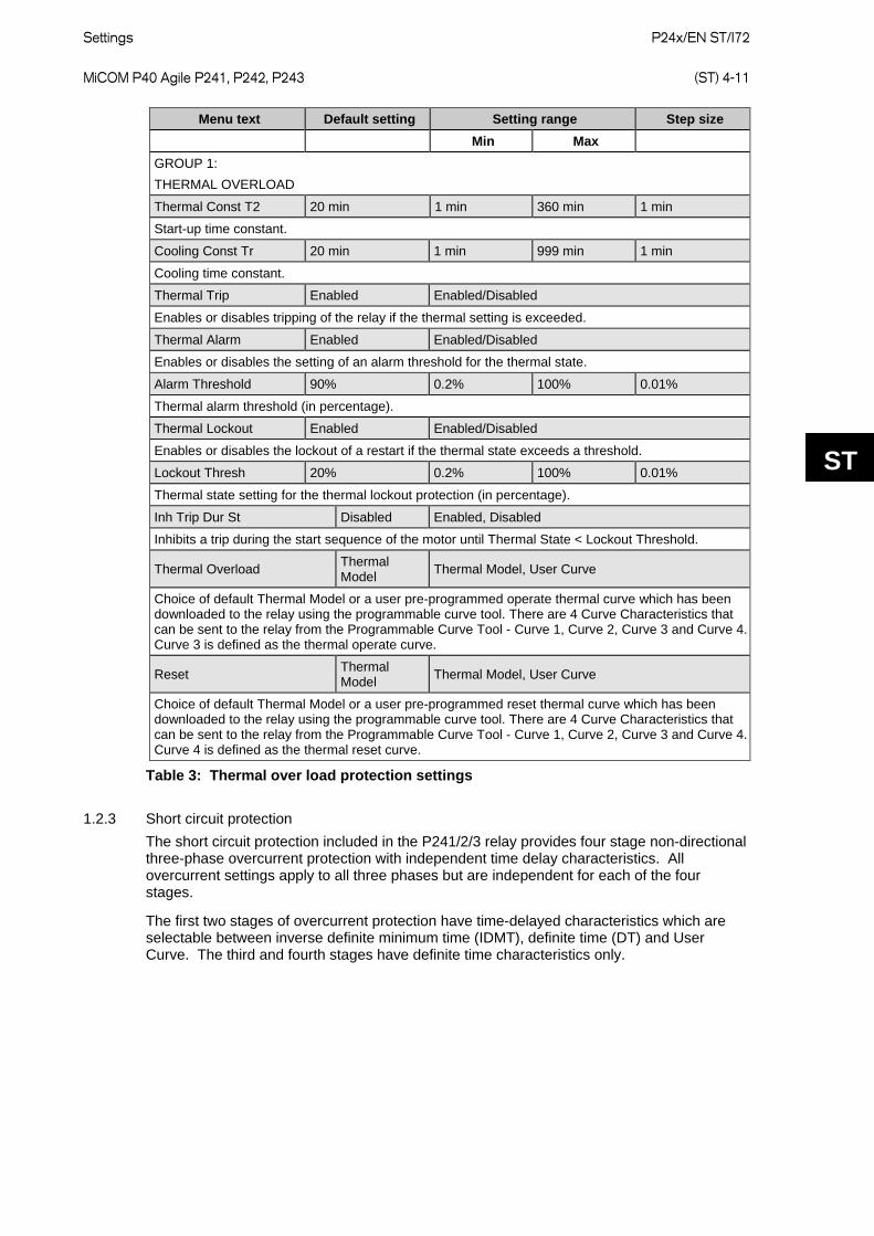
Settings
P24x/EN ST/I72 MiCOM P40 Agile P241, P242, P243 (ST) 4-11
ST
Menu text Default setting Setting range Step size Min Max
GROUP 1: THERMAL OVERLOAD
Thermal Const T2 20 min 1 min 360 min 1 min
Start-up time constant.
Cooling Const Tr 20 min 1 min 999 min 1 min
Cooling time constant.
Thermal Trip Enabled Enabled/Disabled
Enables or disables tripping of the relay if the thermal setting is exceeded.
Thermal Alarm Enabled Enabled/Disabled
Enables or disables the setting of an alarm threshold for the thermal state.
Alarm Threshold 90% 0.2% 100% 0.01%
Thermal alarm threshold (in percentage).
Thermal Lockout Enabled Enabled/Disabled
Enables or disables the lockout of a restart if the thermal state exceeds a threshold.
Lockout Thresh 20% 0.2% 100% 0.01%
Thermal state setting for the thermal lockout protection (in percentage).
Inh Trip Dur St Disabled Enabled, Disabled
Inhibits a trip during the start sequence of the motor until Thermal State < Lockout Threshold.
Thermal Overload Thermal Model Thermal Model, User Curve
Choice of default Thermal Model or a user pre-programmed operate thermal curve which has been downloaded to the relay using the programmable curve tool. There are 4 Curve Characteristics that can be sent to the relay from the Programmable Curve Tool - Curve 1, Curve 2, Curve 3 and Curve 4. Curve 3 is defined as the thermal operate curve.
Reset Thermal Model Thermal Model, User Curve
Choice of default Thermal Model or a user pre-programmed reset thermal curve which has been downloaded to the relay using the programmable curve tool. There are 4 Curve Characteristics that can be sent to the relay from the Programmable Curve Tool - Curve 1, Curve 2, Curve 3 and Curve 4. Curve 4 is defined as the thermal reset curve.
Table 3: Thermal over load protection settings
1.2.3 Short circuit protection The short circuit protection included in the P241/2/3 relay provides four stage non-directional three-phase overcurrent protection with independent time delay characteristics. All overcurrent settings apply to all three phases but are independent for each of the four stages.
The first two stages of overcurrent protection have time-delayed characteristics which are selectable between inverse definite minimum time (IDMT), definite time (DT) and User Curve. The third and fourth stages have definite time characteristics only.
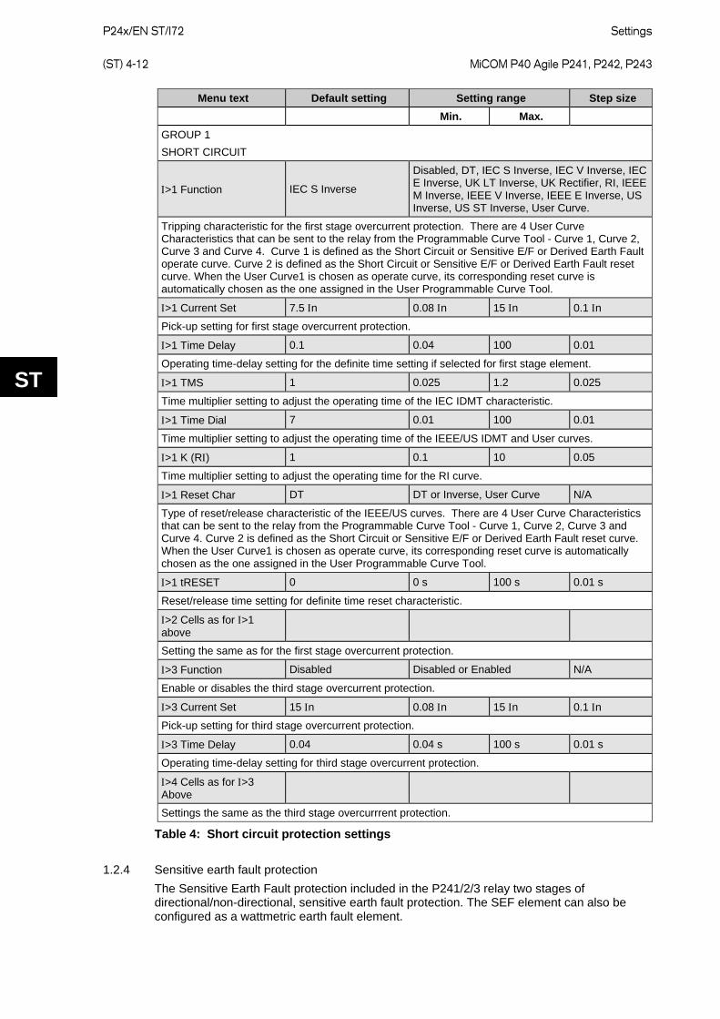
P24x/EN ST/I72
Settings (ST) 4-12 MiCOM P40 Agile P241, P242, P243
ST
Menu text Default setting Setting range Step size Min. Max.
GROUP 1 SHORT CIRCUIT
Ι>1 Function IEC S Inverse
Disabled, DT, IEC S Inverse, IEC V Inverse, IEC E Inverse, UK LT Inverse, UK Rectifier, RI, IEEE M Inverse, IEEE V Inverse, IEEE E Inverse, US Inverse, US ST Inverse, User Curve.
Tripping characteristic for the first stage overcurrent protection. There are 4 User Curve Characteristics that can be sent to the relay from the Programmable Curve Tool - Curve 1, Curve 2, Curve 3 and Curve 4. Curve 1 is defined as the Short Circuit or Sensitive E/F or Derived Earth Fault operate curve. Curve 2 is defined as the Short Circuit or Sensitive E/F or Derived Earth Fault reset curve. When the User Curve1 is chosen as operate curve, its corresponding reset curve is automatically chosen as the one assigned in the User Programmable Curve Tool.
Ι>1 Current Set 7.5 Ιn 0.08 Ιn 15 Ιn 0.1 Ιn
Pick-up setting for first stage overcurrent protection.
Ι>1 Time Delay 0.1 0.04 100 0.01
Operating time-delay setting for the definite time setting if selected for first stage element.
Ι>1 TMS 1 0.025 1.2 0.025
Time multiplier setting to adjust the operating time of the IEC IDMT characteristic.
Ι>1 Time Dial 7 0.01 100 0.01
Time multiplier setting to adjust the operating time of the IEEE/US IDMT and User curves.
Ι>1 K (RΙ) 1 0.1 10 0.05
Time multiplier setting to adjust the operating time for the RI curve.
Ι>1 Reset Char DT DT or Inverse, User Curve N/A
Type of reset/release characteristic of the IEEE/US curves. There are 4 User Curve Characteristics that can be sent to the relay from the Programmable Curve Tool - Curve 1, Curve 2, Curve 3 and Curve 4. Curve 2 is defined as the Short Circuit or Sensitive E/F or Derived Earth Fault reset curve. When the User Curve1 is chosen as operate curve, its corresponding reset curve is automatically chosen as the one assigned in the User Programmable Curve Tool.
Ι>1 tRESET 0 0 s 100 s 0.01 s
Reset/release time setting for definite time reset characteristic.
Ι>2 Cells as for Ι>1 above
Setting the same as for the first stage overcurrent protection.
Ι>3 Function Disabled Disabled or Enabled N/A
Enable or disables the third stage overcurrent protection.
Ι>3 Current Set 15 Ιn 0.08 Ιn 15 Ιn 0.1 Ιn
Pick-up setting for third stage overcurrent protection.
Ι>3 Time Delay 0.04 0.04 s 100 s 0.01 s
Operating time-delay setting for third stage overcurrent protection.
Ι>4 Cells as for Ι>3 Above
Settings the same as the third stage overcurrrent protection.
Table 4: Short circuit protection settings
1.2.4 Sensitive earth fault protection The Sensitive Earth Fault protection included in the P241/2/3 relay two stages of directional/non-directional, sensitive earth fault protection. The SEF element can also be configured as a wattmetric earth fault element.
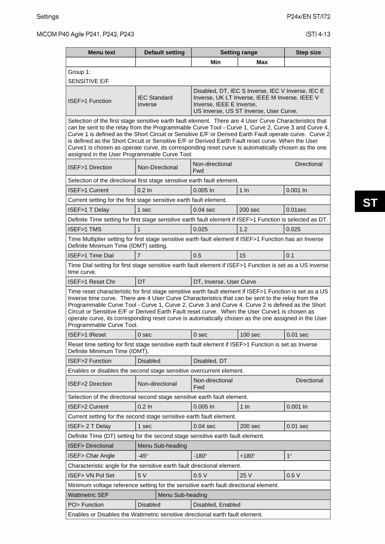
Settings
P24x/EN ST/I72 MiCOM P40 Agile P241, P242, P243 (ST) 4-13
ST
Menu text Default setting Setting range Step size Min Max
Group 1: SENSITIVE E/F
ISEF>1 Function IEC Standard Inverse
Disabled, DT, IEC S Inverse, IEC V Inverse, IEC E Inverse, UK LT Inverse, IEEE M Inverse, IEEE V Inverse, IEEE E Inverse, US Inverse, US ST Inverse, User Curve.
Selection of the first stage sensitive earth fault element. There are 4 User Curve Characteristics that can be sent to the relay from the Programmable Curve Tool - Curve 1, Curve 2, Curve 3 and Curve 4. Curve 1 is defined as the Short Circuit or Sensitive E/F or Derived Earth Fault operate curve. Curve 2 is defined as the Short Circuit or Sensitive E/F or Derived Earth Fault reset curve. When the User Curve1 is chosen as operate curve, its corresponding reset curve is automatically chosen as the one assigned in the User Programmable Curve Tool.
ISEF>1 Direction Non-Directional Non-directional Directional Fwd
Selection of the directional first stage sensitive earth fault element.
ISEF>1 Current 0.2 In 0.005 In 1 In 0.001 In
Current setting for the first stage sensitive earth fault element.
ISEF>1 T Delay 1 sec 0.04 sec 200 sec 0.01sec
Definite Time setting for first stage sensitive earth fault element if ISEF>1 Function is selected as DT.
ISEF>1 TMS 1 0.025 1.2 0.025
Time Multiplier setting for first stage sensitive earth fault element if ISEF>1 Function has an Inverse Definite Minimum Time (IDMT) setting.
ISEF>1 Time Dial 7 0.5 15 0.1
Time Dial setting for first stage sensitive earth fault element if ISEF>1 Function is set as a US inverse time curve.
ISEF>1 Reset Chr DT DT, Inverse, User Curve
Time reset characteristic for first stage sensitive earth fault element if ISEF>1 Function is set as a US Inverse time curve. There are 4 User Curve Characteristics that can be sent to the relay from the Programmable Curve Tool - Curve 1, Curve 2, Curve 3 and Curve 4. Curve 2 is defined as the Short Circuit or Sensitive E/F or Derived Earth Fault reset curve. When the User Curve1 is chosen as operate curve, its corresponding reset curve is automatically chosen as the one assigned in the User Programmable Curve Tool.
ISEF>1 tReset 0 sec 0 sec 100 sec 0.01 sec
Reset time setting for first stage sensitive earth fault element if ISEF>1 Function is set as Inverse Definite Minimum Time (IDMT).
ISEF>2 Function Disabled Disabled, DT
Enables or disables the second stage sensitive overcurrent element.
ISEF>2 Direction Non-directional Non-directional Directional Fwd
Selection of the directional second stage sensitive earth fault element.
ISEF>2 Current 0.2 In 0.005 In 1 In 0.001 In
Current setting for the second stage sensitive earth fault element.
ISEF> 2 T Delay 1 sec 0.04 sec 200 sec 0.01 sec
Definite Time (DT) setting for the second stage sensitive earth fault element.
ISEF> Directional Menu Sub-heading
ISEF> Char Angle -45° -180° +180° 1°
Characteristic angle for the sensitive earth fault directional element.
ISEF> VN Pol Set 5 V 0.5 V 25 V 0.5 V
Minimum voltage reference setting for the sensitive earth fault directional element.
Wattmetric SEF Menu Sub-heading
PO> Function Disabled Disabled, Enabled
Enables or Disables the Wattmetric sensitive directional earth fault element.
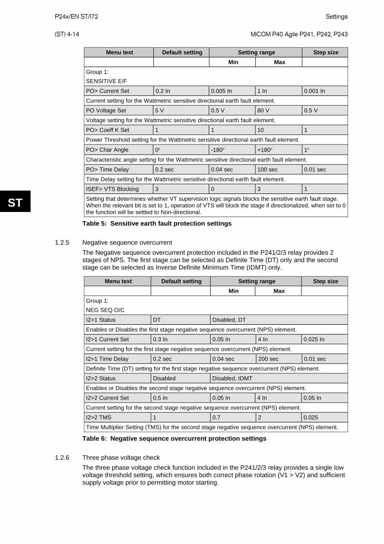
P24x/EN ST/I72
Settings (ST) 4-14 MiCOM P40 Agile P241, P242, P243
ST
Menu text Default setting Setting range Step size Min Max
Group 1: SENSITIVE E/F
PO> Current Set 0.2 In 0.005 In 1 In 0.001 In
Current setting for the Wattmetric sensitive directional earth fault element.
PO Voltage Set 5 V 0.5 V 80 V 0.5 V
Voltage setting for the Wattmetric sensitive directional earth fault element.
PO> Coeff K Set 1 1 10 1
Power Threshold setting for the Wattmetric sensitive directional earth fault element.
PO> Char Angle 0° -180° +180° 1°
Characteristic angle setting for the Wattmetric sensitive directional earth fault element.
PO> Time Delay 0.2 sec 0.04 sec 100 sec 0.01 sec
Time Delay setting for the Wattmetric sensitive directional earth fault element.
ISEF> VTS Blocking 3 0 3 1
Setting that determines whether VT supervision logic signals blocks the sensitive earth fault stage. When the relevant bit is set to 1, operation of VTS will block the stage if directionalized, when set to 0 the function will be settled to Non-directional.
Table 5: Sensitive earth fault protection settings
1.2.5 Negative sequence overcurrent The Negative sequence overcurrent protection included in the P241/2/3 relay provides 2 stages of NPS. The first stage can be selected as Definite Time (DT) only and the second stage can be selected as Inverse Definite Minimum Time (IDMT) only.
Menu text Default setting Setting range Step size Min Max
Group 1: NEG SEQ O/C
I2>1 Status DT Disabled, DT
Enables or Disables the first stage negative sequence overcurrent (NPS) element.
I2>1 Current Set 0.3 In 0.05 In 4 In 0.025 In
Current setting for the first stage negative sequence overcurrent (NPS) element.
I2>1 Time Delay 0.2 sec 0.04 sec 200 sec 0.01 sec
Definite Time (DT) setting for the first stage negative sequence overcurrent (NPS) element.
I2>2 Status Disabled Disabled, IDMT
Enables or Disables the second stage negative sequence overcurrent (NPS) element.
I2>2 Current Set 0.5 In 0.05 In 4 In 0.05 In
Current setting for the second stage negative sequence overcurrent (NPS) element.
I2>2 TMS 1 0.7 2 0.025
Time Multiplier Setting (TMS) for the second stage negative sequence overcurrent (NPS) element.
Table 6: Negative sequence overcurrent protection settings
1.2.6 Three phase voltage check The three phase voltage check function included in the P241/2/3 relay provides a single low voltage threshold setting, which ensures both correct phase rotation (V1 > V2) and sufficient supply voltage prior to permitting motor starting.
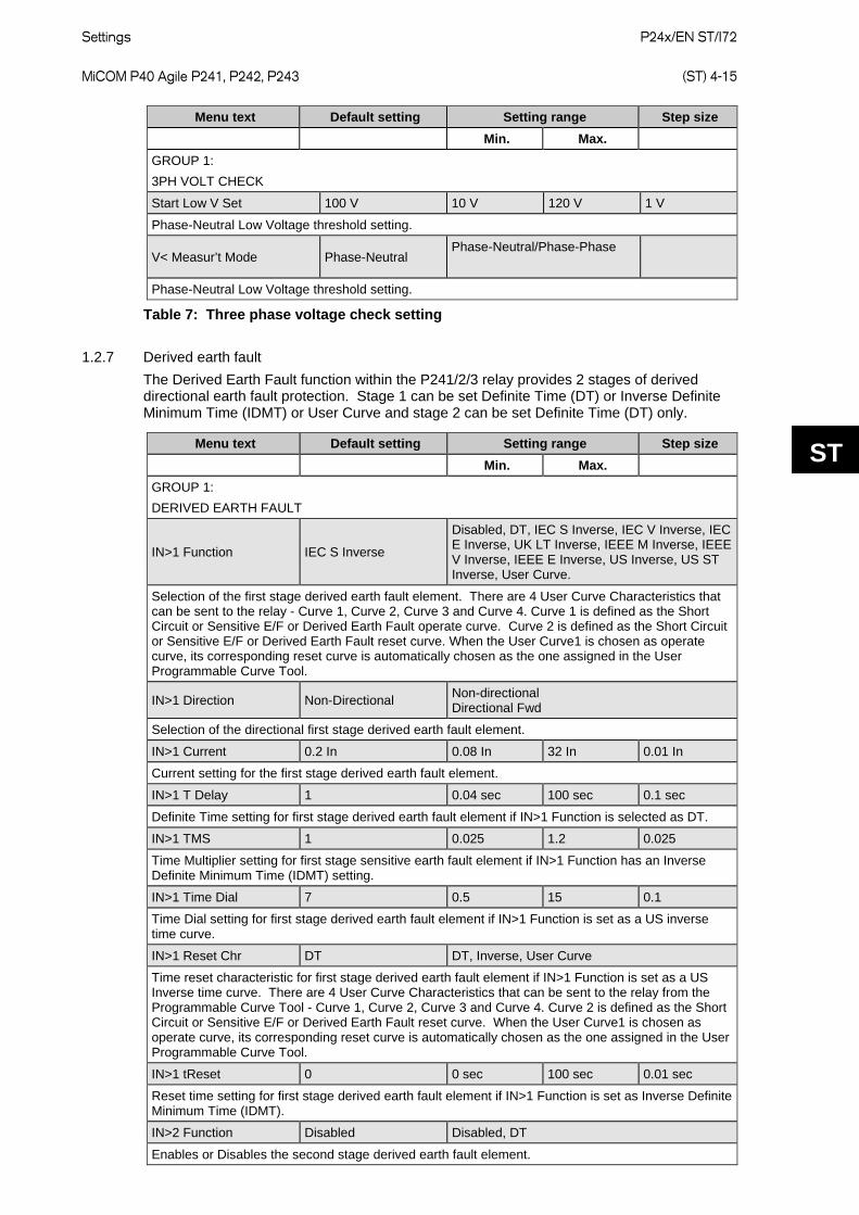
Settings
P24x/EN ST/I72 MiCOM P40 Agile P241, P242, P243 (ST) 4-15
ST
Menu text Default setting Setting range Step size Min. Max.
GROUP 1: 3PH VOLT CHECK
Start Low V Set 100 V 10 V 120 V 1 V
Phase-Neutral Low Voltage threshold setting.
V< Measur’t Mode Phase-Neutral Phase-Neutral/Phase-Phase
Phase-Neutral Low Voltage threshold setting.
Table 7: Three phase voltage check setting
1.2.7 Derived earth fault The Derived Earth Fault function within the P241/2/3 relay provides 2 stages of derived directional earth fault protection. Stage 1 can be set Definite Time (DT) or Inverse Definite Minimum Time (IDMT) or User Curve and stage 2 can be set Definite Time (DT) only.
Menu text Default setting Setting range Step size Min. Max.
GROUP 1: DERIVED EARTH FAULT
IN>1 Function IEC S Inverse
Disabled, DT, IEC S Inverse, IEC V Inverse, IEC E Inverse, UK LT Inverse, IEEE M Inverse, IEEE V Inverse, IEEE E Inverse, US Inverse, US ST Inverse, User Curve.
Selection of the first stage derived earth fault element. There are 4 User Curve Characteristics that can be sent to the relay - Curve 1, Curve 2, Curve 3 and Curve 4. Curve 1 is defined as the Short Circuit or Sensitive E/F or Derived Earth Fault operate curve. Curve 2 is defined as the Short Circuit or Sensitive E/F or Derived Earth Fault reset curve. When the User Curve1 is chosen as operate curve, its corresponding reset curve is automatically chosen as the one assigned in the User Programmable Curve Tool.
IN>1 Direction Non-Directional Non-directional Directional Fwd
Selection of the directional first stage derived earth fault element.
IN>1 Current 0.2 In 0.08 In 32 In 0.01 In
Current setting for the first stage derived earth fault element.
IN>1 T Delay 1 0.04 sec 100 sec 0.1 sec
Definite Time setting for first stage derived earth fault element if IN>1 Function is selected as DT.
IN>1 TMS 1 0.025 1.2 0.025
Time Multiplier setting for first stage sensitive earth fault element if IN>1 Function has an Inverse Definite Minimum Time (IDMT) setting.
IN>1 Time Dial 7 0.5 15 0.1
Time Dial setting for first stage derived earth fault element if IN>1 Function is set as a US inverse time curve.
IN>1 Reset Chr DT DT, Inverse, User Curve
Time reset characteristic for first stage derived earth fault element if IN>1 Function is set as a US Inverse time curve. There are 4 User Curve Characteristics that can be sent to the relay from the Programmable Curve Tool - Curve 1, Curve 2, Curve 3 and Curve 4. Curve 2 is defined as the Short Circuit or Sensitive E/F or Derived Earth Fault reset curve. When the User Curve1 is chosen as operate curve, its corresponding reset curve is automatically chosen as the one assigned in the User Programmable Curve Tool.
IN>1 tReset 0 0 sec 100 sec 0.01 sec
Reset time setting for first stage derived earth fault element if IN>1 Function is set as Inverse Definite Minimum Time (IDMT).
IN>2 Function Disabled Disabled, DT
Enables or Disables the second stage derived earth fault element.
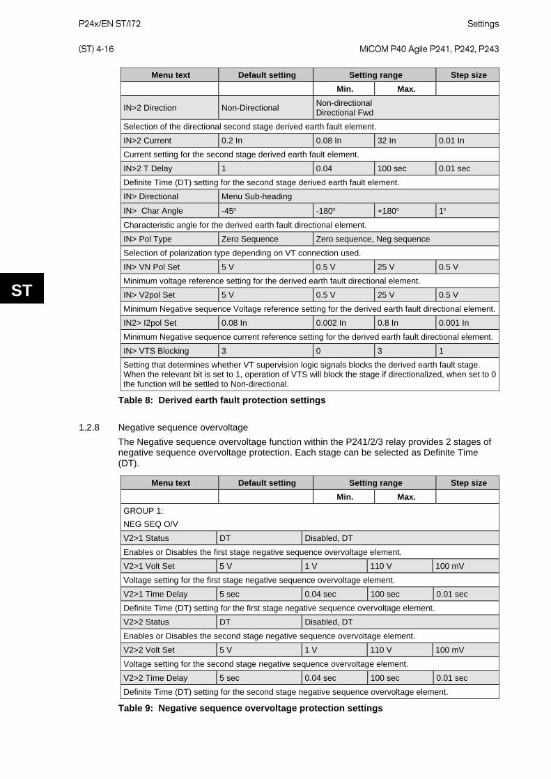
P24x/EN ST/I72
Settings (ST) 4-16 MiCOM P40 Agile P241, P242, P243
ST
Menu text Default setting Setting range Step size Min. Max.
IN>2 Direction Non-Directional Non-directional Directional Fwd
Selection of the directional second stage derived earth fault element.
IN>2 Current 0.2 In 0.08 In 32 In 0.01 In
Current setting for the second stage derived earth fault element.
IN>2 T Delay 1 0.04 100 sec 0.01 sec
Definite Time (DT) setting for the second stage derived earth fault element.
IN> Directional Menu Sub-heading
IN> Char Angle -45° -180° +180° 1°
Characteristic angle for the derived earth fault directional element.
IN> Pol Type Zero Sequence Zero sequence, Neg sequence
Selection of polarization type depending on VT connection used.
IN> VN Pol Set 5 V 0.5 V 25 V 0.5 V
Minimum voltage reference setting for the derived earth fault directional element.
IN> V2pol Set 5 V 0.5 V 25 V 0.5 V
Minimum Negative sequence Voltage reference setting for the derived earth fault directional element.
IN2> I2pol Set 0.08 In 0.002 In 0.8 In 0.001 In
Minimum Negative sequence current reference setting for the derived earth fault directional element.
IN> VTS Blocking 3 0 3 1
Setting that determines whether VT supervision logic signals blocks the derived earth fault stage. When the relevant bit is set to 1, operation of VTS will block the stage if directionalized, when set to 0 the function will be settled to Non-directional.
Table 8: Derived earth fault protection settings
1.2.8 Negative sequence overvoltage The Negative sequence overvoltage function within the P241/2/3 relay provides 2 stages of negative sequence overvoltage protection. Each stage can be selected as Definite Time (DT).
Menu text Default setting Setting range Step size Min. Max.
GROUP 1: NEG SEQ O/V
V2>1 Status DT Disabled, DT
Enables or Disables the first stage negative sequence overvoltage element.
V2>1 Volt Set 5 V 1 V 110 V 100 mV
Voltage setting for the first stage negative sequence overvoltage element.
V2>1 Time Delay 5 sec 0.04 sec 100 sec 0.01 sec
Definite Time (DT) setting for the first stage negative sequence overvoltage element.
V2>2 Status DT Disabled, DT
Enables or Disables the second stage negative sequence overvoltage element.
V2>2 Volt Set 5 V 1 V 110 V 100 mV
Voltage setting for the second stage negative sequence overvoltage element.
V2>2 Time Delay 5 sec 0.04 sec 100 sec 0.01 sec
Definite Time (DT) setting for the second stage negative sequence overvoltage element.
Table 9: Negative sequence overvoltage protection settings
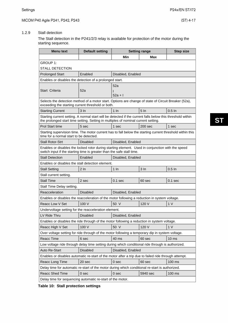
Settings
P24x/EN ST/I72 MiCOM P40 Agile P241, P242, P243 (ST) 4-17
ST
1.2.9 Stall detection The Stall detection in the P241/2/3 relay is available for protection of the motor during the starting sequence.
Menu text Default setting Setting range Step size Min Max
GROUP 1: STALL DETECTION
Prolonged Start Enabled Disabled, Enabled
Enables or disables the detection of a prolonged start.
Start Criteria 52a 52a I 52a + I
Selects the detection method of a motor start. Options are change of state of Circuit Breaker (52a), exceeding the starting current threshold or both.
Starting Current 3 In 1 In 5 In 0.5 In
Starting current setting. A normal start will be detected if the current falls below this threshold within the prolonged start time setting. Setting in multiples of nominal current setting.
Prol Start time 5 sec 1 sec 200 sec 1 sec
Starting supervision time. The motor current has to fall below the starting current threshold within this time for a normal start to be detected.
Stall Rotor-Strt Disabled Disabled, Enabled
Enables or disables the locked rotor during starting element. Used in conjunction with the speed switch input if the starting time is greater than the safe stall time.
Stall Detection Enabled Disabled, Enabled
Enables or disables the stall detection element.
Stall Setting 2 In 1 In 3 In 0.5 In
Stall current setting.
Stall Time 2 sec 0.1 sec 60 sec 0.1 sec
Stall Time Delay setting.
Reacceleration Disabled Disabled, Enabled
Enables or disables the reacceleration of the motor following a reduction in system voltage.
Reacc Low V Set 100 V 50 V 120 V 1 V
Undervoltage setting for the reacceleration element.
LV Ride Thru Disabled Disabled, Enabled
Enables or disables the ride through of the motor following a reduction in system voltage.
Reacc High V Set 100 V 50 V 120 V 1 V
Over voltage setting for ride through of the motor following a temporary dip in system voltage.
Reacc Time 6 sec 40 ms 60 sec 10 ms
Low voltage ride through delay time setting during which conditional ride through is authorized.
Auto Re-Start Disabled Disabled, Enabled
Enables or disables automatic re-start of the motor after a trip due to failed ride through attempt.
Reacc Long Time 20 sec 0 sec 60 sec 100 ms
Delay time for automatic re-start of the motor during which conditional re-start is authorized.
Reacc Shed Time 0 sec 0 sec 5940 sec 100 ms
Delay time for sequencing automatic re-start of the motor.
Table 10: Stall protection settings
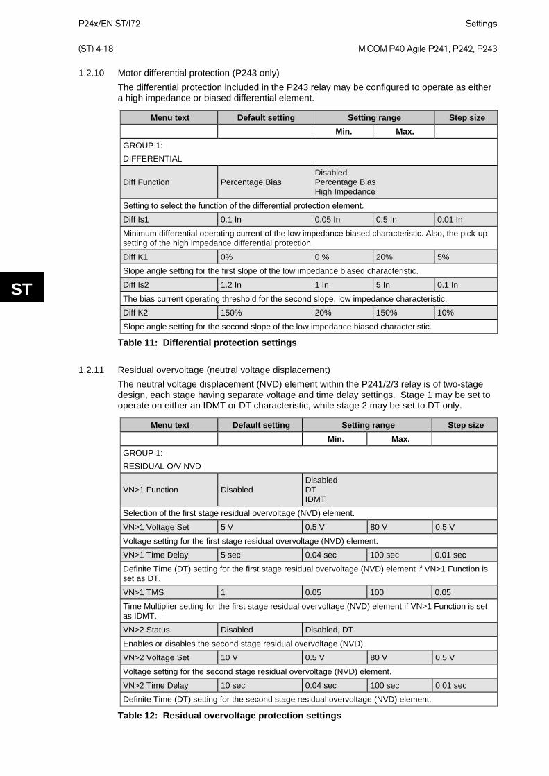
P24x/EN ST/I72
Settings (ST) 4-18 MiCOM P40 Agile P241, P242, P243
ST
1.2.10 Motor differential protection (P243 only) The differential protection included in the P243 relay may be configured to operate as either a high impedance or biased differential element.
Menu text Default setting Setting range Step size Min. Max.
GROUP 1: DIFFERENTIAL
Diff Function Percentage Bias Disabled Percentage Bias High Impedance
Setting to select the function of the differential protection element.
Diff Is1 0.1 In 0.05 In 0.5 In 0.01 In
Minimum differential operating current of the low impedance biased characteristic. Also, the pick-up setting of the high impedance differential protection.
Diff K1 0% 0 % 20% 5%
Slope angle setting for the first slope of the low impedance biased characteristic.
Diff Is2 1.2 In 1 In 5 In 0.1 In
The bias current operating threshold for the second slope, low impedance characteristic.
Diff K2 150% 20% 150% 10%
Slope angle setting for the second slope of the low impedance biased characteristic.
Table 11: Differential protection settings
1.2.11 Residual overvoltage (neutral voltage displacement) The neutral voltage displacement (NVD) element within the P241/2/3 relay is of two-stage design, each stage having separate voltage and time delay settings. Stage 1 may be set to operate on either an IDMT or DT characteristic, while stage 2 may be set to DT only.
Menu text Default setting Setting range Step size Min. Max.
GROUP 1: RESIDUAL O/V NVD
VN>1 Function Disabled Disabled DT IDMT
Selection of the first stage residual overvoltage (NVD) element.
VN>1 Voltage Set 5 V 0.5 V 80 V 0.5 V
Voltage setting for the first stage residual overvoltage (NVD) element.
VN>1 Time Delay 5 sec 0.04 sec 100 sec 0.01 sec
Definite Time (DT) setting for the first stage residual overvoltage (NVD) element if VN>1 Function is set as DT.
VN>1 TMS 1 0.05 100 0.05
Time Multiplier setting for the first stage residual overvoltage (NVD) element if VN>1 Function is set as IDMT.
VN>2 Status Disabled Disabled, DT
Enables or disables the second stage residual overvoltage (NVD).
VN>2 Voltage Set 10 V 0.5 V 80 V 0.5 V
Voltage setting for the second stage residual overvoltage (NVD) element.
VN>2 Time Delay 10 sec 0.04 sec 100 sec 0.01 sec
Definite Time (DT) setting for the second stage residual overvoltage (NVD) element.
Table 12: Residual overvoltage protection settings
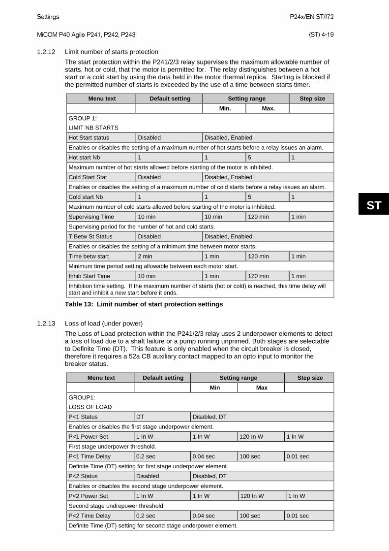
Settings
P24x/EN ST/I72 MiCOM P40 Agile P241, P242, P243 (ST) 4-19
ST
1.2.12 Limit number of starts protection The start protection within the P241/2/3 relay supervises the maximum allowable number of starts, hot or cold, that the motor is permitted for. The relay distinguishes between a hot start or a cold start by using the data held in the motor thermal replica. Starting is blocked if the permitted number of starts is exceeded by the use of a time between starts timer.
Menu text Default setting Setting range Step size Min. Max.
GROUP 1: LIMIT NB STARTS
Hot Start status Disabled Disabled, Enabled
Enables or disables the setting of a maximum number of hot starts before a relay issues an alarm.
Hot start Nb 1 1 5 1
Maximum number of hot starts allowed before starting of the motor is inhibited.
Cold Start Stat Disabled Disabled, Enabled
Enables or disables the setting of a maximum number of cold starts before a relay issues an alarm.
Cold start Nb 1 1 5 1
Maximum number of cold starts allowed before starting of the motor is inhibited.
Supervising Time 10 min 10 min 120 min 1 min
Supervising period for the number of hot and cold starts.
T Betw St Status Disabled Disabled, Enabled
Enables or disables the setting of a minimum time between motor starts.
Time betw start 2 min 1 min 120 min 1 min
Minimum time period setting allowable between each motor start.
Inhib Start Time 10 min 1 min 120 min 1 min
Inhibition time setting. If the maximum number of starts (hot or cold) is reached, this time delay will start and inhibit a new start before it ends.
Table 13: Limit number of start protection settings
1.2.13 Loss of load (under power) The Loss of Load protection within the P241/2/3 relay uses 2 underpower elements to detect a loss of load due to a shaft failure or a pump running unprimed. Both stages are selectable to Definite Time (DT). This feature is only enabled when the circuit breaker is closed, therefore it requires a 52a CB auxiliary contact mapped to an opto input to monitor the breaker status.
Menu text Default setting Setting range Step size Min Max
GROUP1: LOSS OF LOAD
P<1 Status DT Disabled, DT
Enables or disables the first stage underpower element.
P<1 Power Set 1 In W 1 In W 120 In W 1 In W
First stage underpower threshold.
P<1 Time Delay 0.2 sec 0.04 sec 100 sec 0.01 sec
Definite Time (DT) setting for first stage underpower element.
P<2 Status Disabled Disabled, DT
Enables or disables the second stage underpower element.
P<2 Power Set 1 In W 1 In W 120 In W 1 In W
Second stage undrepower threshold.
P<2 Time Delay 0.2 sec 0.04 sec 100 sec 0.01 sec
Definite Time (DT) setting for second stage underpower element.
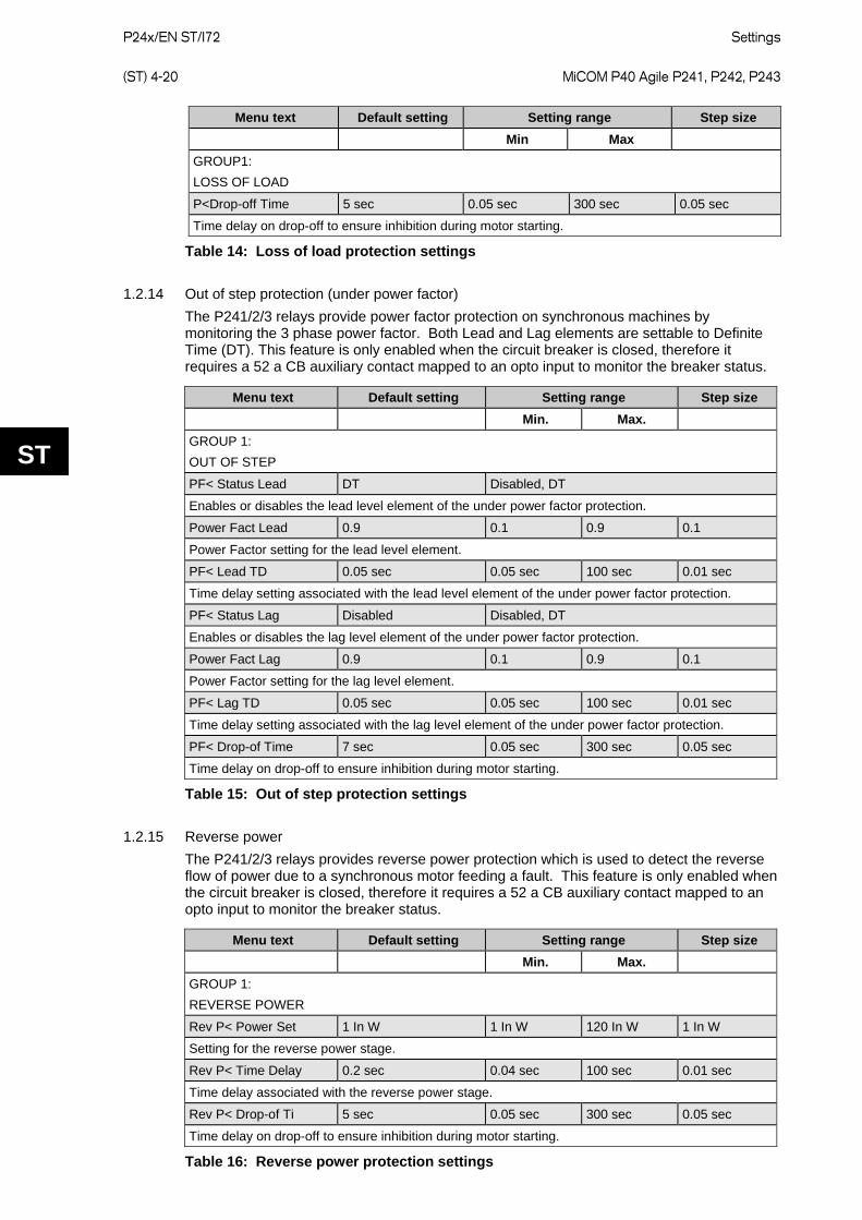
P24x/EN ST/I72
Settings (ST) 4-20 MiCOM P40 Agile P241, P242, P243
ST
Menu text Default setting Setting range Step size Min Max
GROUP1: LOSS OF LOAD
P<Drop-off Time 5 sec 0.05 sec 300 sec 0.05 sec
Time delay on drop-off to ensure inhibition during motor starting.
Table 14: Loss of load protection settings
1.2.14 Out of step protection (under power factor) The P241/2/3 relays provide power factor protection on synchronous machines by monitoring the 3 phase power factor. Both Lead and Lag elements are settable to Definite Time (DT). This feature is only enabled when the circuit breaker is closed, therefore it requires a 52 a CB auxiliary contact mapped to an opto input to monitor the breaker status.
Menu text Default setting Setting range Step size Min. Max.
GROUP 1: OUT OF STEP
PF< Status Lead DT Disabled, DT
Enables or disables the lead level element of the under power factor protection.
Power Fact Lead 0.9 0.1 0.9 0.1
Power Factor setting for the lead level element.
PF< Lead TD 0.05 sec 0.05 sec 100 sec 0.01 sec
Time delay setting associated with the lead level element of the under power factor protection.
PF< Status Lag Disabled Disabled, DT
Enables or disables the lag level element of the under power factor protection.
Power Fact Lag 0.9 0.1 0.9 0.1
Power Factor setting for the lag level element.
PF< Lag TD 0.05 sec 0.05 sec 100 sec 0.01 sec
Time delay setting associated with the lag level element of the under power factor protection.
PF< Drop-of Time 7 sec 0.05 sec 300 sec 0.05 sec
Time delay on drop-off to ensure inhibition during motor starting.
Table 15: Out of step protection settings
1.2.15 Reverse power The P241/2/3 relays provides reverse power protection which is used to detect the reverse flow of power due to a synchronous motor feeding a fault. This feature is only enabled when the circuit breaker is closed, therefore it requires a 52 a CB auxiliary contact mapped to an opto input to monitor the breaker status.
Menu text Default setting Setting range Step size Min. Max.
GROUP 1: REVERSE POWER
Rev P< Power Set 1 In W 1 In W 120 In W 1 In W
Setting for the reverse power stage.
Rev P< Time Delay 0.2 sec 0.04 sec 100 sec 0.01 sec
Time delay associated with the reverse power stage.
Rev P< Drop-of Ti 5 sec 0.05 sec 300 sec 0.05 sec
Time delay on drop-off to ensure inhibition during motor starting.
Table 16: Reverse power protection settings

Settings
P24x/EN ST/I72 MiCOM P40 Agile P241, P242, P243 (ST) 4-21
ST
1.2.16 Anti-Backspin protection The P241/2/3 relays provide anti-backspin protection.
Menu text Default setting Setting range Step size Min. Max.
GROUP 1: ANTI-BACKSPIN
VRem Antibacks 10 Vn 1 Vn 120 Vn 1 Vn
Setting of the remanent phase-phase voltage element.
Antibacks Delay 3000 secs 1 secs 7200 secs 1 secs
Time delay setting associated with the remanent voltage anti-backspin protection.
Table 17: Anti-Backspin protection settings
1.2.17 Field failure protection The field failure protection included in the P241/2/3 relay provides two impedance based stages of protection and a leading power factor alarm element.
Menu text Default setting Setting range Step size Min Max
GROUP1: FIELD FAILURE
FFail Alm Status Disabled Disabled, Enabled
Enables or disables the Field Failure Alarm function.
FFail Alm Angle -15° -75° 75° 1°
Pick-up setting for field failure alarm angle (leading power factor angle).
FFail Alm Delay 5 sec 0 sec 100 sec 0.1 sec
Operating time-delay setting of the field failure alarm.
FFail1 Status Enabled Disabled, Enabled
Enables or disables the first stage field failure protection function.
FFail1 Xal -20 /Ιn Ω -40/Ιn Ω 365/Ιn Ω 0.5/Ιn Ω
Negative reactance offset setting of first stage field failure impedance protection.
FFail1 Xb1 220/Ιn Ω 25/Ιn Ω 325/Ιn Ω 1/Ιn Ω
Diameter setting of circular impedance characteristic of first stage field failure protection.
FFail1 TimeDelay 5 sec 0 sec 100 sec 0.1 sec
Operating time-delay setting of the field failure first stage protection.
FFail1 DO Timer 0 s 0 s 10 s 0.1 s
Drop-off time-delay setting of the first stage field failure protection.
FFail2 Status Enabled Disabled, Enabled
Enables or disables the second stage field failure protection function.
FFail2 Xa2 -20/Ιn Ω -40/Ιn Ω 365/Ιn Ω 0.5/Ιn Ω
Negative reactance offset setting of second stage field failure impedance protection.
FFail2 Xb2 110/Ιn Ω 25/Ιn Ω 325/Ιn Ω 1/Ιn Ω
Diameter setting of circular impedance characteristic of second stage field failure protection.
FFail2 TimeDelay 0 s 0 s 100 s 0.1 s
Operating time-delay setting of the field failure second stage protection.
FFail2 DO Timer 0 s 0 s 10 s 0.1 s
Drop-off time-delay setting of the second stage field failure protection.
Table 18: Field failure protection settings

P24x/EN ST/I72
Settings (ST) 4-22 MiCOM P40 Agile P241, P242, P243
ST
1.2.18 Voltage protection The undervoltage and overvoltage protection included within the P241/2/3 relay both consist of two independent stages. The Undervoltage protection stage 1 can be set to Inverse Definite Minimum Time (IDMT) and the second stage can be set to Definite Time (DT). This feature is only enabled when the circuit breaker is closed, therefore it requires a 52a CB auxiliary contact mapped to an opto input to monitor the breaker status.
The overvoltage protection stage 1 and stage 2 can be set to Definite Time (DT) only.
Menu text Default setting Setting range Step size Min. Max.
GROUP 1: VOLT PROTECTION
UNDERVOLTAGE Menu Sub-heading
V< Measur’t Mode Phase-Phase Phase-Neutral, Phase-Phase
Sets the measured input voltage used for the undervoltage elements.
V< Operate Mode Any Phase Any Phase, Three Phase Determines whether any phase or all three phases must satisfy the undervoltage criteria before a decision is made.
V<1 Function Disabled Disabled DT IDMT
Selection of first stage undervoltage element.
V<1 Voltage Set 93 V 15 V 120 V 1 V
Setting of the first stage undervoltage element.
V<1 Time Delay 0.5 sec 0.04 sec 7200 sec 0.01 sec
Definite Time (DT) setting for the first stage undervoltage element if V<1 Function is set as DT.
V<1 TMS 1 0.5 100 0.01
Time Multiplier Setting of first stage undervoltage element if V<1 Function is set as IDMT.
V<2 Status Disabled Disabled/DT
.Selection of second stage undervoltage element.
V<2 Voltage Set 60 V 15 V 120 V 1 V
Setting of the second stage undervoltage element.
V<2 Time Delay 0.25 sec 0.04 sec 100 sec 0.01 sec
Definite Time (DT) setting for the first stage undervoltage element if V<1 Function is set as DT.
Inhib During St Disabled Disabled, Enabled
Setting to enable or disable the inhibit of undervoltage elements during motor starting.
GROUP 1: VOLT PROTECTION
OVERVOLTAGE Menu Sub-Heading
V> Measur’t Mode Phase-Phase Phase-Neutral, Phase-Phase
Sets the measured input voltage used for the overvoltage elements.
V> Operate Mode Any Phase Any Phase, Three Phase Determines whether any phase or all three phases must satisfy the overvoltage criteria before a decision is made. V>1 Status Disabled Disabled, DT
Enable or disables the first stage overvoltage element.
V>1 Voltage Set 165 V 50 V 200 V 1 V
Setting of the first stage overvoltage element.
V>1 Time Delay 10 sec 0.04 sec 7200 sec 0.01 sec
Definite Time (DT) setting for the first stage overvoltage element.
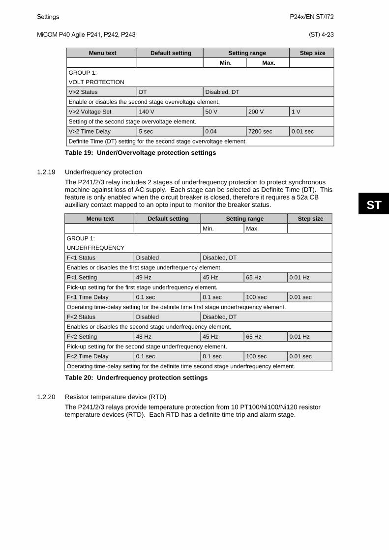
Settings
P24x/EN ST/I72 MiCOM P40 Agile P241, P242, P243 (ST) 4-23
ST
Menu text Default setting Setting range Step size Min. Max.
GROUP 1: VOLT PROTECTION
V>2 Status DT Disabled, DT
Enable or disables the second stage overvoltage element.
V>2 Voltage Set 140 V 50 V 200 V 1 V
Setting of the second stage overvoltage element.
V>2 Time Delay 5 sec 0.04 7200 sec 0.01 sec
Definite Time (DT) setting for the second stage overvoltage element.
Table 19: Under/Overvoltage protection settings
1.2.19 Underfrequency protection The P241/2/3 relay includes 2 stages of underfrequency protection to protect synchronous machine against loss of AC supply. Each stage can be selected as Definite Time (DT). This feature is only enabled when the circuit breaker is closed, therefore it requires a 52a CB auxiliary contact mapped to an opto input to monitor the breaker status.
Menu text Default setting Setting range Step size Min. Max.
GROUP 1: UNDERFREQUENCY
F<1 Status Disabled Disabled, DT
Enables or disables the first stage underfrequency element.
F<1 Setting 49 Hz 45 Hz 65 Hz 0.01 Hz
Pick-up setting for the first stage underfrequency element.
F<1 Time Delay 0.1 sec 0.1 sec 100 sec 0.01 sec
Operating time-delay setting for the definite time first stage underfrequency element.
F<2 Status Disabled Disabled, DT
Enables or disables the second stage underfrequency element.
F<2 Setting 48 Hz 45 Hz 65 Hz 0.01 Hz
Pick-up setting for the second stage underfrequency element.
F<2 Time Delay 0.1 sec 0.1 sec 100 sec 0.01 sec
Operating time-delay setting for the definite time second stage underfrequency element.
Table 20: Underfrequency protection settings
1.2.20 Resistor temperature device (RTD) The P241/2/3 relays provide temperature protection from 10 PT100/Ni100/Ni120 resistor temperature devices (RTD). Each RTD has a definite time trip and alarm stage.
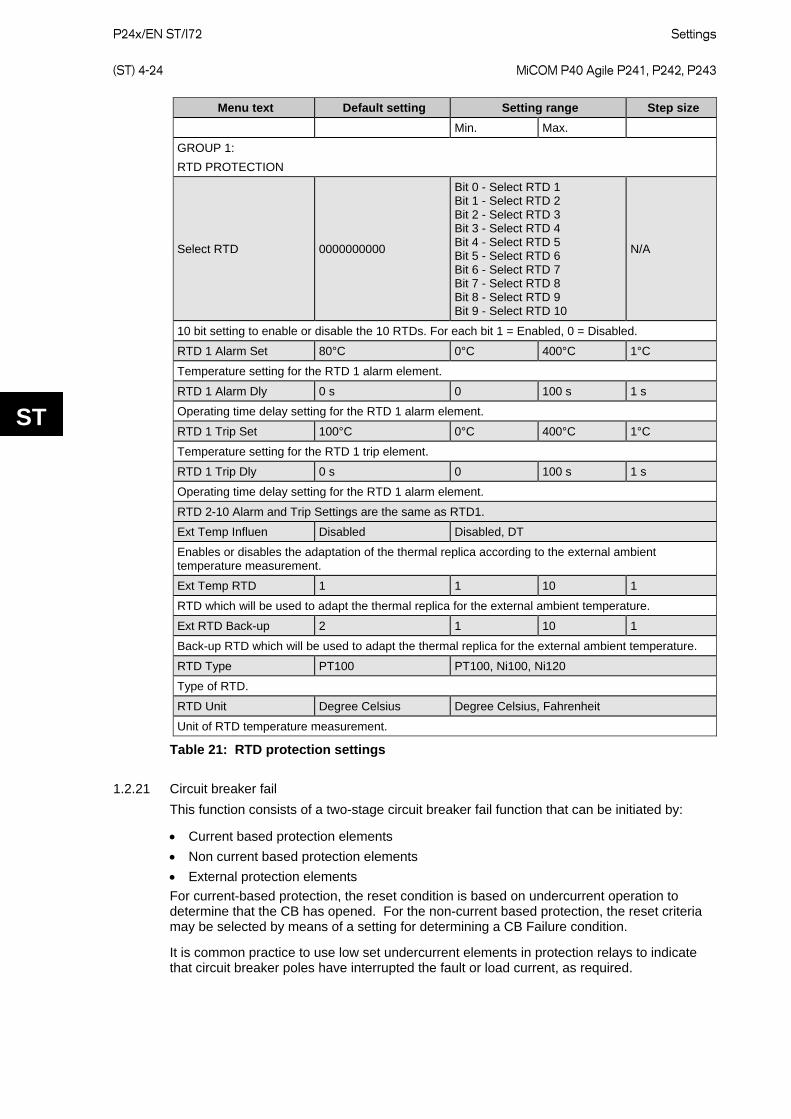
P24x/EN ST/I72
Settings (ST) 4-24 MiCOM P40 Agile P241, P242, P243
ST
Menu text Default setting Setting range Step size Min. Max.
GROUP 1: RTD PROTECTION
Select RTD 0000000000
Bit 0 - Select RTD 1 Bit 1 - Select RTD 2 Bit 2 - Select RTD 3 Bit 3 - Select RTD 4 Bit 4 - Select RTD 5 Bit 5 - Select RTD 6 Bit 6 - Select RTD 7 Bit 7 - Select RTD 8 Bit 8 - Select RTD 9 Bit 9 - Select RTD 10
N/A
10 bit setting to enable or disable the 10 RTDs. For each bit 1 = Enabled, 0 = Disabled.
RTD 1 Alarm Set 80°C 0°C 400°C 1°C
Temperature setting for the RTD 1 alarm element.
RTD 1 Alarm Dly 0 s 0 100 s 1 s
Operating time delay setting for the RTD 1 alarm element.
RTD 1 Trip Set 100°C 0°C 400°C 1°C
Temperature setting for the RTD 1 trip element.
RTD 1 Trip Dly 0 s 0 100 s 1 s
Operating time delay setting for the RTD 1 alarm element.
RTD 2-10 Alarm and Trip Settings are the same as RTD1.
Ext Temp Influen Disabled Disabled, DT
Enables or disables the adaptation of the thermal replica according to the external ambient temperature measurement.
Ext Temp RTD 1 1 10 1
RTD which will be used to adapt the thermal replica for the external ambient temperature.
Ext RTD Back-up 2 1 10 1
Back-up RTD which will be used to adapt the thermal replica for the external ambient temperature.
RTD Type PT100 PT100, Ni100, Ni120
Type of RTD.
RTD Unit Degree Celsius Degree Celsius, Fahrenheit
Unit of RTD temperature measurement.
Table 21: RTD protection settings
1.2.21 Circuit breaker fail This function consists of a two-stage circuit breaker fail function that can be initiated by:
• Current based protection elements • Non current based protection elements • External protection elements For current-based protection, the reset condition is based on undercurrent operation to determine that the CB has opened. For the non-current based protection, the reset criteria may be selected by means of a setting for determining a CB Failure condition.
It is common practice to use low set undercurrent elements in protection relays to indicate that circuit breaker poles have interrupted the fault or load current, as required.
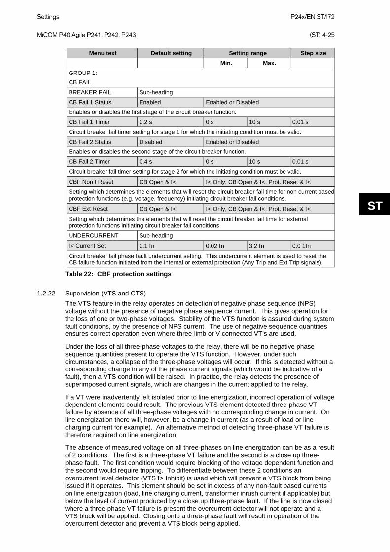
Settings
P24x/EN ST/I72 MiCOM P40 Agile P241, P242, P243 (ST) 4-25
ST
Menu text Default setting Setting range Step size Min. Max.
GROUP 1: CB FAIL
BREAKER FAIL Sub-heading
CB Fail 1 Status Enabled Enabled or Disabled
Enables or disables the first stage of the circuit breaker function.
CB Fail 1 Timer 0.2 s 0 s 10 s 0.01 s
Circuit breaker fail timer setting for stage 1 for which the initiating condition must be valid.
CB Fail 2 Status Disabled Enabled or Disabled
Enables or disables the second stage of the circuit breaker function.
CB Fail 2 Timer 0.4 s 0 s 10 s 0.01 s
Circuit breaker fail timer setting for stage 2 for which the initiating condition must be valid.
CBF Non I Reset CB Open & Ι< Ι< Only, CB Open & Ι<, Prot. Reset & Ι<
Setting which determines the elements that will reset the circuit breaker fail time for non current based protection functions (e.g. voltage, frequency) initiating circuit breaker fail conditions.
CBF Ext Reset CB Open & Ι< Ι< Only, CB Open & Ι<, Prot. Reset & Ι<
Setting which determines the elements that will reset the circuit breaker fail time for external protection functions initiating circuit breaker fail conditions.
UNDERCURRENT Sub-heading
I< Current Set 0.1 Ιn 0.02 Ιn 3.2 Ιn 0.0 1Ιn
Circuit breaker fail phase fault undercurrent setting. This undercurrent element is used to reset the CB failure function initiated from the internal or external protection (Any Trip and Ext Trip signals).
Table 22: CBF protection settings
1.2.22 Supervision (VTS and CTS) The VTS feature in the relay operates on detection of negative phase sequence (NPS) voltage without the presence of negative phase sequence current. This gives operation for the loss of one or two-phase voltages. Stability of the VTS function is assured during system fault conditions, by the presence of NPS current. The use of negative sequence quantities ensures correct operation even where three-limb or V connected VT’s are used.
Under the loss of all three-phase voltages to the relay, there will be no negative phase sequence quantities present to operate the VTS function. However, under such circumstances, a collapse of the three-phase voltages will occur. If this is detected without a corresponding change in any of the phase current signals (which would be indicative of a fault), then a VTS condition will be raised. In practice, the relay detects the presence of superimposed current signals, which are changes in the current applied to the relay.
If a VT were inadvertently left isolated prior to line energization, incorrect operation of voltage dependent elements could result. The previous VTS element detected three-phase VT failure by absence of all three-phase voltages with no corresponding change in current. On line energization there will, however, be a change in current (as a result of load or line charging current for example). An alternative method of detecting three-phase VT failure is therefore required on line energization.
The absence of measured voltage on all three-phases on line energization can be as a result of 2 conditions. The first is a three-phase VT failure and the second is a close up three-phase fault. The first condition would require blocking of the voltage dependent function and the second would require tripping. To differentiate between these 2 conditions an overcurrent level detector (VTS Ι> Inhibit) is used which will prevent a VTS block from being issued if it operates. This element should be set in excess of any non-fault based currents on line energization (load, line charging current, transformer inrush current if applicable) but below the level of current produced by a close up three-phase fault. If the line is now closed where a three-phase VT failure is present the overcurrent detector will not operate and a VTS block will be applied. Closing onto a three-phase fault will result in operation of the overcurrent detector and prevent a VTS block being applied.
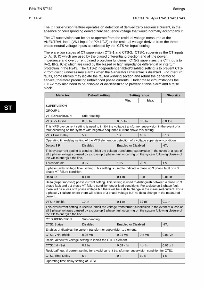
P24x/EN ST/I72
Settings (ST) 4-26 MiCOM P40 Agile P241, P242, P243
ST
The CT supervision feature operates on detection of derived zero sequence current, in the absence of corresponding derived zero sequence voltage that would normally accompany it.
The CT supervision can be set to operate from the residual voltage measured at the VNEUTRAL input (VN1 input for P241/2/3) or the residual voltage derived from the three phase-neutral voltage inputs as selected by the ‘CTS Vn Input’ setting.
There are two stages of CT supervision CTS-1 and CTS-2. CTS-1 supervises the CT inputs to IA, IB, IC which are used by the biased differential protection and all the power, impedance and overcurrent based protection functions. CTS-2 supervises the CT inputs to IA-2, IB-2, IC-2 which are used by the biased or high impedance differential or interturn protection in the P243. The CTS-2 independent enabled/disabled setting is to prevent CTS-2 from giving unnecessary alarms when the Generator Differential is disabled. For interturn faults, some utilities may isolate the faulted winding section and return the generator to service, therefore producing unbalanced phase currents. Under these circumstances the CTS-2 may also need to be disabled or de-sensitized to prevent a false alarm and a false block.
Menu text Default setting Setting range Step size Min. Max.
SUPERVISION GROUP 1
VT SUPERVISION Sub-heading
VTS Ι2> Inhibit 0.05 Ιn 0.05 Ιn 0.5 Ιn 0.0 1Ιn
This NPS overcurrent setting is used to inhibit the voltage transformer supervision in the event of a fault occurring on the system with negative sequence current above this setting.
VTS Time Delay 5 s 1 s 10 s 0.1 s
Operating time-delay setting of the VTS element on detection of a voltage supervision condition.
Detect 3 P Disabled Enabled or Disabled N/A
This overcurrent setting is used to inhibit the voltage transformer supervision in the event of a loss of all 3 phase voltages caused by a close up 3 phase fault occurring on the system following closure of the CB to energize the line.
Threshold 3P 30 V 10 V 70 V 1 V
3 phase under voltage level setting. This setting is used to indicate a close up 3 phase fault or a 3 phase VT failure condition.
Delta I > 0.1 In 0.1 In 5 In 0.01 In
Delta (superimposed) phase current setting. This setting is used to distinguish between a close up 3 phase fault and a 3 phase VT failure condition under load conditions. For a close up 3 phase fault there will be a loss of 3 phase voltage but there will be a delta change in the measured current. For a 3 phase VT failure where there will a loss of 3 phase voltage but no delta change in the measured current.
VTS Ι> Inhibit 10 Ιn 0.1 Ιn 32 Ιn 0.1 Ιn
This overcurrent setting is used to inhibit the voltage transformer supervision in the event of a loss of all 3 phase voltages caused by a close up 3 phase fault occurring on the system following closure of the CB to energize the line.
CT SUPERVISION Sub-heading
CTS1 Status Disabled Enabled or Disabled N/A
Enables or disables the current transformer supervision 1 element.
CTS1 VN< Inhibit 0.05 Vn 0.01 Vn 0.2 Vn 0.01 Vn
Residual/neutral voltage setting to inhibit the CTS1 element.
CTS1 ΙN> Set 0.2 Ιn 0.08 x Ιn 4 x Ιn 0.01 x Ιn
Residual/neutral current setting for a valid current transformer supervision condition for CTS1.
CTS1 Time Delay 5 s 0 s 10 s 1 s
Operating time-delay setting of CTS1.
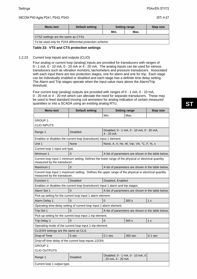
Settings
P24x/EN ST/I72 MiCOM P40 Agile P241, P242, P243 (ST) 4-27
ST
Menu text Default setting Setting range Step size Min. Max.
CTS2 settings are the same as CTS1
To be used only for P243 differential protection scheme.
Table 23: VTS and CTS protection settings
1.2.23 Current loop inputs and outputs (CLIO) Four analog or current loop (analog) inputs are provided for transducers with ranges of 0 - 1 mA, 0 - 10 mA, 0 - 20 mA or 4 - 20 mA. The analog inputs can be used for various transducers such as vibration monitors, tachometers and pressure transducers. Associated with each input there are two protection stages, one for alarm and one for trip. Each stage can be individually enabled or disabled and each stage has a definite time delay setting. The Alarm and Trip stages operate when the input value rises above the Alarm/Trip threshold.
Four current loop (analog) outputs are provided with ranges of 0 - 1 mA, 0 - 10 mA, 0 - 20 mA or 4 - 20 mA which can alleviate the need for separate transducers. These may be used to feed standard moving coil ammeters for analog indication of certain measured quantities or into a SCADA using an existing analog RTU.
Menu text Default setting Setting range Step size Min. Max.
GROUP 1: CLIO INPUTS
Range 1 Disabled Disabled, 0 - 1 mA, 0 - 10 mA, 0 - 20 mA, 4 - 20 mA
Enables or disables the current loop (transducer) input 1 element.
Unit 1 None None, A, V, Hz, W, Var, VA, °C, F, %, s
Current loop 1 input unit type.
Minimum 1 0 A list of parameters are shown in the table below.
Current loop input 1 minimum setting. Defines the lower range of the physical or electrical quantity measured by the transducer.
Maximum 1 0 A list of parameters are shown in the table below.
Current loop input 1 maximum setting. Defines the upper range of the physical or electrical quantity measured by the transducer.
Function 1 Disabled Disabled, Enabled
Enables or disables the current loop (transducer) input 1 alarm and trip stages.
Alarm Set 1 0 A list of parameters are shown in the table below.
Pick-up setting for the current loop input 1 alarm element.
Alarm Delay 1 0 0 300 s 1 s
Operating time-delay setting of current loop input 1 alarm element.
Trip Set 1 0 A list of parameters are shown in the table below.
Pick-up setting for the current loop input 1 trip element.
Trip Delay 1 0 0 300 s 1 s
Operating mode of the current loop input 1 trip element.
CLI2/3/4 settings are the same as CLI1
Drop-of Time 5 sec 0.1 sec 300 sec 0.1 sec
Drop-off time delay of the current loop inputs 1/2/3/4.
GROUP 1: CLIO OUTPUTS
Range 1 Disabled Disabled, 0 - 1 mA, 0 - 10 mA, 0 - 20 mA, 4 - 20 mA
Current loop 1 output type.
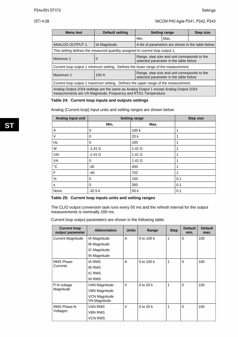
P24x/EN ST/I72
Settings (ST) 4-28 MiCOM P40 Agile P241, P242, P243
ST
Menu text Default setting Setting range Step size Min. Max.
ANALOG OUTPUT 1 IA Magnitude A list of parameters are shown in the table below
This setting defines the measured quantity assigned to current loop output 1.
Minimum 1 0 Range, step size and unit corresponds to the selected parameter in the table below
Current loop output 1 minimum setting. Defines the lower range of the measurement.
Maximum 1 100 A Range, step size and unit corresponds to the selected parameter in the table below
Current loop output 1 maximum setting. Defines the upper range of the measurement.
Analog Output 2/3/4 settings are the same as Analog Output 1 except Analog Output 2/3/4 measurements are VA Magnitude, Frequency and RTD1 Temperature.
Table 24: Current loop inputs and outputs settings
Analog (Current loop) input units and setting ranges are shown below
Analog input unit Setting range Step size Min. Max.
A 0 100 k 1
V 0 20 k 1
Hz 0 100 1
W -1.41 G 1.41 G 1
VAr -1.41 G 1.41 G 1
VA 0 1.41 G 1
°C -40 400 1
F -40 752 1
% 0 150 0.1
s 0 300 0.1
None -32.5 k 50 k 0.1
Table 25: Current loop inputs units and setting ranges
The CLIO output conversion task runs every 50 ms and the refresh interval for the output measurements is nominally 200 ms.
Current loop output parameters are shown in the following table:
Current loop output parameter Abbreviation Units Range Step Default
min. Default max.
Current Magnitude IA Magnitude IB Magnitude IC Magnitude IN Magnitude
A 0 to 100 k 1 0 100
RMS Phase Currents
IA RMS IB RMS IC RMS IN RMS
A 0 to 100 k 1 0 100
P-N voltage Magnitude
VAN Magnitude VBN Magnitude VCN Magnitude VN Magnitude
V 0 to 20 k 1 0 100
RMS Phase-N Voltages
VAN RMS VBN RMS VCN RMS
V 0 to 20 k 1 0 100
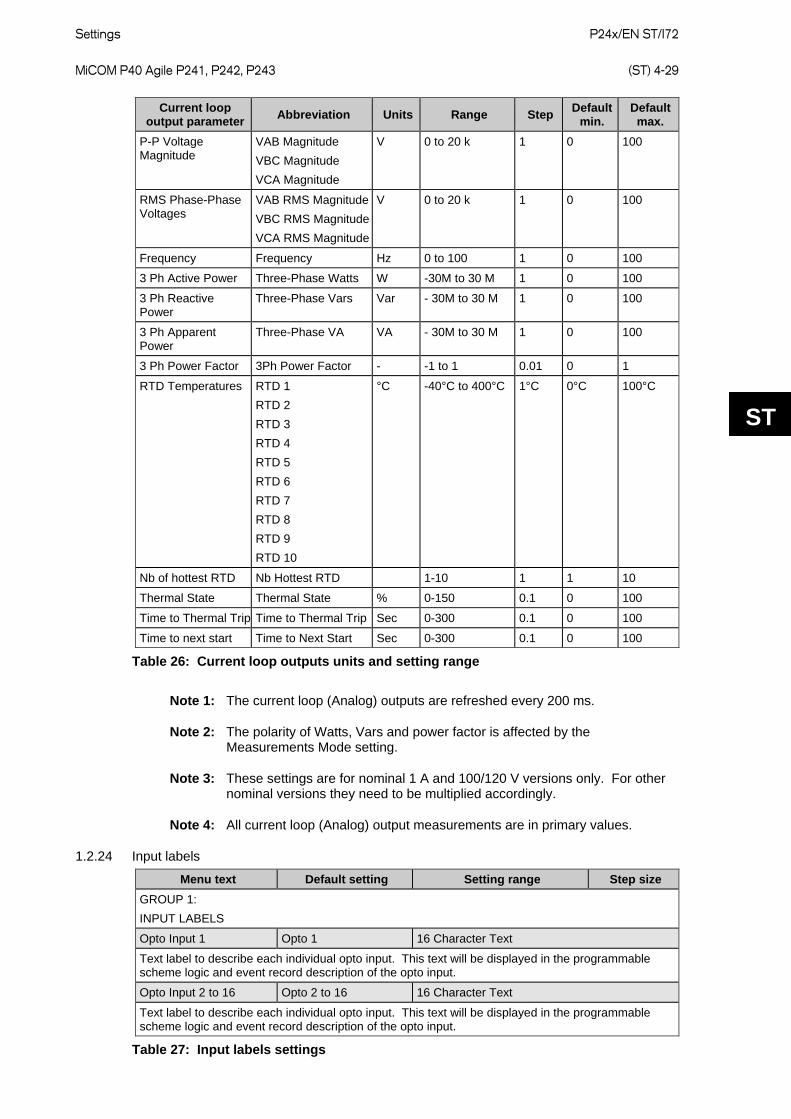
Settings
P24x/EN ST/I72 MiCOM P40 Agile P241, P242, P243 (ST) 4-29
ST
Current loop output parameter Abbreviation Units Range Step Default
min. Default max.
P-P Voltage Magnitude
VAB Magnitude VBC Magnitude VCA Magnitude
V 0 to 20 k 1 0 100
RMS Phase-Phase Voltages
VAB RMS Magnitude VBC RMS Magnitude VCA RMS Magnitude
V 0 to 20 k 1 0 100
Frequency Frequency Hz 0 to 100 1 0 100
3 Ph Active Power Three-Phase Watts W -30M to 30 M 1 0 100
3 Ph Reactive Power
Three-Phase Vars Var - 30M to 30 M 1 0 100
3 Ph Apparent Power
Three-Phase VA VA - 30M to 30 M 1 0 100
3 Ph Power Factor 3Ph Power Factor - -1 to 1 0.01 0 1
RTD Temperatures RTD 1 RTD 2 RTD 3 RTD 4 RTD 5 RTD 6 RTD 7 RTD 8 RTD 9 RTD 10
°C -40°C to 400°C 1°C 0°C 100°C
Nb of hottest RTD Nb Hottest RTD 1-10 1 1 10
Thermal State Thermal State % 0-150 0.1 0 100
Time to Thermal Trip Time to Thermal Trip Sec 0-300 0.1 0 100
Time to next start Time to Next Start Sec 0-300 0.1 0 100
Table 26: Current loop outputs units and setting range
Note 1: The current loop (Analog) outputs are refreshed every 200 ms.
Note 2: The polarity of Watts, Vars and power factor is affected by the Measurements Mode setting.
Note 3: These settings are for nominal 1 A and 100/120 V versions only. For other nominal versions they need to be multiplied accordingly.
Note 4: All current loop (Analog) output measurements are in primary values.
1.2.24 Input labels
Menu text Default setting Setting range Step size GROUP 1: INPUT LABELS
Opto Input 1 Opto 1 16 Character Text
Text label to describe each individual opto input. This text will be displayed in the programmable scheme logic and event record description of the opto input.
Opto Input 2 to 16 Opto 2 to 16 16 Character Text
Text label to describe each individual opto input. This text will be displayed in the programmable scheme logic and event record description of the opto input.
Table 27: Input labels settings

P24x/EN ST/I72
Settings (ST) 4-30 MiCOM P40 Agile P241, P242, P243
ST
1.2.25 Output labels
Menu text Default setting Setting range Step size GROUP 1: OUTPUT LABELS
Relay 1 Relay 1 16 Character Text
Text label to describe each individual relay output contact. This text will be displayed in the programmable scheme logic and event record description of the relay output contact.
Relay 2 to 16 Relay 2 to Relay 16 16 Character Text
Text label to describe each individual relay output contact. This text will be displayed in the programmable scheme logic and event record description of the relay output contact.
Table 28: Output labels settings
1.2.26 RTD labels
Menu text Default setting Setting range Step size GROUP 1: RTD LABELS
RTD 1 RTD 1 16 Character Text
Text label to describe each individual RTD. This text will be displayed in the Measurements 3 menu and fault records for the description of the RTDs.
RTD 2 to 10 RTD 2 to RTD 10 16 Character Text
Text label to describe each individual RTD. This text will be displayed in the Measurements 3 menu and fault records for the description of the RTDs.
Table 29: RTD labels settings
1.2.27 Analog Input labels
Menu text Default setting Setting range Step size GROUP 1: CLIO LABELS
CLIO Input 1 Analog Input 1 16 Character Text
Text label to describe each individual current loop/analogue input. This text will be displayed in the Measurements 3 menu and fault records for the description of the current loop/analogue inputs.
CLIO Input 2 to 4 Analog Input 2 to 4 16 Character Text
Text label to describe each individual current loop/analogue input. This text will be displayed in the Measurements 3 menu and fault records for the description of the current loop/analogue inputs.
Table 30: Current loop analog input label settings
1.3 Control and support settings The control and support settings are part of the main menu and are used to configure the relays global configuration. It includes submenu settings as below which are discussed in more detail below:
• Relay function configuration settings • Open/close circuit breaker • CT & VT ratio settings • Reset LEDs • Active protection setting group • Password & language settings • Circuit breaker control & monitoring settings • Communications settings • Measurement settings • Event & fault record settings

Settings
P24x/EN ST/I72 MiCOM P40 Agile P241, P242, P243 (ST) 4-31
ST
• User interface settings • Commissioning settings
1.3.1 System data This menu provides information for the device and general status of the relay.
Menu text Default setting Setting range Step size Min. Max.
SYSTEM DATA
Language English English, Francais, Deutsch, Espanol, Chinese & Russian N/A
The default language used by the device. Selectable as English, French, German, Spanish.
Password ****
Device password for level 1 or 2. If password level 1 is input then the access level is set as 1 and if password level 2 is input then the access level is set as 2.
Description MiCOM
16 character relay description. Can be edited.
Plant Reference MiCOM
Plant description. Can be edited.
Model Number P241??????0600J P242??????0600K P243??????0600K
Relay model number.
Serial Number 149188B
Relay serial number.
Frequency 50 Hz 50 Hz 60 Hz 10 Hz
Relay set frequency. Settable as 50 or 60 Hz.
Comms. Level
Displays the conformance of the relay to the Courier Level 2 comms.
Relay Address
Sets the first rear port relay address.
Plant Status 0000000000000000
Displays the circuit breaker plant status for up to 8 circuit breakers. The P24x relay supports only a single circuit breaker configuration.
Control Status 0000000000000000
Not used.
Active Group 1
Displays the active settings group.
CB Trip/Close No Operation No Operation, Trip, Close
Manually trips/closes the relay.
Software Ref. 1
Displays the relay software version including protocol and relay model. Software Ref.
Opto I/P Status 0000000000000000
This menu cell displays the status of the relay’s opto-isolated inputs as a binary string, a 1 indicating an energized opto-isolated input and a 0 a de-energized one.
Relay O/P Status 0000001000000000
This menu cell displays the status of the relay’s output contacts as a binary string, a 1 indicating an operated state and 0 a non-operated state.
Alarm Status 1 00000000000000000000000000000000
This menu cell displays the status of the first 32 alarms as a binary string, a 1 indicating an ON state and 0 an OFF state. Includes fixed and user settable alarms. See Data Type G96 in the Relay Menu Database for more details.
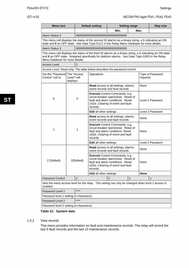
P24x/EN ST/I72
Settings (ST) 4-32 MiCOM P40 Agile P241, P242, P243
ST
Menu text Default setting Setting range Step size Min. Max.
Alarm Status 2 00000000000000000000000000000000
This menu cell displays the status of the second 32 alarms as a binary string, a 1 indicating an ON state and 0 an OFF state. See Data Type G111 in the Relay Menu Database for more details.
Alarm Status 3 00000000000000000000000000000000
This menu cell displays the status of the third 32 alarms as a binary string, a 1 indicating an ON state and 0 an OFF state. Assigned specifically for platform alarms. See Data Type G303 in the Relay Menu Database for more details.
Access Level 2
Access Level. Read only. The table below describes the password control.
Set the "Password Control" cell to
The "Access Level" cell displays
Operations Type of Password required
0 0
Read access to all settings, alarms, event records and fault records
None
Execute Control Commands, e.g. circuit breaker open/close. Reset of fault and alarm conditions. Reset LEDs. Clearing of event and fault records.
Level 1 Password
Edit all other settings Level 2 Password
1 1
Read access to all settings, alarms, event records and fault records None
Execute Control Commands, e.g. circuit breaker open/close. Reset of fault and alarm conditions. Reset LEDs. Clearing of event and fault records.
None
Edit all other settings Level 2 Password
2 (Default) 2(Default)
Read access to all settings, alarms, event records and fault records None
Execute Control Commands, e.g. circuit breaker open/close. Reset of fault and alarm conditions. Reset LEDs. Clearing of event and fault records.
None
Edit all other settings None Password Control 2 0 2 1
Sets the menu access level for the relay. This setting can only be changed when level 2 access is enabled.
Password Level 1 ****
Password level 1 setting (4 characters).
Password Level 2 ****
Password level 2 setting (4 characters).
Table 31: System data
1.3.2 View records This menu provides information on fault and maintenance records. The relay will record the last 5 fault records and the last 10 maintenance records.
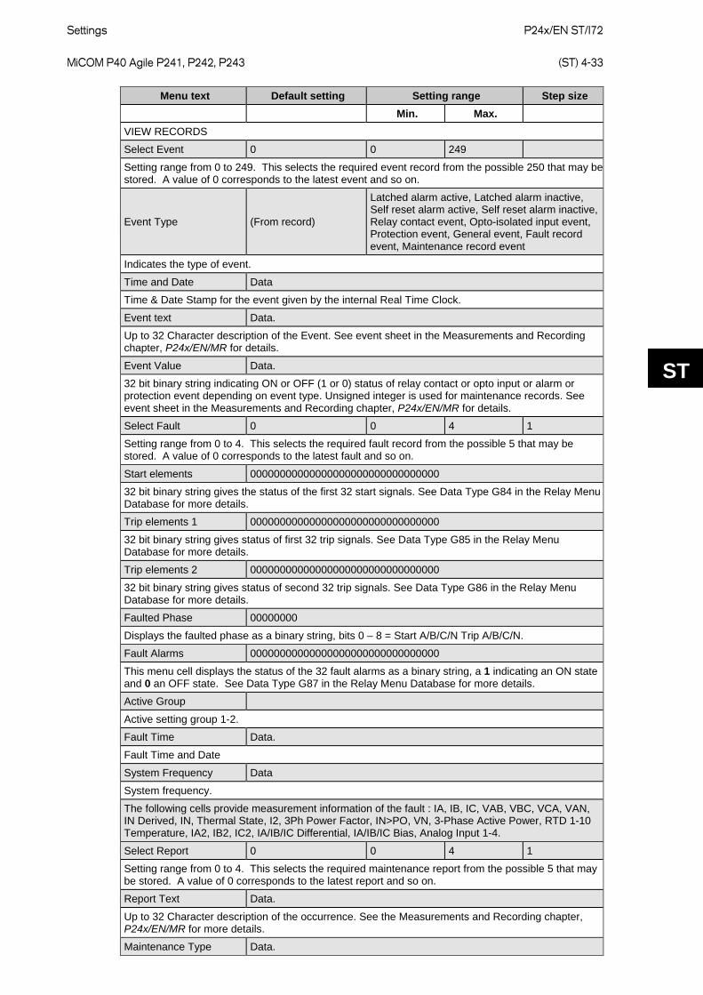
Settings
P24x/EN ST/I72 MiCOM P40 Agile P241, P242, P243 (ST) 4-33
ST
Menu text Default setting Setting range Step size Min. Max.
VIEW RECORDS
Select Event 0 0 249
Setting range from 0 to 249. This selects the required event record from the possible 250 that may be stored. A value of 0 corresponds to the latest event and so on.
Event Type (From record)
Latched alarm active, Latched alarm inactive, Self reset alarm active, Self reset alarm inactive, Relay contact event, Opto-isolated input event, Protection event, General event, Fault record event, Maintenance record event
Indicates the type of event.
Time and Date Data
Time & Date Stamp for the event given by the internal Real Time Clock.
Event text Data.
Up to 32 Character description of the Event. See event sheet in the Measurements and Recording chapter, P24x/EN/MR for details.
Event Value Data.
32 bit binary string indicating ON or OFF (1 or 0) status of relay contact or opto input or alarm or protection event depending on event type. Unsigned integer is used for maintenance records. See event sheet in the Measurements and Recording chapter, P24x/EN/MR for details.
Select Fault 0 0 4 1
Setting range from 0 to 4. This selects the required fault record from the possible 5 that may be stored. A value of 0 corresponds to the latest fault and so on.
Start elements 00000000000000000000000000000000
32 bit binary string gives the status of the first 32 start signals. See Data Type G84 in the Relay Menu Database for more details.
Trip elements 1 00000000000000000000000000000000
32 bit binary string gives status of first 32 trip signals. See Data Type G85 in the Relay Menu Database for more details.
Trip elements 2 00000000000000000000000000000000
32 bit binary string gives status of second 32 trip signals. See Data Type G86 in the Relay Menu Database for more details.
Faulted Phase 00000000
Displays the faulted phase as a binary string, bits 0 – 8 = Start A/B/C/N Trip A/B/C/N.
Fault Alarms 00000000000000000000000000000000
This menu cell displays the status of the 32 fault alarms as a binary string, a 1 indicating an ON state and 0 an OFF state. See Data Type G87 in the Relay Menu Database for more details.
Active Group
Active setting group 1-2.
Fault Time Data.
Fault Time and Date
System Frequency Data
System frequency.
The following cells provide measurement information of the fault : IA, IB, IC, VAB, VBC, VCA, VAN, IN Derived, IN, Thermal State, I2, 3Ph Power Factor, IN>PO, VN, 3-Phase Active Power, RTD 1-10 Temperature, IA2, IB2, IC2, IA/IB/IC Differential, IA/IB/IC Bias, Analog Input 1-4.
Select Report 0 0 4 1
Setting range from 0 to 4. This selects the required maintenance report from the possible 5 that may be stored. A value of 0 corresponds to the latest report and so on.
Report Text Data.
Up to 32 Character description of the occurrence. See the Measurements and Recording chapter, P24x/EN/MR for more details.
Maintenance Type Data.
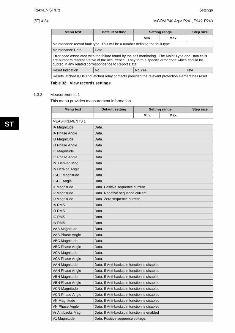
P24x/EN ST/I72
Settings (ST) 4-34 MiCOM P40 Agile P241, P242, P243
ST
Menu text Default setting Setting range Step size Min. Max.
Maintenance record fault type. This will be a number defining the fault type.
Maintenance Data Data.
Error code associated with the failure found by the self monitoring. The Maint Type and Data cells are numbers representative of the occurrence. They form a specific error code which should be quoted in any related correspondence to Report Data.
Reset Indication No No/Yes N/A
Resets latched lEDs and latched relay contacts provided the relevant protection element has reset.
Table 32: View records settings
1.3.3 Measurements 1 This menu provides measurement information.
Menu text Default setting Setting range Step size Min. Max.
MEASUREMENTS 1
IA Magnitude Data.
IA Phase Angle Data.
IB Magnitude Data.
IB Phase Angle Data
IC Magnitude Data.
IC Phase Angle Data.
IN Derived Mag Data.
IN Derived Angle Data.
I SEF Magnitude Data.
I SEF Angle Data.
I1 Magnitude Data. Positive sequence current.
I2 Magnitude Data. Negative sequence current.
I0 Magnitude Data. Zero sequence current.
IA RMS Data.
IB RMS Data.
IC RMS Data.
IN RMS Data
VAB Magnitude Data.
VAB Phase Angle Data.
VBC Magnitude Data.
VBC Phase Angle Data.
VCA Magnitude Data.
VCA Phase Angle Data.
VAN Magnitude Data. If Anti-backspin function is disabled
VAN Phase Angle Data. If Anti-backspin function is disabled
VBN Magnitude Data. If Anti-backspin function is disabled
VBN Phase Angle Data. If Anti-backspin function is disabled
VCN Magnitude Data. If Anti-backspin function is disabled
VCN Phase Angle Data. If Anti-backspin function is disabled
VN Magnitude Data. If Anti-backspin function is disabled
VN Phase Angle Data. If Anti-backspin function is disabled
Vr Antibacks Mag Data. If Anti-backspin function is enabled
V1 Magnitude Data. Positive sequence voltage.
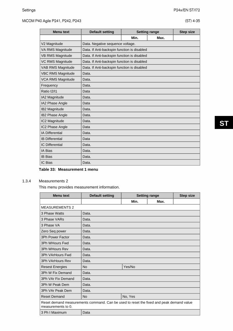
Settings
P24x/EN ST/I72 MiCOM P40 Agile P241, P242, P243 (ST) 4-35
ST
Menu text Default setting Setting range Step size Min. Max.
V2 Magnitude Data. Negative sequence voltage.
VA RMS Magnitude Data. If Anti-backspin function is disabled
VB RMS Magnitude Data. If Anti-backspin function is disabled
VC RMS Magnitude Data. If Anti-backspin function is disabled
VAB RMS Magnitude Data. If Anti-backspin function is disabled
VBC RMS Magnitude Data.
VCA RMS Magnitude Data.
Frequency Data.
Ratio I2/I1 Data
IA2 Magnitude Data.
IA2 Phase Angle Data
IB2 Magnitude Data.
IB2 Phase Angle Data.
IC2 Magnitude Data.
IC2 Phase Angle Data
IA Differential Data.
IB Differential Data
IC Differential Data.
IA Bias Data.
IB Bias Data.
IC Bias Data.
Table 33: Measurement 1 menu
1.3.4 Measurements 2 This menu provides measurement information.
Menu text Default setting Setting range Step size Min. Max.
MEASUREMENTS 2
3 Phase Watts Data.
3 Phase VARs Data.
3 Phase VA Data.
Zero Seq power Data.
3Ph Power Factor Data.
3Ph WHours Fwd Data.
3Ph WHours Rev Data.
3Ph VArHours Fwd Data.
3Ph VArHours Rev Data.
Resest Energies No Yes/No
3Ph W Fix Demand Data.
3Ph VAr Fix Demand Data.
3Ph W Peak Dem Data.
3Ph VAr Peak Dem Data.
Reset Demand No No, Yes
Reset demand measurements command. Can be used to reset the fixed and peak demand value measurements to 0.
3 Ph I Maximum Data
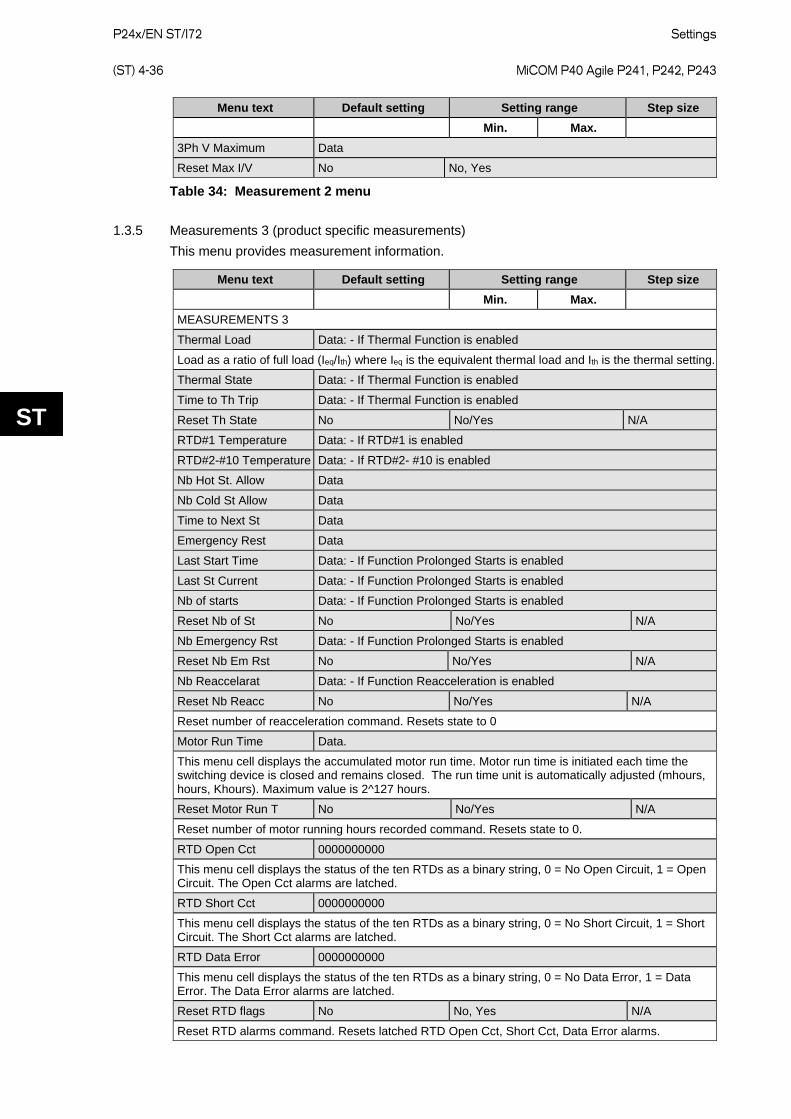
P24x/EN ST/I72
Settings (ST) 4-36 MiCOM P40 Agile P241, P242, P243
ST
Menu text Default setting Setting range Step size Min. Max.
3Ph V Maximum Data
Reset Max I/V No No, Yes
Table 34: Measurement 2 menu
1.3.5 Measurements 3 (product specific measurements) This menu provides measurement information.
Menu text Default setting Setting range Step size Min. Max.
MEASUREMENTS 3
Thermal Load Data: - If Thermal Function is enabled
Load as a ratio of full load (Ieq/Ith) where Ieq is the equivalent thermal load and Ith is the thermal setting.
Thermal State Data: - If Thermal Function is enabled
Time to Th Trip Data: - If Thermal Function is enabled
Reset Th State No No/Yes N/A
RTD#1 Temperature Data: - If RTD#1 is enabled
RTD#2-#10 Temperature Data: - If RTD#2- #10 is enabled
Nb Hot St. Allow Data
Nb Cold St Allow Data
Time to Next St Data
Emergency Rest Data
Last Start Time Data: - If Function Prolonged Starts is enabled
Last St Current Data: - If Function Prolonged Starts is enabled
Nb of starts Data: - If Function Prolonged Starts is enabled
Reset Nb of St No No/Yes N/A
Nb Emergency Rst Data: - If Function Prolonged Starts is enabled
Reset Nb Em Rst No No/Yes N/A
Nb Reaccelarat Data: - If Function Reacceleration is enabled
Reset Nb Reacc No No/Yes N/A
Reset number of reacceleration command. Resets state to 0
Motor Run Time Data.
This menu cell displays the accumulated motor run time. Motor run time is initiated each time the switching device is closed and remains closed. The run time unit is automatically adjusted (mhours, hours, Khours). Maximum value is 2^127 hours.
Reset Motor Run T No No/Yes N/A
Reset number of motor running hours recorded command. Resets state to 0.
RTD Open Cct 0000000000
This menu cell displays the status of the ten RTDs as a binary string, 0 = No Open Circuit, 1 = Open Circuit. The Open Cct alarms are latched.
RTD Short Cct 0000000000
This menu cell displays the status of the ten RTDs as a binary string, 0 = No Short Circuit, 1 = Short Circuit. The Short Cct alarms are latched.
RTD Data Error 0000000000
This menu cell displays the status of the ten RTDs as a binary string, 0 = No Data Error, 1 = Data Error. The Data Error alarms are latched.
Reset RTD flags No No, Yes N/A
Reset RTD alarms command. Resets latched RTD Open Cct, Short Cct, Data Error alarms.
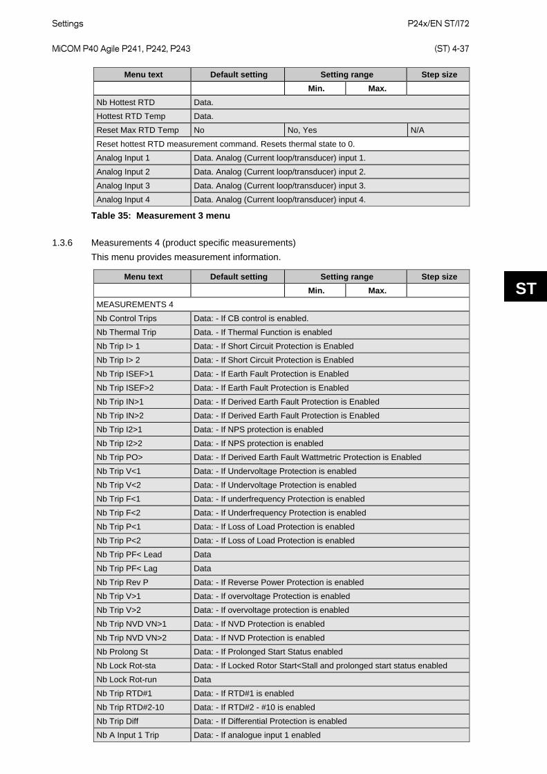
Settings
P24x/EN ST/I72 MiCOM P40 Agile P241, P242, P243 (ST) 4-37
ST
Menu text Default setting Setting range Step size Min. Max.
Nb Hottest RTD Data.
Hottest RTD Temp Data.
Reset Max RTD Temp No No, Yes N/A
Reset hottest RTD measurement command. Resets thermal state to 0.
Analog Input 1 Data. Analog (Current loop/transducer) input 1.
Analog Input 2 Data. Analog (Current loop/transducer) input 2.
Analog Input 3 Data. Analog (Current loop/transducer) input 3.
Analog Input 4 Data. Analog (Current loop/transducer) input 4.
Table 35: Measurement 3 menu
1.3.6 Measurements 4 (product specific measurements) This menu provides measurement information.
Menu text Default setting Setting range Step size Min. Max.
MEASUREMENTS 4
Nb Control Trips Data: - If CB control is enabled.
Nb Thermal Trip Data. - If Thermal Function is enabled
Nb Trip I> 1 Data: - If Short Circuit Protection is Enabled
Nb Trip I> 2 Data: - If Short Circuit Protection is Enabled
Nb Trip ISEF>1 Data: - If Earth Fault Protection is Enabled
Nb Trip ISEF>2 Data: - If Earth Fault Protection is Enabled
Nb Trip IN>1 Data: - If Derived Earth Fault Protection is Enabled
Nb Trip IN>2 Data: - If Derived Earth Fault Protection is Enabled
Nb Trip I2>1 Data: - If NPS protection is enabled
Nb Trip I2>2 Data: - If NPS protection is enabled
Nb Trip PO> Data: - If Derived Earth Fault Wattmetric Protection is Enabled
Nb Trip V<1 Data: - If Undervoltage Protection is enabled
Nb Trip V<2 Data: - If Undervoltage Protection is enabled
Nb Trip F<1 Data: - If underfrequency Protection is enabled
Nb Trip F<2 Data: - If Underfrequency Protection is enabled
Nb Trip P<1 Data: - If Loss of Load Protection is enabled
Nb Trip P<2 Data: - If Loss of Load Protection is enabled
Nb Trip PF< Lead Data
Nb Trip PF< Lag Data
Nb Trip Rev P Data: - If Reverse Power Protection is enabled
Nb Trip V>1 Data: - If overvoltage Protection is enabled
Nb Trip V>2 Data: - If overvoltage protection is enabled
Nb Trip NVD VN>1 Data: - If NVD Protection is enabled
Nb Trip NVD VN>2 Data: - If NVD Protection is enabled
Nb Prolong St Data: - If Prolonged Start Status enabled
Nb Lock Rot-sta Data: - If Locked Rotor Start<Stall and prolonged start status enabled
Nb Lock Rot-run Data
Nb Trip RTD#1 Data: - If RTD#1 is enabled
Nb Trip RTD#2-10 Data: - If RTD#2 - #10 is enabled
Nb Trip Diff Data: - If Differential Protection is enabled
Nb A Input 1 Trip Data: - If analogue input 1 enabled
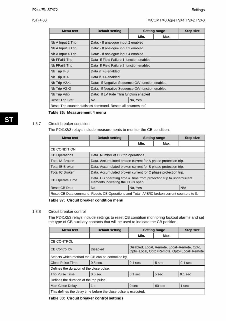
P24x/EN ST/I72
Settings (ST) 4-38 MiCOM P40 Agile P241, P242, P243
ST
Menu text Default setting Setting range Step size Min. Max.
Nb A Input 2 Trip Data: - If analogue input 2 enabled
Nb A Input 3 Trip Data: - If analogue input 3 enabled
Nb A Input 4 Trip Data: - If analogue input 4 enabled
Nb FFail1 Trip Data If Field Failure 1 function enabled
Nb FFail2 Trip Data If Field Failure 2 function enabled
Nb Trip I> 3 Data if I>3 enabled
Nb Trip I> 4 Data if I>4 enabled
Nb Trip V2>1 Data: If Negative Sequence O/V function enabled
Nb Trip V2>2 Data: If Negative Sequence O/V function enabled
Nb Trip Vdip Data: If LV Ride Thru function enabled
Reset Trip Stat No No, Yes
Reset Trip counter statistics command. Resets all counters to 0
Table 36: Measurement 4 menu
1.3.7 Circuit breaker condition The P241/2/3 relays include measurements to monitor the CB condition.
Menu text Default setting Setting range Step size Min. Max.
CB CONDITION
CB Operations Data. Number of CB trip operations.
Total IA Broken Data. Accumulated broken current for A phase protection trip.
Total IB Broken Data. Accumulated broken current for B phase protection trip.
Total IC Broken Data. Accumulated broken current for C phase protection trip.
CB Operate Time Data. CB operating time = time from protection trip to undercurrent elements indicating the CB is open.
Reset CB Data No No, Yes N/A
Reset CB Data command. Resets CB Operations and Total IA/IB/IC broken current counters to 0.
Table 37: Circuit breaker condition menu
1.3.8 Circuit breaker control The P241/2/3 relays include settings to reset CB condition monitoring lockout alarms and set the type of CB auxiliary contacts that will be used to indicate the CB position.
Menu text Default setting Setting range Step size Min. Max.
CB CONTROL
CB Control by Disabled Disabled, Local, Remote, Local+Remote, Opto, Opto+Local, Opto+Remote, Opto+Local+Remote
Selects which method the CB can be controlled by.
Close Pulse Time 0.5 sec 0.1 sec 5 sec 0.1 sec
Defines the duration of the close pulse.
Trip Pulse Time 0.5 sec 0.1 sec 5 sec 0.1 sec
Defines the duration of the trip pulse.
Man Close Delay 1 s 0 sec 60 sec 1 sec
This defines the delay time before the close pulse is executed.
Table 38: Circuit breaker control settings
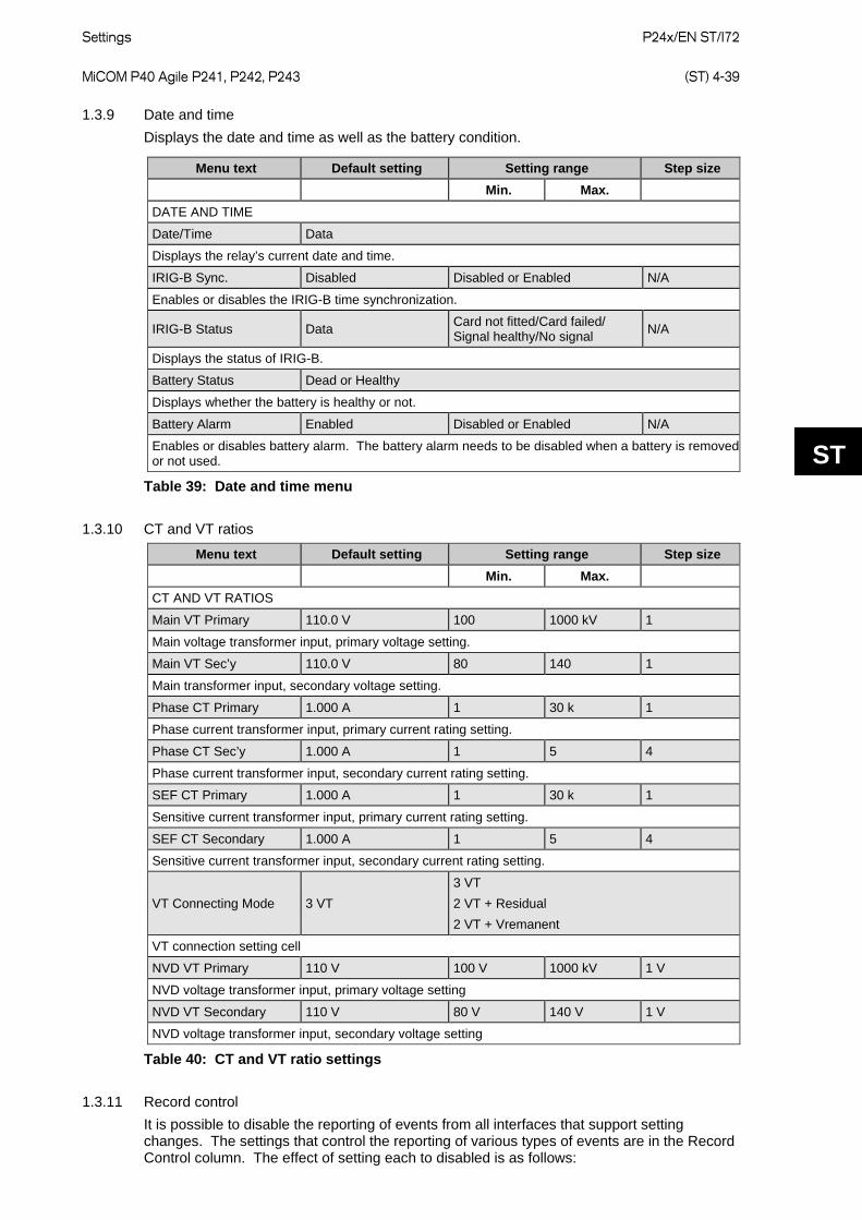
Settings
P24x/EN ST/I72 MiCOM P40 Agile P241, P242, P243 (ST) 4-39
ST
1.3.9 Date and time Displays the date and time as well as the battery condition.
Menu text Default setting Setting range Step size Min. Max.
DATE AND TIME
Date/Time Data
Displays the relay’s current date and time.
IRIG-B Sync. Disabled Disabled or Enabled N/A
Enables or disables the IRIG-B time synchronization.
IRIG-B Status Data Card not fitted/Card failed/ Signal healthy/No signal N/A
Displays the status of IRIG-B.
Battery Status Dead or Healthy
Displays whether the battery is healthy or not.
Battery Alarm Enabled Disabled or Enabled N/A
Enables or disables battery alarm. The battery alarm needs to be disabled when a battery is removed or not used.
Table 39: Date and time menu
1.3.10 CT and VT ratios
Menu text Default setting Setting range Step size Min. Max.
CT AND VT RATIOS
Main VT Primary 110.0 V 100 1000 kV 1
Main voltage transformer input, primary voltage setting.
Main VT Sec’y 110.0 V 80 140 1
Main transformer input, secondary voltage setting.
Phase CT Primary 1.000 A 1 30 k 1
Phase current transformer input, primary current rating setting.
Phase CT Sec’y 1.000 A 1 5 4
Phase current transformer input, secondary current rating setting.
SEF CT Primary 1.000 A 1 30 k 1
Sensitive current transformer input, primary current rating setting.
SEF CT Secondary 1.000 A 1 5 4
Sensitive current transformer input, secondary current rating setting.
VT Connecting Mode 3 VT 3 VT 2 VT + Residual 2 VT + Vremanent
VT connection setting cell
NVD VT Primary 110 V 100 V 1000 kV 1 V
NVD voltage transformer input, primary voltage setting
NVD VT Secondary 110 V 80 V 140 V 1 V
NVD voltage transformer input, secondary voltage setting
Table 40: CT and VT ratio settings
1.3.11 Record control It is possible to disable the reporting of events from all interfaces that support setting changes. The settings that control the reporting of various types of events are in the Record Control column. The effect of setting each to disabled is as follows:
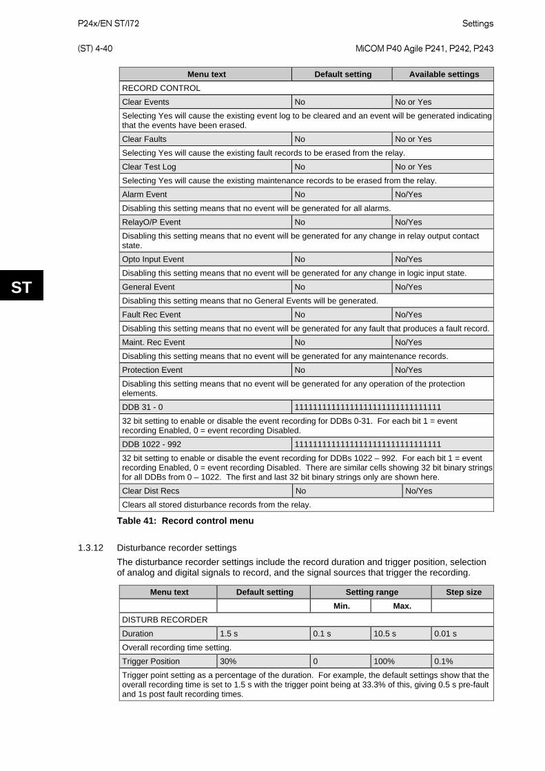
P24x/EN ST/I72
Settings (ST) 4-40 MiCOM P40 Agile P241, P242, P243
ST
Menu text Default setting Available settings RECORD CONTROL
Clear Events No No or Yes
Selecting Yes will cause the existing event log to be cleared and an event will be generated indicating that the events have been erased.
Clear Faults No No or Yes
Selecting Yes will cause the existing fault records to be erased from the relay.
Clear Test Log No No or Yes
Selecting Yes will cause the existing maintenance records to be erased from the relay.
Alarm Event No No/Yes
Disabling this setting means that no event will be generated for all alarms.
RelayO/P Event No No/Yes
Disabling this setting means that no event will be generated for any change in relay output contact state.
Opto Input Event No No/Yes
Disabling this setting means that no event will be generated for any change in logic input state.
General Event No No/Yes
Disabling this setting means that no General Events will be generated.
Fault Rec Event No No/Yes
Disabling this setting means that no event will be generated for any fault that produces a fault record.
Maint. Rec Event No No/Yes
Disabling this setting means that no event will be generated for any maintenance records.
Protection Event No No/Yes
Disabling this setting means that no event will be generated for any operation of the protection elements.
DDB 31 - 0 11111111111111111111111111111111
32 bit setting to enable or disable the event recording for DDBs 0-31. For each bit 1 = event recording Enabled, 0 = event recording Disabled.
DDB 1022 - 992 11111111111111111111111111111111
32 bit setting to enable or disable the event recording for DDBs 1022 – 992. For each bit 1 = event recording Enabled, 0 = event recording Disabled. There are similar cells showing 32 bit binary strings for all DDBs from 0 – 1022. The first and last 32 bit binary strings only are shown here.
Clear Dist Recs No No/Yes
Clears all stored disturbance records from the relay.
Table 41: Record control menu
1.3.12 Disturbance recorder settings The disturbance recorder settings include the record duration and trigger position, selection of analog and digital signals to record, and the signal sources that trigger the recording.
Menu text Default setting Setting range Step size Min. Max.
DISTURB RECORDER
Duration 1.5 s 0.1 s 10.5 s 0.01 s
Overall recording time setting.
Trigger Position 30% 0 100% 0.1%
Trigger point setting as a percentage of the duration. For example, the default settings show that the overall recording time is set to 1.5 s with the trigger point being at 33.3% of this, giving 0.5 s pre-fault and 1s post fault recording times.
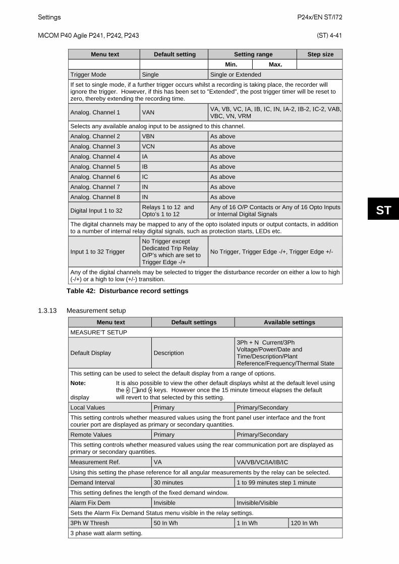
Settings
P24x/EN ST/I72 MiCOM P40 Agile P241, P242, P243 (ST) 4-41
ST
Menu text Default setting Setting range Step size Min. Max.
Trigger Mode Single Single or Extended
If set to single mode, if a further trigger occurs whilst a recording is taking place, the recorder will ignore the trigger. However, if this has been set to "Extended", the post trigger timer will be reset to zero, thereby extending the recording time.
Analog. Channel 1 VAN VA, VB, VC, ΙA, ΙB, ΙC, ΙN, ΙA-2, ΙB-2, ΙC-2, VAB, VBC, VN, VRM
Selects any available analog input to be assigned to this channel.
Analog. Channel 2 VBN As above
Analog. Channel 3 VCN As above
Analog. Channel 4 IA As above
Analog. Channel 5 IB As above
Analog. Channel 6 IC As above
Analog. Channel 7 IN As above
Analog. Channel 8 IN As above
Digital Input 1 to 32 Relays 1 to 12 and Opto’s 1 to 12
Any of 16 O/P Contacts or Any of 16 Opto Inputs or Internal Digital Signals
The digital channels may be mapped to any of the opto isolated inputs or output contacts, in addition to a number of internal relay digital signals, such as protection starts, LEDs etc.
Input 1 to 32 Trigger
No Trigger except Dedicated Trip Relay O/P’s which are set to Trigger Edge -/+
No Trigger, Trigger Edge -/+, Trigger Edge +/-
Any of the digital channels may be selected to trigger the disturbance recorder on either a low to high (-/+) or a high to low (+/-) transition.
Table 42: Disturbance record settings
1.3.13 Measurement setup
Menu text Default settings Available settings MEASURE’T SETUP
Default Display Description
3Ph + N Current/3Ph Voltage/Power/Date and Time/Description/Plant Reference/Frequency/Thermal State
This setting can be used to select the default display from a range of options. Note: It is also possible to view the other default displays whilst at the default level using the and keys. However once the 15 minute timeout elapses the default display will revert to that selected by this setting.
Local Values Primary Primary/Secondary
This setting controls whether measured values using the front panel user interface and the front courier port are displayed as primary or secondary quantities.
Remote Values Primary Primary/Secondary
This setting controls whether measured values using the rear communication port are displayed as primary or secondary quantities.
Measurement Ref. VA VA/VB/VC/ΙA/ΙB/ΙC
Using this setting the phase reference for all angular measurements by the relay can be selected.
Demand Interval 30 minutes 1 to 99 minutes step 1 minute
This setting defines the length of the fixed demand window.
Alarm Fix Dem Invisible Invisible/Visible
Sets the Alarm Fix Demand Status menu visible in the relay settings.
3Ph W Thresh 50 In Wh 1 In Wh 120 In Wh
3 phase watt alarm setting.
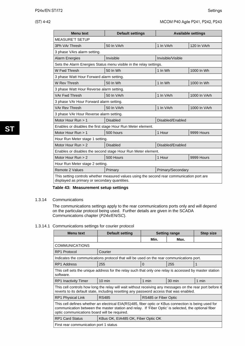
P24x/EN ST/I72
Settings (ST) 4-42 MiCOM P40 Agile P241, P242, P243
ST
Menu text Default settings Available settings MEASURE’T SETUP
3Ph VAr Thresh 50 In VArh 1 In VArh 120 In VArh
3 phase VArs alarm setting.
Alarm Energies Invisible Invisible/Visible
Sets the Alarm Energies Status menu visible in the relay settings.
W Fwd Thresh 50 In Wh 1 In Wh 1000 In Wh
3 phase Watt Hour Forward alarm setting.
W Rev Thresh 50 In Wh 1 In Wh 1000 In Wh
3 phase Watt Hour Reverse alarm setting.
VAr Fwd Thresh 50 In VArh 1 In VArh 1000 In VArh
3 phase VAr Hour Forward alarm setting.
VAr Rev Thresh 50 In VArh 1 In VArh 1000 In VArh
3 phase VAr Hour Reverse alarm setting.
Motor Hour Run > 1 Disabled Disabled/Enabled
Enables or disables the first stage Hour Run Meter element.
Motor Hour Run > 1 500 hours 1 Hour 9999 Hours
Hour Run Meter stage 1 setting.
Motor Hour Run > 2 Disabled Disabled/Enabled
Enables or disables the second stage Hour Run Meter element.
Motor Hour Run > 2 500 Hours 1 Hour 9999 Hours
Hour Run Meter stage 2 setting.
Remote 2 Values Primary Primary/Secondary
This setting controls whether measured values using the second rear communication port are displayed as primary or secondary quantities.
Table 43: Measurement setup settings
1.3.14 Communications The communications settings apply to the rear communications ports only and will depend on the particular protocol being used. Further details are given in the SCADA Communications chapter (P24x/EN/SC).
1.3.14.1 Communications settings for courier protocol
Menu text Default setting Setting range Step size Min. Max.
COMMUNICATIONS
RP1 Protocol Courier
Indicates the communications protocol that will be used on the rear communications port.
RP1 Address 255 0 255 1
This cell sets the unique address for the relay such that only one relay is accessed by master station software.
RP1 Inactivity Timer 10 min 1 min 30 min 1 min
This cell controls how long the relay will wait without receiving any messages on the rear port before it reverts to its default state, including resetting any password access that was enabled.
RP1 Physical Link RS485 RS485 or Fiber Optic
This cell defines whether an electrical EIA(RS)485, fiber optic or KBus connection is being used for communication between the master station and relay. If ‘Fiber Optic’ is selected, the optional fiber optic communications board will be required.
RP1 Card Status KBus OK, EIA485 OK, Fiber Optic OK
First rear communication port 1 status

Settings
P24x/EN ST/I72 MiCOM P40 Agile P241, P242, P243 (ST) 4-43
ST
Menu text Default setting Setting range Step size Min. Max.
RP1 Port Config. Kbus Kbus, EAI(RS)485
This cell defines whether an electrical KBus or EIA(RS)485 is being used for communication between the master station and relay.
RP1 Comms Mode IEC 60870 FT1.2 IEC 60870 FT1.2, 10Bit
The choice is either IEC 60870 FT1.2 for normal operation with 11-bit modems, or 10-bit no parity.
RP1 Baud Rate 19200 bits/s 9600 bits/s, 19200 bits/s or 38400 bits/s
This cell controls the communication speed between relay and master station. It is important that both relay and master station are set at the same speed setting.
Table 44: Communication settings for courier protocol
1.3.14.2 Communications settings for MODBUS protocol
Menu text Default setting Setting range Step size Min. Max.
COMMUNICATIONS
RP1 Protocol MODBUS
Indicates the communications protocol that will be used on the rear communications port.
RP1 Address 1 1 247 1
This cell sets the unique address for the relay such that only one relay is accessed by master station software.
RP1 Inactiv Timer 10 mins. 1 min. 30 mins. 1 min.
This cell controls how long the relay will wait without receiving any messages on the rear port before it reverts to its default state, including resetting any password access that was enabled.
RP1 Baud Rate 19200 bits/s 9600 bits/s, 19200 bits/s or 38400 bits/s
This cell controls the communication speed between relay and master station. It is important that both relay and master station are set at the same speed setting.
RP1 Parity None Odd, Even or None
This cell controls the parity format used in the data frames. It is important that both relay and master station are set with the same parity setting.
RP1 Physical Link RS485 RS485 or Fiber Optic
This cell defines whether an electrical EIA(RS) 485 or fiber optic connection is being used for communication between the master station and relay. If Fiber Optic is selected, the optional fiber optic communications board will be required.
MODBUS IEC Time Standard IEC Standard IEC or Reverse
When Standard IEC is selected the time format complies with IEC 60870-5-4 requirements such that byte 1 of the information is transmitted first, followed by bytes 2 through to 7. If Reverse is selected the transmission of information is reversed.
Table 45: Communication settings for MODBUS protocol
1.3.14.3 Communications settings for IEC 60870-5-103 protocol
Menu text Default setting Setting range Step size Min. Max.
COMMUNICATIONS
RP1 Protocol IEC 60870-5-103
Indicates the communications protocol that will be used on the rear communications port.
RP1 Address 1 0 254 1
This cell sets the unique address for the relay such that only one relay is accessed by master station software.
RP1 Inactiv Timer 15 mins. 1 min. 30 mins. 1 min.
This cell controls how long the relay will wait without receiving any messages on the rear port before it reverts to its default state, including resetting any password access that was enabled.
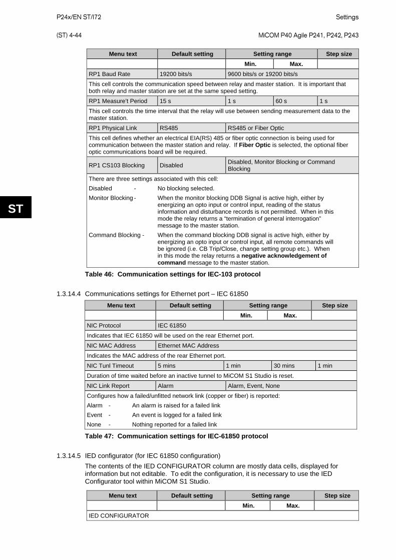
P24x/EN ST/I72
Settings (ST) 4-44 MiCOM P40 Agile P241, P242, P243
ST
Menu text Default setting Setting range Step size Min. Max.
RP1 Baud Rate 19200 bits/s 9600 bits/s or 19200 bits/s
This cell controls the communication speed between relay and master station. It is important that both relay and master station are set at the same speed setting.
RP1 Measure’t Period 15 s 1 s 60 s 1 s
This cell controls the time interval that the relay will use between sending measurement data to the master station.
RP1 Physical Link RS485 RS485 or Fiber Optic
This cell defines whether an electrical EIA(RS) 485 or fiber optic connection is being used for communication between the master station and relay. If Fiber Optic is selected, the optional fiber optic communications board will be required.
RP1 CS103 Blocking Disabled Disabled, Monitor Blocking or Command Blocking
There are three settings associated with this cell: Disabled - No blocking selected. Monitor Blocking - When the monitor blocking DDB Signal is active high, either by energizing an opto input or control input, reading of the status information and disturbance records is not permitted. When in this mode the relay returns a “termination of general interrogation” message to the master station. Command Blocking - When the command blocking DDB signal is active high, either by energizing an opto input or control input, all remote commands will be ignored (i.e. CB Trip/Close, change setting group etc.). When in this mode the relay returns a negative acknowledgement of command message to the master station.
Table 46: Communication settings for IEC-103 protocol
1.3.14.4 Communications settings for Ethernet port – IEC 61850
Menu text Default setting Setting range Step size Min. Max.
NIC Protocol IEC 61850
Indicates that IEC 61850 will be used on the rear Ethernet port.
NIC MAC Address Ethernet MAC Address
Indicates the MAC address of the rear Ethernet port.
NIC Tunl Timeout 5 mins 1 min 30 mins 1 min
Duration of time waited before an inactive tunnel to MiCOM S1 Studio is reset.
NIC Link Report Alarm Alarm, Event, None
Configures how a failed/unfitted network link (copper or fiber) is reported: Alarm - An alarm is raised for a failed link Event - An event is logged for a failed link None - Nothing reported for a failed link
Table 47: Communication settings for IEC-61850 protocol
1.3.14.5 IED configurator (for IEC 61850 configuration) The contents of the IED CONFIGURATOR column are mostly data cells, displayed for information but not editable. To edit the configuration, it is necessary to use the IED Configurator tool within MiCOM S1 Studio.
Menu text Default setting Setting range Step size Min. Max.
IED CONFIGURATOR
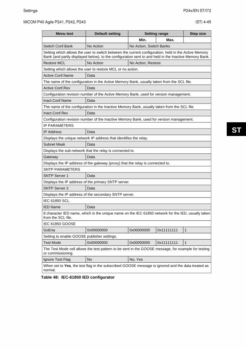
Settings
P24x/EN ST/I72 MiCOM P40 Agile P241, P242, P243 (ST) 4-45
ST
Menu text Default setting Setting range Step size Min. Max.
Switch Conf.Bank No Action No Action, Switch Banks
Setting which allows the user to switch between the current configuration, held in the Active Memory Bank (and partly displayed below), to the configuration sent to and held in the Inactive Memory Bank.
Restore MCL No Action No Action, Restore
Setting which allows the user to restore MCL or no action.
Active Conf.Name Data
The name of the configuration in the Active Memory Bank, usually taken from the SCL file.
Active Conf.Rev Data
Configuration revision number of the Active Memory Bank, used for version management.
Inact.Conf.Name Data
The name of the configuration in the Inactive Memory Bank, usually taken from the SCL file.
Inact.Conf.Rev Data
Configuration revision number of the Inactive Memory Bank, used for version management.
IP PARAMETERS
IP Address Data
Displays the unique network IP address that identifies the relay.
Subnet Mask Data
Displays the sub-network that the relay is connected to.
Gateway Data
Displays the IP address of the gateway (proxy) that the relay is connected to.
SNTP PARAMETERS
SNTP Server 1 Data
Displays the IP address of the primary SNTP server.
SNTP Server 2 Data
Displays the IP address of the secondary SNTP server.
IEC 61850 SCL.
IED Name Data
8 character IED name, which is the unique name on the IEC 61850 network for the IED, usually taken from the SCL file.
IEC 61850 GOOSE
GoEna 0x00000000 0x00000000 0x11111111 1
Setting to enable GOOSE publisher settings.
Test Mode 0x00000000 0x00000000 0x11111111 1
The Test Mode cell allows the test pattern to be sent in the GOOSE message, for example for testing or commissioning.
Ignore Test Flag No No, Yes
When set to Yes, the test flag in the subscribed GOOSE message is ignored and the data treated as normal.
Table 48: IEC-61850 IED configurator
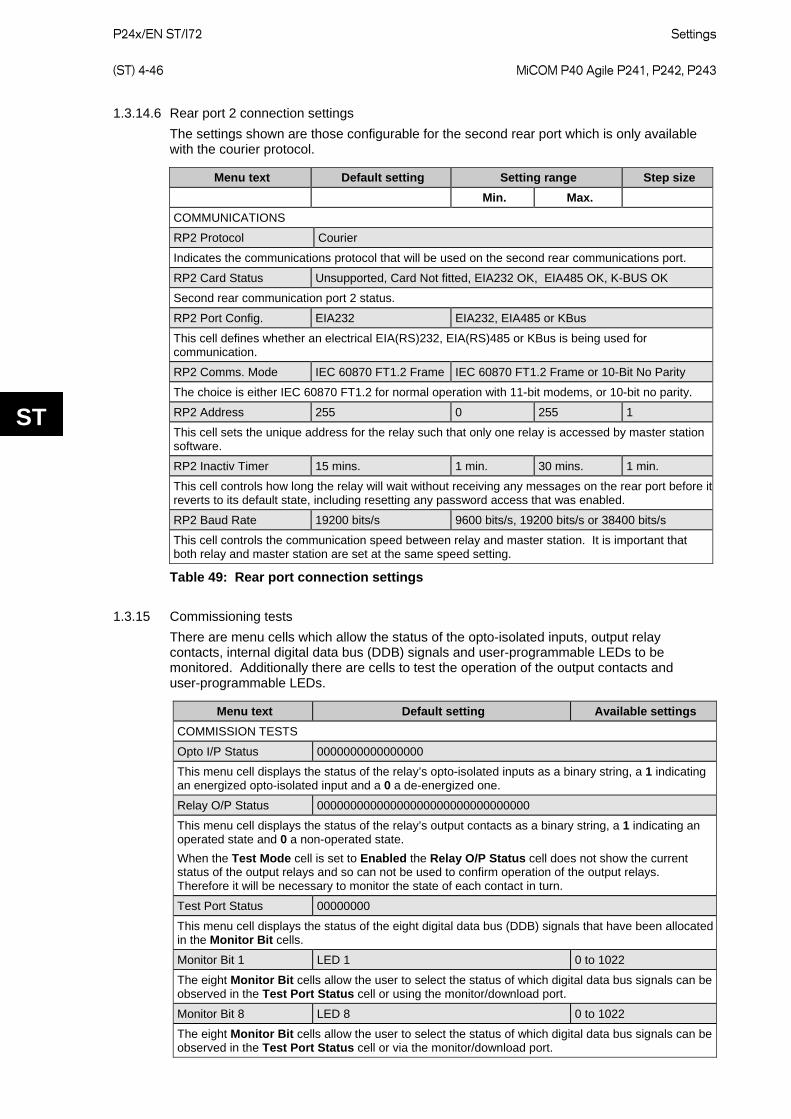
P24x/EN ST/I72
Settings (ST) 4-46 MiCOM P40 Agile P241, P242, P243
ST
1.3.14.6 Rear port 2 connection settings The settings shown are those configurable for the second rear port which is only available with the courier protocol.
Menu text Default setting Setting range Step size Min. Max.
COMMUNICATIONS
RP2 Protocol Courier
Indicates the communications protocol that will be used on the second rear communications port.
RP2 Card Status Unsupported, Card Not fitted, EIA232 OK, EIA485 OK, K-BUS OK
Second rear communication port 2 status.
RP2 Port Config. EIA232 EIA232, EIA485 or KBus
This cell defines whether an electrical EIA(RS)232, EIA(RS)485 or KBus is being used for communication.
RP2 Comms. Mode IEC 60870 FT1.2 Frame IEC 60870 FT1.2 Frame or 10-Bit No Parity
The choice is either IEC 60870 FT1.2 for normal operation with 11-bit modems, or 10-bit no parity.
RP2 Address 255 0 255 1
This cell sets the unique address for the relay such that only one relay is accessed by master station software.
RP2 Inactiv Timer 15 mins. 1 min. 30 mins. 1 min.
This cell controls how long the relay will wait without receiving any messages on the rear port before it reverts to its default state, including resetting any password access that was enabled.
RP2 Baud Rate 19200 bits/s 9600 bits/s, 19200 bits/s or 38400 bits/s
This cell controls the communication speed between relay and master station. It is important that both relay and master station are set at the same speed setting.
Table 49: Rear port connection settings
1.3.15 Commissioning tests There are menu cells which allow the status of the opto-isolated inputs, output relay contacts, internal digital data bus (DDB) signals and user-programmable LEDs to be monitored. Additionally there are cells to test the operation of the output contacts and user-programmable LEDs.
Menu text Default setting Available settings COMMISSION TESTS
Opto I/P Status 0000000000000000
This menu cell displays the status of the relay’s opto-isolated inputs as a binary string, a 1 indicating an energized opto-isolated input and a 0 a de-energized one.
Relay O/P Status 00000000000000000000000000000000
This menu cell displays the status of the relay’s output contacts as a binary string, a 1 indicating an operated state and 0 a non-operated state. When the Test Mode cell is set to Enabled the Relay O/P Status cell does not show the current status of the output relays and so can not be used to confirm operation of the output relays. Therefore it will be necessary to monitor the state of each contact in turn.
Test Port Status 00000000
This menu cell displays the status of the eight digital data bus (DDB) signals that have been allocated in the Monitor Bit cells.
Monitor Bit 1 LED 1 0 to 1022
The eight Monitor Bit cells allow the user to select the status of which digital data bus signals can be observed in the Test Port Status cell or using the monitor/download port.
Monitor Bit 8 LED 8 0 to 1022
The eight Monitor Bit cells allow the user to select the status of which digital data bus signals can be observed in the Test Port Status cell or via the monitor/download port.
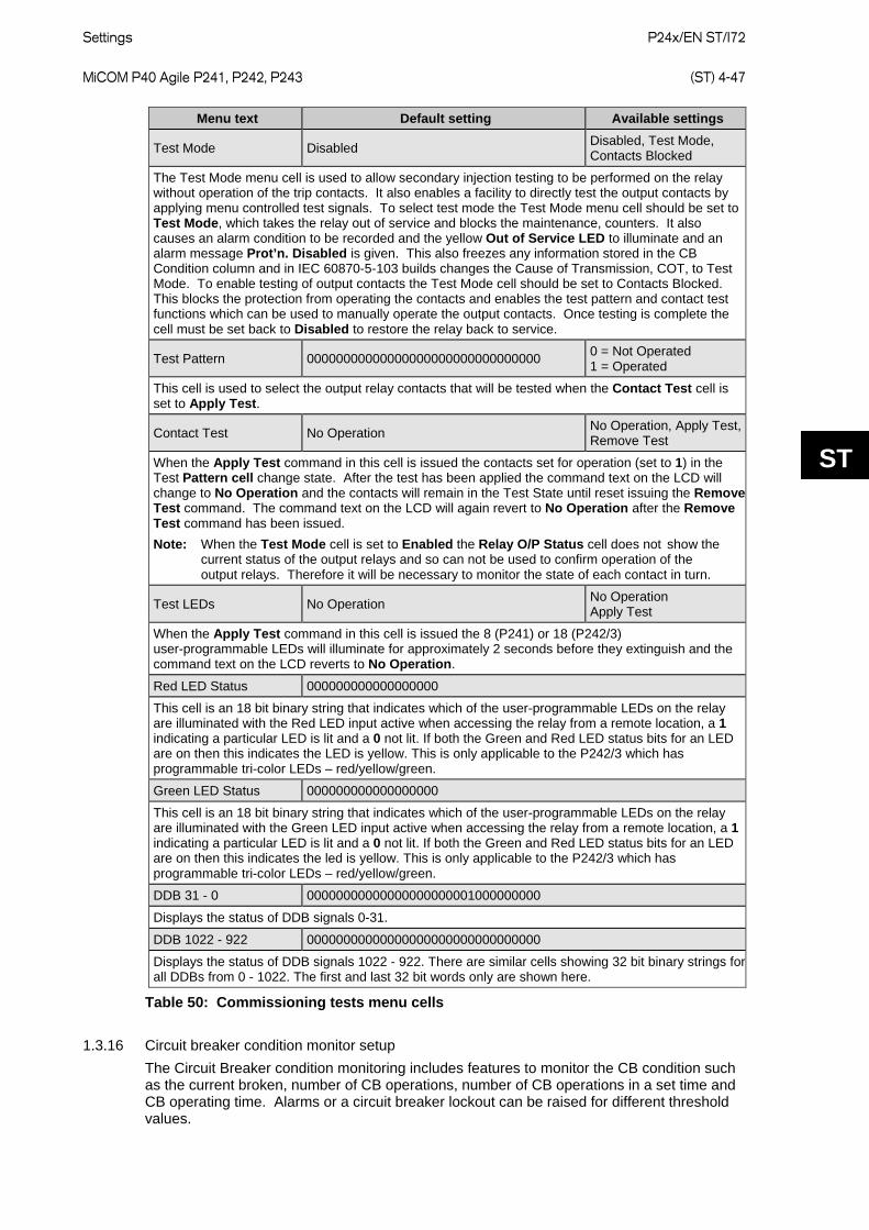
Settings
P24x/EN ST/I72 MiCOM P40 Agile P241, P242, P243 (ST) 4-47
ST
Menu text Default setting Available settings
Test Mode Disabled Disabled, Test Mode, Contacts Blocked
The Test Mode menu cell is used to allow secondary injection testing to be performed on the relay without operation of the trip contacts. It also enables a facility to directly test the output contacts by applying menu controlled test signals. To select test mode the Test Mode menu cell should be set to Test Mode, which takes the relay out of service and blocks the maintenance, counters. It also causes an alarm condition to be recorded and the yellow Out of Service LED to illuminate and an alarm message Prot’n. Disabled is given. This also freezes any information stored in the CB Condition column and in IEC 60870-5-103 builds changes the Cause of Transmission, COT, to Test Mode. To enable testing of output contacts the Test Mode cell should be set to Contacts Blocked. This blocks the protection from operating the contacts and enables the test pattern and contact test functions which can be used to manually operate the output contacts. Once testing is complete the cell must be set back to Disabled to restore the relay back to service.
Test Pattern 00000000000000000000000000000000 0 = Not Operated 1 = Operated
This cell is used to select the output relay contacts that will be tested when the Contact Test cell is set to Apply Test.
Contact Test No Operation No Operation, Apply Test, Remove Test
When the Apply Test command in this cell is issued the contacts set for operation (set to 1) in the Test Pattern cell change state. After the test has been applied the command text on the LCD will change to No Operation and the contacts will remain in the Test State until reset issuing the Remove Test command. The command text on the LCD will again revert to No Operation after the Remove Test command has been issued. Note: When the Test Mode cell is set to Enabled the Relay O/P Status cell does not show the current status of the output relays and so can not be used to confirm operation of the output relays. Therefore it will be necessary to monitor the state of each contact in turn.
Test LEDs No Operation No Operation Apply Test
When the Apply Test command in this cell is issued the 8 (P241) or 18 (P242/3) user-programmable LEDs will illuminate for approximately 2 seconds before they extinguish and the command text on the LCD reverts to No Operation.
Red LED Status 000000000000000000
This cell is an 18 bit binary string that indicates which of the user-programmable LEDs on the relay are illuminated with the Red LED input active when accessing the relay from a remote location, a 1 indicating a particular LED is lit and a 0 not lit. If both the Green and Red LED status bits for an LED are on then this indicates the LED is yellow. This is only applicable to the P242/3 which has programmable tri-color LEDs – red/yellow/green.
Green LED Status 000000000000000000
This cell is an 18 bit binary string that indicates which of the user-programmable LEDs on the relay are illuminated with the Green LED input active when accessing the relay from a remote location, a 1 indicating a particular LED is lit and a 0 not lit. If both the Green and Red LED status bits for an LED are on then this indicates the led is yellow. This is only applicable to the P242/3 which has programmable tri-color LEDs – red/yellow/green.
DDB 31 - 0 00000000000000000000001000000000
Displays the status of DDB signals 0-31.
DDB 1022 - 922 00000000000000000000000000000000
Displays the status of DDB signals 1022 - 922. There are similar cells showing 32 bit binary strings for all DDBs from 0 - 1022. The first and last 32 bit words only are shown here.
Table 50: Commissioning tests menu cells
1.3.16 Circuit breaker condition monitor setup The Circuit Breaker condition monitoring includes features to monitor the CB condition such as the current broken, number of CB operations, number of CB operations in a set time and CB operating time. Alarms or a circuit breaker lockout can be raised for different threshold values.
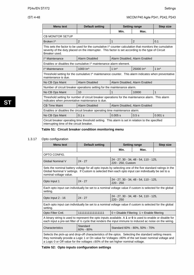
P24x/EN ST/I72
Settings (ST) 4-48 MiCOM P40 Agile P241, P242, P243
ST
Menu text Default setting Setting range Step size Min. Max.
CB MONITOR SETUP
Broken Ι^ 2 1 2 0.1
This sets the factor to be used for the cumulative Ι^ counter calculation that monitors the cumulative severity of the duty placed on the interrupter. This factor is set according to the type of Circuit Breaker used.
Ι^ Maintenance Alarm Disabled Alarm Disabled, Alarm Enabled
Enables or disables the cumulative Ι^ maintenance alarm element.
Ι^ Maintenance 1000 Ιn^ 1 Ιn^ 25000 Ιn^ 1 Ιn^
Threshold setting for the cumulative Ι^ maintenance counter. This alarm indicates when preventative maintenance is due.
No CB Ops Maint Alarm Disabled Alarm Disabled, Alarm Enabled
Number of circuit breaker operations setting for the maintenance alarm.
No CB Ops Maint 10 1 10000 1
Threshold setting for number of circuit breaker operations for the maintenance alarm. This alarm indicates when preventative maintenance is due.
CB Time Maint Alarm Disabled Alarm Disabled, Alarm Enabled
Enables or disables the circuit breaker operating time maintenance alarm.
No CB Ops Maint 0.1 s 0.005 s 0.5 s 0.001 s
Circuit breaker operating time threshold setting. This alarm is set in relation to the specified interrupting time of the circuit breaker.
Table 51: Circuit breaker condition monitoring menu
1.3.17 Opto configuration
Menu text Default setting Setting range Step size Min. Max.
OPTO CONFIG.
Global Nominal V 24 - 27 24 - 27, 30 - 34, 48 - 54, 110 - 125, 220 - 250, Custom
Sets the nominal battery voltage for all opto inputs by selecting one of the five standard ratings in the Global Nominal V settings. If Custom is selected then each opto input can individually be set to a nominal voltage value.
Opto Input 1 24 - 27 24 - 27, 30 - 34, 48 - 54, 110 - 125, 220 - 250
Each opto input can individually be set to a nominal voltage value if custom is selected for the global setting.
Opto Input 2 - 16 24 - 27 24 - 27, 30 - 34, 48 - 54, 110 - 125, 220 - 250
Each opto input can individually be set to a nominal voltage value if custom is selected for the global setting.
Opto Filter Cntl. 1111111111111111 0 = Disable Filtering 1 = Enable filtering
A binary string is used to represent the opto inputs available. A 1 or 0 is used to enable or disable for each input a pre-set filter of ½ cycle that renders the input immune to induced ac noise on the wiring.
Characteristics Standard 60% - 80% Standard 60% - 80%, 50% - 70%
Selects the pick-up and drop-off characteristics of the optos. Selecting the standard setting means they nominally provide a Logic 1 or On value for Voltages ≥80% of the set lower nominal voltage and a Logic 0 or Off value for the voltages ≤60% of the set higher nominal voltage.
Table 52: Opto inputs configuration settings
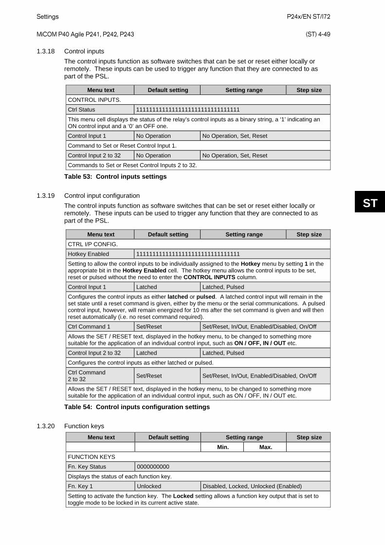
Settings
P24x/EN ST/I72 MiCOM P40 Agile P241, P242, P243 (ST) 4-49
ST
1.3.18 Control inputs The control inputs function as software switches that can be set or reset either locally or remotely. These inputs can be used to trigger any function that they are connected to as part of the PSL.
Menu text Default setting Setting range Step size CONTROL INPUTS.
Ctrl Status 11111111111111111111111111111111
This menu cell displays the status of the relay’s control inputs as a binary string, a ‘1’ indicating an ON control input and a ‘0’ an OFF one.
Control Input 1 No Operation No Operation, Set, Reset
Command to Set or Reset Control Input 1.
Control Input 2 to 32 No Operation No Operation, Set, Reset
Commands to Set or Reset Control Inputs 2 to 32.
Table 53: Control inputs settings
1.3.19 Control input configuration The control inputs function as software switches that can be set or reset either locally or remotely. These inputs can be used to trigger any function that they are connected to as part of the PSL.
Menu text Default setting Setting range Step size CTRL I/P CONFIG.
Hotkey Enabled 11111111111111111111111111111111
Setting to allow the control inputs to be individually assigned to the Hotkey menu by setting 1 in the appropriate bit in the Hotkey Enabled cell. The hotkey menu allows the control inputs to be set, reset or pulsed without the need to enter the CONTROL INPUTS column.
Control Input 1 Latched Latched, Pulsed
Configures the control inputs as either latched or pulsed. A latched control input will remain in the set state until a reset command is given, either by the menu or the serial communications. A pulsed control input, however, will remain energized for 10 ms after the set command is given and will then reset automatically (i.e. no reset command required).
Ctrl Command 1 Set/Reset Set/Reset, In/Out, Enabled/Disabled, On/Off
Allows the SET / RESET text, displayed in the hotkey menu, to be changed to something more suitable for the application of an individual control input, such as ON / OFF, IN / OUT etc.
Control Input 2 to 32 Latched Latched, Pulsed
Configures the control inputs as either latched or pulsed.
Ctrl Command 2 to 32 Set/Reset Set/Reset, In/Out, Enabled/Disabled, On/Off
Allows the SET / RESET text, displayed in the hotkey menu, to be changed to something more suitable for the application of an individual control input, such as ON / OFF, IN / OUT etc.
Table 54: Control inputs configuration settings
1.3.20 Function keys
Menu text Default setting Setting range Step size Min. Max.
FUNCTION KEYS
Fn. Key Status 0000000000
Displays the status of each function key.
Fn. Key 1 Unlocked Disabled, Locked, Unlocked (Enabled)
Setting to activate the function key. The Locked setting allows a function key output that is set to toggle mode to be locked in its current active state.
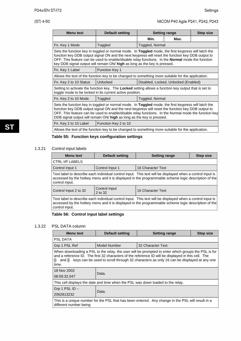
P24x/EN ST/I72
Settings (ST) 4-50 MiCOM P40 Agile P241, P242, P243
ST
Menu text Default setting Setting range Step size Min. Max.
Fn. Key 1 Mode Toggled Toggled, Normal
Sets the function key in toggled or normal mode. In Toggled mode, the first keypress will latch the function key DDB output signal ON and the next keypress will reset the function key DDB output to OFF. This feature can be used to enable/disable relay functions. In the Normal mode the function key DDB signal output will remain ON/ high as long as the key is pressed.
Fn. Key 1 Label Function Key 1
Allows the text of the function key to be changed to something more suitable for the application.
Fn. Key 2 to 10 Status Unlocked Disabled, Locked, Unlocked (Enabled)
Setting to activate the function key. The Locked setting allows a function key output that is set to toggle mode to be locked in its current active position.
Fn. Key 2 to 10 Mode Toggled Toggled, Normal
Sets the function key in toggled or normal mode. In Toggled mode, the first keypress will latch the function key DDB output signal ON and the next keypress will reset the function key DDB output to OFF. This feature can be used to enable/disable relay functions. In the Normal mode the function key DDB signal output will remain ON/ high as long as the key is pressed.
Fn. Key 2 to 10 Label Function Key 2 to 10
Allows the text of the function key to be changed to something more suitable for the application.
Table 55: Function keys configuration settings
1.3.21 Control input labels
Menu text Default setting Setting range Step size CTRL I/P LABELS
Control Input 1 Control Input 1 16 Character Text
Text label to describe each individual control input. This text will be displayed when a control input is accessed by the hotkey menu and it is displayed in the programmable scheme logic description of the control input.
Control Input 2 to 32 Control Input 2 to 32 16 Character Text
Text label to describe each individual control input. This text will be displayed when a control input is accessed by the hotkey menu and it is displayed in the programmable scheme logic description of the control input.
Table 56: Control input label settings
1.3.22 PSL DATA column
Menu text Default setting Setting range Step size PSL DATA
Grp 1 PSL Ref Model Number 32 Character Text
When downloading a PSL to the relay, the user will be prompted to enter which groups the PSL is for and a reference ID. The first 32 characters of the reference ID will be displayed in this cell. The and keys can be used to scroll through 32 characters as only 16 can be displayed at any one time.
18 Nov 2002 08:59:32.047
Data.
This cell displays the date and time when the PSL was down loaded to the relay.
Grp 1 PSL ID – 2062813232
Data.
This is a unique number for the PSL that has been entered. Any change in the PSL will result in a different number being
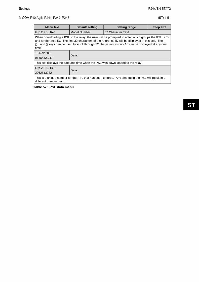
Settings
P24x/EN ST/I72 MiCOM P40 Agile P241, P242, P243 (ST) 4-51
ST
Menu text Default setting Setting range Step size Grp 2 PSL Ref Model Number 32 Character Text
When downloading a PSL to the relay, the user will be prompted to enter which groups the PSL is for and a reference ID. The first 32 characters of the reference ID will be displayed in this cell. The and keys can be used to scroll through 32 characters as only 16 can be displayed at any one time.
18 Nov 2002 08:59:32.047
Data.
This cell displays the date and time when the PSL was down loaded to the relay.
Grp 2 PSL ID – 2062813232
Data.
This is a unique number for the PSL that has been entered. Any change in the PSL will result in a different number being
Table 57: PSL data menu

P24x/EN ST/I72
Settings (ST) 4-52 MiCOM P40 Agile P241, P242, P243
ST
Operation
P24x/EN OP/I72 MiCOM P40 Agile P241, P242, P243 (OP) 5-1
OP
OPERATION

P24x/EN OP/I72
Operation (OP) 5-2 MiCOM P40 Agile P241, P242, P243
OP
Operation
P24x/EN OP/I72 MiCOM P40 Agile P241, P242, P243 (OP) 5-3
OP
CONTENTS
1 OPERATION OF INDIVIDUAL PROTECTION FUNCTIONS 9 1.1 Motor starting and running (stall protection) (48/51LR/50S/14) 9 1.1.1 Stall protection description 9 1.1.1.1 Prolonged start 9 1.1.1.2 Locked rotor during starting – (stall time < start time) 10 1.1.1.3 Stall during running 10 1.1.1.4 Momentary reduction in system voltage during running 11 1.1.1.5 Reacceleration after a reduction in system voltage 11 1.1.1.6 Low voltage ride through authorization 11 1.1.1.7 Auto Re-start authorization: re-start/load restoration sequence 13 1.2 Number of starts limitation (66) 15 1.2.1 Starts inhibition 15 1.2.2 Time between starts 17 1.3 Anti-Backspin protection (27 remanent) 18 1.3.1 Anti-Backspin description 18 1.3.1.1 2 VT + Vremanent is connected: 19 1.4 Thermal overload (49) 19 1.4.1 Thermal replica 19 1.4.2 Thermal trip 20 1.4.2.1 Compensation for ambient temperature by RTD 20 1.4.2.2 Motor thermal state 21 1.4.2.3 Thermal lockout 22 1.4.2.4 Emergency restart 22 1.4.2.5 User programmable curve for thermal over load protection 23 1.5 Motor differential protection (87) 23 1.5.1 Biased differential protection 24 1.5.1.1 Differential and bias current calculation 25 1.5.2 High impedance differential protection 27 1.5.3 Self balance winding differential 29 1.6 Short circuit protection (50/51) 30 1.6.1 RI curve 32 1.6.2 Timer hold facility 32 1.6.3 User programmable overcurrent protection 33 1.7 Negative sequence overcurrent protection (NPS) (46) 34 1.8 Voltage elements (27/59/59N) 34 1.8.1 Undervoltage protection (27) 34 1.8.2 Overvoltage protection (59) 35 1.8.3 Negative Sequence Overvoltage (47) 36
P24x/EN OP/I72
Operation (OP) 5-4 MiCOM P40 Agile P241, P242, P243
OP
1.8.4 3 Phase voltage checking (47/27) 36 1.8.5 Residual overvoltage / NVD protection (59N) 36 1.9 Underfrequency protection (81U) 39 1.10 Field failure protection function (40) 39 1.11 Power elements (32R/37/55) 41 1.11.1 Reverse power (32R) 41 1.11.2 Out of step protection (under power factor) (55) 42 1.11.2.1 Principle 42 1.11.2.2 Feature description 42 1.11.3 Loss of load (under power) (37) 42 1.12 Sensitive earth fault protection function (50N/51N/67N/32N/64N) 43 1.12.1 User programmable sensitive earth fault protection 46 1.13 Derived earth fault protection function (50N/51N) 46 1.13.1 User programmable derived earth fault protection 48 1.14 Resistive temperature device (RTD) thermal protection 48 1.14.1 Principle of the RTD connection 49 1.15 Circuit breaker failure protection (50BF) 50 1.16 Current loop inputs and outputs 51 1.16.1 Current loop inputs 51 1.16.2 Current loop output 53
2 OPERATION OF NON PROTECTION FUNCTIONS 57 2.1 VT supervision 57 2.1.1 Loss of all three-phase voltages under load conditions 57 2.1.2 Absence of three-phase voltages on line energization 57 2.1.2.1 Inputs 58 2.1.3 Operation 59 2.2 CT supervision 59 2.3 Circuit breaker state monitoring 60 2.4 Circuit breaker condition monitoring 62 2.4.1 Circuit breaker condition monitoring features 62 2.5 Circuit breaker control 62 2.6 Changing setting groups 63 2.7 Control inputs 64 2.8 Enhanced opto-input time stamping 65 2.9 PSL DATA column 65 2.10 Reset of programmable LEDs and output contacts 66 2.11 Real time clock synchronization using opto-inputs 66 2.12 Read only mode 67 2.12.1 Protocol / port Implementation: 67 2.12.1.1 IEC 60870-5-103 protocol on rear port 1: 67 2.12.1.2 Courier protocol on rear port 1/2 and Ethernet 67 2.12.1.3 IEC 61850 67
Operation
P24x/EN OP/I72 MiCOM P40 Agile P241, P242, P243 (OP) 5-5
OP
2.12.1.4 Courier database support 68 2.12.2 New DDB signals 68 2.13 Any trip 68 2.14 Function keys (P242/3) 69 2.15 Phase rotation 70 2.15.1 Description 70 2.15.2 Phase reversal switches affecting all CTs and VTs 70 2.15.2.1 System config settings 70
FIGURES Figure 1: Start successful 9 Figure 2: Locked rotor detection 10 Figure 3: Reacceleration detection 11 Figure 4: Adjustable reacceleration authorization - Voltage restored within the set time. 12 Figure 5: Adjustable reacceleration authorization - Voltage restored after the set time 13 Figure 6: Automatic restart authorized- voltage restored within the set time 14 Figure 7: Automatic restart failed- voltage restored after the set time. 15 Figure 8: Start inhibition example 1 16 Figure 9: Start inhibition example 2 17 Figure 10: Time between starts 18 Figure 11: Anti-Backspin logic diagram 19 Figure 12: Ambient temperature compensation 21 Figure 13: Thermal overload protection logic diagram 22 Figure 14: Cooling time constant 22 Figure 15: Principle of circulating current differential protection 23 Figure 16: Motor differential logic diagram 24 Figure 17: Biased differential protection operating characteristic 25 Figure 18: Relay connections for biased differential protection 27 Figure 19: Principle of high impedance differential protection 28 Figure 20: Relay connections for high impedance differential protection 29 Figure 21: Self-balance winding differential protection 30 Figure 22: Definite time overcurrent element 30 Figure 23: Non-directional overcurrent logic diagram 33 Figure 24: Negative sequence overcurrent logic diagram 34 Figure 25: Undervoltage - single and three phase tripping mode (single stage) 35 Figure 26: Overvoltage - single and three phase tripping mode (single stage) 36 Figure 27: 3 VTS configuration 37 Figure 28: Alternative relay connections for residual overvoltage/NVD protection 38 Figure 29: Residual overvoltage logic (single stage) 38 Figure 30: Underfrequency logic 39 Figure 31: Field failure protection characteristics 40
P24x/EN OP/I72
Operation (OP) 5-6 MiCOM P40 Agile P241, P242, P243
OP
Figure 32: Field failure logic diagram 40 Figure 33: Reverse power protection 41 Figure 34: Reverse power logic diagram 41 Figure 35: Out of step protection 42 Figure 36: Out of step logic diagram 42 Figure 37: Loss of load (underpower) protection 43 Figure 38: Loss of load logic diagram 43 Figure 39: Directional sensitive earth fault characteristic 44 Figure 40: Wattmetric directional characteristic 45 Figure 41: Directional SEF with VN polarization and wattmetric SEF 46 Figure 42: Derived earth fault characteristic 47 Figure 43: Derived directional earth fault logic diagram 47 Figure 44: Typical derived earth fault application 48 Figure 45: Connection for RTD thermal probes 48 Figure 46: RTD logic diagram 49 Figure 47: RTD connection 50 Figure 48: CB fail logic 51 Figure 49: Relationship between the transducer measuring quantity and the current input range 52 Figure 50: Analog (current loop) input logic diagram 53 Figure 51: Relationship between the current output and the relay measurement 54 Figure 52: VT supervision logic diagram 58 Figure 53: CT supervision diagram 60 Figure 54: CB state monitoring 61 Figure 55: Remote control of circuit breaker 63 Figure 56: Default PSL showing Any Trip mapping 69 Figure 57: Example of using Trip LED 69 Figure 58: Standard and reverse phase rotation 70
TABLES Table 1: Standard IDMT curves and their corresponding coeficients 31 Table 2: IEEE and US reset curve "S" coefficient values 32 Table 3: CBF resetting options 51 Table 4: Impedance per kilometre values of typical cables 54 Table 5: Current loop output parameters 56 Table 6: VTS inputs level detector settings outputs 58 Table 7: VTS outputs 58 Table 8: Possible states of CB auxiliary contacts and the CTS element corresponding actions 61 Table 9: Circuit breaker condition monitoring features 62 Table 10: Control inputs setting columns and their descriptions 64 Table 11: Control inputs commands 64 Table 12: Control inputs labels 65

Operation
P24x/EN OP/I72 MiCOM P40 Agile P241, P242, P243 (OP) 5-7
OP
Table 13: Example of time sync by using opto-inputs 66 Table 14: Setting example to avoid event buffer overflow 66 Table 15: Phase rotation setting in SYSTEM CONFIG 71

P24x/EN OP/I72
Operation (OP) 5-8 MiCOM P40 Agile P241, P242, P243
OP
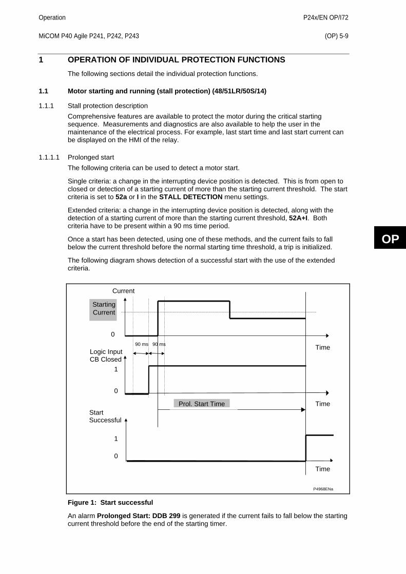
Operation
P24x/EN OP/I72 MiCOM P40 Agile P241, P242, P243 (OP) 5-9
OP
1 OPERATION OF INDIVIDUAL PROTECTION FUNCTIONS The following sections detail the individual protection functions.
1.1 Motor starting and running (stall protection) (48/51LR/50S/14)
1.1.1 Stall protection description Comprehensive features are available to protect the motor during the critical starting sequence. Measurements and diagnostics are also available to help the user in the maintenance of the electrical process. For example, last start time and last start current can be displayed on the HMI of the relay.
1.1.1.1 Prolonged start The following criteria can be used to detect a motor start.
Single criteria: a change in the interrupting device position is detected. This is from open to closed or detection of a starting current of more than the starting current threshold. The start criteria is set to 52a or I in the STALL DETECTION menu settings.
Extended criteria: a change in the interrupting device position is detected, along with the detection of a starting current of more than the starting current threshold, 52A+I. Both criteria have to be present within a 90 ms time period.
Once a start has been detected, using one of these methods, and the current fails to fall below the current threshold before the normal starting time threshold, a trip is initialized.
The following diagram shows detection of a successful start with the use of the extended criteria.
0
1
0
1
StartSuccessful
Current
90 ms Time90 ms
Time
Time
Logic InputCB Closed
0
Prol. Start Time
Starting Current
P4968ENa
Figure 1: Start successful
An alarm Prolonged Start: DDB 299 is generated if the current fails to fall below the starting current threshold before the end of the starting timer.
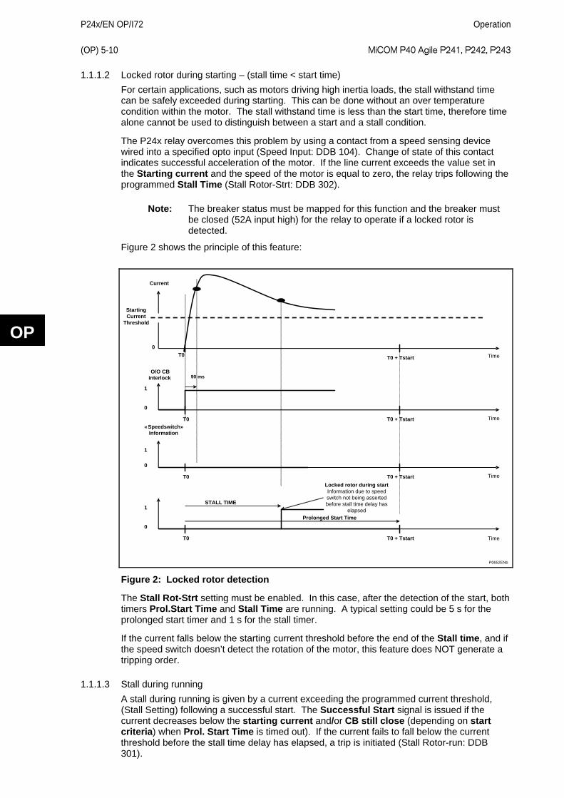
P24x/EN OP/I72
Operation (OP) 5-10 MiCOM P40 Agile P241, P242, P243
OP
1.1.1.2 Locked rotor during starting – (stall time < start time) For certain applications, such as motors driving high inertia loads, the stall withstand time can be safely exceeded during starting. This can be done without an over temperature condition within the motor. The stall withstand time is less than the start time, therefore time alone cannot be used to distinguish between a start and a stall condition.
The P24x relay overcomes this problem by using a contact from a speed sensing device wired into a specified opto input (Speed Input: DDB 104). Change of state of this contact indicates successful acceleration of the motor. If the line current exceeds the value set in the Starting current and the speed of the motor is equal to zero, the relay trips following the programmed Stall Time (Stall Rotor-Strt: DDB 302).
Note: The breaker status must be mapped for this function and the breaker must be closed (52A input high) for the relay to operate if a locked rotor is detected.
Figure 2 shows the principle of this feature:
90 ms
0
Starting Current
Threshold
Current
T0 T0 + Tstart
0
1
T0 T0 + Tstart
O/O CB interlock
0
1
T0 T0 + Tstart
« Speed switch» Information
Prolonged Start Time 0
1
T0 T0 + Tstart
Locked rotor during startInformation due to speed switch not being asserted before stall time delay has
elapsed
STALL TIME
Time
Time
Time
Time
P0652ENb
Figure 2: Locked rotor detection
The Stall Rot-Strt setting must be enabled. In this case, after the detection of the start, both timers Prol.Start Time and Stall Time are running. A typical setting could be 5 s for the prolonged start timer and 1 s for the stall timer.
If the current falls below the starting current threshold before the end of the Stall time, and if the speed switch doesn’t detect the rotation of the motor, this feature does NOT generate a tripping order.
1.1.1.3 Stall during running A stall during running is given by a current exceeding the programmed current threshold, (Stall Setting) following a successful start. The Successful Start signal is issued if the current decreases below the starting current and/or CB still close (depending on start criteria) when Prol. Start Time is timed out). If the current fails to fall below the current threshold before the stall time delay has elapsed, a trip is initiated (Stall Rotor-run: DDB 301).
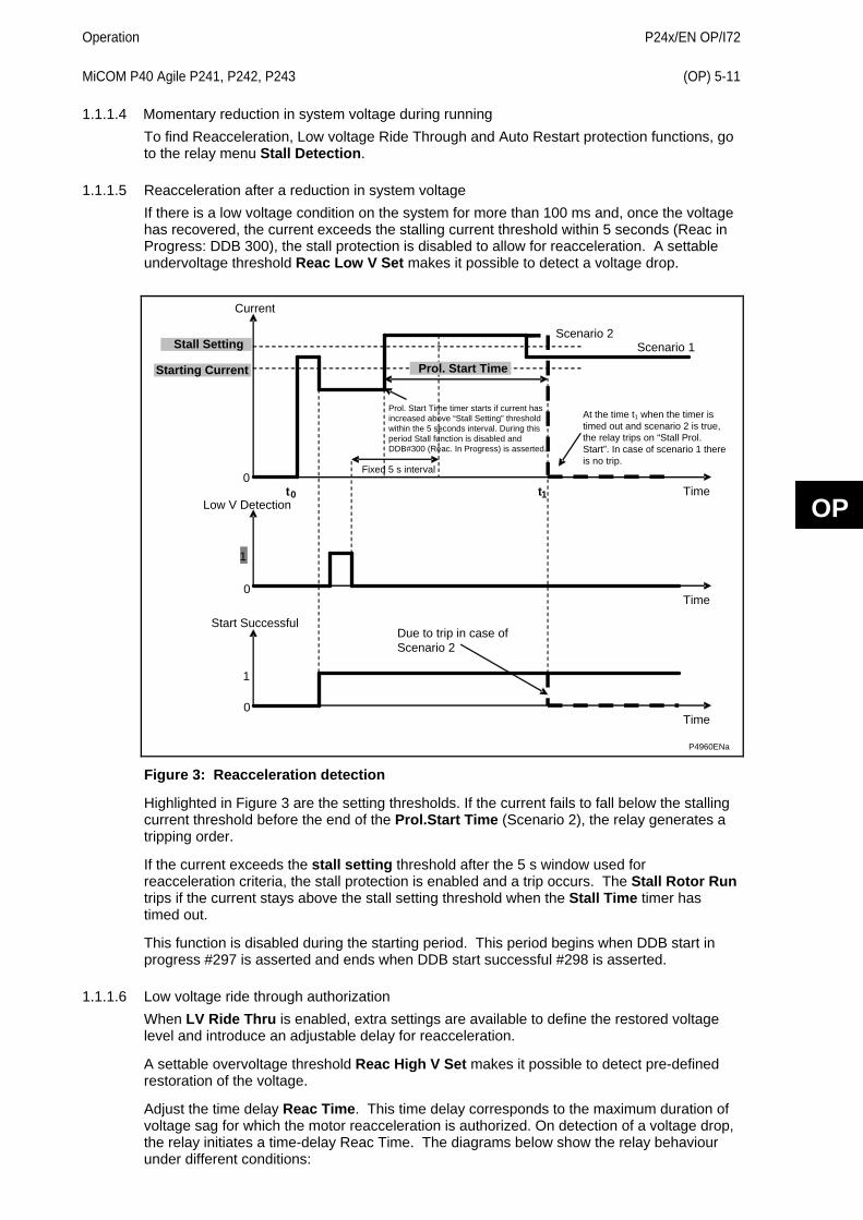
Operation
P24x/EN OP/I72 MiCOM P40 Agile P241, P242, P243 (OP) 5-11
OP
1.1.1.4 Momentary reduction in system voltage during running To find Reacceleration, Low voltage Ride Through and Auto Restart protection functions, go to the relay menu Stall Detection.
1.1.1.5 Reacceleration after a reduction in system voltage If there is a low voltage condition on the system for more than 100 ms and, once the voltage has recovered, the current exceeds the stalling current threshold within 5 seconds (Reac in Progress: DDB 300), the stall protection is disabled to allow for reacceleration. A settable undervoltage threshold Reac Low V Set makes it possible to detect a voltage drop.
Stall Setting Prol. Start Time
Fixed 5 s interval
Scenario 2
Due to trip in case of Scenario 2
Time
Time
Time
Current
Low V Detection
Start Successful
0
0
0
1
1
t0 t1
At the time t1 when the timer is timed out and scenario 2 is true, the relay trips on “Stall Prol. Start”. In case of scenario 1 there is no trip.
Prol. Start Time timer starts if current has increased above “Stall Setting” threshold within the 5 seconds interval. During this period Stall function is disabled and DDB#300 (Reac. In Progress) is asserted.
Scenario 1
Starting Current
P4960ENa
Figure 3: Reacceleration detection
Highlighted in Figure 3 are the setting thresholds. If the current fails to fall below the stalling current threshold before the end of the Prol.Start Time (Scenario 2), the relay generates a tripping order.
If the current exceeds the stall setting threshold after the 5 s window used for reacceleration criteria, the stall protection is enabled and a trip occurs. The Stall Rotor Run trips if the current stays above the stall setting threshold when the Stall Time timer has timed out.
This function is disabled during the starting period. This period begins when DDB start in progress #297 is asserted and ends when DDB start successful #298 is asserted.
1.1.1.6 Low voltage ride through authorization When LV Ride Thru is enabled, extra settings are available to define the restored voltage level and introduce an adjustable delay for reacceleration.
A settable overvoltage threshold Reac High V Set makes it possible to detect pre-defined restoration of the voltage.
Adjust the time delay Reac Time. This time delay corresponds to the maximum duration of voltage sag for which the motor reacceleration is authorized. On detection of a voltage drop, the relay initiates a time-delay Reac Time. The diagrams below show the relay behaviour under different conditions:
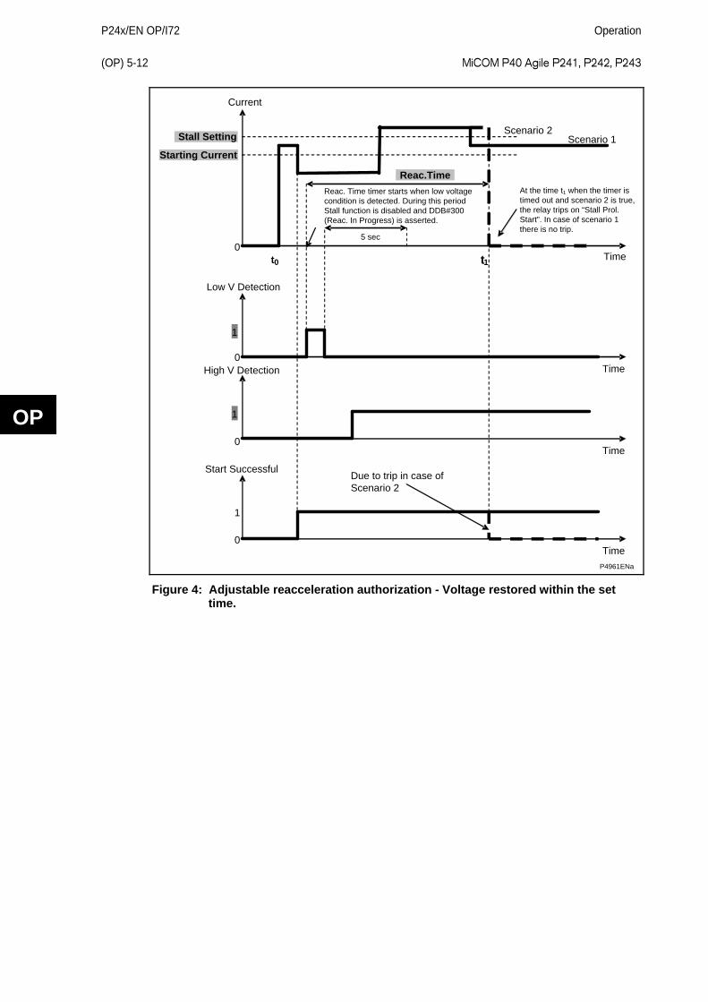
P24x/EN OP/I72
Operation (OP) 5-12 MiCOM P40 Agile P241, P242, P243
OP
Stall Setting Starting Current
Scenario 1 Scenario 2
Current
0
Due to trip in case of Scenario 2
Time
Time
Start Successful
0
Time
High V Detection
0
1
1
t0 t1
At the time t1 when the timer is timed out and scenario 2 is true, the relay trips on “Stall Prol. Start”. In case of scenario 1 there is no trip.
Time
Low V Detection
0
1
Reac.Time Reac. Time timer starts when low voltage condition is detected. During this period Stall function is disabled and DDB#300 (Reac. In Progress) is asserted.
5 sec
P4961ENa
Figure 4: Adjustable reacceleration authorization - Voltage restored within the set time.
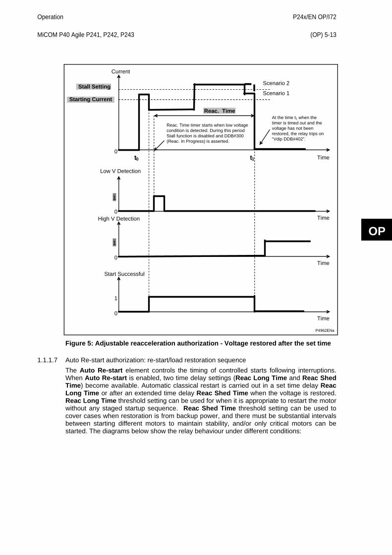
Operation
P24x/EN OP/I72 MiCOM P40 Agile P241, P242, P243 (OP) 5-13
OP
Stall Setting Starting Current
Scenario 1 Scenario 2
Current
0 Time
Time
Start Successful
0
Time
High V Detection
0
1
1
t0 t1
At the time t1 when the timer is timed out and the voltage has not been restored, the relay trips on “Vdip DDB#402”.
Time
Low V Detection
0
1
Reac. Time
Reac. Time timer starts when low voltage condition is detected. During this period Stall function is disabled and DDB#300 (Reac. In Progress) is asserted.
P4962ENa
Figure 5: Adjustable reacceleration authorization - Voltage restored after the set time
1.1.1.7 Auto Re-start authorization: re-start/load restoration sequence The Auto Re-start element controls the timing of controlled starts following interruptions. When Auto Re-start is enabled, two time delay settings (Reac Long Time and Reac Shed Time) become available. Automatic classical restart is carried out in a set time delay Reac Long Time or after an extended time delay Reac Shed Time when the voltage is restored. Reac Long Time threshold setting can be used for when it is appropriate to restart the motor without any staged startup sequence. Reac Shed Time threshold setting can be used to cover cases when restoration is from backup power, and there must be substantial intervals between starting different motors to maintain stability, and/or only critical motors can be started. The diagrams below show the relay behaviour under different conditions:
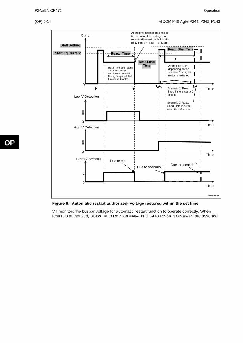
P24x/EN OP/I72
Operation (OP) 5-14 MiCOM P40 Agile P241, P242, P243
OP
Stall Setting Starting Current
Current
0
Due to trip
Time
Time
Start Successful
0
1
t0 t1
At the time t1 when the timer is timed out and the voltage has remained below Low V Set, the relay trips on “Stall Prol. Start”.
Time
Low V Detection
0
1
Reac. Time
Reac. Time timer starts when low voltage condition is detected. During this period Stall function is disabled.
Time
1
0
High V Detection
Reac.Long Time
Reac. Shed Time
t2 t3
At the time t2 or t3, depending on the scenario 1 or 2, the motor is restarted.
Scenario 2; Reac. Shed Time is set to other than 0 second.
Scenario 1; Reac. Shed Time is set to 0 second.
Due to scenario 1
Due to scenario 2
P4963ENa
Figure 6: Automatic restart authorized- voltage restored within the set time
VT monitors the busbar voltage for automatic restart function to operate correctly. When restart is authorized, DDBs “Auto Re-Start #404” and “Auto Re-Start OK #403” are asserted.
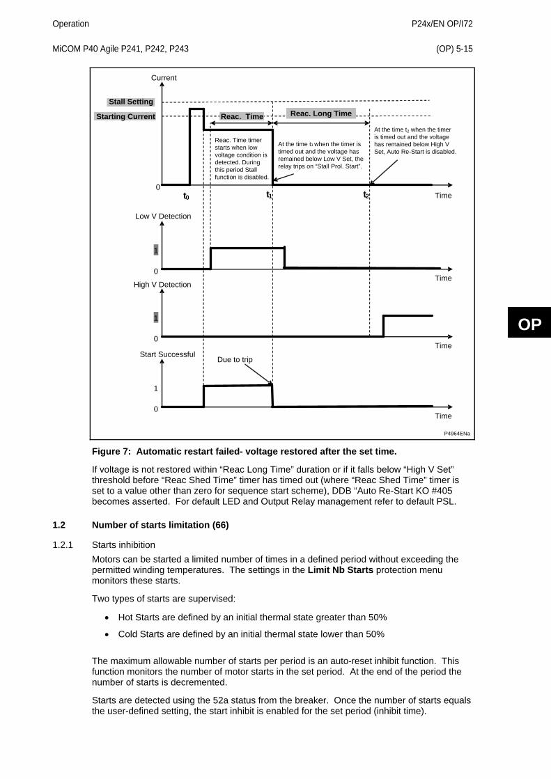
Operation
P24x/EN OP/I72 MiCOM P40 Agile P241, P242, P243 (OP) 5-15
OP
Stall Setting Starting Current
Current
0
Due to trip
Time
Time
Start Successful
0
1
t0 t1
At the time t1 when the timer is timed out and the voltage has remained below Low V Set, the relay trips on “Stall Prol. Start”.
Time
Low V Detection
0
1
Reac. Time
Reac. Time timer starts when low voltage condition is detected. During this period Stall function is disabled.
Time
1
0
High V Detection
Reac. Long Time
t2
At the time t2 when the timer is timed out and the voltage has remained below High V Set, Auto Re-Start is disabled.
P4964ENa
Figure 7: Automatic restart failed- voltage restored after the set time.
If voltage is not restored within “Reac Long Time” duration or if it falls below “High V Set” threshold before “Reac Shed Time” timer has timed out (where “Reac Shed Time” timer is set to a value other than zero for sequence start scheme), DDB “Auto Re-Start KO #405 becomes asserted. For default LED and Output Relay management refer to default PSL.
1.2 Number of starts limitation (66)
1.2.1 Starts inhibition Motors can be started a limited number of times in a defined period without exceeding the permitted winding temperatures. The settings in the Limit Nb Starts protection menu monitors these starts.
Two types of starts are supervised:
• Hot Starts are defined by an initial thermal state greater than 50%
• Cold Starts are defined by an initial thermal state lower than 50%
The maximum allowable number of starts per period is an auto-reset inhibit function. This function monitors the number of motor starts in the set period. At the end of the period the number of starts is decremented.
Starts are detected using the 52a status from the breaker. Once the number of starts equals the user-defined setting, the start inhibit is enabled for the set period (inhibit time).
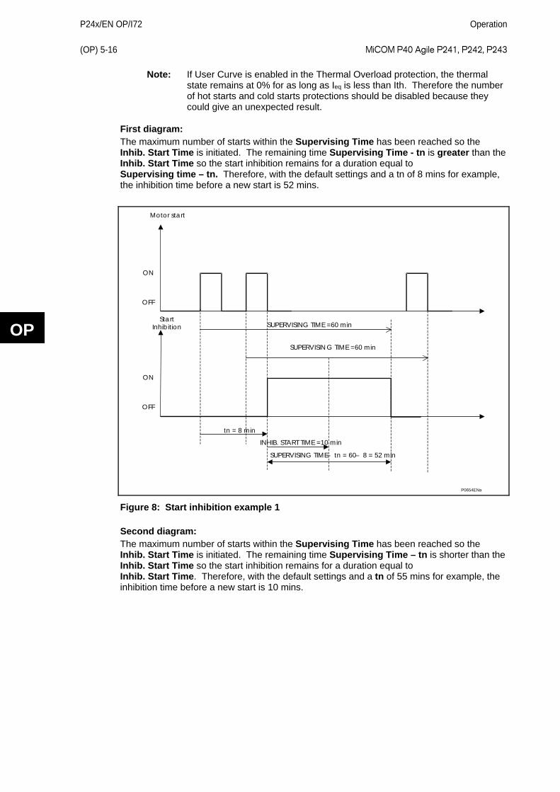
P24x/EN OP/I72
Operation (OP) 5-16 MiCOM P40 Agile P241, P242, P243
OP
Note: If User Curve is enabled in the Thermal Overload protection, the thermal state remains at 0% for as long as Ieq is less than Ith. Therefore the number of hot starts and cold starts protections should be disabled because they could give an unexpected result.
First diagram: The maximum number of starts within the Supervising Time has been reached so the Inhib. Start Time is initiated. The remaining time Supervising Time - tn is greater than the Inhib. Start Time so the start inhibition remains for a duration equal to Supervising time – tn. Therefore, with the default settings and a tn of 8 mins for example, the inhibition time before a new start is 52 mins.
ON
OFF
Start Inhibition SUPERVISING TIME =60 min
tn = 8 min INHIB. START TIME =10 min
SUPERVISING TIME – tn = 60 – 8 = 52 min
Motor start
ON
OFF
SUPERVISIN G TIME =60 min
P0654ENa
Figure 8: Start inhibition example 1
Second diagram: The maximum number of starts within the Supervising Time has been reached so the Inhib. Start Time is initiated. The remaining time Supervising Time – tn is shorter than the Inhib. Start Time so the start inhibition remains for a duration equal to Inhib. Start Time. Therefore, with the default settings and a tn of 55 mins for example, the inhibition time before a new start is 10 mins.
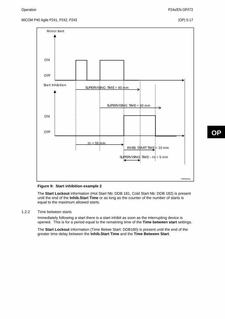
Operation
P24x/EN OP/I72 MiCOM P40 Agile P241, P242, P243 (OP) 5-17
OP
ON
OFF
Start Inhibition SUPERVISING TIME = 60 min
tn = 55 min INHIB. START TIME = 10 min
SUPERVISING TIME – tn = 5 min
SUPERVISING TIME = 60 min
ON
OFF
Motor start
P0655ENa
Figure 9: Start inhibition example 2
The Start Lockout information (Hot Start Nb: DDB 181, Cold Start Nb: DDB 182) is present until the end of the Inhib.Start Time or as long as the counter of the number of starts is equal to the maximum allowed starts.
1.2.2 Time between starts Immediately following a start there is a start inhibit as soon as the interrupting device is opened. This is for a period equal to the remaining time of the Time between start settings.
The Start Lockout information (Time Betwe Start: DDB180) is present until the end of the greater time delay between the Inhib.Start Time and the Time Between Start.
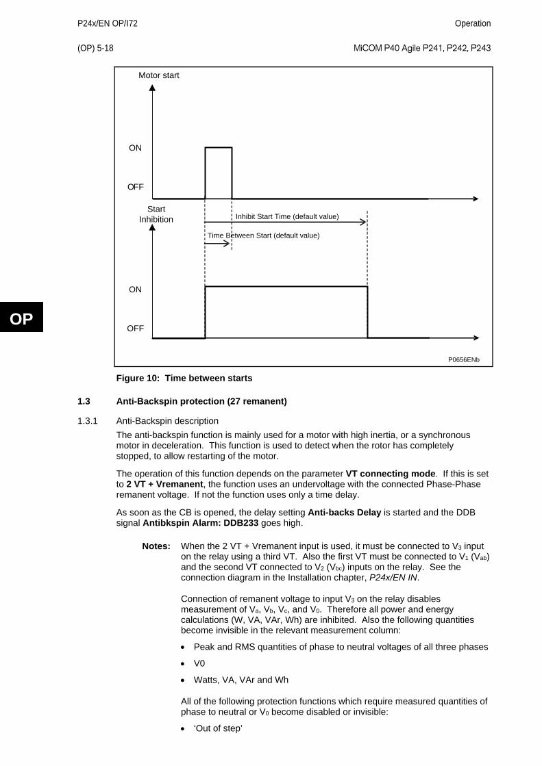
P24x/EN OP/I72
Operation (OP) 5-18 MiCOM P40 Agile P241, P242, P243
OP
ON
OFF
Start Inhibition
Time Between Start (default value)
Inhibit Start Time (default value)
ON
OFF
Motor start
P0656ENb
Figure 10: Time between starts
1.3 Anti-Backspin protection (27 remanent)
1.3.1 Anti-Backspin description The anti-backspin function is mainly used for a motor with high inertia, or a synchronous motor in deceleration. This function is used to detect when the rotor has completely stopped, to allow restarting of the motor.
The operation of this function depends on the parameter VT connecting mode. If this is set to 2 VT + Vremanent, the function uses an undervoltage with the connected Phase-Phase remanent voltage. If not the function uses only a time delay.
As soon as the CB is opened, the delay setting Anti-backs Delay is started and the DDB signal Antibkspin Alarm: DDB233 goes high.
Notes: When the 2 VT + Vremanent input is used, it must be connected to V3 input on the relay using a third VT. Also the first VT must be connected to V1 (Vab) and the second VT connected to V2 (Vbc) inputs on the relay. See the connection diagram in the Installation chapter, P24x/EN IN.
Connection of remanent voltage to input V3 on the relay disables measurement of Va, Vb, Vc, and V0. Therefore all power and energy calculations (W, VA, VAr, Wh) are inhibited. Also the following quantities become invisible in the relevant measurement column:
• Peak and RMS quantities of phase to neutral voltages of all three phases
• V0
• Watts, VA, VAr and Wh
All of the following protection functions which require measured quantities of phase to neutral or V0 become disabled or invisible:
• ‘Out of step’
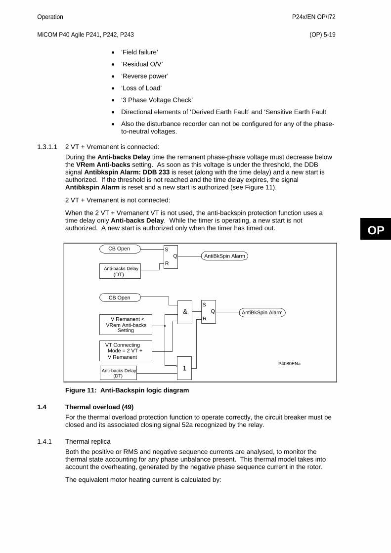
Operation
P24x/EN OP/I72 MiCOM P40 Agile P241, P242, P243 (OP) 5-19
OP
• ‘Field failure’
• ‘Residual O/V’
• ‘Reverse power’
• ‘Loss of Load’
• ‘3 Phase Voltage Check’
• Directional elements of ‘Derived Earth Fault’ and ‘Sensitive Earth Fault’
• Also the disturbance recorder can not be configured for any of the phase-to-neutral voltages.
1.3.1.1 2 VT + Vremanent is connected: During the Anti-backs Delay time the remanent phase-phase voltage must decrease below the VRem Anti-backs setting. As soon as this voltage is under the threshold, the DDB signal Antibkspin Alarm: DDB 233 is reset (along with the time delay) and a new start is authorized. If the threshold is not reached and the time delay expires, the signal Antibkspin Alarm is reset and a new start is authorized (see Figure 11).
2 VT + Vremanent is not connected:
When the 2 VT + Vremanent VT is not used, the anti-backspin protection function uses a time delay only Anti-backs Delay. While the timer is operating, a new start is not authorized. A new start is authorized only when the timer has timed out.
P4080ENa
CB Open
V Remanent <VRem Anti-backs
Setting
Mode = 2 VT +VT Connecting
V Remanent
&
CB Open AntiBkSpin Alarm
Anti-backs Delay(DT)
(DT)
S
RQ
S
RQ AntiBkSpin Alarm
1Anti-backs Delay
Figure 11: Anti-Backspin logic diagram
1.4 Thermal overload (49) For the thermal overload protection function to operate correctly, the circuit breaker must be closed and its associated closing signal 52a recognized by the relay.
1.4.1 Thermal replica Both the positive or RMS and negative sequence currents are analysed, to monitor the thermal state accounting for any phase unbalance present. This thermal model takes into account the overheating, generated by the negative phase sequence current in the rotor.
The equivalent motor heating current is calculated by:

P24x/EN OP/I72
Operation (OP) 5-20 MiCOM P40 Agile P241, P242, P243
OP
I eq = √(I12 + K I22)
Note: This equation is used in software version A4.x(09) and before
or
I eq = √(Irms2 + K I22)
Note: This equation is used in software version B1.0(20) or later
Where:
I1 = Positive sequence current
Irms : root mean square current
I2 : negative sequence current
K is a constant proportional to the thermal capacity of the motor
The equivalent motor heating current is calculated every 20 ms. The maximum value recorded is then used by the thermal algorithm.
1.4.2 Thermal trip A multiple time constant thermal replica is used to account for different operating conditions of the motor overload, starting or cooling conditions.
The equation used to calculate the trip time at 100% of thermal state is:
t = τ ln((k2 – A2)/(k2-1)) Where the value of τ (thermal time constant) depends on the current value absorbed by the motor:
Over load time constant τ = T1 if Ith < Ieq< = 2Ith
Start-up time constant τ = T2 if Ieq> 2Ith
Cooling time constant τ = Tr if interrupting device opened
Measured thermal load (or thermal capacity) k = Ieq / Ith
Ith is thermal setting
A is initial state of the machine in percentage of the thermal state
The initial state of the machine is included in the time to trip calculation algorithm. This is so that the operating time for a thermal trip is decreased if there is a hot motor start.
Some motors have extreme starting conditions such as a very long start time or a very high start current value. During start-up of these motors, the thermal curve is inhibited to avoid false trips.
Note: When the thermal state of the motor reaches 90%, this value is retained at 90% during the remaining period of the Prol. Start Time.
Comprehensive measurements and diagnostics can be accessed through the HMI. For example, the estimated time to the next thermal trip is calculated (see ‘MEASUREMENTS 3’ menu).
1.4.2.1 Compensation for ambient temperature by RTD To compensate for the ambient temperature variation, the thermal setting is corrected depending on the ambient temperature. The new value of the thermal capacity used becomes:
K′ = Ieq / (coef * Ith) Where the correction coefficient is calculated depending on the ambient temperature as shown below:
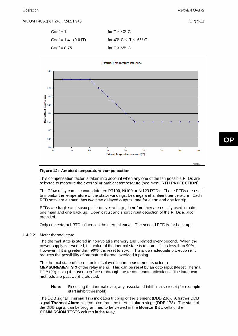
Operation
P24x/EN OP/I72 MiCOM P40 Agile P241, P242, P243 (OP) 5-21
OP
Coef = 1 for T < 40° C
Coef = 1.4 - (0.01T) for 40° C ≤ T ≤ 65° C
Coef = 0.75 for T > 65° C
Figure 12: Ambient temperature compensation
This compensation factor is taken into account when any one of the ten possible RTDs are selected to measure the external or ambient temperature (see menu RTD PROTECTION).
The P24x relay can accommodate ten PT100, Ni100 or Ni120 RTDs. These RTDs are used to monitor the temperature of the stator windings, bearings and ambient temperature. Each RTD software element has two time delayed outputs; one for alarm and one for trip.
RTDs are fragile and susceptible to over voltage, therefore they are usually used in pairs: one main and one back-up. Open circuit and short circuit detection of the RTDs is also provided.
Only one external RTD influences the thermal curve. The second RTD is for back-up.
1.4.2.2 Motor thermal state The thermal state is stored in non-volatile memory and updated every second. When the power supply is resumed, the value of the thermal state is restored if it is less than 90%. However, if it is greater than 90% it is reset to 90%. This allows adequate protection and reduces the possibility of premature thermal overload tripping.
The thermal state of the motor is displayed in the measurements column MEASUREMENTS 3 of the relay menu. This can be reset by an opto input (Reset Thermal: DDB109), using the user interface or through the remote communications. The latter two methods are password protected.
Note: Resetting the thermal state, any associated inhibits also reset (for example start inhibit threshold).
The DDB signal Thermal Trip indicates tripping of the element (DDB 236). A further DDB signal Thermal Alarm is generated from the thermal alarm stage (DDB 178). The state of the DDB signal can be programmed to be viewed in the Monitor Bit x cells of the COMMISSION TESTS column in the relay.
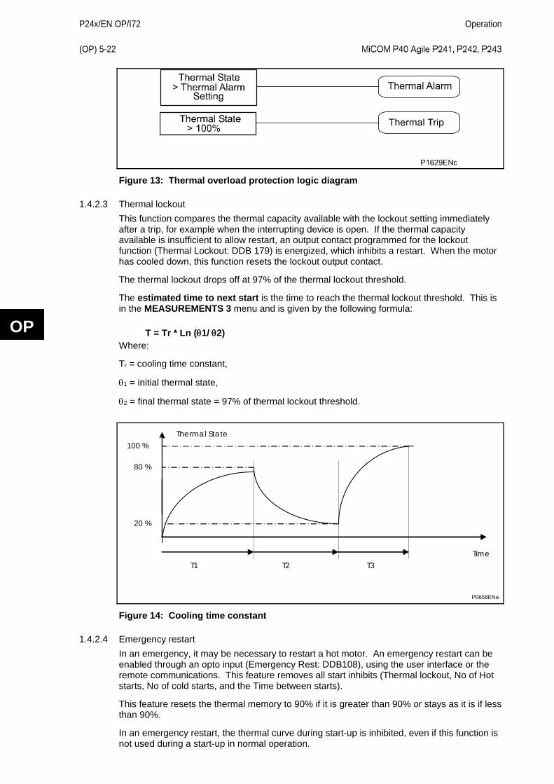
P24x/EN OP/I72
Operation (OP) 5-22 MiCOM P40 Agile P241, P242, P243
OP
Figure 13: Thermal overload protection logic diagram
1.4.2.3 Thermal lockout This function compares the thermal capacity available with the lockout setting immediately after a trip, for example when the interrupting device is open. If the thermal capacity available is insufficient to allow restart, an output contact programmed for the lockout function (Thermal Lockout: DDB 179) is energized, which inhibits a restart. When the motor has cooled down, this function resets the lockout output contact.
The thermal lockout drops off at 97% of the thermal lockout threshold.
The estimated time to next start is the time to reach the thermal lockout threshold. This is in the MEASUREMENTS 3 menu and is given by the following formula:
T = Tr * Ln (θ1/ θ2) Where:
Tr = cooling time constant,
θ1 = initial thermal state,
θ2 = final thermal state = 97% of thermal lockout threshold.
Thermal State
Time T1 T2 T3
20 %
80 %
100 %
P0658ENa
Figure 14: Cooling time constant
1.4.2.4 Emergency restart In an emergency, it may be necessary to restart a hot motor. An emergency restart can be enabled through an opto input (Emergency Rest: DDB108), using the user interface or the remote communications. This feature removes all start inhibits (Thermal lockout, No of Hot starts, No of cold starts, and the Time between starts).
This feature resets the thermal memory to 90% if it is greater than 90% or stays as it is if less than 90%.
In an emergency restart, the thermal curve during start-up is inhibited, even if this function is not used during a start-up in normal operation.
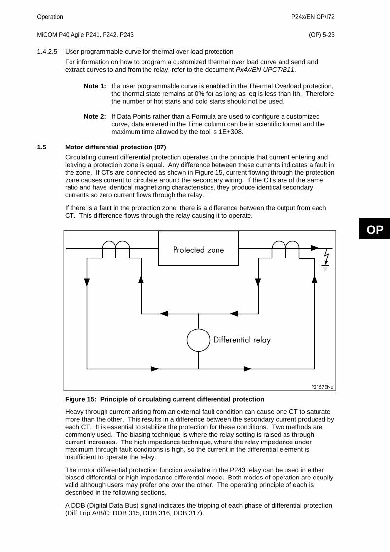
Operation
P24x/EN OP/I72 MiCOM P40 Agile P241, P242, P243 (OP) 5-23
OP
1.4.2.5 User programmable curve for thermal over load protection For information on how to program a customized thermal over load curve and send and extract curves to and from the relay, refer to the document Px4x/EN UPCT/B11.
Note 1: If a user programmable curve is enabled in the Thermal Overload protection, the thermal state remains at 0% for as long as Ieq is less than Ith. Therefore the number of hot starts and cold starts should not be used.
Note 2: If Data Points rather than a Formula are used to configure a customized curve, data entered in the Time column can be in scientific format and the maximum time allowed by the tool is 1E+308.
1.5 Motor differential protection (87) Circulating current differential protection operates on the principle that current entering and leaving a protection zone is equal. Any difference between these currents indicates a fault in the zone. If CTs are connected as shown in Figure 15, current flowing through the protection zone causes current to circulate around the secondary wiring. If the CTs are of the same ratio and have identical magnetizing characteristics, they produce identical secondary currents so zero current flows through the relay.
If there is a fault in the protection zone, there is a difference between the output from each CT. This difference flows through the relay causing it to operate.
Figure 15: Principle of circulating current differential protection
Heavy through current arising from an external fault condition can cause one CT to saturate more than the other. This results in a difference between the secondary current produced by each CT. It is essential to stabilize the protection for these conditions. Two methods are commonly used. The biasing technique is where the relay setting is raised as through current increases. The high impedance technique, where the relay impedance under maximum through fault conditions is high, so the current in the differential element is insufficient to operate the relay.
The motor differential protection function available in the P243 relay can be used in either biased differential or high impedance differential mode. Both modes of operation are equally valid although users may prefer one over the other. The operating principle of each is described in the following sections.
A DDB (Digital Data Bus) signal indicates the tripping of each phase of differential protection (Diff Trip A/B/C: DDB 315, DDB 316, DDB 317).
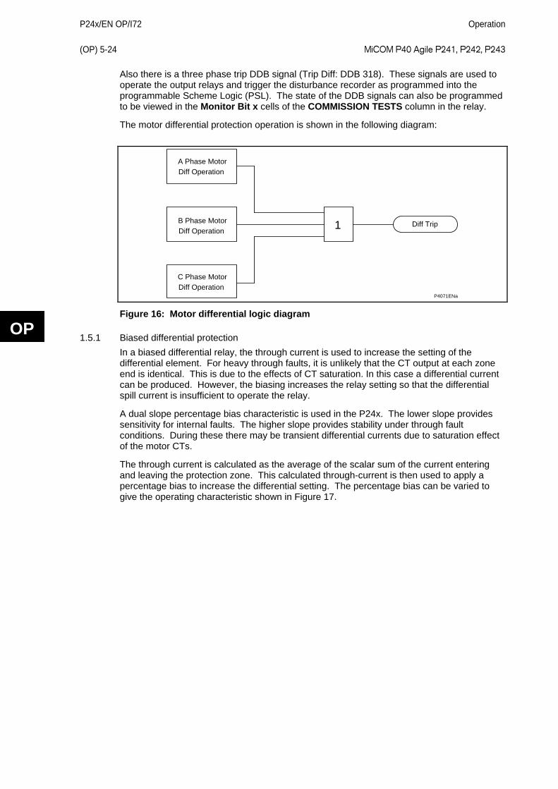
P24x/EN OP/I72
Operation (OP) 5-24 MiCOM P40 Agile P241, P242, P243
OP
Also there is a three phase trip DDB signal (Trip Diff: DDB 318). These signals are used to operate the output relays and trigger the disturbance recorder as programmed into the programmable Scheme Logic (PSL). The state of the DDB signals can also be programmed to be viewed in the Monitor Bit x cells of the COMMISSION TESTS column in the relay.
The motor differential protection operation is shown in the following diagram:
P4071ENa
Diff TripB Phase MotorDiff Operation
A Phase MotorDiff Operation
C Phase MotorDiff Operation
1
Figure 16: Motor differential logic diagram
1.5.1 Biased differential protection In a biased differential relay, the through current is used to increase the setting of the differential element. For heavy through faults, it is unlikely that the CT output at each zone end is identical. This is due to the effects of CT saturation. In this case a differential current can be produced. However, the biasing increases the relay setting so that the differential spill current is insufficient to operate the relay.
A dual slope percentage bias characteristic is used in the P24x. The lower slope provides sensitivity for internal faults. The higher slope provides stability under through fault conditions. During these there may be transient differential currents due to saturation effect of the motor CTs.
The through current is calculated as the average of the scalar sum of the current entering and leaving the protection zone. This calculated through-current is then used to apply a percentage bias to increase the differential setting. The percentage bias can be varied to give the operating characteristic shown in Figure 17.
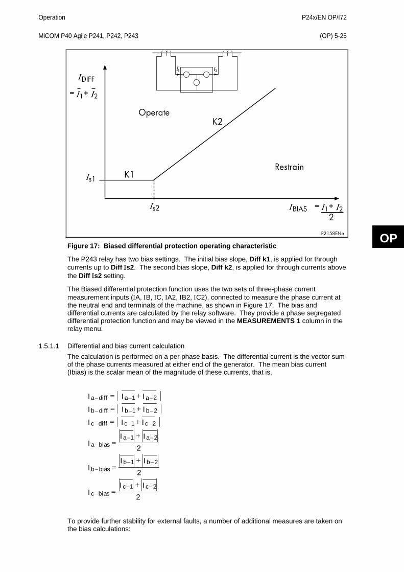
Operation
P24x/EN OP/I72 MiCOM P40 Agile P241, P242, P243 (OP) 5-25
OP
Figure 17: Biased differential protection operating characteristic
The P243 relay has two bias settings. The initial bias slope, Diff k1, is applied for through currents up to Diff Ιs2. The second bias slope, Diff k2, is applied for through currents above the Diff Ιs2 setting.
The Biased differential protection function uses the two sets of three-phase current measurement inputs (ΙA, ΙB, ΙC, ΙA2, ΙB2, ΙC2), connected to measure the phase current at the neutral end and terminals of the machine, as shown in Figure 17. The bias and differential currents are calculated by the relay software. They provide a phase segregated differential protection function and may be viewed in the MEASUREMENTS 1 column in the relay menu.
1.5.1.1 Differential and bias current calculation The calculation is performed on a per phase basis. The differential current is the vector sum of the phase currents measured at either end of the generator. The mean bias current (Ibias) is the scalar mean of the magnitude of these currents, that is,
a diff a aI I I− − −= +1 2
b diff b bI I I− − −= +1 2
c diff c cI I I− − −= +1 2
a bias
a aI
I I−
− −=
+1 2
2
b bias
b bI
I I−
− −=
+1 2
2
c bias
c cI
I I−
− −=
+1 2
2
To provide further stability for external faults, a number of additional measures are taken on the bias calculations:
P24x/EN OP/I72
Operation (OP) 5-26 MiCOM P40 Agile P241, P242, P243
OP
1.5.1.1.1 Delayed bias
The bias quantity used is the maximum of the bias quantities calculated in the last cycle. This maintains the bias level, providing stability while an external fault is cleared. This feature is implemented on a per phase basis. The algorithm is expressed as follows; the function is executed 4 times per cycle:
Ia-bias(n) = Maximum [Ia-bias(n), Ia-bias(n-1), ........., Ia-bias(n - 3)]
Ib-bias(n) = Maximum [Ib-bias(n), Ib-bias(n-1),........., Ib-bias(n - 3)]
Ic-bias(n) = Maximum [Ic-bias(n), Ic-bias(n-1), ........., Ic-bias(n - 3)]
1.5.1.1.2 Transient bias
If there is a sudden increase in the mean-bias measurement, an additional bias quantity is introduced into the bias calculation on a per phase basis. This bias quantity decays exponentially afterwards. The transient bias is reset to zero once the relay has tripped or if the mean bias quantity is below the Is1 setting. The transient bias is used to make the protection stable for external faults. It also allows for the time delay in CT saturation caused by small external fault currents and high X/R ratios. For single-end or double-end fed faults, the differential current is dominant and the transient bias has no effect.
The transient bias is removed after the relay has tripped to avoid the possibility of chattering. It is also removed when Ibias is less than Is1 to avoid the possibility of residual values due to the numerical effects.
1.5.1.1.3 Maximum bias
The bias quantity used per phase for the percentage bias characteristic is the maximum bias current calculated from all three phases,
I-bias-max = Maximum [Ia-bias, Ib-bias, Ic-bias]
1.5.1.1.4 Tripping criteria
The tripping criteria per phase are formulated as follows. The differential threshold changes according to the value of I-bias-max, as in the percentage bias characteristic.
Note: The transient bias is on a per phase basis and is not be affected by the K1 or K2 setting.
For I-bias-max <= Is2
Idiff > K1*I-bias-max + Transient_bias + Is1
For I-bias-max > Is2
Idiff > K2*I-bias-max + Transient Bias - Is2*(K2-K1) + Is1
A count strategy is used so the protection operates slower near the boundary of operation. This approach is used to stabilize the relay under some marginal transient conditions.
Operation
P24x/EN OP/I72 MiCOM P40 Agile P241, P242, P243 (OP) 5-27
OP
Figure 18: Relay connections for biased differential protection
1.5.2 High impedance differential protection The high impedance principle is best explained by considering a differential scheme where one CT is saturated for an external fault, as shown in Figure 19.
P24x/EN OP/I72
Operation (OP) 5-28 MiCOM P40 Agile P241, P242, P243
OP
Figure 19: Principle of high impedance differential protection
If the relay circuit is considered to be very high impedance, the secondary current produced by the healthy CT flows through the saturated CT. If the magnetizing impedance of the saturated CT is considered to be negligible, the maximum voltage across the relay circuit is equal to the secondary fault current multiplied by the connected impedance, (RL3 + RL4 + RCT2).
The relay can be made stable for this maximum applied voltage by increasing the overall impedance of the relay circuit, so the resulting current through the relay is less than its current setting. As the impedance of the relay input alone is relatively low, a series connected external resistor is required. The value of this resistor, RST, is calculated by the formula shown in Figure 19. An additional non-linear resistor (Metrosil) may be required to limit the peak secondary circuit voltage during internal fault conditions.
To ensure that the protection operates quickly during an internal fault, the CTs used to operate the protection must have a knee point voltage of at least 2 Vs.
The high impedance differential protection function uses the ΙA2, ΙB2, ΙC2 current inputs connected to measure the differential current in each phase, as shown in Figure 20.
Operation
P24x/EN OP/I72 MiCOM P40 Agile P241, P242, P243 (OP) 5-29
OP
Figure 20: Relay connections for high impedance differential protection
1.5.3 Self balance winding differential An alternative is to use self balance type differential protection arrangement, as shown in Figure 21, using the IA2, IB2, IC2 set of CTs
For this configuration, the relay must be set to High Impedance using the cell Diff Function in the Differential protection menu
Spill current can be kept to a minimum if the conductors are placed reasonably concentrically in the window of the core balance current transformers. With this low spill current and a reasonable independence of CT ratio to full load, a lower fault setting could be achieved compared to conventional high impedance circulating current differential schemes.
Disadvantages 1. Both ends of each phase winding need to pass through the CT. Therefore extra
cabling is needed on the neutral end.
2. To avoid long cabling, the position of CTs is restricted to the proximity of the machine output terminals. In this case the cable between the machine output terminals and controlling switchgear might not be included in the differential zone.
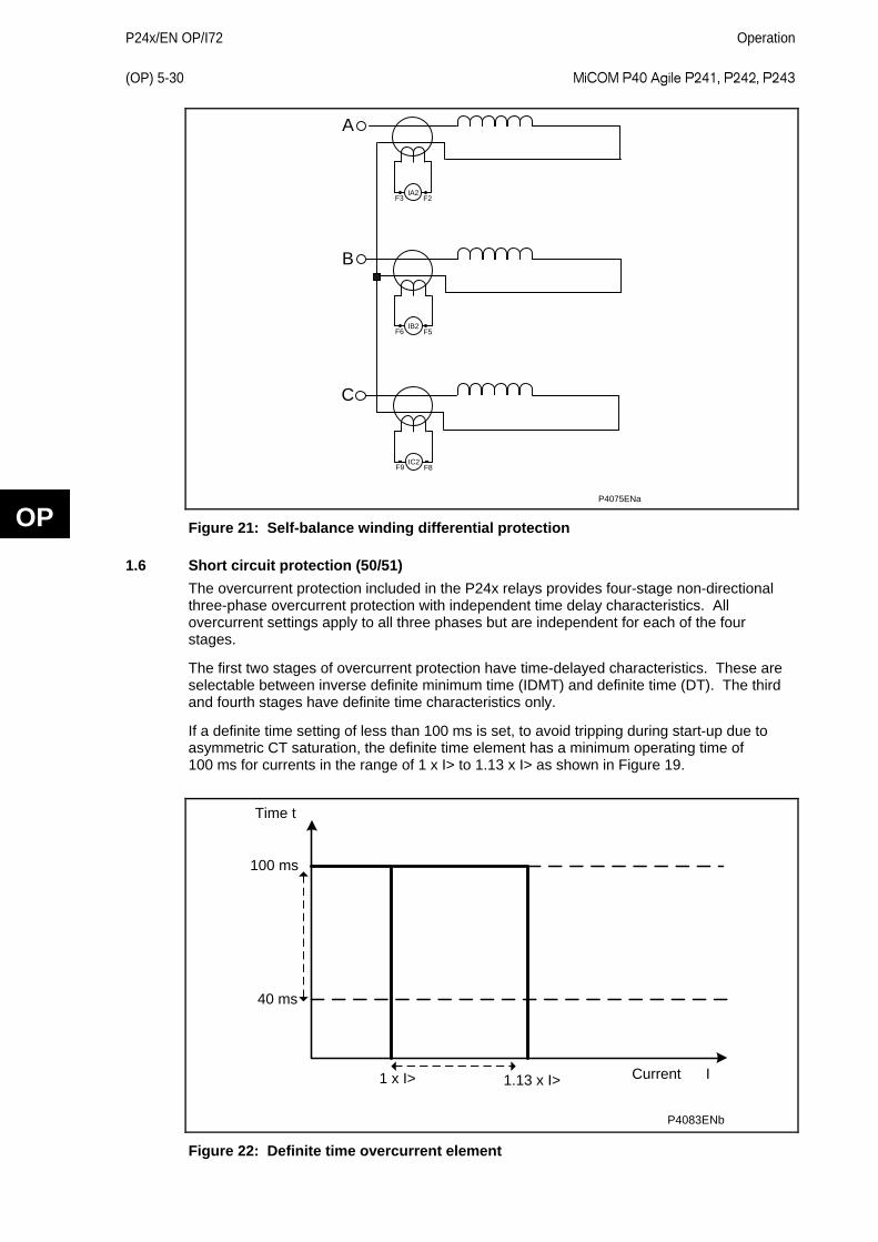
P24x/EN OP/I72
Operation (OP) 5-30 MiCOM P40 Agile P241, P242, P243
OP
A
B
C
IA2F3 F2
IB2F6 F5
IC2F9 F8
P4075ENa
Figure 21: Self-balance winding differential protection
1.6 Short circuit protection (50/51) The overcurrent protection included in the P24x relays provides four-stage non-directional three-phase overcurrent protection with independent time delay characteristics. All overcurrent settings apply to all three phases but are independent for each of the four stages.
The first two stages of overcurrent protection have time-delayed characteristics. These are selectable between inverse definite minimum time (IDMT) and definite time (DT). The third and fourth stages have definite time characteristics only.
If a definite time setting of less than 100 ms is set, to avoid tripping during start-up due to asymmetric CT saturation, the definite time element has a minimum operating time of 100 ms for currents in the range of 1 x I> to 1.13 x I> as shown in Figure 19.
P4083ENb
Time t
100 ms
1 x I> 1.13 x I> Current I
40 ms
Figure 22: Definite time overcurrent element
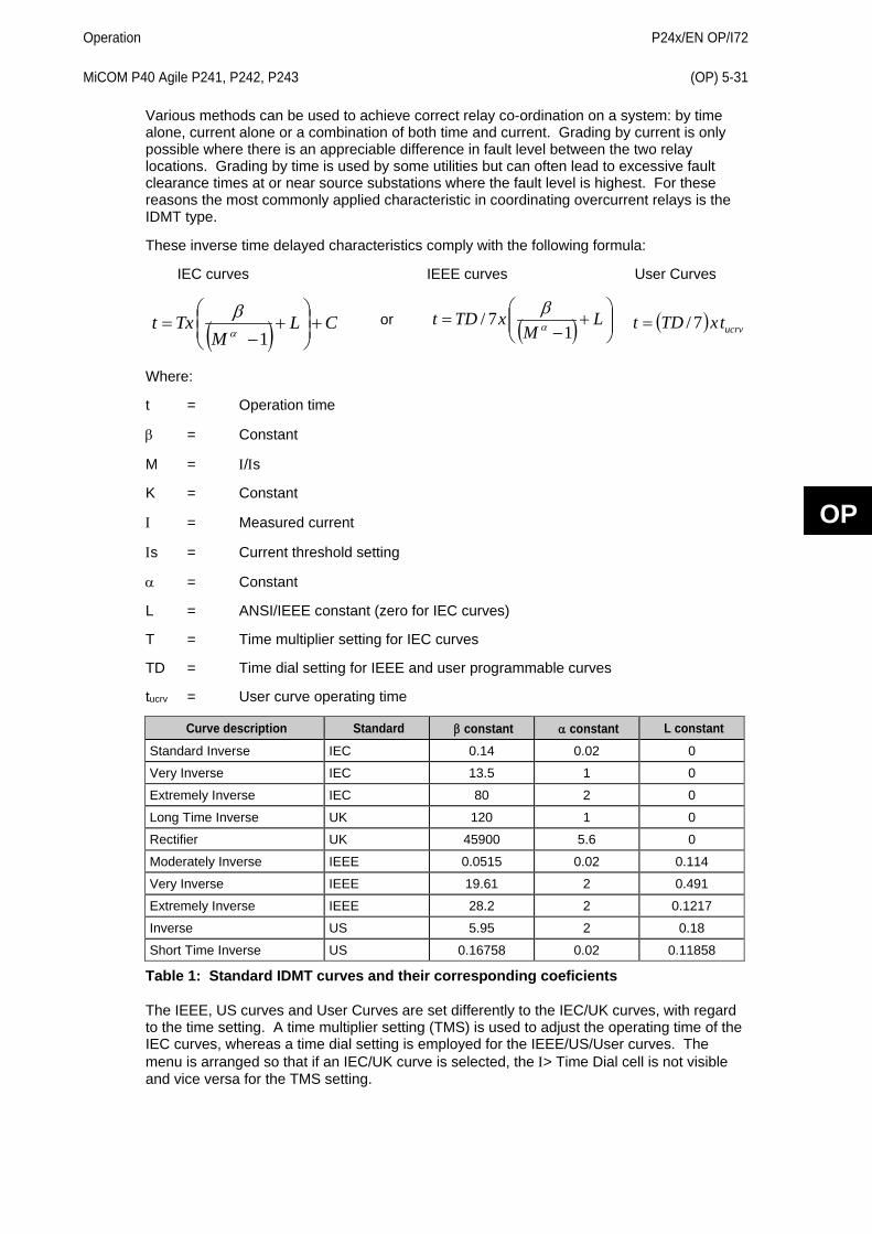
Operation
P24x/EN OP/I72 MiCOM P40 Agile P241, P242, P243 (OP) 5-31
OP
Various methods can be used to achieve correct relay co-ordination on a system: by time alone, current alone or a combination of both time and current. Grading by current is only possible where there is an appreciable difference in fault level between the two relay locations. Grading by time is used by some utilities but can often lead to excessive fault clearance times at or near source substations where the fault level is highest. For these reasons the most commonly applied characteristic in coordinating overcurrent relays is the IDMT type.
These inverse time delayed characteristics comply with the following formula:
IEC curves IEEE curves User Curves
( ) CLM
Txt +
+
−=
1α
β
or ( )
+
−= L
MxTDt
17/ α
β
( ) ucrvtxTDt 7/=
Where:
t = Operation time
β = Constant
M = Ι/Ιs
K = Constant
Ι = Measured current
Ιs = Current threshold setting
α = Constant
L = ANSI/IEEE constant (zero for IEC curves)
T = Time multiplier setting for IEC curves
TD = Time dial setting for IEEE and user programmable curves
tucrv = User curve operating time
Curve description Standard β constant α constant L constant Standard Inverse IEC 0.14 0.02 0
Very Inverse IEC 13.5 1 0
Extremely Inverse IEC 80 2 0
Long Time Inverse UK 120 1 0
Rectifier UK 45900 5.6 0
Moderately Inverse IEEE 0.0515 0.02 0.114
Very Inverse IEEE 19.61 2 0.491
Extremely Inverse IEEE 28.2 2 0.1217
Inverse US 5.95 2 0.18
Short Time Inverse US 0.16758 0.02 0.11858
Table 1: Standard IDMT curves and their corresponding coeficients
The IEEE, US curves and User Curves are set differently to the IEC/UK curves, with regard to the time setting. A time multiplier setting (TMS) is used to adjust the operating time of the IEC curves, whereas a time dial setting is employed for the IEEE/US/User curves. The menu is arranged so that if an IEC/UK curve is selected, the Ι> Time Dial cell is not visible and vice versa for the TMS setting.
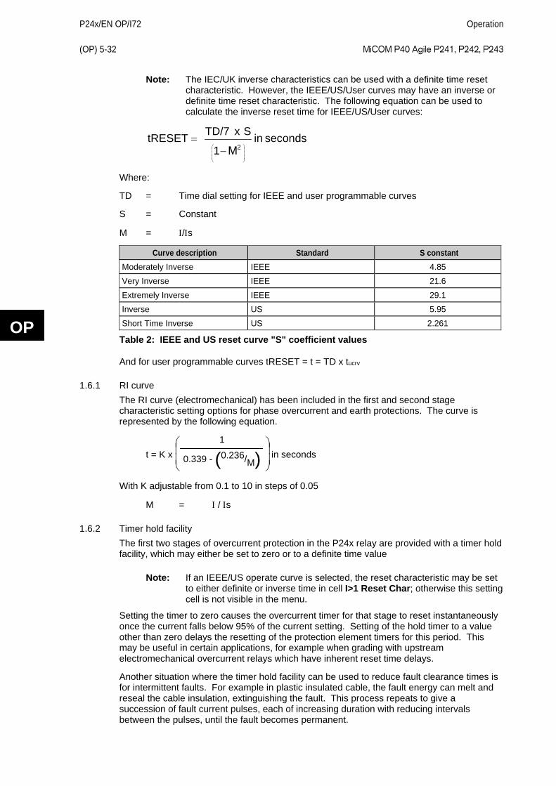
P24x/EN OP/I72
Operation (OP) 5-32 MiCOM P40 Agile P241, P242, P243
OP
Note: The IEC/UK inverse characteristics can be used with a definite time reset characteristic. However, the IEEE/US/User curves may have an inverse or definite time reset characteristic. The following equation can be used to calculate the inverse reset time for IEEE/US/User curves:
seconds in Μ1
SxTD/7tRESET2
−=
Where:
TD = Time dial setting for IEEE and user programmable curves
S = Constant
M = Ι/Ιs
Curve description Standard S constant Moderately Inverse IEEE 4.85
Very Inverse IEEE 21.6
Extremely Inverse IEEE 29.1
Inverse US 5.95
Short Time Inverse US 2.261
Table 2: IEEE and US reset curve "S" coefficient values
And for user programmable curves tRESET = t = TD x tucrv
1.6.1 RI curve The RI curve (electromechanical) has been included in the first and second stage characteristic setting options for phase overcurrent and earth protections. The curve is represented by the following equation.
t = K x
1
0.339 - ( )0.236/M in seconds
With K adjustable from 0.1 to 10 in steps of 0.05
M = Ι / Ιs
1.6.2 Timer hold facility The first two stages of overcurrent protection in the P24x relay are provided with a timer hold facility, which may either be set to zero or to a definite time value
Note: If an IEEE/US operate curve is selected, the reset characteristic may be set to either definite or inverse time in cell I>1 Reset Char; otherwise this setting cell is not visible in the menu.
Setting the timer to zero causes the overcurrent timer for that stage to reset instantaneously once the current falls below 95% of the current setting. Setting of the hold timer to a value other than zero delays the resetting of the protection element timers for this period. This may be useful in certain applications, for example when grading with upstream electromechanical overcurrent relays which have inherent reset time delays.
Another situation where the timer hold facility can be used to reduce fault clearance times is for intermittent faults. For example in plastic insulated cable, the fault energy can melt and reseal the cable insulation, extinguishing the fault. This process repeats to give a succession of fault current pulses, each of increasing duration with reducing intervals between the pulses, until the fault becomes permanent.
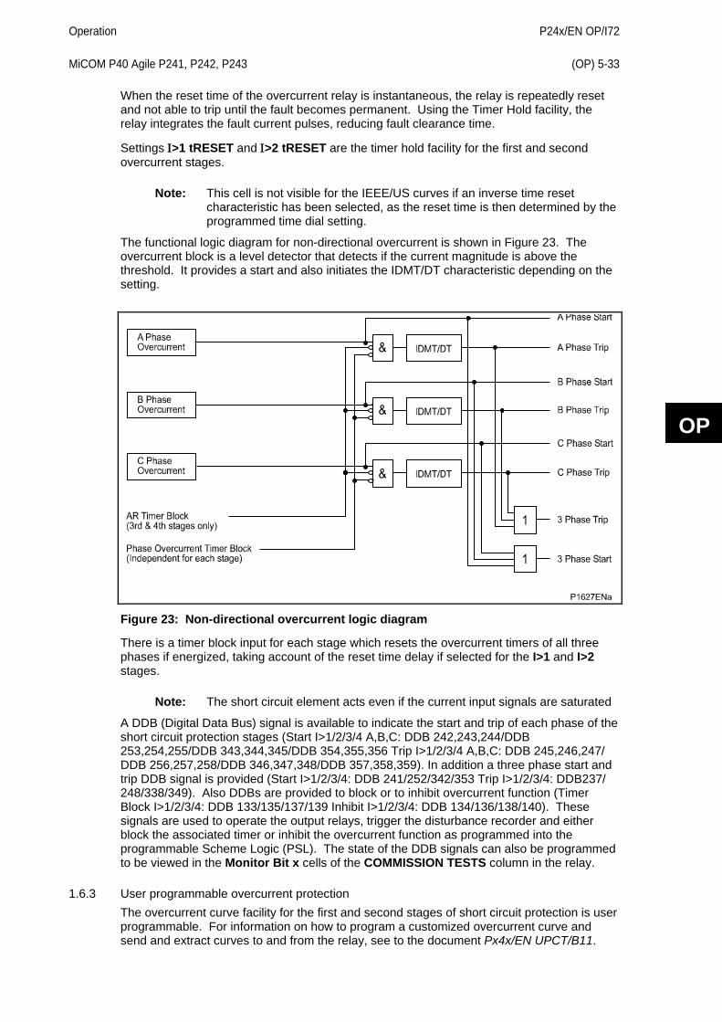
Operation
P24x/EN OP/I72 MiCOM P40 Agile P241, P242, P243 (OP) 5-33
OP
When the reset time of the overcurrent relay is instantaneous, the relay is repeatedly reset and not able to trip until the fault becomes permanent. Using the Timer Hold facility, the relay integrates the fault current pulses, reducing fault clearance time.
Settings Ι>1 tRESET and Ι>2 tRESET are the timer hold facility for the first and second overcurrent stages.
Note: This cell is not visible for the IEEE/US curves if an inverse time reset characteristic has been selected, as the reset time is then determined by the programmed time dial setting.
The functional logic diagram for non-directional overcurrent is shown in Figure 23. The overcurrent block is a level detector that detects if the current magnitude is above the threshold. It provides a start and also initiates the IDMT/DT characteristic depending on the setting.
Figure 23: Non-directional overcurrent logic diagram
There is a timer block input for each stage which resets the overcurrent timers of all three phases if energized, taking account of the reset time delay if selected for the I>1 and I>2 stages.
Note: The short circuit element acts even if the current input signals are saturated
A DDB (Digital Data Bus) signal is available to indicate the start and trip of each phase of the short circuit protection stages (Start I>1/2/3/4 A,B,C: DDB 242,243,244/DDB 253,254,255/DDB 343,344,345/DDB 354,355,356 Trip I>1/2/3/4 A,B,C: DDB 245,246,247/ DDB 256,257,258/DDB 346,347,348/DDB 357,358,359). In addition a three phase start and trip DDB signal is provided (Start I>1/2/3/4: DDB 241/252/342/353 Trip I>1/2/3/4: DDB237/ 248/338/349). Also DDBs are provided to block or to inhibit overcurrent function (Timer Block I>1/2/3/4: DDB 133/135/137/139 Inhibit I>1/2/3/4: DDB 134/136/138/140). These signals are used to operate the output relays, trigger the disturbance recorder and either block the associated timer or inhibit the overcurrent function as programmed into the programmable Scheme Logic (PSL). The state of the DDB signals can also be programmed to be viewed in the Monitor Bit x cells of the COMMISSION TESTS column in the relay.
1.6.3 User programmable overcurrent protection The overcurrent curve facility for the first and second stages of short circuit protection is user programmable. For information on how to program a customized overcurrent curve and send and extract curves to and from the relay, see to the document Px4x/EN UPCT/B11.
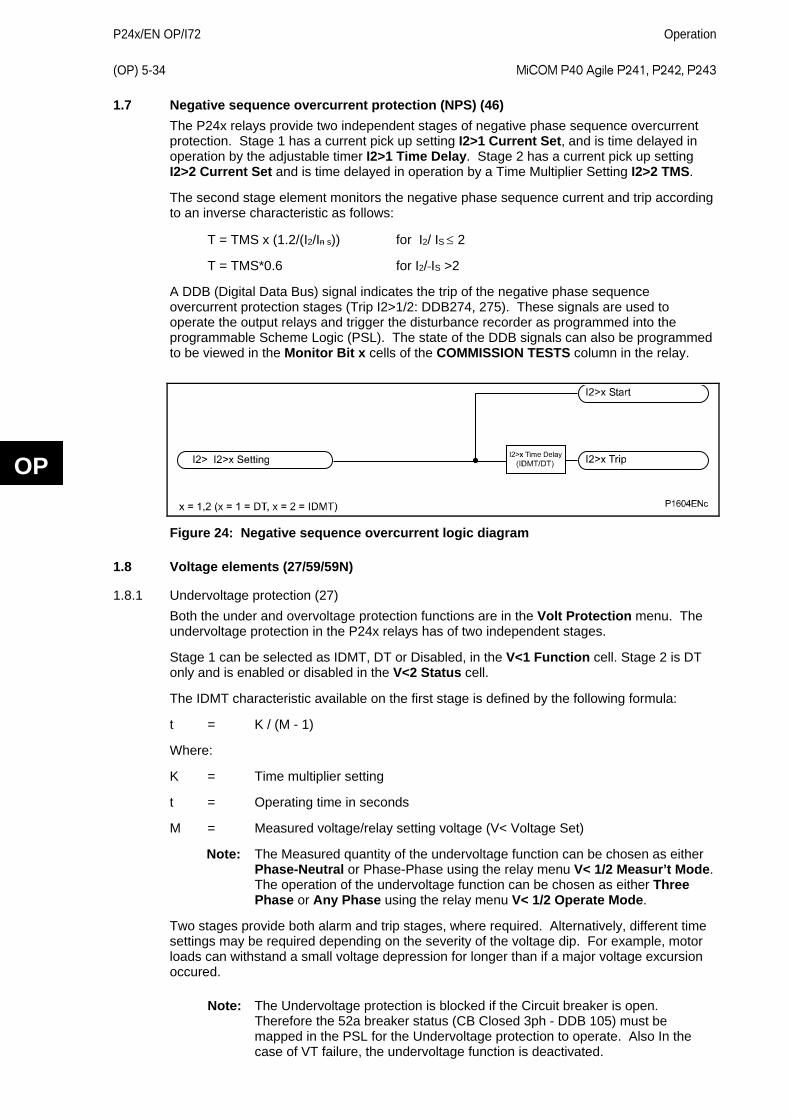
P24x/EN OP/I72
Operation (OP) 5-34 MiCOM P40 Agile P241, P242, P243
OP
1.7 Negative sequence overcurrent protection (NPS) (46) The P24x relays provide two independent stages of negative phase sequence overcurrent protection. Stage 1 has a current pick up setting I2>1 Current Set, and is time delayed in operation by the adjustable timer I2>1 Time Delay. Stage 2 has a current pick up setting I2>2 Current Set and is time delayed in operation by a Time Multiplier Setting I2>2 TMS.
The second stage element monitors the negative phase sequence current and trip according to an inverse characteristic as follows:
T = TMS x (1.2/(I2/In s)) for I2/ IS ≤ 2
T = TMS*0.6 for I2/ IS >2
A DDB (Digital Data Bus) signal indicates the trip of the negative phase sequence overcurrent protection stages (Trip I2>1/2: DDB274, 275). These signals are used to operate the output relays and trigger the disturbance recorder as programmed into the programmable Scheme Logic (PSL). The state of the DDB signals can also be programmed to be viewed in the Monitor Bit x cells of the COMMISSION TESTS column in the relay.
Figure 24: Negative sequence overcurrent logic diagram
1.8 Voltage elements (27/59/59N)
1.8.1 Undervoltage protection (27) Both the under and overvoltage protection functions are in the Volt Protection menu. The undervoltage protection in the P24x relays has of two independent stages.
Stage 1 can be selected as IDMT, DT or Disabled, in the V<1 Function cell. Stage 2 is DT only and is enabled or disabled in the V<2 Status cell.
The IDMT characteristic available on the first stage is defined by the following formula:
t = K / (M - 1)
Where:
K = Time multiplier setting
t = Operating time in seconds
M = Measured voltage/relay setting voltage (V< Voltage Set)
Note: The Measured quantity of the undervoltage function can be chosen as either Phase-Neutral or Phase-Phase using the relay menu V< 1/2 Measur’t Mode. The operation of the undervoltage function can be chosen as either Three Phase or Any Phase using the relay menu V< 1/2 Operate Mode.
Two stages provide both alarm and trip stages, where required. Alternatively, different time settings may be required depending on the severity of the voltage dip. For example, motor loads can withstand a small voltage depression for longer than if a major voltage excursion occured.
Note: The Undervoltage protection is blocked if the Circuit breaker is open. Therefore the 52a breaker status (CB Closed 3ph - DDB 105) must be mapped in the PSL for the Undervoltage protection to operate. Also In the case of VT failure, the undervoltage function is deactivated.
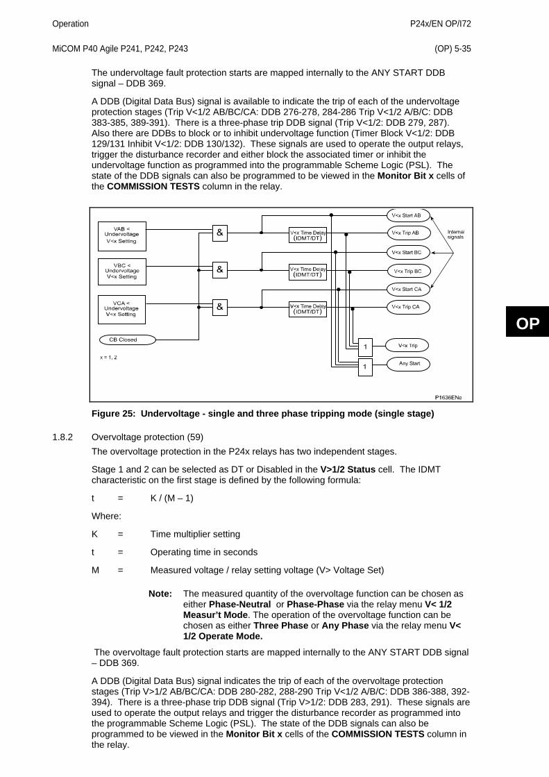
Operation
P24x/EN OP/I72 MiCOM P40 Agile P241, P242, P243 (OP) 5-35
OP
The undervoltage fault protection starts are mapped internally to the ANY START DDB signal – DDB 369.
A DDB (Digital Data Bus) signal is available to indicate the trip of each of the undervoltage protection stages (Trip V<1/2 AB/BC/CA: DDB 276-278, 284-286 Trip V<1/2 A/B/C: DDB 383-385, 389-391). There is a three-phase trip DDB signal (Trip V<1/2: DDB 279, 287). Also there are DDBs to block or to inhibit undervoltage function (Timer Block V<1/2: DDB 129/131 Inhibit V<1/2: DDB 130/132). These signals are used to operate the output relays, trigger the disturbance recorder and either block the associated timer or inhibit the undervoltage function as programmed into the programmable Scheme Logic (PSL). The state of the DDB signals can also be programmed to be viewed in the Monitor Bit x cells of the COMMISSION TESTS column in the relay.
Figure 25: Undervoltage - single and three phase tripping mode (single stage)
1.8.2 Overvoltage protection (59) The overvoltage protection in the P24x relays has two independent stages.
Stage 1 and 2 can be selected as DT or Disabled in the V>1/2 Status cell. The IDMT characteristic on the first stage is defined by the following formula:
t = K / (M – 1)
Where:
K = Time multiplier setting
t = Operating time in seconds
M = Measured voltage / relay setting voltage (V> Voltage Set)
Note: The measured quantity of the overvoltage function can be chosen as either Phase-Neutral or Phase-Phase via the relay menu V< 1/2 Measur’t Mode. The operation of the overvoltage function can be chosen as either Three Phase or Any Phase via the relay menu V< 1/2 Operate Mode.
The overvoltage fault protection starts are mapped internally to the ANY START DDB signal – DDB 369.
A DDB (Digital Data Bus) signal indicates the trip of each of the overvoltage protection stages (Trip V>1/2 AB/BC/CA: DDB 280-282, 288-290 Trip V<1/2 A/B/C: DDB 386-388, 392-394). There is a three-phase trip DDB signal (Trip V>1/2: DDB 283, 291). These signals are used to operate the output relays and trigger the disturbance recorder as programmed into the programmable Scheme Logic (PSL). The state of the DDB signals can also be programmed to be viewed in the Monitor Bit x cells of the COMMISSION TESTS column in the relay.
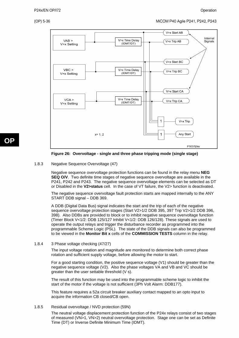
P24x/EN OP/I72
Operation (OP) 5-36 MiCOM P40 Agile P241, P242, P243
OP
Figure 26: Overvoltage - single and three phase tripping mode (single stage)
1.8.3 Negative Sequence Overvoltage (47)
Negative sequence overvoltage protection functions can be found in the relay menu NEG SEQ O/V. Two definite time stages of negative sequence overvoltage are available in the P241, P242 and P243. The negative sequence overvoltage elements can be selected as DT or Disabled in the V2>status cell. In the case of VT failure, the V2> function is deactivated.
The negative sequence overvoltage fault protection starts are mapped internally to the ANY START DDB signal – DDB 369.
A DDB (Digital Data Bus) signal indicates the start and the trip of each of the negative sequence overvoltage protection stages (Start V2>1/2 DDB 395, 397 Trip V2>1/2 DDB 396, 398). Also DDBs are provided to block or to inhibit negative sequence overvoltage function (Timer Block V<1/2: DDB 125/127 Inhibit V<1/2: DDB 126/128). These signals are used to operate the output relays and trigger the disturbance recorder as programmed into the programmable Scheme Logic (PSL). The state of the DDB signals can also be programmed to be viewed in the Monitor Bit x cells of the COMMISSION TESTS column in the relay.
1.8.4 3 Phase voltage checking (47/27) The input voltage rotation and magnitude are monitored to determine both correct phase rotation and sufficient supply voltage, before allowing the motor to start.
For a good starting condition, the positive sequence voltage (V1) should be greater than the negative sequence voltage (V2). Also the phase voltages VA and VB and VC should be greater than the user settable threshold (V s).
The result of this function may be used into the programmable scheme logic to inhibit the start of the motor if the voltage is not sufficient (3Ph Volt Alarm: DDB177).
This feature requires a 52a circuit breaker auxiliary contact mapped to an opto input to acquire the information CB closed/CB open.
1.8.5 Residual overvoltage / NVD protection (59N) The neutral voltage displacement protection function of the P24x relays consist of two stages of measured (VN>1, VN>2) neutral overvoltage protection. Stage one can be set as Definite Time (DT) or Inverse Definite Minimum Time (IDMT).
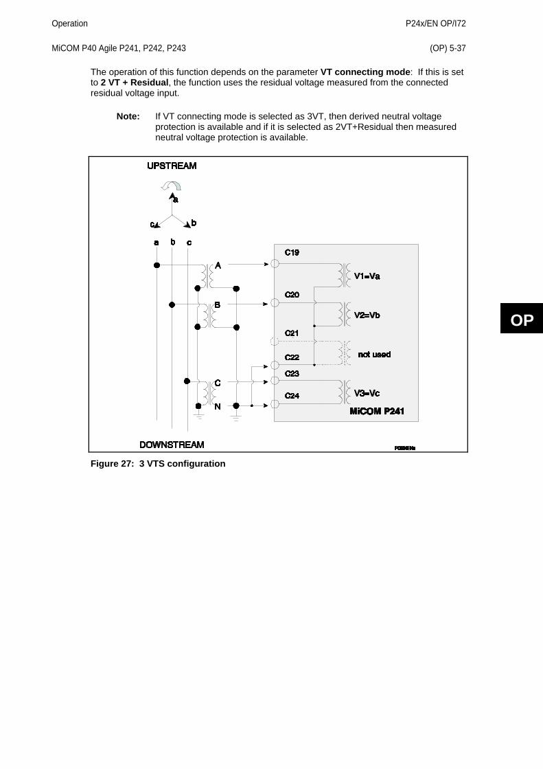
Operation
P24x/EN OP/I72 MiCOM P40 Agile P241, P242, P243 (OP) 5-37
OP
The operation of this function depends on the parameter VT connecting mode: If this is set to 2 VT + Residual, the function uses the residual voltage measured from the connected residual voltage input.
Note: If VT connecting mode is selected as 3VT, then derived neutral voltage protection is available and if it is selected as 2VT+Residual then measured neutral voltage protection is available.
Figure 27: 3 VTS configuration
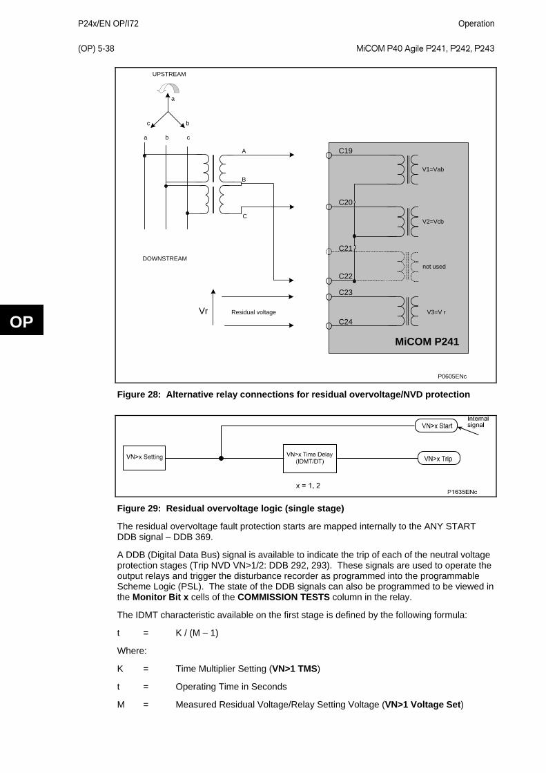
P24x/EN OP/I72
Operation (OP) 5-38 MiCOM P40 Agile P241, P242, P243
OP
P0605ENc
a b c
a
bc
UPSTREAM
A
B
C
C19
C20
C22
C21
C23
C24
V1=Vab
V2=Vcb
not used
V3=V r
MiCOM P241
Residual voltageVr
DOWNSTREAM
Figure 28: Alternative relay connections for residual overvoltage/NVD protection
Figure 29: Residual overvoltage logic (single stage)
The residual overvoltage fault protection starts are mapped internally to the ANY START DDB signal – DDB 369.
A DDB (Digital Data Bus) signal is available to indicate the trip of each of the neutral voltage protection stages (Trip NVD VN>1/2: DDB 292, 293). These signals are used to operate the output relays and trigger the disturbance recorder as programmed into the programmable Scheme Logic (PSL). The state of the DDB signals can also be programmed to be viewed in the Monitor Bit x cells of the COMMISSION TESTS column in the relay.
The IDMT characteristic available on the first stage is defined by the following formula:
t = K / (M – 1)
Where:
K = Time Multiplier Setting (VN>1 TMS)
t = Operating Time in Seconds
M = Measured Residual Voltage/Relay Setting Voltage (VN>1 Voltage Set)
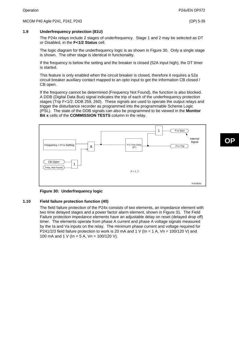
Operation
P24x/EN OP/I72 MiCOM P40 Agile P241, P242, P243 (OP) 5-39
OP
1.9 Underfrequency protection (81U) The P24x relays include 2 stages of underfrequency. Stage 1 and 2 may be selected as DT or Disabled, in the F<1/2 Status cell.
The logic diagram for the underfrequency logic is as shown in Figure 30. Only a single stage is shown. The other stage is identical in functionality.
If the frequency is below the setting and the breaker is closed (52A input high), the DT timer is started.
This feature is only enabled when the circuit breaker is closed, therefore it requires a 52a circuit breaker auxiliary contact mapped to an opto input to get the information CB closed / CB open.
If the frequency cannot be determined (Frequency Not Found), the function is also blocked. A DDB (Digital Data Bus) signal indicates the trip of each of the underfrequency protection stages (Trip F<1/2: DDB 259, 260). These signals are used to operate the output relays and trigger the disturbance recorder as programmed into the programmable Scheme Logic (PSL). The state of the DDB signals can also be programmed to be viewed in the Monitor Bit x cells of the COMMISSION TESTS column in the relay.
CB Open
InternalSignal
Frequency < F<x Setting
Freq. Not Found
F<x Time Delay(DT)
X = 1, 2
F<x Trip
F<x Start1
&
1
P1640ENc
Figure 30: Underfrequency logic
1.10 Field failure protection function (40) The field failure protection of the P24x consists of two elements, an impedance element with two time delayed stages and a power factor alarm element, shown in Figure 31. The Field Failure protection impedance elements have an adjustable delay on reset (delayed drop off) timer. The elements operate from phase A current and phase A voltage signals measured by the Ιa and Va inputs on the relay. The minimum phase current and voltage required for P241/2/3 field failure protection to work is 20 mA and 1 V (Ιn = 1 A, Vn = 100/120 V) and 100 mA and 1 V (Ιn = 5 A, Vn = 100/120 V).
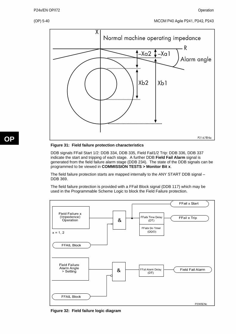
P24x/EN OP/I72
Operation (OP) 5-40 MiCOM P40 Agile P241, P242, P243
OP
Figure 31: Field failure protection characteristics
DDB signals FFail Start 1/2: DDB 334, DDB 335, Field Fail1/2 Trip: DDB 336, DDB 337 indicate the start and tripping of each stage. A further DDB Field Fail Alarm signal is generated from the field failure alarm stage (DDB 234). The state of the DDB signals can be programmed to be viewed in COMMISSION TESTS > Monitor Bit x.
The field failure protection starts are mapped internally to the ANY START DDB signal – DDB 369.
The field failure protection is provided with a FFail Block signal (DDB 117) which may be used in the Programmable Scheme Logic to block the Field Failure protection.
Figure 32: Field failure logic diagram
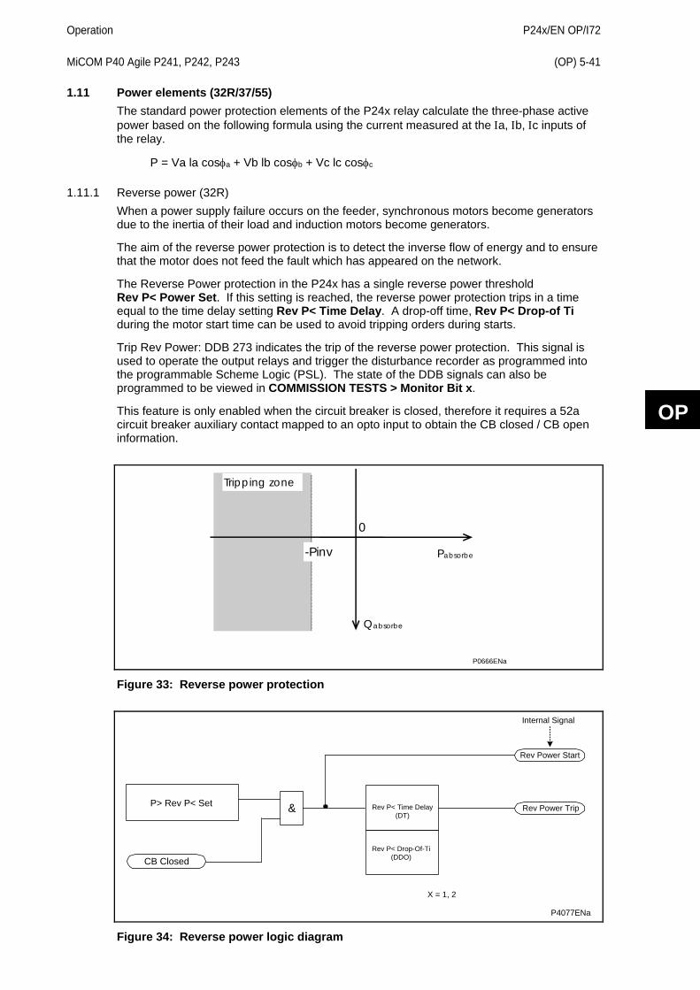
Operation
P24x/EN OP/I72 MiCOM P40 Agile P241, P242, P243 (OP) 5-41
OP
1.11 Power elements (32R/37/55) The standard power protection elements of the P24x relay calculate the three-phase active power based on the following formula using the current measured at the Ιa, Ιb, Ιc inputs of the relay.
P = Va la cosφa + Vb lb cosφb + Vc lc cosφc
1.11.1 Reverse power (32R) When a power supply failure occurs on the feeder, synchronous motors become generators due to the inertia of their load and induction motors become generators.
The aim of the reverse power protection is to detect the inverse flow of energy and to ensure that the motor does not feed the fault which has appeared on the network.
The Reverse Power protection in the P24x has a single reverse power threshold Rev P< Power Set. If this setting is reached, the reverse power protection trips in a time equal to the time delay setting Rev P< Time Delay. A drop-off time, Rev P< Drop-of Ti during the motor start time can be used to avoid tripping orders during starts.
Trip Rev Power: DDB 273 indicates the trip of the reverse power protection. This signal is used to operate the output relays and trigger the disturbance recorder as programmed into the programmable Scheme Logic (PSL). The state of the DDB signals can also be programmed to be viewed in COMMISSION TESTS > Monitor Bit x.
This feature is only enabled when the circuit breaker is closed, therefore it requires a 52a circuit breaker auxiliary contact mapped to an opto input to obtain the CB closed / CB open information.
Tripping zone
Qabsorbe
Pabsorbe
-Pinv
0
P0666ENa
Figure 33: Reverse power protection
CB Closed
P> Rev P< Set Rev P< Time Delay(DT)
X = 1, 2
Rev Power Trip&
Rev Power Start
Internal Signal
P4077ENa
Rev P< Drop-Of-Ti (DDO)
Figure 34: Reverse power logic diagram
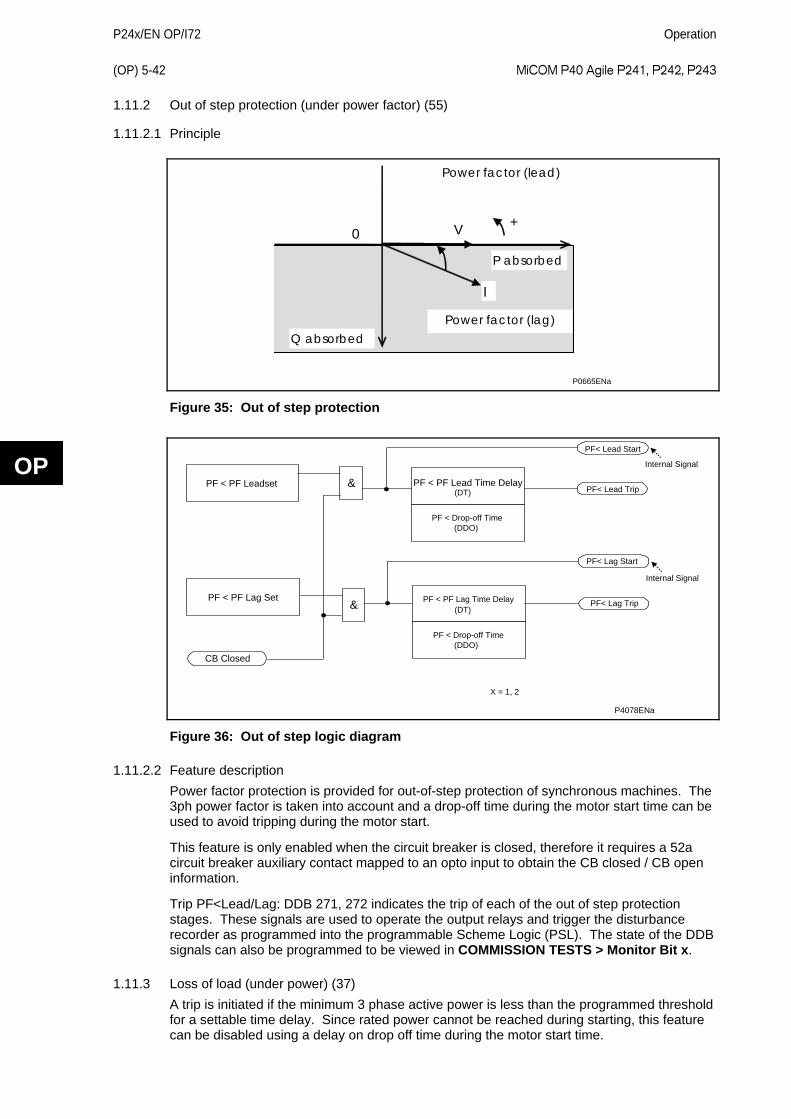
P24x/EN OP/I72
Operation (OP) 5-42 MiCOM P40 Agile P241, P242, P243
OP
1.11.2 Out of step protection (under power factor) (55)
1.11.2.1 Principle
Q absorbed
P absorbed
0
I
V +
Power factor (lag)
Power factor (lead)
P0665ENa
Figure 35: Out of step protection
CB Closed
PF < PF Lag Time Delay
X = 1, 2
PF< Lag Trip
PF< Lag Start
P4078ENa
PF < PF Lag Set& (DT)
Internal Signal
PF < Drop-off Time(DDO)
&(DT)
PF < PF Leadset
Internal Signal
PF < PF Lead Time DelayPF< Lead Trip
PF< Lead Start
PF < Drop-off Time(DDO)
Figure 36: Out of step logic diagram
1.11.2.2 Feature description Power factor protection is provided for out-of-step protection of synchronous machines. The 3ph power factor is taken into account and a drop-off time during the motor start time can be used to avoid tripping during the motor start.
This feature is only enabled when the circuit breaker is closed, therefore it requires a 52a circuit breaker auxiliary contact mapped to an opto input to obtain the CB closed / CB open information.
Trip PF<Lead/Lag: DDB 271, 272 indicates the trip of each of the out of step protection stages. These signals are used to operate the output relays and trigger the disturbance recorder as programmed into the programmable Scheme Logic (PSL). The state of the DDB signals can also be programmed to be viewed in COMMISSION TESTS > Monitor Bit x.
1.11.3 Loss of load (under power) (37) A trip is initiated if the minimum 3 phase active power is less than the programmed threshold for a settable time delay. Since rated power cannot be reached during starting, this feature can be disabled using a delay on drop off time during the motor start time.
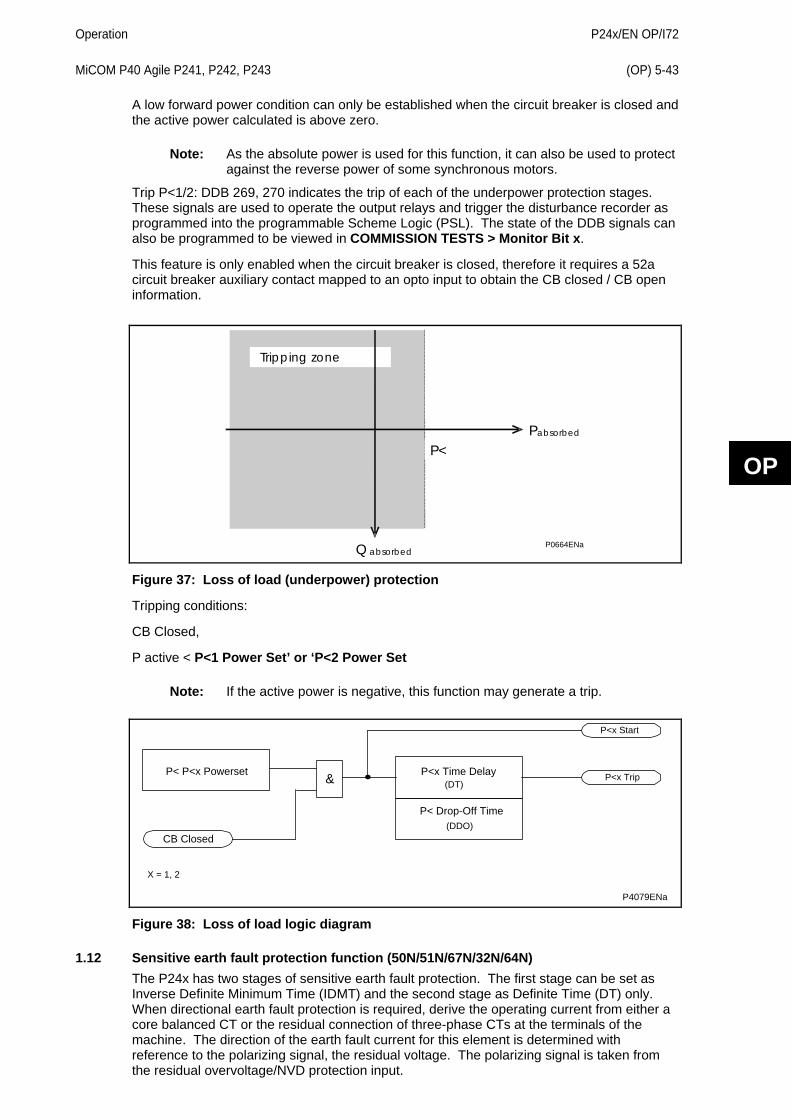
Operation
P24x/EN OP/I72 MiCOM P40 Agile P241, P242, P243 (OP) 5-43
OP
A low forward power condition can only be established when the circuit breaker is closed and the active power calculated is above zero.
Note: As the absolute power is used for this function, it can also be used to protect against the reverse power of some synchronous motors.
Trip P<1/2: DDB 269, 270 indicates the trip of each of the underpower protection stages. These signals are used to operate the output relays and trigger the disturbance recorder as programmed into the programmable Scheme Logic (PSL). The state of the DDB signals can also be programmed to be viewed in COMMISSION TESTS > Monitor Bit x.
This feature is only enabled when the circuit breaker is closed, therefore it requires a 52a circuit breaker auxiliary contact mapped to an opto input to obtain the CB closed / CB open information.
Tripping zone
Pabsorbed
P<
Qabsorbed P0664ENa
Figure 37: Loss of load (underpower) protection
Tripping conditions:
CB Closed,
P active < P<1 Power Set’ or ‘P<2 Power Set
Note: If the active power is negative, this function may generate a trip.
X = 1, 2
CB Closed
P<x Trip
P<x Start
P4079ENa
& (DT)P< P<x Powerset P<x Time Delay
P< Drop-Off Time (DDO)
Figure 38: Loss of load logic diagram
1.12 Sensitive earth fault protection function (50N/51N/67N/32N/64N) The P24x has two stages of sensitive earth fault protection. The first stage can be set as Inverse Definite Minimum Time (IDMT) and the second stage as Definite Time (DT) only. When directional earth fault protection is required, derive the operating current from either a core balanced CT or the residual connection of three-phase CTs at the terminals of the machine. The direction of the earth fault current for this element is determined with reference to the polarizing signal, the residual voltage. The polarizing signal is taken from the residual overvoltage/NVD protection input.
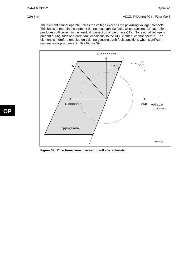
P24x/EN OP/I72
Operation (OP) 5-44 MiCOM P40 Agile P241, P242, P243
OP
The element cannot operate unless the voltage exceeds the polarizing voltage threshold. This helps to restrain the element during phase/phase faults when transient CT saturation produces spill current in the residual connection of the phase CTs. No residual voltage is present during such non-earth fault conditions so the DEF element cannot operate. The element is therefore enabled only during genuine earth fault conditions when significant residual voltage is present. See Figure 39.
α < 0
Tripping zone
IN
IN capacitive
IN resistive VNp
+
= voltage polarizing
P0660ENa
Figure 39: Directional sensitive earth fault characteristic
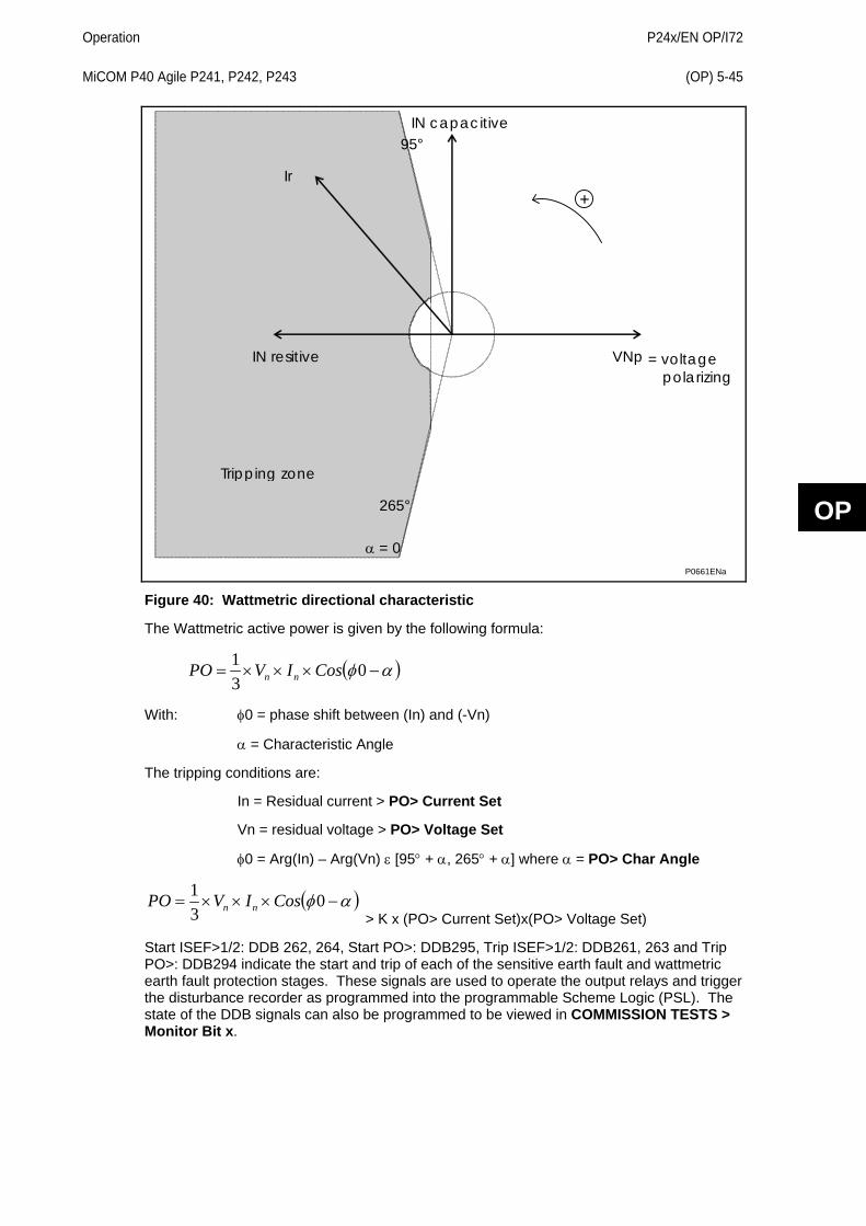
Operation
P24x/EN OP/I72 MiCOM P40 Agile P241, P242, P243 (OP) 5-45
OP
265°
95°
α = 0
Tripping zone
Ir
IN capacitive
IN resitive VNp = voltage polarizing
+
P0661ENa
Figure 40: Wattmetric directional characteristic
The Wattmetric active power is given by the following formula:
( )αφ −×××= 0
31 CosIVPO nn
With: φ0 = phase shift between (In) and (-Vn)
α = Characteristic Angle
The tripping conditions are:
In = Residual current > PO> Current Set
Vn = residual voltage > PO> Voltage Set
φ0 = Arg(In) – Arg(Vn) ε [95° + α, 265° + α] where α = PO> Char Angle
( )αφ −×××= 031 CosIVPO nn
> K x (PO> Current Set)x(PO> Voltage Set)
Start ISEF>1/2: DDB 262, 264, Start PO>: DDB295, Trip ISEF>1/2: DDB261, 263 and Trip PO>: DDB294 indicate the start and trip of each of the sensitive earth fault and wattmetric earth fault protection stages. These signals are used to operate the output relays and trigger the disturbance recorder as programmed into the programmable Scheme Logic (PSL). The state of the DDB signals can also be programmed to be viewed in COMMISSION TESTS > Monitor Bit x.
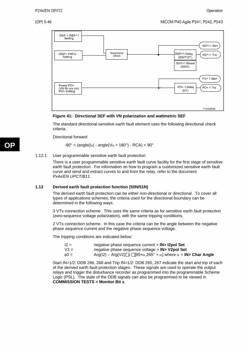
P24x/EN OP/I72
Operation (OP) 5-46 MiCOM P40 Agile P241, P242, P243
OP
Figure 41: Directional SEF with VN polarization and wattmetric SEF
The standard directional sensitive earth fault element uses the following directional check criteria.
Directional forward
-90° < (angle(IN) - angle(VN + 180°) - RCA) < 90°
1.12.1 User programmable sensitive earth fault protection There is a user programmable sensitive earth fault curve facility for the first stage of sensitive earth fault protection. For information on how to program a customized sensitive earth fault curve and send and extract curves to and from the relay, refer to the document Px4x/EN UPCT/B11.
1.13 Derived earth fault protection function (50N/51N) The derived earth fault protection can be either non-directional or directional. To cover all types of applications schemes, the criteria used for the directional boundary can be determined in the following ways.
3 VTs connection scheme. This uses the same criteria as for sensitive earth fault protection (zero-sequence voltage polarization), with the same tripping conditions,
2 VTs connection scheme. In this case the criteria can be the angle between the negative phase sequence current and the negative phase sequence voltage.
The tripping conditions are indicated below:
I2 = negative phase sequence current > IN> I2pol Set V2 = negative phase sequence voltage > IN> V2pol Set φ0 = Arg(I2) – Arg(V2)∈[95+α,265° + α] where α = IN> Char Angle
Start IN>1/2: DDB 266, 268 and Trip IN>1/2: DDB 265, 267 indicate the start and trip of each of the derived earth fault protection stages. These signals are used to operate the output relays and trigger the disturbance recorder as programmed into the programmable Scheme Logic (PSL). The state of the DDB signals can also be programmed to be viewed in COMMISSION TESTS > Monitor Bit x.
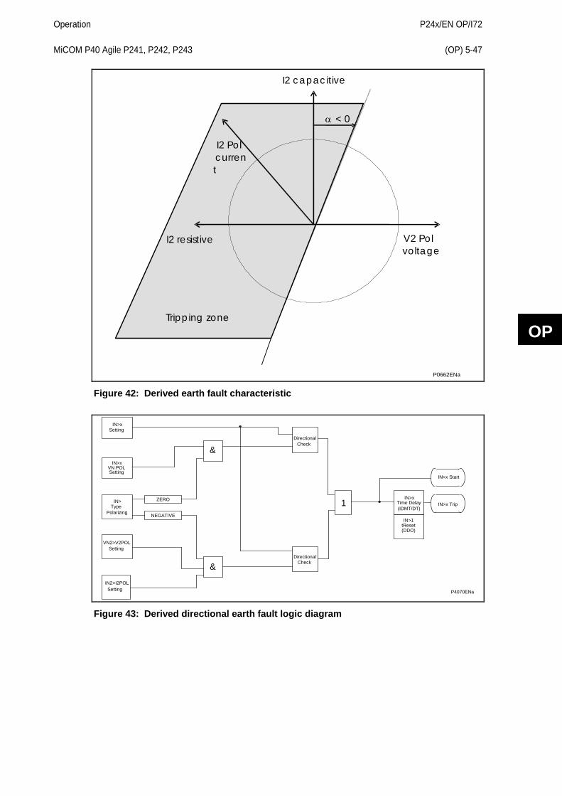
Operation
P24x/EN OP/I72 MiCOM P40 Agile P241, P242, P243 (OP) 5-47
OP
α < 0
Tripping zone
I2 Pol current
I2 capacitive
I2 resistive V2 Pol voltage
P0662ENa
Figure 42: Derived earth fault characteristic
IN>xSetting
IN>xVN POLSetting
IN> Type
Polarizing
VN2>V2POL Setting
IN2>I2POL Setting
ZERO
NEGATIVE
&
&Directional
Check
DirectionalCheck
1IN>x
Time Delay(IDMT/DT)
IN>x Start
P4070ENa
IN>x Trip
IN>1tReset(DDO)
Figure 43: Derived directional earth fault logic diagram
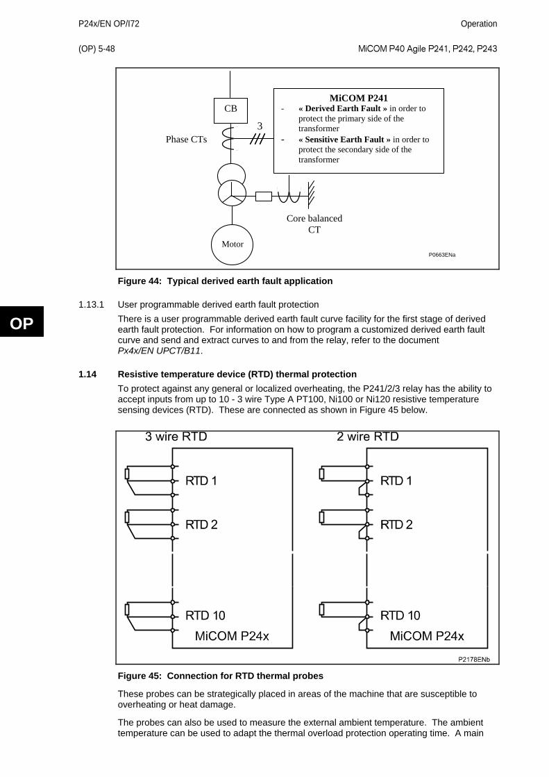
P24x/EN OP/I72
Operation (OP) 5-48 MiCOM P40 Agile P241, P242, P243
OP
CB
Motor
MiCOM P241 - « Derived Earth Fault » in order to
protect the primary side of the transformer
- « Sensitive Earth Fault » in order to protect the secondary side of the transformer
Core balanced CT
3 Phase CTs
P0663ENa
Figure 44: Typical derived earth fault application
1.13.1 User programmable derived earth fault protection There is a user programmable derived earth fault curve facility for the first stage of derived earth fault protection. For information on how to program a customized derived earth fault curve and send and extract curves to and from the relay, refer to the document Px4x/EN UPCT/B11.
1.14 Resistive temperature device (RTD) thermal protection To protect against any general or localized overheating, the P241/2/3 relay has the ability to accept inputs from up to 10 - 3 wire Type A PT100, Ni100 or Ni120 resistive temperature sensing devices (RTD). These are connected as shown in Figure 45 below.
Figure 45: Connection for RTD thermal probes
These probes can be strategically placed in areas of the machine that are susceptible to overheating or heat damage.
The probes can also be used to measure the external ambient temperature. The ambient temperature can be used to adapt the thermal overload protection operating time. A main
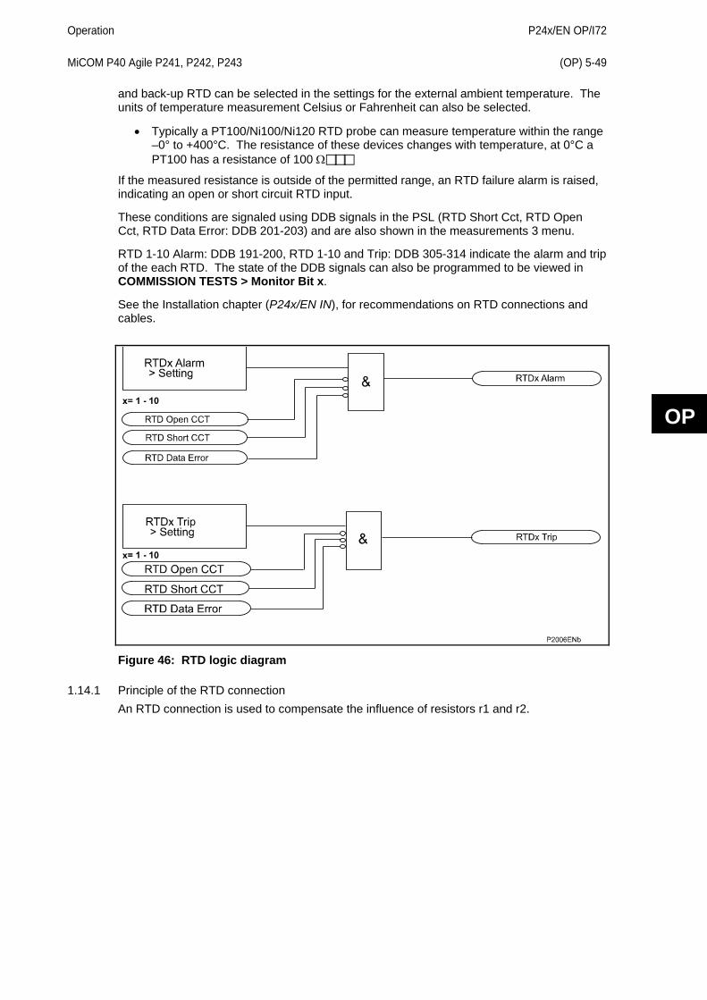
Operation
P24x/EN OP/I72 MiCOM P40 Agile P241, P242, P243 (OP) 5-49
OP
and back-up RTD can be selected in the settings for the external ambient temperature. The units of temperature measurement Celsius or Fahrenheit can also be selected.
• Typically a PT100/Ni100/Ni120 RTD probe can measure temperature within the range –0° to +400°C. The resistance of these devices changes with temperature, at 0°C a PT100 has a resistance of 100 Ω
If the measured resistance is outside of the permitted range, an RTD failure alarm is raised, indicating an open or short circuit RTD input.
These conditions are signaled using DDB signals in the PSL (RTD Short Cct, RTD Open Cct, RTD Data Error: DDB 201-203) and are also shown in the measurements 3 menu.
RTD 1-10 Alarm: DDB 191-200, RTD 1-10 and Trip: DDB 305-314 indicate the alarm and trip of the each RTD. The state of the DDB signals can also be programmed to be viewed in COMMISSION TESTS > Monitor Bit x.
See the Installation chapter (P24x/EN IN), for recommendations on RTD connections and cables.
Figure 46: RTD logic diagram
1.14.1 Principle of the RTD connection An RTD connection is used to compensate the influence of resistors r1 and r2.
P24x/EN OP/I72
Operation (OP) 5-50 MiCOM P40 Agile P241, P242, P243
OP
P4969ENa
Figure 47: RTD connection
The MICOM P241 injects a constant current from connections1 and 2, therefore i1 = i2
V13 = r1 * I1 + Rrtd * I1 - r3 * (I1 + I2),
V23 = r2 * I2 - r3 * (I1 + I2),
V13 - U23 = r1 * I1 + Rrtd * I1 - r3 * (I1 + I2) - r2 * I2 + r3 * (I1 + I2)
Assuming the three cables have the same length and are of the same material, resisitors r1, r2 and r3 are the same.
V13 - V23 = Rrtd * I1 = Voltage at the RTD terminals.
1.15 Circuit breaker failure protection (50BF) The circuit breaker failure protection has two timers, CB Fail 1 Timer and CB Fail 2 Timer, allowing configuration for the following situations.
• Simple CBF, where only CB Fail 1 Timer is enabled. For any protection trip the CB Fail 1 Timer is started and is normally reset when the circuit breaker opens to isolate the fault. If breaker opening is not detected, CB Fail 1 Timer times out and closes an output contact assigned to breaker fail (Trip CBF1: DDB 319, using PSL). This contact is used to backtrip upstream switchgear, generally tripping all infeeds connected to the same busbar section.
• A retripping scheme, plus delayed backtripping. CB Fail 1 Timer is used to route a trip to a second trip circuit of the same circuit breaker. This requires duplicated circuit breaker trip coils and is known as retripping. If retripping fails to open the circuit breaker, there is an additional time delay and a backtrip can be issued. The backtrip uses CB Fail 2 Timer, which is also started at the instant of the initial protection element trip (Trip CBF2: DDB 320).
CBF elements CB Fail 1 Timer and CB Fail 2 Timer can be configured to operate for trips triggered by protection elements in the relay or using an external protection trip. The latter is achieved by allocating one of the relay opto-isolated inputs to DDB 115 External Trip using PSL.
The CBF can be reset from a breaker open indication or from a protection reset. In these cases resetting is only allowed provided the undercurrent elements have also reset. The following table shows the CBF resetting options.
Initiation (menu selectable) CB fail timer reset mechanism
Current based protection (e.g. 50/51/46/67N/87..)
The resetting mechanism is fixed.
[ΙA< operates] & ΙB< operates] & [ΙC< operates] &
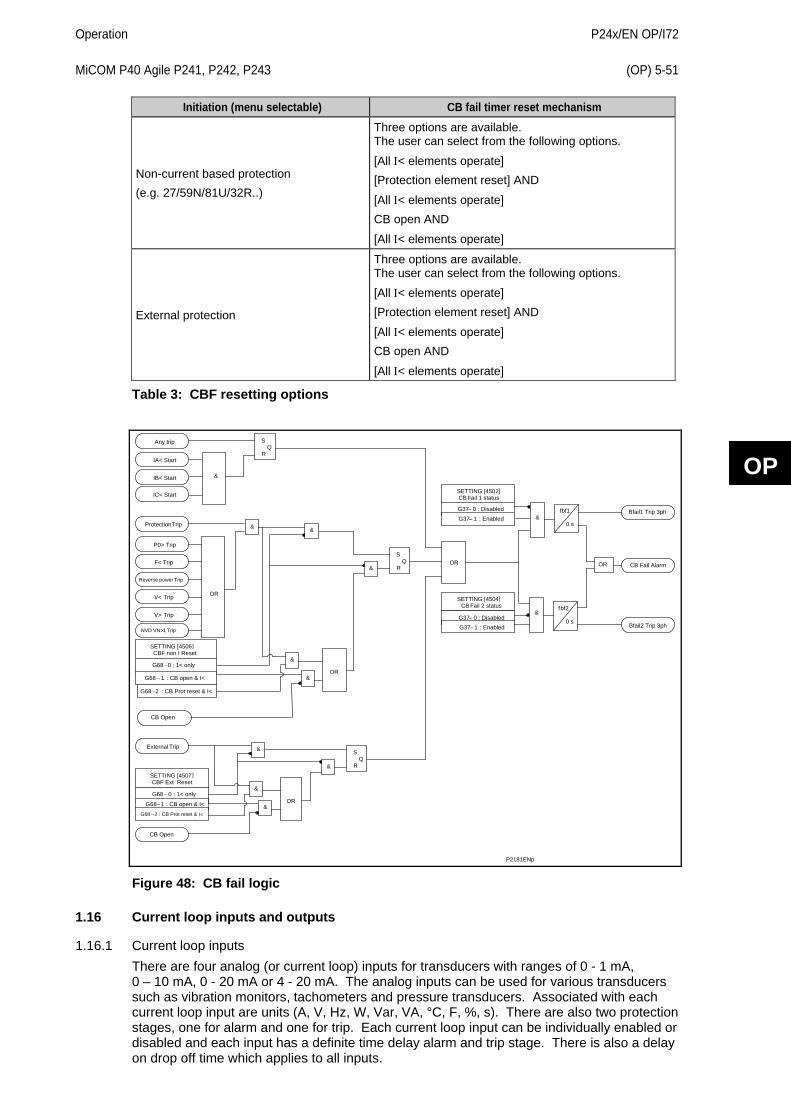
Operation
P24x/EN OP/I72 MiCOM P40 Agile P241, P242, P243 (OP) 5-51
OP
Initiation (menu selectable) CB fail timer reset mechanism
Non-current based protection (e.g. 27/59N/81U/32R..)
Three options are available. The user can select from the following options. [All Ι< elements operate] [Protection element reset] AND [All Ι< elements operate] CB open AND [All Ι< elements operate]
External protection
Three options are available. The user can select from the following options. [All Ι< elements operate] [Protection element reset] AND [All Ι< elements operate] CB open AND
[All Ι< elements operate]
Table 3: CBF resetting options
&
Any trip
P0> Trip
F< Trip
V< Trip
Reverse power Trip
IC< Start
IA< Start
IB< Start
S Q
R
V> Trip
NVD VN>1 Trip
OR
Protection Trip &
SETTING [4507] CBF Ext Reset
G68 – 0 : 1< only
G68 – 1 : CB open & I< G68 – 2 : CB Prot reset & I<
S Q
R
External Trip
CB Open
&
&
OR &
&
S Q
R
CB Open
&
&
&
&
OR
OR
SETTING [4504] CB Fail 2 status
G37 – 0 : Disabled G37 – 1 : Enabled
SETTING [4502] CB Fail 1 status
G37 – 0 : Disabled
G37 – 1 : Enabled
&
&
fbf1
0 s
fbf2
0 s
CB Fail Alarm
Bfail2 Trip 3ph
Bfail1 Trip 3ph
OR
SETTING [4506] CBF non I Reset
G68 – 0 : 1< only
G68 – 1 : CB open & I<
G68 – 2 : CB Prot reset & I<
P2181ENp
Figure 48: CB fail logic
1.16 Current loop inputs and outputs
1.16.1 Current loop inputs There are four analog (or current loop) inputs for transducers with ranges of 0 - 1 mA, 0 – 10 mA, 0 - 20 mA or 4 - 20 mA. The analog inputs can be used for various transducers such as vibration monitors, tachometers and pressure transducers. Associated with each current loop input are units (A, V, Hz, W, Var, VA, °C, F, %, s). There are also two protection stages, one for alarm and one for trip. Each current loop input can be individually enabled or disabled and each input has a definite time delay alarm and trip stage. There is also a delay on drop off time which applies to all inputs.
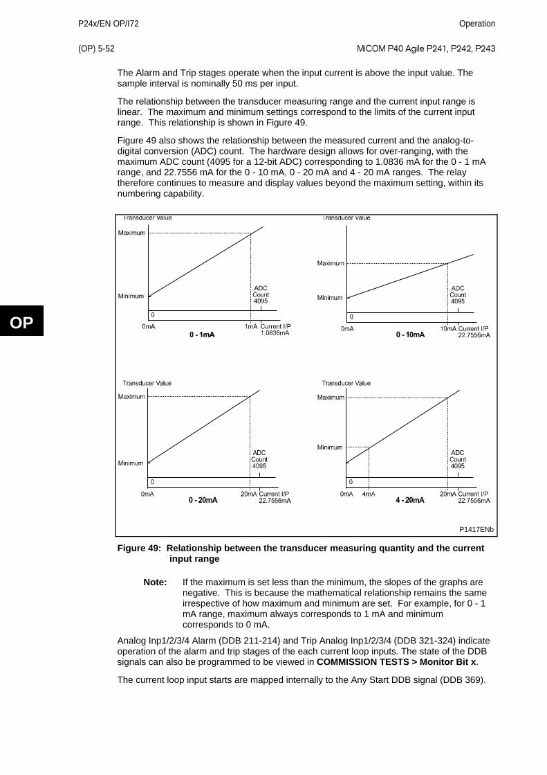
P24x/EN OP/I72
Operation (OP) 5-52 MiCOM P40 Agile P241, P242, P243
OP
The Alarm and Trip stages operate when the input current is above the input value. The sample interval is nominally 50 ms per input.
The relationship between the transducer measuring range and the current input range is linear. The maximum and minimum settings correspond to the limits of the current input range. This relationship is shown in Figure 49.
Figure 49 also shows the relationship between the measured current and the analog-to-digital conversion (ADC) count. The hardware design allows for over-ranging, with the maximum ADC count (4095 for a 12-bit ADC) corresponding to 1.0836 mA for the 0 - 1 mA range, and 22.7556 mA for the 0 - 10 mA, 0 - 20 mA and 4 - 20 mA ranges. The relay therefore continues to measure and display values beyond the maximum setting, within its numbering capability.
P1417ENb
Figure 49: Relationship between the transducer measuring quantity and the current input range
Note: If the maximum is set less than the minimum, the slopes of the graphs are negative. This is because the mathematical relationship remains the same irrespective of how maximum and minimum are set. For example, for 0 - 1 mA range, maximum always corresponds to 1 mA and minimum corresponds to 0 mA.
Analog Inp1/2/3/4 Alarm (DDB 211-214) and Trip Analog Inp1/2/3/4 (DDB 321-324) indicate operation of the alarm and trip stages of the each current loop inputs. The state of the DDB signals can also be programmed to be viewed in COMMISSION TESTS > Monitor Bit x.
The current loop input starts are mapped internally to the Any Start DDB signal (DDB 369).
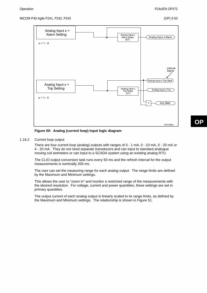
Operation
P24x/EN OP/I72 MiCOM P40 Agile P241, P242, P243 (OP) 5-53
OP
Figure 50: Analog (current loop) input logic diagram
1.16.2 Current loop output There are four current loop (analog) outputs with ranges of 0 - 1 mA, 0 - 10 mA, 0 - 20 mA or 4 - 20 mA. They do not need separate transducers and can input to standard analogue moving coil ammeters or can input to a SCADA system using an existing analog RTU.
The CLIO output conversion task runs every 50 ms and the refresh interval for the output measurements is nominally 200 ms.
The user can set the measuring range for each analog output. The range limits are defined by the Maximum and Minimum settings.
This allows the user to “zoom in” and monitor a restricted range of the measurements with the desired resolution. For voltage, current and power quantities, these settings are set in primary quantities.
The output current of each analog output is linearly scaled to its range limits, as defined by the Maximum and Minimum settings. The relationship is shown in Figure 51.
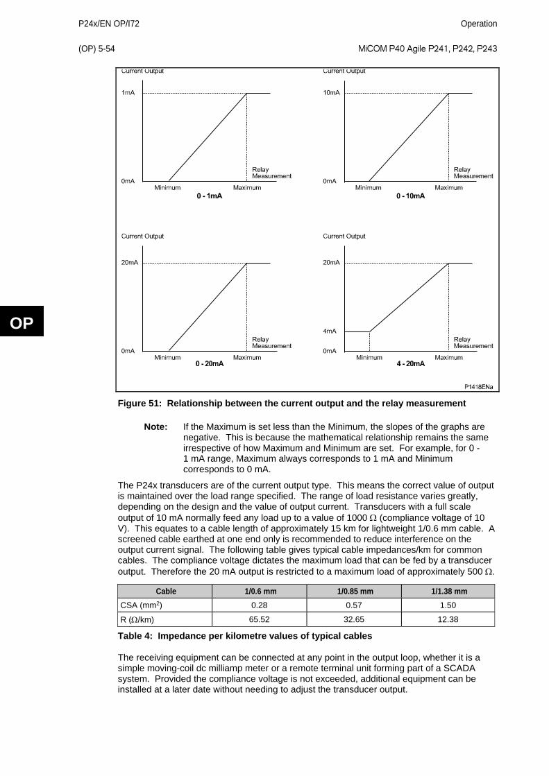
P24x/EN OP/I72
Operation (OP) 5-54 MiCOM P40 Agile P241, P242, P243
OP
Figure 51: Relationship between the current output and the relay measurement
Note: If the Maximum is set less than the Minimum, the slopes of the graphs are negative. This is because the mathematical relationship remains the same irrespective of how Maximum and Minimum are set. For example, for 0 - 1 mA range, Maximum always corresponds to 1 mA and Minimum corresponds to 0 mA.
The P24x transducers are of the current output type. This means the correct value of output is maintained over the load range specified. The range of load resistance varies greatly, depending on the design and the value of output current. Transducers with a full scale output of 10 mA normally feed any load up to a value of 1000 Ω (compliance voltage of 10 V). This equates to a cable length of approximately 15 km for lightweight 1/0.6 mm cable. A screened cable earthed at one end only is recommended to reduce interference on the output current signal. The following table gives typical cable impedances/km for common cables. The compliance voltage dictates the maximum load that can be fed by a transducer output. Therefore the 20 mA output is restricted to a maximum load of approximately 500 Ω.
Cable 1/0.6 mm 1/0.85 mm 1/1.38 mm CSA (mm2) 0.28 0.57 1.50
R (Ω/km) 65.52 32.65 12.38
Table 4: Impedance per kilometre values of typical cables
The receiving equipment can be connected at any point in the output loop, whether it is a simple moving-coil dc milliamp meter or a remote terminal unit forming part of a SCADA system. Provided the compliance voltage is not exceeded, additional equipment can be installed at a later date without needing to adjust the transducer output.
Operation
P24x/EN OP/I72 MiCOM P40 Agile P241, P242, P243 (OP) 5-55
OP
Where the output current range is used for control purposes, it is sometimes worthwhile to fit appropriately rated diodes, or Zener diodes, across the terminals of each of the units in the series loop to guard against the possibility of their internal circuitry becoming open circuit. In this way, a faulty unit in the loop does not cause all the indications to disappear because the constant current nature of the transducer output raises the voltage and continues to force the correct output signal round the loop.
Current loop output parameter Abbreviation Units Range Step Default
min. Defaultmax.
Current Magnitude IA Magnitude IB Magnitude IC Magnitude IN Magnitude
A 0 to 100 k 1 0 100
RMS Phase Currents
IA RMS IB RMS IC RMS IN RMS
A 0 to 100 k 1 0 100
P-N voltage Magnitude
VAN Magnitude VBN Magnitude VCN Magnitude VN Magnitude
V 0 to 20 k 1 0 100
P-N voltage RMS VAN RMS VBN RMS VCN RMS VN RMS
V 0 to 20 k 1 0 100
P-P voltage Magnitude
VAB Magnitude VBC Magnitude VCA Magnitude
V 0 to 20 k 1 0 100
RMS Phase-Phase Voltages
VAB RMS Magnitude VBC RMS Magnitude VCA RMS Magnitude
V 0 to 20 k 1 0 100
Frequency Frequency Hz 0 to 100 1 0 100
3 Ph Active Power Three-Phase Watts W -10 M to 30 M 1 0 100
3 Ph Reactive Power
Three-Phase Vars Var -10 M to 30 M 1 0 100
3 Ph Apparent Power
Three-Phase VA VA -10 M to 30 M 1 0 100
3 Ph Power Factor 3Ph Power Factor -1 to 1 0.01 0 1
RTD Temperatures RTD 1 RTD 2 RTD 3 RTD 4 RTD 5 RTD 6 RTD 7 RTD 8 RTD 9 RTD 10
°C -40 to 400 1 0 100.0
Number of hottest RTD
Nb Hottest RTD 1-10 1 0 10
Thermal State Thermal State % 0 to 150 0.1 0 100
P24x/EN OP/I72
Operation (OP) 5-56 MiCOM P40 Agile P241, P242, P243
OP
Current loop output parameter Abbreviation Units Range Step Default
min. Defaultmax.
Time to Thermal Trip
Time to Thermal Trip Sec 0-300 0.1 0 100
Time to Next Start Time to Next Start Sec 0-300 0.1 0 100
Table 5: Current loop output parameters
Note 1: The current loop (analog) outputs are refreshed every 200 ms.
Note 2: The polarity of Watts, Vars and power factor is affected by the Measurements Mode setting.
Note 3: These settings are for nominal 1 A and 100/120 V versions only. For other nominal versions they need to be multiplied accordingly.
Note 4: All current loop (analog) output measurements are in primary values.
Operation
P24x/EN OP/I72 MiCOM P40 Agile P241, P242, P243 (OP) 5-57
OP
2 OPERATION OF NON PROTECTION FUNCTIONS
2.1 VT supervision The voltage transformer supervision (VTS) feature is used to detect failure of the ac voltage inputs to the relay. This may be caused by internal voltage transformer faults, overloading, or faults on the interconnecting wiring to relays. This usually results in one or more VT fuses blowing. Following a failure of the ac voltage input there would be a misrepresentation of the phase voltages on the power system as measured by the relay, which may result in mal-operation.
The VTS logic in the relay detects the voltage failure and automatically adjusts the configuration of protection elements whose stability would otherwise be compromised. A time-delayed alarm output is also available.
There are three main aspects to consider if there is a failure of the VT supply.
• Loss of one or two-phase voltages
• Loss of all three-phase voltages under load conditions
• Absence of three-phase voltages on line energization
The VTS feature in the relay operates if it detects negative phase sequence (NPS) voltage when there is no negative phase sequence current. This gives operation for the loss of one or two-phase voltages. Stability of the VTS function is assured during system fault conditions by the presence of NPS current. The use of negative sequence quantities ensures correct operation even where three-limb or ‘V’ connected VTs are used.
Negative sequence VTS element:
The negative sequence thresholds used by the element are V2 = 10 V and Ι2 = 0.05 to 0.5 Ιn settable (defaulted to 0.05 Ιn).
2.1.1 Loss of all three-phase voltages under load conditions If all three-phase voltages to the relay are lost, there are no negative phase sequence quantities present to operate the VTS function and the three-phase voltages collapse. If this is detected without a corresponding change in any of the phase current signals (which would indicate a fault), a VTS condition is raised. In practice, the relay detects the presence of superimposed current signals, which are changes in the current applied to the relay. These signals are generated by comparing the present value of the current with that exactly one cycle previously. Under normal load conditions, the value of superimposed current should therefore be zero. Under a fault condition, a superimposed current signal is generated which prevents the VTS from operating.
Use Threshold 3P to set the phase voltage level detector from 10 V to 70 V (default 30 V).
Use Delta I> to set the sensitivity of the superimposed current elements from 0.1 In to 5 In (default 0.1 In).
2.1.2 Absence of three-phase voltages on line energization If a VT is inadvertently left isolated before the line is energized, voltage dependent elements could operate incorrectly. The previous VTS element detected three-phase VT failure by the absence of all three-phase voltages, with no corresponding change in current. When the line is energized there is a change in current, for example due to load or line charging current. An alternative method of detecting three-phase VT failure is therefore required when the line is energized.
The absence of measured voltage on all three phases when the line is energized can be due to a three-phase VT failure or a close up three-phase fault. The first condition requires the voltage dependent function to be blocked and the second requires tripping. To differentiate between these two conditions an overcurrent level detector (VTS Ι> Inhibit) prevents a VTS block from being issued if it operates. This element should be set in excess of any non-fault based currents on line energization (load, line charging current, transformer inrush current if applicable) but below the level of current produced by a close up three-phase fault. If the line is then closed where a three-phase VT failure is present, the overcurrent detector does
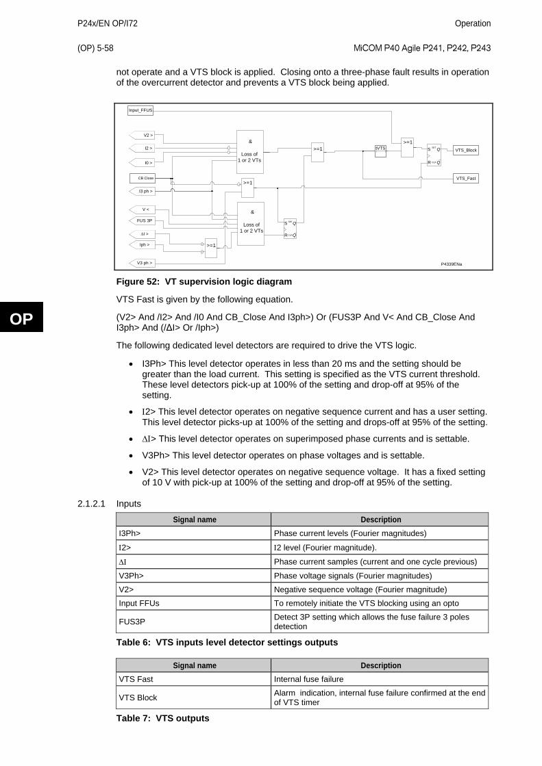
P24x/EN OP/I72
Operation (OP) 5-58 MiCOM P40 Agile P241, P242, P243
OP
not operate and a VTS block is applied. Closing onto a three-phase fault results in operation of the overcurrent detector and prevents a VTS block being applied.
P4339ENa
tVTS
Input_FFUS
I3 ph >
VTS_Block
VTS_Fast
>=1
>=1
>=1
Loss of1 or 2 VTs
&
Loss of1 or 2 VTs
&
>=1
Q
QSET
CLR
S
R
Q
QSET
CLR
S
R
V2 >
I2 >
I0 >
CB Close
V <
FUS 3P
∆I >
Iph >
V3 ph >
Figure 52: VT supervision logic diagram
VTS Fast is given by the following equation.
(V2> And /I2> And /I0 And CB_Close And I3ph>) Or (FUS3P And V< And CB_Close And I3ph> And (/ΔI> Or /Iph>)
The following dedicated level detectors are required to drive the VTS logic.
• I3Ph> This level detector operates in less than 20 ms and the setting should be greater than the load current. This setting is specified as the VTS current threshold. These level detectors pick-up at 100% of the setting and drop-off at 95% of the setting.
• Ι2> This level detector operates on negative sequence current and has a user setting. This level detector picks-up at 100% of the setting and drops-off at 95% of the setting.
• ∆Ι> This level detector operates on superimposed phase currents and is settable.
• V3Ph> This level detector operates on phase voltages and is settable.
• V2> This level detector operates on negative sequence voltage. It has a fixed setting of 10 V with pick-up at 100% of the setting and drop-off at 95% of the setting.
2.1.2.1 Inputs
Signal name Description I3Ph> Phase current levels (Fourier magnitudes)
Ι2> Ι2 level (Fourier magnitude).
∆Ι Phase current samples (current and one cycle previous)
V3Ph> Phase voltage signals (Fourier magnitudes)
V2> Negative sequence voltage (Fourier magnitude)
Input FFUs To remotely initiate the VTS blocking using an opto
FUS3P Detect 3P setting which allows the fuse failure 3 poles detection
Table 6: VTS inputs level detector settings outputs
Signal name Description VTS Fast Internal fuse failure
VTS Block Alarm indication, internal fuse failure confirmed at the end of VTS timer
Table 7: VTS outputs
Operation
P24x/EN OP/I72 MiCOM P40 Agile P241, P242, P243 (OP) 5-59
OP
2.1.3 Operation The relay may respond as follows to an operation of any VTS element:
• Forced blocking of voltage dependent protection elements (DDB 364 VT Supervision, Fast Block and DDB 363 VT, confirmed block)
• VTS provides alarm indication (DDB 363 VT, confirmed block). The confirmed fuse failure VTS_Block blocks the following protection functions:
Undervoltage Positive sequence undervoltage Loss of load Reverse power Residual Overvoltage Wattmetric SEF Reacceleration (if enabled) Overcurrent DEF (if directional is used) Overcurrent SEF (if directional is used)
Functions which use the directional element are blocked if set as directional:
• IN> VTS Blocking = xx for each stage. When the relevant bit is set to 1, operation of VTS blocks the stage if directionalised. When set to 0 the function is set to Non-directional.
• ISEF> VTS Blocking = xx for each stage. When the relevant bit is set to 1, operation of VTS blocks the stage if directionalised. When set to 0 the function is set to Non-directional.
The internal fuse failure VTS_Fast blocks the same functions but if a fault is detected before the confirmation timer is issued, the functions are unblocked. The fault can be detected by the criteria Iph>, I2>, I0> and ΔI>.
The VTS Ι> Inhibit element is used to override a VTS block if a fault occurs on the system which could trigger the VTS logic. Once the VTS block has been established, subsequent system faults should not override the block. The VTS block is therefore latched after a user settable time delay VTS Time Delay. Once the signal has latched, it is reset automatically by CB Open or by the three-phase voltages returning above the phase detector level settings.
A VTS indication is given after the VTS Time Delay has expired.
If a miniature circuit breaker (MCB) is used to protect the voltage transformer ac output circuits, use MCB auxiliary contacts to indicate a three-phase output disconnection. The VTS logic can operate correctly without this input. However, this facility provides compatibility with current practices of various utilities. Energizing an opto-isolated input assigned to DDB 362 MCB/VTS on the relay provides the necessary block.
The blocking of the VTS logic for a number of different fault conditions is considered below.
1. Phase-phase fault
The I2> element detects phase-phase faults when the CB is closed and blocks the VTS logic.
2. Three phase faults
The delta current level detectors detect the change in current for a close up 3 phase fault when the CB is closed and block the VTS.
The IPh> level detector detects a 3 phase fault when closing the CB onto a fault and blocks the VTS logic.
2.2 CT supervision The CT supervision feature operates when it detects derived residual current, without the corresponding derived or measured residual voltage that would normally accompany it.
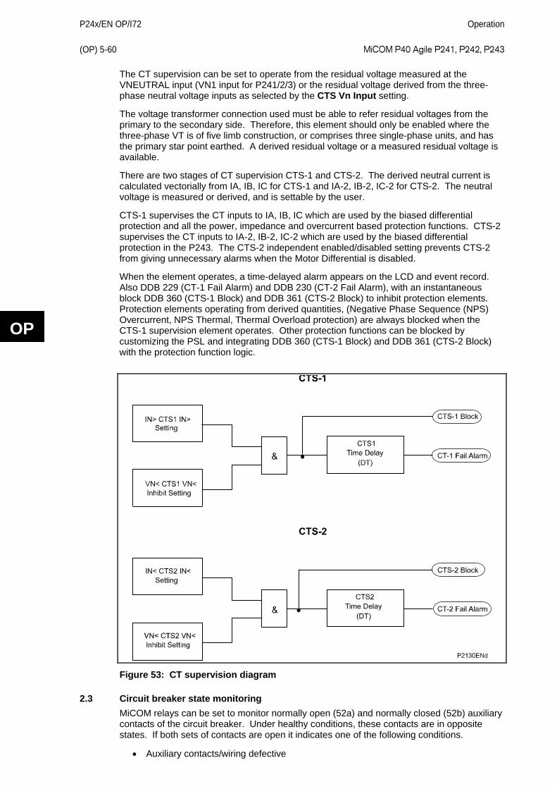
P24x/EN OP/I72
Operation (OP) 5-60 MiCOM P40 Agile P241, P242, P243
OP
The CT supervision can be set to operate from the residual voltage measured at the VNEUTRAL input (VN1 input for P241/2/3) or the residual voltage derived from the three-phase neutral voltage inputs as selected by the CTS Vn Input setting.
The voltage transformer connection used must be able to refer residual voltages from the primary to the secondary side. Therefore, this element should only be enabled where the three-phase VT is of five limb construction, or comprises three single-phase units, and has the primary star point earthed. A derived residual voltage or a measured residual voltage is available.
There are two stages of CT supervision CTS-1 and CTS-2. The derived neutral current is calculated vectorially from IA, IB, IC for CTS-1 and IA-2, IB-2, IC-2 for CTS-2. The neutral voltage is measured or derived, and is settable by the user.
CTS-1 supervises the CT inputs to IA, IB, IC which are used by the biased differential protection and all the power, impedance and overcurrent based protection functions. CTS-2 supervises the CT inputs to IA-2, IB-2, IC-2 which are used by the biased differential protection in the P243. The CTS-2 independent enabled/disabled setting prevents CTS-2 from giving unnecessary alarms when the Motor Differential is disabled.
When the element operates, a time-delayed alarm appears on the LCD and event record. Also DDB 229 (CT-1 Fail Alarm) and DDB 230 (CT-2 Fail Alarm), with an instantaneous block DDB 360 (CTS-1 Block) and DDB 361 (CTS-2 Block) to inhibit protection elements. Protection elements operating from derived quantities, (Negative Phase Sequence (NPS) Overcurrent, NPS Thermal, Thermal Overload protection) are always blocked when the CTS-1 supervision element operates. Other protection functions can be blocked by customizing the PSL and integrating DDB 360 (CTS-1 Block) and DDB 361 (CTS-2 Block) with the protection function logic.
Figure 53: CT supervision diagram
2.3 Circuit breaker state monitoring MiCOM relays can be set to monitor normally open (52a) and normally closed (52b) auxiliary contacts of the circuit breaker. Under healthy conditions, these contacts are in opposite states. If both sets of contacts are open it indicates one of the following conditions.
• Auxiliary contacts/wiring defective
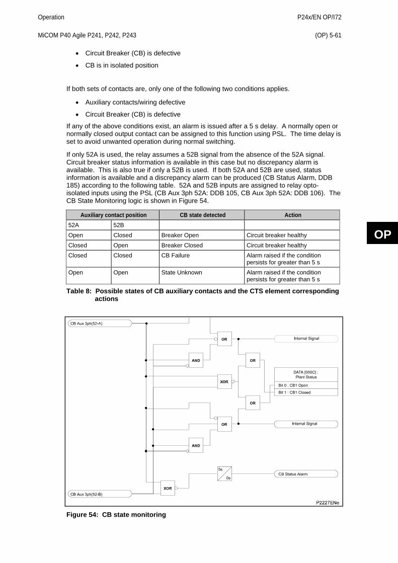
Operation
P24x/EN OP/I72 MiCOM P40 Agile P241, P242, P243 (OP) 5-61
OP
• Circuit Breaker (CB) is defective
• CB is in isolated position
If both sets of contacts are, only one of the following two conditions applies.
• Auxiliary contacts/wiring defective
• Circuit Breaker (CB) is defective
If any of the above conditions exist, an alarm is issued after a 5 s delay. A normally open or normally closed output contact can be assigned to this function using PSL. The time delay is set to avoid unwanted operation during normal switching.
If only 52A is used, the relay assumes a 52B signal from the absence of the 52A signal. Circuit breaker status information is available in this case but no discrepancy alarm is available. This is also true if only a 52B is used. If both 52A and 52B are used, status information is available and a discrepancy alarm can be produced (CB Status Alarm, DDB 185) according to the following table. 52A and 52B inputs are assigned to relay opto-isolated inputs using the PSL (CB Aux 3ph 52A: DDB 105, CB Aux 3ph 52A: DDB 106). The CB State Monitoring logic is shown in Figure 54.
Auxiliary contact position CB state detected Action 52A 52B
Open Closed Breaker Open Circuit breaker healthy
Closed Open Breaker Closed Circuit breaker healthy
Closed Closed CB Failure Alarm raised if the condition persists for greater than 5 s
Open Open State Unknown Alarm raised if the condition persists for greater than 5 s
Table 8: Possible states of CB auxiliary contacts and the CTS element corresponding actions
Figure 54: CB state monitoring
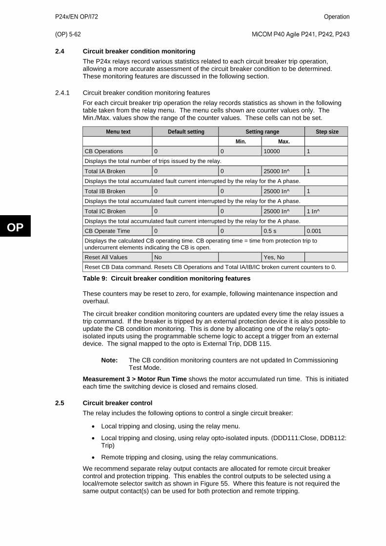
P24x/EN OP/I72
Operation (OP) 5-62 MiCOM P40 Agile P241, P242, P243
OP
2.4 Circuit breaker condition monitoring The P24x relays record various statistics related to each circuit breaker trip operation, allowing a more accurate assessment of the circuit breaker condition to be determined. These monitoring features are discussed in the following section.
2.4.1 Circuit breaker condition monitoring features For each circuit breaker trip operation the relay records statistics as shown in the following table taken from the relay menu. The menu cells shown are counter values only. The Min./Max. values show the range of the counter values. These cells can not be set.
Menu text Default setting Setting range Step size Min. Max.
CB Operations 0 0 10000 1
Displays the total number of trips issued by the relay.
Total ΙA Broken 0 0 25000 Ιn^ 1
Displays the total accumulated fault current interrupted by the relay for the A phase.
Total ΙB Broken 0 0 25000 Ιn^ 1
Displays the total accumulated fault current interrupted by the relay for the A phase.
Total ΙC Broken 0 0 25000 Ιn^ 1 Ιn^
Displays the total accumulated fault current interrupted by the relay for the A phase.
CB Operate Time 0 0 0.5 s 0.001
Displays the calculated CB operating time. CB operating time = time from protection trip to undercurrent elements indicating the CB is open.
Reset All Values No Yes, No
Reset CB Data command. Resets CB Operations and Total IA/IB/IC broken current counters to 0.
Table 9: Circuit breaker condition monitoring features
These counters may be reset to zero, for example, following maintenance inspection and overhaul.
The circuit breaker condition monitoring counters are updated every time the relay issues a trip command. If the breaker is tripped by an external protection device it is also possible to update the CB condition monitoring. This is done by allocating one of the relay’s opto-isolated inputs using the programmable scheme logic to accept a trigger from an external device. The signal mapped to the opto is External Trip, DDB 115.
Note: The CB condition monitoring counters are not updated In Commissioning Test Mode.
Measurement 3 > Motor Run Time shows the motor accumulated run time. This is initiated each time the switching device is closed and remains closed.
2.5 Circuit breaker control The relay includes the following options to control a single circuit breaker:
• Local tripping and closing, using the relay menu.
• Local tripping and closing, using relay opto-isolated inputs. (DDD111:Close, DDB112: Trip)
• Remote tripping and closing, using the relay communications.
We recommend separate relay output contacts are allocated for remote circuit breaker control and protection tripping. This enables the control outputs to be selected using a local/remote selector switch as shown in Figure 55. Where this feature is not required the same output contact(s) can be used for both protection and remote tripping.
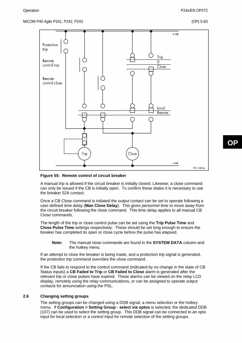
Operation
P24x/EN OP/I72 MiCOM P40 Agile P241, P242, P243 (OP) 5-63
OP
Figure 55: Remote control of circuit breaker
A manual trip is allowed if the circuit breaker is initially closed. Likewise, a close command can only be issued if the CB is initially open. To confirm these states it is necessary to use the breaker 52A contact.
Once a CB Close command is initiated the output contact can be set to operate following a user-defined time delay (Man Close Delay). This gives personnel time to move away from the circuit breaker following the close command. This time delay applies to all manual CB Close commands.
The length of the trip or close control pulse can be set using the Trip Pulse Time and Close Pulse Time settings respectively. These should be set long enough to ensure the breaker has completed its open or close cycle before the pulse has elapsed.
Note: The manual close commands are found in the SYSTEM DATA column and the hotkey menu.
If an attempt to close the breaker is being made, and a protection trip signal is generated, the protection trip command overrides the close command.
If the CB fails to respond to the control command (indicated by no change in the state of CB Status inputs) a CB Failed to Trip or CB Failed to Close alarm is generated after the relevant trip or close pulses have expired. These alarms can be viewed on the relay LCD display, remotely using the relay communications, or can be assigned to operate output contacts for annunciation using the PSL.
2.6 Changing setting groups The setting groups can be changed using a DDB signal, a menu selection or the hotkey menu. If Configuration > Setting Group - select via optos is selected, the dedicated DDB (107) can be used to select the setting group. This DDB signal can be connected to an opto input for local selection or a control input for remote selection of the setting groups.
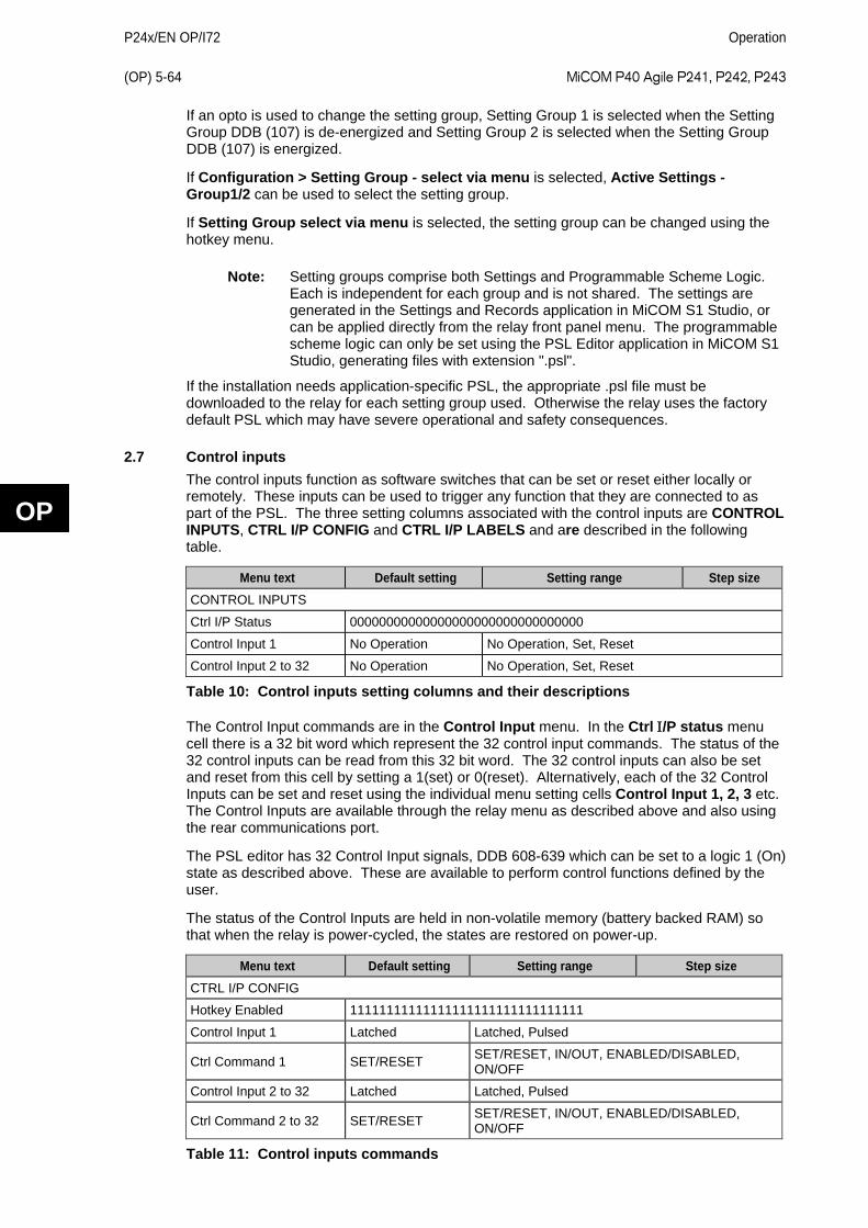
P24x/EN OP/I72
Operation (OP) 5-64 MiCOM P40 Agile P241, P242, P243
OP
If an opto is used to change the setting group, Setting Group 1 is selected when the Setting Group DDB (107) is de-energized and Setting Group 2 is selected when the Setting Group DDB (107) is energized.
If Configuration > Setting Group - select via menu is selected, Active Settings - Group1/2 can be used to select the setting group.
If Setting Group select via menu is selected, the setting group can be changed using the hotkey menu.
Note: Setting groups comprise both Settings and Programmable Scheme Logic. Each is independent for each group and is not shared. The settings are generated in the Settings and Records application in MiCOM S1 Studio, or can be applied directly from the relay front panel menu. The programmable scheme logic can only be set using the PSL Editor application in MiCOM S1 Studio, generating files with extension ".psl".
If the installation needs application-specific PSL, the appropriate .psl file must be downloaded to the relay for each setting group used. Otherwise the relay uses the factory default PSL which may have severe operational and safety consequences.
2.7 Control inputs The control inputs function as software switches that can be set or reset either locally or remotely. These inputs can be used to trigger any function that they are connected to as part of the PSL. The three setting columns associated with the control inputs are CONTROL INPUTS, CTRL I/P CONFIG and CTRL I/P LABELS and are described in the following table.
Menu text Default setting Setting range Step size CONTROL INPUTS
Ctrl I/P Status 00000000000000000000000000000000
Control Input 1 No Operation No Operation, Set, Reset
Control Input 2 to 32 No Operation No Operation, Set, Reset
Table 10: Control inputs setting columns and their descriptions
The Control Input commands are in the Control Input menu. In the Ctrl Ι/P status menu cell there is a 32 bit word which represent the 32 control input commands. The status of the 32 control inputs can be read from this 32 bit word. The 32 control inputs can also be set and reset from this cell by setting a 1(set) or 0(reset). Alternatively, each of the 32 Control Inputs can be set and reset using the individual menu setting cells Control Input 1, 2, 3 etc. The Control Inputs are available through the relay menu as described above and also using the rear communications port.
The PSL editor has 32 Control Input signals, DDB 608-639 which can be set to a logic 1 (On) state as described above. These are available to perform control functions defined by the user.
The status of the Control Inputs are held in non-volatile memory (battery backed RAM) so that when the relay is power-cycled, the states are restored on power-up.
Menu text Default setting Setting range Step size CTRL I/P CONFIG
Hotkey Enabled 11111111111111111111111111111111
Control Input 1 Latched Latched, Pulsed
Ctrl Command 1 SET/RESET SET/RESET, IN/OUT, ENABLED/DISABLED, ON/OFF
Control Input 2 to 32 Latched Latched, Pulsed
Ctrl Command 2 to 32 SET/RESET SET/RESET, IN/OUT, ENABLED/DISABLED, ON/OFF
Table 11: Control inputs commands
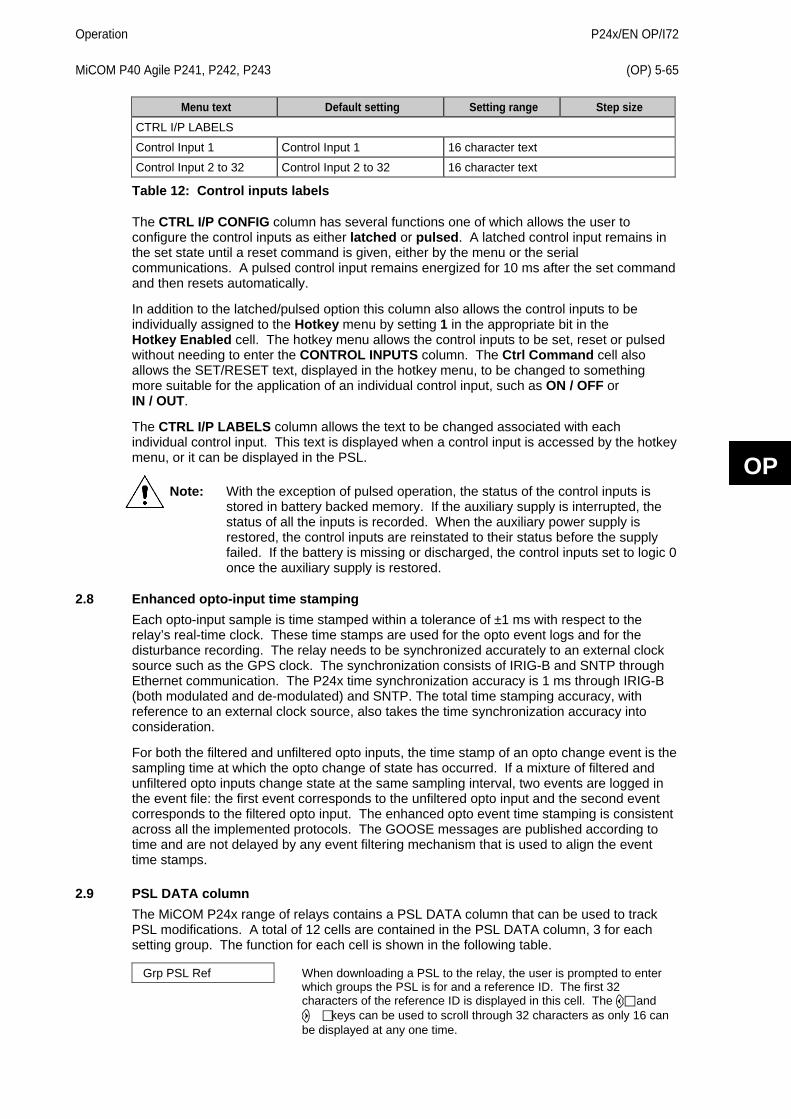
Operation
P24x/EN OP/I72 MiCOM P40 Agile P241, P242, P243 (OP) 5-65
OP
Menu text Default setting Setting range Step size CTRL I/P LABELS
Control Input 1 Control Input 1 16 character text
Control Input 2 to 32 Control Input 2 to 32 16 character text
Table 12: Control inputs labels
The CTRL I/P CONFIG column has several functions one of which allows the user to configure the control inputs as either latched or pulsed. A latched control input remains in the set state until a reset command is given, either by the menu or the serial communications. A pulsed control input remains energized for 10 ms after the set command and then resets automatically.
In addition to the latched/pulsed option this column also allows the control inputs to be individually assigned to the Hotkey menu by setting 1 in the appropriate bit in the Hotkey Enabled cell. The hotkey menu allows the control inputs to be set, reset or pulsed without needing to enter the CONTROL INPUTS column. The Ctrl Command cell also allows the SET/RESET text, displayed in the hotkey menu, to be changed to something more suitable for the application of an individual control input, such as ON / OFF or IN / OUT.
The CTRL I/P LABELS column allows the text to be changed associated with each individual control input. This text is displayed when a control input is accessed by the hotkey menu, or it can be displayed in the PSL.
Note: With the exception of pulsed operation, the status of the control inputs is stored in battery backed memory. If the auxiliary supply is interrupted, the status of all the inputs is recorded. When the auxiliary power supply is restored, the control inputs are reinstated to their status before the supply failed. If the battery is missing or discharged, the control inputs set to logic 0 once the auxiliary supply is restored.
2.8 Enhanced opto-input time stamping Each opto-input sample is time stamped within a tolerance of ±1 ms with respect to the relay’s real-time clock. These time stamps are used for the opto event logs and for the disturbance recording. The relay needs to be synchronized accurately to an external clock source such as the GPS clock. The synchronization consists of IRIG-B and SNTP through Ethernet communication. The P24x time synchronization accuracy is 1 ms through IRIG-B (both modulated and de-modulated) and SNTP. The total time stamping accuracy, with reference to an external clock source, also takes the time synchronization accuracy into consideration.
For both the filtered and unfiltered opto inputs, the time stamp of an opto change event is the sampling time at which the opto change of state has occurred. If a mixture of filtered and unfiltered opto inputs change state at the same sampling interval, two events are logged in the event file: the first event corresponds to the unfiltered opto input and the second event corresponds to the filtered opto input. The enhanced opto event time stamping is consistent across all the implemented protocols. The GOOSE messages are published according to time and are not delayed by any event filtering mechanism that is used to align the event time stamps.
2.9 PSL DATA column The MiCOM P24x range of relays contains a PSL DATA column that can be used to track PSL modifications. A total of 12 cells are contained in the PSL DATA column, 3 for each setting group. The function for each cell is shown in the following table.
Grp PSL Ref When downloading a PSL to the relay, the user is prompted to enter which groups the PSL is for and a reference ID. The first 32 characters of the reference ID is displayed in this cell. The and keys can be used to scroll through 32 characters as only 16 can be displayed at any one time.

P24x/EN OP/I72
Operation (OP) 5-66 MiCOM P40 Agile P241, P242, P243
OP
18 Nov 2002 08:59:32.047
This cell displays the date and time when the PSL was down loaded to the relay.
Grp 1 PSL ID – 2062813232
This is a unique number for the PSL that has been entered. Any change in the PSL results in a different number being displayed.
Note: The above cells are repeated for each setting group.
2.10 Reset of programmable LEDs and output contacts The programmable LEDs and output contacts can be set to be latched in the programmable scheme logic. If there is a fault record, clearing the fault record by pressing the key once the fault record has been read clears any latched LEDs and output contacts. If there is no fault record, as long as the initiating signal to the LED or output contact is reset, the LEDs and contacts can be reset by one of the following methods.
• Using the View Records - Reset Indications menu command cell.
• Using DDB 113 Reset Latches which can be mapped to an Opto Input or a Control Input for example.
2.11 Real time clock synchronization using opto-inputs Protective schemes often need the real time clock of the relays to be synchronized so that events from different relays can be placed in chronological order. This can be done using the IRIG-B input, if fitted, or the communication interface connected to the substation control system. The P24x can also be synchronized using an opto-input by routing it in PSL to DDB 116 (Time Sync.). Pulsing this input results in the real time clock snapping to the nearest minute if the pulse input is ± 3 s of the relay clock time. If the real time clock is within 3 s of the pulse, over a short period the relay clock slows down or speeds up to the correct time. The recommended pulse duration is 20 ms to be repeated no more than once per minute. An example of the time sync function is shown below.
Time of “Sync. Pulse” Corrected time 19:47:00 to 19:47:29 19:47:00
19:47:30 to 19:47:59 19:48:00
Table 13: Example of time sync by using opto-inputs
Note: The above assumes a time format of hh:mm:ss
To avoid the event buffer from being filled with unnecessary time sync. events, it is possible to ignore any event that generated by the time sync. opto input. This can be done by applying the following settings.
Menu text Value RECORD CONTROL
Opto Input Event Enabled
Protection Event Enabled
DDB 064 - 079 (Opto Inputs) Set “Time Sync.” associated opto to 0
Table 14: Setting example to avoid event buffer overflow
To improve the recognition time of the time sync. opto input by approximately 10 ms, the opto input filtering could be disabled. To do this, in OPTO CONFIG > Opto Filter Cntl set the appropriate bit to 0.
Disabling the filtering may make the opto input more susceptible to induced noise. This can be minimized as described in section 2.3.3 of the Firmware Design chapter (P24x/EN FD).
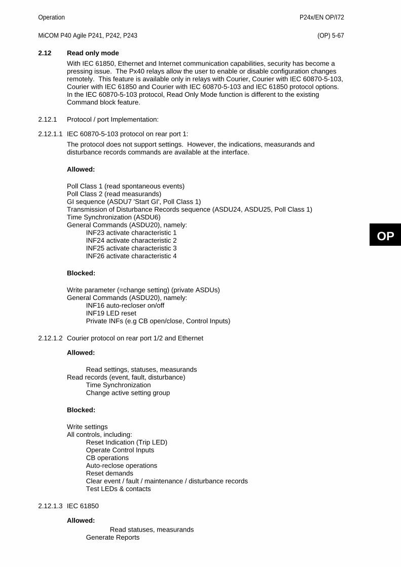
Operation
P24x/EN OP/I72 MiCOM P40 Agile P241, P242, P243 (OP) 5-67
OP
2.12 Read only mode With IEC 61850, Ethernet and Internet communication capabilities, security has become a pressing issue. The Px40 relays allow the user to enable or disable configuration changes remotely. This feature is available only in relays with Courier, Courier with IEC 60870-5-103, Courier with IEC 61850 and Courier with IEC 60870-5-103 and IEC 61850 protocol options. In the IEC 60870-5-103 protocol, Read Only Mode function is different to the existing Command block feature.
2.12.1 Protocol / port Implementation:
2.12.1.1 IEC 60870-5-103 protocol on rear port 1: The protocol does not support settings. However, the indications, measurands and disturbance records commands are available at the interface.
Allowed: Poll Class 1 (read spontaneous events) Poll Class 2 (read measurands) GI sequence (ASDU7 'Start GI', Poll Class 1) Transmission of Disturbance Records sequence (ASDU24, ASDU25, Poll Class 1) Time Synchronization (ASDU6) General Commands (ASDU20), namely: INF23 activate characteristic 1 INF24 activate characteristic 2 INF25 activate characteristic 3 INF26 activate characteristic 4
Blocked: Write parameter (=change setting) (private ASDUs) General Commands (ASDU20), namely: INF16 auto-recloser on/off INF19 LED reset Private INFs (e.g CB open/close, Control Inputs)
2.12.1.2 Courier protocol on rear port 1/2 and Ethernet
Allowed: Read settings, statuses, measurands Read records (event, fault, disturbance) Time Synchronization Change active setting group
Blocked: Write settings All controls, including: Reset Indication (Trip LED) Operate Control Inputs CB operations Auto-reclose operations Reset demands Clear event / fault / maintenance / disturbance records Test LEDs & contacts
2.12.1.3 IEC 61850
Allowed: Read statuses, measurands Generate Reports
P24x/EN OP/I72
Operation (OP) 5-68 MiCOM P40 Agile P241, P242, P243
OP
Extract Disturbance Records Time Synchronization Change active setting group
Blocked: All controls, including: Enable / Disable protection Operate Control Inputs CB operations (Close / Trip, Lock) Reset LEDs
2.12.1.4 Courier database support Three new settings, one for each remote communications port at the back of the relay allow the read only mode at each port to be enabled or disabled.
The NIC Read Only setting applies to all the communications protocols transmitted using the Ethernet Port, including the Tunnelled Courier. Their default values are Disabled.
The Modbus and DNP3 communications interfaces that do not support the feature ignore these settings.
2.12.2 New DDB signals The remote read only mode can be used in the PSL with the following dedicated DDB signals.
• RP1 Read Only
• RP2 Read Only
• NIC Read Only
These read-only DDB signals can be used with Opto Inputs, Control Inputs and Function Keys. They are available in every build, however they are effective only in Courier, IEC 60870-5-103 build and in IEC 61850 firmware version 42 onwards. The setting cells are not available in Modbus and DNP3.0.
2.13 Any trip The Any Trip DDB (DDB 371) is a combination of all the individual trip signals. This DDB has been made independent from relay 3 in the version C2.0 software and later. In the previous versions of software the Any Trip signal was the operation of Relay 3. In the version C2.0 software and later DDB371 is the Any Trip signal and any output contact used for tripping can be connected to the Any Trip DDB leaving Relay 3 to be freely assigned for any function. The Any Trip signal affects the following functions:
• Operates the Trip LED
• Triggers CB condition maintenance counters
• Used to measure the CB operating time
• Triggers the circuit breaker failure logic
• Used in the Fault recorder logic
In the default PSL, Relay 3 is still mapped to the Any Trip DDB and Trip LED DDB as well as the Fault REC TRIG DDB signals as shown in the PSL diagram below.
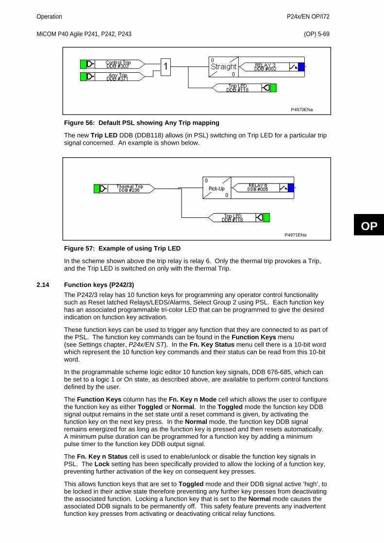
Operation
P24x/EN OP/I72 MiCOM P40 Agile P241, P242, P243 (OP) 5-69
OP
P4970ENa
Figure 56: Default PSL showing Any Trip mapping
The new Trip LED DDB (DDB118) allows (in PSL) switching on Trip LED for a particular trip signal concerned. An example is shown below.
P4971ENa
Figure 57: Example of using Trip LED
In the scheme shown above the trip relay is relay 6. Only the thermal trip provokes a Trip, and the Trip LED is switched on only with the thermal Trip.
2.14 Function keys (P242/3) The P242/3 relay has 10 function keys for programming any operator control functionality such as Reset latched Relays/LEDS/Alarms, Select Group 2 using PSL. Each function key has an associated programmable tri-color LED that can be programmed to give the desired indication on function key activation.
These function keys can be used to trigger any function that they are connected to as part of the PSL. The function key commands can be found in the Function Keys menu (see Settings chapter, P24x/EN ST). In the Fn. Key Status menu cell there is a 10-bit word which represent the 10 function key commands and their status can be read from this 10-bit word.
In the programmable scheme logic editor 10 function key signals, DDB 676-685, which can be set to a logic 1 or On state, as described above, are available to perform control functions defined by the user.
The Function Keys column has the Fn. Key n Mode cell which allows the user to configure the function key as either Toggled or Normal. In the Toggled mode the function key DDB signal output remains in the set state until a reset command is given, by activating the function key on the next key press. In the Normal mode, the function key DDB signal remains energized for as long as the function key is pressed and then resets automatically. A minimum pulse duration can be programmed for a function key by adding a minimum pulse timer to the function key DDB output signal.
The Fn. Key n Status cell is used to enable/unlock or disable the function key signals in PSL. The Lock setting has been specifically provided to allow the locking of a function key, preventing further activation of the key on consequent key presses.
This allows function keys that are set to Toggled mode and their DDB signal active ‘high’, to be locked in their active state therefore preventing any further key presses from deactivating the associated function. Locking a function key that is set to the Normal mode causes the associated DDB signals to be permanently off. This safety feature prevents any inadvertent function key presses from activating or deactivating critical relay functions.
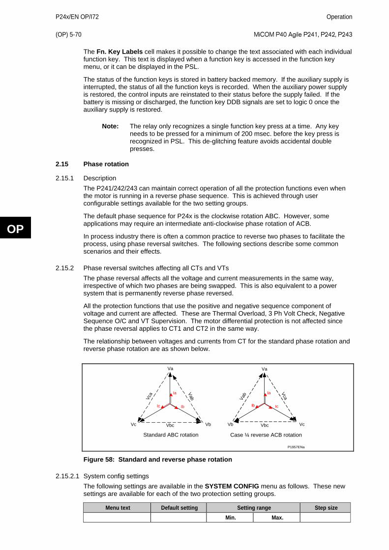
P24x/EN OP/I72
Operation (OP) 5-70 MiCOM P40 Agile P241, P242, P243
OP
The Fn. Key Labels cell makes it possible to change the text associated with each individual function key. This text is displayed when a function key is accessed in the function key menu, or it can be displayed in the PSL.
The status of the function keys is stored in battery backed memory. If the auxiliary supply is interrupted, the status of all the function keys is recorded. When the auxiliary power supply is restored, the control inputs are reinstated to their status before the supply failed. If the battery is missing or discharged, the function key DDB signals are set to logic 0 once the auxiliary supply is restored.
Note: The relay only recognizes a single function key press at a time. Any key needs to be pressed for a minimum of 200 msec. before the key press is recognized in PSL. This de-glitching feature avoids accidental double presses.
2.15 Phase rotation
2.15.1 Description The P241/242/243 can maintain correct operation of all the protection functions even when the motor is running in a reverse phase sequence. This is achieved through user configurable settings available for the two setting groups.
The default phase sequence for P24x is the clockwise rotation ABC. However, some applications may require an intermediate anti-clockwise phase rotation of ACB.
In process industry there is often a common practice to reverse two phases to facilitate the process, using phase reversal switches. The following sections describe some common scenarios and their effects.
2.15.2 Phase reversal switches affecting all CTs and VTs The phase reversal affects all the voltage and current measurements in the same way, irrespective of which two phases are being swapped. This is also equivalent to a power system that is permanently reverse phase reversed.
All the protection functions that use the positive and negative sequence component of voltage and current are affected. These are Thermal Overload, 3 Ph Volt Check, Negative Sequence O/C and VT Supervision. The motor differential protection is not affected since the phase reversal applies to CT1 and CT2 in the same way.
The relationship between voltages and currents from CT for the standard phase rotation and reverse phase rotation are as shown below.
Standard ABC rotation
Vc VbVbc
Vca
Va
Vab
Ia
IbIc
Case ¼ reverse ACB rotation
Vb VcVbc
Va
Ia
IcIb
Vab Vca
P1957ENa
Figure 58: Standard and reverse phase rotation
2.15.2.1 System config settings The following settings are available in the SYSTEM CONFIG menu as follows. These new settings are available for each of the two protection setting groups.
Menu text Default setting Setting range Step size Min. Max.
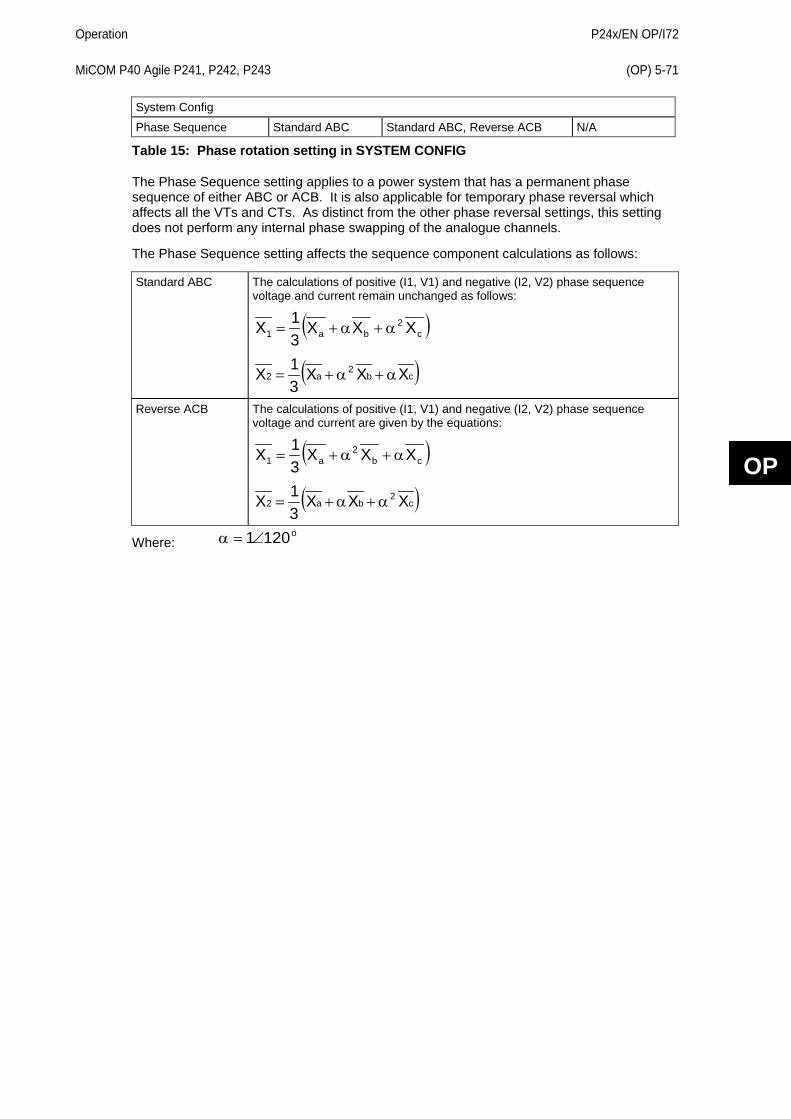
Operation
P24x/EN OP/I72 MiCOM P40 Agile P241, P242, P243 (OP) 5-71
OP
System Config
Phase Sequence Standard ABC Standard ABC, Reverse ACB N/A
Table 15: Phase rotation setting in SYSTEM CONFIG
The Phase Sequence setting applies to a power system that has a permanent phase sequence of either ABC or ACB. It is also applicable for temporary phase reversal which affects all the VTs and CTs. As distinct from the other phase reversal settings, this setting does not perform any internal phase swapping of the analogue channels.
The Phase Sequence setting affects the sequence component calculations as follows:
Standard ABC The calculations of positive (I1, V1) and negative (I2, V2) phase sequence voltage and current remain unchanged as follows:
( )c2
ba1 XXX31X α+α+=
( )cb2
a2 XXX31X α+α+=
Reverse ACB The calculations of positive (I1, V1) and negative (I2, V2) phase sequence
voltage and current are given by the equations:
( )cb2
a1 XXX31X α+α+=
( )c2
ba2 XXX31X α+α+=
Where: o1201∠=α

P24x/EN OP/I72
Operation (OP) 5-72 MiCOM P40 Agile P241, P242, P243
OP

Application Notes
P24x/EN AP/I72 MiCOM P40 Agile P241, P242, P243 (AP) 6-1
AP
APPLICATION NOTES

P24x/EN AP/I72
Application Notes (AP) 6-2 MiCOM P40 Agile P241, P242, P243
AP
Application Notes
P24x/EN AP/I72 MiCOM P40 Agile P241, P242, P243 (AP) 6-3
AP
CONTENTS
1 INTRODUCTION 9
1.1 Protection of asynchronous and synchronous motors 9
1.2 Introduction to the P24x relay 9
2 APPLICATION OF INDIVIDUAL PROTECTION FUNCTIONS 10
2.1 Motor differential protection (P243 only) (87) 10
2.1.1 Setting guidelines for biased differential protection 10
2.1.2 Setting guidelines for high impedance differential protection 11
2.1.3 Setting guidelines for the self balance winding differential 14
2.2 Thermal overload protection (49) 14
2.2.1 Introduction 14
2.2.2 Thermal replica 15
2.2.3 Setting guidelines for thermal overload 16
2.2.3.1 Thermal setting Ith 16
2.2.3.2 K coefficient 17
2.2.3.3 Thermal time constants 17
2.2.4 Thermal state modification 18
2.2.5 Thermal probe influence 20
2.2.6 Specific applications 20
2.2.6.1 Inhibition of the thermal trip during starting 20
2.2.6.2 Emergency restart 20
2.2.6.3 Thermal alarm 21
2.2.6.4 Lockout threshold 21
2.3 Resistive temperature detectors 21
2.3.1 RTD thermal protection features 21
2.3.2 RTD thermal protection settings 21
2.4 Short circuit protection (50/51) 22
2.4.1 Setting guidelines 23
2.4.2 Setting example 24
2.5 Earthfault protection (50N/51N/67N/32N/64N) 24
2.5.1 Solidly earthed system 26
2.5.1.1 Principle 26
2.5.1.2 Typical settings 27
2.5.2 Insulated system 28
2.5.2.1 Principle 28
2.5.2.2 Setting guidelines 30
2.5.3 Resistance earthed systems 30
2.5.3.1 Setting guidelines 30
2.5.3.2 High resistance earthing 30
P24x/EN AP/I72
Application Notes (AP) 6-4 MiCOM P40 Agile P241, P242, P243
AP
2.5.4 Petersen coil earthed systems 31
2.5.4.1 Principle 31
2.5.4.2 Operation of sensitive earth fault element 36
2.5.5 Wattmetric characteristic 37
2.5.5.1 Principle 37
2.5.5.2 Application considerations 38
2.5.5.3 Calculation of required relay settings: 38
2.6 Residual overvoltage (neutral displacement) protection (59N) 38
2.6.1 Setting guidelines 41
2.7 Negative sequence protection (46) 41
2.7.1 Loss of one phase while starting & running 43
2.7.1.1 Principle 43
2.7.1.2 Setting guidelines 44
2.7.2 3 Phase voltage check (reverse phase detection) (47/27) 44
2.7.2.1 Principle 44
2.7.2.2 Setting guidelines 44
2.8 Start / stall protection (48/51LR/50S/14) 44
2.8.1 Excessive start time/locked rotor protection - stall time > start time (51LR) 45
2.8.1.1 Setting guidelines 45
2.8.2 Stall protection (50S) 45
2.8.2.1 Principle 45
2.8.2.2 Setting guidelines 45
2.8.3 Excessive start time/locked rotor protection - stall time < start time (14) 46
2.8.3.1 Setting guidelines 46
2.8.4 Number of starts limitation (66) 46
2.8.5 Anti-Backspin protection (27 Abs) 47
2.8.6 Setting guidelines for ABS protection 47
2.8.7 Momentary reduction in system voltage during running of the motor 47
2.8.7.1 Low voltage protection (reacceleration authorization) 47
2.8.7.2 AUTO RE-START authorization: Re-start/load restoration 48
2.9 Undervoltage protection function (27) 48
2.9.1 Principle 48
2.9.2 Setting guidelines for undervoltage protection 49
2.10 Loss-of-load protection (37) 49
2.10.1 Principle 49
2.10.2 Setting guidelines 49
2.11 Synchronous motor protection 49
2.11.1 Out-of-step protection (under power factor) (55) 50
2.11.2 Reverse power (loss-of-supply) (32R) 50
2.11.2.1 Underfrequency (81U) 50
2.11.3 Setting guidelines: 50
2.11.3.1 Overvoltage (59) 50
Application Notes
P24x/EN AP/I72 MiCOM P40 Agile P241, P242, P243 (AP) 6-5
AP
2.11.3.2 Setting guidelines: 51
2.12 Field failure protection function (40) 51
2.12.1 Setting guidelines for field failure protection 51
2.12.1.1 Impedance element 1 51
2.12.1.2 Impedance element 2 52
2.12.1.3 Power factor element 53
2.13 Circuit breaker failure protection (50BF) 53
2.13.1 Breaker failure protection configurations 53
2.13.2 Reset mechanisms for breaker fail timers 53
2.13.3 Typical breaker fail timer settings 54
2.14 Current loop inputs and outputs 55
2.14.1 Current loop inputs 55
2.14.2 Setting guidelines for current loop inputs 55
2.14.3 Current loop outputs 55
2.14.4 Setting guidelines for current loop outputs 56
2.15 Phase rotation 56
3 APPLICATION OF NON-PROTECTION FUNCTIONS 58
3.1 VT supervision 58
3.1.1 Setting the VT supervision element 58
3.2 CT supervision 58
3.2.1 Setting the CT supervision element 59
3.3 Trip circuit supervision (TCS) 59
3.3.1 TCS scheme 1 59
3.3.1.1 Scheme description 59
3.3.2 Scheme 1 PSL 60
3.3.3 TCS scheme 2 60
3.3.3.1 Scheme description 60
3.3.4 Scheme 2 PSL 61
3.3.5 TCS scheme 3 61
3.3.5.1 Scheme description 61
3.3.6 Scheme 3 PSL 62
4 CURRENT TRANSFORMER REQUIREMENTS 63
4.1 Motor differential function (P243) 63
4.1.1 Biased differential protection 63
4.2 Non-directional definite time/IDMT short circuit and definite time/IDMT derived earth fault protection 64
4.2.1 Definite time/IDMT delayed short circuit elements 64
4.2.2 Definite time delayed/IDMT derived earth fault elements 64
4.3 Non-directional instantaneous short circuit and derived earth fault protection 64
4.3.1 Instantaneous short circuit elements 64
4.3.2 Instantaneous derived earth fault elements 64
4.4 Directional definite time/IDMT derived earth fault protection 65
P24x/EN AP/I72
Application Notes (AP) 6-6 MiCOM P40 Agile P241, P242, P243
AP
4.4.1 Directional time delayed derived earth fault protection 65
4.4.2 Directional instantaneous derived earth fault protection 65
4.5 Non-directional/directional definite time/IDMT sensitive earth fault (SEF) protection 65
4.5.1 Non-directional time delayed SEF protection (residually connected) 65
4.5.2 Non-directional instantaneous SEF protection (residually connected) 65
4.5.3 Directional time delayed SEF protection (residually connected) 65
4.5.4 Directional instantaneous SEF protection (residually connected) 65
4.5.5 SEF protection - as fed from a core-balance CT 65
4.6 Converting an IEC185 current transformer standard protection classification to a kneepoint voltage 66
4.7 Converting IEC185 current transformer standard protection classification to an ANSI/IEEE standard voltage rating 66
5 READ ONLY MODE 68
6 AUXILIARY SUPPLY FUSE RATING 69
FIGURES Figure 1: Example of settings 18
Figure 2: Thermal curve modification 19
Figure 3: OR logic 22
Figure 4: AND logic 23
Figure 5: Inhibition of V< and V2> during start 23
Figure 6: Definite time overcurrent element 23
Figure 7: Core balanced CT with cable 26
Figure 8: Fuse characteristic 27
Figure 9: Current distribution in an insulated system with C phase fault 28
Figure 10: Phasor diagrams for insulated system with C phase fault 29
Figure 11: Directional tripping characteristic 31
Figure 12: Current distribution in Petersen coil earthed system 32
Figure 13: Distribution of currents during a C phase to earth fault 33
Figure 14: Theoretical case - no resistance present in XL or XC 34
Figure 15: Zero sequence network showing residual currents 35
Figure 16: Practical case:- resistance present in XL and Xc 36
Figure 17: Resistive components of spill current 37
Figure 18: Residual voltage 40
Figure 19: Residual voltage 41
Figure 20: Equivalent circuits 42
Figure 21: TCS scheme 1 59
Figure 22: PSL for TCS schemes 1 and 3 60
Figure 23: TCS scheme 2 60
Figure 24: PSL for TCS scheme 2 61
Figure 25: TCS scheme 3 61
Application Notes
P24x/EN AP/I72 MiCOM P40 Agile P241, P242, P243 (AP) 6-7
AP
TABLES Table 1: Recommended characteristics and types of Metrosil units to be used with 1 Amp CTs 13
Table 2: Recommended characteristics and types of Metrosil units to be used with 5 Amp CTs 13
Table 3: Specific motor parameters used to show how to determine the P24x settings 16
Table 4: Reduction of per unit power delivered by motors relative to the ambient temperature 20
Table 5: Correction coefficients used by the relay to offset the thermal replica at different ambient temperatures 20
Table 6: Typical operating temperatures of a healthy plan 21
Table 7: Standard IDMT curve constant values 24
Table 8: CBF resetting options 54
Table 9: Typical CBF timer settings 54
Table 10: Recommended resistor value and opto voltage settings 60
Table 11: Recommended resistor value and opto voltage settings 62
Table 12: The CT requirements for the P24x protection functions excluding differential protection 63
Table 13: Auxiliary supplies and the corresponding fuse ratings 69

P24x/EN AP/I72
Application Notes (AP) 6-8 MiCOM P40 Agile P241, P242, P243
AP
Application Notes
P24x/EN AP/I72 MiCOM P40 Agile P241, P242, P243 (AP) 6-9
AP
1 INTRODUCTION
1.1 Protection of asynchronous and synchronous motors Both asynchronous (induction) and synchronous motors perform a vital role in many industrial processes throughout the world, a vast majority of which would be unable to function without such a device. Loss of a motor through damage incurs much more than a possible electrical rewind but also a stop in an electrical process, resulting in expensive plant down time. This problem may be exacerbated by the damaged machine being positioned in an inaccessible position, such as an awkward corner of a factory or by a spare not being readily available. Therefore, prior warning of a problem is vitally important to reduce the impact on a process resulting from a faulted motor.
Comprehensive protection relays, such as the P24x, can be used to protect a motor from catastrophic failure, or possibly give the operator prior warning of a problem, which can reduce plant down time. Any protective device, though reliable in operation under abnormal conditions, must not affect the continuous operation of the motor under normal operating conditions.
Unfortunately, motor characteristics vary greatly depending on their precise application. Each application requires careful consideration regarding the specification and setting of the motor protection. For example, starting and stalling currents and times must be known when applying overload protection, and furthermore the thermal withstand of the machine under balanced and unbalanced loading must be defined.
The conditions which motor protection detects can be divided into two broad categories; imposed external conditions and internal faults. Imposed external conditions include unbalanced supply voltages, undervoltages, single phasing and reverse phase sequence starting and in synchronous machines only, loss of synchronism. Internal faults include bearing failures, internal shunt faults (commonly earth faults), and overloads.
1.2 Introduction to the P24x relay The MiCOM Px40 relay range uses the latest numerical technology and includes devices designed for the protection of a wide range of power system plant such as motors, generators, feeders, overhead lines and cables.
These relays are designed around a common hardware and software platform to achieve a high degree of commonality between products. One such product in the range is the Motor Protection Relay. This relay has been designed to cater for the protection of both asynchronous and synchronous motors, which may require extensive protection.
The relay also includes a comprehensive range of non-protection features to aid with power system diagnosis and fault analysis. All these features can be accessed remotely from one of the relays remote, serial communications options.

P24x/EN AP/I72
Application Notes (AP) 6-10 MiCOM P40 Agile P241, P242, P243
AP
2 APPLICATION OF INDIVIDUAL PROTECTION FUNCTIONS The following sections detail the individual protection functions in addition to where and how they may be applied.
2.1 Motor differential protection (P243 only) (87) Failure of stator windings or connection insulation can result in severe damage to the windings and the stator core. The extent of the damage depends on the fault current level and the duration of the fault. Protection should be applied to limit the damage and repair costs.
The MiCOM P243 provides motor differential protection. This form of unit protection allows discriminative detection of winding faults. It has no intentional time delay where a significant fault current arises. Arrange the protection zone, defined by the location of the CTs, to overlap protection for other items of plant, such as a busbar or transformer.
Heavy through current arising from an external fault condition can cause one CT to saturate more than the other. This results in a difference between the secondary current produced by each CT. It is essential to stabilize the protection for these conditions. Three methods are commonly used:
• A biasing technique, where the relay setting is raised as through-current increases.
• A high impedance technique, where the relay impedance is such that under maximum through-fault conditions, the current in the differential element is insufficient for the relay to operate.
• A self balance type differential protection arrangement.
Note: If the conductors are placed reasonably concentric within the window of the core balance current transformers, spill current can be kept to a minimum. With this low spill current and a reasonably independence of CT ratio to full load a lower fault setting could be achieved than conventional high impedance circulating current differential schemes.
The motor differential protection function available in the P24x relay can be used in either biased differential or high impedance differential mode.
Note: The high impedance mode can be used to achieve a self balance scheme. Both modes of operation are equally valid; users may have a preference for one over the other. The operating principle of each is described in the Operation chapter, P24x/EN OP.
2.1.1 Setting guidelines for biased differential protection To select biased differential protection, set the Diff Function cell to Percentage Bias.
Set the differential current setting Diff Ιs1 to a low setting to protect as much of the machine winding as possible. A setting of 5% of rated current of the machine is generally considered to be adequate. Set Diff Ιs2, the threshold above which the second bias setting is applied, to 120% of the machine rated current.
Set the initial bias slope setting, Diff k1 to 0% to provide optimum sensitivity for internal faults. Set the second bias slope, Diff k2 to 150% to provide adequate stability for external faults.
These settings can be increased where low accuracy class CTs are used to supply the protection.

Application Notes
P24x/EN AP/I72 MiCOM P40 Agile P241, P242, P243 (AP) 6-11
AP
2.1.2 Setting guidelines for high impedance differential protection Set the Diff Function cell to High Impedance to select high impedance differential protection.
Set the differential current setting Diff Ιs1 to a low setting to protect as much of the machine winding as possible. A setting of 5% of rated current of the machine is adequate. This setting may need to be increased where low accuracy class CTs are used to supply the protection. Make sure the primary operating current of the element is less than the minimum fault current for which the protection should operate.
The primary operating current (Ιop) is a function of the current transformer ratio, the relay operating current (Diff Ιs1), the number of current transformers in parallel with a relay element (n) and the magnetizing current of each current transformer (Ιe) at the stability voltage (Vs). This relationship can be expressed in three ways:
To determine the maximum current transformer magnetizing current to achieve a specific primary operating current with a particular relay operating current.
>−×< 1..
.1
SOP
e IREFDiffMotRatioCT
In
I
To determine the maximum relay current setting to achieve a specific primary operating current with a given current transformer magnetizing current.
−< e
OPS nI
RatioCTIIDiffMot.
1..
To express the protection primary operating current for a particular relay operating current and with a particular level of magnetizing current.
( ) ( )eSOP nIIDiffMotRatioCTI +×= 1...
To achieve the required primary operating current with the current transformers that are used, a current setting (Diff Ιs1) must be selected for the high impedance element, as detailed in expression (ii) above. The setting of the stabilizing resistor (RST) must be calculated in the following manner, where the setting is a function of the required stability voltage setting (Vs) and the relay current setting (Diff Ιs1).
( )1..25.1........
1.. S
CTF
S
SST IDiffMot
RLRIIDiffMot
VR +××==
Note: The above formula assumes negligible relay burden.
USE OF “METROSIL” NON-LINEAR RESISTORS
Metrosils are used to limit the peak voltage developed by the current transformers under internal fault conditions, to a value below the insulation level of the current transformers, relay and interconnecting leads, which are normally able to withstand 3000 V peak.
Use the following formulae to estimate the peak transient voltage produced for an internal fault. This is a function of the current transformer kneepoint voltage and the prospective voltage that would be produced for an internal fault if current transformer saturation did not occur. This prospective voltage is a function of maximum internal fault secondary current, the current transformer ratio, the current transformer secondary winding resistance, the current transformer lead resistance to the common point, the relay lead resistance and the stabilizing resistor value.
Vp = 2 2Vk ( ) Vf - Vk
Vf = Ι'f (RCT + 2RL + RST)
Where:
Vp = Peak voltage developed by the CT under internal fault conditions.

P24x/EN AP/I72
Application Notes (AP) 6-12 MiCOM P40 Agile P241, P242, P243
AP
Vk = Current transformer knee-point voltage.
Vf = Maximum voltage that would be produced if CT saturation did not occur.
Ι‘f = Maximum internal secondary fault current.
RCT = Current transformer secondary winding resistance.
RL = Maximum lead burden from current transformer to relay.
RST = Relay stabilizing resistor.
When the value given by the formulae is greater than 3000 V peak, Metrosils should be applied. They are connected across the relay circuit and serve the purpose of shunting the secondary current output of the current transformer from the relay to prevent very high secondary voltages.
Metrosils are externally mounted and take the form of annular discs. Their operating characteristics follow the expression:
V = CΙ 0.25
Where:
V = Instantaneous voltage applied to the non-linear resistor (“Metrosil”).
C = Constant of the non-linear resistor (“Metrosil”).
Ι = Instantaneous current through the non-linear resistor (“Metrosil”).
With a sinusoidal voltage applied across the Metrosil, the RMS current would be approximately 0.52x the peak current. This current value can be calculated as follows:
Ι(rms) = 0.52
Vs (rms) x 2
C 4
Where:
Vs(rms) = rms value of the sinusoidal voltage applied across the Metrosil.
This is due to the fact that the current waveform through the non-linear resistor (“Metrosil”) is not sinusoidal but appreciably distorted.
For satisfactory application of a non-linear resistor (“Metrosil”), its characteristic should comply with the following requirements:
• At the relay voltage setting, the non-linear resistor (“Metrosil”) current should be as low as possible, but no greater than approximately 30 mA rms. for 1 A current transformer and approximately 100 mA rms. for 5 A current transformers.
• At the maximum secondary current, the non-linear resistor (“Metrosil”) should limit the voltage to 1500 V rms or 2120 V peak for 0.25 second. At higher relay voltage settings, it is not always possible to limit the fault voltage to 1500 V rms., so higher fault voltages may have to be tolerated.
The following tables show the typical Metrosil types that are required, depending on relay current rating, REF voltage setting etc.
Metrosil Units for Relays with a 1 Amp CT
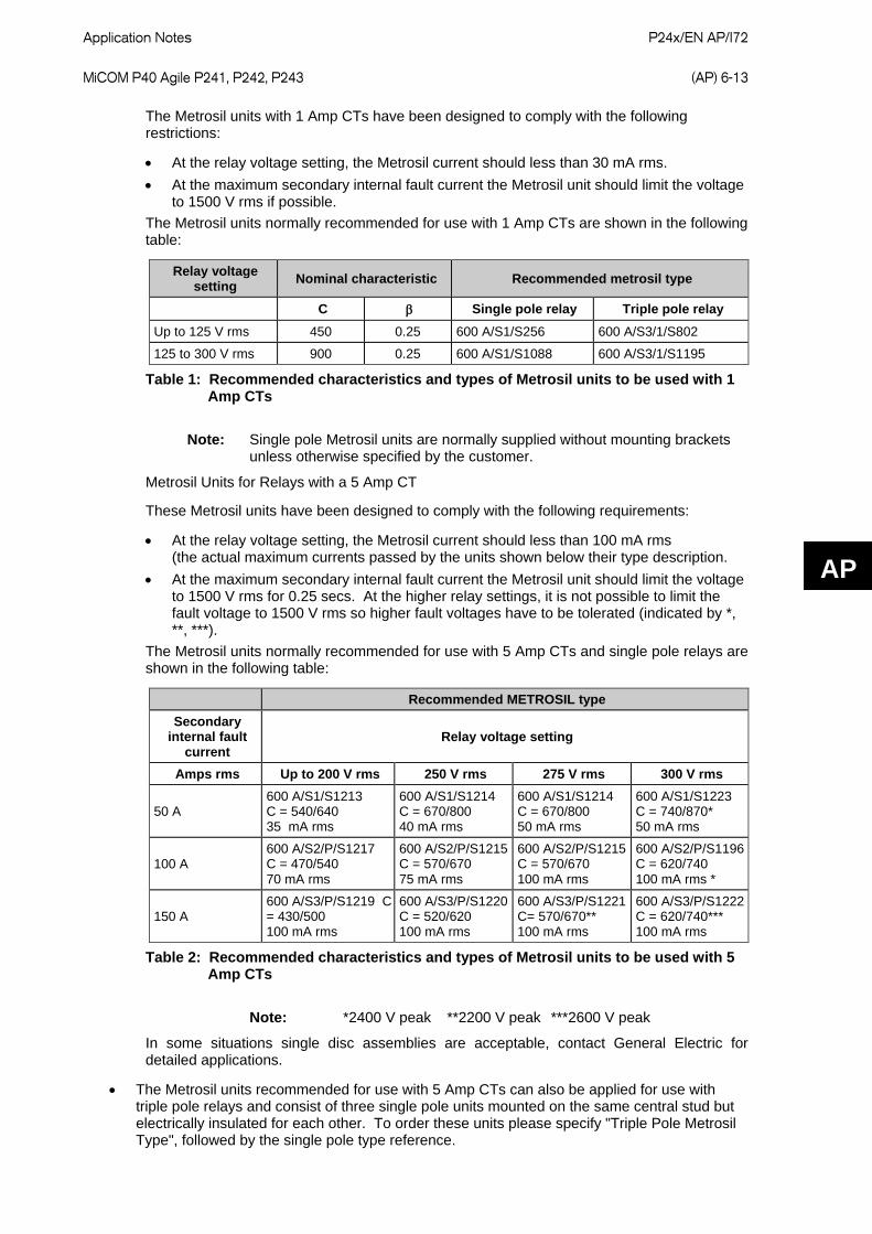
Application Notes
P24x/EN AP/I72 MiCOM P40 Agile P241, P242, P243 (AP) 6-13
AP
The Metrosil units with 1 Amp CTs have been designed to comply with the following restrictions:
• At the relay voltage setting, the Metrosil current should less than 30 mA rms. • At the maximum secondary internal fault current the Metrosil unit should limit the voltage
to 1500 V rms if possible. The Metrosil units normally recommended for use with 1 Amp CTs are shown in the following table:
Relay voltage setting Nominal characteristic Recommended metrosil type
C β Single pole relay Triple pole relay Up to 125 V rms 450 0.25 600 A/S1/S256 600 A/S3/1/S802
125 to 300 V rms 900 0.25 600 A/S1/S1088 600 A/S3/1/S1195
Table 1: Recommended characteristics and types of Metrosil units to be used with 1 Amp CTs
Note: Single pole Metrosil units are normally supplied without mounting brackets unless otherwise specified by the customer.
Metrosil Units for Relays with a 5 Amp CT
These Metrosil units have been designed to comply with the following requirements:
• At the relay voltage setting, the Metrosil current should less than 100 mA rms (the actual maximum currents passed by the units shown below their type description.
• At the maximum secondary internal fault current the Metrosil unit should limit the voltage to 1500 V rms for 0.25 secs. At the higher relay settings, it is not possible to limit the fault voltage to 1500 V rms so higher fault voltages have to be tolerated (indicated by *, **, ***).
The Metrosil units normally recommended for use with 5 Amp CTs and single pole relays are shown in the following table:
Recommended METROSIL type Secondary
internal fault current
Relay voltage setting
Amps rms Up to 200 V rms 250 V rms 275 V rms 300 V rms
50 A 600 A/S1/S1213 C = 540/640 35 mA rms
600 A/S1/S1214 C = 670/800 40 mA rms
600 A/S1/S1214 C = 670/800 50 mA rms
600 A/S1/S1223 C = 740/870* 50 mA rms
100 A 600 A/S2/P/S1217 C = 470/540 70 mA rms
600 A/S2/P/S1215 C = 570/670 75 mA rms
600 A/S2/P/S1215 C = 570/670 100 mA rms
600 A/S2/P/S1196 C = 620/740 100 mA rms *
150 A 600 A/S3/P/S1219 C = 430/500 100 mA rms
600 A/S3/P/S1220 C = 520/620 100 mA rms
600 A/S3/P/S1221 C= 570/670** 100 mA rms
600 A/S3/P/S1222 C = 620/740*** 100 mA rms
Table 2: Recommended characteristics and types of Metrosil units to be used with 5 Amp CTs
Note: *2400 V peak **2200 V peak ***2600 V peak
In some situations single disc assemblies are acceptable, contact General Electric for detailed applications.
• The Metrosil units recommended for use with 5 Amp CTs can also be applied for use with triple pole relays and consist of three single pole units mounted on the same central stud but electrically insulated for each other. To order these units please specify "Triple Pole Metrosil Type", followed by the single pole type reference.
P24x/EN AP/I72
Application Notes (AP) 6-14 MiCOM P40 Agile P241, P242, P243
AP
• Metrosil units for higher relay voltage settings and fault currents can be supplied if required. For further advice and guidance on selecting METROSILS please contact the Applications department at General Electric.
2.1.3 Setting guidelines for the self balance winding differential For this configuration, the relay must be set to High Impedance using the cell Diff Function in the Differential protection menu. Set the differential current setting Diff Ιs1 to a low setting to protect as much of the machine winding as possible. A setting of 5% of rated current of the machine is generally considered adequate.
If the conductors are placed reasonably concentrically within the window of the core balance current transformers, spill current can be kept to a minimum. This low spill current and a reasonable independence of CT ratio to full load, allows a lower fault setting than with conventional high impedance circulating current differential schemes.
Disadvantages:
1. The necessity of passing both ends of each phase winding through the CT and so the need for extra cabling on the neutral end.
2. To avoid long cabling, position of CTs are restricted to the proximity of the machine output terminals in which case the cable between the machine output terminals and controlling switchgear might not be included within the differential zone.
2.2 Thermal overload protection (49) For the Thermal overload protection function to operate correctly, the circuit breaker must be closed and its associated closing signal, 52a, must be recognized by the relay.
2.2.1 Introduction Overloads can result in stator temperature rises which exceed the thermal limit of the winding insulation. Empirical results suggest that the life of insulation is approximately halved for each 10°C rise in temperature above the rated value. The life of insulation is not wholly dependent on the rise in temperature but on the time the insulation is maintained at this elevated temperature. Due to the relatively large heat storage capacity of an induction motor, infrequent overloads of short duration may not damage the machine. However, sustained overloads of a few per cent may result in premature ageing and failure of insulation.
The physical and electrical complexity of motor construction, their diverse applications, variety of possible abnormal operating conditions and the different modes of failure that may occur, result in a complex thermal relationship. It is not therefore possible to create an accurate mathematical model of the true thermal characteristics of the machine.
However, if a motor is considered to be a homogeneous body, developing heat internally at a constant rate and dissipating heat at a rate directly proportional to its temperature rise, it can be shown that the temperature at any instant is given by;
T = Tmax (1 – e -t/τ)
Where;
Tmax = Final steady state temperature,
τ = Heating time constant.
This assumes a thermal equilibrium in the form:
Heat developed = Heat stored + Heat dissipated
Temperature rise is proportional to the current squared:
T = KIR2 (1 – e -t/τ)
Where;
IR = That current, which when left to flow continuously, would produce a temperature Tmax, in the motor.
Application Notes
P24x/EN AP/I72 MiCOM P40 Agile P241, P242, P243 (AP) 6-15
AP
For an overload current 'I', the temperature is given by;
T = KI2 (1 – e -t/τ)
For a motor not to exceed the rated temperature, the time 't' for which the motor can withstand the current 'I' can be shown to be given by;
t = τ Ln [1/1-(IR/I)2]
An overload protection element should therefore satisfy the above relationship. The value of IR may be the full load motor current or a percentage of it, depending on the motor design.
It is an oversimplification to regard a motor as a homogeneous body. The temperature rise of different parts, or even of various points in the same part, can be very uneven. However, it is reasonable to consider the current-time relationship follows an inverse fashion. A more accurate representation of the thermal state of the motor can be obtained through the use of temperature monitoring devices (RTDs) which target these specific areas.
2.2.2 Thermal replica The P24x relay models the time-current thermal characteristic of a motor by internally generating a thermal replica of the machine. The thermal overload protection can be selectively enabled or disabled. The positive or rms and negative sequence components of the load current are measured independently and are combined together to form an equivalent current, Ieq, which is supplied to this replica circuit. The heating effect in the thermal replica is produced by Ieq2 and therefore takes into account the heating effect due to both positive or rms and negative sequence components of current.
The equivalent current for operation of the overload protection is in accordance with the following expressions;
Ieq = √(I12 + KI22)
Note: This equation is used in software version A4.x (09) and before
Ieq = √(IRMS2 + KI22)
Note: This equation is used in software version B1.0 (20) and later
Where;
IRMS = Root Mean Square current
I1 = Positive sequence current
I2 = Negative sequence current
K = A user settable constant proportional to the thermal capacity of the motor.
As previously described, the temperature of a motor rises exponentially with increasing current. Similarly, when current decreases, the temperature also decreases in a similar manner. Therefore, to achieve close sustained overload protection, the P24x relay incorporates a wide range of thermal time constants. These allow the relay replica to closely match the protected motor during heating and cooling.
Furthermore, the thermal withstand capability of the motor is affected by heating in the winding prior to the fault. The thermal replica is designed to take into account the extremes of zero pre-fault current, known as the 'cold' condition, and full rated pre-fault current, known as the 'hot' condition. With no pre-fault current, the relay operates on the 'cold curve'. When a motor is, or has been, running at full load prior to a fault, the windings dissipate heat and the 'hot curve' is applicable. Therefore, during normal operation, the relay operates in these two limits, unless programmed to do otherwise.
To protect the motor during all operating conditions, three independently adjustable time constants are employed in the overload curve:
• T1 = Overload time constant applied when the current is between Ith & 2Ith.
• T2 = Overload time constant applied for currents above 2Ith.
P24x/EN AP/I72
Application Notes (AP) 6-16 MiCOM P40 Agile P241, P242, P243
AP
• Tr = Cooling time constant applied when the motor is stopped.
The following equation is used to calculate the trip time for a given current.
Note: The relay trips at a value corresponding to 100% of its thermal state. The percentage of thermal capacity follows the relationship %θ = ( Ieq/Ith)2 x 100.
t = T Ln [(k2 - A2)/(k2 - 1)]
And the following equation is used to calculate the time it takes for the thermal alarm to be set.
talarm = T Ln [(k2 – A2)/(k2 – (Thermal Alarm/100))]
Where;
T = T1 if Ith < Ieq <= 2Ith
T = T2 if Ieq > 2Ith
T = Tr if Ieq = 0 (CB open)
k = Ieq/Ith
A = initial thermal state of the machine.
Ith = Thermal current setting
Thermal Alarm = Thermal alarm setting (20%-100%)
The time to trip varies depending on the load current carried before application of the overload, such as whether the overload was applied from “hot” or “cold”.
2.2.3 Setting guidelines for thermal overload
2.2.3.1 Thermal setting Ith The Ith Current Set setting chosen depends on the type of motor being protected. Most machines are termed CMR (continuous maximum rating) motors. These motors are designed to carry the nameplate value or full load current continuously. A CMR motor may be run at some value less than its CMR and set to trip at its CMR.
Alternatively, if the machine is not a CMR motor, then the Ith setting needs to take into account the amount of overload, which can be tolerated, without resulting in thermal damage. A typical allowable overload may be in the region of 10% of rated temperature. It is important to realize that the temperature build up in the machine is approximately equal to the current squared; therefore a 10% temperature overload is equivalent to a 5% current overload.
Setting example:
The following motor parameters are used to show how to determine the P24x settings;
Voltage 11 kV Full load current 293 A
Starting current 470 %
Starting time 10 s
Heating time constant 20 min
Cooling time constant 100 min
Hot locked rotor withstand time 20 s
Cold locked rotor withstand time 30 s
CT Ratio 300 / 1
VT Ratio 11.5 kV / 110 V
Starting D.O.L
Table 3: Specific motor parameters used to show how to determine the P24x settings

Application Notes
P24x/EN AP/I72 MiCOM P40 Agile P241, P242, P243 (AP) 6-17
AP
1 300
For this application we have assumed the machine is a CMR motor and therefore the Ith
setting is calculated as follows;
Ith = ICMR x (1/CT Ratio)
Where:
ICMR = Continuous Motor Rating
Therefore: Ith = 293 x = 0.976 In
Therefore set: Ith = 0.98 In
2.2.3.2 K coefficient The constant K Coefficient is used to increase the influence of negative sequence current on the thermal replica. This factor should be set equal to the ratio of negative phase sequence, rotor resistance to positive sequence resistance at rated speed. When an exact setting cannot be calculated, a default setting of 3 should be used. This is a typical setting and is sufficient for the majority of applications.
Therefore set: K Coefficient = 3
2.2.3.3 Thermal time constants The relay heating and cooling time constants are set in accordance with the stator thermal heating and cooling time constants. The relay heating time constant (Thermal Const T1) should be set equal to, or as close as possible to, the stator heating thermal time constant, which is obtainable from the motor manufacturer. It is good practice to set T1 slightly less than the stator heating thermal time constant to allow for relay tolerances. However, this is not always necessary, since the stator thermal time constants provided by the motor manufacturer are usually conservative.
Thermal Const T2 is automatically applied above 2 Ith and is used to modify the relay thermal curve during starting for certain applications, for example, where star/delta starters are being utilized. During normal running, with the motor connected in delta, the current in the motor winding is only 57% of that monitored by the relay. However, during starting, with the motor connected in star, the current monitored by the relay is equal to the current in the motor winding. For this reason, T2 can be used to reduce the operating time of the relay during starting. For applications where direct on line (DOL) starting is utilized, T2 should be set equal to T1, resulting in one continuous thermal curve.
It is important to plot the chosen thermal characteristics on a time-current graph to ensure that the cold curve does not intersect the starting characteristic.
In certain applications, the thermal time constants may not be available. However, a graphical representation of these values may be given. In such applications, a stator heating time constant must be chosen, such that when plotted on a time-current graph, it closely matches the cold withstand curve of the motor.
Cooling Const Tr is the cooling time constant. This setting is important for cyclic operation of the motor, since precise information of the thermal state of the motor is required during heating and cooling. It is set as a multiple of T1 and should be set to the nearest value above the motor cooling time constant.
Setting Example:
For this particular application the stator thermal time constants of the motor are known, therefore the required time constant settings are as follows;
Therefore set: T1 = 20 minutes
T2 = T1 since machine is DOL starting
Tr to 5 x T1 = 100 mins. These settings are shown in Figure 1.
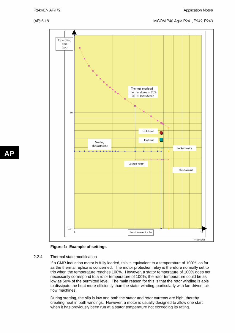
P24x/EN AP/I72
Application Notes (AP) 6-18 MiCOM P40 Agile P241, P242, P243
AP
Figure 1: Example of settings
2.2.4 Thermal state modification If a CMR induction motor is fully loaded, this is equivalent to a temperature of 100%, as far as the thermal replica is concerned. The motor protection relay is therefore normally set to trip when the temperature reaches 100%. However, a stator temperature of 100% does not necessarily correspond to a rotor temperature of 100%; the rotor temperature could be as low as 50% of the permitted level. The main reason for this is that the rotor winding is able to dissipate the heat more efficiently than the stator winding, particularly with fan-driven, air-flow machines.
During starting, the slip is low and both the stator and rotor currents are high, thereby creating heat in both windings. However, a motor is usually designed to allow one start when it has previously been run at a stator temperature not exceeding its rating.
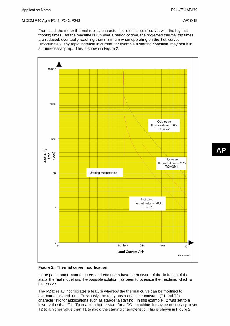
Application Notes
P24x/EN AP/I72 MiCOM P40 Agile P241, P242, P243 (AP) 6-19
AP
From cold, the motor thermal replica characteristic is on its 'cold' curve, with the highest tripping times. As the machine is run over a period of time, the projected thermal trip times are reduced, eventually reaching their minimum when operating on the 'hot' curve. Unfortunately, any rapid increase in current, for example a starting condition, may result in an unnecessary trip. This is shown in Figure 2.
Figure 2: Thermal curve modification
In the past, motor manufacturers and end users have been aware of the limitation of the stator thermal model and the possible solution has been to oversize the machine, which is expensive.
The P24x relay incorporates a feature whereby the thermal curve can be modified to overcome this problem. Previously, the relay has a dual time constant (T1 and T2) characteristic for applications such as star/delta starting. In this example T2 was set to a lower value than T1. To enable a hot re-start, for a DOL machine, it may be necessary to set T2 to a higher value than T1 to avoid the starting characteristic. This is shown in Figure 2.

P24x/EN AP/I72
Application Notes (AP) 6-20 MiCOM P40 Agile P241, P242, P243
AP
2.2.5 Thermal probe influence Motors are designed to operate within a specific ambient temperature. If the machine is operated in a higher ambient temperature than specified, the windings may overheat resulting in insulation deterioration, even if it is operating within rated load. Therefore, if the machine is operated in an environment where the ambient temperature may fluctuate, it is important to compensate the thermal overload curve to maintain close thermal overload protection. Strategically placed temperature sensors can be used to provide information on ambient conditions, which in turn can then be used to influence the thermal replica. Motors which are particularly at risk are those operated in direct sunlight, boiler houses, tropical environments and motors which are reliant on forced cooling.
The power delivered by a motor varies with the ambient temperature, the following table shows variations in power delivered as the temperature changes for a typical motor.
Ambient Temperature °C 40 45 50 55 60 Power delivered as a % of nominal power
100 95 90 85 80
Table 4: Reduction of per unit power delivered by motors relative to the ambient temperature
As the nominal power varies linearly with nominal current, with a constant voltage, the above table is applicable to nominal current.
The thermal setting is also directly proportional to nominal current. So to compensate for the ambient temperature variation, the thermal setting is corrected dependent on the ambient temperature for the following conditions:
• During the calculation of thermal state • During the detection of thermal alarm • During the detection of thermal overload • During the detection of thermal lockout A correction coefficient is calculated depending on the temperature as shown in the table below and is multiplied to the thermal thresholds:
Ambient Temperature °C 40 45 50 55 60 65 Multiplication Coefficient 1 0.95 0.90 0.85 0.80 0.75
Table 5: Correction coefficients used by the relay to offset the thermal replica at different ambient temperatures
The P24x accepts inputs from up to 10 RTDs (resistance temperature detectors). Two of these RTDs (one main and one back-up), can be used to measure the external/ambient temperature and influences the thermal curve.
2.2.6 Specific applications
2.2.6.1 Inhibition of the thermal trip during starting It may be necessary to disable the thermal overload curve when starting motors which have extreme starting conditions, such as very long start times or very high start current values. With this feature enabled, if the calculated thermal state reaches 90% before the end of the starting period, this value is retained at 90% for the remaining starting period. At the end of the starting period the inhibit is removed.
Note: This function does not affect the operation of the Thermal Alarm feature.
2.2.6.2 Emergency restart Where a motor forms part of an essential process, it is sometimes desirable for it to continue operation, even under severe overload conditions. This usually means the motor being subjected to temperatures in excess of its design limits. Even though this may decrease the life of the motor, or even under extreme circumstances, burn the motor out, this may be justified for the application.

Application Notes
P24x/EN AP/I72 MiCOM P40 Agile P241, P242, P243 (AP) 6-21
AP
2.2.6.3 Thermal alarm The Thermal Alarm threshold is expressed as a percentage of the thermal state of the machine and is used to give an alarm when the thermal state reaches a predetermined value. There is no definitive setting for the thermal alarm threshold since it is application dependent. A typical setting would be 90%
2.2.6.4 Lockout threshold This facility can be used to inhibit a hot restart until the motor has cooled to the Lockout Thresh. This setting is expressed as a percentage of the thermal state of the motor. A contact is designed to open when the thermal state of the machine reaches this setting and close again when the thermal state drops below this setting. This contact would therefore be wired into the starting circuitry to provide the inhibit.
There is no definitive setting for the lockout threshold since it is based on the motors capability to withstand a hot restart. It is typically set to the minimum value of 20%Ith.
2.3 Resistive temperature detectors Prolonged overloading of motors or generators can cause their windings to overheat, resulting in premature ageing of the insulation, or in extreme cases, insulation failure. Worn or unlubricated bearings can also generate localized heating within the bearing housing. To protect against any general or localized overheating, the P24x relays have the ability to accept inputs from resistive temperature sensing devices (RTDs). Such probes are strategically placed in areas of the machine which are susceptible to overheating, or heat damage.
2.3.1 RTD thermal protection features Typically an RTD probe can measure temperature within the range -40 to +400°C. The temperature at each probe location can be determined by the relay, and is available for:
• Temperature monitoring, displayed locally, or remotely via the relay communications • Alarming, should a temperature threshold be exceeded for longer than a set time delay • Tripping, should a temperature threshold be exceeded for longer than a set time delay • Should the measured resistance be outside of the permitted range, an RTD failure alarm
is raised, indicating an open or short circuit RTD input
Note: Direct temperature measurement can provide more reliable thermal protection than devices which use a thermal replica energized from phase current. The latter is susceptible to inaccuracies in time constants used by the replica model, and also inaccuracies due to the variation in ambient temperature.
2.3.2 RTD thermal protection settings Typical operating temperatures for protected plant are given. Actual figures must be obtained from the equipment manufacturers:
Parameter Typical service temperature at full load
Short term overloading
Bearing temperature of motors or generators
Possibly 60 – 80°C, depending on the type of bearing.
+60 - +80°C
Top oil temperature of transformers 80°C (50 – 60°C above ambient). A temperature gradient from winding temperature is usually assumed, such that top oil RTDs can provide winding protection.
Winding hot spot temperature 98°C for normal ageing of insulation. Cyclic overloading might give +140°C during emergencies.
Table 6: Typical operating temperatures of a healthy plan
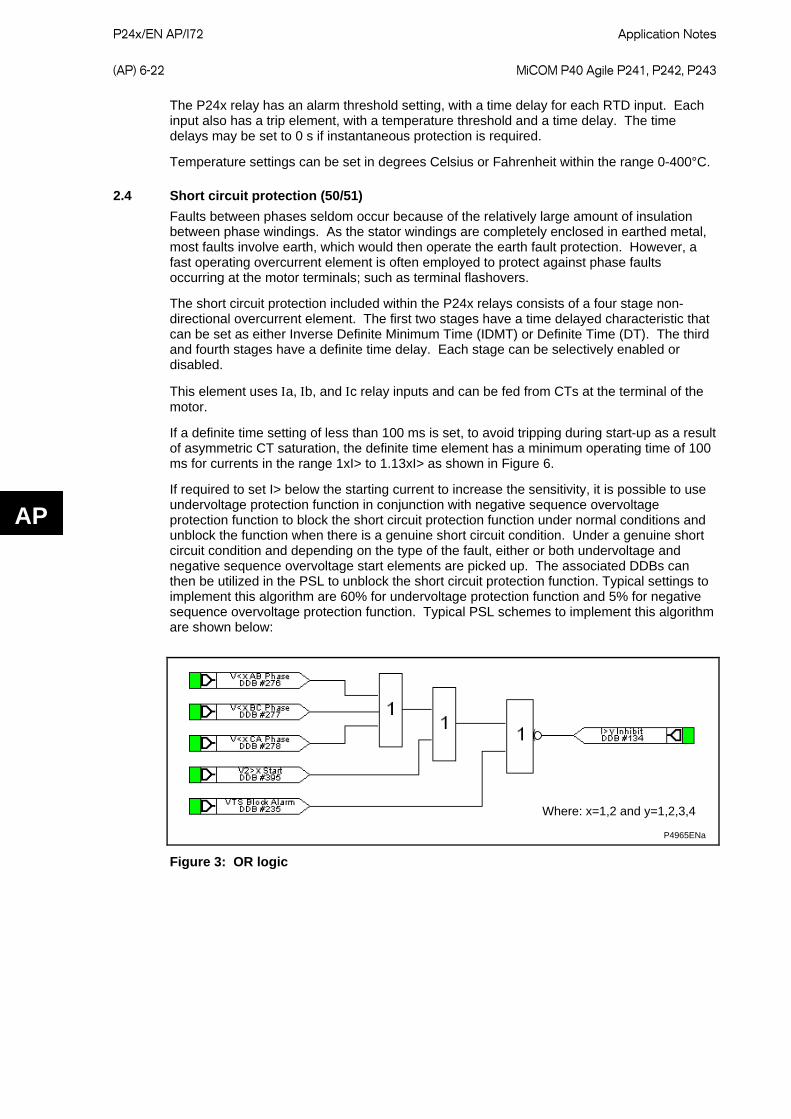
P24x/EN AP/I72
Application Notes (AP) 6-22 MiCOM P40 Agile P241, P242, P243
AP
The P24x relay has an alarm threshold setting, with a time delay for each RTD input. Each input also has a trip element, with a temperature threshold and a time delay. The time delays may be set to 0 s if instantaneous protection is required.
Temperature settings can be set in degrees Celsius or Fahrenheit within the range 0-400°C.
2.4 Short circuit protection (50/51) Faults between phases seldom occur because of the relatively large amount of insulation between phase windings. As the stator windings are completely enclosed in earthed metal, most faults involve earth, which would then operate the earth fault protection. However, a fast operating overcurrent element is often employed to protect against phase faults occurring at the motor terminals; such as terminal flashovers.
The short circuit protection included within the P24x relays consists of a four stage non-directional overcurrent element. The first two stages have a time delayed characteristic that can be set as either Inverse Definite Minimum Time (IDMT) or Definite Time (DT). The third and fourth stages have a definite time delay. Each stage can be selectively enabled or disabled.
This element uses Ιa, Ιb, and Ιc relay inputs and can be fed from CTs at the terminal of the motor.
If a definite time setting of less than 100 ms is set, to avoid tripping during start-up as a result of asymmetric CT saturation, the definite time element has a minimum operating time of 100 ms for currents in the range 1xI> to 1.13xI> as shown in Figure 6.
If required to set I> below the starting current to increase the sensitivity, it is possible to use undervoltage protection function in conjunction with negative sequence overvoltage protection function to block the short circuit protection function under normal conditions and unblock the function when there is a genuine short circuit condition. Under a genuine short circuit condition and depending on the type of the fault, either or both undervoltage and negative sequence overvoltage start elements are picked up. The associated DDBs can then be utilized in the PSL to unblock the short circuit protection function. Typical settings to implement this algorithm are 60% for undervoltage protection function and 5% for negative sequence overvoltage protection function. Typical PSL schemes to implement this algorithm are shown below:
Where: x=1,2 and y=1,2,3,4
P4965ENa
Figure 3: OR logic
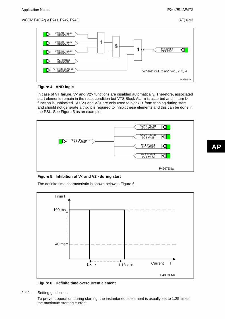
Application Notes
P24x/EN AP/I72 MiCOM P40 Agile P241, P242, P243 (AP) 6-23
AP
Where: x=1, 2 and y=1, 2, 3, 4
P4966ENa
Figure 4: AND logic
In case of VT failure, V< and V2> functions are disabled automatically. Therefore, associated start elements remain in the reset condition but VTS Block Alarm is asserted and in turn I> function is unblocked. As V< and V2> are only used to block I> from tripping during start and should not generate a trip, it is required to inhibit these elements and this can be done in the PSL. See Figure 5 as an example.
P4967ENa
Figure 5: Inhibition of V< and V2> during start
The definite time characteristic is shown below in Figure 6.
P4083ENb
Time t
100 ms
1 x I> 1.13 x I> Current I
40 ms
Figure 6: Definite time overcurrent element
2.4.1 Setting guidelines To prevent operation during starting, the instantaneous element is usually set to 1.25 times the maximum starting current.
P24x/EN AP/I72
Application Notes (AP) 6-24 MiCOM P40 Agile P241, P242, P243
AP
The timer setting is very much system dependent, but may typically be set to a value in the region of 100 ms. A time delay setting of less than 2 cycles duration is not realistic due to the fact that a minimum confirmation time, equivalent to two cycle duration, is required before tripping.
Note: If the motor is controlled by a fused contactor, it needs to be coordinated with the fuse. This is to prevent the contactor attempting to interrupt current in excess of its breaking capacity.
2.4.2 Setting example Utilizing the previously specified motor parameters, set:
I>Current Set = (1.25 x 4.7 x 293)/300 = 5.7 In I> Time Delay = 100 ms These settings are shown in Figure 6.
2.5 Earthfault protection (50N/51N/67N/32N/64N) One of the most common faults on a motor is a stator winding fault. This is usually the result of prolonged or cyclic overheating, which causes the insulation to deteriorate. Since the windings are surrounded by an earthed metal case, stator faults usually manifest themselves as earthfaults. The type of earthfault protection and CT arrangement adopted depends on the amount of earth fault current available during a fault. The magnitude of current is dependent on the system earthing arrangements.
The P24x earth fault element is equipped with two independent stages, which are selectable as either forward, reverse or non-directional. The first stage may be selected as either IDMT or DT and the second stage is DT only.
The inverse time delayed characteristics listed above, comply with the following formula:
t = T x [ K / ((I/Is)α ( - 1)) ] + L
Where;
t = operation time
K =constant I = measured current
Is = current threshold setting
α = constant
L = ANSI/IEEE constant (zero for IEC curves)
T = Time multiplier Setting or Time Dial Setting
Curve description Standard K constant α constant L constant
Standard Inverse IEC 0.14 0.02 0
Very Inverse IEC 13.5 1 0
Extremely Inverse IEC 80 2 0
Long Time Inverse UK 120 1 0
Moderately Inverse IEEE 0.0515 0.02 0.114
Very Inverse IEEE 19.61 2 0.491
Extremely Inverse IEEE 28.2 2 0.1217
Inverse US-C08 5.95 2 0.18
Short Time Inverse US-C02 0.02394 0.02 0.01694
Table 7: Standard IDMT curve constant values

Application Notes
P24x/EN AP/I72 MiCOM P40 Agile P241, P242, P243 (AP) 6-25
AP
Note: The IEEE and US curves are set differently to the IEC/UK curves, with regard to the time setting. A time multiplier setting (TMS) is used to adjust the operating time of the IEC curves, whereas a time dial setting is employed for the IEEE/US curves. Both the TMS and Time Dial settings act as multipliers on the basic operating time.
Note: All the curves are shown in the Technical Data chapter, P24X/EN TD.
The element operates from residual current obtained from either the residual connection of the three phase CTs, or from an independent core balance CT. The core-balance CT is normally of the ring type, through the centre of which is passed the three phase cable to the motor. The advantage in using this CT arrangement lies in the fact that only one CT core is used, in place of the conventional three phase CTs whose three secondary windings are residually connected. In this way the CT magnetizing current at relay operation is reduced by approximately three-to-one; an important consideration in the detection of low level earthfaults, where low effective settings are required. Furthermore, the primary current rating does not need to be related to motor full load current as no secondary current flows under normal balanced conditions. This allows the CT ratio to be chosen such as to optimize the effective primary pick-up current.
Core-balance transformers are normally mounted over a cable at a point close to the cable gland. Physically split cores, that is 'slip-over' types, are normally available for applications in which the cable is already in position, as on existing installations. Figure 7 shows the correct method of earthing the cable sheath when using a core balance CT.
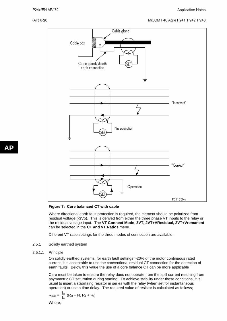
P24x/EN AP/I72
Application Notes (AP) 6-26 MiCOM P40 Agile P241, P242, P243
AP
Figure 7: Core balanced CT with cable
Where directional earth fault protection is required, the element should be polarized from residual voltage (-3Vo). This is derived from either the three phase VT inputs to the relay or the residual voltage input. The VT Connect Mode, 3VT, 2VT+VResidual, 2VT+Vremanent can be selected in the CT and VT Ratios menu.
Different VT ratio settings for the three modes of connection are available.
2.5.1 Solidly earthed system
2.5.1.1 Principle On solidly earthed systems, for earth fault settings >20% of the motor continuous rated current, it is acceptable to use the conventional residual CT connection for the detection of earth faults. Below this value the use of a core balance CT can be more applicable
Care must be taken to ensure the relay does not operate from the spill current resulting from asymmetric CT saturation during starting. To achieve stability under these conditions, it is usual to insert a stabilizing resistor in series with the relay (when set for instantaneous operation) or use a time delay. The required value of resistor is calculated as follows;
Rstab = (Rct + N. R1 + Rr)
Where; o
st
II
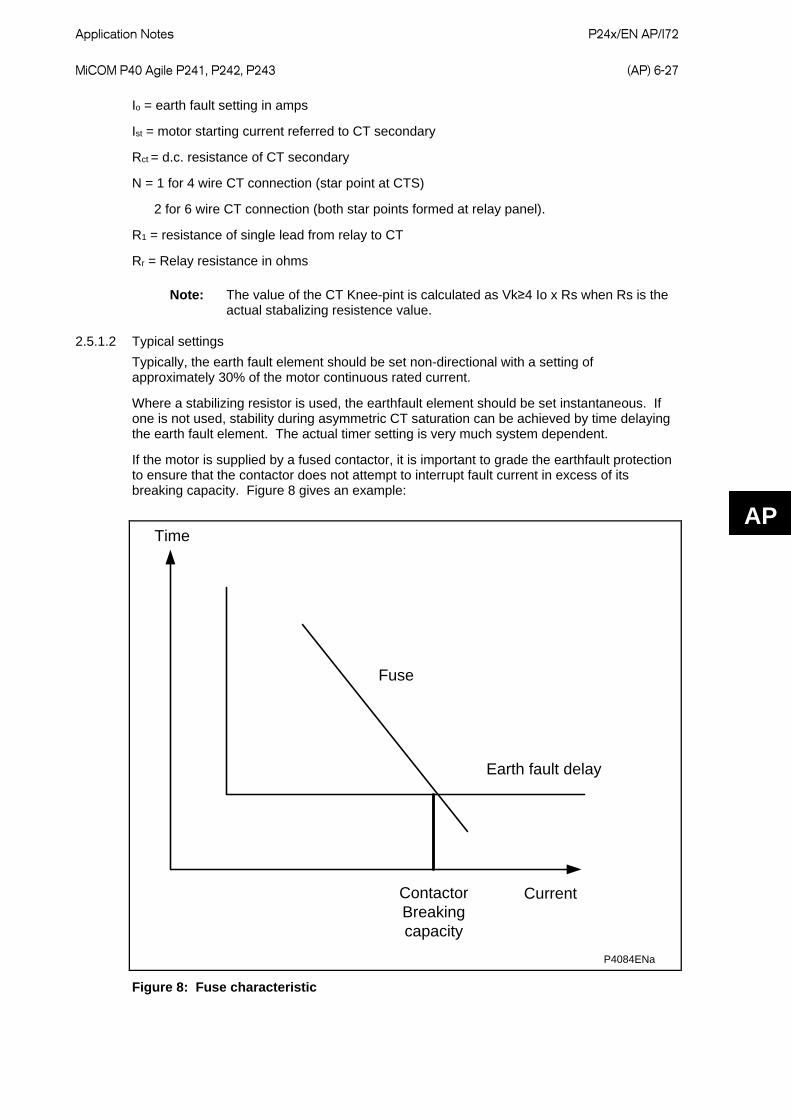
Application Notes
P24x/EN AP/I72 MiCOM P40 Agile P241, P242, P243 (AP) 6-27
AP
Io = earth fault setting in amps
Ist = motor starting current referred to CT secondary
Rct = d.c. resistance of CT secondary
N = 1 for 4 wire CT connection (star point at CTS)
2 for 6 wire CT connection (both star points formed at relay panel).
R1 = resistance of single lead from relay to CT
Rr = Relay resistance in ohms
Note: The value of the CT Knee-pint is calculated as Vk≥4 Io x Rs when Rs is the actual stabalizing resistence value.
2.5.1.2 Typical settings Typically, the earth fault element should be set non-directional with a setting of approximately 30% of the motor continuous rated current.
Where a stabilizing resistor is used, the earthfault element should be set instantaneous. If one is not used, stability during asymmetric CT saturation can be achieved by time delaying the earth fault element. The actual timer setting is very much system dependent.
If the motor is supplied by a fused contactor, it is important to grade the earthfault protection to ensure that the contactor does not attempt to interrupt fault current in excess of its breaking capacity. Figure 8 gives an example:
P4084ENa
Time
Fuse
Earth fault delay
CurrentContactorBreakingcapacity
Figure 8: Fuse characteristic
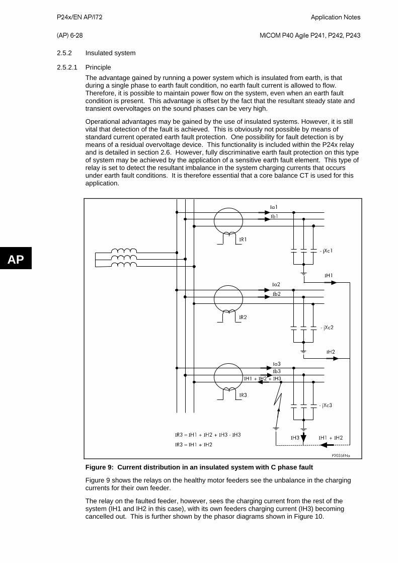
P24x/EN AP/I72
Application Notes (AP) 6-28 MiCOM P40 Agile P241, P242, P243
AP
2.5.2 Insulated system
2.5.2.1 Principle The advantage gained by running a power system which is insulated from earth, is that during a single phase to earth fault condition, no earth fault current is allowed to flow. Therefore, it is possible to maintain power flow on the system, even when an earth fault condition is present. This advantage is offset by the fact that the resultant steady state and transient overvoltages on the sound phases can be very high.
Operational advantages may be gained by the use of insulated systems. However, it is still vital that detection of the fault is achieved. This is obviously not possible by means of standard current operated earth fault protection. One possibility for fault detection is by means of a residual overvoltage device. This functionality is included within the P24x relay and is detailed in section 2.6. However, fully discriminative earth fault protection on this type of system may be achieved by the application of a sensitive earth fault element. This type of relay is set to detect the resultant imbalance in the system charging currents that occurs under earth fault conditions. It is therefore essential that a core balance CT is used for this application.
Figure 9: Current distribution in an insulated system with C phase fault
Figure 9 shows the relays on the healthy motor feeders see the unbalance in the charging currents for their own feeder.
The relay on the faulted feeder, however, sees the charging current from the rest of the system (IH1 and IH2 in this case), with its own feeders charging current (IH3) becoming cancelled out. This is further shown by the phasor diagrams shown in Figure 10.
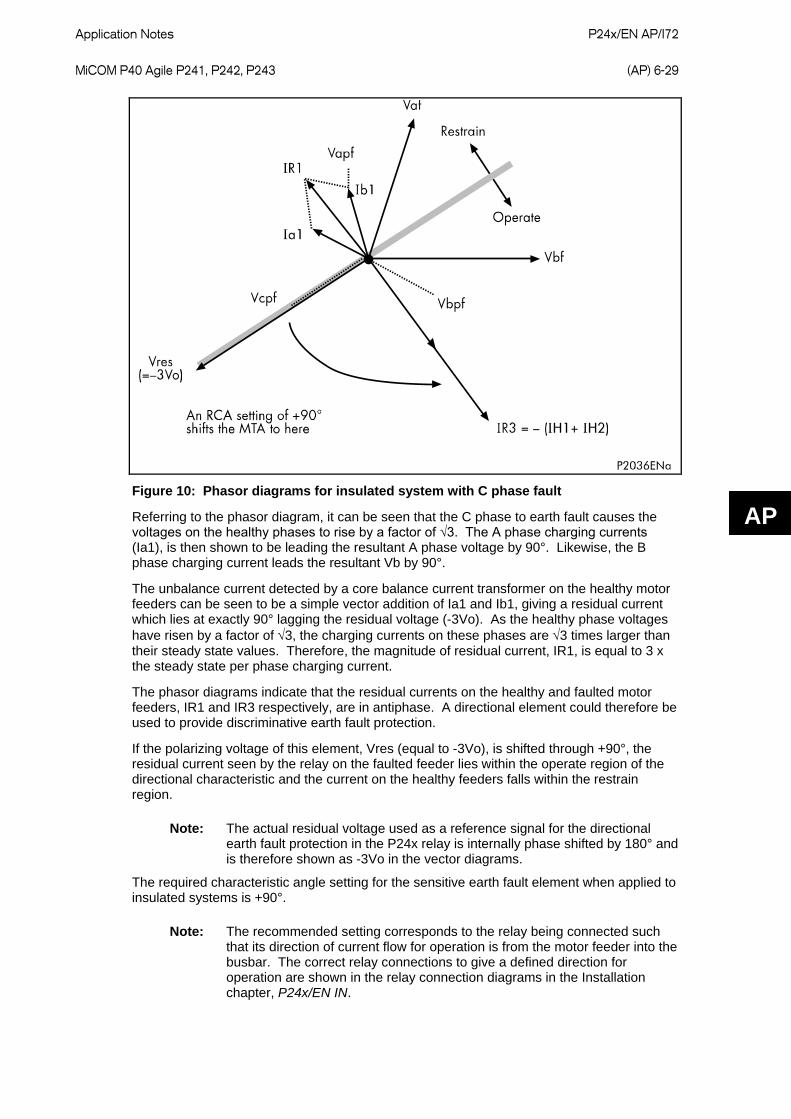
Application Notes
P24x/EN AP/I72 MiCOM P40 Agile P241, P242, P243 (AP) 6-29
AP
Figure 10: Phasor diagrams for insulated system with C phase fault
Referring to the phasor diagram, it can be seen that the C phase to earth fault causes the voltages on the healthy phases to rise by a factor of √3. The A phase charging currents (Ia1), is then shown to be leading the resultant A phase voltage by 90°. Likewise, the B phase charging current leads the resultant Vb by 90°.
The unbalance current detected by a core balance current transformer on the healthy motor feeders can be seen to be a simple vector addition of Ia1 and Ib1, giving a residual current which lies at exactly 90° lagging the residual voltage (-3Vo). As the healthy phase voltages have risen by a factor of √3, the charging currents on these phases are √3 times larger than their steady state values. Therefore, the magnitude of residual current, IR1, is equal to 3 x the steady state per phase charging current.
The phasor diagrams indicate that the residual currents on the healthy and faulted motor feeders, IR1 and IR3 respectively, are in antiphase. A directional element could therefore be used to provide discriminative earth fault protection.
If the polarizing voltage of this element, Vres (equal to -3Vo), is shifted through +90°, the residual current seen by the relay on the faulted feeder lies within the operate region of the directional characteristic and the current on the healthy feeders falls within the restrain region.
Note: The actual residual voltage used as a reference signal for the directional earth fault protection in the P24x relay is internally phase shifted by 180° and is therefore shown as -3Vo in the vector diagrams.
The required characteristic angle setting for the sensitive earth fault element when applied to insulated systems is +90°.
Note: The recommended setting corresponds to the relay being connected such that its direction of current flow for operation is from the motor feeder into the busbar. The correct relay connections to give a defined direction for operation are shown in the relay connection diagrams in the Installation chapter, P24x/EN IN.

P24x/EN AP/I72
Application Notes (AP) 6-30 MiCOM P40 Agile P241, P242, P243
AP
The P24x relay internally derives the residual polarizing voltage for the directional earth fault element. Therefore, either a 5-limb or three single phase VTs should be applied to drive the relay, not a VT of the three-limb design. The former types allow the passage of residual flux through the VT and therefore permit the relay to derive the required residual voltage. A three limb VT provides no path for the flow of residual flux and is therefore unsuitable. Alternatively, the relay can be driven by a phase to phase connected VT with a broken delta winding connected to the residual voltage input.
Note: Discrimination can be provided without the need for directional control. This can only be achieved if it is possible to set the relay in excess of the charging current of the protected feeder and below the charging current for the rest of the system.
2.5.2.2 Setting guidelines The residual current detected by the relay on the faulted feeder is equal to the sum of the charging currents flowing from the rest of the system. The addition of the two healthy phase charging currents on each feeder gives a total charging current which has a magnitude of three times the per phase value. Therefore, the total unbalance current detected by the relay is equal to three times the per phase charging current of the rest of the system. A typical relay setting may therefore be in the order of 30% of this value, that is equal to the per phase charging current of the remaining system. Practically though, the required setting may well be determined on site, where system faults can be applied and suitable settings can be adopted based on practically obtained results. The use of the P24x relays comprehensive measurement and fault recording facilities may prove very useful in this respect.
The timer setting of this element is not critical, since for the first fault only capacitive current exists on the system. However, for subsequent faults, fast tripping is required. If the motor is operated using a fused contactor it is important to delay the protection sufficiently to ensure that the contactor does not attempt to interrupt fault current in excess of its breaking capacity.
2.5.3 Resistance earthed systems Earthing the system using a resistor reduces both the fault current and transient overvoltages. Resistance earthing can sometimes be advantageous in hazardous environments such as in mines since the earthing resistance reduces touch and step potentials during earth faults.
2.5.3.1 Setting guidelines On a resistance earthed system, it is common practice to limit the fault current to approximately full load current.
For such an application, the relay can be set non-directional with a current sensitivity of less than 30% of the minimum earth fault level but greater than three times the steady state charging current of the motor feeder. Figure 9 shows the healthy feeder sees this value of charging current regardless of the method of earthing.
Similar guidelines to those given for solidly earthed systems (section 2.5.1) are applicable with regard to the required time delay setting.
Note: If the above setting guidelines for applying a non-directional relay cannot be achieved due to the current magnitudes, then a sensitive directional earth fault element is required. This eliminates the need to set the relay in excess of the charging current for the protected feeder.
2.5.3.2 High resistance earthing For certain applications, the fault current may be severely limited by the use of very high resistance earthing. It is usual in this case to choose a value of resistor which limits the resistive fault current to a similar magnitude as the system charging current. Therefore, charging current has a marked influence on the angle of the fault current with respect to the polarizing voltage (-3 Vo).
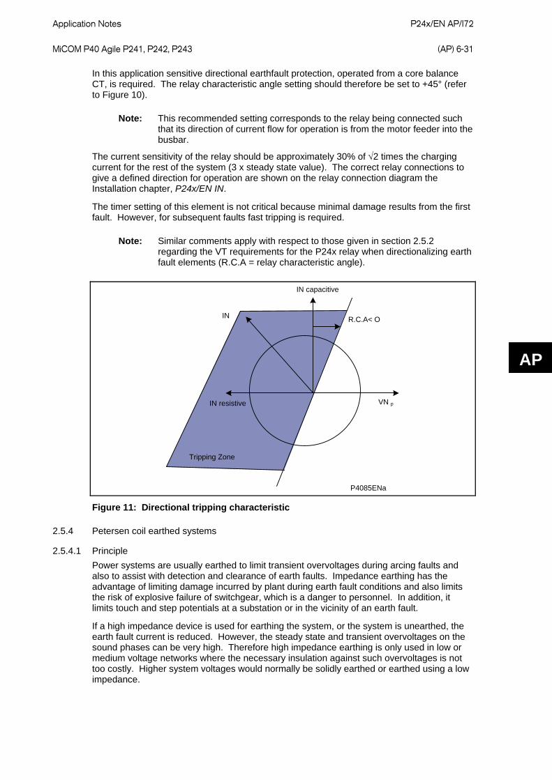
Application Notes
P24x/EN AP/I72 MiCOM P40 Agile P241, P242, P243 (AP) 6-31
AP
In this application sensitive directional earthfault protection, operated from a core balance CT, is required. The relay characteristic angle setting should therefore be set to +45° (refer to Figure 10).
Note: This recommended setting corresponds to the relay being connected such that its direction of current flow for operation is from the motor feeder into the busbar.
The current sensitivity of the relay should be approximately 30% of √2 times the charging current for the rest of the system (3 x steady state value). The correct relay connections to give a defined direction for operation are shown on the relay connection diagram the Installation chapter, P24x/EN IN.
The timer setting of this element is not critical because minimal damage results from the first fault. However, for subsequent faults fast tripping is required.
Note: Similar comments apply with respect to those given in section 2.5.2 regarding the VT requirements for the P24x relay when directionalizing earth fault elements (R.C.A = relay characteristic angle).
P4085ENa
VN p
Tripping Zone
IN resistive
IN
IN capacitive
R.C.A< O
Figure 11: Directional tripping characteristic
2.5.4 Petersen coil earthed systems
2.5.4.1 Principle Power systems are usually earthed to limit transient overvoltages during arcing faults and also to assist with detection and clearance of earth faults. Impedance earthing has the advantage of limiting damage incurred by plant during earth fault conditions and also limits the risk of explosive failure of switchgear, which is a danger to personnel. In addition, it limits touch and step potentials at a substation or in the vicinity of an earth fault.
If a high impedance device is used for earthing the system, or the system is unearthed, the earth fault current is reduced. However, the steady state and transient overvoltages on the sound phases can be very high. Therefore high impedance earthing is only used in low or medium voltage networks where the necessary insulation against such overvoltages is not too costly. Higher system voltages would normally be solidly earthed or earthed using a low impedance.
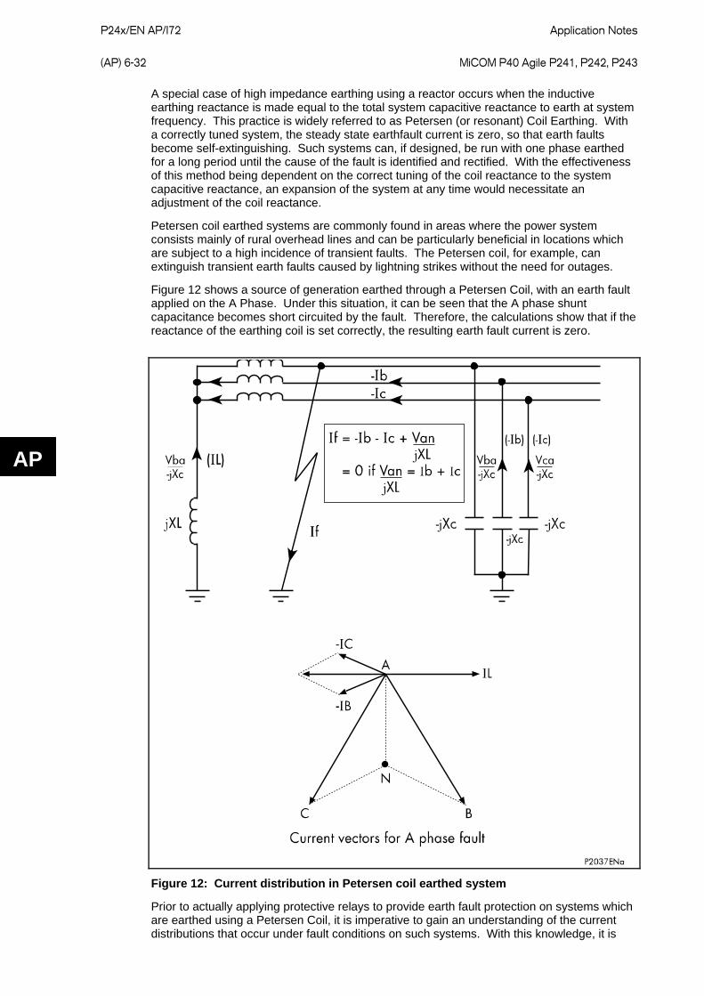
P24x/EN AP/I72
Application Notes (AP) 6-32 MiCOM P40 Agile P241, P242, P243
AP
A special case of high impedance earthing using a reactor occurs when the inductive earthing reactance is made equal to the total system capacitive reactance to earth at system frequency. This practice is widely referred to as Petersen (or resonant) Coil Earthing. With a correctly tuned system, the steady state earthfault current is zero, so that earth faults become self-extinguishing. Such systems can, if designed, be run with one phase earthed for a long period until the cause of the fault is identified and rectified. With the effectiveness of this method being dependent on the correct tuning of the coil reactance to the system capacitive reactance, an expansion of the system at any time would necessitate an adjustment of the coil reactance.
Petersen coil earthed systems are commonly found in areas where the power system consists mainly of rural overhead lines and can be particularly beneficial in locations which are subject to a high incidence of transient faults. The Petersen coil, for example, can extinguish transient earth faults caused by lightning strikes without the need for outages.
Figure 12 shows a source of generation earthed through a Petersen Coil, with an earth fault applied on the A Phase. Under this situation, it can be seen that the A phase shunt capacitance becomes short circuited by the fault. Therefore, the calculations show that if the reactance of the earthing coil is set correctly, the resulting earth fault current is zero.
Figure 12: Current distribution in Petersen coil earthed system
Prior to actually applying protective relays to provide earth fault protection on systems which are earthed using a Petersen Coil, it is imperative to gain an understanding of the current distributions that occur under fault conditions on such systems. With this knowledge, it is
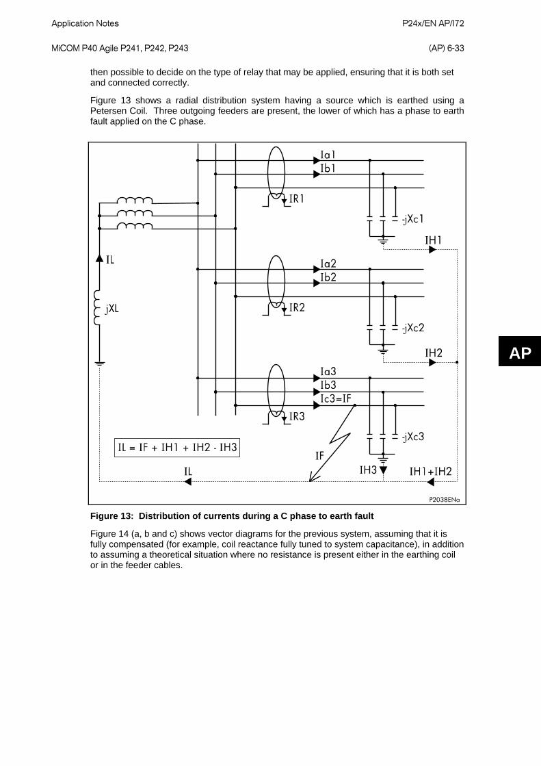
Application Notes
P24x/EN AP/I72 MiCOM P40 Agile P241, P242, P243 (AP) 6-33
AP
then possible to decide on the type of relay that may be applied, ensuring that it is both set and connected correctly.
Figure 13 shows a radial distribution system having a source which is earthed using a Petersen Coil. Three outgoing feeders are present, the lower of which has a phase to earth fault applied on the C phase.
Figure 13: Distribution of currents during a C phase to earth fault
Figure 14 (a, b and c) shows vector diagrams for the previous system, assuming that it is fully compensated (for example, coil reactance fully tuned to system capacitance), in addition to assuming a theoretical situation where no resistance is present either in the earthing coil or in the feeder cables.
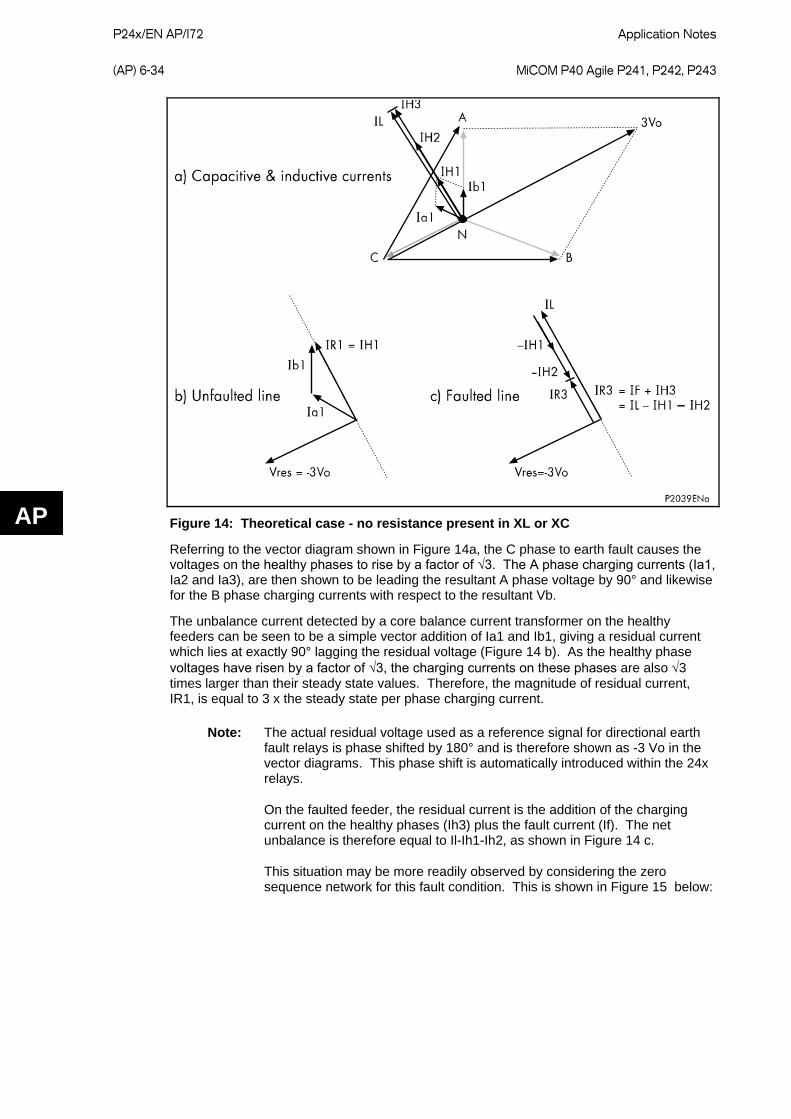
P24x/EN AP/I72
Application Notes (AP) 6-34 MiCOM P40 Agile P241, P242, P243
AP
Figure 14: Theoretical case - no resistance present in XL or XC
Referring to the vector diagram shown in Figure 14a, the C phase to earth fault causes the voltages on the healthy phases to rise by a factor of √3. The A phase charging currents (Ia1, Ia2 and Ia3), are then shown to be leading the resultant A phase voltage by 90° and likewise for the B phase charging currents with respect to the resultant Vb.
The unbalance current detected by a core balance current transformer on the healthy feeders can be seen to be a simple vector addition of Ia1 and Ib1, giving a residual current which lies at exactly 90° lagging the residual voltage (Figure 14 b). As the healthy phase voltages have risen by a factor of √3, the charging currents on these phases are also √3 times larger than their steady state values. Therefore, the magnitude of residual current, IR1, is equal to 3 x the steady state per phase charging current.
Note: The actual residual voltage used as a reference signal for directional earth fault relays is phase shifted by 180° and is therefore shown as -3 Vo in the vector diagrams. This phase shift is automatically introduced within the 24x relays.
On the faulted feeder, the residual current is the addition of the charging current on the healthy phases (Ih3) plus the fault current (If). The net unbalance is therefore equal to Il-Ih1-Ih2, as shown in Figure 14 c.
This situation may be more readily observed by considering the zero sequence network for this fault condition. This is shown in Figure 15 below:
Application Notes
P24x/EN AP/I72 MiCOM P40 Agile P241, P242, P243 (AP) 6-35
AP
Figure 15: Zero sequence network showing residual currents
In comparing the residual currents occurring on the healthy and on the faulted feeders (Figure 16 b & 16c), it can be seen that the currents would be similar in both magnitude and phase; so it would not be possible to apply a relay which could provide discrimination.
However, the scenario of no resistance being present in the coil or feeder cables is purely theoretical. Further consideration therefore needs to be given to a practical application in which the resistive component is no longer ignored, see Figure 16.
P24x/EN AP/I72
Application Notes (AP) 6-36 MiCOM P40 Agile P241, P242, P243
AP
Figure 16: Practical case:- resistance present in XL and Xc
Figure 16a again shows the relationship between the capacitive currents, coil current and residual voltage. It can now be seen that due to the presence of resistance in the feeders, the healthy phase charging currents are now leading their respective phase voltages by less than 90°. In a similar manner, the resistance present in the earthing coil has the effect of shifting the current, IL, to an angle less than 90° lagging. The result of these slight shifts in angles can be seen in Figure 16b and 16c.
The residual current now appears at an angle in excess of 90° from the polarizing voltage for the unfaulted feeder and less than 90° on the faulted feeder. Therefore, a directional relay with a characteristic angle setting of 0° (with respect to the polarizing signal of -3Vo) could be applied to provide discrimination. The healthy feeder residual current would appear in the restrain section of the characteristic but the residual current on the faulted feeder would be in the operate region.
In practical systems a resistance is inserted in parallel with the earthing coil. This increases the level of earth fault current to a more detectable level. It also increases the angular difference between the residual signals to help the application of discriminating protection.
2.5.4.2 Operation of sensitive earth fault element The angular difference between the residual currents on the healthy and faulted feeders allows a directional relay to be applied whose zero torque line passes between the two currents. The following types of protection elements may be applied for earth fault detection.
• A suitably sensitive directional earth fault relay having a relay characteristic angle setting (RCA) of zero degrees, with the possibility of fine adjustment about this threshold.
• A sensitive directional zero sequence wattmetric relay having similar requirements to the above with respect to the required RCA settings.
Both stages 1 and 2 of the sensitive earth fault element of the P24x relay are settable down to 0.2% of rated current and would therefore fulfill the requirements of the first method listed above and could therefore be applied successfully. However, many utilities (particularly in
Application Notes
P24x/EN AP/I72 MiCOM P40 Agile P241, P242, P243 (AP) 6-37
AP
central Europe) have standardized on the wattmetric method of earth fault detection, which is described in the following section.
Zero sequence power measurement, as a derivative of Vo and Io, offers improved relay security against false operation with any spurious core balance CT output for non earth fault conditions. This is also the case for a sensitive directional earth fault relay having an adjustable Vo polarizing threshold.
2.5.5 Wattmetric characteristic
2.5.5.1 Principle The previous analysis shows that a small angular difference exists between the spill current on the healthy and faulted feeders. This angular difference gives rise to active components of current which are in antiphase to one another. This is shown in Figure 17 below:
Figure 17: Resistive components of spill current
Therefore, the active components of zero sequence power lies in similar planes. On a relay capable of detecting active power it would be able to make a discriminatory decision. That is, if the wattmetric component of zero sequence power was detected in the forward direction, then this would be indicative of a fault on that feeder; if power was detected in the reverse direction, then the fault must be present on an adjacent feeder or at the source.
For operation of the directional earth fault element within the P24x relays, all three of the settable thresholds on the relay must be exceeded; namely the current (P0>Current Set), the voltage (P0>Voltage Set) and the power (P0>Coef. K Set). The directional decision within the relays is based on current rather than power. The 'Coef. K' threshold is simply present as an additional level that must be exceeded before a trip is initiated.
The wattmetric power formula is calculated using residual rather than zero sequence quantities. Residual quantities are three times their respective zero sequence values and so the complete formula for operation is shown below:-
The wattmetric element setting corresponds to:
Vres x Ires x Cos (Φ-Φc)= 9 x Vo x Io x Cos (Φ - Φc)
Where;
Φ = Angle between the Polarizing Voltage (-Vres) and the Residual Current
Φc = Relay Characteristic Angle (RCA) Setting (ISEF> Char Angle)
Vres = Residual Voltage
Ires = Residual Current
Vo = Zero Sequence Voltage
Io = Zero Sequence Current
P24x/EN AP/I72
Application Notes (AP) 6-38 MiCOM P40 Agile P241, P242, P243
AP
2.5.5.2 Application considerations Required relay current and voltage connections:
Referring to the relevant application diagram for the P24x relay, it should be applied such that its direction for forward operation is looking down into the protected feeder (away from the busbar), with a 0° RCA setting.
The relay application diagram shows it is usual for the earth fault element to be driven from a core balance current transformer (CBCT). This eliminates the possibility of spill current that may arise from slight mismatches between residually connected line CT's. It also enables a much lower CT ratio to be applied, thereby allowing the required protection sensitivity to be more easily achieved.
2.5.5.3 Calculation of required relay settings: As has been previously shown, for a fully compensated system, the residual current detected by the relay on the faulted feeder is equal to the coil current minus the sum of the charging currents flowing from the rest of the system. Further, as stated in the previous section, the addition of the two healthy phase charging currents on each feeder gives a total charging current which has a magnitude of three times the steady state per phase value. Therefore, for a fully compensated system, the total unbalance current detected by the relay is equal to three times the per phase charging current of the faulted circuit. A typical relay setting may therefore be in the order of 30% of this value, i.e. equal to the per phase charging current of the faulted circuit. Practically though, the required setting may well be determined on site, where system faults can be applied and suitable settings can be adopted based on practically obtained results.
Also, in most situations, the system is not fully compensated and therefore a small level of steady state fault current is allowed to flow. The residual current seen by the relay on the faulted feeder may therefore be a larger value, which further emphasizes the fact that relay settings should be based on practical current levels, wherever possible.
The above also holds true regarding the required Relay Characteristic Angle (RCA) setting. As has been shown earlier, a nominal RCA setting of 0º is required. However, fine tuning of this setting is required on site to obtain the optimum setting in accordance with the levels of coil and feeder resistances present. The loading and performance of the CT has an effect in this regard. The effect of CT magnetizing current creates phase lead of current. While this assists with operation of faulted feeder relays it reduces the stability margin of healthy feeder relays. A compromise can therefore be reached through fine adjustment of the RCA. This is adjustable in 1° steps on the P24x relays.
2.6 Residual overvoltage (neutral displacement) protection (59N) On a healthy three phase power system, the addition of each of the three phase to earth voltages is nominally zero, as it is simply the vector addition of three balanced vectors at 120° to one another. However, when an earth fault occurs on the primary system, this balance is upset and a 'residual' voltage is produced. This could be measured, for example, at the secondary terminals of a voltage transformer having a "broken delta" secondary connection.
Note: This condition causes a rise in the neutral voltage with respect to earth which is commonly referred to as "neutral voltage displacement" or NVD.
Therefore, it can be seen that the detection of a residual overvoltage condition is an alternative means of earth fault detection which does not require any measurement of current. This may be particularly advantageous in high impedance earthed / insulated systems, where the provision of core balance CT's on each feeder may be either impractical or uneconomic.
Note: Where residual overvoltage protection is applied, such a voltage is generated for a fault occurring anywhere on that section of the system and so the applied protection must be discriminative. The NVD element within the P24x relay is of two stage design, each stage having separate voltage and time delay settings. Stage 1 may be set to operate on either an IDMT or DT characteristic, whilst stage 2 may be set to DT only.

Application Notes
P24x/EN AP/I72 MiCOM P40 Agile P241, P242, P243 (AP) 6-39
AP
The IDMT characteristic available on the first stage is defined by the following formula:
t = TMS / (1 - M)
Where;
TMS = Time Multiplier Setting
t = Operating Time in Seconds
M = Derived Residual Voltage / Relay Setting Voltage
Two stages are included for this NVD protection to account for applications which require both alarm and trip stages. In such applications, an alarm is usually required to be generated soon after the condition is detected which simply serves to indicate the presence of an earth fault on the system. The system has been designed to withstand the associated healthy phase overvoltages for several hours following fault inception. This therefore gives time for system operators to find and remove the fault condition.
This element should be driven from residual voltage (-3Vo). This can be derived from either the three phase VT inputs to the relay or the residual voltage input. The VT Connect Mode, 3VT, 2VT+VResidual, 2VT+Vremanent can be selected in the CT and VT Ratios menu.
Different VT ratio settings for the three modes of connection are available.
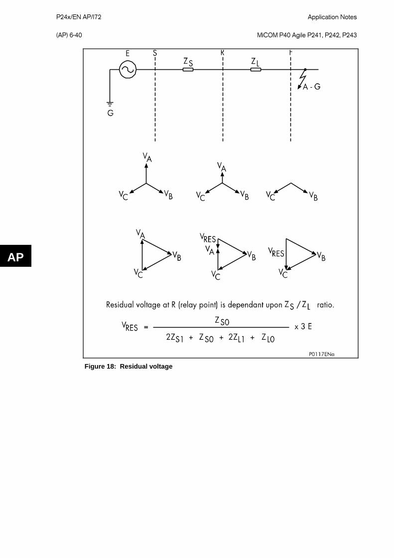
P24x/EN AP/I72
Application Notes (AP) 6-40 MiCOM P40 Agile P241, P242, P243
AP
Figure 18: Residual voltage
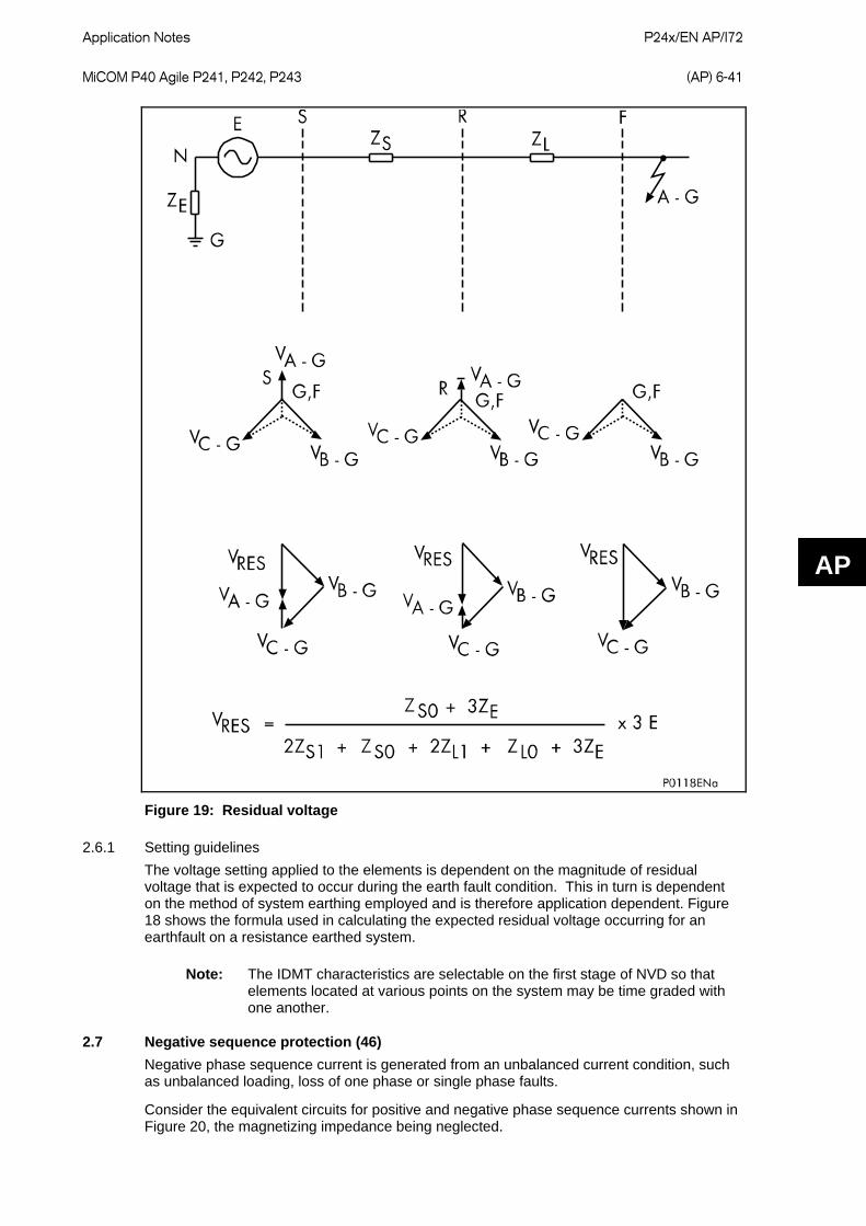
Application Notes
P24x/EN AP/I72 MiCOM P40 Agile P241, P242, P243 (AP) 6-41
AP
Figure 19: Residual voltage
2.6.1 Setting guidelines The voltage setting applied to the elements is dependent on the magnitude of residual voltage that is expected to occur during the earth fault condition. This in turn is dependent on the method of system earthing employed and is therefore application dependent. Figure 18 shows the formula used in calculating the expected residual voltage occurring for an earthfault on a resistance earthed system.
Note: The IDMT characteristics are selectable on the first stage of NVD so that elements located at various points on the system may be time graded with one another.
2.7 Negative sequence protection (46) Negative phase sequence current is generated from an unbalanced current condition, such as unbalanced loading, loss of one phase or single phase faults.
Consider the equivalent circuits for positive and negative phase sequence currents shown in Figure 20, the magnetizing impedance being neglected.
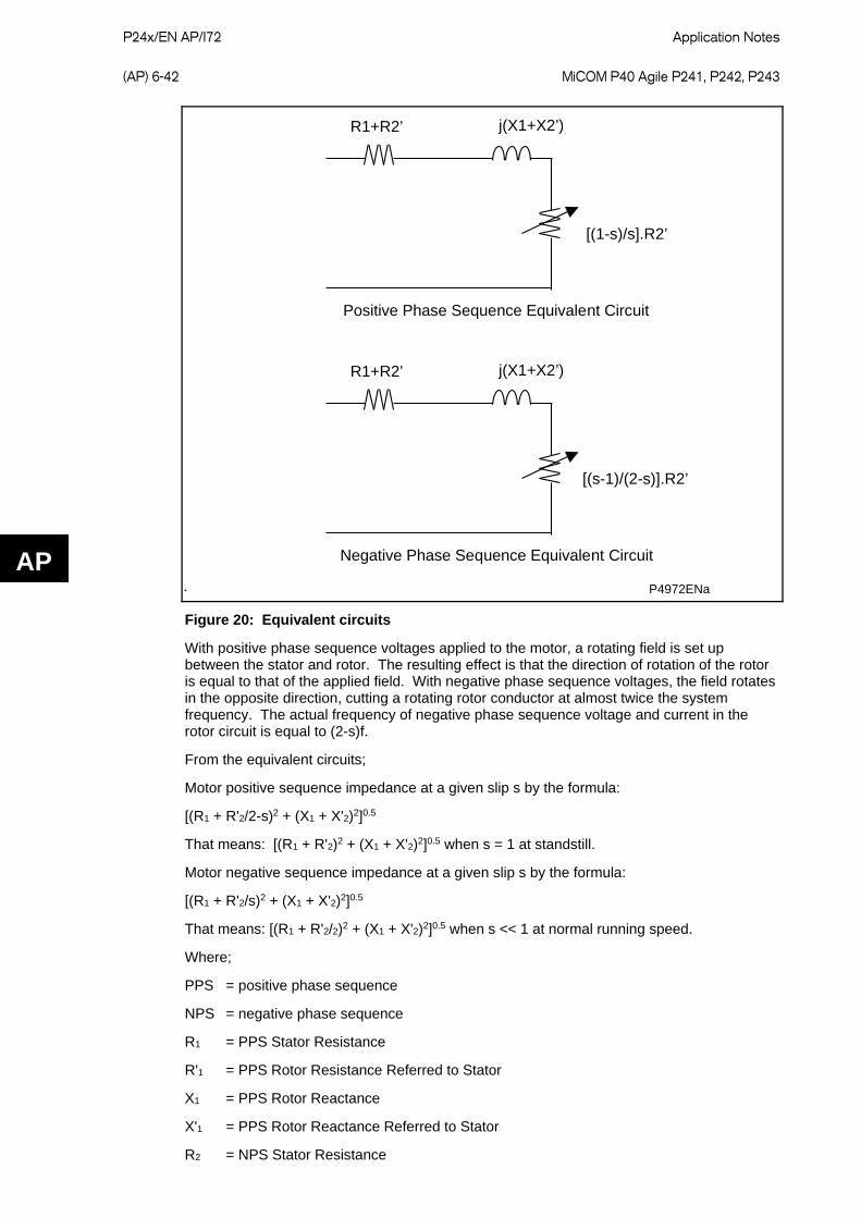
P24x/EN AP/I72
Application Notes (AP) 6-42 MiCOM P40 Agile P241, P242, P243
AP
R1+R2’ j(X1+X2’)
[(1-s)/s].R2’
Positive Phase Sequence Equivalent Circuit
R1+R2’ j(X1+X2’)
[(s-1)/(2-s)].R2’
Negative Phase Sequence Equivalent Circuit
P4972ENa
Figure 20: Equivalent circuits
With positive phase sequence voltages applied to the motor, a rotating field is set up between the stator and rotor. The resulting effect is that the direction of rotation of the rotor is equal to that of the applied field. With negative phase sequence voltages, the field rotates in the opposite direction, cutting a rotating rotor conductor at almost twice the system frequency. The actual frequency of negative phase sequence voltage and current in the rotor circuit is equal to (2-s)f.
From the equivalent circuits;
Motor positive sequence impedance at a given slip s by the formula:
[(R1 + R'2/2-s)2 + (X1 + X'2)2]0.5
That means: [(R1 + R'2)2 + (X1 + X'2)2]0.5 when s = 1 at standstill.
Motor negative sequence impedance at a given slip s by the formula:
[(R1 + R'2/s)2 + (X1 + X'2)2]0.5
That means: [(R1 + R'2/2)2 + (X1 + X'2)2]0.5 when s << 1 at normal running speed.
Where;
PPS = positive phase sequence
NPS = negative phase sequence
R1 = PPS Stator Resistance
R'1 = PPS Rotor Resistance Referred to Stator
X1 = PPS Rotor Reactance
X'1 = PPS Rotor Reactance Referred to Stator
R2 = NPS Stator Resistance
Application Notes
P24x/EN AP/I72 MiCOM P40 Agile P241, P242, P243 (AP) 6-43
AP
R'2 = NPS Rotor Resistance Referred to Stator
X2 = NPS Rotor Reactance
X'2 = NPS Rotor Reactance Referred to Stator
s = Slip
The value of resistance is generally much less than the leakage reactance. Therefore, neglecting the resistance term, the motor negative phase sequence impedance at normal running speed can be approximated to the positive phase sequence impedance at standstill.
At normal running speed;
current load normalcurrent starting
impedance sequence negativeimpedance sequence positive ≅
For example, if a motor has a starting current of six times the full load value, the negative sequence impedance would be about 1/6 the positive sequence impedance.
Therefore, the presence of 5% negative sequence voltage in the supply would result in approximately 30% of negative sequence current.
The a.c. resistance of the rotor conductor to the induced negative sequence current is greater due to the higher frequency [(2-s)f], causing skin effect. The heating effect of negative sequence current is therefore greater and increases the motor losses.
It is therefore essential to detect any negative sequence current present on the system and act accordingly before dangerous temperatures occur in the motor.
The P24x relay includes several methods for the detection of negative phase sequence currents, depending on the cause of the unbalance. These methods are addressed in detail below.
2.7.1 Loss of one phase while starting & running
2.7.1.1 Principle If a motor is started with one phase open, it remains stationary and it can draw a current equal to 0.866 times the normal starting current. Under these circumstances, the negative phase sequence component present in the current is equal to half the normal starting current value. This is an extreme condition, as this amount of negative phase sequence current rapidly overheats the motor, and unless corrective action is taken, the motor will be seriously damaged.
Loss of one phase of the supply to a motor during normal running conditions, results in the following conditions:
Heating increases considerably due to high rotor losses caused by the -ve sequence current now present
Output of the motor is reduced and, depending on the load, an induction motor may stall or a synchronous motor may pull out of synchronism,
The motor current will increase.
One common factor in the aforementioned conditions is the presence of negative phase sequence current. The P24x relay therefore incorporates a negative phase sequence current element to detect such extreme operating conditions. This negative phase sequence current element operating time characteristic is of an inverse time nature and is governed by the following formula;
t = TMS * [1.2/(I2/Is)] for I2/Is ≤ 2
t = TMS * 0.6 for I2/Is >2
The element may be selectively enabled or disabled.
In addition to this, an independent, definite time alarm stage is provided.

P24x/EN AP/I72
Application Notes (AP) 6-44 MiCOM P40 Agile P241, P242, P243
AP
2.7.1.2 Setting guidelines This element should be set in excess of the anticipated negative phase sequence current resulting from asymmetric CT saturation during starting, but less than the negative phase sequence current resulting from loss of one phase during starting.
A typical setting for the negative sequence overcurrent element is 30% of the anticipated negative sequence current resulting from loss of one phase during starting for a motor with a starting current to load current ratio of 6 to 1.
Therefore set:
I2>2 Current Set = 1/6 normal starting current or full load current The setting for the alarm time delay is application dependent.
2.7.2 3 Phase voltage check (reverse phase detection) (47/27)
2.7.2.1 Principle Incorrect phase rotation of the incoming supply to the motor results in the motor rotating in the opposite direction. For certain directionally sensitive applications, such as lifts and conveyor belts, this is a potentially dangerous condition and must be detected rapidly.
Although the above condition does not result in the flow of negative phase sequence current in the motor, 100% negative phase sequence current are presented to the measuring circuitry of the relay.
If the machine is allowed to rotate in the opposite direction, the thermal protection and negative phase sequence overcurrent element detects the condition and trips the circuit breaker in their respective time delays. However, it is sometimes better not to allow the motor to rotate at all.
For such applications, the P24x relay includes a 3 phase voltage check detector. This element monitors the input voltage rotation and magnitude. The positive sequence voltage should be greater than the negative sequence voltage and the phase voltages VA, VB and VC should be greater than the user settable threshold. If the aforementioned conditions are not satisfied then an alarm is raised. This alarm contact can be interlocked with the motor contactor or circuit breaker to prevent the motor from being energized until correct phase rotation and sufficient voltage exist on the system.
This feature requires a 52a circuit breaker auxiliary contact mapped to an opto input to get the information CBclosed/CB open.
2.7.2.2 Setting guidelines The undervoltage interlock (Start Low V Set) is provided to prevent the motor attempting to start on reduced voltage. The setting is system dependent but may typically be set to 80% - 90% of Vn.
2.8 Start / stall protection (48/51LR/50S/14) When a motor is started, it draws a value of current in excess of full load rating for a set period of time, namely the starting time. It is normal practice to assume a constant starting current for the whole of the starting time.
The starting current varies depending on the type and method of starting utilized. If the motor is started direct-on-line (DOL), the current could easily reach 6 times full load current. However, when star/delta starting is utilized, the starting current is √3 less than when DOL starting.
If a motor stalls while running, or is unable to start due to excessive loading, it draws a current equivalent to the locked rotor current. The level of starting current is equal to the level of locked rotor current, therefore it is not possible to distinguish between 3 phase stalling and healthy starting by monitoring current alone.
In the majority of cases the starting time of a normal induction motor is less than the maximum stall withstand time. Under this condition it is possible to discriminate on a time basis between the two conditions and therefore provide protection against stalling.
Application Notes
P24x/EN AP/I72 MiCOM P40 Agile P241, P242, P243 (AP) 6-45
AP
However, where motors are used to drive high inertia loads, the stall withstand time may be less than the starting time. In such cases, it is not possible to discriminate between start and stall conditions by time alone.
The P24x relay provides extensive start and stall protection, in order that all of the aforementioned conditions may be accounted for. The methods used to achieve this are discussed in more detail below.
This feature requires a 52a circuit breaker auxiliary contact mapped to an opto input to get the information CBclosed/CB open.
2.8.1 Excessive start time/locked rotor protection - stall time > start time (51LR) A motor may fail to accelerate for several reasons. For example, loss of one supply phase, mechanical failure or insufficient supply voltage. Failure of a machine to accelerate results in excessive current being drawn by the motor. This current generates extremely high temperatures within the machine. The motor does not have the added cooling normally provided by rotation, therefore irreparable damage will result very quickly.
Where the stall withstand time is less than the starting time, it is possible to utilize a contact from a speed sensing device wired into a specified opto input (Speed Input: DDB 104) in conjunction with measurement of the phase current to detect a safe start.
Three methods are available for detecting a start and they are menu selectable. See the Operation chapter, P24x/EN OP, for detailed information.
2.8.1.1 Setting guidelines The starting current threshold should be set greater than full load current, but less than motor starting current. Where the stall withstand time is greater than the starting time, timer – Prol Start Time - should be set 1 or 2 seconds above the motor starting time and less than the cold stall withstand time. The Prolonged Start needs to be set to Enabled for this function to operate.
Setting example:
Utilizing the previously specified motor parameters;
Starting current = 3 x Ith = 882A
Prolonged start time = 12 seconds. These settings are shown in Figure 1.
2.8.2 Stall protection (50S)
2.8.2.1 Principle An induction motor may stall for several reasons, such as overloading or undervoltage. When a machine stalls it runs down while drawing a current equal to the locked rotor current.
Where the stall withstand time is greater than the starting time, a stall condition during running is simply detected by the line current exceeding the programmed threshold. If the current fails to fall back below this threshold before the programmed time delay has elapsed, a trip can be initiated.
Note: This function is disabled when the relay detects a start condition.
2.8.2.2 Setting guidelines The stall current threshold (Stall Setting) should be set greater than full load current, but less than motor stall current (which is usually equal to starting current). Its corresponding timer (Stall Time) should be set less than the motor hot stall withstand time. The Stall Detection needs to be set to Enabled for this function to operate.
Setting example:
Utilizing the previously specified motor parameters;
Stall Setting = 3 x Ith = 882 A

P24x/EN AP/I72
Application Notes (AP) 6-46 MiCOM P40 Agile P241, P242, P243
AP
Stall Time = 6 seconds
These settings are shown in Figure 1.
2.8.3 Excessive start time/locked rotor protection - stall time < start time (14) As the rotor resistance of an induction motor is proportional to slip, it decreases during acceleration. When the motor is stationary, the rotating field in the air gap, set up by currents flowing in the stator winding will cut the rotor. This field travels at synchronous speed relative to the rotor and induces a voltage at system frequency, therefore generating circulating currents in the rotor bars. At this frequency, the reactance of the rotor causes the current to flow in the outer section of the rotor conductors; commonly known as the 'skin effect'. Since the current is occupying a smaller section of the rotor, the apparent impedance presented to it is increased, therefore the I2R heating is greatly increased. As the motor accelerates during starting the slip begins to decrease and the current is able to occupy more of the rotor conductor. The apparent impedance therefore reduces along with the heating effect. The motor is therefore able to tolerate starting current for the starting time, but not locked rotor current.
The above description explains why, for certain applications, such as motors driving high inertia loads, the stall withstand time may be safely exceeded during starting, without resulting in an overtemperature condition within the motor. Therefore , since the stall withstand time is less than the start time, it is not possible to use time alone to distinguish between a start and a stall condition.
Where the stall withstand time is less than the starting time, it is possible to utilize a contact from a speed sensing device wired into a specified opto input (Speed Input: DDB 104) in conjunction with measurement of the phase current to detect a safe start.
2.8.3.1 Setting guidelines The Starting current threshold (Starting current) should be set greater than full load current, but less than motor locked rotor current (usually equal to starting current). Its corresponding timer (Stall Time) should be set less than the motor cold stall withstand time. The Stall Rotor-str needs to be set to Enabled for this function to operate.
2.8.4 Number of starts limitation (66) Repeated starting, or intermittent operation of a motor, may generate dangerously high temperatures within the motor, unless sufficient time is allowed for cooling between starts.
The P24x relay incorporates several starts limitation facilities. This limitation is fully programmable and is applicable to both hot and cold start conditions. A hot start is defined by a thermal state greater than 50% and a cold start is defined as a thermal state lower than 50%.
Restarting the motor from a hot thermal state:
For certain applications, it is not desirable to allow the motor time to cool down to a specified thermal state before a re-start is permitted. The P24x relay incorporates several features which allow a subsequent start from a hot thermal state, these are discussed in the section on 'thermal overload protection'.
The motor accumulated run time displayed in the menu cell “Motor Run Time” of the “Measurement 3” menu is initiated each time the switching device is closed and remains closed.

Application Notes
P24x/EN AP/I72 MiCOM P40 Agile P241, P242, P243 (AP) 6-47
AP
2.8.5 Anti-Backspin protection (27 Abs) A motor may be driving a very high inertia load. Once the CB/Contactor supplying power to the motor is switched off, the rotor may continue to turn for a considerable length of time as it decelerates. The motor now becomes a generator and applying supply voltage out of phase can result in catastrophic failure. In some other applications for example when a motor is on a down-hole pump, after the motor stops, the liquid may fall back down the pipe and spin the rotor backwards. Don’t start the motor at this time. In these circumstances the anti-backspin function is used to detect when the rotor has stopped, to allow re-starting of the motor.
The operation of this function depends on the parameter VT connecting mode: If this is set to 2 VT + Vremanent, then the function uses an undervoltage with the connected Phase-Phase remanent voltage. If not, the function uses only a time delay.
2.8.6 Setting guidelines for ABS protection The voltage threshold setting for the anti-backspin protection VRem Antibacks should be set at some low value to indicate that the motor is stopped. The default setting of 10 V secondary is adequate for most applications.
If the VT connecting mode is set to 2 VT + Vremanent the time delay Antibacks Delay must be set to an adequate time for the motor to stop after and the remanent voltage has dropped below the VRem Antibacks setting following a trip.
If the VT connecting mode is not set to 2 VT + Vremanent then the time delay Antibacks Delay must be set to an adequate time for the motor to stop after the trip. The default setting of 3000 s is adequate for the majority of applications.
2.8.7 Momentary reduction in system voltage during running of the motor In cases when the supply voltage falls below a settable under voltage threshold, the duration of the fall in voltage can be classified as short, medium, or long (corresponding to “Reac Time”, “Reac Long Time” and “Reac Shed Time” respectively of P24x relay designations).
• Short falls are intended to cover situations when it is appropriate to authorize reacceleration of the rotor and not to issue a trip order after voltage restoration is detected via a settable under voltage threshold.
• Medium falls are intended to cover situations for when the voltage has not been recovered within a set short time detected via a settable over voltage threshold and the motor has tripped as a result, but it is appropriate to automatically restart the motor within a set long time after the voltage has become restored. Detection of restored voltage is based on a settable over voltage threshold.
• Long falls are intended to cover cases when restoration is from back-up power, and there must be substantial intervals between starting different motors to maintain stability, and/or only critical motors can be started.
A short fall in voltage from the electrical network causes a reduction in rotor speed. If the motor was running at the time a short fall occurred, a forced reacceleration occurs as soon as the relay detects healthy supply voltage. A forced reacceleration bypasses any pre-staged start-up sequence the starter type might otherwise provide.
When the voltage is restored, the rotor starts on a reacceleration phase to regain its nominal speed. This reacceleration manifests itself as an intake of current of approximately the same value as that of the locked rotor current, its duration being relative to the magnitude of the fall in voltage and the duration of the fall in voltage.
2.8.7.1 Low voltage protection (reacceleration authorization) Following a transient dip in the supply voltage, a motor will attempt to re-accelerate. Under these circumstances it will draw a level of current exceeding the relay stall protection threshold, (Stall Setting). Therefore , for successful re-acceleration the P24x relay can be configured to temporarily inhibit the stall protection.
If a low voltage condition exists on the system for a time in excess of 100 ms, on recovery of the voltage the relay will inhibit stall protection. Reacceleration is recognized if current above the set threshold is detected within 5 seconds of the voltage recovery. During this

P24x/EN AP/I72
Application Notes (AP) 6-48 MiCOM P40 Agile P241, P242, P243
AP
period the excessive start protection is enabled. This provides protection in the event of unsuccessful reacceleration. For example, a dip in the busbar voltage supplying several motors would result in each of them attempting reacceleration. Subsequently, a large current is drawn from the supply, therefore further reducing the supply voltage, resulting in potential stalling of all machines. This would not occur during normal starting as a staggered approach is normally adopted.
This function is disabled during the starting period, and requires a 52a circuit breaker auxiliary contact mapped to an opto input to get the information CBclosed/CB open.
Setting Guidelines:
The low voltage threshold (Reac Low V Set) is very much system dependent, however a typical setting may be 0.8-0.9 Vn.
2.8.7.2 AUTO RE-START authorization: Re-start/load restoration
When enabled, the Auto-Restart feature is available to carry out automatic re-starting of the motor on restoration of supply for cases when duration of the voltage fall is medium or long.
The AUTO RE-START element provides for controlling the timing of controlled starts following interruptions.
The automatic re-start of the motor is carried out after a medium set time delay Treac-long or after an extended long time delay Treac-shed. Treac-long threshold setting can be used for when it is appropriate to restart the motor with any staged startup sequence the starter type might provide. Treac-shed threshold setting can be used for to cover cases when restoration is from backup power, and there must be substantial delays between starting different motors to maintain stability, and/or only critical motors can be started. The Auto re-start feature, if enabled, becomes active after the relay has issued a trip signal due to a voltage sag condition with duration longer than Treacc threshold.
If Treac-long is set to a value other than Zero (off) and after a trip order has been issued (due to the supply voltage not being restored within the time interval of Treac), the P24x relay initiates Treac-long time-delay.
If the supply is restored within Treac-long time delay interval, a close order is issued by the relay and a normal start is allowed to initiate. If the supply is not restored within Treac-long time delay interval, AUTO RE-START will be deactivated.
It is possible extend the delay to start different motors and to arrange a load restoration sequence in cases where the system is weak or when restoration is from backup power. In this case Treac-shed time delay can be adjusted to perform a sequence start. If Treac-shed is set to a value other than Zero (off) re-start will be extended by Treac-shed time delay.
2.9 Undervoltage protection function (27)
2.9.1 Principle Undervoltage conditions may occur on a power system as a result of increased loading, fault conditions or incorrect regulation. Transient voltage dips may allow successful motor re-acceleration. However, sustained undervoltage conditions will result in the motor stalling. Time delayed undervoltage protection is therefore commonly applied.
The undervoltage protection included within the P24x relays consists of two independent phase to phase measuring stages.
Two stages are included to provide both alarm and trip stages, where required. Alternatively, different time settings may be needed depending on the severity of the voltage dip that is motor loads are able to withstand a small voltage depression for a longer time than if a major voltage excursion occurs. Therefore, two stages could be used; one with a higher setting and a longer time delay and vice versa for the second stage.
The inverse characteristic is given by the following formula;
t = TMS / (1 - M)
Where;

Application Notes
P24x/EN AP/I72 MiCOM P40 Agile P241, P242, P243 (AP) 6-49
AP
TMS = Time Multiplier Setting
t = operating time in seconds
M = Applied input voltage/Relay setting voltage
2.9.2 Setting guidelines for undervoltage protection The voltage threshold setting for the undervoltage protection should be set at some value below the voltage excursions which may be expected under normal system operating conditions. This threshold is dependent on the system in question but typical healthy system voltage excursions may be -10% of nominal value.
Similar comments apply with regard to a time setting for this element that is the required time delay is dependent on the time for which the motor is able to withstand depressed voltage. A typical time setting may be 0.5 seconds.
The setting Inhibit During St must be set to Enabled to allow the voltage decrease during motor starting.
This feature must be interlocked with the motor control gear to ensure that it is disabled when the motor is stopped. The interlock is made by the CB Close signal.
2.10 Loss-of-load protection (37)
2.10.1 Principle To detect loss of motor load the P24x relay includes a low forward power element. It can be used to protect electric pumps against becoming unprimed or to stop a motor in the event of a failure in the mechanical transmission.
Note: A low forward power condition can only be established when the circuit breaker is closed and the active power calculated is above zero.
Where rated power cannot be reached during starting (for example where the motor is started with no connected load) it is necessary to inhibit this function for a set time.
This feature requires a 52a circuit breaker auxiliary contact mapped to an opto input to get the information CBclosed/CB open.
2.10.2 Setting guidelines The setting of this element is very much system dependent. However, it is typically set to 10-20% below minimum load.
Referring to the previous example details, the motor rated power is:
P = √3 x 293 x 11000 = 5.6 MVA
Assuming that minimum loading may be 70%, the minimum power threshold may be set to 80% of this value i.e. 300 kW.
P< Power Set = 300 kW The time delay, P<Drop-off time, should be set in excess of the time between motor starting and the load being established.
The time delay on pickup, P<Time Delay, is application dependent.
2.11 Synchronous motor protection In the majority of applications, a synchronous motor would be started as an induction motor. If this is the case the aforementioned protection elements apply equally to both induction and synchronous motors. However, for the complete protection of synchronous motors, additional protective features are required. These features are discussed in the following sections.

P24x/EN AP/I72
Application Notes (AP) 6-50 MiCOM P40 Agile P241, P242, P243
AP
2.11.1 Out-of-step protection (under power factor) (55) A synchronous motor may decelerate and fall out of step when it is subjected to a mechanical overload exceeding its maximum available output. It may also lose synchronism from a fall in the field current or supply voltage. An out-of-step condition subjects the motor to undesirable overcurrent and pulsating torque, leading to eventual stalling.
When loss of synchronism is detected the motor must be disconnected from the supply.
On loss of synchronism a heavy current at a very low power factor is drawn from the supply. The P24x is able to monitor this change in power factor when the motor pole slips, therefore allowing appropriate action to be taken. If the power factor passes under a defined threshold for a defined time, a trip is generated.
This feature requires a 52a circuit breaker auxiliary contact mapped to an opto input to get the information CBclosed/CB open.
Setting Guidelines:
The ability of a motor to run at a low power factor is design dependent.
For a unity power factor machine, the following settings are typical:
Power factor = 0.9,
Time delay = 50 ms,
Drop-off time delay = 1 or 2 seconds above the start time of the machine.
However, some machines are designed to operate at power factors as low as 0.7, in this case the settings have to be adjusted accordingly.
2.11.2 Reverse power (loss-of-supply) (32R) On loss of supply, a synchronous motor should be disconnected if the supply is restored automatically or without the machine operator's knowledge. This is to avoid the possibility of the supply being restored out of phase with the motor generated emf.
This feature requires a 52a circuit breaker auxiliary contact mapped to an opto input to get the information CBclosed/CB open.
2.11.2.1 Underfrequency (81U) If the motor is loaded, it decelerates fairly quickly on loss of supply and the frequency of the terminal voltage falls. The P24x relay can detect the fall in frequency and take appropriate action. This underfrequency element is a two stage device, which can be used for both alarm and trip purposes.
This feature requires a 52a circuit breaker auxiliary contact mapped to an opto input to get the information CBclosed/CB open.
2.11.3 Setting guidelines: This setting is very much system dependent, since it may be possible for the frequency of the supply to deviate during normal conditions.
Small source frequency changes may arise following power transmission disturbances or immediately following a sudden increase in system loading. Significant frequency variations are relatively rare for large interconnected power systems. In some regions of the world, significant drops in system frequency have been experienced due to unavoidable deficit of generation during peak load periods.
So as not to trip the motor unnecessarily, it is therefore important to determine the minimum system frequency and set the underfrequency element below this value.
2.11.3.1 Overvoltage (59) If the supply busbars have no other load connected and the motor is not loaded, on loss-of-supply the motor terminal voltage could rise instantaneously to 20-30% due to the open circuit regulation of the machine.

Application Notes
P24x/EN AP/I72 MiCOM P40 Agile P241, P242, P243 (AP) 6-51
AP
The P24x relay has an overvoltage feature which can be used to detect this condition. It consists of two independent definite time measuring elements which measure phase-phase voltage.
2.11.3.2 Setting guidelines: The setting is very much system dependent. However, it would typically be set to 15% above rated voltage. Therefore for a 110 V VT, the relay setting would be 1.15 x 110 = 126.5 V. The timer would be motor design and application dependent.
2.12 Field failure protection function (40) Complete loss of excitation may arise as a result of accidental tripping of the excitation system, an open circuit or short circuit occurring in the excitation DC circuit, flashover of any slip rings or failure of the excitation power source. The field failure protection of the P24x consists of two elements, an impedance element with two time delayed stages and a power factor alarm element.
When the excitation of a synchronous motor fails not enough synchronizing torque is provided to keep the rotor locked in step with the stator rotating magnetic field. The machine would then be excited from the power system and so be operating as an induction motor. This results in an increasing level of reactive power being drawn from the power system at a highly lagging power factor. If the field excitation is too low to meet the load requirements the synchronous motor can pole slip. An out-of-step (pole slip) condition subjects the motor to undesirable overcurrent and pulsating torque, leading to eventual stalling.
Operation as an induction motor under field failure conditions relies on the ability of the rest of the system being able to supply the required reactive power to the machine. If the system cannot supply enough reactive power the system voltage drops and the system may become unstable. This could occur if a large motor running at high power suffers a loss of field when connected to a relatively weak system. To ensure fast tripping under this condition one of the impedance elements can be used with a short time delay. This can trip the machine quickly to preserve system stability. This element should have a small diameter to prevent tripping under power swinging conditions. The second impedance element, set with a larger diameter, can provide detection of field failure under lightly loaded conditions. This second element should be time delayed to prevent operation during power swing conditions.
The P24x offers a power factor alarm element in the field failure protection which can operate when the motor is running at a lagging power factor caused by a loss of excitation. There is also a dedicated out of step protection function based on power factor measurement, see section 2.11.1
For large motors impedance based loss of excitation is recommended which provides improved protection for partial loss of field in addition to complete loss.
The field failure protection impedance elements are also provided with an adjustable delay on reset (delayed drop off) timer. This time delay can be set to avoid delayed tripping that may arise as a result of cyclic operation of the impedance measuring element, during the period of pole slipping following loss of excitation.
Some care would need to be exercised in setting this timer, since it could make the field failure protection function more likely to give an unwanted trip in the case of stable power swinging. The impedance element trip time delay should therefore be increased when setting the reset time delay.
2.12.1 Setting guidelines for field failure protection Each stage of field failure protection may be selected as Enabled or Disabled, within the FFail1 Status, FFail2 Status cells. The power factor alarm element may be selected as Enabled or Disabled within the FFail Alm Status cell.
2.12.1.1 Impedance element 1 To quickly detect a loss-of field condition, the diameter of the field failure impedance characteristic (FFail1 Xb1) should be set as large as possible, without conflicting with the impedance that might be seen under normal stable conditions or during stable power swing conditions.

P24x/EN AP/I72
Application Notes (AP) 6-52 MiCOM P40 Agile P241, P242, P243
AP
Where a motor is operated with a rotor angle of less than 90° and never at a leading power factor, it is recommended that the diameter of the impedance characteristic, FFail1 Xb1, is set equal to the machine direct-axis synchronous reactance. The characteristic offset, FFail1 -Xa1 should be set equal to half the direct-axis transient reactance (0.5Xd’) in secondary ohms.
FFail1 Xb1 = Xd
FFail1 -Xa1 = 0.5 Xd’
Where:
Xd = machine direct-axis synchronous reactance in ohms
Xd’ = machine direct-axis transient reactance in ohms
Where high-speed voltage regulation equipment is used it may be possible to operate motors at rotor angles up to 120°. In this case, the impedance characteristic diameter, FFail1 Xb1, should be set to 50% of the direct-axis synchronous reactance (0.5Xd) and the offset, FFail1 -Xa1, should be set to 75% of the direct axis transient reactance (0.75Xd’).
FFail1 Xb1 = 0.5 Xd
FFail1 -Xa1 = 0.75 Xd’
The field failure protection time delay, FFail1 Time Delay, should be set to minimize the risk of operation of the protection function during stable power swings following system disturbances. However, make sure the time delay is not so long that stator winding or rotor thermal damage occurs. A typical stator winding should be able to withstand a current of 2.0 p.u. to t 15 s. It may also take some time for the impedance seen at the generator terminals to enter the characteristic of the protection. A time delay less than 10 s would typically be applied. The minimum permissible delay, to avoid problems of false tripping due to stable power swings with the above impedance settings, would be of the order of 0.5 s.
The protection reset (delayed drop off) timer, FFail1 DO Timer, would typically be set to 0 s to give instantaneous reset of the stage. A setting other than 0 s can be used to provide an integrating function for instances when the impedance may cyclically enter and exit the characteristic. This can allow detection of pole slipping conditions. When settings other than 0 s are used the protection pick-up time delay, FFail1 Time Delay, should be increased to prevent mal-operation during stable power swing conditions.
It is desirable not to trip on the impedance field failure element until the field has been applied. Therefore, this feature can be selectively blocked in the PSL (FFail Block: DDB 117) until the motor comes up to speed and the field is applied.
2.12.1.2 Impedance element 2 The second impedance element can be set to give fast operation when the field fails under high load conditions. The diameter of the characteristic, FFail2 Xb, should be set to 1 p.u. The characteristic offset, FFail2 -Xa2, should be set equal to half the direct-axis transient reactance (0.5Xd’).
FFail2 Xb2 = kV2
MVA
FFail2 -Xa2 = 0.5 Xd’
This setting detects a field failure condition from full load to about 30% load.
The time delay, FFail2 Time Delay, can be set to instantaneous, such as 0 s.
The protection reset (delayed drop off) timer, FFail2 DO Timer, would typically be set to 0 s to give instantaneous reset of the stage. A setting other than 0 s can be used to provide an integrating function for instances when the impedance may cyclically enter and exit the characteristic. This can allow detection of pole slipping conditions. When settings other than 0 s are used the protection pick-up time delay, FFail2 Time Delay, should be increased to prevent mal-operation during stable power swing conditions.
Application Notes
P24x/EN AP/I72 MiCOM P40 Agile P241, P242, P243 (AP) 6-53
AP
It is desirable not to trip on the impedance field failure element until the field has been applied. Therefore, this feature can be selectively blocked in the PSL (FFail Block: DDB 117) until the motor comes up to speed and the field is applied.
2.12.1.3 Power factor element The power factor alarm can be used to signal to the operator that excitation has failed.
The angle setting, FFail Alm Angle, should be set to greater than any angle that the machine could be operated at in normal running. A typical setting would be 25°, equivalent to a power factor of 0.9 lagging. The power factor element time delay, FFail Alm. Delay, should be set longer than the (FFail1 Time Delay). This is to prevent operation of the alarm element under transient conditions such as power swinging and to provide discrimination with the conventional field failure impedance elements.
2.13 Circuit breaker failure protection (50BF) Following inception of a fault one or more main protection devices operates and issues a trip output to the circuit breaker(s) associated with the faulted circuit. Operation of the circuit breaker is essential to isolate the fault, and prevent damage/further damage to the power system. For transmission/sub-transmission systems, slow fault clearance can also threaten system stability. It is therefore common practice to install circuit breaker failure protection, which monitors that the circuit breaker has opened within a reasonable time. If the fault current has not been interrupted following a set time delay from circuit breaker trip initiation, breaker failure protection (CBF) will operate.
CBF operation can be used to backtrip upstream circuit breakers to ensure the fault is isolated correctly. CBF operation can also reset all start output contacts, ensuring that any blocks asserted on upstream protection are removed.
2.13.1 Breaker failure protection configurations The circuit breaker failure protection incorporates two timers, CB Fail 1 Timer and CB Fail 2 Timer, allowing configuration for the following scenarios:
Simple CBF, where only CB Fail 1 Timer is enabled. For any protection trip, the CB Fail 1 Timer is started, and normally reset when the circuit breaker opens to isolate the fault. If breaker opening is not detected, CB Fail 1 Timer times out and closes an output contact assigned to breaker fail (using the programmable scheme logic). This contact is used to backtrip upstream switchgear, generally tripping all infeeds connected to the same busbar section.
A re-tripping scheme, plus delayed backtripping. Here, CB Fail 1 Timer is used to route a trip to a second trip circuit of the same circuit breaker. This requires duplicated circuit breaker trip coils, and is known as re-tripping. Should re-tripping fail to open the circuit breaker, a backtrip may be issued following an additional time delay. T he backtrip uses CB Fail 2 Timer, which is also started at the instant of the initial protection element trip.
CBF elements CB Fail 1 Timer and CB Fail 2 Timer can be configured to operate for trips triggered by protection elements within the relay or via an external protection trip. The latter is achieved by allocating one of the relay opto-isolated inputs to External Trip using the programmable scheme logic.
2.13.2 Reset mechanisms for breaker fail timers It is common practice to use low set undercurrent elements in protection relays to indicate that circuit breaker poles have interrupted the fault or load current, as required. This covers the following situations:
Where circuit breaker auxiliary contacts are defective, or cannot be relied on to definitely indicate that the breaker has tripped.
Where a circuit breaker has started to open but has become jammed. This may result in continued arcing at the primary contacts, with an additional arcing resistance in the fault current path. Should this resistance severely limit fault current, the initiating protection element may reset. Therefore, reset of the element may not give a reliable indication that the circuit breaker has opened fully.
P24x/EN AP/I72
Application Notes (AP) 6-54 MiCOM P40 Agile P241, P242, P243
AP
For any protection function requiring current to operate, the relay uses operation of undercurrent elements (I<) to detect that the necessary circuit breaker poles have tripped and reset the CB fail timers. However, the undercurrent elements may not be reliable methods of resetting circuit breaker fail in all applications. For example:
Where non-current operated protection, such as under/overvoltage or underfrequency, derives measurements from a line connected voltage transformer. Here, I< only gives a reliable reset method if the protected circuit would always have load current flowing. Detecting drop-off of the initiating protection element might be a more reliable method.
Where non-current operated protection, such as under/overvoltage or under/overfrequency, derives measurements from a busbar connected voltage transformer. Again using I< would rely on the feeder normally being loaded. Also, tripping the circuit breaker may not remove the initiating condition from the busbar and so drop-off of the protection element may not occur. In such cases, the position of the circuit breaker auxiliary contacts may give the best reset method.
Resetting of the CBF is possible from a breaker open indication or from a protection reset. In these cases resetting is only allowed provided the undercurrent elements have also reset. The resetting options are summarized in the following table:
Initiation (menu selectable) CB fail timer reset mechanism
Current based protection
The resetting mechanism is fixed (50/51/46/87..) [IA< operates] & [IB< operates] & [IC< operates]
Non-current based protection (27/59/81/32R..)
Three options are available. The user can select from the following options. [All I< and IN< elements operate] [Protection element reset] AND [All I< and IN< elements operate] CB open (all 3 poles) AND [All I< and IN< elements operate]
External protection
Three options are available. The user can select any or all of the options. [All I< and IN< elements operate] [External trip reset] AND [All I< and IN< elements operate] CB open (all 3 poles) AND [All I< and IN< elements operate]
Table 8: CBF resetting options
2.13.3 Typical breaker fail timer settings Typical timer settings to use are as follows:
CB fail reset mechanism tBF time delay Typical delay for 2½ cycle circuit breaker
Initiating element reset CB interrupting time + element reset time (max.) + error in tBF timer + safety margin
50 + 50 + 10 + 50 = 160 ms
CB open CB auxiliary contacts opening/closing time (max.) + error + safety margin
50 + 10 + 50 = 110 ms in tBF timer
Undercurrent elements CB interrupting time + undercurrent element (max.) + operating time
50 + 12 + 50 = 112 ms safety margin
Table 9: Typical CBF timer settings
Note: All CB Fail resetting involves the operation of the undercurrent elements. Where element reset or CB open resetting is used the undercurrent time setting should still be used if this proves to be the worst case.

Application Notes
P24x/EN AP/I72 MiCOM P40 Agile P241, P242, P243 (AP) 6-55
AP
The examples above consider direct tripping of a 2½ cycle circuit breaker.
Note: Where auxiliary tripping relays are used, an additional 10-15 ms must be added to allow for trip relay operation.
2.14 Current loop inputs and outputs
2.14.1 Current loop inputs Four analog (or current loop) inputs are provided for transducers with ranges of 0 - 1 mA, 0 - 10 mA, 0 - 20 mA or 4 - 20 mA. The analog inputs can be used for various transducers such as vibration monitors, tachometers and pressure transducers. Associated with each input there are two protection stages, one for alarm and one for trip. Each stage can be individually enabled or disabled and each stage has a definite time delay setting. The Alarm and Trip stages can be set for operation when the input current is above the Alarm/Trip threshold. Associated with each current loop input are units (None, A, V, Hz, W, Var, VA, °C, F, %, s).
2.14.2 Setting guidelines for current loop inputs For each analog input, the user can define the following:
• The current input range: 0 - 1 mA, 0 - 10 mA, 0 - 20 mA, 4 - 20 mA • The analog input unit (A, V, Hz, W, Var, VA, °C, F, %, s, none) • Analog input minimum value (setting range A: 0 to 100 K, V: 0 to 20 k, Hz: 0 to 100,
W/VAr: +/- 1.41 G, VA: 0 to 1.41 G, °C: -40 to 400, F: -40 to 752, %: 0 to 150, s: 0 to 300, none -32.5 k to 50 k)
• Analog input maximum value (setting range as above) • Alarm threshold, range within the maximum and minimum set values • Alarm delay • Trip threshold, range within maximum and minimum set values • Trip delay Each current loop input can be selected as Enabled or Disabled. The Alarm and Trip stages operate when the input current is above the input value. One of four types of analog inputs can be selected for transducers with ranges of 0 - 1 mA, 0 - 10 mA, 0 - 20 mA or 4 - 20 mA.
The Maximum and Minimum settings allow the user to enter the range of physical or electrical quantities measured by the transducer.
The user can select the unit of the measurement - None, A, V, Hz, W, Var, VA, °C, F, %, s. For example, if the analog input is used to monitor a power measuring transducer, the appropriate unit would be W.
Set the alarm and trip threshold settings within the range of physical or electrical quantities defined by the user. The relay converts the current input value to its corresponding transducer measuring value for the protection calculation.
For example if the Minimum is –1000 and the Maximum is 1000 for a 0 - 10 mA input, an input current of 10 mA is equivalent to a measurement value of 1000, 5 mA is 0 and 1mA is –800. If the Minimum is 1000 and the Maximum is -1000 for a 0 - 10 mA input, an input current of 10 mA is equivalent to a measurement value of –1000, 5 mA is 0 and 1 mA is 800. These values are available for display in the Analog Input 1/2/3/4 cells in the MEASUREMENTS 3 menu.
2.14.3 Current loop outputs Four analog current outputs are provided with ranges of 0 - 1 mA, 0 - 10 mA, 0 - 20 mA or 4 - 20 mA which can alleviate the need for separate transducers. These may be used to feed standard moving coil ammeters for analog indication of certain measured quantities or into a SCADA using an existing analog RTU.
The outputs can be assigned to any of the following relay measurements:
• Magnitudes of IA, IB, IC, IN
P24x/EN AP/I72
Application Notes (AP) 6-56 MiCOM P40 Agile P241, P242, P243
AP
• IA RMS, IB RMS, IC RMS • Magnitudes of VAB, VBC, VCA, VAN, VBN, VCN, VN • VAN RMS, VBN RMS, VCN RMS • Frequency • Three-phase active, reactive and apparent power, Three-phase power factor • RTD temperatures • Number of Hot Starts Allowed, Thermal State, Time to Thermal Trip, Time to Next Start The user can set the measuring range for each analog output. The range limits are defined by the Maximum and Minimum settings. This allows the user to “zoom in” and monitor a restricted range of the measurements with the desired resolution. The voltage, current and power quantities are in primary quantities.
2.14.4 Setting guidelines for current loop outputs One of four types of analog output can be selected for transducers with ranges of 0 - 1 mA, 0 - 10 mA, 0 - 20 mA or 4 - 20 mA. The 4 - 20 mA range is often used so that an output current is still present when the measured value falls to zero. This is to give a fail safe indication and may be used to distinguish between the analog transducer output becoming faulty and the measurement falling to zero.
The Maximum and Minimum settings allow the user to enter the measuring range for each analog output. The range, step size and unit corresponding to the selected parameter is shown in the table in the Operating chapter, P24x/EN OP. This allows the user to “zoom in” and monitor a restricted range of the measurements with the desired resolution.
The voltage, current and power quantities are in primary quantities. The relationship of the output current to the value of the measurand is of vital importance and needs careful consideration. Any receiving equipment must, of course, be used within its rating but, if possible, some kind of standard should be established.
One of the objectives must be to have the capability to monitor the voltage over a range of values, so an upper limit must be selected, typically 120%. However, this may lead to difficulties in scaling an instrument.
The same considerations apply to current transducers outputs and with added complexity to watt transducers outputs, where both the voltage and current transformer ratios must be taken into account.
Some of these difficulties do not need to be considered if the transducer is only feeding, for example, a SCADA outstation. Any equipment which can be programmed to apply a scaling factor to each input individually can accommodate most signals. Make sure the transducer is capable of providing a signal right up to the full-scale value of the input, that is, it does not saturate at the highest expected value of the measurand.
2.15 Phase rotation A facility is provided in the P241/242/243 to maintain correct operation of all the protection functions even when the motor is running in a reverse phase sequence. This is achieved through user configurable settings available for the two setting groups.
The default phase sequence for P24x is the clockwise rotation ABC. However, some applications may require an intermediate anti-clockwise phase rotation of ACB.
In process industry there is often a common practice to reverse two phases to facilitate the process, using phase reversal switches. The following sections describe some common scenarios and their effects.
For such applications the correct phase rotation settings can be applied for a specific operating mode and phase configuration in different setting groups. The phase configuration can then be set by selecting the appropriate setting group. This method of selecting the phase configuration removes the need for external switching of CT circuits or the duplication of relays with connections to different CT phases. The phase rotation settings should only be changed when the motor is off-line so that transient differences in the phase rotation between the relay and power system due to the switching of phases don’t cause operation of any of the protection functions. To ensure that setting groups are only changed when the

Application Notes
P24x/EN AP/I72 MiCOM P40 Agile P241, P242, P243 (AP) 6-57
AP
machine is off-line the changing of the setting groups could be interlocked with the IA/IB/IC undercurrent start signals and an undervoltage start signal in the PSL.
All the protection functions that use the positive and negative sequence component of voltage and current are affected (Thermal Overload, 3 Ph Volt Check, Negative Sequence O/C, VT Supervision). The motor differential protection is not affected, since the phase reversal applies to CT1 and CT2 in the same way.
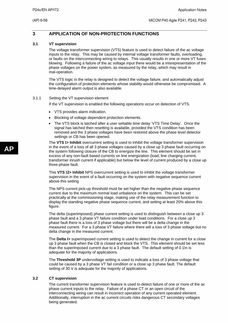
P24x/EN AP/I72
Application Notes (AP) 6-58 MiCOM P40 Agile P241, P242, P243
AP
3 APPLICATION OF NON-PROTECTION FUNCTIONS
3.1 VT supervision The voltage transformer supervision (VTS) feature is used to detect failure of the ac voltage inputs to the relay. This may be caused by internal voltage transformer faults, overloading, or faults on the interconnecting wiring to relays. This usually results in one or more VT fuses blowing. Following a failure of the ac voltage input there would be a misrepresentation of the phase voltages on the power system, as measured by the relay, which may result in mal-operation.
The VTS logic in the relay is designed to detect the voltage failure, and automatically adjust the configuration of protection elements whose stability would otherwise be compromised. A time-delayed alarm output is also available.
3.1.1 Setting the VT supervision element If the VT supervision is enabled the following operations occur on detection of VTS.
• VTS provides alarm indication. • Blocking of voltage dependent protection elements. • The VTS block is latched after a user settable time delay ‘VTS Time Delay’. Once the
signal has latched then resetting is available, provided the VTS condition has been removed and the 3 phase voltages have been restored above the phase level detector settings or CB has been opened.
The VTS Ι> Inhibit overcurrent setting is used to inhibit the voltage transformer supervision in the event of a loss of all 3 phase voltages caused by a close up 3 phase fault occurring on the system following closure of the CB to energize the line. This element should be set in excess of any non-fault based currents on line energization (load, line charging current, transformer inrush current if applicable) but below the level of current produced by a close up three-phase fault.
This VTS Ι2> Inhibit NPS overcurrent setting is used to inhibit the voltage transformer supervision in the event of a fault occurring on the system with negative sequence current above this setting
The NPS current pick-up threshold must be set higher than the negative phase sequence current due to the maximum normal load unbalance on the system. This can be set practically at the commissioning stage, making use of the relay measurement function to display the standing negative phase sequence current, and setting at least 20% above this figure.
The delta (superimposed) phase current setting is used to distinguish between a close up 3 phase fault and a 3 phase VT failure condition under load conditions. For a close up 3 phase fault there is a loss of 3 phase voltage but there will be a delta change in the measured current. For a 3 phase VT failure where there will a loss of 3 phase voltage but no delta change in the measured current.
The Delta I> superimposed current setting is used to detect the change in current for a close up 3 phase fault when the CB is closed and block the VTS. This element should be set less than the superimposed current due to a 3 phase fault. The default setting of 0.1In is adequate for the majority of applications.
The Threshold 3P undervoltage setting is used to indicate a loss of 3 phase voltage that could be caused by a 3 phase VT fail condition or a close up 3 phase fault. The default setting of 30 V is adequate for the majority of applications.
3.2 CT supervision The current transformer supervision feature is used to detect failure of one or more of the ac phase current inputs to the relay. Failure of a phase CT or an open circuit of the interconnecting wiring can result in incorrect operation of any current operated element. Additionally, interruption in the ac current circuits risks dangerous CT secondary voltages being generated.
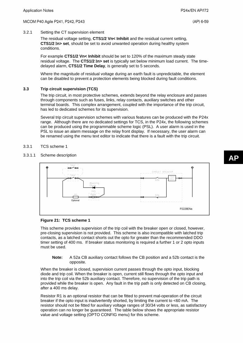
Application Notes
P24x/EN AP/I72 MiCOM P40 Agile P241, P242, P243 (AP) 6-59
AP
3.2.1 Setting the CT supervision element The residual voltage setting, CTS1/2 Vn< Inhibit and the residual current setting, CTS1/2 Ιn> set, should be set to avoid unwanted operation during healthy system conditions.
For example CTS1/2 Vn< Inhibit should be set to 120% of the maximum steady state residual voltage. The CTS1/2 Ιn> set is typically set below minimum load current. The time-delayed alarm, CTS1/2 Time Delay, is generally set to 5 seconds.
Where the magnitude of residual voltage during an earth fault is unpredictable, the element can be disabled to prevent a protection elements being blocked during fault conditions.
3.3 Trip circuit supervision (TCS) The trip circuit, in most protective schemes, extends beyond the relay enclosure and passes through components such as fuses, links, relay contacts, auxiliary switches and other terminal boards. This complex arrangement, coupled with the importance of the trip circuit, has led to dedicated schemes for its supervision.
Several trip circuit supervision schemes with various features can be produced with the P24x range. Although there are no dedicated settings for TCS, in the P24x, the following schemes can be produced using the programmable scheme logic (PSL). A user alarm is used in the PSL to issue an alarm message on the relay front display. If necessary, the user alarm can be renamed using the menu text editor to indicate that there is a fault with the trip circuit.
3.3.1 TCS scheme 1
3.3.1.1 Scheme description
P2228ENa
Optional
Figure 21: TCS scheme 1
This scheme provides supervision of the trip coil with the breaker open or closed, however, pre-closing supervision is not provided. This scheme is also incompatible with latched trip contacts, as a latched contact shorts out the opto for greater than the recommended DDO timer setting of 400 ms. If breaker status monitoring is required a further 1 or 2 opto inputs must be used.
Note: A 52a CB auxiliary contact follows the CB position and a 52b contact is the opposite.
When the breaker is closed, supervision current passes through the opto input, blocking diode and trip coil. When the breaker is open, current still flows through the opto input and into the trip coil via the 52b auxiliary contact. Therefore, no supervision of the trip path is provided while the breaker is open. Any fault in the trip path is only detected on CB closing, after a 400 ms delay.
Resistor R1 is an optional resistor that can be fitted to prevent mal-operation of the circuit breaker if the opto input is inadvertently shorted, by limiting the current to <60 mA. The resistor should not be fitted for auxiliary voltage ranges of 30/34 volts or less, as satisfactory operation can no longer be guaranteed. The table below shows the appropriate resistor value and voltage setting (OPTO CONFIG menu) for this scheme.
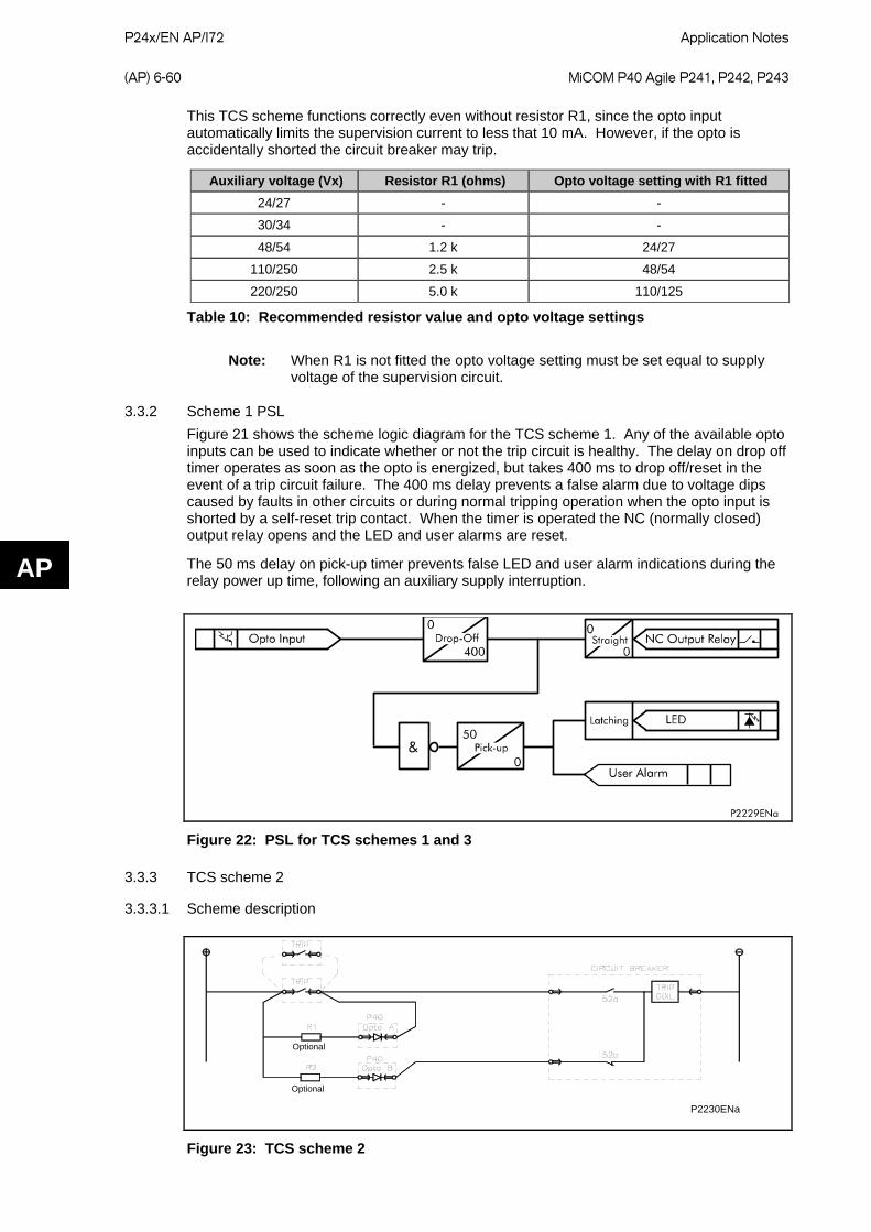
P24x/EN AP/I72
Application Notes (AP) 6-60 MiCOM P40 Agile P241, P242, P243
AP
This TCS scheme functions correctly even without resistor R1, since the opto input automatically limits the supervision current to less that 10 mA. However, if the opto is accidentally shorted the circuit breaker may trip.
Auxiliary voltage (Vx) Resistor R1 (ohms) Opto voltage setting with R1 fitted 24/27 - -
30/34 - -
48/54 1.2 k 24/27
110/250 2.5 k 48/54
220/250 5.0 k 110/125
Table 10: Recommended resistor value and opto voltage settings
Note: When R1 is not fitted the opto voltage setting must be set equal to supply voltage of the supervision circuit.
3.3.2 Scheme 1 PSL Figure 21 shows the scheme logic diagram for the TCS scheme 1. Any of the available opto inputs can be used to indicate whether or not the trip circuit is healthy. The delay on drop off timer operates as soon as the opto is energized, but takes 400 ms to drop off/reset in the event of a trip circuit failure. The 400 ms delay prevents a false alarm due to voltage dips caused by faults in other circuits or during normal tripping operation when the opto input is shorted by a self-reset trip contact. When the timer is operated the NC (normally closed) output relay opens and the LED and user alarms are reset.
The 50 ms delay on pick-up timer prevents false LED and user alarm indications during the relay power up time, following an auxiliary supply interruption.
Figure 22: PSL for TCS schemes 1 and 3
3.3.3 TCS scheme 2
3.3.3.1 Scheme description
P2230ENa
Optional
Optional
Figure 23: TCS scheme 2
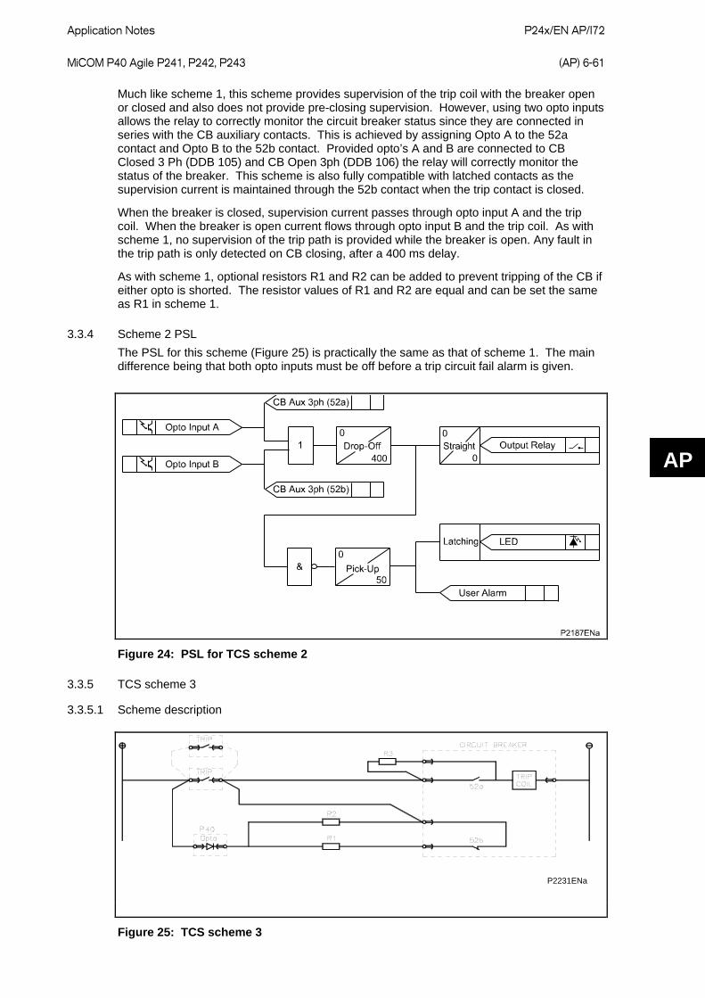
Application Notes
P24x/EN AP/I72 MiCOM P40 Agile P241, P242, P243 (AP) 6-61
AP
Much like scheme 1, this scheme provides supervision of the trip coil with the breaker open or closed and also does not provide pre-closing supervision. However, using two opto inputs allows the relay to correctly monitor the circuit breaker status since they are connected in series with the CB auxiliary contacts. This is achieved by assigning Opto A to the 52a contact and Opto B to the 52b contact. Provided opto’s A and B are connected to CB Closed 3 Ph (DDB 105) and CB Open 3ph (DDB 106) the relay will correctly monitor the status of the breaker. This scheme is also fully compatible with latched contacts as the supervision current is maintained through the 52b contact when the trip contact is closed.
When the breaker is closed, supervision current passes through opto input A and the trip coil. When the breaker is open current flows through opto input B and the trip coil. As with scheme 1, no supervision of the trip path is provided while the breaker is open. Any fault in the trip path is only detected on CB closing, after a 400 ms delay.
As with scheme 1, optional resistors R1 and R2 can be added to prevent tripping of the CB if either opto is shorted. The resistor values of R1 and R2 are equal and can be set the same as R1 in scheme 1.
3.3.4 Scheme 2 PSL The PSL for this scheme (Figure 25) is practically the same as that of scheme 1. The main difference being that both opto inputs must be off before a trip circuit fail alarm is given.
Figure 24: PSL for TCS scheme 2
3.3.5 TCS scheme 3
3.3.5.1 Scheme description
P2231ENa
Figure 25: TCS scheme 3
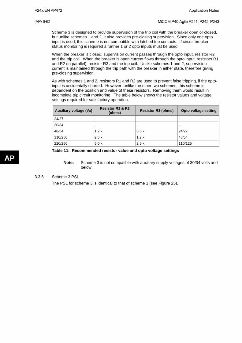
P24x/EN AP/I72
Application Notes (AP) 6-62 MiCOM P40 Agile P241, P242, P243
AP
Scheme 3 is designed to provide supervision of the trip coil with the breaker open or closed, but unlike schemes 1 and 2, it also provides pre-closing supervision. Since only one opto input is used, this scheme is not compatible with latched trip contacts. If circuit breaker status monitoring is required a further 1 or 2 opto inputs must be used.
When the breaker is closed, supervision current passes through the opto input, resistor R2 and the trip coil. When the breaker is open current flows through the opto input, resistors R1 and R2 (in parallel), resistor R3 and the trip coil. Unlike schemes 1 and 2, supervision current is maintained through the trip path with the breaker in either state, therefore giving pre-closing supervision.
As with schemes 1 and 2, resistors R1 and R2 are used to prevent false tripping, if the opto-input is accidentally shorted. However, unlike the other two schemes, this scheme is dependent on the position and value of these resistors. Removing them would result in incomplete trip circuit monitoring. The table below shows the resistor values and voltage settings required for satisfactory operation.
Auxiliary voltage (Vx) Resistor R1 & R2 (ohms) Resistor R3 (ohms) Opto voltage setting
24/27 - - -
30/34 - - -
48/54 1.2 k 0.6 k 24/27
110/250 2.5 k 1.2 k 48/54
220/250 5.0 k 2.5 k 110/125
Table 11: Recommended resistor value and opto voltage settings
Note: Scheme 3 is not compatible with auxiliary supply voltages of 30/34 volts and below.
3.3.6 Scheme 3 PSL The PSL for scheme 3 is identical to that of scheme 1 (see Figure 25).
Application Notes
P24x/EN AP/I72 MiCOM P40 Agile P241, P242, P243 (AP) 6-63
AP
4 CURRENT TRANSFORMER REQUIREMENTS The current transformer requirements for each current input depend on the protection function with which they are related and whether the line current transformers are being shared with other current inputs. Where current transformers are being shared by multiple current inputs, the kneepoint voltage requirements should be calculated for each input and the highest calculated value used.
The CT requirements for the P24x protection functions except the current differential are shown below. The P243 is the only model which includes differential protection and for this relay the highest calculated value from the general protection and differential protection CT requirements should be used. The differential CT requirements are shown in Table 12.
The general current transformer requirements are based on a maximum prospective fault current of 50 times the relay rated current (In) and the relay having an instantaneous setting of 25 times rated current (In). The current transformer requirements are designed to provide operation of all protection elements except the differential protection.
Where the criteria for a specific application are in excess of those detailed above, or the actual lead resistance exceeds the limiting value quoted, the CT requirements may need to be increased according to the formulae in sections 4.2/3/4.
Nominal rating Nominal output Accuracy class Accuracy limited factor
Limiting lead resistance
1 A 2.5 VA 10P 20 1.3 ohms
5 A 7.5 VA 10P 20 0.11 ohms
Table 12: The CT requirements for the P24x protection functions excluding differential protection
4.1 Motor differential function (P243)
4.1.1 Biased differential protection The kneepoint voltage requirements for the current transformers used for the current inputs of the motor differential function based on settings of Ιs1 = 0.05 Ιn, k1 = 0%, Ιs2 = 1.2 Ιn, k2 = 150%, and with a boundary condition of starting current ≤ 10Ιn, are:
Where the motor is not earthed or resistance earthed at the motor neutral point then the CT knee point voltage requirements are:
Vk ≥ 30Ιn (Rct + RL + Rr) with a minimum of 60Ιn
Where the motor is solidly earthed at the motor neutral point then the CT knee point voltage requirements are:
Vk ≥ 40Ιn (Rct + 2RL + Rr) with a minimum of 60Ιn
Where
Vk = Minimum current transformer kneepoint voltage for through fault stability.
Ιn = Relay rated current.
Rct = Resistance of current transformer secondary winding (Ω).
RL = Resistance of a single lead from relay to current transformer (Ω).
Rr = Resistance of any other protective relays sharing the current transformer (Ω).

P24x/EN AP/I72
Application Notes (AP) 6-64 MiCOM P40 Agile P241, P242, P243
AP
For Class-X current transformers, the excitation current at the calculated kneepoint voltage requirement should be less than 2.5Ιn (<5% of the maximum perspective fault current 50 Ιn, on which these CT requirements are based). For IEC standard protection class current transformers, it should be ensured that class 5P are used.
High impedance differential protection
If the motor differential protection function is used to implement high impedance differential protection, then the current transformer requirements are as follows:
Rs = [1.5 x (Ιf) * (RCT + 2RL)] /ΙS1
VK ≥ 2 x Ιs1 * Rs
Where
Rs = Value of stabilizing resistor (ohms)
Ιf = Maximum starting current (amps)
VK = CT knee point voltage (volts)
ΙS1 = Current setting of differential element (amps)
RCT = Resistance of current transformer secondary winding (ohms)
RL = Resistance of a single lead from relay to current transformer (ohms)
Self Balanced differential protection
If the motor differential protection function is used to implement self balanced differential protection, then the current transformer requirements are as follows:
VK ≥ (1.5 x If x (RCT + 2RL))/IS
Where
Ιf = Maximum starting current (amps)
VK = CT knee point voltage (volts)
ΙS = Current setting of differential element (amps)
RCT = Resistance of current transformer secondary winding (ohms)
RL = Resistance of a single lead from relay to current transformer (ohms)
4.2 Non-directional definite time/IDMT short circuit and definite time/IDMT derived earth fault protection
4.2.1 Definite time/IDMT delayed short circuit elements VK ≥ Icp/2 x (RCT + RL + Rrp)
4.2.2 Definite time delayed/IDMT derived earth fault elements VK ≥ Icn/2 x (RCT + 2RL + Rrp + Rrn)
4.3 Non-directional instantaneous short circuit and derived earth fault protection
4.3.1 Instantaneous short circuit elements VK ≥ Isp x (RCT + RL + Rrp)
4.3.2 Instantaneous derived earth fault elements VK ≥ Isn x (RCT + 2RL + Rrp + Rrn)

Application Notes
P24x/EN AP/I72 MiCOM P40 Agile P241, P242, P243 (AP) 6-65
AP
4.4 Directional definite time/IDMT derived earth fault protection
4.4.1 Directional time delayed derived earth fault protection VK ≥ Icn/2 x (RCT + 2RL + Rrp + Rrn)
4.4.2 Directional instantaneous derived earth fault protection VK ≥ Ifn/2 x (RCT + 2RL + Rrp + Rrn)
4.5 Non-directional/directional definite time/IDMT sensitive earth fault (SEF) protection
4.5.1 Non-directional time delayed SEF protection (residually connected) VK ≥ Icn/2 x (RCT + 2RL + Rrp + Rrn)
4.5.2 Non-directional instantaneous SEF protection (residually connected) VK ≥ Isn/2 x (RCT + 2RL + Rrp + Rrn)
4.5.3 Directional time delayed SEF protection (residually connected) VK ≥ Icn/2 x (RCT + 2RL + Rrp + Rrn)
4.5.4 Directional instantaneous SEF protection (residually connected) VK ≥ Ifn/2 x (RCT + 2RL + Rrp + Rrn)
4.5.5 SEF protection - as fed from a core-balance CT Core balance current transformers of metering class accuracy are required and should have a limiting secondary voltage satisfying the formulae given below:
Directional non-directional time delayed element:
VK ≥ Icn/2 x (RCT + 2RL + Rrn)
Directional instantaneous element:
VK ≥ Ifn/2 x (RCT + 2RL + Rrn)
Non-directional instantaneous element
VK ≥ Isn/2 x (RCT + 2RL + Rrn)
Note: In addition, it should be ensured that the phase error of the applied core balance current transformer is less than 90 minutes at 10% of rated current and less than 150 minutes at 1% of rated current.
Abbreviations used in the previous formulae are explained below:
Where
VK = Required CT knee-point voltage (volts)
Ifn = Maximum prospective secondary earth fault current (amps)
Ifp = Maximum prospective secondary phase fault current (amps)
Icn = Maximum prospective secondary earth fault current or 31 times I> setting (whichever is lower) (amps)
Icp = Maximum prospective secondary phase fault current or 31 times I> setting (whichever is lower) (amps)
Isn = Stage 2 Earth Fault setting (amps)
Isp = Stage 2 setting (amps)
RCT = Resistance of current transformer secondary winding (ohms)
RL = Resistance of a single lead from relay to current transformer (ohms)

P24x/EN AP/I72
Application Notes (AP) 6-66 MiCOM P40 Agile P241, P242, P243
AP
Rrp = Impedance of relay phase current input at 30 In (ohms)
Rrn = Impedance of the relay neutral current input at 30 In (ohms)
4.6 Converting an IEC185 current transformer standard protection classification to a kneepoint voltage The suitability of an IEC standard protection class current transformer can be checked against the kneepoint voltage requirements specified previously.
For example, if the available current transformers have a 15 VA 5P 10 designation, then an estimated kneepoint voltage can be obtained as follows:
Vk = VA x ALF
Ιn + ALF x Ιn x Rct
Where:
Vk = Required kneepoint voltage
VA = Current transformer rated burden (VA)
ALF = Accuracy limit factor
Ιn = Current transformer secondary rated current (A)
Rct = Resistance of current transformer secondary winding (Ω)
If Rct is not available, then the second term in the above equation can be ignored.
Example: 400/5A, 15VA 5P 10, Rct = 0.2Ω
Vk = 15 x 10
5 + 10 x 5 x 0.2
= 40 V
4.7 Converting IEC185 current transformer standard protection classification to an ANSI/IEEE standard voltage rating MiCOM Px40 series protection is compatible with ANSI/IEEE current transformers as specified in the IEEE C57.13 standard. The applicable class for protection is class "C", which specifies a non air-gapped core. The CT design is identical to IEC class P, or British Standard class X, but the rating is specified differently.
The ANSI/IEEE “C” Class standard voltage rating required is lower than an IEC knee point voltage. This is because the ANSI/IEEE voltage rating is defined in terms of useful output voltage at the terminals of the CT, whereas the IEC knee point voltage includes the voltage drop across the internal resistance of the CT secondary winding added to the useful output. The IEC/BS knee point is also typically 5% higher than the ANSI/IEEE knee point.
Therefore:
Vc = [ Vk .- Internal voltage drop ] / 1.05
= [ Vk - (In . RCT . ALF) ] / 1.05
Where:
Vc = “C” Class standard voltage rating
Vk = IEC Knee point voltage required
Ιn = CT rated current = 5 A in USA
RCT = CT secondary winding resistance
(for 5 A CTs, the typical resistance is 0.002 ohms/secondary turn)

Application Notes
P24x/EN AP/I72 MiCOM P40 Agile P241, P242, P243 (AP) 6-67
AP
ALF = The CT accuracy limit factor, the rated dynamic current output of a "C" class CT (Kssc) is always 20 x In
The IEC accuracy limit factor is identical to the 20 times secondary current ANSI/IEEE rating.
Therefore:
Vc = [ Vk - (100 . RCT ) ] / 1.05

P24x/EN AP/I72
Application Notes (AP) 6-68 MiCOM P40 Agile P241, P242, P243
AP
5 READ ONLY MODE With IEC 61850 and Ethernet / Internet communication capabilities, security has become a pressing issue. The Px40 relay provides a facility to allow the user to enable or disable the change in configuration remotely.
Read Only mode can be enabled/disabled for the following rear ports:
• Rear Port 1 – IEC 60870-5-103 and Courier protocols • Rear Port 2 (if fitted) – Courier protocol • Ethernet Port (if fitted) – Courier protocol (“tunnelled”)
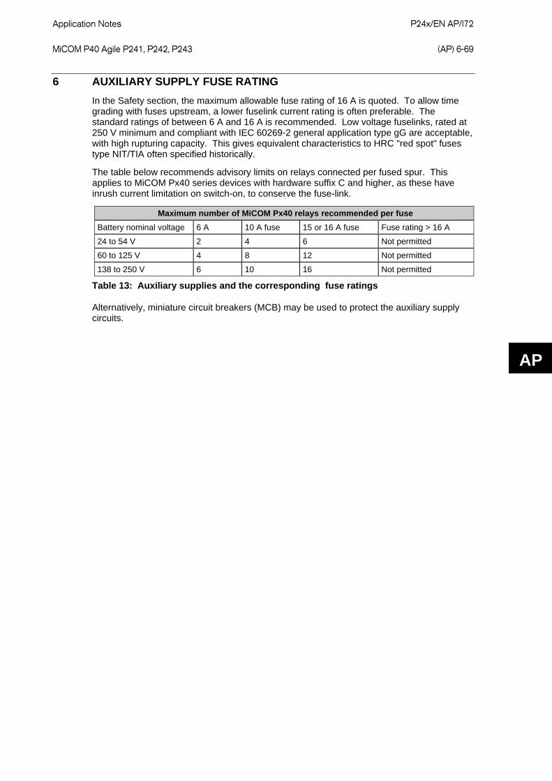
Application Notes
P24x/EN AP/I72 MiCOM P40 Agile P241, P242, P243 (AP) 6-69
AP
6 AUXILIARY SUPPLY FUSE RATING In the Safety section, the maximum allowable fuse rating of 16 A is quoted. To allow time grading with fuses upstream, a lower fuselink current rating is often preferable. The standard ratings of between 6 A and 16 A is recommended. Low voltage fuselinks, rated at 250 V minimum and compliant with IEC 60269-2 general application type gG are acceptable, with high rupturing capacity. This gives equivalent characteristics to HRC "red spot" fuses type NIT/TIA often specified historically.
The table below recommends advisory limits on relays connected per fused spur. This applies to MiCOM Px40 series devices with hardware suffix C and higher, as these have inrush current limitation on switch-on, to conserve the fuse-link.
Maximum number of MiCOM Px40 relays recommended per fuse Battery nominal voltage 6 A 10 A fuse 15 or 16 A fuse Fuse rating > 16 A
24 to 54 V 2 4 6 Not permitted
60 to 125 V 4 8 12 Not permitted
138 to 250 V 6 10 16 Not permitted
Table 13: Auxiliary supplies and the corresponding fuse ratings
Alternatively, miniature circuit breakers (MCB) may be used to protect the auxiliary supply circuits.

P24x/EN AP/I72
Application Notes (AP) 6-70 MiCOM P40 Agile P241, P242, P243
AP

Programmable Logic
P24x/EN PL/I72 MiCOM P40 Agile P241, P242, P243 (PL) 7-1
PL PROGRAMMABLE LOGIC

P24x/EN PL/I72
Programmable Logic (PL) 7-2 MiCOM P40 Agile P241, P242, P243
PL

Programmable Logic
P24x/EN PL/I72 MiCOM P40 Agile P241, P242, P243 (PL) 7-3
PL
CONTENTS
1 PROGRAMMABLE LOGIC 5
1.1 Overview 5
1.2 MiCOM S1 Studio Px40 PSL editor 5
1.3 How to use MiCOM Px40 PSL editor 6
1.4 Warnings 6
1.5 Toolbar and commands 6
1.5.1 Standard tools 6
1.5.2 Alignment tools 6
1.5.3 Drawing tools 6
1.5.4 Nudge tools 7
1.5.5 Rotation tools 7
1.5.6 Structure tools 7
1.5.7 Zoom and pan tools 7
1.5.8 Logic symbols 7
1.6 PSL logic signals properties 8
1.6.1 Link properties 9
1.6.2 Opto signal properties 9
1.6.3 Input signal properties 9
1.6.4 Output signal properties 9
1.6.5 GOOSE input signal properties 10
1.6.6 GOOSE output signal properties 10
1.6.7 Control input signal properties 10
1.6.8 Function key properties (P242/3 only) 10
1.6.9 Fault recorder trigger properties 11
1.6.10 LED signal properties 11
1.6.11 Contact signal properties 11
1.6.12 LED conditioner properties 11
1.6.12.1 Tri-color LED conditioner (P242/3) 11
1.6.12.2 Red LED conditioner (P241) 12
1.6.13 Contact conditioner properties 12
1.6.14 Timer properties 12
1.6.15 Gate properties 13
1.7 Description of logic nodes 13
1.8 Factory default programmable scheme logic 22
1.9 Logic input mapping 22
1.10 Relay output contact mapping 23
1.11 Programmable LED output mapping 24
1.12 Fault recorder start mapping 25
P24x/EN PL/I72
Programmable Logic (PL) 7-4 MiCOM P40 Agile P241, P242, P243
PL
2 MICOM P24X PROGRAMMABLE SCHEME LOGIC 26
FIGURES Figure 1: Tri-color LED conditioning (P242/3) 11
Figure 2: P241 Opto Input Mappings 26
Figure 3: P241 Output Relay Mappings 27
Figure 4: P241 LED Mappings 28
Figure 5: Fault Recorder Trigger Mapping 29
Figure 6: P242/3 Opto Input Mappings 29
Figure 7: P242/3 Output Relay Mappings 30
Figure 8: P242/3 LED Mappings 31
Figure 9: Fault Recorder Trigger Mapping 32
Figure 10: Function Key Mapping 32
TABLES Table 1: Description of available logic nodes 22
Table 2: Default settings 22
Table 3: P241 opto inputs default mappings 23
Table 4: P242/3 opto inputs default mappings 23
Table 5: P241 relay output contacts default mappings 23
Table 6: P242/3 relay output contacts default mappings 24
Table 7: P241 programmable LED default mappings 24
Table 8: P242/3 programmable LED default mappings 25
Table 9: Default fault record initiation 25

Programmable Logic
P24x/EN PL/I72 MiCOM P40 Agile P241, P242, P243 (PL) 7-5
PL
1 PROGRAMMABLE LOGIC
1.1 Overview The purpose of the programmable scheme logic (PSL) is to allow the relay user to configure an individual protection scheme to suit their own particular application. This is achieved through the use of programmable logic gates and delay timers.
The input to the PSL is any combination of the status of opto inputs. It is also used to assign the mapping of functions to the opto inputs and output contacts, the outputs of the protection elements, such as protection starts and trips, and the outputs of the fixed protection scheme logic. The fixed scheme logic provides the relay’s standard protection schemes. The PSL consists of software logic gates and timers. The logic gates can be programmed to perform a range of different logic functions and can accept any number of inputs. The timers are used either to create a programmable delay, and/or to condition the logic outputs, e.g. to create a pulse of fixed duration on the output regardless of the length of the pulse on the input. The outputs of the PSL are the LEDs on the front panel of the relay and the output contacts at the rear.
The execution of the PSL logic is event driven; the logic is processed whenever any of its inputs change, for example as a result of a change in one of the digital input signals or a trip output from a protection element. Also, only the part of the PSL logic that is affected by the particular input change that has occurred is processed. This reduces the amount of processing time that is used by the PSL; even with large, complex PSL schemes the relay trip time will not lengthen.
This system provides flexibility for the user to create their own scheme logic design. However, it also means that the PSL can be configured into a very complex system; therefore setting of the PSL is implemented through the PC support package MiCOM S1 Studio.
1.2 MiCOM S1 Studio Px40 PSL editor To access the Px40 PSL Editor menu click on
The PSL editors enable you to connect to any MiCOM device front port, retrieve and edit its Programmable Scheme Logic files and send the modified file back to a MiCOM Px40 device.
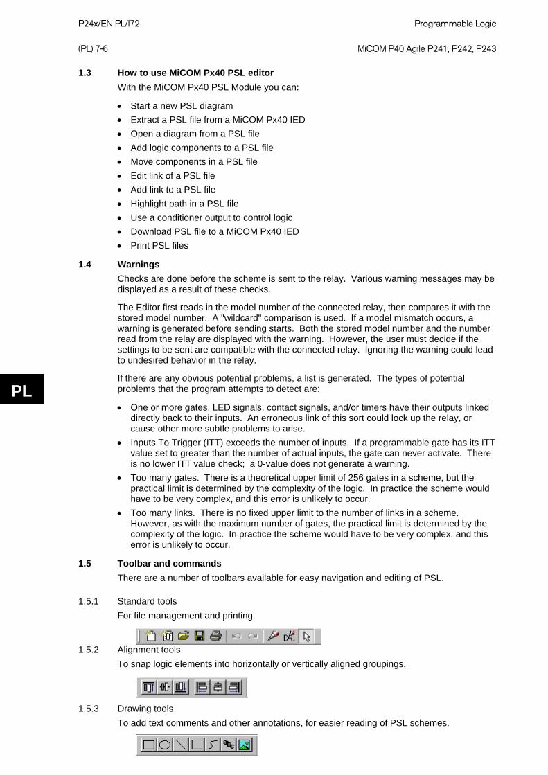
P24x/EN PL/I72
Programmable Logic (PL) 7-6 MiCOM P40 Agile P241, P242, P243
PL
1.3 How to use MiCOM Px40 PSL editor With the MiCOM Px40 PSL Module you can:
• Start a new PSL diagram • Extract a PSL file from a MiCOM Px40 IED • Open a diagram from a PSL file • Add logic components to a PSL file • Move components in a PSL file • Edit link of a PSL file • Add link to a PSL file • Highlight path in a PSL file • Use a conditioner output to control logic • Download PSL file to a MiCOM Px40 IED • Print PSL files
1.4 Warnings Checks are done before the scheme is sent to the relay. Various warning messages may be displayed as a result of these checks.
The Editor first reads in the model number of the connected relay, then compares it with the stored model number. A "wildcard" comparison is used. If a model mismatch occurs, a warning is generated before sending starts. Both the stored model number and the number read from the relay are displayed with the warning. However, the user must decide if the settings to be sent are compatible with the connected relay. Ignoring the warning could lead to undesired behavior in the relay.
If there are any obvious potential problems, a list is generated. The types of potential problems that the program attempts to detect are:
• One or more gates, LED signals, contact signals, and/or timers have their outputs linked directly back to their inputs. An erroneous link of this sort could lock up the relay, or cause other more subtle problems to arise.
• Inputs To Trigger (ITT) exceeds the number of inputs. If a programmable gate has its ITT value set to greater than the number of actual inputs, the gate can never activate. There is no lower ITT value check; a 0-value does not generate a warning.
• Too many gates. There is a theoretical upper limit of 256 gates in a scheme, but the practical limit is determined by the complexity of the logic. In practice the scheme would have to be very complex, and this error is unlikely to occur.
• Too many links. There is no fixed upper limit to the number of links in a scheme. However, as with the maximum number of gates, the practical limit is determined by the complexity of the logic. In practice the scheme would have to be very complex, and this error is unlikely to occur.
1.5 Toolbar and commands There are a number of toolbars available for easy navigation and editing of PSL.
1.5.1 Standard tools For file management and printing.
1.5.2 Alignment tools To snap logic elements into horizontally or vertically aligned groupings.
1.5.3 Drawing tools To add text comments and other annotations, for easier reading of PSL schemes.
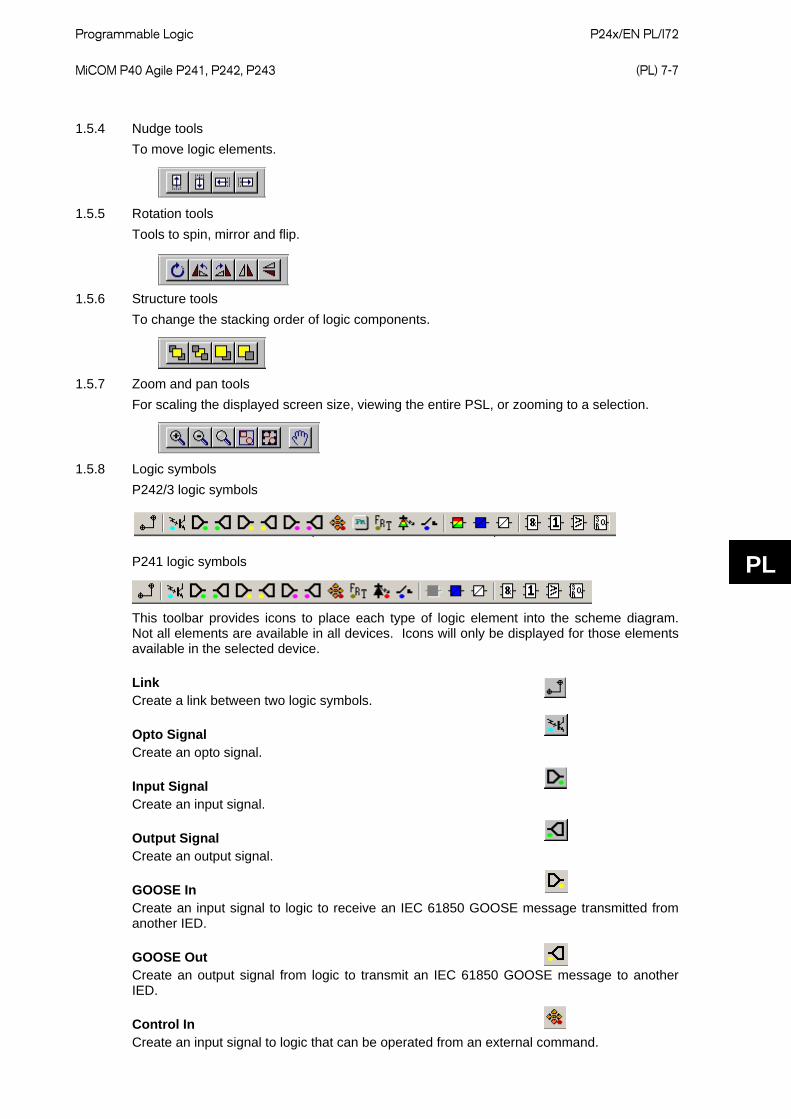
Programmable Logic
P24x/EN PL/I72 MiCOM P40 Agile P241, P242, P243 (PL) 7-7
PL
1.5.4 Nudge tools To move logic elements.
1.5.5 Rotation tools Tools to spin, mirror and flip.
1.5.6 Structure tools To change the stacking order of logic components.
1.5.7 Zoom and pan tools For scaling the displayed screen size, viewing the entire PSL, or zooming to a selection.
1.5.8 Logic symbols P242/3 logic symbols
P241 logic symbols
This toolbar provides icons to place each type of logic element into the scheme diagram. Not all elements are available in all devices. Icons will only be displayed for those elements available in the selected device.
Link Create a link between two logic symbols.
Opto Signal Create an opto signal.
Input Signal Create an input signal.
Output Signal Create an output signal.
GOOSE In Create an input signal to logic to receive an IEC 61850 GOOSE message transmitted from another IED.
GOOSE Out Create an output signal from logic to transmit an IEC 61850 GOOSE message to another IED.
Control In Create an input signal to logic that can be operated from an external command.
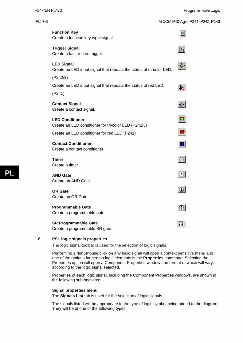
P24x/EN PL/I72
Programmable Logic (PL) 7-8 MiCOM P40 Agile P241, P242, P243
PL
Function Key Create a function key input signal.
Trigger Signal Create a fault record trigger.
LED Signal Create an LED input signal that repeats the status of tri-color LED.
(P242/3)
Create an LED input signal that repeats the status of red LED.
(P241)
Contact Signal Create a contact signal.
LED Conditioner Create an LED conditioner for tri-color LED (P242/3)
Create an LED conditioner for red LED (P241)
Contact Conditioner Create a contact conditioner.
Timer Create a timer.
AND Gate Create an AND Gate.
OR Gate Create an OR Gate.
Programmable Gate Create a programmable gate.
SR Programmable Gate Create a programmable SR gate.
1.6 PSL logic signals properties The logic signal toolbar is used for the selection of logic signals.
Performing a right-mouse click on any logic signal will open a context sensitive menu and one of the options for certain logic elements is the Properties command. Selecting the Properties option will open a Component Properties window, the format of which will vary according to the logic signal selected.
Properties of each logic signal, including the Component Properties windows, are shown in the following sub-sections:
Signal properties menu The Signals List tab is used for the selection of logic signals.
The signals listed will be appropriate to the type of logic symbol being added to the diagram. They will be of one of the following types:
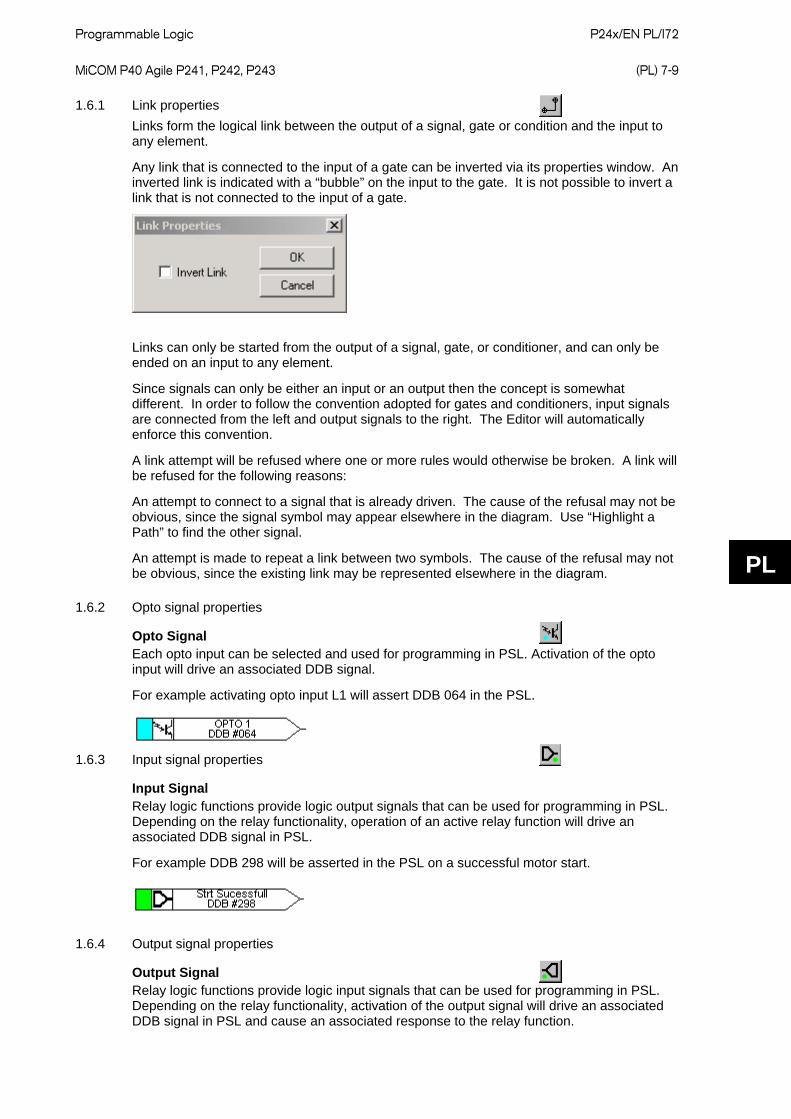
Programmable Logic
P24x/EN PL/I72 MiCOM P40 Agile P241, P242, P243 (PL) 7-9
PL
1.6.1 Link properties Links form the logical link between the output of a signal, gate or condition and the input to any element.
Any link that is connected to the input of a gate can be inverted via its properties window. An inverted link is indicated with a “bubble” on the input to the gate. It is not possible to invert a link that is not connected to the input of a gate.
Rules For Linking Symbols
Links can only be started from the output of a signal, gate, or conditioner, and can only be ended on an input to any element.
Since signals can only be either an input or an output then the concept is somewhat different. In order to follow the convention adopted for gates and conditioners, input signals are connected from the left and output signals to the right. The Editor will automatically enforce this convention.
A link attempt will be refused where one or more rules would otherwise be broken. A link will be refused for the following reasons:
An attempt to connect to a signal that is already driven. The cause of the refusal may not be obvious, since the signal symbol may appear elsewhere in the diagram. Use “Highlight a Path” to find the other signal.
An attempt is made to repeat a link between two symbols. The cause of the refusal may not be obvious, since the existing link may be represented elsewhere in the diagram.
1.6.2 Opto signal properties
Opto Signal Each opto input can be selected and used for programming in PSL. Activation of the opto input will drive an associated DDB signal.
For example activating opto input L1 will assert DDB 064 in the PSL.
1.6.3 Input signal properties
Input Signal Relay logic functions provide logic output signals that can be used for programming in PSL. Depending on the relay functionality, operation of an active relay function will drive an associated DDB signal in PSL.
For example DDB 298 will be asserted in the PSL on a successful motor start.
1.6.4 Output signal properties
Output Signal Relay logic functions provide logic input signals that can be used for programming in PSL. Depending on the relay functionality, activation of the output signal will drive an associated DDB signal in PSL and cause an associated response to the relay function.
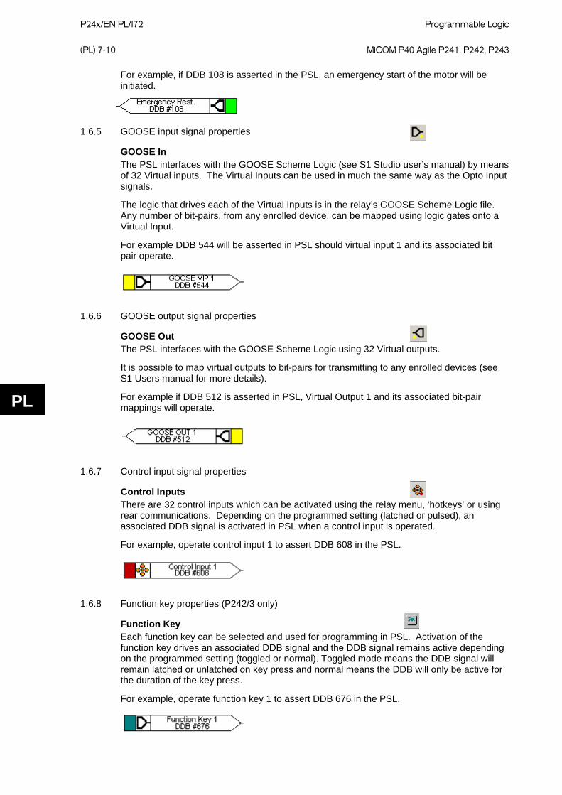
P24x/EN PL/I72
Programmable Logic (PL) 7-10 MiCOM P40 Agile P241, P242, P243
PL
For example, if DDB 108 is asserted in the PSL, an emergency start of the motor will be initiated.
1.6.5 GOOSE input signal properties
GOOSE In The PSL interfaces with the GOOSE Scheme Logic (see S1 Studio user’s manual) by means of 32 Virtual inputs. The Virtual Inputs can be used in much the same way as the Opto Input signals.
The logic that drives each of the Virtual Inputs is in the relay’s GOOSE Scheme Logic file. Any number of bit-pairs, from any enrolled device, can be mapped using logic gates onto a Virtual Input.
For example DDB 544 will be asserted in PSL should virtual input 1 and its associated bit pair operate.
1.6.6 GOOSE output signal properties
GOOSE Out The PSL interfaces with the GOOSE Scheme Logic using 32 Virtual outputs.
It is possible to map virtual outputs to bit-pairs for transmitting to any enrolled devices (see S1 Users manual for more details).
For example if DDB 512 is asserted in PSL, Virtual Output 1 and its associated bit-pair mappings will operate.
1.6.7 Control input signal properties
Control Inputs There are 32 control inputs which can be activated using the relay menu, ‘hotkeys’ or using rear communications. Depending on the programmed setting (latched or pulsed), an associated DDB signal is activated in PSL when a control input is operated.
For example, operate control input 1 to assert DDB 608 in the PSL.
1.6.8 Function key properties (P242/3 only)
Function Key Each function key can be selected and used for programming in PSL. Activation of the function key drives an associated DDB signal and the DDB signal remains active depending on the programmed setting (toggled or normal). Toggled mode means the DDB signal will remain latched or unlatched on key press and normal means the DDB will only be active for the duration of the key press.
For example, operate function key 1 to assert DDB 676 in the PSL.
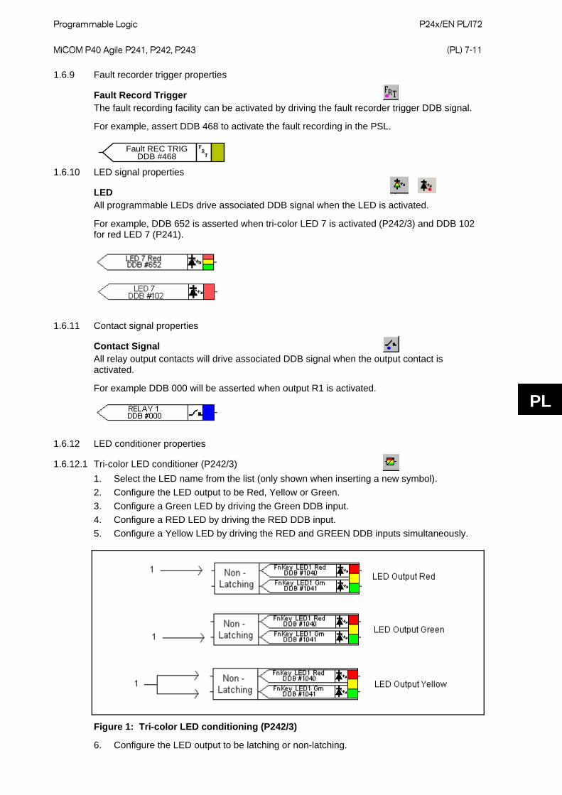
Programmable Logic
P24x/EN PL/I72 MiCOM P40 Agile P241, P242, P243 (PL) 7-11
PL
1.6.9 Fault recorder trigger properties
Fault Record Trigger The fault recording facility can be activated by driving the fault recorder trigger DDB signal.
For example, assert DDB 468 to activate the fault recording in the PSL.
1.6.10 LED signal properties
LED All programmable LEDs drive associated DDB signal when the LED is activated.
For example, DDB 652 is asserted when tri-color LED 7 is activated (P242/3) and DDB 102 for red LED 7 (P241).
1.6.11 Contact signal properties
Contact Signal All relay output contacts will drive associated DDB signal when the output contact is activated.
For example DDB 000 will be asserted when output R1 is activated.
1.6.12 LED conditioner properties
1.6.12.1 Tri-color LED conditioner (P242/3) 1. Select the LED name from the list (only shown when inserting a new symbol). 2. Configure the LED output to be Red, Yellow or Green. 3. Configure a Green LED by driving the Green DDB input. 4. Configure a RED LED by driving the RED DDB input. 5. Configure a Yellow LED by driving the RED and GREEN DDB inputs simultaneously.
Figure 1: Tri-color LED conditioning (P242/3)
6. Configure the LED output to be latching or non-latching.
Fault REC TRIG
DDB #468

P24x/EN PL/I72
Programmable Logic (PL) 7-12 MiCOM P40 Agile P241, P242, P243
PL
1.6.12.2 Red LED conditioner (P241) 1. Select the LED name from the list (only shown when inserting a new symbol). 2. Configure the LED output to be latching or non-latching
1.6.13 Contact conditioner properties Each contact can be conditioned with an associated timer that can be selected for pick up, drop off, dwell, pulse, pick-up/drop-off, straight-through, or latching operation.
Straight-through means it is not conditioned at all whereas Latching is used to create a sealed-in or lockout type function.
1. Select the contact name from the Contact Name list (only shown when inserting a new
symbol). 2. Choose the conditioner type required in the Mode tick list. 3. Set the Pick-up Time (in milliseconds), if required. 4. Set the Drop-off Time (in milliseconds), if required.
1.6.14 Timer properties Each timer can be selected for pick up, drop off, dwell, pulse or pick-up/drop-off operation.
1. Choose the operation mode from the Timer Mode tick list. 2. Set the Pick-up Time (in milliseconds), if required. 3. Set the Drop-off Time (in milliseconds), if required.

Programmable Logic
P24x/EN PL/I72 MiCOM P40 Agile P241, P242, P243 (PL) 7-13
PL
1.6.15 Gate properties A Gate may be an AND, OR, or programmable gate.
An AND gate requires that all inputs are TRUE for the output to be TRUE.
An OR gate requires that one or more input is TRUE for the output to be TRUE.
A Programmable gate requires that the number of inputs that are TRUE is equal to or greater than its ‘Inputs to Trigger’ setting for the output to be TRUE.
1. Select the Gate type AND, OR, or Programmable. 2. Set the number of inputs to trigger when Programmable is selected. 3. Select if the output of the gate should be inverted using the Invert Output check box. An
inverted output is indicated with a "bubble" on the gate output.
1.7 Description of logic nodes DDB no. English text Source Description
0 Relay 1 (Output Label Setting) Relay conditioner Relay 1 is on
6 Relay 7 (Output Label Setting) Relay conditioner Relay 7 is on
15 Relay 16 (Output Label Setting) Relay conditioner Relay 16 is on (P242/3 only)
16 to 63 Not Used
64 Opto 1 (Input Label Setting) Opto Isolator Input Opto 1 is on
71 Opto 8 (Input Label Setting) Opto Isolator Input Opto 8 is on
79 Opto 16 (Input Setting) Opto Isolator Input Opto 16 is on (P242/3 only)
96 LED1 Red PSL LED 1 Red is on (P241 only)
103 LED8 Red. PSL LED 8 Red is on (P241 only)
104 Speed Input PSL Speed Switch input is on
105 CB Aux 3Ph - 52A PSL CB1 Closed
106 CB Aux 3Ph - 52B PSL CB1 Open
107 Setting Group. PSL Setting Group change (Off = Group1, On = Group 2)
108 Emergency Rest. PSL Initiates Emergency Restart of motor
109 Reset Thermal PSL Resets Thermal State to 0%

P24x/EN PL/I72
Programmable Logic (PL) 7-14 MiCOM P40 Agile P241, P242, P243
PL
DDB no. English text Source Description 110 Dist Rec Trig PSL Triggers the Disturbance Recorder
111 Close PSL Initiates a breaker close command
112 Trip PSL Initiates a breaker trip command
113 Reset Latches PSL Reset all latched LEDs and output relays
114 Test Mode PSL
Commissioning Tests - automatically places relay in Test Mode which takes the relay out of service and allows secondary injection testing of the relay. For IEC 60870-5-103 protocol spontaneous events and cyclic measured data transmitted whilst the relay is in test mode will have a COT of ‘test mode’
115 External Trip PSL External Trip 3 phase - allows external protection to initiate breaker fail and circuit breaker condition monitoring counters.
116 Time Synch PSL Time Synchronism by opto Input pulse
117 FFail Block PSL Blocks operation of the Field Failure protection
118 Trip LED PSL Signal to switch on the Trip LED
119 MCB/VTS PSL VT supervision input - signal from external Miniature Circuit Breaker showing MCB tripped
120 Monitor Blocking DDB PSL Monitor Blocking DDB
121 Command Blocking DDB PSL Command Blocking DDB
122 RP1 Read Only DDB PSL Rear communications Port 1 read only mode selection
123 RP2 Read Only DDB PSL Rear communications Port 1 read only mode selection
124 NIC Read Only DDB PSL Rear Ethernet communications port read only mode selection
125 V2>1 Timer Block PSL Block 1st stage Negative Phase Sequence Overvoltage Timer
126 V2>1 Inhibit PSL Inhibit 1st stage Negative Phase Sequence Overvoltage
127 V2>2 Timer Block PSL Block 2nd stage Negative Phase Sequence Overvoltage Timer
128 V2>2 Inhibit PSL Inhibit 2nd stage Negative Phase Sequence Overvoltage
129 V<1 Timer Block PSL Block 1st stage Undervoltage Timer
130 V<1 Inhibit PSL Inhibit 1st stage Undervoltage
131 V<2 Timer Block PSL Block 2nd stage Undervoltage Timer
132 V<2 Inhibit PSL Inhibit 2nd stage Undervoltage
133 I>1 Timer Block PSL Block 1st stage Overcurrent Timer
134 I>1 Inhibit PSL Inhibit 1st stage Overcurrent
135 I>2 Timer Block PSL Block 2nd stage Overcurrent Timer
136 I>2 Inhibit PSL Inhibit 2nd stage Overcurrent
137 I>3 Timer Block PSL Block 3rd stage Overcurrent Timer
138 I>3 Inhibit PSL Inhibit 3rd stage Overcurrent
139 I>4 Timer Block PSL Block 4th stage Overcurrent Timer
140 I>4 Inhibit PSL Inhibit 4th stage Overcurrent
141 to 173 Not Used
174 General Alarm Any Alarm is operated
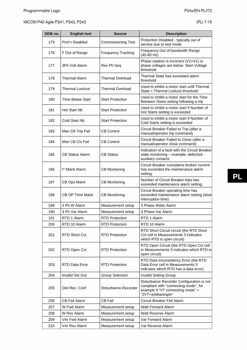
Programmable Logic
P24x/EN PL/I72 MiCOM P40 Agile P241, P242, P243 (PL) 7-15
PL
DDB no. English text Source Description
175 Prot’n Disabled Commissioning Test Protection Disabled - typically out of service due to test mode
176 F Out of Range Frequency Tracking Frequency Out of bandwidth Range (45-60 Hz)
177 3Ph Volt Alarm Rev Ph Seq Phase rotation is incorrect (V2>V1) or phase voltages are below Start Voltage threshold
178 Thermal Alarm Thermal Overload Thermal State has exceeded alarm threshold
179 Thermal Lockout Thermal Overload Used to inhibit a motor start until Thermal State < Thermal Lockout threshold
180 Time Betwe Start Start Protection Used to inhibit a motor start for the Time Between Starts setting following a trip
181 Hot Start Nb Start Protection Used to inhibit a motor start if Number of Hot Starts setting is exceeded
182 Cold Start Nb Start Protection Used to inhibit a motor start if Number of Cold Starts setting is exceeded
183 Man CB Trip Fail CB Control Circuit Breaker Failed to Trip (after a manual/operator trip command)
184 Man CB Cls Fail CB Control Circuit Breaker Failed to Close (after a manual/operator close command)
185 CB Status Alarm CB Status Indication of a fault with the Circuit Breaker state monitoring – example: defective auxiliary contacts
186 I^ Maint Alarm CB Monitoring Circuit Breaker cumulative broken current has exceeded the maintenance alarm setting.
187 CB Ops Maint CB Monitoring Number of Circuit Breaker trips has exceeded maintenance alarm setting.
188 CB OP Time Maint CB Monitoring Circuit Breaker operating time has exceeded maintenance alarm setting (slow interruption time)
189 3 Ph W Alarm Measurement setup 3 Phase Watts Alarm
190 3 Ph Var Alarm Measurement setup 3 Phase Var Alarm
191 RTD 1 Alarm RTD Protection RTD 1 Alarm
200 RTD 10 Alarm RTD Protection RTD 10 Alarm
201 RTD Short Cct RTD Protection RTD Short Circuit circuit (the RTD Short Cct cell in Measurements 3 indicates which RTD is open circuit)
202 RTD Open Cct RTD Protection RTD Open Circuit (the RTD Open Cct cell in Measurements 3 indicates which RTD is open circuit)
203 RTD Data Error RTD Protection RTD Data inconsistency Error (the RTD Data Error cell in Measurements 3 indicates which RTD has a data error)
204 Invalid Set Grp Group Selection Invalid Setting Group
205 Dist Rec. Conf Disturbance Recorder
Disturbance Recorder Configuration is not compliant with "connecting mode", for example if "VT connecting mode" = "2VT+antibackspin"
206 CB Fail Alarm CB Fail Circuit Breaker Fail Alarm
207 W Fwd Alarm Measurement setup Watt Forward Alarm
208 W Rev Alarm Measurement setup Watt Reverse Alarm
209 VAr Fwd Alarm Measurement setup Var Forward Alarm
210 VAr Rev Alarm Measurement setup Var Reverse Alarm
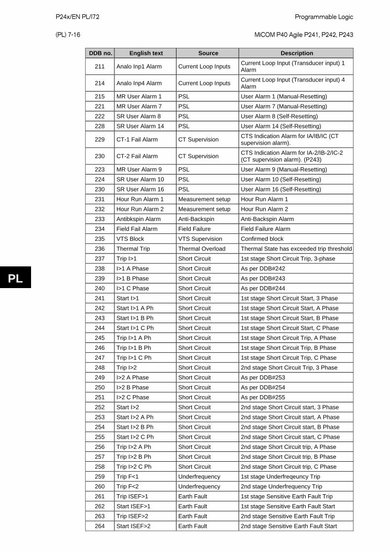
P24x/EN PL/I72
Programmable Logic (PL) 7-16 MiCOM P40 Agile P241, P242, P243
PL
DDB no. English text Source Description
211 Analo Inp1 Alarm Current Loop Inputs Current Loop Input (Transducer input) 1 Alarm
214 Analo Inp4 Alarm Current Loop Inputs Current Loop Input (Transducer input) 4 Alarm
215 MR User Alarm 1 PSL User Alarm 1 (Manual-Resetting)
221 MR User Alarm 7 PSL User Alarm 7 (Manual-Resetting)
222 SR User Alarm 8 PSL User Alarm 8 (Self-Resetting)
228 SR User Alarm 14 PSL User Alarm 14 (Self-Resetting)
229 CT-1 Fail Alarm CT Supervision CTS Indication Alarm for IA/IB/IC (CT supervision alarm).
230 CT-2 Fail Alarm CT Supervision CTS Indication Alarm for IA-2/IB-2/IC-2 (CT supervision alarm). (P243)
223 MR User Alarm 9 PSL User Alarm 9 (Manual-Resetting)
224 SR User Alarm 10 PSL User Alarm 10 (Self-Resetting)
230 SR User Alarm 16 PSL User Alarm 16 (Self-Resetting)
231 Hour Run Alarm 1 Measurement setup Hour Run Alarm 1
232 Hour Run Alarm 2 Measurement setup Hour Run Alarm 2
233 Antibkspin Alarm Anti-Backspin Anti-Backspin Alarm
234 Field Fail Alarm Field Failure Field Failure Alarm
235 VTS Block VTS Supervision Confirmed block
236 Thermal Trip Thermal Overload Thermal State has exceeded trip threshold
237 Trip I>1 Short Circuit 1st stage Short Circuit Trip, 3-phase
238 I>1 A Phase Short Circuit As per DDB#242
239 I>1 B Phase Short Circuit As per DDB#243
240 I>1 C Phase Short Circuit As per DDB#244
241 Start I>1 Short Circuit 1st stage Short Circuit Start, 3 Phase
242 Start I>1 A Ph Short Circuit 1st stage Short Circuit Start, A Phase
243 Start I>1 B Ph Short Circuit 1st stage Short Circuit Start, B Phase
244 Start I>1 C Ph Short Circuit 1st stage Short Circuit Start, C Phase
245 Trip I>1 A Ph Short Circuit 1st stage Short Circuit Trip, A Phase
246 Trip I>1 B Ph Short Circuit 1st stage Short Circuit Trip, B Phase
247 Trip I>1 C Ph Short Circuit 1st stage Short Circuit Trip, C Phase
248 Trip I>2 Short Circuit 2nd stage Short Circuit Trip, 3 Phase
249 I>2 A Phase Short Circuit As per DDB#253
250 I>2 B Phase Short Circuit As per DDB#254
251 I>2 C Phase Short Circuit As per DDB#255
252 Start I>2 Short Circuit 2nd stage Short Circuit start, 3 Phase
253 Start I>2 A Ph Short Circuit 2nd stage Short Circuit start, A Phase
254 Start I>2 B Ph Short Circuit 2nd stage Short Circuit start, B Phase
255 Start I>2 C Ph Short Circuit 2nd stage Short Circuit start, C Phase
256 Trip I>2 A Ph Short Circuit 2nd stage Short Circuit trip, A Phase
257 Trip I>2 B Ph Short Circuit 2nd stage Short Circuit trip, B Phase
258 Trip I>2 C Ph Short Circuit 2nd stage Short Circuit trip, C Phase
259 Trip F<1 Underfrequency 1st stage Underfreqeuncy Trip
260 Trip F<2 Underfrequency 2nd stage Underfrequency Trip
261 Trip ISEF>1 Earth Fault 1st stage Sensitive Earth Fault Trip
262 Start ISEF>1 Earth Fault 1st stage Sensitive Earth Fault Start
263 Trip ISEF>2 Earth Fault 2nd stage Sensitive Earth Fault Trip
264 Start ISEF>2 Earth Fault 2nd stage Sensitive Earth Fault Start
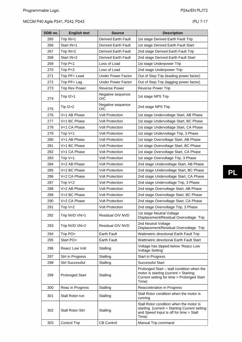
Programmable Logic
P24x/EN PL/I72 MiCOM P40 Agile P241, P242, P243 (PL) 7-17
PL
DDB no. English text Source Description 265 Trip IN>1 Derived Earth Fault 1st stage Derived Earth Fault Trip
266 Start IN>1 Derived Earth Fault 1st stage Derived Earth Fault Start
267 Trip IN>2 Derived Earth Fault 2nd stage Derived Earth Fault Trip
268 Start IN>2 Derived Earth Fault 2nd stage Derived Earth Fault Start
269 Trip P<1 Loss of Load 1st stage Underpower Trip
270 Trip P<2 Loss of Load 2nd stage Underpower Trip
271 Trip PF< Lead Under Power Factor Out of Step Trip (leading power factor)
272 Trip PF< Lag Under Power Factor Out of Step Trip (lagging power factor)
273 Trip Rev Power Reverse Power Reverse Power Trip
274 Trip I2>1 Negative sequence O/C 1st stage NPS Trip
275 Tip I2>2 Negative sequence O/C 2nd stage NPS Trip
276 V<1 AB Phase Volt Protection 1st stage Undervoltage Start, AB Phase
277 V<1 BC Phase Volt Protection 1st stage Undervoltage Start, BC Phase
278 V<1 CA Phase Volt Protection 1st stage Undervoltage Start, CA Phase
279 Trip V<1 Volt Protection 1st stage Undervoltage Trip, 3 Phase
280 V>1 AB Phase Volt Protection 1st stage Overvoltage Start, AB Phase
281 V>1 BC Phase Volt Protection 1st stage Overvoltage Start, BC Phase
282 V>1 CA Phase Volt Protection 1st stage Overvoltage Start, CA Phase
283 Trip V>1 Volt Protection 1st stage Overvoltage Trip, 3 Phase
284 V<2 AB Phase Volt Protection 2nd stage Undervoltage Start, AB Phase
285 V<2 BC Phase Volt Protection 2nd stage Undervoltage Start, BC Phase
286 V<2 CA Phase Volt Protection 2nd stage Undervoltage Start, CA Phase
287 Trip V<2 Volt Protection 2nd stage Undervoltage Trip, 3 Phase
288 V>2 AB Phase Volt Protection 2nd stage Overvoltage Start, AB Phase
289 V>2 BC Phase Volt Protection 2nd stage Overvoltage Start, BC Phase
290 V>2 CA Phase Volt Protection 2nd stage Overvoltage Start, CA Phase
291 Trip V>2 Volt Protection 2nd stage Overvoltage Trip, 3 Phase
292 Trip NVD VN>1 Residual O/V NVD 1st stage Neutral Voltage Displacement/Residual Overvoltage Trip
293 Trip NVD VN>2 Residual O/V NVD 2nd Neutral Voltage Displacement/Residual Overvoltage Trip
294 Trip PO> Earth Fault Wattmetric directional Earth Fault Trip
295 Start PO> Earth Fault Wattmetric directional Earth Fault Start
296 Reacc Low Volt Stalling Voltage has dipped below ‘Reacc Low Voltage Setting’
297 Strt in Progress Stalling Start in Progress
298 Strt Successful Stalling Successful Start
299 Prolonged Start Stalling
Prolonged Start – stall condition when the motor is starting (current > Starting Current setting for time > Prolonged Start Time)
300 Reac in Progress Stalling Reacceleration in Progress
301 Stall Rotor-run Stalling Stall Rotor condition when the motor is running
302 Stall Rotor-Strt Stalling
Stall Rotor condition when the motor is starting (current > Starting Current setting and Speed Input is off for time > Stall Time)
303 Control Trip CB Control Manual Trip command

P24x/EN PL/I72
Programmable Logic (PL) 7-18 MiCOM P40 Agile P241, P242, P243
PL
DDB no. English text Source Description 304 Control Close CB Control Manual Close command
305 Trip RTD 1 RTD Protection RTD 1 Trip
314 Trip RTD 10 RTD Protection RTD 10 Trip
315 Diff Trip A Differential Motor Differential Trip, A Phase. (P243)
316 Diff Trip B Differential Motor Differential Trip, B Phase. (P243)
317 Diff Trip C Differential Motor Differential Trip, C Phase. (P243)
318 Trip Diff Differential Motor Differential Trip (P243)
319 Trip CBF 1 CB Fail CB Fail Timer 1 Trip
320 Trip CBF 2 CB Fail CB Fail Timer 2 Trip
321 Trip Analog Inp 1 Current Loop Inputs Current Loop Input (Analog/transducer input) 1 Trip
324 Trip Analog Inp 4 Current Loop Inputs Current Loop Input (Analog/transducer input) 4 Trip
325 Pwd Ul Level 0 System Data Access Level 0 is enabled for the User Interface (HMI)
326 Pwd Ul Level 1 System Data Access Level 1 is enabled for the User Interface (HMI)
327 Pwd Ul Level 2 System Data Access Level 2 is enabled for the User Interface (HMI)
328 Pwd Front Level 0 System Data Access Level 0 is enabled for the Front Comms Port
329 Pwd Front Level 1 System Data Access Level 1 is enabled for the Front Comms Port
330 Pwd Front Level 2 System Data Access Level 2 is enabled for the Front Comms Port
331 Pwd Rear Level 0 System Data Access Level 0 is enabled for the Main Rear Comms Port
332 Pwd Rear Level 1 System Data Access Level 1 is enabled for the Main Rear Comms Port
333 Pwd Rear Level 2 System Data Access Level 2 is enabled for the Main Rear Comms Port
334 FFail1 Start Field Failure 1st Stage Field Failure Start
335 FFail2 Start Field Failure 2nd Stage Field Failure Start
336 FFail1 Trip Field Failure 1st Stage Field Failure Trip
337 FFail2 Trip Field Failure 2nd Stage Field Failure Trip
338 Trip I>3 Short Circuit 3rd stage Short Circuit Trip, 3-phase
339 I>3 A Phase Short Circuit As per DDB#343
340 I>3 B Phase Short Circuit As per DDB#344
341 I>3 C Phase Short Circuit As per DDB#345
342 Start I>3 Short Circuit 3rd stage Short Circuit Start, 3 Phase
343 Start I>3 A Ph Short Circuit 3rd stage Short Circuit Start, A Phase
344 Start I>3 B Ph Short Circuit 3rd stage Short Circuit Start, B Phase
345 Start I>3 C Ph Short Circuit 3rd stage Short Circuit Start, C Phase
346 Trip I>3 A Ph Short Circuit 3rd stage Short Circuit Trip, A Phase
347 Trip I>3 B Ph Short Circuit 3rd stage Short Circuit Trip, B Phase
348 Trip I>3 C Ph Short Circuit 3rd stage Short Circuit Trip, C Phase
349 Trip I>4 Short Circuit 4th stage Short Circuit Trip, 3-phase
350 I>4 A Phase Short Circuit As per DDB#354
351 I>4 B Phase Short Circuit As per DDB#355
352 I>4 C Phase Short Circuit As per DDB#356
353 Start I>4 Short Circuit 4th stage Short Circuit Start, 3 Phase
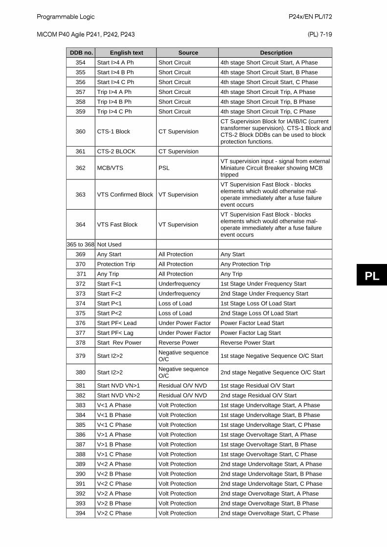
Programmable Logic
P24x/EN PL/I72 MiCOM P40 Agile P241, P242, P243 (PL) 7-19
PL
DDB no. English text Source Description 354 Start I>4 A Ph Short Circuit 4th stage Short Circuit Start, A Phase
355 Start I>4 B Ph Short Circuit 4th stage Short Circuit Start, B Phase
356 Start I>4 C Ph Short Circuit 4th stage Short Circuit Start, C Phase
357 Trip I>4 A Ph Short Circuit 4th stage Short Circuit Trip, A Phase
358 Trip I>4 B Ph Short Circuit 4th stage Short Circuit Trip, B Phase
359 Trip I>4 C Ph Short Circuit 4th stage Short Circuit Trip, C Phase
360 CTS-1 Block CT Supervision
CT Supervision Block for IA/IB/IC (current transformer supervision). CTS-1 Block and CTS-2 Block DDBs can be used to block protection functions.
361 CTS-2 BLOCK CT Supervision
362 MCB/VTS PSL VT supervision input - signal from external Miniature Circuit Breaker showing MCB tripped
363 VTS Confirmed Block VT Supervision
VT Supervision Fast Block - blocks elements which would otherwise mal-operate immediately after a fuse failure event occurs
364 VTS Fast Block VT Supervision
VT Supervision Fast Block - blocks elements which would otherwise mal-operate immediately after a fuse failure event occurs
365 to 368 Not Used
369 Any Start All Protection Any Start
370 Protection Trip All Protection Any Protection Trip
371 Any Trip All Protection Any Trip
372 Start F<1 Underfrequency 1st Stage Under Frequency Start
373 Start F<2 Underfrequency 2nd Stage Under Frequency Start
374 Start P<1 Loss of Load 1st Stage Loss Of Load Start
375 Start P<2 Loss of Load 2nd Stage Loss Of Load Start
376 Start PF< Lead Under Power Factor Power Factor Lead Start
377 Start PF< Lag Under Power Factor Power Factor Lag Start
378 Start Rev Power Reverse Power Reverse Power Start
379 Start I2>2 Negative sequence O/C 1st stage Negative Sequence O/C Start
380 Start I2>2 Negative sequence O/C 2nd stage Negative Sequence O/C Start
381 Start NVD VN>1 Residual O/V NVD 1st stage Residual O/V Start
382 Start NVD VN>2 Residual O/V NVD 2nd stage Residual O/V Start
383 V<1 A Phase Volt Protection 1st stage Undervoltage Start, A Phase
384 V<1 B Phase Volt Protection 1st stage Undervoltage Start, B Phase
385 V<1 C Phase Volt Protection 1st stage Undervoltage Start, C Phase
386 V>1 A Phase Volt Protection 1st stage Overvoltage Start, A Phase
387 V>1 B Phase Volt Protection 1st stage Overvoltage Start, B Phase
388 V>1 C Phase Volt Protection 1st stage Overvoltage Start, C Phase
389 V<2 A Phase Volt Protection 2nd stage Undervoltage Start, A Phase
390 V<2 B Phase Volt Protection 2nd stage Undervoltage Start, B Phase
391 V<2 C Phase Volt Protection 2nd stage Undervoltage Start, C Phase
392 V>2 A Phase Volt Protection 2nd stage Overvoltage Start, A Phase
393 V>2 B Phase Volt Protection 2nd stage Overvoltage Start, B Phase
394 V>2 C Phase Volt Protection 2nd stage Overvoltage Start, C Phase
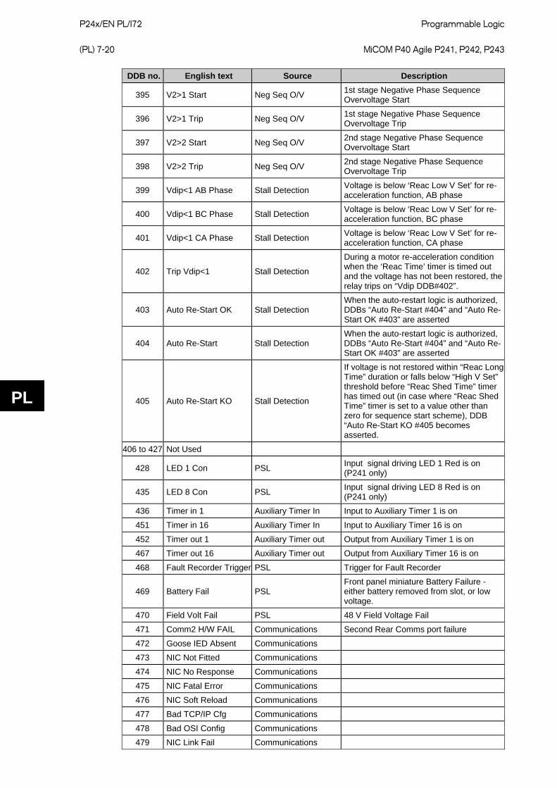
P24x/EN PL/I72
Programmable Logic (PL) 7-20 MiCOM P40 Agile P241, P242, P243
PL
DDB no. English text Source Description
395 V2>1 Start Neg Seq O/V 1st stage Negative Phase Sequence Overvoltage Start
396 V2>1 Trip Neg Seq O/V 1st stage Negative Phase Sequence Overvoltage Trip
397 V2>2 Start Neg Seq O/V 2nd stage Negative Phase Sequence Overvoltage Start
398 V2>2 Trip Neg Seq O/V 2nd stage Negative Phase Sequence Overvoltage Trip
399 Vdip<1 AB Phase Stall Detection Voltage is below ‘Reac Low V Set’ for re-acceleration function, AB phase
400 Vdip<1 BC Phase Stall Detection Voltage is below ‘Reac Low V Set’ for re-acceleration function, BC phase
401 Vdip<1 CA Phase Stall Detection Voltage is below ‘Reac Low V Set’ for re-acceleration function, CA phase
402 Trip Vdip<1 Stall Detection
During a motor re-acceleration condition when the ‘Reac Time’ timer is timed out and the voltage has not been restored, the relay trips on “Vdip DDB#402”.
403 Auto Re-Start OK Stall Detection When the auto-restart logic is authorized, DDBs “Auto Re-Start #404” and “Auto Re-Start OK #403” are asserted
404 Auto Re-Start Stall Detection When the auto-restart logic is authorized, DDBs “Auto Re-Start #404” and “Auto Re-Start OK #403” are asserted
405 Auto Re-Start KO Stall Detection
If voltage is not restored within “Reac Long Time” duration or falls below “High V Set” threshold before “Reac Shed Time” timer has timed out (in case where “Reac Shed Time” timer is set to a value other than zero for sequence start scheme), DDB “Auto Re-Start KO #405 becomes asserted.
406 to 427 Not Used
428 LED 1 Con PSL Input signal driving LED 1 Red is on (P241 only)
435 LED 8 Con PSL Input signal driving LED 8 Red is on (P241 only)
436 Timer in 1 Auxiliary Timer In Input to Auxiliary Timer 1 is on
451 Timer in 16 Auxiliary Timer In Input to Auxiliary Timer 16 is on
452 Timer out 1 Auxiliary Timer out Output from Auxiliary Timer 1 is on
467 Timer out 16 Auxiliary Timer out Output from Auxiliary Timer 16 is on
468 Fault Recorder Trigger PSL Trigger for Fault Recorder
469 Battery Fail PSL Front panel miniature Battery Failure - either battery removed from slot, or low voltage.
470 Field Volt Fail PSL 48 V Field Voltage Fail
471 Comm2 H/W FAIL Communications Second Rear Comms port failure
472 Goose IED Absent Communications
473 NIC Not Fitted Communications
474 NIC No Response Communications
475 NIC Fatal Error Communications
476 NIC Soft Reload Communications
477 Bad TCP/IP Cfg Communications
478 Bad OSI Config Communications
479 NIC Link Fail Communications
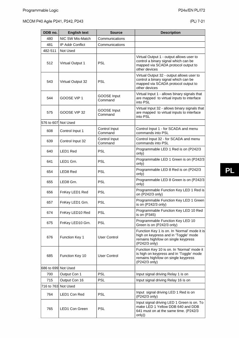
Programmable Logic
P24x/EN PL/I72 MiCOM P40 Agile P241, P242, P243 (PL) 7-21
PL
DDB no. English text Source Description 480 NIC SW Mis-Match Communications
481 IP Addr Conflict Communications
482-511 Not Used
512 Virtual Output 1 PSL
Virtual Output 1 - output allows user to control a binary signal which can be mapped via SCADA protocol output to other devices
543 Virtual Output 32 PSL
Virtual Output 32 - output allows user to control a binary signal which can be mapped via SCADA protocol output to other devices
544 GOOSE VIP 1 GOOSE Input Command
Virtual Input 1 - allows binary signals that are mapped to virtual inputs to interface into PSL
575 GOOSE VIP 32 GOOSE Input Command
Virtual Input 32 - allows binary signals that are mapped to virtual inputs to interface into PSL
576 to 607 Not Used
608 Control Input 1 Control Input Command
Control Input 1 - for SCADA and menu commands into PSL
639 Control Input 32 Control Input Command
Control Input 32 - for SCADA and menu commands into PSL
640 LED1 Red PSL Programmable LED 1 Red is on (P242/3 only)
641 LED1 Grn. PSL Programmable LED 1 Green is on (P242/3 only)
654 LED8 Red PSL Programmable LED 8 Red is on (P242/3 only)
655 LED8 Grn. PSL Programmable LED 8 Green is on (P242/3 only)
656 FnKey LED1 Red PSL Programmable Function Key LED 1 Red is on (P242/3 only)
657 FnKey LED1 Grn. PSL Programmable Function Key LED 1 Green is on (P242/3 only)
674 FnKey LED10 Red PSL Programmable Function Key LED 10 Red is on (P345)
675 FnKey LED10 Grn. PSL Programmable Function Key LED 10 Green is on (P242/3 only)
676 Function Key 1 User Control
Function Key 1 is on. In ‘Normal’ mode it is high on keypress and in ‘Toggle’ mode remains high/low on single keypress (P242/3 only)
685 Function Key 10 User Control
Function Key 10 is on. In ‘Normal’ mode it is high on keypress and in ‘Toggle’ mode remains high/low on single keypress (P242/3 only)
686 to 699 Not Used
700 Output Con 1 PSL Input signal driving Relay 1 is on
715 Output Con 16 PSL Input signal driving Relay 16 is on
716 to 763 Not Used
764 LED1 Con Red PSL Input signal driving LED 1 Red is on (P242/3 only)
765 LED1 Con Green PSL
Input signal driving LED 1 Green is on. To make LED 1 Yellow DDB 640 and DDB 641 must on at the same time. (P242/3 only))
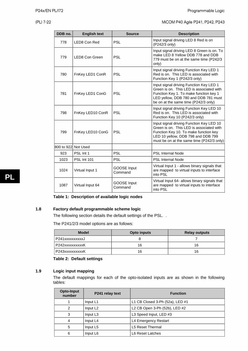
P24x/EN PL/I72
Programmable Logic (PL) 7-22 MiCOM P40 Agile P241, P242, P243
PL
DDB no. English text Source Description
778 LED8 Con Red PSL Input signal driving LED 8 Red is on (P242/3 only)
779 LED8 Con Green PSL
Input signal driving LED 8 Green is on. To make LED 8 Yellow DDB 778 and DDB 779 must be on at the same time (P242/3 only)
780 FnKey LED1 ConR PSL Input signal driving Function Key LED 1 Red is on. This LED is associated with Function Key 1 (P242/3 only)
781 FnKey LED1 ConG PSL
Input signal driving Function Key LED 1 Green is on. This LED is associated with Function Key 1. To make function key 1 LED yellow, DDB 780 and DDB 781 must be on at the same time (P242/3 only)
798 FnKey LED10 ConR PSL Input signal driving Function Key LED 10 Red is on. This LED is associated with Function Key 10 (P242/3 only)
799 FnKey LED10 ConG PSL
Input signal driving Function Key LED 10 Green is on. This LED is associated with Function Key 10. To make function key LED 10 yellow, DDB 798 and DDB 799 must be on at the same time (P242/3 only)
800 to 922 Not Used
923 PSL Int 1 PSL PSL Internal Node
1023 PSL Int 101 PSL PSL Internal Node
1024 Virtual Input 1 GOOSE Input Command
Virtual Input 1 - allows binary signals that are mapped to virtual inputs to interface into PSL
1087 Virtual Input 64 GOOSE Input Command
Virtual Input 64- allows binary signals that are mapped to virtual inputs to interface into PSL
Table 1: Description of available logic nodes
1.8 Factory default programmable scheme logic The following section details the default settings of the PSL. .
The P241/2/3 model options are as follows:
Model Opto inputs Relay outputs P241xxxxxxxxxxJ 8 7
P242xxxxxxxxxxK 16 16
P243xxxxxxxxxxK 16 16
Table 2: Default settings
1.9 Logic input mapping The default mappings for each of the opto-isolated inputs are as shown in the following tables:
Opto-Input number P241 relay text Function
1 Input L1 L1 CB Closed 3-Ph (52a), LED #1
2 Input L2 L2 CB Open 3-Ph (52b), LED #2
3 Input L3 L3 Speed Input, LED #3
4 Input L4 L4 Emergency Restart
5 Input L5 L5 Reset Thermal
6 Input L6 L6 Reset Latches
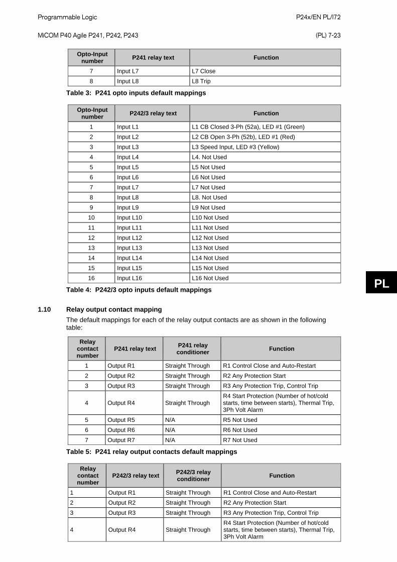
Programmable Logic
P24x/EN PL/I72 MiCOM P40 Agile P241, P242, P243 (PL) 7-23
PL
Opto-Input number P241 relay text Function
7 Input L7 L7 Close
8 Input L8 L8 Trip
Table 3: P241 opto inputs default mappings
Opto-Input number P242/3 relay text Function
1 Input L1 L1 CB Closed 3-Ph (52a), LED #1 (Green)
2 Input L2 L2 CB Open 3-Ph (52b), LED #1 (Red)
3 Input L3 L3 Speed Input, LED #3 (Yellow)
4 Input L4 L4. Not Used
5 Input L5 L5 Not Used
6 Input L6 L6 Not Used
7 Input L7 L7 Not Used
8 Input L8 L8. Not Used
9 Input L9 L9 Not Used
10 Input L10 L10 Not Used
11 Input L11 L11 Not Used
12 Input L12 L12 Not Used
13 Input L13 L13 Not Used
14 Input L14 L14 Not Used
15 Input L15 L15 Not Used
16 Input L16 L16 Not Used
Table 4: P242/3 opto inputs default mappings
1.10 Relay output contact mapping The default mappings for each of the relay output contacts are as shown in the following table:
Relay contact number
P241 relay text P241 relay conditioner Function
1 Output R1 Straight Through R1 Control Close and Auto-Restart
2 Output R2 Straight Through R2 Any Protection Start
3 Output R3 Straight Through R3 Any Protection Trip, Control Trip
4 Output R4 Straight Through R4 Start Protection (Number of hot/cold starts, time between starts), Thermal Trip, 3Ph Volt Alarm
5 Output R5 N/A R5 Not Used
6 Output R6 N/A R6 Not Used
7 Output R7 N/A R7 Not Used
Table 5: P241 relay output contacts default mappings
Relay contact number
P242/3 relay text P242/3 relay conditioner Function
1 Output R1 Straight Through R1 Control Close and Auto-Restart
2 Output R2 Straight Through R2 Any Protection Start
3 Output R3 Straight Through R3 Any Protection Trip, Control Trip
4 Output R4 Straight Through R4 Start Protection (Number of hot/cold starts, time between starts), Thermal Trip, 3Ph Volt Alarm
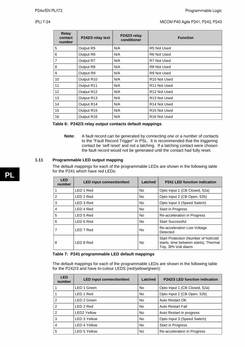
P24x/EN PL/I72
Programmable Logic (PL) 7-24 MiCOM P40 Agile P241, P242, P243
PL
Relay contact number
P242/3 relay text P242/3 relay conditioner Function
5 Output R5 N/A R5 Not Used
6 Output R6 N/A R6 Not Used
7 Output R7 N/A R7 Not Used
8 Output R8 N/A R8 Not Used
9 Output R9 N/A R9 Not Used
10 Output R10 N/A R10 Not Used
11 Output R11 N/A R11 Not Used
12 Output R12 N/A R12 Not Used
13 Output R13 N/A R13 Not Used
14 Output R14 N/A R14 Not Used
15 Output R15 N/A R15 Not Used
16 Output R16 N/A R16 Not Used
Table 6: P242/3 relay output contacts default mappings
Note: A fault record can be generated by connecting one or a number of contacts to the “Fault Record Trigger” in PSL. It is recommended that the triggering contact be ‘self reset’ and not a latching. If a latching contact were chosen the fault record would not be generated until the contact had fully reset.
1.11 Programmable LED output mapping The default mappings for each of the programmable LEDs are shown in the following table for the P241 which have red LEDs:
LED number LED input connection/text Latched P241 LED function indication
1 LED 1 Red No Opto Input 1 (CB Closed, 52a)
2 LED 2 Red No Opto Input 2 (CB Open, 52b)
3 LED 3 Red No Opto Input 3 (Speed Switch)
4 LED 4 Red No Start in Progress
5 LED 5 Red No Re-acceleration in Progress
6 LED 6 Red No Start Successful
7 LED 7 Red No Re-acceleration Low Voltage Detected
8 LED 8 Red No Start Protection (Number of hot/cold starts, time between starts), Thermal Trip, 3Ph Volt Alarm
Table 7: P241 programmable LED default mappings
The default mappings for each of the programmable LEDs are shown in the following table for the P242/3 and have tri-colour LEDS (red/yellow/green):
LED number LED input connection/text Latched P242/3 LED function indication
1 LED 1 Green No Opto Input 1 (CB Closed, 52a)
1 LED 1 Red No Opto Input 2 (CB Open, 52b)
2 LED 2 Green No Auto Restart OK
2 LED 2 Red No Auto Restart Fail
2 LED2 Yellow No Auto Restart in progress
3 LED 3 Yellow No Opto Input 3 (Speed Switch)
4 LED 4 Yellow No Start in Progress
5 LED 5 Yellow No Re-acceleration in Progress
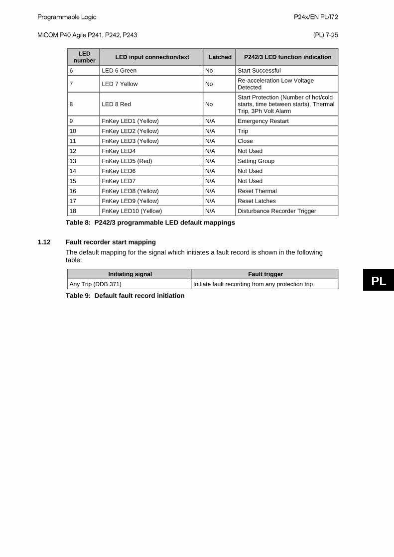
Programmable Logic
P24x/EN PL/I72 MiCOM P40 Agile P241, P242, P243 (PL) 7-25
PL
LED number LED input connection/text Latched P242/3 LED function indication
6 LED 6 Green No Start Successful
7 LED 7 Yellow No Re-acceleration Low Voltage Detected
8 LED 8 Red No Start Protection (Number of hot/cold starts, time between starts), Thermal Trip, 3Ph Volt Alarm
9 FnKey LED1 (Yellow) N/A Emergency Restart
10 FnKey LED2 (Yellow) N/A Trip
11 FnKey LED3 (Yellow) N/A Close
12 FnKey LED4 N/A Not Used
13 FnKey LED5 (Red) N/A Setting Group
14 FnKey LED6 N/A Not Used
15 FnKey LED7 N/A Not Used
16 FnKey LED8 (Yellow) N/A Reset Thermal
17 FnKey LED9 (Yellow) N/A Reset Latches
18 FnKey LED10 (Yellow) N/A Disturbance Recorder Trigger
Table 8: P242/3 programmable LED default mappings
1.12 Fault recorder start mapping The default mapping for the signal which initiates a fault record is shown in the following table:
Initiating signal Fault trigger Any Trip (DDB 371) Initiate fault recording from any protection trip
Table 9: Default fault record initiation
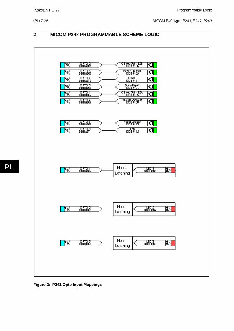
P24x/EN PL/I72
Programmable Logic (PL) 7-26 MiCOM P40 Agile P241, P242, P243
PL
2 MICOM P24x PROGRAMMABLE SCHEME LOGIC
Figure 2: P241 Opto Input Mappings
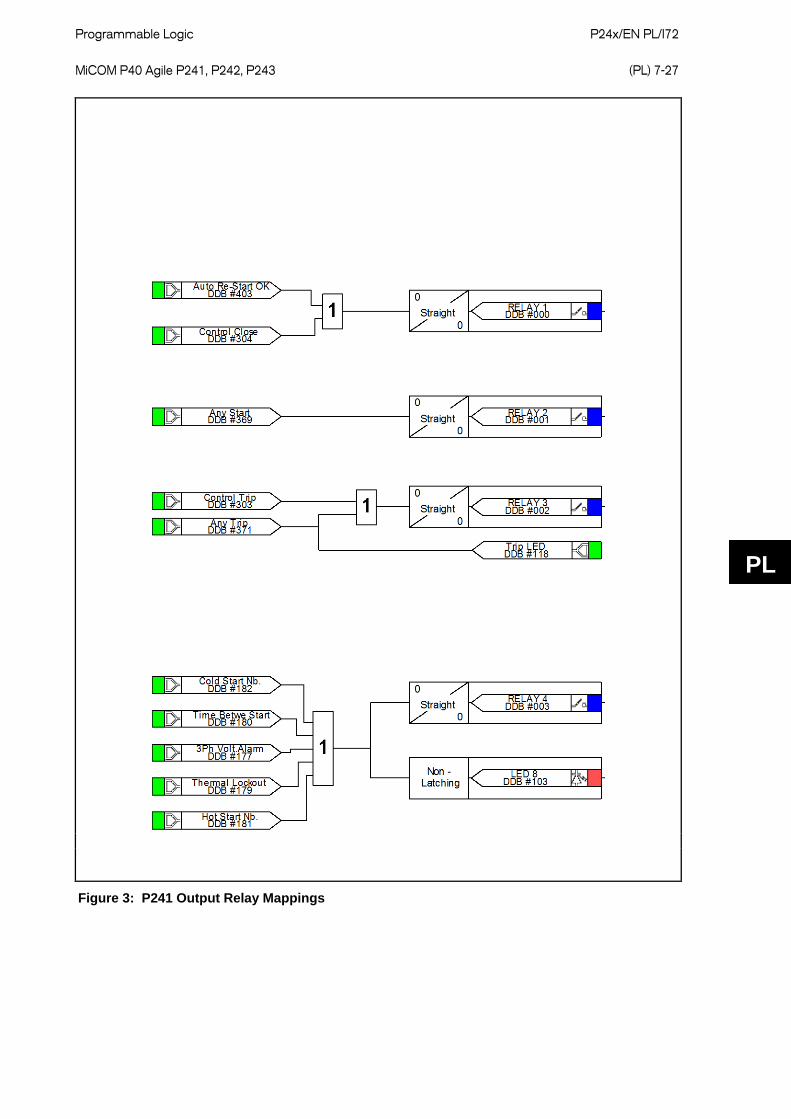
Programmable Logic
P24x/EN PL/I72 MiCOM P40 Agile P241, P242, P243 (PL) 7-27
PL
Figure 3: P241 Output Relay Mappings
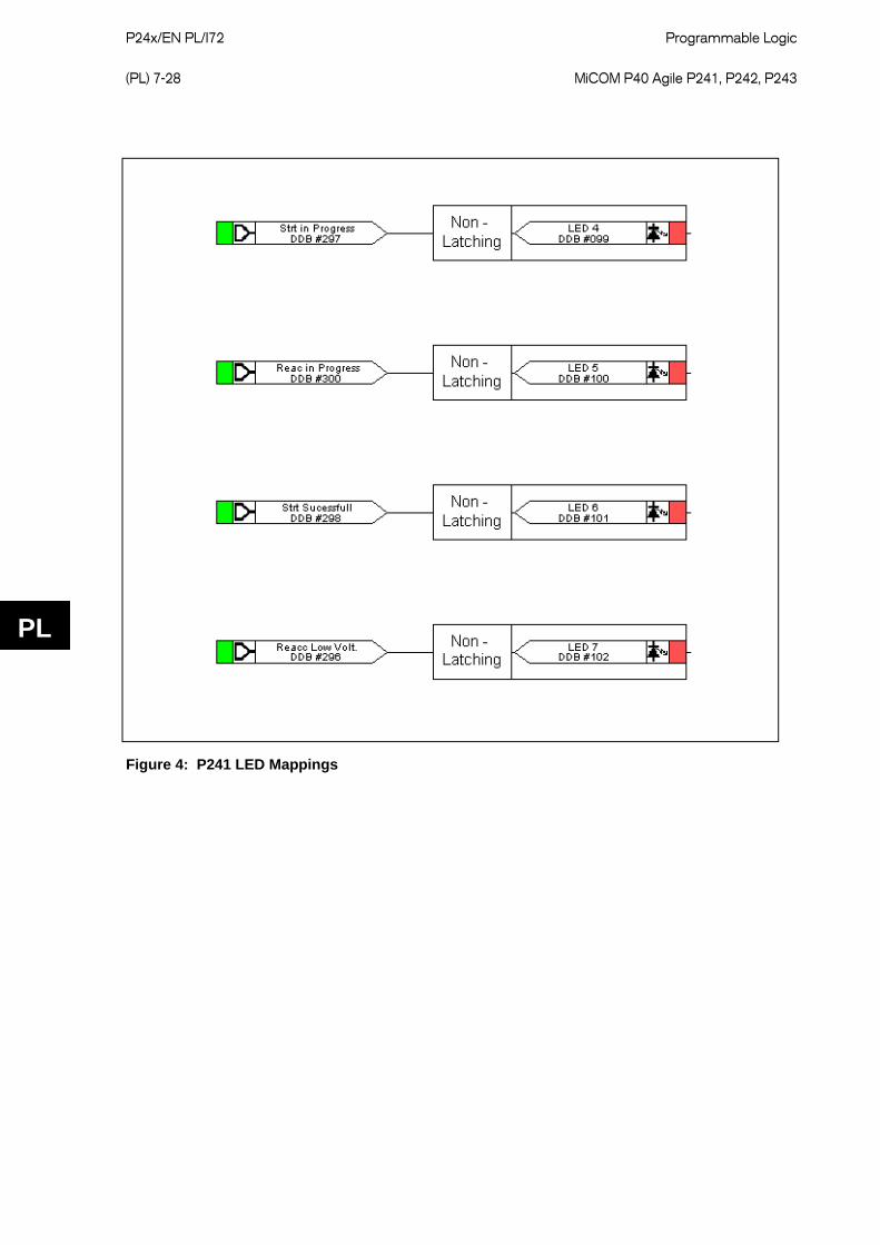
P24x/EN PL/I72
Programmable Logic (PL) 7-28 MiCOM P40 Agile P241, P242, P243
PL
Figure 4: P241 LED Mappings
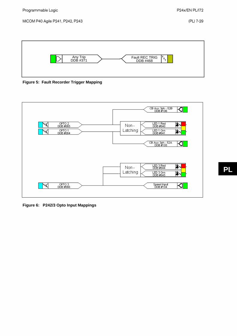
Programmable Logic
P24x/EN PL/I72 MiCOM P40 Agile P241, P242, P243 (PL) 7-29
PL
Fault REC TRIG
DDB #468Any Trip
DDB #371
Figure 5: Fault Recorder Trigger Mapping
Figure 6: P242/3 Opto Input Mappings
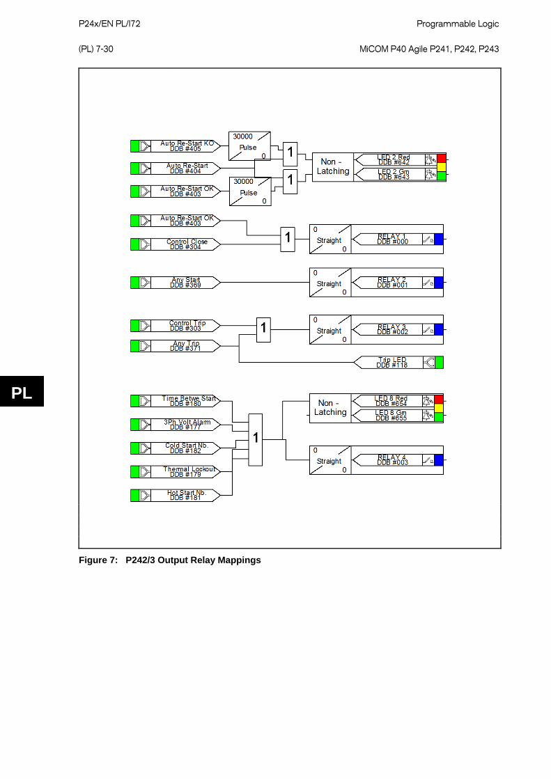
P24x/EN PL/I72
Programmable Logic (PL) 7-30 MiCOM P40 Agile P241, P242, P243
PL
Figure 7: P242/3 Output Relay Mappings
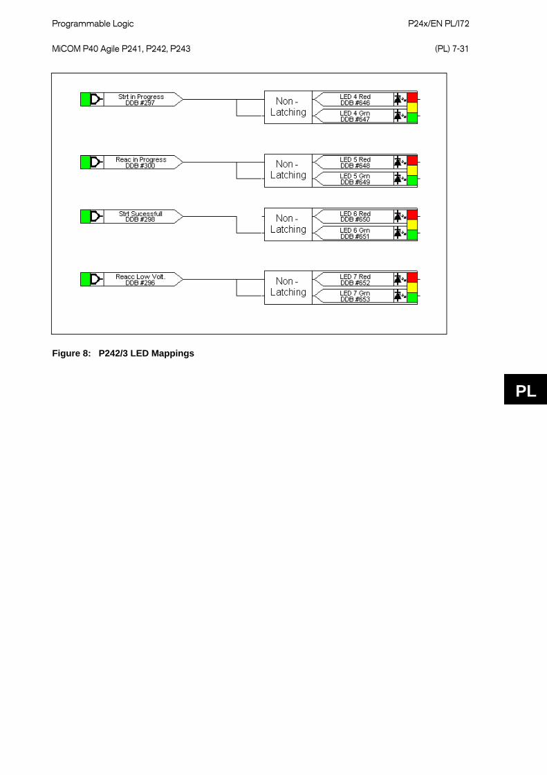
Programmable Logic
P24x/EN PL/I72 MiCOM P40 Agile P241, P242, P243 (PL) 7-31
PL
Figure 8: P242/3 LED Mappings
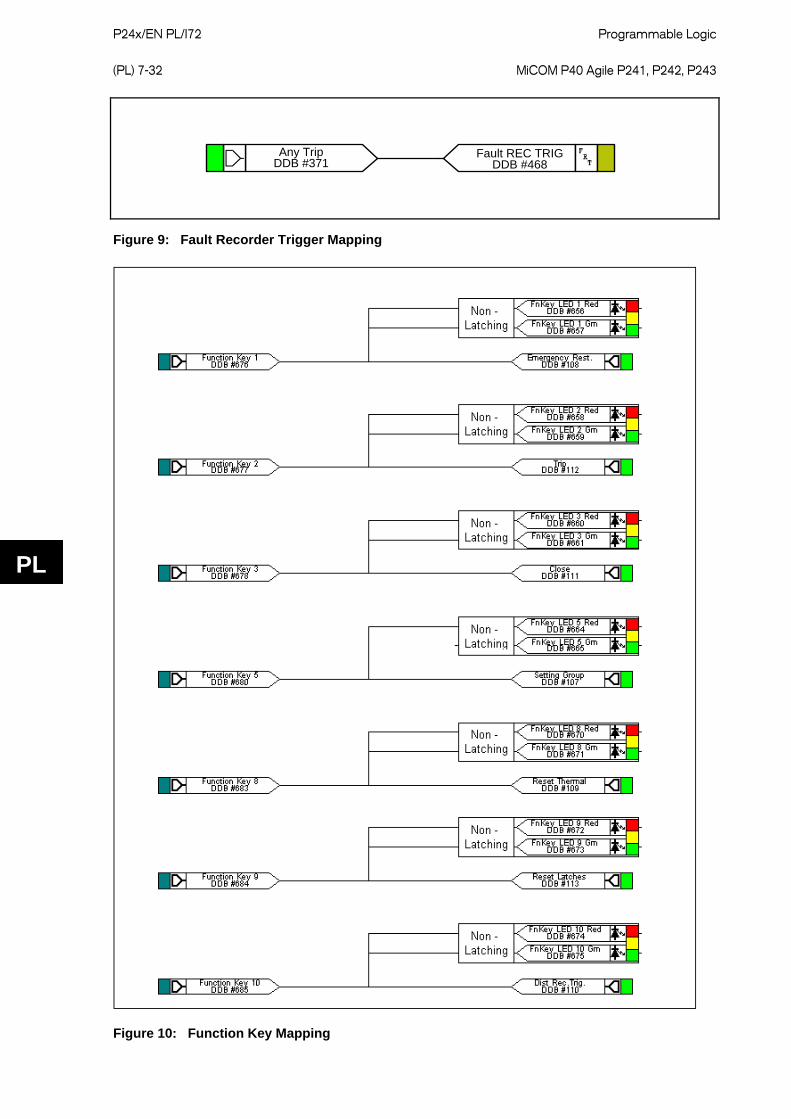
P24x/EN PL/I72
Programmable Logic (PL) 7-32 MiCOM P40 Agile P241, P242, P243
PL
Fault REC TRIG
DDB #468Any Trip
DDB #371
Figure 9: Fault Recorder Trigger Mapping
Figure 10: Function Key Mapping

Measurements and Recording
P24x/EN MR/I72 MiCOM P40 Agile P241, P242, P243 (MR) 8-1
MR MEASUREMENTS AND
RECORDING

P24x/EN MR/I72
Measurements and Recording (MR) 8-2 MiCOM P40 Agile P241, P242, P243
MR
Measurements and Recording
P24x/EN MR/I72 MiCOM P40 Agile P241, P242, P243 (MR) 8-3
MR
CONTENTS
1 MEASUREMENTS AND RECORDING 5
1.1 Introduction 5
1.2 Event & fault records 5
1.2.1 Types of event 8
1.2.1.1 Change of state of opto-isolated inputs 8
1.2.1.2 Change of state of one or more output relay contacts 8
1.2.1.3 Relay alarm conditions 8
1.2.1.4 Protection element starts and trips 10
1.2.1.5 General (platform) events 10
1.2.1.6 Fault records 10
1.2.1.7 Maintenance reports 10
1.2.1.8 Setting changes 10
1.2.2 Resetting of event/fault records 11
1.2.3 Viewing event records using MiCOM S1 Studio support software 11
1.2.4 Event filtering 12
1.3 Disturbance recorder 13
1.4 Measurements 15
1.4.1 Measured voltages and currents 15
1.4.2 Sequence voltages and currents 15
1.4.3 Power and energy quantities 15
1.4.4 Rms. voltages and currents 15
1.4.5 Demand values 15
1.4.6 Settings 16
1.4.7 Measurement display quantities 16
1.4.8 Measurements 1 17
1.4.9 Measurements 2 18
1.4.10 Measurements 3 (product specific measurements) 19
1.4.11 Measurements 4 (product specific measurements) 20
TABLES Table 1: Local viewing of records 6
Table 2: Full list of available Start and Trip elements. 8
Table 3: Examples of some of the alarm conditions and how they appear in the event list 9
Table 4: An example of a general/platform event and how it appears 10

P24x/EN MR/I72
Measurements and Recording (MR) 8-4 MiCOM P40 Agile P241, P242, P243
MR
Table 5: Examples of how setting changes are logged 11
Table 6: Filtering of event logs 13
Table 7: Disturbance Record (DR) settings 14
Table 8: Available measurement entities and corresponding settings 17
Table 9: List of Measurement 1 menu 18
Table 10: List of Measurement 2 menu 19
Table 11: List of Measurement 3 menu 20
Table 12: List of Measurement 4 menu 21
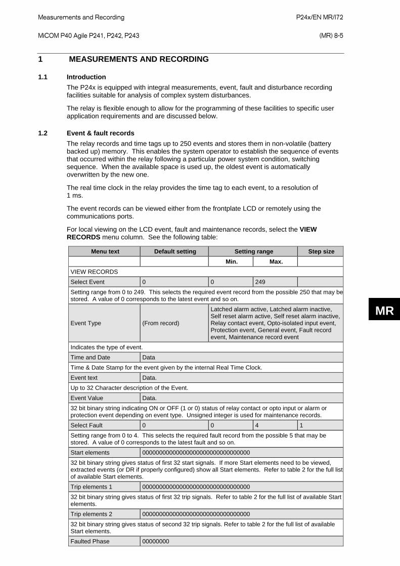
Measurements and Recording
P24x/EN MR/I72 MiCOM P40 Agile P241, P242, P243 (MR) 8-5
MR
1 MEASUREMENTS AND RECORDING
1.1 Introduction The P24x is equipped with integral measurements, event, fault and disturbance recording facilities suitable for analysis of complex system disturbances.
The relay is flexible enough to allow for the programming of these facilities to specific user application requirements and are discussed below.
1.2 Event & fault records The relay records and time tags up to 250 events and stores them in non-volatile (battery backed up) memory. This enables the system operator to establish the sequence of events that occurred within the relay following a particular power system condition, switching sequence. When the available space is used up, the oldest event is automatically overwritten by the new one.
The real time clock in the relay provides the time tag to each event, to a resolution of 1 ms.
The event records can be viewed either from the frontplate LCD or remotely using the communications ports.
For local viewing on the LCD event, fault and maintenance records, select the VIEW RECORDS menu column. See the following table:
Menu text Default setting Setting range Step size Min. Max.
VIEW RECORDS
Select Event 0 0 249
Setting range from 0 to 249. This selects the required event record from the possible 250 that may be stored. A value of 0 corresponds to the latest event and so on.
Event Type (From record)
Latched alarm active, Latched alarm inactive, Self reset alarm active, Self reset alarm inactive, Relay contact event, Opto-isolated input event, Protection event, General event, Fault record event, Maintenance record event
Indicates the type of event.
Time and Date Data
Time & Date Stamp for the event given by the internal Real Time Clock.
Event text Data.
Up to 32 Character description of the Event.
Event Value Data.
32 bit binary string indicating ON or OFF (1 or 0) status of relay contact or opto input or alarm or protection event depending on event type. Unsigned integer is used for maintenance records.
Select Fault 0 0 4 1
Setting range from 0 to 4. This selects the required fault record from the possible 5 that may be stored. A value of 0 corresponds to the latest fault and so on.
Start elements 00000000000000000000000000000000
32 bit binary string gives status of first 32 start signals. If more Start elements need to be viewed, extracted events (or DR if properly configured) show all Start elements. Refer to table 2 for the full list of available Start elements.
Trip elements 1 00000000000000000000000000000000
32 bit binary string gives status of first 32 trip signals. Refer to table 2 for the full list of available Start elements.
Trip elements 2 00000000000000000000000000000000
32 bit binary string gives status of second 32 trip signals. Refer to table 2 for the full list of available Start elements.
Faulted Phase 00000000
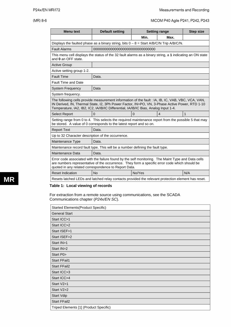
P24x/EN MR/I72
Measurements and Recording (MR) 8-6 MiCOM P40 Agile P241, P242, P243
MR
Menu text Default setting Setting range Step size Min. Max.
Displays the faulted phase as a binary string, bits 0 – 8 = Start A/B/C/N Trip A/B/C/N.
Fault Alarms 00000000000000000000000000000000
This menu cell displays the status of the 32 fault alarms as a binary string, a 1 indicating an ON state and 0 an OFF state.
Active Group
Active setting group 1-2.
Fault Time Data.
Fault Time and Date
System Frequency Data
System frequency.
The following cells provide measurement information of the fault : IA, IB, IC, VAB, VBC, VCA, VAN, IN Derived, IN, Thermal State, I2, 3Ph Power Factor, IN>PO, VN, 3-Phase Active Power, RTD 1-10 Temperature, IA2, IB2, IC2, IA/IB/IC Differential, IA/IB/IC Bias, Analog Input 1-4.
Select Report 0 0 4 1
Setting range from 0 to 4. This selects the required maintenance report from the possible 5 that may be stored. A value of 0 corresponds to the latest report and so on.
Report Text Data.
Up to 32 Character description of the occurrence.
Maintenance Type Data.
Maintenance record fault type. This will be a number defining the fault type.
Maintenance Data Data.
Error code associated with the failure found by the self monitoring. The Maint Type and Data cells are numbers representative of the occurrence. They form a specific error code which should be quoted in any related correspondence to Report Data.
Reset Indication No No/Yes N/A
Resets latched LEDs and latched relay contacts provided the relevant protection element has reset.
Table 1: Local viewing of records
For extraction from a remote source using communications, see the SCADA Communications chapter (P24x/EN SC).
Started Elements(Product Specific)
General Start
Start ICC>1
Start ICC>2
Start ISEF>1
Start ISEF>2
Start IN>1
Start IN>2
Start P0>
Start FFail1
Start FFail2
Start ICC>3
Start ICC>4
Start V2>1 Start V2>2
Start Vdip
Start FFail2
Triped Elements [1] (Product Specific)
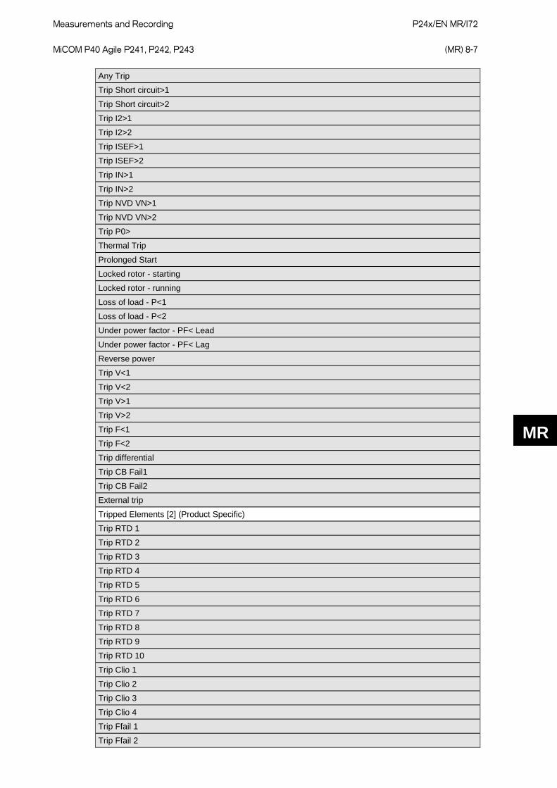
Measurements and Recording
P24x/EN MR/I72 MiCOM P40 Agile P241, P242, P243 (MR) 8-7
MR
Any Trip
Trip Short circuit>1
Trip Short circuit>2
Trip I2>1
Trip I2>2
Trip ISEF>1
Trip ISEF>2
Trip IN>1
Trip IN>2
Trip NVD VN>1
Trip NVD VN>2
Trip P0>
Thermal Trip
Prolonged Start
Locked rotor - starting
Locked rotor - running
Loss of load - P<1
Loss of load - P<2
Under power factor - PF< Lead
Under power factor - PF< Lag
Reverse power
Trip V<1
Trip V<2
Trip V>1
Trip V>2
Trip F<1
Trip F<2
Trip differential
Trip CB Fail1
Trip CB Fail2
External trip
Tripped Elements [2] (Product Specific)
Trip RTD 1
Trip RTD 2
Trip RTD 3
Trip RTD 4
Trip RTD 5
Trip RTD 6
Trip RTD 7
Trip RTD 8
Trip RTD 9
Trip RTD 10
Trip Clio 1
Trip Clio 2
Trip Clio 3
Trip Clio 4
Trip Ffail 1
Trip Ffail 2
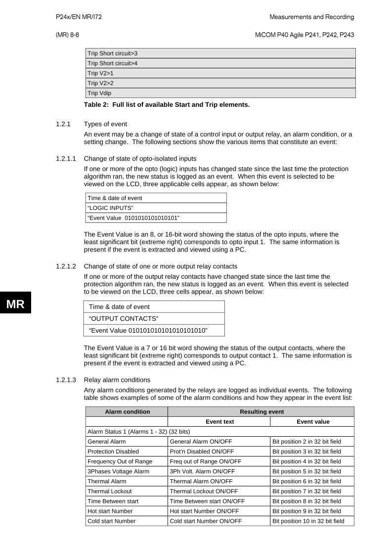
P24x/EN MR/I72
Measurements and Recording (MR) 8-8 MiCOM P40 Agile P241, P242, P243
MR
Trip Short circuit>3
Trip Short circuit>4
Trip V2>1
Trip V2>2
Trip Vdip
Table 2: Full list of available Start and Trip elements.
1.2.1 Types of event An event may be a change of state of a control input or output relay, an alarm condition, or a setting change. The following sections show the various items that constitute an event:
1.2.1.1 Change of state of opto-isolated inputs If one or more of the opto (logic) inputs has changed state since the last time the protection algorithm ran, the new status is logged as an event. When this event is selected to be viewed on the LCD, three applicable cells appear, as shown below:
Time & date of event
“LOGIC INPUTS”
“Event Value 0101010101010101” The Event Value is an 8, or 16-bit word showing the status of the opto inputs, where the least significant bit (extreme right) corresponds to opto input 1. The same information is present if the event is extracted and viewed using a PC.
1.2.1.2 Change of state of one or more output relay contacts If one or more of the output relay contacts have changed state since the last time the protection algorithm ran, the new status is logged as an event. When this event is selected to be viewed on the LCD, three cells appear, as shown below:
Time & date of event
“OUTPUT CONTACTS”
“Event Value 010101010101010101010” The Event Value is a 7 or 16 bit word showing the status of the output contacts, where the least significant bit (extreme right) corresponds to output contact 1. The same information is present if the event is extracted and viewed using a PC.
1.2.1.3 Relay alarm conditions Any alarm conditions generated by the relays are logged as individual events. The following table shows examples of some of the alarm conditions and how they appear in the event list:
Alarm condition Resulting event Event text Event value Alarm Status 1 (Alarms 1 - 32) (32 bits)
General Alarm General Alarm ON/OFF Bit position 2 in 32 bit field
Protection Disabled Prot’n Disabled ON/OFF Bit position 3 in 32 bit field
Frequency Out of Range Freq out of Range ON/OFF Bit position 4 in 32 bit field
3Phases Voltage Alarm 3Ph Volt. Alarm ON/OFF Bit position 5 in 32 bit field
Thermal Alarm Thermal Alarm ON/OFF Bit position 6 in 32 bit field
Thermal Lockout Thermal Lockout ON/OFF Bit position 7 in 32 bit field
Time Between start Time Between start ON/OFF Bit position 8 in 32 bit field
Hot start Number Hot start Number ON/OFF Bit position 9 in 32 bit field
Cold start Number Cold start Number ON/OFF Bit position 10 in 32 bit field
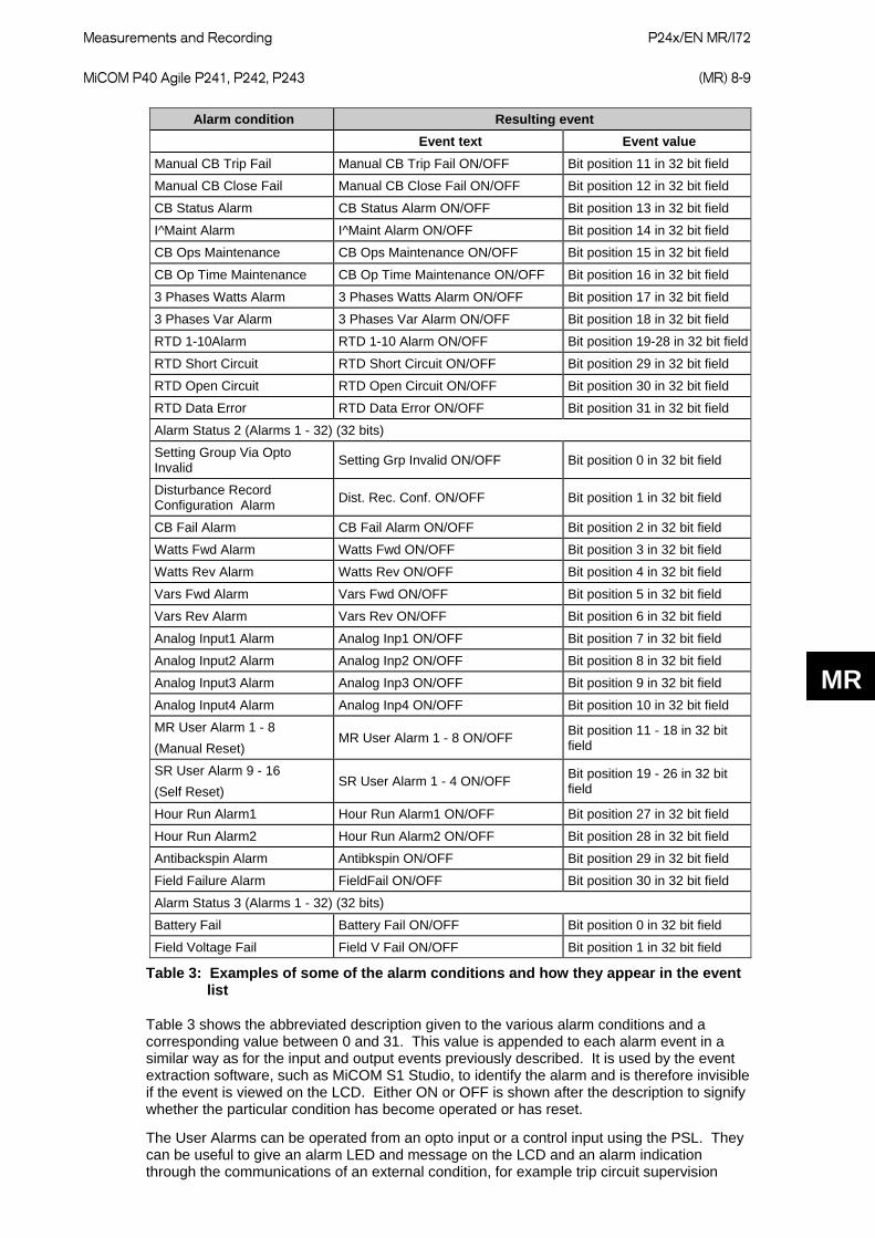
Measurements and Recording
P24x/EN MR/I72 MiCOM P40 Agile P241, P242, P243 (MR) 8-9
MR
Alarm condition Resulting event Event text Event value Manual CB Trip Fail Manual CB Trip Fail ON/OFF Bit position 11 in 32 bit field
Manual CB Close Fail Manual CB Close Fail ON/OFF Bit position 12 in 32 bit field
CB Status Alarm CB Status Alarm ON/OFF Bit position 13 in 32 bit field
I^Maint Alarm I^Maint Alarm ON/OFF Bit position 14 in 32 bit field
CB Ops Maintenance CB Ops Maintenance ON/OFF Bit position 15 in 32 bit field
CB Op Time Maintenance CB Op Time Maintenance ON/OFF Bit position 16 in 32 bit field
3 Phases Watts Alarm 3 Phases Watts Alarm ON/OFF Bit position 17 in 32 bit field
3 Phases Var Alarm 3 Phases Var Alarm ON/OFF Bit position 18 in 32 bit field
RTD 1-10Alarm RTD 1-10 Alarm ON/OFF Bit position 19-28 in 32 bit field
RTD Short Circuit RTD Short Circuit ON/OFF Bit position 29 in 32 bit field
RTD Open Circuit RTD Open Circuit ON/OFF Bit position 30 in 32 bit field
RTD Data Error RTD Data Error ON/OFF Bit position 31 in 32 bit field
Alarm Status 2 (Alarms 1 - 32) (32 bits)
Setting Group Via Opto Invalid Setting Grp Invalid ON/OFF Bit position 0 in 32 bit field
Disturbance Record Configuration Alarm Dist. Rec. Conf. ON/OFF Bit position 1 in 32 bit field
CB Fail Alarm CB Fail Alarm ON/OFF Bit position 2 in 32 bit field
Watts Fwd Alarm Watts Fwd ON/OFF Bit position 3 in 32 bit field
Watts Rev Alarm Watts Rev ON/OFF Bit position 4 in 32 bit field
Vars Fwd Alarm Vars Fwd ON/OFF Bit position 5 in 32 bit field
Vars Rev Alarm Vars Rev ON/OFF Bit position 6 in 32 bit field
Analog Input1 Alarm Analog Inp1 ON/OFF Bit position 7 in 32 bit field
Analog Input2 Alarm Analog Inp2 ON/OFF Bit position 8 in 32 bit field
Analog Input3 Alarm Analog Inp3 ON/OFF Bit position 9 in 32 bit field
Analog Input4 Alarm Analog Inp4 ON/OFF Bit position 10 in 32 bit field
MR User Alarm 1 - 8 (Manual Reset)
MR User Alarm 1 - 8 ON/OFF Bit position 11 - 18 in 32 bit field
SR User Alarm 9 - 16 (Self Reset)
SR User Alarm 1 - 4 ON/OFF Bit position 19 - 26 in 32 bit field
Hour Run Alarm1 Hour Run Alarm1 ON/OFF Bit position 27 in 32 bit field
Hour Run Alarm2 Hour Run Alarm2 ON/OFF Bit position 28 in 32 bit field
Antibackspin Alarm Antibkspin ON/OFF Bit position 29 in 32 bit field
Field Failure Alarm FieldFail ON/OFF Bit position 30 in 32 bit field
Alarm Status 3 (Alarms 1 - 32) (32 bits)
Battery Fail Battery Fail ON/OFF Bit position 0 in 32 bit field
Field Voltage Fail Field V Fail ON/OFF Bit position 1 in 32 bit field
Table 3: Examples of some of the alarm conditions and how they appear in the event list
Table 3 shows the abbreviated description given to the various alarm conditions and a corresponding value between 0 and 31. This value is appended to each alarm event in a similar way as for the input and output events previously described. It is used by the event extraction software, such as MiCOM S1 Studio, to identify the alarm and is therefore invisible if the event is viewed on the LCD. Either ON or OFF is shown after the description to signify whether the particular condition has become operated or has reset.
The User Alarms can be operated from an opto input or a control input using the PSL. They can be useful to give an alarm LED and message on the LCD and an alarm indication through the communications of an external condition, for example trip circuit supervision
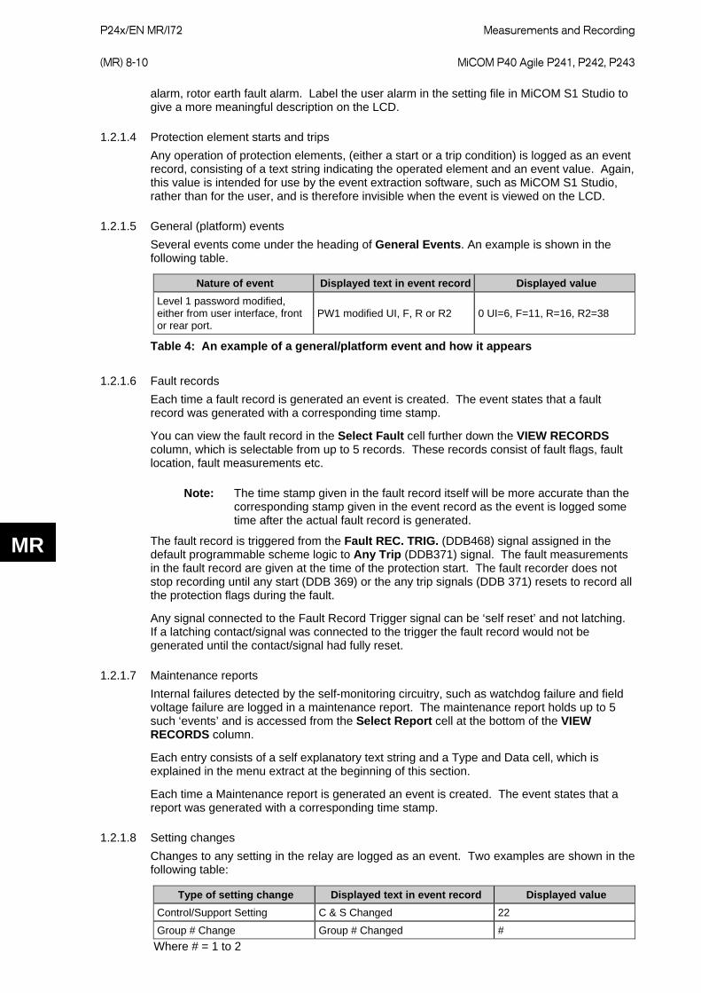
P24x/EN MR/I72
Measurements and Recording (MR) 8-10 MiCOM P40 Agile P241, P242, P243
MR
alarm, rotor earth fault alarm. Label the user alarm in the setting file in MiCOM S1 Studio to give a more meaningful description on the LCD.
1.2.1.4 Protection element starts and trips Any operation of protection elements, (either a start or a trip condition) is logged as an event record, consisting of a text string indicating the operated element and an event value. Again, this value is intended for use by the event extraction software, such as MiCOM S1 Studio, rather than for the user, and is therefore invisible when the event is viewed on the LCD.
1.2.1.5 General (platform) events Several events come under the heading of General Events. An example is shown in the following table.
Nature of event Displayed text in event record Displayed value Level 1 password modified, either from user interface, front or rear port.
PW1 modified UI, F, R or R2 0 UI=6, F=11, R=16, R2=38
Table 4: An example of a general/platform event and how it appears
1.2.1.6 Fault records Each time a fault record is generated an event is created. The event states that a fault record was generated with a corresponding time stamp.
You can view the fault record in the Select Fault cell further down the VIEW RECORDS column, which is selectable from up to 5 records. These records consist of fault flags, fault location, fault measurements etc.
Note: The time stamp given in the fault record itself will be more accurate than the corresponding stamp given in the event record as the event is logged some time after the actual fault record is generated.
The fault record is triggered from the Fault REC. TRIG. (DDB468) signal assigned in the default programmable scheme logic to Any Trip (DDB371) signal. The fault measurements in the fault record are given at the time of the protection start. The fault recorder does not stop recording until any start (DDB 369) or the any trip signals (DDB 371) resets to record all the protection flags during the fault.
Any signal connected to the Fault Record Trigger signal can be ‘self reset’ and not latching. If a latching contact/signal was connected to the trigger the fault record would not be generated until the contact/signal had fully reset.
1.2.1.7 Maintenance reports Internal failures detected by the self-monitoring circuitry, such as watchdog failure and field voltage failure are logged in a maintenance report. The maintenance report holds up to 5 such ‘events’ and is accessed from the Select Report cell at the bottom of the VIEW RECORDS column.
Each entry consists of a self explanatory text string and a Type and Data cell, which is explained in the menu extract at the beginning of this section.
Each time a Maintenance report is generated an event is created. The event states that a report was generated with a corresponding time stamp.
1.2.1.8 Setting changes Changes to any setting in the relay are logged as an event. Two examples are shown in the following table:
Type of setting change Displayed text in event record Displayed value Control/Support Setting C & S Changed 22
Group # Change Group # Changed # Where # = 1 to 2
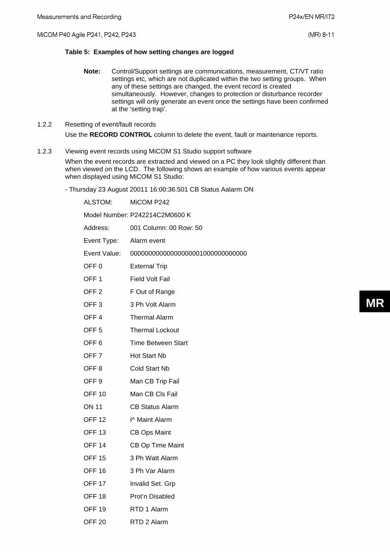
Measurements and Recording
P24x/EN MR/I72 MiCOM P40 Agile P241, P242, P243 (MR) 8-11
MR
Table 5: Examples of how setting changes are logged
Note: Control/Support settings are communications, measurement, CT/VT ratio settings etc, which are not duplicated within the two setting groups. When any of these settings are changed, the event record is created simultaneously. However, changes to protection or disturbance recorder settings will only generate an event once the settings have been confirmed at the ‘setting trap’.
1.2.2 Resetting of event/fault records Use the RECORD CONTROL column to delete the event, fault or maintenance reports.
1.2.3 Viewing event records using MiCOM S1 Studio support software When the event records are extracted and viewed on a PC they look slightly different than when viewed on the LCD. The following shows an example of how various events appear when displayed using MiCOM S1 Studio:
- Thursday 23 August 20011 16:00:36.501 CB Status Aalarm ON
ALSTOM: MiCOM P242
Model Number: P242214C2M0600 K
Address: 001 Column: 00 Row: 50
Event Type: Alarm event
Event Value: 00000000000000000001000000000000
OFF 0 External Trip
OFF 1 Field Volt Fail
OFF 2 F Out of Range
OFF 3 3 Ph Volt Alarm
OFF 4 Thermal Alarm
OFF 5 Thermal Lockout
OFF 6 Time Between Start
OFF 7 Hot Start Nb
OFF 8 Cold Start Nb
OFF 9 Man CB Trip Fail
OFF 10 Man CB Cls Fail
ON 11 CB Status Alarm
OFF 12 I^ Maint Alarm
OFF 13 CB Ops Maint
OFF 14 CB Op Time Maint
OFF 15 3 Ph Watt Alarm
OFF 16 3 Ph Var Alarm
OFF 17 Invalid Set. Grp
OFF 18 Prot’n Disabled
OFF 19 RTD 1 Alarm
OFF 20 RTD 2 Alarm
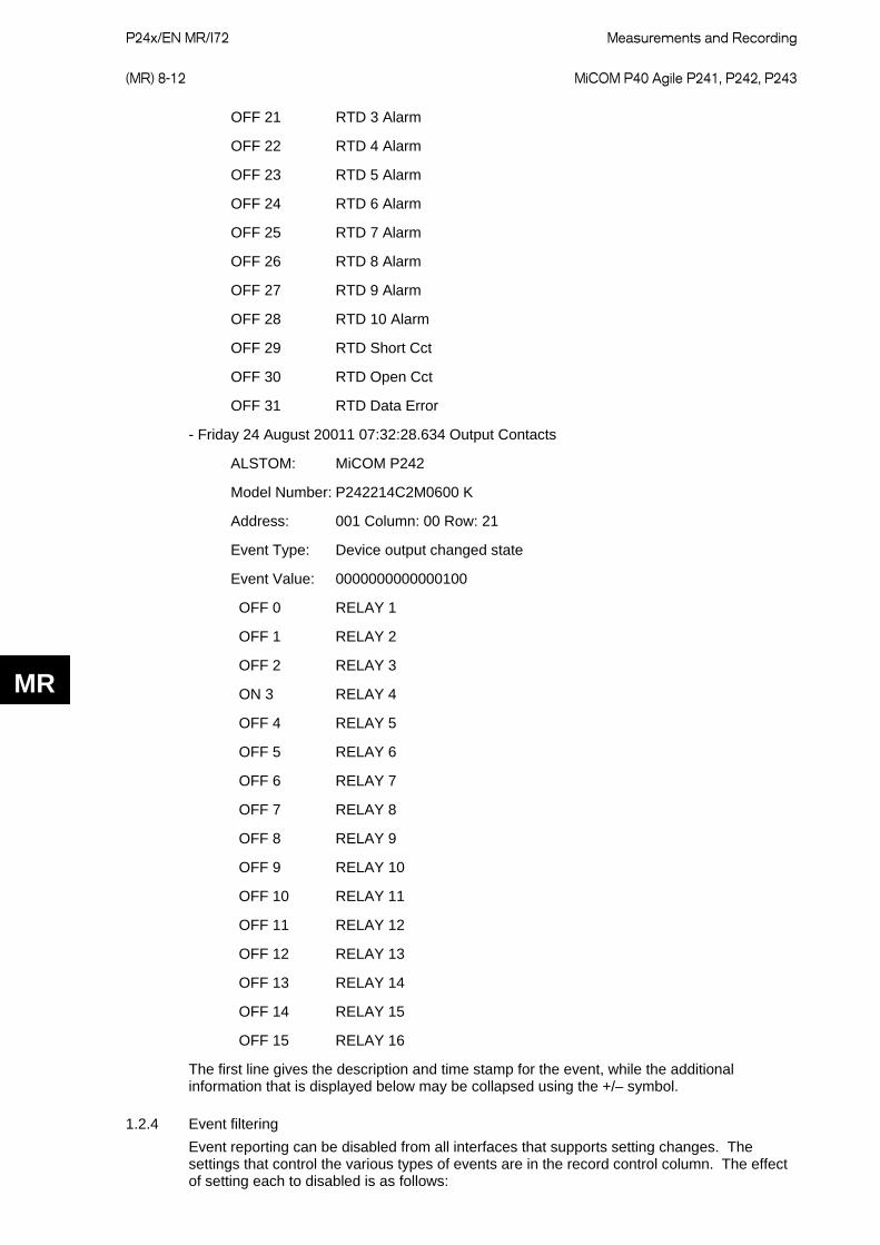
P24x/EN MR/I72
Measurements and Recording (MR) 8-12 MiCOM P40 Agile P241, P242, P243
MR
OFF 21 RTD 3 Alarm
OFF 22 RTD 4 Alarm
OFF 23 RTD 5 Alarm
OFF 24 RTD 6 Alarm
OFF 25 RTD 7 Alarm
OFF 26 RTD 8 Alarm
OFF 27 RTD 9 Alarm
OFF 28 RTD 10 Alarm
OFF 29 RTD Short Cct
OFF 30 RTD Open Cct
OFF 31 RTD Data Error
- Friday 24 August 20011 07:32:28.634 Output Contacts
ALSTOM: MiCOM P242
Model Number: P242214C2M0600 K
Address: 001 Column: 00 Row: 21
Event Type: Device output changed state
Event Value: 0000000000000100
OFF 0 RELAY 1
OFF 1 RELAY 2
OFF 2 RELAY 3
ON 3 RELAY 4
OFF 4 RELAY 5
OFF 5 RELAY 6
OFF 6 RELAY 7
OFF 7 RELAY 8
OFF 8 RELAY 9
OFF 9 RELAY 10
OFF 10 RELAY 11
OFF 11 RELAY 12
OFF 12 RELAY 13
OFF 13 RELAY 14
OFF 14 RELAY 15
OFF 15 RELAY 16
The first line gives the description and time stamp for the event, while the additional information that is displayed below may be collapsed using the +/– symbol.
1.2.4 Event filtering Event reporting can be disabled from all interfaces that supports setting changes. The settings that control the various types of events are in the record control column. The effect of setting each to disabled is as follows:

Measurements and Recording
P24x/EN MR/I72 MiCOM P40 Agile P241, P242, P243 (MR) 8-13
MR
Menu text Default setting Available settings RECORD CONTROL
Clear Events No No or Yes
Selecting Yes will cause the existing event log to be cleared and an event will be generated indicating that the events have been erased.
Clear Faults No No or Yes
Selecting Yes will cause the existing fault records to be erased from the relay.
Clear Test Log No No or Yes
Selecting Yes will cause the existing maintenance records to be erased from the relay.
Alarm Event No No/Yes
Disabling this setting means that no event will be generated for all alarms.
Output Event No No/Yes
Disabling this setting means that no event will be generated for any change in relay output contact state.
Opto Input Event No No/Yes
Disabling this setting means that no event will be generated for any change in logic input state.
Relay Sys Event No No/Yes
Disabling this setting means that no General Events will be generated.
Fault Rec Event No No/Yes
Disabling this setting means that no event will be generated for any fault that produces a fault record.
Maint. Rec Event No No/Yes
Disabling this setting means that no event will be generated for any maintenance records.
Protection Event No No/Yes
Disabling this setting means that no event will be generated for any operation of the protection elements.
DDB 31 - 0 11111111111111111111111111111111
32 bit setting to enable or disable the event recording for DDBs 0-31. For each bit 1 = event recording Enabled, 0 = event recording Disabled.
DDB 1022 - 992 11111111111111111111111111111111
32 bit setting to enable or disable the event recording for DDBs 1022 – 992. For each bit 1 = event recording Enabled, 0 = event recording Disabled. There are similar cells showing 32 bit binary strings for all DDBs from 0 – 1022. The first and last 32 bit binary strings only are shown here.
Clear Dist Recs No No/Yes
Clears all stored disturbance records from the relay
Table 6: Filtering of event logs
Note: Some occurrences will result in more than one type of event, for example a battery failure will produce an alarm event and a maintenance record event.
If the Protection Event setting is Enabled a further set of settings is revealed which allow the event generation by individual DDB signals to be enabled or disabled.
1.3 Disturbance recorder The integral disturbance recorder has an area of memory specifically set aside for record storage. The number of records that may be stored by the relay is dependent on the selected recording duration. The relay can typically store a minimum of 50 records, each of 1.5 seconds duration (8 analogue channels and 32 digital channels). However, VDEW relays have the same total record length but the VDEW protocol dictates that only 8 records can be extracted through the rear port. Disturbance records continue to record until the available memory is exhausted. The oldest record(s) are then overwritten to make space for the newest ones.
The recorder stores actual samples that are taken at a rate of 24 samples per cycle.
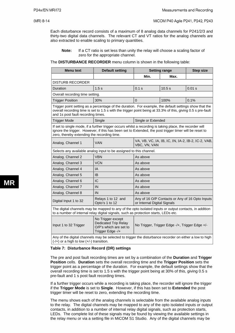
P24x/EN MR/I72
Measurements and Recording (MR) 8-14 MiCOM P40 Agile P241, P242, P243
MR
Each disturbance record consists of a maximum of 8 analog data channels for P241/2/3 and thirty-two digital data channels. The relevant CT and VT ratios for the analog channels are also extracted to enable scaling to primary quantities.
Note: If a CT ratio is set less than unity the relay will choose a scaling factor of zero for the appropriate channel.
The DISTURBANCE RECORDER menu column is shown in the following table:
Menu text Default setting Setting range Step size Min. Max.
DISTURB RECORDER
Duration 1.5 s 0.1 s 10.5 s 0.01 s
Overall recording time setting.
Trigger Position 30% 0 100% 0.1%
Trigger point setting as a percentage of the duration. For example, the default settings show that the overall recording time is set to 1.5 s with the trigger point being at 33.3% of this, giving 0.5 s pre-fault and 1s post fault recording times.
Trigger Mode Single Single or Extended
If set to single mode, if a further trigger occurs whilst a recording is taking place, the recorder will ignore the trigger. However, if this has been set to Extended, the post trigger timer will be reset to zero, thereby extending the recording time.
Analog. Channel 1 VAN VA, VB, VC, ΙA, ΙB, ΙC, ΙN, ΙA-2, ΙB-2, ΙC-2, VAB, VBC, VN, VAN
Selects any available analog input to be assigned to this channel.
Analog. Channel 2 VBN As above
Analog. Channel 3 VCN As above
Analog. Channel 4 IA As above
Analog. Channel 5 IB As above
Analog. Channel 6 IC As above
Analog. Channel 7 IN As above
Analog. Channel 8 IN As above
Digital Input 1 to 32 Relays 1 to 12 and Opto’s 1 to 12
Any of 16 O/P Contacts or Any of 16 Opto Inputs or Internal Digital Signals
The digital channels may be mapped to any of the opto isolated inputs or output contacts, in addition to a number of internal relay digital signals, such as protection starts, LEDs etc.
Input 1 to 32 Trigger
No Trigger except Dedicated Trip Relay O/P’s which are set to Trigger Edge -/+
No Trigger, Trigger Edge -/+, Trigger Edge +/-
Any of the digital channels may be selected to trigger the disturbance recorder on either a low to high (-/+) or a high to low (+/-) transition.
Table 7: Disturbance Record (DR) settings
The pre and post fault recording times are set by a combination of the Duration and Trigger Position cells. Duration sets the overall recording time and the Trigger Position sets the trigger point as a percentage of the duration. For example, the default settings show that the overall recording time is set to 1.5 s with the trigger point being at 30% of this, giving 0.5 s pre-fault and 1 s post fault recording times.
If a further trigger occurs while a recording is taking place, the recorder will ignore the trigger if the Trigger Mode is set to Single. However, if this has been set to Extended the post trigger timer will be reset to zero, extending the recording time.
The menu shows each of the analog channels is selectable from the available analog inputs to the relay. The digital channels may be mapped to any of the opto isolated inputs or output contacts, in addition to a number of internal relay digital signals, such as protection starts, LEDs. The complete list of these signals may be found by viewing the available settings in the relay menu or via a setting file in MiCOM S1 Studio. Any of the digital channels may be

Measurements and Recording
P24x/EN MR/I72 MiCOM P40 Agile P241, P242, P243 (MR) 8-15
MR
selected to trigger the disturbance recorder on either a low to high (-/+) or a high to low (+/-) transition, via the Input Trigger cell. The default trigger settings are that any dedicated trip output contacts, such as relay 3, trigger the recorder.
It is not possible to view the disturbance records locally using the LCD; they must be extracted using suitable software such as MiCOM S1 Studio. This process is fully explained in the SCADA Communications chapter, P24x/EN SC.
1.4 Measurements The relay produces a variety of both directly measured and calculated power system quantities. These measurement values are updated each second basis and can be viewed in the Measurements columns (up to four) of the relay or through MiCOM S1 Studio Measurement viewer. The P24x relay is able to measure and display the following quantities as summarized.
• Phase Voltages and Currents • Phase to Phase Voltage and Currents • Sequence Voltages and Currents • Power and Energy Quantities • Rms. Voltages and Currents • Peak and Fixed Demand Values There are also measured values from the protection functions, which are also displayed under the measurement columns of the menu; these are described in the section on the relevant protection function.
1.4.1 Measured voltages and currents The relay produces both phase-to-ground and phase-to-phase voltage and current values. They are produced directly from the DFT (Discrete Fourier Transform) used by the relay protection functions and present both magnitude and phase angle measurement.
1.4.2 Sequence voltages and currents Sequence quantities are produced by the relay from the measured Fourier values; these are displayed as magnitude values..
1.4.3 Power and energy quantities Using the measured voltages and currents the relay calculates the apparent, real and reactive power quantities. These are produced as three-phase values based on the sum of the three individual phase values. In addition to the measured power quantities the relay calculates a three-phase power factor.
These power values are also used to increment the total real and reactive energy measurements. Separate energy measurements are maintained for the total exported and imported energy. The energy measurements are incremented up to maximum values of 1000 GWhr or 1000 GVARhr at which point they will reset to zero, it is also possible to reset these values using the menu or remote interfaces using the reset demand cell.
1.4.4 Rms. voltages and currents Rms. phase voltage and current values are calculated by the relay using the sum of the samples squared over a cycle of sampled data.
1.4.5 Demand values The relay produces fixed, rolling and peak demand values. Using the reset demand menu cell it is possible to reset these quantities from the user interface or the remote communications.
Fixed demand values
The fixed demand value is the average value of a quantity over the specified interval; values are produced for each phase current and for three phase real and reactive power. The fixed

P24x/EN MR/I72
Measurements and Recording (MR) 8-16 MiCOM P40 Agile P241, P242, P243
MR
demand values displayed by the relay are those for the previous interval, the values are updated at the end of the fixed demand period.
Peak demand values
Peak demand values are produced for each phase current and the real and reactive power quantities. These display the maximum value of the measured quantity since the last reset of the demand values.
1.4.6 Settings The following settings under the heading MEASUREMENT SETUP can be used to configure the relay measurement function.
1.4.7 Measurement display quantities There are three Measurement columns available in the relay for viewing of measurement quantities. These can also be viewed with MiCOM S1 Studio (see MiCOM Px40 – Monitoring section of the MiCOM S1 Studio User Manual) and are shown below:
Menu text Default settings Available settings MEASURE’T SETUP
Default Display Description
3Ph + N Current/3Ph Voltage/Power/Date and Time/Description/Plant Reference/Frequency/Thermal State
This setting can be used to select the default display from a range of options, note that it is also possible to view the other default displays whilst at the default level using the and keys. However once the 15 minute timeout elapses the default display will revert to that selected by this setting.
Local Values Primary Primary/Secondary
This setting controls whether measured values via the front panel user interface and the front courier port are displayed as primary or secondary quantities.
Remote Values Primary Primary/Secondary
This setting controls whether measured values via the rear communication port are displayed as primary or secondary quantities.
Measurement Ref. VA VA/VB/VC/ΙA/ΙB/ΙC
Using this setting the phase reference for all angular measurements by the relay can be selected.
Fix Dem Period 30 minutes 1 to 99 minutes step 1 minute
This setting defines the length of the fixed demand window.
Alarm Fix Dem Invisible Invisible/Visible
Sets the Alarm Fix Demand Status menu visible in the relay settings.
3Ph W Thresh 50 Vn*In 1 Vn*In 120 Vn*In
3 phase watt alarm setting.
3Ph VArs Thresh 50 Vn*In 1 Vn*In 120 Vn*In
3 phase VArs alarm setting.
Alarm Energies Invisible Invisible/Visible
Sets the Alarm Energies Status menu visible in the relay settings.
W Fwd Thresh 50 V1*I1 1 Vn*In 1000 Vn*In
3 phase Watt Hour Forward alarm setting.
W Rev Thresh 50 V1*I1 1 Vn*In 1000 Vn*In
3 phase Watt Hour Reverse alarm setting.
VAr Fwd Thresh 50 V1*I1 1 Vn*In 1000 Vn*In
3 phase VAr Hour Forward alarm setting.
VAr Rev Thresh 50 V1*I1 1 Vn*In 1000 Vn*In
3 phase VAr Hour Reverse alarm setting.
Motor Hour Run > 1 Disabled Disabled/Enabled
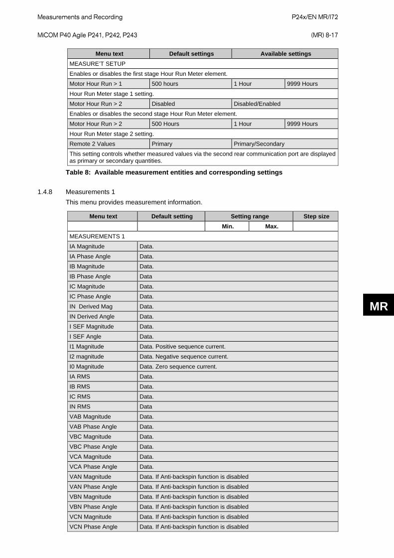
Measurements and Recording
P24x/EN MR/I72 MiCOM P40 Agile P241, P242, P243 (MR) 8-17
MR
Menu text Default settings Available settings MEASURE’T SETUP
Enables or disables the first stage Hour Run Meter element.
Motor Hour Run > 1 500 hours 1 Hour 9999 Hours
Hour Run Meter stage 1 setting.
Motor Hour Run > 2 Disabled Disabled/Enabled
Enables or disables the second stage Hour Run Meter element.
Motor Hour Run > 2 500 Hours 1 Hour 9999 Hours
Hour Run Meter stage 2 setting.
Remote 2 Values Primary Primary/Secondary
This setting controls whether measured values via the second rear communication port are displayed as primary or secondary quantities.
Table 8: Available measurement entities and corresponding settings
1.4.8 Measurements 1 This menu provides measurement information.
Menu text Default setting Setting range Step size Min. Max.
MEASUREMENTS 1
IA Magnitude Data.
IA Phase Angle Data.
IB Magnitude Data.
IB Phase Angle Data
IC Magnitude Data.
IC Phase Angle Data.
IN Derived Mag Data.
IN Derived Angle Data.
I SEF Magnitude Data.
I SEF Angle Data.
I1 Magnitude Data. Positive sequence current.
I2 magnitude Data. Negative sequence current.
I0 Magnitude Data. Zero sequence current.
IA RMS Data.
IB RMS Data.
IC RMS Data.
IN RMS Data
VAB Magnitude Data.
VAB Phase Angle Data.
VBC Magnitude Data.
VBC Phase Angle Data.
VCA Magnitude Data.
VCA Phase Angle Data.
VAN Magnitude Data. If Anti-backspin function is disabled
VAN Phase Angle Data. If Anti-backspin function is disabled
VBN Magnitude Data. If Anti-backspin function is disabled
VBN Phase Angle Data. If Anti-backspin function is disabled
VCN Magnitude Data. If Anti-backspin function is disabled
VCN Phase Angle Data. If Anti-backspin function is disabled
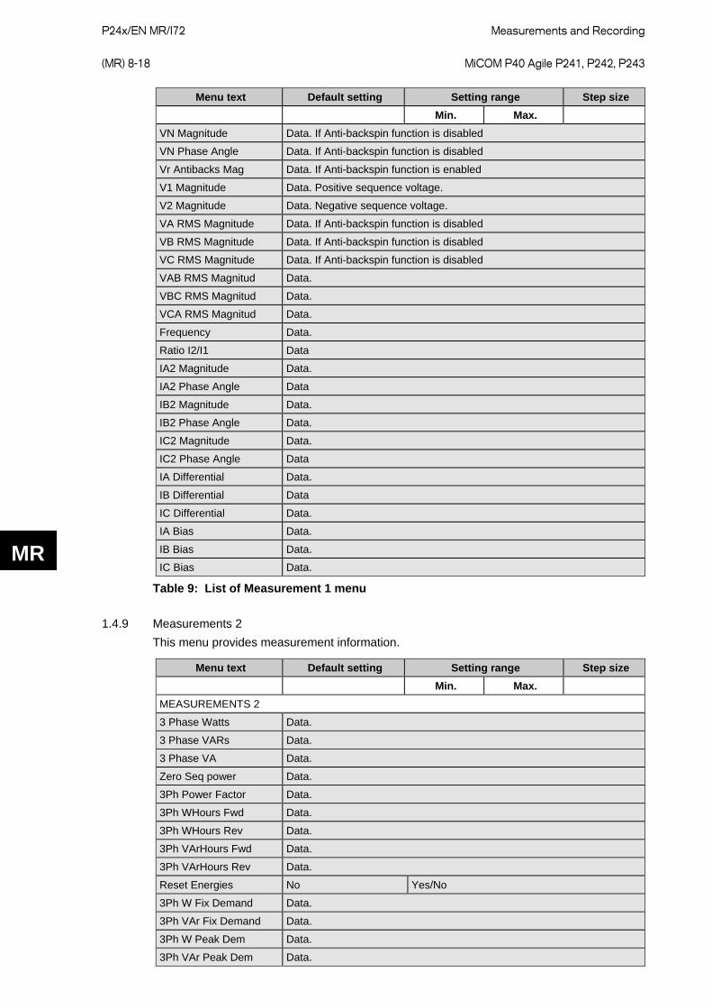
P24x/EN MR/I72
Measurements and Recording (MR) 8-18 MiCOM P40 Agile P241, P242, P243
MR
Menu text Default setting Setting range Step size Min. Max.
VN Magnitude Data. If Anti-backspin function is disabled
VN Phase Angle Data. If Anti-backspin function is disabled
Vr Antibacks Mag Data. If Anti-backspin function is enabled
V1 Magnitude Data. Positive sequence voltage.
V2 Magnitude Data. Negative sequence voltage.
VA RMS Magnitude Data. If Anti-backspin function is disabled
VB RMS Magnitude Data. If Anti-backspin function is disabled
VC RMS Magnitude Data. If Anti-backspin function is disabled
VAB RMS Magnitud Data.
VBC RMS Magnitud Data.
VCA RMS Magnitud Data.
Frequency Data.
Ratio I2/I1 Data
IA2 Magnitude Data.
IA2 Phase Angle Data
IB2 Magnitude Data.
IB2 Phase Angle Data.
IC2 Magnitude Data.
IC2 Phase Angle Data
IA Differential Data.
IB Differential Data
IC Differential Data.
IA Bias Data.
IB Bias Data.
IC Bias Data.
Table 9: List of Measurement 1 menu
1.4.9 Measurements 2 This menu provides measurement information.
Menu text Default setting Setting range Step size Min. Max.
MEASUREMENTS 2
3 Phase Watts Data.
3 Phase VARs Data.
3 Phase VA Data.
Zero Seq power Data.
3Ph Power Factor Data.
3Ph WHours Fwd Data.
3Ph WHours Rev Data.
3Ph VArHours Fwd Data.
3Ph VArHours Rev Data.
Reset Energies No Yes/No
3Ph W Fix Demand Data.
3Ph VAr Fix Demand Data.
3Ph W Peak Dem Data.
3Ph VAr Peak Dem Data.
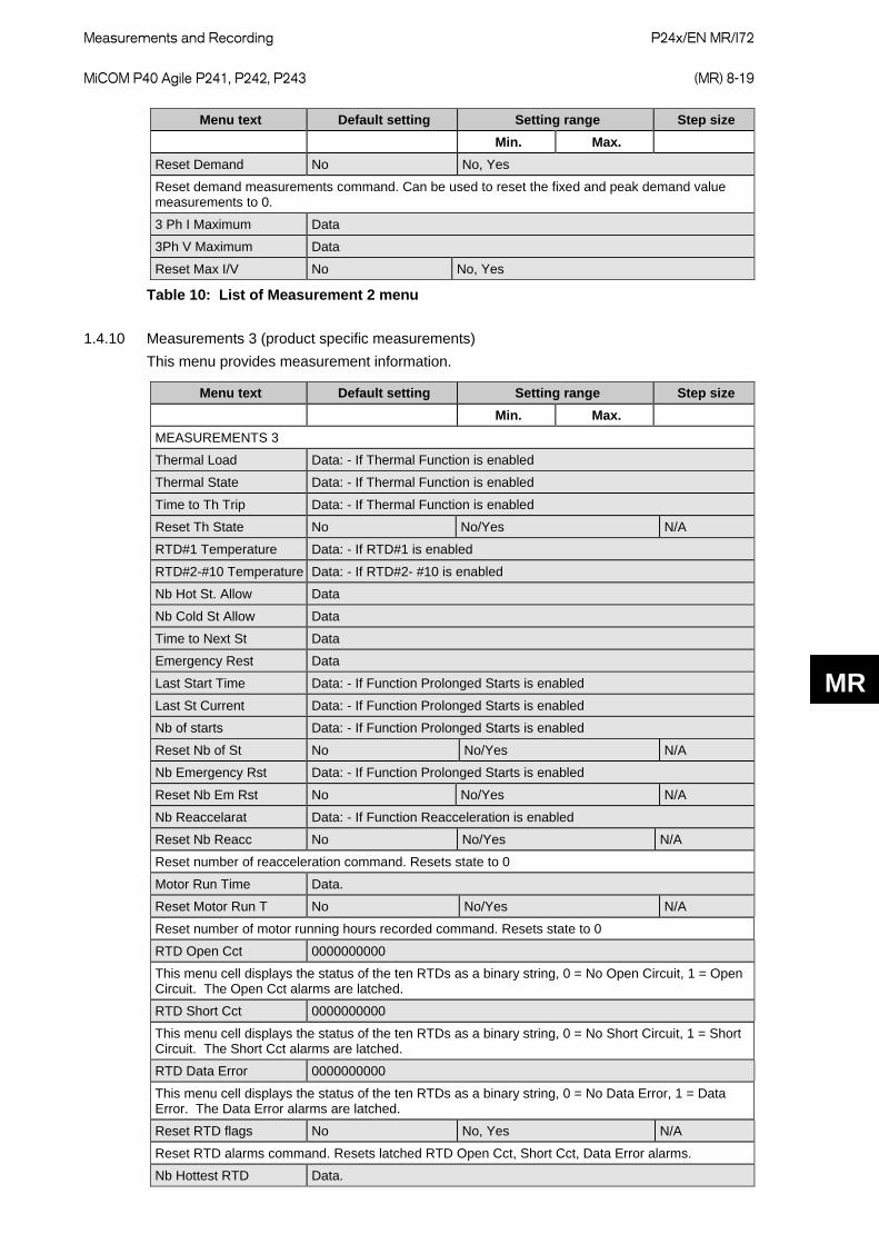
Measurements and Recording
P24x/EN MR/I72 MiCOM P40 Agile P241, P242, P243 (MR) 8-19
MR
Menu text Default setting Setting range Step size Min. Max.
Reset Demand No No, Yes
Reset demand measurements command. Can be used to reset the fixed and peak demand value measurements to 0.
3 Ph I Maximum Data
3Ph V Maximum Data
Reset Max I/V No No, Yes
Table 10: List of Measurement 2 menu
1.4.10 Measurements 3 (product specific measurements) This menu provides measurement information.
Menu text Default setting Setting range Step size Min. Max.
MEASUREMENTS 3
Thermal Load Data: - If Thermal Function is enabled
Thermal State Data: - If Thermal Function is enabled
Time to Th Trip Data: - If Thermal Function is enabled
Reset Th State No No/Yes N/A
RTD#1 Temperature Data: - If RTD#1 is enabled
RTD#2-#10 Temperature Data: - If RTD#2- #10 is enabled
Nb Hot St. Allow Data
Nb Cold St Allow Data
Time to Next St Data
Emergency Rest Data
Last Start Time Data: - If Function Prolonged Starts is enabled
Last St Current Data: - If Function Prolonged Starts is enabled
Nb of starts Data: - If Function Prolonged Starts is enabled
Reset Nb of St No No/Yes N/A
Nb Emergency Rst Data: - If Function Prolonged Starts is enabled
Reset Nb Em Rst No No/Yes N/A
Nb Reaccelarat Data: - If Function Reacceleration is enabled
Reset Nb Reacc No No/Yes N/A
Reset number of reacceleration command. Resets state to 0
Motor Run Time Data.
Reset Motor Run T No No/Yes N/A
Reset number of motor running hours recorded command. Resets state to 0
RTD Open Cct 0000000000
This menu cell displays the status of the ten RTDs as a binary string, 0 = No Open Circuit, 1 = Open Circuit. The Open Cct alarms are latched.
RTD Short Cct 0000000000
This menu cell displays the status of the ten RTDs as a binary string, 0 = No Short Circuit, 1 = Short Circuit. The Short Cct alarms are latched.
RTD Data Error 0000000000
This menu cell displays the status of the ten RTDs as a binary string, 0 = No Data Error, 1 = Data Error. The Data Error alarms are latched.
Reset RTD flags No No, Yes N/A
Reset RTD alarms command. Resets latched RTD Open Cct, Short Cct, Data Error alarms.
Nb Hottest RTD Data.
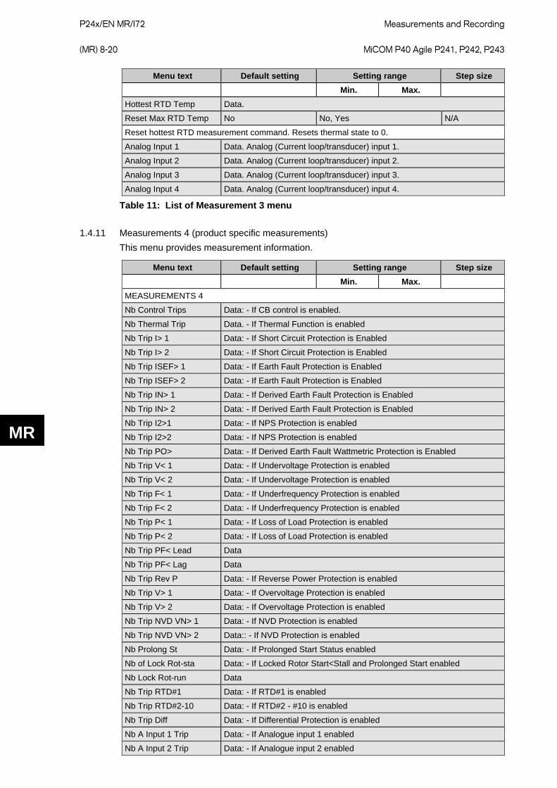
P24x/EN MR/I72
Measurements and Recording (MR) 8-20 MiCOM P40 Agile P241, P242, P243
MR
Menu text Default setting Setting range Step size Min. Max.
Hottest RTD Temp Data.
Reset Max RTD Temp No No, Yes N/A
Reset hottest RTD measurement command. Resets thermal state to 0.
Analog Input 1 Data. Analog (Current loop/transducer) input 1.
Analog Input 2 Data. Analog (Current loop/transducer) input 2.
Analog Input 3 Data. Analog (Current loop/transducer) input 3.
Analog Input 4 Data. Analog (Current loop/transducer) input 4.
Table 11: List of Measurement 3 menu
1.4.11 Measurements 4 (product specific measurements) This menu provides measurement information.
Menu text Default setting Setting range Step size Min. Max.
MEASUREMENTS 4
Nb Control Trips Data: - If CB control is enabled.
Nb Thermal Trip Data. - If Thermal Function is enabled
Nb Trip I> 1 Data: - If Short Circuit Protection is Enabled
Nb Trip I> 2 Data: - If Short Circuit Protection is Enabled
Nb Trip ISEF> 1 Data: - If Earth Fault Protection is Enabled
Nb Trip ISEF> 2 Data: - If Earth Fault Protection is Enabled
Nb Trip IN> 1 Data: - If Derived Earth Fault Protection is Enabled
Nb Trip IN> 2 Data: - If Derived Earth Fault Protection is Enabled
Nb Trip I2>1 Data: - If NPS Protection is enabled
Nb Trip I2>2 Data: - If NPS Protection is enabled
Nb Trip PO> Data: - If Derived Earth Fault Wattmetric Protection is Enabled
Nb Trip V< 1 Data: - If Undervoltage Protection is enabled
Nb Trip V< 2 Data: - If Undervoltage Protection is enabled
Nb Trip F< 1 Data: - If Underfrequency Protection is enabled
Nb Trip F< 2 Data: - If Underfrequency Protection is enabled
Nb Trip P< 1 Data: - If Loss of Load Protection is enabled
Nb Trip P< 2 Data: - If Loss of Load Protection is enabled
Nb Trip PF< Lead Data
Nb Trip PF< Lag Data
Nb Trip Rev P Data: - If Reverse Power Protection is enabled
Nb Trip V> 1 Data: - If Overvoltage Protection is enabled
Nb Trip V> 2 Data: - If Overvoltage Protection is enabled
Nb Trip NVD VN> 1 Data: - If NVD Protection is enabled
Nb Trip NVD VN> 2 Data:: - If NVD Protection is enabled
Nb Prolong St Data: - If Prolonged Start Status enabled
Nb of Lock Rot-sta Data: - If Locked Rotor Start<Stall and Prolonged Start enabled
Nb Lock Rot-run Data
Nb Trip RTD#1 Data: - If RTD#1 is enabled
Nb Trip RTD#2-10 Data: - If RTD#2 - #10 is enabled
Nb Trip Diff Data: - If Differential Protection is enabled
Nb A Input 1 Trip Data: - If Analogue input 1 enabled
Nb A Input 2 Trip Data: - If Analogue input 2 enabled
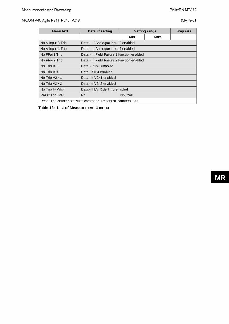
Measurements and Recording
P24x/EN MR/I72 MiCOM P40 Agile P241, P242, P243 (MR) 8-21
MR
Menu text Default setting Setting range Step size Min. Max.
Nb A Input 3 Trip Data: - If Analogue input 3 enabled
Nb A Input 4 Trip Data: - If Analogue input 4 enabled
Nb FFail1 Trip Data - If Field Failure 1 function enabled
Nb FFail2 Trip Data - If Field Failure 2 function enabled
Nb Trip I> 3 Data - if I>3 enabled
Nb Trip I> 4 Data - if I>4 enabled
Nb Trip V2> 1 Data - if V2>1 enabled
Nb Trip V2> 2 Data - if V2>2 enabled
Nb Trip I> Vdip Data - if LV Ride Thru enabled
Reset Trip Stat No No, Yes
Reset Trip counter statistics command. Resets all counters to 0
Table 12: List of Measurement 4 menu

P24x/EN MR/I72
Measurements and Recording (MR) 8-22 MiCOM P40 Agile P241, P242, P243
MR

Firmware Design
P24x/EN FD/I72 MiCOM P40 Agile P241, P242, P243 (FD) 9-1
FD
FIRMWARE DESIGN

P24x/EN FD/I72
Firmware Design (FD) 9-2 MiCOM P40 Agile P241, P242, P243
FD
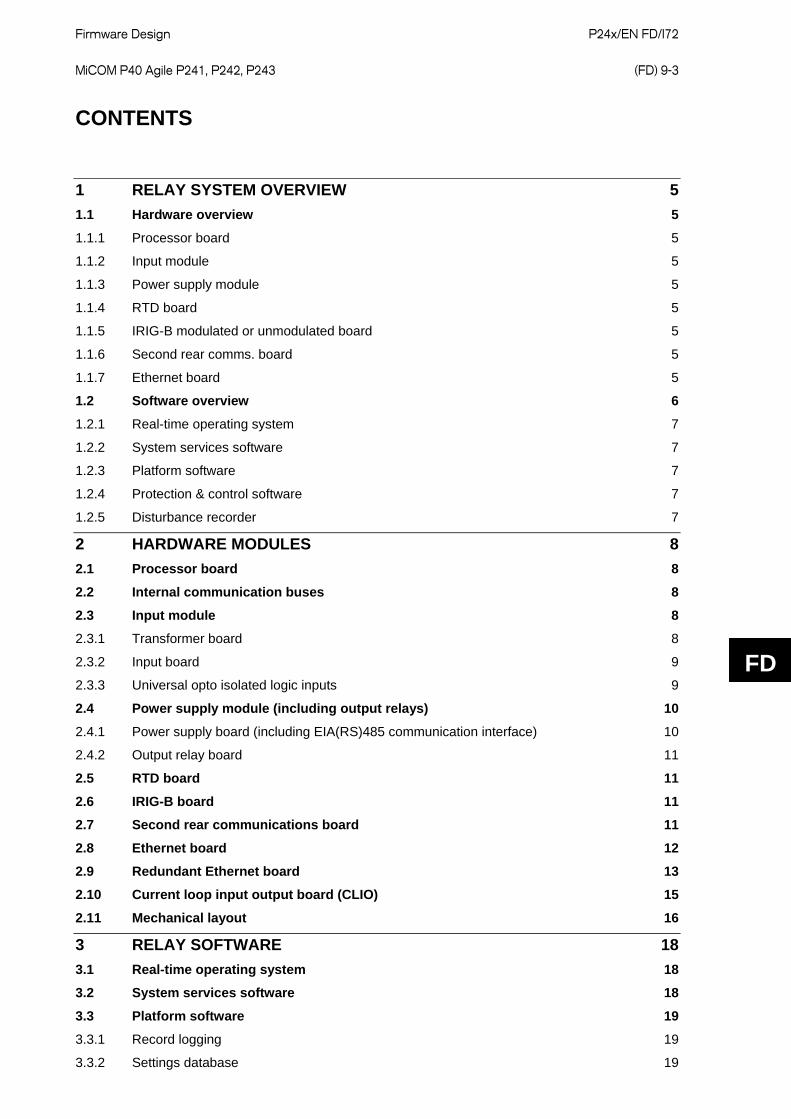
Firmware Design
P24x/EN FD/I72 MiCOM P40 Agile P241, P242, P243 (FD) 9-3
FD
CONTENTS
1 RELAY SYSTEM OVERVIEW 5
1.1 Hardware overview 5
1.1.1 Processor board 5
1.1.2 Input module 5
1.1.3 Power supply module 5
1.1.4 RTD board 5
1.1.5 IRIG-B modulated or unmodulated board 5
1.1.6 Second rear comms. board 5
1.1.7 Ethernet board 5
1.2 Software overview 6
1.2.1 Real-time operating system 7
1.2.2 System services software 7
1.2.3 Platform software 7
1.2.4 Protection & control software 7
1.2.5 Disturbance recorder 7
2 HARDWARE MODULES 8
2.1 Processor board 8
2.2 Internal communication buses 8
2.3 Input module 8
2.3.1 Transformer board 8
2.3.2 Input board 9
2.3.3 Universal opto isolated logic inputs 9
2.4 Power supply module (including output relays) 10
2.4.1 Power supply board (including EIA(RS)485 communication interface) 10
2.4.2 Output relay board 11
2.5 RTD board 11
2.6 IRIG-B board 11
2.7 Second rear communications board 11
2.8 Ethernet board 12
2.9 Redundant Ethernet board 13
2.10 Current loop input output board (CLIO) 15
2.11 Mechanical layout 16
3 RELAY SOFTWARE 18
3.1 Real-time operating system 18
3.2 System services software 18
3.3 Platform software 19
3.3.1 Record logging 19
3.3.2 Settings database 19
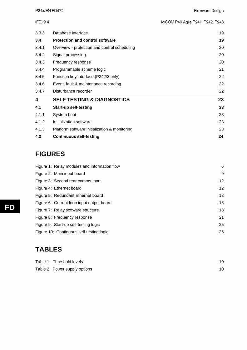
P24x/EN FD/I72
Firmware Design (FD) 9-4 MiCOM P40 Agile P241, P242, P243
FD
3.3.3 Database interface 19
3.4 Protection and control software 19
3.4.1 Overview - protection and control scheduling 20
3.4.2 Signal processing 20
3.4.3 Frequency response 20
3.4.4 Programmable scheme logic 21
3.4.5 Function key interface (P242/3 only) 22
3.4.6 Event, fault & maintenance recording 22
3.4.7 Disturbance recorder 22
4 SELF TESTING & DIAGNOSTICS 23
4.1 Start-up self-testing 23
4.1.1 System boot 23
4.1.2 Initialization software 23
4.1.3 Platform software initialization & monitoring 23
4.2 Continuous self-testing 24
FIGURES Figure 1: Relay modules and information flow 6
Figure 2: Main input board 9
Figure 3: Second rear comms. port 12
Figure 4: Ethernet board 12
Figure 5: Redundant Ethernet board 13
Figure 6: Current loop input output board 16
Figure 7: Relay software structure 18
Figure 8: Frequency response 21
Figure 9: Start-up self-testing logic 25
Figure 10: Continuous self-testing logic 26
TABLES Table 1: Threshold levels 10
Table 2: Power supply options 10

Firmware Design
P24x/EN FD/I72 MiCOM P40 Agile P241, P242, P243 (FD) 9-5
FD
1 RELAY SYSTEM OVERVIEW
1.1 Hardware overview The relay hardware is made up of several modules from a standard range. Some modules are essential while others are optional depending on the user’s requirements.
The different modules that can be present in the relay are as follows:
1.1.1 Processor board The processor board performs all calculations for the relay and controls the operation of all other modules within the relay. The processor board also contains and controls the user interfaces (LCD, LEDs, keypad and communication interfaces).
1.1.2 Input module The input module converts the data in the analog and digital input signals into a format suitable for processing by the processor board. The standard input module consists of two boards; a transformer board to provide electrical isolation and a main input board which provides analog to digital conversion and the isolated digital inputs.
1.1.3 Power supply module The power supply module provides power to all of the other modules in the relay, at three different voltage levels. It also provides the EIA(RS)485 electrical connection for the rear communication port. The second board of the power supply module contains the relays that provide the output contacts.
1.1.4 RTD board This optional board can be used to process the signals from up to 10 resistance temperature detectors (RTDs) to measure the winding and ambient temperatures.
1.1.5 IRIG-B modulated or unmodulated board This board, which is optional, can be used where an IRIG-B signal is available to provide an accurate time reference for the relay. There is also an option on this board to specify a fiber optic or Ethernet rear communication port.
All modules are connected by a parallel data and address bus that allows the processor board to send and receive information to and from the other modules as required. There is also a separate serial data bus for conveying sample data from the input module to the processor. Figure 1 shows the modules of the relay and the flow of information between them.
1.1.6 Second rear comms. board The optional second rear port is designed typically for dial-up modem access by protection engineers/operators, when the main port is reserved for SCADA traffic. Communication is through one of three physical links; K-Bus, EIA(RS)485 or EIA(RS)232. The port supports full local or remote protection and control access by MiCOM S1 Studio software. The second rear port is also available with an on board IRIG-B input.
1.1.7 Ethernet board This is a mandatory board for IEC 61850 enabled relays. It provides network connectivity through either copper or fiber media at rates of 10 Mb/s (copper only) or 100 Mb/s. There is also an option on this board to specify IRIG-B port (modulated or un-modulated). This board, the IRIG-B board mentioned in section 1.1.5 and second rear comms board mentioned in section 1.1.6 are mutually exclusive as they all utilize slot A within the relay case.
All modules are connected by a parallel data and address bus which allows the processor board to send and receive information to and from the other modules as required.
There is also a separate serial data bus for conveying sample data from the input module to the processor. Figure 1 shows the modules of the relay and the flow of information between them.
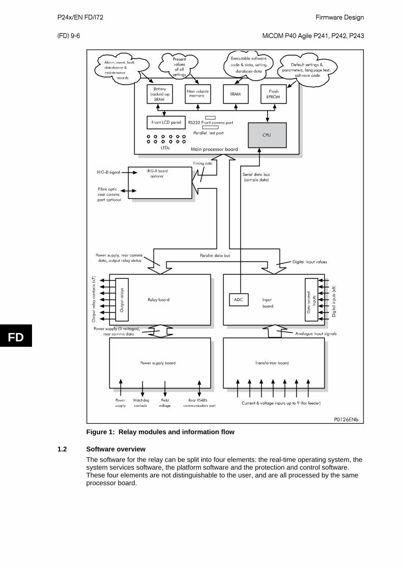
P24x/EN FD/I72
Firmware Design (FD) 9-6 MiCOM P40 Agile P241, P242, P243
FD
Figure 1: Relay modules and information flow
1.2 Software overview The software for the relay can be split into four elements: the real-time operating system, the system services software, the platform software and the protection and control software. These four elements are not distinguishable to the user, and are all processed by the same processor board.

Firmware Design
P24x/EN FD/I72 MiCOM P40 Agile P241, P242, P243 (FD) 9-7
FD
1.2.1 Real-time operating system The real time operating system provides a framework for the different parts of the relay’s software to operate in. The software is split into tasks. The real-time operating system schedules the processing of these tasks so they are carried out at the correct time and in the correct priority. The operating system also exchanges information between tasks in the form of messages.
1.2.2 System services software The system services software provides the low-level control of the relay hardware. For example, the system services software controls the boot of the relay’s software from the non-volatile flash EPROM memory at power-on, and provides driver software for the user interface via the LCD and keypad, and via the serial communication ports. The system services software provides an interface layer between the control of the relay’s hardware and the rest of the relay software.
1.2.3 Platform software The platform software deals with the management of the relay settings, the user interfaces and logging of event, alarm, fault and maintenance records. All of the relay settings are stored in a database within the relay that provides direct compatibility with Courier communications. For all other interfaces (i.e. the front panel keypad and LCD interface, MODBUS and IEC 60870-5-103 and IEC 61850) the platform software converts the information from the database into the format required. The platform software notifies the protection & control software of all settings changes and logs data as specified by the protection & control software.
1.2.4 Protection & control software The protection and control software performs the calculations for all of the protection algorithms of the relay. This includes digital signal processing such as Fourier filtering and ancillary tasks such as the disturbance recorder. The protection & control software interfaces with the platform software for settings changes and logging of records, and with the system services software for acquisition of sample data and access to output relays and digital opto-isolated inputs.
1.2.5 Disturbance recorder The analog values and logic signals are routed from the protection and control software to the disturbance recorder software. The platform software interfaces to the disturbance recorder to allow extraction of the stored records.
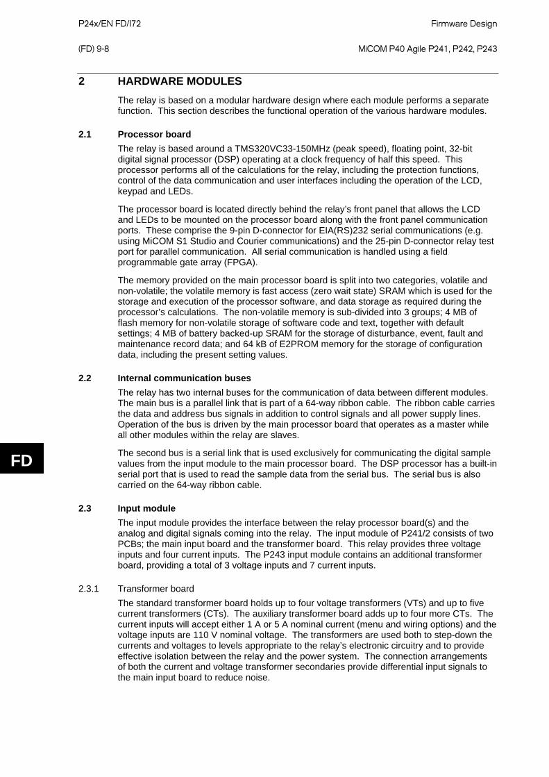
P24x/EN FD/I72
Firmware Design (FD) 9-8 MiCOM P40 Agile P241, P242, P243
FD
2 HARDWARE MODULES The relay is based on a modular hardware design where each module performs a separate function. This section describes the functional operation of the various hardware modules.
2.1 Processor board The relay is based around a TMS320VC33-150MHz (peak speed), floating point, 32-bit digital signal processor (DSP) operating at a clock frequency of half this speed. This processor performs all of the calculations for the relay, including the protection functions, control of the data communication and user interfaces including the operation of the LCD, keypad and LEDs.
The processor board is located directly behind the relay’s front panel that allows the LCD and LEDs to be mounted on the processor board along with the front panel communication ports. These comprise the 9-pin D-connector for EIA(RS)232 serial communications (e.g. using MiCOM S1 Studio and Courier communications) and the 25-pin D-connector relay test port for parallel communication. All serial communication is handled using a field programmable gate array (FPGA).
The memory provided on the main processor board is split into two categories, volatile and non-volatile; the volatile memory is fast access (zero wait state) SRAM which is used for the storage and execution of the processor software, and data storage as required during the processor’s calculations. The non-volatile memory is sub-divided into 3 groups; 4 MB of flash memory for non-volatile storage of software code and text, together with default settings; 4 MB of battery backed-up SRAM for the storage of disturbance, event, fault and maintenance record data; and 64 kB of E2PROM memory for the storage of configuration data, including the present setting values.
2.2 Internal communication buses The relay has two internal buses for the communication of data between different modules. The main bus is a parallel link that is part of a 64-way ribbon cable. The ribbon cable carries the data and address bus signals in addition to control signals and all power supply lines. Operation of the bus is driven by the main processor board that operates as a master while all other modules within the relay are slaves.
The second bus is a serial link that is used exclusively for communicating the digital sample values from the input module to the main processor board. The DSP processor has a built-in serial port that is used to read the sample data from the serial bus. The serial bus is also carried on the 64-way ribbon cable.
2.3 Input module The input module provides the interface between the relay processor board(s) and the analog and digital signals coming into the relay. The input module of P241/2 consists of two PCBs; the main input board and the transformer board. This relay provides three voltage inputs and four current inputs. The P243 input module contains an additional transformer board, providing a total of 3 voltage inputs and 7 current inputs.
2.3.1 Transformer board The standard transformer board holds up to four voltage transformers (VTs) and up to five current transformers (CTs). The auxiliary transformer board adds up to four more CTs. The current inputs will accept either 1 A or 5 A nominal current (menu and wiring options) and the voltage inputs are 110 V nominal voltage. The transformers are used both to step-down the currents and voltages to levels appropriate to the relay’s electronic circuitry and to provide effective isolation between the relay and the power system. The connection arrangements of both the current and voltage transformer secondaries provide differential input signals to the main input board to reduce noise.
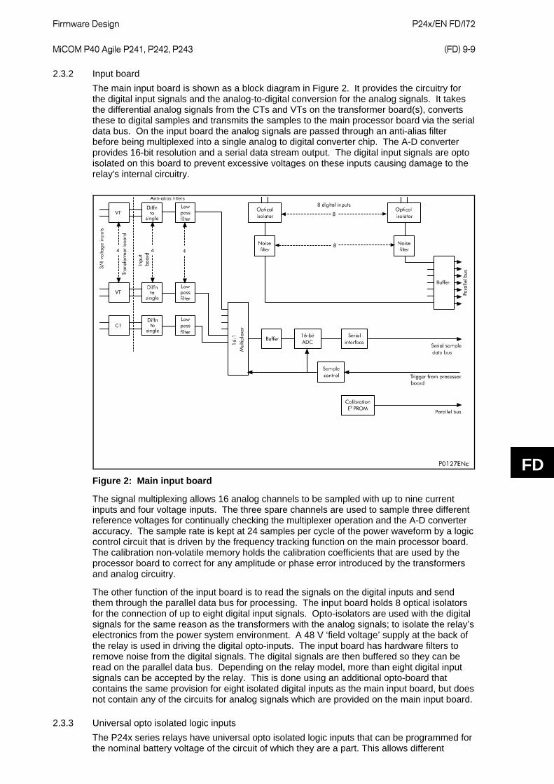
Firmware Design
P24x/EN FD/I72 MiCOM P40 Agile P241, P242, P243 (FD) 9-9
FD
2.3.2 Input board The main input board is shown as a block diagram in Figure 2. It provides the circuitry for the digital input signals and the analog-to-digital conversion for the analog signals. It takes the differential analog signals from the CTs and VTs on the transformer board(s), converts these to digital samples and transmits the samples to the main processor board via the serial data bus. On the input board the analog signals are passed through an anti-alias filter before being multiplexed into a single analog to digital converter chip. The A-D converter provides 16-bit resolution and a serial data stream output. The digital input signals are opto isolated on this board to prevent excessive voltages on these inputs causing damage to the relay's internal circuitry.
Figure 2: Main input board
The signal multiplexing allows 16 analog channels to be sampled with up to nine current inputs and four voltage inputs. The three spare channels are used to sample three different reference voltages for continually checking the multiplexer operation and the A-D converter accuracy. The sample rate is kept at 24 samples per cycle of the power waveform by a logic control circuit that is driven by the frequency tracking function on the main processor board. The calibration non-volatile memory holds the calibration coefficients that are used by the processor board to correct for any amplitude or phase error introduced by the transformers and analog circuitry.
The other function of the input board is to read the signals on the digital inputs and send them through the parallel data bus for processing. The input board holds 8 optical isolators for the connection of up to eight digital input signals. Opto-isolators are used with the digital signals for the same reason as the transformers with the analog signals; to isolate the relay’s electronics from the power system environment. A 48 V ‘field voltage’ supply at the back of the relay is used in driving the digital opto-inputs. The input board has hardware filters to remove noise from the digital signals. The digital signals are then buffered so they can be read on the parallel data bus. Depending on the relay model, more than eight digital input signals can be accepted by the relay. This is done using an additional opto-board that contains the same provision for eight isolated digital inputs as the main input board, but does not contain any of the circuits for analog signals which are provided on the main input board.
2.3.3 Universal opto isolated logic inputs The P24x series relays have universal opto isolated logic inputs that can be programmed for the nominal battery voltage of the circuit of which they are a part. This allows different
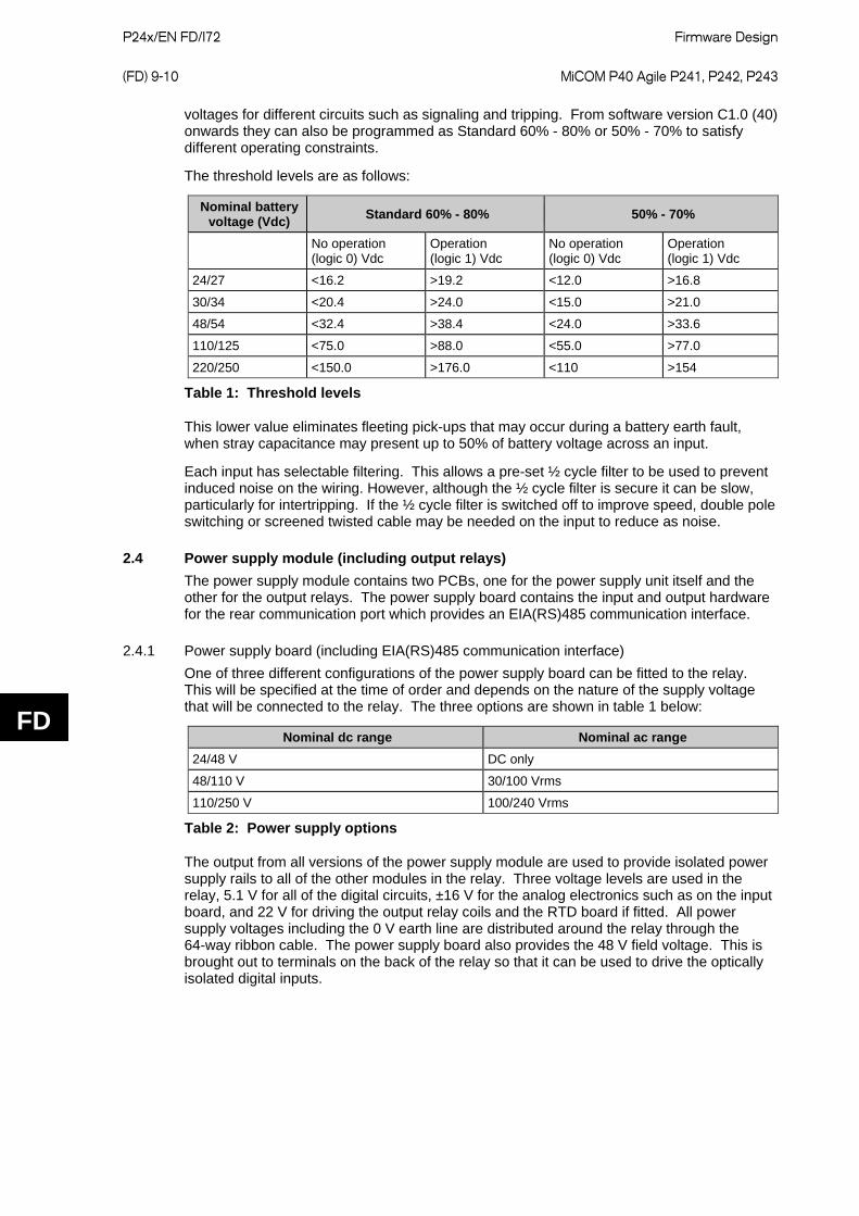
P24x/EN FD/I72
Firmware Design (FD) 9-10 MiCOM P40 Agile P241, P242, P243
FD
voltages for different circuits such as signaling and tripping. From software version C1.0 (40) onwards they can also be programmed as Standard 60% - 80% or 50% - 70% to satisfy different operating constraints.
The threshold levels are as follows:
Nominal battery voltage (Vdc) Standard 60% - 80% 50% - 70%
No operation (logic 0) Vdc
Operation (logic 1) Vdc
No operation (logic 0) Vdc
Operation (logic 1) Vdc
24/27 <16.2 >19.2 <12.0 >16.8
30/34 <20.4 >24.0 <15.0 >21.0
48/54 <32.4 >38.4 <24.0 >33.6
110/125 <75.0 >88.0 <55.0 >77.0
220/250 <150.0 >176.0 <110 >154
Table 1: Threshold levels
This lower value eliminates fleeting pick-ups that may occur during a battery earth fault, when stray capacitance may present up to 50% of battery voltage across an input.
Each input has selectable filtering. This allows a pre-set ½ cycle filter to be used to prevent induced noise on the wiring. However, although the ½ cycle filter is secure it can be slow, particularly for intertripping. If the ½ cycle filter is switched off to improve speed, double pole switching or screened twisted cable may be needed on the input to reduce as noise.
2.4 Power supply module (including output relays) The power supply module contains two PCBs, one for the power supply unit itself and the other for the output relays. The power supply board contains the input and output hardware for the rear communication port which provides an EIA(RS)485 communication interface.
2.4.1 Power supply board (including EIA(RS)485 communication interface) One of three different configurations of the power supply board can be fitted to the relay. This will be specified at the time of order and depends on the nature of the supply voltage that will be connected to the relay. The three options are shown in table 1 below:
Nominal dc range Nominal ac range 24/48 V DC only
48/110 V 30/100 Vrms
110/250 V 100/240 Vrms
Table 2: Power supply options
The output from all versions of the power supply module are used to provide isolated power supply rails to all of the other modules in the relay. Three voltage levels are used in the relay, 5.1 V for all of the digital circuits, ±16 V for the analog electronics such as on the input board, and 22 V for driving the output relay coils and the RTD board if fitted. All power supply voltages including the 0 V earth line are distributed around the relay through the 64-way ribbon cable. The power supply board also provides the 48 V field voltage. This is brought out to terminals on the back of the relay so that it can be used to drive the optically isolated digital inputs.
Firmware Design
P24x/EN FD/I72 MiCOM P40 Agile P241, P242, P243 (FD) 9-11
FD
The two other functions provided by the power supply board are the EIA(RS)485 communications interface and the watchdog contacts for the relay. The EIA(RS)485 interface is used with the relay’s rear communication port to provide communication using one of either Courier, MODBUS, or IEC 60870-5-103 protocols. The EIA(RS)485 hardware supports half-duplex communication and provides optical isolation of the serial data that is transmitted and received. All internal communication of data from the power supply board is through the output relay board connected to the parallel bus.
The watchdog facility has two output relay contacts, one normally open and one normally closed. These are driven by the main processor board and indicate that the relay is in a healthy state.
The power supply board incorporates inrush current limiting. This limits the peak inrush current, during energization, to approximately 10 A.
2.4.2 Output relay board There are 2 versions of the output relay board:
• Seven relays, three normally open contacts and four changeover contacts • Eight relays, six normally open contacts and two changeover contacts. For relay models with suffix A hardware, only 7 output relay boards are available. For relay models with suffix C hardware or greater the base numbers of output contacts, using the 7 output relay boards, is maintained for compatibility. The 8 output relay board is used for new relay models or existing relay models available in new case sizes or to provide additional output contacts to existing models for suffix issue C or greater hardware.
Note: The model number suffix letter refers to the hardware version.
The relays are driven from the 22 V power supply line. The relays’ state is written to or read from using the parallel data bus. Depending on the relay model, more than seven output contacts may be provided, through the use of up to three extra relay boards. Each additional relay board provides a further seven or eight output relays.
2.5 RTD board The RTD (Resistance Temperature Detector) board is an order option. It is used to monitor the temperature readings from up to ten PT100 RTDs that are each connected using a 3-wire connection. The board is powered from the 22 V power rail that is used to drive the output relays. The RTD board includes two redundant channels that are connected to high stability resistors to provide reference readings. These are used to check the operation of the RTD board. The temperature data is read by the processor through the parallel data bus, and is used to provide thermal protection of the generator windings.
2.6 IRIG-B board The IRIG-B board can be fitted to provide an accurate timing reference for the device. The IRIG-B signal is connected to the board via a BNC connector. The timing information is used to synchronise the IED's internal real-time clock to an accuracy of 1 ms. The internal clock is then used for time tagging events, fault, maintenance and disturbance records.
IRIG-B interface is available in modulated or demodulated formats.
The IRIG-B facility is provided in combination with other functionality on a number of additional boards, such as:
• Fibre board with IRIG-B • Second rear communications board with IRIG-B • Ethernet board with IRIG-B • Redundant Ethernet board with IRIG-B
2.7 Second rear communications board For relays with Courier, MODBUS, or IEC 60870-5-103 protocol on the first rear communications port there is the hardware option of a second rear communications port, which runs the Courier language. This can be used over one of three physical links: twisted
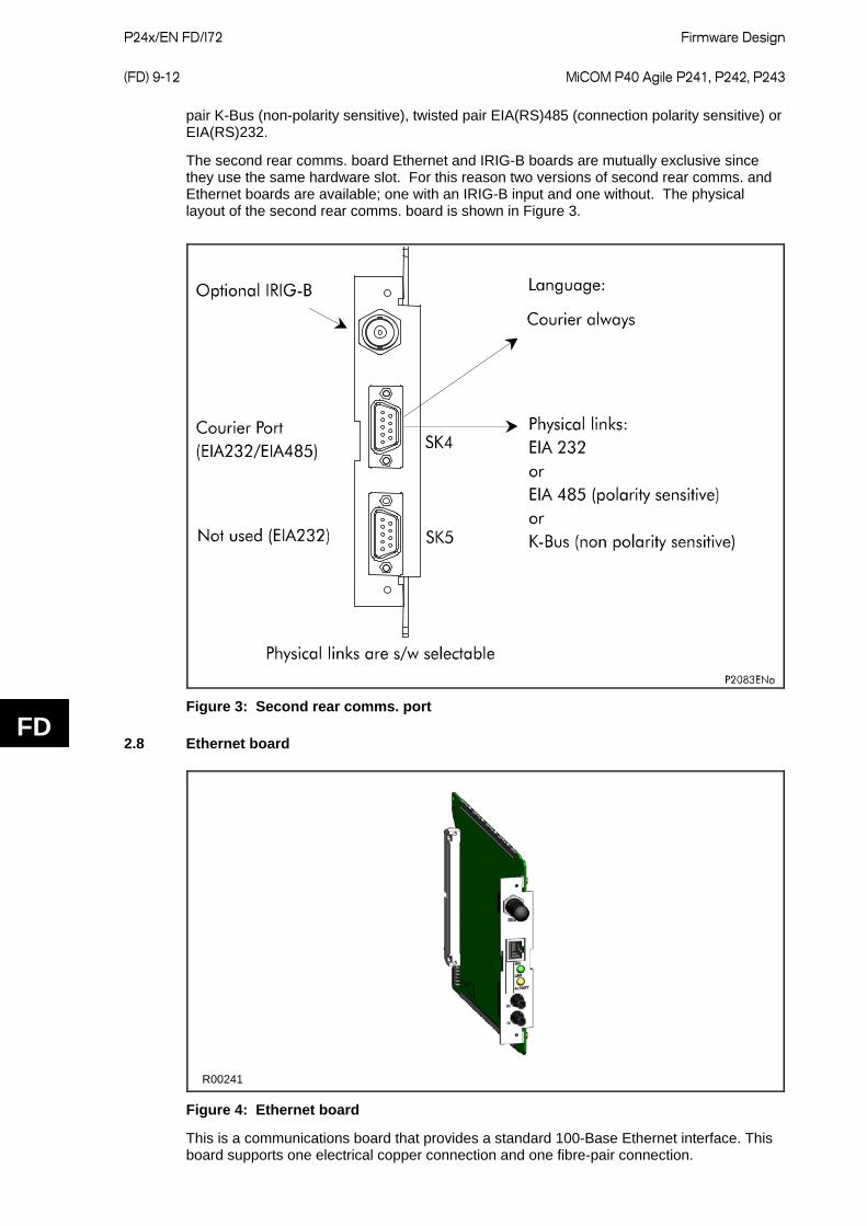
P24x/EN FD/I72
Firmware Design (FD) 9-12 MiCOM P40 Agile P241, P242, P243
FD
pair K-Bus (non-polarity sensitive), twisted pair EIA(RS)485 (connection polarity sensitive) or EIA(RS)232.
The second rear comms. board Ethernet and IRIG-B boards are mutually exclusive since they use the same hardware slot. For this reason two versions of second rear comms. and Ethernet boards are available; one with an IRIG-B input and one without. The physical layout of the second rear comms. board is shown in Figure 3.
Figure 3: Second rear comms. port
2.8 Ethernet board
R00241
Figure 4: Ethernet board
This is a communications board that provides a standard 100-Base Ethernet interface. This board supports one electrical copper connection and one fibre-pair connection.
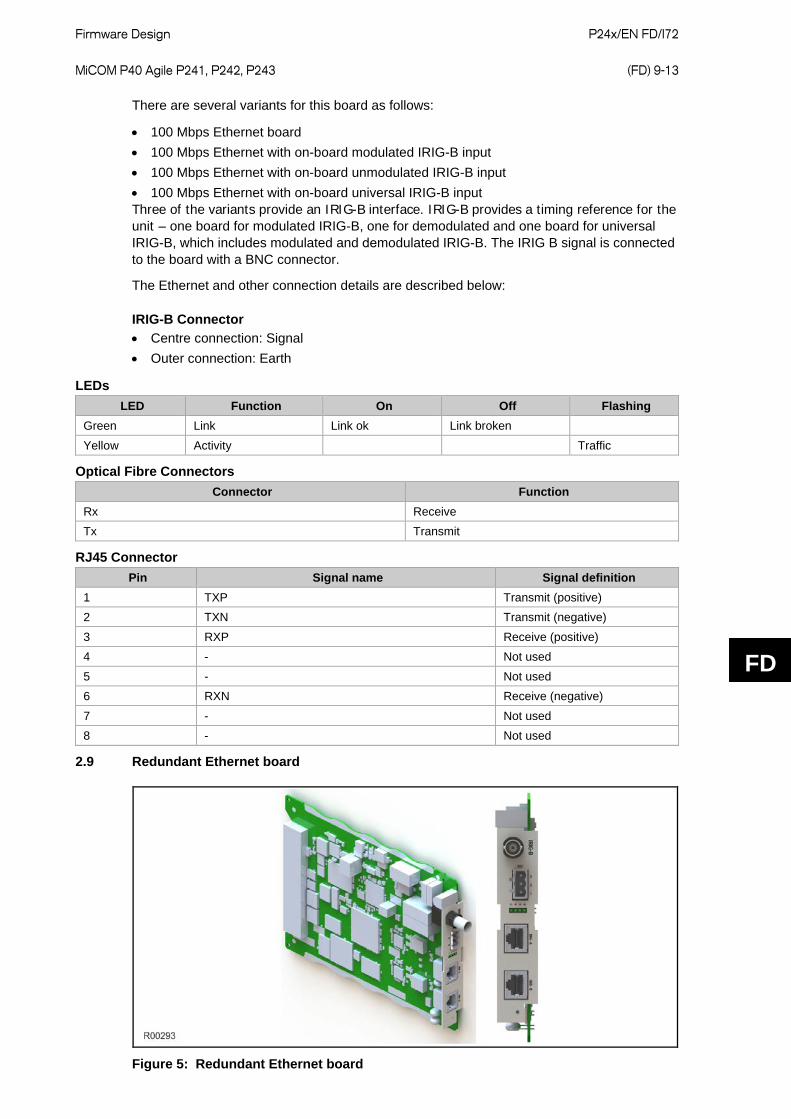
Firmware Design P24x/EN FD/I72
MiCOM P40 Agile P241, P242, P243 (FD) 9-13
FD
There are several variants for this board as follows:
• 100 Mbps Ethernet board• 100 Mbps Ethernet with on-board modulated IRIG-B input• 100 Mbps Ethernet with on-board unmodulated IRIG-B input• 100 Mbps Ethernet with on-board universal IRIG-B inputThree of the variants provide an IRIG-B interface. IRIG-B provides a timing reference for the unit – one board for modulated IRIG-B, one for demodulated and one board for universal IRIG-B, which includes modulated and demodulated IRIG-B. The IRIG B signal is connected to the board with a BNC connector.
The Ethernet and other connection details are described below:
IRIG-B Connector • Centre connection: Signal• Outer connection: Earth
LEDs LED Function On Off Flashing
Green Link Link ok Link broken Yellow Activity Traffic
Optical Fibre Connectors Connector Function
Rx Receive Tx Transmit
RJ45 Connector Pin Signal name Signal definition
1 TXP Transmit (positive) 2 TXN Transmit (negative) 3 RXP Receive (positive) 4 - Not used 5 - Not used 6 RXN Receive (negative) 7 - Not used 8 - Not used
2.9 Redundant Ethernet board
Figure 5: Redundant Ethernet board
P24x/EN FD/I72
Firmware Design (FD) 9-14 MiCOM P40 Agile P241, P242, P243
FD
This board provides dual redundant Ethernet (supported by two fibre pairs) together with an IRIG-B interface for timing.
Different board variants are available, depending on the redundancy protocol and the type of IRIG-B signal (unmodulated or modulated). The available redundancy protocols are:
• SHP (Self-Healing Protocol) • RSTP (Rapid Spanning Tree Protocol) • DHP (Dual Homing Protocol) • PRP (Parallel Redundancy Protocol) • HSR (High-availability Seamless Redundancy) There are several variants for this board as follows:
• 100 Mbps redundant Ethernet running RSTP, with on-board modulated IRIG-B • 100 Mbps redundant Ethernet running RSTP, with on-board unmodulated IRIG-B • 100 Mbps redundant Ethernet running SHP, with on-board modulated IRIG-B • 100 Mbps redundant Ethernet running SHP, with on-board unmodulated IRIG-B • 100 Mbps redundant Ethernet running DHP, with on-board modulated IRIG-B • 100 Mbps redundant Ethernet running DHP, with on-board unmodulated IRIG-B • 100 Mbps redundant Ethernet running PRP + HSR, with on-board modulated IRIG-B • 100 Mbps redundant Ethernet running PRP + HSR, with on-board demodulated IRIG-B • 100 Mbps redundant Ethernet running RSTP + PRP + HSR (two fibre pairs), with on-
board universal IRIG-B • 100 Mbps redundant Ethernet running RSTP + PRP + HSR (two copper pairs), with on-
board universal IRIG-B The Ethernet and other connection details are described below:
IRIG-B Connector • Centre connection: Signal • Outer connection: Earth
Link Fail Connector (Ethernet Board Watchdog Relay) Pin Closed Open
1-2 Link fail Channel 1 (A) Link ok Channel 1 (A)
2-3 Link fail Channel 2 (B) Link ok Channel 2 (B)
LEDs LED Function On Off Flashing
Green Link Link ok Link broken
Yellow Activity SHP running PRP, RSTP or DHP traffic
Optical Fibre Connectors (ST) Connector DHP RSTP SHP PRP
A RXA RX1 RS RXA
B TXA TX1 ES TXA
C RXB RX2 RP RXB
D TXB TX2 EP TXB
RJ45 Connector Pin Signal name Signal definition
1 TXP Transmit (positive) 2 TXN Transmit (negative) 3 RXP Receive (positive)
Firmware Design
P24x/EN FD/I72 MiCOM P40 Agile P241, P242, P243 (FD) 9-15
FD
Pin Signal name Signal definition 4 - Not used 5 - Not used 6 RXN Receive (negative) 7 - Not used 8 - Not used
2.10 Current loop input output board (CLIO) The current loop input output (CLIO) board is an order option. The CLIO board is powered from the 22 V power rail that is used to drive the output relays.
Four analog (or current loop) inputs are provided for transducers with ranges of 0 - 1 mA, 0 - 10 mA, 0 - 20 mA or 4 - 20 mA. The input current data is read by the processor through the parallel data bus, and is used to provide measurements from various transducers such as vibration monitors, tachometers and pressure transducers.
For each of the four current loop inputs there are two separate input circuits, 0 - 1 mA and 0 - 20 mA. The latter is also used for 0 - 10 mA and 4 - 20 mA transducer inputs. The anti-alias filters have a nominal cut-off frequency (3 dB point) of 23 Hz to reduce power system interference from the incoming signals. Four analog current outputs are provided with ranges of 0 - 1 mA, 0 - 10 mA, 0 - 20 mA or 4 - 20 mA which can alleviate the need for separate transducers. These may be used to feed standard moving coil ammeters for analog indication of certain measured quantities or into a SCADA using an existing analog RTU.
Each of the four current loop outputs provides one 0 - 1 mA output, one 0 - 20 mA output and one common return. Suitable software scaling of the value written to the board allows the 0 - 20 mA output to also provide 0 - 10 mA and 4 - 20 mA. Screened leads are recommended for use on the current loop output circuits. The refresh interval for the outputs is nominally 200 ms.
All external connections to the current loop I/O board are made using the same 15 way light duty I/O connector SL3.5/15/90F used on the RTD board. Two such connectors are used, one for the current loop outputs and one for the current loop inputs.
The I/O connectors accommodate wire sizes in the range 1/0.85 mm (0.57 mm2) to 1/1.38 mm (1.5 mm2) and their multiple conductor equivalents. The use of screened cable is recommended. The screen terminations should be connected to the case earth of the relay.
Basic Insulation (300 V) is provided between analog inputs or outputs and earth and between analog inputs and outputs. However, there is no insulation between one input and another or one output and another.
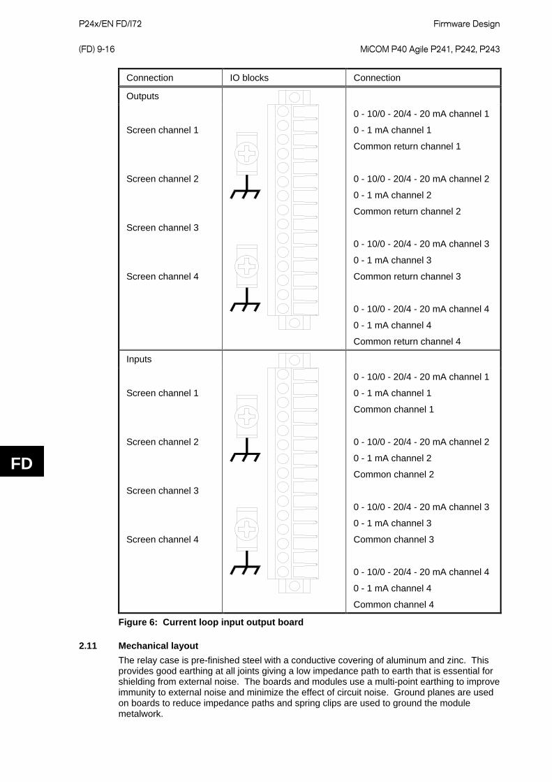
P24x/EN FD/I72
Firmware Design (FD) 9-16 MiCOM P40 Agile P241, P242, P243
FD
Connection IO blocks Connection
Outputs
Screen channel 1
Screen channel 2
Screen channel 3
Screen channel 4
0 - 10/0 - 20/4 - 20 mA channel 1
0 - 1 mA channel 1
Common return channel 1
0 - 10/0 - 20/4 - 20 mA channel 2
0 - 1 mA channel 2
Common return channel 2
0 - 10/0 - 20/4 - 20 mA channel 3
0 - 1 mA channel 3
Common return channel 3
0 - 10/0 - 20/4 - 20 mA channel 4
0 - 1 mA channel 4
Common return channel 4
Inputs
Screen channel 1
Screen channel 2
Screen channel 3
Screen channel 4
0 - 10/0 - 20/4 - 20 mA channel 1
0 - 1 mA channel 1
Common channel 1
0 - 10/0 - 20/4 - 20 mA channel 2
0 - 1 mA channel 2
Common channel 2
0 - 10/0 - 20/4 - 20 mA channel 3
0 - 1 mA channel 3
Common channel 3
0 - 10/0 - 20/4 - 20 mA channel 4
0 - 1 mA channel 4
Common channel 4
Figure 6: Current loop input output board
2.11 Mechanical layout The relay case is pre-finished steel with a conductive covering of aluminum and zinc. This provides good earthing at all joints giving a low impedance path to earth that is essential for shielding from external noise. The boards and modules use a multi-point earthing to improve immunity to external noise and minimize the effect of circuit noise. Ground planes are used on boards to reduce impedance paths and spring clips are used to ground the module metalwork.

Firmware Design
P24x/EN FD/I72 MiCOM P40 Agile P241, P242, P243 (FD) 9-17
FD
Heavy duty terminal blocks are used at the rear of the relay for the current and voltage signal connections. Medium duty terminal blocks are used for the digital logic input signals, output relay contacts, power supply and rear communication port. A BNC connector is used for the optional IRIG-B signal. 9-pin and 25-pin female D-connectors are used at the front of the relay for data communication.
Inside the relay the PCBs plug into the connector blocks at the rear, and can be removed from the front of the relay only. The connector blocks to the relay’s CT inputs have internal shorting links inside the relay. These automatically short the current transformer circuits before they are broken when the board is removed.
The front panel consists of a membrane keypad with tactile dome keys, an LCD and 12 LEDs mounted on an aluminum backing plate.
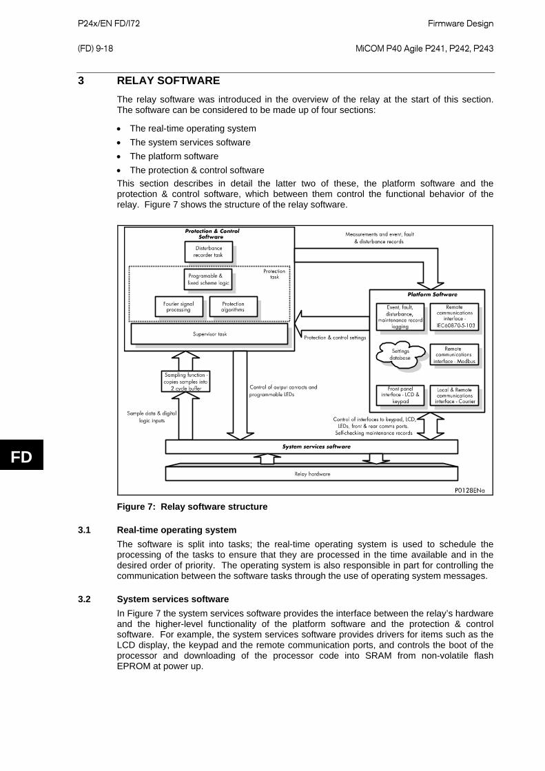
P24x/EN FD/I72
Firmware Design (FD) 9-18 MiCOM P40 Agile P241, P242, P243
FD
3 RELAY SOFTWARE The relay software was introduced in the overview of the relay at the start of this section. The software can be considered to be made up of four sections:
• The real-time operating system • The system services software • The platform software • The protection & control software This section describes in detail the latter two of these, the platform software and the protection & control software, which between them control the functional behavior of the relay. Figure 7 shows the structure of the relay software.
Figure 7: Relay software structure
3.1 Real-time operating system The software is split into tasks; the real-time operating system is used to schedule the processing of the tasks to ensure that they are processed in the time available and in the desired order of priority. The operating system is also responsible in part for controlling the communication between the software tasks through the use of operating system messages.
3.2 System services software In Figure 7 the system services software provides the interface between the relay’s hardware and the higher-level functionality of the platform software and the protection & control software. For example, the system services software provides drivers for items such as the LCD display, the keypad and the remote communication ports, and controls the boot of the processor and downloading of the processor code into SRAM from non-volatile flash EPROM at power up.

Firmware Design
P24x/EN FD/I72 MiCOM P40 Agile P241, P242, P243 (FD) 9-19
FD
3.3 Platform software The platform software has three main functions:
• To control the logging of all records that are generated by the protection software, including alarms and event, fault, disturbance and maintenance records.
• To store and maintain a database of all of the relay’s settings in non-volatile memory. • To provide the internal interface between the settings database and each of the relay’s
user interfaces, i.e. the front panel interface and the front and rear communication ports, using whichever communication protocol has been specified (Courier, MODBUS and IEC 60870-5-103).
3.3.1 Record logging The logging function is provided to store all alarms, events, faults and maintenance records. The records for all of these incidents are logged in battery backed-up SRAM to provide a non-volatile log of what has happened. The relay maintains four logs: one each for up to 32 alarms, 250 event records, 5 fault records and 5 maintenance records. The logs are maintained such that the oldest record is overwritten with the newest record. The logging function can be initiated from the protection software or the platform software.
The logging function can be initiated from the protection software or the platform software is responsible for logging of a maintenance record in the event of a relay failure. This includes errors that have been detected by the platform software itself or error that are detected by either the system services or the protection software functions. See also the section on supervision and diagnostics later in this chapter.
3.3.2 Settings database The settings database contains all of the settings and data for the relay, including the protection, disturbance recorder and control & support settings. The settings are maintained in non-volatile memory. The platform software’s management of the settings database includes the responsibility of ensuring that only one user interface modifies the settings of the database at any one time. This feature is employed to avoid confusion between different parts of the software during a setting change. For changes to protection settings and disturbance recorder settings, the platform software operates a ‘scratchpad’ in SRAM memory. This allows a number of setting changes to be made in any order but applied to the protection elements, disturbance recorder and saved in the database in non-volatile memory, at the same time. If a setting change affects the protection & control task, the database advises it of the new values.
3.3.3 Database interface The other function of the platform software is to implement the relay’s internal interface between the database and each of the relay’s user interfaces. The database of settings and measurements must be accessible from all of the relay’s user interfaces to allow read and modify operations. The platform software presents the data in the appropriate format for each user interface.
3.4 Protection and control software The protection and control software task processes all of the protection elements and measurement functions of the relay. It has to communicate with both the system services software and the platform software as well as organize its own operations. The protection software has the highest priority of any of the software tasks in the relay to provide the fastest possible protection response. The protection & control software has a supervisor task that controls the start-up of the task and deals with the exchange of messages between the task and the platform software.
P24x/EN FD/I72
Firmware Design (FD) 9-20 MiCOM P40 Agile P241, P242, P243
FD
3.4.1 Overview - protection and control scheduling After initialization at start-up, the protection & control task waits until there are enough samples to process. The sampling function is called by the system services software and takes each set of new samples from the input module and stores them in a two-cycle buffer. The protection & control software resumes execution when the number of unprocessed samples in the buffer reaches a certain number. For the P24x motor protection relays, the protection task is executed four times per cycle, i.e. after every 2 samples for the sample rate of 24 samples per power cycle used by the relay. The protection elements are split into groups so that different elements are processed each time, and every element is processed at least once per cycle. The protection and control software is suspended again when all of its processing on a set of samples is complete. This allows operations by other software tasks to take place.
3.4.2 Signal processing The sampling function filters the digital input signals from the opto-isolators and tracks the frequency of the analog signals. The digital inputs are checked against their previous value over a period of half a cycle. Therefore, a change in the state of one of the inputs must be maintained over at least half a cycle before it is registered with the protection & control software.
The frequency tracking of the analog input signals is achieved by a recursive Fourier algorithm which is applied to one of the input signals, and works by detecting a change in the measured signal’s phase angle. The calculated value of the frequency is used to modify the sample rate being used by the input module so as to achieve a constant sample rate of 24 samples per cycle of the power waveform. The value of the frequency is also stored for use by the protection & control task.
When the protection & control task is re-started by the sampling function, it calculates the Fourier components for the analog signals. The Fourier components are calculated using a one-cycle, 24-sample Discrete Fourier Transform (DFT). The DFT is always calculated using the last cycle of samples from the 2-cycle buffer, i.e. the most recent data is used. The DFT used in this way extracts the power frequency fundamental component from the signal and produces the magnitude and phase angle of the fundamental in rectangular component format. The DFT provides an accurate measurement of the fundamental frequency component, and effective filtering of harmonic frequencies and noise. This performance is achieved in conjunction with the relay input module which provides hardware anti-alias filtering to attenuate frequencies above the half sample rate, and frequency tracking to maintain a sample rate of 24 samples per cycle. The Fourier components of the input current and voltage signals are stored in memory so that they can be accessed by all of the protection elements’ algorithms. The samples from the input module are also used in an unprocessed form by the disturbance recorder for waveform recording and to calculate true rms values of current, voltage and power for metering purposes.
3.4.3 Frequency response With the exception of the RMS measurements all other measurements and protection functions are based on the Fourier derived fundamental component. The fundamental component is extracted by using a 24 sample Discrete Fourier Transform (DFT). This gives good harmonic rejection for frequencies up to the 23rd harmonic. The 23rd is the first predominant harmonic that is not attenuated by the Fourier filter and this is known as an ‘Alias’. However, the Alias is attenuated by approximately 85% by an additional, analog, ‘anti-aliasing’ filter (low pass filter). The combined affect of the anti-aliasing and Fourier filters is shown below:
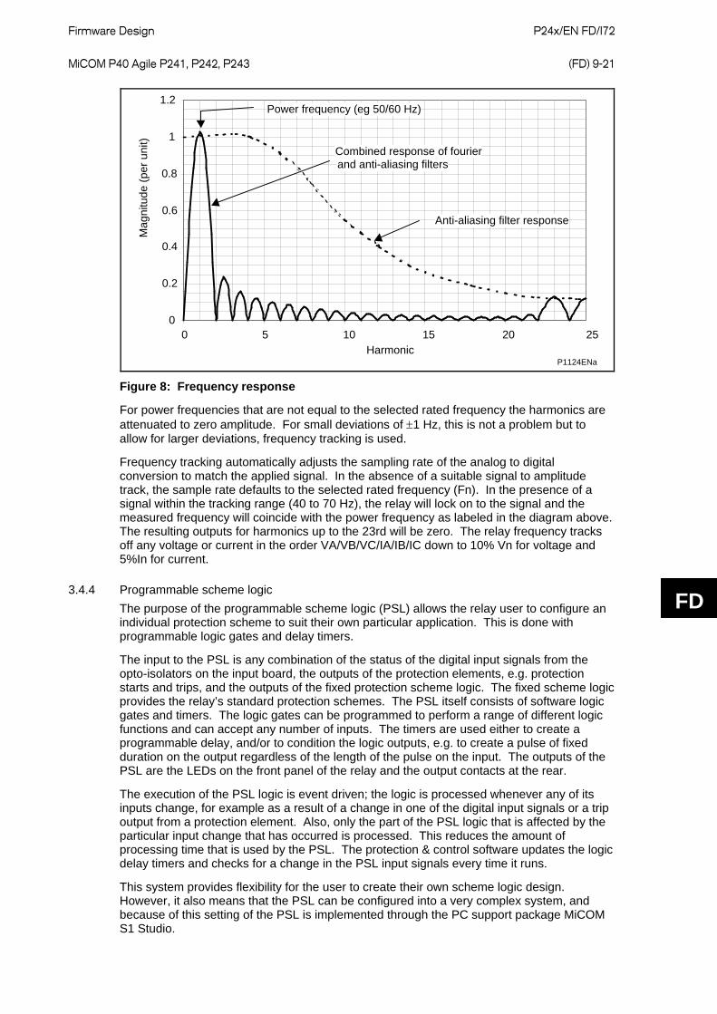
Firmware Design
P24x/EN FD/I72 MiCOM P40 Agile P241, P242, P243 (FD) 9-21
FD
0
0.2
0.4
0.6
0.8
1
1.2
0 5 10 15 20 25Harmonic
Mag
nitu
de (p
er u
nit)
Combined response of fourier and anti-aliasing filters
Anti-aliasing filter response
Power frequency (eg 50/60 Hz)
P1124ENa
Figure 8: Frequency response
For power frequencies that are not equal to the selected rated frequency the harmonics are attenuated to zero amplitude. For small deviations of ±1 Hz, this is not a problem but to allow for larger deviations, frequency tracking is used.
Frequency tracking automatically adjusts the sampling rate of the analog to digital conversion to match the applied signal. In the absence of a suitable signal to amplitude track, the sample rate defaults to the selected rated frequency (Fn). In the presence of a signal within the tracking range (40 to 70 Hz), the relay will lock on to the signal and the measured frequency will coincide with the power frequency as labeled in the diagram above. The resulting outputs for harmonics up to the 23rd will be zero. The relay frequency tracks off any voltage or current in the order VA/VB/VC/IA/IB/IC down to 10% Vn for voltage and 5%In for current.
3.4.4 Programmable scheme logic The purpose of the programmable scheme logic (PSL) allows the relay user to configure an individual protection scheme to suit their own particular application. This is done with programmable logic gates and delay timers.
The input to the PSL is any combination of the status of the digital input signals from the opto-isolators on the input board, the outputs of the protection elements, e.g. protection starts and trips, and the outputs of the fixed protection scheme logic. The fixed scheme logic provides the relay’s standard protection schemes. The PSL itself consists of software logic gates and timers. The logic gates can be programmed to perform a range of different logic functions and can accept any number of inputs. The timers are used either to create a programmable delay, and/or to condition the logic outputs, e.g. to create a pulse of fixed duration on the output regardless of the length of the pulse on the input. The outputs of the PSL are the LEDs on the front panel of the relay and the output contacts at the rear.
The execution of the PSL logic is event driven; the logic is processed whenever any of its inputs change, for example as a result of a change in one of the digital input signals or a trip output from a protection element. Also, only the part of the PSL logic that is affected by the particular input change that has occurred is processed. This reduces the amount of processing time that is used by the PSL. The protection & control software updates the logic delay timers and checks for a change in the PSL input signals every time it runs.
This system provides flexibility for the user to create their own scheme logic design. However, it also means that the PSL can be configured into a very complex system, and because of this setting of the PSL is implemented through the PC support package MiCOM S1 Studio.
P24x/EN FD/I72
Firmware Design (FD) 9-22 MiCOM P40 Agile P241, P242, P243
FD
3.4.5 Function key interface (P242/3 only) The ten function keys interface directly into the PSL as digital input signals and are processed based on the PSL’s event driven execution. However, a change of state is only recognized when a key press is executed on average for longer than 200 ms. The time to register a change of state depends on whether the function key press is executed at the start or the end of a protection task cycle, with the additional hardware and software scan time included. A function key press can provide a latched (toggled mode) or output on key press only (normal mode) depending on how it is programmed and can be configured to individual protection scheme requirements. The latched state signal for each function key is written to non-volatile memory and read from non-volatile memory during relay power up, allowing the function key state to be reinstated after power-up if the relay power is lost.
3.4.6 Event, fault & maintenance recording A change in any digital input signal or protection element output signal is used to indicate that an event has taken place. When this happens, the protection & control task sends a message to the supervisor task to indicate that an event is available to be processed and writes the event data to a fast buffer in SRAM that is controlled by the supervisor task. When the supervisor task receives either an event or fault record message, it instructs the platform software to create the appropriate log in battery backed-up SRAM. The operation of the record logging to battery backed-up SRAM is slower than the supervisor’s buffer. This means that the protection software is not delayed waiting for the records to be logged by the platform software. However, in the rare case when a large number of records to be logged are created in a short period of time, it is possible that some will be lost, if the supervisor’s buffer is full before the platform software is able to create a new log in battery backed-up SRAM. If this occurs then an event is logged to indicate this loss of information.
Maintenance records are created in a similar manner with the supervisor task instructing the platform software to log a record when it receives a maintenance record message. However, it is possible that a maintenance record may be triggered by a fatal error in the relay in which case it may not be possible to successfully store a maintenance record, depending on the nature of the problem. See self supervision & diagnostics later in this chapter.
3.4.7 Disturbance recorder The disturbance recorder operates as a separate task from the protection and control task. It can record the waveforms for up to 8 analog channels and the values of up to 32 digital signals. The recording time is user selectable up to a maximum of 10 seconds. The disturbance recorder is supplied with data by the protection and control task once per cycle. The disturbance recorder collates the data that it receives into the required length disturbance record. The disturbance records can be extracted by MiCOM S1 Studio that can also store the data in COMTRADE format, therefore allowing the use of other packages to view the recorded data.

Firmware Design
P24x/EN FD/I72 MiCOM P40 Agile P241, P242, P243 (FD) 9-23
FD
4 SELF TESTING & DIAGNOSTICS The relay includes several self-monitoring functions to check the operation of its hardware and software when it is in service. These are included so that if an error or fault occurs in the relay’s hardware or software, the relay is able to detect and report the problem and attempt to resolve it by performing a re-boot. The relay must therefore be out of service for a short time, during which the Healthy LED on the front of the relay is OFF and, the watchdog contact at the rear is ON. If the reboot fails to resolve the problem, the relay takes itself permanently out of service; the Healthy LED stays OFF and watchdog contact stays ON.
If a problem is detected by the self-monitoring functions, the relay stores a maintenance record in battery backed-up SRAM.
The self-monitoring is implemented in two stages: firstly a thorough diagnostic check that is performed when the relay is booted-up and secondly a continuous self-checking operation that checks the operation of the relay’s critical functions while it is in service.
4.1 Start-up self-testing The self-testing that is carried out when the relay is started takes a few seconds to complete, during which time the relay’s protection is unavailable. This is shown by the Healthy LED on the front of the relay which is ON when the relay has passed all tests and entered operation. If the tests detect a problem, the relay remains out of service until it is manually restored to working order.
The operations that are performed at start-up are as follows:
4.1.1 System boot The integrity of the flash EPROM memory is verified using a checksum before the program code and data stored in it is copied into SRAM to be used for execution by the processor. When the copy is complete the data then held in SRAM is checked against that in flash EPROM to ensure they are the same and that no errors have occurred in the transfer of data from flash EPROM to SRAM. The entry point of the software code in SRAM is then called which is the relay initialization code.
4.1.2 Initialization software The initialization process includes the operations of initializing the processor registers and interrupts, starting the watchdog timers (used by the hardware to determine whether the software is still running), starting the real-time operating system and creating and starting the supervisor task. In the course of the initialization process the relay checks:
• The status of the battery • The integrity of the battery backed-up SRAM that is used to store event, fault and
disturbance records • The voltage level of the field voltage supply that is used to drive the opto-isolated inputs • The operation of the LCD controller • The watchdog operation At the conclusion of the initialization software the supervisor task begins the process of starting the platform software.
4.1.3 Platform software initialization & monitoring In starting the platform software, the relay checks the integrity of the data held in non-volatile memory with a checksum, the operation of the real-time clock, and the IRIG-B, RTD and CLIO board if fitted. The final test that is made concerns the input and output of data; the presence and healthy condition of the input board is checked and the analog data acquisition system is checked through sampling the reference voltage.
At the successful conclusion of all of these tests the relay is entered into service and the protection started-up.

P24x/EN FD/I72
Firmware Design (FD) 9-24 MiCOM P40 Agile P241, P242, P243
FD
4.2 Continuous self-testing When the relay is in service, it continually checks the operation of the critical parts of its hardware and software. The checking is carried out by the system services software (see section on relay software earlier in this section) and the results reported to the platform software. The functions that are checked are as follows:
• The flash EPROM containing all program code and language text is verified by a checksum
• The code and constant data held in SRAM is checked against the corresponding data in flash EPROM to check for data corruption
• The SRAM containing all data other than the code and constant data is verified with a checksum
• The non-volatile memory containing setting values is verified by a checksum, whenever its data is accessed
• The battery status • The level of the field voltage • The integrity of the digital signal I/O data from the opto-isolated inputs and the relay
contacts, is checked by the data acquisition function every time it is executed. The operation of the analog data acquisition system is continuously checked by the acquisition function every time it is executed, by means of sampling the reference voltage on a spare multiplexed channel
• The operation of the RTD board is checked by reading the temperature indicated by the reference resistors on the two spare RTD channels
• The operation of the IRIG-B board is checked, where it is fitted, by the software that reads the time and date from the board
• The correct operation of the CLIO board is checked, where it is fitted • The operation of the Ethernet board is checked, where it is fitted, by the software on the
main processor card. If the Ethernet board fails to respond an alarm is raised and the card is reset in an attempt to resolve the problem
In the unlikely event that one of the checks detects an error in the relay’s subsystems, the platform software is notified and it will attempt to log a maintenance record in battery backed-up SRAM. If the problem is with the battery status, the RTD board, CLIO board or the IRIG-B board, the relay continues in operation. However, for problems detected in any other area the relay shuts down and reboots. This result in a period of up to 5 seconds when protection is unavailable, but the complete restart of the relay including all initializations should clear most problems that could occur. An integral part of the start-up procedure is a thorough diagnostic self-check. If this detects the same problem that caused the relay to restart, the restart has not cleared the problem, and the relay takes itself permanently out of service. This is indicated by the Healthy LED on the front of the relay, which goes OFF, and the watchdog contact that goes ON.
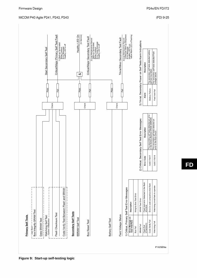
Firmware Design
P24x/EN FD/I72 MiCOM P40 Agile P241, P242, P243 (FD) 9-25
FD
Figure 9: Start-up self-testing logic
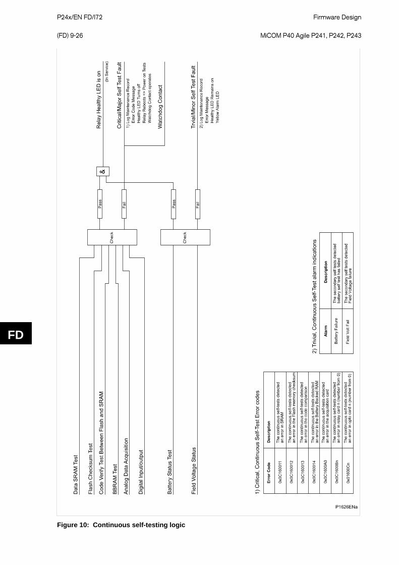
P24x/EN FD/I72
Firmware Design (FD) 9-26 MiCOM P40 Agile P241, P242, P243
FD
Figure 10: Continuous self-testing logic

Commissioning
P24x/EN CM/I72 MiCOM P40 Agile P241, P242, P243 (CM) 10-1
CM
COMMISSIONING

P24x/EN CM/I72
Commissioning (CM) 10-2 MiCOM P40 Agile P241, P242, P243
CM
Commissioning
P24x/EN CM/I72 MiCOM P40 Agile P241, P242, P243 (CM) 10-3
CM
CONTENTS
1 INTRODUCTION 7
2 SETTING FAMILIARIZATION 8
3 COMMISSIONING TEST MENU 9
3.1 Opto I/P status 10
3.2 Relay O/P status 10
3.3 Test port status 10
3.4 LED status 10
3.5 Monitor bits 1 to 8 10
3.6 Test mode 11
3.7 Test pattern 11
3.8 Contact test 11
3.9 Test LEDs 11
3.10 Red LED status and green LED status (P242/3) 11
3.11 Using a monitor/download port test box 11
4 EQUIPMENT REQUIRED FOR COMMISSIONING 12
4.1 Minimum equipment required 12
4.2 Optional equipment 12
5 PRODUCT CHECKS 13
5.1 With the relay re-energized 13
5.1.1 Visual inspection 14
5.1.2 Current transformer shorting contacts 14
5.1.3 Insulation 15
5.1.4 External wiring 16
5.1.5 Watchdog contacts 16
5.1.6 Auxiliary supply 16
5.2 With the relay energized 17
5.2.1 Watchdog contacts 17
5.2.2 LCD front panel display 17
5.2.3 Date and time 17
5.2.3.1 With an IRIG-B signal 17
5.2.3.2 Without an IRIG-B signal 18
5.2.4 Light emitting diodes (LEDs) 18
5.2.4.1 Testing the alarm and out of service LEDs 18
5.2.4.2 Testing the trip LED 18
5.2.4.3 Testing the user-programmable LEDs 18
5.2.5 Field voltage supply 18
5.2.6 Input opto-isolators 19
5.2.7 Output relays 19
P24x/EN CM/I72
Commissioning (CM) 10-4 MiCOM P40 Agile P241, P242, P243
CM
5.2.8 RTD inputs 20
5.2.9 Current loop inputs 20
5.2.10 Current loop (analog) outputs 21
5.2.11 First rear communications port 21
5.2.11.1 Courier communications 21
5.2.11.2 MODBUS communications 22
5.2.11.3 IEC 60870-5-103 (VDEW) communications 22
5.2.11.4 IEC 61850 communications 22
5.2.12 Second rear communications port 23
5.2.12.1 K-Bus configuration 23
5.2.12.2 EIA(RS)485 configuration 24
5.2.12.3 EIA(RS)232 configuration 24
5.2.13 Current inputs 24
5.2.14 Voltage inputs 26
6 SETTING CHECKS 27
6.1 Apply application-specific settings 27
6.2 Check application-specific settings 27
6.3 Demonstrate correct relay operation 28
6.3.1 Motor differential protection (P243) 28
6.3.1.1 Connect the test circuit 28
6.3.1.2 Biased differential protection lower slope 28
6.3.1.3 Biased differential protection upper slope 29
6.3.2 Motor differential operation and contact assignment 29
6.3.2.1 Phase A 29
6.3.2.2 Phase B 30
6.3.2.3 Phase C 30
6.3.3 Sensitive earth fault protection 30
6.3.3.1 Connect the test circuit 30
6.3.3.2 Perform the test 31
6.3.3.3 Check the operating time 31
6.3.4 Thermal overload protection 32
6.3.4.1 Connect the test circuit 32
6.3.4.2 Perform the test 32
6.3.4.3 Verify the operating time 33
7 ON-LOAD CHECKS 35
7.1 Voltage connections 35
7.2 Current connections 35
8 FINAL CHECKS 37
9 COMMISSIONING TEST RECORD 38
10 SETTING RECORD 47
Commissioning
P24x/EN CM/I72 MiCOM P40 Agile P241, P242, P243 (CM) 10-5
CM
TABLES Table 1: List of test facilities within COMMISSION TESTS menu 9
Table 2: Current transformer shorting contact locations 14
Table 3: Watchdog contact status 16
Table 4: Operational range of auxiliary supply Vx 16
Table 5: Field voltage terminals 19
Table 6: RTD input terminals 20
Table 7: EIA(RS)485 terminals 21
Table 8: Signals on the Ethernet connector 23
Table 9: Second rear communications port K-Bus terminals 23
Table 10: Second rear communications port EIA(RS)232 terminals 24
Table 11: Current input terminals 25
Table 12: CT ratio settings 25
Table 13: Voltage input terminals 26
Table 14: VT ratio settings 26
Table 15: Characteristic operating times for Ι>1 31
Table 16: Measured voltages and VT ratio settings 35

P24x/EN CM/I72
Commissioning (CM) 10-6 MiCOM P40 Agile P241, P242, P243
CM

Commissioning
P24x/EN CM/I72 MiCOM P40 Agile P241, P242, P243 (CM) 10-7
CM
1 INTRODUCTION The MiCOM P24x motor protection relays are fully numerical in their design, implementing all protection and non-protection functions in software. The relays use a high degree of self-checking and give an alarm in the unlikely event of a failure. Therefore, the commissioning tests do not need to be as extensive as with non-numeric electronic or electro-mechanical relays.
To commission numeric relays, it is only necessary to verify that the hardware is functioning correctly and the application-specific software settings have been applied to the relay. It is considered unnecessary to test every function of the relay if the settings have been verified by one of the following methods:
• Extracting the settings applied to the relay using appropriate setting software, which is the preferred method
• Using the operator interface To confirm that the product is operating correctly once the application-specific settings have been applied, a test should be performed on a single protection element.
Unless previously agreed, the customer is responsible for determining the application-specific settings to be applied to the relay and for testing of any scheme logic applied by external wiring and/or configuration of the relay’s internal programmable scheme logic.
Blank commissioning test and setting records are provided at the end of this chapter for completion as required.
As the relays menu language is user-selectable, it is acceptable for the Commissioning Engineer to change it to allow accurate testing as long as the menu is restored to the customer’s preferred language on completion.
To simplify the specifying of menu cell locations in these Commissioning Instructions, they are given in the form [courier reference: COLUMN HEADING, Cell Text]. For example, the cell for selecting the menu language (first cell under the column heading) is located in the System Data column (column 00) so it would be given as [0001: SYSTEM DATA, Language].
Before carrying out any work on the equipment the user should be familiar with the contents of the Safety Section/Safety Guide Pxxx-SG-4LM-2 or later issue and the ratings on the equipment’s rating label.

P24x/EN CM/I72
Commissioning (CM) 10-8 MiCOM P40 Agile P241, P242, P243
CM
2 SETTING FAMILIARIZATION When commissioning a MiCOM P24x relay for the first time, sufficient time should be allowed to become familiar with the method by which the settings are applied.
The Settings chapter (P24x/EN ST) contains a detailed description of the menu structure of P24x relays.
With the secondary front cover in place all keys except the key are accessible. All menu cells can be read. LEDs and alarms can be reset. However, no protection or configuration settings can be changed, or fault and event records cleared.
Removing the secondary front cover allows access to all keys so that settings can be changed, LEDs and alarms reset, and fault and event records cleared. However, menu cells that have access levels higher than the default level requires the appropriate password to be entered before changes can be made.
Alternatively, if a portable PC is available together with suitable setting software (such as MiCOM S1 Studio), the menu can be viewed a page at a time to display a full column of data and text. This PC software also allows settings to be entered more easily, saved to a file on disk for future reference or printed to produce a setting record. Refer to the PC software user manual for details. If the software is being used for the first time, allow sufficient time to become familiar with its operation.
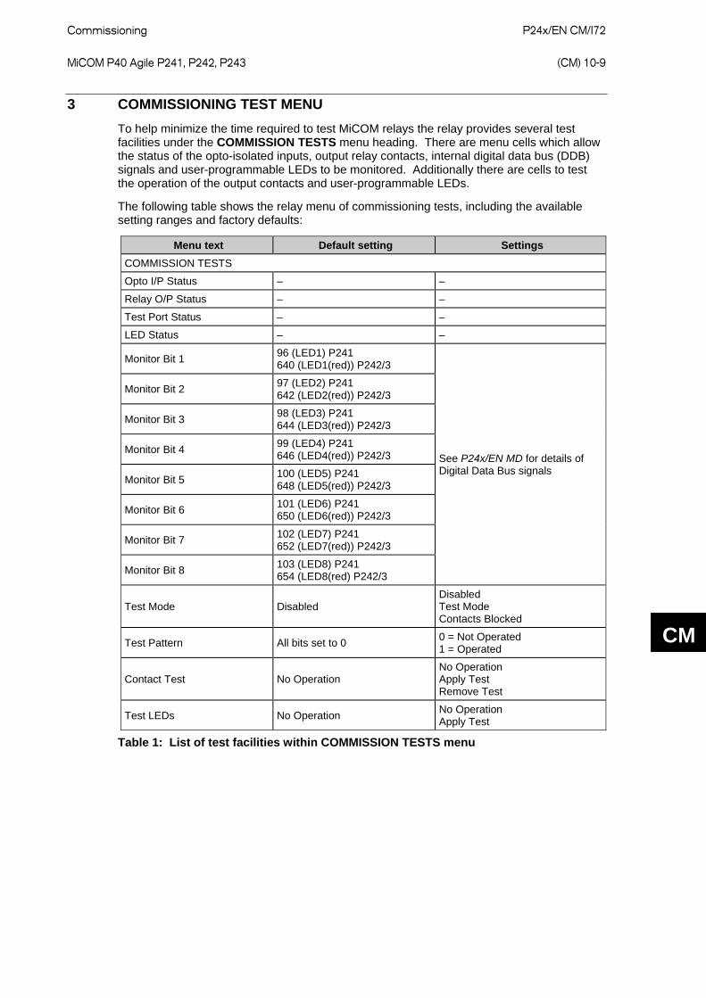
Commissioning
P24x/EN CM/I72 MiCOM P40 Agile P241, P242, P243 (CM) 10-9
CM
3 COMMISSIONING TEST MENU To help minimize the time required to test MiCOM relays the relay provides several test facilities under the COMMISSION TESTS menu heading. There are menu cells which allow the status of the opto-isolated inputs, output relay contacts, internal digital data bus (DDB) signals and user-programmable LEDs to be monitored. Additionally there are cells to test the operation of the output contacts and user-programmable LEDs.
The following table shows the relay menu of commissioning tests, including the available setting ranges and factory defaults:
Menu text Default setting Settings COMMISSION TESTS
Opto I/P Status – –
Relay O/P Status – –
Test Port Status – –
LED Status – –
Monitor Bit 1 96 (LED1) P241 640 (LED1(red)) P242/3
See P24x/EN MD for details of Digital Data Bus signals
Monitor Bit 2 97 (LED2) P241 642 (LED2(red)) P242/3
Monitor Bit 3 98 (LED3) P241 644 (LED3(red)) P242/3
Monitor Bit 4 99 (LED4) P241 646 (LED4(red)) P242/3
Monitor Bit 5 100 (LED5) P241 648 (LED5(red)) P242/3
Monitor Bit 6 101 (LED6) P241 650 (LED6(red)) P242/3
Monitor Bit 7 102 (LED7) P241 652 (LED7(red)) P242/3
Monitor Bit 8 103 (LED8) P241 654 (LED8(red) P242/3
Test Mode Disabled Disabled Test Mode Contacts Blocked
Test Pattern All bits set to 0 0 = Not Operated 1 = Operated
Contact Test No Operation No Operation Apply Test Remove Test
Test LEDs No Operation No Operation Apply Test
Table 1: List of test facilities within COMMISSION TESTS menu
P24x/EN CM/I72
Commissioning (CM) 10-10 MiCOM P40 Agile P241, P242, P243
CM
3.1 Opto I/P status This menu cell displays the status of the relays opto-isolated inputs as a binary string, a 1 indicating an energized opto-isolated input and a 0 a de-energized one. If the cursor is moved along the binary numbers the corresponding label text is displayed for each logic input.
It can be used during commissioning or routine testing to monitor the status of the opto-isolated inputs while they are sequentially energized with a suitable dc voltage.
3.2 Relay O/P status This menu cell displays the status of the digital data bus (DDB) signals that result in energization of the output relays as a binary string, a 1 indicating an operated state and 0 a non-operated state. If the cursor is moved along the binary numbers the corresponding label text is displayed for each relay output.
The information displayed can be used during commissioning or routine testing to indicate the status of the output relays when the relay is ‘in service’. Additionally fault finding for output relay damage can be performed by comparing the status of the output contact under investigation with its associated bit.
Note: When the Test Mode cell is set to Enabled this cell continues to indicate which contacts would operate if the relay was in-service, it does not show the actual status of the output relays.
3.3 Test port status This menu cell displays the status of the eight digital data bus (DDB) signals that have been allocated in the Monitor Bit cells. If the cursor is moved along the binary numbers the corresponding DDB signal text string is displayed for each monitor bit.
By using this cell with suitable monitor bit settings, the state of the DDB signals can be displayed as various operating conditions or sequences are applied to the relay. Therefore the programmable scheme logic can be tested.
Alternatively, the optional monitor/download port test box can be plugged into the monitor/download port located behind the bottom access cover. Details of the monitor/download port test box can be found in section 3.10 of this chapter.
3.4 LED status The LED Status cell is an eight bit binary string that indicates which of the user-programmable LEDs on the relay are illuminated when accessing the relay from a remote location, a 1 indicating a particular LED is lit and a 0 not lit.
3.5 Monitor bits 1 to 8 The eight Monitor Bit cells allow the user to select the status of which digital data bus signals can be observed in the Test Port Status cell or using the monitor or download port.
Each Monitor Bit is set by entering the required digital data bus (DDB) signal number (0 - 1022) from the list of available DDB signals. The pins of the monitor or download port used for monitor bits are given in the table below. The signal ground is available on pins 18, 19, 22 and 25.
Monitor bit 1 2 3 4 5 6 7 8
Monitor/download port pin 11 12 15 13 20 21 23 24
The monitor/download port does not have electrical isolation against
induced voltages on the communications channel. It should only be used for local communications.
Commissioning
P24x/EN CM/I72 MiCOM P40 Agile P241, P242, P243 (CM) 10-11
CM
3.6 Test mode The Test Mode menu cell is used to allow secondary injection testing to be performed on the relay without operation of the trip contacts. The Test Mode is also used in the IEC 60870-5-103 protocol, see section 5.8 of P24x/EN SC. It also enables a facility to directly test the output contacts by applying menu controlled test signals. To select test mode the Test Mode menu cell should be set to Test Mode which takes the relay out of service and blocks the maintenance counters. It also causes an alarm condition to be recorded and the yellow Out of Service LED to illuminate and an alarm message Prot’n. Disabled is given. To enable testing of output contacts the Test Mode cell should be set to Contacts Blocked. This blocks the protection from operating the contacts and enables the test pattern and contact test functions which can be used to manually operate the output contacts. Once testing is complete the cell must be set back to Disabled to restore the relay back to service.
When the ‘test mode’ cell is set to contacts blocked’ the relay scheme logic does not drive the output relays. Therefore, the protection will not trip the associated circuit breaker if a fault occurs.
3.7 Test pattern The Test Pattern cell is used to select the output relay contacts that are tested when the Contact Test cell is set to Apply Test. The cell has a binary string with one bit for each user-configurable output contact which can be set to 1 to operate the output under test conditions and 0 to not operate it.
3.8 Contact test When the Apply Test command in this cell is issued the contacts set for operation (set to 1) in the Test Pattern cell change state. After the test has been applied the command text on the LCD changes to No Operation and the contacts remain in the Test State until reset issuing the Remove Test command. The command text on the LCD reverts to No Operation after the Remove Test command has been issued.
Note: When the Test Mode cell is set to Enabled the Relay O/P Status cell does not show the current status of the output relays and so can not be used to confirm operation of the output relays. Therefore it is necessary to monitor the state of each contact in turn.
3.9 Test LEDs When the Apply Test command in this cell is issued the eight user-programmable LEDs switch ON for approximately 2 seconds before they Switch OFF and the command text on the LCD changes to No Operation.
3.10 Red LED status and green LED status (P242/3) The Red LED Status and Green LED Status cells are eighteen bit binary strings that show which of the user-programmable LEDs on the relay are switched ON when accessing the relay from a remote location, a 1 indicating a particular LED is lit and a 0 not lit. When the status of a particular LED in both cells is 1, this means the LEDs is yellow.
3.11 Using a monitor/download port test box A monitor/download port test box containing 8 LED’s and a switchable audible indicator is available from General Electric, or one of their regional sales offices. It is housed in a small plastic box with a 25-pin male D-connector that plugs directly into the relay’s monitor/download port. There is also a 25-pin female D-connector which allows other connections to be made to the monitor/download port while the monitor/download port test box is in place.
Each LED corresponds to one of the monitor bit pins on the monitor/download port with Monitor Bit 1 being on the left hand side when viewing from the front of the relay. The audible indicator can either be selected to sound if a voltage appears any of the eight monitor pins or remain silent so that indication of state is by LED alone.
P24x/EN CM/I72
Commissioning (CM) 10-12 MiCOM P40 Agile P241, P242, P243
CM
4 EQUIPMENT REQUIRED FOR COMMISSIONING
4.1 Minimum equipment required Overcurrent test set with interval timer
110 V ac voltage supply (if stage 1 of the overcurrent function is set directional)
Multimeter with suitable ac current range, and ac and dc voltage ranges of 0 - 440 V and
0 - 250 V respectively
Continuity tester (if not included in multimeter)
Phase angle meter
Phase rotation meter
100 Ω precision wire wound or metal film resistor, 0.1% tolerance (0°C±2°C)
Note: Modern test equipment may contain many of the above features in one unit.
4.2 Optional equipment Multi-finger test plug type MMLB01 or P992 (if test block type MMLG or P991 installed).
An electronic or brushless insulation tester with a dc output not exceeding 500 V (For insulation resistance testing when required).
A portable PC, with appropriate software (This enables the rear communications port to be tested if this is to be used and saves considerable time during commissioning).
KITZ K-Bus to EIA(RS)232 protocol converter (if first rear EIA(RS)485 K-Bus port or second rear port configured for K-Bus is being tested and one is not already installed).
EIA(RS)485 to EIA(RS)232 converter (if first rear EIA(RS)485 port or second rear port configured for EIA(RS)485 is being tested).
A printer (for printing a setting record from the portable PC).
Commissioning
P24x/EN CM/I72 MiCOM P40 Agile P241, P242, P243 (CM) 10-13
CM
5 PRODUCT CHECKS These product checks cover all aspects of the relay that need to be checked to ensure that it has not been physically damaged prior to commissioning, is functioning correctly and all input quantity measurements are within the stated tolerances.
If the application-specific settings have been applied to the relay prior to commissioning, it is advisable to make a copy of the settings so as to allow their restoration later. If programmable scheme logic other than the default settings with which the relay is supplied have been applied the default settings should be restored prior to commissioning. This could be done by:
• Obtaining a setting file on a diskette from the customer. (This requires a portable PC with appropriate setting software for transferring the settings from the PC to the relay).
• Extracting the settings from the relay itself. (This again requires a portable PC with appropriate setting software).
• Manually creating a setting record. This could be done using a copy of the setting record located at the end of this sub-document to record the settings as the relay’s menu is sequentially stepped through via the front panel user interface.
If password protection is enabled and the customer has changed password 2 that prevents unauthorized changes to some of the settings, either the revised password 2 should be provided, or the customer should restore the original password prior to commencement of testing.
Note: If the password is lost, a recovery password can be obtained from General Electric by quoting the serial number of the relay. The recovery password is unique to that relay and is unlikely to work on any other relay.
Before carrying out any work on the equipment the user should be familiar with the contents of the Safety Section/Safety Guide Pxxx-SG-4LM-2 or later issue and the ratings on the equipment’s rating label.
5.1 With the relay re-energized The following group of tests should be carried out without the auxiliary supply being applied to the relay and with the trip circuit isolated.
The current and voltage transformer connections must be isolated from the relay for these checks. If a P991 or MMLG test block is provided, the required isolation can easily be achieved by inserting test plug type P992 or MMLB01 which effectively open-circuits all wiring routed through the test block.
Before inserting the test plug, check the scheme (wiring) diagram to make sure it does not potentially cause damage or a safety hazard. For example, the test block may be associated with protection current transformer circuits. It is essential that the sockets in the test plug which correspond to the current transformer secondary windings are linked before the test plug is inserted into the test block.
DANGER: Never open circuit the secondary circuit of a current transformer since the high voltage produced may be lethal and could damage insulation.
If a test block is not provided, the voltage transformer supply to the relay should be isolated by using the panel links or connecting blocks. The line current transformers should be short-circuited and disconnected from the relay terminals. Where means of isolating the auxiliary supply and trip circuit (isolation links, fuses and MCB) are provided, these should be used. If this is not possible, the wiring to these circuits needs to be disconnected and the exposed ends suitably terminated to prevent them from being a safety hazard.
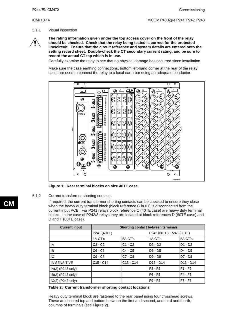
P24x/EN CM/I72
Commissioning (CM) 10-14 MiCOM P40 Agile P241, P242, P243
CM
5.1.1 Visual inspection
The rating information given under the top access cover on the front of the relay should be checked. Check that the relay being tested is correct for the protected line/circuit. Ensure that the circuit reference and system details are entered onto the setting record sheet. Double-check the CT secondary current rating, and be sure to record the actual CT tap which is in use. Carefully examine the relay to see that no physical damage has occurred since installation.
Make sure the case earthing connections, bottom left-hand corner at the rear of the relay case, are used to connect the relay to a local earth bar using an adequate conductor.
Figure 1: Rear terminal blocks on size 40TE case
5.1.2 Current transformer shorting contacts If required, the current transformer shorting contacts can be checked to ensure they close when the heavy duty terminal block (block reference C in 01) is disconnected from the current input PCB. For P241 relays block reference C (40TE case) are heavy duty terminal blocks. In the case of P242/3 relays they are located at block references D (60TE case) and D and F (80TE case).
Current input Shorting contact between terminals P241 (40TE) P242 (60TE), P243 (80TE)
1A CT’s 5A CT’s 1A CT’s 5A CT’s
ΙA C3 - C2 C1 - C2 D3 - D2 D1 - D2
ΙB C6 - C5 C4 - C5 D6 - D5 D4 - D5
ΙC C9 - C8 C7 - C8 D9 - D8 D7 - D8
ΙN SENSITIVE C15 - C14 C13 - C14 D15 - D14 D13 - D14
ΙA(2) (P243 only) F3 - F2 F1 - F2
ΙB(2) (P243 only) F6 - F5 F4 - F5
ΙC(2) (P243 only) F9 - F8 F7 - F8
Table 2: Current transformer shorting contact locations
Heavy duty terminal block are fastened to the rear panel using four crosshead screws. These are located top and bottom between the first and second, and third and fourth, columns of terminals (see Figure 2).
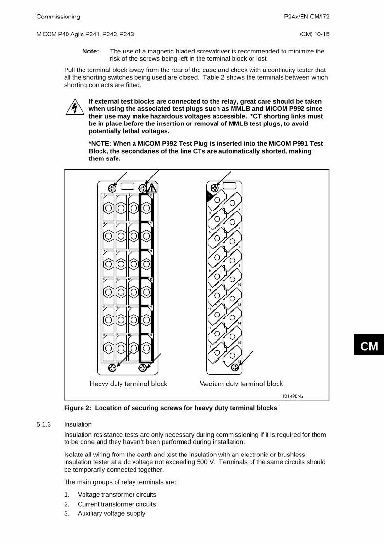
Commissioning
P24x/EN CM/I72 MiCOM P40 Agile P241, P242, P243 (CM) 10-15
CM
Note: The use of a magnetic bladed screwdriver is recommended to minimize the risk of the screws being left in the terminal block or lost.
Pull the terminal block away from the rear of the case and check with a continuity tester that all the shorting switches being used are closed. Table 2 shows the terminals between which shorting contacts are fitted.
If external test blocks are connected to the relay, great care should be taken when using the associated test plugs such as MMLB and MiCOM P992 since their use may make hazardous voltages accessible. *CT shorting links must be in place before the insertion or removal of MMLB test plugs, to avoid potentially lethal voltages.
*NOTE: When a MiCOM P992 Test Plug is inserted into the MiCOM P991 Test Block, the secondaries of the line CTs are automatically shorted, making them safe.
Figure 2: Location of securing screws for heavy duty terminal blocks
5.1.3 Insulation Insulation resistance tests are only necessary during commissioning if it is required for them to be done and they haven’t been performed during installation.
Isolate all wiring from the earth and test the insulation with an electronic or brushless insulation tester at a dc voltage not exceeding 500 V. Terminals of the same circuits should be temporarily connected together.
The main groups of relay terminals are:
1. Voltage transformer circuits 2. Current transformer circuits 3. Auxiliary voltage supply
P24x/EN CM/I72
Commissioning (CM) 10-16 MiCOM P40 Agile P241, P242, P243
CM
4. Field voltage output and opto-isolated control inputs 5. Relay contacts 6. First rear EIA(RS)485 communication port 7. RTD inputs 8. Current loop (analog) inputs and outputs (CLIO) 9. Case earth The insulation resistance should be greater than 100 MΩ at 500 V.
On completion of the insulation resistance tests, ensure all external wiring is correctly reconnected to the unit.
5.1.4 External wiring Check that the external wiring is correct to the relevant relay diagram or scheme diagram. The relay diagram number appears on the rating label under the top access cover on the front of the relay. The corresponding connection diagram is supplied with the General Electric order acknowledgement for the relay.
If a P991 or MMLG test block is provided, the connections should be checked against the scheme (wiring) diagram. It is recommended that the supply connections are to the live side of the test block (colored orange with the odd numbered terminals (1, 3, 5, 7 etc.)). The auxiliary supply is normally routed via terminals 13 (supply positive) and 15 (supply negative), with terminals 14 and 16 connected to the relay’s positive and negative auxiliary supply terminals respectively. However, check the wiring against the schematic diagram for the installation to ensure compliance with the customer’s normal practice.
5.1.5 Watchdog contacts Using a continuity tester, check that the watchdog contacts are in the states given in Table 3 for a de-energized relay.
Terminals Contact state Relay de-energized Relay energized F11 - F12 J11 - J12 M11 - M12
(P241 40TE) (P242 60TE) (P243 80TE)
Closed Open
F13 - F14 J13 - J14 M13 - M14
(P241 40TE) (P242 60TE) (P243 80TE)
Open Closed
Table 3: Watchdog contact status
5.1.6 Auxiliary supply The relay can be operated from either a dc only or an ac/dc auxiliary supply depending on the relay’s nominal supply rating. The incoming voltage must be within the operating range specified in Table 4.
Without energizing the relay, measure the auxiliary supply to ensure it is within the operating range.
Nominal supply rating DC [AC rms] DC operating range AC operating range
24 - 48 V [-] 19 - 65 V -
48 - 110 V [30 - 100 V] 37 - 150 V 24 - 110 V
110 - 240 V [100 - 240 V] 87 - 300 V 80 - 265 V
Table 4: Operational range of auxiliary supply Vx
Note: The relay can withstand an ac ripple of up to 12% of the upper rated voltage on the dc auxiliary supply.

Commissioning
P24x/EN CM/I72 MiCOM P40 Agile P241, P242, P243 (CM) 10-17
CM
Do not energize the relay using the battery charger with the battery disconnected as this can irreparably damage the relay’s power supply circuitry.
Energize the relay only if the auxiliary supply is within the operating range. If test block is provided, it may be necessary to link across the front of the test plug to connect the auxiliary supply to the relay.
5.2 With the relay energized The following group of tests verify that the relay hardware and software is functioning correctly and should be carried out with the auxiliary supply applied to the relay.
The current and voltage transformer connections must remain isolated from the relay for these checks. The trip circuit should also remain isolated to prevent accidental operation of the associated circuit breaker.
5.2.1 Watchdog contacts Using a continuity tester, check the watchdog contacts are in the states given in Table 2 for an energized relay.
5.2.2 LCD front panel display The liquid crystal display is designed to operate in a wide range of substation ambient temperatures. For this purpose, the Px40 relays have an LCD Contrast setting. This allows the user to adjust how light or dark the characters are displayed. The contrast is factory pre-set to account for a standard room temperature, however it may be necessary to adjust the contrast to give the best in-service display. To change the contrast, cell [09FF: LCD Contrast] at the bottom of the CONFIGURATION column can be incremented (darker) or decremented (lighter), as required.
Care: Before applying a contrast setting, make sure the display is not too light or dark so that the menu text becomes unreadable. To restore a visible display download the MiCOM S1 Studio setting file, with the LCD Contrast set in the typical range of 7 - 11.
5.2.3 Date and time Before setting the date and time, ensure that the factory-fitted battery isolation strip that prevents battery drain during transportation and storage has been removed. With the lower access cover open, presence of the battery isolation strip can be checked by a red tab protruding from the positive side of the battery compartment. Lightly pressing the battery to prevent it falling out of the battery compartment, pull the red tab to remove the isolation strip.
The data and time should now be set to the correct values. The method of setting depends on whether accuracy is being maintained via the optional inter-range instrumentation group standard B (IRIG-B) port on the rear of the relay.
5.2.3.1 With an IRIG-B signal If a satellite time clock signal conforming to IRIG-B is provided and the relay has the optional IRIG-B port fitted, the satellite clock equipment should be energized.
To allow the relays time and date to be maintained from an external IRIG-B source cell [0804: DATE and TIME, IRIG-B Sync.] must be set to Enabled.
Ensure the relay is receiving the IRIG-B signal by checking that cell [0805: DATE and TIME, IRIG-B Status] reads Active.
Once the IRIG-B signal is active, adjust the time offset of the universal co-ordinated time (satellite clock time) on the satellite clock equipment so that local time is displayed.
P24x/EN CM/I72
Commissioning (CM) 10-18 MiCOM P40 Agile P241, P242, P243
CM
Check the time, date and month are correct in cell [0801: DATE and TIME, Date/Time]. The IRIG-B signal does not contain the current year so it needs to be set manually in this cell.
If the auxiliary supply fails, with a battery fitted in the compartment behind the bottom access cover, the time and date is maintained. Therefore, when the auxiliary supply is restored, the time and date are correct and not need to be set again.
To test this, remove the IRIG-B signal, then remove the auxiliary supply from the relay. Leave the relay de-energized for approximately 30 seconds. On re-energization, the time in cell [0801: DATE and TIME, Date/Time] should be correct.
Reconnect the IRIG-B signal.
5.2.3.2 Without an IRIG-B signal If the time and date is not being maintained by an IRIG-B signal, ensure that cell [0804: DATE and TIME, IRIG-B Sync.] is set to Disabled.
Set the date and time to the correct local time and date using cell [0801: DATE and TIME, Date/Time].
If the auxiliary supply fails, with a battery fitted in the compartment behind the bottom access cover, the time and date is maintained. Therefore when the auxiliary supply is restored the time and date are correct and not need to be set again.
To test this, remove the auxiliary supply from the relay for approximately 30 seconds. On re-energization, the time in cell [0801: DATE and TIME, Date/Time] should be correct.
5.2.4 Light emitting diodes (LEDs) On power up the green LED should have switch on and stay on indicating that the relay is healthy. The relay has non-volatile memory which remembers the state (on or off) of the alarm, trip and, if configured to latch, user-programmable LED indicators when the relay was last energized from an auxiliary supply. Therefore these indicators may also switch on when the auxiliary supply is applied.
If any of these LEDs are on, then they should be reset before proceeding with further testing. If the LED’s successfully reset (the LED goes out), there is no testing required for that LED because it is known to be operational.
5.2.4.1 Testing the alarm and out of service LEDs The alarm and out of service LEDs can be tested using the COMMISSIONING TESTS menu column. Set cell [0F0D: COMMISSIONING TESTS, Test Mode] to Contacts Blocked. Check that the out of service LED illuminates continuously and the alarm LED flashes.
It is not necessary to return cell [0F0D: COMMISSIONING TESTS, Test Mode] to Disabled at this stage because the test mode will be required for later tests.
5.2.4.2 Testing the trip LED The trip LED can be tested by initiating a manual circuit breaker trip from the relay. However, the trip LED operates during the setting checks performed later. Therefore no further testing of the trip LED is required at this stage.
5.2.4.3 Testing the user-programmable LEDs To test the user-programmable LEDs set cell [0F10: COMMISSIONING TESTS, Test LEDs] to Apply Test. Check that all 8 (P241) or 18 (P242/3) programmable LEDs on the relay illuminate.
5.2.5 Field voltage supply The relay generates a field voltage of nominally 48 V that can be used to energize the opto-isolated inputs (alternatively the substation battery may be used).
Measure the field voltage across terminals 7 and 9 on the terminal block given in Table 5. Check that the field voltage is within the range 40 V to 60 V when no load is connected and that the polarity is correct.
Commissioning
P24x/EN CM/I72 MiCOM P40 Agile P241, P242, P243 (CM) 10-19
CM
Repeat for terminals 8 and 10.
Supply rail Terminals P241 (40TE) P242 (60TE) P243 (80TE)
+ve F7 & F8 J7 & J8 M7 & M8
-ve F9 & F10 J9 & J10 M9 & M10
Table 5: Field voltage terminals
5.2.6 Input opto-isolators This test checks that all the opto-isolated inputs are functioning correctly. The P241 relay has 8 opto-isolated inputs in the 40TE case. The P242 relay has 16 opto-isolated inputs in the 60TE case and the P243 has 16 opto-isolated inputs in the 80TE case.
Energize the opto-isolated inputs one at a time, see the Installation chapter (P24x/EN IN) for the terminal numbers. Ensure that the correct opto input nominal voltage is set in the Opto Config. Menu. Ensure correct polarity and connect the field supply voltage to the appropriate terminals for the input being tested. Each opto input also has selectable filtering. This allows use of a pre-set filter of ½ cycle that renders the input immune to induced noise on the wiring.
Note: The opto-isolated inputs may be energized from an external dc auxiliary supply (such as the station battery) in some installations. Check that this is not the case before connecting the field voltage otherwise damage to the relay may result. If an external 24/27 V, 30/34 V, 48/54 V, 110/125 V, 220/250 V supply is being used it will be connected to the relay's optically isolated inputs directly. If an external supply is being used then it must be energized for this test but only if it has been confirmed that it is suitably rated with less than 12% ac ripple.
The status of each opto-isolated input can be viewed using either cell [0020: SYSTEM DATA, Opto Ι/P Status] or [0F01: COMMISSIONING TESTS, Opto Ι/P Status], a 1 indicating an energized input and a 0 indicating a de-energized input. When each opto-isolated input is energized one of the characters on the bottom line of the display changes to indicate the new state of the inputs.
5.2.7 Output relays This test checks that all the output relays are functioning correctly. The P241 relay has 7 output relays in the 40TE case. The P242 relay has 16 output relays in the 60TE case and the P243 has 16 output relays in the 80TE case.
Ensure that the cell [0F0D: COMMISSIONING TESTS, Test Mode] is set to Contacts Blocked.
The output relays should be energized one at a time. To select output relay 1 for testing, set cell [0F0E: COMMISSIONING TESTS, Test Pattern] 00000000000000000000000000000001.
Connect a continuity tester across the terminals corresponding to output relay 1 as given in the external connection diagram (P24x/EN IN).
To operate the output relay, set cell [0F0F: COMMISSIONING TESTS, Contact Test] to Apply Test. Operation is confirmed by the continuity tester operating for a normally open contact and ceasing to operate for a normally closed contact. Measure the resistance of the contacts in the closed state.
Reset the output relay by setting cell [0F0F: COMMISSIONING TESTS, Contact Test] to Remove Test.
Note: Make sure that thermal ratings of anything connected to the output relays during the contact test procedure is not exceeded by the associated output relay being operated for too long. It is therefore advised that the time between application and removal of contact test is kept to the minimum.
P24x/EN CM/I72
Commissioning (CM) 10-20 MiCOM P40 Agile P241, P242, P243
CM
Repeat the test for the rest of the relays.
Return the relay to service by setting cell [0F0D: COMMISSIONING TESTS, Test Mode] to Disabled.
5.2.8 RTD inputs This test checks that all the RTD inputs are functioning correctly and is only performed on relays with the RTD board fitted.
A 100 Ω resistor, preferably with a tolerance of 0.1%, should be connected across each RTD in turn for PT100 and Ni100 RTDs and a 120 Ω resistor for Ni120 RTDs. The resistor needs to have a very small tolerance as RTDs complying to BS EN 60751: 1995 typically have a change of resistance of 0.39 Ω per °C, therefore the use of a precision wire wound or metal film resistor is recommended. It is essential to connect the RTD common return terminal to the appropriate RTD input otherwise the relay reports an RTD error as it assumes that the RTD wiring has been damaged. The connections required for testing each RTD input are given in Table 6.
Check that the corresponding temperature displayed in the MEASUREMENTS 3 column of the menu is 0°C ±2°C. This range takes into account the 0.1% resistor tolerance and relay accuracy of ±1°C. If a resistor of lower accuracy is used during testing the acceptable setting range needs to be increased.
RTD Terminal connections Measurement cell
(in ‘measurements 3’ column (04) of menu)
Resistor between Wire between
1 B1 and B2 B2 and B3 [0405: RTD 1 Label]
2 B4 and B5 B5 and B6 [0406: RTD 2 Label]
3 B7 and B8 B8 and B9 [0407: RTD 3 Label]
4 B10 and B11 B11 and B12 [0408: RTD 4 Label]
5 B13 and B14 B14 and B15 [0409: RTD 5 Label]
6 B16 and B17 B17 and B18 [040A: RTD 6 Label]
7 B19 and B20 B20 and B21 [040B: RTD 7 Label]
8 B22 and B23 B23 and B24 [040C: RTD 8 Label]
9 B25 and B26 B26 and B27 [040D: RTD 9 Label]
10 B28 and B29 B29 and B30 [040E: RTD 10 Label]
Table 6: RTD input terminals
5.2.9 Current loop inputs This test checks that all the current loop (analog) inputs are functioning correctly and is only performed on relays with the CLIO (current loop input output) board fitted.
Relay terminal connections can be found by referring to the connection diagrams in the Installation chapter, P24x/EN IN.
Note: The current loop inputs the physical connection of the 0 - 1 mA input is different from that of the 0 - 10, 0 - 20 and 4 - 20 mA inputs, as shown in the connection diagrams.
An accurate dc current source can be used to apply various current levels to the current loop inputs. Another approach is to use the current loop output as a convenient and flexible dc current source to test the input protection functionality. Externally the current loop outputs can be fed into their corresponding current loop inputs. Then by applying a certain level of analog signal, such as VA, to the relay the required dc output level can be obtained from the current loop output which is feeding the current loop input.

Commissioning
P24x/EN CM/I72 MiCOM P40 Agile P241, P242, P243 (CM) 10-21
CM
Enable the current loop input to be tested. Set the CLIx minimum and maximum settings and the CLIx Input type for the application.
Apply a dc current to the relay current loop input at 50% of the CLI input maximum range, 0.5 mA (0 - 1 mA CLI), 5 mA (0 - 10 mA CLI) or 10 mA (0 - 20, 4 - 20 mA CLI).
Check the accuracy of the current loop input using the MEASUREMENTS 3 - ANALOG Input 1/2/3/4 column of the menu. The display should show (CLIx maximum + CLIx minimum)/2 1% full scale accuracy.
5.2.10 Current loop (analog) outputs This test checks that all the current loop (analog) outputs are functioning correctly and is only performed on relays with the CLIO board fitted.
Relay terminal connections can be found by referring to the connection diagrams in P24x/EN IN.
Note: For the current loop outputs the physical connection of the 0 - 1 mA output is different from that of the 0 - 10, 0 - 20 and 4 - 20 mA outputs, as shown in the connection diagrams.
Enable the current loop output to be tested. Set the Analog Output parameter, Analog Outputx minimum and maximum settings and the Analogx Output type (range) for the application. Apply the appropriate analog input parameter to the relay equals to (Analogx maximum + Analogx minimum)/2. The current loop output should be at 50% of its maximum rated output. Using a precision resistive current shunt together with a high-resolution voltmeter, check that the analog (current loop) output is at 50% of its maximum rated output, 0.5 mA (0 - 1 mA CLO), 5 mA (0 - 10 mA CLO) or 10 mA (0 - 20, 4 – 20 mA CLO). The accuracy should be within ±0.5% of full scale + meter accuracy.
5.2.11 First rear communications port This test should only be performed where the relay is to be accessed from a remote location and varies depending on the communications standard being adopted.
It is not the intention of the test to verify the operation of the complete system from the relay to the remote location, just the relay’s rear communications port and any protocol converter necessary.
5.2.11.1 Courier communications If a K-Bus to EIA(RS)232 KITZ protocol converter is installed, connect a portable PC running the appropriate software (such as MiCOM S1 Studio or PAS&T) to the incoming (remote from relay) side of the protocol converter.
If a KITZ protocol converter is not installed, it may not be possible to connect the PC to the relay installed. In this case a KITZ protocol converter and portable PC running appropriate software should be temporarily connected to the relay’s first rear K-Bus port. The terminal numbers for the relays first rear K-Bus port are given in Table 7. However, as the installed protocol converter is not being used in the test, only the correct operation of the relays
K-Bus port will be confirmed.
Connection Terminal K-Bus MODBUS or VDEW P241 (40TE) P242 (60TE) P243 (80TE)
Screen Screen F16 J16 M16
1 +ve F17 J17 M17
2 -ve F18 J18 M18
Table 7: EIA(RS)485 terminals
Ensure that the communications baud rate and parity settings in the application software are set the same as those on the protocol converter (usually a KITZ but could be a SCADA RTU). The relays Courier address in cell [0E02: COMMUNICATIONS, Remote Address] must be set to a value between 1 and 254.
P24x/EN CM/I72
Commissioning (CM) 10-22 MiCOM P40 Agile P241, P242, P243
CM
Check that communications can be established with this relay using the portable PC.
If the relay has the optional fiber optic communications port fitted, the port to be used should be selected by setting cell [0E07: COMMUNICATIONS, Physical Link] to Fiber Optic. Ensure that the relay address and baud rate settings in the application software are set the same as those in cell [0E04 COMMUNICATIONS, Baud Rate] of the relay. Check that, using the Master Station, communications with the relay can be established.
5.2.11.2 MODBUS communications Connect a portable PC running the appropriate MODBUS Master Station software to the relay’s first rear EIA(RS)485 port via an EIA(RS)485 to EIA(RS)232 interface converter. The terminal numbers for the relay’s EIA(RS)485 port are given in Table 6.
Ensure that the relay address, baud rate and parity settings in the application software are set the same as those in cells [0E02: COMMUNICATIONS, Remote Address], [0E04: COMMUNICATIONS, Baud Rate] and [0E05: COMMUNICATIONS, Parity] of the relay.
Check that communications with this relay can be established.
If the relay has the optional fiber optic communications port fitted, the port to be used should be selected by setting cell [0E07: COMMUNICATIONS, Physical Link] to Fiber Optic. Ensure that the relay address and baud rate settings in the application software are set the same as those in cell [0E04: COMMUNICATIONS, Baud Rate] of the relay. Check that, using the Master Station, communications with the relay can be established.
5.2.11.3 IEC 60870-5-103 (VDEW) communications If the relay has the optional fiber optic communications port fitted, the port to be used should be selected by setting cell [0E07: COMMUNICATIONS, Physical Link] to Fiber Optic or EIA(RS)485.
IEC 60870-5-103/VDEW communication systems are designed to have a local Master Station and this should be used to verify that the relay’s rear fiber optic or EIA(RS)485 port, as appropriate, is working.
Ensure that the relay address and baud rate settings in the application software are set the same as those in cells [0E02: COMMUNICATIONS, Remote Address] and [0E04: COMMUNICATIONS, Baud Rate] of the relay.
Check that, using the Master Station, communications with the relay can be established.
5.2.11.4 IEC 61850 communications Connect a portable PC running the appropriate IEC 61850 Master Station Software or MMS browser to the relays Ethernet port (RJ45 or ST fiber optic connection). The terminal numbers for the relays Ethernet port are given in Table 8.
Configuration of the relay IP parameters (IP Address, Subnet Mask, Gateway) and SNTP time synchronization parameters (SNTP Server 1, SNTP Server 2) is performed by the IED Configurator tool. If these parameters are not available from an SCL file, they must be configured manually.
If the assigned IP address is duplicated elsewhere on the same network, the remote communications operates in an indeterminate way. However, the relay checks for a conflict on every IP configuration change and at power up. An alarm is raised if an IP conflict is detected. The relay can be configured to accept data from networks other than the local network by using the Gateway setting.
Check that communications with this relay can be established.
To communicate with an IEC 61850 IED on Ethernet, it is necessary only to know its IP address. This can then be configured into either:
• An IEC 61850 client (or master), for example a PACiS computer (MiCOM C264) or HMI, or
• An MMS browser, with which the full data model can be retrieved from the IED, without any prior knowledge
Commissioning
P24x/EN CM/I72 MiCOM P40 Agile P241, P242, P243 (CM) 10-23
CM
Setting changes such as protection settings are not supported in the current IEC 61850 implementation. Such setting changes are done using MiCOM S1 Studio using the front port serial connection of the relay, or over the Ethernet link if preferred. This is known as tunneling. See SCADA Communications chapter, P24x/EN SC for more information on IEC 61850.
The connector for the Ethernet port is a shielded RJ-45. The table below shows the signals and pins on the connector.
Pin Signal name Signal definition 1 TXP Transmit (positive)
2 TXN Transmit (negative)
3 RXP Receive (positive)
4 - Not used
5 - Not used
6 RXN Receive (negative)
7 - Not used
8 - Not used
Table 8: Signals on the Ethernet connector
5.2.12 Second rear communications port This test should only be performed where the relay is to be accessed from a remote location and varies depending on the communications standard being adopted.
It is not the intention of the test to verify the operation of the complete system from the relay to the remote location, just the relays rear communications port and any protocol converter necessary.
5.2.12.1 K-Bus configuration If a K-Bus to EIA(RS)232 KITZ protocol converter is installed, connect a portable PC running the appropriate software (MiCOM S1 Studio or PAS&T) to the incoming (remote from relay) side of the protocol converter.
If a KITZ protocol converter is not installed, it may not be possible to connect the PC to the relay installed. In this case a KITZ protocol converter and portable PC running appropriate software should be temporarily connected to the relay’s second rear communications port configured for K-Bus. The terminal numbers for the relay’s K-Bus port are given in Table 9. However, as the installed protocol converter is not being used in the test, only the correct operation of the relay’s K-Bus port is confirmed.
Pin* Connection 4 EIA(RS)485 - 1 (+ ve)
7 EIA(RS)485 - 2 (- ve)
Table 9: Second rear communications port K-Bus terminals
* - All other pins unconnected.
Ensure that the communications baud rate and parity settings in the application software are set the same as those on the protocol converter (usually a KITZ but could be a SCADA RTU). The relay’s Courier address in cell [0E90: COMMUNICATIONS, RP2 Address] must be set to a value between 1 and 254. The second rear communication’s port configuration [0E88: COMMUNICATIONS RP2 Port Config.] must be set to K-Bus.
Check that communications can be established with this relay using the portable PC.
P24x/EN CM/I72
Commissioning (CM) 10-24 MiCOM P40 Agile P241, P242, P243
CM
5.2.12.2 EIA(RS)485 configuration If an EIA(RS)485 to EIA(RS)232 converter (CK222) is installed, connect a portable PC running the appropriate software (MiCOM S1 Studio) to the EIA(RS)232 side of the converter and the second rear communications port of the relay to the EIA(RS)485 side of the converter.
The terminal numbers for the relay’s EIA(RS)485 port are given in Table 6.
Ensure that the communications baud rate and parity settings in the application software are set the same as those in the relay. The relays Courier address in cell [0E90: COMMUNICATIONS, RP2 Address] must be set to a value between 1 and 254. The second rear communication’s port configuration [0E88: COMMUNICATIONS RP2 Port Config.] must be set to EIA(RS)485.
Check that communications can be established with this relay using the portable PC.
5.2.12.3 EIA(RS)232 configuration Connect a portable PC running the appropriate software (MiCOM S1 Studio) to the rear EIA(RS)2321 port of the relay.
The second rear communications port connects via the 9-way female D-type connector (SK4). The connection is compliant to EIA(RS)574.
Pin Connection 1 No Connection
2 RxD
3 TxD
4 DTR#
5 Ground
6 No Connection
7 RTS#
8 CTS#
9 No Connection
Table 10: Second rear communications port EIA(RS)232 terminals
# - These pins are control lines for use with a modem.
Connections to the second rear port configured for EIA(RS)232 operation can be made using a screened multi-core communication cable up to 15 m long, or a total capacitance of 2500 pF. The cable should be terminated at the relay end with a 9-way, metal shelled, D-type male plug. The terminal numbers for the relay’s EIA(RS)232 port are given in Table 8.
Ensure that the communications baud rate and parity settings in the application software are set the same as those in the relay. The relays Courier address in cell [0E90: COMMUNICATIONS, RP2 Address] must be set to a value between 1 and 254. The second rear communication’s port configuration [0E88: COMMUNICATIONS RP2 Port Config] must be set to EIA(RS)232.
Check that communications can be established with this relay using the portable PC.
5.2.13 Current inputs This test verifies that the accuracy of current measurement is within the acceptable tolerances.
All relays leave the factory set for operation at a system frequency of 50 Hz. If operation at 60 Hz is required, this must be set in cell [0009: SYSTEM DATA, Frequency].
Apply current equal to the line current transformer secondary winding rating to each current transformer input of the corresponding rating in turn, checking its magnitude using a
1 This port is actually compliant to EIA(RS)574; the 9-pin version of EIA(RS)232, see www.tiaonline.org.
Commissioning
P24x/EN CM/I72 MiCOM P40 Agile P241, P242, P243 (CM) 10-25
CM
multimeter. Refer to Table 11 for the corresponding reading in the relays MEASUREMENTS 1 or MEASUREMENTS 3 columns, as appropriate, and record the value displayed.
Menu cell Apply current to
P241 (40TE) P242 (60TE) P243 (80TE)
1 A CTs 5 A CTs 1 A CTs 5 A CTs [0201: MEASUREMENTS 1, ΙA Magnitude] C3 - C2 C1 - C2 D3 - D2 D1 - D2
[0203: MEASUREMENTS 1, ΙB Magnitude] C6 - C5 C4 - C5 D6 - D5 D4 - D5
[0205: MEASUREMENTS 1, ΙC Magnitude] C9 - C8 C7 - C8 D9 - D8 D7 - D8
[020B: MEASUREMENTS 1, ΙSEF Magnitude] C15 - C14 C13 - C14 D15 - D14 D13 - D14
[0230: MEASUREMENTS 1, ΙA-2 Magnitude] (P243 only) F3 - F2 F1 - F2
[0232: MEASUREMENTS 1, ΙB-2 Magnitude] (P243 only) F6 - F5 F4 - F5
[0234: MEASUREMENTS 1, ΙC-2 Magnitude] (P243 only) F9 - F8 F7 - F8
Table 11: Current input terminals
The measured current values displayed on the relay LCD or a portable PC connected to the front communication port, are either be in primary or secondary Amperes. If cell [0D02: MEASURE’T SETUP, Local Values] is set to Primary, the values displayed should be equal to the applied current multiplied by the corresponding current transformer ratio set in the CT and VT RATIOS menu column (see Table 12). If cell [0D02: MEASURE’T SETUP, Local Values] is set to Secondary, the value displayed should be equal to the applied current.
Note: If a PC connected to the relay’s rear communications port is used to display the measured current, the process is similar. However, the setting of cell [0D03: MEASURE’T SETUP, Remote Values] determines whether the displayed values are in primary or secondary Amperes.
The measurement accuracy of the relay is ±1%. However, an additional allowance must be made for the accuracy of the test equipment being used.
Menu cell Corresponding CT ratio
(in ‘VT and CT RATIO column (0A) of menu)
[0201: MEASUREMENTS 1, ΙA Magnitude]
[0203: MEASUREMENTS 1, ΙB Magnitude]
[0205: MEASUREMENTS 1, ΙC Magnitude]
[0230: MEASUREMENTS 1, ΙA - 2 Magnitude] (P243 only) [0232: MEASUREMENTS 1, ΙB - 2 Magnitude] (P243 only) [0234: MEASUREMENTS 1, ΙC - 2 Magnitude] (P243 only)
[0A07: Phase CT Primary] [0A08: Phase CT Sec'y]
[020B: MEASUREMENTS 1, ΙSEF Magnitude] [0A0B: SEF CT Primary] [0A0C: SEF CT Sec’y]
Table 12: CT ratio settings
P24x/EN CM/I72
Commissioning (CM) 10-26 MiCOM P40 Agile P241, P242, P243
CM
5.2.14 Voltage inputs This test verifies the accuracy of voltage measurement is within the acceptable tolerances.
Three modes of connection are available on the P24x relay: either 3VTs connection, or 2VTs plus residual VT connection or 2VTs plus remanent voltage VT connection (see Installation Chapter, P24x/EN IN for detailed information).
The following tests will be realized with the VT Connecting Mode set to 3 VT which is the most used configuration.
Apply rated voltage to each voltage transformer input in turn, checking its magnitude using a multimeter. Refer to Table 13 for the corresponding reading in the relays MEASUREMENTS 1 column and record the value displayed.
Menu cell Voltage applied to
P241 (40TE) P242 (60TE), P243 (80TE)
[021A: MEASUREMENTS 1, VAN Magnitude] C19 - C22 D19 - D22
[021C: MEASUREMENTS 1, VBN Magnitude] C20 - C22 D20 - D22
[021E: MEASUREMENTS 1, VCN Magnitude] C21 - C22 D21 - D22
[0220: MEASUREMENTS 1, VN Measured Mag] C23 - C24 D23 - D24
Table 13: Voltage input terminals
The measured voltage values displayed on the relay LCD or a portable PC connected to the front communication port will either be in primary or secondary volts. If cell [0D02: MEASURE’T SETUP, Local Values] is set to Primary, the values displayed should be equal to the applied voltage multiplied by the corresponding voltage transformer ratio set in the VT and CT RATIOS menu column (see Table 14). If cell [0D02: MEASURE’T SETUP, Local Values] is set to Secondary, the value displayed should be equal to the applied voltage.
Note: If a PC connected to the relay’s rear communications port is used to display the measured voltage, the process is similar. However, the setting of cell [0D03: MEASURE’T SETUP, Remote Values] determines whether the displayed values are in primary or secondary volts.
The measurement accuracy of the relay is ±1%. However, an additional allowance must be made for the accuracy of the test equipment being used.
Menu cell Corresponding VT ratio
(in ‘VT and CT RATIO column (0A) of menu)
[021A: MEASUREMENTS 1, VAN Magnitude] [021C: MEASUREMENTS 1, VBN Magnitude] [021E: MEASUREMENTS 1, VCN Magnitude]
[0A01: Main VT Primary] [0A02: Main VT Sec’y]
Table 14: VT ratio settings
Commissioning
P24x/EN CM/I72 MiCOM P40 Agile P241, P242, P243 (CM) 10-27
CM
6 SETTING CHECKS The setting checks ensure that all of the application-specific relay settings (that is both the relays function and programmable scheme logic settings) for the particular installation have been correctly applied to the relay.
If the application-specific settings are not available, ignore sections 6.1 and 6.2
Note: The trip circuit should remain isolated during these checks to prevent accidental operation of the associated circuit breaker.
6.1 Apply application-specific settings There are two methods of applying the settings:
• Transferring them from a pre-prepared setting file to the relay using a portable PC running the appropriate software (MiCOM S1 Studio) using the relays front EIA(RS)232 port, located under the bottom access cover, or the first rear communications port (Courier protocol with a KITZ protocol converter connected), or the second rear communications port. This method is preferred for transferring function settings as it is much faster and there is less margin for error. If programmable scheme logic other than the default settings with which the relay is supplied is to be used then this is the only way of changing the settings.
• If a setting file has been created for the particular application and provided on a diskette, the commissioning time is further reduced, especially if application-specific programmable scheme logic is applied to the relay.
• Enter the settings manually using the relay’s operator interface. This method is not suitable for changing the programmable scheme logic.
When the installation needs application-specific Programmable Scheme Logic it is essential that the appropriate .psl file is downloaded (sent) to the relay, for each and every setting group that will be used. If the user fails to download the required .psl file to any setting group that may be brought into service, the factory default PSL will still be resident. This may have severe operational and safety consequences.
6.2 Check application-specific settings The settings applied should be carefully checked against the required application-specific settings to ensure they have been entered correctly. However, this is not considered essential if a customer-prepared setting file on diskette has been transferred to the relay using a portable PC.
There are two methods of checking the settings:
• Extract the settings from the relay using a portable PC running the appropriate software (MiCOM S1 Studio) using the front EIA(RS)232 port, located under the bottom access cover, or the first rear communications port (Courier protocol with a KITZ protocol converter connected), or the second rear communications port. Compare the settings transferred from the relay with the original written application-specific setting record. (For cases where the customer has only provided a printed copy of the required settings but a portable PC is available).
• Step through the settings using the relays operator interface and compare them with the original application-specific setting record.
Unless previously agreed, the application-specific programmable scheme logic is not checked as part of the commissioning tests.
Due to the versatility and possible complexity of the programmable scheme logic, it is beyond the scope of these commissioning instructions to detail suitable test procedures. Therefore, when programmable scheme logic tests must be performed, written tests which will satisfactorily demonstrate the correct operation of the application-specific scheme logic should be devised by the Engineer who created it. These should be provided to the Commissioning Engineer together with the diskette containing the programmable scheme logic setting file.
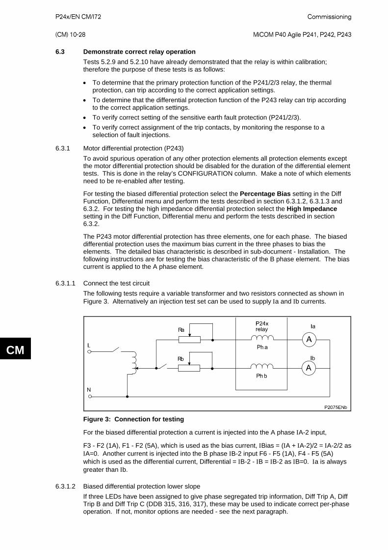
P24x/EN CM/I72
Commissioning (CM) 10-28 MiCOM P40 Agile P241, P242, P243
CM
6.3 Demonstrate correct relay operation Tests 5.2.9 and 5.2.10 have already demonstrated that the relay is within calibration; therefore the purpose of these tests is as follows:
• To determine that the primary protection function of the P241/2/3 relay, the thermal protection, can trip according to the correct application settings.
• To determine that the differential protection function of the P243 relay can trip according to the correct application settings.
• To verify correct setting of the sensitive earth fault protection (P241/2/3). • To verify correct assignment of the trip contacts, by monitoring the response to a
selection of fault injections.
6.3.1 Motor differential protection (P243) To avoid spurious operation of any other protection elements all protection elements except the motor differential protection should be disabled for the duration of the differential element tests. This is done in the relay’s CONFIGURATION column. Make a note of which elements need to be re-enabled after testing.
For testing the biased differential protection select the Percentage Bias setting in the Diff Function, Differential menu and perform the tests described in section 6.3.1.2, 6.3.1.3 and 6.3.2. For testing the high impedance differential protection select the High Impedance setting in the Diff Function, Differential menu and perform the tests described in section 6.3.2.
The P243 motor differential protection has three elements, one for each phase. The biased differential protection uses the maximum bias current in the three phases to bias the elements. The detailed bias characteristic is described in sub-document - Installation. The following instructions are for testing the bias characteristic of the B phase element. The bias current is applied to the A phase element.
6.3.1.1 Connect the test circuit The following tests require a variable transformer and two resistors connected as shown in Figure 3. Alternatively an injection test set can be used to supply Ιa and Ιb currents.
Figure 3: Connection for testing
For the biased differential protection a current is injected into the A phase ΙA-2 input,
F3 - F2 (1A), F1 - F2 (5A), which is used as the bias current, ΙBias = (ΙA + ΙA-2)/2 = ΙA-2/2 as ΙA=0. Another current is injected into the B phase ΙB-2 input F6 - F5 (1A), F4 - F5 (5A) which is used as the differential current, Differential = ΙB-2 - ΙB = ΙB-2 as ΙB=0. Ιa is always greater than Ιb.
6.3.1.2 Biased differential protection lower slope If three LEDs have been assigned to give phase segregated trip information, Diff Trip A, Diff Trip B and Diff Trip C (DDB 315, 316, 317), these may be used to indicate correct per-phase operation. If not, monitor options are needed - see the next paragraph.
Commissioning
P24x/EN CM/I72 MiCOM P40 Agile P241, P242, P243 (CM) 10-29
CM
Go to the COMMISSION TESTS column in the menu, scroll down and change cells [0F05: Monitor Bit 1] to 315, [0F06: Monitor Bit 2] to 316 and [0F07: Monitor Bit 3] to 317. Cell [0F04: Test Port Status] will now appropriately set or reset the bits that now represent Phase A Trip (DDB 315), Phase B Trip (DDB 316) and Phase C Trip (DDB 317) with the rightmost bit representing Phase A Trip. From now on you should monitor the indication of [0F04: Test Port Status].
Adjust the variac and the resistor to inject 1 pu into ΙA-2 to give a bias current of 0.5 pu in the A-phase.
Note: 1 pu = 1 A into terminals, F3 - F2 for 1 A applications; or 1 pu = 5 A into terminals F1-F2 for 5 A applications.
The relay trips and any contacts associated with the A-phase operates, and bit 1 (rightmost) of [0F04: Test Port Status] are set to 1. Some LEDs, including the yellow alarm LED, will come on, but ignore them for the moment.
Slowly increase the current in the B-phase ΙB-2 input F6 - F5 (1A), F4 - F5 (5 A) until phase B trips (Bit 2 of [0F04: Test Port Status] is set to 1). Record the phase B current magnitude and check that it corresponds to the information below. Switch OFF the ac supply and reset the alarms.
Bias current (ΙA-2/2) Differential current (ΙB) Phase Magnitude Phase Magnitude
A 0.5 pu B 0.05 pu +/-10%
Assumption: Ιs1 = 0.05 pu, k1 = 0%, Ιs2 = 1.2 pu
For other differential settings the formula below can be used (enter k1 slope in pu form, for example percentage/100):
B phase operate current is (Ιs1 + ΙBias x k1) pu +/- 10%
6.3.1.3 Biased differential protection upper slope Repeat the test in 6.3.1.2 with the A phase, IA-2, current set to be 3.4 pu (Ibias = 1.7 pu).
Slowly increase the current in the B phase until phase B trips (bit 2 of [0F04: Test Port Status] is set to 1). Record the phase B current magnitude and check that it corresponds to the information below.
Switch OFF the ac supply and reset the alarms.
Bias current (ΙA-2/2) Differential current (ΙB) Phase Magnitude Phase Magnitude
A 1.7 pu B 0.8 pu +/-20%
Assumption: Ιs1 = 0.05 pu, k1 = 0%, Ιs2 = 1.2 pu, k2 =150%as above
For other differential settings the formula below can be used (enter k1 and k2 slopes in pu form, for example percentage/100):
Operate current is [(ΙBias x k2) + (k1 – k2) x Ιs2 + Ιs1] pu +/- 20%
Note: Particularly for 5 A applications the duration of current injections should be short to avoid overheating of the variac or injection test set.
6.3.2 Motor differential operation and contact assignment
6.3.2.1 Phase A Retaining the same test circuit as before, prepare for an instantaneous injection of 4 x Ιs1 pu current in the A phase, with no current in the B phase (B phase switch open). Connect a timer to start when the fault injection is applied, and to stop when the trip occurs.
P24x/EN CM/I72
Commissioning (CM) 10-30 MiCOM P40 Agile P241, P242, P243
CM
Determine which output relay has been selected to operate when a Diff. Trip occurs by viewing the relay’s programmable scheme logic. The programmable scheme logic can only be changed using the appropriate software. If this software is not available then the default output relay allocations are still applicable. In the default PSL, relay 3 is the designated protection trip contact and DDB 371 Any Trip is assigned to this contact.
Ensure that the timer is reset.
Apply a current of 4 x the setting in cell [3002: GROUP 1 DIFFERENTIAL, Diff Is1] to the relay and note the time displayed when the timer stops.
After applying the test check the red trip led and yellow alarm led turns on when the relay operates. Check ‘Alarms/Faults Present - Tripped Phase A, Diff Trip’ is on the display. Reset the alarms.
Three Pole Tripping DDB 318 Diff Trip
Single Pole Tripping DDB 315: Diff Trip A
DDB 316: Diff Trip B
DDB 317: Diff Trip C
6.3.2.2 Phase B Reconfigure the test equipment to inject fault current into the B phase. Repeat the test in 6.3.2.1, this time ensuring that the breaker trip contacts relative to B phase operation close correctly. Record the phase B trip time. Check the red trip led and yellow alarm led turns on when the relay operates. Check ‘Alarms/Faults Present - Tripped Phase B, Diff Trip’ is on the display. Reset the alarms.
6.3.2.3 Phase C Repeat 6.3.2.2 for the C phase.
The average of the recorded operating times for the three phases should be less than 30 ms. Switch OFF the ac supply and reset the alarms.
On completion of the tests any protection elements which were disabled for testing purposes must have their original settings restored in the CONFIGURATION column.
6.3.3 Sensitive earth fault protection This test, performed on stage 1 of the sensitive earth fault protection function in setting Group 1, demonstrates that the relay is operating correctly at the application-specific settings.
It is not considered necessary to check the boundaries of operation where cell [3202: SENSITIVE E/F GROUP 1, ISEF>1 Direction] is set to Directional Fwd as the test detailed already confirms the correct functionality between current and voltage inputs, processor and outputs and earlier checks confirmed the measurement accuracy is within the stated tolerance.
To avoid spurious operation of any other protection elements all protection elements except the overcurrent protection should be disabled for the duration of the overcurrent element tests. This is done in the relay’s CONFIGURATION column. Make a note of which elements need to be re-enabled after testing.
6.3.3.1 Connect the test circuit Determine which output relay has been selected to operate when a ΙSEF>1 trip occurs by viewing the relay’s programmable scheme logic.
The programmable scheme logic can only be changed using the appropriate software. If this software is not available then the default output relay allocations are still applicable.
If ΙSEF>1 trip (DDB 261) is not mapped directly to an output relay in the programmable scheme logic, output relay 3 should be used for the test as it operates for any trip condition, DDB 371 Any Trip is assigned to this contact.
Commissioning
P24x/EN CM/I72 MiCOM P40 Agile P241, P242, P243 (CM) 10-31
CM
The associated terminal numbers can be found from the external connection diagrams in the Installation chapter, P24x/EN IN.
Connect the output relay so that its operation trips the test set and stops the timer.
Connect the current output of the test set to the ‘ISensitive’ phase current transformer input of the relay (terminals C15 – C14 (1 A, 40TE case), D15 – D14 (1 A, 60TE case), F15 – F14 (1 A, 80TE case), C13 – C14 (5 A, 40TE case), D13 – D14 (5 A, 60TE case) F13 – F14 (5 A, 80TE case)).
Ensure that the timer starts when the current is applied to the relay.
6.3.3.2 Perform the test Ensure that the timer is reset.
Apply a current of twice the setting in cell [3203: GROUP 1 SENSITIVE E/F, SEF>1 Current Set] to the relay and note the time displayed when the timer stops.
Check the red trip led and yellow alarm led turns on when the relay operates. Check ‘Alarms/Faults Present - Started Phase N, Tripped Phase N, Start ISEF>1, Trip ISEF>1’ is on the display. Reset all alarms.
6.3.3.3 Check the operating time Check that the operating time recorded by the timer is within the range shown in Table 15.
Note: Except for the definite time characteristic, the operating times given in Table 14 are for a time multiplier or time dial setting of 1. Therefore, to obtain the operating time at other time multiplier or time dial settings, the time given in Table 14 must be multiplied by the setting of cell [3205: GROUP 1 SENSITIVE E/F, ΙSEF>1 TMS] for IEC and UK characteristics or cell [3207: GROUP 1 SENSITIVE E/F, ΙSEF>1 Time Dial] for IEEE and US characteristics.
In addition, for definite time and inverse characteristics there is an additional delay of up to 0.02 second and 0.08 second respectively that may need to be added to the relays acceptable range of operating times.
For all characteristics, allowance must be made for the accuracy of the test equipment being used.
Characteristic Operating time at twice current setting and time multiplier/time dial setting of 1.0
Nominal (seconds) Range (seconds) DT [3504: ΙSEF>1 T Delay] setting Setting ±5%
IEC S Inverse 10.03 9.53 - 10.53
IEC V Inverse 13.50 12.83 - 14.18
IEC E Inverse 26.67 25.34 - 28
UK LT Inverse 120.00 114.00 - 126.00
IEEE M Inverse 3.8 3.61 - 3.99
IEEE V Inverse 7.03 6.68 - 7.38
IEEE E Inverse 9.52 9.04 - 10
US Inverse 2.16 2.05 - 2.27
US ST Inverse 12.12 11.51 - 12.73
Table 15: Characteristic operating times for Ι>1
On completion of the tests any protection elements that were disabled for testing purposes must have their original settings restored in the CONFIGURATION column.
P24x/EN CM/I72
Commissioning (CM) 10-32 MiCOM P40 Agile P241, P242, P243
CM
6.3.4 Thermal overload protection P24x relays model the time-current thermal characteristic of a motor by internally generating a thermal replica of the machine. The aim of this test is to check:
• The presence of a thermal alarm as soon as the thermal state reaches the set threshold • The time to a thermal trip in case of a thermal overload • The measurements of the thermal load and thermal state The settings of this function are listed in the THERMAL OVERLOAD, GROUP 1 menu column. Check these settings before the test.
To avoid spurious operation of any other protection elements all protection elements except the thermal protection should be disabled for the duration of the thermal element tests. This is done in the relay’s CONFIGURATION column. Make a note of which elements need to be re-enabled after testing.
6.3.4.1 Connect the test circuit Determine which output relay has been selected to operate when a thermal trip occurs by viewing the relays programmable scheme logic.
The programmable scheme logic can only be changed using the appropriate software. If this software is not available then the default output relay allocations are still applicable.
If the Thermal Trip (DDB 236) is not mapped directly to an output relay in the programmable scheme logic, output relay 3 should be used for the test as it operates for any trip condition, DDB 371 Any Trip is assigned to this contact. The Thermal Alarm (DDB 178) should be mapped directly to an output relay in the programmable scheme logic if this feature is to be tested.
The associated terminal numbers can be found from the external connection diagrams in the Installation chapter, P24x/EN IN.
Connect the output relay so that its operation trips the test set and stops the timer.
Connect the current output of the test set to the A phase current transformer input of the relay (terminals C3 – C2 (1 A, 40TE case), D3 – D2 (1 A, 60TE case), F3 – F2 (1 A, 80TE case), C1 – C2 (5 A, 40TE case), D1 – D2 (5 A, 60TE case) F1 – F2 (5 A, 80TE case)).
Ensure that the timer starts when the current is applied to the relay.
Note: If the timer does not start when the current is applied, the connections may be incorrect for the direction of operation set. Try again with the current connections reversed.
6.3.4.2 Perform the test Ensure that the timer on the test set is reset.
Ensure that the thermal state is reset (see in cell [0402: MEASUREMENTS 3, Thermal State]: if not, this reset can be done through the cell [0404: MEASUREMENTS 3, Reset Th State] by selecting YES.
Check the position of the interrupting device by viewing the status of the two opto-inputs (52a and 52b status inputs) used to indicate the device position. The 52a input must be energized to simulate the closed position of the interrupting device to enable the thermal protection heating time constants. The cooling time constant is used when the interrupting device is open.
Apply a current of twice the setting [in cell 3001: THERMAL OVERLOAD, GROUP1, Ith Current Set] to the relay and note the time displayed when the timer stops. If it is required to repeat the test, make sure to disable Thermal Lockout [in cell 3009]. Also make sure to disable the inhibit during start setting Inh Trip Dur St [in cell 300B]. Since most portable secondary injection test sets have limited current output capability, it is suggested to change the Ith Current Set to 1 A (after the as found value is recorded) and use the 1 A phase current input terminals. To save time during testing, it is advisable to set all the thermal time constants to 5 minutes.

Commissioning
P24x/EN CM/I72 MiCOM P40 Agile P241, P242, P243 (CM) 10-33
CM
Ensure that the thermal state is reset to 0 (see cell [0402: MEASUREMENTS 3, ThermalState]. If not, the thermal state can be reset through the cell [0404: MEASUREMENTS 3, Reset Th State] by selecting YES.
On completion of the tests any protection elements that were disabled for testing purposes must have their original settings restored in the CONFIGURATION column.
6.3.4.3 Verify the operating time This test is done by a single-phase injection on the A phase current input, it results in that the relay sees equal current magnitudes for both positive and negative phase sequence quantities. On injection of a single phase current value equal to Iinject, the relay sees current magnitudes of Iinject/3 for both positive and negative phase sequences quantities and Iinject for Irms. The equivalent thermal current value Ieq calculated by the relay is given by the following:
I eq = √(I12 + K I22)
Note: This equation is used in software version A4.x(09) and before
or
I eq = √(Irms2 + K I22)
Note: This equation is used in software version B1.0(20) or later
Where:
I1 = Positive sequence current
Irms: root mean square current
I2: negative sequence current
K is a constant proportional to the thermal capacity of the motor (K Coefficient default setting = 3)
The equivalent motor heating current assuming K = 3 for (1) becomes:
Ieq = √ [ 4 * ( Iinject / 3 ) 2 ]
= ( 2 Iinject / 3 ) (3)
The equivalent motor heating current assuming K = 3 for (2) becomes:
Ieq = √ [ 4/3 * ( Iinject) 2 ]
= ( 2 Iinjected / √3 ) (4)
The equation used to calculate the trip time at 100% of thermal state is:
t = τ ln((k2 – A)/(k2–1)) where the value of τ (thermal time constant) depends on the current value absorbed by the motor:
τ = T1 (Thermal Const T1) if Ith < Ieq< = 2*Ith overload time constant
τ = T2 (Thermal Const T2) if Ieq> 2*Ith start-up time constant
τ = Tr (Cooling Const Tr) if interrupting device is opened cooling time constant
Ith = thermal setting in cell [3001: THERMAL OVERLOAD, GROUP1, Ith Current Set]
k = Ieq / Ith = measured thermal load (or thermal capacity)
A = initial state of the machine, in percentage of the thermal state = 0 for this test.
The time to a thermal trip becomes:

P24x/EN CM/I72
Commissioning (CM) 10-34 MiCOM P40 Agile P241, P242, P243
CM
t = τ ln(k2/(k2–1)) The equation used to calculate the time to the thermal alarm is:
talarm = τ ln(k2/(k2–Thermal Alarm /100)) Thermal alarm = (Thermal Alarm) thermal alarm setting in percentage of the thermal state
Since a current of twice the setting Ith is applied, consequently one of the following thermal constants is used:
• T1 (overload time constant) if the interrupting device is closed. • Tr (cooling time constant) if the interrupting device is opened. Apply a current of twice the setting [in cell 3001: THERMAL OVERLOAD, GROUP1, Ith Current Set] to the relay and note the time displayed when the timer stops. Check that the operating time recorded by the timer is within the range (calculated trip time ±5% or 40 ms whichever is the greater). For all characteristics, allowance must be made for the accuracy of the test equipment being used.
Example
For Ith Current Set = 0.5 A and A phase Iinject = 2 A, T1 = 5 mins
Using (3) k = Ieq / Ith = (2 x 2 /3) / 0.5 = 8/3 A
top = 5 x 60 ln ((8/3)2 / ((8/3)2 – 1)) = 45.465 s
Using (4) k = Ieq / Ith = (2 x 2 /√3) / 0.5 = 8/√3 A
top = 5 x 60 ln ((8/√3) 2 / ((8/√3) 2 – 1)) = 14.4 s
For a thermal alarm setting = 90% using (3) talarm = 40.59 s
For a thermal alarm setting = 90% using (4) talarm = 12.96 s
If the injection is done equally on the 3 phases current transformers, the equation used to evaluate Ieq will be:
I eq = √(I12 + K I22)
Note: This equation is used in software version A4.x(09) and before
or
I eq = √(Irms2 + K I22)
Note: This equation is used in software version B1.0(20) or later
And provided the phase currents are balanced, I2 is zero.
On completion of the tests any protection elements that were disabled for testing purposes must have their original settings restored in the CONFIGURATION column.
Commissioning
P24x/EN CM/I72 MiCOM P40 Agile P241, P242, P243 (CM) 10-35
CM
7 ON-LOAD CHECKS The following on-load measuring checks ensure the external wiring to the current and voltage inputs is correct but can only be carried out if there are no restrictions preventing the energization of the plant being protected.
Remove all test leads, for example temporary shorting leads, and replace any external wiring that has been removed to allow testing.
If you have disconnected any of the external wiring from the relay to perform any of the foregoing tests, you should ensure that all connections are replaced in accordance with the relevant external connection or scheme diagram.
7.1 Voltage connections
Using a multimeter measure the voltage transformer secondary voltages to ensure they are correctly rated. Check that the system phase rotation is correct using a phase rotation meter.
Compare the values of the secondary phase voltages with the relays measured values, which can be found in the MEASUREMENTS 1 menu column.
If cell [0D02: MEASURE’T SETUP, Local Values] is set to Secondary, the values displayed on the relay LCD or a portable PC connected to the front EIA(RS)232 communication port should be equal to the applied secondary voltage. The values should be within 1% of the applied secondary voltages. However, an additional allowance must be made for the accuracy of the test equipment being used.
If cell [0D02: MEASURE’T SETUP, Local Values] is set to Primary, the values displayed should be equal to the applied secondary voltage multiplied the corresponding voltage transformer ratio set in the CT & VT RATIOS menu column (see Table 16). Again the values should be within 1% of the expected value, plus an additional allowance for the accuracy of the test equipment being used.
Voltage Cell in MEASUREMENTS 1 Column (02)
Corresponding VT ratio (in ‘VT and CT RATIO column
(0A) of menu)
VAB [0214: VAB Magnitude] [0A01: Main VT Primary] [0A02: Main VT Sec’y]
VBC [0216: VBC Magnitude]
VCA [0218: VCA Magnitude]
VAN [021A: VAN Magnitude]
VBN [021C: VBN Magnitude]
VCN [021E: VCN Magnitude]
Vremanent [0222: Vr AntiBacks Magnitude]
VN [0220: VN Measured Mag] [0A05: NVD VT Primary] [0A06: NVD VT Sec’y]
Table 16: Measured voltages and VT ratio settings
7.2 Current connections
Measure the current transformer secondary values for each input using a multimeter connected in series with corresponding relay current input.
P24x/EN CM/I72
Commissioning (CM) 10-36 MiCOM P40 Agile P241, P242, P243
CM
Check that the current transformer polarities are correct by measuring the phase angle between the current and voltage, either against a phase meter already installed on site and known to be correct or by determining the direction of power flow by contacting the system control center.
Ensure the current flowing in the neutral circuit of the current transformers is negligible.
Compare the values of the secondary phase currents and phase angle with the relay’s measured values, which can be found in the MEASUREMENTS 1 menu column.
Note: Under normal load conditions the earth fault function measures little, if any, current. It is therefore necessary to simulate a phase to neutral fault. This can be achieved by temporarily disconnecting one or two of the line current transformer connections to the relay and shorting the terminals of these current transformer secondary windings.
Check that the ΙA/ΙB/ΙC Differential currents measured on the P243 relay are less than 10% of the ΙA/ΙB/ΙC Bias currents, see the Measurements 3 menu. Check that the Ι2 Magnitude negative phase sequence current measured by the relay is not greater than expected for the particular installation, see the Measurements 1 menu. Check that the active and reactive power measured by the relay are correct, see the Measurements 2 menu. The power measurement modes are described in the Measurements and Recording chapter, P24x/EN MR.
If cell [0D02: MEASURE’T SETUP, Local Values] is set to Secondary, the currents displayed on the relay LCD or a portable PC connected to the front EIA(RS)232 communication port should be equal to the applied secondary current. The values should be within 1% of the applied secondary currents. However, an additional allowance must be made for the accuracy of the test equipment being used.
If cell [0D02: MEASURE’T SETUP, Local Values] is set to Primary, the currents displayed should be equal to the applied secondary current multiplied by the corresponding current transformer ratio set in CT & VT RATIOS menu column (see Table 16). Again the values should be within 1% of the expected value, plus an additional allowance for the accuracy of the test equipment being used.
Note: If a P241/2/3 relay is applied with a single dedicated current transformer for the earth fault function, it may not be possible to check the relay’s measured values as the neutral current is almost zero.
Commissioning
P24x/EN CM/I72 MiCOM P40 Agile P241, P242, P243 (CM) 10-37
CM
8 FINAL CHECKS The tests are now complete.
Remove all test or temporary shorting leads. If you have disconnected any of the external wiring from the relay to perform
the wiring verification tests, you should ensure that all connections are replaced in accordance with the relevant external connection or scheme diagram.
Ensure that the relay has been restored to service by checking that cell [0F0D: COMMISSIONING TESTS, Test Mode] is set to Disabled.
If the relay is in a new installation or the circuit breaker has just been maintained, the circuit breaker maintenance and current counters should be zero. These counters can be reset using cell [0606: CB CONDITION, Reset All Values]. If the required access level is not active, the relay prompts for a password so that the setting change can be made.
If the menu language was changed to allow accurate testing, it should now be restored to the customer’s preferred language.
If an MMLG test block is installed, remove the MMLB01 test plug and replace the MMLG cover so that the protection is put into service.
Ensure that all event records, fault records, disturbance records, alarms and LEDs have been reset before leaving the relay.
If applicable, replace the secondary front cover on the relay.
P24x/EN CM/I72
Commissioning (CM) 10-38 MiCOM P40 Agile P241, P242, P243
CM
9 COMMISSIONING TEST RECORD
Date: Engineer:
Station: Circuit:
System Frequency: Hz
VT Ratio: / V
CT Ratio (tap in use): / A
Front plate information
Motor protection relay MiCOM P24x
Model number
Serial number
Rated current In 1 A 5 A
Rated voltage Vn
Auxiliary voltage Vx
Test equipment used This section should be completed to allow future identification of protective devices that have been commissioned using equipment that is later found to be defective or incompatible but may not be detected during the commissioning procedure.
Overcurrent test set Model: Serial No:
Phase angle meter Model: Serial No:
Phase rotation meter Model: Serial No:
Insulation tester Model: Serial No:
Setting software: Type: Version:
Have all relevant safety instructions been followed? Yes No 5. PRODUCT CHECKS 5.1 With the relay de-energized 5.1.1 Visual inspection Relay damaged? Yes No Rating information correct for installation? Yes No Case earth installed? Yes No
Commissioning
P24x/EN CM/I72 MiCOM P40 Agile P241, P242, P243 (CM) 10-39
CM
5.1.2 Current transformer shorting contacts close? Yes No Not checked
5.1.3 Insulation resistance >100 MΩ at 500 V dc Yes No Not tested
5.1.4 External wiring Wiring checked against diagram? Yes No
Test block connections checked? Yes No N/A
5.1.5 Watchdog contacts (auxiliary supply off)
Terminals 11 and 12 Contact closed? Contact resistance
Yes No
Ω Not measured
Terminals 13 and 14 Contact open? Yes No
5.1.6 Measured auxiliary supply V ac/dc
5.2 With the relay energized 5.2.1 Watchdog contacts (auxiliary supply on) Terminals 11 and 12 Contact open? Yes No
Terminals 13 and 14 Contact closed? Contact resistance
Yes No
Ω Not measured
5.2.2 LCD front panel display
LCD contrast setting used
5.2.3 Date and time Clock set to local time? Yes No Time maintained when auxiliary supply removed? Yes No 5.2.4 Light emitting diodes Relay healthy (green) LED working? Yes No Alarm (yellow) LED working? Yes No Out of service (yellow) LED working? Yes No Trip (red) LED working? Yes No
All 8 (P241), 18 (P242/3) programmable LEDs working? Yes No
5.2.5 Field supply voltage
Value measured between terminals 7 and 9 V dc
Value measured between terminals 8 and 10 V dc
5.2.6 Input opto-isolators Opto input 1 working? Yes No Opto input 2 working? Yes No Opto input 3 working? Yes No Opto input 4 working? Yes No Opto input 5 working? Yes No Opto input 6 working? Yes No
P24x/EN CM/I72
Commissioning (CM) 10-40 MiCOM P40 Agile P241, P242, P243
CM
Opto input 7 working? Yes No Opto input 8 working? Yes No
Opto input 9 working? Yes No N/A
Opto input 10 working? Yes No N/A
Opto input 11 working? Yes No N/A
Opto input 12 working? Yes No N/A
Opto input 13 working? Yes No N/A
Opto input 14 working? Yes No N/A
Opto input 15 working? Yes No N/A
Opto input 16 working? Yes No N/A
5.2.7 Output relays
Relay 1 working? Contact resistance
Yes No
Ω Not measured
Relay 2 working? Contact resistance
Yes No
Ω Not measured
Relay 3 working? Contact resistance
Yes No
Ω Not measured
Relay 4 working? Contact resistance (N/C) (N/O)
Yes No
Ω Not measured Ω Not measured
Relay 5 working? Contact resistance (N/C) (N/O)
Yes No
Ω Not measured
Ω Not measured
Relay 6 working? Contact resistance (N/C) (N/O)
Yes No
Ω Not measured
Ω Not measured
Relay 7 working? Contact resistance (N/C) (N/O)
Yes No
Ω Not measured
Commissioning
P24x/EN CM/I72 MiCOM P40 Agile P241, P242, P243 (CM) 10-41
CM
Relay 8 working? Contact resistance (N/C) (N/O)
Yes No N/A
Ω Not measured
Ω Not measured
Relay 9 working? Contact resistance
Yes No N/A
Ω Not measured
Ω Not measured
Relay 10 working? Contact resistance
Yes No N/A
Ω Not measured
Relay 11 working? Contact resistance (N/C) (N/O)
Yes No N/A
Ω Not measured
Ω Not measured
Relay 12 working? Contact resistance (N/C) (N/O)
Yes No N/A
Ω Not measured
Ω Not measured
Relay 13 working? Contact resistance (N/C) (N/O)
Yes No N/A
Ω Not measured
Ω Not measured
Relay 14 working? Contact resistance (N/C) (N/O)
Yes No N/A
Ω Not measured
Ω Not measured
Relay 15 working? Contact resistance (N/C) (N/O)
Yes No N/A
Ω Not measured
Ω Not measured
P24x/EN CM/I72
Commissioning (CM) 10-42 MiCOM P40 Agile P241, P242, P243
CM
Relay 16 working? Contact resistance (N/C) (N/O)
Yes No N/A
Ω Not measured
Ω Not measured
5.2.8 RTD inputs Resistor tolerance
RTD 1 reading [04C01: RTD 1 Label] %
RTD 2 reading [04C02: RTD 2 Label] °C
RTD 3 reading [04C03: RTD 3 Label] °C
RTD 4 reading [04C04: RTD 4 Label] °C
RTD 5 reading [04C05: RTD 5 Label] °C
RTD 6 reading [04C06: RTD 6 Label] °C
RTD 7 reading [04C07: RTD 7 Label] °C
RTD 8 reading [04C08: RTD 8 Label] °C
RTD 9 reading [04C09: RTD 9 Label] °C
RTD 10 reading [04C0A: RTD 10 Label] °C
5.2.9 Current loop inputs
Analog input Range
0 - 1 mA 0 - 10 mA 0 - 20 mA 4 - 20 mA
Analog Input 1 reading at 50% maximum range [4D01: CLI1 Input Label]
Analog Input 2 reading at 50% maximum range [4D02: CLI2 Input Label]
Analog Input 3 reading at 50% maximum range [4D03: CLI3 Input Label]
Analog Input 4 reading at 50% maximum range [4D04: CLI4 Input Label]
5.2.10 Current loop outputs
0 - 1 mA 0 - 10 mA 0 - 20 mA 4 - 20 mA
Analog Output Range mA
Analog Output 1 current at 50% of rated output mA
Analog Output 2 current at 50% of rated output mA
Analog Output 3 current at 50% of rated output mA
Analog Output 4 current at 50% of rated output mA
Commissioning
P24x/EN CM/I72 MiCOM P40 Agile P241, P242, P243 (CM) 10-43
CM
5.2.11 First rear communications port
Communication standard
K-Bus MODBUS IEC 60870-5-103 IEC 61850
Communications established? Yes No
Protocol converter tested? Yes No N/A
5.2.12 Second rear communications port K-Bus EIA(RS)485 EIA(RS)232
Communication port configuration Yes No
Communications established? Yes No N/A
Protocol converter tested? 5.2.13 Current inputs
Displayed current Primary Secondary
Phase CT ratio
[Phase CT Primary]
[Phase CT Sec'y] N/A
SEF CT ratio
[SEF CT Primary]
[SEF CT Sec'y] N/A
Input CT Applied Value Displayed Value
ΙA A A
ΙB A A
ΙC A A
ΙN A
N/A A N/A
ISEF A A
ΙA (2) A
N/A A N/A
ΙB (2) A
N/A A N/A
ΙC (2) A
N/A A N/A
5.2.14 Voltage inputs
Displayed voltage Primary Secondary
Main VT ratio
[Main VT Primary]
[Main VT Sec'y.] N/A
NVD VT ratio
[NVD VT Primary]
[NVD VT Secondary] N/A
P24x/EN CM/I72
Commissioning (CM) 10-44 MiCOM P40 Agile P241, P242, P243
CM
Input VT Applied Value Displayed value
Va V V
Vb V V
Vc V V
VN V V
6. SETTING CHECKS 6.1 Application-specific function settings applied? Yes No
Application-specific programmable scheme logic settings applied?
Yes No N/A
6.2 Application-specific function settings verified? Yes No N/A
Application-specific programmable scheme logic tested?
Yes No N/A
6.3 Demonstrate correct relay operation 6.3.1 Motor differential protection (P243)
6.3.1.2 Motor Differential lower slope pickup A
6.3.1.3 Motor Differential upper slope pickup A
6.3.2.1 Motor Differential Phase A contact routing OK? Yes No
Motor Differential Phase A trip time s
6.3.2.2 Motor Differential Phase B contact routing OK? Yes No
Motor Differential Phase B trip time s
6.3.2.3 Motor Differential Phase C contact routing OK? Yes No
Motor Differential Phase C trip time s
Average trip time, Phases A, B and C s
6.3.3 Sensitive E/F protection (P241/P242/P243)
Protection function timing tested? Yes No
SEF type (set in cell [ΙSEF>1 Direction]) Directional Fwd Non-directional
Applied current A
Expected operating time s
Measured operating time s
6.3.4 Thermal Overload protection (P241/P242/P243)
Protection function timing tested? Yes No
Thermal Trip
Applied current A
Expected trip operating time s
Measured trip operating time s
Thermal Alarm
Applied current A
Commissioning
P24x/EN CM/I72 MiCOM P40 Agile P241, P242, P243 (CM) 10-45
CM
Expected alarm operating time s
Measured alarm operating time s
7.1 VT wiring checked? Yes No N/A
Phase rotation correct? Yes No
Displayed voltage Primary Secondary
Main VT ratio
[Main VT Primary]
[Main VT Sec'y.] V N/A
NVD VT ratio
[NVD VT Primary]
[NVD VT Secondary] V N/A
Voltages Applied Value Displayed value
VAN/VAB V V
VBN/VBC V V
VCN/VCA V V
VN V V
7.2 CT wiring checked? Yes No N/A
CT polarities correct? Yes No
Displayed current Primary Secondary
Phase CT ratio
[Phase CT Primary]
[Phase CT Sec'y] A N/A
SEF CT ratio
[SEF CT Primary]
[SEF CT Sec'y] A N/A
Currents Applied Value Displayed value
ΙA A A
ΙB A A
ΙC A A
ΙN A
N/A A N/A
ISEF A A
ΙA (2) P243 only A
N/A A N/A
ΙB (2) P243 only A
N/A A N/A
ΙC (2) P243 only A
N/A A N/A
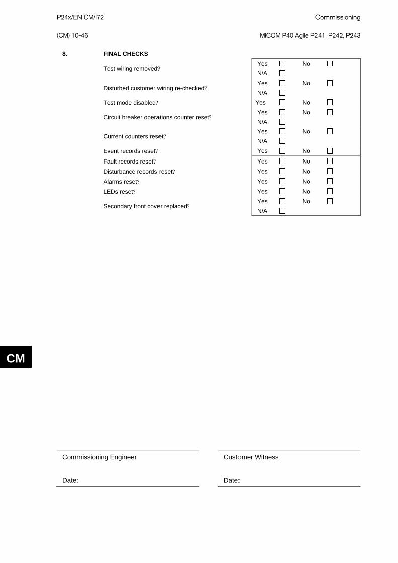
P24x/EN CM/I72
Commissioning (CM) 10-46 MiCOM P40 Agile P241, P242, P243
CM
8. FINAL CHECKS
Test wiring removed? Yes No N/A
Disturbed customer wiring re-checked? Yes No N/A
Test mode disabled? Yes No
Circuit breaker operations counter reset? Yes No N/A
Current counters reset? Yes No N/A
Event records reset? Yes No
Fault records reset? Yes No
Disturbance records reset? Yes No
Alarms reset? Yes No
LEDs reset? Yes No
Secondary front cover replaced? Yes No N/A
Commissioning Engineer Customer Witness
Date: Date:
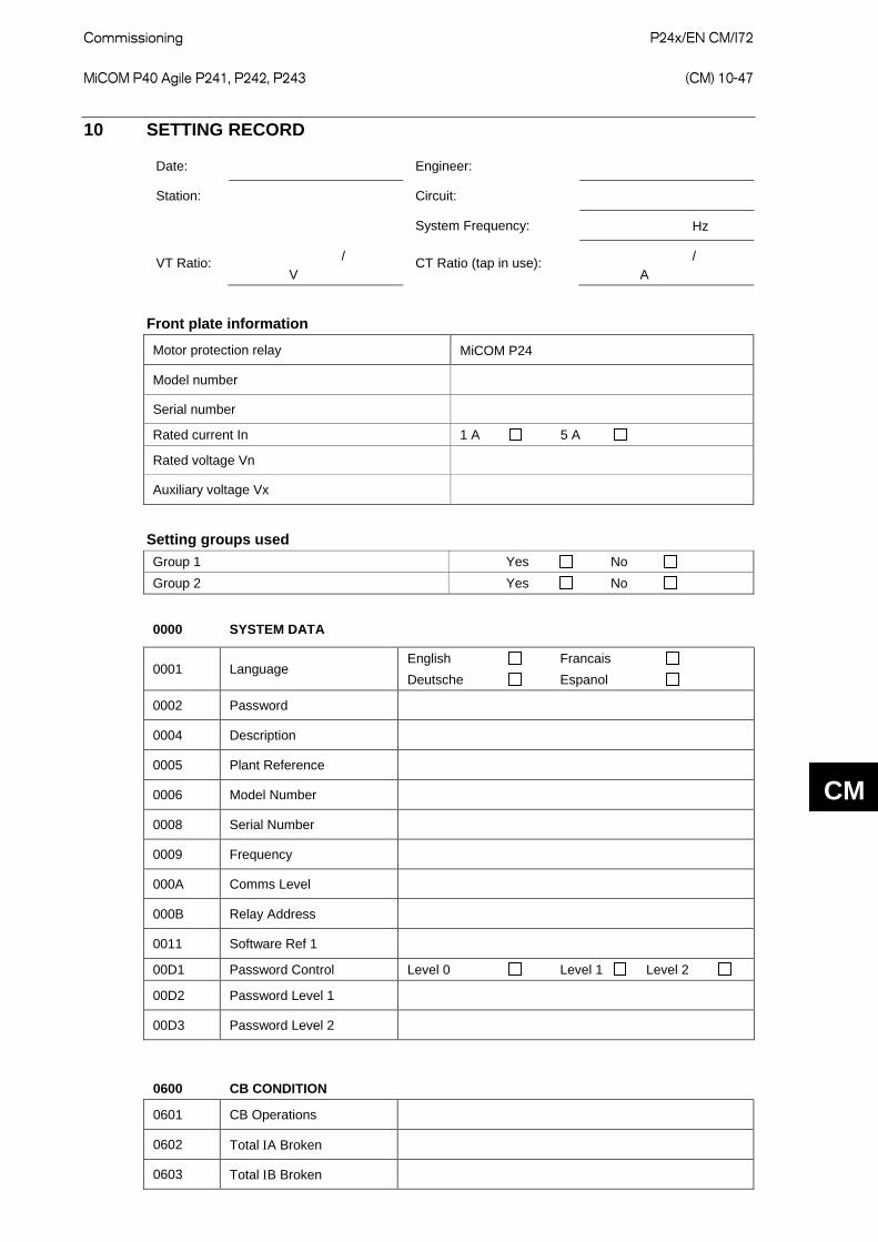
Commissioning
P24x/EN CM/I72 MiCOM P40 Agile P241, P242, P243 (CM) 10-47
CM
10 SETTING RECORD
Date: Engineer:
Station: Circuit:
System Frequency: Hz
VT Ratio: / V
CT Ratio (tap in use): / A
Front plate information
Motor protection relay MiCOM P24
Model number
Serial number
Rated current In 1 A 5 A
Rated voltage Vn
Auxiliary voltage Vx
Setting groups used Group 1 Yes No Group 2 Yes No
0000 SYSTEM DATA
0001 Language English Francais Deutsche Espanol
0002 Password
0004 Description
0005 Plant Reference
0006 Model Number
0008 Serial Number
0009 Frequency
000A Comms Level
000B Relay Address
0011 Software Ref 1
00D1 Password Control Level 0 Level 1 Level 2
00D2 Password Level 1
00D3 Password Level 2
0600 CB CONDITION
0601 CB Operations
0602 Total ΙA Broken
0603 Total ΙB Broken
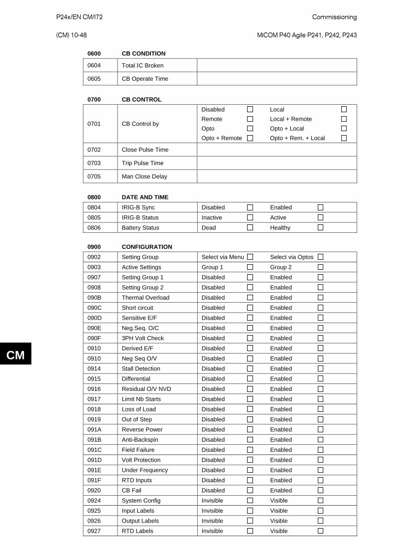
P24x/EN CM/I72
Commissioning (CM) 10-48 MiCOM P40 Agile P241, P242, P243
CM
0600 CB CONDITION
0604 Total ΙC Broken
0605 CB Operate Time
0700 CB CONTROL
0701 CB Control by
Disabled Local Remote Local + Remote Opto Opto + Local Opto + Remote Opto + Rem. + Local
0702 Close Pulse Time
0703 Trip Pulse Time
0705 Man Close Delay
0800 DATE AND TIME 0804 IRIG-B Sync Disabled Enabled
0805 IRIG-B Status Inactive Active
0806 Battery Status Dead Healthy
0900 CONFIGURATION 0902 Setting Group Select via Menu Select via Optos
0903 Active Settings Group 1 Group 2
0907 Setting Group 1 Disabled Enabled
0908 Setting Group 2 Disabled Enabled
090B Thermal Overload Disabled Enabled
090C Short circuit Disabled Enabled
090D Sensitive E/F Disabled Enabled
090E Neg.Seq. O/C Disabled Enabled
090F 3PH Volt Check Disabled Enabled
0910 Derived E/F Disabled Enabled
0910 Neg Seq O/V Disabled Enabled
0914 Stall Detection Disabled Enabled
0915 Differential Disabled Enabled
0916 Residual O/V NVD Disabled Enabled
0917 Limit Nb Starts Disabled Enabled
0918 Loss of Load Disabled Enabled
0919 Out of Step Disabled Enabled
091A Reverse Power Disabled Enabled
091B Anti-Backspin Disabled Enabled
091C Field Failure Disabled Enabled
091D Volt Protection Disabled Enabled
091E Under Frequency Disabled Enabled
091F RTD Inputs Disabled Enabled
0920 CB Fail Disabled Enabled
0924 System Config Invisible Visible
0925 Input Labels Invisible Visible
0926 Output Labels Invisible Visible
0927 RTD Labels Invisible Visible
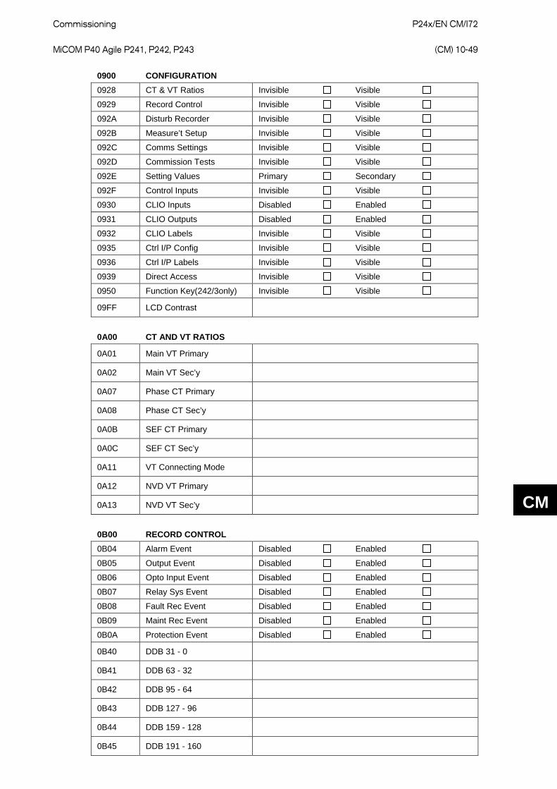
Commissioning
P24x/EN CM/I72 MiCOM P40 Agile P241, P242, P243 (CM) 10-49
CM
0900 CONFIGURATION 0928 CT & VT Ratios Invisible Visible
0929 Record Control Invisible Visible
092A Disturb Recorder Invisible Visible
092B Measure’t Setup Invisible Visible
092C Comms Settings Invisible Visible
092D Commission Tests Invisible Visible
092E Setting Values Primary Secondary
092F Control Inputs Invisible Visible
0930 CLIO Inputs Disabled Enabled
0931 CLIO Outputs Disabled Enabled
0932 CLIO Labels Invisible Visible
0935 Ctrl I/P Config Invisible Visible
0936 Ctrl I/P Labels Invisible Visible
0939 Direct Access Invisible Visible
0950 Function Key(242/3only) Invisible Visible
09FF LCD Contrast
0A00 CT AND VT RATIOS
0A01 Main VT Primary
0A02 Main VT Sec’y
0A07 Phase CT Primary
0A08 Phase CT Sec’y
0A0B SEF CT Primary
0A0C SEF CT Sec’y
0A11 VT Connecting Mode
0A12 NVD VT Primary
0A13 NVD VT Sec’y
0B00 RECORD CONTROL 0B04 Alarm Event Disabled Enabled
0B05 Output Event Disabled Enabled
0B06 Opto Input Event Disabled Enabled
0B07 Relay Sys Event Disabled Enabled
0B08 Fault Rec Event Disabled Enabled
0B09 Maint Rec Event Disabled Enabled
0B0A Protection Event Disabled Enabled
0B40 DDB 31 - 0
0B41 DDB 63 - 32
0B42 DDB 95 - 64
0B43 DDB 127 - 96
0B44 DDB 159 - 128
0B45 DDB 191 - 160
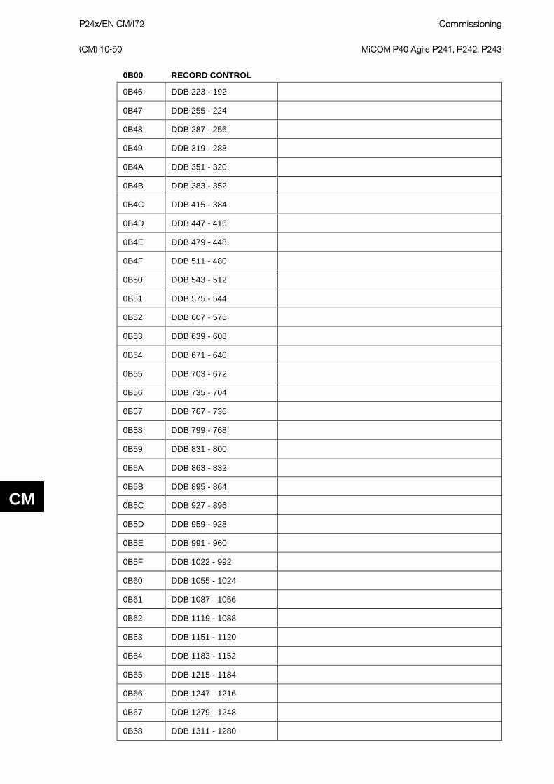
P24x/EN CM/I72
Commissioning (CM) 10-50 MiCOM P40 Agile P241, P242, P243
CM
0B00 RECORD CONTROL
0B46 DDB 223 - 192
0B47 DDB 255 - 224
0B48 DDB 287 - 256
0B49 DDB 319 - 288
0B4A DDB 351 - 320
0B4B DDB 383 - 352
0B4C DDB 415 - 384
0B4D DDB 447 - 416
0B4E DDB 479 - 448
0B4F DDB 511 - 480
0B50 DDB 543 - 512
0B51 DDB 575 - 544
0B52 DDB 607 - 576
0B53 DDB 639 - 608
0B54 DDB 671 - 640
0B55 DDB 703 - 672
0B56 DDB 735 - 704
0B57 DDB 767 - 736
0B58 DDB 799 - 768
0B59 DDB 831 - 800
0B5A DDB 863 - 832
0B5B DDB 895 - 864
0B5C DDB 927 - 896
0B5D DDB 959 - 928
0B5E DDB 991 - 960
0B5F DDB 1022 - 992
0B60 DDB 1055 - 1024
0B61 DDB 1087 - 1056
0B62 DDB 1119 - 1088
0B63 DDB 1151 - 1120
0B64 DDB 1183 - 1152
0B65 DDB 1215 - 1184
0B66 DDB 1247 - 1216
0B67 DDB 1279 - 1248
0B68 DDB 1311 - 1280
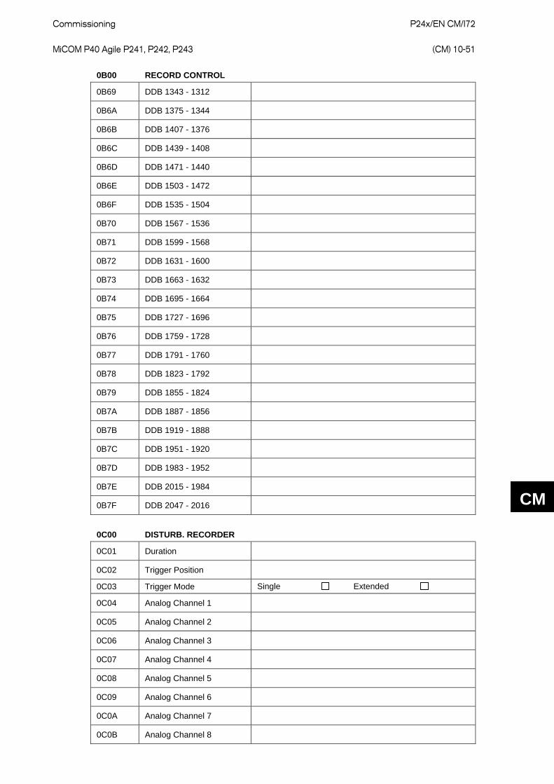
Commissioning
P24x/EN CM/I72 MiCOM P40 Agile P241, P242, P243 (CM) 10-51
CM
0B00 RECORD CONTROL
0B69 DDB 1343 - 1312
0B6A DDB 1375 - 1344
0B6B DDB 1407 - 1376
0B6C DDB 1439 - 1408
0B6D DDB 1471 - 1440
0B6E DDB 1503 - 1472
0B6F DDB 1535 - 1504
0B70 DDB 1567 - 1536
0B71 DDB 1599 - 1568
0B72 DDB 1631 - 1600
0B73 DDB 1663 - 1632
0B74 DDB 1695 - 1664
0B75 DDB 1727 - 1696
0B76 DDB 1759 - 1728
0B77 DDB 1791 - 1760
0B78 DDB 1823 - 1792
0B79 DDB 1855 - 1824
0B7A DDB 1887 - 1856
0B7B DDB 1919 - 1888
0B7C DDB 1951 - 1920
0B7D DDB 1983 - 1952
0B7E DDB 2015 - 1984
0B7F DDB 2047 - 2016
0C00 DISTURB. RECORDER
0C01 Duration
0C02 Trigger Position
0C03 Trigger Mode Single Extended
0C04 Analog Channel 1
0C05 Analog Channel 2
0C06 Analog Channel 3
0C07 Analog Channel 4
0C08 Analog Channel 5
0C09 Analog Channel 6
0C0A Analog Channel 7
0C0B Analog Channel 8
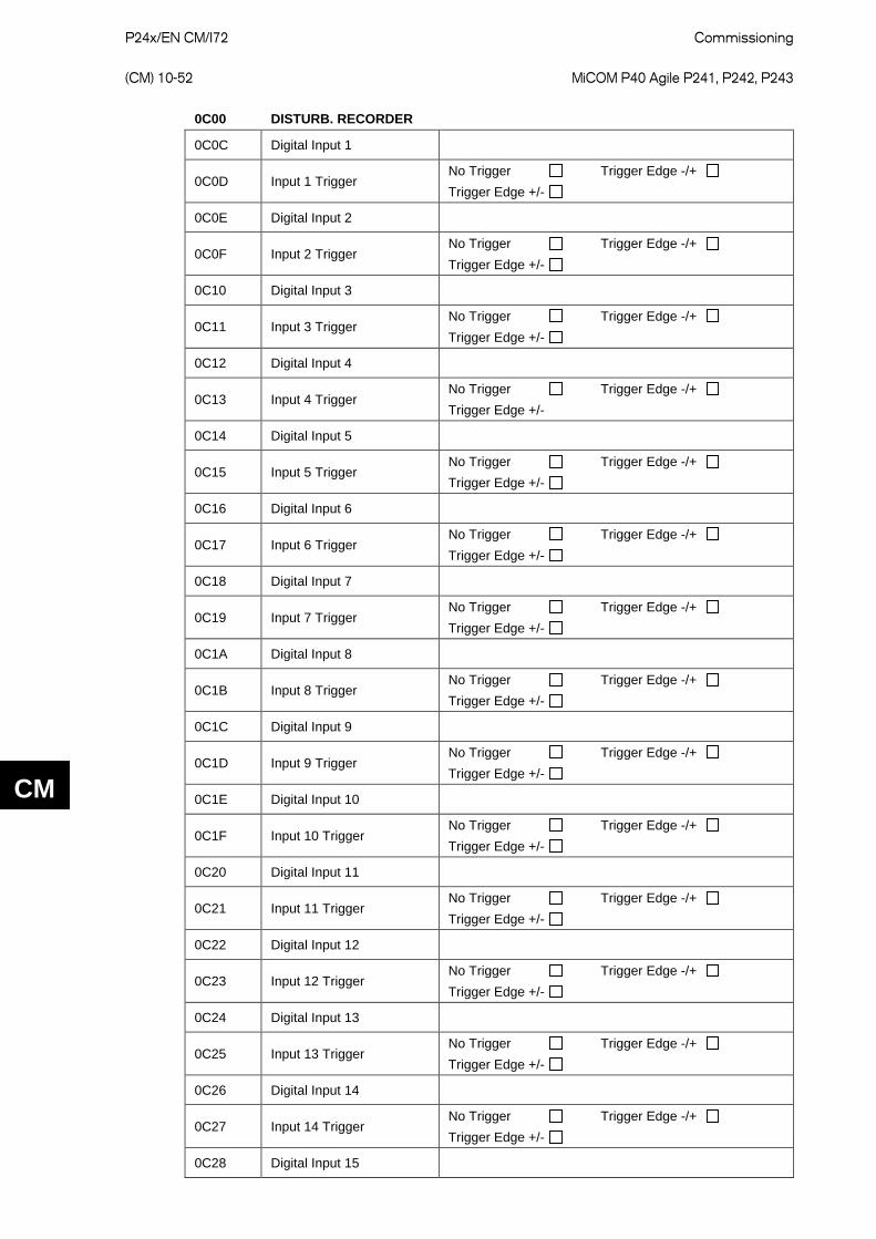
P24x/EN CM/I72
Commissioning (CM) 10-52 MiCOM P40 Agile P241, P242, P243
CM
0C00 DISTURB. RECORDER
0C0C Digital Input 1
0C0D Input 1 Trigger No Trigger Trigger Edge -/+ Trigger Edge +/-
0C0E Digital Input 2
0C0F Input 2 Trigger No Trigger Trigger Edge -/+ Trigger Edge +/-
0C10 Digital Input 3
0C11 Input 3 Trigger No Trigger Trigger Edge -/+ Trigger Edge +/-
0C12 Digital Input 4
0C13 Input 4 Trigger No Trigger Trigger Edge -/+ Trigger Edge +/-
0C14 Digital Input 5
0C15 Input 5 Trigger No Trigger Trigger Edge -/+ Trigger Edge +/-
0C16 Digital Input 6
0C17 Input 6 Trigger No Trigger Trigger Edge -/+ Trigger Edge +/-
0C18 Digital Input 7
0C19 Input 7 Trigger No Trigger Trigger Edge -/+ Trigger Edge +/-
0C1A Digital Input 8
0C1B Input 8 Trigger No Trigger Trigger Edge -/+ Trigger Edge +/-
0C1C Digital Input 9
0C1D Input 9 Trigger No Trigger Trigger Edge -/+ Trigger Edge +/-
0C1E Digital Input 10
0C1F Input 10 Trigger No Trigger Trigger Edge -/+ Trigger Edge +/-
0C20 Digital Input 11
0C21 Input 11 Trigger No Trigger Trigger Edge -/+ Trigger Edge +/-
0C22 Digital Input 12
0C23 Input 12 Trigger No Trigger Trigger Edge -/+ Trigger Edge +/-
0C24 Digital Input 13
0C25 Input 13 Trigger No Trigger Trigger Edge -/+ Trigger Edge +/-
0C26 Digital Input 14
0C27 Input 14 Trigger No Trigger Trigger Edge -/+ Trigger Edge +/-
0C28 Digital Input 15
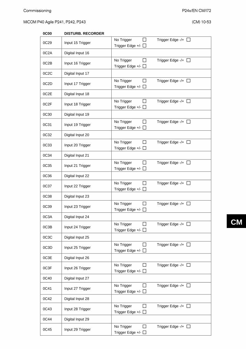
Commissioning
P24x/EN CM/I72 MiCOM P40 Agile P241, P242, P243 (CM) 10-53
CM
0C00 DISTURB. RECORDER
0C29 Input 15 Trigger No Trigger Trigger Edge -/+ Trigger Edge +/-
0C2A Digital Input 16
0C2B Input 16 Trigger No Trigger Trigger Edge -/+ Trigger Edge +/-
0C2C Digital Input 17
0C2D Input 17 Trigger No Trigger Trigger Edge -/+ Trigger Edge +/-
0C2E Digital Input 18
0C2F Input 18 Trigger No Trigger Trigger Edge -/+ Trigger Edge +/-
0C30 Digital Input 19
0C31 Input 19 Trigger No Trigger Trigger Edge -/+ Trigger Edge +/-
0C32 Digital Input 20
0C33 Input 20 Trigger No Trigger Trigger Edge -/+ Trigger Edge +/-
0C34 Digital Input 21
0C35 Input 21 Trigger No Trigger Trigger Edge -/+ Trigger Edge +/-
0C36 Digital Input 22
0C37 Input 22 Trigger No Trigger Trigger Edge -/+ Trigger Edge +/-
0C38 Digital Input 23
0C39 Input 23 Trigger No Trigger Trigger Edge -/+ Trigger Edge +/-
0C3A Digital Input 24
0C3B Input 24 Trigger No Trigger Trigger Edge -/+ Trigger Edge +/-
0C3C Digital Input 25
0C3D Input 25 Trigger No Trigger Trigger Edge -/+ Trigger Edge +/-
0C3E Digital Input 26
0C3F Input 26 Trigger No Trigger Trigger Edge -/+ Trigger Edge +/-
0C40 Digital Input 27
0C41 Input 27 Trigger No Trigger Trigger Edge -/+ Trigger Edge +/-
0C42 Digital Input 28
0C43 Input 28 Trigger No Trigger Trigger Edge -/+ Trigger Edge +/-
0C44 Digital Input 29
0C45 Input 29 Trigger No Trigger Trigger Edge -/+ Trigger Edge +/-
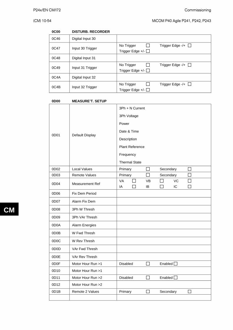
P24x/EN CM/I72
Commissioning (CM) 10-54 MiCOM P40 Agile P241, P242, P243
CM
0C00 DISTURB. RECORDER
0C46 Digital Input 30
0C47 Input 30 Trigger No Trigger Trigger Edge -/+ Trigger Edge +/-
0C48 Digital Input 31
0C49 Input 31 Trigger No Trigger Trigger Edge -/+ Trigger Edge +/-
0C4A Digital Input 32
0C4B Input 32 Trigger No Trigger Trigger Edge -/+ Trigger Edge +/-
0D00 MEASURE’T. SETUP
0D01 Default Display
3Ph + N Current
3Ph Voltage
Power
Date & Time
Description
Plant Reference
Frequency
Thermal State
0D02 Local Values Primary Secondary
0D03 Remote Values Primary Secondary
0D04 Measurement Ref VA VB VC IA IB IC
0D06 Fix Dem Period
0D07 Alarm Fix Dem
0D08 3Ph W Thresh
0D09 3Ph VAr Thresh
0D0A Alarm Energies
0D0B W Fwd Thresh
0D0C W Rev Thresh
0D0D VAr Fwd Thresh
0D0E VAr Rev Thresh
0D0F Motor Hour Run >1 Disabled Enabled
0D10 Motor Hour Run >1
0D11 Motor Hour Run >2 Disabled Enabled
0D12 Motor Hour Run >2
0D1B Remote 2 Values Primary Secondary
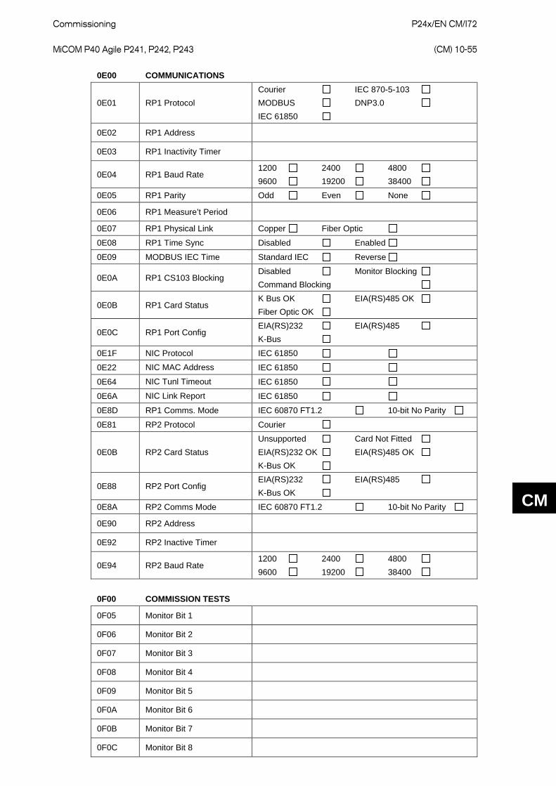
Commissioning
P24x/EN CM/I72 MiCOM P40 Agile P241, P242, P243 (CM) 10-55
CM
0E00 COMMUNICATIONS
0E01 RP1 Protocol Courier IEC 870-5-103 MODBUS DNP3.0 IEC 61850
0E02 RP1 Address
0E03 RP1 Inactivity Timer
0E04 RP1 Baud Rate 1200 2400 4800 9600 19200 38400
0E05 RP1 Parity Odd Even None
0E06 RP1 Measure’t Period
0E07 RP1 Physical Link Copper Fiber Optic
0E08 RP1 Time Sync Disabled Enabled
0E09 MODBUS IEC Time Standard IEC Reverse
0E0A RP1 CS103 Blocking Disabled Monitor Blocking Command Blocking
0E0B RP1 Card Status K Bus OK EIA(RS)485 OK Fiber Optic OK
0E0C RP1 Port Config EIA(RS)232 EIA(RS)485 K-Bus
0E1F NIC Protocol IEC 61850
0E22 NIC MAC Address IEC 61850
0E64 NIC Tunl Timeout IEC 61850
0E6A NIC Link Report IEC 61850
0E8D RP1 Comms. Mode IEC 60870 FT1.2 10-bit No Parity
0E81 RP2 Protocol Courier
0E0B RP2 Card Status Unsupported Card Not Fitted EIA(RS)232 OK EIA(RS)485 OK K-Bus OK
0E88 RP2 Port Config EIA(RS)232 EIA(RS)485 K-Bus OK
0E8A RP2 Comms Mode IEC 60870 FT1.2 10-bit No Parity
0E90 RP2 Address
0E92 RP2 Inactive Timer
0E94 RP2 Baud Rate 1200 2400 4800 9600 19200 38400
0F00 COMMISSION TESTS
0F05 Monitor Bit 1
0F06 Monitor Bit 2
0F07 Monitor Bit 3
0F08 Monitor Bit 4
0F09 Monitor Bit 5
0F0A Monitor Bit 6
0F0B Monitor Bit 7
0F0C Monitor Bit 8

P24x/EN CM/I72
Commissioning (CM) 10-56 MiCOM P40 Agile P241, P242, P243
CM
0F0D Test Mode Test Mode Contacts Blocked
0F0E Test Pattern
1000 CB MONITOR SETUP
1001 Broken Ι^
1002 Ι^ Maintenance Alarm Disabled Alarm Enabled
1003 Ι^ Maintenance
1006 Nb CB Ops Maint Alarm Disabled Alarm Enabled
1007 Nb CB Ops Maint
100A CB Time Maint Alarm Disabled Alarm Enabled
100B CB Time Maint
1100 OPTO CONFIG
1101 Global Nominal V
24 - 27 V 30 - 34 V 48 - 54 V 110 - 125 V 220 - 250 V
Custom
1102 Opto Input 1 24 - 27 V 30 - 34 V 48 - 54 V 110 - 125 V 220 - 250 V
1103 Opto Input 2 24 - 27 V 30 - 34 V 48 - 54 V 110 - 125 V 220 - 250 V
1104 Opto Input 3 24 - 27 V 30 - 34 V 48 - 54 V 110 - 125 V 220 - 250 V
1105 Opto Input 4 24 - 27 V 30 - 34 V 48 - 54 V 110 - 125 V 220 - 250 V
1106 Opto Input 5 24 - 27 V 30 - 34 V 48 - 54 V 110 - 125 V 220 - 250 V
1107 Opto Input 6 24 - 27V 30 - 34 V 48 - 54 V 110 - 125 V 220 - 250 V
1108 Opto Input 7 24 - 27 V 30 - 34 V 48 - 54 V 110 - 125 V 220 - 250 V
1109 Opto Input 8 24 - 27 V 30 - 34 V 48 - 54 V 110 - 125 V 220 - 250 V
110A Opto Input 9 24 - 27 V 30 - 34 V 48 - 54 V 110 - 125 V 220 - 250 V
110B Opto Input 10 24 - 27 V 30 - 34 V 48 - 54 V 110 - 125 V 220 - 250 V
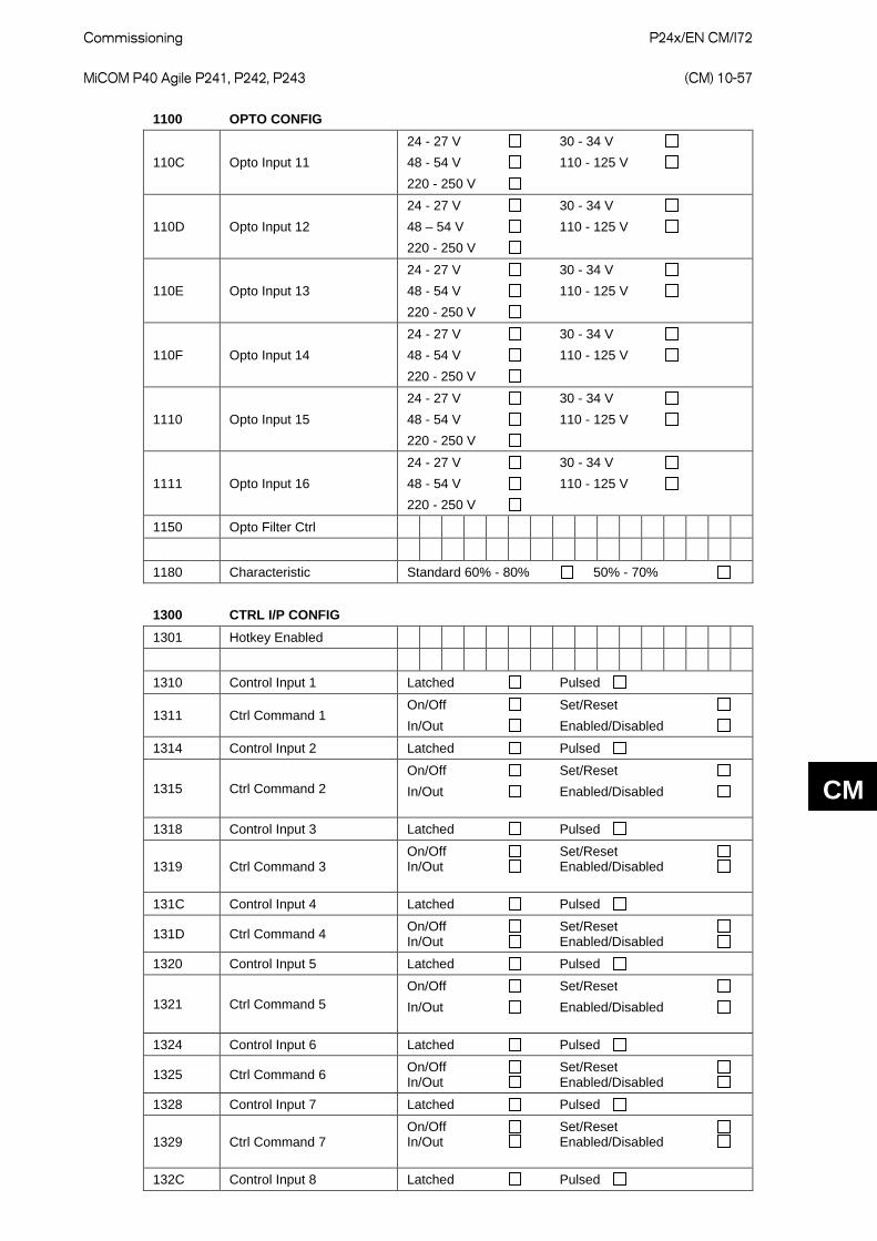
Commissioning
P24x/EN CM/I72 MiCOM P40 Agile P241, P242, P243 (CM) 10-57
CM
1100 OPTO CONFIG
110C Opto Input 11 24 - 27 V 30 - 34 V 48 - 54 V 110 - 125 V 220 - 250 V
110D Opto Input 12 24 - 27 V 30 - 34 V 48 – 54 V 110 - 125 V 220 - 250 V
110E Opto Input 13 24 - 27 V 30 - 34 V 48 - 54 V 110 - 125 V 220 - 250 V
110F Opto Input 14 24 - 27 V 30 - 34 V 48 - 54 V 110 - 125 V 220 - 250 V
1110 Opto Input 15 24 - 27 V 30 - 34 V 48 - 54 V 110 - 125 V 220 - 250 V
1111 Opto Input 16 24 - 27 V 30 - 34 V 48 - 54 V 110 - 125 V 220 - 250 V
1150 Opto Filter Ctrl
1180 Characteristic Standard 60% - 80% 50% - 70%
1300 CTRL I/P CONFIG 1301 Hotkey Enabled
1310 Control Input 1 Latched Pulsed
1311 Ctrl Command 1 On/Off Set/Reset In/Out Enabled/Disabled
1314 Control Input 2 Latched Pulsed
1315 Ctrl Command 2 On/Off Set/Reset In/Out Enabled/Disabled
1318 Control Input 3 Latched Pulsed
1319 Ctrl Command 3 On/Off Set/Reset In/Out Enabled/Disabled
131C Control Input 4 Latched Pulsed
131D Ctrl Command 4 On/Off Set/Reset In/Out Enabled/Disabled
1320 Control Input 5 Latched Pulsed
1321 Ctrl Command 5 On/Off Set/Reset In/Out Enabled/Disabled
1324 Control Input 6 Latched Pulsed
1325 Ctrl Command 6 On/Off Set/Reset In/Out Enabled/Disabled
1328 Control Input 7 Latched Pulsed
1329 Ctrl Command 7 On/Off Set/Reset In/Out Enabled/Disabled
132C Control Input 8 Latched Pulsed
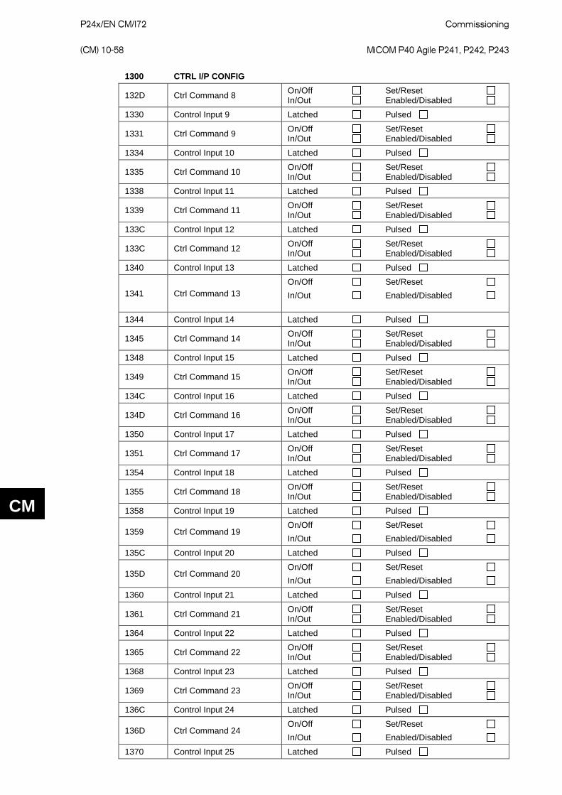
P24x/EN CM/I72
Commissioning (CM) 10-58 MiCOM P40 Agile P241, P242, P243
CM
1300 CTRL I/P CONFIG
132D Ctrl Command 8 On/Off Set/Reset In/Out Enabled/Disabled
1330 Control Input 9 Latched Pulsed
1331 Ctrl Command 9 On/Off Set/Reset In/Out Enabled/Disabled
1334 Control Input 10 Latched Pulsed
1335 Ctrl Command 10 On/Off Set/Reset In/Out Enabled/Disabled
1338 Control Input 11 Latched Pulsed
1339 Ctrl Command 11 On/Off Set/Reset In/Out Enabled/Disabled
133C Control Input 12 Latched Pulsed
133C Ctrl Command 12 On/Off Set/Reset In/Out Enabled/Disabled
1340 Control Input 13 Latched Pulsed
1341 Ctrl Command 13 On/Off Set/Reset In/Out Enabled/Disabled
1344 Control Input 14 Latched Pulsed
1345 Ctrl Command 14 On/Off Set/Reset In/Out Enabled/Disabled
1348 Control Input 15 Latched Pulsed
1349 Ctrl Command 15 On/Off Set/Reset In/Out Enabled/Disabled
134C Control Input 16 Latched Pulsed
134D Ctrl Command 16 On/Off Set/Reset In/Out Enabled/Disabled
1350 Control Input 17 Latched Pulsed
1351 Ctrl Command 17 On/Off Set/Reset In/Out Enabled/Disabled
1354 Control Input 18 Latched Pulsed
1355 Ctrl Command 18 On/Off Set/Reset In/Out Enabled/Disabled
1358 Control Input 19 Latched Pulsed
1359 Ctrl Command 19 On/Off Set/Reset In/Out Enabled/Disabled
135C Control Input 20 Latched Pulsed
135D Ctrl Command 20 On/Off Set/Reset In/Out Enabled/Disabled
1360 Control Input 21 Latched Pulsed
1361 Ctrl Command 21 On/Off Set/Reset In/Out Enabled/Disabled
1364 Control Input 22 Latched Pulsed
1365 Ctrl Command 22 On/Off Set/Reset In/Out Enabled/Disabled
1368 Control Input 23 Latched Pulsed
1369 Ctrl Command 23 On/Off Set/Reset In/Out Enabled/Disabled
136C Control Input 24 Latched Pulsed
136D Ctrl Command 24 On/Off Set/Reset In/Out Enabled/Disabled
1370 Control Input 25 Latched Pulsed
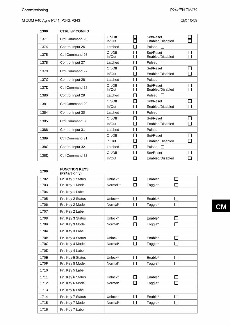
Commissioning
P24x/EN CM/I72 MiCOM P40 Agile P241, P242, P243 (CM) 10-59
CM
1300 CTRL I/P CONFIG
1371 Ctrl Command 25 On/Off Set/Reset In/Out Enabled/Disabled
1374 Control Input 26 Latched Pulsed
1375 Ctrl Command 26 On/Off Set/Reset In/Out Enabled/Disabled
1378 Control Input 27 Latched Pulsed
1379 Ctrl Command 27 On/Off Set/Reset In/Out Enabled/Disabled
137C Control Input 28 Latched Pulsed
137D Ctrl Command 28 On/Off Set/Reset In/Out Enabled/Disabled
1380 Control Input 29 Latched Pulsed
1381 Ctrl Command 29 On/Off Set/Reset In/Out Enabled/Disabled
1384 Control Input 30 Latched Pulsed
1385 Ctrl Command 30 On/Off Set/Reset In/Out Enabled/Disabled
1388 Control Input 31 Latched Pulsed
1389 Ctrl Command 31 On/Off Set/Reset
In/Out Enabled/Disabled
138C Control Input 32 Latched Pulsed
138D Ctrl Command 32 On/Off Set/Reset In/Out Enabled/Disabled
1700 FUNCTION KEYS (P242/3 only)
1702 Fn. Key 1 Status Unlock* Enable*
1703 Fn. Key 1 Mode Normal * Toggle*
1704 Fn. Key 1 Label
1705 Fn. Key 2 Status Unlock* Enable*
1706 Fn. Key 2 Mode Normal* Toggle*
1707 Fn. Key 2 Label
1708 Fn. Key 3 Status Unlock* Enable*
1709 Fn. Key 3 Mode Normal* Toggle*
170A Fn. Key 3 Label
170B Fn. Key 4 Status Unlock* Enable*
170C Fn. Key 4 Mode Normal* Toggle*
170D Fn. Key 4 Label
170E Fn. Key 5 Status Unlock* Enable*
170F Fn. Key 5 Mode Normal* Toggle*
1710 Fn. Key 5 Label
1711 Fn. Key 6 Status Unlock* Enable*
1712 Fn. Key 6 Mode Normal* Toggle*
1713 Fn. Key 6 Label
1714 Fn. Key 7 Status Unlock* Enable*
1715 Fn. Key 7 Mode Normal* Toggle*
1716 Fn. Key 7 Label
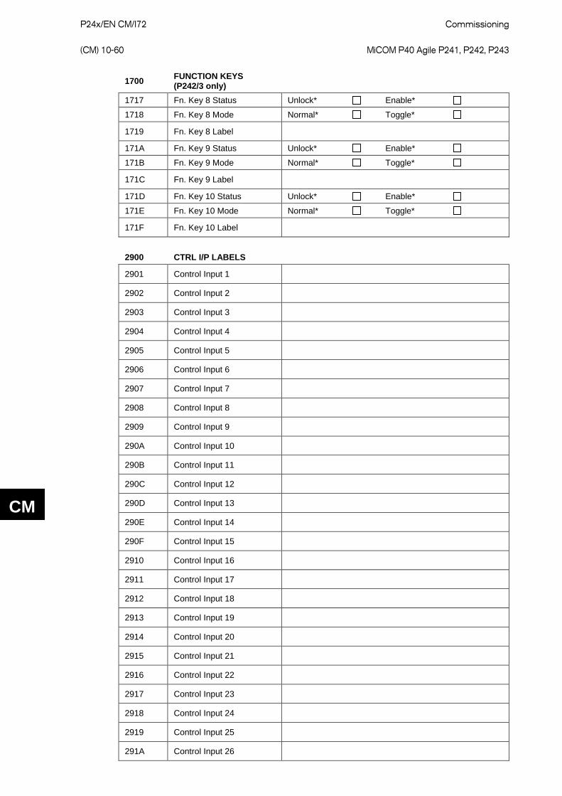
P24x/EN CM/I72
Commissioning (CM) 10-60 MiCOM P40 Agile P241, P242, P243
CM
1700 FUNCTION KEYS (P242/3 only)
1717 Fn. Key 8 Status Unlock* Enable*
1718 Fn. Key 8 Mode Normal* Toggle*
1719 Fn. Key 8 Label
171A Fn. Key 9 Status Unlock* Enable*
171B Fn. Key 9 Mode Normal* Toggle*
171C Fn. Key 9 Label
171D Fn. Key 10 Status Unlock* Enable*
171E Fn. Key 10 Mode Normal* Toggle*
171F Fn. Key 10 Label
2900 CTRL I/P LABELS
2901 Control Input 1
2902 Control Input 2
2903 Control Input 3
2904 Control Input 4
2905 Control Input 5
2906 Control Input 6
2907 Control Input 7
2908 Control Input 8
2909 Control Input 9
290A Control Input 10
290B Control Input 11
290C Control Input 12
290D Control Input 13
290E Control Input 14
290F Control Input 15
2910 Control Input 16
2911 Control Input 17
2912 Control Input 18
2913 Control Input 19
2914 Control Input 20
2915 Control Input 21
2916 Control Input 22
2917 Control Input 23
2918 Control Input 24
2919 Control Input 25
291A Control Input 26
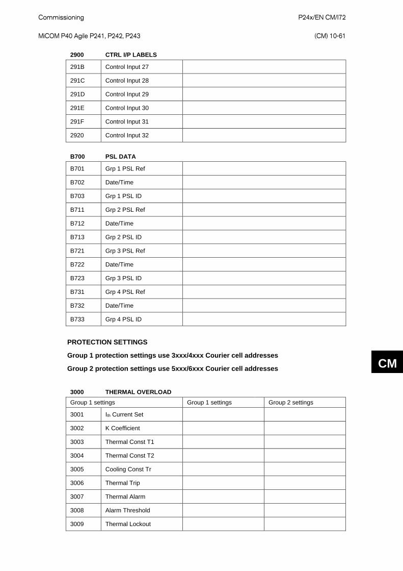
Commissioning
P24x/EN CM/I72 MiCOM P40 Agile P241, P242, P243 (CM) 10-61
CM
2900 CTRL I/P LABELS
291B Control Input 27
291C Control Input 28
291D Control Input 29
291E Control Input 30
291F Control Input 31
2920 Control Input 32
B700 PSL DATA
B701 Grp 1 PSL Ref
B702 Date/Time
B703 Grp 1 PSL ID
B711 Grp 2 PSL Ref
B712 Date/Time
B713 Grp 2 PSL ID
B721 Grp 3 PSL Ref
B722 Date/Time
B723 Grp 3 PSL ID
B731 Grp 4 PSL Ref
B732 Date/Time
B733 Grp 4 PSL ID
PROTECTION SETTINGS
Group 1 protection settings use 3xxx/4xxx Courier cell addresses
Group 2 protection settings use 5xxx/6xxx Courier cell addresses
3000 THERMAL OVERLOAD Group 1 settings Group 1 settings Group 2 settings
3001 Ith Current Set
3002 K Coefficient
3003 Thermal Const T1
3004 Thermal Const T2
3005 Cooling Const Tr
3006 Thermal Trip
3007 Thermal Alarm
3008 Alarm Threshold
3009 Thermal Lockout
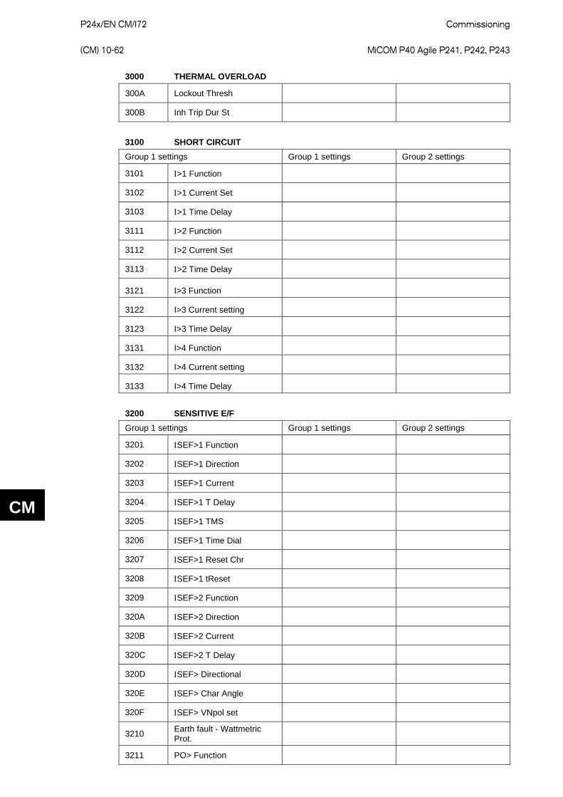
P24x/EN CM/I72
Commissioning (CM) 10-62 MiCOM P40 Agile P241, P242, P243
CM
3000 THERMAL OVERLOAD
300A Lockout Thresh
300B Inh Trip Dur St
3100 SHORT CIRCUIT Group 1 settings Group 1 settings Group 2 settings
3101 Ι>1 Function
3102 Ι>1 Current Set
3103 Ι>1 Time Delay
3111 Ι>2 Function
3112 Ι>2 Current Set
3113 Ι>2 Time Delay
3121 I>3 Function
3122 I>3 Current setting
3123 I>3 Time Delay
3131 I>4 Function
3132 I>4 Current setting
3133 I>4 Time Delay
3200 SENSITIVE E/F Group 1 settings Group 1 settings Group 2 settings
3201 ΙSEF>1 Function
3202 ΙSEF>1 Direction
3203 ΙSEF>1 Current
3204 ΙSEF>1 T Delay
3205 ΙSEF>1 TMS
3206 ΙSEF>1 Time Dial
3207 ΙSEF>1 Reset Chr
3208 ΙSEF>1 tReset
3209 ΙSEF>2 Function
320A ΙSEF>2 Direction
320B ΙSEF>2 Current
320C ΙSEF>2 T Delay
320D ΙSEF> Directional
320E ΙSEF> Char Angle
320F ΙSEF> VNpol set
3210 Earth fault - Wattmetric Prot.
3211 PO> Function
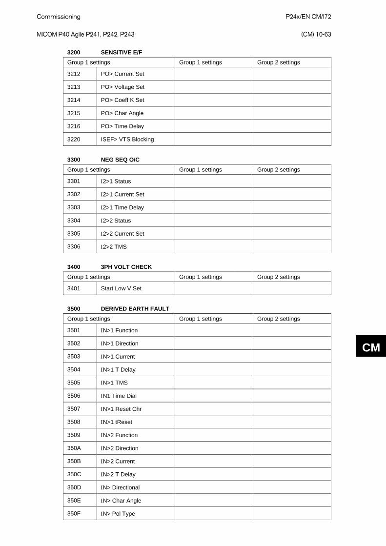
Commissioning
P24x/EN CM/I72 MiCOM P40 Agile P241, P242, P243 (CM) 10-63
CM
3200 SENSITIVE E/F Group 1 settings Group 1 settings Group 2 settings
3212 PO> Current Set
3213 PO> Voltage Set
3214 PO> Coeff K Set
3215 PO> Char Angle
3216 PO> Time Delay
3220 ISEF> VTS Blocking
3300 NEG SEQ O/C Group 1 settings Group 1 settings Group 2 settings
3301 Ι2>1 Status
3302 Ι2>1 Current Set
3303 Ι2>1 Time Delay
3304 Ι2>2 Status
3305 Ι2>2 Current Set
3306 Ι2>2 TMS
3400 3PH VOLT CHECK Group 1 settings Group 1 settings Group 2 settings
3401 Start Low V Set
3500 DERIVED EARTH FAULT Group 1 settings Group 1 settings Group 2 settings
3501 ΙN>1 Function
3502 ΙN>1 Direction
3503 ΙN>1 Current
3504 ΙN>1 T Delay
3505 ΙN>1 TMS
3506 ΙN1 Time Dial
3507 ΙN>1 Reset Chr
3508 ΙN>1 tReset
3509 ΙN>2 Function
350A ΙN>2 Direction
350B ΙN>2 Current
350C ΙN>2 T Delay
350D ΙN> Directional
350E ΙN> Char Angle
350F ΙN> Pol Type

P24x/EN CM/I72
Commissioning (CM) 10-64 MiCOM P40 Agile P241, P242, P243
CM
3500 DERIVED EARTH FAULT Group 1 settings Group 1 settings Group 2 settings
3510 ΙN> VN pol set
3511 ΙN2> V2pol set
3512 ΙN2> I2pol set
3520 ΙN> VTS Blocking
3600 NEG SEQ O/V Group 1 settings Group 1 settings Group 2 settings
3601 V2>1 Status
3602 V2>1 Voltage Set
3603 V2>1 Time Delay
3611 V2>2 Status
3612 V2>2 Voltage Set
3613 V2>2 Time Delay
3900 STALL PROTECTION Group 1 settings Group 1 settings Group 2 settings
3901 Prolonged Start
3902 Start Criteria
3903 Starting Current
3904 Prol Start Time
3905 Stall Rotor-strt
3906 Stall Detection
3907 Stall Setting
3908 Stall Time
3909 Reacceleration
390A Reacc Low V Set
390B LV Ride Thru
390C Reac. High V Set
390D Reac. Time
390E Auto Re-start
390F Reac. Long Time
3910 Reac. Shed Time
3A00 DIFFERENTIAL Group 1 settings Group 1 settings Group 2 settings
3A01 Diff Function
3A02 Diff Ιs1
3A03 Diff k1
3A04 Diff Ιs2
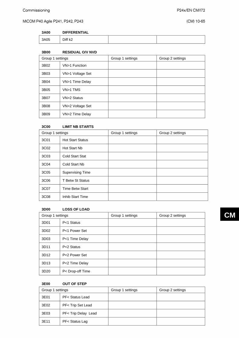
Commissioning
P24x/EN CM/I72 MiCOM P40 Agile P241, P242, P243 (CM) 10-65
CM
3A00 DIFFERENTIAL
3A05 Diff k2
3B00 RESIDUAL O/V NVD Group 1 settings Group 1 settings Group 2 settings
3B02 VN>1 Function
3B03 VN>1 Voltage Set
3B04 VN>1 Time Delay
3B05 VN>1 TMS
3B07 VN>2 Status
3B08 VN>2 Voltage Set
3B09 VN>2 Time Delay
3C00 LIMIT NB STARTS Group 1 settings Group 1 settings Group 2 settings
3C01 Hot Start Status
3C02 Hot Start Nb
3C03 Cold Start Stat
3C04 Cold Start Nb
3C05 Supervising Time
3C06 T Betw St Status
3C07 Time Betw Start
3C08 Inhib Start Time
3D00 LOSS OF LOAD Group 1 settings Group 1 settings Group 2 settings
3D01 P<1 Status
3D02 P<1 Power Set
3D03 P<1 Time Delay
3D11 P<2 Status
3D12 P<2 Power Set
3D13 P<2 Time Delay
3D20 P< Drop-off Time
3E00 OUT OF STEP Group 1 settings Group 1 settings Group 2 settings
3E01 PF< Status Lead
3E02 PF< Trip Set Lead
3E03 PF< Trip Delay Lead
3E11 PF< Status Lag
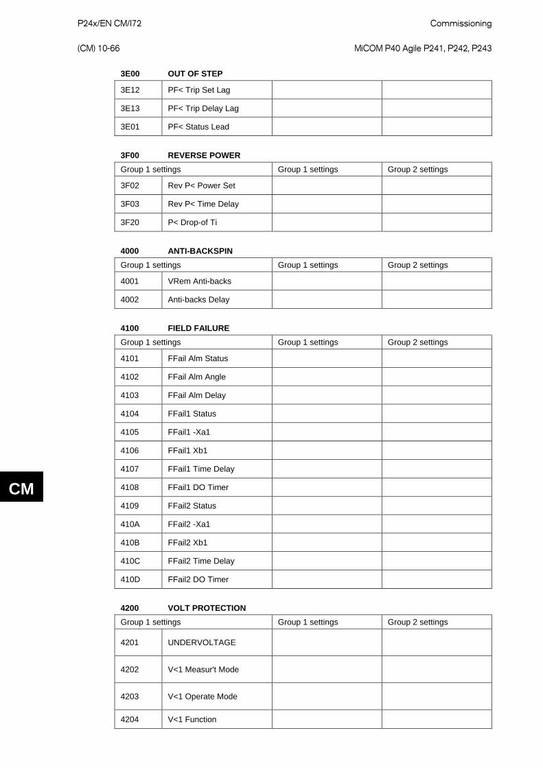
P24x/EN CM/I72
Commissioning (CM) 10-66 MiCOM P40 Agile P241, P242, P243
CM
3E00 OUT OF STEP
3E12 PF< Trip Set Lag
3E13 PF< Trip Delay Lag
3E01 PF< Status Lead
3F00 REVERSE POWER Group 1 settings Group 1 settings Group 2 settings
3F02 Rev P< Power Set
3F03 Rev P< Time Delay
3F20 P< Drop-of Ti
4000 ANTI-BACKSPIN Group 1 settings Group 1 settings Group 2 settings
4001 VRem Anti-backs
4002 Anti-backs Delay
4100 FIELD FAILURE Group 1 settings Group 1 settings Group 2 settings
4101 FFail Alm Status
4102 FFail Alm Angle
4103 FFail Alm Delay
4104 FFail1 Status
4105 FFail1 -Xa1
4106 FFail1 Xb1
4107 FFail1 Time Delay
4108 FFail1 DO Timer
4109 FFail2 Status
410A FFail2 -Xa1
410B FFail2 Xb1
410C FFail2 Time Delay
410D FFail2 DO Timer
4200 VOLT PROTECTION Group 1 settings Group 1 settings Group 2 settings
4201 UNDERVOLTAGE
4202 V<1 Measur't Mode
4203 V<1 Operate Mode
4204 V<1 Function
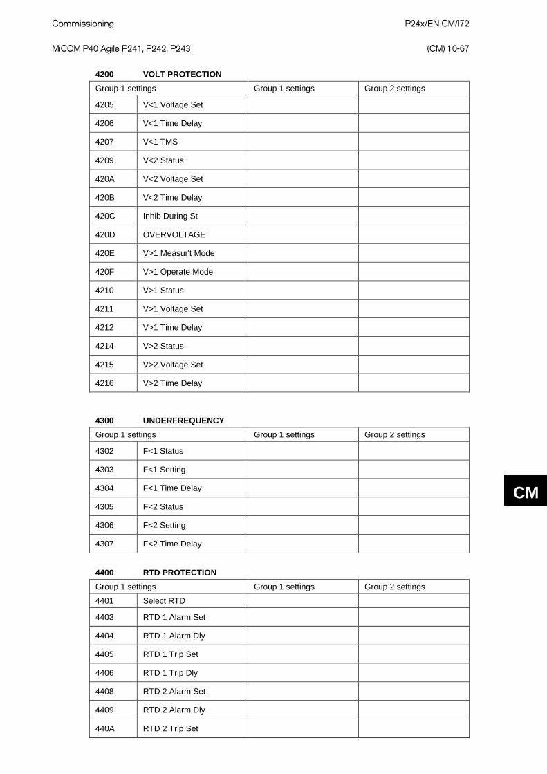
Commissioning
P24x/EN CM/I72 MiCOM P40 Agile P241, P242, P243 (CM) 10-67
CM
4200 VOLT PROTECTION Group 1 settings Group 1 settings Group 2 settings
4205 V<1 Voltage Set
4206 V<1 Time Delay
4207 V<1 TMS
4209 V<2 Status
420A V<2 Voltage Set
420B V<2 Time Delay
420C Inhib During St
420D OVERVOLTAGE
420E V>1 Measur't Mode
420F V>1 Operate Mode
4210 V>1 Status
4211 V>1 Voltage Set
4212 V>1 Time Delay
4214 V>2 Status
4215 V>2 Voltage Set
4216 V>2 Time Delay
4300 UNDERFREQUENCY Group 1 settings Group 1 settings Group 2 settings
4302 F<1 Status
4303 F<1 Setting
4304 F<1 Time Delay
4305 F<2 Status
4306 F<2 Setting
4307 F<2 Time Delay
4400 RTD PROTECTION Group 1 settings Group 1 settings Group 2 settings
4401 Select RTD
4403 RTD 1 Alarm Set
4404 RTD 1 Alarm Dly
4405 RTD 1 Trip Set
4406 RTD 1 Trip Dly
4408 RTD 2 Alarm Set
4409 RTD 2 Alarm Dly
440A RTD 2 Trip Set
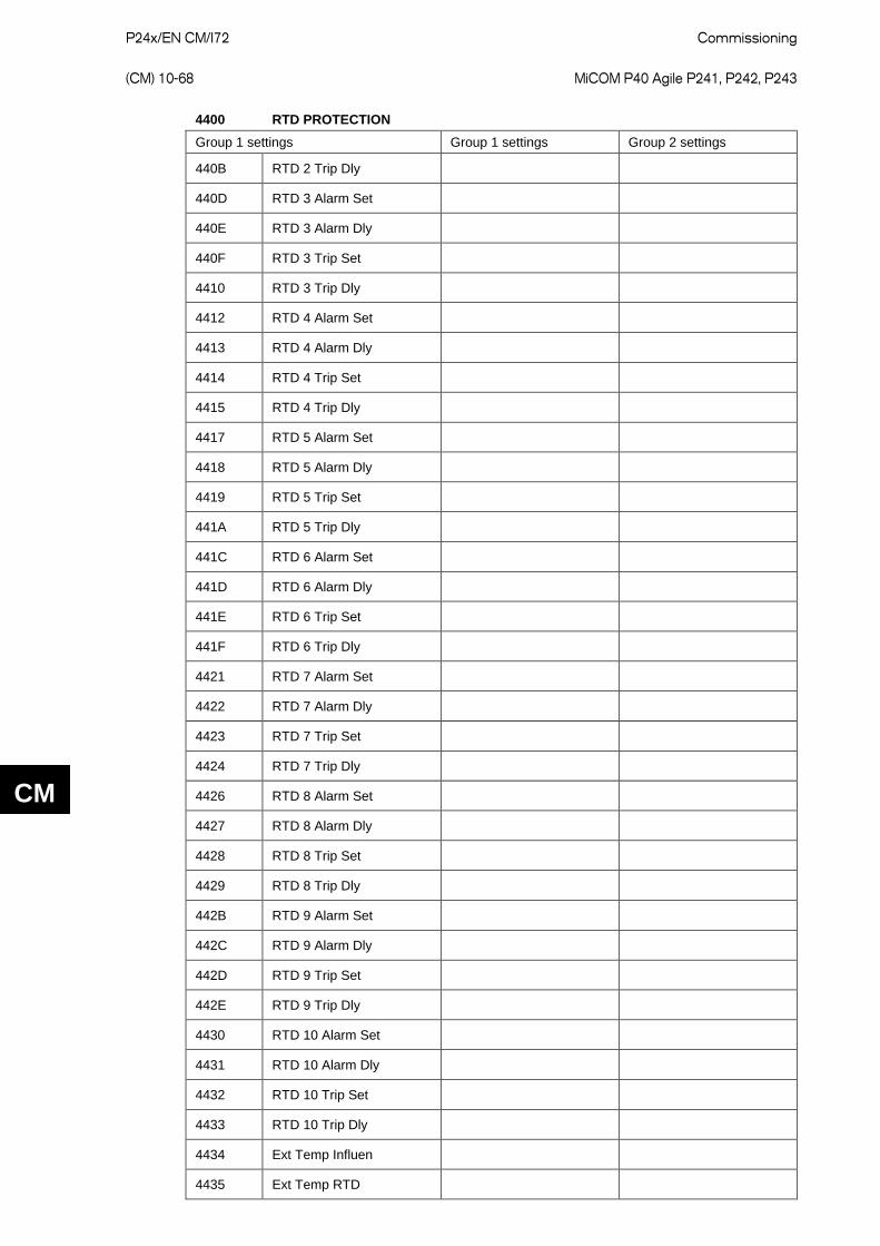
P24x/EN CM/I72
Commissioning (CM) 10-68 MiCOM P40 Agile P241, P242, P243
CM
4400 RTD PROTECTION Group 1 settings Group 1 settings Group 2 settings
440B RTD 2 Trip Dly
440D RTD 3 Alarm Set
440E RTD 3 Alarm Dly
440F RTD 3 Trip Set
4410 RTD 3 Trip Dly
4412 RTD 4 Alarm Set
4413 RTD 4 Alarm Dly
4414 RTD 4 Trip Set
4415 RTD 4 Trip Dly
4417 RTD 5 Alarm Set
4418 RTD 5 Alarm Dly
4419 RTD 5 Trip Set
441A RTD 5 Trip Dly
441C RTD 6 Alarm Set
441D RTD 6 Alarm Dly
441E RTD 6 Trip Set
441F RTD 6 Trip Dly
4421 RTD 7 Alarm Set
4422 RTD 7 Alarm Dly
4423 RTD 7 Trip Set
4424 RTD 7 Trip Dly
4426 RTD 8 Alarm Set
4427 RTD 8 Alarm Dly
4428 RTD 8 Trip Set
4429 RTD 8 Trip Dly
442B RTD 9 Alarm Set
442C RTD 9 Alarm Dly
442D RTD 9 Trip Set
442E RTD 9 Trip Dly
4430 RTD 10 Alarm Set
4431 RTD 10 Alarm Dly
4432 RTD 10 Trip Set
4433 RTD 10 Trip Dly
4434 Ext Temp Influen
4435 Ext Temp RTD
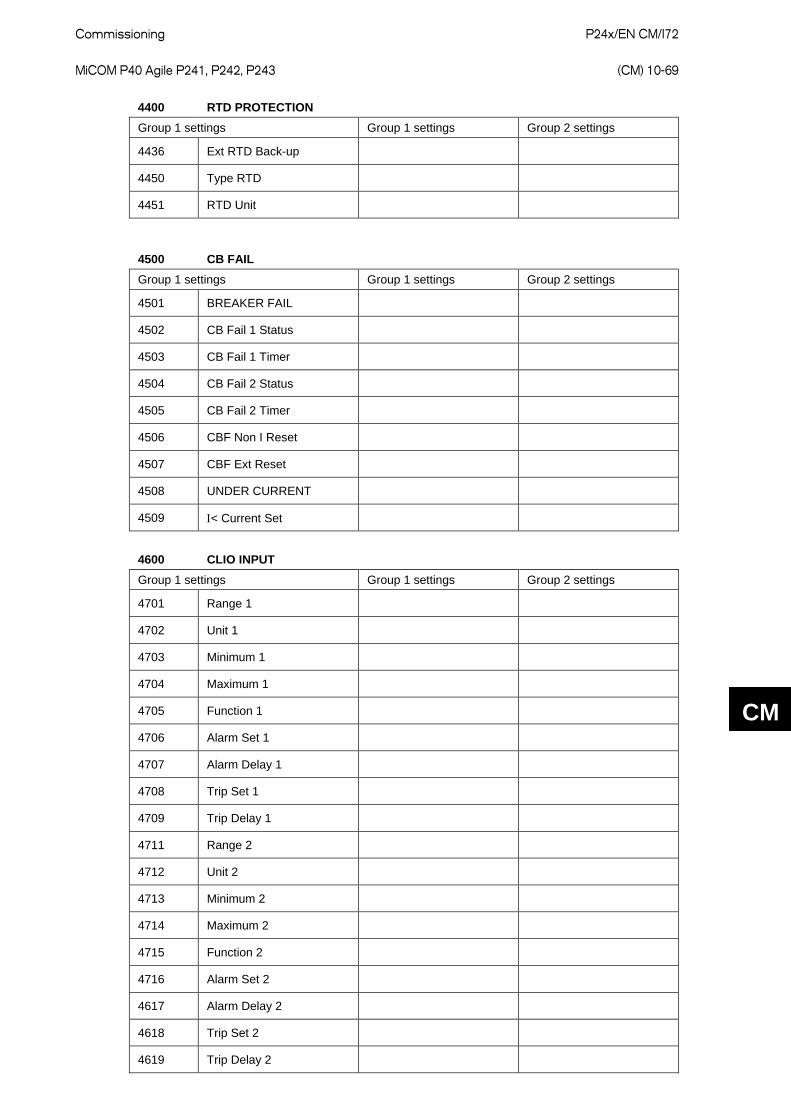
Commissioning
P24x/EN CM/I72 MiCOM P40 Agile P241, P242, P243 (CM) 10-69
CM
4400 RTD PROTECTION Group 1 settings Group 1 settings Group 2 settings
4436 Ext RTD Back-up
4450 Type RTD
4451 RTD Unit
4500 CB FAIL Group 1 settings Group 1 settings Group 2 settings
4501 BREAKER FAIL
4502 CB Fail 1 Status
4503 CB Fail 1 Timer
4504 CB Fail 2 Status
4505 CB Fail 2 Timer
4506 CBF Non I Reset
4507 CBF Ext Reset
4508 UNDER CURRENT
4509 Ι< Current Set
4600 CLIO INPUT Group 1 settings Group 1 settings Group 2 settings
4701 Range 1
4702 Unit 1
4703 Minimum 1
4704 Maximum 1
4705 Function 1
4706 Alarm Set 1
4707 Alarm Delay 1
4708 Trip Set 1
4709 Trip Delay 1
4711 Range 2
4712 Unit 2
4713 Minimum 2
4714 Maximum 2
4715 Function 2
4716 Alarm Set 2
4617 Alarm Delay 2
4618 Trip Set 2
4619 Trip Delay 2
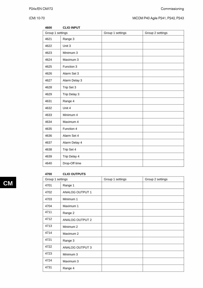
P24x/EN CM/I72
Commissioning (CM) 10-70 MiCOM P40 Agile P241, P242, P243
CM
4600 CLIO INPUT Group 1 settings Group 1 settings Group 2 settings
4621 Range 3
4622 Unit 3
4623 Minimum 3
4624 Maximum 3
4625 Function 3
4626 Alarm Set 3
4627 Alarm Delay 3
4628 Trip Set 3
4629 Trip Delay 3
4631 Range 4
4632 Unit 4
4633 Minimum 4
4634 Maximum 4
4635 Function 4
4636 Alarm Set 4
4637 Alarm Delay 4
4638 Trip Set 4
4639 Trip Delay 4
4640 Drop-Off time
4700 CLIO OUTPUTS Group 1 settings Group 1 settings Group 2 settings
4701 Range 1
4702 ANALOG OUTPUT 1
4703 Minimum 1
4704 Maximum 1
4711 Range 2
4712 ANALOG OUTPUT 2
4713 Minimum 2
4714 Maximum 2
4721 Range 3
4722 ANALOG OUTPUT 3
4723 Minimum 3
4724 Maximum 3
4731 Range 4
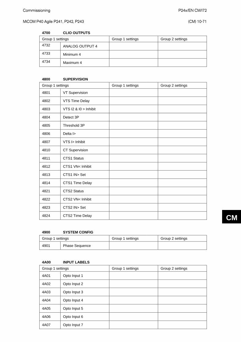
Commissioning
P24x/EN CM/I72 MiCOM P40 Agile P241, P242, P243 (CM) 10-71
CM
4700 CLIO OUTPUTS Group 1 settings Group 1 settings Group 2 settings
4732 ANALOG OUTPUT 4
4733 Minimum 4
4734 Maximum 4
4800 SUPERVISION Group 1 settings Group 1 settings Group 2 settings
4801 VT Supervision
4802 VTS Time Delay
4803 VTS I2 & I0 > Inhibit
4804 Detect 3P
4805 Threshold 3P
4806 Delta I>
4807 VTS I> Inhibit
4810 CT Supervision
4811 CTS1 Status
4812 CTS1 VN< Inhibit
4813 CTS1 IN> Set
4814 CTS1 Time Delay
4821 CTS2 Status
4822 CTS2 VN< Inhibit
4823 CTS2 IN> Set
4824 CTS2 Time Delay
4900 SYSTEM CONFIG Group 1 settings Group 1 settings Group 2 settings
4901 Phase Sequence
4A00 INPUT LABELS Group 1 settings Group 1 settings Group 2 settings
4A01 Opto Input 1
4A02 Opto Input 2
4A03 Opto Input 3
4A04 Opto Input 4
4A05 Opto Input 5
4A06 Opto Input 6
4A07 Opto Input 7
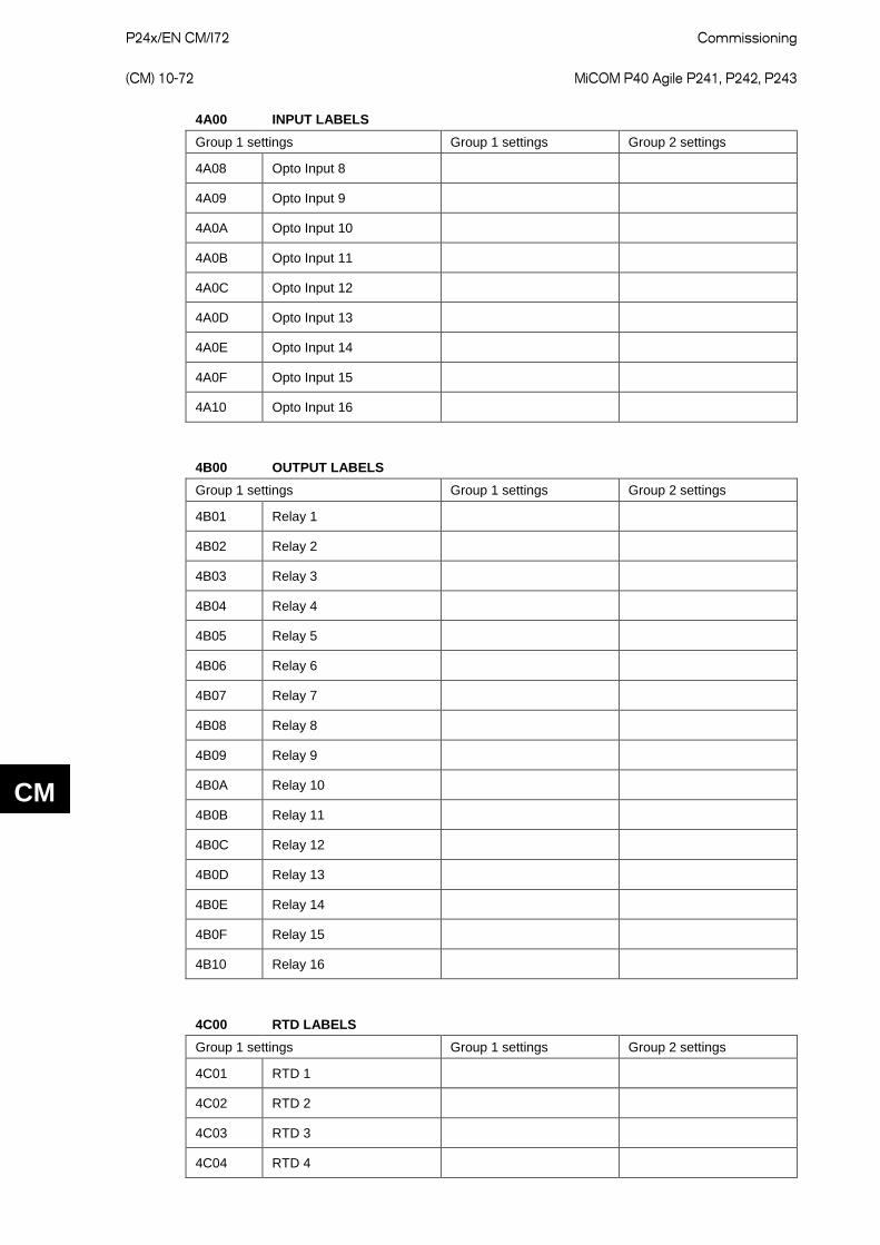
P24x/EN CM/I72
Commissioning (CM) 10-72 MiCOM P40 Agile P241, P242, P243
CM
4A00 INPUT LABELS Group 1 settings Group 1 settings Group 2 settings
4A08 Opto Input 8
4A09 Opto Input 9
4A0A Opto Input 10
4A0B Opto Input 11
4A0C Opto Input 12
4A0D Opto Input 13
4A0E Opto Input 14
4A0F Opto Input 15
4A10 Opto Input 16
4B00 OUTPUT LABELS Group 1 settings Group 1 settings Group 2 settings
4B01 Relay 1
4B02 Relay 2
4B03 Relay 3
4B04 Relay 4
4B05 Relay 5
4B06 Relay 6
4B07 Relay 7
4B08 Relay 8
4B09 Relay 9
4B0A Relay 10
4B0B Relay 11
4B0C Relay 12
4B0D Relay 13
4B0E Relay 14
4B0F Relay 15
4B10 Relay 16
4C00 RTD LABELS Group 1 settings Group 1 settings Group 2 settings
4C01 RTD 1
4C02 RTD 2
4C03 RTD 3
4C04 RTD 4
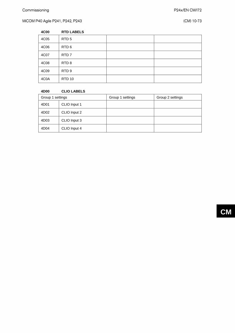
Commissioning
P24x/EN CM/I72 MiCOM P40 Agile P241, P242, P243 (CM) 10-73
CM
4C00 RTD LABELS
4C05 RTD 5
4C06 RTD 6
4C07 RTD 7
4C08 RTD 8
4C09 RTD 9
4C0A RTD 10
4D00 CLIO LABELS Group 1 settings Group 1 settings Group 2 settings
4D01 CLIO Input 1
4D02 CLIO Input 2
4D03 CLIO Input 3
4D04 CLIO Input 4

P24x/EN CM/I72
Commissioning (CM) 10-74 MiCOM P40 Agile P241, P242, P243
CM
Maintenance
P24x/EN MT/I72 MiCOM P40 Agile P241, P242, P243 (MT) 11-1
MT
MAINTENANCE

P24x/EN MT/I72
Maintenance (MT) 11-2 MiCOM P40 Agile P241, P242, P243
MT

Maintenance
P24x/EN MT/I72 MiCOM P40 Agile P241, P242, P243 (MT) 11-3
MT
CONTENTS
1 MAINTENANCE 5
1.1 Maintenance period 5
1.2 Maintenance checks 5
1.2.1 Alarms 5
1.2.2 Opto-isolators 5
1.2.3 Output relays 5
1.2.4 Measurement accuracy 5
1.3 Method of repair 6
1.3.1 Replacing the complete relay 6
1.3.2 Replacing a PCB 7
1.3.2.1 Replacement of the main processor board 10
1.3.2.2 Replacement of the IRIG-B/2nd rear communications, Ethernet board 11
1.3.2.3 Replacement of the input module 14
1.3.2.4 Replacement of the power supply board 15
1.3.2.5 Replacement of the relay board in the power supply module 16
1.3.2.6 Replacement of the opto and separate relay boards (P241/2/3) 16
1.3.2.7 Replacement of the RTD input board 17
1.3.2.8 Replacement of the CLIO input board 19
1.4 Re-calibration 19
1.5 Changing the battery 19
1.5.1 Instructions for replacing the battery 20
1.5.2 Post modification tests 20
1.5.3 Battery disposal 20
1.6 Cleaning 20
FIGURES Figure 1: Location of securing screws for terminal blocks 7
Figure 2: Front panel assembly 11
Figure 3: Location of securing screws for IRIG-B board 12
Figure 4: Typical IRIG-B board 13
Figure 5: Second rear communications board with IRIG-B 13
Figure 6: Location of securing screws for input module 14
Figure 7: Typical power supply board 15
Figure 8: Typical relay board 16
Figure 9: Typical opto board 17
Figure 10: Location of securing screws for RTD/CLIO input board 18
Figure 11: Typical RTD input board 18

P24x/EN MT/I72
Maintenance (MT) 11-4 MiCOM P40 Agile P241, P242, P243
MT
TABLES Table 1: PCB part numbers 10
Maintenance
P24x/EN MT/I72 MiCOM P40 Agile P241, P242, P243 (MT) 11-5
MT
1 MAINTENANCE
1.1 Maintenance period It is recommended that products supplied by General Electric receive periodic monitoring after installation. As with all products some deterioration with time is inevitable. Due to the critical nature of protective relays and their infrequent operation, it is necessary to confirm regularly that they are operating correctly.
General Electric protective relays are designed for life in excess of 20 years.
MiCOM P24x motor relays are self-supervising and so require less maintenance than earlier designs of relay. Most problems result in an alarm so that remedial action can be taken. However, some periodic tests should be done to ensure the relay is functioning correctly and the external wiring is intact.
If the customer’s organization has a Preventative Maintenance Policy, the recommended product checks should be included in the regular program. Maintenance periods will depend on many factors, such as:
• The operating environment • The accessibility of the site • The amount of available manpower • The importance of the installation in the power system • The consequences of failure
1.2 Maintenance checks Although some functionality checks can be performed from a remote location by using the communications ability of the relays, these are mainly restricted to checking the relay is measuring the applied currents and voltages accurately, and checking the circuit breaker maintenance counters. Therefore it is recommended that maintenance checks are performed locally (i.e. at the substation itself).
Before carrying out any work on the equipment, the user should be familiar with the contents of the Safety and Technical Data chapters and the ratings on the equipment’s rating label.
Before carrying out any work on the equipment the user should be familiar with the contents of the Safety Section/Safety Guide Pxxx-SG-4LM-2 or later issue and the ratings on the equipment’s rating label.
1.2.1 Alarms Check the alarm status LED to identify if any alarm conditions exist. If the LED is ON, press the read key [] repeatedly to step through the alarms. Clear the alarms to switch the LED OFF.
1.2.2 Opto-isolators Check the relay responds when the opto-isolated inputs are energized. See section 5.2.6 of P24x/EN CM.
1.2.3 Output relays Check the output relays operate. See section 5.2.7 of P24x/EN CM.
1.2.4 Measurement accuracy If the power system is energized, compare the values measured by the relay with known system values to check that they are in the approximate range. If they are, the relay is performing the analog-to-digital conversion and calculations correctly. See sections 7.1 and 7.2 of P24x/EN CM.
Alternatively, check the values measured by the relay against known values injected into the relay using the test block, if fitted, or injected directly into the relay terminals. See sections
P24x/EN MT/I72
Maintenance (MT) 11-6 MiCOM P40 Agile P241, P242, P243
MT
5.2.13 and 5.2.14 of P24x/EN CM. These tests prove the calibration accuracy is being maintained.
1.3 Method of repair If the relay develops a fault while in service, depending on the type of fault, the watchdog contacts change state and an alarm condition is flagged. Due to the extensive use of surface-mount components faulty PCBs cannot be repaired and should be replaced. Therefore replace the complete relay or just the faulty PCB identified by the in-built diagnostic software. Advice about identifying the faulty PCB can be found in ‘Problem Analysis’.
The preferred method is to replace the complete relay. This ensures the internal circuitry is protected against electrostatic discharge and physical damage at all times and avoids incompatibility between replacement PCBs. However, it may be difficult to remove an installed relay due to limited access in the back of the cubicle and rigidity of the scheme wiring.
Replacing PCBs can reduce transport costs but requires clean, dry conditions on site and higher skills from the person performing the repair. However, if the repair is not performed by an approved service center, the warranty will be invalidated.
Before carrying out any work on the equipment the user should be familiar with the contents of the Safety Section/Safety Guide Pxxx-SG-4LM-2 or later issue and the ratings on the equipment’s rating label. This should ensure that no damage is caused by incorrect handling of the electronic components.
1.3.1 Replacing the complete relay The case and rear terminal blocks are designed to ease removal of the complete relay, without having to disconnect the scheme wiring.
Before working at the rear of the relay, isolate all voltage and current supplies to the relay.
Note: The MiCOM range of relays have integral current transformer shorting switches which will close when the heavy duty terminal block is removed.
Disconnect the relay earth connection from the rear of the relay.
Maintenance
P24x/EN MT/I72 MiCOM P40 Agile P241, P242, P243 (MT) 11-7
MT
Figure 1: Location of securing screws for terminal blocks
There are three types of terminal block used on the relay, RTD/CLIO input, heavy duty and medium duty. The terminal blocks are fastened to the rear panel using slotted screws on RTD/CLIO input blocks and crosshead on the heavy and medium duty blocks. See Figure 1.
Note: The use of a magnetic bladed screwdriver is recommended to minimize the risk of the screws being left in the terminal block or lost.
Without exerting excessive force or damaging the scheme wiring, pull the terminal blocks away from their internal connectors.
Remove the screws used to fasten the relay to the panel and rack. These are the screws with the larger diameter heads that are accessible with the access covers are fitted and open.
If the top and bottom access covers have been removed, do not remove the screws with the smaller diameter heads which are accessible. These screws hold the front panel on the relay.
Withdraw the relay from the pane and rack. Be careful because the relay is heavy due to the internal transformers, particularly the P243.
To reinstall the repaired or replacement relay follow the above instructions in reverse, ensuring that each terminal block is relocated in the correct position and the case earth, IRIG-B and fiber optic connections are replaced. To help identify each terminal block, they are labeled alphabetically with ‘A’ on the left hand side when viewed from the rear.
Once reinstallation is complete, recommission the relay. See sections 1 to 7 in chapter P24x/EN CM.
1.3.2 Replacing a PCB Replacing printed circuit boards and other internal components of protective relays must be undertaken only by Service Centers approved by General Electric. Failure to obtain the authorization of General Electric After Sales Engineers prior to commencing work may invalidate the product warranty.
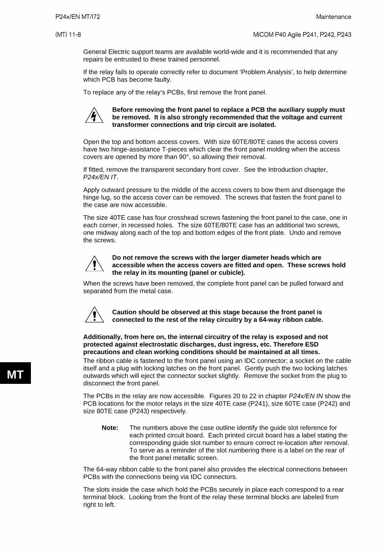
P24x/EN MT/I72
Maintenance (MT) 11-8 MiCOM P40 Agile P241, P242, P243
MT
General Electric support teams are available world-wide and it is recommended that any repairs be entrusted to these trained personnel.
If the relay fails to operate correctly refer to document ‘Problem Analysis’, to help determine which PCB has become faulty.
To replace any of the relay’s PCBs, first remove the front panel.
Before removing the front panel to replace a PCB the auxiliary supply must be removed. It is also strongly recommended that the voltage and current transformer connections and trip circuit are isolated.
Open the top and bottom access covers. With size 60TE/80TE cases the access covers have two hinge-assistance T-pieces which clear the front panel molding when the access covers are opened by more than 90°, so allowing their removal.
If fitted, remove the transparent secondary front cover. See the Introduction chapter, P24x/EN IT.
Apply outward pressure to the middle of the access covers to bow them and disengage the hinge lug, so the access cover can be removed. The screws that fasten the front panel to the case are now accessible.
The size 40TE case has four crosshead screws fastening the front panel to the case, one in each corner, in recessed holes. The size 60TE/80TE case has an additional two screws, one midway along each of the top and bottom edges of the front plate. Undo and remove the screws.
Do not remove the screws with the larger diameter heads which are accessible when the access covers are fitted and open. These screws hold the relay in its mounting (panel or cubicle).
When the screws have been removed, the complete front panel can be pulled forward and separated from the metal case.
Caution should be observed at this stage because the front panel is connected to the rest of the relay circuitry by a 64-way ribbon cable.
Additionally, from here on, the internal circuitry of the relay is exposed and not protected against electrostatic discharges, dust ingress, etc. Therefore ESD precautions and clean working conditions should be maintained at all times. The ribbon cable is fastened to the front panel using an IDC connector; a socket on the cable itself and a plug with locking latches on the front panel. Gently push the two locking latches outwards which will eject the connector socket slightly. Remove the socket from the plug to disconnect the front panel.
The PCBs in the relay are now accessible. Figures 20 to 22 in chapter P24x/EN IN show the PCB locations for the motor relays in the size 40TE case (P241), size 60TE case (P242) and size 80TE case (P243) respectively.
Note: The numbers above the case outline identify the guide slot reference for each printed circuit board. Each printed circuit board has a label stating the corresponding guide slot number to ensure correct re-location after removal. To serve as a reminder of the slot numbering there is a label on the rear of the front panel metallic screen.
The 64-way ribbon cable to the front panel also provides the electrical connections between PCBs with the connections being via IDC connectors.
The slots inside the case which hold the PCBs securely in place each correspond to a rear terminal block. Looking from the front of the relay these terminal blocks are labeled from right to left.

Maintenance
P24x/EN MT/I72 MiCOM P40 Agile P241, P242, P243 (MT) 11-9
MT
Note: To ensure compatibility, always replace a faulty PCB with one of an identical part number. Table 1 lists the part numbers of each PCB type.
PCB Part number Design suffix Front panel assembly P241 only GN0004 001 A/C
Front panel assembly P242 only GN0006 001 C
Front panel assembly P243 only GN0068 001 C
Front panel assembly P241 only GN0178 001 J
Front panel assembly P242 only GN0277 001 K
Front panel assembly P243 only GN0341 001 K
Power supply board (24/48 V dc) ZN0001 001 A
(48/125 V dc) ZN0001 002 A
(110/250 V dc) ZN0001 003 A
Power supply board (24/48 V dc) ZN0021 001 C/J/K
(48/125 V dc) ZN0021 002 C/J/K
(110/250 V dc) ZN0021 003 C/J/K
Relay board 7 Relay contacts ZN0002 001 A
Relay board 7 Relay contacts ZN0031 001 C/J
Relay board 8 Relay contacts ZN0019 001 C/J/K
Opto board 8 Opto inputs ZN0005 002 A
Opto board 8 Opto inputs ZN0017 002 C
Dual char. opto board 8 Opto inputs ZN0017 012 J/K
Dual char. input/output board 4 Opto inputs + 4 relay contacts ZN0028 011 J
IRIG-B board (comms. assy.) (IRIG-B modulated input only) ZN0007 001 A/C/J/K
(Fiber optic rear comms port only) ZN0007 002 A/C/J/K
(IRIG-B input modulated with fiber optic rear comms port)
ZN0007 003 A/C/J/K
RTD board 10 RTDs ZN0010 002 A
RTD board 10 RTDs ZN0044 002 C/J/K
2nd rear comms. board (2nd rear comms with IRIG-B modulated) ZN0025 001 J/K
2nd rear comms. board (2nd rear comms port only) ZN0025 002 J/K
Ethernet board (Ethernet port only) ZN0049 001 J/K
(Ethernet with IRIG-B modulated) ZN0049 002 J/K
(Ethernet with IRIG-B unmodulated) ZN0049 003 J/K
(IRIG-B unmodulated input only) ZN0049 004 J/K
Redundant Ethernet Self-Healing Ring, 2 multi-mode fiber ports + Modulated IRIG-B
[ZN0071 Part 001] J/K
Redundant Ethernet Self-Healing Ring, 2 multi-mode fiber ports + Un-modulated IRIG-B
[ZN0071 Part 002] J/K
Redundant Ethernet RSTP, 2 multi-mode fiber ports + Modulated
IRIG-B [ZN0071 Part 005] J/K
P24x/EN MT/I72
Maintenance (MT) 11-10 MiCOM P40 Agile P241, P242, P243
MT
PCB Part number Design suffix
Redundant Ethernet RSTP, 2 multi-mode fiber ports + Un-modulated IRIG-B
[ZN0071 Part 006] J/K
Redundant Ethernet Dual-Homing Star, 2 multi-mode fiber ports + Modulated IRIG-B
[ZN0071 Part 007] J/K
Redundant Ethernet Dual-Homing Star, 2 multi-mode fiber ports + Un-modulated IRIG-B
[ZN0071 Part 008] J/K
CLIO board 4 inputs + 4 outputs ZN0018 001 C/J/K
Transformer board ZN0004 001 A/B/C/J/K
Auxiliary transformer board ZN0011 001 A/B/C/J
Input board 8 Opto inputs ZN0005 005 A
Input board 8 Opto inputs ZN0017 003 B/C
Dual char. input board 8 Opto inputs ZN0017 013 J/K
Input module (transformer + auxiliary transformer + input board)
P241 Vn = 100/120 V GN0010 005 GN0010 092
A/C/J
P242 Vn = 100/120 V GN0010 005 GN0010 092
C/K
P243 Vn = 100/120 V GN0012 011 GN0010 029
C/K
Table 1: PCB part numbers
1.3.2.1 Replacement of the main processor board The main processor board is in the front panel. The other PCBs are in the main case of the relay.
Place the front panel with the user interface face-down and remove the six screws from the metallic screen, as shown in Figure 2. Remove the metal plate.
Remove the two screws, either side of the rear of the battery compartment recess, that hold the main processor PCB in position.
The user interface keypad is connected to the main processor board with a flex-strip ribbon cable. Carefully disconnect the ribbon cable at the PCB-mounted connector as it could easily be damaged by excessive twisting.
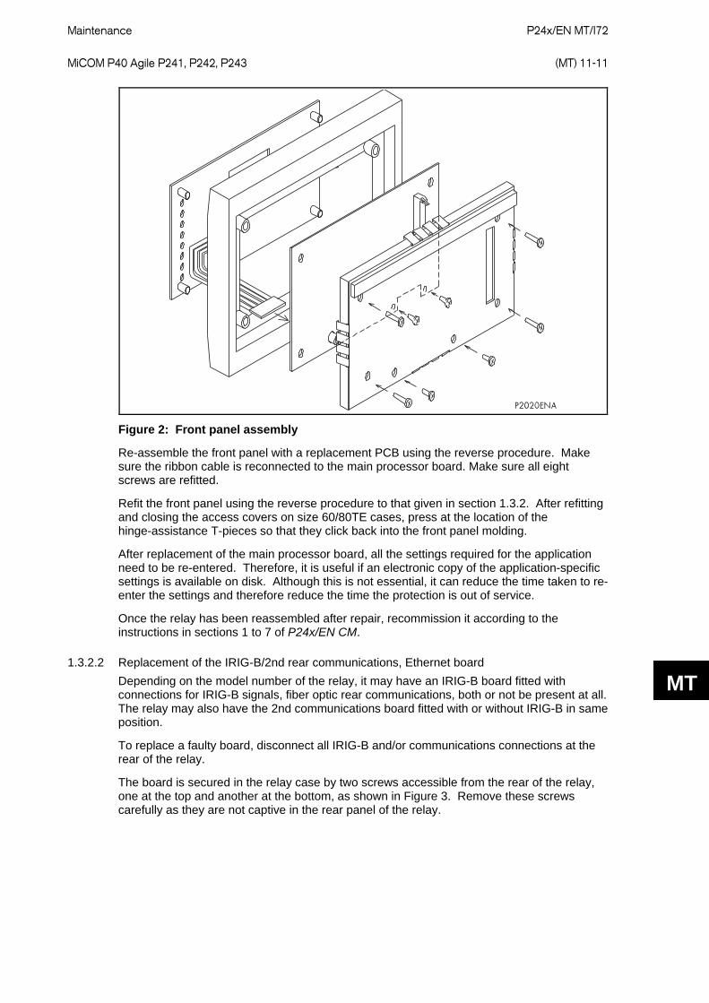
Maintenance
P24x/EN MT/I72 MiCOM P40 Agile P241, P242, P243 (MT) 11-11
MT
Figure 2: Front panel assembly
Re-assemble the front panel with a replacement PCB using the reverse procedure. Make sure the ribbon cable is reconnected to the main processor board. Make sure all eight screws are refitted.
Refit the front panel using the reverse procedure to that given in section 1.3.2. After refitting and closing the access covers on size 60/80TE cases, press at the location of the hinge-assistance T-pieces so that they click back into the front panel molding.
After replacement of the main processor board, all the settings required for the application need to be re-entered. Therefore, it is useful if an electronic copy of the application-specific settings is available on disk. Although this is not essential, it can reduce the time taken to re-enter the settings and therefore reduce the time the protection is out of service.
Once the relay has been reassembled after repair, recommission it according to the instructions in sections 1 to 7 of P24x/EN CM.
1.3.2.2 Replacement of the IRIG-B/2nd rear communications, Ethernet board Depending on the model number of the relay, it may have an IRIG-B board fitted with connections for IRIG-B signals, fiber optic rear communications, both or not be present at all. The relay may also have the 2nd communications board fitted with or without IRIG-B in same position.
To replace a faulty board, disconnect all IRIG-B and/or communications connections at the rear of the relay.
The board is secured in the relay case by two screws accessible from the rear of the relay, one at the top and another at the bottom, as shown in Figure 3. Remove these screws carefully as they are not captive in the rear panel of the relay.
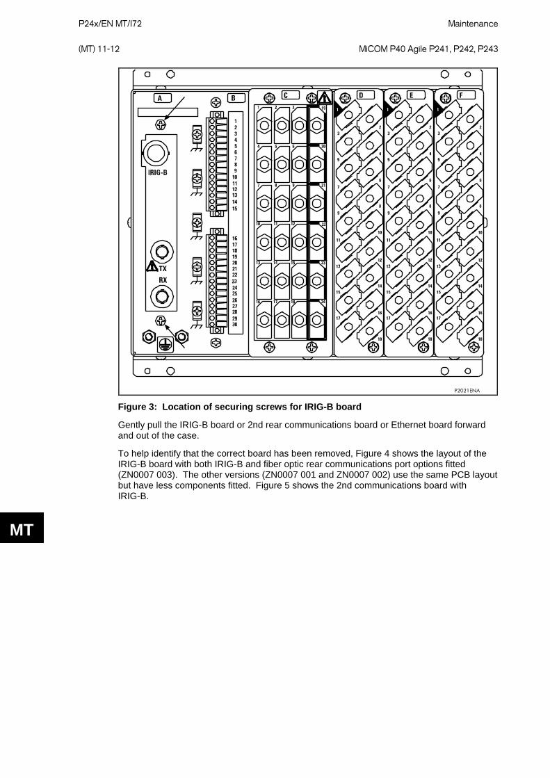
P24x/EN MT/I72
Maintenance (MT) 11-12 MiCOM P40 Agile P241, P242, P243
MT
Figure 3: Location of securing screws for IRIG-B board
Gently pull the IRIG-B board or 2nd rear communications board or Ethernet board forward and out of the case.
To help identify that the correct board has been removed, Figure 4 shows the layout of the IRIG-B board with both IRIG-B and fiber optic rear communications port options fitted (ZN0007 003). The other versions (ZN0007 001 and ZN0007 002) use the same PCB layout but have less components fitted. Figure 5 shows the 2nd communications board with IRIG-B.
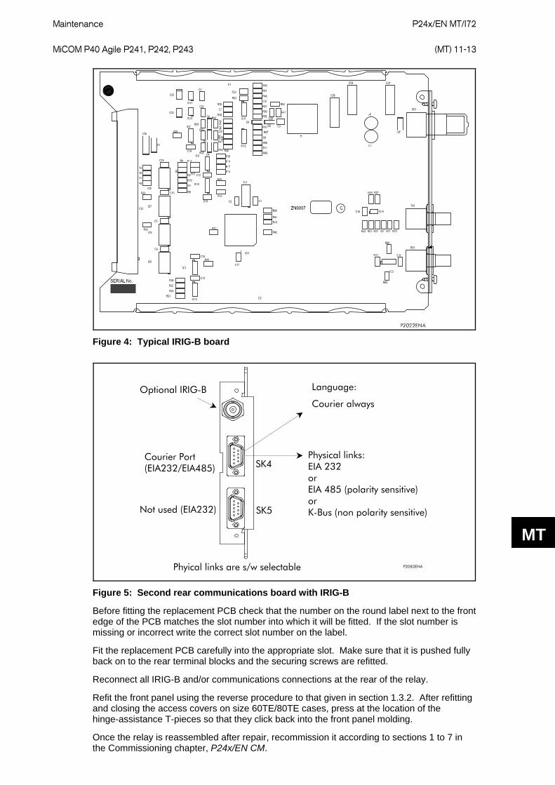
Maintenance
P24x/EN MT/I72 MiCOM P40 Agile P241, P242, P243 (MT) 11-13
MT
Figure 4: Typical IRIG-B board
Language:
Courier always
Physical links:EIA 232 or EIA 485 (polarity sensitive) or K-Bus (non polarity sensitive)SK5
SK4
Phyical links are s/w selectable
Optional IRIG-B
Courier Port (EIA232/EIA485)
Not used (EIA232)
P2083ENA
Figure 5: Second rear communications board with IRIG-B
Before fitting the replacement PCB check that the number on the round label next to the front edge of the PCB matches the slot number into which it will be fitted. If the slot number is missing or incorrect write the correct slot number on the label.
Fit the replacement PCB carefully into the appropriate slot. Make sure that it is pushed fully back on to the rear terminal blocks and the securing screws are refitted.
Reconnect all IRIG-B and/or communications connections at the rear of the relay.
Refit the front panel using the reverse procedure to that given in section 1.3.2. After refitting and closing the access covers on size 60TE/80TE cases, press at the location of the hinge-assistance T-pieces so that they click back into the front panel molding.
Once the relay is reassembled after repair, recommission it according to sections 1 to 7 in the Commissioning chapter, P24x/EN CM.
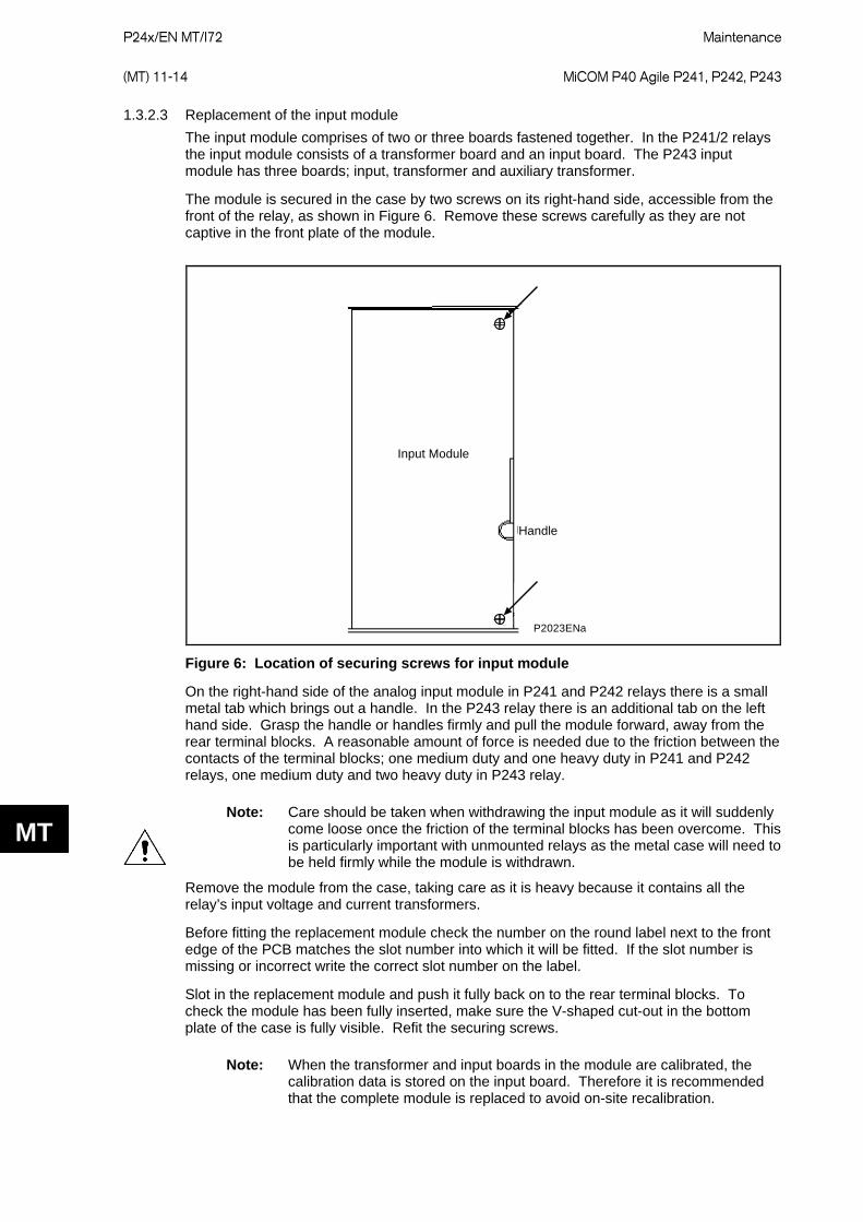
P24x/EN MT/I72
Maintenance (MT) 11-14 MiCOM P40 Agile P241, P242, P243
MT
1.3.2.3 Replacement of the input module The input module comprises of two or three boards fastened together. In the P241/2 relays the input module consists of a transformer board and an input board. The P243 input module has three boards; input, transformer and auxiliary transformer.
The module is secured in the case by two screws on its right-hand side, accessible from the front of the relay, as shown in Figure 6. Remove these screws carefully as they are not captive in the front plate of the module.
Input Module
Handle
P2023ENa
Figure 6: Location of securing screws for input module
On the right-hand side of the analog input module in P241 and P242 relays there is a small metal tab which brings out a handle. In the P243 relay there is an additional tab on the left hand side. Grasp the handle or handles firmly and pull the module forward, away from the rear terminal blocks. A reasonable amount of force is needed due to the friction between the contacts of the terminal blocks; one medium duty and one heavy duty in P241 and P242 relays, one medium duty and two heavy duty in P243 relay.
Note: Care should be taken when withdrawing the input module as it will suddenly come loose once the friction of the terminal blocks has been overcome. This is particularly important with unmounted relays as the metal case will need to be held firmly while the module is withdrawn.
Remove the module from the case, taking care as it is heavy because it contains all the relay’s input voltage and current transformers.
Before fitting the replacement module check the number on the round label next to the front edge of the PCB matches the slot number into which it will be fitted. If the slot number is missing or incorrect write the correct slot number on the label.
Slot in the replacement module and push it fully back on to the rear terminal blocks. To check the module has been fully inserted, make sure the V-shaped cut-out in the bottom plate of the case is fully visible. Refit the securing screws.
Note: When the transformer and input boards in the module are calibrated, the calibration data is stored on the input board. Therefore it is recommended that the complete module is replaced to avoid on-site recalibration.
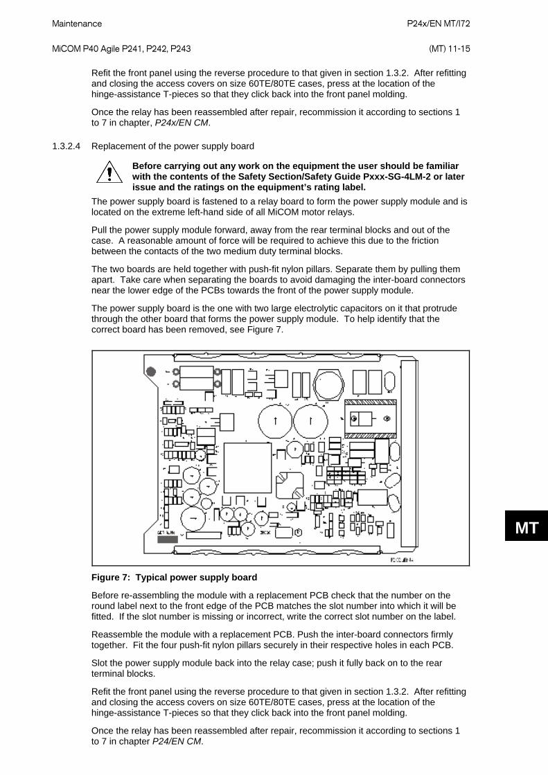
Maintenance
P24x/EN MT/I72 MiCOM P40 Agile P241, P242, P243 (MT) 11-15
MT
Refit the front panel using the reverse procedure to that given in section 1.3.2. After refitting and closing the access covers on size 60TE/80TE cases, press at the location of the hinge-assistance T-pieces so that they click back into the front panel molding.
Once the relay has been reassembled after repair, recommission it according to sections 1 to 7 in chapter, P24x/EN CM.
1.3.2.4 Replacement of the power supply board
Before carrying out any work on the equipment the user should be familiar with the contents of the Safety Section/Safety Guide Pxxx-SG-4LM-2 or later issue and the ratings on the equipment’s rating label.
The power supply board is fastened to a relay board to form the power supply module and is located on the extreme left-hand side of all MiCOM motor relays.
Pull the power supply module forward, away from the rear terminal blocks and out of the case. A reasonable amount of force will be required to achieve this due to the friction between the contacts of the two medium duty terminal blocks.
The two boards are held together with push-fit nylon pillars. Separate them by pulling them apart. Take care when separating the boards to avoid damaging the inter-board connectors near the lower edge of the PCBs towards the front of the power supply module.
The power supply board is the one with two large electrolytic capacitors on it that protrude through the other board that forms the power supply module. To help identify that the correct board has been removed, see Figure 7.
Figure 7: Typical power supply board
Before re-assembling the module with a replacement PCB check that the number on the round label next to the front edge of the PCB matches the slot number into which it will be fitted. If the slot number is missing or incorrect, write the correct slot number on the label.
Reassemble the module with a replacement PCB. Push the inter-board connectors firmly together. Fit the four push-fit nylon pillars securely in their respective holes in each PCB.
Slot the power supply module back into the relay case; push it fully back on to the rear terminal blocks.
Refit the front panel using the reverse procedure to that given in section 1.3.2. After refitting and closing the access covers on size 60TE/80TE cases, press at the location of the hinge-assistance T-pieces so that they click back into the front panel molding.
Once the relay has been reassembled after repair, recommission it according to sections 1 to 7 in chapter P24/EN CM.
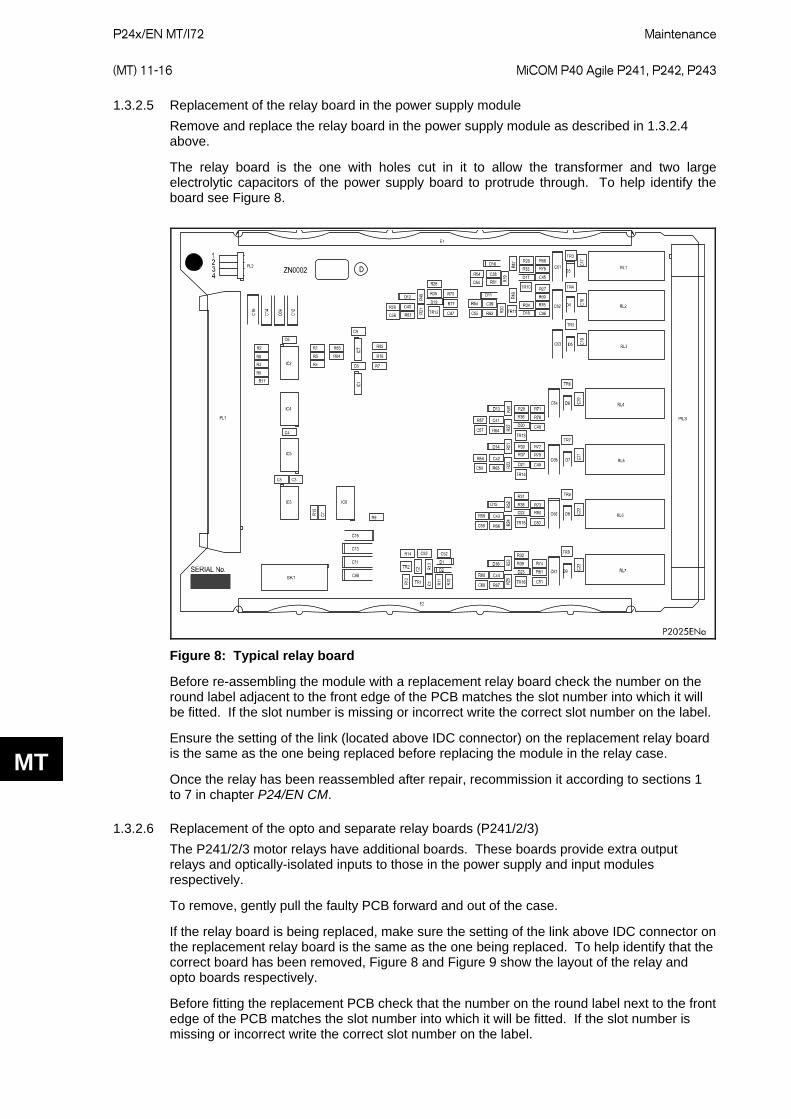
P24x/EN MT/I72
Maintenance (MT) 11-16 MiCOM P40 Agile P241, P242, P243
MT
1.3.2.5 Replacement of the relay board in the power supply module Remove and replace the relay board in the power supply module as described in 1.3.2.4 above.
The relay board is the one with holes cut in it to allow the transformer and two large electrolytic capacitors of the power supply board to protrude through. To help identify the board see Figure 8.
Figure 8: Typical relay board
Before re-assembling the module with a replacement relay board check the number on the round label adjacent to the front edge of the PCB matches the slot number into which it will be fitted. If the slot number is missing or incorrect write the correct slot number on the label.
Ensure the setting of the link (located above IDC connector) on the replacement relay board is the same as the one being replaced before replacing the module in the relay case.
Once the relay has been reassembled after repair, recommission it according to sections 1 to 7 in chapter P24/EN CM.
1.3.2.6 Replacement of the opto and separate relay boards (P241/2/3) The P241/2/3 motor relays have additional boards. These boards provide extra output relays and optically-isolated inputs to those in the power supply and input modules respectively.
To remove, gently pull the faulty PCB forward and out of the case.
If the relay board is being replaced, make sure the setting of the link above IDC connector on the replacement relay board is the same as the one being replaced. To help identify that the correct board has been removed, Figure 8 and Figure 9 show the layout of the relay and opto boards respectively.
Before fitting the replacement PCB check that the number on the round label next to the front edge of the PCB matches the slot number into which it will be fitted. If the slot number is missing or incorrect write the correct slot number on the label.
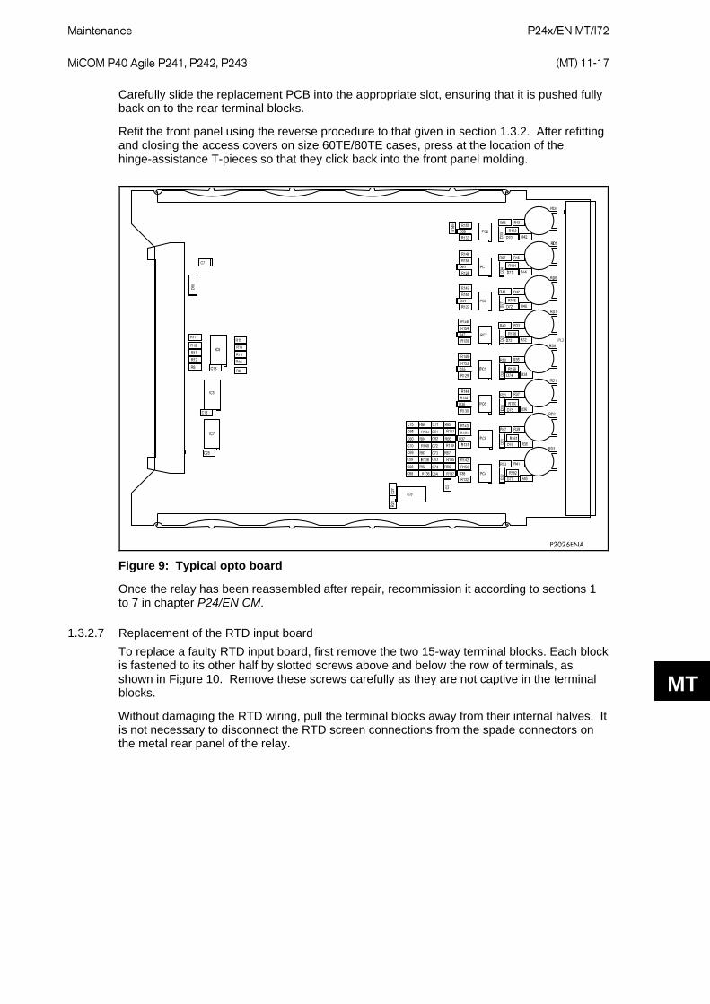
Maintenance
P24x/EN MT/I72 MiCOM P40 Agile P241, P242, P243 (MT) 11-17
MT
Carefully slide the replacement PCB into the appropriate slot, ensuring that it is pushed fully back on to the rear terminal blocks.
Refit the front panel using the reverse procedure to that given in section 1.3.2. After refitting and closing the access covers on size 60TE/80TE cases, press at the location of the hinge-assistance T-pieces so that they click back into the front panel molding.
Figure 9: Typical opto board
Once the relay has been reassembled after repair, recommission it according to sections 1 to 7 in chapter P24/EN CM.
1.3.2.7 Replacement of the RTD input board To replace a faulty RTD input board, first remove the two 15-way terminal blocks. Each block is fastened to its other half by slotted screws above and below the row of terminals, as shown in Figure 10. Remove these screws carefully as they are not captive in the terminal blocks.
Without damaging the RTD wiring, pull the terminal blocks away from their internal halves. It is not necessary to disconnect the RTD screen connections from the spade connectors on the metal rear panel of the relay.
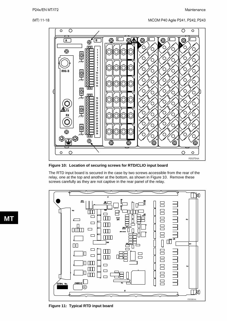
P24x/EN MT/I72
Maintenance (MT) 11-18 MiCOM P40 Agile P241, P242, P243
MT
Figure 10: Location of securing screws for RTD/CLIO input board
The RTD input board is secured in the case by two screws accessible from the rear of the relay, one at the top and another at the bottom, as shown in Figure 10. Remove these screws carefully as they are not captive in the rear panel of the relay.
Figure 11: Typical RTD input board
Maintenance
P24x/EN MT/I72 MiCOM P40 Agile P241, P242, P243 (MT) 11-19
MT
Gently pull the faulty RTD input PCB forward and out of the case. To help identify that the correct board has been removed, Figure 10 shows the PCB layout.
Slot the replacement PCB carefully into the appropriate slot. Push it fully back and refit the board securing screws.
Refit the RTD input terminal blocks. Make sure they are in the correct location and refit their fixing screws.
Once the relay has been reassembled after repair, recommission it according to sections 1 to 7 in chapter P24/EN CM.
1.3.2.8 Replacement of the CLIO input board All external connections to the current loop input output board are made using the same 15 way light duty I/O connector SL3.5/15/90F as used on the RTD board. Two such connectors are used, one for the current loop outputs and one for the current loop inputs.
To replace a faulty CLIO board, first remove the two 15-way terminal blocks; each is fastened to its other half by slotted screws above and below the row of terminals, as shown in Figure 11. Remove these screws carefully as they are not captive in the terminal blocks.
Note: The CLIO board occupies the same slot B as the RTD board in the 40TE case (P241) but uses a separate slot C in the 60/80TE case (P242/3).
Without damaging the CLIO wiring, pull the terminal blocks away from their internal halves. It is not necessary to disconnect the CLIO screen connections from the spade connectors on the metal rear panel of the relay.
The CLIO board is secured in the case by two screws accessible from the rear of the relay, one at the top and another at the bottom, as shown in Figure 11. Remove these screws carefully as they are not captive in the rear panel of the relay.
Gently pull the faulty CLIO PCB forward and out of the case.
The replacement PCB should be carefully slotted into the appropriate slot, ensuring that it is pushed fully back and the board securing screws are re-fitted.
Refit the CLIO terminal blocks, ensuring that they are in the correct location and that their fixing screws are replaced.
Once the relay has been reassembled after repair, it should be re-commissioned in accordance with the instructions in documents 1 to 7 inclusive of document P24x/EN CM.
1.4 Re-calibration Re-calibration is not needed when a PCB is replaced, unless it is one of the boards in the input module. If either of these boards is replaced it directly affects the calibration.
Although it is possible to carry out recalibration on site, this requires test equipment with suitable accuracy and a special calibration program to run on a PC. It is therefore recommended that the work is carried out by the manufacturer, or entrusted to an approved service centre.
1.5 Changing the battery Each relay has a battery to maintain status data and the correct time when the auxiliary supply voltage fails. The data maintained includes event, fault and disturbance records and the thermal state at the time of failure.
This battery periodically needs changing, although an alarm is given as part of the relay’s continuous self-monitoring if there is a low battery condition.
If the battery-backed facilities are not required to be maintained during an interruption of the auxiliary supply, the steps below can be followed to remove the battery, but do not replace with a new battery.
Before carrying out any work on the equipment the user should be familiar with the contents of the Safety Section/Safety Guide Pxxx-SG-4LM-2 or later
P24x/EN MT/I72
Maintenance (MT) 11-20 MiCOM P40 Agile P241, P242, P243
MT
issue and the ratings on the equipment’s rating label.
1.5.1 Instructions for replacing the battery Open the bottom access cover on the front of the relay.
Gently remove the battery. If necessary, use a small insulated screwdriver.
Make sure the metal terminals in the battery socket are free from corrosion, grease and dust.
The replacement battery should be removed from its packaging and placed into the battery holder, make sure the polarity markings on the battery agree with those adjacent to the socket.
Note: Only use a type ½AA Lithium battery with a nominal voltage of 3.6 V and safety approvals such as UL (Underwriters Laboratory), CSA (Canadian Standards Association) or VDE (Vereinigung Deutscher Elektrizitätswerke).
Ensure that the battery is held securely in its socket and that the battery terminals make good contact with the socket terminals.
Close the bottom access cover.
1.5.2 Post modification tests To ensure that the replacement battery maintains the time and status data if the auxiliary supply fails, check cell [0806: DATE and TIME, Battery Status] reads Healthy.
To confirm the replacement battery is installed correctly check the commissioning test described in section 5.2.3 (Date and Time) of the Commissioning chapter (P24x/EN CM).
1.5.3 Battery disposal Dispose the removed battery according to the disposal procedure for Lithium batteries in the country in which the relay is installed.
1.6 Cleaning
Before cleaning the relay ensure that all ac and dc supplies, current transformer and voltage transformer connections are isolated to prevent any chance of an electric shock whilst cleaning.
Only clean the equipment with a lint-free cloth dampened with clean water. Do not use detergents, solvents or abrasive cleaners as they may damage the relay’s surface and leave a conductive residue.

Troubleshooting
P24x/EN TS/I72 MiCOM P40 Agile P241, P242, P243 (TS) 12-1
TS
TROUBLESHOOTING

P24x/EN TS/I72
Troubleshooting (TS)12-2 MiCOM P40 Agile P241, P242, P243
TS
Troubleshooting
P24x/EN TS/I72 MiCOM P40 Agile P241, P242, P243 (TS) 12-3
TS
CONTENTS
1 INTRODUCTION 5
2 INITIAL PROBLEM IDENTIFICATION 6
3 POWER UP ERRORS 7
4 ERROR MESSAGE/CODE ON POWER-UP 8
5 OUT OF SERVICE LED ILLUMINATED ON POWER UP 9
6 ERROR CODE DURING OPERATION 10
7 MAL-OPERATION OF THE RELAY DURING TESTING 11
7.1 Failure of output contacts 11
7.2 Failure of opto-isolated inputs 11
7.3 Incorrect analog signals 11
7.4 PSL editor troubleshooting 12
7.4.1 Diagram reconstruction after recover from relay 12
7.4.2 PSL version check 12
8 REPAIR AND MODIFICATION PROCEDURE 13
TABLES Table 1: Problem identification 6
Table 2: Failure of relay to power up 7
Table 3: Power-up self-test error 8
Table 4: Out of service LED illuminated 9
Table 5: Failure of output contacts 11

P24x/EN TS/I72
Troubleshooting (TS)12-4 MiCOM P40 Agile P241, P242, P243
TS
Troubleshooting
P24x/EN TS/I72 MiCOM P40 Agile P241, P242, P243 (TS) 12-5
TS
1 INTRODUCTION
Before carrying out any work on the equipment the user should be familiar with the contents of the Safety and Technical Data chapters and the ratings on the equipment’s rating label.
The purpose of this section of the technical manual is to allow an error condition on the relay to be identified so that appropriate corrective action can be taken.
If the relay develops a fault, it is possible to identify which relay module needs attention. The Maintenance chapter (P24x/EN MT) advises on the recommended method of repair where faulty modules need replacing. It is not possible to perform an on-site repair to a faulted module.
If a faulty relay or module is returned to the manufacturer or one of their approved service centers, include a completed copy of the Repair or Modification Return Authorization Form.
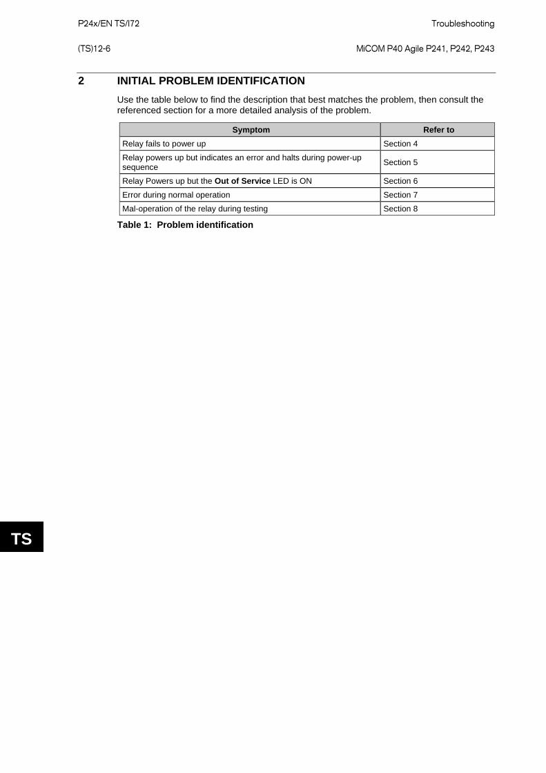
P24x/EN TS/I72
Troubleshooting (TS)12-6 MiCOM P40 Agile P241, P242, P243
TS
2 INITIAL PROBLEM IDENTIFICATION Use the table below to find the description that best matches the problem, then consult the referenced section for a more detailed analysis of the problem.
Symptom Refer to Relay fails to power up Section 4
Relay powers up but indicates an error and halts during power-up sequence Section 5
Relay Powers up but the Out of Service LED is ON Section 6
Error during normal operation Section 7
Mal-operation of the relay during testing Section 8
Table 1: Problem identification
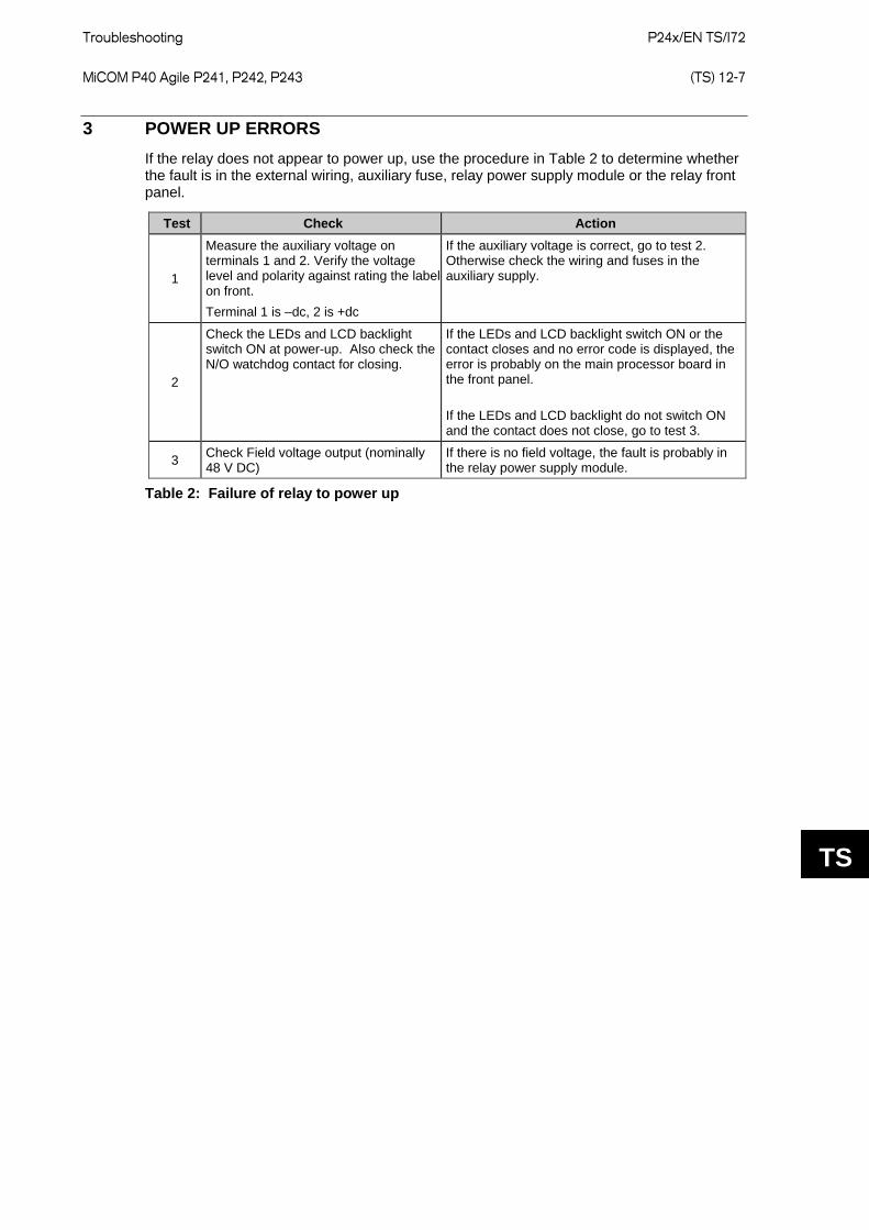
Troubleshooting
P24x/EN TS/I72 MiCOM P40 Agile P241, P242, P243 (TS) 12-7
TS
3 POWER UP ERRORS If the relay does not appear to power up, use the procedure in Table 2 to determine whether the fault is in the external wiring, auxiliary fuse, relay power supply module or the relay front panel.
Test Check Action
1
Measure the auxiliary voltage on terminals 1 and 2. Verify the voltage level and polarity against rating the label on front. Terminal 1 is –dc, 2 is +dc
If the auxiliary voltage is correct, go to test 2. Otherwise check the wiring and fuses in the auxiliary supply.
2
Check the LEDs and LCD backlight switch ON at power-up. Also check the N/O watchdog contact for closing.
If the LEDs and LCD backlight switch ON or the contact closes and no error code is displayed, the error is probably on the main processor board in the front panel. If the LEDs and LCD backlight do not switch ON and the contact does not close, go to test 3.
3 Check Field voltage output (nominally 48 V DC)
If there is no field voltage, the fault is probably in the relay power supply module.
Table 2: Failure of relay to power up
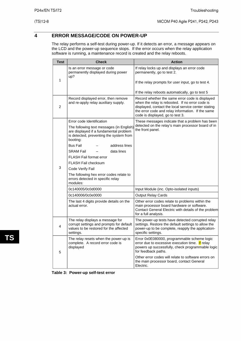
P24x/EN TS/I72
Troubleshooting (TS)12-8 MiCOM P40 Agile P241, P242, P243
TS
4 ERROR MESSAGE/CODE ON POWER-UP The relay performs a self-test during power-up. If it detects an error, a message appears on the LCD and the power-up sequence stops. If the error occurs when the relay application software is running, a maintenance record is created and the relay reboots.
Test Check Action
1
Is an error message or code permanently displayed during power up?
If relay locks up and displays an error code permanently, go to test 2. If the relay prompts for user input, go to test 4. If the relay reboots automatically, go to test 5
2
Record displayed error, then remove and re-apply relay auxiliary supply.
Record whether the same error code is displayed when the relay is rebooted. If no error code is displayed, contact the local service center stating the error code and relay information. If the same code is displayed, go to test 3.
3
Error code Identification The following text messages (in English) are displayed if a fundamental problem is detected, preventing the system from booting: Bus Fail – address lines SRAM Fail – data lines FLASH Fail format error FLASH Fail checksum Code Verify Fail The following hex error codes relate to errors detected in specific relay modules:
These messages indicate that a problem has been detected on the relay’s main processor board of in the front panel.
0c140005/0c0d0000 Input Module (inc. Opto-isolated inputs)
0c140006/0c0e0000 Output Relay Cards
The last 4 digits provide details on the actual error.
Other error codes relate to problems within the main processor board hardware or software. Contact General Electric with details of the problem for a full analysis.
4
The relay displays a message for corrupt settings and prompts for default values to be restored for the affected settings.
The power-up tests have detected corrupted relay settings. Restore the default settings to allow the power-up to be complete, reapply the application-specific settings.
5
The relay resets when the power-up is complete. A record error code is displayed
Error 0x0E080000, programmable scheme logic error due to excessive execution time. If relay powers up successfully, check programmable logic for feedback paths. Other error codes will relate to software errors on the main processor board, contact General Electric.
Table 3: Power-up self-test error
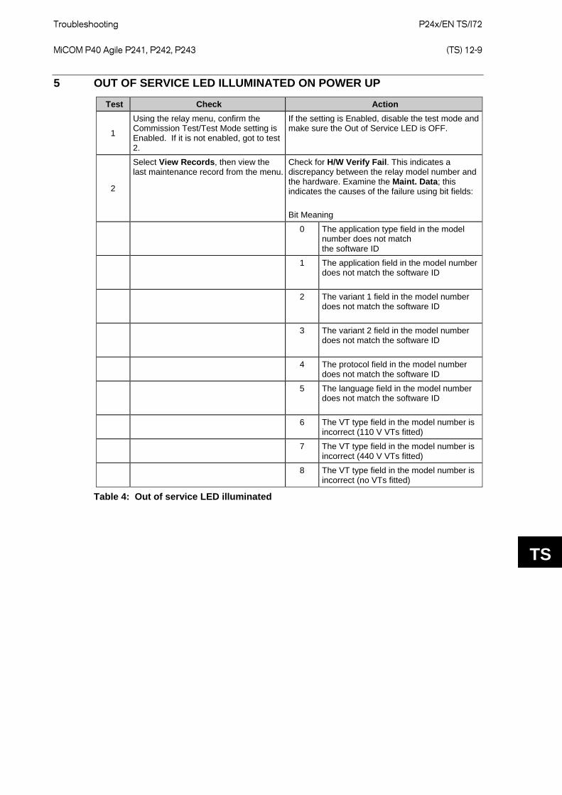
Troubleshooting
P24x/EN TS/I72 MiCOM P40 Agile P241, P242, P243 (TS) 12-9
TS
5 OUT OF SERVICE LED ILLUMINATED ON POWER UP
Test Check Action
1
Using the relay menu, confirm the Commission Test/Test Mode setting is Enabled. If it is not enabled, got to test 2.
If the setting is Enabled, disable the test mode and make sure the Out of Service LED is OFF.
2
Select View Records, then view the last maintenance record from the menu.
Check for H/W Verify Fail. This indicates a discrepancy between the relay model number and the hardware. Examine the Maint. Data; this indicates the causes of the failure using bit fields: Bit Meaning
0 The application type field in the model
number does not match the software ID
1 The application field in the model number
does not match the software ID
2 The variant 1 field in the model number
does not match the software ID
3 The variant 2 field in the model number
does not match the software ID
4 The protocol field in the model number does not match the software ID
5 The language field in the model number
does not match the software ID
6 The VT type field in the model number is incorrect (110 V VTs fitted)
7 The VT type field in the model number is incorrect (440 V VTs fitted)
8 The VT type field in the model number is incorrect (no VTs fitted)
Table 4: Out of service LED illuminated

P24x/EN TS/I72
Troubleshooting (TS)12-10 MiCOM P40 Agile P241, P242, P243
TS
6 ERROR CODE DURING OPERATION The relay performs continuous self-checking. If the relay detects an error it displays an error message, logs a maintenance record and after a 1.6 second delay the relay resets. A permanent problem (for example due to a hardware fault) is usually detected in the power-up sequence, then the relay displays an error code and halts. If the problem was transient, the relay reboots correctly and continues operation. By examining the maintenance record logged, the nature of the detected fault can be determined.
There are also two cases where a maintenance record will be logged due to a detected error where the relay will not reset. These are detection of a failure of either the field voltage or the lithium battery, in these cases the failure is indicated by an alarm message; however the relay will continue to operate.
If the relay detects the field voltage has dropped below threshold, a scheme logic signal is set. This allows the scheme logic to be adapted specifically for this failure (for example if a blocking scheme is being used).
To prevent the relay from issuing an alarm when there is a battery failure, select Date and Time then Battery Alarm then Disabled. The relay can then be used without a battery and no battery alarm message appears.
If there is an RTD board failure, an RTD board fail message appears, the RTD protection is disabled, but the rest of the relay functions normally.

Troubleshooting
P24x/EN TS/I72 MiCOM P40 Agile P241, P242, P243 (TS) 12-11
TS
7 MAL-OPERATION OF THE RELAY DURING TESTING
7.1 Failure of output contacts An apparent failure of the relay output contacts can be caused by the relay configuration; the following tests should be performed to identify the real cause of the failure.
Note: The relay self-tests verify that the coil of the contact has been energized; an error will be displayed if there is a fault in the output relay board.
Test Check Action
1 Is the Out of Service LED ON? If this LED is ON, the relay may be in test mode or
the protection has been disabled due to a hardware verify error (see Table 4).
2 Examine the Contact status in the Commissioning section of the menu.
If the relevant bits of the contact status are operated, go to test 4; if not, go to test 3.
3
Examine the fault record or by use the test port to check the protection element is operating correctly.
If the protection element does not operate check the test is correctly applied. If the protection element operates, check the programmable logic, to make sure the protection element is correctly mapped to the contacts.
4
Using the Commissioning/Test mode function, apply a test pattern to the relevant relay output contacts. Consult the correct external connection diagram and use a continuity tester at the rear of the relay to check the relay output contacts operate.
If the output relay operates, the problem must be in the external wiring to the relay. If the output relay does not operate the output relay contacts may have failed (the self-tests verify that the relay coil is being energized). Ensure the closed resistance is not too high for the continuity tester to detect.
Table 5: Failure of output contacts
7.2 Failure of opto-isolated inputs The opto-isolated inputs are mapped onto the relay internal signals using the programmable scheme logic. If an input does not appear to be recognized by the relay scheme logic use the Commission Tests/Opto Status menu option to check whether the problem is in the opto-isolated input or the mapping of its signal to the scheme logic functions. If the opto-isolated input does appear to be read correctly, examine its mapping in the programmable logic.
If the relay does not correctly read the opto-isolated input state, test the applied signal. Verify the connections to the opto-isolated input using the correct wiring diagram and the nominal voltage settings in the Universal Inputs. menu. In the Universal Inputs. menu select the nominal battery voltage for all opto inputs by selecting one of the five standard ratings in the Global Threshold settings. Select Custom to set each opto input individually to a nominal voltage value. Using a voltmeter, check the voltage on its input terminals is greater than the minimum pick-up level. See chapter P24x/EN/TD for opto pick-up levels. If the signal is correctly applied to the relay, the failure may be on the input card. Depending on which opto-isolated input has failed, the complete analog input module or a separate opto board may need to be replaced. The board in the analog input module cannot be individually replaced without recalibrating the relay.
7.3 Incorrect analog signals The measurements can be configured in primary or secondary to assist. If the analog quantities measured by the relay do not seem correct, use the measurement function of the relay to verify the type of problem. Compare the measured values displayed by the relay with the actual magnitudes at the relay terminals. Check the correct terminals are used (in particular the dual rated CT inputs) and check the CT and VT ratios set on the relay are correct. Use the correct 120 degree displacement of the phase measurements to confirm the inputs are correctly connected.

P24x/EN TS/I72
Troubleshooting (TS)12-12 MiCOM P40 Agile P241, P242, P243
TS
7.4 PSL editor troubleshooting A failure to open a connection could be due to one or more of the following:
• The relay address is not valid (this address is always 1 for the front port). • Password in not valid • Communication Set-up (COM port, Baud rate, or Framing) is not correct • Transaction values are not suitable for the relay or the type of connection • Modem configuration is not valid. Changes may be necessary when using a modem • The connection cable is not wired correctly or broken. See MiCOM S1 Studio connection
configurations • The option switches on any KITZ101/102 this is in use may be incorrectly set
7.4.1 Diagram reconstruction after recover from relay Although a scheme can be extracted from a relay, the facility is provided to recover a scheme if the original file is unobtainable.
A recovered scheme is logically correct but much of the original graphical information is lost. Many signals are drawn in a vertical line down the left side of the canvas. Links are drawn orthogonally using the shortest path from A to B.
Any annotation added to the original diagram such as titles and notes are lost.
Sometimes a gate type does not appear expected. For example, a 1-input AND gate in the original scheme appears as an OR gate when uploaded. Programmable gates with an inputs-to-trigger value of 1 also appear as OR gates.
7.4.2 PSL version check The PSL is saved with a version reference, time stamp and CRC check. This gives a visual check whether the default PSL is in place or whether a new application has been downloaded.
Troubleshooting
P24x/EN TS/I72 MiCOM P40 Agile P241, P242, P243 (TS) 12-13
TS
8 REPAIR AND MODIFICATION PROCEDURE Please follow these 5 steps to return an Automation product to us:
1. Get the Repair and Modification Authorization Form (RMA) • To obtain an electronic version of the RMA form please contact the Contact Centre.
2. Fill in RMA form Fill in only the white part of the form.
Please ensure that all fields marked (M) are completed such as:
• Equipment model • Model No. and Serial No. • Description of failure or modification required (please be specific) • Value for customs (in case the product requires export) • Delivery and invoice addresses • Contact details
3. Send RMA form to your local contact
4. Receive from local service contact, the information required to ship the product Your local service contact will provide you with all the information:
• Pricing details • RMA n° • Repair center address If required, an acceptance of the quote must be delivered before going to next stage.
5. Send the product to the repair center • Address the shipment to the repair center specified by your local contact • Ensure all items are protected by appropriate packaging: anti-static bag and foam
protection • Ensure a copy of the import invoice is attached with the unit being returned • Ensure a copy of the RMA form is attached with the unit being returned • E-mail or fax a copy of the import invoice and airway bill document to your local contact.

P24x/EN TS/I72
Troubleshooting (TS)12-14 MiCOM P40 Agile P241, P242, P243
TS

SCADA Communications
P24x/EN SC/I72 MiCOM P40 Agile P241, P242, P243 (SC) 13-1
SC
SCADA COMMUNICATIONS

P24x/EN SC/I72
SCADA Communications (SC) 13-2 MiCOM P40 Agile P241, P242, P243
SC
SCADA Communications
P24x/EN SC/I72 MiCOM P40 Agile P241, P242, P243 (SC) 13-3
SC
CONTENTS
1 INTRODUCTION 7
2 REAR PORT INFORMATION AND CONNECTION ADVICE – EIA(RS)485 PROTOCOLS 8
2.1 Rear communication port EIA(RS)485 interface 8
2.2 EIA(RS)485 bus 8
2.2.1 Bus termination 8
2.2.2 Bus connections & topologies 8
2.2.3 Biasing 8
2.2.4 Courier communication 9
2.2.5 MODBUS communication 12
2.2.6 IEC 60870-5 CS 103 communication 13
2.3 Second rear communication port 15
3 COURIER INTERFACE 18
3.1 Courier protocol 18
3.2 Front courier port 18
3.3 Supported command set 19
3.4 Relay courier database 19
3.5 Setting changes 20
3.5.1 Method 1 20
3.5.2 Method 2 20
3.5.3 Relay settings 20
3.5.4 Setting transfer mode 20
3.6 Event extraction 21
3.6.1 Automatic event extraction 21
3.6.2 Event types 21
3.6.3 Event format 21
3.6.4 Manual event record extraction 22
3.7 Disturbance record extraction 22
3.8 Programmable scheme logic settings 22
4 MODBUS INTERFACE 24
4.1 Serial interface 24
4.1.1 Character framing 24
4.1.2 Maximum MODBUS query and response frame size 24
4.1.3 User configurable communications parameters 24
4.2 Supported MODBUS query functions 24
4.3 MODBUS response code interpretation 25
4.4 Maximum query and response parameters 25
4.5 Register mapping 26

P24x/EN SC/I72
SCADA Communications (SC) 13-4 MiCOM P40 Agile P241, P242, P243
SC
4.5.1 Conventions 26
4.5.1.1 Memory pages 26
4.5.1.2 MODBUS register identification 26
4.6 Register map 27
4.7 Measurement values 28
4.8 Binary status information 32
4.9 Measurement and binary status 3x register sets 34
4.10 Controls 35
4.11 Event extraction 35
4.11.1 Manual extraction procedure 36
4.11.2 Automatic extraction procedure 36
4.11.3 Record data 37
4.11.4 Event record deletion 40
4.11.5 Event record support 40
4.12 Disturbance record extraction 40
4.12.1 Interface registers 41
4.12.2 Extraction procedure 42
4.12.2.1 Manual extraction procedure 43
4.12.2.2 Automatic extraction procedure - option 1 44
4.12.2.3 Automatic extraction procedure - option 2 45
4.12.2.4 Extracting the disturbance data 47
4.12.3 Storage of extracted data 49
4.12.3.1 Storing the configuration file 49
4.12.3.2 Storing the binary data file 49
4.12.4 Disturbance record deletion 49
4.13 Setting changes 49
4.13.1 Password protection 49
4.13.2 Control and support settings 50
4.13.2.1 Time synchronization 50
4.13.3 Disturbance recorder configuration settings 50
4.13.4 Protection settings 50
4.13.5 Scratchpad management 51
4.14 Register data types 51
4.15 Numeric setting (data types G2 & G35) 51
4.16 Date and time format (data type G12) 52
4.17 Power and energy measurement data formats (G29 & G125) 53
4.17.1 Data type G29 53
4.17.2 Data type G125 54
5 IEC 60870-5-103 INTERFACE 55
5.1 Physical connection and link layer 55
5.2 Initialization 55
5.3 Time synchronization 55
SCADA Communications
P24x/EN SC/I72 MiCOM P40 Agile P241, P242, P243 (SC) 13-5
SC
5.4 Spontaneous events 55
5.5 General interrogation 56
5.6 Cyclic measurements 56
5.7 Commands 56
5.8 Test mode 56
5.9 Disturbance records 56
5.10 Blocking of monitor direction 56
6 IEC 61850 ETHERNET INTERFACE 57
6.1 Introduction 57
6.2 What is IEC 61850? 57
6.2.1 Interoperability 57
6.2.2 The data model 57
6.3 IEC 61850 in MiCOM relays 59
6.3.1 Capability 59
6.3.2 IEC 61850 configuration 60
6.3.2.1 Configuration banks 61
6.3.2.2 Network connectivity 61
6.4 The data model of MiCOM relays 61
6.5 The communication services of MiCOM relays 61
6.6 Peer-to-peer (GSE) communications 62
6.6.1 Scope 62
6.6.2 IEC 61850 GOOSE configuration 62
6.7 Ethernet functionality 62
6.7.1 Ethernet disconnection 63
6.7.2 Redundant Ethernet communication ports 63
6.7.3 Loss of power 63
7 SECOND REAR COMMUNICATIONS PORT (COURIER) 64
7.1 Courier protocol 64
7.2 Event extraction 64
7.3 Disturbance record extraction 64
7.4 Connection to the second rear port 64
8 SK5 PORT CONNECTION 66
FIGURES Figure 1: EIA(RS)485 bus connection arrangements 9
Figure 2: Remote communication connection arrangements 10
Figure 3: Second rear port K-Bus application 16
Figure 4: Second rear port EIA(RS)485 example 17
Figure 5: Second rear port EIA(RS)232 example 17
Figure 6: Automatic event extraction procedure 37
P24x/EN SC/I72
SCADA Communications (SC) 13-6 MiCOM P40 Agile P241, P242, P243
SC
Figure 7: Manual selection of a disturbance record 43
Figure 8: Automatic selection of a disturbance - option 1 44
Figure 9: Automatic selection of a disturbance - option 2 46
Figure 10: Extracting the COMTRADE configuration file 47
Figure 11: Extracting the COMTRADE binary data file 48
Figure 12: Data model layers in IEC 61850 58
TABLES Table 1: MODBUS query functions supported by the product 25
Table 2: MODBUS response code interpretation 25
Table 3: Maximum query and response parameters for supported queries 26
Table 4: MODBUS "memory" pages reference and application 26
Table 5: Measurement data available in the P240 product range 32
Table 6: Binary status information available in the P240 product range 34
Table 7: Event record extraction registers 38
Table 8: Maintenance record types 39
Table 9: Event record 3x registers 40
Table 10: Disturbance record extraction registers 41
Table 11: Disturbance record status register (3x934) values 42
Table 12: Example of numeric settings 51
Table 13: G12 date & time data type structure 52
Table 14: Available physical links and their corresponding valid protocols 64
Table 15: EIA (RS)232 pin designation 65
Table 16: EIA (RS)485 pin designation 65

SCADA Communications
P24x/EN SC/I72 MiCOM P40 Agile P241, P242, P243 (SC) 13-7
SC
1 INTRODUCTION This chapter describes the remote interfaces of the MiCOM relay in enough detail to allow integration in a substation communication network. As outlined in earlier chapters, the relay supports a choice of one of four protocols through the rear communication interface, selected using the model number when ordering. This is in addition to the front serial interface and 2nd rear communications port, which supports the Courier protocol only.
The rear EIA(RS)485 interface is isolated and is suitable for permanent connection whichever protocol is selected. The advantage of this type of connection is that up to 32 relays can be daisy chained together using a simple twisted pair electrical connection.
For each of the protocol options, the supported functions and commands are listed with the database definition. The operation of standard procedures such as extraction of event, fault and disturbance records, or setting changes, is also described.
The descriptions in this chapter do not aim to fully describe the protocol in detail. Refer to the relevant documentation protocol for this information. This chapter describes the specific implementation of the protocol in the relay.
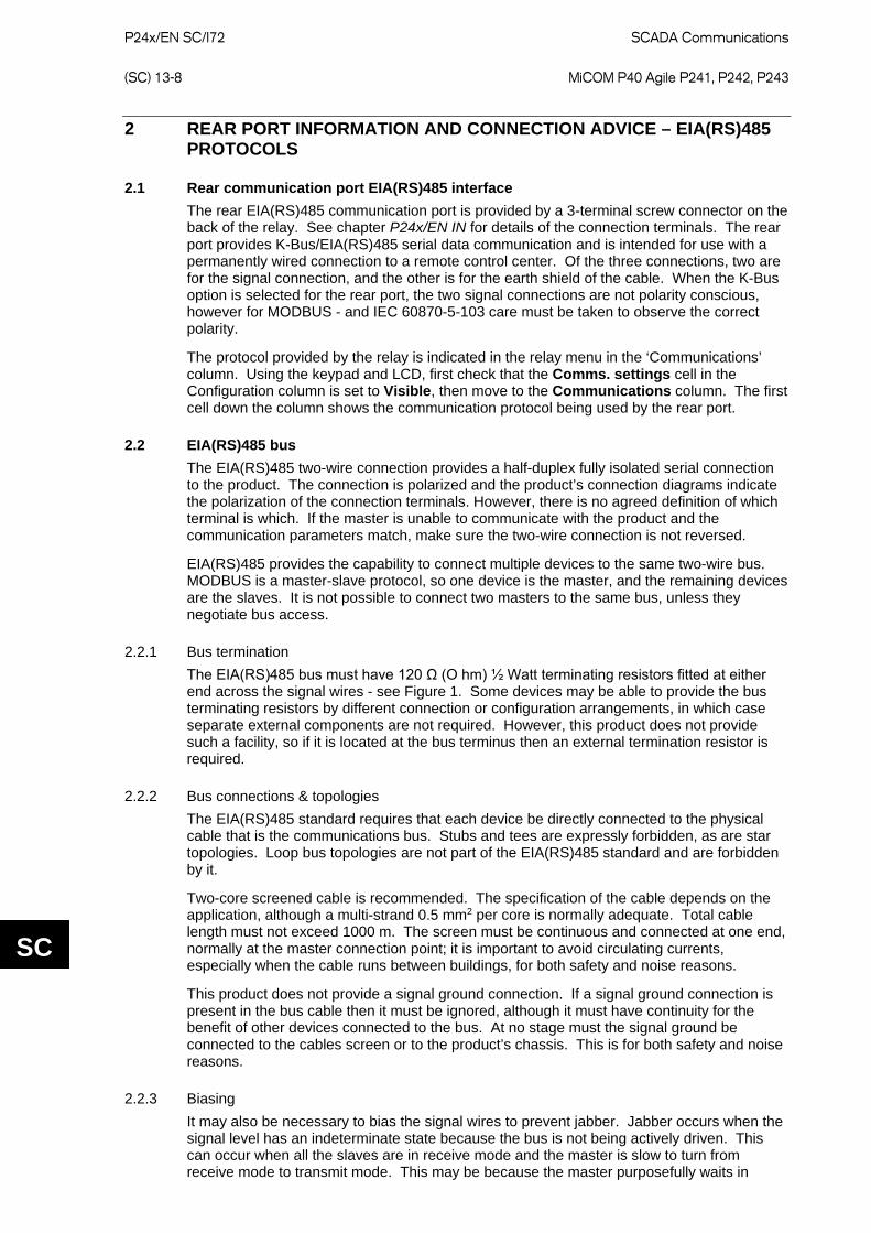
P24x/EN SC/I72
SCADA Communications (SC) 13-8 MiCOM P40 Agile P241, P242, P243
SC
2 REAR PORT INFORMATION AND CONNECTION ADVICE – EIA(RS)485 PROTOCOLS
2.1 Rear communication port EIA(RS)485 interface The rear EIA(RS)485 communication port is provided by a 3-terminal screw connector on the back of the relay. See chapter P24x/EN IN for details of the connection terminals. The rear port provides K-Bus/EIA(RS)485 serial data communication and is intended for use with a permanently wired connection to a remote control center. Of the three connections, two are for the signal connection, and the other is for the earth shield of the cable. When the K-Bus option is selected for the rear port, the two signal connections are not polarity conscious, however for MODBUS - and IEC 60870-5-103 care must be taken to observe the correct polarity.
The protocol provided by the relay is indicated in the relay menu in the ‘Communications’ column. Using the keypad and LCD, first check that the Comms. settings cell in the Configuration column is set to Visible, then move to the Communications column. The first cell down the column shows the communication protocol being used by the rear port.
2.2 EIA(RS)485 bus The EIA(RS)485 two-wire connection provides a half-duplex fully isolated serial connection to the product. The connection is polarized and the product’s connection diagrams indicate the polarization of the connection terminals. However, there is no agreed definition of which terminal is which. If the master is unable to communicate with the product and the communication parameters match, make sure the two-wire connection is not reversed.
EIA(RS)485 provides the capability to connect multiple devices to the same two-wire bus. MODBUS is a master-slave protocol, so one device is the master, and the remaining devices are the slaves. It is not possible to connect two masters to the same bus, unless they negotiate bus access.
2.2.1 Bus termination The EIA(RS)485 bus must have 120 Ω (O hm) ½ Watt terminating resistors fitted at either end across the signal wires - see Figure 1. Some devices may be able to provide the bus terminating resistors by different connection or configuration arrangements, in which case separate external components are not required. However, this product does not provide such a facility, so if it is located at the bus terminus then an external termination resistor is required.
2.2.2 Bus connections & topologies The EIA(RS)485 standard requires that each device be directly connected to the physical cable that is the communications bus. Stubs and tees are expressly forbidden, as are star topologies. Loop bus topologies are not part of the EIA(RS)485 standard and are forbidden by it.
Two-core screened cable is recommended. The specification of the cable depends on the application, although a multi-strand 0.5 mm2 per core is normally adequate. Total cable length must not exceed 1000 m. The screen must be continuous and connected at one end, normally at the master connection point; it is important to avoid circulating currents, especially when the cable runs between buildings, for both safety and noise reasons.
This product does not provide a signal ground connection. If a signal ground connection is present in the bus cable then it must be ignored, although it must have continuity for the benefit of other devices connected to the bus. At no stage must the signal ground be connected to the cables screen or to the product’s chassis. This is for both safety and noise reasons.
2.2.3 Biasing It may also be necessary to bias the signal wires to prevent jabber. Jabber occurs when the signal level has an indeterminate state because the bus is not being actively driven. This can occur when all the slaves are in receive mode and the master is slow to turn from receive mode to transmit mode. This may be because the master purposefully waits in
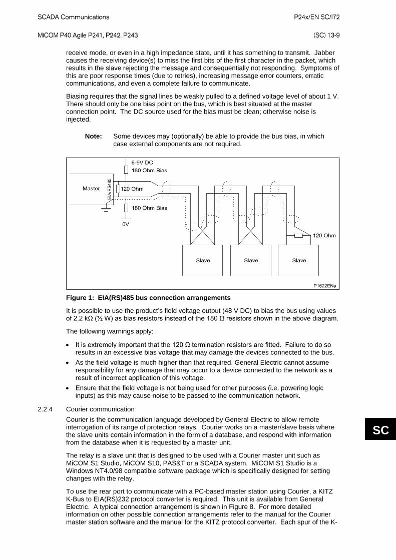
SCADA Communications
P24x/EN SC/I72 MiCOM P40 Agile P241, P242, P243 (SC) 13-9
SC
receive mode, or even in a high impedance state, until it has something to transmit. Jabber causes the receiving device(s) to miss the first bits of the first character in the packet, which results in the slave rejecting the message and consequentially not responding. Symptoms of this are poor response times (due to retries), increasing message error counters, erratic communications, and even a complete failure to communicate.
Biasing requires that the signal lines be weakly pulled to a defined voltage level of about 1 V. There should only be one bias point on the bus, which is best situated at the master connection point. The DC source used for the bias must be clean; otherwise noise is injected.
Note: Some devices may (optionally) be able to provide the bus bias, in which case external components are not required.
Figure 1: EIA(RS)485 bus connection arrangements
It is possible to use the product’s field voltage output (48 V DC) to bias the bus using values of 2.2 kΩ (½ W) as bias resistors instead of the 180 Ω resistors shown in the above diagram.
The following warnings apply:
• It is extremely important that the 120 Ω termination resistors are fitted. Failure to do so results in an excessive bias voltage that may damage the devices connected to the bus.
• As the field voltage is much higher than that required, General Electric cannot assume responsibility for any damage that may occur to a device connected to the network as a result of incorrect application of this voltage.
• Ensure that the field voltage is not being used for other purposes (i.e. powering logic inputs) as this may cause noise to be passed to the communication network.
2.2.4 Courier communication Courier is the communication language developed by General Electric to allow remote interrogation of its range of protection relays. Courier works on a master/slave basis where the slave units contain information in the form of a database, and respond with information from the database when it is requested by a master unit.
The relay is a slave unit that is designed to be used with a Courier master unit such as MiCOM S1 Studio, MiCOM S10, PAS&T or a SCADA system. MiCOM S1 Studio is a Windows NT4.0/98 compatible software package which is specifically designed for setting changes with the relay.
To use the rear port to communicate with a PC-based master station using Courier, a KITZ K-Bus to EIA(RS)232 protocol converter is required. This unit is available from General Electric. A typical connection arrangement is shown in Figure 8. For more detailed information on other possible connection arrangements refer to the manual for the Courier master station software and the manual for the KITZ protocol converter. Each spur of the K-
P24x/EN SC/I72
SCADA Communications (SC) 13-10 MiCOM P40 Agile P241, P242, P243
SC
Bus twisted pair wiring can be up to 1000 m in length and have up to 32 relays connected to it.
P0109ENe
Figure 2: Remote communication connection arrangements
Having made the physical connection to the relay, the relay’s communication settings must be configured. To do this use the keypad and LCD user interface. In the relay menu firstly check that the Comms. settings cell in the Configuration column is set to Visible, then move to the Communications column. Only two settings apply to the rear port using Courier, the relay’s address and the inactivity timer. Synchronous communication is used at a fixed baud rate of 64 kbits/s.
Move down the Communications column from the column heading to the first cell down which indicates the communication protocol:
RP1 Protocol Courier
The next cell down the column controls the address of the relay:

SCADA Communications
P24x/EN SC/I72 MiCOM P40 Agile P241, P242, P243 (SC) 13-11
SC
RP1 Address 1
Since up to 32 relays can be connected to one K-Bus spur, as indicated in Figure 8, it is necessary for each relay to have a unique address so that messages from the master control station are accepted by one relay only. Courier uses an integer number between 0 and 254 for the relay address that is set with this cell. It is important that no two relays have the same Courier address. The Courier address is then used by the master station to communicate with the relay.
The next cell down controls the inactivity timer:
RP1 Inactiv timer 10.00 mins.
The inactivity timer controls how long the relay waits without receiving any messages on the rear port before it reverts to its default state, including revoking any password access that was enabled. For the rear port this can be set between 1 and 30 minutes.
The next cell down the column controls the physical media used for the communication:
RP1 Physical link Copper
The default setting is to select the copper electrical EIA(RS)485 connection. If the optional fiber optic connectors are fitted to the relay, then this setting can be changed to Fiber optic. This cell is also invisible if second rear comms. port is fitted as it is mutually exclusive with the fiber optic connectors.
As an alternative to running Courier over K-Bus, Courier over EIA(RS)485 may be selected. The next cell down indicates the status of the hardware, e.g.:
RP1 Card status EIA(RS)232 OK
The next cell allows for selection of the port configuration:
RP1 Port config. EIA(RS)232
The port can be configured for EIA(RS)485 or K-Bus.
In the case of EIA(RS)485 the next cell selects the communication mode:
RP1 Comms. Mode IEC 60870 FT1.2
The choice is either IEC 60870 FT1.2 for normal operation with 11-bit modems, or 10-bit no parity.
In the case of EIA(RS)485 the next cell down controls the baud rate. For K-Bus the baud rate is fixed at 64kbit/second between the relay and the KITZ interface at the end of the relay spur.
RP1 Baud rate 19200
P24x/EN SC/I72
SCADA Communications (SC) 13-12 MiCOM P40 Agile P241, P242, P243
SC
Courier communications is asynchronous. Three baud rates are supported by the relay, ‘9600 bits/s’, ‘19200 bits/s’ and ‘38400 bits/s’,
Protection and disturbance recorder settings that are modified using an on-line editor such as PAS&T must be confirmed with a write to the Save changes cell of the Configuration column. Off-line editors such as MiCOM S1 Studio do not require this action for the setting changes to take effect.
2.2.5 MODBUS communication MODBUS is a master/slave communication protocol that can be used for network control. In a similar fashion to Courier, the system works by the master device initiating all actions and the slave devices, (the relays), responding to the master by supplying the requested data or by taking the requested action. MODBUS communication is achieved via a twisted pair connection to the rear port and can be used over a distance of 1000 m with up to 32 slave devices.
To use the rear port with MODBUS communication, the relay’s communication settings must be configured. To do this use the keypad and LCD user interface. In the relay menu firstly check that the Comms. settings cell in the Configuration column is set to Visible, then move to the Communications column. Four settings apply to the rear port using MODBUS that are described below. Move down the Communications column from the column heading to the first cell down that indicates the communication protocol:
RP1 Protocol MODBUS
The next cell down controls the MODBUS address of the relay:
RP1 MODBUS address 23
Up to 32 relays can be connected to one MODBUS spur, and therefore it is necessary for each relay to have a unique address so that messages from the master control station are accepted by one relay only. MODBUS uses an integer number between 1 and 247 for the relay address. It is important that no two relays have the same MODBUS address. The MODBUS address is then used by the master station to communicate with the relay.
The next cell down controls the inactivity timer:
RP1 Inactiv timer 10.00 mins.
The inactivity timer controls how long the relay waits without receiving any messages on the rear port before it reverts to its default state, including revoking any password access that was enabled. For the rear port this can be set between 1 and 30 minutes.
The next cell down the column controls the baud rate to be used:
RP1 Baud rate 9600 bits/s
MODBUS communication is asynchronous. Three baud rates are supported by the relay, ‘9600 bits/s’, ‘19200 bits/s’ and ‘38400 bits/s’. It is important that whatever baud rate is selected on the relay is the same as that set on the MODBUS master station.
The next cell down controls the parity format used in the data frames:
SCADA Communications
P24x/EN SC/I72 MiCOM P40 Agile P241, P242, P243 (SC) 13-13
SC
RP1 Parity None
The parity can be set to be one of ‘None’, ‘Odd’ or ‘Even’. It is important that whatever parity format is selected on the relay is the same as that set on the MODBUS master station.
The next cell down the column controls the physical media used for the communication:
RP1 Physical link Copper
The default setting is to select the copper electrical EIA(RS)485 connection. If the optional fiber optic connectors are fitted to the relay, then this setting can be changed to Fiber optic. This cell is also invisible if second rear comms. port is fitted as it is mutually exclusive with the fiber optic connectors.
The next cell down controls the format of the Date/Time (software 30 or later):
MODBUS IEC time standard
The format can be selected to either ‘Standard’ (as per IEC 60870-5-4 ‘Binary Time 2 a’), the default, or to ‘Reverse’ for compatibility with MICOM product ranges. For further information see Data and time format in section 4.16.
2.2.6 IEC 60870-5 CS 103 communication The IEC specification IEC 60870-5-103: Telecontrol Equipment and Systems, Part 5: Transmission Protocols Section 103 defines the use of standards IEC 60870-5-1 to IEC 60870-5-5 to perform communication with protection equipment. The standard configuration for the IEC 60870-5-103 protocol is to use a twisted pair connection over distances up to 1000 m. As an option for IEC 60870-5-103, the rear port can be specified to use a fiber optic connection for direct connection to a master station. The relay operates as a slave in the system, responding to commands from a master station. The method of communication uses standardized messages which are based on the VDEW communication protocol.
To use the rear port with IEC 60870-5-103 communication, the relay’s communication settings must be configured. To do this use the keypad and LCD user interface. In the relay menu first check that the Comms. settings cell in the Configuration column is set to Visible, then move to the Communications column. Four settings apply to the rear port using IEC 60870-5-103 that are described below.
Move down the Communications column from the column heading to the first cell that indicates the communication protocol:
RP1 Protocol IEC 60870-5-103
The next cell down controls the IEC 60870-5-103 address of the relay:
RP1 address 162
P24x/EN SC/I72
SCADA Communications (SC) 13-14 MiCOM P40 Agile P241, P242, P243
SC
Up to 32 relays can be connected to one IEC 60870-5-103 spur, and therefore it is necessary for each relay to have a unique address so that messages from the master control station are accepted by one relay only. IEC 60870-5-103 uses an integer number between 0 and 254 for the relay address. It is important that no two relays have the same IEC 60870-5-103 address. The IEC 60870-5-103 address is then used by the master station to communicate with the relay.
The next cell down the column controls the baud rate to be used:
RP1 Baud rate 9600 bits/s
IEC 60870-5-103 communication is asynchronous. Two baud rates are supported by the relay, ‘9600 bits/s’ and ‘19200 bits/s’. It is important that whatever baud rate is selected on the relay is the same as that set on the IEC 60870-5-103 master station.
The next cell down controls the period between IEC 60870-5-103 measurements:
RP1 Meas. Period 30.00 s
The IEC 60870-5-103 protocol allows the relay to supply measurements at regular intervals. The interval between measurements is controlled by this cell, and can be set between 1 and 60 seconds.
The following cell is not currently used but is available for future expansion:
RP1 Inactiv timer
The next cell down the column controls the physical media used for the communication:
RP1 Physical link Copper
The default setting is to select the copper electrical EIA(RS)485 connection. If the optional fiber optic connectors are fitted to the relay, then this setting can be changed to Fiber optic. This cell is also invisible if second rear comms. port is fitted as it is mutually exclusive with the fiber optic connectors.
The next cell down can be used for monitor or command blocking:
RP1 CS103 Blocking
There are three settings associated with this cell; these are:
• Disabled No blocking selected. • Monitor Blocking When the monitor blocking DDB Signal is active high, either
by energizing an opto input or control input, reading of the status information and disturbance records is not permitted. When in this mode the relay returns a Termination of general interrogation message to the master station.
• Command Blocking When the command blocking DDB signal is active high, either by energizing an opto input or control input, all remote commands are ignored (such as CB Trip/Close and change setting group.). When in this mode the relay returns a negative acknowledgement of command message to the master station.
SCADA Communications
P24x/EN SC/I72 MiCOM P40 Agile P241, P242, P243 (SC) 13-15
SC
2.3 Second rear communication port For relays with Courier, MODBUS, IEC 60870-5-103 or DNP3.0 protocol on the first rear communications port there is the hardware option of a second rear communications port, which runs the Courier language. This can be used over one of three physical links: twisted pair K-Bus (non-polarity sensitive), twisted pair EIA(RS)485 (connection polarity sensitive) or EIA(RS)232.
The settings for this port are located immediately below the ones for the first port as described in the Introduction chapter, P24x/EN IT. Move down the settings until the following sub heading is displayed:
Rear port2 (RP2)
The next cell down indicates the language, which is fixed at Courier for RP2:
RP2 Protocol Courier
The next cell down indicates the status of the hardware, e.g.:
RP2 Card status EIA(RS)232 OK
The next cell allows for selection of the port configuration:
RP2 Port config. EIA(RS)232
The port can be configured for EIA(RS)232, EIA(RS)485 or K-Bus.
In the case of EIA(RS)232 and EIA(RS)485 the next cell selects the communication mode:
RP2 Comms. mode IEC 60870 FT1.2
The choice is either IEC 60870 FT1.2 for normal operation with 11-bit modems, or 10-bit no parity.
The next cell down controls the comms. port address:
RP2 Address 255
Up to 32 relays can be connected to one K-Bus spur, as shown in Figure 9, it is necessary for each relay to have a unique address so that messages from the master control station are accepted by one relay only. Courier uses an integer number between 0 and 254 for the relay address that is set with this cell. It is important that no two relays have the same Courier address. The Courier address is then used by the master station to communicate with the relay.
The next cell down controls the inactivity timer:
RP2 Inactivity timer 15 mins.
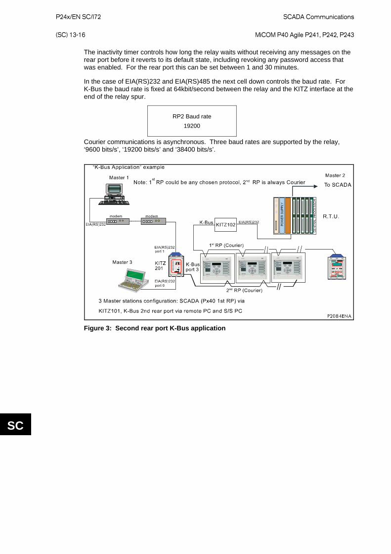
P24x/EN SC/I72
SCADA Communications (SC) 13-16 MiCOM P40 Agile P241, P242, P243
SC
The inactivity timer controls how long the relay waits without receiving any messages on the rear port before it reverts to its default state, including revoking any password access that was enabled. For the rear port this can be set between 1 and 30 minutes.
In the case of EIA(RS)232 and EIA(RS)485 the next cell down controls the baud rate. For K-Bus the baud rate is fixed at 64kbit/second between the relay and the KITZ interface at the end of the relay spur.
RP2 Baud rate 19200
Courier communications is asynchronous. Three baud rates are supported by the relay, ‘9600 bits/s’, ‘19200 bits/s’ and ‘38400 bits/s’.
Figure 3: Second rear port K-Bus application
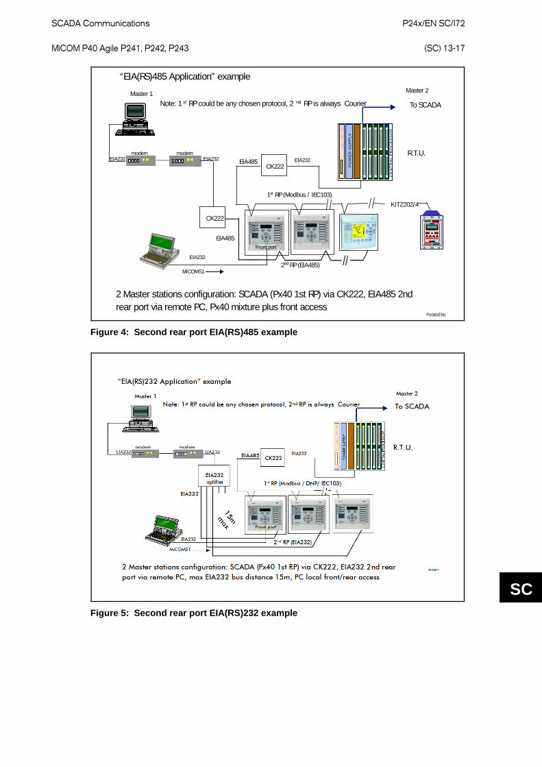
SCADA Communications
P24x/EN SC/I72 MiCOM P40 Agile P241, P242, P243 (SC) 13-17
SC
2 Master stations configuration: SCADA (Px40 1st RP) via CK222, EIA485 2ndrear port via remote PC, Px40 mixture plus front access
2nd RP (EIA485)
1st RP (Modbus / IEC103)
modem modemEIA232 EIA232
EIA232
Master 1 Master 2
EIA485
PO
WE
R S
UP
PLY
CE
NT
RA
L P
RO
CE
SS
OR
R.T.U.
To SCADA
CK222
Front port
MiCOMS1
EIA232
Note: 1st RP could be any chosen protocol, 2 nd RP is always Courier
CK222
KITZ202/4
EIA485
“EIA(RS)485 Application” example
P2085ENc
Figure 4: Second rear port EIA(RS)485 example
Figure 5: Second rear port EIA(RS)232 example
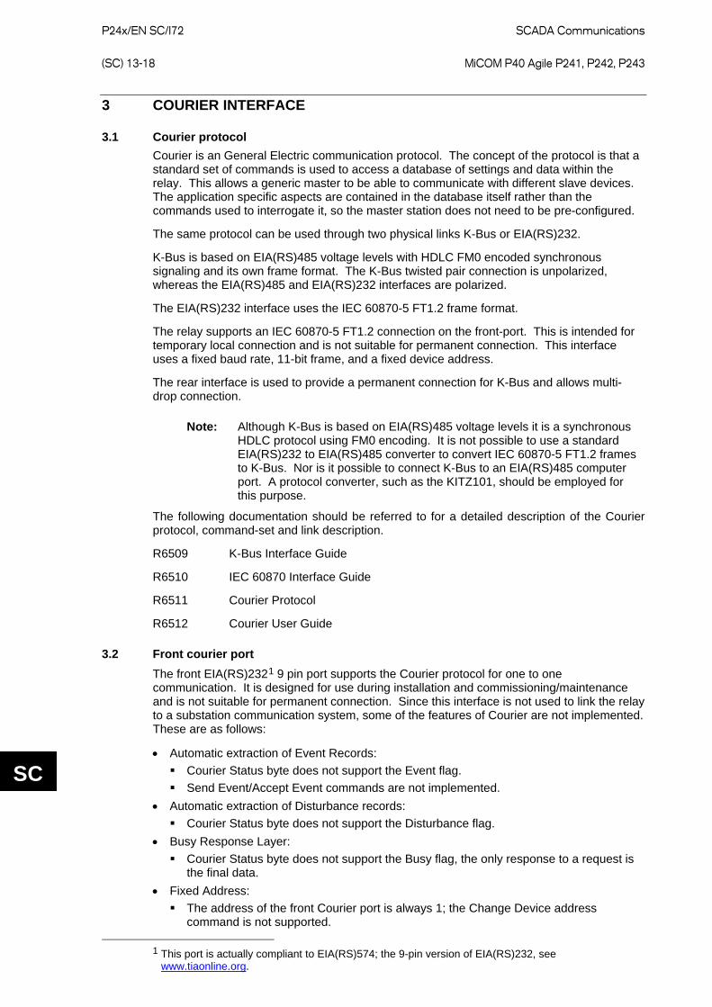
P24x/EN SC/I72
SCADA Communications (SC) 13-18 MiCOM P40 Agile P241, P242, P243
SC
3 COURIER INTERFACE
3.1 Courier protocol Courier is an General Electric communication protocol. The concept of the protocol is that a standard set of commands is used to access a database of settings and data within the relay. This allows a generic master to be able to communicate with different slave devices. The application specific aspects are contained in the database itself rather than the commands used to interrogate it, so the master station does not need to be pre-configured.
The same protocol can be used through two physical links K-Bus or EIA(RS)232.
K-Bus is based on EIA(RS)485 voltage levels with HDLC FM0 encoded synchronous signaling and its own frame format. The K-Bus twisted pair connection is unpolarized, whereas the EIA(RS)485 and EIA(RS)232 interfaces are polarized.
The EIA(RS)232 interface uses the IEC 60870-5 FT1.2 frame format.
The relay supports an IEC 60870-5 FT1.2 connection on the front-port. This is intended for temporary local connection and is not suitable for permanent connection. This interface uses a fixed baud rate, 11-bit frame, and a fixed device address.
The rear interface is used to provide a permanent connection for K-Bus and allows multi-drop connection.
Note: Although K-Bus is based on EIA(RS)485 voltage levels it is a synchronous HDLC protocol using FM0 encoding. It is not possible to use a standard EIA(RS)232 to EIA(RS)485 converter to convert IEC 60870-5 FT1.2 frames to K-Bus. Nor is it possible to connect K-Bus to an EIA(RS)485 computer port. A protocol converter, such as the KITZ101, should be employed for this purpose.
The following documentation should be referred to for a detailed description of the Courier protocol, command-set and link description.
R6509 K-Bus Interface Guide
R6510 IEC 60870 Interface Guide
R6511 Courier Protocol
R6512 Courier User Guide
3.2 Front courier port The front EIA(RS)2321 9 pin port supports the Courier protocol for one to one communication. It is designed for use during installation and commissioning/maintenance and is not suitable for permanent connection. Since this interface is not used to link the relay to a substation communication system, some of the features of Courier are not implemented. These are as follows:
• Automatic extraction of Event Records: Courier Status byte does not support the Event flag. Send Event/Accept Event commands are not implemented.
• Automatic extraction of Disturbance records: Courier Status byte does not support the Disturbance flag.
• Busy Response Layer: Courier Status byte does not support the Busy flag, the only response to a request is
the final data. • Fixed Address: The address of the front Courier port is always 1; the Change Device address
command is not supported.
1 This port is actually compliant to EIA(RS)574; the 9-pin version of EIA(RS)232, see www.tiaonline.org.

SCADA Communications
P24x/EN SC/I72 MiCOM P40 Agile P241, P242, P243 (SC) 13-19
SC
• Fixed Baud Rate: 19200 bps.
Note: Although automatic extraction of event and disturbance records is not supported it is possible to manually access this data through the front port.
3.3 Supported command set The following Courier commands are supported by the relay:
• Protocol Layer Reset Remote Link Poll Status Poll Buffer*
• Low Level Commands Send Event* Accept Event* Send Block Store Block Identifier Store Block Footer
• Menu Browsing Get Column Headings Get Column Text Get Column Values Get Strings Get Text Get Value Get Column Setting Limits
• Setting Changes Enter Setting Mode Preload Setting Abort Setting Execute Setting Reset Menu Cell Set Value
• Control Commands Select Setting Group Change Device Address* Set Real Time
Note: Commands indicated with an * are not supported via the front Courier port.
3.4 Relay courier database The Courier database is two-dimensional. Each cell in the database is referenced by a row and column address. Both the column and the row can take a range from 0 to 255. Addresses in the database are specified as hexadecimal values, for example, 0A02 is column 0A (10 decimal) row 02. Associated settings or data are part of the same column. Row zero of the column has a text string to identify the contents of the column and to act as a column heading.
The Relay Menu Database contains the complete database definition for the relay and is available on request. For each cell location the following information is stated:
• Cell Text • Cell Datatype • Cell value

P24x/EN SC/I72
SCADA Communications (SC) 13-20 MiCOM P40 Agile P241, P242, P243
SC
• Whether the cell is settable, if so • Minimum value • Maximum value • Step size • Password Level required to allow setting changes • String information (for Indexed String or Binary flag cells)
3.5 Setting changes (See R6512, Courier User Guide - Chapter 9)
Courier provides two mechanisms for making setting changes, both of these are supported by the relay. Either method can be used for editing any of the settings within the relay database.
3.5.1 Method 1 This uses a combination of three commands to perform a settings change:
• Enter Setting Mode - Checks that the cell is settable and returns the limits. • Pre-load Setting - Places a new value to the cell, this value is echoed to
ensure that setting corruption has not taken place, the validity of the setting is not checked by this action.
• Execute Setting - Confirms the setting change, if the change is valid then a positive response is returned. If the setting change fails then an error response is returned.
• Abort Setting - This command can be used to abandon the setting change.
This is the most secure method and is ideally suited to on-line editors as the setting limits are taken from the relay before the setting change is made. However, this method can be slow if many settings are being changed as three commands are required for each change.
3.5.2 Method 2 The Set Value command can be used to directly change a setting, the response to this command is either a positive confirm or an error code to indicate the nature of a failure. This command can be used to implement a setting more rapidly then the previous method, however the limits are not extracted from the relay. This method is most suitable for off-line setting editors such as MiCOM S1 Studio, or for the issuing of pre-configured (SCADA) control commands.
3.5.3 Relay settings There are three categories of settings within the relay database:
• Control and support • Disturbance recorder • Protection settings group Setting changes made to the control and support settings are implemented immediately and stored in non-volatile memory. Changes made to either the Disturbance recorder settings or the Protection Settings Groups are stored in a ‘scratchpad’ memory and are not immediately implemented by the relay.
To action setting changes stored in the scratchpad the Save Changes cell in the Configuration column must be written to. This allows the changes to either be confirmed and stored in non-volatile memory, or the setting changes to be aborted.
3.5.4 Setting transfer mode If it is necessary to transfer all of the relay settings to or from the relay a cell within the Communication System Data column can be used. This cell (location BF03) when set to 1 makes all of the relay settings visible. Any setting changes made, with the relay set in this mode, are stored in scratchpad memory (including control and support settings). When the
SCADA Communications
P24x/EN SC/I72 MiCOM P40 Agile P241, P242, P243 (SC) 13-21
SC
value of BF03 is set back to 0 any setting changes are verified and stored in non-volatile memory.
3.6 Event extraction Events can be extracted either automatically (rear port only) or manually (either Courier port). For automatic extraction all events are extracted in sequential order using the standard Courier event mechanism, this includes fault/maintenance data if appropriate. The manual approach allows the user to select events, faults, or maintenance data at random from the stored records.
3.6.1 Automatic event extraction (See Chapter 7 Courier User Guide, publication R6512).
This method is intended for continuous extraction of event and fault information as it is produced. It is only supported via the rear Courier port.
When new event information is created the Event bit is set within the Status byte, this indicates to the Master device that event information is available. The oldest, unextracted event can be extracted from the relay using the Send Event command. The relay responds with the event data, which is either a Courier Type 0 or Type 3 event. The Type 3 event is used for fault records and maintenance records.
Once an event has been extracted from the relay, the Accept Event can be used to confirm that the event has been successfully extracted. If all events have been extracted then the event bit is reset, if there are more events still to be extracted the next event can be accessed using the Send Event command as before.
3.6.2 Event types Events are created by the relay under the following circumstances:
• Change of state of output contact • Change of state of opto input • Protection element operation • Alarm condition • Setting change • Password entered/timed-out • Fault record (Type 3 Courier Event) • Maintenance record (Type 3 Courier Event)
3.6.3 Event format The Send Event command results in the following fields being returned by the relay:
• Cell reference • Time stamp • Cell text • Cell value The Relay Menu Database contains a table of the events created by the relay and indicates how the contents of the above fields are interpreted. Fault records and Maintenance records returns a Courier Type 3 event, which contains the above fields together with two additional fields:
• Event extraction column • Event number These events contain additional information that is extracted from the relay using the referenced extraction column. Row 01 of the extraction column contains a setting that allows the fault/maintenance record to be selected. This setting should be set to the event number value returned within the record; the extended data can be extracted from the relay by uploading the text and data from the column.
P24x/EN SC/I72
SCADA Communications (SC) 13-22 MiCOM P40 Agile P241, P242, P243
SC
3.6.4 Manual event record extraction Column 01 of the database can be used for manual viewing of event, fault, and maintenance records. The contents of this column depend on the nature of the record selected. It is possible to select events by event number and to directly select a fault record or maintenance record by number.
Event Record selection (Row 01)
This cell can be set to a value between 0 to 249 to select which of the 250 stored events is selected, 0 selects the most recent record; 249 the oldest stored record. For simple event records, (Type 0) cells 0102 to 0105 contain the event details. A single cell is used to represent each of the event fields. If the event selected is a fault or maintenance record (Type 3) then the remainder of the column contains the additional information.
Fault Record Selection (Row 05)
This cell can be used to directly select a fault record using a value between 0 and 4 to select one of up to five stored fault records. (0 is the most recent fault and 4 is the oldest). The column will then contain the details of the fault record selected.
Maintenance Record Selection (Row F0)
This cell can be used to select a maintenance record using a value between 0 and 4 and operates in a similar way to the fault record selection.
Note: If this column is used to extract event information from the relay the number associated with a particular record changes when a new event or fault occurs.
3.7 Disturbance record extraction The stored disturbance records within the relay are accessible in a compressed format via the Courier interface. The records are extracted using column B4.
Note: Cells required for extraction of uncompressed disturbance records are not supported.
Select Record Number (Row 01)
This cell can be used to select the record to be extracted. Record 0 is the oldest unextracted record, already extracted older records are assigned positive values, and negative values are used for more recent records. To help automatic extraction through the rear port, the Disturbance bit of the Status byte is set by the relay whenever there are unextracted disturbance records.
Once a record has been selected, using the above cell, the time and date of the record can be read from cell 02. The disturbance record itself can be extracted using the block transfer mechanism from cell B00B.
Note: The file extracted from the relay is in a compressed format. It is necessary to use MiCOM S1 Studio to de-compress this file and save the disturbance record in the COMTRADE format.
As has been stated, the rear Courier port can be used to automatically extract disturbance records as they occur. This operates using the standard Courier mechanism defined in Chapter 8 of the Courier User Guide. The front Courier port does not support automatic extraction although disturbance record data can be extracted manually from this port.
3.8 Programmable scheme logic settings The programmable scheme logic (PSL) settings can be uploaded from and downloaded to the relay using the block transfer mechanism defined in Chapter 12 of the Courier User Guide.
The following cells are used to perform the extraction:
• B204 Domain/: Used to select either PSL settings (Upload or download) or PSL configuration data (Upload only)

SCADA Communications
P24x/EN SC/I72 MiCOM P40 Agile P241, P242, P243 (SC) 13-23
SC
• B208 Sub-Domain: Used to select the Protection Setting Group to be uploaded/downloaded.
• B20C Version: Used on a download to check the compatibility of the file to be downloaded with the relay.
• B21C Transfer Mode: Used to set-up the transfer process. • B120 Data Transfer Cell: Used to perform upload/download. The programmable scheme-logic settings can be uploaded and downloaded to and from the relay using this mechanism. If it is necessary to edit the settings MiCOM S1 Studio must be used as the data format is compressed. MiCOM S1 Studio also performs checks on the validity of the settings before they are downloaded to the relay.

P24x/EN SC/I72
SCADA Communications (SC) 13-24 MiCOM P40 Agile P241, P242, P243
SC
4 MODBUS INTERFACE The MODBUS interface is a master/slave protocol and it is defined by MODBUS.org:
See www.modbus.org
MODBUS Serial Protocol Reference Guide: PI-MBUS-300 Rev. E
4.1 Serial interface The MODBUS interface uses the first rear EIA(RS)485 (RS485) two-wire port “RP1”. The port is designated “EIA(RS)485/K-Bus Port” on the external connection diagrams.
The interface uses the MODBUS “RTU” mode of communication, rather than the “ASCII” mode since it provides for more efficient use of the communication bandwidth and is in wide spread use. This mode of communication is defined by the MODBUS standard, noted above.
4.1.1 Character framing The character framing is 1 start bit, 8 bit data, either 1 parity bit and 1 stop bit, or two stop bits. This gives 11 bits per character.
4.1.2 Maximum MODBUS query and response frame size The maximum query and response frame size is limited to 260 bytes in total. (This includes the frame header and CRC footer, as defined by the MODBUS protocol.).
4.1.3 User configurable communications parameters The following parameters can be configured for this port using the product’s front panel user interface (in the communications sub-menu):
• Baud rate: 9600, 19200, 38400 bps • Device address: 1 - 247 • Parity: Odd, even, none. • Inactivity time: 2 1 - 30 minutes
Note: The MODBUS interface communication parameters are not part of the product’s setting file and cannot be configured with the MiCOM S1 Studio setting support tool.
4.2 Supported MODBUS query functions The MODBUS protocol provides numerous query functions, of which the product supports the subset in Table 1. The product responds with exception code 01 if any other query function is received by it.
Query function
code MODBUS query name Application
01 Read Coil Status Read status of output contacts (0x addresses)
02 Read Input Status Read status of opto-isolated status inputs (1x addresses)
03 Read Holding Registers Read setting values (4x addresses)
04 Read Input Registers Read measurement values (3x addresses)
06 Preset Single Register Write single setting value (4x addresses)
07 Read Exception Status Read relay status, same value as register 3x1
2 The inactivity timer is started (or restarted) whenever the active password level is reduced on the entry of a valid password, or a change is made to the setting scratchpad. When the timer expires, the password level is restored to its default level and any pending (uncommitted) setting changes on the scratch pad are discarded. The inactivity timer is disabled when the password level is at its default value and there are no settings pending on the scratchpad. See section 4.13.
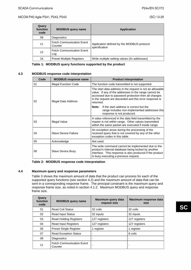
SCADA Communications
P24x/EN SC/I72 MiCOM P40 Agile P241, P242, P243 (SC) 13-25
SC
Query function
code MODBUS query name Application
08 Diagnostics
Application defined by the MODBUS protocol specification
11 Fetch Communication Event Counter
12 Fetch Communication Event Log
16 Preset Multiple Registers Write multiple setting values (4x addresses)
Table 1: MODBUS query functions supported by the product
4.3 MODBUS response code interpretation Code MODBUS response name Product interpretation
01 Illegal Function Code The function code transmitted is not supported.
02 Illegal Data Address
The start data address in the request is not an allowable value. If any of the addresses in the range cannot be accessed due to password protection then all changes in the request are discarded and this error response is returned. Note: If the start address is correct but the range includes non-implemented addresses this response is not produced.
03 Illegal Value A value referenced in the data field transmitted by the master is not within range. Other values transmitted within the same packet are executed if inside range.
04 Slave Device Failure An exception arose during the processing of the received query that is not covered by any of the other exception codes in this table.
05 Acknowledge Not used.
06 Slave Device Busy
The write command cannot be implemented due to the product’s internal database being locked by another interface. This response is also produced if the product is busy executing a previous request.
Table 2: MODBUS response code interpretation
4.4 Maximum query and response parameters Table 3 shows the maximum amount of data that the product can process for each of the supported query functions (see section 4.2) and the maximum amount of data that can be sent in a corresponding response frame. The principal constraint is the maximum query and response frame size, as noted in section 4.1.2. Maximum MODBUS query and response frame size.
Query function
code MODBUS query name Maximum query data
request size Maximum response data
size
01 Read Coil Status 32 coils 32 coils
02 Read Input Status 32 inputs 32 inputs
03 Read Holding Registers 127 registers 127 registers
04 Read Input Registers 127 registers 127 registers
06 Preset Single Register 1 register 1 register
07 Read Exception Status - 8 coils
08 Diagnostics - -
11 Fetch Communication Event Counter - -
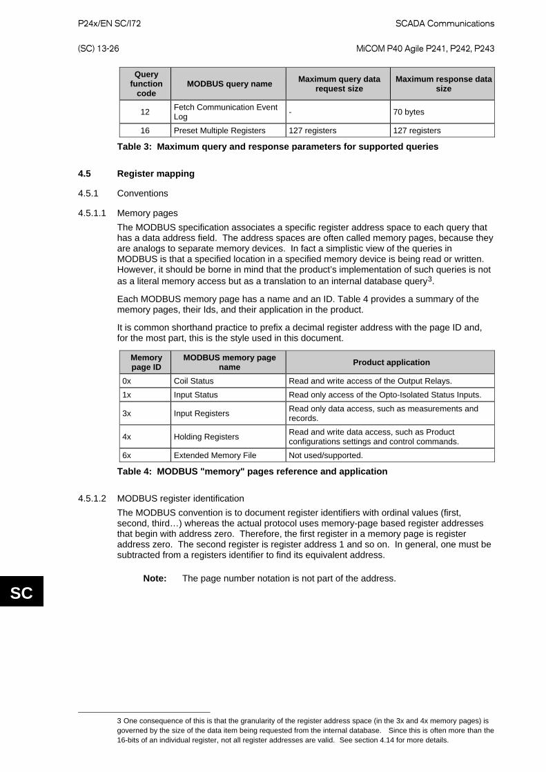
P24x/EN SC/I72
SCADA Communications (SC) 13-26 MiCOM P40 Agile P241, P242, P243
SC
Query function
code MODBUS query name Maximum query data
request size Maximum response data
size
12 Fetch Communication Event Log - 70 bytes
16 Preset Multiple Registers 127 registers 127 registers
Table 3: Maximum query and response parameters for supported queries
4.5 Register mapping
4.5.1 Conventions
4.5.1.1 Memory pages The MODBUS specification associates a specific register address space to each query that has a data address field. The address spaces are often called memory pages, because they are analogs to separate memory devices. In fact a simplistic view of the queries in MODBUS is that a specified location in a specified memory device is being read or written. However, it should be borne in mind that the product’s implementation of such queries is not as a literal memory access but as a translation to an internal database query3.
Each MODBUS memory page has a name and an ID. Table 4 provides a summary of the memory pages, their Ids, and their application in the product.
It is common shorthand practice to prefix a decimal register address with the page ID and, for the most part, this is the style used in this document.
Memory page ID
MODBUS memory page name Product application
0x Coil Status Read and write access of the Output Relays.
1x Input Status Read only access of the Opto-Isolated Status Inputs.
3x Input Registers Read only data access, such as measurements and records.
4x Holding Registers Read and write data access, such as Product configurations settings and control commands.
6x Extended Memory File Not used/supported.
Table 4: MODBUS "memory" pages reference and application
4.5.1.2 MODBUS register identification The MODBUS convention is to document register identifiers with ordinal values (first, second, third…) whereas the actual protocol uses memory-page based register addresses that begin with address zero. Therefore, the first register in a memory page is register address zero. The second register is register address 1 and so on. In general, one must be subtracted from a registers identifier to find its equivalent address.
Note: The page number notation is not part of the address.
3 One consequence of this is that the granularity of the register address space (in the 3x and 4x memory pages) is governed by the size of the data item being requested from the internal database. Since this is often more than the 16-bits of an individual register, not all register addresses are valid. See section 4.14 for more details.
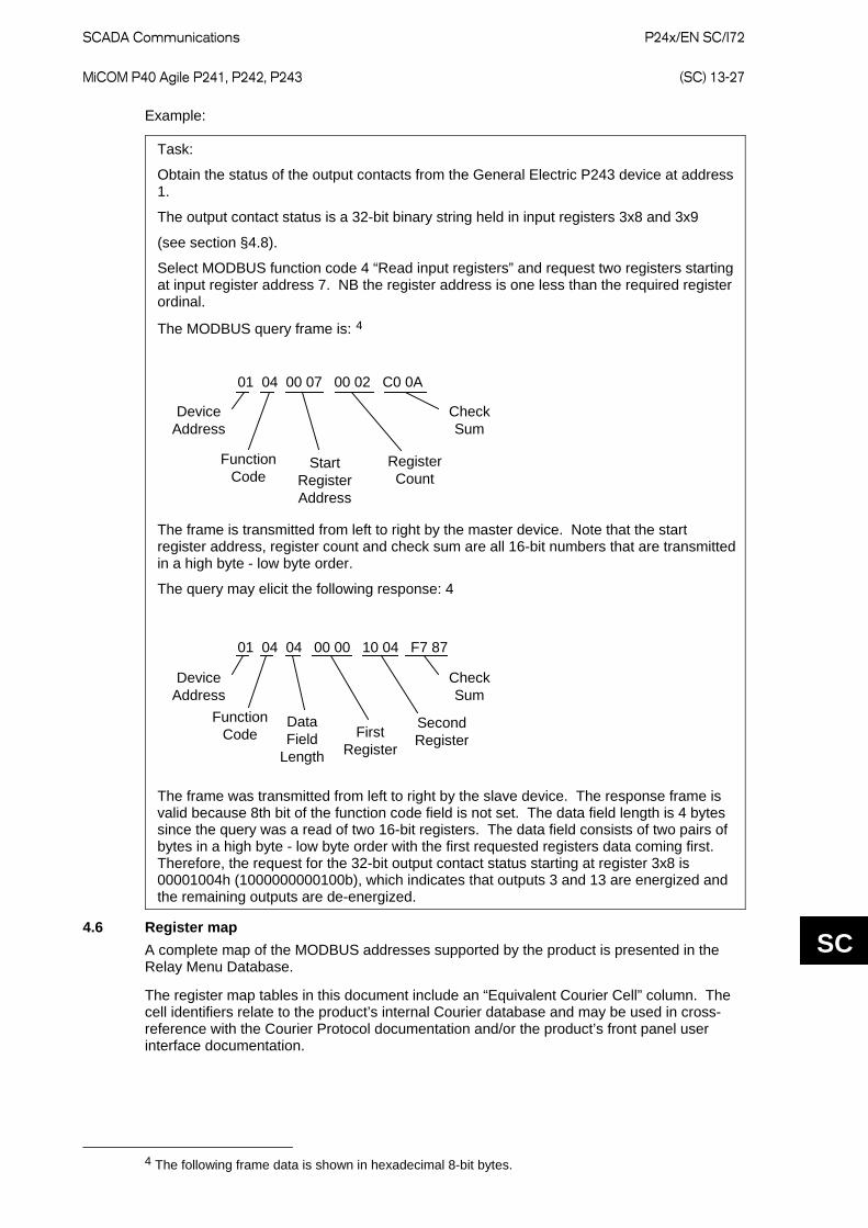
SCADA Communications
P24x/EN SC/I72 MiCOM P40 Agile P241, P242, P243 (SC) 13-27
SC
Example:
Task:
Obtain the status of the output contacts from the General Electric P243 device at address 1.
The output contact status is a 32-bit binary string held in input registers 3x8 and 3x9
(see section §4.8).
Select MODBUS function code 4 “Read input registers” and request two registers starting at input register address 7. NB the register address is one less than the required register ordinal.
The MODBUS query frame is: 4
01 04 00 07 00 02 C0 0A
DeviceAddress
FunctionCode
StartRegisterAddress
RegisterCount
CheckSum
The frame is transmitted from left to right by the master device. Note that the start register address, register count and check sum are all 16-bit numbers that are transmitted in a high byte - low byte order.
The query may elicit the following response: 4
01 04 04 00 00 10 04 F7 87
DeviceAddress
FunctionCode First
Register
SecondRegister
CheckSum
DataField
Length
The frame was transmitted from left to right by the slave device. The response frame is valid because 8th bit of the function code field is not set. The data field length is 4 bytes since the query was a read of two 16-bit registers. The data field consists of two pairs of bytes in a high byte - low byte order with the first requested registers data coming first. Therefore, the request for the 32-bit output contact status starting at register 3x8 is 00001004h (1000000000100b), which indicates that outputs 3 and 13 are energized and the remaining outputs are de-energized.
4.6 Register map A complete map of the MODBUS addresses supported by the product is presented in the Relay Menu Database.
The register map tables in this document include an “Equivalent Courier Cell” column. The cell identifiers relate to the product’s internal Courier database and may be used in cross-reference with the Courier Protocol documentation and/or the product’s front panel user interface documentation.
4 The following frame data is shown in hexadecimal 8-bit bytes.
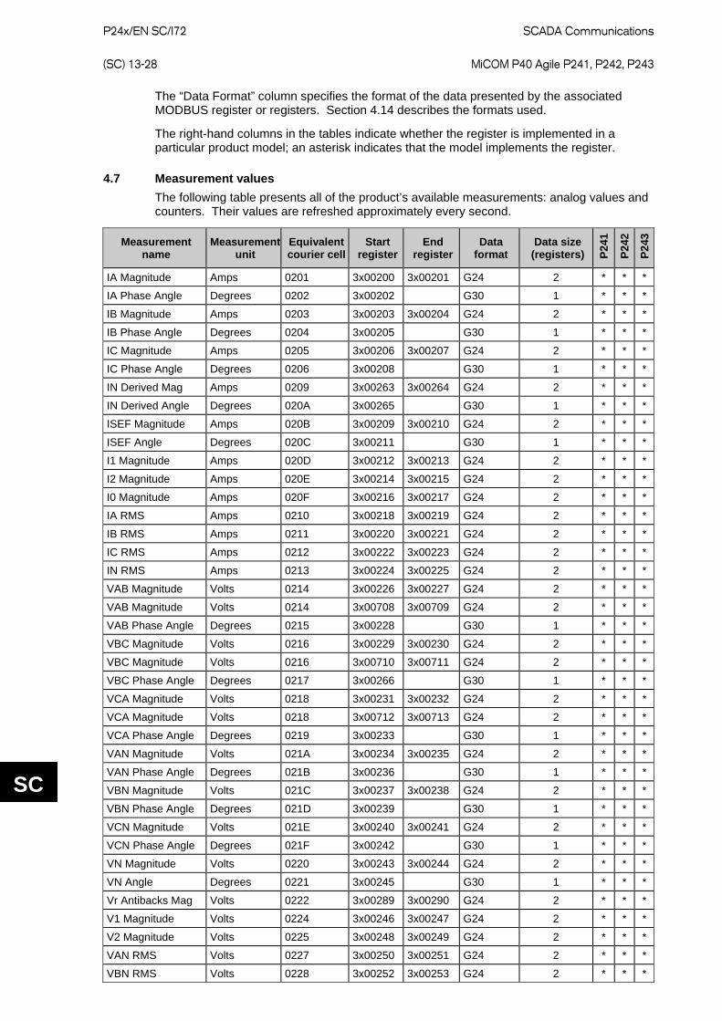
P24x/EN SC/I72
SCADA Communications (SC) 13-28 MiCOM P40 Agile P241, P242, P243
SC
The “Data Format” column specifies the format of the data presented by the associated MODBUS register or registers. Section 4.14 describes the formats used.
The right-hand columns in the tables indicate whether the register is implemented in a particular product model; an asterisk indicates that the model implements the register.
4.7 Measurement values The following table presents all of the product’s available measurements: analog values and counters. Their values are refreshed approximately every second.
Measurement name
Measurement unit
Equivalent courier cell
Start register
End register
Data format
Data size (registers) P2
41
P242
P243
IA Magnitude Amps 0201 3x00200 3x00201 G24 2 * * *
IA Phase Angle Degrees 0202 3x00202 G30 1 * * *
IB Magnitude Amps 0203 3x00203 3x00204 G24 2 * * *
IB Phase Angle Degrees 0204 3x00205 G30 1 * * *
IC Magnitude Amps 0205 3x00206 3x00207 G24 2 * * *
IC Phase Angle Degrees 0206 3x00208 G30 1 * * *
IN Derived Mag Amps 0209 3x00263 3x00264 G24 2 * * *
IN Derived Angle Degrees 020A 3x00265 G30 1 * * *
ISEF Magnitude Amps 020B 3x00209 3x00210 G24 2 * * *
ISEF Angle Degrees 020C 3x00211 G30 1 * * *
I1 Magnitude Amps 020D 3x00212 3x00213 G24 2 * * *
I2 Magnitude Amps 020E 3x00214 3x00215 G24 2 * * *
I0 Magnitude Amps 020F 3x00216 3x00217 G24 2 * * *
IA RMS Amps 0210 3x00218 3x00219 G24 2 * * *
IB RMS Amps 0211 3x00220 3x00221 G24 2 * * *
IC RMS Amps 0212 3x00222 3x00223 G24 2 * * *
IN RMS Amps 0213 3x00224 3x00225 G24 2 * * *
VAB Magnitude Volts 0214 3x00226 3x00227 G24 2 * * *
VAB Magnitude Volts 0214 3x00708 3x00709 G24 2 * * *
VAB Phase Angle Degrees 0215 3x00228 G30 1 * * *
VBC Magnitude Volts 0216 3x00229 3x00230 G24 2 * * *
VBC Magnitude Volts 0216 3x00710 3x00711 G24 2 * * *
VBC Phase Angle Degrees 0217 3x00266 G30 1 * * *
VCA Magnitude Volts 0218 3x00231 3x00232 G24 2 * * *
VCA Magnitude Volts 0218 3x00712 3x00713 G24 2 * * *
VCA Phase Angle Degrees 0219 3x00233 G30 1 * * *
VAN Magnitude Volts 021A 3x00234 3x00235 G24 2 * * *
VAN Phase Angle Degrees 021B 3x00236 G30 1 * * *
VBN Magnitude Volts 021C 3x00237 3x00238 G24 2 * * *
VBN Phase Angle Degrees 021D 3x00239 G30 1 * * *
VCN Magnitude Volts 021E 3x00240 3x00241 G24 2 * * *
VCN Phase Angle Degrees 021F 3x00242 G30 1 * * *
VN Magnitude Volts 0220 3x00243 3x00244 G24 2 * * *
VN Angle Degrees 0221 3x00245 G30 1 * * *
Vr Antibacks Mag Volts 0222 3x00289 3x00290 G24 2 * * *
V1 Magnitude Volts 0224 3x00246 3x00247 G24 2 * * *
V2 Magnitude Volts 0225 3x00248 3x00249 G24 2 * * *
VAN RMS Volts 0227 3x00250 3x00251 G24 2 * * *
VBN RMS Volts 0228 3x00252 3x00253 G24 2 * * *
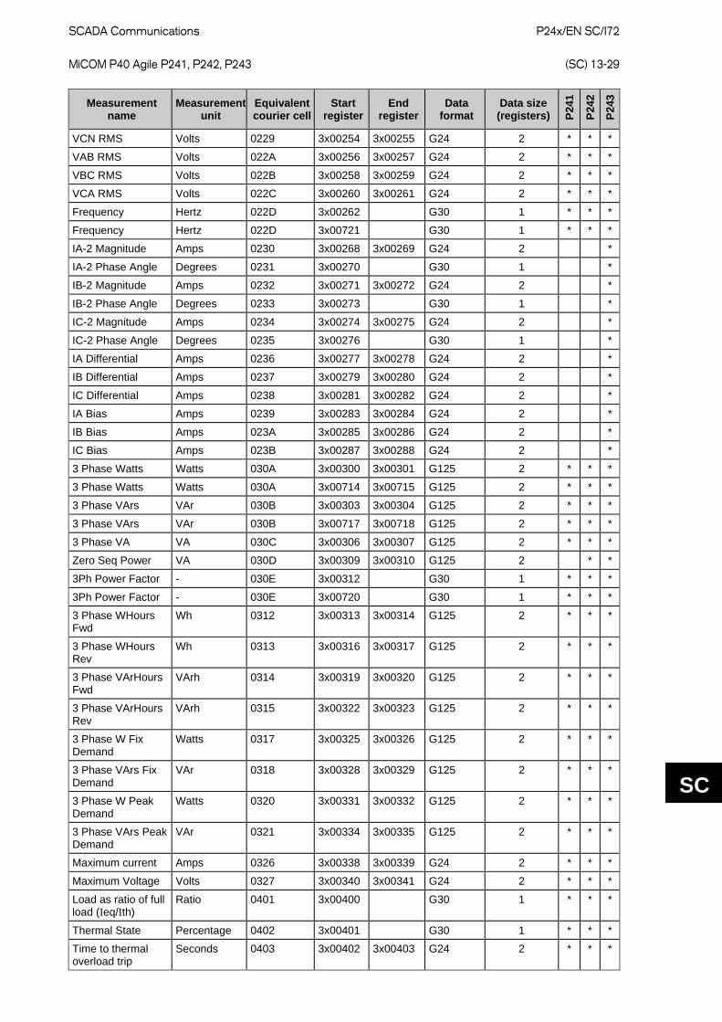
SCADA Communications
P24x/EN SC/I72 MiCOM P40 Agile P241, P242, P243 (SC) 13-29
SC
Measurement name
Measurement unit
Equivalent courier cell
Start register
End register
Data format
Data size (registers) P2
41
P242
P243
VCN RMS Volts 0229 3x00254 3x00255 G24 2 * * *
VAB RMS Volts 022A 3x00256 3x00257 G24 2 * * *
VBC RMS Volts 022B 3x00258 3x00259 G24 2 * * *
VCA RMS Volts 022C 3x00260 3x00261 G24 2 * * *
Frequency Hertz 022D 3x00262 G30 1 * * *
Frequency Hertz 022D 3x00721 G30 1 * * *
IA-2 Magnitude Amps 0230 3x00268 3x00269 G24 2 *
IA-2 Phase Angle Degrees 0231 3x00270 G30 1 *
IB-2 Magnitude Amps 0232 3x00271 3x00272 G24 2 *
IB-2 Phase Angle Degrees 0233 3x00273 G30 1 *
IC-2 Magnitude Amps 0234 3x00274 3x00275 G24 2 *
IC-2 Phase Angle Degrees 0235 3x00276 G30 1 *
IA Differential Amps 0236 3x00277 3x00278 G24 2 *
IB Differential Amps 0237 3x00279 3x00280 G24 2 *
IC Differential Amps 0238 3x00281 3x00282 G24 2 *
IA Bias Amps 0239 3x00283 3x00284 G24 2 *
IB Bias Amps 023A 3x00285 3x00286 G24 2 *
IC Bias Amps 023B 3x00287 3x00288 G24 2 *
3 Phase Watts Watts 030A 3x00300 3x00301 G125 2 * * *
3 Phase Watts Watts 030A 3x00714 3x00715 G125 2 * * *
3 Phase VArs VAr 030B 3x00303 3x00304 G125 2 * * *
3 Phase VArs VAr 030B 3x00717 3x00718 G125 2 * * *
3 Phase VA VA 030C 3x00306 3x00307 G125 2 * * *
Zero Seq Power VA 030D 3x00309 3x00310 G125 2 * *
3Ph Power Factor - 030E 3x00312 G30 1 * * *
3Ph Power Factor - 030E 3x00720 G30 1 * * *
3 Phase WHours Fwd
Wh 0312 3x00313 3x00314 G125 2 * * *
3 Phase WHours Rev
Wh 0313 3x00316 3x00317 G125 2 * * *
3 Phase VArHours Fwd
VArh 0314 3x00319 3x00320 G125 2 * * *
3 Phase VArHours Rev
VArh 0315 3x00322 3x00323 G125 2 * * *
3 Phase W Fix Demand
Watts 0317 3x00325 3x00326 G125 2 * * *
3 Phase VArs Fix Demand
VAr 0318 3x00328 3x00329 G125 2 * * *
3 Phase W Peak Demand
Watts 0320 3x00331 3x00332 G125 2 * * *
3 Phase VArs Peak Demand
VAr 0321 3x00334 3x00335 G125 2 * * *
Maximum current Amps 0326 3x00338 3x00339 G24 2 * * *
Maximum Voltage Volts 0327 3x00340 3x00341 G24 2 * * *
Load as ratio of full load (Ieq/Ith)
Ratio 0401 3x00400 G30 1 * * *
Thermal State Percentage 0402 3x00401 G30 1 * * *
Time to thermal overload trip
Seconds 0403 3x00402 3x00403 G24 2 * * *

P24x/EN SC/I72
SCADA Communications (SC) 13-30 MiCOM P40 Agile P241, P242, P243
SC
Measurement name
Measurement unit
Equivalent courier cell
Start register
End register
Data format
Data size (registers) P2
41
P242
P243
RTD 1 Temperature Celsius 0405 3x00404 G10 1 * * *
RTD 2 Temperature Celsius 0406 3x00405 G10 1 * * *
RTD 3 Temperature Celsius 0407 3x00406 G10 1 * * *
RTD 4 Temperature Celsius 0408 3x00407 G10 1 * * *
RTD 5 Temperature Celsius 0409 3x00408 G10 1 * * *
RTD 6 Temperature Celsius 041A 3x00409 G10 1 * * *
RTD 7 Temperature Celsius 041B 3x00410 G10 1 * * *
RTD 8 Temperature Celsius 041C 3x00411 G10 1 * * *
RTD 9 Temperature Celsius 041D 3x00412 G10 1 * * *
RTD 10 Temperature
Celsius 041E 3x00413 G10 1 * * *
Nb of hot starts allowed
- 040F 3x00414 G1 1 * * *
Nb of cold starts allowed
- 0410 3x00415 G1 1 * * *
Time to next start Seconds 0411 3x00416 3x00417 G24 2 * * *
Last start time Seconds 0411 3x00416 3x00417 G24 2 * * *
Last start current Amps 0414 3x00420 3x00421 G24 2 * * *
Number of motor starts
- 0415 3x00422 G1 1 * * *
Number of emergency restarts
- 0417 3x00423 G1 1 * * *
Number of reacceleration
- 0419 3x00425 G1 1 * * *
Motor running hours Hours 041B 3x00427 3x00428 G125 2 * * *
RTD Open Cct - 041D 3x00429 G108 1 * * *
RTD Short Cct - 041E 3x00430 G109 1 * * *
RTD Data error - 041F 3x00431 G110 1 * * *
Num RTD hottest measurement
- 0421 3x00432 G1 1 * * *
Hottest RTD measurement
Celsius 0422 3x00433 G10 1 * * *
Analog Input 1 measurement
- 0424 3x00434 3x00435 G125 2 * * *
Analog Input 2 measurement
- 0425 3x00436 3x00437 G125 2 * * *
Analog Input 3 measurement
- 0426 3x00438 3x00439 G125 2 * * *
Analog Input 4 measurement
- 0427 3x00440 3x00441 G125 2 * * *
Nb of control trips - 0501 3x00500 G1 1 * * *
Nb of Trip Ith> - 0502 3x00501 G1 1 * * *
Nb of Trip Icc>1 - 0503 3x00502 G1 1 * * *
Nb of Trip Icc>2 - 0504 3x00531 G1 1 * * *
Nb of Trip ISEF>1 - 0505 3x00503 G1 1 * * *
Nb of Trip ISEF>2 - 0506 3x00504 G1 1 * * *
Nb of Trip IEFD>1 - 0507 3x00532 G1 1 * * *
Nb of Trip IEFD>2 - 0508 3x00533 G1 1 * * *
Nb of Trip I2>1 - 0509 3x00505 G1 1 * * *
Nb of Trip I2>2 - 050A 3x00506 G1 1 * * *
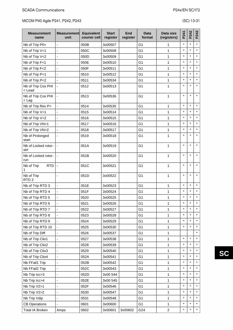
SCADA Communications
P24x/EN SC/I72 MiCOM P40 Agile P241, P242, P243 (SC) 13-31
SC
Measurement name
Measurement unit
Equivalent courier cell
Start register
End register
Data format
Data size (registers) P2
41
P242
P243
Nb of Trip P0> - 050B 3x00507 G1 1 * * *
Nb of Trip V<1 - 050C 3x00508 G1 1 * * *
Nb of Trip V<2 - 050D 3x00509 G1 1 * * *
Nb of Trip F<1 - 050E 3x00510 G1 1 * * *
Nb of Trip F<2 - 050F 3x00511 G1 1 * * *
Nb of Trip P<1 - 0510 3x00512 G1 1 * * *
Nb of Trip P<2 - 0511 3x00534 G1 1 * * *
Nb of Trip Cos PHI < Lead
- 0512 3x00513 G1 1 * * *
Nb of Trip Cos PHI < Lag
- 0513 3x00536 G1 1 * * *
Nb of Trip Rev P> - 0514 3x00535 G1 1 * * *
Nb of Trip V>1 - 0515 3x00514 G1 1 * * *
Nb of Trip V>2 - 0516 3x00515 G1 1 * * *
Nb of Trip VN>1 - 0517 3x00516 G1 1 * * *
Nb of Trip VN>2 - 0518 3x00517 G1 1 * * *
Nb of Prolonged start
- 0519 3x00518 G1 1 * * *
Nb of Locked rotor-strt
- 051A 3x00519 G1 1 * * *
Nb of Locked rotor-run
- 051B 3x00520 G1 1 * * *
Nb of Trip RTD 1
- 051C 3x00521 G1 1 * * *
Nb of Trip RTD 2
- 051D 3x00522 G1 1 * * *
Nb of Trip RTD 3 - 051E 3x00523 G1 1 * * *
Nb of Trip RTD 4 - 051F 3x00524 G1 1 * * *
Nb of Trip RTD 5 - 0520 3x00525 G1 1 * * *
Nb of Trip RTD 6 - 0521 3x00526 G1 1 * * *
Nb of Trip RTD 7 - 0522 3x00527 G1 1 * * *
Nb of Trip RTD 8 - 0523 3x00528 G1 1 * * *
Nb of Trip RTD 9 - 0524 3x00529 G1 1 * * *
Nb of Trip RTD 10 - 0525 3x00530 G1 1 * * *
Nb of Trip Diff - 0526 3x00537 G1 1 *
Nb of Trip Clio1 - 0527 3x00538 G1 1 * * *
Nb of Trip Clio2 - 0528 3x00539 G1 1 * * *
Nb of Trip Clio3 - 0529 3x00540 G1 1 * * *
Nb of Trip Clio4 - 052A 3x00541 G1 1 * * *
Nb FFail1 Trip - 052B 3x00542 G1 1 * * *
Nb FFail2 Trip - 052C 3x00543 G1 1 * * *
Nb Trip Icc>3 - 052D 3x00 544 G1 1 * * *
Nb Trip Icc>4 - 052E 3x00 545 G1 1 * * *
Nb Trip V2>1 - 052F 3x00546 G1 1 * * *
Nb Trip V2>2 - 0530 3x00547 G1 1 * * *
Nb Trip Vdip - 0531 3x00548 G1 1 * * *
CB Operations - 0601 3x00600 G1 1 * * *
Total IA Broken Amps 0602 3x00601 3x00602 G24 2 * * *
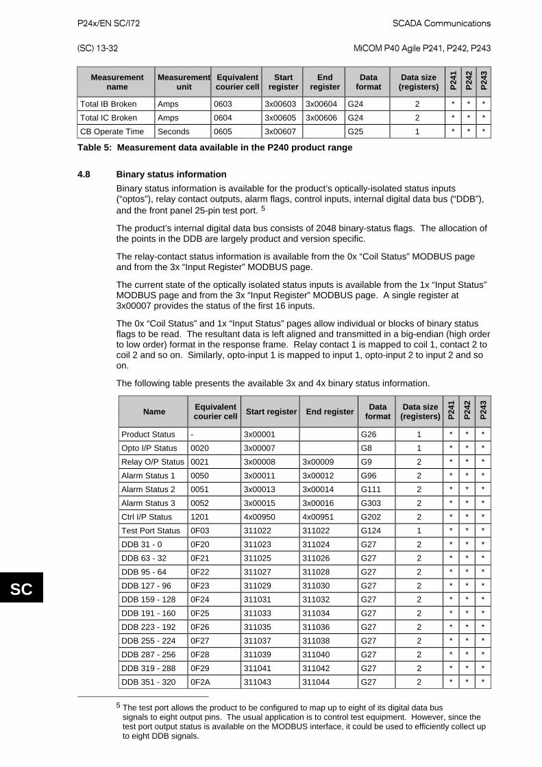
P24x/EN SC/I72
SCADA Communications (SC) 13-32 MiCOM P40 Agile P241, P242, P243
SC
Measurement name
Measurement unit
Equivalent courier cell
Start register
End register
Data format
Data size (registers) P2
41
P242
P243
Total IB Broken Amps 0603 3x00603 3x00604 G24 2 * * *
Total IC Broken Amps 0604 3x00605 3x00606 G24 2 * * *
CB Operate Time Seconds 0605 3x00607 G25 1 * * *
Table 5: Measurement data available in the P240 product range
4.8 Binary status information Binary status information is available for the product’s optically-isolated status inputs (“optos”), relay contact outputs, alarm flags, control inputs, internal digital data bus (“DDB”), and the front panel 25-pin test port. 5
The product’s internal digital data bus consists of 2048 binary-status flags. The allocation of the points in the DDB are largely product and version specific.
The relay-contact status information is available from the 0x “Coil Status” MODBUS page and from the 3x “Input Register” MODBUS page.
The current state of the optically isolated status inputs is available from the 1x “Input Status” MODBUS page and from the 3x “Input Register” MODBUS page. A single register at 3x00007 provides the status of the first 16 inputs.
The 0x “Coil Status” and 1x “Input Status” pages allow individual or blocks of binary status flags to be read. The resultant data is left aligned and transmitted in a big-endian (high order to low order) format in the response frame. Relay contact 1 is mapped to coil 1, contact 2 to coil 2 and so on. Similarly, opto-input 1 is mapped to input 1, opto-input 2 to input 2 and so on.
The following table presents the available 3x and 4x binary status information.
Name Equivalent courier cell Start register End register Data
format Data size
(registers) P241
P242
P243
Product Status - 3x00001 G26 1 * * *
Opto I/P Status 0020 3x00007 G8 1 * * *
Relay O/P Status 0021 3x00008 3x00009 G9 2 * * *
Alarm Status 1 0050 3x00011 3x00012 G96 2 * * *
Alarm Status 2 0051 3x00013 3x00014 G111 2 * * *
Alarm Status 3 0052 3x00015 3x00016 G303 2 * * *
Ctrl I/P Status 1201 4x00950 4x00951 G202 2 * * *
Test Port Status 0F03 311022 311022 G124 1 * * *
DDB 31 - 0 0F20 311023 311024 G27 2 * * *
DDB 63 - 32 0F21 311025 311026 G27 2 * * *
DDB 95 - 64 0F22 311027 311028 G27 2 * * *
DDB 127 - 96 0F23 311029 311030 G27 2 * * *
DDB 159 - 128 0F24 311031 311032 G27 2 * * *
DDB 191 - 160 0F25 311033 311034 G27 2 * * *
DDB 223 - 192 0F26 311035 311036 G27 2 * * *
DDB 255 - 224 0F27 311037 311038 G27 2 * * *
DDB 287 - 256 0F28 311039 311040 G27 2 * * *
DDB 319 - 288 0F29 311041 311042 G27 2 * * *
DDB 351 - 320 0F2A 311043 311044 G27 2 * * *
5 The test port allows the product to be configured to map up to eight of its digital data bus
signals to eight output pins. The usual application is to control test equipment. However, since the test port output status is available on the MODBUS interface, it could be used to efficiently collect up to eight DDB signals.
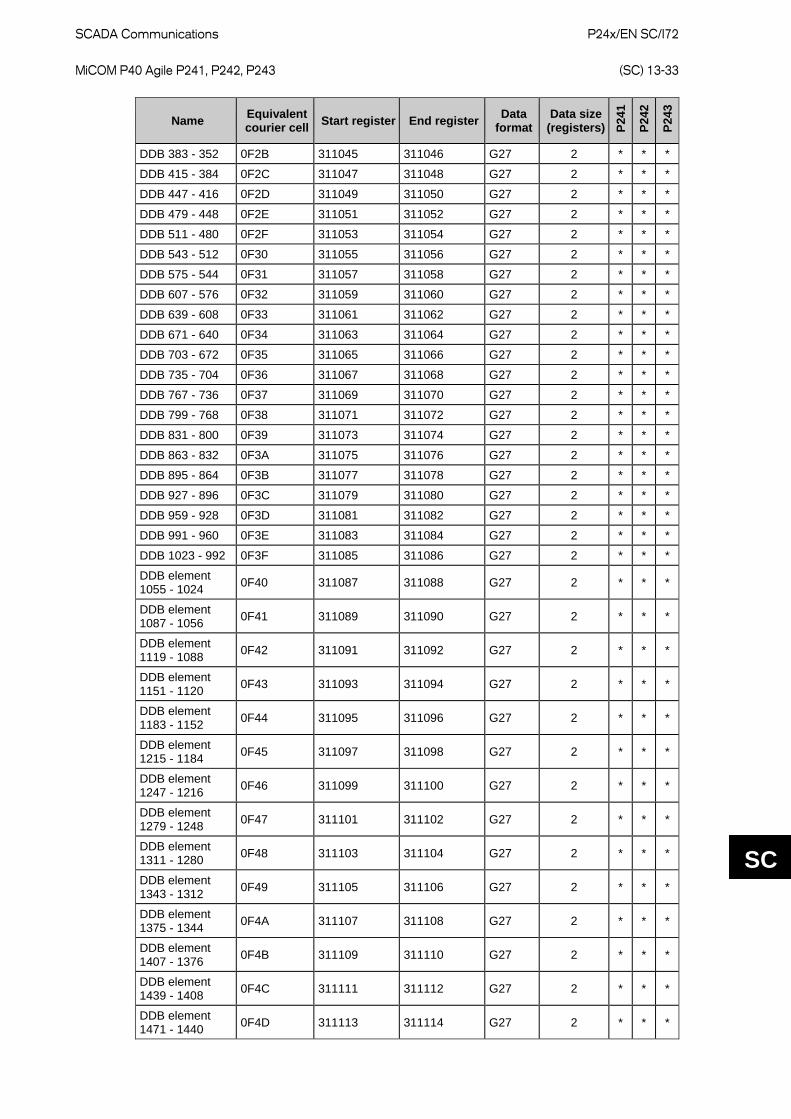
SCADA Communications
P24x/EN SC/I72 MiCOM P40 Agile P241, P242, P243 (SC) 13-33
SC
Name Equivalent courier cell Start register End register Data
format Data size
(registers) P241
P242
P243
DDB 383 - 352 0F2B 311045 311046 G27 2 * * *
DDB 415 - 384 0F2C 311047 311048 G27 2 * * *
DDB 447 - 416 0F2D 311049 311050 G27 2 * * *
DDB 479 - 448 0F2E 311051 311052 G27 2 * * *
DDB 511 - 480 0F2F 311053 311054 G27 2 * * *
DDB 543 - 512 0F30 311055 311056 G27 2 * * *
DDB 575 - 544 0F31 311057 311058 G27 2 * * *
DDB 607 - 576 0F32 311059 311060 G27 2 * * *
DDB 639 - 608 0F33 311061 311062 G27 2 * * *
DDB 671 - 640 0F34 311063 311064 G27 2 * * *
DDB 703 - 672 0F35 311065 311066 G27 2 * * *
DDB 735 - 704 0F36 311067 311068 G27 2 * * *
DDB 767 - 736 0F37 311069 311070 G27 2 * * *
DDB 799 - 768 0F38 311071 311072 G27 2 * * *
DDB 831 - 800 0F39 311073 311074 G27 2 * * *
DDB 863 - 832 0F3A 311075 311076 G27 2 * * *
DDB 895 - 864 0F3B 311077 311078 G27 2 * * *
DDB 927 - 896 0F3C 311079 311080 G27 2 * * *
DDB 959 - 928 0F3D 311081 311082 G27 2 * * *
DDB 991 - 960 0F3E 311083 311084 G27 2 * * *
DDB 1023 - 992 0F3F 311085 311086 G27 2 * * *
DDB element 1055 - 1024 0F40 311087 311088 G27 2 * * *
DDB element 1087 - 1056 0F41 311089 311090 G27 2 * * *
DDB element 1119 - 1088 0F42 311091 311092 G27 2 * * *
DDB element 1151 - 1120 0F43 311093 311094 G27 2 * * *
DDB element 1183 - 1152 0F44 311095 311096 G27 2 * * *
DDB element 1215 - 1184 0F45 311097 311098 G27 2 * * *
DDB element 1247 - 1216 0F46 311099 311100 G27 2 * * *
DDB element 1279 - 1248 0F47 311101 311102 G27 2 * * *
DDB element 1311 - 1280 0F48 311103 311104 G27 2 * * *
DDB element 1343 - 1312 0F49 311105 311106 G27 2 * * *
DDB element 1375 - 1344 0F4A 311107 311108 G27 2 * * *
DDB element 1407 - 1376 0F4B 311109 311110 G27 2 * * *
DDB element 1439 - 1408 0F4C 311111 311112 G27 2 * * *
DDB element 1471 - 1440 0F4D 311113 311114 G27 2 * * *
P24x/EN SC/I72
SCADA Communications (SC) 13-34 MiCOM P40 Agile P241, P242, P243
SC
Name Equivalent courier cell Start register End register Data
format Data size
(registers) P241
P242
P243
DDB element 1503 - 1472 0F4E 311115 311116 G27 2 * * *
DDB element 1535 - 1504 0F4F 311117 311118 G27 2 * * *
DDB element 1567 - 1536 0F50 311119 311120 G27 2 * * *
DDB element 1599 - 1568 0F51 311121 311122 G27 2 * * *
DDB element 1631 - 1600 0F52 311123 311124 G27 2 * * *
DDB element 1663 - 1632 0F53 311125 311126 G27 2 * * *
DDB element 1695 - 1664 0F54 311127 311128 G27 2 * * *
DDB element 1727 - 1696 0F55 311129 311130 G27 2 * * *
DDB element 1759 - 1728 0F56 311131 311132 G27 2 * * *
DDB element 1791 - 1760 0F57 311133 311134 G27 2 * * *
DDB element 1823 - 1792 0F58 311135 311136 G27 2 * * *
DDB element 1855 - 1824 0F59 311137 311138 G27 2 * * *
DDB element 1887 - 1856 0F5A 311139 311140 G27 2 * * *
DDB element 1919 - 1888 0F5B 311141 311142 G27 2 * * *
DDB element 1951 - 1920 0F5C 311143 311144 G27 2 * * *
DDB element 1983 - 1952 0F5D 311145 311146 G27 2 * * *
DDB element 2015 - 1984 0F5E 311147 311148 G27 2 * * *
DDB element 2047 - 2016 0F5F 311149 311150 G27 2 * * *
Table 6: Binary status information available in the P240 product range
4.9 Measurement and binary status 3x register sets The data available from the 3x input registers is arranged into register sets. A register set is a fixed collection of values in a contiguous block of register addresses. The advantage of this is that multiple values may be read with a single MODBUS query, function code 4 “Read Input Registers”, up to the maximum data limits of the query (see section 4.4).
The definition of a register-set is specified by the selection of a start and end address, which can span multiple contiguous values in the 3x Register. The only rule being that a register set must not result in an attempt to read only part of a multi-register data type (see section 4.14). It is permissible for a register set to span unused register locations, in which case a value of zero is returned for each such register location.
Some examples of useful register sets are:
• 3x200 to 3x288 provides a selection of measurements. • 311023 to 311150 provide the DDB status • 3x404 to 3x413 provide the ten RTD measurement values
SCADA Communications
P24x/EN SC/I72 MiCOM P40 Agile P241, P242, P243 (SC) 13-35
SC
There are many other possibilities dependent on your application and an appraisal of the 3x Register Map. The capabilities of the MODBUS master device, performance targets, and communications latencies may also influence the degree to which multiple values are read as register sets, as opposed to individually.
4.10 Controls The following table presents MODBUS 4x “Holding Registers” that allow the external system to control aspects of the product’s behavior, configuration, records, or items of plant connected to the product such as circuit breakers.
The column Command or setting indicates whether the control is a self-resetting “Command” or a state based “Setting”.
“Command” controls automatically return to their default value when the control action has been completed. For example, writing the “trip” value to the “CB Trip/Close” control will result in the controlled circuit breaker opening (if CB remote control is enabled, the CB has a valid state, and it was closed). The value of the “CB Trip/Close” register will automatically return to “no operation”. This may lead to problems with masters that attempt to verify write requests by reading back the written value.
“Setting” controls maintain the written value, assuming that it was accepted. For example the “Active Setting Group” register reports the current active group on reads and accepts writes with a valid setting group number to change the active group to the one specified. (This assumes that setting group selection by optically isolated status inputs has not been enabled and that the specified group is enabled).
Entries without a defined setting range, as per the “min.”, “max.” and “step” columns, are binary-string values whose pattern is defined by its stated data type.
4.11 Event extraction The product is capable of storing 512 event records in battery backed memory. An event record consists of a time stamp, a record type, and a set of information fields. The record type and the information fields record the event that occurred at the time captured by the time stamp.
The product has several classes of event record:
• Alarm events • Opto-isolated status input events • Relay contact output events • Protection/DDB operation events • Fault data capture events • General events
Note: The product provides an “event filtering” feature that may be used to prevent specific events from being logged. The event filter is configured in the “Record Control” section of the product’s menu database in the MiCOM S1 Studio configuration tool.
The product supports two methods of event extraction providing either automatic or manual extraction of the stored event, fault, and maintenance records.
It is important to appreciate that the product stores event, fault, and maintenance records in three separate queues. As entries are added to the fault and maintenance queues a corresponding event is added to the event queue. Each queue is of different length and each queue may be individually cleared (see section 4.11.4). It is therefore possible to have a fault event or a maintenance event entry in the event queue with no corresponding entry in the associated queue because it has been overwritten or deleted.
The manual extraction procedure (section 4.11.1) allows each of these three queues to be read independently.
P24x/EN SC/I72
SCADA Communications (SC) 13-36 MiCOM P40 Agile P241, P242, P243
SC
The automatic extraction procedure (section 4.11.2) reads records from the event queue. If the event record is either a fault or a maintenance record then the records extended data is read too, if it is available from their queues.
Note: Version 31 of the product introduced a new set of 3x registers for the presentation of the event and fault record data. These registers are used throughout the text of the following sub-sections. For legacy compatibility, the original registers are still provided. These are described as previous MODBUS address in the Relay Menu Database. They should not be used for new installations. See section 4.11.5 for additional information.
4.11.1 Manual extraction procedure There are three registers available to manually select stored records, there are also three read only registers allowing the number of stored records to be determined.
4x00100 - Select Event, 0 to 249
4x00101 - Select Fault, 0 to 4
4x00102 - Select Maintenance Record, 0 to 4
For each of the above registers, a value of zero represents the most recent stored record. The following registers can be read to indicate the numbers of the various types of record stored.
3x10000 - Number of stored event records
3x10001 - Number of stored fault records
3x10002 - Number of stored maintenance records
Each fault or maintenance record logged causes an event record to be created by the product. If this event record is selected the additional registers showing the fault or maintenance record details are also populated.
4.11.2 Automatic extraction procedure Automatic event-record extraction allows records to be extracted as they occur. Event records are extracted in sequential order, including any fault or maintenance data that may be associated with an event.
The MODBUS master can determine whether the product has any events stored that have not yet been extracted. This is performed by reading the product’s status register 3x00001 (G26 data type). If the event bit, of this register, is set then the product contains event records that have not yet been extracted.
To select the next event for sequential extraction, the master station writes a value of one to the record selection register 4x00400 (G18 data type). The event data together with any fault/maintenance data can be read from the registers specified in 4.11.3. Once the data has been read, the event record can be marked as having been read by writing a value of two to register 4x00400. Alternatively, since the G18 data type consists of bit fields, it is possible to both mark the current record as having been read and to automatically select the next unread record by writing a value of three to the register.
When the last (most recent) record has been accepted the event flag in the status register (3x00001) is reset. If the last record was accepted, by writing a value of three to the record selection register (4x00400), then a dummy record appears in the event-record registers, with an “Event Type” value of 255. Attempting to select another record, when none are available, results in a MODBUS exception code 3 - “Invalid value” (see section 4.3).
One possible event record extraction procedure is shown in Figure 6.
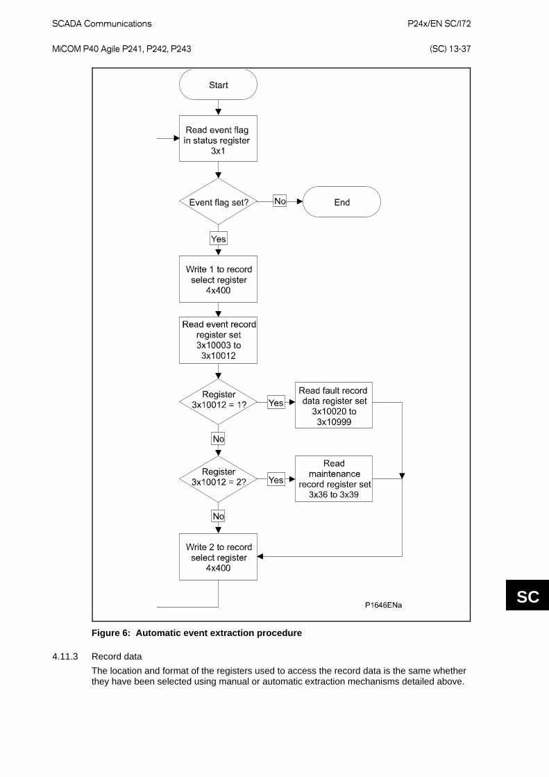
SCADA Communications
P24x/EN SC/I72 MiCOM P40 Agile P241, P242, P243 (SC) 13-37
SC
Figure 6: Automatic event extraction procedure
4.11.3 Record data The location and format of the registers used to access the record data is the same whether they have been selected using manual or automatic extraction mechanisms detailed above.
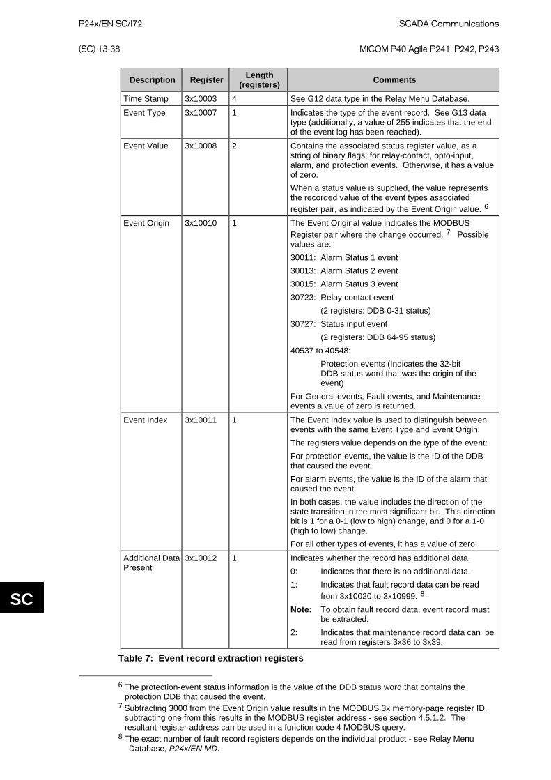
P24x/EN SC/I72
SCADA Communications (SC) 13-38 MiCOM P40 Agile P241, P242, P243
SC
Description Register Length (registers) Comments
Time Stamp 3x10003 4 See G12 data type in the Relay Menu Database.
Event Type 3x10007 1 Indicates the type of the event record. See G13 data type (additionally, a value of 255 indicates that the end of the event log has been reached).
Event Value 3x10008 2 Contains the associated status register value, as a string of binary flags, for relay-contact, opto-input, alarm, and protection events. Otherwise, it has a value of zero. When a status value is supplied, the value represents the recorded value of the event types associated register pair, as indicated by the Event Origin value. 6
Event Origin 3x10010 1 The Event Original value indicates the MODBUS Register pair where the change occurred. 7 Possible values are: 30011: Alarm Status 1 event 30013: Alarm Status 2 event 30015: Alarm Status 3 event 30723: Relay contact event (2 registers: DDB 0-31 status) 30727: Status input event (2 registers: DDB 64-95 status) 40537 to 40548: Protection events (Indicates the 32-bit DDB status word that was the origin of the event) For General events, Fault events, and Maintenance events a value of zero is returned.
Event Index 3x10011 1 The Event Index value is used to distinguish between events with the same Event Type and Event Origin. The registers value depends on the type of the event: For protection events, the value is the ID of the DDB that caused the event. For alarm events, the value is the ID of the alarm that caused the event. In both cases, the value includes the direction of the state transition in the most significant bit. This direction bit is 1 for a 0-1 (low to high) change, and 0 for a 1-0 (high to low) change. For all other types of events, it has a value of zero.
Additional Data Present
3x10012 1 Indicates whether the record has additional data. 0: Indicates that there is no additional data. 1: Indicates that fault record data can be read from 3x10020 to 3x10999. 8 Note: To obtain fault record data, event record must be extracted. 2: Indicates that maintenance record data can be read from registers 3x36 to 3x39.
Table 7: Event record extraction registers
6 The protection-event status information is the value of the DDB status word that contains the protection DDB that caused the event. 7 Subtracting 3000 from the Event Origin value results in the MODBUS 3x memory-page register ID, subtracting one from this results in the MODBUS register address - see section 4.5.1.2. The resultant register address can be used in a function code 4 MODBUS query. 8 The exact number of fault record registers depends on the individual product - see Relay Menu Database, P24x/EN MD.
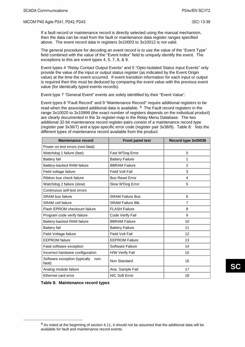
SCADA Communications
P24x/EN SC/I72 MiCOM P40 Agile P241, P242, P243 (SC) 13-39
SC
If a fault record or maintenance record is directly selected using the manual mechanism, then the data can be read from the fault or maintenance data register ranges specified above. The event record data in registers 3x10003 to 3x10012 is not valid.
The general procedure for decoding an event record is to use the value of the “Event Type” field combined with the value of the “Event Index” field to uniquely identify the event. The exceptions to this are event types 4, 5, 7, 8, & 9.
Event types 4 “Relay Contact Output Events“ and 5 “Opto-Isolated Status Input Events” only provide the value of the input or output status register (as indicated by the Event Origin value) at the time the event occurred. If event transition information for each input or output is required then this must be deduced by comparing the event value with the previous event value (for identically typed events records).
Event type 7 “General Event” events are solely identified by their “Event Value”.
Event types 8 “Fault Record” and 9 “Maintenance Record” require additional registers to be read when the associated additional data is available. 9 The Fault record registers in the range 3x10020 to 3x10999 (the exact number of registers depends on the individual product) are clearly documented in the 3x register-map in the Relay Menu Database. The two additional 32-bit maintenance record register-pairs consist of a maintenance record type (register pair 3x36/7) and a type-specific error code (register pair 3x38/9). Table 8: lists the different types of maintenance record available from the product.
Maintenance record Front panel text Record type 3x00036 Power on test errors (non-fatal)
Watchdog 1 failure (fast) Fast W'Dog Error 0
Battery fail Battery Failure 1
Battery-backed RAM failure BBRAM Failure 2
Field voltage failure Field Volt Fail 3
Ribbon bus check failure Bus Reset Error 4
Watchdog 2 failure (slow) Slow W'Dog Error 5
Continuous self-test errors
SRAM bus failure SRAM Failure Bus 6
SRAM cell failure SRAM Failure Blk. 7
Flash EPROM checksum failure FLASH Failure 8
Program code verify failure Code Verify Fail 9
Battery-backed RAM failure BBRAM Failure 10
Battery fail Battery Failure 11
Field Voltage failure Field Volt Fail 12
EEPROM failure EEPROM Failure 13
Fatal software exception Software Failure 14
Incorrect hardware configuration H/W Verify Fail 15
Software exception (typically non-fatal) Non Standard 16
Analog module failure Ana. Sample Fail 17
Ethernet card error NIC Soft Error 18
Table 8: Maintenance record types
9 As noted at the beginning of section 4.11, it should not be assumed that the additional data will be available for fault and maintenance record events.
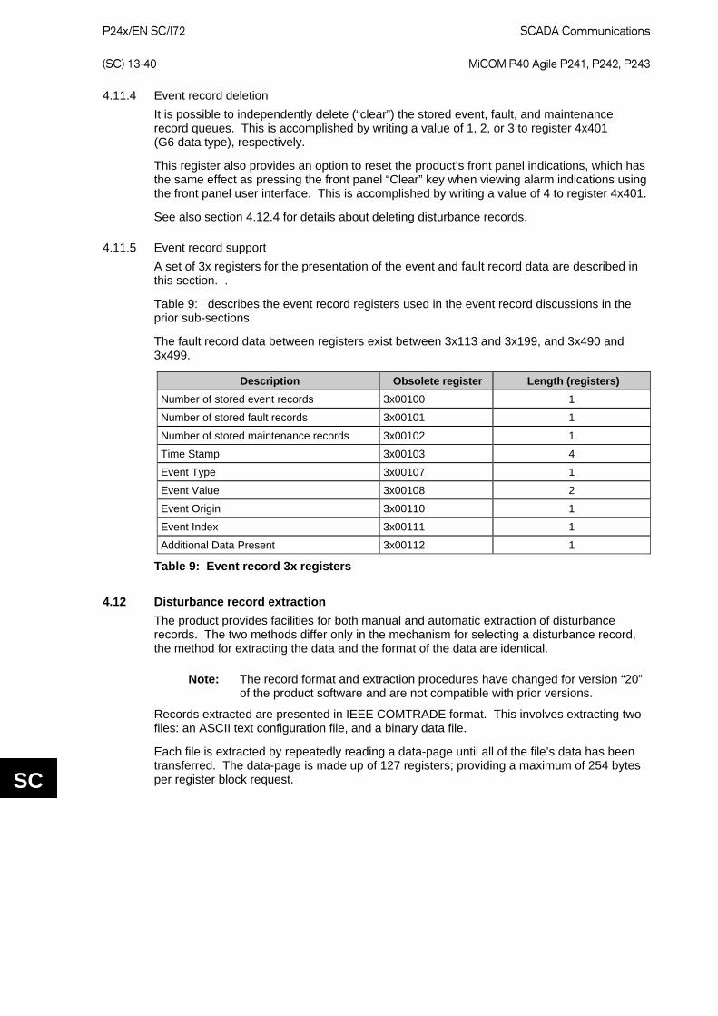
P24x/EN SC/I72
SCADA Communications (SC) 13-40 MiCOM P40 Agile P241, P242, P243
SC
4.11.4 Event record deletion It is possible to independently delete (“clear”) the stored event, fault, and maintenance record queues. This is accomplished by writing a value of 1, 2, or 3 to register 4x401 (G6 data type), respectively.
This register also provides an option to reset the product’s front panel indications, which has the same effect as pressing the front panel “Clear” key when viewing alarm indications using the front panel user interface. This is accomplished by writing a value of 4 to register 4x401.
See also section 4.12.4 for details about deleting disturbance records.
4.11.5 Event record support A set of 3x registers for the presentation of the event and fault record data are described in this section. .
Table 9: describes the event record registers used in the event record discussions in the prior sub-sections.
The fault record data between registers exist between 3x113 and 3x199, and 3x490 and 3x499.
Description Obsolete register Length (registers) Number of stored event records 3x00100 1
Number of stored fault records 3x00101 1
Number of stored maintenance records 3x00102 1
Time Stamp 3x00103 4
Event Type 3x00107 1
Event Value 3x00108 2
Event Origin 3x00110 1
Event Index 3x00111 1
Additional Data Present 3x00112 1
Table 9: Event record 3x registers
4.12 Disturbance record extraction The product provides facilities for both manual and automatic extraction of disturbance records. The two methods differ only in the mechanism for selecting a disturbance record, the method for extracting the data and the format of the data are identical.
Note: The record format and extraction procedures have changed for version “20” of the product software and are not compatible with prior versions.
Records extracted are presented in IEEE COMTRADE format. This involves extracting two files: an ASCII text configuration file, and a binary data file.
Each file is extracted by repeatedly reading a data-page until all of the file’s data has been transferred. The data-page is made up of 127 registers; providing a maximum of 254 bytes per register block request.
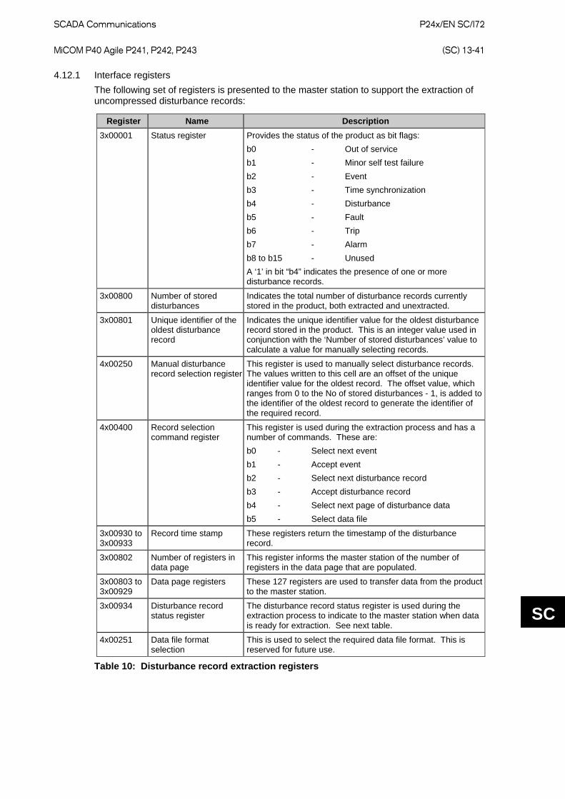
SCADA Communications
P24x/EN SC/I72 MiCOM P40 Agile P241, P242, P243 (SC) 13-41
SC
4.12.1 Interface registers The following set of registers is presented to the master station to support the extraction of uncompressed disturbance records:
Register Name Description 3x00001 Status register Provides the status of the product as bit flags:
b0 - Out of service b1 - Minor self test failure b2 - Event b3 - Time synchronization b4 - Disturbance b5 - Fault b6 - Trip b7 - Alarm b8 to b15 - Unused A ‘1’ in bit “b4” indicates the presence of one or more disturbance records.
3x00800 Number of stored disturbances
Indicates the total number of disturbance records currently stored in the product, both extracted and unextracted.
3x00801 Unique identifier of the oldest disturbance record
Indicates the unique identifier value for the oldest disturbance record stored in the product. This is an integer value used in conjunction with the ‘Number of stored disturbances’ value to calculate a value for manually selecting records.
4x00250 Manual disturbance record selection register
This register is used to manually select disturbance records. The values written to this cell are an offset of the unique identifier value for the oldest record. The offset value, which ranges from 0 to the No of stored disturbances - 1, is added to the identifier of the oldest record to generate the identifier of the required record.
4x00400 Record selection command register
This register is used during the extraction process and has a number of commands. These are: b0 - Select next event b1 - Accept event b2 - Select next disturbance record b3 - Accept disturbance record b4 - Select next page of disturbance data b5 - Select data file
3x00930 to 3x00933
Record time stamp These registers return the timestamp of the disturbance record.
3x00802 Number of registers in data page
This register informs the master station of the number of registers in the data page that are populated.
3x00803 to 3x00929
Data page registers These 127 registers are used to transfer data from the product to the master station.
3x00934 Disturbance record status register
The disturbance record status register is used during the extraction process to indicate to the master station when data is ready for extraction. See next table.
4x00251 Data file format selection
This is used to select the required data file format. This is reserved for future use.
Table 10: Disturbance record extraction registers

P24x/EN SC/I72
SCADA Communications (SC) 13-42 MiCOM P40 Agile P241, P242, P243
SC
The Disturbance Record status register reports one of the following values:
State Description Idle This is the state reported when no record is selected; such as
after power on or after a record has been marked as extracted.
Busy The product is currently processing data.
Page ready The data page has been populated and the master can now safely read the data.
Configuration complete All of the configuration data has been read without error.
Record complete 4 All of the disturbance data has been extracted.
Disturbance overwritten 5 An error occurred during the extraction process where the disturbance being extracted was overwritten by a new record.
No unextracted disturbances
6 An attempt was made by the master station to automatically select the next oldest unextracted disturbance when all records have been extracted.
Not a valid disturbance 7 An attempt was made by the master station to manually select a record that did not exist in the product.
Command out of sequence
8 The master station issued a command to the product that was not expected during the extraction process.
Table 11: Disturbance record status register (3x934) values
4.12.2 Extraction procedure The following procedure must be used to extract disturbance records from the product. The procedure is split into four sections:
1. Selection of a disturbance - either manually or automatically 2. Extraction of the configuration file 3. Extraction of the data file 4. Accepting the extracted record (automatic extraction only)
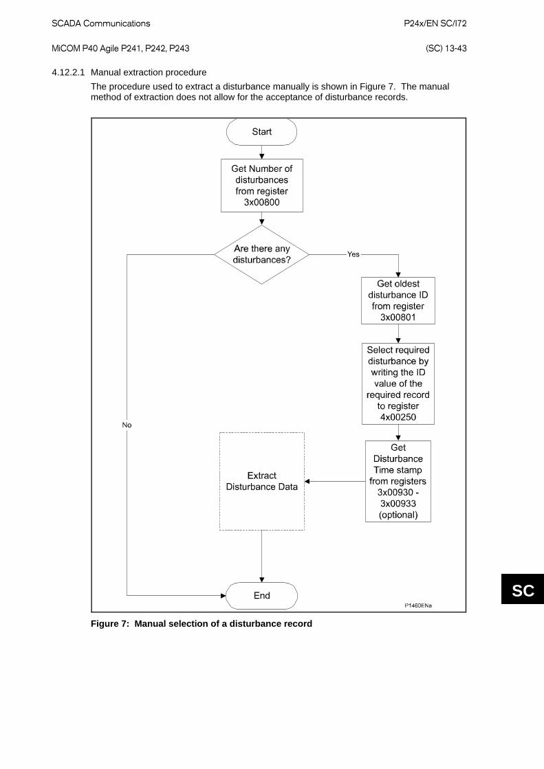
SCADA Communications
P24x/EN SC/I72 MiCOM P40 Agile P241, P242, P243 (SC) 13-43
SC
4.12.2.1 Manual extraction procedure The procedure used to extract a disturbance manually is shown in Figure 7. The manual method of extraction does not allow for the acceptance of disturbance records.
Figure 7: Manual selection of a disturbance record
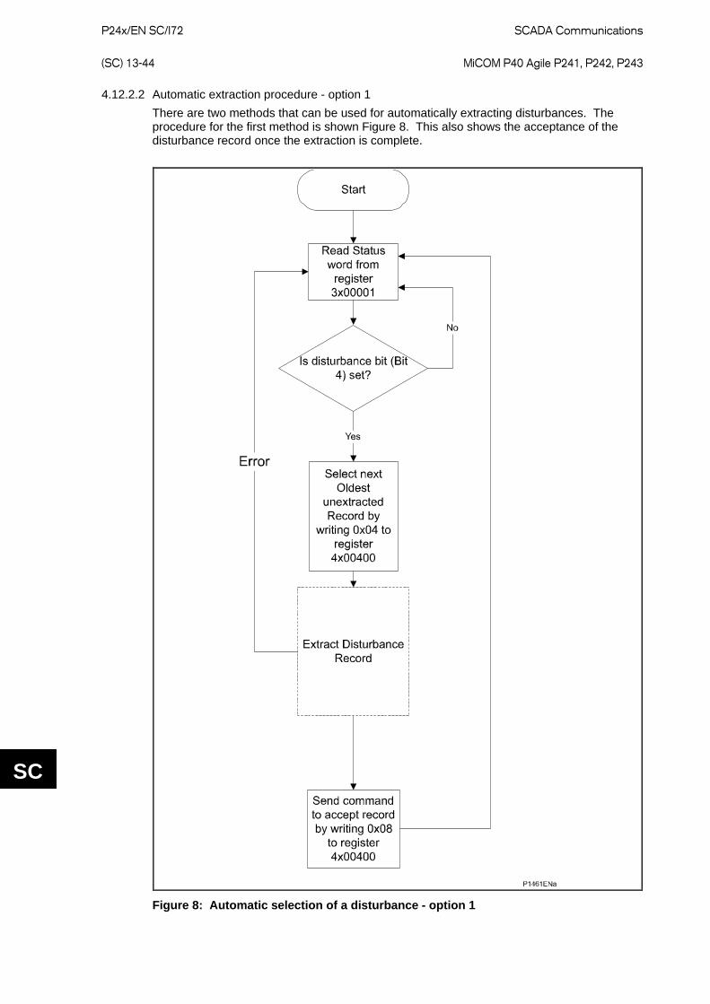
P24x/EN SC/I72
SCADA Communications (SC) 13-44 MiCOM P40 Agile P241, P242, P243
SC
4.12.2.2 Automatic extraction procedure - option 1 There are two methods that can be used for automatically extracting disturbances. The procedure for the first method is shown Figure 8. This also shows the acceptance of the disturbance record once the extraction is complete.
Figure 8: Automatic selection of a disturbance - option 1

SCADA Communications
P24x/EN SC/I72 MiCOM P40 Agile P241, P242, P243 (SC) 13-45
SC
4.12.2.3 Automatic extraction procedure - option 2 The second method that can be used for automatic extraction is shown in Figure 9. This also shows the acceptance of the disturbance record once the extraction is complete.
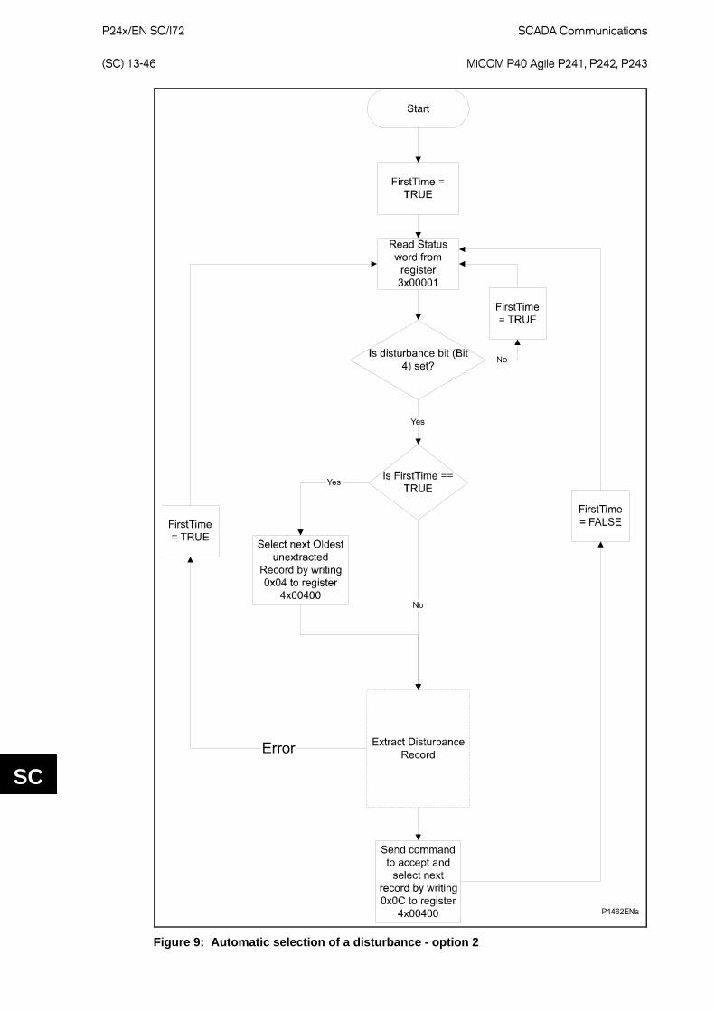
P24x/EN SC/I72
SCADA Communications (SC) 13-46 MiCOM P40 Agile P241, P242, P243
SC
Figure 9: Automatic selection of a disturbance - option 2
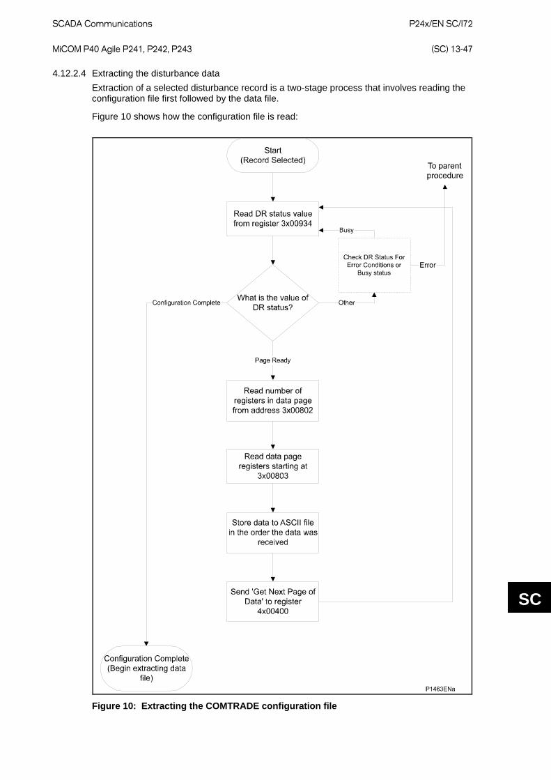
SCADA Communications
P24x/EN SC/I72 MiCOM P40 Agile P241, P242, P243 (SC) 13-47
SC
4.12.2.4 Extracting the disturbance data Extraction of a selected disturbance record is a two-stage process that involves reading the configuration file first followed by the data file.
Figure 10 shows how the configuration file is read:
Figure 10: Extracting the COMTRADE configuration file
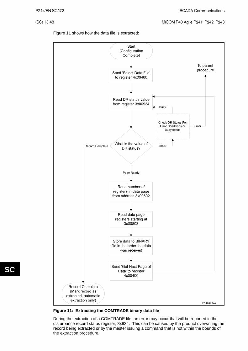
P24x/EN SC/I72
SCADA Communications (SC) 13-48 MiCOM P40 Agile P241, P242, P243
SC
Figure 11 shows how the data file is extracted:
Figure 11: Extracting the COMTRADE binary data file
During the extraction of a COMTRADE file, an error may occur that will be reported in the disturbance record status register, 3x934. This can be caused by the product overwriting the record being extracted or by the master issuing a command that is not within the bounds of the extraction procedure.
SCADA Communications
P24x/EN SC/I72 MiCOM P40 Agile P241, P242, P243 (SC) 13-49
SC
4.12.3 Storage of extracted data The extracted data needs to be written to two separate files. The first is the configuration file, which is in ASCII text format, and the second is the data file, which is in a binary format.
4.12.3.1 Storing the configuration file As the configuration data is extracted from the product, it should be stored to an ASCII text file with a ‘.cfg’ file extension. Each register in the page is a G1 format 16-bit unsigned integer that is transmitted in big-endian byte order. The master must write the configuration file page-data to the file in ascending register order with each register’s high order byte written before its low order byte, until all the pages have been processed.
4.12.3.2 Storing the binary data file As the binary data is extracted from the product, it should be stored to a binary file with the same name as the configuration file, but with a ‘.dat’ file extension instead of the ‘.cfg’ extension. Each register in the page is a G1-format 16-bit unsigned integer that is transmitted in big-endian byte order. The master must write the page data to a file in ascending register order with each register’s high order byte written before its low order byte until all the pages have been processed.
4.12.4 Disturbance record deletion All of the disturbance records stored in the product can be deleted (“cleared”) by writing 5 to the record control register 4x401 (G6 data type). See also section 4.11.4 for details about event record deletion.
4.13 Setting changes The product settings can be split into two categories:
• Control and support settings • Disturbance record settings and protection setting groups Changes to settings within the control and support area are executed immediately. Changes to the protection setting groups or the disturbance recorder settings are stored in a temporary ‘scratchpad’ area and must be confirmed before they are implemented. All the product settings are 4x page registers. The following points should be noted when changing settings:
• Settings implemented using multiple registers must be written to using a multi-register write operation. The product does not support write access to sub-parts of multi-register data types.
• The first address for a multi-register write must be a valid address. If there are unmapped addresses within the range being written to then the data associated with these addresses are discarded.
• If a write operation is performed with values that are out of range then an “illegal data” response code is produced. Valid setting values within the same write operation are executed.
• If a write operation is performed attempting to change registers that require a higher level of password access than is currently enabled then all setting changes in the write operation are discarded.
4.13.1 Password protection The product’s settings can be subject to Password protection. The level of password protection required to change a setting is indicated in the 4x register-map table in the Relay Menu Database. Level 2 is the highest level of password access, level 0 indicates that no password is required.
The following registers are available to control Password protection:
• 4x00001 & 4x00002 Password Entry • 4x00022 Default Password Level • 4x00023 & 4x00024 Setting to Change Password Level 1
P24x/EN SC/I72
SCADA Communications (SC) 13-50 MiCOM P40 Agile P241, P242, P243
SC
• 4x00025 & 4x00026 Setting to Change Password Level 2 • 3x00010 Current Access Level (read only)
4.13.2 Control and support settings Control and support settings are committed immediately when a value is written to such a register. The MODBUS registers in this category are:
• 4x00000-4x00599 • 4x00700-4x00999 • 4x02049 to 4x02052 • 4x10000-4x10999
4.13.2.1 Time synchronization The value of the product’s real time clock can be set by writing the desired time (see section 4.16) to registers 4x02049 through 4x02052. These registers are standard to General Electric MiCOM products, which facilitates the use of broadcast of a time synchronization packet -being a block write to the time setting registers sent to slave address zero.
When the product’s time has been set using these registers the Time Synchronized flag in the MODBUS Status Register (3x1: type G26) is set. The product automatically clears this flag if more than five minutes has elapsed since these registers were last written to.
A “Time synchronization” event is logged if the new time value is more than two seconds different from the current value.
4.13.3 Disturbance recorder configuration settings Disturbance recorder configuration-settings are written to a scratchpad memory area. A confirmation procedure is required to commit the contents of the scratchpad to the disturbance recorder's set-up, which ensures that the recorders configuration is consistent at all times. The contents of the scratchpad memory can be discarded with the abort procedure. The scratchpad confirmation and abort procedures are described in section 4.13.5.
The disturbance recorder configuration registers are in the range:
• 4x00600-4x00699
4.13.4 Protection settings Protection configuration-settings are written to a scratchpad memory area. A confirmation procedure is required to commit the contents of the scratchpad to the product’s protection functions, which ensures that their configuration is consistent at all times. The contents of the scratchpad memory can be discarded with the abort procedure. The scratchpad confirmation and abort procedures are described in section 4.13.5.
The product supports four groups of protection settings. One protection-group is active and the other three are either dormant or disabled. The active protection-group can be selected by writing to register 4x00404. An illegal data response is returned if an attempt is made to set the active group to one that has been disabled.
The MODBUS registers for each of the four groups are repeated in the following ranges:
• Group 1 4x01000-4x02999, 10 4x11000-4x12999 • Group 2 4x03000-4x04999, 4x13000-4x14999 • Group 3 4x05000-4x06999, 4x15000-4x16999 • Group 4 4x07000-4x08999, 4x17000-4x18999
10 Registers 4x02049 to 4x02052 are not part of protection setting group #1 and therefore do not repeat in any of the other protection setting groups. These registers are for time synchronization purposes and are standard for most General Electric products. See section 4.13.2.1.

SCADA Communications
P24x/EN SC/I72 MiCOM P40 Agile P241, P242, P243 (SC) 13-51
SC
4.13.5 Scratchpad management Register 4x00405 can be used to either confirm or abort the setting changes within the scratchpad area. In addition to the basic editing of the protection setting groups, the following functions are provided:
• Default values can be restored to a setting group or to all of the product settings by writing to register 4x00402.
• It is possible to copy the contents of one setting group to another by writing the source group to register 4x00406 and the target group to 4x00407.
• The setting changes performed by either of the two operations defined above are made to the scratchpad area. These changes must be confirmed by writing to register 4x00405.
4.14 Register data types The product maps one or more MODBUS registers to data-typed information contained within an internal database. These data-types are referred to as G-Types since they have a ‘G’ prefixed identifier. The Relay Menu Database gives a complete definition of the all of the G-Types used in the product.
In general, the data types are transmitted in high byte to low byte order, which is some times called “Big Endian format”. This may require the MODBUS master to reorder the received bytes into a format compliant with its byte-order and register order (for multi-register G-Types) conventions. Most MODBUS masters provide byte-swap and register-swap device (or data point) configuration to cope with the plethora of implementations.
The product’s data-types are atomic in nature. This means that the multi-register types cannot be read (or written) on an individual register basis. All of the registers for a multi-register data-typed item must be read (or written) with a single block read (or write) command.
The following subsections provide some additional notes for a few of the more complex G-Types.
4.15 Numeric setting (data types G2 & G35) Numeric settings are integer representations of real (non-integer) values. The register value is the number of setting increments (or steps) that the real value is away from the settings real minimum value. This is expressed by the following formula:
Sreal = Smin. + (Sinc. x Snumeric)
Where:
• Sreal - Setting real value • Smin. - Setting real minimum value • Sinc. - Setting real increment (step) value • Snumeric - Setting numeric (register) value For example, a setting with a real value setting range of 0.01 to 10 in steps of 0.01 would have the following numeric setting values:
Real value (Sreal)
Numeric value (Snumeric)
0.01 0
0.02 1
1.00 99
Table 12: Example of numeric settings
The G2 numeric data type uses 1 register as an unsigned 16-bit integer, whereas the G35 numeric data type uses 2 registers as an unsigned 32-bit integer. The G2 data type therefore provides a maximum setting range of 2^16 x Sinc. Similarly the G35 data type provides a maximum setting range of 232 x Sinc.
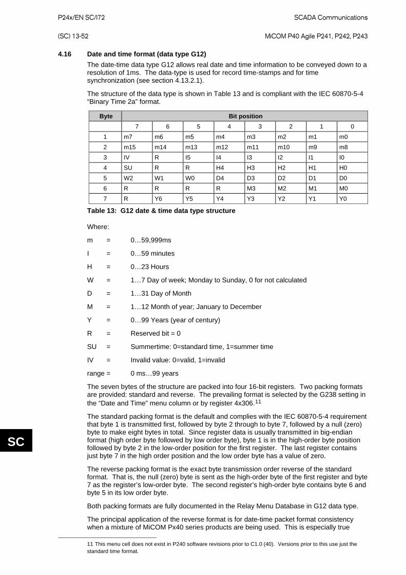
P24x/EN SC/I72
SCADA Communications (SC) 13-52 MiCOM P40 Agile P241, P242, P243
SC
4.16 Date and time format (data type G12) The date-time data type G12 allows real date and time information to be conveyed down to a resolution of 1ms. The data-type is used for record time-stamps and for time synchronization (see section 4.13.2.1).
The structure of the data type is shown in Table 13 and is compliant with the IEC 60870-5-4 “Binary Time 2a” format.
Byte Bit position 7 6 5 4 3 2 1 0
1 m7 m6 m5 m4 m3 m2 m1 m0
2 m15 m14 m13 m12 m11 m10 m9 m8
3 IV R I5 I4 I3 I2 I1 I0
4 SU R R H4 H3 H2 H1 H0
5 W2 W1 W0 D4 D3 D2 D1 D0
6 R R R R M3 M2 M1 M0
7 R Y6 Y5 Y4 Y3 Y2 Y1 Y0
Table 13: G12 date & time data type structure
Where:
m = 0…59,999ms
I = 0…59 minutes
H = 0…23 Hours
W = 1…7 Day of week; Monday to Sunday, 0 for not calculated
D = 1…31 Day of Month
M = 1…12 Month of year; January to December
Y = 0…99 Years (year of century)
R = Reserved bit = 0
SU = Summertime: 0=standard time, 1=summer time
IV = Invalid value: 0=valid, 1=invalid
range = 0 ms…99 years
The seven bytes of the structure are packed into four 16-bit registers. Two packing formats are provided: standard and reverse. The prevailing format is selected by the G238 setting in the “Date and Time” menu column or by register 4x306.11
The standard packing format is the default and complies with the IEC 60870-5-4 requirement that byte 1 is transmitted first, followed by byte 2 through to byte 7, followed by a null (zero) byte to make eight bytes in total. Since register data is usually transmitted in big-endian format (high order byte followed by low order byte), byte 1 is in the high-order byte position followed by byte 2 in the low-order position for the first register. The last register contains just byte 7 in the high order position and the low order byte has a value of zero.
The reverse packing format is the exact byte transmission order reverse of the standard format. That is, the null (zero) byte is sent as the high-order byte of the first register and byte 7 as the register’s low-order byte. The second register’s high-order byte contains byte 6 and byte 5 in its low order byte.
Both packing formats are fully documented in the Relay Menu Database in G12 data type.
The principal application of the reverse format is for date-time packet format consistency when a mixture of MiCOM Px40 series products are being used. This is especially true
11 This menu cell does not exist in P240 software revisions prior to C1.0 (40). Versions prior to this use just the standard time format.
SCADA Communications
P24x/EN SC/I72 MiCOM P40 Agile P241, P242, P243 (SC) 13-53
SC
when there is a requirement for broadcast time synchronization with a mixture of such MiCOM products.
The data type provides only the year of century value; the century must be deduced. Simplistically the century could be imposed as 20 for applications not dealing with dates stored in this format from the previous (20th) century. Alternatively, the century can be calculated as the one that produces the nearest time value to the current date. For example: 30-12-99 is 30-12-1999 when received in 1999 & 2000, but is 30-12-2099 when received in 2050. This technique allows 2 digit years to be accurately converted to 4 digits in a ±50 year window around the current datum.
The invalid bit has two applications:
1. It can indicate that the date-time information is considered inaccurate, but is the best information available.
2. Date-time information is not available. The summertime bit is used to indicate that summertime (day light saving) is being used and, more importantly, to resolve the alias and time discontinuity which occurs when summertime starts and ends. This is important for the correct time correlation of time stamped records.
Note: The value of the summertime bit does not affect the time displayed by the product).
The day of the week field is optional and if not calculated is set to zero.
This data type (and therefore the product) does not cater for time zones so the end user must determine the time zone used by the product. UTC (universal coordinated time) is commonly used and avoids the complications of daylight saving time-stamp.
4.17 Power and energy measurement data formats (G29 & G125) The power and energy measurements are available in data format G29 integer format (software version A3.1c and earlier) and the G125 IEEE754 floating point format (software A3.1d and later). The G125 format is preferred over the older G29 format.
4.17.1 Data type G29 Data type G29 consists of three registers. The first register is the per-unit power or energy measurement and is of type G28, which is a signed 16-bit quantity. The second and third registers contain a multiplier to convert the per unit value to a real value.
The multiplier is of type G27, which is an unsigned 32-bit quantity. Therefore, the overall value conveyed by the G29 data type must be calculated as G29=G28×G27.
The product calculates the G28 per unit power or energy value as G28=((measured secondary quantity) / (CT secondary) × (110 V / (VT secondary)). Since data type G28 is a signed 16-bit integer, its dynamic range is constrained to ±32768. This limitation should be borne in mind for the energy measurements, as the G29 value saturates a long time before the equivalent G125 does.
The associated G27 multiplier is calculated as G27=(CT primary) × (VT primary / 110 V) when primary value measurements are selected, and as G27=(CT secondary) × (VT secondary / 110 V) when secondary value measurements are selected.
Note: The G29 values must be read in whole multiples of three registers. It is not possible to read the G28 and G27 parts with separate read commands.
P24x/EN SC/I72
SCADA Communications (SC) 13-54 MiCOM P40 Agile P241, P242, P243
SC
Example:
For A-Phase Power (Watts) (registers 3x00300 - 3x00302) for a 110 V nominal, In = 1 A, VT ratio = 110 V:110 V and CT ratio = 1 A:1 A. Applying A-phase 1A @ 63.51V A-phase Watts = ((63.51 V × 1 A) / In=1 A) × (110/Vn=110 V) = 63.51 Watts The G28 part of the value is the truncated per unit quantity, which is equal to 64 (40h). The multiplier is derived from the VT and CT ratios set in the product, with the equation ((CT Primary) × (VT Primary) / 110 V)). Therefore, the G27 part of the value equals 1 and the overall value of the G29 register set is 64×1 = 64 W. The registers would contain: 3x00300 - 0040h 3x00301 - 0000h 3x00302 - 0001h Using the previous example with a VT ratio = 110,000 V:110 V and CT ratio = 10,000 A: 1 A the G27 multiplier would be 10,000 A×110,000 V/110 = 10,000,000. The overall value of the G29 register set is 64 × 10,000,000 = 640 MW.
Note: There is an actual error of 49 MW in this calculation due to loss of resolution.
The registers would contain: 3x00300 - 0040h 3x00301 - 0098h 3x00302 - 9680h
4.17.2 Data type G125 Data type G125 is a short float IEEE754 floating point format, which occupies 32-bits in two consecutive registers. The most significant 16-bits of the format are in the first (low order) register and the least significant 16-bits in the second register.
The value of the G125 measurement is as accurate as the product’s ability to resolve the measurement after it has applied the secondary or primary scaling factors as required. It does not suffer from the truncation errors or dynamic range limitations associated with the G29 data format.
SCADA Communications
P24x/EN SC/I72 MiCOM P40 Agile P241, P242, P243 (SC) 13-55
SC
5 IEC 60870-5-103 INTERFACE The IEC 60870-5-103 interface is a master/slave interface with the relay as the slave device. The relay conforms to compatibility level 2; compatibility level 3 is not supported.
The following IEC 60870-5-103 facilities are supported by this interface:
• Initialization (Reset) • Time Synchronization • Event Record Extraction • General Interrogation • Cyclic Measurements • General Commands • Disturbance Record Extraction • Private Codes
5.1 Physical connection and link layer Two connection options are available for IEC 60870-5-103, either the rear EIA(RS)485 port or an optional rear fiber optic port. If the fiber optic port is fitted, the active port can be selected using the front panel menu or the front Courier port. However the selection is only effective following the next relay power up.
For either of the two modes of connection it is possible to select both the relay address and baud rate using the front panel menu/front Courier. Following a change to either of these two settings a reset command is required to re-establish communications, see reset command description below.
5.2 Initialization Whenever the relay has been powered up, or if the communication parameters have been changed a reset command is required to initialize the communications. The relay responds to either of the two reset commands (Reset CU or Reset FCB), the difference being that the Reset CU clears any unsent messages in the relays transmit buffer.
The relay responds to the reset command with an identification message ASDU 5, the Cause of Transmission COT of this response is either Reset CU or Reset FCB depending on the nature of the reset command. The content of ASDU 5 is described in the IEC 60870-5-103 section of the Relay Menu Database.
In addition to ASDU 5 identification message, if the relay has been powered up it also produces a power-up event.
5.3 Time synchronization The relay time and date can be set using the time synchronization feature of the IEC 60870-5-103 protocol. The relay corrects for the transmission delay as specified in IEC 60870-5-103. If the time synchronization message is sent as a send/confirm message then the relay responds with a confirm. Whether the time-synchronization message is sent as a send/confirm or a broadcast (send/no reply) message, a time synchronization Class 1 event is generated/produced.
If the relay clock is synchronized using the IRIG-B input, it is not possible to set the relay time using the IEC 60870-5-103 interface. If the time is set using the interface, the relay creates an event with the current date and time from the internal clock, which is synchronized to IRIG-B.
5.4 Spontaneous events Events are categorized using the following information:
• Function Type • Information Number The IEC 60870-5-103 profile contains a complete listing of all events produced by the relay.
P24x/EN SC/I72
SCADA Communications (SC) 13-56 MiCOM P40 Agile P241, P242, P243
SC
5.5 General interrogation The GI request can be used to read the status of the relay, the function numbers, and information numbers that are returned during the GI cycle.
5.6 Cyclic measurements The relay produces measured values using ASDU 9 on a cyclical basis; this can be read from the relay using a Class 2 poll (note ADSU 3 is not used). The rate at which the relay produces new measured values can be controlled using the Measurement Period setting. This setting can be edited from the front panel menu/front Courier port and is active immediately following a change.
Note: The measurands transmitted by the relay are sent as a proportion of 2.4 times the rated value of the analog value.
5.7 Commands A list of the supported commands are contained in the Relay Menu Database, which is a standalone document available on request. The relay responds to other commands with an ASDU 1, with a Cause of Transmission (COT) indicating ‘negative acknowledgement’.
5.8 Test mode Using either the front panel menu or the front Courier port, it is possible to disable the relay output contacts to allow secondary injection testing to be performed. This is interpreted as ‘test mode’ by the IEC 60870-5-103 standard. An event is produced to indicate both entry to and exit from test mode. Spontaneous events and cyclic measured data transmitted while the relay is in test mode has a COT of ‘test mode’.
5.9 Disturbance records The disturbance records are stored in uncompressed format and can be extracted using the standard mechanisms described in IEC 60870-5-103.
Note: IEC 60870-5-103 only supports up to 8 records.
5.10 Blocking of monitor direction The relay supports a facility to block messages in the Monitor direction and also in the Command direction. Messages can be blocked in the Monitor and Command directions using the menu commands, Communications - CS103 Blocking - Disabled/Monitor Blocking/Command Blocking or DDB signals Monitor Blocked and Command Blocked.
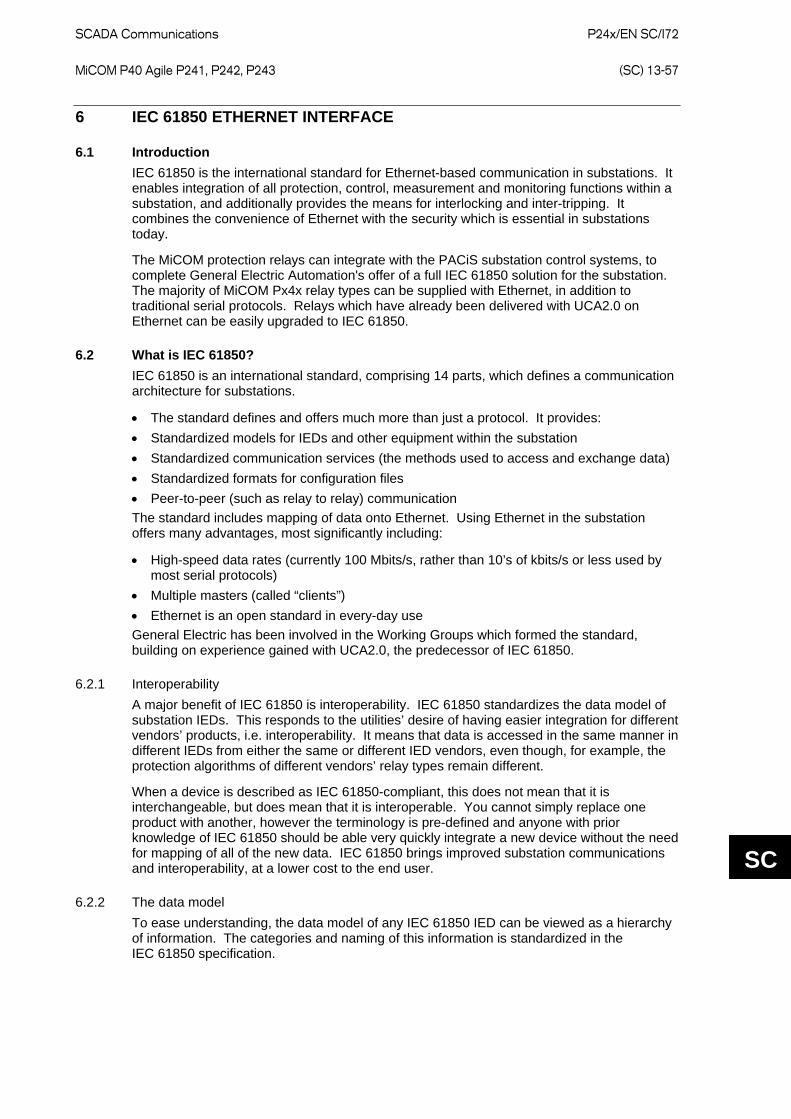
SCADA Communications
P24x/EN SC/I72 MiCOM P40 Agile P241, P242, P243 (SC) 13-57
SC
6 IEC 61850 ETHERNET INTERFACE
6.1 Introduction IEC 61850 is the international standard for Ethernet-based communication in substations. It enables integration of all protection, control, measurement and monitoring functions within a substation, and additionally provides the means for interlocking and inter-tripping. It combines the convenience of Ethernet with the security which is essential in substations today.
The MiCOM protection relays can integrate with the PACiS substation control systems, to complete General Electric Automation's offer of a full IEC 61850 solution for the substation. The majority of MiCOM Px4x relay types can be supplied with Ethernet, in addition to traditional serial protocols. Relays which have already been delivered with UCA2.0 on Ethernet can be easily upgraded to IEC 61850.
6.2 What is IEC 61850? IEC 61850 is an international standard, comprising 14 parts, which defines a communication architecture for substations.
• The standard defines and offers much more than just a protocol. It provides: • Standardized models for IEDs and other equipment within the substation • Standardized communication services (the methods used to access and exchange data) • Standardized formats for configuration files • Peer-to-peer (such as relay to relay) communication The standard includes mapping of data onto Ethernet. Using Ethernet in the substation offers many advantages, most significantly including:
• High-speed data rates (currently 100 Mbits/s, rather than 10’s of kbits/s or less used by most serial protocols)
• Multiple masters (called “clients”) • Ethernet is an open standard in every-day use General Electric has been involved in the Working Groups which formed the standard, building on experience gained with UCA2.0, the predecessor of IEC 61850.
6.2.1 Interoperability A major benefit of IEC 61850 is interoperability. IEC 61850 standardizes the data model of substation IEDs. This responds to the utilities’ desire of having easier integration for different vendors’ products, i.e. interoperability. It means that data is accessed in the same manner in different IEDs from either the same or different IED vendors, even though, for example, the protection algorithms of different vendors’ relay types remain different.
When a device is described as IEC 61850-compliant, this does not mean that it is interchangeable, but does mean that it is interoperable. You cannot simply replace one product with another, however the terminology is pre-defined and anyone with prior knowledge of IEC 61850 should be able very quickly integrate a new device without the need for mapping of all of the new data. IEC 61850 brings improved substation communications and interoperability, at a lower cost to the end user.
6.2.2 The data model To ease understanding, the data model of any IEC 61850 IED can be viewed as a hierarchy of information. The categories and naming of this information is standardized in the IEC 61850 specification.
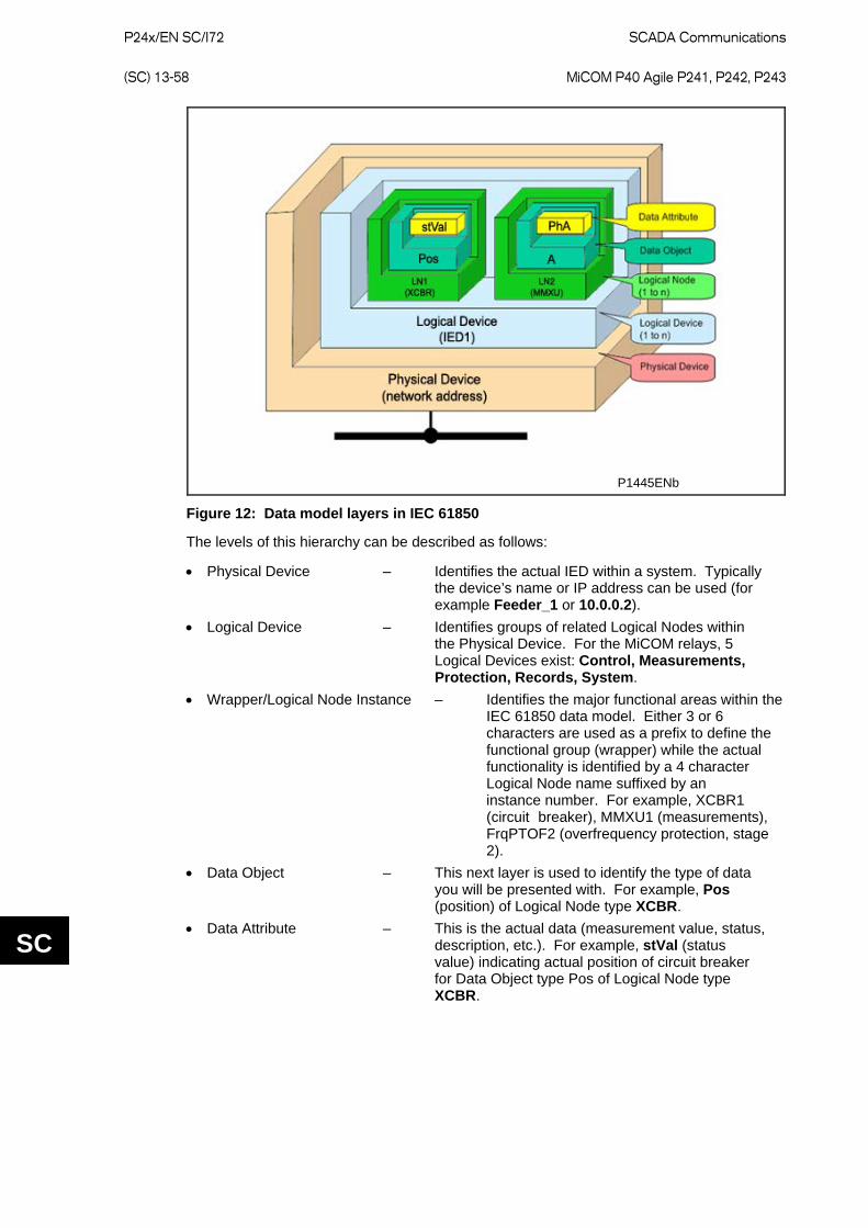
P24x/EN SC/I72
SCADA Communications (SC) 13-58 MiCOM P40 Agile P241, P242, P243
SC
P1445ENb
Figure 12: Data model layers in IEC 61850
The levels of this hierarchy can be described as follows:
• Physical Device – Identifies the actual IED within a system. Typically the device’s name or IP address can be used (for example Feeder_1 or 10.0.0.2).
• Logical Device – Identifies groups of related Logical Nodes within the Physical Device. For the MiCOM relays, 5 Logical Devices exist: Control, Measurements, Protection, Records, System.
• Wrapper/Logical Node Instance – Identifies the major functional areas within the IEC 61850 data model. Either 3 or 6 characters are used as a prefix to define the functional group (wrapper) while the actual functionality is identified by a 4 character Logical Node name suffixed by an instance number. For example, XCBR1 (circuit breaker), MMXU1 (measurements), FrqPTOF2 (overfrequency protection, stage 2).
• Data Object – This next layer is used to identify the type of data you will be presented with. For example, Pos (position) of Logical Node type XCBR.
• Data Attribute – This is the actual data (measurement value, status, description, etc.). For example, stVal (status value) indicating actual position of circuit breaker for Data Object type Pos of Logical Node type XCBR.
SCADA Communications
P24x/EN SC/I72 MiCOM P40 Agile P241, P242, P243 (SC) 13-59
SC
6.3 IEC 61850 in MiCOM relays IEC 61850 is implemented in MiCOM relays by use of a separate Ethernet card. This card manages the majority of the IEC 61850 implementation and data transfer to avoid any impact on the performance of the protection.
To communicate with an IEC 61850 IED on Ethernet, it is necessary only to know its IP address. This can then be configured into either:
• An IEC 61850 client (or master), for example a PACiS computer (MiCOM C264) or HMI, or
• An MMS browser, with which the full data model can be retrieved from the IED, without any prior knowledge
6.3.1 Capability The IEC 61850 interface provides the following capabilities:
1. Read access to measurements All measurands are presented using the measurement Logical Nodes, in the ‘Measurements’ Logical Device. Reported measurement values are refreshed by the relay once per second, in line with the relay user interface.
2. Generation of unbuffered reports on change of status/measurement Unbuffered reports, when enabled, report any change of state in statuses and/or measurements (according to deadband settings).
3. Support for time synchronization over an Ethernet link Time synchronization is supported using SNTP (Simple Network Time Protocol); this protocol is used to synchronize the internal real time clock of the relays.
4. GOOSE peer-to-peer communication GOOSE communications of statuses are included as part of the IEC 61850 implementation. Please see section 6.6 for more details.
5. Disturbance record extraction Extraction of disturbance records, by file transfer, is supported by the MiCOM relays. The record is extracted as an ASCII format COMTRADE file.
6. Controls The following control services are available:
• Direct Control • Direct Control with enhanced security • Select Before Operate (SBO) with enhanced security Controls shall be applied to open and close circuit breakers via XCBR.Pos and DDB signals ‘Control Trip’ and ‘Control Close’.
System/LLN0. LLN0.LEDRs shall be used to reset any trip LED indications.
7. Reports Reports only include data objects that have changed and not the complete dataset. The exceptions to this are a General Interrogation request and integrity reports.
• Buffered Reports Eight Buffered Report Control Blocks, (BRCB), are provided in SYSTEM/LLN0 in Logical Device ‘System’
Buffered reports are configurable to use any configurable dataset located in the same Logical device as the BRCB (i.e. SYSTEM/LLN0)
• Unbuffered Reports Sixteen Unbuffered Report Control Blocks, (URCB) are provided in SYSTEM/LLN0 in Logical Device ‘System’
P24x/EN SC/I72
SCADA Communications (SC) 13-60 MiCOM P40 Agile P241, P242, P243
SC
Unbuffered reports are configurable to use any configurable dataset located in the same Logical device as the URCB (i.e. SYSTEM/LLN0)
8. Configurable Data Sets It is possible to create and configure datasets in any Logical Node using the IED Configurator. The maximum number of datasets is specified in an IEDs ICD file. An IED is capable of handling 100 datasets.
9. Published GOOSE message Eight GOCBs are provided in SYSTEM/LLN0.
10. Uniqueness of control Uniqueness of control mechanism is implemented in the P24x to have consistency with the PACiS mechanism. This requires the relay to subscribe to the OrdRun signal from all devices in the system and be able to publish such a signal in a GOOSE message.
11. Select Active Setting Group Functional protection groups can be enabled or disabled using private mod/beh attributes in Protection/LLN0.OcpMod object. Setting groups are selectable using the Setting Group Control Block class, (SGCB). The Active Setting Group can be selected using the System/LLN0.SP.SGCB.ActSG data attribute in Logical Device ‘System’.
12. Quality for GOOSE It is possible to process the quality attributes of any Data Object in an incoming GOOSE message. Devices that do not support IEC 61850 Quality flags shall send quality attributes as all zeros.
13. Address List An Address List document (to be titled ADL) is produced for each IED which shows the mapping between the IEC 61850 data model and the internal data model of the IED. It includes a mapping in the reverse direction, which may be more useful. This document is separate from the PICS/MICS document.
14. Originator of Control Originator of control mechanism is implemented for operate response message and in the data model on the ST of the related control object, consistent with the PACiS mechanism.
Setting changes (such as protection settings) are not supported in the current IEC 61850 implementation. To keep this process as simple as possible, such setting changes are done using MiCOM S1 Studio Settings & Records program. This can be done as previously using the front port serial connection of the relay, or now optionally over the Ethernet link if preferred (this is known as “tunneling”).
6.3.2 IEC 61850 configuration One of the main objectives of IEC 61850 is to allow IEDs to be directly configured from a configuration file generated at system configuration time. At the system configuration level, the capabilities of the IED are determined from an IED capability description file (ICD) which is provided with the product. Using a collection of these ICD files from varying products, the entire protection of a substation can be designed, configured and tested (using simulation tools) before the product is even installed into the substation.
To aid in this process, the MiCOM S1 Studio Support Software provides an IED Configurator tool which allows the pre-configured IEC 61850 configuration file (an SCD file or CID file) to be imported and transferred to the IED. Alongside this, the requirements of manual configuration are satisfied by allowing the manual creation of configuration files for MiCOM relays based on their original IED capability description (ICD file).
Other features include the extraction of configuration data for viewing and editing, and a sophisticated error checking sequence which ensures that the configuration data is valid for sending to the IED and that the IED functions in the context of the substation.
To aid the user, some configuration data is available in the IED CONFIGURATOR column of the relay user interface, allowing read-only access to basic configuration data.
SCADA Communications
P24x/EN SC/I72 MiCOM P40 Agile P241, P242, P243 (SC) 13-61
SC
6.3.2.1 Configuration banks To promote version management and minimize down-time during system upgrades and maintenance, the MiCOM relays have incorporated a mechanism consisting of multiple configuration banks. These configuration banks are categorized as:
• Active Configuration Bank • Inactive Configuration Bank Any new configuration sent to the relay is automatically stored into the inactive configuration bank, therefore not immediately affecting the current configuration. Both active and inactive configuration banks can be extracted at anytime.
When the upgrade or maintenance stage is complete, the IED Configurator tool can be used to transmit a command (to a single IED) authorizing the activation of the new configuration contained in the inactive configuration bank, by switching the active and inactive configuration banks. This technique ensures that the system down-time is minimized to the start-up time of the new configuration. The capability to switch the configuration banks is also available using the IED CONFIGURATOR column.
For version management, data is available in the IED CONFIGURATOR column in the relay user interface, displaying the SCL Name and Revision attributes of both configuration banks.
6.3.2.2 Network connectivity
Note: This section presumes a prior knowledge of IP addressing and related topics. Further details on this topic may be found on the Internet (search for IP Configuration) and in numerous relevant books.
Configuration of the relay IP parameters (IP Address, Subnet Mask, Gateway) and SNTP time synchronization parameters (SNTP Server 1, SNTP Server 2) is performed by the IED Configurator tool, so if these parameters are not available using an SCL file, they must be configured manually.
If the assigned IP address is duplicated elsewhere on the same network, the remote communications operates in an indeterminate way. However, the relay will check for a conflict on every IP configuration change and at power up. An alarm is raised if an IP conflict is detected.
The relay can be configured to accept data from networks other than the local network by using the ‘Gateway’ setting.
6.4 The data model of MiCOM relays The data model naming adopted in the Px40 relays has been standardized for consistency. Therefore, the Logical Nodes are allocated to one of the five Logical Devices, as appropriate, and the wrapper names used to instantiate Logical Nodes are consistent between Px40 relays.
The data model is described in the Model Implementation Conformance Statement (MICS) document, which is available separately. The MICS document provides lists of Logical Device definitions, Logical Node definitions, Common Data Class and Attribute definitions, Enumeration definitions, and MMS data type conversions. It generally follows the format used in Parts 7-3 and 7-4 of the IEC 61850 standard.
6.5 The communication services of MiCOM relays The IEC 61850 communication services which are implemented in the Px40 relays are described in the Protocol Implementation Conformance Statement (PICS) document, which is available separately. The PICS document provides the Abstract Communication Service Interface (ACSI) conformance statements as defined in Annex A of Part 7-2 of the IEC 61850 standard.
P24x/EN SC/I72
SCADA Communications (SC) 13-62 MiCOM P40 Agile P241, P242, P243
SC
6.6 Peer-to-peer (GSE) communications The implementation of IEC 61850 Generic Substation Event (GSE) sets the way for cheaper and faster inter-relay communications. The generic substation event model provides the possibility for a fast and reliable system-wide distribution of input and output data values. The generic substation event model is based on the concept of an autonomous decentralization, providing an efficient method allowing the simultaneous delivery of the same generic substation event information to more than one physical device through the use of multicast services.
The use of multicast messaging means that IEC 61850 GOOSE uses a publisher-subscriber system to transfer information around the network*. When a device detects a change in one of its monitored status points it publishes (i.e. sends) a new message. Any device that is interested in the information subscribes (i.e. listens) to the data it contains.
Note: * Multicast messages cannot be routed across networks without specialized equipment.
Each new message is re-transmitted at user-configurable intervals until the maximum interval is reached, to overcome possible corruption due to interference, and collisions. In practice, the parameters which control the message transmission cannot be calculated. Time must be allocated to the testing of GSE schemes before or during commissioning, in just the same way a hardwired scheme must be tested.
6.6.1 Scope A maximum of 64 virtual inputs are available within the PSL which can be mapped directly to a published dataset in a GOOSE message (Configurable dataset is supported).
Each GOOSE signal contained in a subscribed GOOSE message can be mapped to any of the 64 virtual inputs within the PSL. The virtual inputs allow the mapping to internal logic functions for protection control, directly to output contacts or LEDs for monitoring.
The MiCOM relay can subscribe to all GOOSE messages but only the following data types can be decoded and mapped to a virtual input:
• BOOLEAN • BSTR2 • INT16 • INT32 • INT8 • UINT16 • UINT32 • UINT8
6.6.2 IEC 61850 GOOSE configuration All GOOSE configuration is performed using the IED Configurator tool available in the MiCOM S1 Studio Support Software.
All GOOSE publishing configuration can be found under the ‘GOOSE Publishing’ tab in the configuration editor window. All GOOSE subscription configuration can be found under the ‘GOOSE SUBSCRIBE’ tab in the configuration editor window. Care should be taken to ensure that the configuration is correct, to ensure efficient GOOSE scheme operation.
Settings to enable GOOSE signaling and to apply Test Mode are available via the relay user interface.
6.7 Ethernet functionality Settings relating to a failed Ethernet link are available in the COMMUNICATIONS column of the relay user interface.
SCADA Communications
P24x/EN SC/I72 MiCOM P40 Agile P241, P242, P243 (SC) 13-63
SC
6.7.1 Ethernet disconnection IEC 61850 ‘Associations’ are unique and made to the relay between the client (master) and server (IEC 61850 device). In the event that the Ethernet is disconnected, such associations are lost, and need to be re-established by the client. The TCP_KEEPALIVE function is implemented in the relay to monitor each association, and terminate any which are no longer active.
6.7.2 Redundant Ethernet communication ports For information regarding the Redundant Ethernet communication ports, refer to the stand alone document Px4x/EN REB/B11.
6.7.3 Loss of power The relay allows the re-establishment of associations by the client without a negative impact on the relay’s operation after having its power removed. As the relay acts as a server in this process, the client must request the association. Uncommitted settings are cancelled when power is lost, and reports requested by connected clients are reset and must be re-enabled by the client when it next creates the new association to the relay.
P24x/EN SC/I72
SCADA Communications (SC) 13-64 MiCOM P40 Agile P241, P242, P243
SC
7 SECOND REAR COMMUNICATIONS PORT (COURIER) Relays with Courier, MODBUS or IEC 60870-5-103 protocol on the first rear communications port have the option of a second rear port, running the Courier language. The second port is designed typically for dial-up modem access by protection engineers/operators, when the main port is reserved for SCADA communication traffic. Communication is via one of three physical links: K-Bus, EIA(RS)485 or EIA(RS)2321. The port supports full local or remote protection and control access by MiCOM S1 Studio software.
When changing the port configuration between K-Bus, EIA(RS)485 and EIA(RS)232 it is necessary to reboot the relay to update the hardware configuration of the second rear port. There is also provision for the EIA(RS)485 and EIA(RS)232 protocols to be configured to operate with a modem, using an IEC 60870 10 bit frame.
Port configuration Valid communication protocol K-Bus K-Bus
EIA(RS)232 IEC 60870 FT1.2, 11-bit frame IEC 60870, 10-bit frame
EIA(RS)485 IEC 60870 FT1.2, 11-bit frame IEC 60870, 10-bit frame
Table 14: Available physical links and their corresponding valid protocols
If both rear communications ports are connected to the same bus, care should be taken to ensure their address settings are not the same, to avoid message conflicts.
7.1 Courier protocol The following documentation should be referred to for a detailed description of the Courier protocol, command set and link description.
• R6509 K-Bus Interface Guide • R6510 IEC 60870 Interface Guide • R6511 Courier Protocol • R6512 Courier User Guide The second rear communications port is functionally the same as detailed in section 2.2 for a Courier rear communications port, with the following exceptions:
7.2 Event extraction Automatic event extraction is not supported when the first rear port protocol is Courier, MODBUS or CS103.
7.3 Disturbance record extraction Automatic disturbance record extraction is not supported when the first rear port protocol is Courier, MODBUS or CS103.
7.4 Connection to the second rear port The second rear Courier port connects via the 9-way female D-type connector (SK4) in the middle of the card end plate (in between IRIG-B connector and lower D-type). The connection is compliant to EIA(RS)574.
For IEC 60870-5-2 over EIA(RS)232.
Pin Connection 1 No Connection
2 RxD
3 TxD
4 DTR#
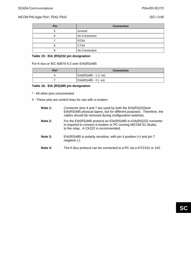
SCADA Communications
P24x/EN SC/I72 MiCOM P40 Agile P241, P242, P243 (SC) 13-65
SC
Pin Connection 5 Ground
6 No Connection
7 RTS#
8 CTS#
9 No Connection
Table 15: EIA (RS)232 pin designation
For K-bus or IEC 60870-5-2 over EIA(RS)485
Pin* Connection 4 EIA(RS)485 - 1 (+ ve)
7 EIA(RS)485 - 2 (- ve)
Table 16: EIA (RS)485 pin designation
* - All other pins unconnected.
# - These pins are control lines for use with a modem.
Note 1: Connector pins 4 and 7 are used by both the EIA(RS)232and EIA(RS)485 physical layers, but for different purposes. Therefore, the cables should be removed during configuration switches.
Note 2: For the EIA(RS)485 protocol an EIA(RS)485 to EIA(RS)232 converter is required to connect a modem or PC running MiCOM S1 Studio, to the relay. A CK222 is recommended.
Note 3: EIA(RS)485 is polarity sensitive, with pin 4 positive (+) and pin 7 negative (-).
Note 4: The K-Bus protocol can be connected to a PC via a KITZ101 or 102.

P24x/EN SC/I72
SCADA Communications (SC) 13-66 MiCOM P40 Agile P241, P242, P243
SC
8 SK5 PORT CONNECTION The lower 9-way D-type connector (SK5) is currently unsupported. Do not connect to this port.

Symbols and Glossary
P24x/EN SG/I72 MiCOM P40 Agile P241, P242, P243 (SG) 14-1
SG
SYMBOLS AND GLOSSARY

P24x/EN SG/I72
Symbols and Glossary (SG) 4-2 MiCOM P40 Agile P241, P242, P243
SG

Symbols and Glossary
P24x/EN SG/I72 MiCOM P40 Agile P241, P242, P243 (SG) 14-3
SG
TABLES Table 1: List of principle symbols 10
Table 2: Logic timers 12
Table 3: Logic gates 13

P24x/EN SG/I72
Symbols and Glossary (SG) 4-4 MiCOM P40 Agile P241, P242, P243
SG
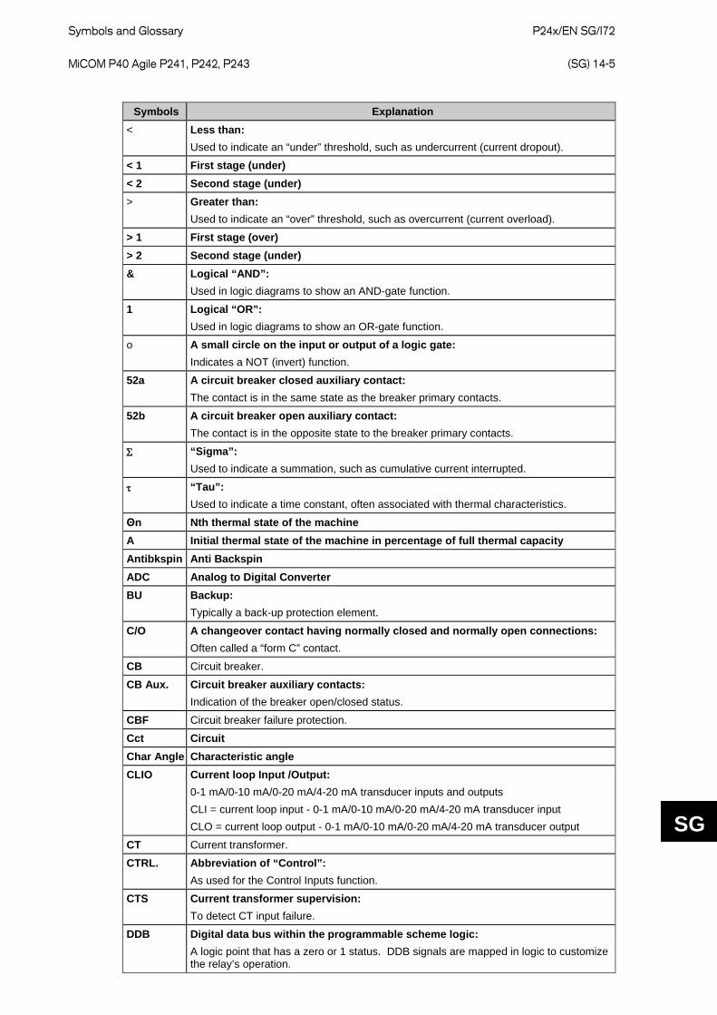
Symbols and Glossary
P24x/EN SG/I72 MiCOM P40 Agile P241, P242, P243 (SG) 14-5
SG
Symbols Explanation
< Less than: Used to indicate an “under” threshold, such as undercurrent (current dropout).
< 1 First stage (under) < 2 Second stage (under) > Greater than:
Used to indicate an “over” threshold, such as overcurrent (current overload).
> 1 First stage (over) > 2 Second stage (under) & Logical “AND”:
Used in logic diagrams to show an AND-gate function.
1 Logical “OR”: Used in logic diagrams to show an OR-gate function.
o A small circle on the input or output of a logic gate: Indicates a NOT (invert) function.
52a A circuit breaker closed auxiliary contact: The contact is in the same state as the breaker primary contacts.
52b A circuit breaker open auxiliary contact: The contact is in the opposite state to the breaker primary contacts.
Σ “Sigma”: Used to indicate a summation, such as cumulative current interrupted.
τ “Tau”: Used to indicate a time constant, often associated with thermal characteristics.
Θn Nth thermal state of the machine A Initial thermal state of the machine in percentage of full thermal capacity Antibkspin Anti Backspin ADC Analog to Digital Converter BU Backup:
Typically a back-up protection element.
C/O A changeover contact having normally closed and normally open connections: Often called a “form C” contact.
CB Circuit breaker.
CB Aux. Circuit breaker auxiliary contacts: Indication of the breaker open/closed status.
CBF Circuit breaker failure protection.
Cct Circuit Char Angle Characteristic angle CLIO Current loop Input /Output:
0-1 mA/0-10 mA/0-20 mA/4-20 mA transducer inputs and outputs CLI = current loop input - 0-1 mA/0-10 mA/0-20 mA/4-20 mA transducer input CLO = current loop output - 0-1 mA/0-10 mA/0-20 mA/4-20 mA transducer output
CT Current transformer.
CTRL. Abbreviation of “Control”: As used for the Control Inputs function.
CTS Current transformer supervision: To detect CT input failure.
DDB Digital data bus within the programmable scheme logic: A logic point that has a zero or 1 status. DDB signals are mapped in logic to customize the relay’s operation.
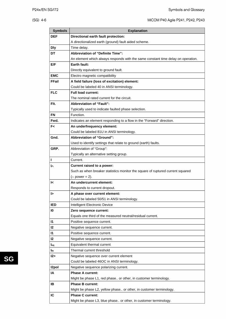
P24x/EN SG/I72
Symbols and Glossary (SG) 4-6 MiCOM P40 Agile P241, P242, P243
SG
Symbols Explanation DEF Directional earth fault protection:
A directionalized earth (ground) fault aided scheme.
Dly Time delay.
DT Abbreviation of “Definite Time”: An element which always responds with the same constant time delay on operation.
E/F Earth fault: Directly equivalent to ground fault.
EMC Electro magnetic compatibility
FFail A field failure (loss of excitation) element: Could be labeled 40 in ANSI terminology.
FLC Full load current: The nominal rated current for the circuit.
Flt. Abbreviation of “Fault”: Typically used to indicate faulted phase selection.
FN Function.
Fwd. Indicates an element responding to a flow in the “Forward” direction.
F< An underfrequency element: Could be labeled 81U in ANSI terminology.
Gnd. Abbreviation of “Ground”: Used to identify settings that relate to ground (earth) faults.
GRP. Abbreviation of “Group”: Typically an alternative setting group.
I Current.
I∧ Current raised to a power: Such as when breaker statistics monitor the square of ruptured current squared (∧ power = 2).
I< An undercurrent element: Responds to current dropout.
I> A phase over current element: Could be labeled 50/51 in ANSI terminology.
IED Intelligent Electronic Device
I0 Zero sequence current: Equals one third of the measured neutral/residual current.
I1 Positive sequence current.
I2 Negative sequence current.
I1 Positive sequence current.
I2 Negative sequence current.
Ieq Equivalent thermal current
Ith Thermal current threshold
I2> Negative sequence over current element Could be labeled 46OC in ANSI terminology.
I2pol Negative sequence polarizing current.
IA Phase A current: Might be phase L1, red phase.. or other, in customer terminology.
IB Phase B current: Might be phase L2, yellow phase.. or other, in customer terminology.
IC Phase C current: Might be phase L3, blue phase.. or other, in customer terminology.

Symbols and Glossary
P24x/EN SG/I72 MiCOM P40 Agile P241, P242, P243 (SG) 14-7
SG
Symbols Explanation ID Abbreviation of “Identifier”:
Often a label used to track a software version installed.
IDMT Inverse definite minimum time: A characteristic whose trip time depends on the measured input (e.g. current) according to an inverse-time curve.
In The rated nominal current of the relay: Software selectable as 1 amp or 5 amp to match the line CT input.
IN Neutral current, or residual current: This results from an internal summation of the three measured phase currents.
IN> A neutral (residual) over current element: Detects earth (ground) faults. Could be labeled 50N/51N in ANSI terminology.
Inh An inhibit signal.
ISEF> A sensitive Earth Fault over current element: Detects earth (ground) faults. Could be labeled 50N/51N in ANSI terminology.
Inst. An element with “instantaneous” operation: i.e. having no deliberate time delay.
I/O Abbreviation of “Inputs and Outputs”: Used in connection with the number of opto coupled inputs and output contacts within the relay.
I/P Abbreviation of “Input”.
K Thermal coefficient
LCD Liquid crystal display: The front-panel text display on the relay.
LD Abbreviation of “Level Detector”: An element responding to a current or voltage below its set threshold.
LED Light emitting diode: Red or green indicator on the relay front-panel.
MCB A “miniature circuit breaker”: Used instead of a fuse to protect VT secondary circuits.
Mot Diff A motor differential element: Could be labeled 87 in ANSI terminology.
N Indication of “Neutral” involvement in a fault: i.e. a ground (earth) fault.
Nb Number N/A Not applicable.
N/C A normally closed or “break” contact: Often called a “form B” contact.
NLR Non Linear Resistor (Metrosil)
N/O A normally open or “make” contact: Often called a “form A” contact.
NPS Negative phase sequence.
NXT Abbreviation of “Next”: In connection with hotkey menu navigation.
NVD Neutral voltage displacement: Equivalent to residual over voltage protection.
O/P Abbreviation of “output”.
Opto An opto coupled logic input: Alternative terminology: binary input.
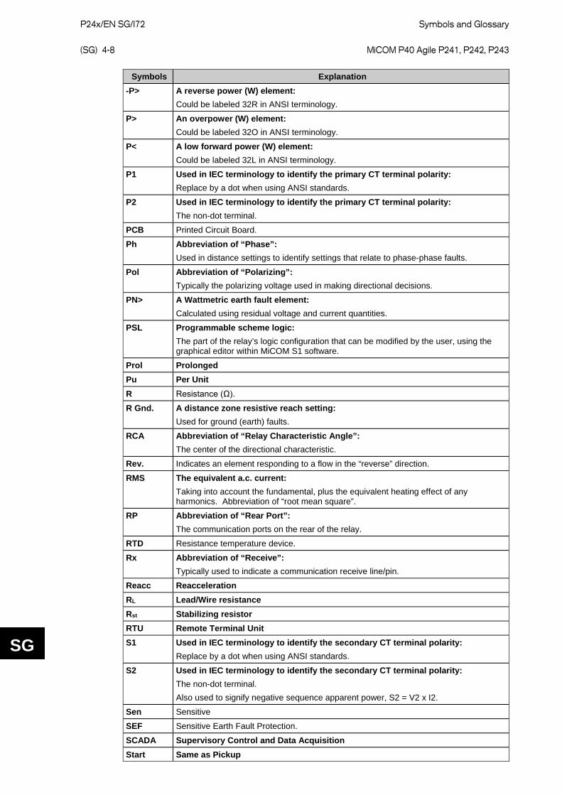
P24x/EN SG/I72
Symbols and Glossary (SG) 4-8 MiCOM P40 Agile P241, P242, P243
SG
Symbols Explanation -P> A reverse power (W) element:
Could be labeled 32R in ANSI terminology.
P> An overpower (W) element: Could be labeled 32O in ANSI terminology.
P< A low forward power (W) element: Could be labeled 32L in ANSI terminology.
P1 Used in IEC terminology to identify the primary CT terminal polarity: Replace by a dot when using ANSI standards.
P2 Used in IEC terminology to identify the primary CT terminal polarity: The non-dot terminal.
PCB Printed Circuit Board.
Ph Abbreviation of “Phase”: Used in distance settings to identify settings that relate to phase-phase faults.
Pol Abbreviation of “Polarizing”: Typically the polarizing voltage used in making directional decisions.
PN> A Wattmetric earth fault element: Calculated using residual voltage and current quantities.
PSL Programmable scheme logic: The part of the relay’s logic configuration that can be modified by the user, using the graphical editor within MiCOM S1 software.
Prol Prolonged Pu Per Unit R Resistance (Ω).
R Gnd. A distance zone resistive reach setting: Used for ground (earth) faults.
RCA Abbreviation of “Relay Characteristic Angle”: The center of the directional characteristic.
Rev. Indicates an element responding to a flow in the “reverse” direction.
RMS The equivalent a.c. current: Taking into account the fundamental, plus the equivalent heating effect of any harmonics. Abbreviation of “root mean square”.
RP Abbreviation of “Rear Port”: The communication ports on the rear of the relay.
RTD Resistance temperature device.
Rx Abbreviation of “Receive”: Typically used to indicate a communication receive line/pin.
Reacc Reacceleration RL Lead/Wire resistance Rst Stabilizing resistor RTU Remote Terminal Unit S1 Used in IEC terminology to identify the secondary CT terminal polarity:
Replace by a dot when using ANSI standards.
S2 Used in IEC terminology to identify the secondary CT terminal polarity: The non-dot terminal. Also used to signify negative sequence apparent power, S2 = V2 x I2.
Sen Sensitive
SEF Sensitive Earth Fault Protection.
SCADA Supervisory Control and Data Acquisition Start Same as Pickup

Symbols and Glossary
P24x/EN SG/I72 MiCOM P40 Agile P241, P242, P243 (SG) 14-9
SG
Symbols Explanation t A time delay.
T Ambient temperature in degrees Celsius
T1 Thermal characteristic time constant during over load
T2 Thermal characteristic time constant during start up period
Tr Thermal characteristic time constant during cooling down period (stopping)
top Operating time
tn Elapsed time often used in comparison with a set time
TCS Trip circuit supervision.
TD The time dial multiplier setting: Applied to inverse-time curves (ANSI/IEEE).
TE A standard for measuring the width of a relay case: One inch = 5TE units.
Thermal I> A stator thermal overload element: Could be labeled 49 in ANSI terminology.
TMS The time multiplier setting applied to inverse-time curves (IEC).
Tx Abbreviation of “Transmit”: Typically used to indicate a communication transmit line/pin.
V Voltage.
V< An undervoltage element: Could be labeled 27 in ANSI terminology.
V> An overvoltage element: Could be labeled 59 in ANSI terminology.
V0 Zero sequence voltage: Equals one third of the measured neutral/residual voltage.
V1 Positive sequence voltage.
V2 Negative sequence voltage.
V2> A negative phase sequence (NPS) over voltage element: Could be labeled 47 in ANSI terminology.
V2pol Negative sequence polarizing voltage.
VA Phase A voltage: Might be phase L1, red phase.. or other, in customer terminology.
VB Phase B voltage: Might be phase L2, yellow phase.. or other, in customer terminology.
VC Phase C voltage: Might be phase L3, blue phase.. or other, in customer terminology.
Vk IEC knee point voltage of a current transformer.
Vn The rated nominal voltage of the relay: To match the line VT input.
VN Neutral voltage displacement, or residual voltage.
VN> A residual (neutral) over voltage element: Could be labeled 59N in ANSI terminology.
Vrem. Remanent voltage, phase to phase measurement, connected on the Motor side, used in Antibackspin protection.
Vres. Neutral voltage displacement, or residual voltage.
Vr Residual voltage- Voltage output of an open delta VT secondary
Vs Voltage setting used for high impedance differential protection
VT Voltage transformer.

P24x/EN SG/I72
Symbols and Glossary (SG) 4-10 MiCOM P40 Agile P241, P242, P243
SG
Symbols Explanation Vx An auxiliary supply voltage:
Typically the substation battery voltage used to power the relay.
Z< An under impedance element: Could be labeled 21 in ANSI terminology.
Z0 Zero sequence impedance.
Z1 Positive sequence impedance.
Z2 Negative sequence impedance.
Table 1: List of principle symbols
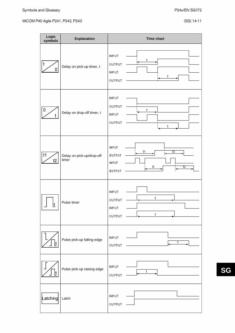
Symbols and Glossary
P24x/EN SG/I72 MiCOM P40 Agile P241, P242, P243 (SG) 14-11
SG
Logic
symbols Explanation Time chart
Delay on pick-up timer, t
Delay on drop-off timer, t
Delay on pick-up/drop-off timer
Pulse timer
Pulse pick-up falling edge
Pulse pick-up raising edge
Latch

P24x/EN SG/I72
Symbols and Glossary (SG) 4-12 MiCOM P40 Agile P241, P242, P243
SG
Logic symbols Explanation Time chart
Dwell timer
Straight (non latching): Hold value until input reset signal
Table 2: Logic timers

Symbols and Glossary
P24x/EN SG/I72 MiCOM P40 Agile P241, P242, P243 (SG) 14-13
SG
V02400
AND GATESymbol Truth Table Symbol Truth Table Symbol Truth Table
AB Y A
B Y&A B Y
00 00 0
001
11 1 1
IN OUTA B Y
00 00
001
11 1
1
0
IN OUTA B Y0 00
01
11 1
1
0
1
1& A
B Y&
IN OUT
OR GATESymbol Symbol Symbol Truth TableTruth TableTruth Table
1AB Y A
B Y1 AB Y1
1 11
IN OUTA B Y
00 00
01
111
1 11
IN OUTA B Y
10 00
01
110 1 01
A B Y10 0
001
100
S – R FLIP-FLOPSymbol Symbol SymbolTruth Table Truth Table Truth Table
RS
QAB Y R
SDQ
AB Y RDB
SQ
AY
RD = ResetDominant
A B Q0 Q10 0 0 00 1
1
00
11
0
0
0
0
0
111
1
11
11
0
01
0110
1
A B Q0 Q10 0 0 00
1
1
1
01
10
0
0
011
11
11
11
0
01
10
10
0
1
0
A B Q0 Q10 0 0 00
1
1
01
10
0
0
011
11
11
11
0
01
10
10
0SD = SetDominant
Warning: To avoid ambiguity, do not use the standard S-R gate unless specifically required
Standard S-R gate 0
1 01
IN OUTA B Y
00 00
01
111
1 11
IN OUTA B Y
10 00
01
110
1 11
IN OUTA B Y
10 00
01
100
Symbol Truth TableTruth Table Symbol Symbol Truth TableEXCLUSIVE OR GATE
XORAB YXORA
B Y XORAB Y
PROGRAMMABLE GATE
2AB YC
Symbol Symbol SymbolTruth Table Truth Table Truth Table
OUT
YIN
A B C
01
00
00 0 0 0
0 0
0 0 00
01
11 1
11 1 11 1 0 11 1 1 1
2AB YC
2AB YC
OUT
YIN
A B C
01
00
00 0 0 0
0 1
0 0 00
11
11 1
11 1 01 1 0 01 1 1 1
INA B C
01
00
00 0 0 1
0 1
0 0 10
11
11 0
11 1 01 1 0 01 1 1 0
OUT
Y
NOT GATESymbol Truth Table
A YInverter (NOT)
IN OUTA Y0 1
01
IN OUT
Table 3: Logic gates

P24x/EN SG/I72
Symbols and Glossary (SG) 4-14 MiCOM P40 Agile P241, P242, P243
SG

Installation
P24x/EN IN/I72 MiCOM P40 Agile P241, P242, P243 (IN) 15-1
IN
INSTALLATION

P24x/EN IN/I72
Installation (IN) 15-2 MiCOM P40 Agile P241, P242, P243
IN
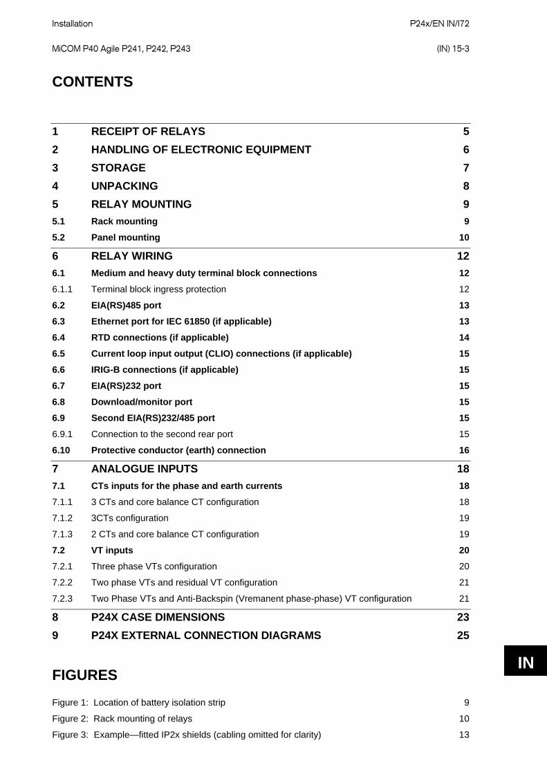
Installation
P24x/EN IN/I72 MiCOM P40 Agile P241, P242, P243 (IN) 15-3
IN
CONTENTS
1 RECEIPT OF RELAYS 5
2 HANDLING OF ELECTRONIC EQUIPMENT 6
3 STORAGE 7
4 UNPACKING 8
5 RELAY MOUNTING 9
5.1 Rack mounting 9
5.2 Panel mounting 10
6 RELAY WIRING 12
6.1 Medium and heavy duty terminal block connections 12
6.1.1 Terminal block ingress protection 12
6.2 EIA(RS)485 port 13
6.3 Ethernet port for IEC 61850 (if applicable) 13
6.4 RTD connections (if applicable) 14
6.5 Current loop input output (CLIO) connections (if applicable) 15
6.6 IRIG-B connections (if applicable) 15
6.7 EIA(RS)232 port 15
6.8 Download/monitor port 15
6.9 Second EIA(RS)232/485 port 15
6.9.1 Connection to the second rear port 15
6.10 Protective conductor (earth) connection 16
7 ANALOGUE INPUTS 18
7.1 CTs inputs for the phase and earth currents 18
7.1.1 3 CTs and core balance CT configuration 18
7.1.2 3CTs configuration 19
7.1.3 2 CTs and core balance CT configuration 19
7.2 VT inputs 20
7.2.1 Three phase VTs configuration 20
7.2.2 Two phase VTs and residual VT configuration 21
7.2.3 Two Phase VTs and Anti-Backspin (Vremanent phase-phase) VT configuration 21
8 P24X CASE DIMENSIONS 23
9 P24X EXTERNAL CONNECTION DIAGRAMS 25
FIGURES Figure 1: Location of battery isolation strip 9
Figure 2: Rack mounting of relays 10
Figure 3: Example—fitted IP2x shields (cabling omitted for clarity) 13
P24x/EN IN/I72
Installation (IN) 15-4 MiCOM P40 Agile P241, P242, P243
IN
Figure 4: 3 CT and core balance CT configuration 18
Figure 5: 3 CT configuration 19
Figure 6: 2 CTs and core balance CT configuration 19
Figure 7: Three phase VTs configuration 20
Figure 8: Two phase VTs and residual VT configuration 21
Figure 9: Two phase VTs and Anti-Backspin (remanent phase-phase) VTconfiguration 22
Figure 10: P241 case dimensions (40TE case) 23
Figure 11: P242 case dimensions (60TE case) 24
Figure 12: P243 case dimensions (80TE case) 24
TABLES Table 1: Blanking plates 10
Table 2: M4 90° crimp ring terminals 12
Table 3: Signals on the Ethernet connector 14
Table 4: Second rear port RS232 connection 16
Table 5: Second rear port RS485 connection 16

Installation
P24x/EN IN/I72 MiCOM P40 Agile P241, P242, P243 (IN) 15-5
IN
1 RECEIPT OF RELAYS Protective relays, although generally of robust construction, require careful treatment prior to installation on site. On receipt, examine the relays immediately to ensure there has been no external damage in transit. If the relay has been damaged, make a claim to the transport contractor and notify Areva promptly.
Relays that are supplied unmounted and not intended for immediate installation should be returned to their protective polythene bags and delivery carton. Section 3 gives more information about the storage of relays.

P24x/EN IN/I72
Installation (IN) 15-6 MiCOM P40 Agile P241, P242, P243
IN
2 HANDLING OF ELECTRONIC EQUIPMENT A person’s normal movements can easily generate electrostatic potentials of several thousand volts. Discharge of these voltages into semiconductor devices when handling electronic circuits can cause serious damage that, although not always immediately apparent, will reduce the reliability of the circuit. This is particularly important to consider where the circuits use complementary metal oxide semiconductors (CMOS), as is the case with these relays.
The relay’s electronic circuits are protected from electrostatic discharge when housed in the case. Do not expose them to risk by removing the front panel or printed circuit boards unnecessarily.
Each printed circuit board incorporates the highest practicable protection for its semiconductor devices. However, if it becomes necessary to remove a printed circuit board, the following precautions should be taken to preserve the high reliability and long life for which the relay has been designed and manufactured.
1. Before removing a printed circuit board, ensure that you are at the same electrostatic potential as the equipment by touching the case.
2. Handle analog input modules by the front panel, frame or edges of the circuit boards. Printed circuit boards should only be handled by their edges. Avoid touching the electronic components, printed circuit tracks or connectors.
3. Do not pass the module to another person without first ensuring you are both at the same electrostatic potential. Shaking hands achieves equipotential.
4. Place the module on an anti-static surface, or on a conducting surface that is at the same potential as yourself.
5. If it is necessary to store or transport printed circuit boards removed from the case, place them individually in electrically conducting anti-static bags.
In the unlikely event that you are making measurements on the internal electronic circuitry of a relay in service, it is preferable that you are earthed to the case with a conductive wrist strap. Wrist straps should have a resistance to ground between 500 kΩ to 10 MΩ. If a wrist strap is not available you should maintain regular contact with the case to prevent a build-up of electrostatic potential. Instrumentation which may be used for making measurements should also be earthed to the case whenever possible.
More information on safe working procedures for all electronic equipment can be found in BS EN 100015: Part 1:1992. It is strongly recommended that detailed investigations on electronic circuitry or modification work should be carried out in a special handling area such as described in the aforementioned British Standard document.
Installation
P24x/EN IN/I72 MiCOM P40 Agile P241, P242, P243 (IN) 15-7
IN
3 STORAGE If the relays are not installed immediately on receipt, store them in a place free from dust and moisture in their original cartons. Keep any de-humidifier bags included in the packing. The de-humidifier crystals lose their efficiency if the bag is exposed to ambient conditions. Restore the crystals by gently heating the bag for about an hour before replacing it in the carton.
To prevent battery drain during transportation and storage a battery isolation strip is fitted during manufacture. With the lower access cover open, presence of the battery isolation strip can be checked by a red tab protruding from the positive side.
On subsequent unpacking, make sure that any dust that has collected on the carton does not fall inside. In locations of high humidity the carton and packing may become impregnated with moisture and the de-humidifier crystals will lose their efficiency.
Prior to installation, relays should be stored at a temperature of between –25º to +70ºC (-13ºF to +158ºF).
P24x/EN IN/I72
Installation (IN) 15-8 MiCOM P40 Agile P241, P242, P243
IN
4 UNPACKING When unpacking and installing the relays, take care not to damage any of the parts and make sure that additional components are not accidentally left in the packing or lost. Do not discard any User’s CDROM or technical documentation - this should accompany the relay to its destination substation.
Note: With the lower access cover open, the red tab of the battery isolation strip will be seen protruding from the positive side of the battery compartment. Do not remove this strip because it prevents battery drain during transportation and storage and will be removed as part of the commissioning tests.
Relays must only be handled by skilled persons.
The site should be well lit to facilitate inspection, clean, dry and reasonably free from dust and excessive vibration. This particularly applies to installations that are being carried out at the same time as construction work.
Installation
P24x/EN IN/I72 MiCOM P40 Agile P241, P242, P243 (IN) 15-9
IN
5 RELAY MOUNTING MiCOM relays are dispatched either individually or as part of a panel/rack assembly.
Individual relays are normally supplied with an outline diagram showing the dimensions for panel cut-outs and hole centers. This information can also be found in the product publication.
Secondary front covers can also be supplied as an option item to prevent unauthorized changing of settings and alarm status. They are available in sizes 40TE (GN0037 001) and 60TE/80TE (GN0038 001) for P24xxxxxxxxxxxA/C and sizes 40TE (GN0242 001) and 60TE/80TE (GN0243 001) for P24xxxxxxxxxxxJ/K.
The relay is designed so the fixing holes in the mounting flanges are only accessible when the access covers are open.
If you include a P991 or MMLG test block with the relays, when viewed from the front position the test block on the right-hand side of the associated relay. This minimizes the wiring between the relay and test block, and allows the correct test block to be easily identified during commissioning and maintenance tests.
P0146ENc
Figure 1: Location of battery isolation strip
If you need to test the relay for the correct operation during the installation, remove the battery isolation strip. If commissioning of the scheme is not imminent, refit the strip to prevent unnecessary battery drain during transportation and installation. The red tab of the isolation strip protrudes from the positive side of the battery compartment when the lower access cover is open. To remove the isolation strip, hold the battery in place and pull the red tab. To refit the battery isolation strip, insert it between the battery compartment positive terminal, with the red tab protruding. See Figure 1.
5.1 Rack mounting MiCOM relays may be rack mounted using single tier rack frames (our part number FX0021 101), as shown in Figure 2. These frames have been designed to have dimensions in accordance with IEC 60297 and are supplied pre-assembled ready to use. On a standard 483 mm rack system this enables combinations of widths of case up to a total equivalent of size 80TE to be mounted side by side.
The two horizontal rails of the rack frame have holes drilled at approximately 26 mm intervals and the relays are attached via their mounting flanges using M4 Taptite self-tapping screws
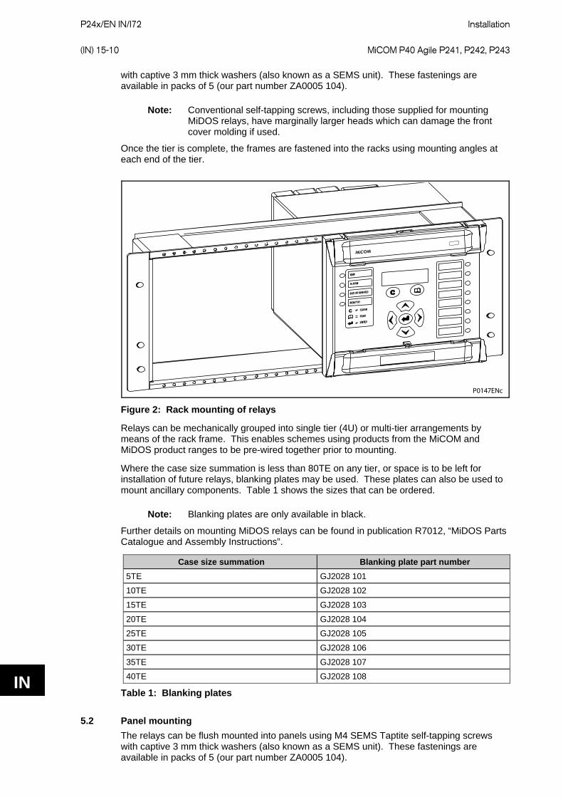
P24x/EN IN/I72
Installation (IN) 15-10 MiCOM P40 Agile P241, P242, P243
IN
with captive 3 mm thick washers (also known as a SEMS unit). These fastenings are available in packs of 5 (our part number ZA0005 104).
Note: Conventional self-tapping screws, including those supplied for mounting MiDOS relays, have marginally larger heads which can damage the front cover molding if used.
Once the tier is complete, the frames are fastened into the racks using mounting angles at each end of the tier.
P0147ENc
Figure 2: Rack mounting of relays
Relays can be mechanically grouped into single tier (4U) or multi-tier arrangements by means of the rack frame. This enables schemes using products from the MiCOM and MiDOS product ranges to be pre-wired together prior to mounting.
Where the case size summation is less than 80TE on any tier, or space is to be left for installation of future relays, blanking plates may be used. These plates can also be used to mount ancillary components. Table 1 shows the sizes that can be ordered.
Note: Blanking plates are only available in black.
Further details on mounting MiDOS relays can be found in publication R7012, “MiDOS Parts Catalogue and Assembly Instructions”.
Case size summation Blanking plate part number 5TE GJ2028 101
10TE GJ2028 102
15TE GJ2028 103
20TE GJ2028 104
25TE GJ2028 105
30TE GJ2028 106
35TE GJ2028 107
40TE GJ2028 108
Table 1: Blanking plates
5.2 Panel mounting The relays can be flush mounted into panels using M4 SEMS Taptite self-tapping screws with captive 3 mm thick washers (also known as a SEMS unit). These fastenings are available in packs of 5 (our part number ZA0005 104).

Installation
P24x/EN IN/I72 MiCOM P40 Agile P241, P242, P243 (IN) 15-11
IN
Note: Conventional self-tapping screws, including those supplied for mounting MiDOS relays, have marginally larger heads which can damage the front cover molding if used.
Alternatively tapped holes can be used if the panel has a minimum thickness of 2.5 mm.
For applications where relays need to be semi-projection or projection mounted, a range of collars are available. Further details can be obtained from the Contracts Department of Areva.
Where several relays are to be mounted in a single cut-out in the panel, it is advised that they are mechanically grouped together horizontally and/or vertically to form rigid assemblies prior to mounting in the panel.
Note: It is not advised that MiCOM relays are fastened using pop rivets as this will not allow the relay to be easily removed from the panel in the future if repair is necessary.
P24x/EN IN/I72
Installation (IN) 15-12 MiCOM P40 Agile P241, P242, P243
IN
6 RELAY WIRING This section serves as a guide to selecting the appropriate cable and connector type for each terminal on the MiCOM relay.
Before carrying out any work on the equipment the user should be familiar with the contents of the Safety Section/Safety Guide Pxxx-SG-4LM-2 or later issue and the ratings on the equipment’s rating label.
6.1 Medium and heavy duty terminal block connections Loose relays are supplied with sufficient M4 screws for making connections to the rear mounted terminal blocks using ring terminals, with a recommended maximum of two ring terminals per relay terminal.
If required, Areva can supply M4 90° crimp ring terminals in three different sizes depending on wire size (see Table 2). Each type is available in bags of 100.
Part number Wire size Insulation color ZB9124 901 0.25 – 1.65 mm2 (22 – 16 AWG) Red
ZB9124 900 1.04 – 2.63 mm2 (16 – 14 AWG) Blue
ZB9124 904 2.53 – 6.64 mm2 (12 – 10 AWG) Uninsulated*
Table 2: M4 90° crimp ring terminals
*To maintain the terminal block insulation requirements for safety, an insulating sleeve should be fitted over the ring terminal after crimping.
The following minimum wire sizes are recommended:
• Current Transformers 2.5 mm2 • Auxiliary Supply, Vx 1.5 mm2 • EIA(RS)485 Port See separate section • Other Circuits 1.0 mm2 Due to the limitations of the ring terminal, the maximum wire size that can be used for any of the medium or heavy duty terminals is 6.0 mm2 using ring terminals that are not pre-insulated. Where it is required to only use pre-insulated ring terminals, the maximum wire size that can be used is reduced to 2.63 mm2 per ring terminal. If a larger wire size is required, two wires should be used in parallel, each terminated in a separate ring terminal at the relay.
The wire used for all connections to the medium and heavy duty terminal blocks, except the first rear EIA(RS)485 port and second rear EIA(RS)232/485 port, should have a minimum voltage rating of 300 Vrms.
It is recommended that the auxiliary supply wiring should be protected by a 16 A high rupture capacity (HRC) fuse of type NIT or TIA. For safety reasons, current transformer circuits must never be fused. Other circuits should be appropriately fused to protect the wire used.
Each opto input has selectable filtering. This allows use of a pre-set filter of ½ cycle which renders the input immune to induced noise on the wiring: although this method is secure it can be slow, particularly for intertripping. This can be improved by switching off the ½ cycle filter in which case one of the following methods to reduce ac noise should be considered. The first method is to use double pole switching on the input, the second is to use screened twisted cable on the input circuit. The recognition time of the opto inputs without the filtering is <2 ms and with the filtering is <12 ms.
6.1.1 Terminal block ingress protection IP2x shields and side cover panels are designed to provide IP20 ingress protection for MiCOM terminal blocks. The shields and covers may be attached during installation or retrofitted to upgrade existing installations—see figure below. More information is available at your local sales office or through our Contact Centre.
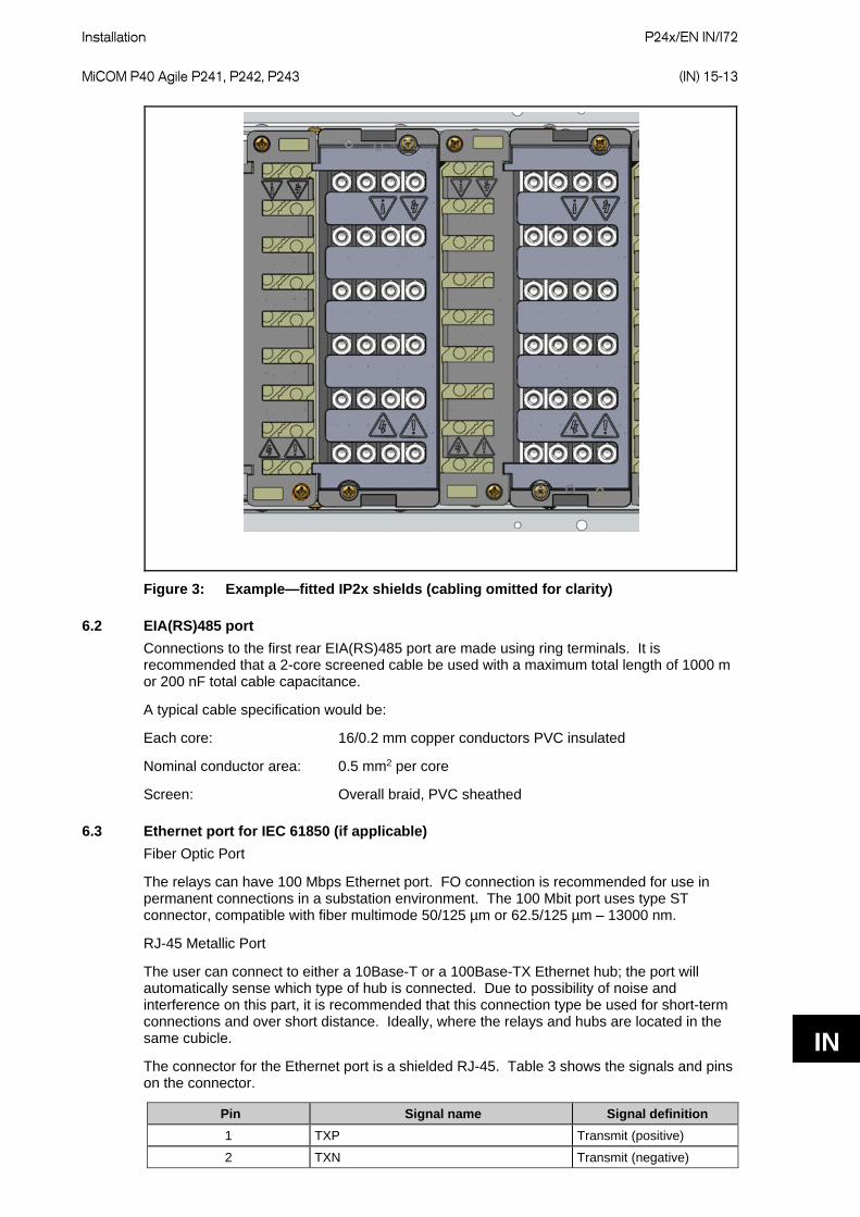
Installation
P24x/EN IN/I72 MiCOM P40 Agile P241, P242, P243 (IN) 15-13
IN
Figure 3: Example—fitted IP2x shields (cabling omitted for clarity)
6.2 EIA(RS)485 port Connections to the first rear EIA(RS)485 port are made using ring terminals. It is recommended that a 2-core screened cable be used with a maximum total length of 1000 m or 200 nF total cable capacitance.
A typical cable specification would be:
Each core: 16/0.2 mm copper conductors PVC insulated
Nominal conductor area: 0.5 mm2 per core
Screen: Overall braid, PVC sheathed
6.3 Ethernet port for IEC 61850 (if applicable) Fiber Optic Port
The relays can have 100 Mbps Ethernet port. FO connection is recommended for use in permanent connections in a substation environment. The 100 Mbit port uses type ST connector, compatible with fiber multimode 50/125 µm or 62.5/125 µm – 13000 nm.
RJ-45 Metallic Port
The user can connect to either a 10Base-T or a 100Base-TX Ethernet hub; the port will automatically sense which type of hub is connected. Due to possibility of noise and interference on this part, it is recommended that this connection type be used for short-term connections and over short distance. Ideally, where the relays and hubs are located in the same cubicle.
The connector for the Ethernet port is a shielded RJ-45. Table 3 shows the signals and pins on the connector.
Pin Signal name Signal definition 1 TXP Transmit (positive)
2 TXN Transmit (negative)
P24x/EN IN/I72
Installation (IN) 15-14 MiCOM P40 Agile P241, P242, P243
IN
Pin Signal name Signal definition 3 RXP Receive (positive)
4 - Not used
5 - Not used
6 RXN Receive (negative)
7 - Not used
8 - Not used
Table 3: Signals on the Ethernet connector
6.4 RTD connections (if applicable) Where RTD inputs are available on a MiCOM relay, the connections are made using screw clamp connectors on the rear of the relay that can accept wire sizes between 0.1 mm2 and 1.5 mm2. The connections between the relay and the RTDs must be made using a screened 3-core cable with a total resistance less than 10 Ω. The cable should have a minimum voltage rating of 300 Vrms.
A 3-core cable should be used even for 2-wire RTD applications, as it allows for the cable’s resistance to be removed from the overall resistance measurement. In such cases the third wire is connected to the second wire at the point the cable is joined to the RTD.
The screen of each cable must only be earthed at one end, preferably at the relay end and must be continuous. Multiple earthing of the screen can cause circulating current to flow along the screen, which induces noise and is unsafe.
It is recommended to minimize noise pick-up in the RTD cables by keeping them close to earthed metal casings and avoiding areas of high electromagnetic and radio interference. The RTD cables should not be run adjacent to or in the same conduit as other high voltage or current cables.
A typical cable specification would be:
Each core: 7/0.2 mm copper conductors heat resistant PVC insulated
Nominal conductor area: 0.22 mm2 per core
Screen: Nickel-plated copper wire braid heat resistant PVC sheathed
The extract below may be useful in defining cable recommendations for the RTDs:
Noise pick up by cables can be categorized in to three types:
• Resistive • Capacitive • Inductive Resistive coupling requires there to be an electrical connection to the noise source. So assuming that the wire and cable insulation is sound and that the junctions are clean then this can be dismissed.
Capacitive coupling requires there to be sufficient capacitance for the impedance path to the noise source to be small enough to allow for significant coupling. This is a function of the dielectric strength between the signal cable on the noise source and the potential (i.e. power) of the noise source.
Inductive coupling occurs when the signal cable is adjacent to a cable/wire carrying the noise or it is exposed to a radiated EMF.
Standard screened cable is normally used to protect against capacitively coupled noise, but in order for it to be effective the screen must only be bonded to the system ground at one point, otherwise a current could flow and the noise would be coupled in to the signal wires of the cable. There are different types of screening available, but basically there are two types: aluminum foil wrap and tin-copper braid.
Foil screens are good for low to medium frequencies and braid is good for high frequencies. High-fidelity screen cables provide both types.
Installation
P24x/EN IN/I72 MiCOM P40 Agile P241, P242, P243 (IN) 15-15
IN
Protection against magnetic inductive coupling requires very careful cable routing and magnetic shielding. The latter can be achieved with steel-armored cable and the use of steel cable trays. It is important the armor of the cable is grounded at both ends so that the EMF of the induced current cancels the field of the noise source and shields the cables conductors from it. (However, the design of the system ground must be considered and care taken to not bridge two isolated ground systems since this could be hazardous and defeat the objectives of the original ground design). The cable should be laid in the cable trays as close as possible to the metal of the tray and under no circumstance should any power cable be in or near to the tray. (Power cables should only cross the signal cables at 90 degrees and never be adjacent to them).
Clearly, both the capacitive and inductive screens must be contiguous from the RTD probes to the relay terminals.
The best types of cable are those provided by the RTD manufactures. These tend to be three conductors (a so call "triad") which are screened with foil. Such triad cables are available in armored forms as well as multi-triad armored forms.
6.5 Current loop input output (CLIO) connections (if applicable) Where current loop inputs and outputs are available on a MiCOM relay, the connections are made using screw clamp connectors, as per the RTD inputs, on the rear of the relay which can accept wire sizes between 0.1 mm2 and 1.5 mm2. It is recommended that connections between the relay and the current loop inputs and outputs are made using a screened cable. The wire should have a minimum voltage rating of 300 Vrms.
6.6 IRIG-B connections (if applicable) The IRIG-B input has a BNC connection. It is recommended that the cable and connector have a characteristic impedance of 50 Ω. It is also recommended that connections between the IRIG-B equipment and the relay are made using coaxial cable 50 Ω characteristic impedance with a halogen free, fire retardant sheath, type RG59LSF.
6.7 EIA(RS)232 port Short term connections to the EIA(RS)232 port, located behind the bottom access cover, can be made using a screened multi-core communication cable up to 15 m long, or a total capacitance of 2500 pF. The cable should be terminated at the relay end with a 9-way, metal shelled, D-type male plug. Section 1.9 of P24x/EN GS of this manual details the pin allocations.
6.8 Download/monitor port Short term connections to the download/monitor port, located behind the bottom access cover, can be made using a screened 25-core communication cable up to 4 m long. The cable should be terminated at the relay end with a 25-way, metal shelled, D-type male plug. Section 1.9 of P24x/EN GS and section 3.5 of P24x/EN CM of this manual details the pin allocations.
6.9 Second EIA(RS)232/485 port Relays with Courier, MODBUS, IEC 60870-5-103 or DNP3 protocol on the first rear communications port have the option of a second rear port, running Courier language. The second rear communications port can be used over one of three physical links: twisted pair K-Bus (non-polarity sensitive), twisted pair EIA(RS)485 (connection polarity sensitive) or EIA(RS)2321.
6.9.1 Connection to the second rear port The second rear Courier port connects via a 9-way female D-type connector (SK4) in the middle of the card end plate (in between IRIG-B connector and lower D-type). The connection is compliant to EIA(RS)574.
For IEC 60870-5-2 over EIA(RS)232/574
1 This port is actually compliant to EIA(RS)574; the 9-pin version of EIA(RS)232, see www.tiaonline.org.
P24x/EN IN/I72
Installation (IN) 15-16 MiCOM P40 Agile P241, P242, P243
IN
Pin Connection 1 No Connection
2 RxD
3 TxD
4 DTR#
5 Ground
6 No Connection
7 RTS#
8 CTS#
9 No Connection
Table 4: Second rear port RS232 connection
Connections to the second rear port configured for EIA(RS)232 operation can be made using a screened multi-core communication cable up to 15 m long, or a total capacitance of 2500 pF. The cable should be terminated at the relay end with a 9-way, metal shelled, D-type male plug. The table above details the pin allocations.
For K-bus or IEC 60870-5-2 over EIA(RS)485
Pin* Connection 4 EIA(RS)485 - 1 (+ ve)
7 EIA(RS)485 - 2 (- ve)
Table 5: Second rear port RS485 connection
* - All other pins unconnected.
# - These pins are control lines for use with a modem.
Note 1: Connector pins 4 and 7 are used by both the EIA(RS)232/574 and EIA(RS)485 physical layers, but for different purposes. Therefore, the cables should be removed during configuration switches.
Note 2: For the EIA(RS)485 protocol an EIA(RS)485 to EIA(RS)232/574 converter will be required to connect a modem or PC running MiCOM S1 Studio, to the relay. A CK222 is recommended.
Note 3: EIA(RS)485 is polarity sensitive, with pin 4 positive (+) and pin 7 negative (-).
Note 4: The K-Bus protocol can be connected to a PC via a KITZ101 or 102.
Note 5: It is recommended that a 2-core screened cable be used. To avoid exceeding the second communications port flash clearances it is recommended that the length of cable between the port and the communications equipment should be less than 300 m. This length can be increased to 1000 m or 200nF total cable capacitance if the communications cable is not laid in close proximity to high current carrying conductors. The cable screen should be earthed at one end only.
A typical cable specification would be:
Each core: 16/0.2 mm copper conductors PVC insulated
Nominal conductor area: 0.5 mm2 per core
Screen: Overall braid, PVC sheathed
6.10 Protective conductor (earth) connection Every relay must be connected to the local earth bar using the M4 earth studs in the bottom left hand corner of the relay case. The minimum recommended wire size is 2.5 mm2 and should have a ring terminal at the relay end. Due to the limitations of the ring terminal, the

Installation
P24x/EN IN/I72 MiCOM P40 Agile P241, P242, P243 (IN) 15-17
IN
maximum wire size that can be used for any of the medium or heavy duty terminals is 6.0 mm2 per wire. If a greater cross-sectional area is required, two parallel connected wires, each terminated in a separate ring terminal at the relay, or a metal earth bar could be used.
Note: To prevent any possibility of electrolytic action between brass or copper earth conductors and the rear panel of the relay, precautions should be taken to isolate them from one another. This could be achieved in a number of ways, including placing a nickel-plated or insulating washer between the conductor and the relay case, or using tinned ring terminals.
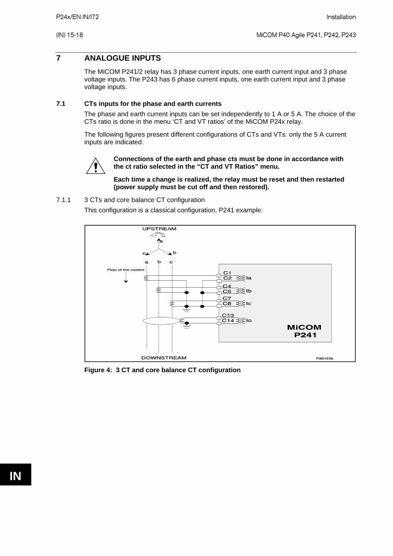
P24x/EN IN/I72
Installation (IN) 15-18 MiCOM P40 Agile P241, P242, P243
IN
7 ANALOGUE INPUTS The MiCOM P241/2 relay has 3 phase current inputs, one earth current input and 3 phase voltage inputs. The P243 has 6 phase current inputs, one earth current input and 3 phase voltage inputs.
7.1 CTs inputs for the phase and earth currents The phase and earth current inputs can be set independently to 1 A or 5 A. The choice of the CTs ratio is done in the menu ‘CT and VT ratios’ of the MiCOM P24x relay.
The following figures present different configurations of CTs and VTs: only the 5 A current inputs are indicated.
Connections of the earth and phase cts must be done in accordance with the ct ratio selected in the “CT and VT Ratios” menu.
Each time a change is realized, the relay must be reset and then restarted (power supply must be cut off and then restored).
7.1.1 3 CTs and core balance CT configuration This configuration is a classical configuration, P241 example:
Figure 4: 3 CT and core balance CT configuration
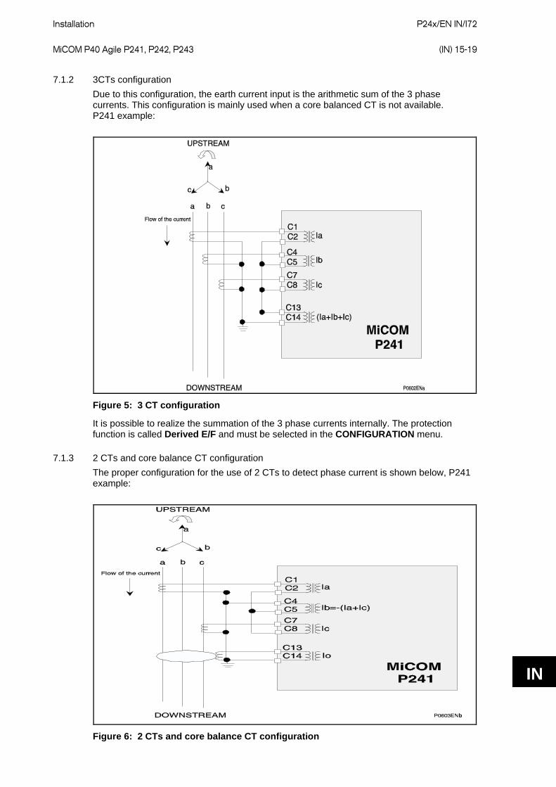
Installation
P24x/EN IN/I72 MiCOM P40 Agile P241, P242, P243 (IN) 15-19
IN
7.1.2 3CTs configuration Due to this configuration, the earth current input is the arithmetic sum of the 3 phase currents. This configuration is mainly used when a core balanced CT is not available. P241 example:
Figure 5: 3 CT configuration
It is possible to realize the summation of the 3 phase currents internally. The protection function is called Derived E/F and must be selected in the CONFIGURATION menu.
7.1.3 2 CTs and core balance CT configuration The proper configuration for the use of 2 CTs to detect phase current is shown below, P241 example:
b
Figure 6: 2 CTs and core balance CT configuration
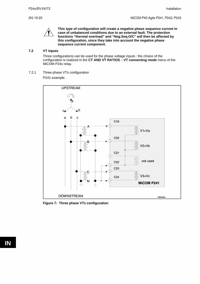
P24x/EN IN/I72
Installation (IN) 15-20 MiCOM P40 Agile P241, P242, P243
IN
This type of configuration will create a negative phase sequence current in case of unbalanced conditions due to an external fault. The protection functions “thermal overload” and “Neg.Seq.O/C” will then be affected by this configuration, since they take into account the negative phase sequence current component.
7.2 VT inputs Three configurations can be used for the phase voltage inputs : the choice of the configuration is realized in the CT AND VT RATIOS – VT connecting mode menu of the MiCOM P24x relay.
7.2.1 Three phase VTs configuration P241 example:
Figure 7: Three phase VTs configuration

Installation
P24x/EN IN/I72 MiCOM P40 Agile P241, P242, P243 (IN) 15-21
IN
7.2.2 Two phase VTs and residual VT configuration P241 example:
P0605ENc
a b c
a
bc
UPSTREAM
A
B
C
C19
C20
C22
C21
C23
C24
V1=Vab
V2=Vcb
not used
V3=V r
MiCOM P241
Residual voltageVr
DOWNSTREAM
Figure 8: Two phase VTs and residual VT configuration
7.2.3 Two Phase VTs and Anti-Backspin (Vremanent phase-phase) VT configuration P241 example:
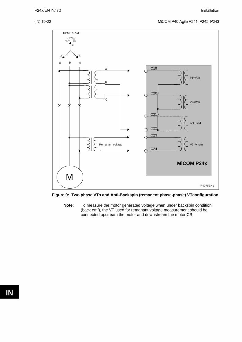
P24x/EN IN/I72
Installation (IN) 15-22 MiCOM P40 Agile P241, P242, P243
IN
P4076ENb
a b c
a
bc
UPSTREAM
A
B
C
C19
C20
C22
C21
C23
C24
V1=Vab
V2=Vcb
not used
V3=V rem
MiCOM P24x
Remanant voltage
XX X
M
Figure 9: Two phase VTs and Anti-Backspin (remanent phase-phase) VTconfiguration
Note: To measure the motor generated voltage when under backspin condition (back emf), the VT used for remanant voltage measurement should be connected upstream the motor and downstream the motor CB.
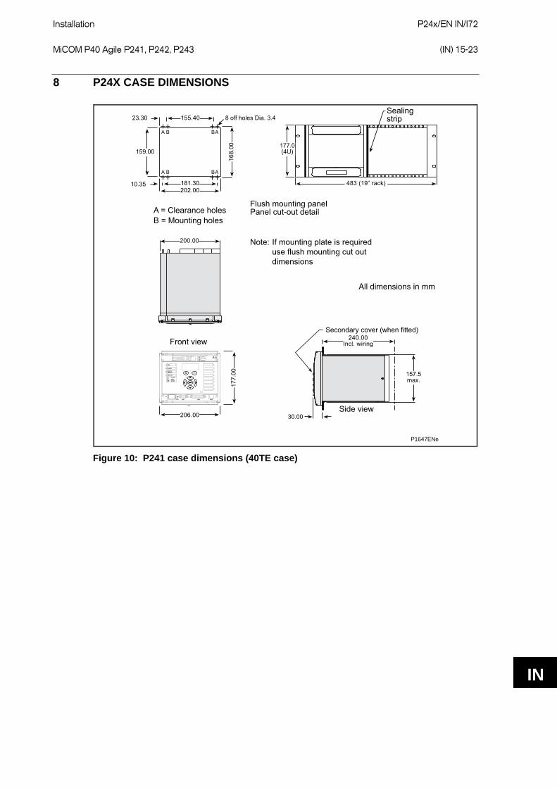
Installation
P24x/EN IN/I72 MiCOM P40 Agile P241, P242, P243 (IN) 15-23
IN
8 P24X CASE DIMENSIONS
P1647ENe
Figure 10: P241 case dimensions (40TE case)
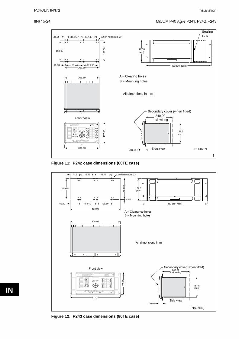
P24x/EN IN/I72
Installation (IN) 15-24 MiCOM P40 Agile P241, P242, P243
IN
A = Clearing holesB = Mounting holes
All dimentions in mm
Front view
Secondary cover (when fitted)
Side view
240.00Incl. wiring
157.5max
30.00309.60
303.50
177.
00
483 (19” rack)
177.0(4U)
Sealingstrip23.25
10.30305.50
129.50155.40
159.00
116.55 142.45 12 off holes Dia. 3.4
168.
00
P1616ENi
f
Figure 11: P242 case dimensions (60TE case)
P1616ENj
Figure 12: P243 case dimensions (80TE case)
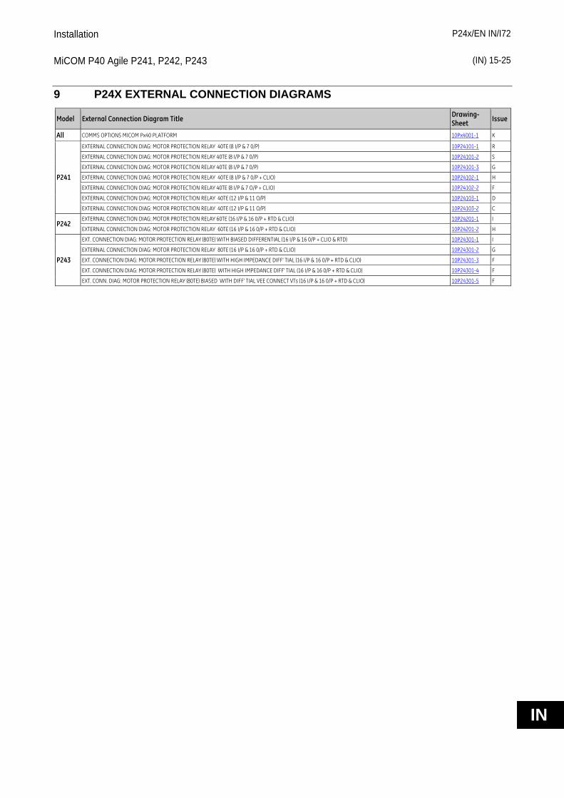
Installation P24x/EN IN/I72
MiCOM P40 Agile P241, P242, P243 (IN) 15-25
IN
9 P24X EXTERNAL CONNECTION DIAGRAMS
Model External Connection Diagram Title Drawing-Sheet Issue
All COMMS OPTIONS MICOM Px40 PLATFORM 10Px4001-1 K
P241
EXTERNAL CONNECTION DIAG: MOTOR PROTECTION RELAY 40TE (8 I/P & 7 0/P) 10P24101-1 R
EXTERNAL CONNECTION DIAG: MOTOR PROTECTION RELAY 40TE (8 I/P & 7 0/P) 10P24101-2 S
EXTERNAL CONNECTION DIAG: MOTOR PROTECTION RELAY 40TE (8 I/P & 7 0/P) 10P24101-3 G
EXTERNAL CONNECTION DIAG: MOTOR PROTECTION RELAY 40TE (8 I/P & 7 0/P + CLIO) 10P24102-1 H
EXTERNAL CONNECTION DIAG: MOTOR PROTECTION RELAY 40TE (8 I/P & 7 O/P + CLIO) 10P24102-2 F
EXTERNAL CONNECTION DIAG: MOTOR PROTECTION RELAY 40TE (12 I/P & 11 O/P) 10P24103-1 D
EXTERNAL CONNECTION DIAG: MOTOR PROTECTION RELAY 40TE (12 I/P & 11 O/P) 10P24103-2 C
P242 EXTERNAL CONNECTION DIAG: MOTOR PROTECTION RELAY 60TE (16 I/P & 16 0/P + RTD & CLIO) 10P24201-1 I
EXTERNAL CONNECTION DIAG: MOTOR PROTECTION RELAY 60TE (16 I/P & 16 0/P + RTD & CLIO) 10P24201-2 H
P243
EXT. CONNECTION DIAG: MOTOR PROTECTION RELAY (80TE) WITH BIASED DIFFERENTIAL (16 I/P & 16 0/P + CLIO & RTD) 10P24301-1 I
EXTERNAL CONNECTION DIAG: MOTOR PROTECTION RELAY 80TE (16 I/P & 16 0/P + RTD & CLIO) 10P24301-2 G
EXT. CONNECTION DIAG: MOTOR PROTECTION RELAY (80TE) WITH HIGH IMPEDANCE DIFF' TIAL (16 I/P & 16 0/P + RTD & CLIO) 10P24301-3 F
EXT. CONNECTION DIAG: MOTOR PROTECTION RELAY (80TE) WITH HIGH IMPEDANCE DIFF' TIAL (16 I/P & 16 0/P + RTD & CLIO) 10P24301-4 F
EXT. CONN. DIAG: MOTOR PROTECTION RELAY (80TE) BIASED WITH DIFF' TIAL VEE CONNECT VTs (16 I/P & 16 0/P + RTD & CLIO) 10P24301-5 F
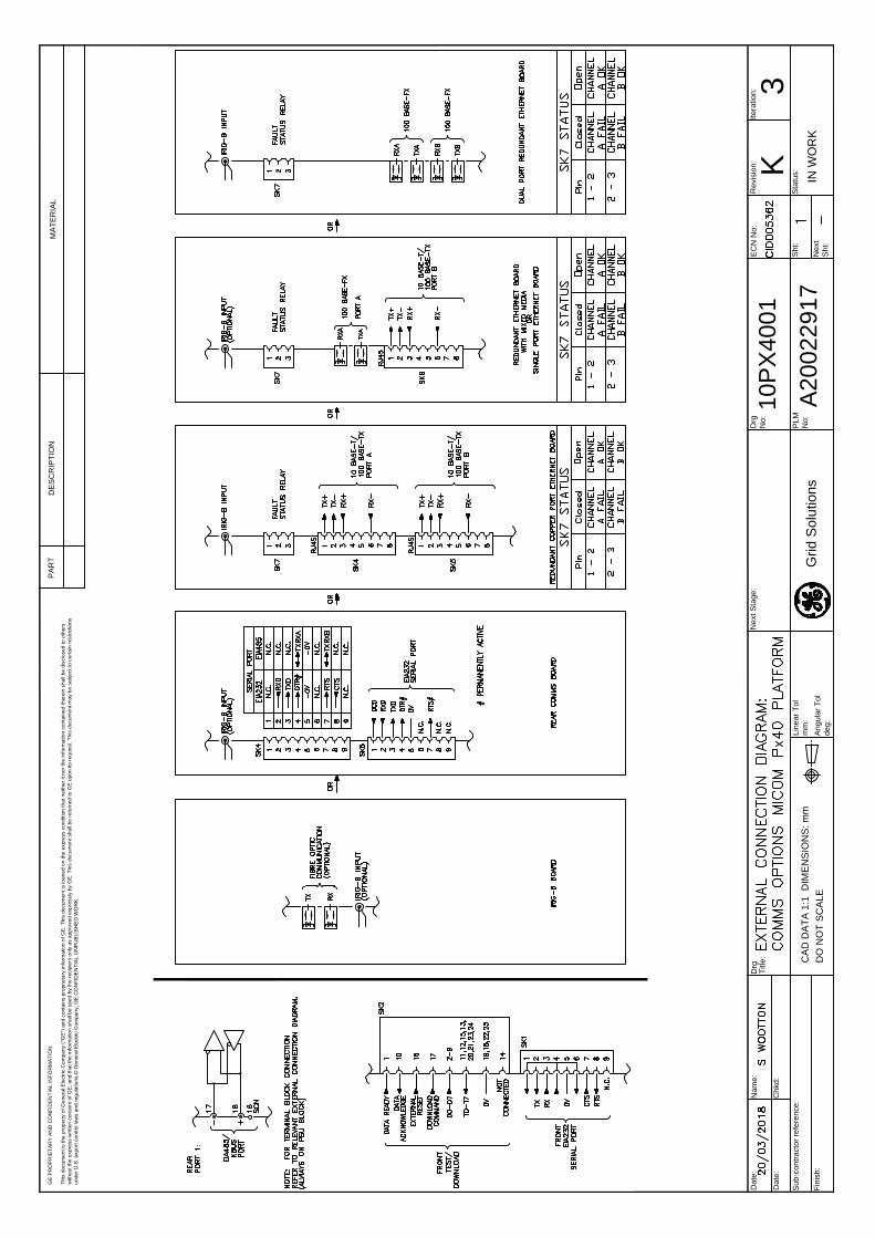
Drg
No
:
Ite
ra
tio
n:
Re
visio
n:
Da
te
:
Da
te
:
Na
me
:
Ch
kd
:
DO
N
OT
S
CA
LE
CA
D D
AT
A 1
:1
D
IM
EN
SIO
NS
: m
m
Title
:
Sh
t:
Ne
xt
Sh
t:
GE
P
RO
PR
IE
TA
RY
A
ND
C
ON
FID
EN
TIA
L IN
FO
RM
AT
IO
N
This docum
ent is the property of G
eneral E
lectric C
om
pany ("G
E") and contains proprietary inform
ation of G
E. T
his docum
ent is loaned on the express condition that neither it nor the inform
ation contained therein shall be disclosed to others
without the express w
ritten consent of G
E, and that the inform
ation shall be used by the recipient only as approved expressly by G
E. T
his docum
ent shall be returned to G
E upon its request. T
his docum
ent m
ay be subject to certain restrictions
under U.S. export control laws and regulations.© General Electric Company, GE CONFIDENTIAL UNPUBLISHED WORK.
PA
RT
DE
SC
RIP
TIO
N
MA
TE
RIA
L
PL
M
No
:
Drg
Ne
xt S
ta
ge
:
Sta
tu
s:
EC
N N
o:
Lin
ea
r T
ol
mm
:
An
gu
la
r T
ol
de
g:
Su
b-co
ntra
cto
r re
fe
re
nce
:
Fin
ish
:
Grid S
olutions
3
IN
W
OR
K
10P
X4001
A20022917
K
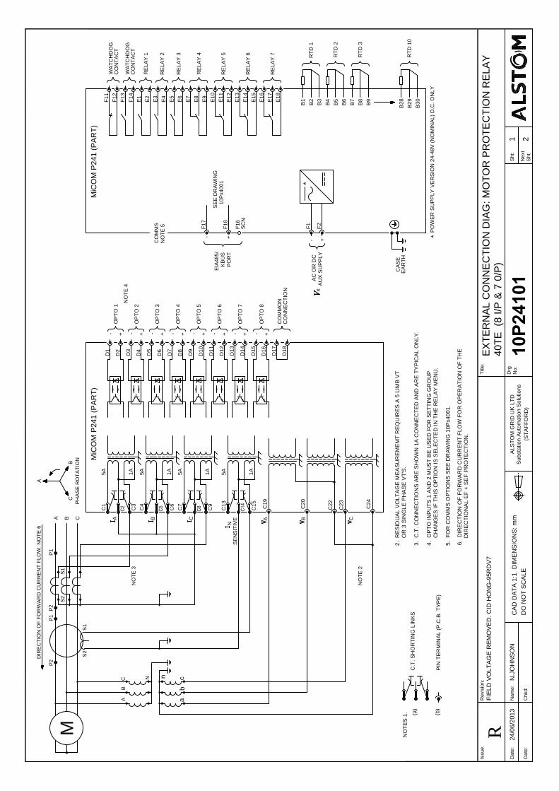
D11
D18
D17
D16
+
-
D15
D14
+
-
D12
D13
+
-
D9
D10
+
-
D8
D7
+
-
+
D6
D5
+
-
D4
D3
-
+
D1
D2
-
CO
NN
EC
TIO
N
CO
MM
ON
OP
TO
8
OP
TO
7
OP
TO
6
OP
TO
5
OP
TO
4
OP
TO
3
OP
TO
2
OP
TO
1
1A
5A
C24
C
C23
BC
20
AC
19
C15
C13
1A
5A
1A
5A
1A
5A
ba
n
c
N
BA
C
C9
C
C7
C6
B
NO
TE
3
C1
C3
C4
A
DIR
EC
TIO
N O
F F
OR
WA
RD
C
UR
RE
NT
F
LO
W. N
OT
E 6
S2
P2
S1
P1
A B CP
HA
SE
R
OT
AT
IO
N
A
CB
M
C22
S2
S1
N
SE
NS
IT
IV
E
P2
P1
NO
TE
2
MiC
OM
P
24
1 (P
AR
T)
NO
TE
4
E7
EA
RT
H
CA
SE
AC
O
R D
C
AU
X S
UP
PLY
x
PO
RT
EIA
485/
KB
US
+
F2
-
F1
*
10P
x4001
SE
E D
RA
WIN
G
F16
SC
N
+
F18
F17
-
RT
D 3
RT
D 10
B30
B29
B28
B9
B8
RT
D 2
RT
D 1
B5
B6
B7
B4
B3
B2
B1
E18
E17
RE
LA
Y 7
E14
E16
E15
E13
E12
RE
LA
Y 6
E11
E10
E8
E9
RE
LA
Y 5
RE
LA
Y 4
CO
MM
S
NO
TE
5
WA
TC
HD
OG
E2
E6
E5
E4
E3
RE
LA
Y 2
E1
F14
F13
F12
WA
TC
HD
OG
CO
NT
AC
T
RE
LA
Y 1
CO
NT
AC
T
F11
RE
LA
Y 3
MiC
OM
P
24
1 (P
AR
T)
C.T
. S
HO
RT
IN
G L
IN
KS
PIN
T
ER
MIN
AL
(P
.C
.B
. T
YP
E)
(a
)
(b
)
NO
TE
S 1
.
OR
3 S
IN
GLE
P
HA
SE
V
T'S
.
5. F
OR
C
OM
MS
O
PT
IO
NS
S
EE
D
RA
WIN
G 10P
x40
01.
CH
AN
GE
S IF
T
HIS
O
PT
IO
N IS
S
ELE
CT
ED
IN
T
HE
R
EL
AY
M
EN
U.
4. O
PT
O IN
PU
TS
1 A
ND
2
M
US
T B
E U
SE
D F
OR
S
ET
TIN
G G
RO
UP
3. C
.T
. C
ON
NE
CT
IO
NS
A
RE
S
HO
WN
1A
C
ON
NE
CT
ED
A
ND
A
RE
T
YP
IC
AL
O
NL
Y.
2. R
ES
ID
UA
L V
OLT
AG
E M
EA
SU
RE
ME
MT
R
EQ
UIR
ES
A
5 LIM
B V
T
6. D
IR
EC
TIO
N O
F F
OR
WA
RD
C
UR
RE
NT
F
LO
W F
OR
O
PE
RA
TIO
N O
F T
HE
DIR
EC
TIO
NA
L E
F +
S
EF
P
RO
TE
CT
IO
N.
PO
WE
R S
UP
PLY
V
ER
SIO
N 24-48V
(N
OM
IN
AL) D
.C
. O
NLY
*
Drg
No
:
Issu
e:
Re
visio
n:
Da
te
:
Da
te
:
Na
me
:
Ch
kd
:
DO
N
OT
S
CA
LE
CA
D D
AT
A 1
:1
D
IM
EN
SIO
NS
: m
m
Title
:
Su
bsta
tio
n A
uto
ma
tio
n S
olu
tio
ns
AL
ST
OM
G
RID
U
K L
TD
(S
TA
FF
OR
D)
Sh
t:
Ne
xt
Sh
t:
24
/0
6/2
01
3N
.JO
HN
SO
N
FIE
LD
V
OL
TA
GE
R
EM
OV
ED
. C
ID
H
ON
G-9
5R
DV
7
10P
24101
1 2
EX
TE
RN
AL C
ON
NE
CT
IO
N D
IA
G: M
OT
OR
P
RO
TE
CT
IO
N R
ELA
Y
40T
E (8 I/P
&
7 0/P
)
R
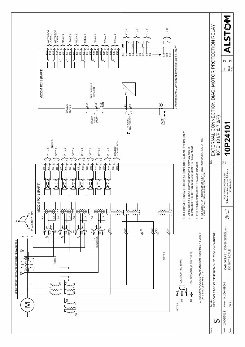
CO
NN
EC
TIO
N
+
D1
7
D1
8
CO
MM
ON
D1
+
D1
5
D1
6
-
D1
3
D1
4
-
OP
TO
8
OP
TO
7
D1
2
D1
1
+
-
D1
0
D9
+
-
OP
TO
6
OP
TO
5
D5
D7
D8
+
-
D6
+
-
OP
TO
4
OP
TO
3
D3
D4
+
-
D2
+
-
OP
TO
2
OP
TO
1
1A
5A
C2
4
NO
TE
2
C2
2
C2
1
C2
0
SE
NS
IT
IV
E
C1
9
C1
5
N
PH
AS
E R
OT
AT
IO
N
A
CB
1A
5A
1A
5A
1A
5A
C6
da
cb
a
dn
C1
3
C
C9
C7
NO
TE
3
N
n
CA
B
B
C4
C3
C1
A
DIR
EC
TIO
N O
F F
OR
WA
RD
C
UR
RE
NT
F
LO
W. N
OT
E 6
M
S2
P2
A
S1
CB
P1
C2
3
NO
TE
4.
MiC
OM
P
24
1 (P
AR
T)
E1
AC
O
R D
C
AU
X S
UP
PL
Y
EA
RT
H
CA
SE
+-
F2
10P
x4001
F1
KB
US
PO
RT
SC
N
+
F16
F18
*
EIA
485/
-
F17
NO
TE
5
CO
MM
S
SE
E D
RA
WIN
G
RT
D 1
B2
B2
9
B2
8
B3
0
RT
D 1
0
B7
B9
B8
B3
B5
B4
B6
RT
D 3
RT
D 2
E1
1
RE
LA
Y 5
RE
LA
Y 6
RE
LA
Y 7
E1
6
B1
E1
8
E1
7
E1
5
E1
4
E1
2
E1
3
RE
LA
Y 1
RE
LA
Y 2
RE
LA
Y 3
RE
LA
Y 4
E6
E1
0
E9
E7
E8
E5
E4
E3
E2
MiC
OM
P
24
1 (P
AR
T)
CO
NT
AC
T
WA
TC
HD
OG
CO
NT
AC
T
WA
TC
HD
OG
F1
4
F1
3
F1
2
F1
1
x
PIN
T
ER
MIN
AL
(P
.C
.B
. T
YP
E)
C.T
. S
HO
RT
IN
G L
IN
KS
(b
)
NO
TE
S 1
.
(a
)
6. D
IR
EC
TIO
N O
F F
OR
WA
RD
C
UR
RE
NT
F
LO
W F
OR
O
PE
RA
TIO
N O
F T
HE
3. C
.T
. C
ON
NE
CT
IO
NS
A
RE
S
HO
WN
1A
C
ON
NE
CT
ED
A
ND
A
RE
T
YP
IC
AL O
NLY
.
4. O
PT
O IN
PU
TS
1 A
ND
2 M
US
T B
E U
SE
D F
OR
S
ET
TIN
G G
RO
UP
CH
AN
GE
S IF
T
HIS
O
PT
IO
N IS
S
ELE
CT
ED
IN
T
HE
R
ELA
Y M
EN
U.
5. F
OR
C
OM
MS
O
PT
IO
NS
S
EE
D
RA
WIN
G 10P
x4001.
DIR
EC
TIO
NA
L E
F +
S
EF
P
RO
TE
CT
IO
N.
2. R
ES
ID
UA
L V
OLT
AG
E M
EA
SU
RE
ME
MT
R
EQ
UIR
ES
A
5 LIM
B V
T
OR
3 S
IN
GLE
P
HA
SE
V
T'S
.
PO
WE
R S
UP
PL
Y V
ER
SIO
N 2
4-4
8V
(N
OM
IN
AL
) D
.C
. O
NL
Y
*
Drg
No
:
Issu
e:
Re
visio
n:
Da
te
:
Da
te
:
Na
me
:
Ch
kd
:
DO
N
OT
S
CA
LE
CA
D D
AT
A 1
:1
D
IM
EN
SIO
NS
: m
m
Title
:
Su
bsta
tio
n A
uto
ma
tio
n S
olu
tio
ns
AL
ST
OM
G
RID
U
K L
TD
(S
TA
FF
OR
D)
Sh
t:
Ne
xt
Sh
t:
24
/0
6/2
01
3N
.JO
HN
SO
N
FIE
LD
V
OL
TA
GE
O
UT
PU
T R
EM
OV
ED
. C
ID
H
ON
G-9
8JC
6A
.
10P
24101
2 3
EX
TE
RN
AL C
ON
NE
CT
IO
N D
IA
G: M
OT
OR
P
RO
TE
CT
IO
N R
ELA
Y
40T
E (8 I/P
&
7 0/P
)
S
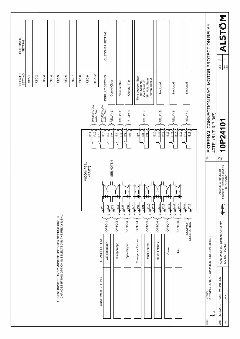
E1
7
E1
8
RE
LA
Y 7
E1
1
E1
4
E1
6
E1
5
E1
3
E1
2
E8
E1
0
E9
E7
E6
RE
LA
Y 5
RE
LA
Y 6
RE
LA
Y 4
E4
E5
E3
E1
E2
F1
4
F1
2
F1
3
F1
1
WA
TC
HD
OG
RE
LA
Y 2
CO
NT
AC
T
RE
LA
Y 1
WA
TC
HD
OG
CO
NT
AC
T
RE
LA
Y 3
DE
FA
ULT
S
ET
TIN
GC
US
TO
ME
R S
ET
TIN
G
Control C
lose
General S
tart
General T
rip
Not U
sed
Not U
sed
Not U
sed
MiC
OM
P
24
1
OP
TO
4
Em
ergency R
estart
D8
D1
7
CO
MM
ON
CO
NN
EC
TIO
N
D1
8
OP
TO
5
OP
TO
6
OP
TO
7
OP
TO
8
+
D1
3
D1
4
D1
5
D1
6
+ +
--
D1
1
D1
2
D1
0
D9
-
+
-
+
Close
Trip
Reset T
herm
al
Reset Latches
(P
AR
T)
OP
TO
1
OP
TO
2
OP
TO
3
D7
D6
D5
D4
-
++
--
D1
D3
D2
+
-
Speed input
CB
open 3ph
DE
FA
ULT
S
ET
TIN
G
CB
closed 3ph
CU
ST
OM
ER
S
ET
TIN
G
Tim
e betw
een S
tart
Hot S
tart N
b.
Cold S
tart N
b.
3P
h V
olt. A
larm
Therm
al lockout
SE
E N
OT
E 4
RT
D 4
RT
D 5
RT
D 6
RT
D 7
RT
D 8
RT
D 9
RT
D 10
SE
TT
IN
G
CU
ST
OM
ER
D
EF
AU
LT
SE
TT
IN
G
RT
D 2
RT
D 3
RT
D 1
CH
AN
GE
S IF
T
HIS
O
PT
IO
N IS
S
ELE
CT
ED
IN
T
HE
R
ELA
Y M
EN
U.
4. O
PT
O IN
PU
TS
1 A
ND
2 M
US
T B
E U
SE
D F
OR
S
ET
TIN
G G
RO
UP
Drg
No
:
Issu
e:
Re
visio
n:
Da
te
:
Da
te
:
Na
me
:
Ch
kd
:
DO
N
OT
S
CA
LE
CA
D D
AT
A 1
:1
D
IM
EN
SIO
NS
: m
m
Title
:
Su
bsta
tio
n A
uto
ma
tio
n S
olu
tio
ns
AL
ST
OM
G
RID
U
K L
TD
(S
TA
FF
OR
D)
Sh
t:
Ne
xt
Sh
t:
25
/1
1/2
01
0W
.L
IN
TE
RN
DR
AW
IN
G O
UT
LIN
E U
PD
AT
ED
. C
ID
B
LIN
-8
BH
LD
T
10P
24101
3
-
EX
TE
RN
AL C
ON
NE
CT
IO
N D
IA
G: M
OT
OR
P
RO
TE
CT
IO
N R
ELA
Y
40T
E (8 I/P
&
7 0/P
)
G

B1
B2
B3
B5
B6
B7
B9
B1
0
B1
1
B1
3
B1
4
B1
6
B1
7
B1
8
B2
0
B2
1
B2
2
B2
4
B2
5
B2
6
B1
5
B2
8
B2
9
B3
0
20
mA
1m
A
1m
A
20
mA
1m
A
20
mA
1m
A
20
mA
1m
A
20
mA
1m
A
20
mA
1m
A
20
mA
20
mA
1m
A
MiC
OM
P
24
1 (P
AR
T)
C2
2
C2
0
C2
3
C2
4
C
NO
TE
2
B
P1
DIR
EC
TIO
N O
F F
OR
WA
RD
C
UR
RE
NT
F
LO
W. N
OT
E 6
n
ca
b
N
M
P2
BA
C
S2
S1
1A
5A
C4
C3
C6
C7
C9
C1
3
C1
5
C1
9A
SE
NS
IT
IV
E
N
NO
TE
3
CB
1A
5A
1A
5A
1A
5A
C1
P1
P2
S2
S1
ACBA
PH
AS
E R
OT
AT
IO
N
A
CB
D1
8
CO
MM
ON
CO
NN
EC
TIO
N
NO
TE
4
D3
D1
6
D1
7
D1
4
D1
5
D1
2
D1
3
D1
1
OP
TO
7
OP
TO
8
+
-
+
OP
TO
6
-
+
-
+
D1
0
D9
D7
D8
D5
D6
D4
+
OP
TO
4
OP
TO
5
+
--
OP
TO
2
OP
TO
3
-
+
-
D2
D1
OP
TO
1
+
-
MiC
OM
P
24
1 (P
AR
T)
F1
4
CO
NT
AC
T
E1
6
E1
8
E1
7
RE
LA
Y 7
E1
5
E1
4
E1
2
E1
3
E1
1
RE
LA
Y 6
RE
LA
Y 5
E8
E1
0
E9
E7
E6
RE
LA
Y 4
E4
E5
E3
E2
E1
RE
LA
Y 2
RE
LA
Y 1
F1
3
F1
2
F1
1
WA
TC
HD
OG
WA
TC
HD
OG
CO
NT
AC
T
10P
x4001
SE
E D
RA
WIN
G
PO
WE
R S
UP
PL
Y V
ER
SIO
N 2
4-4
8V
(N
OM
IN
AL
) D
.C
. O
NL
Y
NO
TE
5
PO
RT
KB
US
EIA
485/
*
SC
N
F16
+
-
F18
F17
CO
MM
S
AC
O
R D
C
AU
X S
UP
PL
Y
EA
RT
H
CA
SE
*
F1
F2
+-
x
RE
LA
Y 3
IN
PU
T 4
IN
PU
T 3
CU
RR
EN
T L
OO
P
IN
PU
TS
&
O
UT
PU
TS
NO
TE
7
CL
IO
IN
PU
T 2
IN
PU
T 1
OU
TP
UT
4
OU
TP
UT
3
OU
TP
UT
2
OU
TP
UT
1
OR
3 S
IN
GLE
P
HA
SE
V
T'S
.
5. F
OR
C
OM
MS
O
PT
IO
NS
S
EE
D
RA
WIN
G 10P
x4001.
DIR
EC
TIO
NA
L E
F +
S
EF
P
RO
TE
CT
IO
N.
CH
AN
GE
S IF
T
HIS
O
PT
IO
N IS
S
ELE
CT
ED
IN
T
HE
R
ELA
Y M
EN
U.
4. O
PT
O IN
PU
TS
1 A
ND
2 M
US
T B
E U
SE
D F
OR
S
ET
TIN
G G
RO
UP
3. C
.T
. C
ON
NE
CT
IO
NS
A
RE
S
HO
WN
1A
C
ON
NE
CT
ED
A
ND
A
RE
T
YP
IC
AL O
NLY
.
2. R
ES
ID
UA
L V
OLT
AG
E M
EA
SU
RE
ME
MT
R
EQ
UIR
ES
A
5 LIM
B V
T
6. D
IR
EC
TIO
N O
F F
OR
WA
RD
C
UR
RE
NT
F
LO
W F
OR
O
PE
RA
TIO
N O
F T
HE
PIN
T
ER
MIN
AL (P
.C
.B
. T
YP
E)
(b)
C.T
. S
HO
RT
IN
G L
IN
KS
NO
TE
S 1.
(a)
FO
R 0-1m
A R
AN
GE
U
SE
1m
A IN
PU
TS
&
O
UT
PU
TS
.
7. F
OR
0-10m
A, 0-20m
A, 4-20m
A R
AN
GE
U
SE
20m
A IN
PU
TS
&
O
UT
PU
TS
Drg
No
:
Issu
e:
Re
visio
n:
Da
te
:
Da
te
:
Na
me
:
Ch
kd
:
DO
N
OT
S
CA
LE
CA
D D
AT
A 1
:1
D
IM
EN
SIO
NS
: m
m
Title
:
Su
bsta
tio
n A
uto
ma
tio
n S
olu
tio
ns
AL
ST
OM
G
RID
U
K L
TD
(S
TA
FF
OR
D)
Sh
t:
Ne
xt
Sh
t:
24
/0
6/2
01
3N
.JO
HN
SO
N
FIE
LD
V
OL
TA
GE
O
UT
PU
T R
EM
OV
ED
. C
ID
H
ON
G-9
8JC
6A
.
10P
24102
1 2
EX
TE
RN
AL C
ON
NE
CT
IO
N D
IA
G: M
OT
OR
P
RO
TE
CT
IO
N R
ELA
Y
40T
E (8 I/P
&
7 0/P
+
C
LIO
)
H
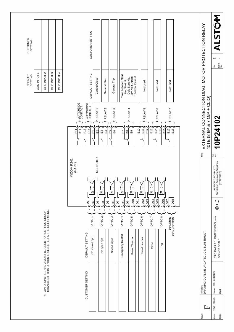
E1
7
E1
8
RE
LA
Y 7
E1
1
E1
4
E1
6
E1
5
E1
3
E1
2
E8
E1
0
E9
E7
E6
RE
LA
Y 5
RE
LA
Y 6
RE
LA
Y 4
E4
E5
E3
E1
E2
F1
4
F1
2
F1
3
F1
1
WA
TC
HD
OG
RE
LA
Y 2
CO
NT
AC
T
RE
LA
Y 1
WA
TC
HD
OG
CO
NT
AC
T
RE
LA
Y 3
DE
FA
ULT
S
ET
TIN
GC
US
TO
ME
R S
ET
TIN
G
Control C
lose
General S
tart
General T
rip
Not U
sed
Not U
sed
Not U
sed
MiC
OM
P
24
1
OP
TO
4
Em
ergency R
estart
D8
D1
7
CO
MM
ON
CO
NN
EC
TIO
N
D1
8
OP
TO
5
OP
TO
6
OP
TO
7
OP
TO
8
+
D1
3
D1
4
D1
5
D1
6
+ +
--
D1
1
D1
2
D1
0
D9
-
+
-
+
Close
Trip
Reset T
herm
al
Reset Latches
(P
AR
T)
OP
TO
1
OP
TO
2
OP
TO
3
D7
D6
D5
D4
-
++
--
D1
D3
D2
+
-
Speed input
CB
open 3ph
DE
FA
ULT
S
ET
TIN
G
CB
closed 3ph
CU
ST
OM
ER
S
ET
TIN
G
Tim
e betw
een S
tart
Hot S
tart N
b.
Cold S
tart N
b.
3P
h V
olt. A
larm
Therm
al lockout
SE
E N
OT
E 4
CH
AN
GE
S IF
T
HIS
O
PT
IO
N IS
S
ELE
CT
ED
IN
T
HE
R
ELA
Y M
EN
U.
4. O
PT
O IN
PU
TS
1 A
ND
2 M
US
T B
E U
SE
D F
OR
S
ET
TIN
G G
RO
UP
C
LIO
IN
PU
T 2
CLIO
IN
PU
T 3
CLIO
IN
PU
T 4
CLIO
IN
PU
T 1
SE
TT
IN
G
DE
FA
ULT
SE
TT
IN
G
CU
ST
OM
ER
Drg
No
:
Issu
e:
Re
visio
n:
Da
te
:
Da
te
:
Na
me
:
Ch
kd
:
DO
N
OT
S
CA
LE
CA
D D
AT
A 1
:1
D
IM
EN
SIO
NS
: m
m
Title
:
Su
bsta
tio
n A
uto
ma
tio
n S
olu
tio
ns
AL
ST
OM
G
RID
U
K L
TD
(S
TA
FF
OR
D)
Sh
t:
Ne
xt
Sh
t:
25
/1
1/2
01
0W
.L
IN
TE
RN
DR
AW
IN
G O
UT
LIN
E U
PD
AT
ED
. C
ID
B
LIN
-8
BH
LD
T
10P
24102
2
-
EX
TE
RN
AL C
ON
NE
CT
IO
N D
IA
G: M
OT
OR
P
RO
TE
CT
IO
N R
ELA
Y
40T
E (8 I/P
&
7 O
/P
+
C
LIO
)
F
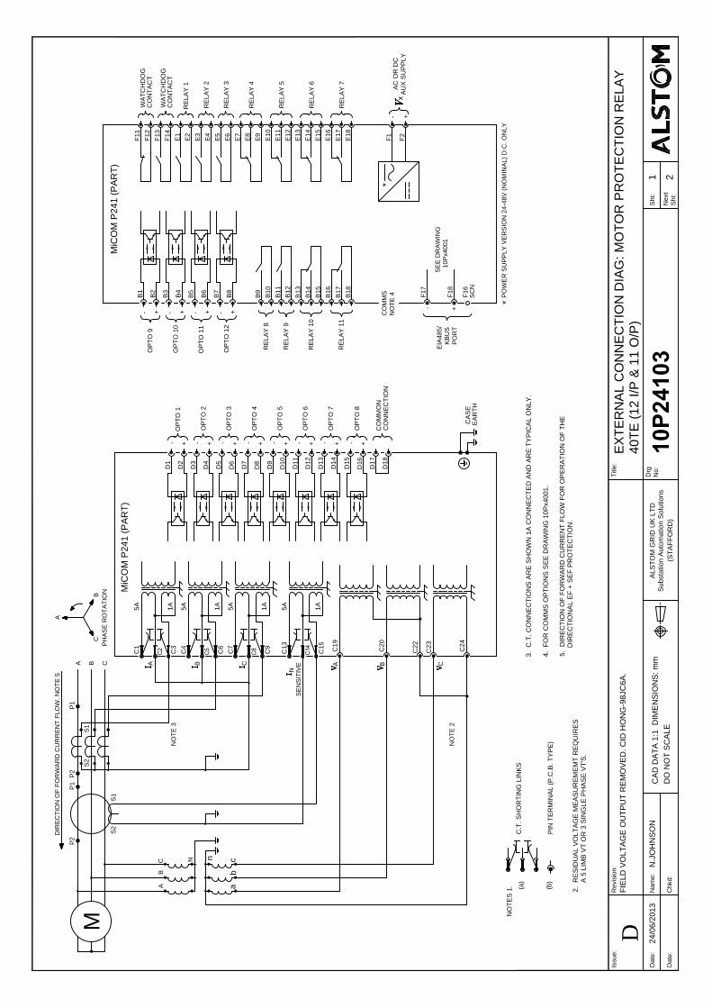
MiC
OM
P
241 (P
AR
T)
C2
2
C2
0
C2
3
C2
4
C
NO
TE
2
B
P1
DIR
EC
TIO
N O
F F
OR
WA
RD
C
UR
RE
NT
F
LO
W. N
OT
E 5
n
ca
b
N
M
P2
BA
C
S2
S1
1A
5A
C4
C3
C6
C7
C9
C1
3
C1
5
C1
9A
SE
NS
IT
IV
E
N
NO
TE
3
CB
1A
5A
1A
5A
1A
5A
C1
P1
P2
S2
S1
ACBA
PH
AS
E R
OT
AT
IO
N
A
CB
D1
8
CO
MM
ON
CO
NN
EC
TIO
N
D3
D1
6
D1
7
D1
4
D1
5
D1
2
D1
3
D1
1
OP
TO
7
OP
TO
8
+
-
+
OP
TO
6
-
+
-
+
D1
0
D9
D7
D8
D5
D6
D4
+
OP
TO
4
OP
TO
5
+
--
OP
TO
2
OP
TO
3
-
+
-
D2
D1
OP
TO
1
+
-
MiC
OM
P
241 (P
AR
T)
F1
4
CO
NT
AC
T
E1
6
E1
8
E1
7
RE
LA
Y 7
E1
5
E1
4
E1
2
E1
3
E1
1
RE
LA
Y 6
RE
LA
Y 5
E8
E1
0
E9
E7
E6
RE
LA
Y 4
E4
E5
E3
E2
E1
RE
LA
Y 2
RE
LA
Y 1
F1
3
F1
2
F1
1
WA
TC
HD
OG
WA
TC
HD
OG
CO
NT
AC
T
10
Px4
00
1
SE
E D
RA
WIN
G
PO
WE
R S
UP
PL
Y V
ER
SIO
N 2
4-4
8V
(N
OM
IN
AL
) D
.C
. O
NL
Y
NO
TE
4
PO
RT
KB
US
EIA
48
5/
*
SC
N
F1
6
+
-
F1
8
F1
7
CO
MM
S
AC
O
R D
C
AU
X S
UP
PL
Y
*
F1
F2
+-
x
RE
LA
Y 3
A 5 LIM
B V
T O
R 3 S
IN
GLE
P
HA
SE
V
T'S
.
4. F
OR
C
OM
MS
O
PT
IO
NS
S
EE
D
RA
WIN
G 10P
x4001.
DIR
EC
TIO
NA
L E
F +
S
EF
P
RO
TE
CT
IO
N.
3. C
.T
. C
ON
NE
CT
IO
NS
A
RE
S
HO
WN
1A
C
ON
NE
CT
ED
A
ND
A
RE
T
YP
IC
AL O
NLY
.
2. R
ES
ID
UA
L V
OLT
AG
E M
EA
SU
RE
ME
MT
R
EQ
UIR
ES
5. D
IR
EC
TIO
N O
F F
OR
WA
RD
C
UR
RE
NT
F
LO
W F
OR
O
PE
RA
TIO
N O
F T
HE
PIN
T
ER
MIN
AL (P
.C
.B
. T
YP
E)
(b)
C.T
. S
HO
RT
IN
G LIN
KS
NO
TE
S 1.
(a)
OP
TO
1
0
OP
TO
9
OP
TO
1
1
OP
TO
1
2
B5
B6
B7
B8
+-+-
B1
B4
B3
B2
+-+-
B1
6
RE
LA
Y 1
1
B1
7
B1
8
RE
LA
Y 1
0
RE
LA
Y 8
RE
LA
Y 9
B1
5
B1
4
B1
2
B1
3
B1
1
B1
0
B9
EA
RT
H
CA
SE
Drg
No
:
Issu
e:
Re
visio
n:
Da
te
:
Da
te
:
Na
me
:
Ch
kd
:
DO
N
OT
S
CA
LE
CA
D D
AT
A 1
:1
D
IM
EN
SIO
NS
: m
m
Title
:
Su
bsta
tio
n A
uto
ma
tio
n S
olu
tio
ns
AL
ST
OM
G
RID
U
K L
TD
(S
TA
FF
OR
D)
Sh
t:
Ne
xt
Sh
t:
24
/0
6/2
01
3N
.JO
HN
SO
N
FIE
LD
V
OL
TA
GE
O
UT
PU
T R
EM
OV
ED
. C
ID
H
ON
G-9
8JC
6A
.
10P
24103
1 2
EX
TE
RN
AL C
ON
NE
CT
IO
N D
IA
G: M
OT
OR
P
RO
TE
CT
IO
N R
ELA
Y
40T
E (12 I/P
&
11 O
/P
)
D
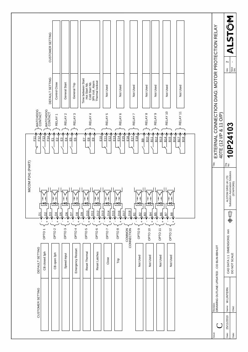
E1
7
E1
8
RE
LA
Y 7
E1
1
E1
4
E1
6
E1
5
E1
3
E1
2
E8
E1
0
E9
E7
E6
RE
LA
Y 5
RE
LA
Y 6
RE
LA
Y 4
E4
E5
E3
E1
E2
F1
4
F1
2
F1
3
F1
1
WA
TC
HD
OG
RE
LA
Y 2
CO
NT
AC
T
RE
LA
Y 1
WA
TC
HD
OG
CO
NT
AC
T
RE
LA
Y 3
DE
FA
ULT
S
ET
TIN
GC
US
TO
ME
R S
ET
TIN
G
Control C
lose
General S
tart
General T
rip
Not U
sed
Not U
sed
Not U
sed
MiC
OM
P
241 (P
AR
T)
OP
TO
4
Em
ergency R
estart
D8
D1
7
CO
MM
ON
CO
NN
EC
TIO
N
D1
8
OP
TO
5
OP
TO
6
OP
TO
7
OP
TO
8
+
D1
3
D1
4
D1
5
D1
6
+ +
--
D1
1
D1
2
D1
0
D9
-
+
-
+
Close
Trip
Reset T
herm
al
Reset Latches
OP
TO
1
OP
TO
2
OP
TO
3
D7
D6
D5
D4
-
++
--
D1
D3
D2
+
-
Speed input
CB
open 3ph
DE
FA
ULT
S
ET
TIN
G
CB
closed 3ph
CU
ST
OM
ER
S
ET
TIN
G
Tim
e betw
een S
tart
Hot S
tart N
b.
Cold S
tart N
b.
3P
h V
olt. A
larm
Therm
al lockout
OP
TO
1
1
Not U
sed
B6
OP
TO
1
2
B8
B7
+
-
+
Not U
sed
OP
TO
9
OP
TO
1
0
B5
B4
B3
B2
-
++
--
B1
Not U
sed
Not U
sed
RE
LA
Y 9
RE
LA
Y 8
RE
LA
Y 1
0
RE
LA
Y 1
1
B1
2
B1
7
B1
8
B1
6
B1
5
B1
4
B1
3
B1
1
B1
0
B9
Not U
sed
Not U
sed
Not U
sed
Not U
sed
Drg
No
:
Issu
e:
Re
visio
n:
Da
te
:
Da
te
:
Na
me
:
Ch
kd
:
DO
N
OT
S
CA
LE
CA
D D
AT
A 1
:1
D
IM
EN
SIO
NS
: m
m
Title
:
Su
bsta
tio
n A
uto
ma
tio
n S
olu
tio
ns
AL
ST
OM
G
RID
U
K L
TD
(S
TA
FF
OR
D)
Sh
t:
Ne
xt
Sh
t:
25
/1
1/2
01
0W
.L
IN
TE
RN
DR
AW
IN
G O
UT
LIN
E U
PD
AT
ED
. C
ID
B
LIN
-8
BH
LD
T
10P
24103
2
-
EX
TE
RN
AL C
ON
NE
CT
IO
N D
IA
G: M
OT
OR
P
RO
TE
CT
IO
N R
ELA
Y
40T
E (12 I/P
&
11 O
/P
)
C
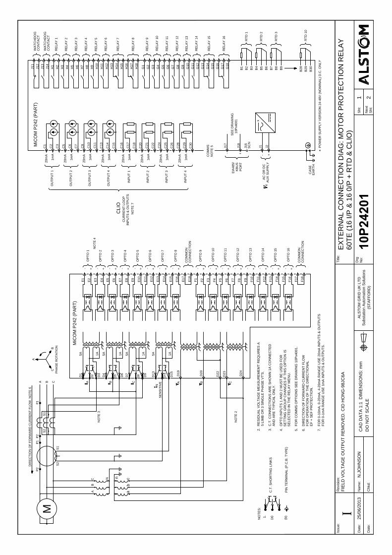
RE
LA
Y 12
G8
B9
B30
B29
B28
RT
D 10
RE
LA
Y 16
RE
LA
Y 14
RE
LA
Y 15
RE
LA
Y 13
B6
B8
B7
B5
B4
B1
B2
B3
G15
G16
G18
G17
G14
G10
G9
G13
G12
G11
RT
D 3
RT
D 2
RT
D 1
RE
LA
Y 3
RE
LA
Y 4
RE
LA
Y 6
RE
LA
Y 7
RE
LA
Y 5
RE
LA
Y 8
RE
LA
Y 9
RE
LA
Y 10
RE
LA
Y 11
G4
G5
G3
G7
G6
H17
H18
H16
G2
G1
H10
H11
H12
H14
H15
H13
H6
H5
H8
H9
H7
CO
NT
AC
T
CO
NT
AC
T
RE
LA
Y 2
RE
LA
Y 1
WA
TC
HD
OG
WA
TC
HD
OG
J14
H1
H4
H3
H2
J11
J12
J13
PO
WE
R S
UP
PLY
V
ER
SIO
N 24-48V
(N
OM
IN
AL) D
.C
. O
NLY
5 LIM
B O
R 3 S
IN
GL
E P
HA
SE
V
T'S
.
2. R
ES
ID
UA
L V
OLT
AG
E M
EA
SU
RE
ME
MT
R
EQ
UIR
ES
A
*
C29
1m
A
C30
C25
20m
A
C28
1m
A
C26
20m
A
C24
1m
A
C22
C21
C5
20m
A
20m
A
C18
20m
A
C20
1m
A
C17
C15
C16
1m
A
C14
20m
A
C11
C13
1m
A
C10
C9
C7
1m
A
20m
A
C6
C1
C3
1m
A
20m
A
C2
MiC
OM
P
242 (P
AR
T)
CA
SE
EA
RT
H
10P
x4001
SE
E D
RA
WIN
G
SC
N
AU
X S
UP
PLY
AC
O
R D
C
x
+-
J1
J2
EIA
485/
KB
US
PO
RT
+
-
J18
J16
J17
NO
TE
5
CO
MM
S
*
SE
LE
CT
ED
IN
T
HE
R
EL
AY
M
EN
U.
3. C
.T
. C
ON
NE
CT
IO
NS
A
RE
S
HO
WN
1A
C
ON
NE
CT
ED
5. F
OR
C
OM
MS
O
PT
IO
NS
S
EE
D
RA
WIN
G 10P
x400
1.
SE
TT
IN
G G
RO
UP
C
HA
NG
ES
IF
T
HIS
O
PT
IO
N IS
4. O
PT
O IN
PU
TS
1 A
ND
2
M
US
T B
E U
SE
D F
OR
1.
C.T
. S
HO
RT
IN
G L
IN
KS
PIN
T
ER
MIN
AL
(P
.C
.B
. T
YP
E)
(b
)
(a
)
NO
TE
S:
AN
D A
RE
T
YP
IC
AL O
NL
Y.
D20
D22
D23
D24
NO
TE
2
CB
DIR
EC
TIO
N O
F F
OR
WA
RD
C
UR
RE
NT
F
LO
W. N
OT
E 6
BA
C
ab
c
N
n
M
S2
P2
1A
5A
1A
5A
D19
1A
5A
1A
5A
A
SE
NS
IT
IV
E
D15
N
D13
NO
TE
3
C
D9
D7
D6
B
D3
D4
PH
AS
E R
OT
AT
IO
N
A
CB
A
S1
S1
S2
D1
ACB
P1
P2
P1
MiC
OM
P
242 (P
AR
T)
CO
MM
ON
CO
NN
EC
TIO
N
F18
OP
TO
1
OP
TO
2
OP
TO
3
OP
TO
4
OP
TO
5
OP
TO
6
OP
TO
7
CO
MM
ON
CO
NN
EC
TIO
N
OP
TO
8
OP
TO
10
OP
TO
11
OP
TO
12
OP
TO
13
OP
TO
14
OP
TO
15
OP
TO
16
OP
TO
9
F9
F17
F16
F15
F14
+
-
+
-
F13
F12
F10
F11
+
-
+
-
F7
F8
F6
F5
+
-
+
-
F4
F3
F2
F1
+ +
--
E10
E15
E16
E17
E18
+
-
+
E11
E12
E13
E14
-
+
-
+
E8
E9
E7
E6
-
+
-
+
E5
E4
E3
E2
-
++
--
NO
TE
4
E1
6. D
IR
EC
TIO
N O
F F
OR
WA
RD
C
UR
RE
NT
F
LO
W
FO
R O
PE
RA
TIO
N O
F T
HE
D
IR
EC
TIO
NA
L
EF
+
S
EF
P
RO
TE
CT
IO
N.
FO
R 0
-1m
A R
AN
GE
U
SE
1m
A IN
PU
TS
&
O
UT
PU
TS
.
7. F
OR
0-1
0m
A, 0-2
0m
A, 4-2
0m
A R
AN
GE
U
SE
20m
A IN
PU
TS
&
O
UT
PU
TS
IN
PU
T 4
IN
PU
T 3
CU
RR
EN
T LO
OP
IN
PU
TS
&
O
UT
PU
TS
NO
TE
7
CLIO
IN
PU
T 2
IN
PU
T 1
OU
TP
UT
4
OU
TP
UT
3
OU
TP
UT
2
OU
TP
UT
1
Drg
No
:
Issu
e:
Re
visio
n:
Da
te
:
Da
te
:
Na
me
:
Ch
kd
:
DO
N
OT
S
CA
LE
CA
D D
AT
A 1
:1
D
IM
EN
SIO
NS
: m
m
Title
:
Su
bsta
tio
n A
uto
ma
tio
n S
olu
tio
ns
AL
ST
OM
G
RID
U
K L
TD
(S
TA
FF
OR
D)
Sh
t:
Ne
xt
Sh
t:
25
/0
6/2
01
3N
.JO
HN
SO
N
FIE
LD
V
OL
TA
GE
O
UT
PU
T R
EM
OV
ED
. C
ID
H
ON
G-9
8JC
6A
10P
24201
1 2
EX
TE
RN
AL C
ON
NE
CT
IO
N D
IA
G: M
OT
OR
P
RO
TE
CT
IO
N R
ELA
Y
60T
E (16 I/P
&
16 0/P
+
R
TD
&
C
LIO
)
I
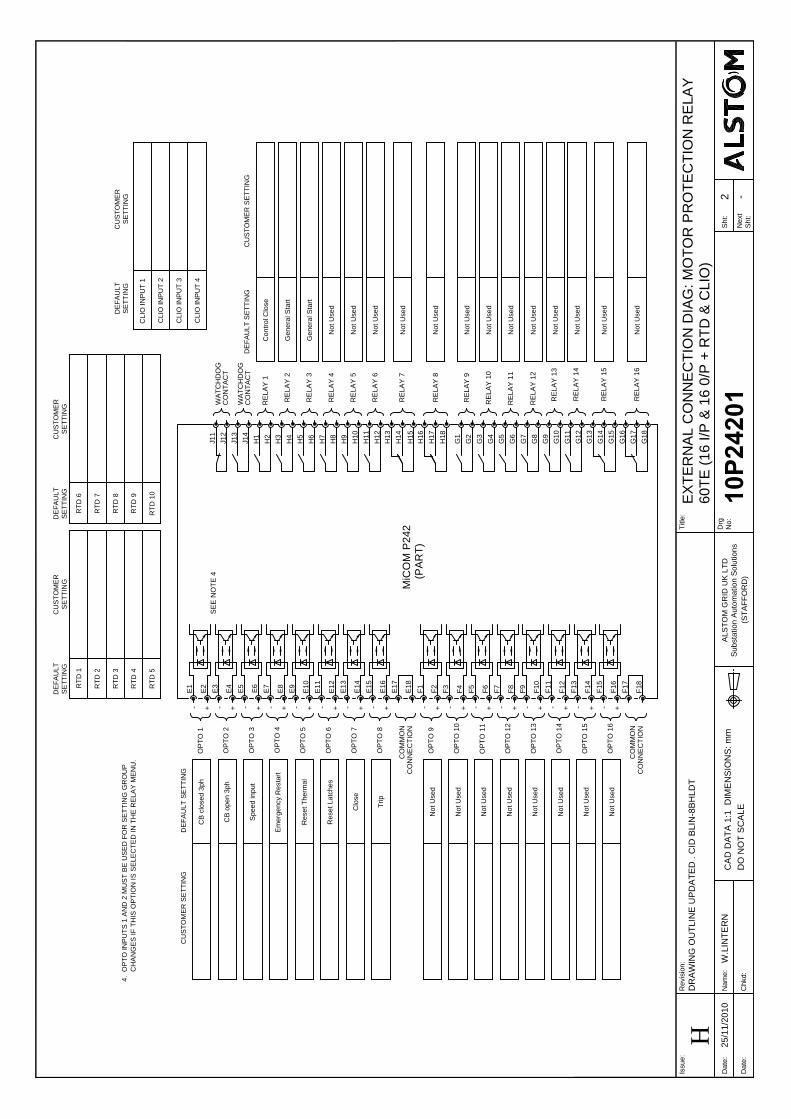
F5
CO
MM
ON
OP
TO
1
6
CO
NN
EC
TIO
N
F1
7
F1
8
F1
6
+
OP
TO
1
1
OP
TO
1
2
OP
TO
1
3
OP
TO
1
4
OP
TO
1
5
F1
3
F1
5
F1
4
F1
2
F1
1
+
--
+
-
+
F9
F1
0
F8
F7
F6
-
++
--
(P
AR
T)
MiC
OM
P
24
2
E1
2
OP
TO
7
OP
TO
8
OP
TO
9
CO
NN
EC
TIO
N
OP
TO
1
0
CO
MM
ON
F4
F3
F1
F2
E1
8
++
--
E1
5
E1
7
E1
6
E1
4
E1
3
+
-
+
-
+
Not U
sed
OP
TO
2
OP
TO
1
OP
TO
3
OP
TO
4
OP
TO
6
OP
TO
5
E7
E1
1
E1
0
E8
E9
-
+
-
+
-
E4
E6
E5
E3
E2
+
-
+
-
+
E1
-
DE
FA
ULT
S
ET
TIN
GC
US
TO
ME
R S
ET
TIN
G
Not U
sed
Not U
sed
Not U
sed
Not U
sed
Not U
sed
Not U
sed
Not U
sed
SE
E N
OT
E 4
CB
closed 3ph
CB
open 3ph
Speed input
Em
ergency R
estart
Reset T
herm
al
Reset Latches
Close
Trip
Not U
sed
RE
LA
Y 1
3
RE
LA
Y 1
4
RE
LA
Y 1
5
RE
LA
Y 1
6
G1
5
G1
7
G1
8
G1
6
G1
2
G1
4
G1
3
G1
0
G1
1
Not U
sed
Not U
sed
Not U
sed
CO
NT
AC
T
WA
TC
HD
OG
RE
LA
Y 1
CO
NT
AC
T
RE
LA
Y 2
RE
LA
Y 3
RE
LA
Y 4
RE
LA
Y 5
RE
LA
Y 6
RE
LA
Y 7
RE
LA
Y 8
RE
LA
Y 9
RE
LA
Y 1
0
WA
TC
HD
OG
RE
LA
Y 1
1
RE
LA
Y 1
2
G7
G9
G8
G6
G5
H1
8
G2
G4
G3
G1
H1
3
H1
5
H1
6
H1
4
H1
7
H1
0
H1
2
H1
1
H9
H8
J1
1
H2
H6
H7
H5
H4
H3
H1
J1
4
J1
2
J1
3
Not U
sed
Not U
sed
Not U
sed
Not U
sed
Not U
sed
DE
FA
ULT
S
ET
TIN
GC
US
TO
ME
R S
ET
TIN
G
Control C
lose
General S
tart
General S
tart
Not U
sed
Not U
sed
Not U
sed
Not U
sed
SE
TT
IN
GS
ET
TIN
GS
ET
TIN
GS
ET
TIN
G
RT
D 4
RT
D 5
RT
D 2
RT
D 3
RT
D 1
RT
D 9
RT
D 10
RT
D 7
RT
D 8
RT
D 6
DE
FA
ULT
C
US
TO
ME
R
DE
FA
ULT
C
US
TO
ME
R
4. O
PT
O IN
PU
TS
1 A
ND
2 M
US
T B
E U
SE
D F
OR
S
ET
TIN
G G
RO
UP
CH
AN
GE
S IF
T
HIS
O
PT
IO
N IS
S
ELE
CT
ED
IN
T
HE
R
ELA
Y M
EN
U.
CLIO
IN
PU
T 2
CLIO
IN
PU
T 3
CLIO
IN
PU
T 4
CLIO
IN
PU
T 1
SE
TT
IN
G
DE
FA
ULT
SE
TT
IN
G
CU
ST
OM
ER
Drg
No
:
Issu
e:
Re
visio
n:
Da
te
:
Da
te
:
Na
me
:
Ch
kd
:
DO
N
OT
S
CA
LE
CA
D D
AT
A 1
:1
D
IM
EN
SIO
NS
: m
m
Title
:
Su
bsta
tio
n A
uto
ma
tio
n S
olu
tio
ns
AL
ST
OM
G
RID
U
K L
TD
(S
TA
FF
OR
D)
Sh
t:
Ne
xt
Sh
t:
25
/1
1/2
01
0W
.L
IN
TE
RN
DR
AW
IN
G O
UT
LIN
E U
PD
AT
ED
. C
ID
B
LIN
-8
BH
LD
T
10P
24201
2
-
EX
TE
RN
AL C
ON
NE
CT
IO
N D
IA
G: M
OT
OR
P
RO
TE
CT
IO
N R
ELA
Y
60T
E (16 I/P
&
16 0/P
+
R
TD
&
C
LIO
)
H
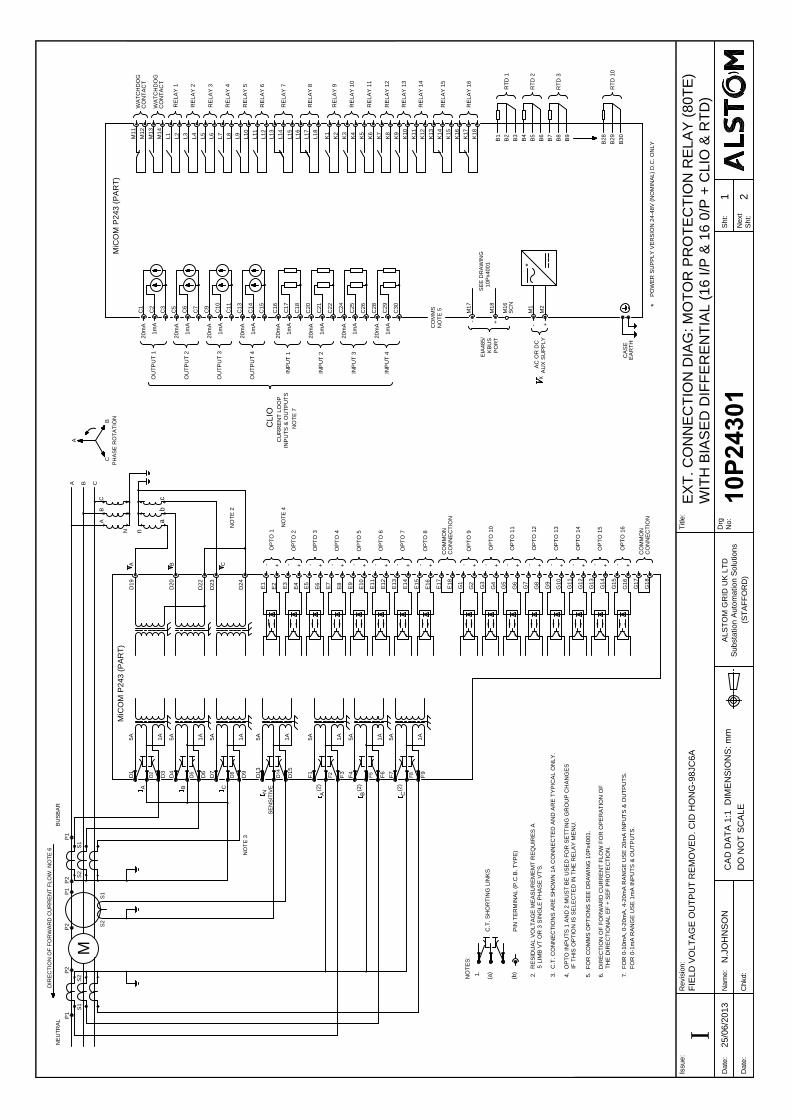
S1
P1
K5
F9
1A
F6
C
F7
B
5A
1A
B7
PO
WE
R S
UP
PLY
V
ER
SIO
N 24-48V
(N
OM
IN
AL) D
.C
. O
NLY
*
B30
B29
B28
B9
B8
EA
RT
H
CA
SE
RT
D 10
RT
D 3
B2
B6
B5
B3
B4
K18
B1
K17
K16
K10
K13
K14
K15
K12
K11
K9
K8
K6
K7
RT
D 1
RT
D 2
RE
LA
Y 16
RE
LA
Y 15
RE
LA
Y 14
RE
LA
Y 12
RE
LA
Y 13
RE
LA
Y 11
D3
F4
F3
A
5A
1A
D15
F1
SE
NS
IT
IV
E
N
D13
5A
1A
5A
NO
TE
3
D9
(2)
C
D7
1A
5A
D6
B
(2)
D4
1A
5A
D24
D23
D22
D20
NO
TE
2
CB
MiC
OM
P
24
3 (P
AR
T)
S1
S2
(2)
A
D1
1A
5A
S2
P2
S2
P2
S1
P1
PH
AS
E R
OT
AT
IO
N
A
CB
B
D19
ac
b
n
A
N
A
C
CB
A
L2
RE
LA
Y 1
L18
K2
K4
K3
K1
L15
L17
L16
L14
L13
L7
L10
L11
L12
L9
L8
L6
L5
L3
L4
RE
LA
Y 10
RE
LA
Y 9
RE
LA
Y 8
RE
LA
Y 7
RE
LA
Y 5
RE
LA
Y 6
RE
LA
Y 4
RE
LA
Y 3
RE
LA
Y 2
M13
L1
M14
M12
M11
MiC
OM
P
243
(P
AR
T)
WA
TC
HD
OG
CO
NT
AC
T
CO
NT
AC
T
WA
TC
HD
OG
M1
7
CO
MM
S
NO
TE
5
M1
8
SC
N
AU
X S
UP
PLY
AC
O
R D
C
x
+-
PO
RT
EIA
48
5/
KB
US
+
-
SE
E D
RA
WIN
G
*
M2
M1
10
Px4
00
1
M1
6
NO
TE
4
E3
G11
OP
TO
14
OP
TO
15
OP
TO
16
CO
NN
EC
TIO
N
-
+
G18
G17
G16
CO
MM
ON
-
+
-
+
G13
G14
G15
G12
OP
TO
10
OP
TO
11
OP
TO
13
OP
TO
12
-
+
-
+
G9
G10
G7
G8
+
-
+
-
+
G5
G6
G4
G3
CO
NN
EC
TIO
N
E16
OP
TO
8
-
+
E18
G1
G2
E17
OP
TO
9
CO
MM
ON
+ +
- -
E15
E14
E12
E13
OP
TO
7
OP
TO
6
- -
+
-
+
E10
E11
E9
E8
OP
TO
5
OP
TO
4
+
-
+
-
E5
E6
E7
E4
OP
TO
3
OP
TO
2
+
-
E1
E2
OP
TO
1
C.T
. S
HO
RT
IN
G LIN
KS
PIN
T
ER
MIN
AL (P
.C
.B
. T
YP
E)
(b)
NO
TE
S:
(a)
1.
3. C
.T
. C
ON
NE
CT
IO
NS
A
RE
S
HO
WN
1A
C
ON
NE
CT
ED
A
ND
A
RE
T
YP
IC
AL O
NLY
.
5. F
OR
C
OM
MS
O
PT
IO
NS
S
EE
D
RA
WIN
G 10P
x4001.
IF
T
HIS
O
PT
IO
N IS
S
ELE
CT
ED
IN
T
HE
R
ELA
Y M
EN
U.
4. O
PT
O IN
PU
TS
1 A
ND
2 M
US
T B
E U
SE
D F
OR
S
ET
TIN
G G
RO
UP
C
HA
NG
ES
5 LIM
B V
T O
R 3 S
IN
GLE
P
HA
SE
V
T'S
.
2. R
ES
ID
UA
L V
OLT
AG
E M
EA
SU
RE
ME
MT
R
EQ
UIR
ES
A
6. D
IR
EC
TIO
N O
F F
OR
WA
RD
C
UR
RE
NT
F
LO
W F
OR
O
PE
RA
TIO
N O
F
TH
E D
IR
EC
TIO
NA
L E
F +
S
EF
P
RO
TE
CT
IO
N.
DIR
EC
TIO
N O
F F
OR
WA
RD
C
UR
RE
NT
F
LO
W. N
OT
E 6
P2
P1
FO
R 0-1m
A R
AN
GE
U
SE
1m
A IN
PU
TS
&
O
UT
PU
TS
.
7. F
OR
0-10m
A, 0-20m
A, 4-20m
A R
AN
GE
U
SE
20m
A IN
PU
TS
&
O
UT
PU
TS
.
M
NE
UT
RA
LB
US
BA
R
IN
PU
TS
&
O
UT
PU
TS
CLIO
NO
TE
7
CU
RR
EN
T LO
OP
20m
A
C30
1m
A
20m
A
1m
A
20m
A
1m
A
IN
PU
T 3
IN
PU
T 4
IN
PU
T 2
C25
C28
C29
C26
C22
C24
C21
20m
A
C11
1m
A
1m
A
20m
A
20m
A
IN
PU
T 1
OU
TP
UT
4
C20
C18
C16
C17
C14
C15
C13
1m
A
20m
A
1m
A
1m
A
20m
A
OU
TP
UT
2
OU
TP
UT
3
OU
TP
UT
1
C6
C9
C10
C7
C3
C5
C2
C1
Drg
No
:
Issu
e:
Re
visio
n:
Da
te
:
Da
te
:
Na
me
:
Ch
kd
:
DO
N
OT
S
CA
LE
CA
D D
AT
A 1
:1
D
IM
EN
SIO
NS
: m
m
Title
:
Su
bsta
tio
n A
uto
ma
tio
n S
olu
tio
ns
AL
ST
OM
G
RID
U
K L
TD
(S
TA
FF
OR
D)
Sh
t:
Ne
xt
Sh
t:
25
/0
6/2
01
3N
.JO
HN
SO
N
FIE
LD
V
OL
TA
GE
O
UT
PU
T R
EM
OV
ED
. C
ID
H
ON
G-9
8JC
6A
10P
24301
1 2
EX
T. C
ON
NE
CT
IO
N D
IA
G: M
OT
OR
P
RO
TE
CT
IO
N R
ELA
Y (80T
E)
WIT
H B
IA
SE
D D
IF
FE
RE
NT
IA
L (16 I/P
&
16 0/P
+
C
LIO
&
R
TD
)
I
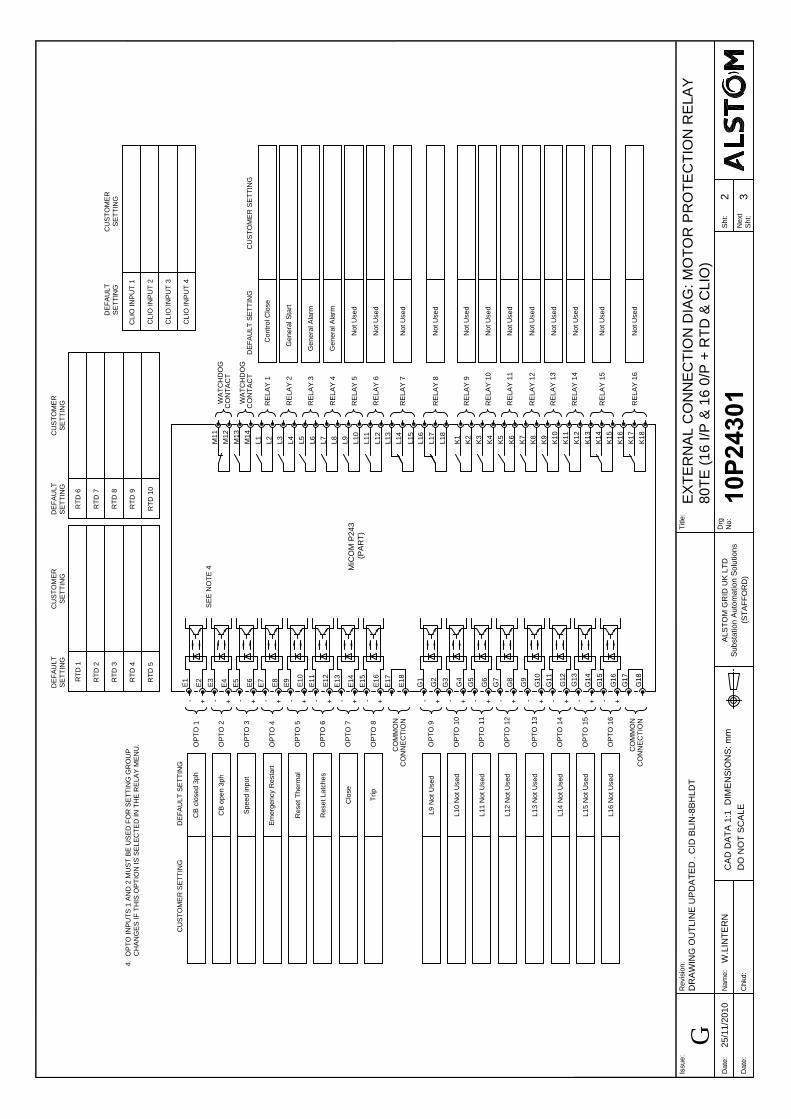
MiC
OM
P
243
OP
TO
4
Em
ergency R
estart
CO
MM
ON
CO
NN
EC
TIO
N
OP
TO
5
OP
TO
6
OP
TO
7
OP
TO
8
+ + +
---
+
-
+
Close
Trip
Reset T
herm
al
Reset Latches
(P
AR
T)
OP
TO
1
OP
TO
2
OP
TO
3
-
++
--
+
-
Speed input
CB
open 3ph
DE
FA
ULT
S
ET
TIN
G
CB
closed 3ph
CU
ST
OM
ER
S
ET
TIN
G
OP
TO
1
1L11 N
ot U
sed
CO
MM
ON
CO
NN
EC
TIO
N
OP
TO
1
6L16 N
ot U
sed
+
-
OP
TO
1
2
OP
TO
1
3
OP
TO
1
4
OP
TO
1
5
L14 N
ot U
sed
L15 N
ot U
sed
L12 N
ot U
sed
L13 N
ot U
sed
+ +
-
+
-
+
--
+
OP
TO
9
OP
TO
1
0
L9 N
ot U
sed
L10 N
ot U
sed
-
+
-
+
-
SE
E N
OT
E 4
E1
1
E1
2
E1
0
E1
3
E1
4
E1
5
E1
6
E1
8
E1
7
E5
E7
E8
E9
E6
E4
E3
E2
E1
G1
0
G1
1
G1
2
G1
3
G1
5
G1
4
G1
7
G1
8
G1
6
G9
G8
G7
G6
G5
G2
G4
G3
G1
K1
6
K1
8
K1
7
RE
LA
Y 1
6
K1
0
K1
3
K1
5
K1
4
K1
1
K1
2
K7
K9
K8
K6
K5
RE
LA
Y 1
5
RE
LA
Y 1
4
RE
LA
Y 1
2
RE
LA
Y 1
3
RE
LA
Y 1
1
WA
TC
HD
OG
L1
1
L1
7
K2
K3
K4
K1
L1
8
L1
4
L1
6
L1
5
L1
2
L1
3
RE
LA
Y 1
0
RE
LA
Y 9
RE
LA
Y 8
RE
LA
Y 7
RE
LA
Y 6
L9
L1
0
L8
L7
L6
L5
L4
L3
L2
L1
M1
4
General A
larm
RE
LA
Y 5
RE
LA
Y 4
RE
LA
Y 3
General S
tart
DE
FA
ULT
S
ET
TIN
G
RE
LA
Y 2
CO
NT
AC
T
RE
LA
Y 1
M1
1
M1
2
M1
3
WA
TC
HD
OG
CO
NT
AC
T
CU
ST
OM
ER
S
ET
TIN
G
Not U
sed
Not U
sed
Not U
sed
Not U
sed
Not U
sed
Not U
sed
Not U
sed
Not U
sed
Not U
sed
Not U
sed
Not U
sed
Not U
sed
General A
larm
Control C
lose
RT
D 5
RT
D 3
RT
D 4
RT
D 1
RT
D 2
DE
FA
ULT
SE
TT
IN
G
CU
ST
OM
ER
SE
TT
IN
G
RT
D 8
RT
D 10
RT
D 9
RT
D 6
DE
FA
ULT
SE
TT
IN
G
RT
D 7
CU
ST
OM
ER
SE
TT
IN
G
4. O
PT
O IN
PU
TS
1 A
ND
2 M
US
T B
E U
SE
D F
OR
S
ET
TIN
G G
RO
UP
CH
AN
GE
S IF
T
HIS
O
PT
IO
N IS
S
ELE
CT
ED
IN
T
HE
R
ELA
Y M
EN
U.
CLIO
IN
PU
T 2
CLIO
IN
PU
T 3
CLIO
IN
PU
T 4
CLIO
IN
PU
T 1
SE
TT
IN
G
DE
FA
ULT
SE
TT
IN
G
CU
ST
OM
ER
Drg
No
:
Issu
e:
Re
visio
n:
Da
te
:
Da
te
:
Na
me
:
Ch
kd
:
DO
N
OT
S
CA
LE
CA
D D
AT
A 1
:1
D
IM
EN
SIO
NS
: m
m
Title
:
Su
bsta
tio
n A
uto
ma
tio
n S
olu
tio
ns
AL
ST
OM
G
RID
U
K L
TD
(S
TA
FF
OR
D)
Sh
t:
Ne
xt
Sh
t:
25
/1
1/2
01
0W
.L
IN
TE
RN
DR
AW
IN
G O
UT
LIN
E U
PD
AT
ED
. C
ID
B
LIN
-8
BH
LD
T
10P
24301
2 3
EX
TE
RN
AL C
ON
NE
CT
IO
N D
IA
G: M
OT
OR
P
RO
TE
CT
IO
N R
ELA
Y
80T
E (16 I/P
&
16 0/P
+
R
TD
&
C
LIO
)
G
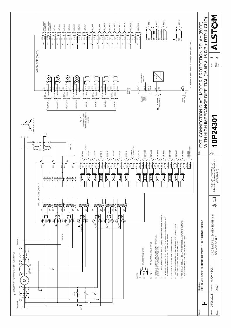
PH
AS
E R
OT
AT
IO
N
A
CB
NO
TE
2
NO
TE
3
S1
P1
S2
S2
M
S2
S1
S1
P2
P2
P2
P1
P1
D2
4
D2
3
C
D2
2
D2
0B
ab
MiC
OM
P
24
3 (P
AR
T)
AD
19
n
N
AB
c
A C
C
B
(2
)
C
F9
(2
)
B
F7
F6
1A
1A
5A
(2
)
A
F3
F4
F1
SE
NS
IT
IV
E
N
D1
5
5A
1A
5A
1A
D7
C
D1
3
D9
B
D6
D4
5A
5A
1A
1A
5A
A
D3
D1
1A
5A
DIR
EC
TIO
N O
F F
OR
WA
RD
C
UR
RE
NT
F
LO
W. N
OT
E 6
NE
UT
RA
LB
US
BA
R
ST
R
NL
R
TH
E D
IR
EC
TIO
NA
L E
F +
S
EF
P
RO
TE
CT
IO
N.
FO
R 0-1m
A R
AN
GE
U
SE
1m
A IN
PU
TS
&
O
UT
PU
TS
.
NO
TE
S:
5. F
OR
C
OM
MS
O
PT
IO
NS
S
EE
D
RA
WIN
G 10P
x4001.
2. R
ES
ID
UA
L V
OLT
AG
E M
EA
SU
RE
ME
MT
R
EQ
UIR
ES
A
(b)
(a)
1.
PIN
T
ER
MIN
AL (P
.C
.B
. T
YP
E)
5 LIM
B V
T O
R 3 S
IN
GLE
P
HA
SE
V
T'S
.
IF
T
HIS
O
PT
IO
N IS
S
ELE
CT
ED
IN
T
HE
R
ELA
Y M
EN
U.
C.T
. S
HO
RT
IN
G LIN
KS
7. F
OR
0-10m
A, 0-20m
A, 4-20m
A R
AN
GE
U
SE
20m
A IN
PU
TS
&
O
UT
PU
TS
.
3. C
.T
. C
ON
NE
CT
IO
NS
A
RE
S
HO
WN
1A
C
ON
NE
CT
ED
A
ND
A
RE
T
YP
IC
AL O
NLY
.
4. O
PT
O IN
PU
TS
1 A
ND
2 M
US
T B
E U
SE
D F
OR
S
ET
TIN
G G
RO
UP
C
HA
NG
ES
6. D
IR
EC
TIO
N O
F F
OR
WA
RD
C
UR
RE
NT
F
LO
W F
OR
O
PE
RA
TIO
N O
F
CO
NN
EC
TIO
N
+
G1
7
G1
8
G1
5
G1
6
-
CO
MM
ON
OP
TO
1
6
OP
TO
1
1
+
G1
0
+ +
G1
4
G1
3
-
G1
2
G1
1
-
OP
TO
1
5
OP
TO
1
4
+ +
G8
G9
-
G6
G7
-
OP
TO
1
2
OP
TO
1
3
CO
NN
EC
TIO
N
-
G1
+ +
-
G4
G5
-
G3
G2
OP
TO
1
0
OP
TO
9
+
E1
7
E1
8
E1
5
E1
6
-
CO
MM
ON
OP
TO
8
OP
TO
3
+
E1
0
+ +
E1
3
E1
4
-
E1
1
E1
2
-
OP
TO
7
OP
TO
6
+ +
E8
E9
-
E6
E7
-
OP
TO
4
OP
TO
5
NO
TE
4
-
E1
+ +
-
E4
E5
-
E2
E3
OP
TO
2
OP
TO
1
PO
WE
R S
UP
PL
Y V
ER
SIO
N 2
4-4
8V
(N
OM
IN
AL
) D
.C
. O
NL
Y
EA
RT
H
CA
SE
*
B3
0
B2
9R
TD
1
0
MiC
OM
P
24
3 (P
AR
T)
C1
0
SC
N
AU
X S
UP
PL
Y
AC
O
R D
C
x
- +
M2
M1
*
KB
US
EIA
48
5/
PO
RT
+
M1
6
M1
8
-
M1
7
10
Px4
00
1
SE
E D
RA
WIN
G
NO
TE
5
CO
MM
S
IN
PU
TS
&
O
UT
PU
TS
CU
RR
EN
T L
OO
P
20
mA
20
mA
20
mA
IN
PU
T 4
IN
PU
T 3
IN
PU
T 2
C2
6
C2
9
1m
A
C3
0
C2
8
C2
4
1m
A
C2
5
1m
A
C2
2
C2
1
20
mA
20
mA
IN
PU
T 1
OU
TP
UT
4
OU
TP
UT
3
C1
5
C1
7
1m
A
C2
0
C1
8
C1
6
C1
3
1m
A
C1
4
1m
A
C1
1
20
mA
20
mA
20
mA
OU
TP
UT
2
OU
TP
UT
1
1m
A
C9
C7
C6
C5
C1
1m
A
C2
C3
K1
1
RT
D 3
B8
B2
8
B9
B5
B7
B6
B3
B4
RT
D 2
B2
B1
K1
7
K1
8
RT
D 1
RE
LA
Y 1
6
K1
4
K1
6
K1
5
K1
2
K1
3
RE
LA
Y 1
5
RE
LA
Y 1
4
L1
8
K5
K8
K9
K1
0
K6
K7
RE
LA
Y 1
2
RE
LA
Y 1
3
RE
LA
Y 1
1
K2
K3
K4
K1
RE
LA
Y 1
0
RE
LA
Y 9
L1
2
RE
LA
Y 6
L1
5
L1
6
L1
7
L1
3
L1
4
RE
LA
Y 8
RE
LA
Y 7
L9
L1
0
L1
1
L8
L7
RE
LA
Y 5
RE
LA
Y 4
L1
L4
L5
L6
L2
L3
RE
LA
Y 2
RE
LA
Y 3
RE
LA
Y 1
M1
2
M1
3
M1
4
M1
1
CO
NT
AC
T
WA
TC
HD
OG
CO
NT
AC
T
WA
TC
HD
OG
NO
TE
7
CL
IO
Drg
No
:
Issu
e:
Re
visio
n:
Da
te
:
Da
te
:
Na
me
:
Ch
kd
:
DO
N
OT
S
CA
LE
CA
D D
AT
A 1
:1
D
IM
EN
SIO
NS
: m
m
Title
:
Su
bsta
tio
n A
uto
ma
tio
n S
olu
tio
ns
AL
ST
OM
G
RID
U
K L
TD
(S
TA
FF
OR
D)
Sh
t:
Ne
xt
Sh
t:
25
/0
6/2
01
3N
.JO
HN
SO
N
FIE
LD
V
OL
TA
GE
O
UT
PU
T R
EM
OV
ED
. C
ID
H
ON
G-9
8JC
6A
10P
24301
3 4
EX
T. C
ON
NE
CT
IO
N D
IA
G: M
OT
OR
P
RO
TE
CT
IO
N R
ELA
Y (80T
E)
WIT
H H
IG
H IM
PE
DA
NC
E D
IF
F' T
IA
L (16 I/P
&
16 0/P
+
R
TD
&
C
LIO
)
F
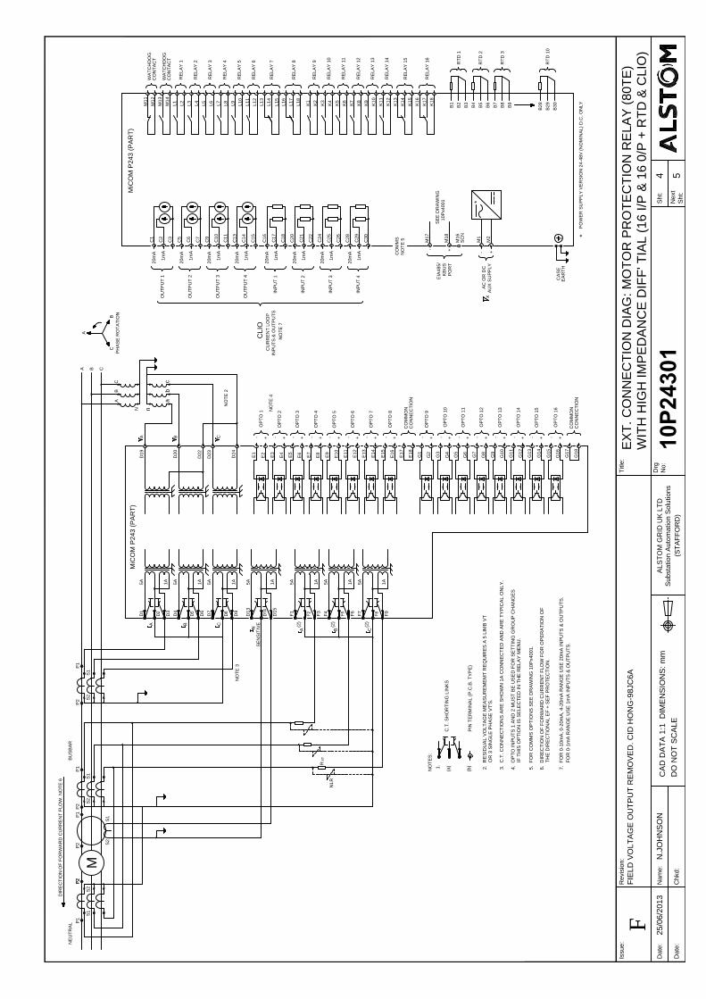
MiC
OM
P
243 (P
AR
T)
(2)
F4
F6
F9
F7
F3
C
(2)
B
(2)
A
1A
1A
5A
5A
1A
NLR
ST
R
M
S1
NE
UT
RA
L
P1
S2
P2
P1
P1
S2
S1
P2
S2
S1
P2
BU
SB
AR
D7
D13
D15
F1
D9
N
SE
NS
IT
IV
E
5A
1A
1A
5A
5A
D1
D3
D4
D6
1A
1A
5A
5A
C
NO
TE
3
B
S2
P2
A
P1
S1
3. C
.T
. C
ON
NE
CT
IO
NS
A
RE
S
HO
WN
1
A C
ON
NE
CT
ED
A
ND
A
RE
T
YP
IC
AL
O
NL
Y.
4. O
PT
O IN
PU
TS
1
A
ND
2
M
US
T B
E U
SE
D F
OR
S
ET
TIN
G G
RO
UP
C
HA
NG
ES
TH
E D
IR
EC
TIO
NA
L E
F +
S
EF
P
RO
TE
CT
IO
N.
FO
R 0
-1
mA
R
AN
GE
U
SE
1
mA
IN
PU
TS
&
O
UT
PU
TS
.
5. F
OR
C
OM
MS
O
PT
IO
NS
S
EE
D
RA
WIN
G 1
0P
x4
00
1.
2. R
ES
ID
UA
L V
OL
TA
GE
M
EA
SU
RE
ME
MT
R
EQ
UIR
ES
A
5
L
IM
B V
T
OR
3
S
IN
GL
E P
HA
SE
V
T'S
.
IF
T
HIS
O
PT
IO
N IS
S
EL
EC
TE
D IN
T
HE
R
EL
AY
M
EN
U.
7. F
OR
0
-1
0m
A, 0
-2
0m
A, 4
-2
0m
A R
AN
GE
U
SE
2
0m
A IN
PU
TS
&
O
UT
PU
TS
.
6. D
IR
EC
TIO
N O
F F
OR
WA
RD
C
UR
RE
NT
F
LO
W F
OR
O
PE
RA
TIO
N O
F
(a
)
(b
)
NO
TE
S:
1.
PIN
T
ER
MIN
AL
(P
.C
.B
. T
YP
E)
C.T
. S
HO
RT
IN
G L
IN
KS
G17
G18
CO
NN
EC
TIO
N
CO
MM
ON
D24
E17
-
+
-
+ + +
--
+
-
+
- - -
++
G8
G12
G16
G15
G14
G13
G10
G11
G9
G3
G6
G7
G5
G4
G1
G2
E18
OP
TO
12
OP
TO
16
OP
TO
15
OP
TO
13
OP
TO
14
OP
TO
11
OP
TO
10
OP
TO
9
CO
NN
EC
TIO
N
CO
MM
ON
-
+
- - -
++ +
-
+
-
+ + +
--
E8
E12
E16
E15
E14
E13
E10
E11
E9
E3
E6
E7
E5
E4
E1
E2
OP
TO
4
OP
TO
8
OP
TO
7
OP
TO
5
OP
TO
6
OP
TO
3
OP
TO
2
NO
TE
4
OP
TO
1
A B C
D23
D22
D20
D19
n
NO
TE
2
ab
c
N
AB
C
CBA
PH
AS
E R
OT
AT
IO
N
A
CB
NO
TE
7
IN
PU
TS
&
O
UT
PU
TS
CU
RR
EN
T LO
OP
CLIO
C13
20m
A
IN
PU
T 1
OU
TP
UT
4
IN
PU
T 2
IN
PU
T 4
IN
PU
T 3
C24
1m
A
C30
20m
A
1m
A
20m
A
C26
C28
C29
C25
1m
A
1m
A
20m
A
C22
C21
C20
C18
20m
A
1m
A
C16
C17
C14
C15
OU
TP
UT
2
OU
TP
UT
1
OU
TP
UT
3
C1
20m
A
1m
A
20m
A
C10
C11
C9
C7
20m
A
1m
A
1m
A
C6
C5
C2
C3
PO
WE
R S
UP
PLY
V
ER
SIO
N 24-48V
(N
OM
IN
AL) D
.C
. O
NLY
*
L9
AC
O
R D
C
AU
X S
UP
PLY
x
K14
NO
TE
5
-
CA
SE
EA
RT
H
+
M2
10P
x4001
SE
E D
RA
WIN
G
KB
US
PO
RT
+
SC
N
M1
M16
M18
EIA
485/
-
M17
*
RT
D 10
B29
B30
B28
B8
B9
B7
B6
RT
D 3
B4
B5
B3
B1
B2
RT
D 2
RT
D 1
K18
K17
K15
K16
RE
LA
Y 16
RE
LA
Y 15
CO
MM
S
K8
RE
LA
Y 12
K11
K12
K13
K10
K9
RE
LA
Y 14
RE
LA
Y 13
K5
K7
K6
K4
K3
RE
LA
Y 11
RE
LA
Y 10
L15
L18
K1
K2
L17
L16
RE
LA
Y 9
RE
LA
Y 8
L12
L14
L13
L11
L10
RE
LA
Y 6
RE
LA
Y 7
RE
LA
Y 5
MiC
OM
P
243 (P
AR
T)
M12
CO
NT
AC
T
L4
RE
LA
Y 2
L8
L7
L5
L6
RE
LA
Y 4
RE
LA
Y 3
L1
L2
L3
M14
M13
RE
LA
Y 1
WA
TC
HD
OG
CO
NT
AC
T
M11
WA
TC
HD
OG
P2
DIR
EC
TIO
N O
F F
OR
WA
RD
C
UR
RE
NT
F
LO
W. N
OT
E 6
Drg
No
:
Issu
e:
Re
visio
n:
Da
te
:
Da
te
:
Na
me
:
Ch
kd
:
DO
N
OT
S
CA
LE
CA
D D
AT
A 1
:1
D
IM
EN
SIO
NS
: m
m
Title
:
Su
bsta
tio
n A
uto
ma
tio
n S
olu
tio
ns
AL
ST
OM
G
RID
U
K L
TD
(S
TA
FF
OR
D)
Sh
t:
Ne
xt
Sh
t:
25
/0
6/2
01
3N
.JO
HN
SO
N
FIE
LD
V
OL
TA
GE
O
UT
PU
T R
EM
OV
ED
. C
ID
H
ON
G-9
8JC
6A
10P
24301
4 5
EX
T. C
ON
NE
CT
IO
N D
IA
G: M
OT
OR
P
RO
TE
CT
IO
N R
ELA
Y (80T
E)
WIT
H H
IG
H IM
PE
DA
NC
E D
IF
F' T
IA
L (16 I/P
&
16 0/P
+
R
TD
&
C
LIO
)
F
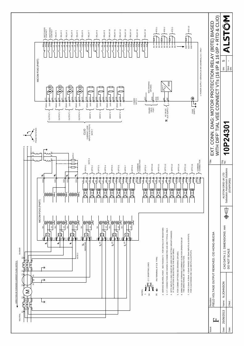
S1
P1
NO
TE
3
D2
4
D2
3
D2
2
D2
0
MiC
OM
P
24
3 (P
AR
T)
S1
S2
S2
P2
S2
P2
S1
P1
PH
AS
E R
OT
AT
IO
N
A
CB
D1
9
P2
P1
NC
B
NO
TE
2
A
ab
c
CB
A
CBA
(2
)
F9
(2
)
B
F7
F6
1A
1A
5A
(2
)
F3
F4
F1
N
D1
5
5A
1A
5A
1A
D7
C
D1
3
D9
B
D6
D4
5A
5A
1A
1A
5A
A
D3
D1
1A
5A
CA
SE
NS
IT
IV
E
DIR
EC
TIO
N O
F F
OR
WA
RD
C
UR
RE
NT
F
LO
W. N
OT
E 6
NE
UT
RA
L
M
BU
SB
AR
K3
B2
8
B2
9
B3
0
PO
WE
R S
UP
PL
Y V
ER
SIO
N 2
4-4
8V
(N
OM
IN
AL
) D
.C
. O
NL
Y
M2
+
AU
X S
UP
PL
Y
CA
SE
EA
RT
H
*
CO
MM
S
NO
TE
5
-
+
PO
RT
AC
O
R D
C
x
-
EIA
48
5/
KB
US
IN
PU
T 3
IN
PU
T 4
1m
A
20
mA
1m
A
M1
M1
6
SC
N
*
SE
E D
RA
WIN
G
10
Px4
00
1
M1
7
M1
8
C3
0
C2
8
C2
9
C2
6
C2
5
RT
D 1
0
B9
B8
B7
RT
D 3
RE
LA
Y 1
5
K1
5
B1
B5
B6
B4
B2
B3
RT
D 2
RT
D 1
RE
LA
Y 1
6
K1
8
K1
6
K1
7
K9
RE
LA
Y 1
3
RE
LA
Y 1
4
K1
2
K1
3
K1
4
K1
1
K1
0
RE
LA
Y 1
0
RE
LA
Y 1
1
RE
LA
Y 1
2
K6
K8
K7
K5
K4
C2
CU
RR
EN
T L
OO
P
IN
PU
TS
&
O
UT
PU
TS
IN
PU
T 2
1m
A
20
mA
20
mA
OU
TP
UT
4
IN
PU
T 1
1m
A
20
mA
1m
A
OU
TP
UT
3
20
mA
20
mA
1m
A
OU
TP
UT
1
OU
TP
UT
2
20
mA
1m
A
1m
A
C1
4
C1
8
C2
4
C2
2
C2
0
C2
1
C1
6
C1
7
C1
5
C1
3
C1
1
C1
0
C9
C5
C6
C7
C3
20
mA
MiC
OM
P
24
3 (P
AR
T)
C1
M1
3
L1
0
L1
6
RE
LA
Y 8
RE
LA
Y 9
K2
K1
L1
8
L1
7
RE
LA
Y 7
RE
LA
Y 6
L1
3
L1
5
L1
4
L1
2
L1
1
RE
LA
Y 3
RE
LA
Y 4
RE
LA
Y 5
L9
L8
L6
L7
L5
CO
NT
AC
T
WA
TC
HD
OG
RE
LA
Y 1
RE
LA
Y 2
L2
L3
L4
M1
4
L1
WA
TC
HD
OG
CO
NT
AC
T
M1
2
M1
1
CL
IO
NO
TE
7
+ +
CO
MM
ON
CO
NN
EC
TIO
N
G1
8
-
G1
3
OP
TO
1
5
OP
TO
1
6
-
G1
5
G1
7
G1
6
+
G1
4
+
OP
TO
1
3
OP
TO
1
4
G1
1
G1
2
+
-
G1
0
G9
+
-
CO
MM
ON
OP
TO
1
0
G4
+
OP
TO
1
2
OP
TO
1
1
+
G8
G7
-
G5
G6
-
OP
TO
9
CO
NN
EC
TIO
N
G2
G3
-
+
G1
E1
8
--
E1
3
OP
TO
7
OP
TO
8
-
E1
5
E1
7
E1
6
+
E1
4
+
OP
TO
5
OP
TO
6
E1
1
E1
2
+
-
E1
0
E9
+
-
OP
TO
2
E4
+
OP
TO
4
OP
TO
3
+
E8
E7
-
E5
E6
-
OP
TO
1
E2
E3
-
+
E1
-
NO
TE
4
2. D
ER
IV
ED
N
EU
TR
AL P
OIN
T. S
EE
P
24X
/E
N T
/- - F
OR
D
ET
AILS
O
F R
ES
IS
TO
RS
6. D
IR
EC
TIO
N O
F F
OR
WA
RD
C
UR
RE
NT
F
LO
W F
OR
O
PE
RA
TIO
N O
F
4. O
PT
O IN
PU
TS
1 A
ND
2 M
US
T B
E U
SE
D F
OR
S
ET
TIN
G G
RO
UP
C
HA
NG
ES
3. C
.T
. C
ON
NE
CT
IO
NS
A
RE
S
HO
WN
1A
C
ON
NE
CT
ED
A
ND
A
RE
T
YP
IC
AL O
NLY
.
7. F
OR
0-10m
A, 0-20m
A, 4-20m
A R
AN
GE
U
SE
20m
A IN
PU
TS
&
O
UT
PU
TS
.
C.T
. S
HO
RT
IN
G LIN
KS
IF
T
HIS
O
PT
IO
N IS
S
ELE
CT
ED
IN
T
HE
R
ELA
Y M
EN
U.
PIN
T
ER
MIN
AL (P
.C
.B
. T
YP
E)
5. F
OR
C
OM
MS
O
PT
IO
NS
S
EE
D
RA
WIN
G 10P
x4001.
FO
R 0-1m
A R
AN
GE
U
SE
1m
A IN
PU
TS
&
O
UT
PU
TS
.
TH
E D
IR
EC
TIO
NA
L E
F +
S
EF
P
RO
TE
CT
IO
N.
NO
TE
S:
(b)
(a)
1.
Drg
No
:
Issu
e:
Re
visio
n:
Da
te
:
Da
te
:
Na
me
:
Ch
kd
:
DO
N
OT
S
CA
LE
CA
D D
AT
A 1
:1
D
IM
EN
SIO
NS
: m
m
Title
:
Su
bsta
tio
n A
uto
ma
tio
n S
olu
tio
ns
AL
ST
OM
G
RID
U
K L
TD
(S
TA
FF
OR
D)
Sh
t:
Ne
xt
Sh
t:
25
/0
6/2
01
3N
.JO
HN
SO
N
FIE
LD
V
OL
TA
GE
O
UT
PU
T R
EM
OV
ED
. C
ID
H
ON
G-9
8JC
6A
10P
24301
5
-
EX
T. C
ON
N. D
IA
G: M
OT
OR
P
RO
TE
CT
IO
N R
ELA
Y (80T
E) B
IA
SE
D
WIT
H D
IF
F' T
IA
L V
EE
C
ON
NE
CT
V
Ts (16 I/P
&
16 0/P
+
R
TD
&
C
LIO
)
F
Firmware and Service Manual Version History
P24x/EN VH/I72
MiCOM P40 Agile P241, P242, P243 (VH) 16-1
VH
FIRMWARE AND SERVICE MANUAL VERSION
HISTORY

P24x/EN VH/I72
Firmware and Service Manual Version History
(VH ) 16-2 MiCOM P40 Agile P241, P242, P243
VH
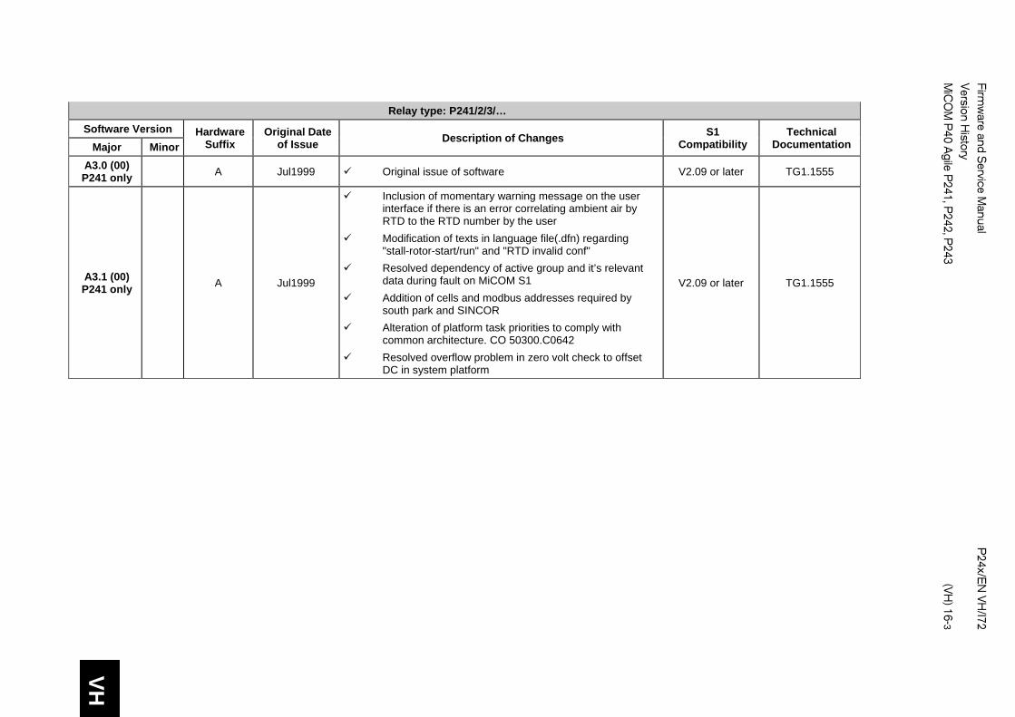
VH
Firmw
are and Service M
anual
P24x/E
N VH
/I72 Version H
istory
M
iCO
M P
40 Agile P
241, P242, P
243
(VH) 16-3
Relay type: P241/2/3/…
Software Version Hardware Suffix
Original Date of Issue Description of Changes S1
Compatibility Technical
Documentation Major Minor A3.0 (00) P241 only A Jul1999 Original issue of software V2.09 or later TG1.1555
A3.1 (00) P241 only A Jul1999
Inclusion of momentary warning message on the user interface if there is an error correlating ambient air by RTD to the RTD number by the user Modification of texts in language file(.dfn) regarding "stall-rotor-start/run" and "RTD invalid conf" Resolved dependency of active group and it’s relevant data during fault on MiCOM S1 Addition of cells and modbus addresses required by south park and SINCOR Alteration of platform task priorities to comply with common architecture. CO 50300.C0642 Resolved overflow problem in zero volt check to offset DC in system platform
V2.09 or later TG1.1555
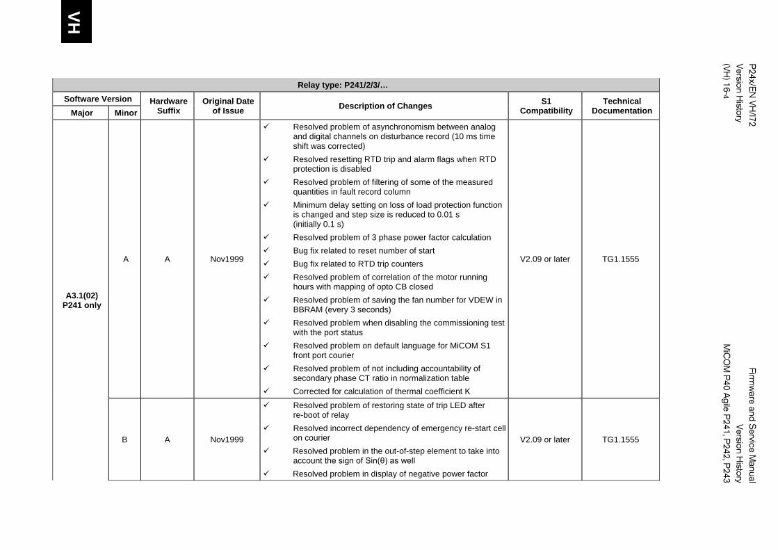
VH
P24x/E
N VH
/I72
Firmw
are and Service M
anual
Version History
Version H
istory (VH
) 16-4
MiC
OM
P40 A
gile P241, P
242, P243
Relay type: P241/2/3/…
Software Version Hardware Suffix
Original Date of Issue Description of Changes S1
Compatibility Technical
Documentation Major Minor
A3.1(02) P241 only
A A Nov1999
Resolved problem of asynchronomism between analog and digital channels on disturbance record (10 ms time shift was corrected) Resolved resetting RTD trip and alarm flags when RTD protection is disabled Resolved problem of filtering of some of the measured quantities in fault record column Minimum delay setting on loss of load protection function is changed and step size is reduced to 0.01 s (initially 0.1 s) Resolved problem of 3 phase power factor calculation Bug fix related to reset number of start Bug fix related to RTD trip counters Resolved problem of correlation of the motor running hours with mapping of opto CB closed Resolved problem of saving the fan number for VDEW in BBRAM (every 3 seconds) Resolved problem when disabling the commissioning test with the port status Resolved problem on default language for MiCOM S1 front port courier Resolved problem of not including accountability of secondary phase CT ratio in normalization table Corrected for calculation of thermal coefficient K
V2.09 or later TG1.1555
B A Nov1999
Resolved problem of restoring state of trip LED after re-boot of relay Resolved incorrect dependency of emergency re-start cell on courier Resolved problem in the out-of-step element to take into
account the sign of Sin(θ) as well Resolved problem in display of negative power factor
V2.09 or later TG1.1555
VH
Firmw
are and Service M
anual
P24x/E
N VH
/I72 Version H
istory
M
iCO
M P
40 Agile P
241, P242, P
243
(VH) 16-5
Relay type: P241/2/3/…
Software Version Hardware Suffix
Original Date of Issue Description of Changes S1
Compatibility Technical
Documentation Major Minor
C A Dec1999 Resolved incorrect dependency of emergency re-start cell on courier Resolved problem of 3 phase reactive power calculation
V2.09 or later TG1.1555
Inclusion of an alarm threshold on energy measurement facility
Inclusion of a second stage in short circuit protection function
Inclusion of derived earth fault protection function Inclusion of a second stage in loss of load/under power
protection function Inclusion of reverse power protection function
VH
P24x/E
N VH
/I72
Firmw
are and Service M
anual
Version History
Version H
istory (VH
) 16-6
MiC
OM
P40 A
gile P241, P
242, P243
Relay type: P241/2/3/…
Software Version Hardware Suffix
Original Date of Issue Description of Changes S1
Compatibility Technical
Documentation Major Minor
A4.0(03) P241 only A Feb2000
Power supply regulator for RTD circuit is changed to 78M05 to establish secure supply
Modification to RTD PCB (01-ZN001001 issue D) Resolved sequencing errors on platform RTD PCB
ZN0010001 for acquisition of measurement at the boundary of 25 degree Celsius
Resolved problem in a modbus method function to cater for data type G10
Resolved problem of restoring trip LED state after re-boot of relay
Resolved initialization problem related to state of LEDs during the first boot of relay
Resolved problem of text inversion in stall protection function
V2.09 or later TG1.1555
A3.1(04) P241 only D A Jul2000
Inclusion of two new cells to describe events: location and index
Modification to modbus address for event recorder Modification of modbus address in "System Data" column Modification of modbus address in "RTD protection"
column Data type G29 ( three 16 bit registers) is replaced with
data type G125 (short float IEEE754 floating point format) to avoid truncation error on measurements
Default text is changed Modbus cell address dedicated to Ubc phase angle
measurement is changed to 30266 Resolved problem of inappropriate measurement
algorithm of reverse 3 phase active and reactive power measurement
V2.09 or later TG1.1555
VH
Firmw
are and Service M
anual
P24x/E
N VH
/I72 Version H
istory
M
iCO
M P
40 Agile P
241, P242, P
243
(VH) 16-7
Relay type: P241/2/3/…
Software Version Hardware Suffix
Original Date of Issue Description of Changes S1
Compatibility Technical
Documentation Major Minor
Two new cells for describing events (location and index) are Added
Modbus addresses are modified in system data column Modbus addresses are modified in RTD protection
column Data type G29 ( three 16 bit registers) is replaced with
data type G125 (short float IEEE754 floating point format) to avoid truncation error on measurements such as KWh
Default text is changed Data types G4, G18 and G26 are modified Modbus cell address dedicated to Ubc phase angle
measurement is changed to 30266 Modbus addressing problem for event file is resolved to
be compliant with other Px40 products Data types G4, G18 and G26 are modified Modbus cell address dedicated to Ubc phase angle
measurement is changed to 30266
VH
P24x/E
N VH
/I72
Firmw
are and Service M
anual
Version History
Version H
istory (VH
) 16-8
MiC
OM
P40 A
gile P241, P
242, P243
Relay type: P241/2/3/…
Software Version Hardware Suffix
Original Date of Issue Description of Changes S1
Compatibility Technical
Documentation Major Minor
A4.0(06) P241 only A A Oct2000
Modbus addressing problem for event file is resolved to be compliant with other Px40 products
Resolved problem of opto reset latches not turning off trip LED to be compliant with other Px40 products
Resolved problem of inappropriate measurement algorithm of reverse 3 phase active and reactive power measurement
Resolved problem of timer initialization on 51LR protection function
Inclusion of the option "reset energies" in " measurement 2" column
Resolved problem of incorrect calculation methodology in measurement of time to next start
Resolved problem of not resetting on software counter used for "emergency re-start"
Resolved problem of counting methodology for the "number of hot(cold) starts"
Resolved problem of visibility on LCD Resolved missing modbus address (operand) of the cell
091D Resolved courier coordinate cell error regarding second
stage overcurrent pickup setting Resolved correlation problem between relay output 3
operation and CB operating time counter Hysterisis for under/over frequency protection function is
reduced to 0.05 Hz
V2.09 or later TG1.1555
A3.1(07) P241 only
Cont.. E A
Inclusion of filters for event recorder RDF file is modified Courier co-ordinates in the communication column are
modified to relieve inconsistency in courier communication cell [0Exx] numbering
V2.09 or later TG1.1555

VH
Firmw
are and Service M
anual
P24x/E
N VH
/I72 Version H
istory
M
iCO
M P
40 Agile P
241, P242, P
243
(VH) 16-9
Relay type: P241/2/3/…
Software Version Hardware Suffix
Original Date of Issue Description of Changes S1
Compatibility Technical
Documentation Major Minor
A4.1 (08) P241 only
B A Dec2000
Resolved problem of inaccuracies in KWh measurement which arises after a long period of operation
The two thresholds of the overcurrent protection function are changed from 1 A to 0.2 A. Also the second threshold of the I2 overcurrent protection function is changed from 0.2 A to 0.05 A
V2.09 or later TG1.1555
C A Feb2001
Resolved problem of timer start initialization for drop off time of the out-of-step protection function
Resolved problem of opto command to change setting group
Resolved problem of cold(hot) number of start after re-boot of relay
Resolved problem of inaccuracies in KWh measurement
V2.09 or later TG1.1555
D A Apr2001
Correction for number of registers declared in the modbus (2 instead of 3 on G125 only) Resolved problem of fault current measurement via modbus with G125 format
V2.09 or later TG1.1555
E A Sep2001
Resolved incorrect generation of error code 0x9300ffd2 which occurred during short circuit test at 70 Hz
Corrected for wrong phase indication at the time of undervoltage protection activity
V2.09 or later TG1.1555
F A Nov2001
Corrected for proper RTD number indication when corresponding RTD trip cell is active
Correction for intermittent twice resetting requirement of trip LED
Resolved initialization problem related to protection/PSL programs secondary effect on LEDs and output relays
V2.09 or later TG1.1555
G A Nov2001 Resolved initialization problem related to protection/PSL programs secondary effect on LEDs and output relays V2.09 or later TG1.1555
H A Nov2001 Resolved incorrect timing for trip operation under second stage negative phase sequence protection function V2.09 or later TG1.1555
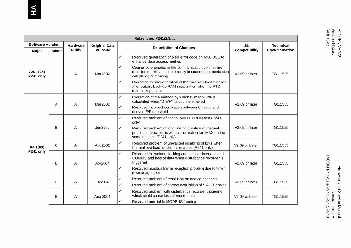
VH
P24x/E
N VH
/I72
Firmw
are and Service M
anual
Version History
Version H
istory (VH
) 16-10
MiC
OM
P40 A
gile P241, P
242, P243
Relay type: P241/2/3/…
Software Version Hardware Suffix
Original Date of Issue Description of Changes S1
Compatibility Technical
Documentation Major Minor
A4.1 (08) P241 only A Mar2002
Resolved generation of plerr error code on MODBUS to enhance data access method
Courier co-ordinates in the communication column are modified to relieve inconsistency in courier communication cell [0Exx] numbering
Corrected for mal-operation of thermal over load function after battery back-up RAM initialization when no RTD module is present
V2.09 or later TG1.1555
A4.1(09) P241 only
A A Mar2002
Correction of the method by which I2 magnitude is calculated when "D E/F" function is enabled
Resolved incorrect correlation between CT ratio and derived E/F threshold
V2.09 or later TG1.1555
B A Jun2002
Resolved problem of continuous EEPROM test (P241 only)
Resolved problem of long polling duration of thermal protection function as well as correction for IMAX on the same function (P241 only)
V2.09 or later TG1.1555
C A Aug2002 Resolved problem of unwanted disabling of I2>1 when thermal overload function is enabled (P241 only) V2.09 or Later TG1.1555
E A Apr2004
Resolved intermittent locking out the user interface and COMMS and loss of data when disturbance recorder is triggered
Resolved modbus frame reception problem due to timer mismanagement
V2.09 or later TG1.1555
F A Dec-04 Resolved problem of resolution on analog channels Resolved problem of correct acquisition of 5 A CT choice
V2.09 or later TG1.1555
E A Aug 2004 Resolved problem with disturbance recorder triggering
which could cause loss of record data Resolved unreliable MODBUS framing
V2.09 or Later TG1.1555
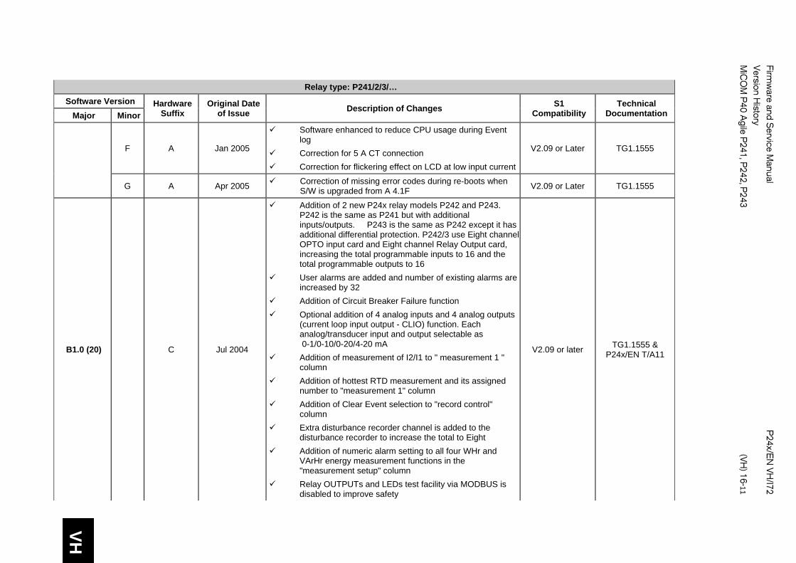
VH
Firmw
are and Service M
anual
P24x/E
N VH
/I72 Version H
istory
M
iCO
M P
40 Agile P
241, P242, P
243
(VH) 16-11
Relay type: P241/2/3/…
Software Version Hardware Suffix
Original Date of Issue Description of Changes S1
Compatibility Technical
Documentation Major Minor
F A Jan 2005
Software enhanced to reduce CPU usage during Event log
Correction for 5 A CT connection Correction for flickering effect on LCD at low input current
V2.09 or Later TG1.1555
G A Apr 2005 Correction of missing error codes during re-boots when S/W is upgraded from A 4.1F V2.09 or Later TG1.1555
B1.0 (20) C Jul 2004
Addition of 2 new P24x relay models P242 and P243. P242 is the same as P241 but with additional inputs/outputs. P243 is the same as P242 except it has additional differential protection. P242/3 use Eight channel OPTO input card and Eight channel Relay Output card, increasing the total programmable inputs to 16 and the total programmable outputs to 16
User alarms are added and number of existing alarms are increased by 32
Addition of Circuit Breaker Failure function Optional addition of 4 analog inputs and 4 analog outputs
(current loop input output - CLIO) function. Each analog/transducer input and output selectable as 0-1/0-10/0-20/4-20 mA
Addition of measurement of I2/I1 to " measurement 1 " column
Addition of hottest RTD measurement and its assigned number to "measurement 1" column
Addition of Clear Event selection to "record control" column
Extra disturbance recorder channel is added to the disturbance recorder to increase the total to Eight
Addition of numeric alarm setting to all four WHr and VArHr energy measurement functions in the "measurement setup" column
Relay OUTPUTs and LEDs test facility via MODBUS is disabled to improve safety
V2.09 or later TG1.1555 & P24x/EN T/A11
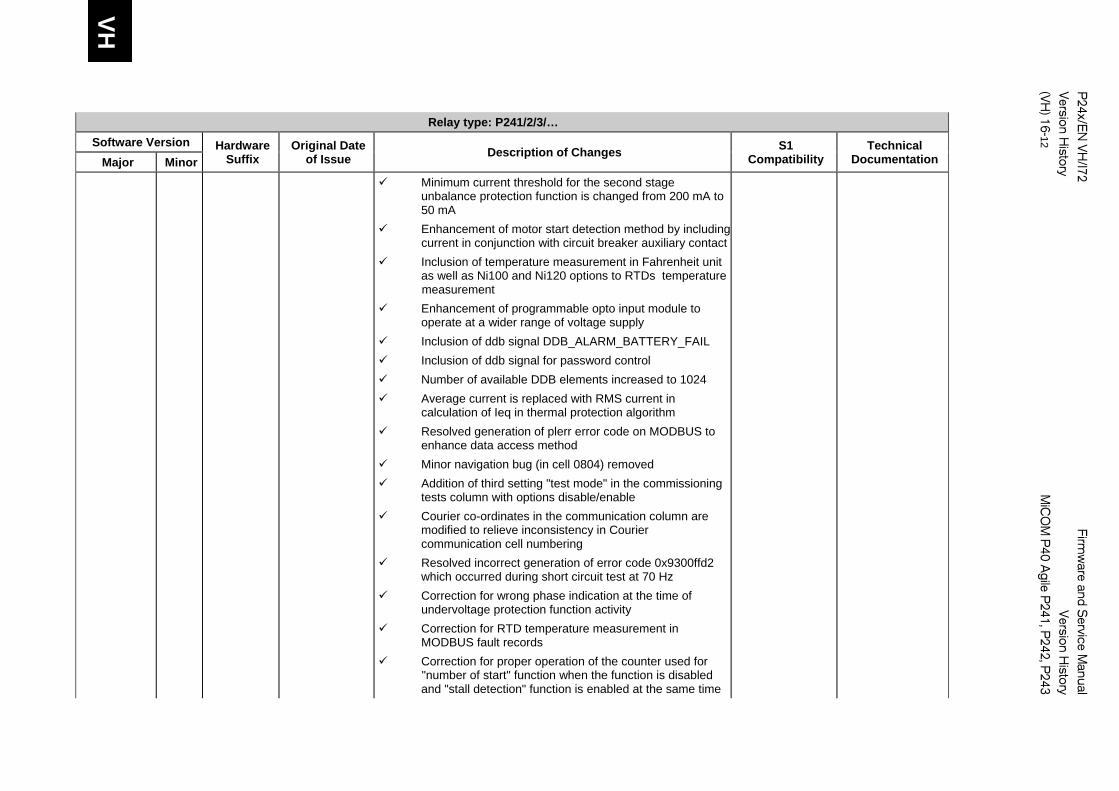
VH
P24x/E
N VH
/I72
Firmw
are and Service M
anual
Version History
Version H
istory (VH
) 16-12
MiC
OM
P40 A
gile P241, P
242, P243
Relay type: P241/2/3/…
Software Version Hardware Suffix
Original Date of Issue Description of Changes S1
Compatibility Technical
Documentation Major Minor
Minimum current threshold for the second stage unbalance protection function is changed from 200 mA to 50 mA
Enhancement of motor start detection method by including current in conjunction with circuit breaker auxiliary contact
Inclusion of temperature measurement in Fahrenheit unit as well as Ni100 and Ni120 options to RTDs temperature measurement
Enhancement of programmable opto input module to operate at a wider range of voltage supply
Inclusion of ddb signal DDB_ALARM_BATTERY_FAIL Inclusion of ddb signal for password control Number of available DDB elements increased to 1024 Average current is replaced with RMS current in
calculation of Ieq in thermal protection algorithm Resolved generation of plerr error code on MODBUS to
enhance data access method Minor navigation bug (in cell 0804) removed Addition of third setting "test mode" in the commissioning
tests column with options disable/enable Courier co-ordinates in the communication column are
modified to relieve inconsistency in Courier communication cell numbering
Resolved incorrect generation of error code 0x9300ffd2 which occurred during short circuit test at 70 Hz
Correction for wrong phase indication at the time of undervoltage protection function activity
Correction for RTD temperature measurement in MODBUS fault records
Correction for proper operation of the counter used for "number of start" function when the function is disabled and "stall detection" function is enabled at the same time

VH
Firmw
are and Service M
anual
P24x/E
N VH
/I72 Version H
istory
M
iCO
M P
40 Agile P
241, P242, P
243
(VH) 16-13
Relay type: P241/2/3/…
Software Version Hardware Suffix
Original Date of Issue Description of Changes S1
Compatibility Technical
Documentation Major Minor
Correction for proper RTD number indication when corresponding RTD trip cell is active
Correction for intermittent twice-resetting requirement of trip LED
Resolved initialization of protection/PSL programs secondary effect on LEDs and output relays
Resolved re-scaling problem for I^ maintenance and I^ lockout settings arising from a change in Broken I^ setting in the MICOM S1 setting file
Resolved incorrect timing for trip operation under second stage negative phase sequence function
Resolved zero sequence current measurement algorithm. The quantity was obtained from derived nominal current rather than measured nominal current
Correction for mal-operation of thermal over load function after battery back-up RAM initialization when no RTD module is present
Correction of the method by which negative phase sequence current magnitude is calculated when "derived E/F" function in the "configuration" column is enabled
Resolved incorrect correlation between CT ratio and derived E/F threshold
Removal of undesirable command for continuous test of EEPROM
Change of the acquisition time for thermal protection function from 50 ms to 20 ms
Resolved momentary miss-representation of positive and negative phase sequence current magnitudes and mal-functioning of first stage I2 trip function when thermal over load function is enabled
Resolved mal-operation of Derived E/F function when under test condition due to missing I2 polarizing quantity
Resolved improper dependency rules concerning RTD label in second group setting column
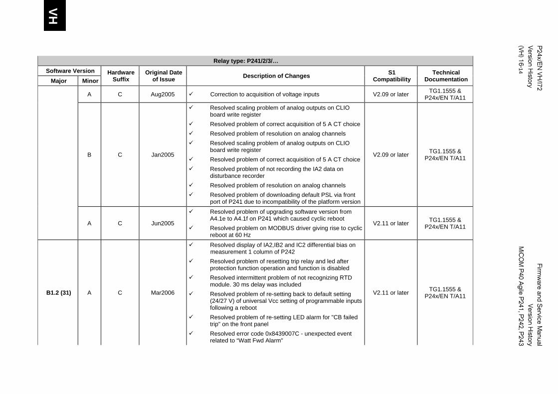
VH
P24x/E
N VH
/I72
Firmw
are and Service M
anual
Version History
Version H
istory (VH
) 16-14
MiC
OM
P40 A
gile P241, P
242, P243
Relay type: P241/2/3/…
Software Version Hardware Suffix
Original Date of Issue Description of Changes S1
Compatibility Technical
Documentation Major Minor
A C Aug2005 Correction to acquisition of voltage inputs V2.09 or later TG1.1555 & P24x/EN T/A11
B C Jan2005
Resolved scaling problem of analog outputs on CLIO board write register
Resolved problem of correct acquisition of 5 A CT choice Resolved problem of resolution on analog channels Resolved scaling problem of analog outputs on CLIO
board write register Resolved problem of correct acquisition of 5 A CT choice Resolved problem of not recording the IA2 data on
disturbance recorder Resolved problem of resolution on analog channels Resolved problem of downloading default PSL via front
port of P241 due to incompatibility of the platform version
V2.09 or later TG1.1555 & P24x/EN T/A11
A C Jun2005
Resolved problem of upgrading software version from A4.1e to A4.1f on P241 which caused cyclic reboot
Resolved problem on MODBUS driver giving rise to cyclic reboot at 60 Hz
V2.11 or later TG1.1555 & P24x/EN T/A11
B1.2 (31) A C Mar2006
Resolved display of IA2,IB2 and IC2 differential bias on measurement 1 column of P242
Resolved problem of resetting trip relay and led after protection function operation and function is disabled
Resolved intermittent problem of not recognizing RTD module. 30 ms delay was included
Resolved problem of re-setting back to default setting (24/27 V) of universal Vcc setting of programmable inputs following a reboot
Resolved problem of re-setting LED alarm for "CB failed trip" on the front panel
Resolved error code 0x8439007C - unexpected event related to “Watt Fwd Alarm"
V2.11 or later TG1.1555 & P24x/EN T/A11
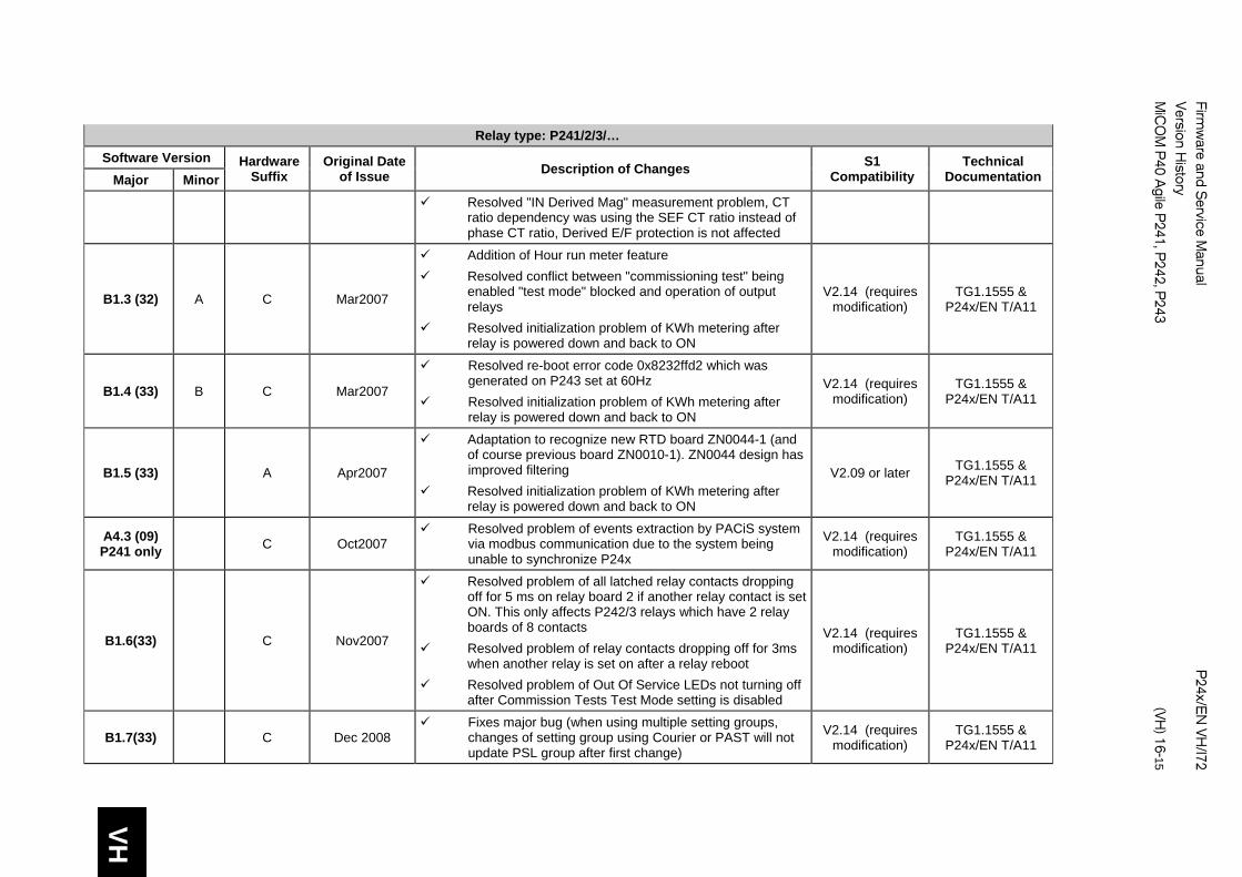
VH
Firmw
are and Service M
anual
P24x/E
N VH
/I72 Version H
istory
M
iCO
M P
40 Agile P
241, P242, P
243
(VH) 16-15
Relay type: P241/2/3/…
Software Version Hardware Suffix
Original Date of Issue Description of Changes S1
Compatibility Technical
Documentation Major Minor
Resolved "IN Derived Mag" measurement problem, CT
ratio dependency was using the SEF CT ratio instead of phase CT ratio, Derived E/F protection is not affected
B1.3 (32) A C Mar2007
Addition of Hour run meter feature Resolved conflict between "commissioning test" being
enabled "test mode" blocked and operation of output relays
Resolved initialization problem of KWh metering after relay is powered down and back to ON
V2.14 (requires modification)
TG1.1555 & P24x/EN T/A11
B1.4 (33) B C Mar2007
Resolved re-boot error code 0x8232ffd2 which was generated on P243 set at 60Hz Resolved initialization problem of KWh metering after relay is powered down and back to ON
V2.14 (requires modification)
TG1.1555 & P24x/EN T/A11
B1.5 (33) A Apr2007
Adaptation to recognize new RTD board ZN0044-1 (and of course previous board ZN0010-1). ZN0044 design has improved filtering
Resolved initialization problem of KWh metering after relay is powered down and back to ON
V2.09 or later TG1.1555 & P24x/EN T/A11
A4.3 (09) P241 only C Oct2007
Resolved problem of events extraction by PACiS system via modbus communication due to the system being unable to synchronize P24x
V2.14 (requires modification)
TG1.1555 & P24x/EN T/A11
B1.6(33) C Nov2007
Resolved problem of all latched relay contacts dropping off for 5 ms on relay board 2 if another relay contact is set ON. This only affects P242/3 relays which have 2 relay boards of 8 contacts
Resolved problem of relay contacts dropping off for 3ms when another relay is set on after a relay reboot
Resolved problem of Out Of Service LEDs not turning off after Commission Tests Test Mode setting is disabled
V2.14 (requires modification)
TG1.1555 & P24x/EN T/A11
B1.7(33) C Dec 2008 Fixes major bug (when using multiple setting groups,
changes of setting group using Courier or PAST will not update PSL group after first change)
V2.14 (requires modification)
TG1.1555 & P24x/EN T/A11
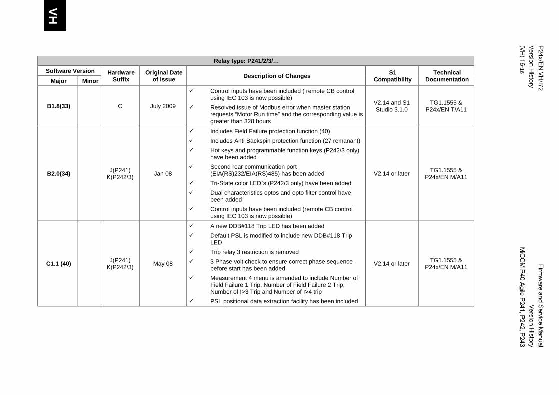
VH
P24x/E
N VH
/I72
Firmw
are and Service M
anual
Version History
Version H
istory (VH
) 16-16
MiC
OM
P40 A
gile P241, P
242, P243
Relay type: P241/2/3/…
Software Version Hardware Suffix
Original Date of Issue Description of Changes S1
Compatibility Technical
Documentation Major Minor
B1.8(33) C July 2009
Control inputs have been included ( remote CB control using IEC 103 is now possible)
Resolved issue of Modbus error when master station requests “Motor Run time” and the corresponding value is greater than 328 hours
V2.14 and S1 Studio 3.1.0
TG1.1555 & P24x/EN T/A11
B2.0(34) J(P241) K(P242/3) Jan 08
Includes Field Failure protection function (40) Includes Anti Backspin protection function (27 remanant) Hot keys and programmable function keys (P242/3 only)
have been added Second rear communication port
(EIA(RS)232/EIA(RS)485) has been added Tri-State color LED`s (P242/3 only) have been added Dual characteristics optos and opto filter control have
been added Control inputs have been included (remote CB control
using IEC 103 is now possible)
V2.14 or later TG1.1555 & P24x/EN M/A11
C1.1 (40) J(P241) K(P242/3) May 08
A new DDB#118 Trip LED has been added Default PSL is modified to include new DDB#118 Trip
LED Trip relay 3 restriction is removed 3 Phase volt check to ensure correct phase sequence
before start has been added Measurement 4 menu is amended to include Number of
Field Failure 1 Trip, Number of Field Failure 2 Trip, Number of I>3 Trip and Number of I>4 trip
PSL positional data extraction facility has been included
V2.14 or later
TG1.1555 & P24x/EN M/A11
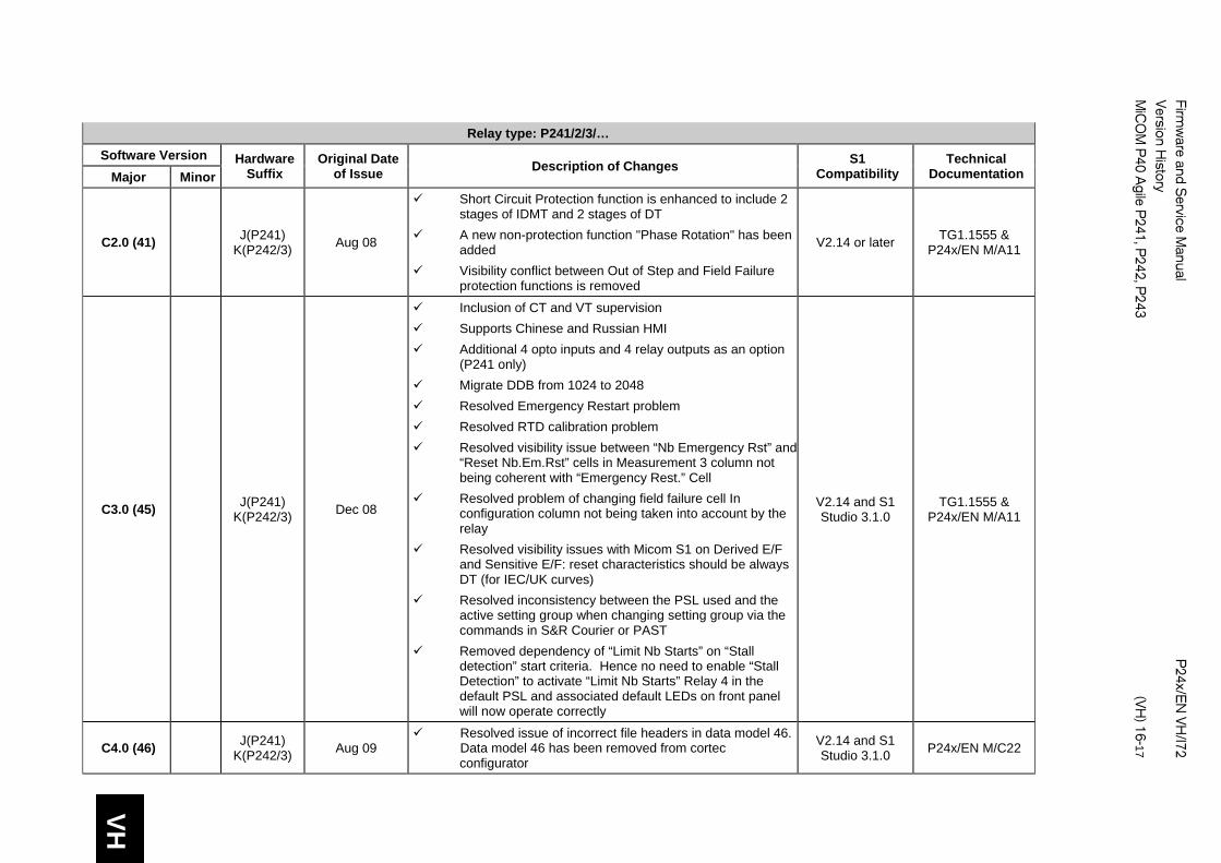
VH
Firmw
are and Service M
anual
P24x/E
N VH
/I72 Version H
istory
M
iCO
M P
40 Agile P
241, P242, P
243
(VH) 16-17
Relay type: P241/2/3/…
Software Version Hardware Suffix
Original Date of Issue Description of Changes S1
Compatibility Technical
Documentation Major Minor
C2.0 (41) J(P241) K(P242/3) Aug 08
Short Circuit Protection function is enhanced to include 2 stages of IDMT and 2 stages of DT
A new non-protection function "Phase Rotation" has been added
Visibility conflict between Out of Step and Field Failure protection functions is removed
V2.14 or later
TG1.1555 & P24x/EN M/A11
C3.0 (45) J(P241) K(P242/3) Dec 08
Inclusion of CT and VT supervision Supports Chinese and Russian HMI Additional 4 opto inputs and 4 relay outputs as an option
(P241 only) Migrate DDB from 1024 to 2048 Resolved Emergency Restart problem Resolved RTD calibration problem Resolved visibility issue between “Nb Emergency Rst” and
“Reset Nb.Em.Rst” cells in Measurement 3 column not being coherent with “Emergency Rest.” Cell
Resolved problem of changing field failure cell In configuration column not being taken into account by the relay
Resolved visibility issues with Micom S1 on Derived E/F and Sensitive E/F: reset characteristics should be always DT (for IEC/UK curves)
Resolved inconsistency between the PSL used and the active setting group when changing setting group via the commands in S&R Courier or PAST
Removed dependency of “Limit Nb Starts” on “Stall detection” start criteria. Hence no need to enable “Stall Detection” to activate “Limit Nb Starts” Relay 4 in the default PSL and associated default LEDs on front panel will now operate correctly
V2.14 and S1 Studio 3.1.0
TG1.1555 & P24x/EN M/A11
C4.0 (46) J(P241) K(P242/3) Aug 09
Resolved issue of incorrect file headers in data model 46. Data model 46 has been removed from cortec configurator
V2.14 and S1 Studio 3.1.0 P24x/EN M/C22
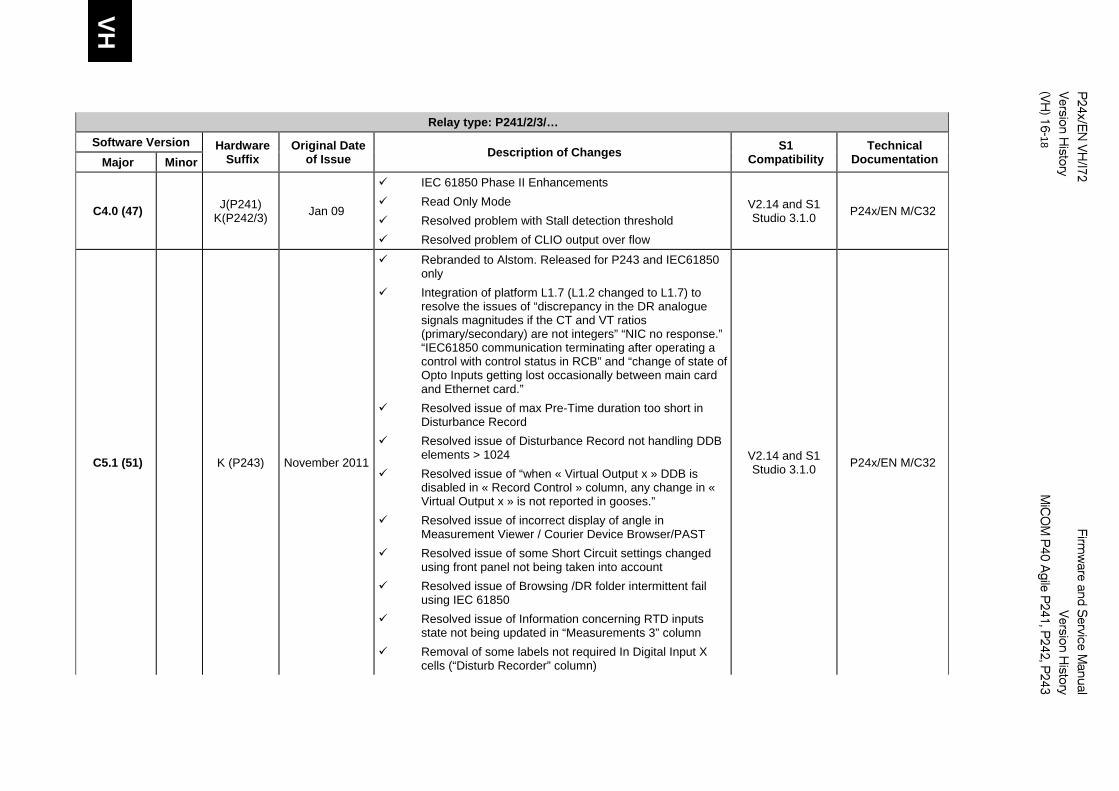
VH
P24x/E
N VH
/I72
Firmw
are and Service M
anual
Version History
Version H
istory (VH
) 16-18
MiC
OM
P40 A
gile P241, P
242, P243
Relay type: P241/2/3/…
Software Version Hardware Suffix
Original Date of Issue Description of Changes S1
Compatibility Technical
Documentation Major Minor
C4.0 (47) J(P241) K(P242/3) Jan 09
IEC 61850 Phase II Enhancements Read Only Mode Resolved problem with Stall detection threshold Resolved problem of CLIO output over flow
V2.14 and S1 Studio 3.1.0 P24x/EN M/C32
C5.1 (51) K (P243) November 2011
Rebranded to Alstom. Released for P243 and IEC61850 only
Integration of platform L1.7 (L1.2 changed to L1.7) to resolve the issues of “discrepancy in the DR analogue signals magnitudes if the CT and VT ratios (primary/secondary) are not integers” “NIC no response.” “IEC61850 communication terminating after operating a control with control status in RCB” and “change of state of Opto Inputs getting lost occasionally between main card and Ethernet card.”
Resolved issue of max Pre-Time duration too short in Disturbance Record
Resolved issue of Disturbance Record not handling DDB elements > 1024
Resolved issue of “when « Virtual Output x » DDB is disabled in « Record Control » column, any change in « Virtual Output x » is not reported in gooses.”
Resolved issue of incorrect display of angle in Measurement Viewer / Courier Device Browser/PAST
Resolved issue of some Short Circuit settings changed using front panel not being taken into account
Resolved issue of Browsing /DR folder intermittent fail using IEC 61850
Resolved issue of Information concerning RTD inputs state not being updated in “Measurements 3” column
Removal of some labels not required In Digital Input X cells (“Disturb Recorder” column)
V2.14 and S1 Studio 3.1.0 P24x/EN M/C32
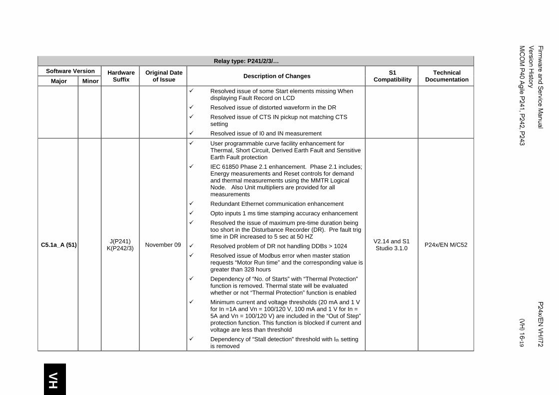
VH
Firmw
are and Service M
anual
P24x/E
N VH
/I72 Version H
istory
M
iCO
M P
40 Agile P
241, P242, P
243
(VH) 16-19
Relay type: P241/2/3/…
Software Version Hardware Suffix
Original Date of Issue Description of Changes S1
Compatibility Technical
Documentation Major Minor
Resolved issue of some Start elements missing When displaying Fault Record on LCD
Resolved issue of distorted waveform in the DR Resolved issue of CTS IN pickup not matching CTS
setting Resolved issue of I0 and IN measurement
C5.1a_A (51) J(P241) K(P242/3) November 09
User programmable curve facility enhancement for Thermal, Short Circuit, Derived Earth Fault and Sensitive Earth Fault protection
IEC 61850 Phase 2.1 enhancement. Phase 2.1 includes; Energy measurements and Reset controls for demand and thermal measurements using the MMTR Logical Node. Also Unit multipliers are provided for all measurements
Redundant Ethernet communication enhancement Opto inputs 1 ms time stamping accuracy enhancement Resolved the issue of maximum pre-time duration being
too short in the Disturbance Recorder (DR). Pre fault trig time in DR increased to 5 sec at 50 HZ
Resolved problem of DR not handling DDBs > 1024 Resolved issue of Modbus error when master station
requests “Motor Run time” and the corresponding value is greater than 328 hours
Dependency of “No. of Starts” with “Thermal Protection” function is removed. Thermal state will be evaluated whether or not “Thermal Protection” function is enabled
Minimum current and voltage thresholds (20 mA and 1 V for In =1A and Vn = 100/120 V, 100 mA and 1 V for In = 5A and Vn = 100/120 V) are included in the “Out of Step” protection function. This function is blocked if current and voltage are less than threshold
Dependency of “Stall detection” threshold with Ith setting is removed
V2.14 and S1 Studio 3.1.0 P24x/EN M/C52
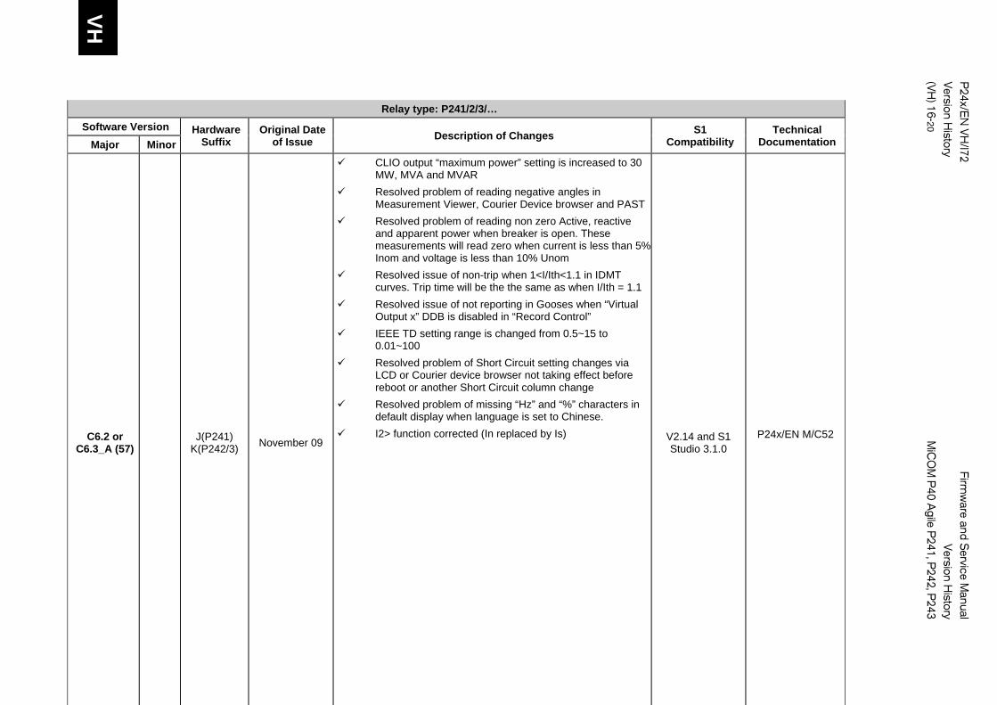
VH
P24x/E
N VH
/I72
Firmw
are and Service M
anual
Version History
Version H
istory (VH
) 16-20
MiC
OM
P40 A
gile P241, P
242, P243
Relay type: P241/2/3/…
Software Version Hardware Suffix
Original Date of Issue Description of Changes S1
Compatibility Technical
Documentation Major Minor
C6.2 or C6.3_A (57) J(P241)
K(P242/3) November 09
CLIO output “maximum power” setting is increased to 30 MW, MVA and MVAR
Resolved problem of reading negative angles in Measurement Viewer, Courier Device browser and PAST
Resolved problem of reading non zero Active, reactive and apparent power when breaker is open. These measurements will read zero when current is less than 5% Inom and voltage is less than 10% Unom
Resolved issue of non-trip when 1<I/Ith<1.1 in IDMT curves. Trip time will be the the same as when I/Ith = 1.1
Resolved issue of not reporting in Gooses when “Virtual Output x” DDB is disabled in “Record Control”
IEEE TD setting range is changed from 0.5~15 to 0.01~100
Resolved problem of Short Circuit setting changes via LCD or Courier device browser not taking effect before reboot or another Short Circuit column change
Resolved problem of missing “Hz” and “%” characters in default display when language is set to Chinese.
I2> function corrected (In replaced by Is)
V2.14 and S1 Studio 3.1.0
P24x/EN M/C52
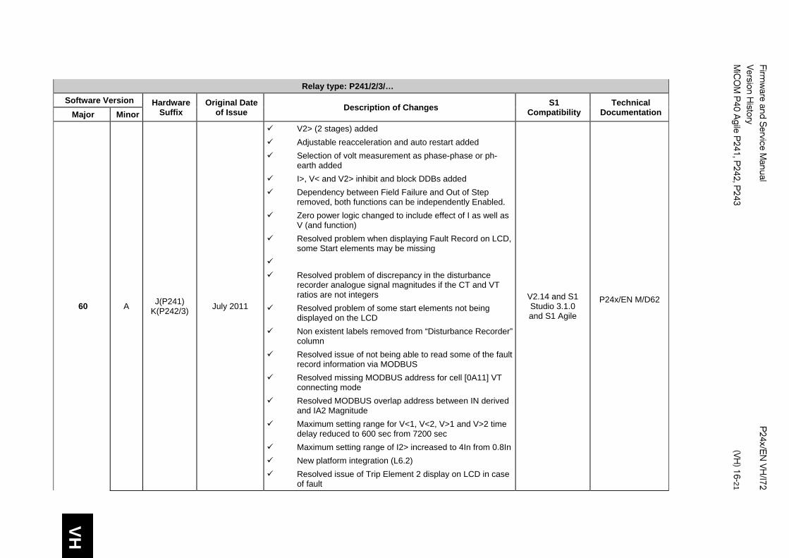
VH
Firmw
are and Service M
anual
P24x/E
N VH
/I72 Version H
istory
M
iCO
M P
40 Agile P
241, P242, P
243
(VH) 16-21
Relay type: P241/2/3/…
Software Version Hardware Suffix
Original Date of Issue Description of Changes S1
Compatibility Technical
Documentation Major Minor
60 A J(P241) K(P242/3) July 2011
V2> (2 stages) added Adjustable reacceleration and auto restart added Selection of volt measurement as phase-phase or ph-
earth added I>, V< and V2> inhibit and block DDBs added Dependency between Field Failure and Out of Step
removed, both functions can be independently Enabled. Zero power logic changed to include effect of I as well as
V (and function) Resolved problem when displaying Fault Record on LCD,
some Start elements may be missing Resolved problem of discrepancy in the disturbance
recorder analogue signal magnitudes if the CT and VT ratios are not integers
Resolved problem of some start elements not being displayed on the LCD
Non existent labels removed from “Disturbance Recorder” column
Resolved issue of not being able to read some of the fault record information via MODBUS
Resolved missing MODBUS address for cell [0A11] VT connecting mode
Resolved MODBUS overlap address between IN derived and IA2 Magnitude
Maximum setting range for V<1, V<2, V>1 and V>2 time delay reduced to 600 sec from 7200 sec
Maximum setting range of I2> increased to 4In from 0.8In New platform integration (L6.2) Resolved issue of Trip Element 2 display on LCD in case
of fault
V2.14 and S1 Studio 3.1.0 and S1 Agile
P24x/EN M/D62
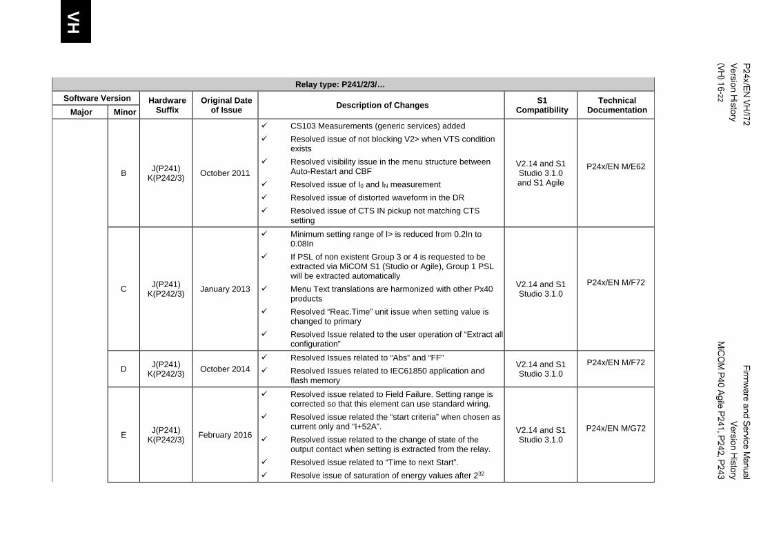
VH
P24x/E
N VH
/I72
Firmw
are and Service M
anual
Version History
Version H
istory (VH
) 16-22
MiC
OM
P40 A
gile P241, P
242, P243
Relay type: P241/2/3/…
Software Version Hardware Suffix
Original Date of Issue Description of Changes S1
Compatibility Technical
Documentation Major Minor
B J(P241) K(P242/3) October 2011
CS103 Measurements (generic services) added Resolved issue of not blocking V2> when VTS condition
exists Resolved visibility issue in the menu structure between
Auto-Restart and CBF Resolved issue of I0 and IN measurement Resolved issue of distorted waveform in the DR Resolved issue of CTS IN pickup not matching CTS
setting
V2.14 and S1 Studio 3.1.0 and S1 Agile
P24x/EN M/E62
C J(P241) K(P242/3) January 2013
Minimum setting range of I> is reduced from 0.2In to 0.08In
If PSL of non existent Group 3 or 4 is requested to be extracted via MiCOM S1 (Studio or Agile), Group 1 PSL will be extracted automatically
Menu Text translations are harmonized with other Px40 products
Resolved “Reac.Time” unit issue when setting value is changed to primary
Resolved Issue related to the user operation of “Extract all configuration”
V2.14 and S1 Studio 3.1.0
P24x/EN M/F72
D J(P241) K(P242/3) October 2014
Resolved Issues related to “Abs” and “FF” Resolved Issues related to IEC61850 application and
flash memory
V2.14 and S1 Studio 3.1.0
P24x/EN M/F72
E J(P241) K(P242/3) February 2016
Resolved issue related to Field Failure. Setting range is corrected so that this element can use standard wiring.
Resolved issue related the “start criteria” when chosen as current only and “I+52A”.
Resolved issue related to the change of state of the output contact when setting is extracted from the relay.
Resolved issue related to “Time to next Start”. Resolve issue of saturation of energy values after 232
V2.14 and S1 Studio 3.1.0
P24x/EN M/G72
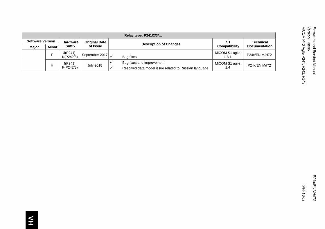
VH
Firmw
are and Service M
anual
P24x/E
N VH
/I72 Version H
istory
M
iCO
M P
40 Agile P
241, P242, P
243
(VH) 16-23
Relay type: P241/2/3/…
Software Version Hardware Suffix
Original Date of Issue Description of Changes S1
Compatibility Technical
Documentation Major Minor
F J(P241) K(P242/3) September 2017
Bug fixes MiCOM S1 agile
1.3.1 P24x/EN M/H72
H J(P241) K(P242/3) July 2018
Bug fixes and improvement Resolved data model issue related to Russian language
MiCOM S1 agile 1.4 P24x/EN M/I72
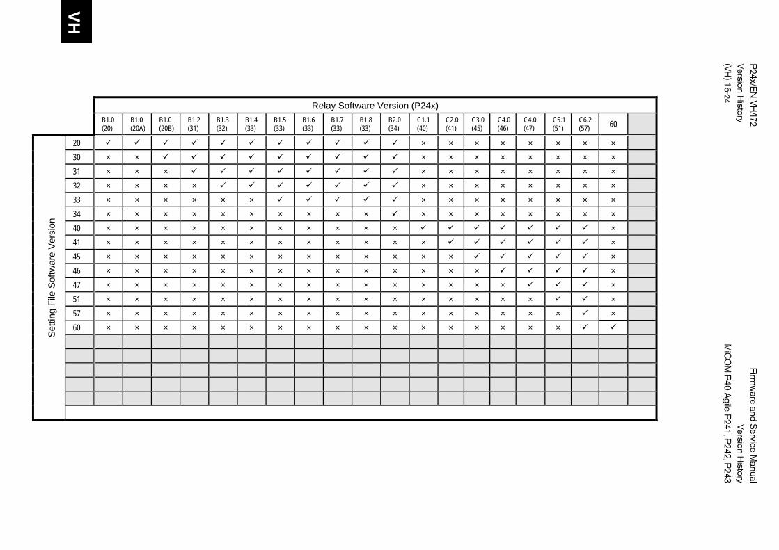
VH
P24x/E
N VH
/I72
Firmw
are and Service M
anual
Version History
Version H
istory (VH
) 16-24
MiC
OM
P40 A
gile P241, P
242, P243
Relay Software Version (P24x)
B1.0 (20)
B1.0 (20A)
B1.0 (20B)
B1.2 (31)
B1.3 (32)
B1.4 (33)
B1.5 (33)
B1.6 (33)
B1.7 (33)
B1.8 (33)
B2.0 (34)
C1.1 (40)
C2.0 (41)
C3.0 (45)
C4.0 (46)
C4.0 (47)
C5.1 (51)
C6.2 (57) 60
Setti
ng F
ile S
oftw
are
Vers
ion
20 × × × × × × × ×
30 × × × × × × × × × ×
31 × × × × × × × × × × ×
32 × × × × × × × × × × × ×
33 × × × × × × × × × × × × × ×
34 × × × × × × × × × × × × × × × × × ×
40 × × × × × × × × × × × ×
41 × × × × × × × × × × × × ×
45 × × × × × × × × × × × × × ×
46 × × × × × × × × × × × × × × ×
47 × × × × × × × × × × × × × × × ×
51 × × × × × × × × × × × × × × × × ×
57 × × × × × × × × × × × × × × × × × ×
60 × × × × × × × × × × × × × × × × ×
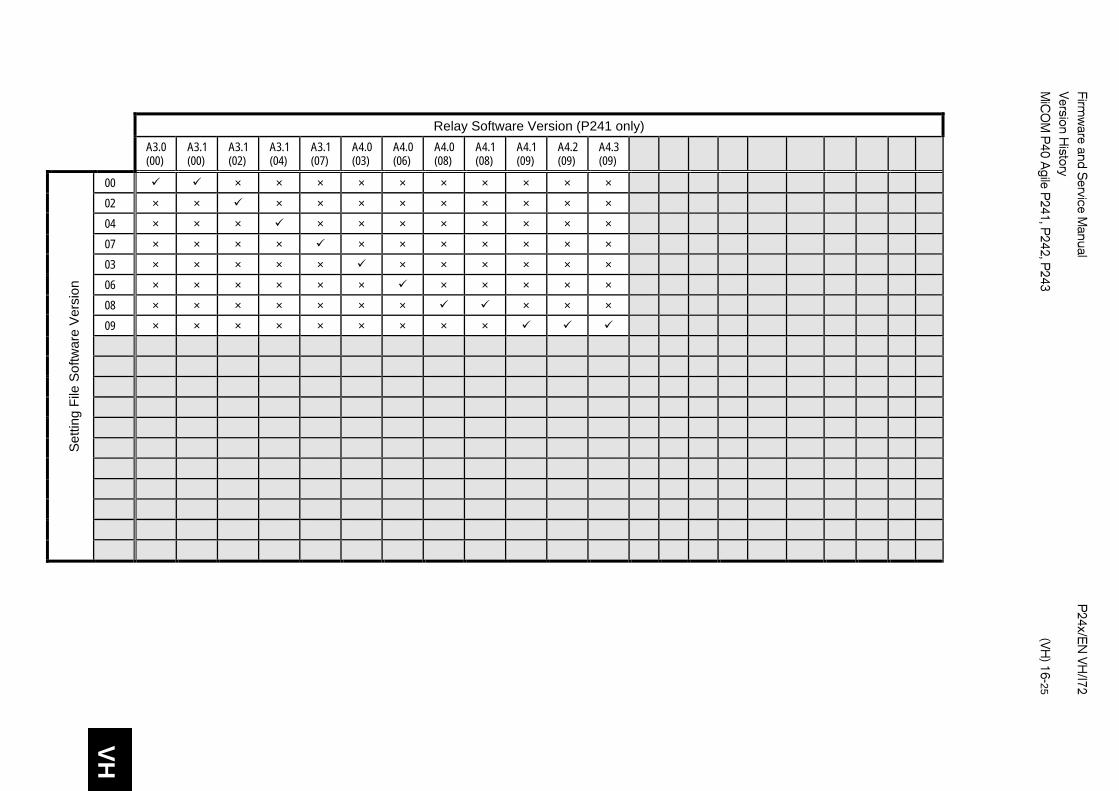
VH
Firmw
are and Service M
anual
P24x/E
N VH
/I72 Version H
istory
M
iCO
M P
40 Agile P
241, P242, P
243
(VH) 16-25
Relay Software Version (P241 only)
A3.0(00)
A3.1(00)
A3.1(02)
A3.1(04)
A3.1(07)
A4.0(03)
A4.0(06)
A4.0 (08)
A4.1 (08)
A4.1 (09)
A4.2 (09)
A4.3(09)
Setti
ng F
ile S
oftw
are
Vers
ion
00 × × × × × × × × × ×
02 × × × × × × × × × × ×
04 × × × × × × × × × × ×
07 × × × × × × × × × × ×
03 × × × × × × × × × × ×
06 × × × × × × × × × × ×
08 × × × × × × × × × ×
09 × × × × × × × × ×
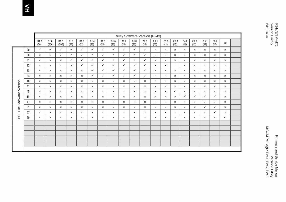
VH
P24x/E
N VH
/I72
Firmw
are and Service M
anual
Version History
Version H
istory (VH
) 16-26
MiC
OM
P40 A
gile P241, P
242, P243
Relay Software Version (P24x)
B1.0 (20)
B1.0 (20A)
B1.0 (20B)
B1.2 (31)
B1.3 (32)
B1.4 (33)
B1.5 (33)
B1.6 (33)
B1.7 (33)
B1.8 (33)
B2.0 (34)
C1.1 (40)
C2.0 (41)
C3.0 (45)
C4.0 (46)
C4.0 (47)
C5.1 (51)
C6.2 (57) 60
PSL
File
Sof
twar
e Ve
rsio
n
20 × × × × × × × ×
30 × × × × × × × × × ×
31 × × × × × × × × × × ×
32 × × × × × × × × × × × ×
33 × × × × × × × × × × × × ×
34 × × × × × × × × × × × × ×
40 × × × × × × × × × × × × × × × × ×
41 × × × × × × × × × × × × × × × × × ×
45 × × × × × × × × × × × × × × × × × ×
46 × × × × × × × × × × × × × × ×
47 × × × × × × × × × × × × × × × ×
51 × × × × × × × × × × × × × × × × ×
57 × × × × × × × × × × × × × × × × × ×
60 × × × × × × × × × × × × × × × × × ×
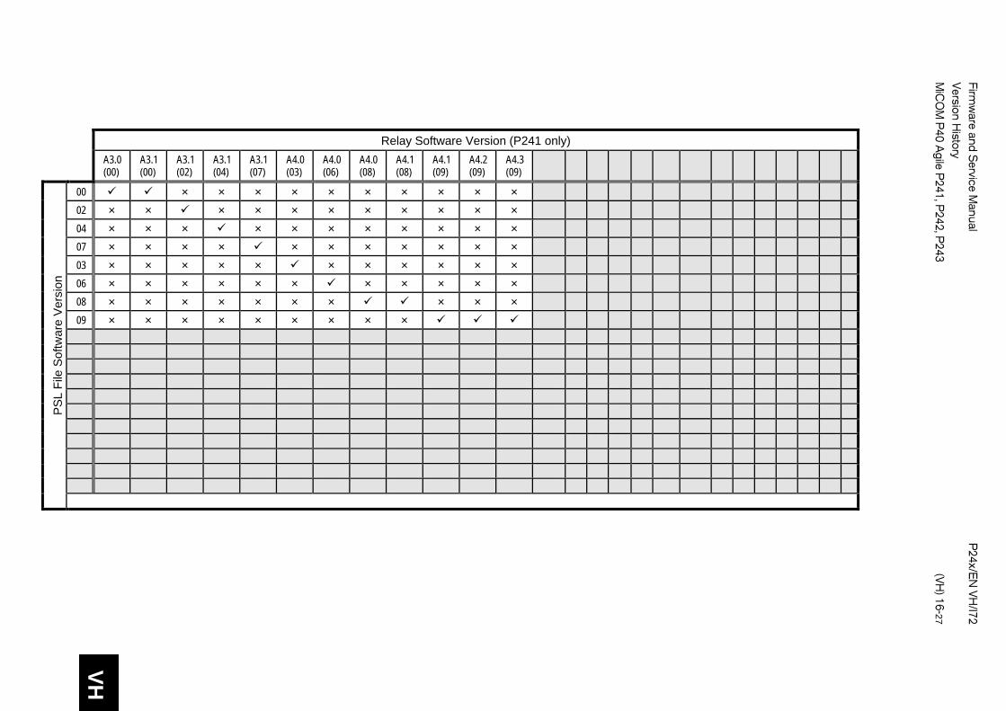
VH
Firmw
are and Service M
anual
P24x/E
N VH
/I72 Version H
istory
M
iCO
M P
40 Agile P
241, P242, P
243
(VH) 16-27
Relay Software Version (P241 only)
A3.0 (00)
A3.1 (00)
A3.1(02)
A3.1(04)
A3.1(07)
A4.0(03)
A4.0(06)
A4.0 (08)
A4.1 (08)
A4.1 (09)
A4.2 (09)
A4.3 (09)
PSL
File
Sof
twar
e Ve
rsio
n
00 × × × × × × × × × × 02 × × × × × × × × × × × 04 × × × × × × × × × × × 07 × × × × × × × × × × × 03 × × × × × × × × × × × 06 × × × × × × × × × × × 08 × × × × × × × × × × 09 × × × × × × × × ×
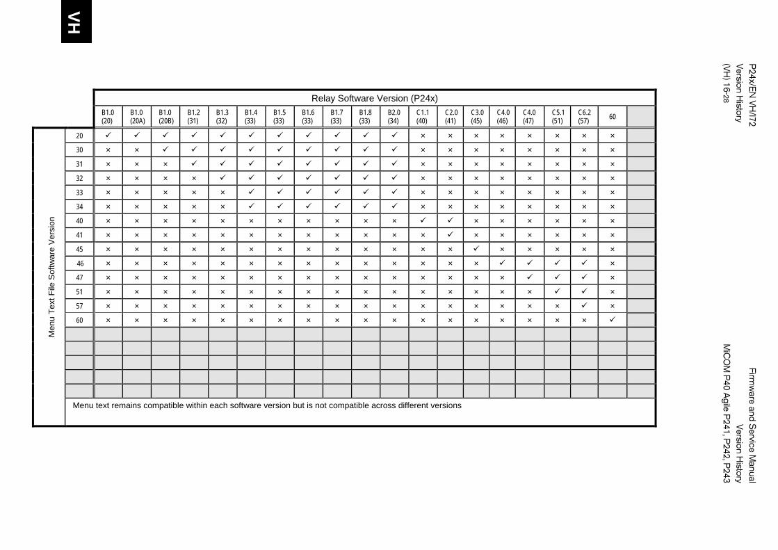
VH
P24x/E
N VH
/I72
Firmw
are and Service M
anual
Version History
Version H
istory (VH
) 16-28
MiC
OM
P40 A
gile P241, P
242, P243
Relay Software Version (P24x)
B1.0 (20)
B1.0 (20A)
B1.0 (20B)
B1.2 (31)
B1.3 (32)
B1.4 (33)
B1.5 (33)
B1.6 (33)
B1.7 (33)
B1.8 (33)
B2.0 (34)
C1.1 (40)
C2.0 (41)
C3.0 (45)
C4.0 (46)
C4.0 (47)
C5.1 (51)
C6.2 (57) 60
Men
u Te
xt F
ile S
oftw
are
Ver
sion
20 × × × × × × × ×
30 × × × × × × × × × ×
31 × × × × × × × × × × ×
32 × × × × × × × × × × × ×
33 × × × × × × × × × × × × ×
34 × × × × × × × × × × × × ×
40 × × × × × × × × × × × × × × × × ×
41 × × × × × × × × × × × × × × × × × ×
45 × × × × × × × × × × × × × × × × × ×
46 × × × × × × × × × × × × × × ×
47 × × × × × × × × × × × × × × × ×
51 × × × × × × × × × × × × × × × × ×
57 × × × × × × × × × × × × × × × × × ×
60 × × × × × × × × × × × × × × × × × ×
Menu text remains compatible within each software version but is not compatible across different versions
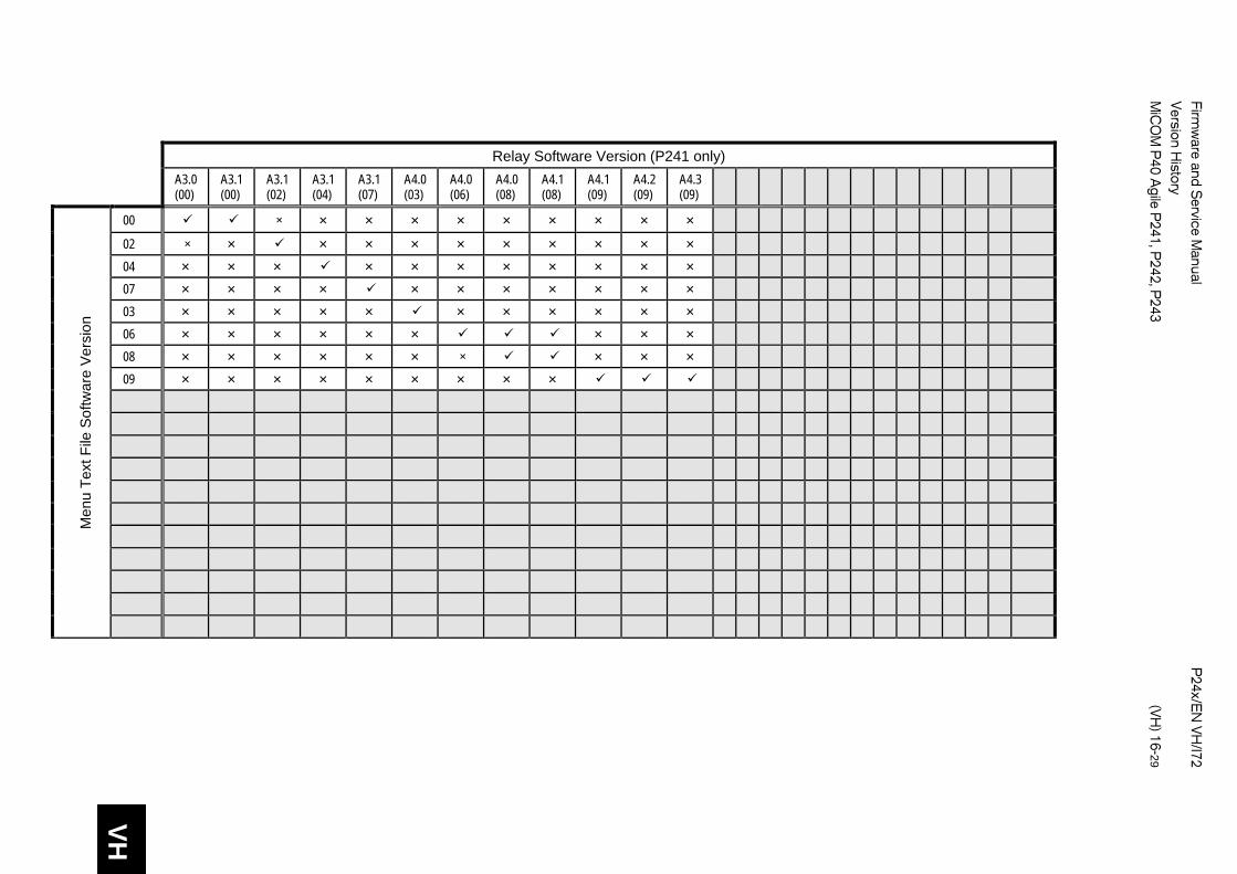
VH
Firmw
are and Service M
anual
P24x/E
N VH
/I72 Version H
istory
M
iCO
M P
40 Agile P
241, P242, P
243
(VH) 16-29
Relay Software Version (P241 only)
A3.0(00)
A3.1(00)
A3.1(02)
A3.1(04)
A3.1(07)
A4.0(03)
A4.0(06)
A4.0 (08)
A4.1 (08)
A4.1 (09)
A4.2 (09)
A4.3 (09)
Men
u Te
xt F
ile S
oftw
are
Vers
ion
00 × × × × × × × × × ×
02 × × × × × × × × × × × 04 × × × × × × × × × × × 07 × × × × × × × × × × × 03 × × × × × × × × × × × 06 × × × × × × × × × 08 × × × × × × × × × × 09 × × × × × × × × ×


Imagination at work
Grid Solutions St Leonards Building Redhill Business Park Stafford, ST16 1WT, UK +44 (0) 1785 250 070 www.gegridsolutions.com/contact
© 2018 General Electric. All rights reserved. Information contained in this document is indicative only. No representation or warranty is given or should be relied on that it is complete or correct or will apply to any particular project. This will depend on the technical and commercial circumstances. It is provided without liability and is subject to change without notice. Reproduction, use or disclosure to third parties, without express written authority, is strictly prohibited.
P24x/EN M/I72


![CONSULTATION PAPER PROPOSAL P242 FOOD FOR SPECIAL … · 2018. 6. 26. · i 15 December 2010 [25-10] CONSULTATION PAPER PROPOSAL P242 FOOD FOR SPECIAL MEDICAL PURPOSES DEADLINE FOR](https://img.pdfslide.us/doc/110x75/60d9b016a5f77b5ca2102382/consultation-paper-proposal-p242-food-for-special-2018-6-26-i-15-december-2010.jpg)