Embed Size (px)
Citation preview
1. General description
Migrate classic contactless smart card systems to the next security level with the next evolution of the proven MIFARE Plus product family. MIFARE Plus EV1 brings benchmark security and additional features to mainstream contactless smart card applications. It is the only mainstream IC compatible with MIFARE Classic EV1 1K (MF1S50yyX/V1), MIFARE Classic EV1 4K (MF1S70yyX/V1) and the MIFARE Plus EV0 product family (MF1PLUSx0y1 and MF1SPLUSx0y1) which offers a seamless upgrade path for existing infrastructure and services.
MIFARE Plus EV1 enables system operators to selectively upgrade security relevant applications. The ability to operate non-security relevant applications on existing CRYPTO1 infrastructure minimizes total cost of ownership (TCO) for the whole infrastructure eco-system. After switching to Security Level 3, MIFARE Plus EV1 uses Advanced Encryption Standard (AES) based on open global standards for cryptographic methods for authentication, data integrity protection and data encryption.
Variants with EEPROM sizes up to 4K cater for the growing number of contactless applications and thus growing memory needs. This support empowers system operators to add future applications as needed while relying on an established product standard. The use of the MIFARE Application Directory (MAD) simplifies the future on-boarding of new applications on a MIFARE Plus EV1, see Ref. 5.
AES for data encryption and integrity protection is also used for the secure end-to-end channel communication capabilities of MIFARE Plus EV1. This new evolution allows system operators to remotely manage card content over-the-air, even for Crypto1 operated applications. Additional applications and services can thus be created remotely after card issuance in a secure way, further enhancing TCO.
The Transaction MAC feature securely verifies the authenticity of a transaction. In example for systems with multiple service providers that are using the same wallet and clearing service, the Transaction MAC feature proves to the clearing house that transactions between service providers and customers are genuine. It can also be used to verify transactions in numerous offline scenarios or where real-time online authentication capabilities are not feasible for system operators.
For easy integration with mobile devices and other convergence media, MIFARE Plus EV1 also supports communication via ISO/IEC 7816-4 APDUs. To increase flexibility, system can freely choose to communicate in the native and APDU mode.
MF1P(H)x1y1MIFARE Plus EV1Rev. 2.0 — 14 April 2016366920
Preliminary short data sheetCOMPANY PUBLIC
NXP Semiconductors MF1P(H)x1y1MIFARE Plus EV1
2. Features and benefits
2 kB, 4 kB EEPROM
7-byte UID, 4-byte NUID
Supports ISO/IEC 14443-31 Random ID for all UID types
Communication speed up to 848 kbps
Freely configurable access conditions
Security Level (SL) concept for seamless migration from legacy infrastructure to high level SL3 security
Sequential writing of the personalization keys (in SL0)
AES-128 cryptography for authentication and secure messaging (optional in SL1, mandatory in SL3)
SL3 CardSecurityLevel or sector-by-sector security level upgrade possible (SectorSecurityLevel)
SL1SL3Mix mode to allow secure back-end connections into SL1 sectors
Multi-sector authentication, multi-block read and write
Anti-tearing mechanism for AES keys, sector trailers, configuration and optionally for data block writing
Virtual card concept using ISO/IEC 7816-4 compliant selection method
Proximity check fully ISO/IEC 14443-3 compliant
Transaction MAC on value and data blocks
Direct commit personalization from SL0 to SL1 or SL3
Common Criteria Certification: EAL5+ targeted
ECC Originality signature
3. Applications
Public transportation
Access management
Electronic toll collection
Loyalty and micro-payment
1. ISO/IEC 14443-x used in this data-sheet refers to ISO/IEC 14443 Type A.
MF1P(H)x1y1_SDS All information provided in this document is subject to legal disclaimers. © NXP Semiconductors N.V. 2016. All rights reserved.
Preliminary short data sheetCOMPANY PUBLIC
Rev. 2.0 — 14 April 2016366920 2 of 26
NXP Semiconductors MF1P(H)x1y1MIFARE Plus EV1
4. Quick reference data
Remark: all values are target values only and subject to change until final product release.
Table 1. Quick reference data
Symbol Parameter Conditions Min Typ Max Unit
Ci input capacitance MF1P1y1
Tamb = 25C; fi = 13.56 MHz; 1.5V RMS
16.15 17 17.85 pF
input capacitance MF1PHx1y1
Tamb = 25C; fi = 13.56 MHz; 1.5V RMS
66.5 70 73.5 pF
fi input frequency - 13.56 - MHz
EEPROM characteristics
tret retention time Tamb = 22 C 25 - - year
Nendu(W) write endurance Tamb = 22 C; excluding anti-tearing for AES keys or sector trailers in SL 3
200000 500000 - cycle
MF1P(H)x1y1_SDS All information provided in this document is subject to legal disclaimers. © NXP Semiconductors N.V. 2016. All rights reserved.
Preliminary short data sheetCOMPANY PUBLIC
Rev. 2.0 — 14 April 2016366920 3 of 26
NXP Semiconductors MF1P(H)x1y1MIFARE Plus EV1
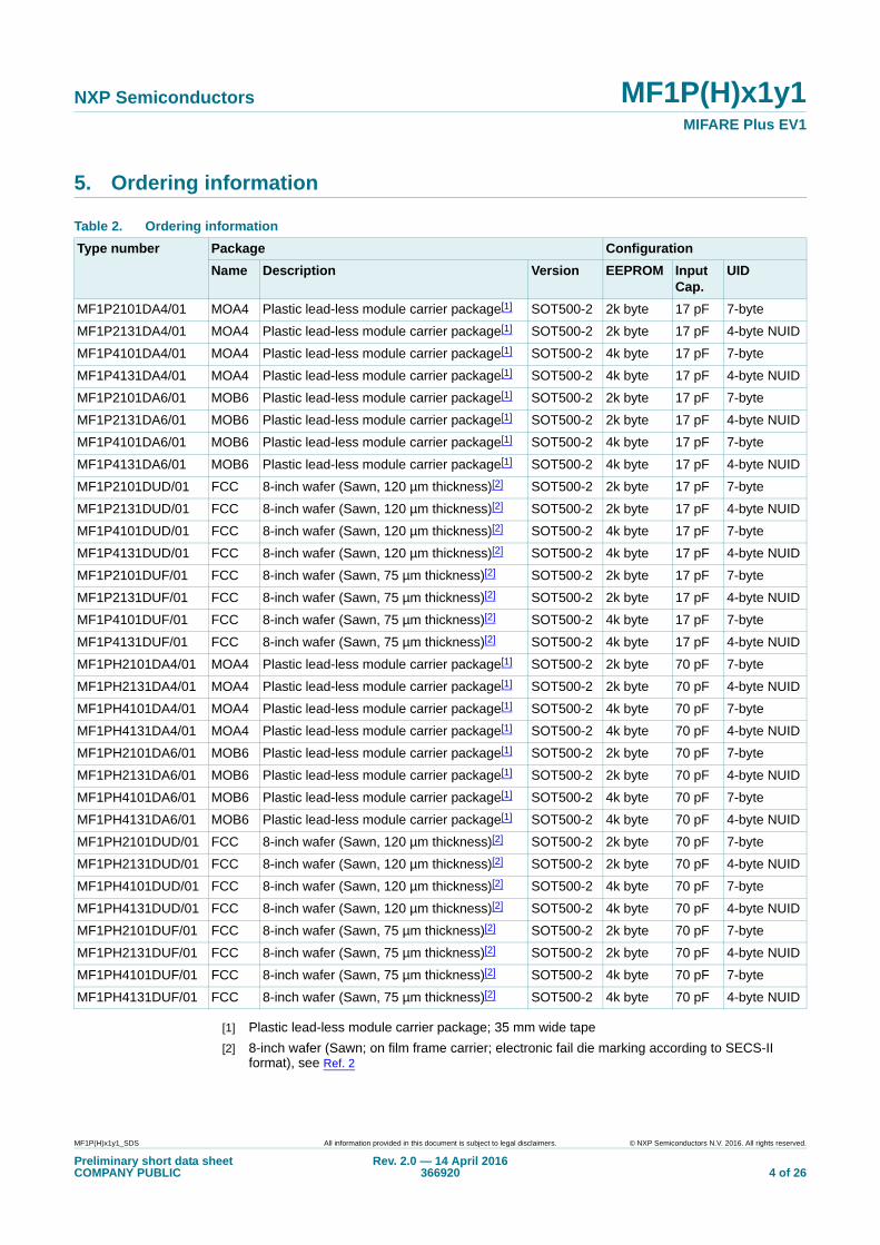
5. Ordering information
[1] Plastic lead-less module carrier package; 35 mm wide tape
[2] 8-inch wafer (Sawn; on film frame carrier; electronic fail die marking according to SECS-II format), see Ref. 2
Table 2. Ordering information
Type number Package Configuration
Name Description Version EEPROM Input Cap.
UID
MF1P2101DA4/01 MOA4 Plastic lead-less module carrier package[1] SOT500-2 2k byte 17 pF 7-byte
MF1P2131DA4/01 MOA4 Plastic lead-less module carrier package[1] SOT500-2 2k byte 17 pF 4-byte NUID
MF1P4101DA4/01 MOA4 Plastic lead-less module carrier package[1] SOT500-2 4k byte 17 pF 7-byte
MF1P4131DA4/01 MOA4 Plastic lead-less module carrier package[1] SOT500-2 4k byte 17 pF 4-byte NUID
MF1P2101DA6/01 MOB6 Plastic lead-less module carrier package[1] SOT500-2 2k byte 17 pF 7-byte
MF1P2131DA6/01 MOB6 Plastic lead-less module carrier package[1] SOT500-2 2k byte 17 pF 4-byte NUID
MF1P4101DA6/01 MOB6 Plastic lead-less module carrier package[1] SOT500-2 4k byte 17 pF 7-byte
MF1P4131DA6/01 MOB6 Plastic lead-less module carrier package[1] SOT500-2 4k byte 17 pF 4-byte NUID
MF1P2101DUD/01 FCC 8-inch wafer (Sawn, 120 µm thickness)[2] SOT500-2 2k byte 17 pF 7-byte
MF1P2131DUD/01 FCC 8-inch wafer (Sawn, 120 µm thickness)[2] SOT500-2 2k byte 17 pF 4-byte NUID
MF1P4101DUD/01 FCC 8-inch wafer (Sawn, 120 µm thickness)[2] SOT500-2 4k byte 17 pF 7-byte
MF1P4131DUD/01 FCC 8-inch wafer (Sawn, 120 µm thickness)[2] SOT500-2 4k byte 17 pF 4-byte NUID
MF1P2101DUF/01 FCC 8-inch wafer (Sawn, 75 µm thickness)[2] SOT500-2 2k byte 17 pF 7-byte
MF1P2131DUF/01 FCC 8-inch wafer (Sawn, 75 µm thickness)[2] SOT500-2 2k byte 17 pF 4-byte NUID
MF1P4101DUF/01 FCC 8-inch wafer (Sawn, 75 µm thickness)[2] SOT500-2 4k byte 17 pF 7-byte
MF1P4131DUF/01 FCC 8-inch wafer (Sawn, 75 µm thickness)[2] SOT500-2 4k byte 17 pF 4-byte NUID
MF1PH2101DA4/01 MOA4 Plastic lead-less module carrier package[1] SOT500-2 2k byte 70 pF 7-byte
MF1PH2131DA4/01 MOA4 Plastic lead-less module carrier package[1] SOT500-2 2k byte 70 pF 4-byte NUID
MF1PH4101DA4/01 MOA4 Plastic lead-less module carrier package[1] SOT500-2 4k byte 70 pF 7-byte
MF1PH4131DA4/01 MOA4 Plastic lead-less module carrier package[1] SOT500-2 4k byte 70 pF 4-byte NUID
MF1PH2101DA6/01 MOB6 Plastic lead-less module carrier package[1] SOT500-2 2k byte 70 pF 7-byte
MF1PH2131DA6/01 MOB6 Plastic lead-less module carrier package[1] SOT500-2 2k byte 70 pF 4-byte NUID
MF1PH4101DA6/01 MOB6 Plastic lead-less module carrier package[1] SOT500-2 4k byte 70 pF 7-byte
MF1PH4131DA6/01 MOB6 Plastic lead-less module carrier package[1] SOT500-2 4k byte 70 pF 4-byte NUID
MF1PH2101DUD/01 FCC 8-inch wafer (Sawn, 120 µm thickness)[2] SOT500-2 2k byte 70 pF 7-byte
MF1PH2131DUD/01 FCC 8-inch wafer (Sawn, 120 µm thickness)[2] SOT500-2 2k byte 70 pF 4-byte NUID
MF1PH4101DUD/01 FCC 8-inch wafer (Sawn, 120 µm thickness)[2] SOT500-2 4k byte 70 pF 7-byte
MF1PH4131DUD/01 FCC 8-inch wafer (Sawn, 120 µm thickness)[2] SOT500-2 4k byte 70 pF 4-byte NUID
MF1PH2101DUF/01 FCC 8-inch wafer (Sawn, 75 µm thickness)[2] SOT500-2 2k byte 70 pF 7-byte
MF1PH2131DUF/01 FCC 8-inch wafer (Sawn, 75 µm thickness)[2] SOT500-2 2k byte 70 pF 4-byte NUID
MF1PH4101DUF/01 FCC 8-inch wafer (Sawn, 75 µm thickness)[2] SOT500-2 4k byte 70 pF 7-byte
MF1PH4131DUF/01 FCC 8-inch wafer (Sawn, 75 µm thickness)[2] SOT500-2 4k byte 70 pF 4-byte NUID
MF1P(H)x1y1_SDS All information provided in this document is subject to legal disclaimers. © NXP Semiconductors N.V. 2016. All rights reserved.
Preliminary short data sheetCOMPANY PUBLIC
Rev. 2.0 — 14 April 2016366920 4 of 26
NXP Semiconductors MF1P(H)x1y1MIFARE Plus EV1
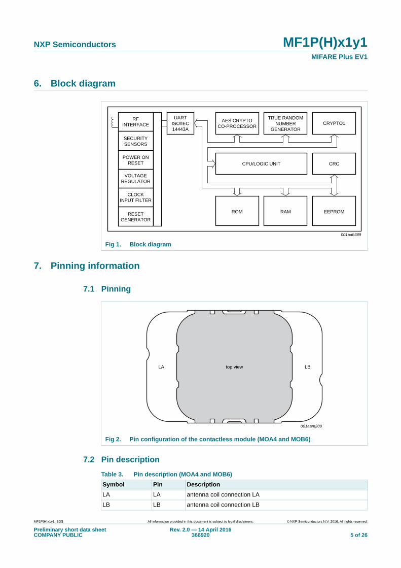
6. Block diagram
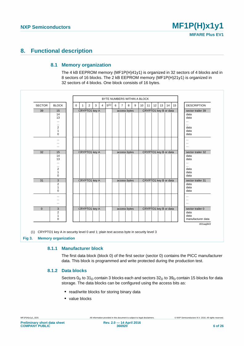
7. Pinning information
7.1 Pinning
7.2 Pin description
Fig 1. Block diagram
001aah389
RFINTERFACE
UARTISO/IEC14443A
AES CRYPTOCO-PROCESSOR
CPU/LOGIC UNIT CRC
EEPROMRAMROM
TRUE RANDOMNUMBER
GENERATORCRYPTO1
SECURITYSENSORS
POWER ONRESET
VOLTAGEREGULATOR
CLOCKINPUT FILTER
RESETGENERATOR
Fig 2. Pin configuration of the contactless module (MOA4 and MOB6)
001aam200
top viewLA LB
Table 3. Pin description (MOA4 and MOB6)
Symbol Pin Description
LA LA antenna coil connection LA
LB LB antenna coil connection LB
MF1P(H)x1y1_SDS All information provided in this document is subject to legal disclaimers. © NXP Semiconductors N.V. 2016. All rights reserved.
Preliminary short data sheetCOMPANY PUBLIC
Rev. 2.0 — 14 April 2016366920 5 of 26
NXP Semiconductors MF1P(H)x1y1MIFARE Plus EV1
8. Functional description
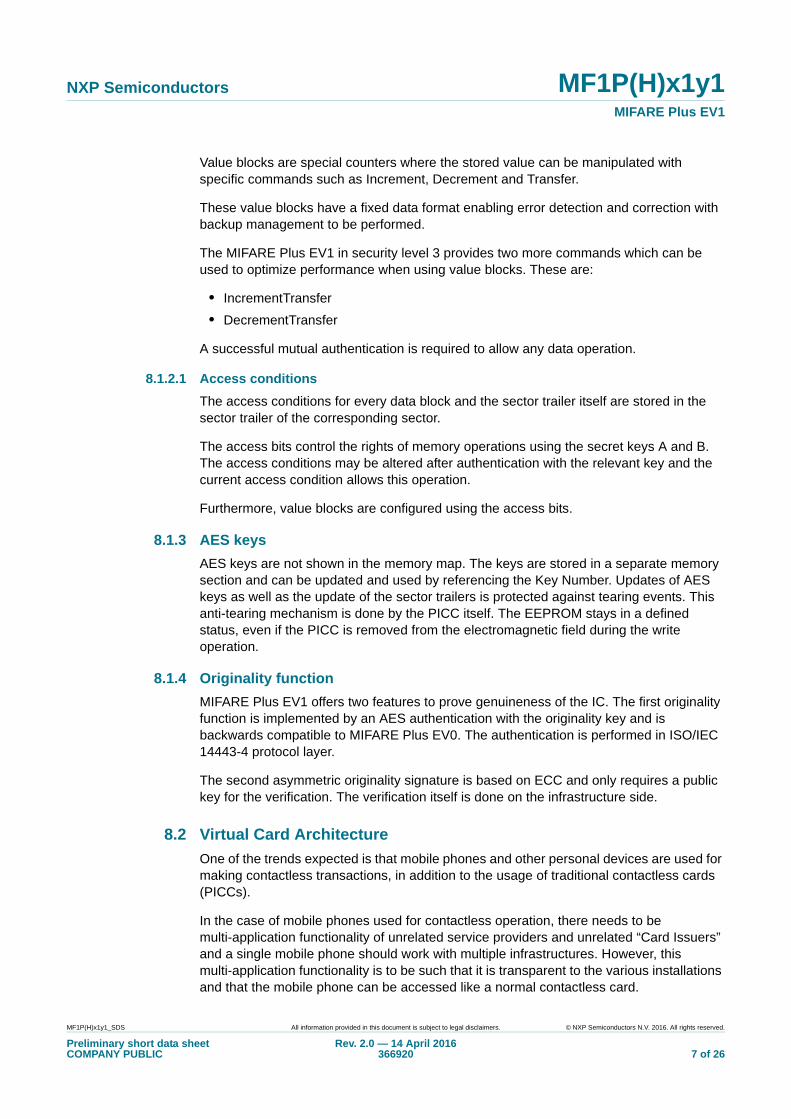
8.1 Memory organization
The 4 kB EEPROM memory (MF1P(H)41y1) is organized in 32 sectors of 4 blocks and in 8 sectors of 16 blocks. The 2 kB EEPROM memory (MF1P(H)21y1) is organized in 32 sectors of 4 blocks. One block consists of 16 bytes.
8.1.1 Manufacturer block
The first data block (block 0) of the first sector (sector 0) contains the PICC manufacturer data. This block is programmed and write protected during the production test.
8.1.2 Data blocks
Sectors 0D to 31D contain 3 blocks each and sectors 32D to 39D contain 15 blocks for data storage. The data blocks can be configured using the access bits as:
• read/write blocks for storing binary data
• value blocks
(1) CRYPTO1 key A in security level 0 and 1; plain text access byte in security level 3
Fig 3. Memory organization
001aaj843
SECTOR BLOCK DESCRIPTION0
39
32
31
0
15 CRYPTO1 key A access bytes
BYTE NUMBERS WITHIN A BLOCK
CRYPTO1 key B or data
CRYPTO1 key A access bytes CRYPTO1 key B or data
CRYPTO1 key A access bytes CRYPTO1 key B or data
CRYPTO1 key A access bytes CRYPTO1 key B or data
1413......210
151413......210
...
3
...
...
...
...
...
210
321
sector trailer 39datadata......datadatadata
sector trailer 32datadata......datadatadata
...
sector trailer 31
...
...
...
...
...
datadatadata
sector trailer 0datadatamanufacturer data0
1 2 3 4 5(1) 6 7 8 9 10 11 12 13 14 15
MF1P(H)x1y1_SDS All information provided in this document is subject to legal disclaimers. © NXP Semiconductors N.V. 2016. All rights reserved.
Preliminary short data sheetCOMPANY PUBLIC
Rev. 2.0 — 14 April 2016366920 6 of 26
NXP Semiconductors MF1P(H)x1y1MIFARE Plus EV1
Value blocks are special counters where the stored value can be manipulated with specific commands such as Increment, Decrement and Transfer.
These value blocks have a fixed data format enabling error detection and correction with backup management to be performed.
The MIFARE Plus EV1 in security level 3 provides two more commands which can be used to optimize performance when using value blocks. These are:
• IncrementTransfer
• DecrementTransfer
A successful mutual authentication is required to allow any data operation.
8.1.2.1 Access conditions
The access conditions for every data block and the sector trailer itself are stored in the sector trailer of the corresponding sector.
The access bits control the rights of memory operations using the secret keys A and B. The access conditions may be altered after authentication with the relevant key and the current access condition allows this operation.
Furthermore, value blocks are configured using the access bits.
8.1.3 AES keys
AES keys are not shown in the memory map. The keys are stored in a separate memory section and can be updated and used by referencing the Key Number. Updates of AES keys as well as the update of the sector trailers is protected against tearing events. This anti-tearing mechanism is done by the PICC itself. The EEPROM stays in a defined status, even if the PICC is removed from the electromagnetic field during the write operation.
8.1.4 Originality function
MIFARE Plus EV1 offers two features to prove genuineness of the IC. The first originality function is implemented by an AES authentication with the originality key and is backwards compatible to MIFARE Plus EV0. The authentication is performed in ISO/IEC 14443-4 protocol layer.
The second asymmetric originality signature is based on ECC and only requires a public key for the verification. The verification itself is done on the infrastructure side.
8.2 Virtual Card Architecture
One of the trends expected is that mobile phones and other personal devices are used for making contactless transactions, in addition to the usage of traditional contactless cards (PICCs).
In the case of mobile phones used for contactless operation, there needs to be multi-application functionality of unrelated service providers and unrelated “Card Issuers” and a single mobile phone should work with multiple infrastructures. However, this multi-application functionality is to be such that it is transparent to the various installations and that the mobile phone can be accessed like a normal contactless card.
MF1P(H)x1y1_SDS All information provided in this document is subject to legal disclaimers. © NXP Semiconductors N.V. 2016. All rights reserved.
Preliminary short data sheetCOMPANY PUBLIC
Rev. 2.0 — 14 April 2016366920 7 of 26
NXP Semiconductors MF1P(H)x1y1MIFARE Plus EV1
With the implemented Virtual Cards (VCs) concept, a Proximity Device (PD), e.g. the Secure Element in a mobile phone, can hold multiple VCs. With having multiple VCs in a single device there are several requirements:
1. It must be determined how the appropriate VC to use gets selected, in other words how a specific VC is to be presented at a given moment.
2. Privacy considerations need to be maintained. When a device can be freely interrogated about its UID, VC specific information (like implementation, file layout, ...) or even only to what installations the supported VCs belong, this data or the combination of a subset of it would make it possible to track a person from location to location. Furthermore, the combination of VCs could reveal a category of persons.
3. Performance and ease of use. The selection of the appropriate VC must be done fast, in order to increase transaction times only minimally.
4. Compliancy and portability to existing Card OSes supporting application selection methods on secure chip technologies, as defined by Java Card and GlobalPlatform.
The Virtual Card Architecture as implemented on the MF1P(H)x1y1 has the following benefits:
• Fast VC selection is possible by issuing a single ISOSelect command as defined by ISO/IEC 7816-4
• If Random ID is used, the UID can be retrieved in a very fast and secure way from the VC using ISOSelect and ISOExternalAuthenticate
• Detect whether a VC belongs to certain installation and do so fast and privacy friendly
• Proximity Check may also be enforced via a configuration, giving additionally protection against relay attacks
• Exchange capabilities, e.g. a key-set version indication together with the fast retrieval of the UID.
8.3 Proximity check
The Proximity Check is used in conjunction with the Virtual Card Architecture, see Section 8.2. It can also be used afterwards. It allows the PCD to verify whether the PICC is within a certain physical proximity.
MF1P(H)x1y1 enables ISO/IEC 7816-4 compliant Proximity Check by supporting wrapping of the native Proximity Check commands into ISO/IEC 7816-4 compliant APDUs, as outlined in Section 8.6.3.
The SL3 and SL1 after ISO/IEC 14443-4 activation offers the Proximity Check function which protect the PICC from relay attacks by measurement of the round trip time of a challenge-response interaction. If an attacker wants to mount a relay attack, then he necessarily introduces delays. Depending on how large the delays are, they may be detected. The accuracy of the time measurement and the residual relay attack window that remains is dependent on the intrinsic latency of the PICC as well as of the implementation of the reader.
MF1P(H)x1y1_SDS All information provided in this document is subject to legal disclaimers. © NXP Semiconductors N.V. 2016. All rights reserved.
Preliminary short data sheetCOMPANY PUBLIC
Rev. 2.0 — 14 April 2016366920 8 of 26
NXP Semiconductors MF1P(H)x1y1MIFARE Plus EV1
8.4 AES Secure Messaging
8.4.1 AES security concept
A MIFARE Plus transaction includes a set of operations from card activation, authentication to the reading and changing of data on the card. Each interaction with data on the card requires an authentication with the appropriate sector key. The result of such an authentication is called a session.
MIFARE Plus EV1 supports two secure messaging modes:
• EV0 secure messaging, which is fully backwards compatible with MIFARE Plus EV0.
• EV1 secure messaging.
The PCD can decide which mode to use.
8.4.2 Multi-sector authentication
This feature is available in security level 3 for data which is spread over multiple sectors to improve transaction performance.
Providing that such sectors are secured with identical keys (key value and key type) only a single authentication is required to read and/or write data from these sectors. There is no need to re-authenticate when accessing any data within these sectors. Therefore it is possible to configure a card in such a way that operating with only one authentication is needed in security level 3 to access all sectors.
8.5 Transaction MAC
The Transaction MAC feature helps preventing fraudulent merchant attacks. In example, it allows a merchant operating a point-of-sale terminal to prove that the transactions he executed with customers are genuine towards the back-end system. This is done by letting the card generate a Transaction MAC over the transaction with a key shared only by the card and the back-end system. The Transaction MAC feature can be activated block by block. Note that the pre-personalization of the card has to be done by the card issuer and not by the merchants provider.
MAC generation also involves a Transaction MAC Counter maintained by the card, which allows the back-end system to detect replay attempts by the merchant. In addition, this counter allows the back-end system to detect missing transactions, which in turn allows detecting fraud where in example the merchant has increased the balance without reporting the transaction. Note that a counter also allows for easier detection mechanisms of replay than keeping logs with fingerprints of every transaction.
As only fraud detection might not be sufficient if one cannot point to the fraudulent merchant, an additional configuration option allows the back-end to require that the merchant’s terminal commits its identity, called ReaderID, during the transaction. This requires support of a SAM which allows secure commit of its UID.
The card supports linking ReaderIDs of merchants by storing the committed ReaderID and returning the ReaderID of the previous transaction. This way the back-end system can detect which merchant did not report missing transactions.
MF1P(H)x1y1_SDS All information provided in this document is subject to legal disclaimers. © NXP Semiconductors N.V. 2016. All rights reserved.
Preliminary short data sheetCOMPANY PUBLIC
Rev. 2.0 — 14 April 2016366920 9 of 26
NXP Semiconductors MF1P(H)x1y1MIFARE Plus EV1
8.6 Card activation and communication protocol
The ISO/IEC 14443-3 anticollision mechanism allows for simultaneous handling of multiple PICCs in the field. The anticollision algorithm selects each PICC individually and ensures that execution of a transaction with a selected PICC is performed correctly without data corruption from other PICCs in the field.
There are two different versions of the PICC. The UID is programmed into a locked part of the NV-memory reserved for the manufacturer:
• unique 7-byte serial number
• non-unique 4-byte serial number
Due to security and system requirements, these bytes are write-protected after being programmed by the PICC manufacturer at production time.
Remark: The programmed 4-byte NUID serial number is not globally unique which has to be considered in the contactless system design. See Ref. 14 for further information regarding handling of UIDs.
The customer must decide which UID length to use when ordering the product, see Table 2 for ordering information.
A MF1P(H)x1y1 with 7-byte UID supports the additional UID configuration options as defined in Ref. 3 using the MF_PersonalizeUIDUsage command after ISO/IEC 14443-3 activation. Note that the MF_PersonalizeUIDUsage command can only be sent once.
During personalization, the PICC can be configured to support Random ID. The user can configure whether Random ID or fixed UID shall be used. According to ISO/IEC 14443-3 the first anticollision loop (see Ref. 7) returns the Random Number Tag 08h, the 3-byte Random Number and the BCC, if Random ID is used. In case Random ID is configured, the real UID can be retrieved using the ISOSelect and ISOExternalAuthenticate commands or by reading out block 0 of sector 0.
8.6.1 Backwards compatibility protocol
The backwards compatibility of this product, as used in security level 1, runs on the same protocol layer as MIFARE Classic EV1 1K and MIFARE Classic EV1 4K. The protocol consists of the following components:
• Frame definition: according to ISO/IEC 14443-3
• Bit encoding: according to ISO/IEC 14443-2
• Error code handling: handling is proprietary as error codes are formatted in half bytes.
• Command specification: commands are proprietary. Please use the specification as in Ref. 3 and Ref. 4 and the additional commands which are only implemented in MIFARE Plus EV1 as described in this document and in Ref. 1.
The following security levels can run on this protocol:
• Security Level 0
• Security Level 1
MF1P(H)x1y1_SDS All information provided in this document is subject to legal disclaimers. © NXP Semiconductors N.V. 2016. All rights reserved.
Preliminary short data sheetCOMPANY PUBLIC
Rev. 2.0 — 14 April 2016366920 10 of 26
NXP Semiconductors MF1P(H)x1y1MIFARE Plus EV1
8.6.2 ISO/IEC 14443-4 Protocol
The ISO/IEC 14443-4 Protocol (also known as T=CL) is used in many processor cards. This protocol is used for the MIFARE Plus EV1 with the following security levels:
• Security Level 0: all commands
• Security Level 1: for the sector or card level SL switch, the AES originality function, AES Key update, configuration data update, GetVersion and Read_Sig
• Security Level 3: all commands
Remark: The ISO/IEC 14443-4 protocol is also used to operate any sector that has been switched to SL3 or when operating a sector using SL3 commands which has been switched to SL1SL3Mix mode.
8.6.3 ISO/IEC 7816-4 Protocol
MIFARE Plus EV1 supports the APDU message structure according to ISO/IEC 7816-4 for
• an optional wrapping of the native APDU format
• for the additionally implemented standard ISO/IEC 7816-4 commands for Virtual Card
selection
8.7 Security level switching
The MIFARE Plus EV1 offers a unique feature to support migration from CRYPTO1 based systems to AES based operation. The migration on the card-side is done using different security levels supporting different cryptographic algorithms and protocols. There are three security levels:
• Security level 0: initial delivery configuration, used for card personalization
• Security level 1: 3-Pass CRYPTO1 Authentication (backwards compatibility mode with MIFARE Classic EV1 1K and MIFARE Classic EV1 4K) with optional AES authentication, optional 3-Pass AES Authentication and secure messaging.
• Security level 3: 3-Pass authentication based on AES, new data manipulation commands secured by AES encryption and an AES based MACing method
The security level switching (i.e. from security level 1 to security level 3) is performed using the dedicated AES authentication switching keys.
Security level switching can be done for the whole card (CardSecurityLevel) or for dedicated sectors only (SectorSecurityLevel). In case of dedicated sectors, these can also be switched to a mixed mode SL1SL3Mix, where both security level 1 and security level 3 operations are accepted. Security level switching, both at card or at sector level, is only possible to a higher security level and not to a lower security level.
MF1P(H)x1y1_SDS All information provided in this document is subject to legal disclaimers. © NXP Semiconductors N.V. 2016. All rights reserved.
Preliminary short data sheetCOMPANY PUBLIC
Rev. 2.0 — 14 April 2016366920 11 of 26
NXP Semiconductors MF1P(H)x1y1MIFARE Plus EV1
8.7.1 Switching CardSecurityLevel
CardSecurityLevel switching of MF1P(H)x1y1 means that the whole PICC is switching its security level at once. This is also the method available in MIFARE Plus EV0 and is done by an AES authentication with the L3SwitchKey.
The product is delivered in SL0. It is possible to upgrade the PICC to security level 3 either passing through the security level 1 or directly from security level 0.
8.7.2 Switching SectorSecurityLevel
Switching the Security Level of dedicated MIFARE Sectors is done by a multiple key AES authentication, called AuthenticateSectorSwitch, addressing the L3SectorSwitchKey or L1L3MixSectorSwitchKey, and the AESSectorKeyB of the targeted sectors. This command is only available after ISO/IEC 14443-4 activation in security level 1.
8.8 Security level 0
Security level 0 is the initial delivery configuration of the PICC. The card can be operated either using the backwards compatibility protocol or the ISO/IEC 14443-4 protocol.
In this level, the card can be personalized including the programming of user data as well as CRYPTO1 and/or AES keys. In addition, the originality function can be used.
The following mandatory AES keys must be written, using the WritePerso command before the PICC can be switched to security level 1 or security level 3.
Security level switching is performed using the CommitPerso command:
• CardConfigurationKey
• CardMasterKey
• L3SwitchKey
When the pre-personalization of the PICC is finished it is possible to upgrade the PICC from security level 0 either to security level 1 or directly to security level 3 with CommitPerso command.
Using the originality function, it is possible to verify that the chip is a genuine NXP Semiconductors MIFARE Plus.
MF1P(H)x1y1_SDS All information provided in this document is subject to legal disclaimers. © NXP Semiconductors N.V. 2016. All rights reserved.
Preliminary short data sheetCOMPANY PUBLIC
Rev. 2.0 — 14 April 2016366920 12 of 26
NXP Semiconductors MF1P(H)x1y1MIFARE Plus EV1
8.9 Security level 1
Security level 1 offers the same functionality as a MIFARE Classic EV1 1K andMIFARE Classic EV1 4K using the backwards compatibility protocol, see Ref. 3 and Ref. 4.
Furthermore, an optional AES authentication is available in this level without affecting the MIFARE Classic EV1 1K and MIFARE Classic EV1 4K functionality. The authenticity of the card can be proven using strong cryptographic means with this additional functionality.
Response timings may differ from the MIFARE Classic EV1 1K/4K products.
In addition to the backwards compatibility mode, after a successful ISO/IEC 14443-4 activation the originality function can be executed or the CardSecurityLevel or SectorSecurityLevel switched to higher security levels. In addition to those features already available in MIFARE Plus EV0, MIFARE Plus EV1 offers the possibility to update AESSectorKeys and VCSystemData.
MIFARE Plus EV1 can be operated like MIFARE Plus EV0 in SL1 which means that all memory operations on each sector are requiring legacy MIFARE Classic EV1 commands using CRYPTO1 enciphering. Beyond that, MIFARE Plus EV1 offers the flexibility to either switch distinct sectors to SL3 and operate them in AES secure messaging or enable SL1SL3MixMode on distinct sectors. Sectors in SL1SL3MixMode can be operated either using the backwards compatible MIFARE Classic EV1 commands when activated to ISO/IEC 14443-3 or using AES secure messaging when activated to ISO/IEC 14443-4. In example, this enables end-to-end communication to a MIFARE Plus EV1 using a secure AES channel while leaving the operation in the application on MIFARE Classic EV1 commands for a migration period.
Also, the Transaction MAC feature is available in security level 1 after ISO/IEC14443-3 activation. The Transaction MAC processing in security level 1 of the Authentication, Read, Write, Increment, Decrement, Transfer and Restore commands is the same as their security level 3 equivalents with a few differences, as described later and in Ref. 1. The CommitReaderID command is not supported.
Using the originality function it is possible to verify if the chip is a genuine NXP Semiconductors MIFARE Plus EV1.
MF1P(H)x1y1_SDS All information provided in this document is subject to legal disclaimers. © NXP Semiconductors N.V. 2016. All rights reserved.
Preliminary short data sheetCOMPANY PUBLIC
Rev. 2.0 — 14 April 2016366920 13 of 26
NXP Semiconductors MF1P(H)x1y1MIFARE Plus EV1
8.10 Security level 3
The operation in security level 3 is solely based on the ISO/IEC 14443-4 protocol layer. The usage of the backwards compatibility protocol is not possible.
In security level 3, a mandatory AES authentication between PICC and reader is conducted, where two keys are generated as a function of the random numbers from the PICC and the reader as well as of the shared key.
These two session keys are used to secure the data which is exchanged on the interface between the card and reader. One of the two keys is used to ensure the confidentiality of the command and the response while the other key ensures the integrity of the command and the response.
MIFARE Plus EV1 features the secure messaging from its predecessor MIFARE Plus EV0 and it offers the possibility to choose the newly introduced EV1 secure messaging. On First Authenticate, the PCD can use the PCD capability bytes to chose between MIFARE Plus EV0 and MIFARE Plus EV1 secure messaging.
The reader can decide which security needs to be used in the communication between PICC and reader. In the simplest case, all commands are secured by a MAC, such that the PICC will only accept commands from the authenticated reader. Any message tampering is detected by verifying the MAC. All responses are appended by a MAC to prove to the reader that neither the command nor the response have been compromised.
If performance is the highest priority, the card can be configured to omit the MAC for read commands. The card then accepts read commands without knowing whether they are authentic. However, there is a mechanism to prove to the reader that the read response is resulting from the unmodified read command that it sent.
Other commands, like write commands, always need to have a MAC appended to ensure that no memory changes are carried out without proving the authenticity of the command.
The reader can decide for each command whether a MAC is included in the response. When the appropriate MAC is received, due to linked MACs the reader knows that the command and commands before it were properly executed.
All commands between two consecutive First Authenticate commands belong to one transaction and the MACing mechanism assures integrity of the whole transaction.
If the MAC on read responses is omitted, the integrity of all read responses within one session can still be verified by including a MAC on one read response before issuing the next First or Following Authenticate command.
To balance performance and confidentiality of the transaction, each data block in a sector can be configured to allow or disallow sending/receiving plain data.
MF1P(H)x1y1_SDS All information provided in this document is subject to legal disclaimers. © NXP Semiconductors N.V. 2016. All rights reserved.
Preliminary short data sheetCOMPANY PUBLIC
Rev. 2.0 — 14 April 2016366920 14 of 26
NXP Semiconductors MF1P(H)x1y1MIFARE Plus EV1
9. Look-up tables
9.1 Security level 0, 1, 2, 3: ISO/IEC 14443-3
9.2 Security level 0, 1, 2, 3: ISO/IEC 14443-4
Please find more information on ISO/IEC 14443-3 in Ref. 7 as well as on the settings of ATQA, SAK and ATS in Ref. 6.
9.3 SL0 command overview
Table 4. ISO/IEC 14443-3
Command Description
REQA the REQA and ATQA commands are fully implemented according to ISO/IEC 14443-3
WUPA the WAKE-UP command is fully implemented according to ISO/IEC 14443-3
ANTICOLLISION/SELECT cascade level 1
the ANTICOLLISION and SELECT commands are fully implemented according to ISO/IEC 14443-3. The response is part 1 of the UID.
ANTICOLLISION/SELECT cascade level 2 for 7 byte UID version
the ANTICOLLISION and SELECT commands are fully implemented according to ISO/IEC 14443-3. The response is part 2 of the UID.
HALT the HALT command is fully implemented according to ISO/IEC 14443-3
Table 5. ISO/IEC 14443-4
Command Description
RATS the response to the RATS command identifies the PICC type to the PCD.
PPS the PPS command allows individual selection of the communication baud rate between PCD and PICC. It is possible for MF1PLUSx0 to individually set the communication baud rate independently for both directions.
DESELECT deselection according to ISO/IEC 14443-4.
Table 6. SL0 command overview
Command Description
Commands available after ISO/IEC 14443-3 activation
Read_Sig Retrieve the ECC originality check signature.
WritePerso pre Personalization of AES Keys and all blocks
CommitPerso switch to SL1 or SL3
AuthenticateFirst (part 1) first authenticate
AuthenticateNonFirst (part 1) following authenticate
AuthenticateContinue (part 2) second authentication step
VCSupportLastISOL3 check if the Virtual Card Concept is supported, communicate PCD capabilities and retrieve the UID
Commands available after ISO/IEC 14443-4 activation
GetVersion returns manufacturing related data of the PICC
MF1P(H)x1y1_SDS All information provided in this document is subject to legal disclaimers. © NXP Semiconductors N.V. 2016. All rights reserved.
Preliminary short data sheetCOMPANY PUBLIC
Rev. 2.0 — 14 April 2016366920 15 of 26
NXP Semiconductors MF1P(H)x1y1MIFARE Plus EV1
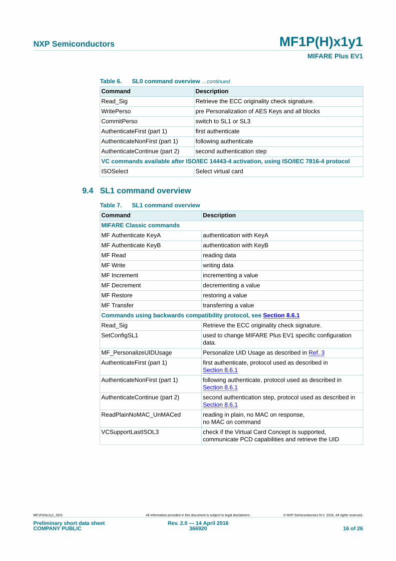
9.4 SL1 command overview
Read_Sig Retrieve the ECC originality check signature.
WritePerso pre Personalization of AES Keys and all blocks
CommitPerso switch to SL1 or SL3
AuthenticateFirst (part 1) first authenticate
AuthenticateNonFirst (part 1) following authenticate
AuthenticateContinue (part 2) second authentication step
VC commands available after ISO/IEC 14443-4 activation, using ISO/IEC 7816-4 protocol
ISOSelect Select virtual card
Table 6. SL0 command overview …continued
Command Description
Table 7. SL1 command overview
Command Description
MIFARE Classic commands
MF Authenticate KeyA authentication with KeyA
MF Authenticate KeyB authentication with KeyB
MF Read reading data
MF Write writing data
MF Increment incrementing a value
MF Decrement decrementing a value
MF Restore restoring a value
MF Transfer transferring a value
Commands using backwards compatibility protocol, see Section 8.6.1
Read_Sig Retrieve the ECC originality check signature.
SetConfigSL1 used to change MIFARE Plus EV1 specific configuration data.
MF_PersonalizeUIDUsage Personalize UID Usage as described in Ref. 3
AuthenticateFirst (part 1) first authenticate, protocol used as described in Section 8.6.1
AuthenticateNonFirst (part 1) following authenticate, protocol used as described in Section 8.6.1
AuthenticateContinue (part 2) second authentication step, protocol used as described in Section 8.6.1
ReadPlainNoMAC_UnMACed reading in plain, no MAC on response, no MAC on command
VCSupportLastISOL3 check if the Virtual Card Concept is supported, communicate PCD capabilities and retrieve the UID
MF1P(H)x1y1_SDS All information provided in this document is subject to legal disclaimers. © NXP Semiconductors N.V. 2016. All rights reserved.
Preliminary short data sheetCOMPANY PUBLIC
Rev. 2.0 — 14 April 2016366920 16 of 26
NXP Semiconductors MF1P(H)x1y1MIFARE Plus EV1
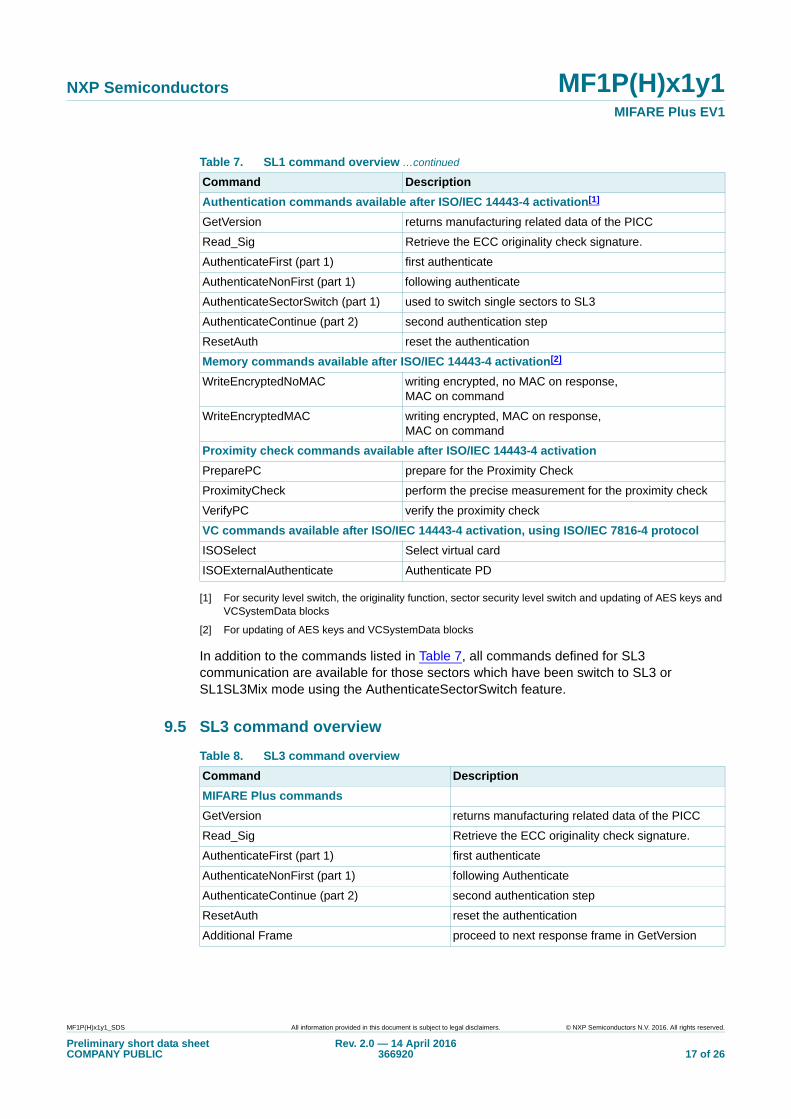
[1] For security level switch, the originality function, sector security level switch and updating of AES keys and VCSystemData blocks
[2] For updating of AES keys and VCSystemData blocks
In addition to the commands listed in Table 7, all commands defined for SL3 communication are available for those sectors which have been switch to SL3 or SL1SL3Mix mode using the AuthenticateSectorSwitch feature.
9.5 SL3 command overview
Authentication commands available after ISO/IEC 14443-4 activation[1]
GetVersion returns manufacturing related data of the PICC
Read_Sig Retrieve the ECC originality check signature.
AuthenticateFirst (part 1) first authenticate
AuthenticateNonFirst (part 1) following authenticate
AuthenticateSectorSwitch (part 1) used to switch single sectors to SL3
AuthenticateContinue (part 2) second authentication step
ResetAuth reset the authentication
Memory commands available after ISO/IEC 14443-4 activation[2]
WriteEncryptedNoMAC writing encrypted, no MAC on response, MAC on command
WriteEncryptedMAC writing encrypted, MAC on response, MAC on command
Proximity check commands available after ISO/IEC 14443-4 activation
PreparePC prepare for the Proximity Check
ProximityCheck perform the precise measurement for the proximity check
VerifyPC verify the proximity check
VC commands available after ISO/IEC 14443-4 activation, using ISO/IEC 7816-4 protocol
ISOSelect Select virtual card
ISOExternalAuthenticate Authenticate PD
Table 7. SL1 command overview …continued
Command Description
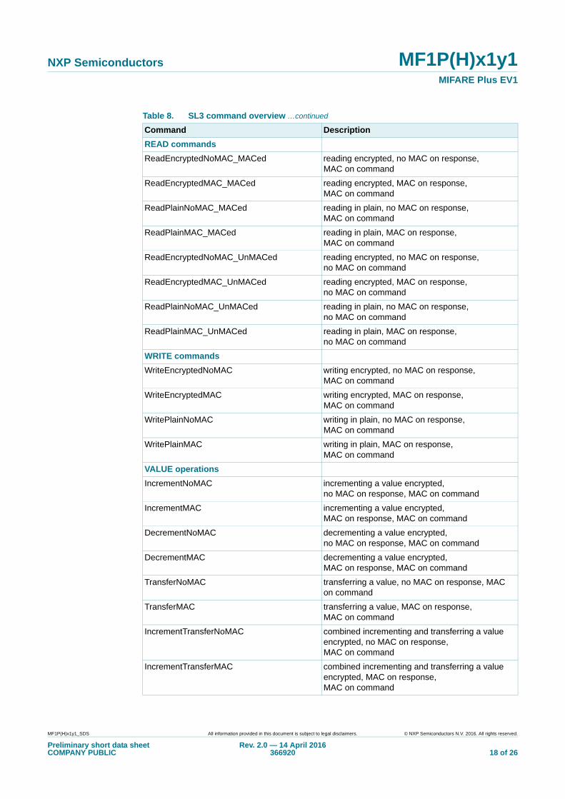
Table 8. SL3 command overview
Command Description
MIFARE Plus commands
GetVersion returns manufacturing related data of the PICC
Read_Sig Retrieve the ECC originality check signature.
AuthenticateFirst (part 1) first authenticate
AuthenticateNonFirst (part 1) following Authenticate
AuthenticateContinue (part 2) second authentication step
ResetAuth reset the authentication
Additional Frame proceed to next response frame in GetVersion
MF1P(H)x1y1_SDS All information provided in this document is subject to legal disclaimers. © NXP Semiconductors N.V. 2016. All rights reserved.
Preliminary short data sheetCOMPANY PUBLIC
Rev. 2.0 — 14 April 2016366920 17 of 26
NXP Semiconductors MF1P(H)x1y1MIFARE Plus EV1
READ commands
ReadEncryptedNoMAC_MACed reading encrypted, no MAC on response, MAC on command
ReadEncryptedMAC_MACed reading encrypted, MAC on response, MAC on command
ReadPlainNoMAC_MACed reading in plain, no MAC on response, MAC on command
ReadPlainMAC_MACed reading in plain, MAC on response, MAC on command
ReadEncryptedNoMAC_UnMACed reading encrypted, no MAC on response, no MAC on command
ReadEncryptedMAC_UnMACed reading encrypted, MAC on response, no MAC on command
ReadPlainNoMAC_UnMACed reading in plain, no MAC on response, no MAC on command
ReadPlainMAC_UnMACed reading in plain, MAC on response, no MAC on command
WRITE commands
WriteEncryptedNoMAC writing encrypted, no MAC on response, MAC on command
WriteEncryptedMAC writing encrypted, MAC on response, MAC on command
WritePlainNoMAC writing in plain, no MAC on response, MAC on command
WritePlainMAC writing in plain, MAC on response, MAC on command
VALUE operations
IncrementNoMAC incrementing a value encrypted, no MAC on response, MAC on command
IncrementMAC incrementing a value encrypted, MAC on response, MAC on command
DecrementNoMAC decrementing a value encrypted, no MAC on response, MAC on command
DecrementMAC decrementing a value encrypted, MAC on response, MAC on command
TransferNoMAC transferring a value, no MAC on response, MAC on command
TransferMAC transferring a value, MAC on response, MAC on command
IncrementTransferNoMAC combined incrementing and transferring a value encrypted, no MAC on response, MAC on command
IncrementTransferMAC combined incrementing and transferring a value encrypted, MAC on response, MAC on command
Table 8. SL3 command overview …continued
Command Description
MF1P(H)x1y1_SDS All information provided in this document is subject to legal disclaimers. © NXP Semiconductors N.V. 2016. All rights reserved.
Preliminary short data sheetCOMPANY PUBLIC
Rev. 2.0 — 14 April 2016366920 18 of 26
NXP Semiconductors MF1P(H)x1y1MIFARE Plus EV1
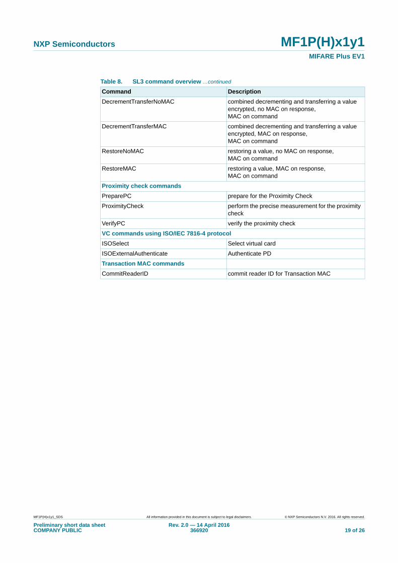
DecrementTransferNoMAC combined decrementing and transferring a value encrypted, no MAC on response, MAC on command
DecrementTransferMAC combined decrementing and transferring a value encrypted, MAC on response, MAC on command
RestoreNoMAC restoring a value, no MAC on response, MAC on command
RestoreMAC restoring a value, MAC on response, MAC on command
Proximity check commands
PreparePC prepare for the Proximity Check
ProximityCheck perform the precise measurement for the proximity check
VerifyPC verify the proximity check
VC commands using ISO/IEC 7816-4 protocol
ISOSelect Select virtual card
ISOExternalAuthenticate Authenticate PD
Transaction MAC commands
CommitReaderID commit reader ID for Transaction MAC
Table 8. SL3 command overview …continued
Command Description
MF1P(H)x1y1_SDS All information provided in this document is subject to legal disclaimers. © NXP Semiconductors N.V. 2016. All rights reserved.
Preliminary short data sheetCOMPANY PUBLIC
Rev. 2.0 — 14 April 2016366920 19 of 26
NXP Semiconductors MF1P(H)x1y1MIFARE Plus EV1
10. Limiting values
Stresses above one or more of the limiting values may cause permanent damage to the device. Exposure to limiting values for extended periods may affect device reliability.
[1] ANSI/ESDA/JEDEC JS-001; Human body model: C = 100 pF, R = 1.5 k
Table 9. Limiting valuesIn accordance with the Absolute Maximum Rating System (IEC 60134).
Symbol Parameter Min Max Unit
II input current - 50 mA
Ptot/pack total power dissipation per package - 200 mW
Tstg storage temperature 55 125 C
Tamb ambient temperature 25 70 C
VESD electrostatic discharge voltage on LA/LB [1] - 2 kV
MF1P(H)x1y1_SDS All information provided in this document is subject to legal disclaimers. © NXP Semiconductors N.V. 2016. All rights reserved.
Preliminary short data sheetCOMPANY PUBLIC
Rev. 2.0 — 14 April 2016366920 20 of 26
NXP Semiconductors MF1P(H)x1y1MIFARE Plus EV1
11. Abbreviations
Table 10. Abbreviations
Acronym Description
AES Advanced Encryption Standard
APDU Application Protocol Data Unit
ATQA Answer To reQuest
ATS Answer To Select
BCC Bit Count Check
EEPROM Electrically Erasable Programmable Read-Only Memory
LCR L = inductance, Capacitance, Resistance (LCR meter)
MAC Message Authentication Code
NUID Non-Unique IDentifier
NV Non-Volatile memory
PCD Proximity Coupling Device (Contactless Reader)
PICC Proximity Integrated Circuit Card (Contactless Card)
PPS Protocol Parameter Selection
RATS Request Answer To Select
REQA REQuest Answer
SAK Select AcKnowledge, type A
SECS-II SEMI Equipment Communications Standard part 2
SEMI Semiconductors Equipment and Materials International
SL Security level
UID Unique IDentifier
VC Virtual Card, one MIFARE Plus PICC is one virtual card
WUPA Wake Up Protocol A
MF1P(H)x1y1_SDS All information provided in this document is subject to legal disclaimers. © NXP Semiconductors N.V. 2016. All rights reserved.
Preliminary short data sheetCOMPANY PUBLIC
Rev. 2.0 — 14 April 2016366920 21 of 26
NXP Semiconductors MF1P(H)x1y1MIFARE Plus EV1
12. References
[1] MIFARE Plus EV1 — Data sheet, Doc. No. 3226**2
[2] MF1P(H)x1y1 Wafer specification — Data sheet addendum, Doc. No. 3441**
[3] MIFARE Classic EV1 1K — Data sheet, Doc. No. 2792**
[4] MIFARE Classic EV1 4K — Data sheet, Doc. No. 2794**
[5] AN10787 MIFARE Application Directory (MAD) — Application note, Doc. No. 0018**
[6] MIFARE Type identification procedure — Application note, Doc. No. 1843**
[7] ISO/IEC 14443 PICC selection — Application note, Doc. No. 1308**
[8] ISO/IEC 7816-4:2005 — Identification cards – Integrated circuit cards – Part 4: Organization, security and commands for interchange. January 2005.
[9] NIST Special Publication 800-38A — Recommendation for block cipher modes of operation: methods and techniques, 2001.
[10] NIST Special Publication 800-38B — Recommendation for block cipher modes of operation: The CMAC mode for authentication.
[11] ISO/IEC 14443 Standard — Identification cards - contactless integrated circuit cards - proximity cards.
[12] Recommendation for block cipher modes of operation: methods and techniques — FIPS PUB 197 ADVANCED ENCRYPTION STANDARD.
[13] ISO/IEC 9797-1 Standard — Information technology - security techniques - Message Authentication Codes (MACs) - Part 1: Mechanisms using a block cipher.
[14] MIFARE and handling of UIDs — Application note, Doc. No. 1907**
2. ** ... document version number
MF1P(H)x1y1_SDS All information provided in this document is subject to legal disclaimers. © NXP Semiconductors N.V. 2016. All rights reserved.
Preliminary short data sheetCOMPANY PUBLIC
Rev. 2.0 — 14 April 2016366920 22 of 26
NXP Semiconductors MF1P(H)x1y1MIFARE Plus EV1
13. Revision history
Table 11. Revision history
Document ID Release date Data sheet status Change notice Supersedes
MF1P(H)x1y1 v.2.0 20160414 Preliminary short data sheet - -
MF1P(H)x1y1_SDS All information provided in this document is subject to legal disclaimers. © NXP Semiconductors N.V. 2016. All rights reserved.
Preliminary short data sheetCOMPANY PUBLIC
Rev. 2.0 — 14 April 2016366920 23 of 26
NXP Semiconductors MF1P(H)x1y1MIFARE Plus EV1
14. Legal information
14.1 Data sheet status
[1] Please consult the most recently issued document before initiating or completing a design.
[2] The term ‘short data sheet’ is explained in section “Definitions”.
[3] The product status of device(s) described in this document may have changed since this document was published and may differ in case of multiple devices. The latest product status information is available on the Internet at URL http://www.nxp.com.
14.2 Definitions
Draft — The document is a draft version only. The content is still under internal review and subject to formal approval, which may result in modifications or additions. NXP Semiconductors does not give any representations or warranties as to the accuracy or completeness of information included herein and shall have no liability for the consequences of use of such information.
Short data sheet — A short data sheet is an extract from a full data sheet with the same product type number(s) and title. A short data sheet is intended for quick reference only and should not be relied upon to contain detailed and full information. For detailed and full information see the relevant full data sheet, which is available on request via the local NXP Semiconductors sales office. In case of any inconsistency or conflict with the short data sheet, the full data sheet shall prevail.
Product specification — The information and data provided in a Product data sheet shall define the specification of the product as agreed between NXP Semiconductors and its customer, unless NXP Semiconductors and customer have explicitly agreed otherwise in writing. In no event however, shall an agreement be valid in which the NXP Semiconductors product is deemed to offer functions and qualities beyond those described in the Product data sheet.
14.3 Disclaimers
Limited warranty and liability — Information in this document is believed to be accurate and reliable. However, NXP Semiconductors does not give any representations or warranties, expressed or implied, as to the accuracy or completeness of such information and shall have no liability for the consequences of use of such information. NXP Semiconductors takes no responsibility for the content in this document if provided by an information source outside of NXP Semiconductors.
In no event shall NXP Semiconductors be liable for any indirect, incidental, punitive, special or consequential damages (including - without limitation - lost profits, lost savings, business interruption, costs related to the removal or replacement of any products or rework charges) whether or not such damages are based on tort (including negligence), warranty, breach of contract or any other legal theory.
Notwithstanding any damages that customer might incur for any reason whatsoever, NXP Semiconductors’ aggregate and cumulative liability towards customer for the products described herein shall be limited in accordance with the Terms and conditions of commercial sale of NXP Semiconductors.
Right to make changes — NXP Semiconductors reserves the right to make changes to information published in this document, including without limitation specifications and product descriptions, at any time and without notice. This document supersedes and replaces all information supplied prior to the publication hereof.
Suitability for use — NXP Semiconductors products are not designed, authorized or warranted to be suitable for use in life support, life-critical or safety-critical systems or equipment, nor in applications where failure or malfunction of an NXP Semiconductors product can reasonably be expected to result in personal injury, death or severe property or environmental damage. NXP Semiconductors and its suppliers accept no liability for inclusion and/or use of NXP Semiconductors products in such equipment or applications and therefore such inclusion and/or use is at the customer’s own risk.
Applications — Applications that are described herein for any of these products are for illustrative purposes only. NXP Semiconductors makes no representation or warranty that such applications will be suitable for the specified use without further testing or modification.
Customers are responsible for the design and operation of their applications and products using NXP Semiconductors products, and NXP Semiconductors accepts no liability for any assistance with applications or customer product design. It is customer’s sole responsibility to determine whether the NXP Semiconductors product is suitable and fit for the customer’s applications and products planned, as well as for the planned application and use of customer’s third party customer(s). Customers should provide appropriate design and operating safeguards to minimize the risks associated with their applications and products.
NXP Semiconductors does not accept any liability related to any default, damage, costs or problem which is based on any weakness or default in the customer’s applications or products, or the application or use by customer’s third party customer(s). Customer is responsible for doing all necessary testing for the customer’s applications and products using NXP Semiconductors products in order to avoid a default of the applications and the products or of the application or use by customer’s third party customer(s). NXP does not accept any liability in this respect.
Limiting values — Stress above one or more limiting values (as defined in the Absolute Maximum Ratings System of IEC 60134) will cause permanent damage to the device. Limiting values are stress ratings only and (proper) operation of the device at these or any other conditions above those given in the Recommended operating conditions section (if present) or the Characteristics sections of this document is not warranted. Constant or repeated exposure to limiting values will permanently and irreversibly affect the quality and reliability of the device.
Terms and conditions of commercial sale — NXP Semiconductors products are sold subject to the general terms and conditions of commercial sale, as published at http://www.nxp.com/profile/terms, unless otherwise agreed in a valid written individual agreement. In case an individual agreement is concluded only the terms and conditions of the respective agreement shall apply. NXP Semiconductors hereby expressly objects to applying the customer’s general terms and conditions with regard to the purchase of NXP Semiconductors products by customer.
No offer to sell or license — Nothing in this document may be interpreted or construed as an offer to sell products that is open for acceptance or the grant, conveyance or implication of any license under any copyrights, patents or other industrial or intellectual property rights.
Document status[1][2] Product status[3] Definition
Objective [short] data sheet Development This document contains data from the objective specification for product development.
Preliminary [short] data sheet Qualification This document contains data from the preliminary specification.
Product [short] data sheet Production This document contains the product specification.
MF1P(H)x1y1_SDS All information provided in this document is subject to legal disclaimers. © NXP Semiconductors N.V. 2016. All rights reserved.
Preliminary short data sheetCOMPANY PUBLIC
Rev. 2.0 — 14 April 2016366920 24 of 26
NXP Semiconductors MF1P(H)x1y1MIFARE Plus EV1
Export control — This document as well as the item(s) described herein may be subject to export control regulations. Export might require a prior authorization from competent authorities.
Quick reference data — The Quick reference data is an extract of the product data given in the Limiting values and Characteristics sections of this document, and as such is not complete, exhaustive or legally binding.
Non-automotive qualified products — Unless this data sheet expressly states that this specific NXP Semiconductors product is automotive qualified, the product is not suitable for automotive use. It is neither qualified nor tested in accordance with automotive testing or application requirements. NXP Semiconductors accepts no liability for inclusion and/or use of non-automotive qualified products in automotive equipment or applications.
In the event that customer uses the product for design-in and use in automotive applications to automotive specifications and standards, customer (a) shall use the product without NXP Semiconductors’ warranty of the product for such automotive applications, use and specifications, and (b) whenever customer uses the product for automotive applications beyond NXP Semiconductors’ specifications such use shall be solely at customer’s own risk, and (c) customer fully indemnifies NXP Semiconductors for any liability, damages or failed product claims resulting from customer design and use of the product for automotive applications beyond NXP Semiconductors’ standard warranty and NXP Semiconductors’ product specifications.
Translations — A non-English (translated) version of a document is for reference only. The English version shall prevail in case of any discrepancy between the translated and English versions.
14.4 Licenses
14.5 TrademarksNotice: All referenced brands, product names, service names and trademarks are the property of their respective owners.
MIFARE — is a trademark of NXP B.V.
MIFARE Classic — is a trademark of NXP B.V.
MIFARE Plus — is a trademark of NXP B.V.
15. Contact information
For more information, please visit: http://www.nxp.com
For sales office addresses, please send an email to: [email protected]
ICs with DPA Countermeasures functionality
NXP ICs containing functionality implementing countermeasures to Differential Power Analysis and Simple Power Analysis are produced and sold under applicable license from Cryptography Research, Inc.
MF1P(H)x1y1_SDS All information provided in this document is subject to legal disclaimers. © NXP Semiconductors N.V. 2016. All rights reserved.
Preliminary short data sheetCOMPANY PUBLIC
Rev. 2.0 — 14 April 2016366920 25 of 26
NXP Semiconductors MF1P(H)x1y1MIFARE Plus EV1
16. Contents
1 General description . . . . . . . . . . . . . . . . . . . . . . 1
2 Features and benefits . . . . . . . . . . . . . . . . . . . . 2
3 Applications . . . . . . . . . . . . . . . . . . . . . . . . . . . . 2
4 Quick reference data . . . . . . . . . . . . . . . . . . . . . 3
5 Ordering information. . . . . . . . . . . . . . . . . . . . . 4
6 Block diagram . . . . . . . . . . . . . . . . . . . . . . . . . . 5
7 Pinning information. . . . . . . . . . . . . . . . . . . . . . 57.1 Pinning . . . . . . . . . . . . . . . . . . . . . . . . . . . . . . . 57.2 Pin description . . . . . . . . . . . . . . . . . . . . . . . . . 5
8 Functional description . . . . . . . . . . . . . . . . . . . 68.1 Memory organization . . . . . . . . . . . . . . . . . . . . 68.1.1 Manufacturer block . . . . . . . . . . . . . . . . . . . . . . 68.1.2 Data blocks. . . . . . . . . . . . . . . . . . . . . . . . . . . . 68.1.2.1 Access conditions. . . . . . . . . . . . . . . . . . . . . . . 78.1.3 AES keys . . . . . . . . . . . . . . . . . . . . . . . . . . . . . 78.1.4 Originality function . . . . . . . . . . . . . . . . . . . . . . 78.2 Virtual Card Architecture. . . . . . . . . . . . . . . . . . 78.3 Proximity check . . . . . . . . . . . . . . . . . . . . . . . . 88.4 AES Secure Messaging . . . . . . . . . . . . . . . . . . 98.4.1 AES security concept . . . . . . . . . . . . . . . . . . . . 98.4.2 Multi-sector authentication . . . . . . . . . . . . . . . . 98.5 Transaction MAC . . . . . . . . . . . . . . . . . . . . . . . 98.6 Card activation and communication protocol . 108.6.1 Backwards compatibility protocol . . . . . . . . . . 108.6.2 ISO/IEC 14443-4 Protocol . . . . . . . . . . . . . . . 118.6.3 ISO/IEC 7816-4 Protocol . . . . . . . . . . . . . . . . 118.7 Security level switching . . . . . . . . . . . . . . . . . 118.7.1 Switching CardSecurityLevel . . . . . . . . . . . . . 128.7.2 Switching SectorSecurityLevel . . . . . . . . . . . . 128.8 Security level 0 . . . . . . . . . . . . . . . . . . . . . . . . 128.9 Security level 1 . . . . . . . . . . . . . . . . . . . . . . . . 138.10 Security level 3 . . . . . . . . . . . . . . . . . . . . . . . . 14
9 Look-up tables . . . . . . . . . . . . . . . . . . . . . . . . . 159.1 Security level 0, 1, 2, 3: ISO/IEC 14443-3 . . . 159.2 Security level 0, 1, 2, 3: ISO/IEC 14443-4 . . . 159.3 SL0 command overview . . . . . . . . . . . . . . . . . 159.4 SL1 command overview . . . . . . . . . . . . . . . . . 169.5 SL3 command overview . . . . . . . . . . . . . . . . . 17
10 Limiting values. . . . . . . . . . . . . . . . . . . . . . . . . 20
11 Abbreviations. . . . . . . . . . . . . . . . . . . . . . . . . . 21
12 References . . . . . . . . . . . . . . . . . . . . . . . . . . . . 22
13 Revision history. . . . . . . . . . . . . . . . . . . . . . . . 23
14 Legal information. . . . . . . . . . . . . . . . . . . . . . . 2414.1 Data sheet status . . . . . . . . . . . . . . . . . . . . . . 2414.2 Definitions. . . . . . . . . . . . . . . . . . . . . . . . . . . . 24
14.3 Disclaimers . . . . . . . . . . . . . . . . . . . . . . . . . . 2414.4 Licenses. . . . . . . . . . . . . . . . . . . . . . . . . . . . . 2514.5 Trademarks . . . . . . . . . . . . . . . . . . . . . . . . . . 25
15 Contact information . . . . . . . . . . . . . . . . . . . . 25
16 Contents. . . . . . . . . . . . . . . . . . . . . . . . . . . . . . 26
© NXP Semiconductors N.V. 2016. All rights reserved.
For more information, please visit: http://www.nxp.comFor sales office addresses, please send an email to: [email protected]
Date of release: 14 April 2016366920
Please be aware that important notices concerning this document and the product(s)described herein, have been included in section ‘Legal information’.

![J-SAFE3 on ST31G480 Security Target - Public Version · MIFARE DESFire EV1 and MIFARE Plus X – Security Tar get for composition, Rev A04.1 April 2017. [MntRep_ST31G480] ST31G480](https://img.pdfslide.us/doc/110x75/5f816eba8399b4174e615c92/j-safe3-on-st31g480-security-target-public-version-mifare-desfire-ev1-and-mifare.jpg)