Embed Size (px)
Citation preview

1. General description
NXP Semiconductors has developed the MIFARE Ultralight C - Contactless ticket IC MF0ICU2 to be used in a contactless smart ticket or smart card in combination with Proximity Coupling Devices (PCD). The communication layer (MIFARE RF Interface) complies to parts 2 and 3 of the ISO/IEC 14443 Type A standard (see Ref. 1 and Ref. 2).
The MF0ICU2 is primarily designed for limited use applications such as public transportation, event ticketing and loyalty applications.
1.1 Contactless energy and data transfer
In the MIFARE system, the MF0ICU2 is connected to a coil with a few turns. The MF0ICU2 fits for the TFC.0 (Edmonson) and TFC.1 ticket formats as defined in EN 753-2.
TFC.1 ticket formats are supported by the MF0xxU20 chip featuring an on-chip resonance capacitor of 16 pF.
The smaller TFC.0 tickets are supported by the MFxxU21 chip holding an on-chip resonance capacitor of 50 pF.
When the ticket is positioned in the proximity of the coupling device (PCD) antenna, the high speed RF communication interface allows the transmission of the data with a baud rate of 106 kbit/s.
1.2 Anticollision
An intelligent anticollision function allows to operate more than one card in the field simultaneously. The anticollision algorithm selects each card individually and ensures that the execution of a transaction with a selected card is performed correctly without interference from another card in the field.
MF0ICU2MIFARE Ultralight C - Contactless ticket ICRev. 3.2 — 30 June 2014 137632
Product data sheetCOMPANY PUBLIC
Fig 1. Contactless System
aaa-006271
energy
dataISO/IEC 14443 A
PCD

NXP Semiconductors MF0ICU2MIFARE Ultralight C - Contactless ticket IC
The anticollision function is based on an IC individual serial number called Unique IDentification. The UID of the MF0ICU2 is 7 bytes long and supports cascade level 2 according to ISO/IEC 14443-3.
1.3 Security
• 3DES Authentication
• Anti-cloning support by unique 7-byte serial number for each device
• 32-bit user programmable OTP area
• Field programmable read-only locking function per page for first 512-bit
• Read-only locking per block for the memory above 512 bit
1.4 Naming conventions
Table 1. Naming conventions
MF0xxU2w01Dyy Description
MF MIFARE family
0 Ultralight product family
xx Two character identifier for the package typeIC ... bare dieMO ... contactless module
U2 Product: Ultralight C
w One character identifier for input capacitance0 ... 16 pF1 ... 50 pF
01D Fixed
yy This is a two character identifier for the package typeUF ... bare die, 75 m thicknessUD ... bare die, 120 m thicknessA4 ... MOA4 contactless moduleA8 ... MOA8 contactless module
137632 All information provided in this document is subject to legal disclaimers. © NXP Semiconductors N.V. 2014. All rights reserved.
Product data sheetCOMPANY PUBLIC
Rev. 3.2 — 30 June 2014 137632 2 of 43

NXP Semiconductors MF0ICU2MIFARE Ultralight C - Contactless ticket IC
2. Features and benefits
2.1 MIFARE RF Interface (ISO/IEC 14443 A)
2.2 EEPROM
3. Quick reference data
[1] Tamb = 22 C, f = 13.56 MHz, VLaLb = 1.5 V RMS
Contactless transmission of data and supply energy
Operating distance up to 100 mm depending on antenna geometry and reader configuration
Operating frequency of 13.56 MHz Data transfer of 106 kbit/s
Data integrity of 16-bit CRC, parity, bit coding, bit counting
True anticollision
7 byte serial number (cascade level 2 according to ISO/IEC 14443-3)
Typical ticketing transaction: < 35 ms
Fast counter transaction: < 10 ms
1536-bit total memory 512-bit compatible to MF0ICU1
36 pages, 1152-bit user r/w area Field programmable read-only locking function per block
Field programmable read-only locking function per page for first 512-bit
16-bit one-way counter
32-bit user definable One-Time Programmable (OTP) area
Write endurance 100000 cycles
Data retention of 10 years
Table 2. Characteristics
Symbol Parameter Conditions Min Typ Max Unit
fi input frequency - 13.56 - MHz
Ci input capacitance 16 pF version (bare silicon and MOA4)
[1] 14.08 16 17.92 pF
50 pF version [1] 44 50 56 pF
EEPROM characteristics
tcy(W) write cycle time - 4.1 - ms
tret retention time Tamb = 22 C 10 - - year
Nendu(W) write endurance Tamb = 22 C 100000 - - cycle
137632 All information provided in this document is subject to legal disclaimers. © NXP Semiconductors N.V. 2014. All rights reserved.
Product data sheetCOMPANY PUBLIC
Rev. 3.2 — 30 June 2014 137632 3 of 43
NXP Semiconductors MF0ICU2MIFARE Ultralight C - Contactless ticket IC
4. Ordering information
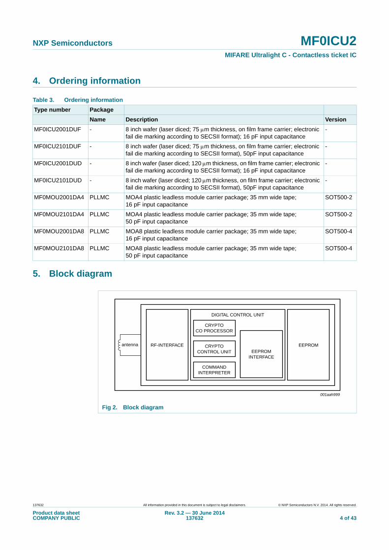
5. Block diagram
Table 3. Ordering information
Type number Package
Name Description Version
MF0ICU2001DUF - 8 inch wafer (laser diced; 75 m thickness, on film frame carrier; electronic fail die marking according to SECSII format); 16 pF input capacitance
-
MF0ICU2101DUF - 8 inch wafer (laser diced; 75 m thickness, on film frame carrier; electronic fail die marking according to SECSII format), 50pF input capacitance
-
MF0ICU2001DUD - 8 inch wafer (laser diced; 120 m thickness, on film frame carrier; electronic fail die marking according to SECSII format); 16 pF input capacitance
-
MF0ICU2101DUD - 8 inch wafer (laser diced; 120 m thickness, on film frame carrier; electronic fail die marking according to SECSII format), 50pF input capacitance
-
MF0MOU2001DA4 PLLMC MOA4 plastic leadless module carrier package; 35 mm wide tape; 16 pF input capacitance
SOT500-2
MF0MOU2101DA4 PLLMC MOA4 plastic leadless module carrier package; 35 mm wide tape; 50 pF input capacitance
SOT500-2
MF0MOU2001DA8 PLLMC MOA8 plastic leadless module carrier package; 35 mm wide tape; 16 pF input capacitance
SOT500-4
MF0MOU2101DA8 PLLMC MOA8 plastic leadless module carrier package; 35 mm wide tape;50 pF input capacitance
SOT500-4
Fig 2. Block diagram
001aah999
antenna RF-INTERFACE
DIGITAL CONTROL UNIT
EEPROM
CRYPTOCO PROCESSOR
CRYPTOCONTROL UNIT
COMMANDINTERPRETER
EEPROMINTERFACE
137632 All information provided in this document is subject to legal disclaimers. © NXP Semiconductors N.V. 2014. All rights reserved.
Product data sheetCOMPANY PUBLIC
Rev. 3.2 — 30 June 2014 137632 4 of 43

NXP Semiconductors MF0ICU2MIFARE Ultralight C - Contactless ticket IC
6. Pinning information
6.1 Smart card contactless module
The pinning is shown as an example in for the MOA4 contactless module. For the contactless module MOA8, the
pinning is analogous and not explicitly shown.
Fig 3. Contact assignments for SOT500-2 (MOA4)
Table 4. Pin allocation table
Antenna contacts Symbol Description
LA LA Antenna coil connection LA
LB LB Antenna coil connection LB
001aaj820
LA LBtop view
137632 All information provided in this document is subject to legal disclaimers. © NXP Semiconductors N.V. 2014. All rights reserved.
Product data sheetCOMPANY PUBLIC
Rev. 3.2 — 30 June 2014 137632 5 of 43

NXP Semiconductors MF0ICU2MIFARE Ultralight C - Contactless ticket IC
7. Functional description
7.1 Block description
The MF0ICU2 chip consists of a 1536-bit EEPROM, an RF-Interface and the Digital Control Unit. Energy and data are transferred via an antenna, which consists of a coil with a few turns directly connected to the MF0ICU2. No further external components are necessary. For details on antenna design please refer to the document Ref. 7.
• RF-Interface:
– Modulator/Demodulator
– Rectifier
– Clock Regenerator
– Power On Reset
– Voltage Regulator
• Crypto coprocessor: Triple - Data Encryption Standard (3DES) coprocessor
• Crypto control unit: controls Crypto coprocessor operations
• Command Interpreter: Handles the commands supported by the MF0ICU2 in order to access the memory
• EEPROM-Interface
• EEPROM: The 1536 bits are organized in 48 pages with 32 bits each. 80 bits are reserved for manufacturer data. 32 bits are used for the read-only locking mechanism. 32 bits are available as OTP area. 1152 bits are user programmable read/write memory.
137632 All information provided in this document is subject to legal disclaimers. © NXP Semiconductors N.V. 2014. All rights reserved.
Product data sheetCOMPANY PUBLIC
Rev. 3.2 — 30 June 2014 137632 6 of 43

NXP Semiconductors MF0ICU2MIFARE Ultralight C - Contactless ticket IC
7.2 State diagram and logical states description
The commands are initiated by the PCD and controlled by the Command Interpreter of the MF0ICU2. It handles the internal states (as shown in Figure 4) and generates the appropriate response.
For a correct implementation of an anticollision procedure please refer to the documents in Section 14.
Remark: In each state the command interpreter returns to the Idle state if an unexpected command is received or any other error occurs. If the IC has already been in the Halt state before it returns to the Halt state in such a case. Those transitions are not explicitly shown in the state diagram.
Fig 4. State diagram
001aai000
AUTHENTICATED
ACTIVE
READY 1
HALTIDLE
POR
SELECTof cascade level 1
READfrom address 0
READfrom address 0
WRITEof 4 byte
WRITEof 4 byte
READof 16 byte
READof 16 byte
ANTICOLLISION
ANTICOLLISION
AUTHENTICATE
REQAWUPA
WUPA
HALT
HALT
SELECTof cascade level 2
READY 2
identificationand
selectionprocedure
memoryoperations
137632 All information provided in this document is subject to legal disclaimers. © NXP Semiconductors N.V. 2014. All rights reserved.
Product data sheetCOMPANY PUBLIC
Rev. 3.2 — 30 June 2014 137632 7 of 43

NXP Semiconductors MF0ICU2MIFARE Ultralight C - Contactless ticket IC
7.2.1 IDLE
After Power On Reset (POR) the MF0ICU2 enters IDLE state. With a REQA or a WUPA command sent from the PCD transits to the READY1 state. Any other data received in this state is interpreted as an error and the MF0ICU2 remains waiting in the Idle state.
Please refer to Ref. 4 for implementation hints for a card polling algorithm that respects relevant timing specifications from ISO/IEC 14443 Type A.
After a correctly executed HLTA command i.e. out of the ACTIVE or AUTHENTICATED state, the default waiting state changes from the IDLE state to the HALT state. This state can then be exited with a WUPA command only.
7.2.2 READY1
In the READY1 state the MF0ICU2 supports the PCD in resolving the first part of its UID (3 bytes) with the ANTICOLLISION or a cascade level 1 SELECT command.
There are two possibilities to leave this state:
• With the cascade level 1 SELECT command the PCD transits the MF0ICU2 into the READY2 state where the second part of the UID can be resolved
• With the READ (from page address 00h) command the complete anticollision mechanism may be skipped and the MF0ICU2 changes directly into the ACTIVE state
Remark: If more than one MF0ICU2 is in the field of the PCD, a read from address 0 will cause a collision because of the different serial numbers, but all MF0ICU2 devices will be selected.
Remark: Any other data received in state READY1 state is interpreted as an error and the MF0ICU2 falls back to its waiting state (IDLE or HALT, depending on its previous state).
The response of the MF0ICU2 to the cascade level 1 SELECT command is the SAK byte with value 04h. It indicates that the UID has not been complete received by the PCD yet and another anticollision level is required.
7.2.3 READY2
In the READY2 state the MF0ICU2 supports the PCD in resolving the second part of its UID (4 bytes) with the ANTICOLLISION command of cascade level 2. This state is left with the cascade level 2 SELECT command.
Alternatively, state READY2 state may be skipped via a READ (from block address 00h) command as described in state READY1.
Remark: If more than one MF0ICU2 is in the field of the PCD, a read from address 00h will cause a collision because of the different serial numbers, but all MF0ICU2 devices will be selected.
Remark: The response of the MF0ICU2 to the cascade level 2 SELECT command is the SAK byte with value 00h. According to ISO/IEC14443 this byte indicates whether the anticollision cascade procedure is finished (see Ref. 6). In addition it defines for the MIFARE architecture platform the type of the selected device. At this stage the MF0ICU2 is uniquely selected and only a single device will continue communication with the PCD even if other contactless devices are in the field of the PCD.
137632 All information provided in this document is subject to legal disclaimers. © NXP Semiconductors N.V. 2014. All rights reserved.
Product data sheetCOMPANY PUBLIC
Rev. 3.2 — 30 June 2014 137632 8 of 43

NXP Semiconductors MF0ICU2MIFARE Ultralight C - Contactless ticket IC
Any other command received in this state is interpreted as an error and the MF0ICU2 falls back to its waiting state (IDLE or HALT, depending on its previous state).
7.2.4 ACTIVE
In the ACTIVE state READ (16 bytes), WRITE (4 bytes), COMPATIBILITY WRITE (16 bytes) commands or an authentication can be performed.
After a successful authentication the state ”AUTHENTICATED” is reached, see Section 7.2.6.
The ACTIVE state is gratefully exited with the HLTA command and upon reception the MF0ICU2 transits to the HALT state.
Any other command received in this state is interpreted as an error and the MF0ICU2 goes back to its waiting state (IDLE or HALT, depending on its previous state).
7.2.5 HALT
Besides the IDLE state the HALT state constitutes the second waiting state implemented in the MF0ICU2. A MF0ICU2 that has already been processed can be set into this state via the HLTA command. This state helps the PCD to distinguish between already processed cards and cards that have not been selected yet. The only way to get the MF0ICU2 out of this state is the WUPA command or a RF reset. Any other data received in this state is interpreted as an error and the MF0ICU2 remains in this state.
7.2.6 AUTHENTICATED
In the AUTHENTICATED state either a READ or a WRITE command may be performed to memory areas, which are only readable and/or writeable after authentication.
Authentication is performed using the 3DES Authentication described in Section 7.5.5.
7.3 Data integrity
The following mechanisms are implemented in the contactless communication link between PCD and MF0ICU2 to ensure a reliable data transmission:
• 16 bits CRC per block
• Parity bit for each byte
• Bit count checking
• Bit coding to distinguish between "1", "0", and no information
• Channel monitoring (protocol sequence and bit stream analysis)
137632 All information provided in this document is subject to legal disclaimers. © NXP Semiconductors N.V. 2014. All rights reserved.
Product data sheetCOMPANY PUBLIC
Rev. 3.2 — 30 June 2014 137632 9 of 43
NXP Semiconductors MF0ICU2MIFARE Ultralight C - Contactless ticket IC
7.4 RF interface
The RF-interface is implemented according to the standard for contactless smart cards ISO/IEC 14443 Type A (see Ref. 1 and Ref. 2).
The RF-field from the PCD is always present (with short modulation pulses when transmitting), because it is used for the power supply of the card.
For both directions of data communication there is one start bit at the beginning of each frame. Each byte is transmitted with a parity bit (odd parity) at the end. The LSBit of the byte with the lowest byte address within selected page is transmitted first. The maximum frame length is 164 bits (16 data bytes + 2 CRC bytes = 16 * 9 + 2 * 9 + 1 start bit + 1 end bit).
7.5 Memory organization
The 1536-bit EEPROM memory is organized in 48 pages with 32 bits each. In the erased state the EEPROM cells are read as a logical “0”, in the written state as a logical “1”.
7.5.1 UID/serial number
The unique 7 byte serial number (UID) and its two Block Check Character Bytes (BCC) are programmed into the first 9 bytes of the memory. It therefore covers page 00h, page 01h and the first byte of page 02h. The second byte of page 02h is reserved for internal data. Due to security and system requirements these bytes are programmed and write-protected in the production test.
Table 5. Memory organization
Page address Byte number
Decimal Hex 0 1 2 3
0 00h serial number
1 01h serial number
2 02h serial number internal lock bytes lock bytes
3 03h OTP OTP OTP OTP
4 to 39 04h to 27h user memory user memory user memory user memory
40 28h lock bytes lock bytes - -
41 29h 16-bit counter 16-bit counter - -
42 2Ah authentication configuration
43 2Bh authentication configuration
44 to 47 2Ch to 2Fh authentication key
137632 All information provided in this document is subject to legal disclaimers. © NXP Semiconductors N.V. 2014. All rights reserved.
Product data sheetCOMPANY PUBLIC
Rev. 3.2 — 30 June 2014 137632 10 of 43

NXP Semiconductors MF0ICU2MIFARE Ultralight C - Contactless ticket IC
According to ISO/IEC14443-3 BCC0 is defined as CT SN0 SN1 SN2.
Abbreviations CT stays for Cascade Tag byte (88h) and BCC1 is defined as SN3 SN4
SN5 SN6.
SN0 holds the Manufacturer ID for NXP (04h) according to ISO/IEC14443-3 and ISO/IEC 7816-6 AMD.1.
7.5.2 Lock byte 0 and 1
The bits of byte 2 and byte 3 of page 02h represent the field programmable permanent read-only locking mechanism. Each page from 03h (OTP) to 0Fh can be individually locked by setting the corresponding locking bit Lx to logic 1 to prevent further write access. After locking, the corresponding page becomes read-only memory. To restrict read access to the memory refer to the authentication functionality (see Section 7.5.5).
The three least significant bits of lock byte 0 are the block-locking bits. Bit 2 deals with pages 0Ah to 0Fh, bit 1 deals with pages 04h to 09h and bit 0 deals with page 03h (OTP). Once the block-locking bits are set, the locking configuration for the corresponding memory area is frozen. The functionality of the bits inside the lock bytes 0 and 1 are shown in Table 6.
For example if BL15-10 is set to logic 1, then bits L15 to L10 (lock byte 1, bit[7:2]) can no longer be changed. A WRITE command or COMPATIBILITY_WRITE command to page 02h, sets the locking and block-locking bits. Byte 2 and byte 3 of the WRITE or COMPATIBILITY_WRITE command, and the contents of the lock bytes are bit-wise OR’ed and the result then becomes the new content of the lock bytes. This process is
Fig 5. UID/serial number
001aai001
MSB LSB
page 0
byte
check byte 0
serial numberpart 1
serial numberpart 2
manufacturer ID for NXP Semiconductors (04h)0 0 0 0 0 1 0 0
0 1 2 3
page 1
0 1 2 3
page 2
0 1 2 3
internal
check byte 1
lock bytes
Fig 6. Lock bytes 0 and 1
aaa-006277
L7
L6
L5
L4
LOTP
BL15-10
BL9-4
BLOTP
MSB
0
page 2
Lx locks page x to read-only
BLx blocks further locking for the memory area x
lock byte 0
lock byte 1
1 2 3
LSB
L15
L14
L13
L12
L11
L10
L9
L8
MSB LSB
137632 All information provided in this document is subject to legal disclaimers. © NXP Semiconductors N.V. 2014. All rights reserved.
Product data sheetCOMPANY PUBLIC
Rev. 3.2 — 30 June 2014 137632 11 of 43

NXP Semiconductors MF0ICU2MIFARE Ultralight C - Contactless ticket IC
irreversible. If a bit is set to logic 1, it cannot be changed back to logic 0. Therefore, before writing the lock bytes, the user has to ensure that the corresponding user memory area and/or configuration bytes to be locked are correctly written.
The contents of bytes 0 and 1 of page 02h are unaffected by the corresponding data bytes of the WRITE (see Section 9.3) or COMPATIBILITY_WRITE (see Section 9.4) command.
The default value of the static lock bytes is 00 00h.
For compatibility reasons, the first 512 bits of the memory area have the same functionality as the MIFARE Ultralight MF0ICU1 (see also Ref. 8), meaning that the two lock bytes used for the configuration of this memory area have identical functionality. The mapping of single lock bits to memory area for the first 512 bits is shown in Figure 6 and Table 6.
Any write operation to the lock bytes 0 and 1, features anti-tearing support.
Remark: The configuration written in the lock bytes is valid upon the next REQA or WUPA command.
7.5.3 Lock byte 2 and 3
To lock the pages of the MF0UL21 starting at page address 10h onwards, the lock bytes 2 and 3 located in page 28h (byte 0 and 1 as shown in Figure 7) are used. Those two lock bytes cover the memory area of 96 data bytes in pages 10h (16d) to 27h (39d) and the configuration area from page address 28h onwards. The granularity is 4 pages, compared to a single page for the first 512 bits as shown in Figure 7. The functionality of the bits inside the lock bytes 2 and 3 are shown in Table 7.
Remark: Set all bits marked with RFUI to 0, when writing to the lock bytes.
Table 6. Functionality of lock bits in lock byte 0 and 1
Lock Byte Bit Function Block Locking in Lock Byte
Block Locking in Bit
0 3 lock OTP page 0 0
0 4 lock page 4 0 1
0 5 lock page 5 0 1
0 6 lock page 6 0 1
0 7 lock page 7 0 1
1 0 lock page 8 0 1
1 1 lock page 9 0 1
1 2 lock page 10 0 2
1 3 lock page 11 0 2
1 4 lock page 12 0 2
1 5 lock page 13 0 2
1 6 lock page 14 0 2
1 7 lock page 15 0 2
137632 All information provided in this document is subject to legal disclaimers. © NXP Semiconductors N.V. 2014. All rights reserved.
Product data sheetCOMPANY PUBLIC
Rev. 3.2 — 30 June 2014 137632 12 of 43

NXP Semiconductors MF0ICU2MIFARE Ultralight C - Contactless ticket IC
The default value of lock bytes 2 and 3 is 00 00h. The value of byte 3 on page 28h (see Figure 7) is always BDh when read.
The contents of bytes 2 and 3 of page 28h are unaffected by the corresponding data bytes of the WRITE (see Section 9.3) or COMPATIBILITY_WRITE (see Section 9.4) command.
Any write operation to the lock bytes 2 and 3, features anti-tearing support.
Remark: The configuration written in the lock bytes is valid upon the next REQA or WUPA command.
7.5.4 OTP bytes
Page 3 is the OTP page. It is preset to all “0” after production. These bytes may be bit-wise modified by the WRITE or COMPATIBILITY WRITE command.
Fig 7. Lock bytes 2 and 3
Table 7. Functionality of lock bits in lock byte 2 and 3
Lock Byte Bit Function Block Locking in Lock Byte
Block Locking in Bit
2 1 lock page 16-19 2 0
2 2 lock page 20-23 2 0
2 3 lock page 24-27 2 0
2 5 lock page 28-31 2 4
2 6 lock page 32-35 2 4
2 7 lock page 36-39 2 4
3 4 lock Counter 3 0
3 5 lock AUTH0 3 1
3 6 lock AUTH1 3 2
3 7 lock Key 3 3
aaa-013580
BLO
CK
LO
CK
ING
PAG
ES
16
- 27
LOC
K P
AG
E36
- 39
LOC
K P
AG
E32
- 35
LOC
K P
AG
E28
- 31
BLO
CK
LO
CK
ING
PAG
ES
29
- 39
LOC
K P
AG
E24
- 27
LOC
K P
AG
E20
- 23
LOC
K P
AG
E16
- 19
BLO
CK
LO
CK
ING
LOC
KB
IT A
UTH
1
BLO
CK
LO
CK
ING
LOC
KB
IT K
EY
BLO
CK
LO
CK
ING
LOC
KB
IT A
UTH
0
BLO
CK
LO
CK
ING
LOC
KB
IT C
NT
LOC
KB
IT A
UTH
1PA
GE
43
LOC
KB
IT A
UTH
0PA
GE
42
LOC
KB
IT C
NT
PAG
E 4
1
LOC
KB
IT K
EY
PAG
E 4
4 - 4
7
MSB
6 5 4 3 2 1 bit 7 6 5 4 3
LSB MSB LSB
page 40 (28h) 10 2 3
0bit 7 0 12
137632 All information provided in this document is subject to legal disclaimers. © NXP Semiconductors N.V. 2014. All rights reserved.
Product data sheetCOMPANY PUBLIC
Rev. 3.2 — 30 June 2014 137632 13 of 43

NXP Semiconductors MF0ICU2MIFARE Ultralight C - Contactless ticket IC
The bytes of the WRITE command and the current contents of the OTP bytes are bit-wise “OR-ed” and the result forms the new content of the OTP bytes. This process is irreversible. If a bit is set to “1”, it cannot be changed back to “0” again.
The default value of the OTP bytes is 00 00 00 00h.
Any write operation to the OTP bytes features anti-tearing support.
(1) Remark: This memory area may be used as a 32 ticks one-time counter.
Fig 8. OTP bytes
001aai004
page 3 default valueEXAMPLE
OTP bytesbyte
OTP bytes
0 1 2 3 00000000 00000000 00000000 00000000
1st write command to page 311111111 11111100 00000101 00000111
result in page 311111111 11111100 00000101 00000111
2nd write command to page 311111111 00000000 00111001 10000000
result in page 311111111 11111100 00111101 10000111
137632 All information provided in this document is subject to legal disclaimers. © NXP Semiconductors N.V. 2014. All rights reserved.
Product data sheetCOMPANY PUBLIC
Rev. 3.2 — 30 June 2014 137632 14 of 43
NXP Semiconductors MF0ICU2MIFARE Ultralight C - Contactless ticket IC
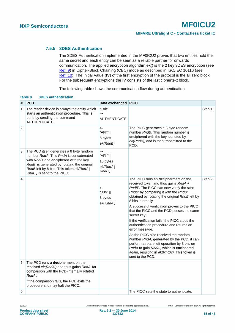
7.5.5 3DES Authentication
The 3DES Authentication implemented in the MF0ICU2 proves that two entities hold the same secret and each entity can be seen as a reliable partner for onwards communication. The applied encryption algorithm ek() is the 2 key 3DES encryption (see Ref. 9) in Cipher-Block Chaining (CBC) mode as described in ISO/IEC 10116 (see Ref. 10). The Initial Value (IV) of the first encryption of the protocol is the all zero block. For the subsequent encryptions the IV consists of the last ciphertext block.
The following table shows the communication flow during authentication:
Table 8. 3DES authentication
# PCD Data exchanged PICC
1 The reader device is always the entity which starts an authentication procedure. This is done by sending the command AUTHENTICATE.
“1Ah”
AUTHENTICATE
Step 1
2 “AFh” ||
8 bytes
ek(RndB)
The PICC generates a 8 byte random number RndB. This random number is enciphered with the key, denoted by ek(RndB), and is then transmitted to the PCD.
3 The PCD itself generates a 8 byte random number RndA. This RndA is concatenated with RndB’ and enciphered with the key. RndB’ is generated by rotating the original RndB left by 8 bits. This token ek(RndA RndB’) is sent to the PICC.
“AFh” ||
16 bytes
ek(RndA RndB’)
4
“00h” ||
8 bytes
ek(RndA’)
The PICC runs an decipherment on the received token and thus gains RndA + RndB’. The PICC can now verify the sent RndB’ by comparing it with the RndB’ obtained by rotating the original RndB left by 8 bits internally.
A successful verification proves to the PICC that the PICC and the PCD posses the same secret key.
If the verification fails, the PICC stops the authentication procedure and returns an error message.
As the PICC also received the random number RndA, generated by the PCD, it can perform a rotate left operation by 8 bits on RndA to gain RndA’, which is enciphered again, resulting in ek(RndA’). This token is sent to the PCD.
Step 2
5 The PCD runs a decipherment on the received ek(RndA’) and thus gains RndA’ for comparison with the PCD-internally rotated RndA’.
If the comparison fails, the PCD exits the procedure and may halt the PICC.
6 The PICC sets the state to authenticate.
137632 All information provided in this document is subject to legal disclaimers. © NXP Semiconductors N.V. 2014. All rights reserved.
Product data sheetCOMPANY PUBLIC
Rev. 3.2 — 30 June 2014 137632 15 of 43

NXP Semiconductors MF0ICU2MIFARE Ultralight C - Contactless ticket IC
The cryptographic method is based on 3DES in CBC mode.
See command details in Section 9.5. The used key is a double length DES Key; where the parity bits are not checked or used.
7.5.6 3DES Authentication example
A numerical example of a 3DES authentication process is shown below in Table 9. The key used in the example has a value of 49454D4B41455242214E4143554F5946h.
Table 9. Numerical 3DES authentication example
# PCD Data exchanged PICC
1 start the authentication procedure 1Ah
2 AF577293FD2F34CA51
generate RndB = 51E764602678DF2BIV = 0000000000000000
ek(RndB) = 577293FD2F34CA51
3 decipher ek(RndB) to retrieve RndBgenerate RndA = A8AF3B256C75ED40RndB’ = E764602678DF2B51RndA+RndB’ = A8AF3B256C75ED40E764602678DF2B51IV = 577293FD2F34CA51ek(RndA+RndB´) = 0A638559FC7737F9F15D7862EBBE967A
AF0A638559FC7737F9F15D7862EBBE967A
4 003B884FA07C137CE1
decipher ek(RndA+RndB´) to retrieve RndAverify RndB’RndA’=AF3B256C75ED40A8IV = F15D7862EBBE967Aek(RndA´)= 3B884FA07C137CE1
5 decipher and verify ek(RndA’)
137632 All information provided in this document is subject to legal disclaimers. © NXP Semiconductors N.V. 2014. All rights reserved.
Product data sheetCOMPANY PUBLIC
Rev. 3.2 — 30 June 2014 137632 16 of 43

NXP Semiconductors MF0ICU2MIFARE Ultralight C - Contactless ticket IC
7.5.7 Programming of 3DES key to memory
The 16 bytes of the 3DES key are programmed to memory pages from 2Ch to 2Fh. The keys are stored in memory as shown in Table 10. The key itself can be written during personalization or at any later stage using the WRITE (see Section 9.3) or COMPATIBILITY WRITE (see Section 9.4) command. For both commands, Byte 0 is always sent first.
On example of Key1 = 0001020304050607h and Key2 = 08090A0B0C0D0E0Fh, the command sequence needed for key programming with WRITE command is:
• A2 2C 07 06 05 04 CRC
• A2 2D 03 02 01 00 CRC
• A2 2E 0F 0E 0D 0C CRC
• A2 2F 0B 0A 09 08 CRC
The memory content after those (COMPATIBILITY) WRITE commands is shown in Table 11.
The memory pages holding the authentication key can never be read, independent of the configuration.
Remark: A re-programmed authentication key is only valid for authentication after a RF reset or a re-activation.
Table 10. Key memory configuration
Byte address 0h 1h 2h 3h
Page address Byte 0 Byte 1 Byte 2 Byte 3
2Ch Page 44 Key1 / K0 Key1 / K1 Key1 / K2 Key1 / K3
2Dh Page 45 Key1 / K4 Key1 / K5 Key1 / K6 Key1 / K7
2Eh Page 46 Key2 / K0 Key2 / K1 Key2 / K2 Key2 / K3
2Fh Page 47 Key2 / K4 Key2 / K5 Key2 / K6 Key2 / K7
Table 11. Memory content based on example configuration
Byte address 0h 1h 2h 3h
Page address Byte 0 Byte 1 Byte 2 Byte 3
2Ch Page 44 07 06 05 04
2Dh Page 45 03 02 01 00
2Eh Page 46 0F 0E 0D 0C
2Fh Page 47 0B 0A 09 08
137632 All information provided in this document is subject to legal disclaimers. © NXP Semiconductors N.V. 2014. All rights reserved.
Product data sheetCOMPANY PUBLIC
Rev. 3.2 — 30 June 2014 137632 17 of 43

NXP Semiconductors MF0ICU2MIFARE Ultralight C - Contactless ticket IC
7.5.8 Configuration for memory access via 3DES Authentication
The behavior of the memory access rights depending on the authentication is configured with two configuration bytes, AUTH0 and AUTH1, located in pages 2Ah and 2Bh. Both configuration bytes are located in Byte 0 of the respective pages (see also Table 5).
• AUTH0 defines the page address from which the authentication is required. Valid address values for byte AUTH0 are from 03h to 30h.
• Setting AUTH0 to 30h effectively disables memory protection.
• AUTH1 determines if write access is restricted or both read and write access are restricted, see Table 12
7.5.9 Data pages
The MF0ICU2 features 144 bytes of data memory. The user memory area ranges from page 04h to 27h.
Initial state of each byte in the user area is 00h.
A write access to data memory is done with a WRITE (see Section 9.3) or a COMPATIBILITY WRITE (see Section 9.4) command. In both cases, 4 bytes of memory - (one page) - will be written. Write access to data memory can be permanently restricted via lock bytes (see Section 7.5.2 and Section 7.5.3) and/or permanently or temporary restricted using an authentication (see Section 7.5.5).
Reading data is done using the READ command (see Section 9.2).
Table 12. AUTH1 bit description
Bit Value Description
1 to 7 any ignored
0 1 write access restricted, read access allowed without authentication
0 read and write access restricted
137632 All information provided in this document is subject to legal disclaimers. © NXP Semiconductors N.V. 2014. All rights reserved.
Product data sheetCOMPANY PUBLIC
Rev. 3.2 — 30 June 2014 137632 18 of 43
NXP Semiconductors MF0ICU2MIFARE Ultralight C - Contactless ticket IC
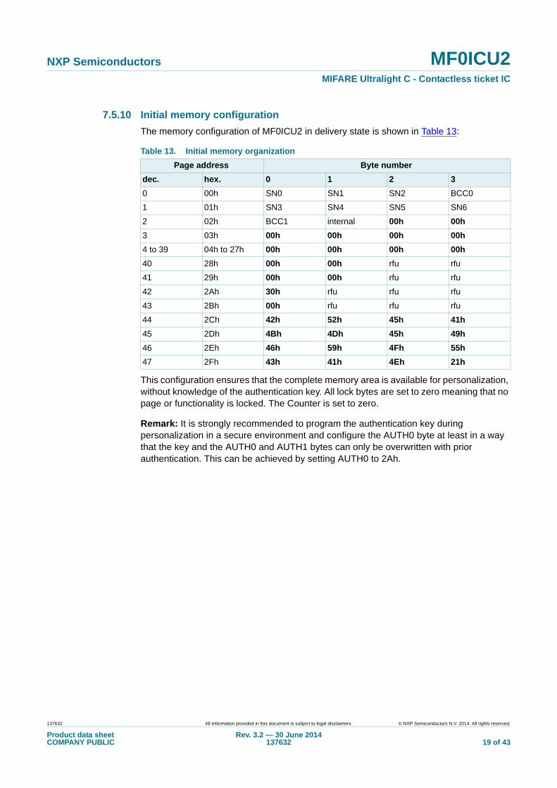
7.5.10 Initial memory configuration
The memory configuration of MF0ICU2 in delivery state is shown in Table 13:
This configuration ensures that the complete memory area is available for personalization, without knowledge of the authentication key. All lock bytes are set to zero meaning that no page or functionality is locked. The Counter is set to zero.
Remark: It is strongly recommended to program the authentication key during personalization in a secure environment and configure the AUTH0 byte at least in a way that the key and the AUTH0 and AUTH1 bytes can only be overwritten with prior authentication. This can be achieved by setting AUTH0 to 2Ah.
Table 13. Initial memory organization
Page address Byte number
dec. hex. 0 1 2 3
0 00h SN0 SN1 SN2 BCC0
1 01h SN3 SN4 SN5 SN6
2 02h BCC1 internal 00h 00h
3 03h 00h 00h 00h 00h
4 to 39 04h to 27h 00h 00h 00h 00h
40 28h 00h 00h rfu rfu
41 29h 00h 00h rfu rfu
42 2Ah 30h rfu rfu rfu
43 2Bh 00h rfu rfu rfu
44 2Ch 42h 52h 45h 41h
45 2Dh 4Bh 4Dh 45h 49h
46 2Eh 46h 59h 4Fh 55h
47 2Fh 43h 41h 4Eh 21h
137632 All information provided in this document is subject to legal disclaimers. © NXP Semiconductors N.V. 2014. All rights reserved.
Product data sheetCOMPANY PUBLIC
Rev. 3.2 — 30 June 2014 137632 19 of 43
NXP Semiconductors MF0ICU2MIFARE Ultralight C - Contactless ticket IC
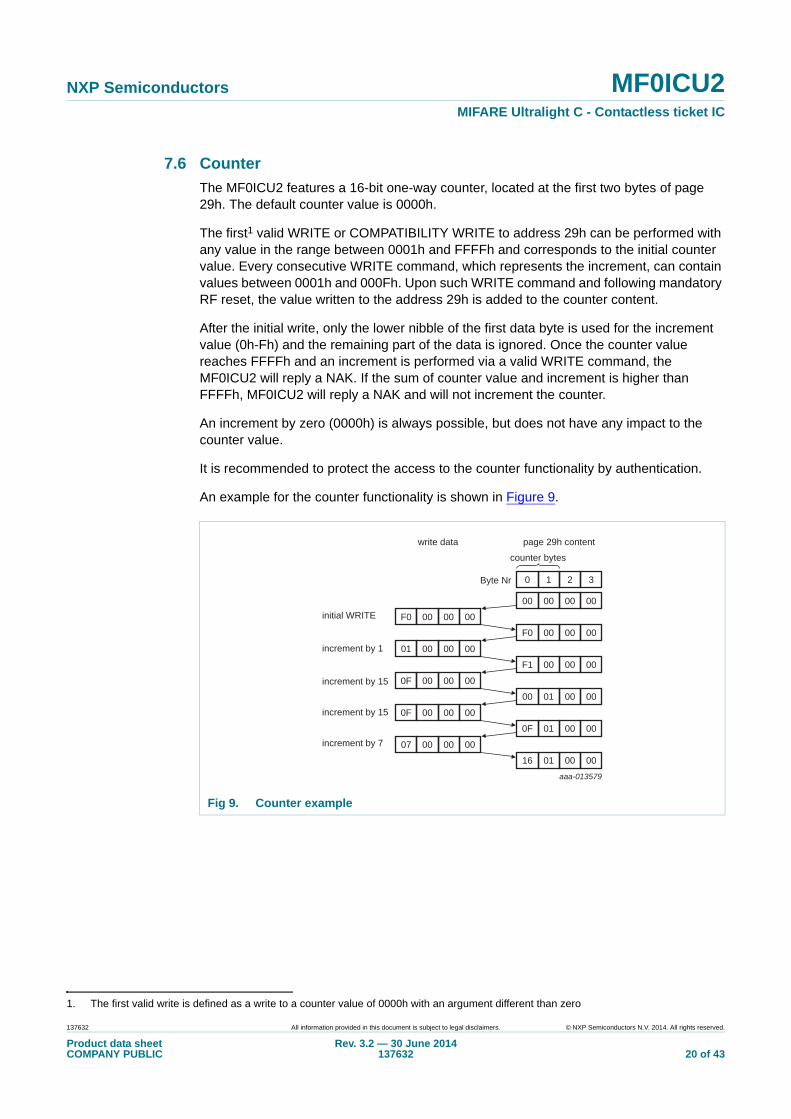
7.6 Counter
The MF0ICU2 features a 16-bit one-way counter, located at the first two bytes of page 29h. The default counter value is 0000h.
The first1 valid WRITE or COMPATIBILITY WRITE to address 29h can be performed with any value in the range between 0001h and FFFFh and corresponds to the initial counter value. Every consecutive WRITE command, which represents the increment, can contain values between 0001h and 000Fh. Upon such WRITE command and following mandatory RF reset, the value written to the address 29h is added to the counter content.
After the initial write, only the lower nibble of the first data byte is used for the increment value (0h-Fh) and the remaining part of the data is ignored. Once the counter value reaches FFFFh and an increment is performed via a valid WRITE command, the MF0ICU2 will reply a NAK. If the sum of counter value and increment is higher than FFFFh, MF0ICU2 will reply a NAK and will not increment the counter.
An increment by zero (0000h) is always possible, but does not have any impact to the counter value.
It is recommended to protect the access to the counter functionality by authentication.
An example for the counter functionality is shown in Figure 9.
1. The first valid write is defined as a write to a counter value of 0000h with an argument different than zero
Fig 9. Counter example
aaa-013579
page 29h contentwrite data
counter bytes
00 00 00 00
F0 00 00 00
F1 00 00 00
00 01 00 00
0F 01 00 00
16 01 00 00
F0 00 00 00
01 00 00 00
0F 00 00 00
0F 00 00 00
07 00 00 00
0 1 2 3Byte Nr
increment by 1
initial WRITE
increment by 15
increment by 15
increment by 7
137632 All information provided in this document is subject to legal disclaimers. © NXP Semiconductors N.V. 2014. All rights reserved.
Product data sheetCOMPANY PUBLIC
Rev. 3.2 — 30 June 2014 137632 20 of 43

NXP Semiconductors MF0ICU2MIFARE Ultralight C - Contactless ticket IC
8. Command overview
The MIFARE Ultralight C card activation follows the ISO/IEC 14443 Type A. After the MIFARE Ultralight C card has been selected, it can either be deactivated using the ISO/IEC 14443 Halt command, or the MIFARE Ultralight C commands can be performed. For more details about the card activation refer to Ref. 2.
8.1 MIFARE Ultralight C command overview
All available commands for the MIFARE Ultralight C are shown in Table 14. All memory access commands are transmitted in plain, only the AUTHENTICATE command uses 3DES encryption, see Section 9.5.
All commands use the coding and framing as described in Ref. 1 and Ref. 2 if not otherwise specified.
Table 14. Command overview
Command ISO/IEC 14443 Command code (hexadecimal)
Request REQA 26h (7 bit)
Wake-up WUPA 52h (7 bit)
Anticollision CL1 Anticollision CL1 93h 20h
Select CL1 Select CL1 93h 70h
Anticollision CL2 Anticollision CL2 95h 20h
Select CL2 Select CL2 95h 70h
Halt Halt 50h 00h
READ - 30h
WRITE - A2h
COMPATIBILITY WRITE - A0h
AUTHENTICATE - 1Ah
137632 All information provided in this document is subject to legal disclaimers. © NXP Semiconductors N.V. 2014. All rights reserved.
Product data sheetCOMPANY PUBLIC
Rev. 3.2 — 30 June 2014 137632 21 of 43

NXP Semiconductors MF0ICU2MIFARE Ultralight C - Contactless ticket IC
8.2 Timings
The timing shown in this document are not to scale and values are rounded to 1 s.
All given command and response transmission times refer to the data frames including start of communication and end of communication. A PCD data frame contains the start of communication (1 “start bit”) and the end of communication (one logic 0 + 1 bit length of unmodulated carrier). A PICC data frame contains the start of communication (1 “start bit”) and the end of communication (1 bit length of no subcarrier).
The minimum command response time is specified according to Ref. 2 as an integer n which specifies the PCD to PICC frame delay time. The frame delay time (FDT) from PICC to PCD is at least 87 s which corresponds to a n=9. The maximum command response time is specified as a time-out value. Depending on the command, the TACK value specified for command responses defines the PCD to PICC frame delay time. It does it for either the 4-bit ACK/NAK value specified in Section 8.3 or for a data frame.
All command timings are according to ISO/IEC 14443-3 frame specification as shown for the Frame Delay Time in Figure 10. For more details refer to Ref. 1 and Ref. 2.
Remark: Due to the coding of commands, the measured timings usually excludes (a part of) the end of communication. Consider this factor when comparing the specified with the measured times.
8.3 MIFARE Ultralight C ACK and NAK
The MIFARE Ultralight C - Contactless ticket IC uses, apart from the responses defined in the following sections, two half-byte answers to acknowledge the command received in ACTIVE and AUTHENTICATED state (see Figure 4) abbreviated as ACK and NAK.
The MIFARE Ultralight C - Contactless ticket IC distinguishes between positive (ACK) and negative (NAK) acknowledge. Valid values for ACK and NAK are shown in Table 15.
Fig 10. Frame Delay Time (from PCD to PICC) and TACK and TNAK
aaa-006279
last data bit transmitted by the PCD
FDT = (n* 128 + 84)/fc
first modulation of the PICC
FDT = (n* 128 + 20)/fc
128/fc logic „1“
128/fc logic „0“
256/fcend of communication (E)
256/fcend of communication (E)
128/fc start of
communication (S)
128/fc start of
communication (S)
137632 All information provided in this document is subject to legal disclaimers. © NXP Semiconductors N.V. 2014. All rights reserved.
Product data sheetCOMPANY PUBLIC
Rev. 3.2 — 30 June 2014 137632 22 of 43

NXP Semiconductors MF0ICU2MIFARE Ultralight C - Contactless ticket IC
After every NAK, the MF0ICU2 performs an internal reset and returns to IDLE or HALT state.
Remark: Any 4-bit response different from Ah shall be interpreted as NAK, although not all 4-bit values are detailed in Table 15
8.4 Summary of device identification data
For more details on the values below please refer to Ref. 2, Ref. 3 and Ref. 4.
Table 15. ACK and NAK values
Answer value Answer explanation
Ah positive acknowledge (ACK)
2h NAK for EEPROM write error
1h NAK for parity or CRC error
0h NAK for any other error
Table 16. Summary of relevant data for device identification
Code Length Value Binary Format Remark
ATQA 2 Byte 0044h 0000 0000 0100 0100
CT 1 Byte 88h 1000 1000 Cascade Tag, ensures collision with cascade level 1 products
SAK (casc. level 1) 1 Byte 04h 0000 0100 ‘1’ indicates additional cascade level
SAK (casc. level 2) 1 Byte 00h 0000 0000 indicates complete UID and MIFARE Ultralight functionality
Manufacturer Byte 1 Byte 04h 0000 0100 indicates NXP Semiconductors as manufacturer
137632 All information provided in this document is subject to legal disclaimers. © NXP Semiconductors N.V. 2014. All rights reserved.
Product data sheetCOMPANY PUBLIC
Rev. 3.2 — 30 June 2014 137632 23 of 43

NXP Semiconductors MF0ICU2MIFARE Ultralight C - Contactless ticket IC
9. MIFARE Ultralight C - Contactless ticket IC commands
9.1 MIFARE Ultralight C - Contactless ticket IC card activation
The ATQA and SAK values are identical as for MF0ICU1 (see Ref. 8). For information on ISO 14443 card activation, see Ref. 4. Summary of data relevant for device identification is given in Section 8.4.
9.2 READ
The READ command takes the page address as a parameter. Only addresses 00h to 2Bh are decoded. For higher addresses the MF0ICU2 returns a NAK. The MF0ICU2 responds to the READ command by sending 16 bytes starting from the page address defined in the command (e.g. if ADR is 03h, pages 03h, 04h, 05h, 06h are returned). The command structure is shown in Figure 11 and Table 17.
Table 18 shows the required timing.
A roll-over mechanism is implemented to continue reading from page 00h once the end of the accessible memory is reached. For example, reading from address 29h on a MF0ICU2 results in pages 29h, 2Ah, 2Bh and 00h being returned.
The following conditions apply if part of the memory is protected by the 3DES authentication for read access:
• if the MF0ICU2 is in the ACTIVE state
– addressing a page which is equal or higher than AUTH0 results in a NAK response
– addressing a page lower than AUTH0 results in data being returned with the roll-over mechanism occurring just before the AUTH0 defined page
• if the MF0ICU2 is in the AUTHENTICATED state
– the READ command behaves like on a MF0ICU2 without access protection
Fig 11. READ
aaa-006284
CRC
CRC
AddrPCD Cmd
DataPICC ,,ACK''
368 µs 1548 µs
PICC ,,NAK'' NAK
Time out TTimeOut
TNAK
TACK
57 µs
137632 All information provided in this document is subject to legal disclaimers. © NXP Semiconductors N.V. 2014. All rights reserved.
Product data sheetCOMPANY PUBLIC
Rev. 3.2 — 30 June 2014 137632 24 of 43

NXP Semiconductors MF0ICU2MIFARE Ultralight C - Contactless ticket IC
Table 17. READ command
Name Code Description Length
Cmd 30h read four pages 1 byte
Addr - start page address ‘00h’ to ‘2Bh‘ 1 byte
CRC - CRC according to Ref. 2 2 bytes
Data - data content of the addressed pages 16 bytes
NAK see Table 15 see Section 8.3 4-bit
Table 18. READ timingThese times exclude the end of communication of the PCD.
TACK min TACK max TNAK min TNAK max TTimeOut
READ n=9 TTimeOut n=9 TTimeOut 5 ms
137632 All information provided in this document is subject to legal disclaimers. © NXP Semiconductors N.V. 2014. All rights reserved.
Product data sheetCOMPANY PUBLIC
Rev. 3.2 — 30 June 2014 137632 25 of 43

NXP Semiconductors MF0ICU2MIFARE Ultralight C - Contactless ticket IC
9.3 WRITE
The WRITE command is used to program the lock bytes in page 02h, the OTP bytes in page 03h, data bytes in pages 04h to 27h, configuration data from page 28h to 2B and keys from page 2Ch to 2Fh. A WRITE command is performed page-wise, programming 4 bytes in a page.The WRITE command is shown in Figure 12 and Table 19.
Table 20 shows the required timing.
Fig 12. WRITE
Table 19. WRITE command
Name Code Description Length
Cmd A2h write one page 1 byte
Addr - page address ‘02h’ to ‘2Fh’ 1 byte
CRC - CRC according to Ref. 2 2 bytes
Data - data 4 bytes
NAK see Table 15 see Section 8.3 4-bit
Table 20. WRITE timingThese times exclude the end of communication of the PCD.
TACK min TACK max TNAK min TNAK max TTimeOut
WRITE n=9 TTimeOut n=9 TTimeOut 10 ms
aaa-006286
CRCAddrPCD Cmd
PICC ,,ACK''
708 µs
PICC ,,NAK'' NAK
Time out TTimeOut
TNAK
TACK
57 µs
ACK
57 µs
Data
137632 All information provided in this document is subject to legal disclaimers. © NXP Semiconductors N.V. 2014. All rights reserved.
Product data sheetCOMPANY PUBLIC
Rev. 3.2 — 30 June 2014 137632 26 of 43

NXP Semiconductors MF0ICU2MIFARE Ultralight C - Contactless ticket IC
9.4 COMPATIBILITY WRITE
The COMPATIBILITY WRITE command was implemented to accommodate the established MIFARE PCD infrastructure. Even though 16 bytes are transferred to the MF0ICU2, only the least significant 4 bytes (bytes 0 to 3) will be written to the specified address. It is recommended to set the remaining bytes 4 to 15 to all ‘0’.
Personalization of authentication key: For writing the authentication key, one needs to write the key with four commands. The first command shall have the 4 least significant bytes of the key and shall be written on page 2Ch, the second 4 bytes shall be written on page 2Dh, the next 4 bytes shall be written on page 2Eh, the last 4 bytes shall be written on page 2Fh.
Fig 13. COMPATIBILITY WRITE part 1
Fig 14. COMPATIBILITY WRITE part 2
001aan015
CRCAddrPCD Cmd
PICC ,,ACK''
368 μs
PICC ,,NAK'' NAK
Time out TTimeOut
TNAK
TACK
59 μs
ACK
59 μs
001aan016
CRCPCD Data
PICC ,,ACK''
1558 μs
PICC ,,NAK'' NAK
Time out TTimeOut
TNAK
TACK
59 μs
ACK
59 μs
137632 All information provided in this document is subject to legal disclaimers. © NXP Semiconductors N.V. 2014. All rights reserved.
Product data sheetCOMPANY PUBLIC
Rev. 3.2 — 30 June 2014 137632 27 of 43

NXP Semiconductors MF0ICU2MIFARE Ultralight C - Contactless ticket IC
Table 21. COMPATIBILITY_WRITE command
Name Code Description Length
Cmd A0h compatibility write 1 byte
Addr - page address ‘02h’ to ‘2Fh’ 1 byte
CRC - CRC according to Ref. 2 2 bytes
Data - 16-byte Data, only least significant 4 bytes are written
16 bytes
NAK see Table 15 see Section 8.3 4-bit
Table 22. COMPATIBILITY_WRITE timingThese times exclude the end of communication of the PCD.
TACK min TACK max TNAK min TNAK max TTimeOut
COMPATIBILITY_WRITE part 1 n=9 TTimeOut n=9 TTimeOut 5 ms
COMPATIBILITY_WRITE part 2 n=9 TTimeOut n=9 TTimeOut 10 ms
137632 All information provided in this document is subject to legal disclaimers. © NXP Semiconductors N.V. 2014. All rights reserved.
Product data sheetCOMPANY PUBLIC
Rev. 3.2 — 30 June 2014 137632 28 of 43

NXP Semiconductors MF0ICU2MIFARE Ultralight C - Contactless ticket IC
9.5 AUTHENTICATE
Description: The authentication process is detailed Section 7.5.5.
The command is performed in the same protocol as READ, WRITE and COMPATIBILITY WRITE.
Executing a HALT command results in losing the authentication status.
Fig 15. AUTHENTICATE Step 1
Table 23. AUTHENTICATE part 1 command
Name Code Description Length
Cmd 1Ah authentication part 1 1 byte
Arg 00h fixed value 00h as argument 1 byte
CRC - CRC according to Ref. 2 2 bytes
AFh AFh first response byte indicates that the authentication process needs a second command part
1 bytes
ek(RndB) - 8-byte encrypted PICC random number RndB
8 bytes
NAK see Table 15 see Section 8.3 4-bit
Table 24. AUTHENTICATE part 1 timingThese times exclude the end of communication of the PCD.
TACK min TACK max TNAK min TNAK max TTimeOut
AUTHENTICATE part 1 n=9 TTimeOut n=9 TTimeOut 5 ms
Table 25. AUTHENTICATE Step 2
Code Parameter Data Integrity mechanism Response
AFh - ek(RndA+RndB') Parity, CRC ’00’ + ek(RndA')
aaa-013577
CRC
CRCAFh
ArgPCD Cmd 8 Byte ek(RndB)
D7 D6 D1... D0PICC ,,ACK''
368 µs 953 µs
PICC ,,NAK'' NAK
Time out TTimeOut
TNAK
TACK
57 µs
137632 All information provided in this document is subject to legal disclaimers. © NXP Semiconductors N.V. 2014. All rights reserved.
Product data sheetCOMPANY PUBLIC
Rev. 3.2 — 30 June 2014 137632 29 of 43

NXP Semiconductors MF0ICU2MIFARE Ultralight C - Contactless ticket IC
Fig 16. AUTHENTICATE Step 2
Table 26. AUTHENTICATE part 2 command
Name Code Description Length
Cmd AFh fixed first byte for the AUTHENTICATE part 2 command
1 byte
ek(RndA || RndB’) - 16-byte encrypted random numbers RNDA concatenated by RndB’
16 bytes
CRC - CRC according to Ref. 2 2 bytes
00h 00h first response byte indicates that the authentication process is finished after this command
1 bytes
ek(RndA’) - 8-byte encrypted, shifted PCD random number RndA’
8 bytes
NAK see Table 15 see Section 8.3 4-bit
Table 27. AUTHENTICATE part 2 timingThese times exclude the end of communication of the PCD.
TACK min TACK max TNAK min TNAK max TTimeOut
AUTHENTICATE part 2 n=9 TTimeOut n=9 TTimeOut 5 ms
PICC ,,ACK''
aaa-013578
CRC
16 Byte ek(RndA || RndB’)
PCD Cmd
1642 µs 953 µs
PICC ,,NAK'' NAK
Time out TTimeOut
TNAK
TACK
57 µs
CRC00h
8 Byte ek(RndA’)D7 D6 D1... D0
D7 ... D0 D7 ... D0
137632 All information provided in this document is subject to legal disclaimers. © NXP Semiconductors N.V. 2014. All rights reserved.
Product data sheetCOMPANY PUBLIC
Rev. 3.2 — 30 June 2014 137632 30 of 43

NXP Semiconductors MF0ICU2MIFARE Ultralight C - Contactless ticket IC
10. Limiting values
Stresses exceeding one or more of the limiting values, can cause permanent damage to the device. Exposure to limiting values for extended periods can affect device reliability.
[1] ANSI/ESDA/JEDEC JS-001; Human body model: C = 100 pF, R = 1.5 k
11. Characteristics
11.1 Electrical characteristics
[1] Tamb = 22 C, f = 13.56 MHz, VLaLb = 1.5 V RMS
Table 28. Limiting values In accordance with the Absolute Maximum Rating System (IEC 60134).
Symbol Parameter Min Max Unit
II input current - 30 mA
Tstg storage temperature -55 +125 C
Tamb ambient temperature -25 +70 C
VESD electrostatic discharge voltage on LA/LB [1] 2 - kV
Table 29. Characteristics
Symbol Parameter Conditions Min Typ Max Unit
fi input frequency - 13.56 - MHz
Ci input capacitance 16 pF version (bare silicon and MOA4)
[1] 14.08 16 17.92 pF
50 pF version [1] 44 50 56 pF
EEPROM characteristics
tcy(W) write cycle time - 4.1 - ms
tret retention time Tamb = 22 C 10 - - year
Nendu(W) write endurance Tamb = 22 C 100000 - - cycle
137632 All information provided in this document is subject to legal disclaimers. © NXP Semiconductors N.V. 2014. All rights reserved.
Product data sheetCOMPANY PUBLIC
Rev. 3.2 — 30 June 2014 137632 31 of 43

NXP Semiconductors MF0ICU2MIFARE Ultralight C - Contactless ticket IC
12. Wafer specification
[1] The step size and the gap between chips may vary due to changing foil expansion
[2] Pads VSS and TESTIO are disconnected when wafer is sawn.
12.1 Fail die identification
Electronic wafer mapping covers the electrical test results and additionally the results of mechanical/visual inspection. No ink dots are applied.
Table 30. Wafer specifications MF0ICU2x01DUy
Wafer
diameter 200 mm typical (8 inches)
maximum diameter after foil expansion 210 mm
die separation process laser dicing
thickness MF0ICU2x01XDUD 120 m 15 m
MF0ICU2x01XDUF 75 m 10 m
flatness not applicable
Potential Good Dies per Wafer (PGDW) 61942
Wafer backside
material Si
treatment ground and stress relieve
roughness Ra max = 0.2 m
Rt max = 2 m
Chip dimensions
step size[1] x = 710 m
y = 710 m
gap between chips[1] typical = 22 m
minimum = 5 m
Passivation
type sandwich structure
material PSG / nitride
thickness 500 nm / 600 nm
Au bump (substrate connected to VSS)
material > 99.9 % pure Au
hardness 35 to 80 HV 0.005
shear strength > 70 MPa
height 18 m
height uniformity within a die = 2 m
within a wafer = 3 m
wafer to wafer = 4 m
flatness minimum = 1.5 m
size LA, LB, VSS, TP1, TP2[2] = 60 m 60 m
size variation 5 m
under bump metallization sputtered TiW
137632 All information provided in this document is subject to legal disclaimers. © NXP Semiconductors N.V. 2014. All rights reserved.
Product data sheetCOMPANY PUBLIC
Rev. 3.2 — 30 June 2014 137632 32 of 43

NXP Semiconductors MF0ICU2MIFARE Ultralight C - Contactless ticket IC
12.2 Package outline
For more details on the contactless modules MOA4 and MOA8 please refer to Ref. 11 and Ref. 12.
Fig 17. Package outline SOT500-2
UNIT D
REFERENCESOUTLINEVERSION
EUROPEANPROJECTION ISSUE DATE
IEC JEDEC JEITA
mm 35.0534.95
For unspecified dimensions see PLLMC-drawing given in the subpackage code.
DIMENSIONS (mm are the original dimensions)
SOT500-203-09-1706-05-22- - - - - -- - -
PLLMC: plastic leadless module carrier package; 35 mm wide tape SOT500-2
A(1)
max.
0.33
0 10 20 mm
scale
A
detail X
X
Note1. Total package thickness, exclusive punching burr.
D
137632 All information provided in this document is subject to legal disclaimers. © NXP Semiconductors N.V. 2014. All rights reserved.
Product data sheetCOMPANY PUBLIC
Rev. 3.2 — 30 June 2014 137632 33 of 43

NXP Semiconductors MF0ICU2MIFARE Ultralight C - Contactless ticket IC
Fig 18. Package outline SOT500-4
ReferencesOutlineversion
Europeanprojection Issue date
IEC JEDEC JEITA
SOT500-4 - - -- - -- - -
sot500-4_po
11-02-18
Unit
mmmaxnommin
0.26 35.0535.0034.95
A(1)
Dimensions
Note1. Total package thickness, exclusive punching burr.
PLLMC: plastic leadless module carrier package; 35 mm wide tape SOT500-4
D
For unspecified dimensions see PLLMC-drawing given in the subpackage code.
0 10 20 mm
scale
X
D
detail X
A
137632 All information provided in this document is subject to legal disclaimers. © NXP Semiconductors N.V. 2014. All rights reserved.
Product data sheetCOMPANY PUBLIC
Rev. 3.2 — 30 June 2014 137632 34 of 43

NXP Semiconductors MF0ICU2MIFARE Ultralight C - Contactless ticket IC
12.3 Bare die outline
For more details on the wafer delivery forms see Ref. 13.
Fig 19. Bare die outline MF0ICU2x01DUy
43.5
MF0ICU2
LBTEST
LA
VDD
GND
223.6
typ. 22(1)
min. 5
x [µm] y [µm]
710(1)
60
710(1)
60
Chip StepBump sizeLA, LB, VSS, VDD, TEST
typ. 22(1)
min. 5
49.1
528.6
626
x
y626
typ. 710(1)
the air gap and thus the step size may vary due to varying foil expansionall dimensions in µm, pad locations measured from metal ring edge (see detail)
(1)(2) aaa-013576
typ. 710(1)
137632 All information provided in this document is subject to legal disclaimers. © NXP Semiconductors N.V. 2014. All rights reserved.
Product data sheetCOMPANY PUBLIC
Rev. 3.2 — 30 June 2014 137632 35 of 43

NXP Semiconductors MF0ICU2MIFARE Ultralight C - Contactless ticket IC
13. Abbreviations
Table 31. Abbreviations
Acronym Description
3DES Triple Data Encryption Standard
ACK Positive Acknowledge
ATQA Answer To ReQuest, type A
BCC Block Check Characters byte
CBC Cipher-Block Chaining
CRC Cyclic Redundancy Check
CT Cascade Tag, Type A
EEPROM Electrically Erasable Programmable Read-Only Memory
fc carrier frequency 13.56 MHz
HLTA Halt A command
IV Initial Value
LSB Least Significant Bit
MSB Most Significant Bit
NAK Negative AcKnowledge
OTP One Time Programmable
Passive ACK Implicit acknowledge without PICC answer
PCD Proximity Coupling Device
PICC Proximity Integrated Circuit Card
POR Power On Reset
REQA ReQuest Answer, type A
RF Radio Frequency
SAK Select AcKnowledge, type A
UID Unique Identifier
WUPA Wake-UP command, type A
137632 All information provided in this document is subject to legal disclaimers. © NXP Semiconductors N.V. 2014. All rights reserved.
Product data sheetCOMPANY PUBLIC
Rev. 3.2 — 30 June 2014 137632 36 of 43

NXP Semiconductors MF0ICU2MIFARE Ultralight C - Contactless ticket IC
14. References
[1] ISO/IEC 14443-2 — 2001
[2] ISO/IEC 14443-3 — 2001
[3] MIFARE Interface Platform Type Identification Procedure — Application note, BL-ID Doc. No.: 0184**2
[4] MIFARE ISO/IEC 14443 PICC Selection — Application note,BL-ID Doc. No.: 1308**
[5] MIFARE Ultralight Features and Hints — Application note, BL-ID Doc. No.: 0731**
[6] MIFARE Ultralight as Type 2 Tag — Application note, BL-ID Doc. No.: 1303**
[7] MIFARE (Card) Coil Design Guide — Application note, BL-ID Doc. No.: 0117**
[8] MF0ICU1 Functional specification MIFARE Ultralight — Product data sheet, BL-ID Doc. No. 0286**
[9] NIST SP800-67: Recommendation for the Triple Data Encryption Algorithm (TDEA) Block Cipher, Version 1.1 May 19, 2008 — National Institute of Standards and Technology
[10] ISO/IEC 10116: Information technology - Security techniques - Modes of operation for an n-bit block cipher, February 1, 2006 — International Organization for Standardization
[11] Contactless smart card module specification MOA4 — Delivery Type Description, BU-ID Document number 0823**2
[12] Contactless smart card module specification MOA8 — Delivery Type Description, BU-ID Document number 1636**2
[13] General specification for 8" wafer on UV-tape; delivery types — Delivery Type Description, BU-ID Document number 1005**2
2. ** ... document version number
137632 All information provided in this document is subject to legal disclaimers. © NXP Semiconductors N.V. 2014. All rights reserved.
Product data sheetCOMPANY PUBLIC
Rev. 3.2 — 30 June 2014 137632 37 of 43

NXP Semiconductors MF0ICU2MIFARE Ultralight C - Contactless ticket IC
15. Revision history
Table 32. Revision history
Document ID Release date Data sheet status Change notice Supersedes
MF0ICU2 v. 3.2 20140630 Product data sheet 137631
Modifications: • Editorial changes
• Added 75m thin wafer and MOA8 delivery types
• New bare die outline drawing
• Corrected descriptive text in delivery forms for the 16 pF input capacitance
• Extended EEPROM specification with respect to programming cycle endurance and data retention
• New command descriptions including time-out specification
• Added descriptions for authentication, counter and lock bytes
• Removed ISO/IEC 14443-3 anticollision and selection commands and referred to standard
137631 20090402 Product data sheet 137630
Modifications: • Section 16 “Legal information”: updated
137630 20090218 Product data sheet - 137610
Modifications: • General update
137610 20080428 Objective data sheet - 137601
Modifications: • Update of spelling issues
• Redesign of drawings
• Update of Section 1.3 “Security” on page 2
137601 20080404 Objective data sheet - -
137632 All information provided in this document is subject to legal disclaimers. © NXP Semiconductors N.V. 2014. All rights reserved.
Product data sheetCOMPANY PUBLIC
Rev. 3.2 — 30 June 2014 137632 38 of 43

NXP Semiconductors MF0ICU2MIFARE Ultralight C - Contactless ticket IC
16. Legal information
16.1 Data sheet status
[1] Please consult the most recently issued document before initiating or completing a design.
[2] The term ‘short data sheet’ is explained in section “Definitions”.
[3] The product status of device(s) described in this document may have changed since this document was published and may differ in case of multiple devices. The latest product status information is available on the Internet at URL http://www.nxp.com.
16.2 Definitions
Draft — The document is a draft version only. The content is still under internal review and subject to formal approval, which may result in modifications or additions. NXP Semiconductors does not give any representations or warranties as to the accuracy or completeness of information included herein and shall have no liability for the consequences of use of such information.
Short data sheet — A short data sheet is an extract from a full data sheet with the same product type number(s) and title. A short data sheet is intended for quick reference only and should not be relied upon to contain detailed and full information. For detailed and full information see the relevant full data sheet, which is available on request via the local NXP Semiconductors sales office. In case of any inconsistency or conflict with the short data sheet, the full data sheet shall prevail.
Product specification — The information and data provided in a Product data sheet shall define the specification of the product as agreed between NXP Semiconductors and its customer, unless NXP Semiconductors and customer have explicitly agreed otherwise in writing. In no event however, shall an agreement be valid in which the NXP Semiconductors product is deemed to offer functions and qualities beyond those described in the Product data sheet.
16.3 Disclaimers
Limited warranty and liability — Information in this document is believed to be accurate and reliable. However, NXP Semiconductors does not give any representations or warranties, expressed or implied, as to the accuracy or completeness of such information and shall have no liability for the consequences of use of such information. NXP Semiconductors takes no responsibility for the content in this document if provided by an information source outside of NXP Semiconductors.
In no event shall NXP Semiconductors be liable for any indirect, incidental, punitive, special or consequential damages (including - without limitation - lost profits, lost savings, business interruption, costs related to the removal or replacement of any products or rework charges) whether or not such damages are based on tort (including negligence), warranty, breach of contract or any other legal theory.
Notwithstanding any damages that customer might incur for any reason whatsoever, NXP Semiconductors’ aggregate and cumulative liability towards customer for the products described herein shall be limited in accordance with the Terms and conditions of commercial sale of NXP Semiconductors.
Right to make changes — NXP Semiconductors reserves the right to make changes to information published in this document, including without limitation specifications and product descriptions, at any time and without notice. This document supersedes and replaces all information supplied prior to the publication hereof.
Suitability for use — NXP Semiconductors products are not designed, authorized or warranted to be suitable for use in life support, life-critical or safety-critical systems or equipment, nor in applications where failure or malfunction of an NXP Semiconductors product can reasonably be expected to result in personal injury, death or severe property or environmental damage. NXP Semiconductors and its suppliers accept no liability for inclusion and/or use of NXP Semiconductors products in such equipment or applications and therefore such inclusion and/or use is at the customer’s own risk.
Applications — Applications that are described herein for any of these products are for illustrative purposes only. NXP Semiconductors makes no representation or warranty that such applications will be suitable for the specified use without further testing or modification.
Customers are responsible for the design and operation of their applications and products using NXP Semiconductors products, and NXP Semiconductors accepts no liability for any assistance with applications or customer product design. It is customer’s sole responsibility to determine whether the NXP Semiconductors product is suitable and fit for the customer’s applications and products planned, as well as for the planned application and use of customer’s third party customer(s). Customers should provide appropriate design and operating safeguards to minimize the risks associated with their applications and products.
NXP Semiconductors does not accept any liability related to any default, damage, costs or problem which is based on any weakness or default in the customer’s applications or products, or the application or use by customer’s third party customer(s). Customer is responsible for doing all necessary testing for the customer’s applications and products using NXP Semiconductors products in order to avoid a default of the applications and the products or of the application or use by customer’s third party customer(s). NXP does not accept any liability in this respect.
Limiting values — Stress above one or more limiting values (as defined in the Absolute Maximum Ratings System of IEC 60134) will cause permanent damage to the device. Limiting values are stress ratings only and (proper) operation of the device at these or any other conditions above those given in the Recommended operating conditions section (if present) or the Characteristics sections of this document is not warranted. Constant or repeated exposure to limiting values will permanently and irreversibly affect the quality and reliability of the device.
Terms and conditions of commercial sale — NXP Semiconductors products are sold subject to the general terms and conditions of commercial sale, as published at http://www.nxp.com/profile/terms, unless otherwise agreed in a valid written individual agreement. In case an individual agreement is concluded only the terms and conditions of the respective agreement shall apply. NXP Semiconductors hereby expressly objects to applying the customer’s general terms and conditions with regard to the purchase of NXP Semiconductors products by customer.
No offer to sell or license — Nothing in this document may be interpreted or construed as an offer to sell products that is open for acceptance or the grant, conveyance or implication of any license under any copyrights, patents or other industrial or intellectual property rights.
Document status[1][2] Product status[3] Definition
Objective [short] data sheet Development This document contains data from the objective specification for product development.
Preliminary [short] data sheet Qualification This document contains data from the preliminary specification.
Product [short] data sheet Production This document contains the product specification.
137632 All information provided in this document is subject to legal disclaimers. © NXP Semiconductors N.V. 2014. All rights reserved.
Product data sheetCOMPANY PUBLIC
Rev. 3.2 — 30 June 2014 137632 39 of 43

NXP Semiconductors MF0ICU2MIFARE Ultralight C - Contactless ticket IC
Export control — This document as well as the item(s) described herein may be subject to export control regulations. Export might require a prior authorization from competent authorities.
Quick reference data — The Quick reference data is an extract of the product data given in the Limiting values and Characteristics sections of this document, and as such is not complete, exhaustive or legally binding.
Non-automotive qualified products — Unless this data sheet expressly states that this specific NXP Semiconductors product is automotive qualified, the product is not suitable for automotive use. It is neither qualified nor tested in accordance with automotive testing or application requirements. NXP Semiconductors accepts no liability for inclusion and/or use of non-automotive qualified products in automotive equipment or applications.
In the event that customer uses the product for design-in and use in automotive applications to automotive specifications and standards, customer (a) shall use the product without NXP Semiconductors’ warranty of the product for such automotive applications, use and specifications, and (b) whenever customer uses the product for automotive applications beyond
NXP Semiconductors’ specifications such use shall be solely at customer’s own risk, and (c) customer fully indemnifies NXP Semiconductors for any liability, damages or failed product claims resulting from customer design and use of the product for automotive applications beyond NXP Semiconductors’ standard warranty and NXP Semiconductors’ product specifications.
Translations — A non-English (translated) version of a document is for reference only. The English version shall prevail in case of any discrepancy between the translated and English versions.
16.4 TrademarksNotice: All referenced brands, product names, service names and trademarks are the property of their respective owners.
MIFARE — is a trademark of NXP Semiconductors N.V.
MIFARE Ultralight — is a trademark of NXP Semiconductors N.V.
17. Contact information
For more information, please visit: http://www.nxp.com
For sales office addresses, please send an email to: [email protected]
137632 All information provided in this document is subject to legal disclaimers. © NXP Semiconductors N.V. 2014. All rights reserved.
Product data sheetCOMPANY PUBLIC
Rev. 3.2 — 30 June 2014 137632 40 of 43
NXP Semiconductors MF0ICU2MIFARE Ultralight C - Contactless ticket IC
18. Tables
Table 1. Naming conventions . . . . . . . . . . . . . . . . . . . . . .2Table 2. Characteristics . . . . . . . . . . . . . . . . . . . . . . . . . .3Table 3. Ordering information. . . . . . . . . . . . . . . . . . . . . .4Table 4. Pin allocation table . . . . . . . . . . . . . . . . . . . . . . .5Table 5. Memory organization . . . . . . . . . . . . . . . . . . . .10Table 6. Functionality of lock bits in lock byte 0 and 1 . .12Table 7. Functionality of lock bits in lock byte 2 and 3 . .13Table 8. 3DES authentication. . . . . . . . . . . . . . . . . . . . .15Table 9. Numerical 3DES authentication example . . . . .16Table 10. Key memory configuration . . . . . . . . . . . . . . . .17Table 11. Memory content based on example
configuration . . . . . . . . . . . . . . . . . . . . . . . . . . .17Table 12. AUTH1 bit description. . . . . . . . . . . . . . . . . . . .18Table 13. Initial memory organization . . . . . . . . . . . . . . .19Table 14. Command overview . . . . . . . . . . . . . . . . . . . . .21Table 15. ACK and NAK values . . . . . . . . . . . . . . . . . . . .23Table 16. Summary of relevant data for device
identification . . . . . . . . . . . . . . . . . . . . . . . . . . .23Table 17. READ command. . . . . . . . . . . . . . . . . . . . . . . .25Table 18. READ timing . . . . . . . . . . . . . . . . . . . . . . . . . . .25Table 19. WRITE command . . . . . . . . . . . . . . . . . . . . . . .26Table 20. WRITE timing . . . . . . . . . . . . . . . . . . . . . . . . . .26Table 21. COMPATIBILITY_WRITE command . . . . . . . .28Table 22. COMPATIBILITY_WRITE timing. . . . . . . . . . . .28Table 23. AUTHENTICATE part 1 command . . . . . . . . . .29Table 24. AUTHENTICATE part 1 timing . . . . . . . . . . . . .29Table 25. AUTHENTICATE Step 2 . . . . . . . . . . . . . . . . . .29Table 26. AUTHENTICATE part 2 command . . . . . . . . . .30Table 27. AUTHENTICATE part 2 timing . . . . . . . . . . . . .30Table 28. Limiting values . . . . . . . . . . . . . . . . . . . . . . . . .31Table 29. Characteristics . . . . . . . . . . . . . . . . . . . . . . . . .31Table 30. Wafer specifications MF0ICU2x01DUy . . . . . .32Table 31. Abbreviations . . . . . . . . . . . . . . . . . . . . . . . . . .36Table 32. Revision history . . . . . . . . . . . . . . . . . . . . . . . .38
137632 All information provided in this document is subject to legal disclaimers. © NXP Semiconductors N.V. 2014. All rights reserved.
Product data sheetCOMPANY PUBLIC
Rev. 3.2 — 30 June 2014 137632 41 of 43

NXP Semiconductors MF0ICU2MIFARE Ultralight C - Contactless ticket IC
19. Figures
Fig 1. Contactless System . . . . . . . . . . . . . . . . . . . . . . . .1Fig 2. Block diagram . . . . . . . . . . . . . . . . . . . . . . . . . . . .4Fig 3. Contact assignments for SOT500-2 (MOA4) . . . .5Fig 4. State diagram. . . . . . . . . . . . . . . . . . . . . . . . . . . . .7Fig 5. UID/serial number . . . . . . . . . . . . . . . . . . . . . . . . 11Fig 6. Lock bytes 0 and 1. . . . . . . . . . . . . . . . . . . . . . . . 11Fig 7. Lock bytes 2 and 3. . . . . . . . . . . . . . . . . . . . . . . .13Fig 8. OTP bytes . . . . . . . . . . . . . . . . . . . . . . . . . . . . . .14Fig 9. Counter example . . . . . . . . . . . . . . . . . . . . . . . . .20Fig 10. Frame Delay Time (from PCD to PICC)
and TACK and TNAK. . . . . . . . . . . . . . . . . . . . . . . .22Fig 11. READ. . . . . . . . . . . . . . . . . . . . . . . . . . . . . . . . . .24Fig 12. WRITE . . . . . . . . . . . . . . . . . . . . . . . . . . . . . . . . .26Fig 13. COMPATIBILITY WRITE part 1 . . . . . . . . . . . . . .27Fig 14. COMPATIBILITY WRITE part 2 . . . . . . . . . . . . . .27Fig 15. AUTHENTICATE Step 1 . . . . . . . . . . . . . . . . . . .29Fig 16. AUTHENTICATE Step 2 . . . . . . . . . . . . . . . . . . .30Fig 17. Package outline SOT500-2 . . . . . . . . . . . . . . . . .33Fig 18. Package outline SOT500-4 . . . . . . . . . . . . . . . . .34Fig 19. Bare die outline MF0ICU2x01DUy. . . . . . . . . . . .35
137632 All information provided in this document is subject to legal disclaimers. © NXP Semiconductors N.V. 2014. All rights reserved.
Product data sheetCOMPANY PUBLIC
Rev. 3.2 — 30 June 2014 137632 42 of 43

NXP Semiconductors MF0ICU2MIFARE Ultralight C - Contactless ticket IC
20. Contents
1 General description . . . . . . . . . . . . . . . . . . . . . . 11.1 Contactless energy and data transfer. . . . . . . . 11.2 Anticollision. . . . . . . . . . . . . . . . . . . . . . . . . . . . 11.3 Security. . . . . . . . . . . . . . . . . . . . . . . . . . . . . . . 21.4 Naming conventions . . . . . . . . . . . . . . . . . . . . . 2
2 Features and benefits . . . . . . . . . . . . . . . . . . . . 32.1 MIFARE RF Interface (ISO/IEC 14443 A). . . . . 32.2 EEPROM . . . . . . . . . . . . . . . . . . . . . . . . . . . . . 3
3 Quick reference data . . . . . . . . . . . . . . . . . . . . . 3
4 Ordering information. . . . . . . . . . . . . . . . . . . . . 4
5 Block diagram . . . . . . . . . . . . . . . . . . . . . . . . . . 4
6 Pinning information. . . . . . . . . . . . . . . . . . . . . . 56.1 Smart card contactless module . . . . . . . . . . . . 5
7 Functional description . . . . . . . . . . . . . . . . . . . 67.1 Block description . . . . . . . . . . . . . . . . . . . . . . . 67.2 State diagram and logical states description . . 77.2.1 IDLE . . . . . . . . . . . . . . . . . . . . . . . . . . . . . . . . . 87.2.2 READY1 . . . . . . . . . . . . . . . . . . . . . . . . . . . . . . 87.2.3 READY2 . . . . . . . . . . . . . . . . . . . . . . . . . . . . . 87.2.4 ACTIVE. . . . . . . . . . . . . . . . . . . . . . . . . . . . . . . 97.2.5 HALT. . . . . . . . . . . . . . . . . . . . . . . . . . . . . . . . . 97.2.6 AUTHENTICATED . . . . . . . . . . . . . . . . . . . . . . 97.3 Data integrity. . . . . . . . . . . . . . . . . . . . . . . . . . . 97.4 RF interface . . . . . . . . . . . . . . . . . . . . . . . . . . 107.5 Memory organization . . . . . . . . . . . . . . . . . . . 107.5.1 UID/serial number. . . . . . . . . . . . . . . . . . . . . . 107.5.2 Lock byte 0 and 1 . . . . . . . . . . . . . . . . . . . . . . 117.5.3 Lock byte 2 and 3 . . . . . . . . . . . . . . . . . . . . . . 127.5.4 OTP bytes. . . . . . . . . . . . . . . . . . . . . . . . . . . . 137.5.5 3DES Authentication . . . . . . . . . . . . . . . . . . . 157.5.6 3DES Authentication example . . . . . . . . . . . . 167.5.7 Programming of 3DES key to memory . . . . . . 177.5.8 Configuration for memory access via 3DES
Authentication. . . . . . . . . . . . . . . . . . . . . . . . . 187.5.9 Data pages . . . . . . . . . . . . . . . . . . . . . . . . . . . 187.5.10 Initial memory configuration . . . . . . . . . . . . . . 197.6 Counter . . . . . . . . . . . . . . . . . . . . . . . . . . . . . . 20
8 Command overview. . . . . . . . . . . . . . . . . . . . . 218.1 MIFARE Ultralight C command overview . . . . 218.2 Timings . . . . . . . . . . . . . . . . . . . . . . . . . . . . . . 228.3 MIFARE Ultralight C ACK and NAK . . . . . . . . 228.4 Summary of device identification data . . . . . . 23
9 MIFARE Ultralight C - Contactless ticket IC commands . . . . . . . . . . . . . . . . . . . . . . . . . . . . 24
9.1 MIFARE Ultralight C - Contactless ticket IC card activation . . . . . . . . . . . . . . . . . . . . . . . . 24
9.2 READ . . . . . . . . . . . . . . . . . . . . . . . . . . . . . . . 249.3 WRITE . . . . . . . . . . . . . . . . . . . . . . . . . . . . . . 269.4 COMPATIBILITY WRITE . . . . . . . . . . . . . . . . 279.5 AUTHENTICATE . . . . . . . . . . . . . . . . . . . . . . 29
10 Limiting values . . . . . . . . . . . . . . . . . . . . . . . . 31
11 Characteristics . . . . . . . . . . . . . . . . . . . . . . . . 3111.1 Electrical characteristics . . . . . . . . . . . . . . . . 31
12 Wafer specification . . . . . . . . . . . . . . . . . . . . . 3212.1 Fail die identification . . . . . . . . . . . . . . . . . . . 32
12.2 Package outline. . . . . . . . . . . . . . . . . . . . . . . . 33
12.3 Bare die outline . . . . . . . . . . . . . . . . . . . . . . . . 35
13 Abbreviations . . . . . . . . . . . . . . . . . . . . . . . . . 36
14 References. . . . . . . . . . . . . . . . . . . . . . . . . . . . 37
15 Revision history . . . . . . . . . . . . . . . . . . . . . . . 38
16 Legal information . . . . . . . . . . . . . . . . . . . . . . 3916.1 Data sheet status . . . . . . . . . . . . . . . . . . . . . . 3916.2 Definitions . . . . . . . . . . . . . . . . . . . . . . . . . . . 3916.3 Disclaimers . . . . . . . . . . . . . . . . . . . . . . . . . . 3916.4 Trademarks . . . . . . . . . . . . . . . . . . . . . . . . . . 40
17 Contact information . . . . . . . . . . . . . . . . . . . . 40
18 Tables . . . . . . . . . . . . . . . . . . . . . . . . . . . . . . . . 41
19 Figures . . . . . . . . . . . . . . . . . . . . . . . . . . . . . . . 42
20 Contents. . . . . . . . . . . . . . . . . . . . . . . . . . . . . . 43
© NXP Semiconductors N.V. 2014. All rights reserved.
For more information, please visit: http://www.nxp.comFor sales office addresses, please send an email to: [email protected]
Date of release: 30 June 2014137632
Please be aware that important notices concerning this document and the product(s)described herein, have been included in section ‘Legal information’.