Embed Size (px)
Citation preview
Consejo Nacional de Ciencia y Tecnología, México.
http://www.conacyt.mx
Universidad Popular Autónoma del Estado de Puebla, México.
http://web.upaep.mx
Facultad de Ciencias de la Electrónica Universidad Autónoma de Puebla, México.
http://www.ece.buap.mx
Aspelab de México, S.A. de C.V. Guadalajara, Jalisco, México. http://www.aspelab.com.mx/
Tecnología y Equipamiento, S.A. de C.V. México D.F., México. http://www.tyeq.com
MEXICAN WORKSHOP ON NANOSTRUCTURED MATERIALS 2-4 MAY, 2006
Instituto de Física, BUAP Luis Rivera Terrazas Puebla, Pue. Mex.
���������� ��������� ������������������ �� ��������������������������������������������������������������������������������������������������������������������������������������������������������
1
ORGANIZERS
U. Pal (Chair), IFUAP
G. Cocoletzi Hernandez, IFUAP
P. Santiago, IFUNAM
M. Barboza Flores, UNISON
M. Herrera Zaldívar, CCMC-UNAM
H.B. Liu, IMP
J. Cid, FCE-BUAP
F. Pacheco, UPAEP
SPONSORS
CONACyT, MEXICO
IFUAP
FCE-BUAP
UPAEP
TECNOLOGIA y EQUIPAMIENTO
ASPELAB DE MEXICO
LEICA MICROSYSTEMS
���������� ��������� ������������������ �� ��������������������������������������������������������������������������������������������������������������������������������������������������������
2
FOREWORD
The Mexican Workshop on Nanostructured Materials, probably the first of its kind in Mexico, is aimed to provide a common forum for the scientists and students involved in the research of physics, preparation, and application of nanomaterials in Mexico through presenting their novel results and exchanging informations. The Workshop is focused on all aspects of nanomaterials; from controlled synthesis, understanding the physics and chemistry behind nanomaterial synthesis to their applications. Therefore this is a common area of interest for the Physicists, chemists, materials scientists and technologists. The organizers tried to gather eminent Mexican personalities, experts in the diverse fields of nanomaterials and nanotechnologies as invited speakers, to provide best opportunity for the young researcher to update their knowledge on the recent progress in this highly emerging research filed. This is a small event with relatively small budget providing possibility for the students to attend it. On the other hand, the organizers arranged three courses on the simulation and microscopic characterization of nanomaterials imparted by specialists in these fields considering their usefulness and demand among the young researchers. The workshop covered three courses, 7 invited lectures, 23 oral presentations and 51 poster presentations. The proceedings of the workshop containing full length papers or extended abstracts of all 7 invited lectures and contributed papers will be published in a special issue of Mexican Journal of Physics (Revista Mexicana de Física) after reviewing. Therefore, the participants are advised to prepare their full length articles according to the guidelines of the journal and submit before 20th May, 2006. We wish to express our thanks to the sponsors of the workshop for their support. We are also grateful to the invited speakers and the members of the organizing committee for their contribution to make the event successful. Puebla, May 2, 2006. Umapada Pal (Chairman)

���������� ��������� ������������������ �� ��������������������������������������������������������������������������������������������������������������������������������������������������������
3
���������� ��������� ������������������ �� ��������������������������������������������������������������������������������������������������������������������������������������������������������
4
Imaging and Analysis of Nanostructures Through Transmission Electron
Microscopy
Dr. P. Santiago Jacinto
Instituto de Física, Universidad Nacional Autónoma de México, México D.F, México E-mail: [email protected]
Quantum mechanics revolutionized the basics principles about matter and the interpretation of the interaction between radiation and matter. The wave-like nature of electron overcame the limited image resolution of optical microscopes. With a higher resolution, conventional transmission electron microscopy reveals the internal microstructure of the solid materials because of diffraction contrast process. On the other hand, High Resolution Transmission electron microscopy and electron advance techniques such as Energy Dispersive X-rays analysis (EDS), Electron Energy Loss Spectroscopy (EELS), High Angle Annular Dark Field (HAADF) and Electron Holography give us a better understanding about the atomic arrays (Crystalline structure), the chemical composition and elemental distribution. This is reason because Electron microscopy is a fundamental characterization tool in Materials Science, Engineering and principally for nanostructured materials studies. However the interpretation of the images and spectra obtained by the interaction between the electron beam with matter needs a good understanding of the electron optics, quantum mechanics and the interaction between electron-matter theoretical studies. The main objective of this short course is to present the theoretical basis of Transmission Electron Microscopy and the Advanced Techniques associated with these instruments.
���������� ��������� ������������������ �� ��������������������������������������������������������������������������������������������������������������������������������������������������������
5
Applications of Molecular Simulation in Nanoscience and Nanotechnology
Dr. Hongbo Liu
Instituto Mexicano del Petróleo, Mexico. Tel: 91756424
E-mail: [email protected] In this course, at first molecular simulation techniques will be reviewed. They cover molecular mechanics, classical molecular dynamics, and first principle molecular dynamics or calculations. The details concern their advantages and applicable areas, and their limits for the each molecular simulation technique. Subsequently, many applications in different areas will be presented. The general goal of this course is to offer the students an insight of molecular simulations in order that they have the ability to sort a better method when needed in their studies.
���������� ��������� ������������������ �� ��������������������������������������������������������������������������������������������������������������������������������������������������������
6
STM and STS Techniques in Nanostructure Characterization
Dr. M. Herrera Zaldívar
Centro de Ciencias de la Materia Condensada, Universidad Nacional Autónoma de México,
Apdo. Postal 2681, Ensenada, BC 22800, México The capacity of Scanning Tunneling Microscopy (STM) in the study of the surface structure and electronic properties of metallic and semiconductor nanostructures will be discussed.
In STM, the tunneling current probes the local surface density of states, which in turn provides information on occupied and unoccupied electronic states with atomic resolution [1]. For nanostructures, this technique can be used to determinate their surface structure, with local information about crystal defects, impurities, strain effects, etc. Chirality of carbon nanotubes [2], assemble of metallic nanoparticles [3], and exfoliations of nanowires [4] are examples of phenomena that have been observed with the STM.
The electronic properties of the nanostructures can be studied using the Scanning Tunneling Spectroscopy (STS) technique, by determining the energy of the electronic states thru tunnel conductance differential measurements. The capability of this technique in the characterization of the band-gap energy, deep levels states and conductivity type in semiconductor nanostructures will be exposed.
Finally, the use of STM-Luminescence as complementary techniques applied in the study of optical properties of nanostructures will be discussed. References [1] Tersoff, J. and D. R. Hamann. Physical Review B 31(1985) 805. [2] Kim P., Odom T. W., Huang J. and Lieber C. M., Carbon 38 (2000) 1741. [3] Herrera Zaldívar M., Valenzuela Benavides J., and Pal U., Optical Materials to be published. [4] Herrera Zaldívar M., Valenzuela Benavides J., and Pal U., Optical Materials to be published.

���������� ��������� ������������������ �� ��������������������������������������������������������������������������������������������������������������������������������������������������������
7

���������� ��������� ������������������ �� ��������������������������������������������������������������������������������������������������������������������������������������������������������
8
Invited
Nanostructured Armor Materials
Dr. Víctor Manuel Castaño Meneses
CFATA, UNAM, Querétaro, Mexico
���������� ��������� ������������������ �� ��������������������������������������������������������������������������������������������������������������������������������������������������������
9
Invited
Application of Nanostructures in Medicine
Dr. Jorge A. Ascencio
Ductos, Corrosión y Materiales. Instituto Mexicano del Petróleo, Lazaro Cardenas 152, Col. San Bartola Atepehuacan. México, Distrito Federal, C.P. 07730. Mexico
E-mail: [email protected] Nanostructures and nanostructured materials development has opened important expectative in multiple fields, however one of them with important direct impact on the society is the medicine. Because the possibility to use nanomaterials for attacking health troubles or even to improve the quality of life, nanotechnology is considered the future of the medical tools. Nanoparticles, nanorods, and also nanostructured arrays to produce structures with more manipulability, are actually considered for apply them for smart diseases treatment, for prosthesis and even for controlled drug delivering.
The use of the unique properties of nanostructures at the quantum size dimensions, besides the physicochemical properties of nanostructured arrays and the possibility to aggregate a reduced number of atoms with a relatively control for radiation emission administration, give nanostructures the option to develop really smart solutions for human diseases and health complications.
In this work, a review of the group results will be shown: from the use of lanthanide nanoparticles and metal-organic molecular complexes in the cancer tumor treatment, when the lanthanide acts as radionuclide and consequently as radioactive local sources; specifically selected by a molecular sensor that is attached to the tumor surface. Besides the use of titanium nanoparticles as lubricant improvers between human articulations to substitute meniscus, attack arthritis and even to help in the prosthesis inclusion and adaptation. And finally the use of nanostructured matrixes based on oxide species of titanium and silicon for controlling the drug release in neurodegenerative diseases, where the local administration opens the option to reduce to the minimum the secondary effects, the efficiency of the active molecule and the consequent improvement on the knowledge of the neuronal behavior at the membranes interchange of electric impulses for future solutions development.
In fact, the medicine field has incredible goals and the understanding of the properties of nanostructures and nanostructured materials are really important, so the use of experimental and theoretical methods are exemplified here for the understanding, design and application of these materials for particular and selective properties. It will be also shown the new and impressive capabilities of the IMP that make it the best equipped institution in electron microscopy methods around the world.
���������� ��������� ������������������ �� ��������������������������������������������������������������������������������������������������������������������������������������������������������
10
Invited
Nanostructures and Composites of Silver through Colloidal Dispersions
D. Díaz1*, R. Patakfalvi1, P. Santiago-Jacinto2 and A. Zamudio-Ojeda3
1Department of Chemistry, 2Institute of Physics, National Autonomous University of Mexico, Coyoacan 04510, Mexico City, 3Advanced Materials Department, IPICYT, Camino a la Presa
San José 2055, Col. Lomas 4ª Sección, San Luis Potosí City, 78216, Mexico *http://depa.fquim.unam.mx/david.
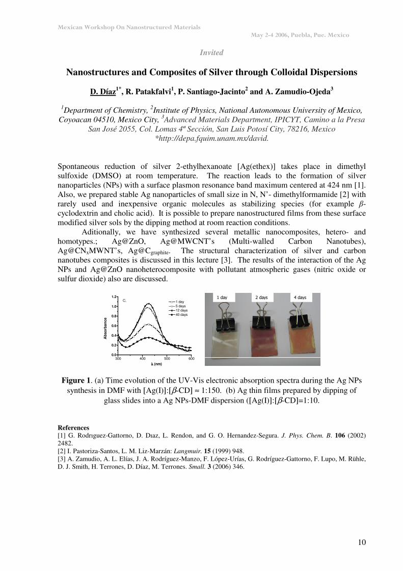
Spontaneous reduction of silver 2-ethylhexanoate [Ag(ethex)] takes place in dimethyl sulfoxide (DMSO) at room temperature. The reaction leads to the formation of silver nanoparticles (NPs) with a surface plasmon resonance band maximum centered at 424 nm [1]. Also, we prepared stable Ag nanoparticles of small size in N, N’- dimethylformamide [2] with rarely used and inexpensive organic molecules as stabilizing species (for example �-cyclodextrin and cholic acid). It is possible to prepare nanostructured films from these surface modified silver sols by the dipping method at room reaction conditions.
Aditionally, we have synthesized several metallic nanocomposites, hetero- and homotypes.; Ag@ZnO, Ag@MWCNT’s (Multi-walled Carbon Nanotubes), Ag@CNxMWNT’s, Ag@Cgraphite. The structural characterization of silver and carbon nanotubes composites is discussed in this lecture [3]. The results of the interaction of the Ag NPs and Ag@ZnO nanoheterocomposite with pollutant atmospheric gases (nitric oxide or sulfur dioxide) also are discussed.
300 400 500 6000.0
0.2
0.4
0.6
0.8
1.0
1.2
Abs
orba
nce
λλλλ (nm)
1 day 5 days 12 days 40 days
C,
������ ������� �������
Figure 1. (a) Time evolution of the UV-Vis electronic absorption spectra during the Ag NPs synthesis in DMF with [Ag(I)]:[β-CD] ≈ 1:150. (b) Ag thin films prepared by dipping of
glass slides into a Ag NPs-DMF dispersion ([Ag(I)]:[β-CD]=1:10. References [1] G. Rodrıguez-Gattorno, D. Dıaz, L. Rendon, and G. O. Hernandez-Segura. J. Phys. Chem. B. 106 (2002) 2482. [2] I. Pastoriza-Santos, L. M. Liz-Marzán: Langmuir. 15 (1999) 948. [3] A. Zamudio, A. L. Elías, J. A. Rodríguez-Manzo, F. López-Urías, G. Rodríguez-Gattorno, F. Lupo, M. Rühle, D. J. Smith, H. Terrones, D. Díaz, M. Terrones. Small. 3 (2006) 346.
���������� ��������� ������������������ �� ��������������������������������������������������������������������������������������������������������������������������������������������������������
11
Invited
Photonics Properties of Rare-Earth Doped ZrO2 Nanocrystals
Dr. Elder De la Rosa
Centro de Investigaciones en Óptica, Leon, México E-mail: [email protected]
In the last years, nanocrystalline ZrO2 doped with different rare earth ions have been prepared by sol-gel process and the optical properties were studied. It has been demonstrated that dopants ions control the crystalline structure of ZrO2 in combination with the annealing temperature. Metastable tetragonal phase was obtained for samples annealed at 500oC and monoclinic for samples annealed at 1000oC. However, the presence of rare earth stabilizes tetragonal phase at 1000oC, but for high concentration of dopant cubic crystalline structure was obtained. Optical properties depend on the crystalline structure. The thermoluminescence characterization of nanophosphor shows a strong peak at 130oC and 400oC for monoclinic and tetragonal structure, respectively. Results show a good potential of this nanophoshor for dosimetry applications of γ-, β-, and X-ray; furthermore, it has been shown that this is the only dosimeter that cover all the UV spectra. Doping with the appropriate ion it was obtained visible emission pumping with a UV source opening the potential application in solid state lighting and displays. Strong visible emission was also obtained pumping with a near infrared source that suggests good potential for application such as security, biomedicine, displays, and lasers.

���������� ��������� ������������������ �� ��������������������������������������������������������������������������������������������������������������������������������������������������������
12
Invited
Trends in the Structural Properties of Gold Nanoclusters
Dr. Ignacio L. Garzón Instituto de Física, Universidad Nacional Autónoma de México, México D.F. 04510, México.
E-mail: [email protected] The physical and chemical properties of small coinage metal clusters, with atomic structures nd10(n+1)s1 (n = 3,4,5 for Cu, Ag and Au, respectively), are of great interest since, for example, can be viewed as a bridge between those existing in the "simple" s-only alkali metal and the more complicated transition metal clusters. In particular, gold clusters have attracted a lot of attention due to the possible existence of special geometrical structures corresponding to stable minima of the potential energy surface [1].
In fact, several theoretical calculations and indirect experimental evidence have shown that AuN clusters prefer planar structures up to sizes around N=13, cage-like structures for the Td Au20 and Ih Au32 [2], and low-symmetry (amorphous) configurations for Au55 [3]. On the other hand, there has been important experimental progress on the structural characterization of size selected clusters, using for example, electron diffraction on trapped ion metal clusters [4] and photoelectron spectroscopy [5].
In this work, we present a theoretical study of the structural and electronic properties of Au neutral, cationic and anionic clusters with up to N=55 atoms, using density functional theory in the generalized gradient approximation. The trends in the structural and electronic properties of the Au clusters are discussed in terms of the strong relativistic effects present in them. An interesting result coming out from these calculations indicates that not only the size (number of atoms) and shape (isomer geometry) of a given cluster determine its properties, but also the charge present in the system may affect the cluster behavior even in the larger sizes with N=55. A discussion of the structural motifs existing in neutral, cationic and anionic Au clusters with up to N=55 atoms and their connection with recent experimental data will be presented. In particular, theoretical evidence on the existence of chiral gold clusters [6], and their relevance in connection with enantioselectivity properties will be discussed. References [1] I.L. Garzón, K. Michaelian, M.R. Beltran, A. Posada-Amarillas, P. Ordejon, E. Artacho, D. Sanchez-Portal, and J.M. Soler, Phys. Rev. Lett. 81 (1998) 1600. [2] E.M. Fernández, J.M. Soler, I.L. Garzón, and L.C. Balbás, Phys. Rev. B 70 (2004) 165403. [3] J.M. Soler, M.R. Beltran, K. Michaelian, I.L. Garzón, P. Ordejon, D. Sanchez-Portal, and E. Artacho, Phys. Rev. B 61 (2000) 5711. [4] X. Xing, R.M. Danell, I.L. Garzón, K. Michaelian, M.N. Blom, M.M. Burns, and J.H. Parks, Phys. Rev. B 72 (2005) 081405(R). [5] H. Häkkinen, M. Moseler, O. Kostko, N. Morgner, M.A. Hoffmann, and B. v. Issendorff, Phys. Rev. Lett. 93 (2004) 093401. [6] I.L. Garzón, M.R. Beltrán, G. González, I. Gutiérrez-González, K. Michaelian, J.A. Reyes-Nava, and J.I. Rodríguez-Hernández, Phys. Rev. B 66 (2002) 073403.
���������� ��������� ������������������ �� ��������������������������������������������������������������������������������������������������������������������������������������������������������
13
Invited
Nanostructured Carbon: Theory and Experiment
Prof. Dr. Humberto Terrones
Head of Advanced Materials Department, IPICYT, Camino a la Presa San José 2055, Col. Lomas 4. Sección, San Luis Potosí 70216, México, Tel: (52) 444 834 20 39; Fax: (52) 444 834
20 40. E-mail: [email protected] Graphite has proved to be very flexible forming not only fullerenes and nanotubes, but other more complicated arrangements such as onion-like structures, cones, coalesced fullerenes inside single walled nanotubes (peapods), coalesced tubes, junctions, etc. Graphite is just one example, there are layered compounds such as boron nitride and metal dichalcogenides which also exhibit curved nanostructures. In this account it is shown that there are several possibilities of new hypothetical layered nanostructures, with amazing properties, waiting to be discovered. In addition, growth mechanisms and self assembly of new layered architectures are analyzed. Understanding the growth and form of layered compounds will allow us to make a substantial contribution in future nanotechnological applications.
���������� ��������� ������������������ �� ��������������������������������������������������������������������������������������������������������������������������������������������������������
14
Invited
Nanotechnology Applied to Renewable Energy Generation, Storage and Application
P.J. Sebastián1,2, S.A. Gamboa1, X. Mathew1, J. Pantoja2 and J. Moreira2
1Centro de Investigación en Energía-UNAM, Temixco, Morelos 62580 2Universidad Politecnica de Chiapas, Tuxtla Gutiérrez, Chiapas 29010
Nanotechnology has lately assumed a special role in different areas of science, technology and medicine. In the technology area special mention may be given to the renewable energy area. Like nanotechnology, renewable energy technologies have also gained importance during the past few years. Both these technologies involve a certain level of sophistication in their development and application and hence at present they are not cost effective. The research and development on these technologies are oriented towards lowering cost, new techniques and processes, new materials etc. The interdependence between nanotechnology and renewable energy technologies have become more relevant in this context. In this work we will be presenting the latest developments in renewable energy technologies where nanotechnology is applied as a tool their generation, storage and application. In particular, special mention will be given to renewable energy technologies like solar, hydrogen, fuel cells and energy storage devices. Electrical energy generation and clean fuel production based on renewable technologies will be treated. Energy and fuel storage where the importance of nanotechnology will be discussed. Application of renewable energy devices and sources in nanotechnology will be presented. Recent results obtained in all these areas in our group will be presented and discussed.
���������� ��������� ������������������ �� ��������������������������������������������������������������������������������������������������������������������������������������������������������
15
O001
Melting and Freezing of Au-Pd Nanoparticles
Sergio J. Mejía-Rosales*, Carlos Fernández-Navarro, Eduardo Pérez-Tijerina
Facultad de Ciencias Físico-Matemáticas, Universidad Autónoma de Nuevo León, San Nicolás de los Garza, Nuevo León, México 66450, Tel.: 8183294030, Fax: 8183522954
E-mail: [email protected]
Juan M. Montejano-Carrizales
Instituto de Física, Universidad Autónoma de San Luis Potosí, San Luis Potosí, S.L.P., México 78000
Miguel José-Yacamán
Chemical Engineering Department and Texas Advanced Materials Center, The University of
Texas at Austin, Austin Texas 78712, USA In this work we study the structure details and dynamic behavior of AuPd 923-atom nanoparticles, for the specific case of icosahedral geometry, using Molecular Dynamics (MD) techniques in the canonical ensemble. We observe that the melting transition temperature of each cluster depends on the relative concentration of gold and palladium, and that hysteresis is present in the heating-cooling process. After melting of the outer shell, gold atoms migrate to the surface; this rearrangement may be of particular relevance in the chemical activity of the particle. In the cooling series, we study the structures by the analysis of the bond-order parameter, finding that the structures obtained by freezing the particles are formed by either alternating layers of HCP and FCC atoms, or by FCC regions delimited by monolayers of HCP atoms, depending on the amount of Pd present on the particle. Apparently this is not the case for the monometallic particles that tend to form icosahedra. This kind of structuring in small nanoparticles may be related with the rich schema of geometries observed by TEM in Au-Pd nanostructures.
���������� ��������� ������������������ �� ��������������������������������������������������������������������������������������������������������������������������������������������������������
16
O002
Attachment of Gold Nanoparticles to Thiol-Functionalized Multi-walled Carbon Nanotubes
Rodolfo Zanella1*, Elena V. Basiuk1, Patricia Santiago2, Vladimir A. Basiuk3, Edgar
Mireles1, and José M. Saniger1
1CCADET, UNAM, Circuito Exterior, C. U., A. P. 70-186, C.P. 04510 México D.F., Mexico.
2Instituto de Física, UNAM, Circuito de la Investigación Científica, C. U., 04510 3Instituto de Ciencias Nucleares, UNAM, Circuito Exterior, C.U., 04510
Fax: 56 22 86 51. E-mail: [email protected] The attachment of metal nanoparticles to carbon nanotubes (CNTs) is a way to obtain new hybrid materials with useful properties for gas sensor and catalytic application and could also serve to detect the presence of certain functional groups on their surfaces. There are some reports of successful supporting of gold on CNTs1-3. In most of these reports a special attention is dedicated to get an adequate preliminary treatment of CNT supports. Since CNTs are chemically inert, activating their surface is an essential prerequisite for linking the metal nanoclusters to them.
In the present work we developed a direct solvent-free functionalization of pristine multiwall nanotubes (MWNT) with aliphatic bifunctional thiols (2-aminoethanethiol and 1,6-hexanedithiol), aimed to the preparation of chemically modified nanotube surfaces capable of binding gold nanoparticles. Small gold particles (1.7 nm) with narrow particle size distribution were obtained for MWNTs functionalization with 1,6-hexanedithiol. For MWNTs functionalized with aminothiol the average particle size was greater (5.5 nm). This difference in particle size is explained by a coalescence phenomenon of gold particles in aminothiol functionalized sample. The interaction between gold nanoparticles and functionalized nanotubes is strong enough to avoid the nanoparticle loss even when the samples were thoroughly washed. Gatan Image Filter observations show that sulfur is covering most of the nanotube surface with a no homogeneous distribution. A higher sulfur concentration was observed around the gold nanoparticles location. References [1] Fasi, A.; Palinko, I.; Seo, J. W.; Konya, Z.; Hernadi, K.; Kiricsi, I. Chem. Phys. Lett. 372 (2003) 848. [2] Jiang, K.; Eitan, A.; Schadler, L. S.; Ajayan, P. M.; Siegel, R. W.; Grober, N.; Mayne, M.; Reyes-Reyes, M.; Terrones, H.; Terrones, M. Nano Lett. 3 (2003) 275. [3] Jiang, L.; Gao, L. Carbon 41 (2003) 2923.
���������� ��������� ������������������ �� ��������������������������������������������������������������������������������������������������������������������������������������������������������
17
O003
Optical and HRTEM Characterization of Metallic Nanoparticles Produced by MeV Ion Implantation
J.C. Cheang-Wong, A. Oliver, L. Rodríguez-Fernández, A. Crespo-Sosa, and J. Arenas
Instituto de Física, Universidad Nacional Autónoma de México. A.P. 20-364, México, D.F.
01000, México, Fax: (52)-55-56 22 50 09. Email: [email protected]
Ion implantation has attracted considerable interest as a method to modify the optical properties of insulators in order to produce materials with nonlinear optical properties. In this work we describe the synthesis of metallic nanoparticles in silica by MeV ion implantation using the IFUNAM´s Pelletron accelerator. Several factors such as the ion fluence, the radiation damage induced by the ion implantation, and the subsequent thermal annealing conditions (temperature, atmosphere, etc.) can determine the shape, size and distribution of the clusters in the sample. High-purity silica samples were implanted at room temperature with Cu, Ag or Au ions at various fluences up to 6×10¹⁶ ions/cm2. The samples were then annealed in either a reducing or an oxidizing atmosphere at temperatures ranging from 300ºC to 1100ºC. The samples were characterized by optical absorption and HRTEM. Rutherford Backscattering Spectrometry was used to determine the concentration of the implanted ions and their depth distributions in the samples. Changes in the optical properties of the samples arise from nanometer-sized metallic clusters produced as a result of implantation and/or annealing. The metallic nanoclusters strongly absorb optical radiation at the surface plasmon resonance wavelength (~560 nm for Cu, ~400 nm for Ag, and ~520 nm for Au). Reducing and oxidizing annealing atmospheres affect in a different way the nucleation and growth of Cu, Ag and Au nanoparticles. The implications and the possible mechanisms concerning this behavior are discussed in this paper.
���������� ��������� ������������������ �� ��������������������������������������������������������������������������������������������������������������������������������������������������������
18
O004
Structural and Thermodynamical Properties of Nanoalloy Clusters
José Luis Rodríguez López, and Juan Andrés Reyes Nava
Advanced Materials Department, IPICYT
Instituto Potosino de Investigación Científica y Tecnológica, A.C. Camino Presa San José 2055, Lomas 4a, San Luis Potosí, SLP, México.
E-mail: [email protected], [email protected] Extensive molecular dynamics simulations on metallic nanoalloyed clusters of PdPt, AuPt, and PtNi have been performed. Three different concentrations were built on cluster sizes of 561 and 923 atoms. From the structural results for PdPt, we have found that these systems have the tendency to uniformly been alloyed all along the cluster, contrasting with some other systems that present the core-shell structure, like AuPt, NiPt alloy clusters.
We also present and discuss dynamic and thermodynamical properties like Lindemann parameter (rms bond length fluctuation) and atomic diffusive coefficients, caloric curves, heat capacities, and melting temperatures for all these systems.
���������� ��������� ������������������ �� ��������������������������������������������������������������������������������������������������������������������������������������������������������
19
O005
Nanostructure Formation in Al-Sn-Alloys by Severe Plastic Deformation
R. Schouwenaars, A. Bravo, J.A. Torres, A. Ortiz, and V.H. Jacobo Department of mechanical engineering, DIMEI, National Autonomous University of Mexico,
Avenida Universidad 3000, Coyoacán, D.F. C.P. 04510, México. Fax: 55 56 80 58 E-Mail: [email protected]
Al-Sn-alloys have been used in tribological applications for more than fifty years. As the operation conditions in combustion engines are becoming more severe, fundamental understanding on wear mechanisms in these alloys is needed and novel processing paths must be explored. The paper resumes results by the authors showing that wear in ductile triboalloys is accompanied by severe plastic deformation (SPD) and the generation of a nanoscale structure containing unstable and metastable phases. Comparing these findings to literature relating to tribolayer formation in other alloy systems, good agreement with the result of other research groups is found. Based on the former, SPD was also proposed as a viable way for obtaining nanostructured, ductile Al-Sn alloys for tribological applications with increased resistance, as is supported by extensive literature related to the generation of nanostructures in other Al-alloys by SPD. While for most metals SPD requires low-volume, high cost processes, aluminium can be cold rolled to extreme reductions. Once conventional rolling is exhausted, accumulated roll bonding (ARB) can be applied. Material properties and microstructures measured after severe cold rolling show that while the Al-structure is refined to nanoscale, the Sn-phase is reduced to such dimensions that it reaches its theoretical tensile strength (�E/10) and fractures at this stress during rolling and tensile testing. Comparing the results of conventional rolling to the ones obtained after ARB, it is found that the additional shear component induced by ARB produces a morphology which differs significantly from the former, indicating that further microstructural refinement is possible through this route.
���������� ��������� ������������������ �� ��������������������������������������������������������������������������������������������������������������������������������������������������������
20
O006
Synthesis and Characterization of Cu Nanoparticles Thin Films and Powders
Miguel Ángel Gracia Pinilla, Luis Gerardo Silva Vidaurri, Sergio J. Mejía-Rosales,
Eduardo Pérez-Tijerina
Laboratorio de Nanociencias y Nanotecnología, Facultad de Ciencias Físico-Matemáticas, Universidad Autónoma de Nuevo León, San Nicolás de los Garza, Nuevo León, México
66450. Phone: 8183294030, Fax: 8183522954. E-mail: [email protected]
Miguel José-Yacamán Chemical Engineering Department and Texas Advanced Materials Center, The University of
Texas at Austin, Austin Texas 78712, USA In the present work we study the synthesis of Cu nanoparticles, their structural, morphological and chemical characterization, as well as their optical properties, by the use of the techniques of X-ray diffraction (XRD), scanning electron microscopy (SEM), transmission electron microscopy of (TEM), atomic force microscopy (AFM), scanning auger microscopy (SAM), and UV-visible spectroscopy. The Cu nanoparticles are produced by magnetron sputtering followed by thermalization and condensation in high pressure zones. The size of nanoparticles is controlled through the handling of three variables, flow of gases (Ar and there He), power (Watts) and aggregation zone length. Typically nanoparticles may be generated and measured with diameters ranging from ~0.7nm to 20nm in diameter. If the quadrupole is not inline then the particle diameter distribution is around ±20%. If the quadrupole is inline, then the distribution can be reduced to around ±2%.
The synthesized nanoparticles were obtained in thin films and powders, as main characteristic their size, which is located within the range of 1-10nm, the spectrum of absorption shows a shift related the effect of the shape of the nanoparticles. ___________________________________________________________________________ Acknowledgment: This work was supported by the Council for Science and Technology of the State of Nuevo León.

���������� ��������� ������������������ �� ��������������������������������������������������������������������������������������������������������������������������������������������������������
21
O007
What Factors Determine the Core-Shell Structure on Binary Alloy Clusters?
Juan Andrés Reyes Nava1 and José Luis Rodríguez López2
Advanced Materials Department, Instituto Potosino de Investigación Científica y Tecnológica,
Camino Presa San José 2055, Lomas 4a, San Luis Potosí, SLP, México E-mail: [email protected], [email protected]
Lowest energy structures of Au-Pt, Pt-Ni and Pt-Pd nanoalloys with size of 561 atoms were found. Numerical simulations of the slow freezing of these binary systems A-B at the concentrations A1B3, A1B1, y A3B1 from high temperature liquid phase show a core-shell structure in Au-Pt and Pt-Ni, and mixing alloying in the case of Pt-Pd. These different atomic species distributions are explained on the basis of the atomic properties at the level of the many body inter-atomic potential used.
���������� ��������� ������������������ �� ��������������������������������������������������������������������������������������������������������������������������������������������������������
22
O008
Microstructure in Hybrid Block Copolymer-Inorganic Nanocomposites
Angel Romo-Uribe Laboratorio de Nanopolimeros, Centro de Ciencias Físicas – UNAM, Cuernavaca, Morelos,
C.P. 62210, Mexico. Tel / Fax: 777-329 0880 E-mail: [email protected]
The morphology of a series of block copolymer-inorganic nanocomposites was characterized using small-angle X-ray scattering (SAXS). The copolymers are of the A-B type, where A corresponds to blocks of poly(isoprene) -PI- and B corresponds to blocks of poly(ethylene oxide)-PEO. The inorganic material consists of a crosslinked sol of 3-glycidoxypropyltrimethoxysilane and aluminum-tri-sec-butoxide in a 4:1 mole ratio, to generate an aluminosilicate ceramic. Two series of block copolymers, designated PI-b-PEO-D and PI-b-PEO-E were studied; these correspond to 15 wt% PEO and 13 wt% PEO, respectively. For each series of composites the concentration of inorganic component was varied. The results showed that the nanoscale order characteristic of block copolymers is preserved in these hybrid nanocomposites. The amount of inorganic material and the molecular weight of the blocks determine the nature of the morphology. Moreover, SAXS enables to determine whether the microphases are separated by either sharp or diffuse boundaries.
���������� ��������� ������������������ �� ��������������������������������������������������������������������������������������������������������������������������������������������������������
23
O009
Frequency Spectrum and Confinement of Nanorods Radiation in Multilayered Nanosphere
Gennadiy N. Burlak and Alfredo M. Chavez
Centro de Investigación en Ingeniería y Ciencias Aplicadas, UAEM, Cuernavaca, Mor.
México. Fax: 777+3297084 E-mail: [email protected]
Recent years, the techniques of using radiated nanostructures in nano- and micro-spheres have provided a new view of various effects and interactions in structured nanolayered media. It is well known that a dielectric nanosphere has a complex spectrum of the electromagnetic low quality factor eigen oscillations because of a leakage into the outer space. The case of a compound structure: the dielectric sphere coated by an alternative stack is more various. In this report, we study the frequency spectrum and the spatial dependences of electromagnetic field radiated by quantum semiconductor nanorods attached or impregnated into multilayered microsphere. We found, that even in a dissipative case the frequency spectrum consists of the series of narrow and well separated frequency peaks. In area of such resonances the spherical structure confines the field of nanorods. In result the field’s oscillations become deeply located in the coated microsphere and practically do not leave to a surrounding space. We found the possibility generation of coupled photon states by two nanorods assisted by a presence of the alternating spherical stack. Since the width of resonant peaks is rather small, it allows creating highly polarized nanoemitters oscillating with very high quality factor to actively control the polarization state of microcavity photons. Taking into account the weak random deviations in thickness of spherical layers does not change this conclusion. Engineering methods of attaching such nanostructures to the surface or interfaces of coated microspheres can open new opportunities for active control of arrays of the light nanoemitters. Such states can be useful not only for the operational purposes, but also for quantum information technologies.
���������� ��������� ������������������ �� ��������������������������������������������������������������������������������������������������������������������������������������������������������
24
O010 Design of Hybrid Materials Based on Carbon Nanotubes or Nanofibers and
Polyoxometalates, and their Application in Electrochemical Supercapacitors
A. Karina Cuentas-Gallegos, R. Martínez-Rosales, M. González-Toledo, and M. E.
Rincón
Centro de Investigación en Energía-UNAM, Priv. Xoxhicalco S/N, Col. Centro, Temixco, Mor., México. Fax +52-55-5622974
E-mail: [email protected] The focus of our work was the design of novel hybrid materials based on carbon nanotubes (MWCNT) or nanofibers (NFC), and polyoxometalates (POM). These nanocomposites were carried out by POM adhesion onto previously functionalized nanocarbon surface, in order to use POM as nanotube/nanofiber dispersor, and as energy storage enhancer in supercapacitor cells [1, 2]. We carried out the characterization of these materials by FTIR, XRD, SEM, and TEM. Surprisingly, TEM analyses showed that in some cases particles could penetrate into MWCNT. Finally, we assembled symmetrical supercapacitive solid-state cells, where the cyclability was very good at high cycling rates (I=1000mA/g) for MWCNT/POM during 500 charge-discharge cycles, with good capacitance values of ≈35 F/g. From material science point of view these materials are innovative, and open the way to search for diverse applications, such as, sensors, catalyzers, photovoltaic cells, energy storage, etc.
���������� ��������� ������������������ �� ��������������������������������������������������������������������������������������������������������������������������������������������������������
25
O011
Cathodoluminescence Study of ZnO:In Nanowires
A. González Carrazco 1, M. Herrera Zaldívar1, J. Valenzuela Benavides1, A. Escobedo Morales2, and U. Pal2
1Centro de Ciencias de la Materia Condensada, Universidad Nacional Autónoma de México, Apdo. Posta 2681, Ensenada, BC 22800, México
2Instituto de Física, Universidad Autónoma de Puebla, Apdo. Postal J-48, Puebla, Pue. 72570, México
E-mail: [email protected]
ZnO nanowires grown by the hydrothermal method and doped with In of different concentrations have been characterized by cathodoluminiscence. A shift of the near band edge peak towards lower energies is observed in spectra obtained for the nanostructures. This behaviour some times related to the presence of dislocations or point defects is studied by means of monochromatic catodoluminescence images acquired at different temperatures. The typical broad green emission of the ZnO is observed in the spectra, which present two components centred around 2.3 and 2.0 eV with heights dependent of the In concentration. An emission centred at 1.87 eV is also observed in the samples, attributed to the presence of impurities.
���������� ��������� ������������������ �� ��������������������������������������������������������������������������������������������������������������������������������������������������������
26
O012
Formation of SiOx Nano-Films at Laser Ablation of Si and Composite SiC-Ceramic
P. A. Marquez Aguilara, M. Vlasova, M. C., Reséndiz-González, M. Kakazey and I.
González Morales
The Autonomous University of the State of Morelos, Av. Universidad, 1001, Cuernavaca, Mexico. E-mail: [email protected]
By methods of electron microscopy, atomic force microscopy, X-ray microanalysis, optical transmission spectroscopy the influence of IR laser irradiation in continuous regime (λ = 1064 nm, P = 240 mW, 175 W and 210 W) on Si and SiC-CrSi3 ceramics is investigated.
It is established that the basic product of ablative is silicon. Depending on capacity of radiation, time of an irradiation and composition of the gas environment on a surface of a quartz substrate films of SiOx and SiOx:N, where x ≤ 2 are precipitated. At various stages of an irradiation (from a mode of evaporation up to laser plasma formation) nano-films of various morphologies are formed. As well as at a pulse irradiation, laser plasma is an effective source of formation of fractal nano-dimension structures.
���������� ��������� ������������������ �� ��������������������������������������������������������������������������������������������������������������������������������������������������������
27
O013
Characterization of Silica Nanoparticles for Hybrid Coatings with Enhanced Optical Porperties
Calderón-Guillén J.1,2, Avilés-Arellano L.M.1, Pérez-Robles J.F.1, Almaral-Sánchez J.L.2,
and González-Hernández J.1
1Centro de Investigación y Estudios avanzados del Inst. Politéc. Nal., Unidad Querétaro Libramiento Norponiente # 2000. Frac. Real de Juriquilla. Santiago de Querétaro, Qro. 2Universidad Autónoma de Sinaloa, Ángel Flores y Riva Palacio s/n, Col, Centro, C.P.
81010, Culiacán Sinaloa, México. E-mail: [email protected]. The organic-inorganic hybrid materials have an enormous potential application, because unfavorable properties of the part can be improved by the properties by means of the properties of the other one [1-5].
The Hybrid materials have many applications; some of them are coatings in general coatings on acrylic materials where it is required to increase the abrasion properties. In the same way the introduction of silica in a polymeric material can be made and used to build different products like bathroom tubs, washes hands, car windshield, domes, etc. [1, 2].
The aim of this work is to obtain SiO2 nanoparticles with a controlled size, and introduce them in a polymer matrix and deposited on different substrates (for instance acrylic substrate) for improving their optical and mechanical properties. In addition, the introduction of metal oxide particles inside a polymer matrix increases the coating appearance.
Hybrid suspensions were made by using silica, prepared by the acid sol-gel process, and Poly Methyl MethAcrylate (PMMA). Silica was prepared using 40% mol of water and hybrid materials were prepared using 20, 50, and 80 percent by weight of polymer. In silica suspensions were made measurements of size and zeta potential using the NanoSizer ZS and AcoustoSizer II equipments respectively. The particle size in silica suspensions aged 10 days of was about 10 nm for the hybrid suspensions (20, 50, and 80% w/w of polymer), and the zeta potential changed with the polymer/silica ratio. Hybrid coatings were obtained on glass and acrylic substrates by dip coating. These coatings were treated at 70°C for 2h and later at 100°C for 1h.
Optical studies of Reflection-Transmittion (R-T) showed that the hybrid coatings were homogeneous and had different thickness: 450, 360, and 220 nm for 20, 50, and 80 % W of the monomer, MMA. Also their transparence was increased more than 2 % when compared with the target material. The presence of silica particles increased the optical properties of hybrid coatings, and these properties were independent of the polymer/SiO2 ratio. References [1] Wei Y, Bakthavatchalam R, Yang DC, and Whitecar CK. Polym Prepr 32 (1991) 503. [2] Wei Y, Yang DC, and Bakthavatchalam R. Mater Left 3 (1992) 261. [3] Wei Y, Yang DC, Tang LG, and Hutchins MK. J Master Res. 8 (1993) 1143. [4] Wei Y, Yang DC, Tang LG, and Macromol Chem Rapid Común. 14 (1993) 273. [5] Novak BM and Davis C. Macromolecules 24 (1991) 5481.
���������� ��������� ������������������ �� ��������������������������������������������������������������������������������������������������������������������������������������������������������
28
O014
Ensanchamiento de Bandas Prohibidas en Cristales Fotónicos en Dos Dimensiones por Medio de Heteroestructuras
Jesús Manzanares-Martinez, Raúl Garibay-Alonso, Diego Soto-Puebla y Raúl
Archuleta-García
Departamento de Investigación en Física, Universidad de Sonora E-mail: [email protected]
Demostramos teóricamente que la banda fotónica pohibida omnidireccional de una estructura fotónica en dos dimensiones se puede ensanchar por medio de heteroestructuras, la cual consiste en la unión de dos diferentes cristales fotónicos bidimensionales seleccionados de manera que sus respectivas bandas prohibidas se superpongan. La existencia de la banda fotónica completa de la estructura híbrida se confirma proyectando la banda fotónica y por cálculos de la transmisión.
���������� ��������� ������������������ �� ��������������������������������������������������������������������������������������������������������������������������������������������������������
29
O015
Propagación de Ondas Electromagnéticas en Estructuras Cuasi-uno-dimensionales Tipo Peine
Gregorio H. Cocoletzi1,2, L. Dobrzynski2, B. Djafari-Rouhani2, H. Al-Wahsh2,3, D. Bria2,4
1Instituto de Física, Universidad Autónoma de Puebla, Apartado Postal J-48, Puebla, 72570
Puebla, México. E-mail: [email protected] 2Institut d’Electronique, de Microelectronique et de Nanotechnologie (IEMN), UMR CNRS
8520, Université des Sciences et Technologies de Lille, 59655 Villeneuve d’Ascq Cédex, France.
3 Faculty of Engineering, Benha University, 11241 Cairo, Egypt 4 Faculté des Sciences, Université Mohamed I, 60000 Oujda, Morocco
Estudiamos la propagación de ondas electromagnéticas en líneas infinitas (guías de onda) sobre las cuales se conectan líneas finitas (resonadores) en dirección perpendicular para formar estructuras tipo peine. Las guías de onda y los resonadores se representan mediante la función dieléctrica )(ωε y permeabilidad magnética )(ωµ las cuales dependen de la frecuencia de la radiación electromagnética. Nuestros estudios se centran en la región de frecuencia donde los resonadores tienen índice de refracción negativo, es decir, )(ωε y )(ωµ son ambos negativos, que dan lugar a velocidad de fase negativo. Para estudiar las propiedades ópticas, usamos el método de la función de Green. Iniciamos los estudios considerando la guía de onda teniendo un solo resonador. Para esta estructura calculamos la transmisión de la radiación electromagnética. Después variamos el número de resonadores y estudiamos la transmisión y la estructura de bandas. La transmisión para un solo resonador despliega mínimos los cuales se interpretan en términos de resonancias. Estos mínimos se convierten en brechas prohibidas para la propagación de ondas cuando se tiene una estructura periódica de resonadores. Las relaciones de dispersión de los modos colectivos para sistemas periódicos muestran estructuras de bandas permitidas y brechas prohibidas para la propagación de ondas electromagnéticas, los cuales dependen del tamaño de los resonadores, de la separación entres ellos y de )(ωε y )(ωµ . En la última parte de los estudios, mostramos los efectos de la disipación en la estructura de la transmisión. ___________________________________________________________________________ Agradecimientos. El trabajo ha sido apoyado por: SEP-PROADU 2003-01-21-001-051, y CONACYT-BUAP Project # II010G02. También por “le Fonds Européen de Développement Régional” (FEDER) y “ Le Conseil Régional Nord-Pas de Calais”.
���������� ��������� ������������������ �� ��������������������������������������������������������������������������������������������������������������������������������������������������������
30
O016
Microstructural Characterization of Co3O4 Nanoparticles Produced by Mechanochemical Reactions
1G. García-Pacheco and 2J.G. Cabañas Moreno
1 IPN, ESFM, UPALM, Edif. 9, Zacatenco, 07300, México D.F.
2 IPN, ESIME, UPALM, Academia de Física, ICE, Zacatenco, 07338, México D.F. E-mail: [email protected]
The refinement of the microstructure in the materials at nanometric levels has allowed observing “unusual” behaviours of its macroscopic properties; which, have as well allowed to the development of new applications and/or greater commercials products benefit. Thus, significant advances have been made in the production of nanocrystalline materials through the use of a variety of physical and chemical processes. The cobalt oxides have been chosen because of the small number of possible equilibrium oxides; thus avoiding the need to characterize a complex mixture of oxides. The oxides of cobalt (CoO and Co3O4) constitute a range of important technological applications, such as, catalyst, sensors and magnetic recording media.
The literature reports a number of techniques to produced nanoparticles of Co3O4 phase; however, the processes require a strict control of many variables and may also be followed by elaborated post-treatment to obtain the Co3O4 phase. The goal of this investigation is to explore a simple route to prepare sizable amounts of cobalt oxide nanoparticles by chemical reactions mechanically induced. The initially proposed reaction was:
Milling CoCO3 + Na2O → CoO + Na2CO3
In agreement with this reaction, the product was constituted by oxide of interest
dispersed on a matrix of Na2CO3, which could be removed by means of a process of washing. The techniques of X Ray Diffraction (XRD), Volumetric Chemical Analysis (VCA), Scan Electron Microscopy (SEM) and Transmission Electron Microscopy (TEM) were used to characterize the as-milled and washed powders. The images obtained by SEM and TEM showed nanoparticles, whose average size was less than 50 nm. Such nanoparticles were forming smooth agglomerate of irregular form and sizes (< 1 µm- 50 µm). The XRD results showed that the reaction carried out on stable and gradual way. Additionally, the Co3O4 phase was detected at 24h of milling. Through of XRD and VCA results indicated that formation of this phase occurred by the decomposition of Na2CO3 phase during milling, according this reaction:
Milling 3CoO + Na2CO3 → Co3O4 + CO2 + 2Na
���������� ��������� ������������������ �� ��������������������������������������������������������������������������������������������������������������������������������������������������������
31
O017
Structural, Optical and Electric Properties of Nanostructured SnO2:F Films Deposited by Pulsed Spray Pyrolysis
Dwight R. Acosta and Jesús M. Ortega
Instituto de Física, UNAM, México D.F.
E-mail: [email protected], [email protected] SnO2:F is a transparent conductive oxide that in thin film configuration is used as substrate, superstrate or as transparent electrode in solar and electrochromic devices. The control and improve of physical properties of this semiconductor oxide must contribute to the improvement of efficiency and to low the cost of opto-electonic devices. The pulsed spray pyrolysis let a better control of the substrate temperature in thin film deposition processes and has been used in this work to deposit SnO2:F films varying the SnCl4/NH4F ratio in order to produce and induce stoichiometric changes in the material than in turn might favor the charge transport in electrochromic phenomena, for instance. For all the films deposited on glass substrate, polycrystalline and nanostructured materials were detected from X- ray diffraction and from scanning and atomic force observations respectively. The optical properties were studied by spectrophotometry in the UV and visible range of the spectra and interesting variations in the band gap of SnO2:F materials from 4.25 to 4.32 eV were found using the Moss Burstein approximation for thin films. The films prepared for low SnCl4/NH4F ratios showed an increase in the surface resistivity values. The variations found in optical and electrical properties have been correlated with the synthesis parameters and also with structural and morphological details observed in scanning and atomic force micrographs. The correlation between band gap energy Eg, conductivity and grains size is explored and presented in this work. The films obtained referred in the title of this work were used as substrate for deposition of WO3 thin films by spray pyrolysis and the influence of SnO2:F physical properties just mentioned in the electrical and optical of the nanostructured WO3/ SnO2 system is also presented in this work.
���������� ��������� ������������������ �� ��������������������������������������������������������������������������������������������������������������������������������������������������������
32
O018
ab initio Study of the Structural and Electronic Properties of SnO Nanotubes
Fernando Alvarez-Ramirez and Yosadara Ruiz-Morales
Programa de Ingeniería Molecular, Instituto Mexicano del Petróleo, Eje Central Lázaro
Cárdenas 152, México D.F. 07730, México.Tel. (52 55) 9175-8424, Fax. (52- 55) 175-6239. E-mail: [email protected], [email protected]
Structural and electronic properties of single wall nanotubes of SnO2 are studied on the basis of DFT calculations using the Density Functional Theory (DFT) with the functional of Perdew and Wang (GGA-P91). The structural models were built with periodic boundary conditions along the nanotube axis and in two main configurations: armchair and zigzag. The structural and electronic chiral effects were analyzed on six configurations keeping fix the number of crystalline units, Nu=12, varying the chiral angle from a zigzag to a armchair. The band gap shows an increment behavior as function of the nanotube radios both cases zigzag (2.55 eV to 2.85 eV) and armchair (2.0 eV to 2.75 eV). The Mulliken and Hirshfeld charge analysis in all the cases do not present significant changes. Finally, an analysis of density of states and their correlation with structural properties is presented.
���������� ��������� ������������������ �� ��������������������������������������������������������������������������������������������������������������������������������������������������������
33
O019
Synthesis and Theoretical Modeling of Crystalline Pb Nanowires
P. Santiago1, M. Peréz-Alvarez2, and L. Rendón1
1Instituto de Física, Universidad Nacional Autónoma de México, A.P. 20-364, 01000 México
D.F. 2Instituto Nacional de Investigaciones Nucleares K.m. 36.5, Salazar, Edo. de Mexico.
E-mail: [email protected] Nanowires are one of the 1-dimension nanostructures studied in nanoscience and nanotechnology for their potential application in nanoelectronic devices, optical and chemical sensors, high density data store devices and many other applications. This interest has been increased in the last few years and new methods of synthesis have been developed. One of the most controllable and inexpensive methods to produce one-dimensional nanostructured materials is the use of templates, such as Al2O3 nanoporous molds prepared by anodization (AANTs) process with channels and pore density controlled by the electrolytic cell conditions. On the other hand, the template method itself generates the synthesis of one-dimension nanostructure arrays supported into an insulated matrix with high thermal and chemical stability. Therefore, the AANTs filled with any material can be used as a nono-device itself.
In this work we report the synthesis of lead nanowires synthesized by thermal decomposition of lead acetate into AANTs with an average porous inner-diameter of 20 nm [1]. We used 0.1 M solution of lead acetate in dimethylformamide (DMF) as solution phase precursor. The AANT was immersed in the precursor solution for 5 min and then dried at 70oC to evaporate the remaining solvent. The precursor was pyrolized at 450oC for 1h inside a programmable horizontal furnace under the flow of hydrogen and nitrogen gas mixture (10%H2, 20mL/min). The structural characterization was performed in a JEM 2010 FasTem microscope equipped with a Noran EDS spectrometer. The sample was prepared for its observation using a mortar in order to crack the alumina mold and liberates the nanowires without any further chemical process.
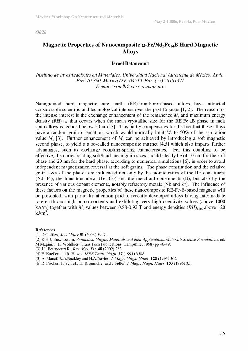
High resolution images are present in figure 3. We can observe single crystal nanowires with length around of 10 µm and an average diameter of 15 to 20 nm. However, some of the wires present multiple twining planes showing a polycrystalline structure. The EDS obtained in nanobeam mode (0.5 nm spot size) shows that the chemical composition of the NW is fundamentally Pb. The wires are growing principally in [111] direction (0.29 nm).
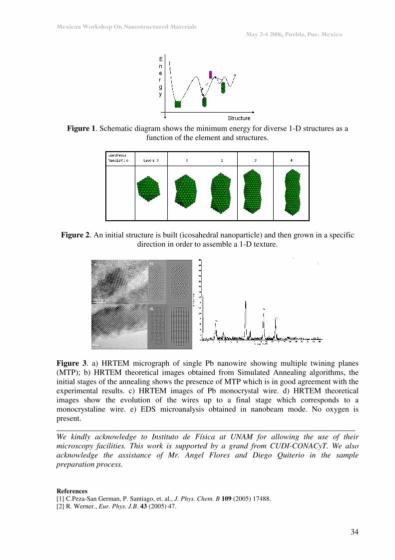
Once we obtained the experimental result we used Montecarlo or Simulated Annealing algorithms to simulate one-dimension Pb nanostructures [2]. This method is based on an aleatory search of minimum structures. The approach to resolve the problem was to find the most stable configuration. Graphical view is shown in figure 1. We built an initial structure and then grew it in a specific direction for Pb element (figure2). We studied the nanowires evolution using Simulated Annealing based in a thermodynamic process. The temperature parameter (T) simulates the potential energy of the structure and system evolution goes to a minimum energy system (Tf). The theoretical models show in figure 3 simulates the evolution of the nanowires during the thermal process. There is a perfect match between the experimental and theoretical results.
���������� ��������� ������������������ �� ��������������������������������������������������������������������������������������������������������������������������������������������������������
34
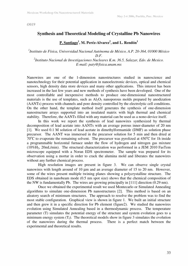
Figure 1. Schematic diagram shows the minimum energy for diverse 1-D structures as a
function of the element and structures.
Figure 2. An initial structure is built (icosahedral nanoparticle) and then grown in a specific direction in order to assemble a 1-D texture.
Figure 3. a) HRTEM micrograph of single Pb nanowire showing multiple twining planes (MTP); b) HRTEM theoretical images obtained from Simulated Annealing algorithms, the initial stages of the annealing shows the presence of MTP which is in good agreement with the experimental results. c) HRTEM images of Pb monocrystal wire. d) HRTEM theoretical images show the evolution of the wires up to a final stage which corresponds to a monocrystaline wire. e) EDS microanalysis obtained in nanobeam mode. No oxygen is present. ___________________________________________________________________________ We kindly acknowledge to Instituto de Física at UNAM for allowing the use of their microscopy facilities. This work is supported by a grand from CUDI-CONACyT. We also acknowledge the assistance of Mr. Angel Flores and Diego Quiterio in the sample preparation process. References [1] C.Peza-San German, P. Santiago, et. al., J. Phys. Chem. B 109 (2005) 17488. [2] R. Werner., Eur. Phys. J.B. 43 (2005) 47.
���������� ��������� ������������������ �� ��������������������������������������������������������������������������������������������������������������������������������������������������������
35
O020
Magnetic Properties of Nanocomposite αααα-Fe/Nd2Fe14B Hard Magnetic Alloys
Israel Betancourt
Instituto de Investigaciones en Materiales, Universidad Nacional Autónoma de México. Apdo.
Pos. 70-360, Mexico D.F. 04510. Fax. (55) 56161371 E-mail: [email protected].
Nanograined hard magnetic rare earth (RE)-iron-boron-based alloys have attracted considerable scientific and technological interest over the past 15 years [1, 2]. The reason for the intense interest is the exchange enhancement of the remanence Mr and maximum energy density (BH)max that occurs when the mean crystallite size for the RE2Fe14B phase in melt spun alloys is reduced below 50 nm [3]. This partly compensates for the fact that these alloys have a random grain orientation, which would normally limit Mr to 50% of the saturation value Ms [3]. Further enhancement of Mr can be achieved by introducing a soft magnetic second phase, to yield a a so-called nanocomposite magnet [4,5] which also imparts further advantages, such as exchange coupling-spring characteristics. For this coupling to be effective, the corresponding soft/hard mean grain sizes should ideally be of 10 nm for the soft phase and 20 nm for the hard phase, according to numerical simulations [6], in order to avoid independent magnetization reversal at the soft grains. The phase constitution and the relative grain sizes of the phases are influenced not only by the atomic ratios of the RE constituent (Nd, Pr), the transition metal (Fe, Co) and the metalloid constituents (B), but also by the presence of various dopant elements, notably refractory metals (Nb and Zr). The influence of these factors on the magnetic properties of these nanocomposite RE-Fe-B-based magnets will be presented, with particular attention paid to recently developed alloys having intermediate rare earth and high boron contents and exhibiting very high coercivity values (above 1000 kA/m) together with Mr values between 0.88-0.92 T and energy densities (BH)max above 120 kJ/m3. References [1] D.C. Jiles, Acta Mater 51 (2003) 5907. [2] K.H.J. Buschow, in: Permanent Magnet Materials and their Applications, Materials Science Foundations, ed. M.Magini, F.H. Wohlbier (Trans Tech Publications, Hampshire, 1998) pp 46-49. [3] J.I. Betancourt R., Rev. Mex. Fis. 48 (2002) 283. [4] E. Kneller and R. Hawig, IEEE Trans. Magn. 27 (1991) 3588. [5] A. Manaf, R.A.Buckley and H.A.Davies, J. Magn. Magn. Mater. 128 (1993) 302. [6] R. Fischer, T. Schrefl, H. Kronmuller and J.Fidler, J. Magn. Magn. Mater. 153 (1996) 35.
���������� ��������� ������������������ �� ��������������������������������������������������������������������������������������������������������������������������������������������������������
36
O021
Metal-dendrimer Nanospecies
Redón, R.1, Mendoza-Martínez, F.1, Morales-Morales, D2. Vázquez-Olmos A. 1, J. M. Saniger1
1Universidad Nacional Autónoma de México, Centro de Ciencias Aplicadas y Desarrollo
Tecnológico, México. 2Universidad Nacional Autónoma de México, Instituto de Química, México. Fax: 5255-
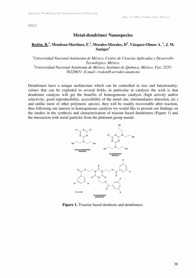
56228651. E-mail: [email protected] Dendrimers have a unique architecture which can be controlled in size and functionality; virtues that can be exploded in several fields, in particular in catalysis the wish is that dendrimer catalysts will get the benefits of homogeneous catalysis (high activity and/or selectivity, good reproducibility, accessibility of the metal site, intermediaries detection, etc.) and unlike most of other polymeric species, they will be readily recoverable after reaction, thus following our interest in homogeneous catalysts we would like to present our findings on the studies in the synthesis and characterization of triazine based dendrimers (Figure 1) and the interaction with metal particles from the platinum group metals.
N
N
N
O
O O
OO
O
O
O
O
R R
R
R
R
R
N N
N Cl
NOHHO
Cl
N N
N NOH
OH
NOHHO
Cl
R = H, OH
mono-substitutedDendron
di-substituteddendron
tri-substitutedDendrimer
Figure 1. Triazine based dendrons and dendrimers.
���������� ��������� ������������������ �� ��������������������������������������������������������������������������������������������������������������������������������������������������������
37
O022 Micro-Raman Investigation of Transition Metal Doped ZnO Nanoparticles
Roberto Sato-Berrú1, América Vázquez-Olmos1, Ana L. Fernández-Osorio2
and Oscar Chávez-Osornio1
1Centro de Ciencias Aplicadas y Desarrollo Tecnológico, 2Facultad de Estudios Superiores Cuautitlán, Universidad Nacional Autónoma de México, C.U., México D.F., 04510, México.
Tel.: 56228602, ext.: 1152, Fax: 56228651. E-mail: [email protected]
There are different methods for introducing new magnetic, optical, electronic and photophysical properties to semiconductor nanocrystals, which are attracting interest as prospects for technological applications in the areas of spintronic and optoelectronic [1]. An effective method for tuning the physical properties of semiconductors materials involves impurity doping. In this sense, Zinc oxide (ZnO) is a leading candidate for such devices due to is a wide-band gap (3.25 eV) semiconductor.
Here, we report the results of the Raman scattering study of ZnO nanoparticles with an average size of 20 nm as well as ZnO doped with 5% of Mn(II), Fe(II) or Co(II). ZnO nanoparticles present a typical Raman peak at 436 cm-1 [2] whereas ZnxMn1-xO, ZnxFe1-xO and ZnxCo1-xO have characteristic peaks at 663, 644 and 678 cm-1 respectively, which have similarity with Mn3O4, Fe3O4 and Co3O4 Raman spectra. Moreover, these samples were analyzed to different laser light intensities. We observed new vibrational modes at 517, 565 and 527 cm-1 seems specific for the Mn, Fe and Co dopants, respectively, ZnO did not reveal additional modes. References [1] Németh, J.; Rodríguez-Gattorno, G.; Vázquez-Olmos, A. R.; Díaz, D.; Dékány, I. Langmuir 20 (2004) 2855. [2] Bundesmann C.; Ashkenov N.; Schubert M.; Spemann D.; Butz T.; Kaidashev E.M.; Lorenz M. and Grundmann M. Appl. Phys. Lett. 83 (2003) 1974.
���������� ��������� ������������������ �� ��������������������������������������������������������������������������������������������������������������������������������������������������������
38
O023
Ballistic Effect and Photoluminescence of Si Nanocrystallite Structures
T. V. Torchynska and F. Becerril Espinoza
ESFM-Instituto Polit�cnico Nacional, Ed. 9, U.PA.L.M., M�xico 07738, M�xico. E-mail: [email protected]
Nanoscaled Si structures continue to be of interest for their potential application as stable silicon based light emitting materials, photo sensors and memory devices. Two groups of Si NC systems have been discussed. The first class of systems deals with Si NCs of the small sizes (a � aB, where aB is the exciton Bohr radius equal for Si NCs to 4.8 nm). This case is known as strong quantum confinement regime. The optical properties in such NC systems are controlled by the quantum confinement effect. The second class of systems deals with NCs of the big sizes of 10-200 nm. For this case the quantum confinement models in emission and electronic transport do not work.
It is shown that PL spectra of the second class of Si NC systems, such as magnetron co-spattered Si NCs-SiOx or Si NCs in amorphous Si, as well as specially prepared porous-Si, consist of the visible PL bands mainly peaked at 1.70-1.80 and 1.90-2.10 eV. The dependence of 1.70-1.80 and 1.90-2.10 eV PL and PL excitation spectra on Si NC sizes in the range of 10-200 nm has been investigated. The experimental PL results were analyzed from the point of view of new concept based on the hot carrier ballistic effect in the PL excitation of interface related defects. Numerical calculation of this PL model has been done. The dependence of the 1.70 eV PL band intensity on Si NC sizes was numerically calculated and the well correlation of calculated and experimental results has been obtained. To verify of hot carrier ballistic transport role in PL excitation of Si NCs the effect of magnetic field on the 1.70 eV PL band has been studied. On the base of this investigation the effective mobility of hot electrons is estimated as 6000 cm2/Vs, which greatly exceeds normal electron mobility (1900 cm2/Vs) in Si and thus confirms the presence of hot carrier ballistic motion. ___________________________________________________________________________ This work was supported by CONACYT (Project U42436-Y) and CGPI-IPN Mexico.
���������� ��������� ������������������ �� ��������������������������������������������������������������������������������������������������������������������������������������������������������
39
P001
Self-Assemble of AuxAg1-x Alloy Nanoclusters in Silanised Glass Plates
J. A. Pescador-Rojas1, L. Nolasco-Hernández2, M. E. Sánchez-Espindola3, A. Bautista-Hernández4, J. L. Herrera-Pérez1 and J. F. Sánchez-Ramírez1
1 CICATA-IPN, Legaría 694, Col. Irrigación, 11500 México D.F., México.
E-mail: [email protected] 2 Instituto de Física, Universidad Autónoma de Puebla, Apdo. Postal J-48, Puebla, Puebla.,
72570, México 3 Central de Instrumentación de Microscopia, ENCB, IPN
4 Facultad de Ingeniería, Universidad Autónoma de Puebla, Puebla, Puebla., 72570, México. We described the self-assemble process of colloidal dispersions of polymer-protected AuxAg1-
x alloy nanoparticles. AuxAg1-x (0.1 � x � 0.9) colloidal nanoclusters were prepared by simultaneous reduction of their metal precursors at temperature by sodium borohydride in the presence of the protective polymer poly(N-vinyl-2-pirrolidone) (PVP) and attached to aminopropyltrimethoxysilane treated glass plates. The polymer not only serves as the protective layer for the nanoparticles but also provides ketone functional groups to stop chemo selective bond reactions. The assemblies of AuxAg1-x alloy nanoparticles of various compositions were characterized by UV-Vis spectroscopy, atomic force microscopy (AFM) and transmission electron microscopy (TEM). Mechanism and optimum incorporation conditions are studied by UV-Vis and IR spectroscopy, atomic force microscopy (AFM), and transmission electron microscopy (TEM). ___________________________________________________________________________ The authors are thankful to the Mexican Agencies, CONACyT, CGPI-IPN for financial supports.
���������� ��������� ������������������ �� ��������������������������������������������������������������������������������������������������������������������������������������������������������
40
P002 Atomic Simulation of Fracture of Nano-Single Crystal of Nickel in Tension
A. Bautista-Hernández1, M. Salazar-Villanueva2, J. F. Sánchez-Ramírez3
and A. Macias-Cervantes1
1Facultad de Ingeniería, Benemérita Universidad Autónoma de Puebla, Apdo. Postal J39, Puebla, Pue., 72570, México
2Instituto de Física, Benemérita Universidad Autónoma de Puebla, Apdo. Postal J-48, Puebla, Pue., 72570, México.
3CICATA-IPN, Legaria 694 Col. Irrigación, México D.F. The effect of the hydrostatic and uniaxial stress in a nano-single face-centered cubic lattice has been studied. Molecular dynamics simulations using Sutton-Chen potential for nickel has performed at several temperatures and deformations. In this work, the value of the maximum stress of fracture as function of applied deformation is discussed. ___________________________________________________________________________ This work has been supported by VIEP (BUAP) and CGPI (IPN).
���������� ��������� ������������������ �� ��������������������������������������������������������������������������������������������������������������������������������������������������������
41
P003
Microestructura de Superficies Irradiadas
Carlos Camacho Olguín y Arturo García Bohórquez Departamento de Ciencias de los Materiales de la Escuela Superior de Física y Matemáticas.
Instituto Politécnico Nacional. U.P. “Adolfo López Mateos”, C.P.07738, México, D.F. E-mail: [email protected]
El bombardeo de superficies con iones de energía moderada puede generar el desarrollo de varios tipos de estructuras de tamaño micrométrico e inclusive nanométrico. Estas estructuras incluyen ranuras, escalones, terrazas lisas, poros, conos, etc. Los fenómenos responsables de la producción de estas microestructuras son la erosión, reflexión del ion, redeposición del material erosionado y la difusión superficial de átomos de impurezas o de la matriz.
Con el fin de estudiar el daño superficial ocasionado en el material por la irradiación, se bombardeo la aleación Ni22%at.Si, en un acelerador lineal tipo Tandetron GIC (Berger-1986) con iones Ni de 3.66 MeV a 650°C y 1000 nA/h. La aleación Ni22%at.Si, solidifica eutecticamente. Se caracterizó el eutectico, usando difracción de rayos X y análisis métalográfico, se encontró que el intermetálico Ni3Si esta presente en dos formas cristalinas cúbica y monoclínica, se encuentra disperso en una matriz de la solución sólida. Su morfología es laminar, las dimensiones de las fases son del orden de micrones.
Para caracterizar la morfología de la superficie irradiada de la aleación, hemos empleado los microscopios óptico, electrónico de barrido y de fuerza atómica. Las imágenes obtenidas en estos microscopios, nos han permitido identificar y medir, las características de la morfología de la superficie, que consiste de un arreglo regular de ondulaciones, con un periodo promedio de 2.3 µm y una altura promedio de 33 nm. Concluimos que estas ondulaciones o canales han sido producto de una erosión preferencial inducida por la irradiación, de una de las dos fases del eutectico.
���������� ��������� ������������������ �� ��������������������������������������������������������������������������������������������������������������������������������������������������������
42
P004
Mechanical Analysis-Geometric of Ti Nanoparticles: An FEA about Mechanical Efficiency
E. Gómez Hernandez1,2
1Instituto Tecnológico Superior de la Sierra Norte de Puebla, Av. José L. Martínez Vázquez
No. 2000, Zacatlán, Puebla; C. P. 73310. México 2Universidad Popular Autónoma del Estado de Puebla, 21 sur 1103, Col. Santiago, Puebla,
Pue., México. E-Mail: [email protected] The creation of different materials through the nanotechnology has provided a field of investigation and development that promises to offer new solutions to the necessities of this field of study. Nevertheless, the systems created until now cannot stop in the limited implementation of Nanoparticles metallic (or added metallic) shrunk in diverse substrates, with the purpose of improving the own characteristics of the materials, now is necessary to satisfy a greater necessity: to optimize the materials that have been created by means of the correct selection of their geometry. The analysis presented/displayed in this work proposes a method that reveals the narrow relation that exist between the geometric optimization of particles and the possible applications in a study field in which not yet the sufficient thing has been included.
���������� ��������� ������������������ �� ��������������������������������������������������������������������������������������������������������������������������������������������������������
43
P005
A Topological Approximation on the Understanding of Small Clusters
E. L. Juárez1,2, J. A. Lombardero2, 3, J. A. Ascencio4
1Facultad de Ciencias de la Electrónica, Benemérita Universidad Autónoma de Puebla, Ave.
San Claudio y 18 sur, s/n CU, San Manuel, Puebla, Pue. 72570, México 2Universidad Popular Autónoma del Estado de Puebla, 21 sur 1103, Col. Santiago, Puebla,
Pue. CP72000 México 3Universidad La Salle Benavente, 25 Oriente. 9, Col. El Carmen, Puebla, Pue. CP72000
México 4Instituto Mexicano del Petróleo, Eje Central Lázaro Cárdenas 152, Col. Sn Bartolo
Atepehuacan, México, D.F., CP07730, México. E-mail:. [email protected] Topological and geometrical effects are among the most striking quantum phenomena discovered since the creation of quantum mechanics in 1926. Basic assumptions about the role of potentials in physics and its discovery prefigured a revolution in our understanding of the fundamentals forces of nature. In the other hand, the small particles do not follow the bulk arrays, they search for the lower surface energy configurations [1], their own shape correspond also to morphologies that must be related to the capacity of a method to reduce the superficial energy and to reduce the atoms to the metal oxidation state. Many molecular dynamics have been applied to establish the tendencies to produce one or other structure [2]. However, it is well known that no all the particles will reach the minimum energy configuration. We study the use of topological methods to determine the tendency of a nanoparticle to adopt a particular shape and the understanding of the contribution of faces, vertices and superficial array. This work will show a brief report of the first steps to associate both disciplines for pure mathematics and quantum mechanics. References [1] M. José Yacamán, J. A. Ascencio and H. B. Liu, J. Gardea-Torresdey. J. Vac. Sci. Technol. B 19 (2001) 1091. [2] H. B. Liu, J. A. Ascencio, M. Perez-Alvarez, and M. J. Yacaman. Surface Science 491 (2001) 88.
���������� ��������� ������������������ �� ��������������������������������������������������������������������������������������������������������������������������������������������������������
44
P006
Molecular Dynamics of Icosahedral Au-Pd Alloy Clusters
Sergio J. Mejía-Rosales, Alejandra J. Gutiérrez-Esparza, Carlos Fernández-Navarro, Eduardo Pérez-Tijerina
Facultad de Ciencias Físico-Matemáticas, Universidad Autónoma de Nuevo León, San
Nicolás de los Garza, Nuevo León, México 66450 E-mail: [email protected], [email protected]
Juan M. Montejano-Carrizales
Instituto de Física, Universidad Autónoma de San Luis Potosí, San Luis Potosí, S.L.P.,
México 78000
Miguel José-Yacamán Chemical Engineering Department and Texas Advanced Materials Center, The University of
Texas at Austin, Austin Texas 78712, USA. Phone: 8183294030, Fax: 8183522954. Using a Sutton and Chen inter-atomic potential, we study the molecular dynamics of Au-Pd alloy clusters with an icosahedral structure at different temperatures and concentrations, where each concentration of the 561-atoms clusters was made by setting the atoms at certain equivalent sites, in order to identify under which conditions the melting transition temperature appears for each cluster. In addition, we compute the diffusion coefficient and order parameters for each atomic species in order to correlate the obtained results with the caloric curves of each cluster. As a result, we observe that the melting transition temperature depends on the relative atomic positions of gold and palladium. Also, we find that the melting transition temperature of the Au-Pd alloy clusters appears at higher temperature than that of the pure-gold cluster. From the analysis of the structural succession of the clusters, we found that the melting temperature of gold increases because of the presence of palladium, and for those clusters with a higher concentration of palladium on the surface, we observe an early migration of gold atoms before the melting transition temperature appears.
���������� ��������� ������������������ �� ��������������������������������������������������������������������������������������������������������������������������������������������������������
45
P007
Obtención de la Difusividad Térmica en Líquidos Conteniendo Nanopartículas de Oro Usando la Técnica de Lente Térmica
R. Gutiérrez Fuentes, J.L. Jiménez Pérez, J.F. Sánchez Ramírez, R. Carbajal Valdez
Cicata-IPN, Legaria 694, Col. Irrigación, 11500, México D.F. E-mail: [email protected]
A. Cruz Orea
Depto. Física, Cinvestav – IPN, A.P. 14-740, 07300, México D.F.
Fluidos conteniendo nanopartículas de oro (Au) con diferentes tamaños (12-40 nm) fueron preparados en una solución de agua. Usando el montaje experimental de la técnica de Lente Térmica, la difusividad térmica de las suspensiones fue obtenida. En esta técnica se uso el modo aberrante de lente térmica con laseres arreglados en el modo desacoplado. La constante del tiempo característico del transiente de la técnica de lente térmica fue obtenida por el ajuste de la expresión teórica, para el transiente de lente térmica, a los datos experimentales. Del tiempo característico de la formación de la lente térmica, fue obtenida la difusividad térmica del fluido. La espectroscopia UV-Vis y TEM fueron usados para caracterizar las suspensiones. Los resultados de la Lente Térmica muestran que la difusividad térmica de la suspensión aumenta con el incremento del tamaño de la nanopartícula.
���������� ��������� ������������������ �� ��������������������������������������������������������������������������������������������������������������������������������������������������������
46
P008 CVD Growth of Carbon Nanotubes from Alcohol on Porous Alumina Using
Fe, Co and Mo Catalysts
G. Ortega-Cervantez, J. Ortiz-López, G. Rueda-Morales y C. Mejía-García
Escuela Superior de Física y Matemáticas, I.P.N. Edificio 9, UPALM, 07738 México, D.F. Fax. 5586-2957, 5586-2825, 5729-6000 ext. 55051. E-mail: [email protected]
Carbon nanotubes are synthesized by CVD (chemical vapor deposition) using ethanol as carbon source. Catalysts are Fe, Mo y Co obtained from their corresponding acetates dissolved in ethanol. Acetate solutions are deposited on porous alumina substrates by dripping or by dip coating. Nanotubes grow with 30 to 100 nm diameter after 20 min exposure to ethanol vapor and temperatures of 650, 700, 830 y 850°C. Sample analysis is performed with scanning electron microscopy and Raman spectroscopy.
���������� ��������� ������������������ �� ��������������������������������������������������������������������������������������������������������������������������������������������������������
47
P009 Structural Selection and Amorphization of Small Ni-Ti Bimetallic Clusters
H. B. Liu,1 G. Canizal,2 P. S. Schabes-Retchkiman3 and J.A. Ascencio1
1Programa de Investigación en Ductos, Corrosion y Materiales, Instituto Mexicano del Petroleo, Eje Central Lázaro Cárdenas 152, Col. San Bartolo Atepehuacan, C.P.07730,
Mexico D.F., Mexico. E-mail: [email protected] 2CECyD (Unidad Allende), Instituto Politécnico Nacional, Allende No. 38, Centro, México
D.F. 06010, México. 3Instituto de Física, Universidad Nacional Autonoma de Mexico, Apartado Postal 20-364,
Mexico, Distrito Federal, C.P.01000, México. Classical molecular dynamics simulation is used for structural thermodynamic analysis of Ni-Ti bimetallic clusters. Experimental observation for the nanoclusters synthesized by bio-reduction method is used to consolidate the conclusion. The results demonstrate that the Ni-Ti nanoclusters as small as 2-3 nanometers are not energetically favorable for the common ordered geometrical arrangements as such cuboctahedron, decahedron and icosahedron, though they can be synthesized experimentally. For the elemental distribution, the Ni and Ti tend to aggregate separately. In the cases under study, eutectic-like and Ni-core/Ti-shell structures can keep their basic shape and elemental distribution during long period of relaxation at room temperature. For the other cases as such solid solution, Ti-core/Ni-shell, the structures amorphized and the elementals tend to distribute uniformly even though they are in a temperature as low as room temperature. Experimental evidences were obtained by the analysis of biosynthesized nanoparticles using transmission electron microscopy techniques. This allowed determining the partial amorphized structures of small bimetallic particles with cubic and multiple twined like structures.
���������� ��������� ������������������ �� ��������������������������������������������������������������������������������������������������������������������������������������������������������
48
P010
Synthesis of Stable Bimetallic Ru-Pt Nanoparticles
I. Moreno-Preza1, C. Luna Pérez1, P. Santiago2, and U. Pal3
1) Facultad de Ingeniería Química, Universidad Autónoma de Puebla, 18 Sur y Av. San
Claudio, C.U., Puebla 72570, Mexico. 2) Instituto de Física, Universidad Nacional Autónoma de Mexico, A.P. 20-365, C.P. 01000,
México D.F., Mexico. 3) Instituto de Física, Universidad Autónoma de Puebla, Apdo. Postal J-48, Puebla, Pue.
72570, Mexico. E-mail: [email protected] Synthesis of bimetallic nanoparticles of stable and non-dispersive size with controlled geometries is of immense importance for their technological applications. Optimizing the synthesis parameters, we prepared stable and size controlled Ru-Pt bimetallic nanoparticles of different compositions through simultaneous chemical reduction of their chloride salts. The nanoparticles are extremely stable, with no size variation over a period of several months at room temperature. It is seen that the contents of both the reductor and passivating agent play roles on the stability of the nanoparticles. While the insufficient reductor content permits a post nucleation growth of the nanoparticles leading their size increase with time, an insufficient content of passivating agent favors their thermal agglomeration at room temperature. By controlling the contents of reductor and passivating agent, we could synthesize stable bimetallic Ru-Pt nanoparticles of different compositions. The stability of the nanoparticles was monitored by UV-Vis optical absorption spectroscopy. The size, size distribution and structure of the nanoparticles were studied through transmission electron microscopy. ___________________________________________________________________________ The work is supported partially through VIEP-BUAP-CONACyT, Mexico (Grant No. 11/I/EXC/05)
���������� ��������� ������������������ �� ��������������������������������������������������������������������������������������������������������������������������������������������������������
49
P011
Fe Nanoparticles Produced by High Energy Ball Milling Processes
J. E. Muñoz G., J. Cervantes, R. Esparza and G. Rosas
Instituto de Investigaciones Metalúrgicas, UMSNH, Edificio U, Ciudad Universitaria, Morelia, Mich. 58000, MEXICO. E-mail: [email protected]
In this investigation, the chemical and microstructural characteristics of Fe nanoparticles synthesized by high energy ball milling have been explored. Interest in magnetic nanoparticles remains high because of the wide range of potential applications. The structure, morphology and compositions of the powders were obtained using X-ray diffraction patterns and high resolution electron microscopy. HREM images confirmed the nanoparticles presence with approximately 2-4 nm in size. It was found that this nanoparticles size range is smaller in comparison with other synthesis methods. Also, it was confirmed by HREM images that the obtained nanoparticles were mainly of the FCC nature and some of them of the MTP type. Hence, high energy ball milling demonstrated to be a suitable technique to develop Fe nanoparticles.
���������� ��������� ������������������ �� ��������������������������������������������������������������������������������������������������������������������������������������������������������
50
P012 A New Type of Pd Catalyst from A Dendron-PCP Pincer for Heck Coupling
Reactions
Redón R.1, Mendoza Martínez F.1, Morales-Morales, D.2
1Centro de Ciencias Aplicadas y Desarrollo Tecnológico, México, DF 04510, Mexico
Phone: (+52-55) 56228602, ext. 1154; Fax: +52-55-56228651 2Instituto de Quimica, Universidad Nacional Autonoma de Mexico, Coyoacan, C.P. 04510,
Mexico. Phone: (+52-55) 56 22 45 14, Fax: (+52-55) 56 16 22 17 E-mail: [email protected], [email protected]
Nowadays the development of well-defined Pd catalyst for Heck coupling reactions is investigated to give not only high activities and yields in homogenous systems but in green chemistry with cheaper and handling reagents. This environment encouraged us to obtain a new type of homogenous catalyst that could be easy prepared and recover.
Polymeric nanostructures like dendrimers seem to be good ligands for controlling metal nanoparticles size and dispersion. These could be made by including a PCP pincer ligand in a dendrimer. Because the big size of this type of functional-hyperbranched structures seems to be potentially recover by anodic porous alumina membranes, avoiding annoying procedures and reducing costs. Thus, we would like to present our latest results on the synthesis and characterization of dendrimer as well as conditions for preparing PCP ligand before the preparation of the nanocomposites with palladium nanoparticles. A later work will be proven this material as homogenous catalyst in Heck coupling reactions.
���������� ��������� ������������������ �� ��������������������������������������������������������������������������������������������������������������������������������������������������������
51
P013
Microstructural Study of Nanocrystalline Mg-Zn Alloys Produced by Mechanical Alloying
A. F. Palacios-Lazcano, J. L. Luna-Sánchez, L. F. Dámaso-Custodio
and J. G. Cabañas-Moreno1
Instituto Politécnico Nacional, ESFM, Depto. de Ciencia de Materiales, Unidad Prof.
“ALM”, Col. Lindavista, Apdo. Postal 75-373, México D.F., 07300. México E-mail: [email protected], [email protected]
Mg-Zn alloys of various compositions have been obtained by mechanical alloying in a planetary type ball mill of Mg–Zn elemental powders mixtures. Mg-Zn alloys were obtained with the purpose of forming a nanostructured material which store hydrogen in the solid state and to improve the kinetics in the hydriding-dehydriding process.
The powders mixtures were milled during 216 ks under argon atmosphere. The mechanical alloyed powders have been characterized by Scanning Electron Microscopy (SEM), Energy Dispersive X-Ray Spectrometry (EDS), X-Ray Diffraction (XRD) and Transmission Electron Microscopy (TEM) techniques.
Mg-Zn alloyed powders consist of agglomerated particles with a size between 10 and 20 µm. EDS results does not report changes with the nominal composition. Quantitative phase analysis, crystallite size and microdeformation have been determined by Rietveld analysis of the XRD data.
���������� ��������� ������������������ �� ��������������������������������������������������������������������������������������������������������������������������������������������������������
52
P014
Synthesis, Characterization and Simulation of Ag Tetrahedral Nanoparticles
Miguel Ángel Gracia Pinilla, Joel Antúnez Garcia, Alfredo Tlahuice Flores, Sergio J.
Mejía-Rosales, Carlos Fernández-Navarro, Eduardo Pérez-Tijerina
Laboratorio de Nanociencias y Nanotecnología, Facultad de Ciencias Físico-Matemáticas, Universidad Autónoma de Nuevo León, San Nicolás de los Garza, Nuevo León, México
66450. Phone: 8183294030, Fax: 8183522954. E-mail: [email protected]
Miguel José-Yacamán
Chemical Engineering Department and Texas Advanced Materials Center, University of Texas at Austin, Austin Texas 78712, USA
In the present work we study the synthesis of Ag nanoparticles, their structural, morphological and chemical characterization, as well as their optical properties, by the use of the techniques of X-ray diffraction (XRD), scanning electron microscopy (SEM), transmission electron microscopy of (TEM), atomic force microscopy (AFM), scanning auger microscopy (SAM), and UV-visible spectroscopy. The Ag nanoparticles were produced by magnetron sputtering, followed by thermalization and condensation in high pressure zones. The size of the nanoparticles is controlled through the handling of three variables: flow of gases (Ar and He), power (Watts), and aggregation zone length.
The shape of the obtained Ag nanoparticles is tetrahedral, with 5 nm in height (measured with AFM), that corresponds approximately to a 2925-atom perfect tetrahedron. We used both DFT and MD to simulate the structures, obtaining that the tetrahedra are as stable as the cuboctahedra of roughly the same size, and that their melting point is close to that of the bulk. The spectrum of absorption shows a shift related the effect of the shape of the nanoparticles. ___________________________________________________________________________ Acknowledgment: This work was supported by the Council for Science and Technology of the State of Nuevo León.
���������� ��������� ������������������ �� ��������������������������������������������������������������������������������������������������������������������������������������������������������
53
P015
Lattice Measurements of Icosahedral Au-Pd Nanoparticles
Daniel Santiago-González, Sergio J. Mejía-Rosales, Eduardo Pérez-Tijerina
Laboratorio de Nanociencias y Nanotecnología, Facultad de Ciencias Físico-Matemáticas, Universidad Autónoma de Nuevo León, San Nicolás de los Garza, Nuevo León, México 66450
Juan M. Montejano-Carrizales
Instituto de Física, Universidad Autónoma de San Luis Potosí, San Luis Potosí, S.L.P., México 78000
Miguel José-Yacamán
Chemical Engineering Department and Texas Advanced Materials Center, The University of
Texas at Austin, Austin Texas 78712, USA The structure of several metallic nanoparticles is analyzed through Molecular Dynamics simulations, to investigate how the interplanar distance d (111) is affected by the relative concentrations of the atomic species in the particle, and the existence of vacancies in the outer atomic shells of the particle. In particular we study bimetallic Au-Pd icosahedral nanoparticles, calculating the d (111) for different concentrations of Au and Pd atoms. The results obtained are shown in a chart. The calculations were made with a program we have developed. We found that the value of d (111) depends strongly on the local concentration of the atomic species. We compare our results with measurements made by electronic microscopy, finding a fair agreement between them.
���������� ��������� ������������������ �� ��������������������������������������������������������������������������������������������������������������������������������������������������������
54
P016
Synthesis and Structural Characterization of Sulfur Nanowires
P. Santiago1, E. Carvajal2, D. Mendoza3, and L. Rendón1
1Instituto de Física, Universidad Nacional Autonoma de México, A.P. 20-364, 01000 México
2Facultad de Ciencias, U.N.A.M., A. P. 70-646, 04510 México, D.F. 3Instituto de Investigaciones en Materiales, U.N.A.M., A.P. 70-360, 04510 México, D.F.
Sulfur is one of the most studied elements due to its technological applications. For example, as molecular electronic devices, sulfur has the susceptibility to bond with gold and other metal surfaces [1]. It is also well known that sulfur plays an important role in the chemistry of interstellar medium and used to form stable carbon chains such as C3S and C5S, actually carbon nanotubes have been functionalized with these C-S chains in order to obtain hybrid materials with useful properties for gas sensor and catalytic applications [2].
In the present work we report the synthesis of single crystalline Sulfur nanowires at room temperature using anodic alumina nanoporous templates (AANTs) with an average porous inner-diameter of 20 nm [3]. We used S-CS2 (10g in 40 ml) as solution phase precursor. The AANT was immersed in the precursor solution for 5 days in a special flask to fill the alumina porous. The AANT´s were dried at room temperature in order to evaporate the CS2 remaining solvent in a safe extractor system. The structural characterization was performed in a JEM 2010 FasTem microscope equipped with a Noran EDS spectrometer. The sample was prepared for its observation using a mortar in order to crack the alumina mold and liberates the nanowires without any further chemical process.
From the TEM studies we found both curly and straight nanowires. The sulfur nanowires diameter is between 15 to 20 nm and about 1000 nm length. Figure 1b corresponds to a HRTEM micrograph where is possible to observe the lattice space parameter which corresponds to d= 0.295 nm. This lattice parameter is in good agreement with the reflection (140) for the Monoclinic S8 phase (PCPDF file 86-1278), however the structural characterization is still under study. There are also bending wires (figure 2a) where it is possible to observe stacking faults defects. A chemical elemental microanalysis was also performed in nanobeam mode (figure 2b); the carbon peak observed corresponds to the grid support. In some monocristalline wire zones we could observe that the preferential grown axis corresponds to [140] for the monoclinic Sulphur structure, however we are studying the phase under mathematical simulated methods in order to understand the structure.
Differential scanning calorimetry measurements were also performed for this system. However, the preliminary results are not in agreement with the bulk sulfur data reported in the literature. We found that the characteristic temperatures associated with the bulk sulfur transformations are different to the corresponding with our 1-D sulfur structures.
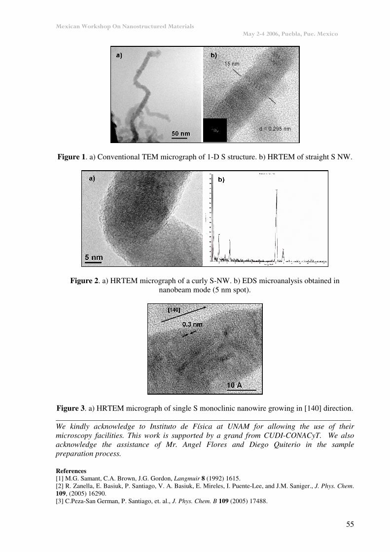
���������� ��������� ������������������ �� ��������������������������������������������������������������������������������������������������������������������������������������������������������
55
Figure 1. a) Conventional TEM micrograph of 1-D S structure. b) HRTEM of straight S NW.
Figure 2. a) HRTEM micrograph of a curly S-NW. b) EDS microanalysis obtained in nanobeam mode (5 nm spot).
Figure 3. a) HRTEM micrograph of single S monoclinic nanowire growing in [140] direction. ___________________________________________________________________________ We kindly acknowledge to Instituto de Física at UNAM for allowing the use of their microscopy facilities. This work is supported by a grand from CUDI-CONACyT. We also acknowledge the assistance of Mr. Angel Flores and Diego Quiterio in the sample preparation process. References [1] M.G. Samant, C.A. Brown, J.G. Gordon, Langmuir 8 (1992) 1615. [2] R. Zanella, E. Basiuk, P. Santiago, V. A. Basiuk, E. Mireles, I. Puente-Lee, and J.M. Saniger., J. Phys. Chem. 109, (2005) 16290. [3] C.Peza-San German, P. Santiago, et. al., J. Phys. Chem. B 109 (2005) 17488.
���������� ��������� ������������������ �� ��������������������������������������������������������������������������������������������������������������������������������������������������������
56
P017
Structural Characteristics of Chemically Synthesized Au Nanoparticles
R. Esparza1, G. Rosas1, M. López-Fuentes2, U. Pal2 and R. Pérez4
1Instituto de Investigaciones Metalúrgicas, UMSNH, Edificio U, Ciudad Universitaria,
Morelia, Mich. 58000, MEXICO. E-mail: [email protected] 2Instituto de Física, Universidad Autónoma de Puebla, Apdo. Postal J-48, Puebla, Pue.
72570, MEXICO. 3Instituto Mexicano del Petróleo, Eje Central Lázaro Cárdenas No 152, Col. San Bartolo
Atepehuacan, México D. F., 07730, MEXICO. Metal nanoparticles exhibit unusual chemical and physical properties different from those of the bulk metal, and have a number of fascinating potential applications in heterogeneous catalyst as well as microelectronic and optoelectronic devices. In the present work, a chemical reduction method is used to produce nanometric gold particles. Depending of the concentration of the main reactant compound, nanoparticles of different sizes and consequently different atomic structural configurations are obtained. Insights on the structural nature of the gold nanoparticles are obtained through the comparisons between digitally processed experimental HREM images and theoretically simulated HREM images obtained with the multislice approach of the dynamical theory of electron diffraction. The main structures obtained are fcc-like and decahedral morphologies with fivefold symmetry axes. Using quantum mechanic approximation, the electrostatic potential, the charge density distribution, Fukui field and the corresponding HOMO-LUMO distributions were calculated. These parameters allow a really complete characterization and structure determination. ___________________________________________________________________________ The work is partially supported by VIEP-BUAP-CONACyT, Mexico (Grant # 11/I/EXC/05).
���������� ��������� ������������������ �� ��������������������������������������������������������������������������������������������������������������������������������������������������������
57
P018 Vibration Instabilities and Ideal Stress-Strain in the Cluster Si7 Under Axial
Deformation
M. Salazar-Villanueva1, P. H. Hernández Tejeda1, J. F Rivas Silva1, J. A. Ascencio-Gutiérrez2, and A. Bautista Hernández3
1Instituto de Física, Universidad Autónoma de Puebla, Apdo. Postal J-48, Puebla, Pue.,
72570, México. E-mail: [email protected] 2Programa de Investigación y Desarrollo de Ductos, Instituto Mexicano del Petróleo, Eje
Central Lázaro Cárdenas 152 Col. San Bartolo Atepehuacán, CP 07730, México, D.F., México
3 Facultad de Ingeniería, Universidad Autónoma de Puebla. We present the stress-strain diagram calculation, obtained under axial tension in the yyε direction. Our results are compared with those made by Kitamura et al 1, for Si6 cluster, finding a good agree with them. To test the vibration stability of cluster, we obtained the frequencies as function of the deformation. Found out that the ´´
2e mode vibration makes unstable the Si7 cluster approximately at 0.027 value. The maximum ideal strength is obtained from the vibration frequency calculation but not from the stress-strain diagram, due the fact that the instability appears before maximum stress-strain diagram. All calculations were carried out within the framework of Density Functional Theory using the GGA approximation proposed by Perdew and Wang. References [1] Kitamura Takayuki, Yoshita Ameno and Akihiro Kushima. Materials Science Forum. 482 (2005) 25.
���������� ��������� ������������������ �� ��������������������������������������������������������������������������������������������������������������������������������������������������������
58
P019
Microwave Assisted Synthesis Of NiCr Nanoparticles A. Duhart1, A. García, L. Morán1, R. Noriega 1, R. Cué1, Mario A. Martínez Hernández2
and S.Velumani1
1Department of Physics, ITESM - Campus Monterrey, Monterrey, NL, C.P.64849, Mexico. Email: [email protected], [email protected]
2Centro de Innovación en Diseño y Tecnología, Area de Diseño Mecánica y Automatización, División de Ingeniería y Arquitectura, ITESM - Campus Monterrey, Monterrey, NL,
C.P.64849, Mexico In the past few decades considerable efforts have been devoted to bimetallic nanoparticles owing to their special properties that are brought about by the changes on surface and structure caused by alloying or due to core–shell. Control of composition distribution and particle size of bimetallic nanoparticles is crucial to the improvement of particle properties. In general, bimetallic nanoparticles can be prepared by simultaneous reduction or by successive reduction of two metal ions in the presence of suitable stabilizer. The work presented here deals with the preparation of NiCr nanoparticles via chemical methods from the corresponding chlorides. The synthesis was done using the conventional microwave ovens as a heat source. The heating cycle is optimized to ensure that the reagents are kept at a reasonably constant temperature. The dependence of nanoparticle parameters (such as size and stoichiometric composition) on the heating time is explored. The structural and elemental characterizations of the synthesized NiCr nanoparticles were carried out using XRD and SEM. The synthesized nanoparticles were deposited on the steel and aluminium substrates to explore its corrosion resistance properties for a potential coating on bipolar plates of PEM fuel cells.
���������� ��������� ������������������ �� ��������������������������������������������������������������������������������������������������������������������������������������������������������
59
P020
Comparison of the Experimental Results of Pd-Co-Au Composite with Molecular Simulation
Andrés Vargas Lugo Cantú1, Mauricio Garza Castañón2, Carlos Eduardo Ortiz Dìaz1,
H.B. Liu3, Mario A. Martinez1, and S. Velumani1
1Instituto Tecnològico y de Estudios Superiores de Monterrey – campus Monterrey, E.Garza
Sada #2501, Monterrey, C.P.64849, NL, México. E-mail: [email protected] 2Facultad de Ciencias Físico-Matemáticas, UANL, Monterrey, México.
3Instituto Mexicano del Petróleo, D.F. México. Pt has been the cathode electrocatalyst of choice since the first fuel cell experiments and there has been an intense search for less expensive, more abundant non-platinum electrocatalysts that can offer acceptable performance. Pd-Co-Au (70:20:10 at%) was found to exhibit good catalytic activity for the ORR for Proton Exchange Membrane (PEM) fuel cell and the present work aims to simulate the Pd70Co20Au10 ternary alloy and cross check the already obtained experimental results. XRD analysis for PdCoAu compound has been reported as an FCC structure with well defined peaks in the pattern. An Atomistic model of the structure was developed to obtain similar XRD diffraction pattern and reported. Recent investigations have shown that this alloy has very good and stable electrochemical properties. The main electrochemical properties were simulated using Density Functional Theory and Molecular Dynamics. Since this is an isomeric material each single crystal might have a different atomic distribution hence different characteristic. We propose a crystalline structure for which we obtained similar electrical and catalytic characteristics of that of the experimental results obtained for the Pd-Co-Au composite. Apart from that, by inserting the CO and S atoms in the matrix the poisoning effect of these elements were analyzed and reported.
���������� ��������� ������������������ �� ��������������������������������������������������������������������������������������������������������������������������������������������������������
60
P021
Comparison of the Experimental Results of Pd-Co-Mo Composite With Molecular Simulation
Carlos Eduardo Ortiz Dìaz1, Mauricio Garza Castañón2, Andrès Vargas Lugo Cantú1,
H.B.Liu3, Mario A.Martinez1, S.Velumani1
1Instituto Tecnològico y de Estudios Superiores de Monterrey – campus Monterrey, E.Garza
Sada #2501, Monterrey, C.P.64849, NL, Mexico. E-mail: [email protected] 2Facultad de Ciencias Físico-Matemáticas, UANL, Monterrey, México.
3Instituto Mexicano del Petróleo, D.F. Mexico. Platinum supported on carbon black is widely used as the electrocatalyst for the oxygen reduction reaction (ORR) in proton exchange membrane fuel cells (PEMFC) due to its high catalytic activity and excellent chemical stability in the fuel cell environment. However, platinum is expensive and the limited world’s supply of platinum poses serious problems for a widespread commercialization of the fuel cell technology. These difficulties have created enormous interest in the search for less expensive, more efficient electrocatalysts as well as in lowering the catalyst loading. In order to identify alternative electrocatalysts, non-platinum based metal combinations, inorganic and organometallic complexes, and porphyrins have been investigated over the years for ORR, but they generally exhibit lower catalytic activity than Pt. Recently, there were reports of palladium based electrocatalysts, Pd-Co-Au and Pd-Co-Au, that show essentially equal or slightly better performance than Pt for ORR in PEMFC at 60oC. The present work aims to simulate the Pd70Co20Mo10 ternary alloy used as a catalyst for the Proton Membrane Fuel Cell. Since this is an isomeric material each single crystal might have different atomic distribution hence different characteristics. We propose a crystalline structure which possessed similar electrical and catalytic characteristics of that of experimentally observed results of the Pd-Co-Mo composite. The main electrochemical properties were simulated using Density Functional Theory and Molecular Dynamics and the poisoning effect of S and Co were also evaluated by introducing the corresponding elements in the isomeric structures.
���������� ��������� ������������������ �� ��������������������������������������������������������������������������������������������������������������������������������������������������������
61
P022
Deformation of Colloidal Silica Particles Using MeV Si Ion Irradiation
Juan Carlos Cheang-Wong, Ulises Morales, and Eder Reséndiz
Instituto de Física, Universidad Nacional Autónoma de México. A.P. 20-364, México, D.F. 01000, México. Email: [email protected]
Colloidal silica particles are being intensively studied due to their potential applications in catalysis, intelligent materials, optoelectronic devices and coating technology. The properties of these SiO2 particles depend on their size, size distribution and shape. The aim of the present work is to study not only the synthesis of spherical SiO2 particles, but also the deformation of these particles induced by high-energy ion irradiation, Spherical sub-micrometer-sized silica particles were prepared from a reaction mixture containing tetraethoxysilane, ammonia and ethanol, and deposited into silicon wafers. The samples were then irradiated at room temperature with Si ions at various energies (4-8 MeV) and fluences up to 5×10¹⁵ Si/cm2, under an angle of 45° with respect to the sample surface. The size, size distribution and shape of the silica particles were determined using scanning electron microscopy (SEM) and atomic force microscopy (AFM). After the irradiation the spherical silica particles can be turned into ellipsoidal particles, as a result of the increase of the particle dimension perpendicular to the ion beam and a decrease in the direction parallel to the ion beam. This effect increases with the ion energy and fluence, and depends on the electronic stopping power of the impinging ion.
���������� ��������� ������������������ �� ��������������������������������������������������������������������������������������������������������������������������������������������������������
62
P023
Diffuse Reflectance Spectroscopy: An Efficient Technique for Optical Characterization of Un-Supported Nanostructures
A. Escobedo Morales, U. Pal, E. Sánchez Mora
Instituto de Física, Universidad Autónoma de Puebla, Apdo. Postal J-48, Puebla, Pue. 72570,
Mexico. E-mail: [email protected] Unlike the case of nanostructures in thin film form, the optical properties of un-supported or powdered nanostructures are frequently determined through the optical absorption spectroscopy of their colloidal solutions. Though the peak position of the absorption band for the semiconductor nanostructures could be defined well from such measurements, the precise determination of their band gap is difficult. However, from the diffuse reflectance spectra of such powdered semiconductor nanostructures, using Kubelka-Munk treatment, it is possible to extract their bang gap energies precisely. In the present work, the superiority of the latter technique over the former is demonstrated considering doped and undoped ZnO nanostructures. Undoped and In-doped ZnO nanostructures of rod-like morphology are synthesized through low temperature hydrothermal technique. Both diffuse reflectance spectroscopy and optical absorption spectroscopy are used to determine the band gap of the samples. Effects of optical dispersion, related to particle shape and size in the absorption spectra of the nanostructures could be avoided if they are measured through diffuse reflectance. ___________________________________________________________________________ We acknowledge the partial financial supports from UC-MEXUS, and CONACyT, Mexico, through the grants # CN-05-215 and # 4626 respectively.
���������� ��������� ������������������ �� ��������������������������������������������������������������������������������������������������������������������������������������������������������
63
P024
Effects of Deposition Parameters on the Optical and Microstructural Characteristics of Sputtered Deposited Nanocrystalline ZnO Thin Films
D. Cornejo Monroy1, J. F. Sánchez-Ramírez1, M. Herrera-Zaldívar2, and U. Pal3
1Centro de Investigación en Ciencia Aplicada y Tecnología Avanzada, IPN, Legaría # 694,
Col. Irrigación, 11500 México D.F., Mexico. E-mail: [email protected] 2Centro de Ciencias de la Materia Condensada, Universidad Nacional Autónoma de México,
Apdo. Postal 2681, Ensenada, B. C, 22800, Mexico. 3Instituto de Física, Universidad Autónoma de Puebla, Apdo. Postal J-48, Puebla, Pue.
72570, Mexico. ZnO thin films were deposited on silicon and quartz substrates at different working pressures and with different r.f. powers to study their microstructural and optical characteristics. The films were characterized by X-ray diffraction (XRD), scanning electron microscopy (SEM) and optical absorption spectroscopy techniques. While the ZnO films deposited on quartz substrates were polycrystalline with very small grain size, the films grown on silicon substrates were of larger grain size and oriented preferentially. All the ZnO films were of hexagonal wurtzite structure. Both the grain size and the band gap of the films depended strongly on the deposition parameters. Films deposited at higher working pressures were of smaller grain size irrespective of the nature of the substrate. An increase of r.f. power increased the negative stress for the films indicating the elongation of lattice constant along c-axis. ___________________________________________________________________________ The work was partially supported by CONACyT, Mexico, through grant # 46269. One of the authors (J. F. Sánchez Ramírez) is grateful for the partial financial support from COFAA, CGPI.

���������� ��������� ������������������ �� ��������������������������������������������������������������������������������������������������������������������������������������������������������
64
P025
Densidad de Estados Electrónicos de Nanoalambres de Germanio
D. Guzmán, P. Alfaro, A. Miranda, y M Cruz-Irisson Sección de Estudios de Posgrado e Investigación, Escuela Superior de Ingeniería Mecánica y
Eléctrica, Unidad Culhuacan, Instituto Politécnico Nacional; Av. Santa Ana 1000, C.P. 04430, México, D.F., México. Tel. (55)-5624 2000 ext. 73032, Fax: (55)-5656 2058.
E-mail: [email protected] En este trabajo se reportan los efectos del confinamiento cuántico sobre las propiedades electrónicas de nanoalambres de germanio. Se realiza un estudio comparativo de la densidad de estados con las bandas de dispersión electrónica para alambres de sección transversal cuadrada con dimensiones de 0.56 a 3.95 nm. Se utiliza un hamiltoniano de amarre fuerte con una base de cinco orbitales atómicos: s, px, py, pz, s*. Los alambres se modelan a través de superceldas, de distintos tamaños, con condiciones periódicas en la dirección [001]. Los enlaces rotos de la superficie son pasivados con átomos de hidrógeno. Se analiza la variación de la masa efectiva y los estados alrededor de la banda prohibida de energía como función de la distancia de confinamiento. Los cálculos numéricos muestran que el comportamiento electrónico concuerda con el esquema del confinamiento cuántico.
���������� ��������� ������������������ �� ��������������������������������������������������������������������������������������������������������������������������������������������������������
65
P026 Raman Scattering and SEM Study of Bio-Conjugated Core-Shell CdSe/ZnS
Quantum Dots A. Diaz Cano1, T. V. Torchynska1, M. Dybiec2, S. Ostapenko2, S. Jiménez-Sandoval3, Y.
Vorobiev3, A. Zajac4, and T. Zhukova4
1SEPI – Nacional Polytechnic Institute, México D.F. 07738; México 2University of South Florida, 4202 E Fowler Ave, Tampa, FL, USA
3CINVESTAV, Unidad Querétaro, 76230 Querétaro, México 4Lee Moffitt Cancer Center, Tampa, FL, USA.
The nanometer-scale II-VI compound semiconductors (quantum dots QDs) have unique optical characteristics such as spectral tunable photoluminescence (PL) with sufficiently high quantum efficiency in surface passivated core-shell structures. A promising for applications is the CdSe/ZnS core/shell coupling, where a large band-gap material (ZnS) serves as a surface passivating layer and as a barrier assisting the electron-hole confinement in the CdSe core. It has been reported earlier that these QDs can be used as luminescent tags attached to bio-markers allowing better tracking capabilities than fluorophores, especially at very low levels of concentration. The attempts were made to employ this effect for early detection of cancer cells, including ovarian, lung, and prostate cancer of pulmonary fibrosis giving rise to specific antibodies in living tissue whose detection is crucial for early stage diagnose. A novel approach is based on spatially resolved PL spectroscopy by using QDs bio-conjugated to specific antibodies (IgG proteins). Concurrently, it is important to look for other effects of the QDs bio-conjugation which could offer additional information on structure of the bio-conjugated QDs along with the proof of actual bioconjugation.
The commercially available CdSe/ZnS polymer coated quantum dots were used in a form of colloidal particles diluted with phosphate buffer (PBS) in a 1:200 volumetric ratio. Samples of pure and conjugated QDs in the form of 5 mm-size spots were dried on a polished surface of crystalline Si substrate to ensure a low level of light scattering background. The proteins used for conjugation were Osteopontin and Interleukin 10, PSA (Prostate-Specific Antigen) and OC125 (antigen used for detection of ovarian cancer).
Raman scattering spectra were measured at room temperature in a Lab Ram-Dilor micro Raman spectrometer using a He-Ne laser (632.8 nm) as an excitation source with a power of 20 mW in backscattering configuration. The SEM images were obtained with PHILIPS XL30 ESEM having EDS attachment.
A sharp peak in Raman spectra of all samples around 521 cm-1 belongs to the Si substrate and that at 114 cm-1 is an instrumental artifact. The spectrum of pure QDs (without conjugation) has no other features. In contrast, the spectra of bio-conjugated QDs with Osteopontin and Interleukin 10 exhibit additional bands at 206.8-208.6, 273.1-278.4 and 414.6-419.9 cm-1. Peculiarities of Raman spectra for bio-conjugated and not conjugated core-shell quantum dots have been analyzed and discussed. The results obtained could be useful in the application of Quantum Dots mentioned as bio markers for diagnostic purposes.
���������� ��������� ������������������ �� ��������������������������������������������������������������������������������������������������������������������������������������������������������
66
P027 Synthesis of Triangular ZnO Nanoparticles by Thermolysis of Zinc Acetate
E. Navarro Ceron1, U. Pal2, A. Escobedo Morales2, R. Silva Gonzalez2, J. M. Gracia Jiménez2, J. García-Serrano2, Mou Pal3
1Facultad de Ingeniería Química, Universidad Autónoma de Puebla, C.U., Puebla, Pue.
72570, Mexico. E-mail: [email protected] 2Instituto de Física, Universidad Autónoma de Puebla, Apdo. Postal J-48, Puebla, Pue.
72570, Mexico. 3Posgrado en Ingeniería y Ciencias Aplicadas, UAEM-CIICAP, Av. Universidad 1001, Col.
Chamilpa, 62210-Cuernavaca, Morelos, México. ZnO is an important metal oxide semiconductor with adequate band gap and excitonic binding energy for the applications in light emitting device1,2, display3 and gas sensing4. Possibility of applying ZnO in such devices is further increased5 in its nanostructure forms. However, the synthesis of ZnO nanostructures with controlled morphology and size is essential for their selective applications. In the present work we report on the synthesis ZnO nanoparticles of triangular morphology through thermolysis of zinc acetate at low temperature. Triangular ZnO nanoparticles of about 168 nm average size with low size dispersion are synthesized and characterized by x-ray diffraction (XRD), scanning electron microscopy (SEM), and optical absorption spectroscopy techniques. The nanoparticles are seen to be stoichiometric in composition and of hexagonal wurtzite structure. ___________________________________________________________________________ We acknowledge the partial financial supports of UC-MEXUS-CONACyT and CONACyT, Mexico, through the grants # CN-05-215 and # 46269 respectively. References [1] K. Minegishi, Y. Koiwai, Y. Kikuchi and K. Yano, Jpn. J. Appl. Phys. 36 (1997) L1453. [2] D.C. Look, Mater. Sci. Eng. B 80 (2001) 383. [3] G.A. Emelchenko, A.N. Gruzinsev, V.V. Masalov, E.N. Samarov, A.V. Bazhenov, and E.E. Yakimov, J. Opt. A: Pure Appl. Opt. 7 (2005) S213. [4] J.F. Chang, H.H. Kuo, I.C. Leu, M.H. Hon, Sens. Actuators B 84 (2002) 258. [5] E. Comini, G. faglia, G. Sberveglieri, Z. Pan, and Z.L. Wang, Appl. Phys. Lett. 81 (2002) 1869.
���������� ��������� ������������������ �� ��������������������������������������������������������������������������������������������������������������������������������������������������������
67
P028
Biocompatibility Evaluation Of TiOx Nanoparticles: A Size Dependence Study
E. M. Soto1, M. Salazar-Villanueva2 and J.A. Ascencio3
1Universidad Popular Autónoma del Estado de Puebla, 21 sur 1103, Col. Santiago, Puebla,
Pue., México. E-mail: [email protected] 2Instituto de Física, Universidad Autónoma de Puebla, Apdo. Postal J-48, Puebla, Pue.
72570, México. 3Instituto Mexicano del Petróleo, Eje Central Lázaro Cárdenas No. 152, Col. San Bartola
Atepehuacan, D.F., México. The use of small particles both, metallic and metal-oxides has been vastly considered in new developments of medicine, since the possibility to develop biocompatible materials, which can be used for different goals as the prosthesis improvement [1], the smart drugs development [2] and even for the drug deliver reservoir design [3]. In all these cases the biocompatibility is the main goal, since the possibility to produce damage to the animal must be reduced, so the evaluation of this property in the laboratory becomes indispensable. Particularly the use of the Ti and TiOx nanoparticles has been considered during the last year for reservoirs and prosthesis, however there is and important question to solve, that involves the reactivity of the small particles depending on their size. In our work we improved a method to evaluate the biocompatibility of nanoparticles in rats, particularly in legs and near to bones, because the perspectives of application are focused to the meniscus substitution. Nanoparticles synthesized by chemical reduction method and characterized by transmission electron microscopy are tested as biocompatible materials on the rats and the evaluation is considered for different obtained sizes in order to associate the optimum conditions for future applications. References [1] J.A. Ascencio, V. Rodríguez-Lugo, C. Angeles, T. Santamaría, and V.M. Castaño. Computational Materials Science 25 (2002) 413. [2] Consuelo Arteaga de Murphy, Martha Pedraza-López, Guillermina Ferro-Flores, Eduardo Murphy-Stack, Leonora Chávez-Mercado, Jorge A. Ascencio, Laura García-Salinas, and Salomón Hernández-Gutiérrez. Nuclear Medicine and Biology 28 (2001) 319. [3] T. López, M. Asomoza, M. Picquart, P. Castillo-Ocampo, J. Manjarrez, A. Vázquez, and J.A. Ascencio. Optical Materials 27 (2005) 1270.
���������� ��������� ������������������ �� ��������������������������������������������������������������������������������������������������������������������������������������������������������
68
P029
Síntesis y Caracterización Eléctrica del Conductor Superiónico CexM1-XO2-δδδδ �
Adriana Benítez Rico, Silvia Gómez Reynoso, J. Francisco Gómez García,
y Enrique Ruiz Trejo
Depto. de Física y Química Teórica, Facultad de Química. UNAM. Cd. Universitaria Coyoacán 04510 México D.F. E-mail: [email protected]
El óxido de cerio dopado con tierras raras es un conductor superiónico con potenciales aplicaciones en celdas combustibles, sensores de gases, membranas de separación, etc. En este trabajo se sintetizo CexM1-xO2-δ� (M= Y, Gd) por combustión térmica de nitratos metálicos usando glicina o urea como combustible. Se obtuvieron nanopartículas entre 10 y 14 nm que se caracterizaron por XRD, SEM, TEM y TG.
Como parte de la caracterización se estudia la relación existente entre el parámetro de celda y la temperatura de calcinado. Así mismo la relación existente del tamaño de grano y temperatura de calcinado, mediante el ajuste de Rietveld.
Dado su potencial en dispositivos electroquímicos en forma cerámica densa, se estudió el proceso de sinterizado variando temperatura y tiempo de calcinado. Se obtuvieron cerámicas densas (95%) en tiempos breves (5 min.) y temperaturas relativamente bajas (1250°C), lo que mejora considerablemente el método tradicional de preparación.
Por AFM se estudió la superficie de las pastillas y observamos que los tamaños de grano son mayores a 100 nm y que la superficie no presenta porosidades.
Para las muestras con ytrio medimos conductividad eléctrica por espectroscopia de impedancia. Determinamos la energía de activación para los procesos de conducción en interior de grano M=Y X=0.1, 0.2, 0.3 (0.83, 0.93, 1.015 eV), y frontera de grano (0.96, 1.055, 1.065 eV) y las constantes dieléctricas del material para diferentes cantidades de dopante (70, 56,63). Discutimos las ventajas del método de preparación y su influencia en las propiedades de transporte eléctrico.
���������� ��������� ������������������ �� ��������������������������������������������������������������������������������������������������������������������������������������������������������
69
P030
Formación de Whiskers Nanométricos en Placas Oxidadas de Fe22Cr5Al
J. I. Guzmán-Castañeda and A. García-Bórquez
ESFM-IPN, Dep. Ciencia de Materiales, Ed. 9-UPALM, 07738 México, D.F. E-mail: [email protected]
La aleación de FeCrAl con diferentes concentraciones de Cr y Al, ha sido utilizada normalmente en aceros refractarios [1] y en resistencias eléctricas en hornos de inducción [2]. La presencia de Al y Cr en esta aleación genera una capa pasiva de óxido, que la protege de la corrosión a elevadas temperaturas. La formación de esta capa de óxido modificada ha permitido darle a esta aleación nuevos campos de aplicación como soporte de la fase activa en convertidores catalíticos conocidos como monolitos metálicos [3]. El objetivo de este trabajo es inducir el crecimiento de alúmina superficial sobre sustratos de Fe22Cr5Al, con características útiles en aplicaciones catalíticas, es decir, que ofrezca una gran área superficial y porosidad.
Muestras en forma de placa, fueron sometidas a una erosión mecánica intensa, posteriormente el proceso de oxidación de las muestras, se efectuaron a temperatura de 900°C por 24 horas en presencia de aire. La morfología de las placas fueron observadas por MEB con ayuda de electrones secundarios revelando la presencia de una gran densidad de “whiskers” de tamaño nanométricos. El análisis de EDEX obtenido en la superficie muestra prácticamente solo Al y O, así como pequeñas concentraciones de Fe y Cr (posiblemente del sustrato).
Analizando la sección transversal de las muestras se realizaron por medio de un mapeo con ayuda del MEB y el análisis composición por medio del EDEX revelando, que la capa de óxido tiene un espesor de 4 �m en promedio y de igual forma se pudo reafirmar, que dicha capa de óxido formada en la superficie de las muestras revela la existencia irrefutable de O y Al únicamente. Los datos obtenidos por DRX nos indican la presencia de la fases α del hierro (sustrato) y varios picos correspondientes a las fases δ y θ de la alúmina.
Con los datos obtenidos podemos concluir que la erosión superficial preliminar a la oxidación favorece la formación de “whiskers” nanométricos, además existe un gran enriquecimiento de Al y O en la superficie detectado por EDEX, y los datos de DRX revelan que el óxido formado es propiamente alúmina en sus fases δ y θ debido al tratamiento térmico con oxígeno existente en el aire. Referencias [1] R. Colombier J. Hochmann., Aceros Inoxidables y Aceros Refractarios, Editorial Urmo España 1968. [2] Kanthal Handbook, Classify 1-TO-5B-3, Ed. Graph, Västeras, Sweden, 1990. [3] J. Blanco, P. Avila, A. Bahamonde, E. Alvarez, M. Yates, J.M.R. Blas and C. Knapp, Boletín de la Sociedad Española de Cerámica y Vidrio 36 (1997) 195.
���������� ��������� ������������������ �� ��������������������������������������������������������������������������������������������������������������������������������������������������������
70
P031 Average Size of Metallic Nanoclusters in Silica Determined by Optical Light
Absorption Measurements
O. Peña, L. Rodríguez-Fernández, J. Roiz, J.C. Cheang-Wong, A. Crespo-Sosa, and A. Oliver
Instituto de Física, Universidad Nacional Autónoma de México, Apartado Postal 20-364,
México, D.F. 01000, México, Tel. (+55) 56 22 51 60. Fax. (+55) 56 22 50 09 E-mail: [email protected]
Nanometer-sized metallic nanoclusters embedded in silica matrix exhibit peculiar optical properties and are particularly promising candidates for optoelectronic applications. However, their optical properties are strongly dependent of the nanocluster concentration, their size and shape, the size distribution, and their interaction with the host matrix. In order to accomplish several of these requirements, new synthesis methods have been developed. Among these, deep level ion implantation appears as a recent method for the growth of nanoclusters. This method has the advantage that the atoms implanted and the structures formed are underneath the surface and protected by the same matrix.
In this work we present the determination of the average size for nanoclusters of Cu and Ag synthesized by ion implantation in silica by optical light absorption. High-purity silica samples were implanted with 2 MeV Cu and Ag ions at different doses and followed by thermal treatments under oxidizing and reducing atmospheres. The nanocluster size was determined from the FWHM of the surface plasmon resonance peak, assuming that the nanoclusters have spherical symmetry. These results were used to simulate the optical absorption spectra using the Mie theory. In some cases, the simulations exhibit good agreement with the experimental absorption spectra, indicating that this method can be used as a first instance approach to determine the size of metallic nanoclusters.
���������� ��������� ������������������ �� ��������������������������������������������������������������������������������������������������������������������������������������������������������
71
P032
Study of Ceramic Thin Films by Atomic Force Microscopy
Leana-Morales E.1, Espitia-Cabrera I.1, Hernández L. M.2, García-Vásquez M.2, and Contreras-García M. E3
1Facultad de Ingeniería Química 2 Facultad de Ciencias Físico-Matemáticas, 3Instituto de Investigaciones Metalúrgicas Universidad Michoacana de San Nicolás de Hidalgo, Phone:
014433260284. E-mail: [email protected] Ceramic films have enormous advantages in use as coating with amazing mechanical and thermal properties. A thermal barrier must satisfy two key requirements: a low elastic modulus in the plane of the coating to minimize thermal expansion mismatch stresses on cooling and a low thermal conductivity to perpendicular to the coating, to minimize heat transport through to the underlying alloy. Nanostructured ceramic thin films were always hard to obtain at room conditions mainly due to costs. However electrophoresis has gave us a good and easy way to obtain these films with great results.
Two different ceramic films were prepared (Al2O3, ZrO2) to compare their differences in morphology, grain size, roughness and film thickness. Both samples were prepared at same room conditions. Also, they were all characterized at same temperature and same time and voltage rate due to electrophoretic deposition. Using Atomic Force Microscopy, (Quesant, SPM. Model: Q250 45695143-072) these results were revealed: Sample Grain size, nm Average Height, RMS Deviation Al2O3 150nm 1,011 �m 440.6nm
ZrO2 200nm 1,223 �m 335.4nm ___________________________________________________________________________ Acknowledge: Damian Orozco Héctor and Cervantes Dario.

���������� ��������� ������������������ �� ��������������������������������������������������������������������������������������������������������������������������������������������������������
72
P033 Alteración Morfológica Superficial Inducida en αααα-Al2O3 por Irradiacion de
Iones de Al
L. Herrera-Colín1, A. García-Bórquez1, y G. Rueda-Morales2
1Departamento de Ciencia de Materiales, 2Física del Estado Sólido, ESFM – IPN Edif. 9
UPALM, 07738 México D.F. E-mail: [email protected] La búsqueda continua de nuevos materiales avanzados para aplicaciones especificas se extiende cada vez más y más frecuentemente hacia los cerámicos los cuales son de particular interés pues revelan muy buena resistencia al desgaste, a la corrosión, a la temperatura, a la electricidad, etc., son de bajo peso y de costo razonable [4], sin embargo, bajo la irradiación de un haz de partículas, la superficie de los cerámicos es conocida por ser muy sensible y, bajo bombardeo se crean en ellos manchas pardas visibles, la visible modificación se debe probablemente a desplazamientos atómicos en el material[3].
Es interesante estudiar el daño y la transformación consecuente sufrida por los materiales que son sometidos a altas dosis de irradiación y temperaturas elevadas. Inicialmente se buscó entender los cambios microestrurales que sufren los materiales sometidos a irradiación como daño, actualmente se estudia como modificación en base a las posibles aplicaciones del material irradiado.
Todas las formas de alteración son importantes debido a las aplicaciones prácticas que pudieran tener. Hay casos donde se inducen cambios microestructurales, en donde fases cristalinas se tornan amorfas, fases amorfas se vuelven cristalinas, etc [1]. Un aspecto no menos importante de como un haz de iones modifica la superficie de los sólidos consiste en cambios topográficos. Estos cambios incluyen el descubrimiento de superficies facetadas, el descubrimiento de hendiduras en los límites de grano [2], la evolución de asperezas o de superficies verticales en conos o pirámides [5].
En este trabajo, empleando MEB y MFA se estudiaron los cambios topográficos inducidos en la superficie de α-Al2O3 por la irradiación de iones de Al de 3.66 MeV. La respuesta de la superficie consiste en detalles intragranulares de tamaño nanométrico, los cuales presentan un brillo que delinea formaciones piramidales. Lo anterior se observó por SEM en micrografías de alta resolución y se confirmó con observaciones por MFA. Las nanopirámides tienen bases y alturas de aproximadamente 70 nm y en ocasiones se presentan marcadamente alineadas y facetadas, lo cual hace pensar que durante la irradiación toma lugar un sputtering cristalográfico preferencial.
El estudio de los defectos superficiales y su relación con los cambios estructurales puede ser de considerable interés práctico para predecir el comportamiento y la estabilidad de los materiales sometidos a ambientes de irradiación constante. El entendimiento de los mecanismos involucrados en la formación de conos o pirámides, es relevante no sólo por el conocimiento básico que pueda adquirirse sobre las interacciones ion-sólido, sino por su aplicación en la producción de superficies texturadas por bombardeo, que son usadas actualmente en diferentes tecnologías. Referencias [1] Aruga T., Katano Y., Ohmichi T., and Jitsukawa S., Surface and Coatings Technology 158-159 (2002) 444. [2] Auciello O., Kelly R., and Iricibar R., Rad. Effects Lett., 46 (1980) 105. [3] Chiari M., Migliori A., and Mandó P. A., Nuclear Instruments and Methods in Physics Research B 188 (2002) 151. [4] Jagielski J., Piatkowska A., Librant Z., Aubert P., Legrand-Buscema C., and Coindeau S., Nuclear Instruments and Methods in Physics Research B 206 (2003) 1097. [5] Skuratov V. A., Zinkle S. J., Efimov A. E., and Haancsak K., Nuclear Instruments and Methods in Physics Research B 203 (2003) 136.
���������� ��������� ������������������ �� ��������������������������������������������������������������������������������������������������������������������������������������������������������
73
P034
Nanopartículas de Magnetita Generadas en un Ambiente Hidrotermal Marino: Efecto del Tamaño de Partícula y Fases Nano-Minerales de
Transformación por Temperatura
Rivas-Sánchez, M. L.1, Alva-Valdivia, L. M.1, Arenas-Alatorre, J.2
y Urrutia-Fucugauchi 1
1Laboratorio de Paleomagnetismo y Geofísica Nuclear, Instituto de Geofísica, UNAM.
E-mail: [email protected] 2 Laboratorio Central de Microscopia, Instituto de Física, UNAM.
El propósito de este estudio es presentar el hallazgo y análisis de partículas de magnetita a escala nanométrica, generadas por hidrotermalismo marino en el depósito de hierro de Peña Colorada, México. Las nanopartículas de magnetita entre 2 a 8 nm, están contenidas en un sustrato mineral tipo arcilloso, llamado bertierina [(Fe,Mg,Al)6(Si,Al)4O10(OH)8].
Las nanopartículas de magnetita y fases nano-minerales de transformación por efecto de la temperatura fueron identificadas por HRTEM. Los análisis fisico, químico y magnéticos muestran un comportamiento inusual, reportando un espectro Mössbauer característico de sustancias superparamagnéticas. Los análisis térmicos ATD-ATG exhiben una temperatura de Curie alta, Tc > 580 °C, transformándose a �-Fe2O3 � �-Fe2O3 después de los 690 °C. La susceptibilidad magnética a alta temperatura (kt) aumenta drásticamente durante el enfriamiento. Estos resultados son diferentes a los obtenidos en la magnetita micrométrica, con una Tc = 570°C y una transformación total a hematita después de los 650°C.
El hallazgo de nanopartículas de magnetita en depósitos de hierro es un hecho relevante en el estudio de las Ciencias de la Tierra y abre un nuevo concepto de estudio en el análisis de la nano-mineralogía magnética y sus efectos en sus propiedades magnéticas, aunado a un mayor conocimiento de su origen y ambiente de depósito, con una aplicación importante en la investigación geofísica, geológica y metalúrgica.
���������� ��������� ������������������ �� ��������������������������������������������������������������������������������������������������������������������������������������������������������
74
P035
Electrical Characterization of Single-Walled Carbon Nanotube Bundles Synthesized by Electric Arc Discharge
Z. Martínez Elena and J. Ortiz-López
Escuela Superior de Física y Matemáticas, I.P.N. Edificio 9, UPALM, 07738 México, D.F.
Fax. 5586-2957, 5586-2825, 5729-6000 ext. 55051. E-mail: [email protected] Carbon nanotubes synthesized by electric arc discharge can grow in long bundles of aligned nanotubes with lengths in the order of centimeters. In this work, single-walled nanotube bundles were synthesized by a modified arc discharge method under hydrogen atmosphere using a C/Ru/Ni/Co/S catalytic mixture in molar ratios 95/1.5/2.25/0.6/0.65, respectively. In this method, the electric arc is generated by a 150A DC current between two electrodes with a relative orientation of 60°, resulting in a synthesized material with black web-like appearance that consists of nanotube bundles. The obtained material was characterized by atomic force microscopy and Raman spectroscopy confirming the presence of single-walled nanotubes in the bundles. Electric characterization of the bundles was made with I-V measurements using an automated system.
���������� ��������� ������������������ �� ��������������������������������������������������������������������������������������������������������������������������������������������������������
75
P036 Effect of Frequency on the Morphology of Nanostructures of Porous Silicon
Formed by Alternating Square Pulse Anodization
J. Escorcia-García and V. Agarwal
Centro de Investigación en Ingeniería y Ciencias Aplicadas, UAEM, Av. Universidad 1001, Col. Chamilpa CP 62210, Cuernavaca, Morelos, México. E-mail:
[email protected] In this work we report the fabrication and characterization of porous silicon formed by alternating square pulse anodization. The effect of frequency on the morphology with a certain duty cycle was studied for porous silicon samples made with highly doped silicon wafers. Maintaining the same charge supplied during the positive square pulse for the total anodization time, with a certain current density and duty cycle, samples were fabricated at different frequencies. Cross-sectional high resolution SEM images show that the etching rate/thickness of the PSL formed at certain frequency is found to be maximum, indicating that the response of the electrochemical reaction (or the reaction between the etchant and the silicon wafer) is the most at this critical frequency. The reason is believed to be that while employing a complete (positive and negative part) periodic square pulse at a certain current density, only a particular frequency of the pulse matches with the natural frequency of the ions at that current, which can be named as resonance frequency of the electrochemical reaction.
���������� ��������� ������������������ �� ��������������������������������������������������������������������������������������������������������������������������������������������������������
76
P037 Magnetic Susceptibility of the Carbon Toroid C120
D. Saucedo-Jiménez and J. Ortiz-López
Escuela Superior de Física y Matemáticas, I.P.N. Edificio 9, UPALM, 07738 México, D.F.
Fax. 5586-2957, 5586-2825, 5729-6000 ext. 55051. E-mail: [email protected] Toroidal carbon nanostructures may have exceptional magnetic properties. The C120 toroid belongs to the point group D5d and consists of 120 carbon atoms forming a network of 40 hexagonal, 10 pentagonal and 10 heptagonal rings; the later two types located on the external and internal equator, respectively. In this work we study la magnetic response of a C120 toroid in a uniform magnetic field perpendicular to the toroid’s plane. For this study we apply a classical model to calculate contributions to the π-electron ring current.
���������� ��������� ������������������ �� ��������������������������������������������������������������������������������������������������������������������������������������������������������
77
P038
CVD Growth of Carbon Nanotubes on Patterns Generated with AFM Litography
G. Rueda-Morales, G. Ortega-Cervantez and J. Ortiz-López
Escuela Superior de Física y Matemáticas, I.P.N. Edificio 9, UPALM, 07738 México, D.F.
Fax. 5586-2957, 5586-2825, 5729-6000 ext. 55051. E-mail: [email protected] ‘Dip-pen’ and ‘scratching’ lithography with Atomic Force Microscopy (AFM) is used to seed Co-Mo catalysts on geometrical patterns over which carbon nanotubes are grown by CVD (chemical vapor deposition). For dip-pen lithography, an ethanol solution of Co and Mo acetates is used as ink. Scratch lithography is performed by directly scratching a Co-Mo acetate film or by scratching a mask which is later deposited with Co-Mo acetates. Samples are analyzed by scanning electron microscopy and by AFM.
���������� ��������� ������������������ �� ��������������������������������������������������������������������������������������������������������������������������������������������������������
78
P039
Construcción de Modelos Tridimensionales de Fulerenos y Nanotubos de Grafito e Identificación de Defectos Topológicos
J. García, O. Quiroz, L Bucio, y E. Orozco
Departamento de Estado Sólido, Instituto de Física – UNAM, Circuito de la Investigación
Científica S/N, Cd. Universitaria, AP 20-364., 01000 México, DF, México La construcción de un modelo tridimensional de nanoestructuras de grafito, se logró con el ensamble de módulos hechos por papiroflexia. El modulo primario representa al átomo de carbono y los tres enlaces que comparte con sus átomos vecinos. Se presenta la construcción del fulereno C60, C240 y C540 en los cuales se identifica que el principal defecto topológico (el número de pentágonos) permanece constante y es igual a 12 para cada fulereno. Por otro lado, a medida que la molécula crece con la adición de anillos hexagonales, se observa que la curvatura esférica del C60 se va modificando hasta que en el C540 la superficie empieza a mostrar las facetas de un icosaedro. También se llevó a cabo la construcción de nanotubos en los cuales se pudo observar claramente como la red de hexágonos varia dado lugar a un nanotubo en zigzag y de silla. Dependiendo si la red de hexágonos es paralela o perpendicular al eje del nanotubo. Referencias [1] http://www.carbon.es.tt/ [2] M.Fujita, R. Saito, and M.S. Dresselhaus, Phys. Rev. B 45 (1992) 13834. [3] M.S. Dresselhaus, G. Dresselhaus, and R. Saito, Carbon 33 (1995) 883.
���������� ��������� ������������������ �� ��������������������������������������������������������������������������������������������������������������������������������������������������������
79
P040
STM Visualization and Characterization of Different Nanostructured Cholesterol Films on Au(111)
Aristeo Segura1 and Nikola Batina2
1Facultad de Ciencias Químicas. Universidad Autónoma Benito Juárez de Oaxaca, Av. Univ.
S/N, Col. 5 Señores. C.P. 68120. Oaxaca. E-mail: [email protected], 2Laboratorio de Nanotecnología e Ingeniería Molecular, Depto. de Química, CBI, UAM-Iztapalapa. Av. San Rafael Atlixco No. 186, Col. Vicentina, Del. Iztapalapa, C.P. 09340.
México, D.F. E-mail: [email protected] Cholesterol is a molecule of special importance in medicine, biology and biochemistry, due to its role in the human body and relation to different diseases. In the past, cholesterol and in particular its aggregates (LDL, HDL) were extensively studied by different techniques; however there is a lack of information about cholesterol molecular adsorption behavior and the interaction mechanism with solid substrates, which could be the crucial step in design of the future biosensor and NEMS devices. Here, in this study, monomolecular films of the molecular cholesterol have been prepared on the Au (111) substrate, from different solutions: water, methanol and ethyleneglycol, at different range of concentrations and inspected by Scanning Tunneling Microscopy (STM) (ex-situ). Characterization was focus on the topographic properties at nano size (molecular) level. STM images revealed valuable data about molecular surface packing, structure of adsorbed layer, orientation and position of adsorbed molecules, film defects, film thickness, etc. Based on these findings a simple model was developed to explain the formation mechanism of a monomolecular film of cholesterol in different solutions. Results clearly show that structure and properties of molecular films on Au (111) depend on type of solvent and concentration of cholesterol in solution.
���������� ��������� ������������������ �� ��������������������������������������������������������������������������������������������������������������������������������������������������������
80
P041
Synthesis of Carbon Nanofibers Using Carbon Disulfide as the Precursor
D. Mendoza1 and P. Santiago2
1Instituto de Investigaciones en Materiales, Universidad Nacional Autónoma de México
E-mail: [email protected]. 2Instituto de Física, UNAM, E-mail: [email protected].
Carbon nanotubes and nanofibers have resulted very interesting materials owing to their unique physical properties. Due to their electronic and mechanical properties and by their hollow structure, many potential applications have been proposed; such as nanometer-sized electronic devices, composites with other materials and for hydrogen storage. For this reason we consider important to explore new routes for the synthesis of carbon nanotubes and nanofibers. Many techniques have been developed for these purposes, for example by arc-discharge, laser ablation and by thermal chemical vapor deposition (CVD). CVD particularly resulted to be a useful method to grow carbon nanotubes and nanofibers due to its versatility in the use of a great variety of carbon precursors and catalysts. In this work we report the synthesis of carbon nanofibers by the CVD method using iron as a catalyst and carbon disulfide (CS2) as the carbon source, the important finding is the production of a high yield of nanofibers with an excess of sulfur in the reaction. SEM image of nanofibers grown on quartz substrate shows the existence of nanofibers with diameters ranging from 50nm to 500nm and lengths up to 500 microns. High resolution TEM shows mainly two kinds of nanofibers: hollow with straight walls and the others with non-uniform cross sectional diameter. High resolution TEM along with X-rays analysis show that the nanofibers are in a poor graphitization stage. Using EDS and IR spectroscopies we detect the presence of sulfur in the carbon nanofibers.
���������� ��������� ������������������ �� ��������������������������������������������������������������������������������������������������������������������������������������������������������
81
P042
Self-assembled Nanoelectrodes for PEM Fuel Cells
E. Valenzuela1, P.J. Sebastian1, U. Pal2, S. Serna3, B. Campillo4,5 and S.A. Gamboa1
1Centro de Investigación en Energía, Temixco, México. E-mail: [email protected]
2Instituto de Física, Universidad Autónoma de Puebla, México. 3Centro de Investigación en Ingeniería y Ciencias Aplicadas-UAEM, Cuernavaca, Morelos,
México. 4Facultad de Química-UNAM, México, D.F.
5Centro de Ciencias Físicas-UNAM, Cuernavaca, Morelos, México. A new and economic method has been developed for the manufacture of electrodes based on nanoparticles of Au and Pt for its application in PEMFC. On the traditional electrodes only a fraction of Pt used as electrocatalyzer in Fuel Cells is localized in sites where it participates in the oxidation-reduction reactions; entirely because the Pt is covered by Nafion or C, therefore a relatively small active area of metallic Pt particles is available in the electrodes. In order to solve this a new method is propose were a monolayer of Au and Pt nanoparticles is deposited over Nafion 115 membrane, than from this a highly reactive electrode is obtained with superior active area due the small particle size (2 nm). In consequence, the fuel cell performance increases with a considerable decrease in the load of precious materials. The manufactured electrodes were characterized by SEM, HRTEM and elemental mapping, and their electrocatalytic properties and conductivity evaluated by Cyclic Voltamperometry and EIS in an electrochemical setup similar to that used for the study of two immiscible electrolyte solutions (ITIES).
���������� ��������� ������������������ �� ��������������������������������������������������������������������������������������������������������������������������������������������������������
82
P043
Exciton-Plasmon Polaritons in One-Dimensional Photonic Crystals
R. Márquez-Islas1, B. Flores -Desirena1 and F. Pérez-Rodríguez2
1Facultad de Ciencias Físico Matemáticas, BUAP, Apdo. Post. 1152, Puebla, Pue. 72000,
México. 2Instituto de Física, BUAP, Apdo. Post. J-48, Puebla, Pue. 72570, México.
We investigate theoretically the coupling of exciton-plasmon with light inside a one-dimensional photonic crystal. The unit cell of the crystal is composed of two alternating layers, one of them is a metal and the other one is a semiconductor. We assume that the light propagating inside the heterostructure is able to excite plasma oscillations in the metallic layer and excitons in the semiconductor layer. The dielectric function for the metal is described within Drude´s model, and for the semiconductor we used a non-local dielectric function. We present the dispersion relation for the photonic crystal as well as the spectra of reflection and transmission for a truncated crystal with N cells. Our results for the specific case of the exciton polariton in photonic crystals agree with those of the work [1]. ___________________________________________________________________________ Apoyado parcialmente por el proyecto CONACyT con clave SEP-2004-C01-46425 y VIEP-BUAP 26/G/EXC/05. References [1] S. Nojima, Phys. Rev. B 59 (1999) 5662.
���������� ��������� ������������������ �� ��������������������������������������������������������������������������������������������������������������������������������������������������������
83
P044
Processing Digital Images and Analysis in the Nanostructures Characterization: An Approach Through Matlab
J. A. Lombardero1,2, E. L. Juárez Ruiz3,1 , J. C. Moctezuma4 and J. A. Ascencio4
1Universidad Popular Autónoma del Estado de Puebla, 21 sur 1103, Col. Santiago, Puebla,
Pue. CP72000 México. E-mails: [email protected]; [email protected] 2Universidad La Salle Benavente, 25 Oriente. 9, Col. El Carmen, Puebla, Pue. CP72000
México 3Facultad de Ciencias de la Electrónica, Benemérita Universidad Autónoma de Puebla, Av Sn
Claudio s/n y 18 Sur, CU, Col. Sn Manuel, Puebla, Pue. C.P. 72570 México 4Facultad de Ciencias de la Computación, Benemérita Universidad Autónoma de Puebla, Av
Sn Claudio s/n y 14 Sur, CU, Col. Sn Manuel, Puebla, Pue. C.P. 72570 México 5Instituto Mexicano del Petróleo, Eje Central Lázaro Cárdenas 152, Col. Sn. Bartolo
Atepehuacan, México, DF, CP07730, México The use of analysis and processing image systems based on computer, mainly for electron microscopy methods has extended in recent years.
There exist computational programs to make several tasks to help on the interpretation and extraction of features from images. Without doubt new algorithms continue being developed to achieve more effectively the features extraction from images and to be able to create new types of processing images with edge discrimination, obtaining size, etc.
Additionally, the use of pattern recognition techniques is of great relevance and makes the analysis faster and easier. It is still the waiting room, for automatic detection of features extraction by computer vision techniques a very complicated objective because there are many and varied obstacles. These involve two scientific areas as they are the processing and digital analysis of images, very strict and highly abstract area of numerical transformations as the science of materials, often unforeseeable of highly practical knowledge area from the features of materials. Each one has its own formalisms, or methods; so usually what it interests it is to apply the techniques efficiently one to the other as it leaves from the resolution of a specific problem as it is the characterization of nanostructures.
In this work it is presented, from fundamental knowledge of the understanding of several operations of processing digital images and analysis, the study of some types of metallic nanoparticles, its advantages and limitations, mainly to take advantage of the own resources a powerful software like is MatLab using effective algorithms that allow a greater versatility in the characteristics extraction of images. It was used the enormous resources that this software has, among them are used the toolbox of processing image as an approach to the study and solution of some limitations in this area the nanotechnology where it is emphasized the conjunction of methods for the information extraction in order to make efficient the processes of nanostructures recognition, which is indispensable for the development of new materials.
���������� ��������� ������������������ �� ��������������������������������������������������������������������������������������������������������������������������������������������������������
84
P045 When Nanotechnology Allows to Develop New Microemulsions Oriented to
Eliminate Organic Volatile Solvents
Avendaño-Gómez, J.R., Uzcanga Hernández, E., del Río García, J.M. Navarro Clemente Ma de la L.
Mexico City/Mex.
Avendaño-Gómez, J.R.
Instituto Politécnico Nacional. Sección de Estudios de Posgrado de ESIQIE. Laboratorio de
Investigación en Ingeniería Química Ambiental. UPALM Ed. 8. México City/ Mex. E-mail: [email protected]
The typical procedures of polymerization in the paint and adhesive industries are changing due to environmental and process needs. On the one hand, the environmental challenge is to eliminate or substitute the use of organic volatile solvents as toluene, xylene and phenolates within the formulation of the reactant system by water. On the other hand, the high viscosity of an epoxy resin is the limiting factor to the mass transfer of the catalyst within the system [1]. The aim of this work is to obtain a stable dispersion of micro-droplets of an epoxy bis phenol-A resin in water as the dispersant phase. The surfactant employed to stabilize the micro volumes of epoxy resin is a non ionic tri-bloc co-polymer of the PEO-PPO-PEO type called Synperonic [2]. The contribution of this work is to ameliorate the environmental use of the system where epoxy resins are involved by dispersing the monomer in water as an o/w emulsion. The optimized elaboration reveals that the dispersed phase is characterized with a mean droplet diameter of 1.0 �m. The behavior of the o/w emulsion is evaluated taking as the reference parameters the particle size and particle migration velocity. In order to develop the experimental work a scanning optical analysis technique was employed. The measure of those parameters is carried out using a Turbiscan MA 2000 from Formulation (France). This scanning technique monitors physical variations in dispersion as a function of time [3]. The results show that the main parameter influencing the stability of the emulsion is the surfactant concentration. It is important to highlight that the surfactant concentrations employed in this work are above the critical micelle concentration. Besides, the c.m.c. of this surfactant is not reported in the literature which is determined in this work by sound velocity. The behavior of the dispersed phase reveals a gradual sedimentation of the micro-droplets of resin. In spite of such behavior, no coalescence is observed between the droplets, such a result has positive implications since the application in polymerization process requires the presence of numerous minute particles, i.e. large interfacial surface. The manual re-dispersion of the system by a gently agitation allows to break once again the epoxy resin into the micro-volumes initially formed. References [1] D. A. Dubowik., International Waterborn, High solids and powder coatings symposium, 1998, Febr. 18-20 New Orlean, Louisisna,USA. [2] R. Sedev.. Adv. In Coll. And Intf. Sci. 83 (1999) 111. [3] H. Wassenius. J. Disp. Sc. And Tech. 22 (2-3) (2001) 297.
���������� ��������� ������������������ �� ��������������������������������������������������������������������������������������������������������������������������������������������������������
85
P046 Dinámica de un Electrón en Cristal Unidimensional con Interacción Espín
Orbita con el Término k3 de Dresselhaus
R. Carrillo1 y F. Rojas2
1Maestría en Ciencias Físicas, Universidad Nacional Autónoma de México. 2Centro de Ciencias de la Materia Condensada de la UNAM, Ensenada, B. C., México.
E-mail: [email protected] En este trabajo estudiamos la dinámica de un electrón con interacción espín órbita tipo Dresselhaus (ISO) en un cristal unidimensional, utilizando el modelo de amarre fuerte. Se consideraron electrones con vector de onda inicial k=(k||,kz) y movimiento en el eje z, esto es con incidencia oblicua. Se estudio la dependencia de la dinámica del espín del electrón con ambas componentes del vector k. Se encontraron expresiones analíticas para la probabilidad por sitio por espín, el desplazamiento cuadrático medio por espín y la magnetización por sitio y total del sistema como función del tiempo. En el desplazamiento cuadrático medio se observó el comportamiento balístico, las propiedades del sistema, como la magnetización, presenta oscilaciones coherentes entre sub-bandas de espín.
���������� ��������� ������������������ �� ��������������������������������������������������������������������������������������������������������������������������������������������������������
86
P047
Flow-induced Microstructure in Layered Polymer Nanocomposites
Angel Romo-Uribe Laboratorio de Nanopolimeros, Centro de Ciencias Físicas – UNAM, Cuernavaca, Morelos,
C.P. 62210, Mexico. Tel / Fax: 777-329 0880, E-mail: [email protected] Polymer melt mixing with nanoclays is one route being pursued to produce polymer nanocomposites with enhanced physical and mechanical properties. The hope is that the shear flow experienced in the mixing process will promote polymer intercalation of the clay nanolayers and that nanoclay exfoliation can also be achieved. This work addresses the influence of the applied shear flow on the final microstructure and morphology of clay-polymer nanocomposites. The microstructure is characterized via wide-angle X-ray scattering. Thermal and rheological properties are correlated with the microstructure. It will be shown that shear flow induces a preferred orientation on the clay nanolayers. The final microstructure indeed enhances the physical properties of the nanocomposite as compared to the neat polymer. However, the improvement of physical properties is not necessarily accompanied with polymer intercalation/exfoliation.
���������� ��������� ������������������ �� ��������������������������������������������������������������������������������������������������������������������������������������������������������
87
P048
Fabrication of Microwave Oven Setup to Prepare Aluminum Particles
J. Esparza1, V. Serdio 1, A. Vargas1, R. Cue1, Mario A. Martínez Hernández2 and S.Velumani1
1Department of Physics, ITESM- Campus Monterrey, Monterrey, NL, C.P.64849, Mexico
E-mail: [email protected], [email protected] 2Centro de Innovación en Diseño y Tecnología, Area de Diseño Mecánica y Automatización,
División de Ingeniería y Arquitectura, ITESM- Campus Monterrey, Monterrey, NL, C.P.64849, Mexico.
In last decade’s research, aluminum has been found as an excellent coating for corrosion protection particularly in salt and/or typical industrial acid environments. The processes by which these layers are deposited are a key piece for the success of the protection. Conventional microwave radiation has been gaining use as a means of accelerating a variety of chemical reactions, and in some other cases to evaporate them. An ELGI microwave oven was modified suitably to synthesize its maximum microwave absorption zones. Hot zones inside the microwave were found through a series of three-dimensional experiments. Based on findings of the hot zones, the aluminum based paint and powders were placed to take advantage of the microwave oven’s maximum potential and got it deposited on the glass substrates. The heating cycle is optimized to ensure that the reagents are kept at a reasonably constant temperature of evaporation. The dependence of nanoparticle parameters (such as size and stoichiometric composition) on the heating time is explored. The structural and elemental characterizations of the synthesized Al nanoparticles were carried out using XRD and SEM. Also, the depositions were made on the steel plate of an industry and the corrosion resistance properties were evaluated.
���������� ��������� ������������������ �� ��������������������������������������������������������������������������������������������������������������������������������������������������������
88
P049
Hybrid Silica Monodisperse for Removal of Chromium (VI)
E. Montalvo1, E. Rubio-Rosas1,2 and V. Rodríguez-Lugo2
1Facultad de Ingeniería Química, Benemérita Universidad Autónoma de Puebla. 2Centro Universitario de Vinculación, Benemérita Universidad Autónoma de Puebla.
Av. San Claudio y prolongación 24 norte, sin número. C. U., Col .San Manuel. C.P. 72570. Tel: 222-2114393. Fax: 222-2114394. E-mail: [email protected]
The problems of water shortages and lack of access to clean water have been and will continue to grow as major global problems. To alleviate these problems, water purification technologies are being updated.
On the other hand, surface-modified silica particles have generated intense interest in a wide range of application fields. The modification of inorganic silica particles with organics leads to the production of organic-inorganic hybrid particles in which the organic components may be chemically bonded to a silica matrix.
Thus, removal of hexavalent chromium from aqueous solutions by surface-modified silica monodisperse particles is studied. The change in Cr(VI) concentration due to adsorption as a function of pH, contact time, amount of adsorbent, and temperature, was estimated by standard spectrophotometric method using sodium 1,5-diphenylcarbazide.
���������� ��������� ������������������ �� ��������������������������������������������������������������������������������������������������������������������������������������������������������
89
P050
Nanostructured Titania Films by Metal Organic Chemical Vapor Deposition
E. Rubio-Rosas1,2,, L. M. Apatiga 2, and V. Rodríguez-Lugo1
1Centro Universitario de Vinculación, Benemérita Universidad Autónoma de Puebla.
Av. San Claudio y prolongación 24 norte, sin número. C.U., Col .San Manuel. C.P. 72570. Tel: 222-2114393. Fax: 222- 2114394. E-mail: [email protected]
2Centro de Física Aplicada y Tecnología Avanzada. UNAM, Campus Juriquilla, Querétaro, Mexico.
The synthesis of TiO2 films was achieved by the pulsed liquid injection chemical vapor deposition technique from a metal-organic precursor (PI-MOCVD) by titanium isopropoxide liquid solution as the precursor and Ar as the carrier gas, titania films were deposited without any oxidant gas source on c-Si substrate and steel. The substrate temperature was set at Ts=600 °C and the temperature in the evaporation zone and along the vapor transport line was Te=Tv=280 °C, respectively. The computer-driven system was used for the control of the injector frequency through a computer program. The time interval between pulse injection was tI=2 ms, since the resulting injection frequency was 500 pulses per second. By SEM is possible to appreciate a rough surface composed by particles united and aligned that form a film highly oriented crack- free. The chemical composition of the coatings was determined by EDS. Only Ti and O were detected in a ratio of Ti:O of 1:2. This result indicates that the coating consisted of pure TiO2. The crystalline structure was determined by X-ray diffraction and TEM.
���������� ��������� ������������������ �� ��������������������������������������������������������������������������������������������������������������������������������������������������������
90
P051
Thermoluminescence Signal Induced by UV Radiation in the Monoclinic Zirconia Doped with Gold Nanoparticle
R. R. Garrido1, E. Rubio-Rosas1,2, V. Rodríguez-Lugo2 and D. Mendoza-Anaya3
1Facultad de Ingeniería Química, Benemérita Universidad Autónoma de Puebla.
2Centro Universitario de Vinculación, Benemérita Universidad Autónoma de Puebla. Av. San Claudio y prolongación 24 norte, sin número. C.U., Col .San Manuel. C. P. 72570.
Tel: 222-2114393. Fax: 222-2114394, E-mail: [email protected] 3Instituto Nacional de Investigaciones Nucleares. Km 36.5, Carr. Fed. México-Toluca, CP
52045, México. When a material is exposed to ionizing radiation, part of the absorbed energy is stored in the metastable energy levels of its electronic bands. Adding some impurities or causing defects in the lattice structure may form local energy levels or traps in a material; then, the probability to store energy in metastable energy levels can be increased. And, part of the stored energy may later be released as visible light by heating the material. This phenomenon is called thermoluminescence (TL) and finds important application in ionizing radiation dosimetry. The aim of the present investigation is to study the thermoluminescence induced by UV-irradiation in pure zirconium oxide and doped with gold nanoparticles. Zirconia was prepared by the sol–gel technique. Experimental results show that the presence of nanoparticles effectively changes the thermoluminescence signal.