Embed Size (px)
Citation preview

Methodology and International Collaboration in Teaching Reconfigurable Systems
Valery Sklyarov DETI/IEETA/HIPEAC University of Aveiro
Aveiro, Portugal [email protected]
Iouliia Skliarova DETI/IEETA/HIPEAC University of Aveiro
Aveiro, Portugal [email protected]
Alexander Sudnitson Computer Dept/HIPEAC
Tallinn University of Technology Tallinn, Estonia [email protected]
Abstract—The paper describes the proposed methodology for teaching reconfigurable (Field-Programmable Gate Array based) systems and international collaboration in education. The methodology includes e-learning tools (namely, tutorials, templates, and previously developed students' projects) combined with another methods that are: separation of given to students tasks on core and auxiliary components, and design based on interactions, virtualization, and communication with host computers. Future directions are also discussed. Numerous examples are presented, including particular cases of teaching outside of home universities. Evaluation of the proposed methodology in a period of three years was also done and the results are presented.
Keywords-Field-Programmable Gate Arrays; E-learning, engineering education; reconfigurable computing; prototyping systems
I. INTRODUCTION
International collaboration in teaching is very important and permits results of individual universities to be easier integrated and wider disseminated. Such teamwork is especially valuable in the scope of new, high demanded by industry, disciplines. Significant support for cooperation between European universities is provided by Erasmus mobility programme aimed at enhancing the quality and promoting dialog/understanding between people and cultures [1]. The paper presents the developed methodology and reports results in dissemination of this methodology within international collaboration dedicated to teaching reconfigurable systems. This direction is young and highly demanded by industry, which is shown below.
Field-Programmable Gate Arrays (FPGAs) were invented less than 30 years ago. Their influence on different directions in engineering is growing continuously and extremely fast. There are many reasons for such progress and the most important of them are configurability (enabling the same micro-chip to be used for solving different problems) and relatively cheap development cost. According to forecasts the impact of FPGAs on different development directions will continue to grow and the number of such directions will be extended in future. Recent field configurable micro-chips can be seen as a mixture of traditional gate arrays and built-in components (such as ARM dual-core CortexTM-A9) where the development of software and hardware can be done relatively independent of each other [2]. FPGAs complexity has reached
6.8 billion transistors [3], clock frequency exceeds gigahertz and the most advanced technology is 22 nm. FPGA-targeted Computer-Aided Design (CAD) systems permit different specifications, tools and components (such as hardware and system-level description languages, design templates, Intellectual Property (IP) cores, soft/hard build-in blocks, etc.) to be linked and combined within a single project. The relevant circuits can be synthesized, implemented and tested in the same environment installed on a general-purpose computer with connected through standard interface FPGA-based prototyping boards/systems. The domain of reconfigurable systems design is very dynamic and many-sided. University of Aveiro (Portugal) has long-term experience in this area. In 1997, the first optional discipline entitled Advanced Digital Systems was introduced. Today three disciplines are included in the pedagogical plans for electrical and computer engineering curricula. Some results in this area were published in [4]. Currently, this work is supported by Hewlett Packard grant award entitled “Use of HP Mobile Technology to Enhance Teaching Reconfigurable Systems for Electrical and Computer Engineering Curricula” [5]. As a consequence, new methods and tools have been developed and involved in education. One of key points of the grant is dissemination of the results and thus wide-ranging activity was done and combined with efforts of teaching staff from Tallinn University of Technology, which is also very interested in promoting and improving teaching in the scope of reconfigurable computing and design techniques on the basis of FPGA. Finally, short courses and individual lectures were given in Aveiro University (Portugal), Tallinn University of Technology (Estonia), Vilnius Gediminas Technical University (Lithuania), Tampere University of Technology (Finland), School of Engineering (Swinburne University of Technology – Sarawak campus – Malaysia), and in some other universities.
The remainder of the paper is organized in five sections. Section II presents the developed methodology and learning environment. The emphasis is done on e-learning, interactions, virtualization, and communication with host computer. Section III proposes future directions in teaching reconfigurable systems. Section IV demonstrates cases of International collaboration with short description of an FPGA-targeted one week course based on the developed methodology. Section V discusses the results obtained during the last three years with examples of relatively complicated students’ projects. The conclusion is given in Section VI.
978-1-4673-1456-5/12/$31.00 ©2012 IEEE Page 1143
II. TEACHING METHODOLOGY AND LEARNING
ENVIRONMENT
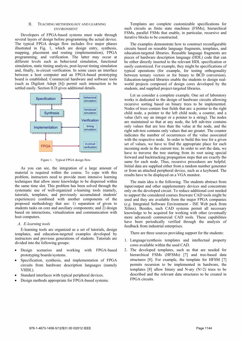
Developers of FPGA-based systems must wade through several layers of design before programming the actual device. The typical FPGA design flow includes five major phases illustrated in Fig. 1, which are design entry, synthesis, mapping, placement and routing (implementation), FPGA programming, and verification. The latter may occur at different levels such as behavioral simulation, functional simulation, static timing analysis, post-layout timing simulation and, finally, in-circuit verification. In some cases an interface between a host computer and an FPGA-based prototyping board is established. Commercial hardware and software tools (such as Digilent Adept [6]) permit such interaction to be settled easily. Section II.D gives additional details.
SpecificationSpecification
VerificationVerification
ImplementationImplementation
FPGA
SynthesisSynthesis
behavioralsimulation
functionalsimulation
timingsimulation
in-circuitverification
Figure 1. Typical FPGA design flow.
As you can see, the integration of a large amount of material is required within the course. To cope with this problem, instructors need to provide more intensive learning techniques that allow more knowledge to be dispersed within the same time slot. This problem has been solved through the systematic use of well-organized e-learning tools (namely, tutorials, templates, and previously accumulated students' experiences) combined with another components of the proposed methodology that are: 1) separation of given to students tasks on core and auxiliary components; and 2) design based on interactions, virtualization and communication with host computers.
A. E-learning tools
E-learning tools are organized as a set of tutorials, design templates, and education-targeted examples developed by instructors and previous generations of students. Tutorials are divided into the following groups:
Design scenarios and working with FPGA-based prototyping boards/systems.
Specification, synthesis, and implementation of FPGA circuits from hardware description languages (namely VHDL).
Standard interfaces with typical peripheral devices. Design methods appropriate for FPGA-based systems.
Templates are complete customizable specifications for such circuits as finite state machines (FSMs), hierarchical FSMs, parallel FSMs that enable, in particular, recursive and iterative blocks to be constructed.
The examples demonstrate how to construct reconfigurable circuits based on reusable language fragments, templates, and education-targeted libraries. Reusable language fragments are pieces of hardware description language (HDL) code that can be either directly inserted to the relevant HDL specification or easily customized. For example, they might be specifications of typical operations (for example, for testing orthogonality between ternary vectors or for binary to BCD conversion). Education-targeted libraries enable the students to design real-world projects composed of design cores developed by the students, and supplied project-targeted libraries.
Let us consider a complete example. One set of laboratory works is dedicated to the design of hardware circuits allowing recursive sorting based on binary trees to be implemented. Nodes of trees contain four fields that are: a pointer to the right child node, a pointer to the left child node, a counter, and a value (let's say an integer or a pointer to a string). The nodes are maintained so that at any node, the left sub-tree contains only values that are less than the value at the node, and the right sub-tree contains only values that are greater. The counter indicates the number of occurrences of the value associated with the respective node. In order to build this tree for a given set of values, we have to find the appropriate place for each incoming node in the current tree. In order to sort the data, we have to traverse the tree starting from its root using special forward and backtracking propagation steps that are exactly the same for each node. Thus, recursive procedures are helpful. Initial data are supplied either from a random number generator or from an attached peripheral device, such as a keyboard. The results have to be displayed on a VGA monitor.
The main idea is the following. The students abstract from input/output and other supplementary devices and concentrate only on the developed circuit. To reduce additional cost needed to support the considered courses freeware CAD tools might be used and they are available from the major FPGA companies (e.g. Integrated Software Environment - ISE Web pack from Xilinx). Besides, such CAD systems permit all necessary knowledge to be acquired for working with other (eventually more advanced) commercial CAD tools. These capabilities have been periodically verified through the analysis of feedback from industrial enterprises.
There are three sources providing support for the students:
1. Language/synthesis templates and intellectual property cores available within the used CAD.
2. The developed templates, such as that are needed for hierarchical FSMs (HFSMs) [7] and tree-based data structures [8]. For example, the template for HFSM [7] permits recursion to be implemented in hardware, the templates [8] allow binary and N-ary (N>2) trees to be described and the relevant data structures to be created in FPGA circuits.
978-1-4673-1456-5/12/$31.00 ©2012 IEEE Page 1144
3. Reusable components developed by previous generations of students, such as that provide support for different peripheral devices (e.g. communications through wireless Bluetooth [9] and RF [10] interfaces), data processing [8], priority management [11], etc.
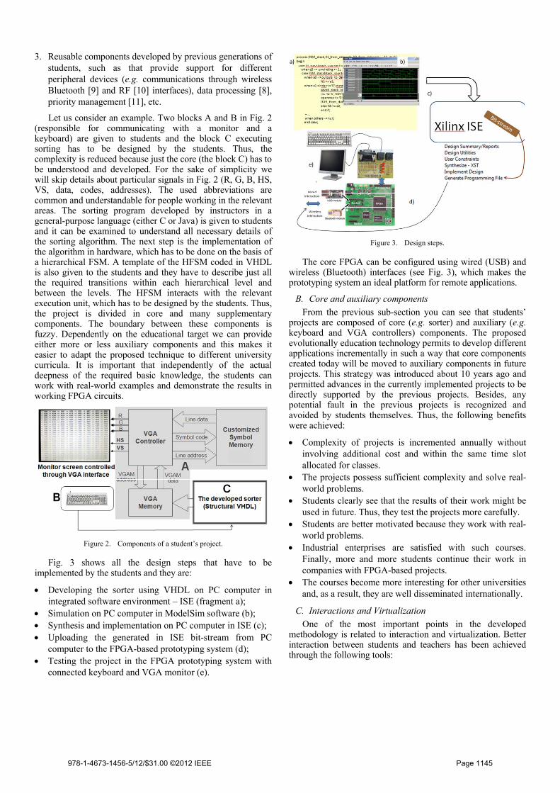
Let us consider an example. Two blocks A and B in Fig. 2 (responsible for communicating with a monitor and a keyboard) are given to students and the block C executing sorting has to be designed by the students. Thus, the complexity is reduced because just the core (the block C) has to be understood and developed. For the sake of simplicity we will skip details about particular signals in Fig. 2 (R, G, B, HS, VS, data, codes, addresses). The used abbreviations are common and understandable for people working in the relevant areas. The sorting program developed by instructors in a general-purpose language (either C or Java) is given to students and it can be examined to understand all necessary details of the sorting algorithm. The next step is the implementation of the algorithm in hardware, which has to be done on the basis of a hierarchical FSM. A template of the HFSM coded in VHDL is also given to the students and they have to describe just all the required transitions within each hierarchical level and between the levels. The HFSM interacts with the relevant execution unit, which has to be designed by the students. Thus, the project is divided in core and many supplementary components. The boundary between these components is fuzzy. Dependently on the educational target we can provide either more or less auxiliary components and this makes it easier to adapt the proposed technique to different university curricula. It is important that independently of the actual deepness of the required basic knowledge, the students can work with real-world examples and demonstrate the results in working FPGA circuits.
Figure 2. Components of a student’s project.
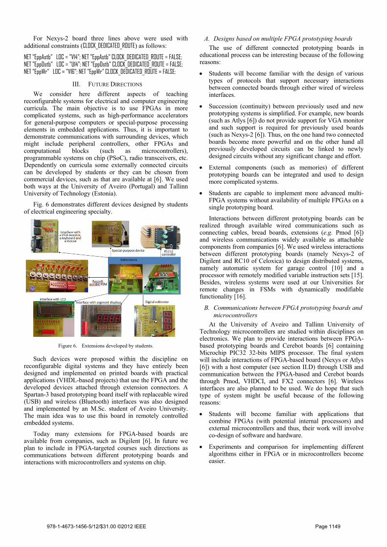
Fig. 3 shows all the design steps that have to be implemented by the students and they are:
Developing the sorter using VHDL on PC computer in integrated software environment – ISE (fragment a);
Simulation on PC computer in ModelSim software (b); Synthesis and implementation on PC computer in ISE (c); Uploading the generated in ISE bit-stream from PC
computer to the FPGA-based prototyping system (d); Testing the project in the FPGA prototyping system with
connected keyboard and VGA monitor (e).
Figure 3. Design steps.
The core FPGA can be configured using wired (USB) and wireless (Bluetooth) interfaces (see Fig. 3), which makes the prototyping system an ideal platform for remote applications.
B. Core and auxiliary components
From the previous sub-section you can see that students’ projects are composed of core (e.g. sorter) and auxiliary (e.g. keyboard and VGA controllers) components. The proposed evolutionally education technology permits to develop different applications incrementally in such a way that core components created today will be moved to auxiliary components in future projects. This strategy was introduced about 10 years ago and permitted advances in the currently implemented projects to be directly supported by the previous projects. Besides, any potential fault in the previous projects is recognized and avoided by students themselves. Thus, the following benefits were achieved:
Complexity of projects is incremented annually without involving additional cost and within the same time slot allocated for classes.
The projects possess sufficient complexity and solve real-world problems.
Students clearly see that the results of their work might be used in future. Thus, they test the projects more carefully.
Students are better motivated because they work with real-world problems.
Industrial enterprises are satisfied with such courses. Finally, more and more students continue their work in companies with FPGA-based projects.
The courses become more interesting for other universities and, as a result, they are well disseminated internationally.
C. Interactions and Virtualization
One of the most important points in the developed methodology is related to interaction and virtualization. Better interaction between students and teachers has been achieved through the following tools:
978-1-4673-1456-5/12/$31.00 ©2012 IEEE Page 1145

Interactive white board 680i of Smart Technologies communicating with HP Elite Book tablet PCs 2730p;
Extensive graphical capabilities of tablet PCs 2730p equipped with an electronic pen for hand writing;
Availability of tablet PCs with installed FPGA-targeted software both inside and outside the class rooms;
Remote access to all supplementary materials discussed in the previous section (tutorials, templates, projects of previous students) that are centralized in course-oriented web pages;
Continuous (step by step) evaluation procedure, which forces the students to learn and clearly understand all important topics before each new class;
Optional evaluation procedure through individual projects, which are proposed at the beginning and have to be completed before the end of a semester. This strategy motivates student to work in FPGA-targeted areas.
We found that the interactive white board is extremely useful when we need to present many important details within limited time slots. Indeed, you can demonstrate design steps on the board visible to all students in the class room much similar as you can do it on your personal computer. At any time students can copy to their computers a screenshot from the board for future studying, reminder, and reference. They can send electronically questions and even hand drawn fragments of circuits that can later be shown on the board and explained by the teacher or simulated using the installed software. The fragments with explanations (including teacher’s remarks) might be sent back to the students if required. Numerous tools, such as magnifying, selection, attracting attention to a particular point, are very helpful.
Virtualization enables real-world problems to be implemented and tested without additional cost and equipment. The developed system is considered to be partially implemented in software of the host computer and partially in hardware of the FPGA-based prototyping board. The software/hardware parts interact through an interface and they are assembled in such a way that we can explore systems with either more hardware or more software. In other words the boundary between software and hardware is rather flexible. For example, a large number of available FPGA-based prototyping systems make it difficult to find the best choice and, as a rule, it is necessary to achieve a compromise between the required hardware/software resources and the price. Taking into account the fact that the majority of prototyping boards/systems include many typical components (such as memories, liquid crystal displays - LCDs, standard interfaces, etc.) it is very difficult to find a board optimally targeted to the particular application, i.e. such a board that contains only those elements that are required for a particular student problem and no other components, which just increase the cost and occupy the space.
One possible solution to overcome this problem can be achieved through the design of an extendable set of hardware/software tools easily retargeted to different engineering application areas [9]. Any particular problem can be solved using just the required subset from the considered set, which includes only the needed hardware/software
components and excludes all the other available components. In case if the desired components are not available they can be constructed easily. The design process is divided into two stages. The first stage is verification and debugging of the developed application at different levels of abstraction, namely:
Simulation in computer using general-purpose and application-specific software;
Hardware/software co-simulation in such a way that the developed FPGA-based circuits interact with a virtual system displayed on a monitor screen and the considered virtual system is supported by the relevant software models (see Fig. 4).
Hardware libraries that enable the designers to communicate with typical peripheral devices (see the right-hand part of Fig. 4). This is very helpful for the design of real-world applications in education.
Figure 4. Physical and virtual interfaces with the prototyping board.
After the developed FPGA-based system has been tested it can be connected to the proper physical system. At this stage we can use the same prototyping board replacing USB interface block with Bluetooth wireless interface block, which can be inserted in the same socket [12] (see Fig. 3,e). After that we still have support for debugging through remote interactions. This permits many useful functions to be implemented, such as:
Reading and verifying the system’s intermediate states; Remote reconfiguration; Intellectual assistance from the host computer, which
evidently possesses more powerful hardware/software resources;
Virtual capabilities that allow the circuit to be constructed on an FPGA that does not have sufficient hardware resources to accommodate all the required functionality;
Remote interactions with FPGA-based systems enabling adaptation and virtualization to be provided.
The developed methods and tools are portable and thus, they can be used in different universities and section IV demonstrates particular steps in such activity.
978-1-4673-1456-5/12/$31.00 ©2012 IEEE Page 1146

D. Communication with host computer
Nowadays there are many FPGA-based prototyping boards available for education purposes. Some of them, such as DE2-115 of Altera [13], contain many onboard components for interaction with the user. Other systems, such as Atlys of Digilent [6], have just a few pushbuttons, leds, and dipswitches. As a rule, instructors propose projects requiring significantly more extensive exchange of data. Fortunately, available software tools (such as Digilent Adept [6]) allow virtual components displayed on a monitor screen of a host PC to be used for interactions.
Let us consider an example of the following VHDL code allowing division operation between two size_of_operands-bit integers to be executed. The results are produced in form of a quotient and a remainder using the know division algorithm [14].
entity MyDivider is generic (size_of_operands : integer := 8 ); Port ( clk : in std_logic; rst : in std_logic; Divident : in std_logic_vector(size_of_operands-1 downto 0); Divisor : in std_logic_vector(size_of_operands-1 downto 0); Quotient : out std_logic_vector(size_of_operands-1 downto 0); Remainder : out std_logic_vector(size_of_operands-1 downto 0); divide_by_zero : out std_logic ); end MyDivider; architecture Behavioral of MyDivider is
type state_type is (a0,a1,a2,a3,a4,a5); signal FSMstate, FSMnext_state : state_type; signal local_quotient :
std_logic_vector(size_of_operands-1 downto 0) := (others => '0'); signal local_divisor :
std_logic_vector(2*size_of_operands-1 downto 0) := (others => '0');
begin
divide_by_zero <= '1' when Divisor = 0 else '0';
process(clk,rst) begin if rst = '1' then FSMstate <= a0; elsif falling_edge(clk) then FSMstate <= FSMnext_state; end if; end process;
process(clk) variable local_remainder : std_logic_vector(2*size_of_operands-1 downto 0) := (others => '0'); variable index : integer range 0 to size_of_operands+1 := 0; begin if rising_edge(clk) then case FSMstate is when a0 => FSMnext_state <= a1; local_quotient <= (others => '0'); local_divisor(2*size_of_operands-1 downto size_of_operands)
<= Divisor; local_remainder(size_of_operands-1 downto 0) := Divident; index := 0;
when a1 => if local_divisor > local_remainder then FSMnext_state <= a2; else FSMnext_state <= a3; end if; when a2 => FSMnext_state <= a4; local_quotient <= local_quotient(size_of_operands-2 downto 0) & '0'; when a3 => FSMnext_state <= a4;
local_remainder := local_remainder-local_divisor; local_quotient <= local_quotient(size_of_operands-2 downto 0) & '1'; when a4 => local_divisor <= '0' &
local_divisor(2*size_of_operands-1 downto 1); index := index+1; if (index = size_of_operands+1) then FSMnext_state <= a5; else FSMnext_state <= a1; end if; when a5 => FSMnext_state <= a0; Quotient <= local_quotient; Remainder <= local_remainder(size_of_operands-1 downto 0); when others => null; end case; else null; end if; end process;
end Behavioral;
Suppose we would like to work with 32-bit operands and, thus, size_of_operands=32. There are no sufficient on-board components allowing the circuit to be tested. However you can use virtual components of Adept [6] and the following VHDL code (generic statement permits the constant size_of_operands (equal to 32) to be supplied as a parameter to the divider with a default value 8):
entity Test_Divider is -- this code was tested for Digilent Atlys board generic ( size_of_operands : integer := 32 ); Port ( clk : in std_logic; -- signals below establish communication with Digilet VHDL module EppAstb : in std_logic; -- address strobe EppDstb : in std_logic; -- data strobe EppWr : in std_logic; -- port write signal EppDB : inout std_logic_vector(7 downto 0); -- port data bus EppWait : out std_logic; -- Port wait signal -- interaction with the divider BoardLed0 : out std_logic; -- indicates devide by zero BoardButton0 : in std_logic; -- used for reset BoardDip0 : in std_logic; -- permits either quotient -- (BoardDip0=’0’) or remainder (BoardDip0=’1’) to be sent to PC BoardDip7 : in std_logic ); -- permits to get from PC either -- dividend (BoardDip7=’0’) or divider (BoardDip7=’1’) end Test_Divider;
architecture Behavioral of Test_Divider is
component IOExpansion is -- link with Digilent component available at [6] Port ( EppAstb: in std_logic; -- address strobe EppDstb: in std_logic; -- data strobe EppWr : in std_logic; -- port write signal EppDB : inout std_logic_vector(7 downto 0); -- port data bus EppWait: out std_logic; -- port wait signal
978-1-4673-1456-5/12/$31.00 ©2012 IEEE Page 1147

-- user signals Led : in std_logic_vector(7 downto 0); -- 8 virtual LEDs on the PC LBar : in std_logic_vector(23 downto 0); -- 24 lights on the PC Sw : out std_logic_vector(15 downto 0); -- 16 switches on the PC Btn : out std_logic_vector(15 downto 0); -- 16 Buttons on the PC dwOut: out std_logic_vector(31 downto 0); -- 32 Bits user output dwIn : in std_logic_vector(31 downto 0) -- 32 Bits user input ); end component;
component MyDivider is generic ( size_of_operands : integer := size_of_operands ); Port ( clk : in std_logic; rst : in std_logic; Divident : in std_logic_vector (size_of_operands-1 downto 0); Divisor : in std_logic_vector (size_of_operands-1 downto 0); Quotient : out std_logic_vector (size_of_operands-1 downto 0); Remainder : out std_logic_vector (size_of_operands-1 downto 0); divide_by_zero: out std_logic ); end component;
signal MyLed : std_logic_vector(7 downto 0); -- connection with 8 -- virtual LEDs on the PC
signal MyLBar : std_logic_vector(23 downto 0); -- connection with 24 -- lights on the PC
signal MySw : std_logic_vector(15 downto 0); -- connection with 16 -- switches on the PC
signal MyBtn : std_logic_vector(15 downto 0); -- connection with 16 -- buttons on the PC
signal data_to_PC : std_logic_vector(31 downto 0); -- 32 bits user signal -- from FPGA to PC
signal data_from_PC : std_logic_vector(31 downto 0);-- 32 bits user signal -- from PC to FPGA
signal Q : std_logic_vector(size_of_operands-1 downto 0); -- quotient signal R : std_logic_vector(size_of_operands-1 downto 0); -- reminder signal divide_by_zero : std_logic; -- is equal to 1 in case of divide by 0 signal local_reset : std_logic; -- reset value is 1 signal Divident,Divisor : std_logic_vector(size_of_operands-1 downto 0);
begin
BoardLed0 <= divide_by_zero; -- Led 0 indicates divide by zero MyLBar <= MySw & MyBtn(15 downto 8); -- Virtual buttons and switches
-- are connected MyLed <= MyBtn(7 downto 0); -- with virtual indicators
process (clk) begin if rising_edge(clk) then if BoardDip7 = '0' then Divident <= data_from_PC; -- getting dividend and else Divisor <= data_from_PC; -- divisor from PC end if; if BoardDip0 = '0' then data_to_PC <= Q; -- sending to PC either resulting else data_to_PC <= R; -- quotient or remainder end if; end if; end process;
local_reset <= not BoardButton0; -- 0 value when pushbutton is pressed
IO_interface :IOExpansion portmap(EppAstb,EppDstb,EppWr,EppDB,EppWait,MyLed, MyLBar,MySw,MyBtn,data_from_PC,data_to_PC);
Divider : MyDivider generic map(size_of_operands=>size_of_operands) port map (clk, local_reset,Divident,Divisor,Q,R,divide_by_zero);
end Behavioral;
Now 32-bit operands (dividend and divider) can be entered from PC computer and a 32-bit result (quotient and remainder) can be displayed in a dialog box of Adept (see Fig. 5). Dependently on user-constraint file the code above can be tested in different prototyping boards (we used two boards of Digilent Nexys-2 with FPGA Spartan-3E-500 and Atlys with FPGA Spartan-6 XC6SLX45). For the Nexys-2 board the line local_reset <= BoardButton0; (without inversion not) has to be used.
If onboard switch 7 is off then data from Adept dialog window will be sent to FPGA register Divident else (i.e. switch 7 is on) to FPGA register Divisor (see VHDL code above). If onboard switch 0 is off then data sent to Adept dialog box represent quotient (Q in VHDL code above), else remainder (R in VHDL code above). Similarly many other simple circuits (e.g. binary to BCD converters and discovering the greatest common divisor) can be examined with operand sizes corresponding to real-world problems. Data exchange can also be provided between registers/memory of FPGA-based prototyping boards and software of a host computer. We tested many examples using C/C++ programs for such problems as operations over matrices (e.g. multiplication and addition), data sorting, etc.
FPGA‐based prototyping board
7 0DIP switches
Dividend from PC
Divider from PC
Quotient
RemainderUSB
Adept dialog window
Dividend and divisor
Quotient and
remainder
Figure 5. Data exchange between the FPGA-based prototyping board and a
host computer.
To simplify the use of the described above example we give below a user-constraint file for Atlys board [6].
NET "clk" LOC = "L15"; # system clock NET "BoardButton0" LOC = "T15"; # Button 0 NET "BoardLed0" LOC = "U18"; # Led 0 NET "BoardDip0" LOC = "A10"; # DIP switch 0 NET "BoardDip7" LOC = "E4"; # DIP switch 7 NET "EppAstb" LOC = "B9"; # interface through USB NET "EppDstb" LOC = "A9"; NET "EppWr" LOC = "C15"; NET "EppWait" LOC = "F13"; NET "EppDB<0>" LOC = "A2"; NET "EppDB<1>" LOC = "D6"; NET "EppDB<2>" LOC = "C6"; NET "EppDB<3>" LOC = "B3"; NET "EppDB<4>" LOC = "A3"; NET "EppDB<5>" LOC = "B4"; NET "EppDB<6>" LOC = "A4"; NET "EppDB<7>" LOC = "C5";
978-1-4673-1456-5/12/$31.00 ©2012 IEEE Page 1148
For Nexys-2 board three lines above were used with additional constraints (CLOCK_DEDICATED_ROUTE) as follows:
NET "EppAstb" LOC = "V14"; NET "EppAstb" CLOCK_DEDICATED_ROUTE = FALSE; NET "EppDstb" LOC = "U14"; NET "EppDstb" CLOCK_DEDICATED_ROUTE = FALSE; NET "EppWr" LOC = "V16"; NET "EppWr" CLOCK_DEDICATED_ROUTE = FALSE;
III. FUTURE DIRECTIONS
We consider here different aspects of teaching reconfigurable systems for electrical and computer engineering curricula. The main objective is to use FPGAs in more complicated systems, such as high-performance accelerators for general-purpose computers or special-purpose processing elements in embedded applications. Thus, it is important to demonstrate communications with surrounding devices, which might include peripheral controllers, other FPGAs and computational blocks (such as microcontrollers), programmable systems on chip (PSoC), radio transceivers, etc. Dependently on curricula some externally connected circuits can be developed by students or they can be chosen from commercial devices, such as that are available at [6]. We used both ways at the University of Aveiro (Portugal) and Tallinn University of Technology (Estonia).
Fig. 6 demonstrates different devices designed by students of electrical engineering specialty.
Figure 6. Extensions developed by students.
Such devices were proposed within the discipline on reconfigurable digital systems and they have entirely been designed and implemented on printed boards with practical applications (VHDL-based projects) that use the FPGA and the developed devices attached through extension connectors. A Spartan-3 based prototyping board itself with replaceable wired (USB) and wireless (Bluetooth) interfaces was also designed and implemented by an M.Sc. student of Aveiro University. The main idea was to use this board in remotely controlled embedded systems.
Today many extensions for FPGA-based boards are available from companies, such as Digilent [6]. In future we plan to include in FPGA-targeted courses such directions as communications between different prototyping boards and interactions with microcontrollers and systems on chip.
A. Designs based on multiple FPGA prototyping boards
The use of different connected prototyping boards in educational process can be interesting because of the following reasons:
Students will become familiar with the design of various types of protocols that support necessary interactions between connected boards through either wired of wireless interfaces.
Succession (continuity) between previously used and new prototyping systems is simplified. For example, new boards (such as Atlys [6]) do not provide support for VGA monitor and such support is required for previously used boards (such as Nexys-2 [6]). Thus, on the one hand two connected boards become more powerful and on the other hand all previously developed circuits can be linked to newly designed circuits without any significant change and effort.
External components (such as memories) of different prototyping boards can be integrated and used to design more complicated systems.
Students are capable to implement more advanced multi-FPGA systems without availability of multiple FPGAs on a single prototyping board.
Interactions between different prototyping boards can be realized through available wired communications such as connecting cables, bread boards, extensions (e.g. Pmod [6]) and wireless communications widely available as attachable components from companies [6]. We used wireless interactions between different prototyping boards (namely Nexys-2 of Digilent and RC10 of Celoxica) to design distributed systems, namely automatic system for garage control [10] and a processor with remotely modified variable instruction sets [15]. Besides, wireless systems were used at our Universities for remote changes in FSMs with dynamically modifiable functionality [16].
B. Communications between FPGA prototyping boards and microcontrollers
At the University of Aveiro and Tallinn University of Technology microcontrollers are studied within disciplines on electronics. We plan to provide interactions between FPGA-based prototyping boards and Cerebot boards [6] containing Microchip PIC32 32-bits MIPS processor. The final system will include interactions of FPGA-based board (Nexys or Atlys [6]) with a host computer (see section II.D) through USB and communication between the FPGA-based and Cerebot boards through Pmod, VHDCI, and FX2 connectors [6]. Wireless interfaces are also planned to be used. We do hope that such type of system might be useful because of the following reasons:
Students will become familiar with applications that combine FPGAs (with potential internal processors) and external microcontrollers and thus, their work will involve co-design of software and hardware.
Experiments and comparison for implementing different algorithms either in FPGA or in microcontrollers become easier.
978-1-4673-1456-5/12/$31.00 ©2012 IEEE Page 1149

Students will be capable to explore potential parallelism at different levels, namely: circuit level, using built-in soft (and for more advanced FPGAs hard) processing elements, and external microcontrollers.
For similar reasons we plan to implement systems, including FPGA and programmable systems on chip (PSoC) of Cypress.
C. Experiments with alternative and competitive FPGAs
Nowadays there are many companies, which fabricate FPGAs. Although it is difficult to acquire experience with all of them, we believe that knowledge in FPGAs of the most known two companies (namely Xilinx and Altera) should be provided. For such purposes we will suggest students to implement similar projects in Digilent Nexys/Atlys prototyping boards with Xilinx Spartan-3 and Spartan-6 FPGA [6] and Altera DE2-115 development kit [13] with Cyclone-IV 4C22 FPGA. Besides, we are planning to demonstrate some designs based on FX12 Board with Xilinx Virtex-4 FPGA, XUPV5-LX110T development system with Xilinx Virtex-5 XC5VLX110T FPGA [17], and Virtex-6 FPGA ML605 evaluation kit of Avnet [18]. This will give students all necessary knowledge to successfully work on design and implementation of reconfigurable systems.
IV. INTERNATIONAL COLLABORATION
At the beginning international collaboration was established between University of Aveiro (Portugal) and Tallinn University of Technology (Estonia). The first exchange of courses was done in 2008. Mutual benefits were achieved because expertise of both universities was combined and integrated. University of Aveiro has long-term experience in teaching FPGA-based systems and one group in Tallinn University of Technology is known in test and diagnostics of hardware circuits that are very important for FPGA-based design. In 2008 a short course in the scope of FPGA was given to students of Tallinn University of Technology in Estonia and a short course on testing was given to students of Aveiro University in Portugal.
From 2009 we agreed about common design tools and prototyping systems. They included:
The use of Digilent Spartan-3E and Spartan-6 prototyping systems (namely Nexys-2/3 and Atlys) [6];
The use of Xilinx Integrated Software Environment; The use of methods, tools and evolutionary strategy
described in section II. The use of common methods for the design of FPGA-
based digital systems [19-29]. Future use of common prototyping systems (for example,
in 2011 the same Spartan-6 prototyping boards were acquired and a decision was taken about experiments with a prototyping board DE2-115 of Altera [13]).
From 2009 to 2011 the courses were given annually. Finally, a Ph.D. student working in the scope of FPGA design under joint supervision began the work, which was presented in 14 international conferences, including FPL 2011, which is to our knowledge the largest in the world conference in the scope
of FPGAs and reconfigurable computing. On the 20th of January, 2012 the respective Ph.D thesis was successfully defended in Tallinn University of Technology.
Later on the results in teaching FPGA-based systems were presented in other universities listed at the beginning of the paper. A typical course in the scope of FPGA-based design is composed of three lectures and subsequent practical classes given to students within one week. The lectures are dedicated to:
Lecture 1: Introduction, schematic design, behavioral HDL-based design; linking modules; structural HDL-based design; creating and using libraries.
Lecture 2: Auxiliary blocks for interaction with peripheral devices and host computers. Design of core components based on examples of arithmetic circuits.
Lecture 3: Real world examples, such as recursive sorting algorithms using a hierarchical finite state machine model.
V. RESULTS
In order to evaluate the proposed methodology, in a period of three years we have analyzed the following three characteristics:
Average complexity of the projects proposed to the students;
The level of students’ knowledge required to implement the projects;
Time spent by the students to implement the projects.
Analysis of characteristics considered above was done by teachers responsible for FPGA-targeted disciplines.
The main impact from the proposed methodology and the project [5] can be summarized as follows:
The students spent more time working on computers. Interactions between the students and teachers were
significantly improved. The complexity of students’ projects and the level of the
required students’ knowledge were increased.
Many improvements become possible due to wider accessibility of previously and newly developed methods and tools, better motivation, and easier interactions between both “teachers – students” and “current students - previous students”. This result can be obtained thanks to the proposed evolutional strategy described in section II. Available photo and video equipment has permitted useful presentations to be recorded and posted online. The presentations were done by both former students and teachers.
Some projects on which the students have been working recently are listed below (all these projects are relatively complicated and have been finally implemented and tested in FPGAs):
Receiver for optical transport network; Reconfigurable digital audio mixer for electro acoustic
music;
978-1-4673-1456-5/12/$31.00 ©2012 IEEE Page 1150
Sorting algorithms mapped to hardware and implemented on the basis of embedded Power PC processors;
Implementation of recursive sorting algorithms based on HFSM models;
Reconfigurable architectures for problems of combinatorial optimization;
Methods and tools for remote configuration of FPGAs; Urban traffic control simulation and evaluation platform; Automatic garage control and virtual simulation; Library for interaction with peripheral equipment.
The results of the projects clearly demonstrate importance of FPGAs for education targeted to different areas. In conclusion we would like to consider two examples from the list above with more details.
The first example is a networked embedded system for garage control and virtual simulation described in [10]. The system is organized as a composition of sub-systems communicating through established wired or wireless interfaces. One sub-system is responsible for the entire garage, i.e. for the set of such operations as: processing and indication of the most preferable parking slots, instructing the cars that enter the garage or have to be retrieved, etc. This subsystem was implemented on the basis of Celoxica RC10 prototyping board. Other sub-systems (implemented in Nexys-2 prototyping board) are installed inside cars and they drive cars without people to the slots selected by the first sub-system.
Any incoming car is stopped in front of the entrance gate where there is an eventual queue. A driver leaves the car and then the automatic system is responsible for further steps of parking. As soon as a free parking slot appears, the entrance door is opened and the central sub-system instructs the car how to drive to the designated parking slot. Requests for retrieving cars from the garage are formed by car owners. The chosen car drives automatically to the exit gate (according to the instructions given by the central sub-system), avoiding all potential obstacles, and then is parked in a place where the car owner waits. Fig. 7 demonstrates the idea of FPGA-based virtual simulation. Video presentation of a simulation scenario is available online [30].
Figure 7. Implementation of FPGA-based embedded system (a) and virtual
simulation (b).
Communication between the sub-systems is provided either in an emulation mode (within the same FPGA) or through RF wireless interface as it is shown in Fig. 7,a. Functionality of the system is demonstrated virtually on a monitor screen in
accelerating time (see Fig. 7,b) allowing many potential problems to be discovered visually. All necessary details can be found in [10]. The work was completely done by one student during about eight months.
The second example is dedicated to FPGA-based application for evaluation of urban traffic systems. It is assumed that road maps within a city are taken somehow (for instance, from Google), appended by traffic lights, and displayed on a monitor screen in such a way that is shown in Fig. 8 (the traffic lights are indicated by numbers and can be magnified and displayed explicitly if needed).
Figure 8. FPGA virtual simulation of an urban traffic system.
At the next step a number of cars can be introduced. Many parameters (e.g. car speed, traffic light times) can be changed dynamically. Thus, we are capable to visually check potential deadlocks, incorrect functionality of traffic light controllers, etc. The work was entirely done by one student and implemented within a single FPGA chip during about eight months [31]. Video presentation of a simulation scenario is available online [32].
Thus, we can see applicability of FPGAs in different areas. Even more sophisticated applications can be found in bioinformatics [33], medical instruments [34], information and communication [24] and other areas. Wide multidisciplinary scope gives additional motivation to include FPGA-targeted disciplines in engineering curricula. Existing forecasts indicate extension of FPGA-based applications in future.
VI. CONCLUSION
Analysis of students’ results and outcomes of international collaboration prove that the proposed methodology for teaching reconfigurable (FPGA-based) systems is very promising and can be recommended for future dissemination. In particular this methodology permits: 1) real-world problems to be addressed without involving new resources and with low supplementary cost; 2) achieve better motivation of students; 3) increase interest of industrial companies and the respective employment rate; 4) establish better links between FPGA-targeted and other disciplines; 5) expect further extension of international collaboration.
978-1-4673-1456-5/12/$31.00 ©2012 IEEE Page 1151

ACKNOWLEDGMENTS
This research was supported by HP grant award “Use of HP Mobile Technology to Enhance Teaching Reconfigurable Systems for Electrical and Computer Engineering Curricula”, the European Union through the European Regional Development Fund, the Estonian Science Foundation (Grant 9251), ERASMUS program, FEDER through the Operational Program Competitiveness Factors - COMPETE and by National Funds through FCT - Foundation for Science and Technology in the context of project FCOMP-01-0124-FEDER-022682 (FCT reference PEst-C/EEI/UI0127/2011).
REFERENCES [1] The Education, Audiovisual and Culture Executive Agency, Erasmus
Mundus Programme, available at: http://eacea.ec.europa.eu/erasmus_mundus/programme/about_erasmus_mundus_en.php.
[2] M. Santarini, “Zynq-7000 EPP Sets Stage for New Era of Innovations”, Xcell journal, issue 75, second quarter, 2011.
[3] World’s Highest Capacity FPGA - Now Shipping (25 October, 2011), available at: http://www.xilinx.com/products/silicon-devices/fpga/virtex-7/.
[4] V. Sklyarov and I. Skliarova, "Teaching Reconfigurable Systems: Methods, Tools, Tutorials and Projects", IEEE Transactions on Education, vol. 48, no. 2, May 2005, pp. 290-300.
[5] Information on the project “Use of HP Mobile Technology to Enhance Teaching Reconfigurable Systems for Electrical and Computer Engineering Curricula”, available at: http://www.ieeta.pt/~skl/HP_project.html.
[6] Digilent Inc., Products, available at: http://www.digilentinc.com.
[7] V. Sklyarov, “Synthesis of Circuits and Systems from Hierarchical and Parallel Specifications”, Proc. of the 12th Biennial Baltic Electronics Conference - BEC 2010, invited paper, Tallinn, Estonia, 2010, pp. 37-48.
[8] D. Mihhailov, A. Sudnitson, V. Sklyarov, I. Skliarova, "Acceleration of Recursive Data Sorting over Tree-based Structures", Electronics and Electrical Engineering, Kaunas, ISSN 1392 – 1215, 2011, N7 (113), pp. 51–56.
[9] V. Sklyarov, I. Skliarova, B. Pimentel, and M. Almeida, "Multimedia Tools and Architectures for Hardware/Software Co-Simulation of Reconfigurable Systems", Proc. of the 21st International Conference on VLSI Design – VLSI Design’2008, Hyderabad, India, January 2008, pp. 85-90.
[10] V. Sklyarov, I. Skliarova, and A. Neves, "Modeling and Implementation of Automatic System for Garage Control", Proc. of ICROS-SICE International Joint Conference – ICCAS-SICE’2009, Fukuoka, Japan, August 2009, pp. 4295-4300.
[11] V. Sklyarov and I. Skliarova, "Modeling, Design, and Implementation of a Priority Buffer for Embedded Systems", Proc. of the 7th Asian Control Conference – ASCC’2009, Hong Kong, August 2009, pp. 9-14.
[12] M. Almeida, V. Sklyarov, I. Skliarova, and B. Pimentel, "Design Tools for Reconfigurable Embedded Systems", Proc. of the 2nd International Conference on Embedded Software and Systems - ICESS'2005, IEEE Computer Society, Xi'an, December 2005, pp. 254-261.
[13] Altera, DE2-115 Development and Education Board, available at: http://www.altera.com/education/univ/materials/boards/de2-115/unv-de2-115-board.html.
[14] D.A. Patterson and J.L. Hennessy, Computer Organization and Design, Morgan Kaufmann Publishers, 2009.
[15] V. Sklyarov, I. Skliarova, and J. Lima, "Design and Implementation of Communicating Fixed and Variable Instruction Set Processors", Proc. of the 2nd International Conference on Computer and Electrical Engineering - ICCEE 2009, Dubai, UAE, December 2009, pp. 163-167.
[16] V. Sklyarov, “Reconfigurable models of finite state machines and their implementation in FPGAs”, Journal of Systems Architecture, 47, 2002, pp. 1043-1064.
[17] Xilinx University Program XUPV5-LX110T Development System, available at: http://www.xilinx.com/univ/xupv5-lx110t.htm.
[18] Xilinx, Virtex-6 FPGA ML605 Evaluation Kit, available at: http://www.xilinx.com/products/boards-and-kits/EK-V6-ML605-G.htm.
[19] V. Sklyarov and I. Skliarova, "Recursive and Iterative Algorithms for N-ary Search Problems", International Federation for Information Processing, vol. 218, 2nd IFIP Symposium on Professional Practice in Artificial Intelligence - AISPP'2006, ed. J. Debenham, 19th IFIP World Computer Congress - WCC'2006, Santiago de Chile, Chile, Aug. 2006, pp. 81-90.
[20] D. Mihhailov, V. Sklyarov, I. Skliarova, and A. Sudnitson, "Hardware Implementation of Recursive Algorithms", Proc. of the 2010 IEEE International 53rd Midwest Symposium on Circuits and Systems - MWSCAS 2010, Seattle, USA, August 2010, pp. 225-228.
[21] V.Sklyarov, Synthesis of Finite State Machines Based on Matrix LSI, Science, Minsk, Belarus, 1984.
[22] V. Sklyarov and I. Skliarova, "Design and Implementation of Parallel Hierarchical Finite State Machines", Proc. of the 2nd International Conference on Communications and Electronics – HUT-ICCE’2008, Hoi An, Vietnam, June 2008, pp. 33-38.
[23] V. Sklyarov, I. Skliarova, P. Almeida, and M. Almeida, "Design Tools and Reusable Libraries for FPGA-Based Digital Circuits", Proc. of the EUROMICRO Symposium on Digital System Design - DSD'2003, Antalya, Turkey, September 2003, pp. 255-263.
[24] V. Sklyarov, I. Skliarova, and A. Sudnitson, "FPGA-based Systems in Information and Communication", tutorial, Proc. of the 5th International Conference on Application of Information and Communication Technologies - AICT'2011, Baku, Azerbaijan, October 2011, pp. 551-555.
[25] V. Sklyarov, I. Skliarova, D. Mihhailov, and A. Sudnitson, "Implementation in FPGA of Address-based Data Sorting", Proc. of the 21st International Conference on Field-Programmable Logic and Applications - FPL 2011, Crete, Greece, September 2011, pp. 405-410.
[26] D. Mihhailov, V. Sklyarov, I. Skliarova, and A. Sudnitson, "Parallel FPGA-based Implementation of Recursive Sorting Algorithms", Proc. of the 2010 International Conference on ReConFigurable Computing and FPGAs - ReConFig 2010, Cancun, Mexico, December 2010, pp. 121-126.
[27] V. Sklyarov and I. Skliarova, "Architecture of a Reconfigurable Processor for Implementing Search Algorithms over Discrete Matrices", Proc. of the International Conference on Engineering of Reconfigurable Systems and Algorithms - ERSA'2003, Las Vegas, USA, June 2003, pp. 127-133.
[28] V. Sklyarov, I. Skliarova, and A.B. Ferrari, "Hierarchical Specification and Implementation of Combinatorial Algorithms Based on RHS Model", Proc. of the XVI Conference on Design of Circuits and Integrated Systems - DCIS'2001, Oporto, Portugal, November 2001, pp. 486-491.
[29] V. Sklyarov and I. Skliarova, "Design of Digital Circuits on the Basis of Hardware Templates", Proc. of the International Conference on Embedded Systems and Applications - ESA'2003, H.R. Arabnia, L.T. Yang (eds.), Las Vegas, USA, June 2003, pp. 56-62.
[30] Video presentation of simulation of FPGA-based garage control system, available at: www.ieeta.pt/~skl/GarageControl.wmv.
[31] S. Soldado, “FPGA Urban Traffic Control Simulation and Evaluation Platform”, M.Sc. thesis, University of Aveiro, 2008, available at: http://www.ieeta.pt/~skl/Research/From2008/MSc/Sergio.pdf.
[32] Video presentation of simulation of urban traffic system, available at: http://www.ieeta.pt/~skl/UrbanControl.wmv.
[33] S. Sarkar, T. Majumder, A. Kalyanaraman, and P.P. Pande, ”Hardware Accelerators for Biocomputing: A Survey”, Proc. of 2010 IEEE International Symposium on Circuits and Systems – ISCAS, Paris, France, 2010, pp. 3789-3792.
[34] M. Jenihhin, M. Gorev, V. Pesonen, D. Mihhailov, P. Ellervee, H. Hinrikus, M. Bachmann, and J. Lass, “EEG Analyzer Prototype Based on FPGA”, Proc. of the 7th Int. Symp. on Image and Signal Processing and Analysis - ISPA, Dubrovnik, Croatia, 2011, pp. 101-106.
978-1-4673-1456-5/12/$31.00 ©2012 IEEE Page 1152