Embed Size (px)
Citation preview
MEMS/NEMS approaches
for energy harvesting
István BÁRSONY and János VOLK
Research Institute for Technical Physics and Materials Science (MFA)Hungarian Academy of Sciences
Budapest, Hungary
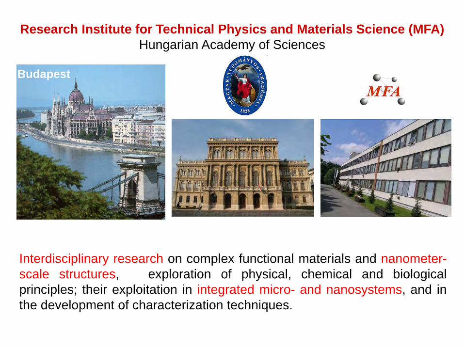
Interdisciplinary research on complex functional materials and nanometer-scale structures, exploration of physical, chemical and biologicalprinciples; their exploitation in integrated micro- and nanosystems, and inthe development of characterization techniques.
Research Institute for Technical Physics and Materials Science (MFA)Hungarian Academy of Sciences
Budapest
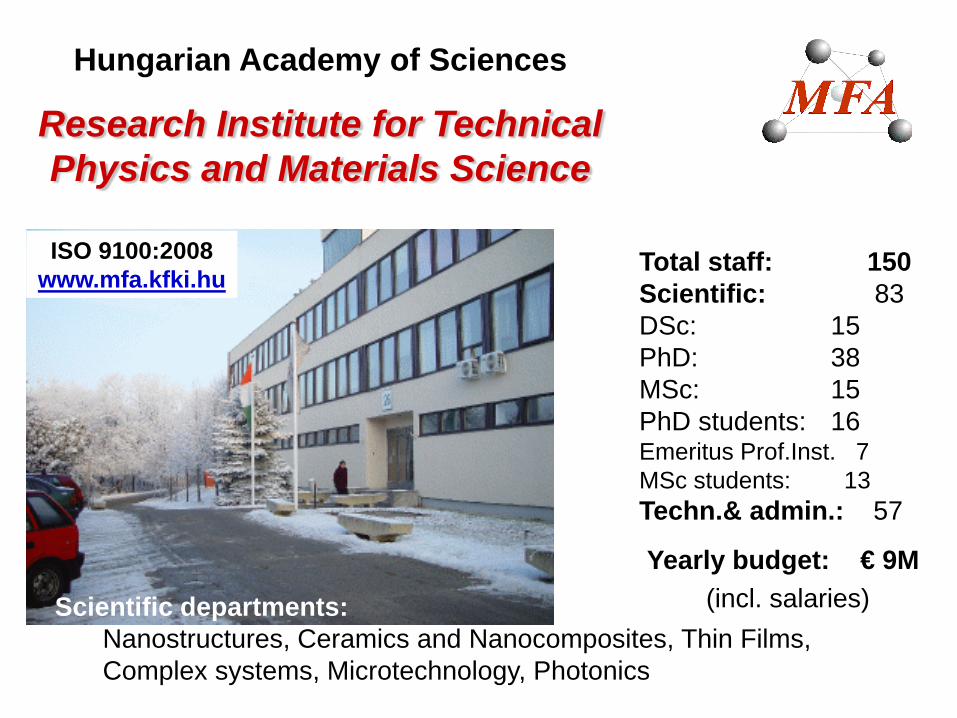
Hungarian Academy of Sciences
Research Institute for Technical Physics and Materials Science
ISO 9100:2008www.mfa.kfki.hu
Total staff: 150Scientific: 83 DSc: 15 PhD: 38 MSc: 15PhD students: 16Emeritus Prof.Inst. 7MSc students: 13Techn.& admin.: 57
Yearly budget: € 9M(incl. salaries)Scientific departments:
Nanostructures, Ceramics and Nanocomposites, Thin Films, Complex systems, Microtechnology, Photonics
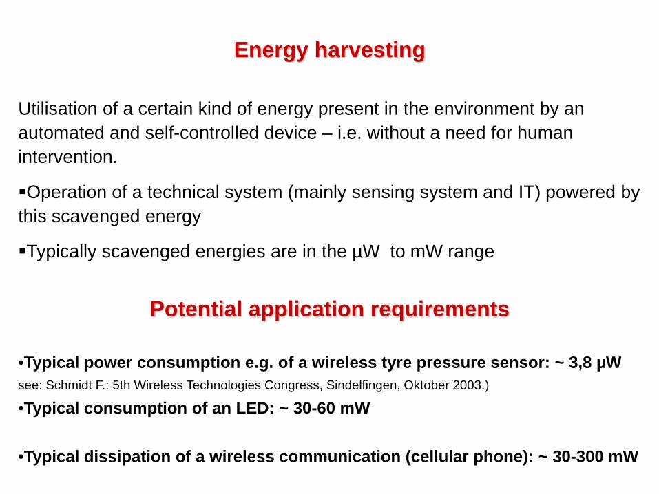
Energy harvesting
Utilisation of a certain kind of energy present in the environment by an automated and self-controlled device – i.e. without a need for human intervention.
Operation of a technical system (mainly sensing system and IT) powered bythis scavenged energy
Typically scavenged energies are in the µW to mW range
Potential application requirements
•Typical power consumption e.g. of a wireless tyre pressure sensor: ~ 3,8 µWsee: Schmidt F.: 5th Wireless Technologies Congress, Sindelfingen, Oktober 2003.)
•Typical consumption of an LED: ~ 30-60 mW
•Typical dissipation of a wireless communication (cellular phone): ~ 30-300 mW
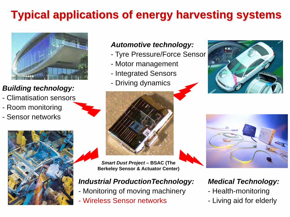
Typical applications of energy harvesting systems
Automotive technology:- Tyre Pressure/Force Sensor- Motor management- Integrated Sensors- Driving dynamics
Medical Technology:- Health-monitoring- Living aid for elderly
Building technology:- Climatisation sensors- Room monitoring- Sensor networks
Smart Dust Project – BSAC (The Berkeley Sensor & Actuator Center)
Industrial ProductionTechnology:- Monitoring of moving machinery- Wireless Sensor networks
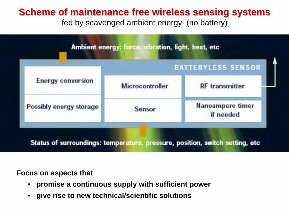
Scheme of maintenance free wireless sensing systems fed by scavenged ambient energy (no battery)
Focus on aspects that• promise a continuous supply with sufficient power• give rise to new technical/scientific solutions
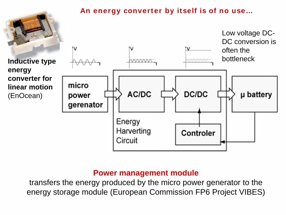
Inductive type energy converter for linear motion(EnOcean)
Power management moduletransfers the energy produced by the micro power generator to the
energy storage module (European Commission FP6 Project VIBES)
Low voltage DC-DC conversion is often the bottleneck
An energy converter by itself is of no use…
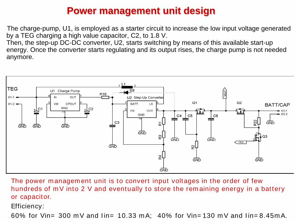
Power management unit designThe charge-pump, U1, is employed as a starter circuit to increase the low input voltage generated by a TEG charging a high value capacitor, C2, to 1.8 V. Then, the step-up DC-DC converter, U2, starts switching by means of this available start-up energy. Once the converter starts regulating and its output rises, the charge pump is not needed anymore.
The power management unit is to convert input voltages in the order of few hundreds of mV into 2 V and eventually to store the remaining energy in a battery or capacitor.Efficiency: 60% for Vin= 300 mV and Iin= 10.33 mA; 40% for Vin=130 mV and Iin=8.45mA.
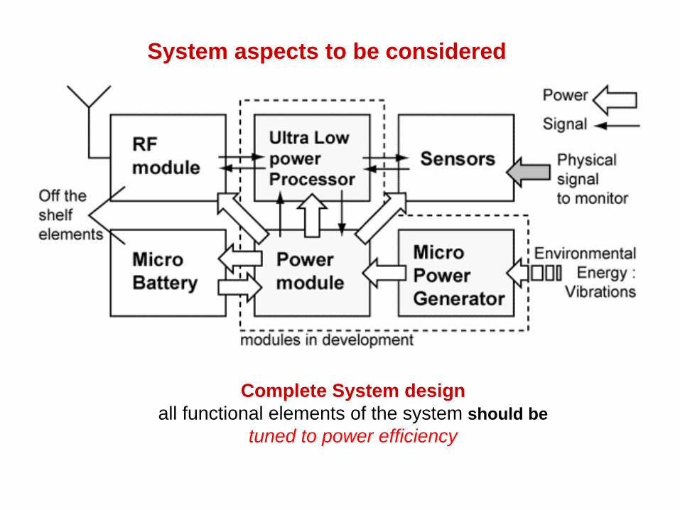
Complete System designall functional elements of the system should be
tuned to power efficiency
System aspects to be considered
Operation:
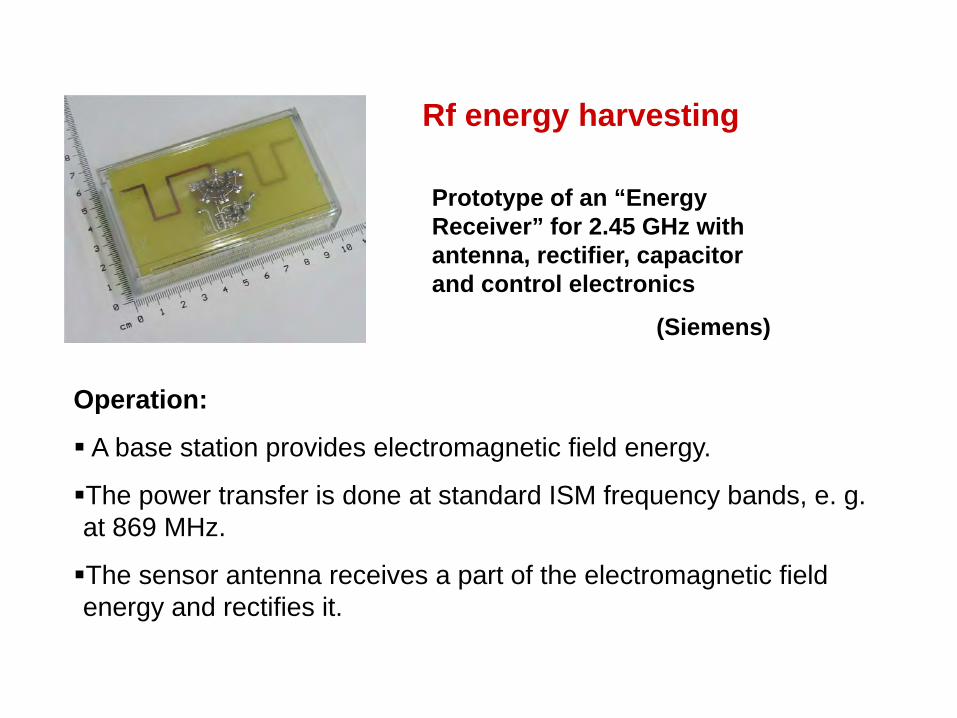
A base station provides electromagnetic field energy.
The power transfer is done at standard ISM frequency bands, e. g. at 869 MHz.
The sensor antenna receives a part of the electromagnetic field energy and rectifies it.
Rf energy harvesting
Prototype of an “Energy Receiver” for 2.45 GHz with antenna, rectifier, capacitor and control electronics
(Siemens)
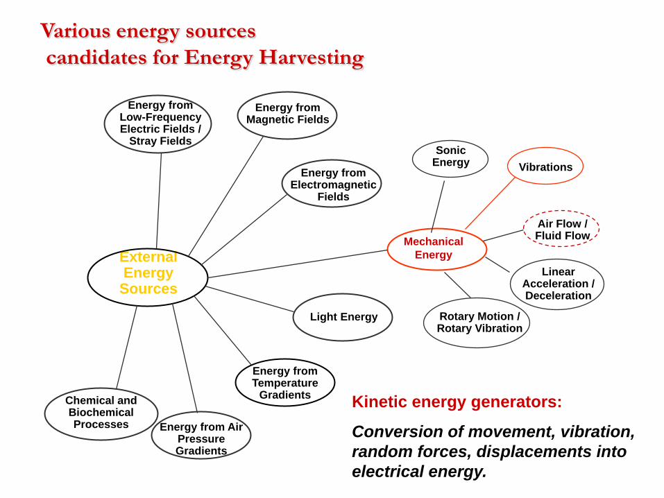
External Energy Sources
Chemical and Biochemical Processes
Energy from Magnetic Fields
Vibrations
Air Flow / Fluid Flow
Sonic Energy
Energy from Electromagnetic
Fields
Energy from Temperature
Gradients
Energy from Air Pressure Gradients
Mechanical Energy
Light Energy
Linear Acceleration / Deceleration
Rotary Motion / Rotary Vibration
Energy from Low-Frequency Electric Fields /
Stray Fields
Various energy sources candidates for Energy Harvesting
Kinetic energy generators:
Conversion of movement, vibration, random forces, displacements into electrical energy.
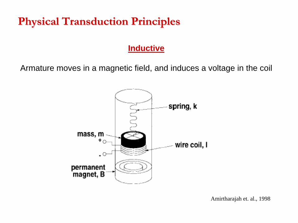
Physical Transduction Principles
Inductive
Armature moves in a magnetic field, and induces a voltage in the coil
Amirtharajah et. al., 1998
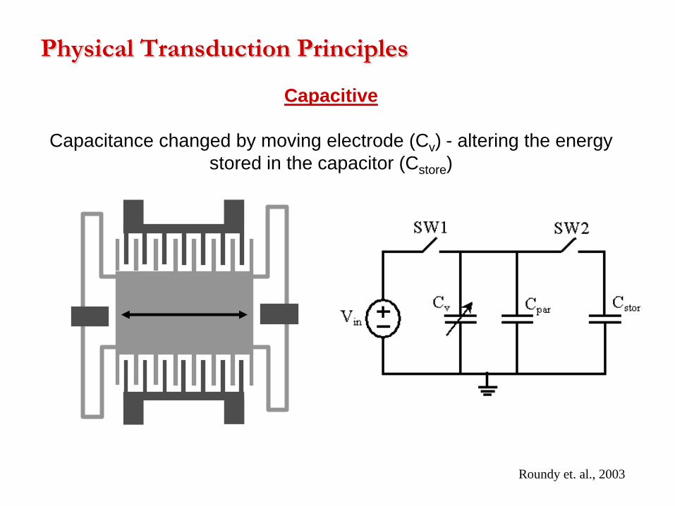
Physical Transduction Principles
Capacitive
Capacitance changed by moving electrode (Cv) - altering the energystored in the capacitor (Cstore)
Roundy et. al., 2003
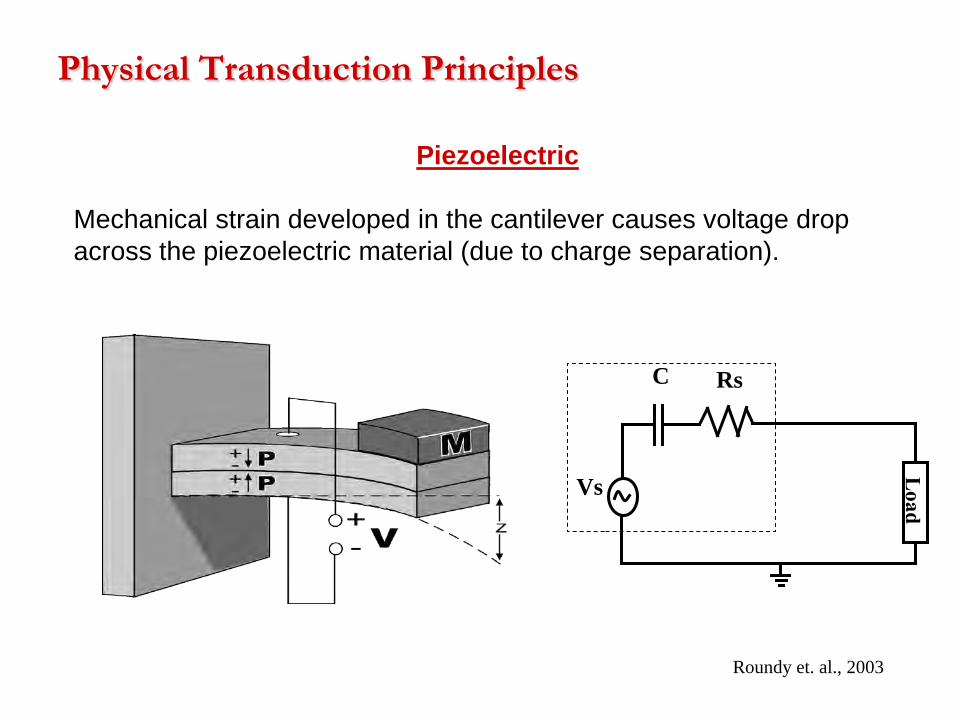
Physical Transduction Principles
Piezoelectric
Mechanical strain developed in the cantilever causes voltage drop across the piezoelectric material (due to charge separation).
Vs
C Rs
Roundy et. al., 2003
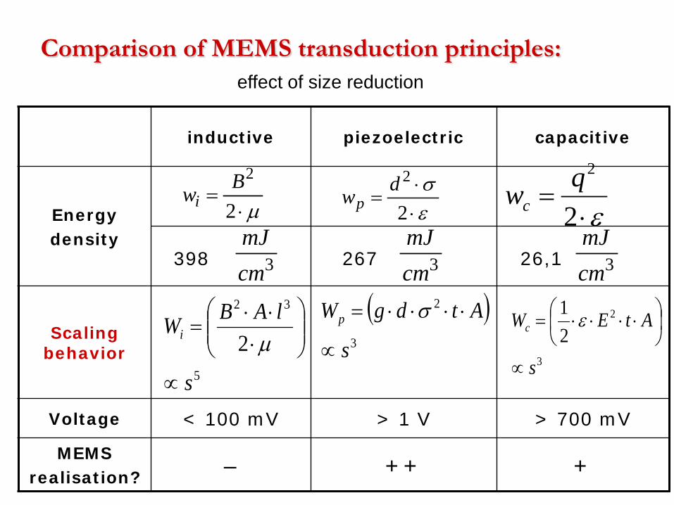
Comparison of MEMS transduction principles:
inductive piezoelectric capacitive
Energydensity
398 267 26,1
Scaling behavior
Voltage < 100 mV > 1 V > 700 mV
MEMSrealisation? – ++ +
µ⋅=
2
2Bwi εσ
⋅⋅
=2
2dwp ε⋅=
2
2qwc
3cmmJ
3cmmJ
3cmmJ
( )3
2
s
AtdgWp
∝
⋅⋅⋅⋅= σ
3
2
21
s
AtEWc
∝
⋅⋅⋅⋅= ε
5
32
2
s
lABWi
∝
⋅⋅⋅
=µ
effect of size reduction
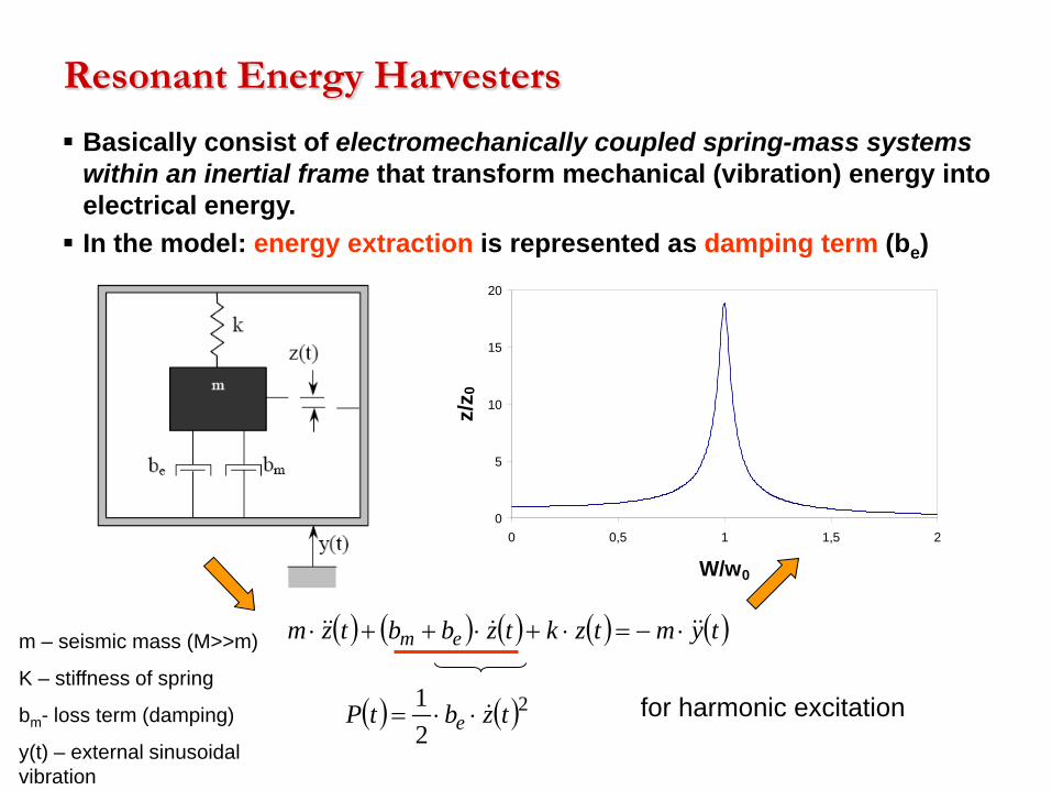
Resonant Energy Harvesters Basically consist of electromechanically coupled spring-mass systems
within an inertial frame that transform mechanical (vibration) energy into electrical energy. In the model: energy extraction is represented as damping term (be)
( ) ( ) ( ) ( ) ( )tymtzktzbbtzm em ⋅−=⋅+⋅++⋅
( ) ( )221 tzbtP e ⋅⋅=
0
5
10
15
20
0 0,5 1 1,5 2
W/w0
z/z 0
m – seismic mass (M>>m)
K – stiffness of spring
bm- loss term (damping)
y(t) – external sinusoidal vibration
for harmonic excitation
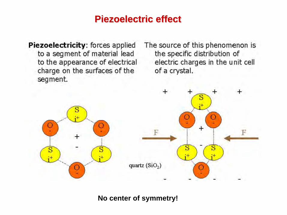
Piezoelectric effect
No center of symmetry!
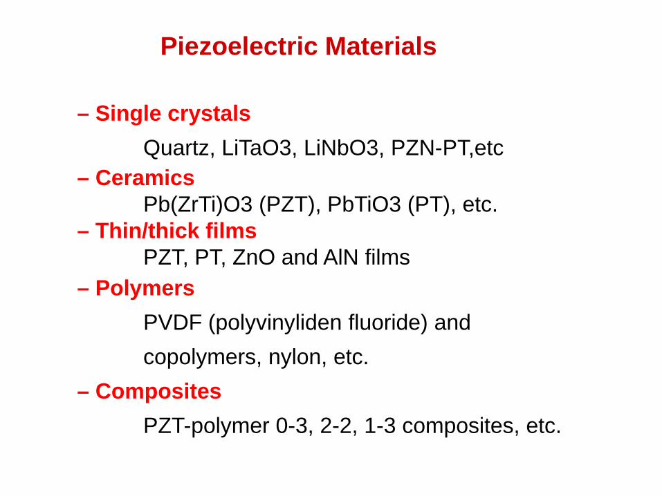
– Single crystalsQuartz, LiTaO3, LiNbO3, PZN-PT,etc
– CeramicsPb(ZrTi)O3 (PZT), PbTiO3 (PT), etc.
– Thin/thick filmsPZT, PT, ZnO and AlN films
– PolymersPVDF (polyvinyliden fluoride) and copolymers, nylon, etc.
– CompositesPZT-polymer 0-3, 2-2, 1-3 composites, etc.
Piezoelectric Materials
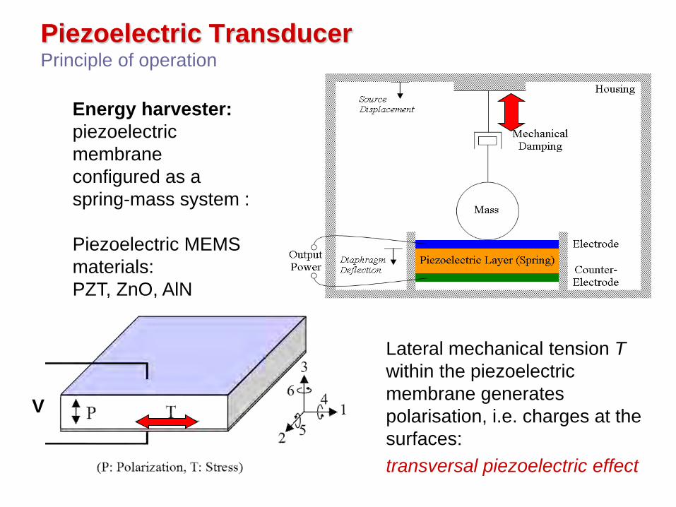
Piezoelectric TransducerPrinciple of operation
V
Energy harvester:piezoelectric membrane configured as a spring-mass system :
Piezoelectric MEMS materials: PZT, ZnO, AlN
Lateral mechanical tension Twithin the piezoelectric membrane generates polarisation, i.e. charges at the surfaces: transversal piezoelectric effect
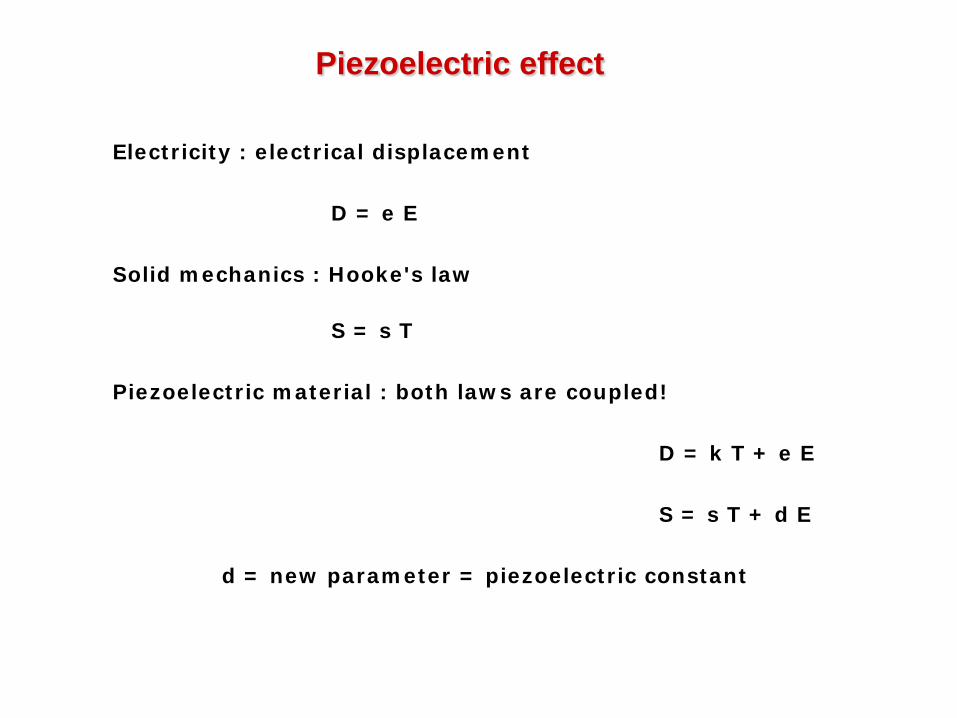
Piezoelectric effect
Electricity : electrical displacement
D = e E
Solid mechanics : Hooke's law
S = s T
Piezoelectric material : both laws are coupled!
D = k T + e E
S = s T + d E
d = new parameter = piezoelectric constant
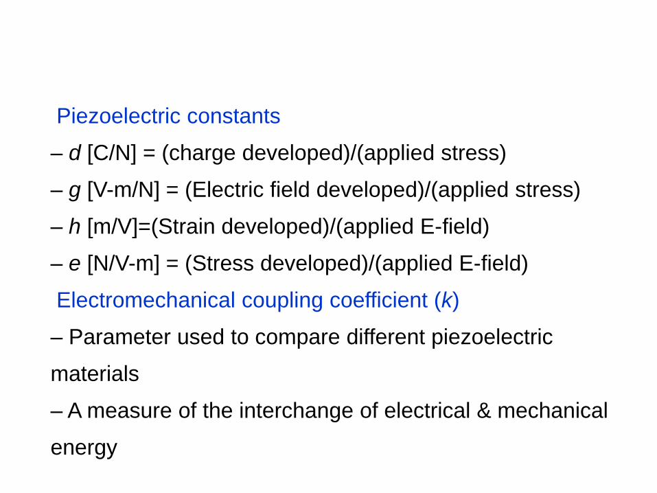
Piezoelectric constants
– d [C/N] = (charge developed)/(applied stress)
– g [V-m/N] = (Electric field developed)/(applied stress)
– h [m/V]=(Strain developed)/(applied E-field)
– e [N/V-m] = (Stress developed)/(applied E-field)
Electromechanical coupling coefficient (k)
– Parameter used to compare different piezoelectric
materials
– A measure of the interchange of electrical & mechanical
energy
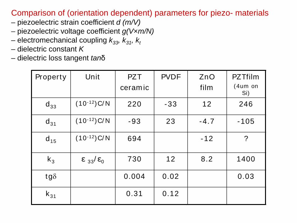
Property Unit PZTceramic
PVDF ZnOfilm
PZTfilm(4um on
Si)
d33 (10-12)C/N 220 -33 12 246
d31 (10-12)C/N -93 23 -4.7 -105
d15 (10-12)C/N 694 -12 ?
k3 ε 33/ε0 730 12 8.2 1400
tgδ 0.004 0.02 0.03
k31 0.31 0.12
Comparison of (orientation dependent) parameters for piezo- materials– piezoelectric strain coefficient d (m/V)– piezoelectric voltage coefficient g(V×m/N)– electromechanical coupling k33, k31, kt– dielectric constant K– dielectric loss tangent tanδ
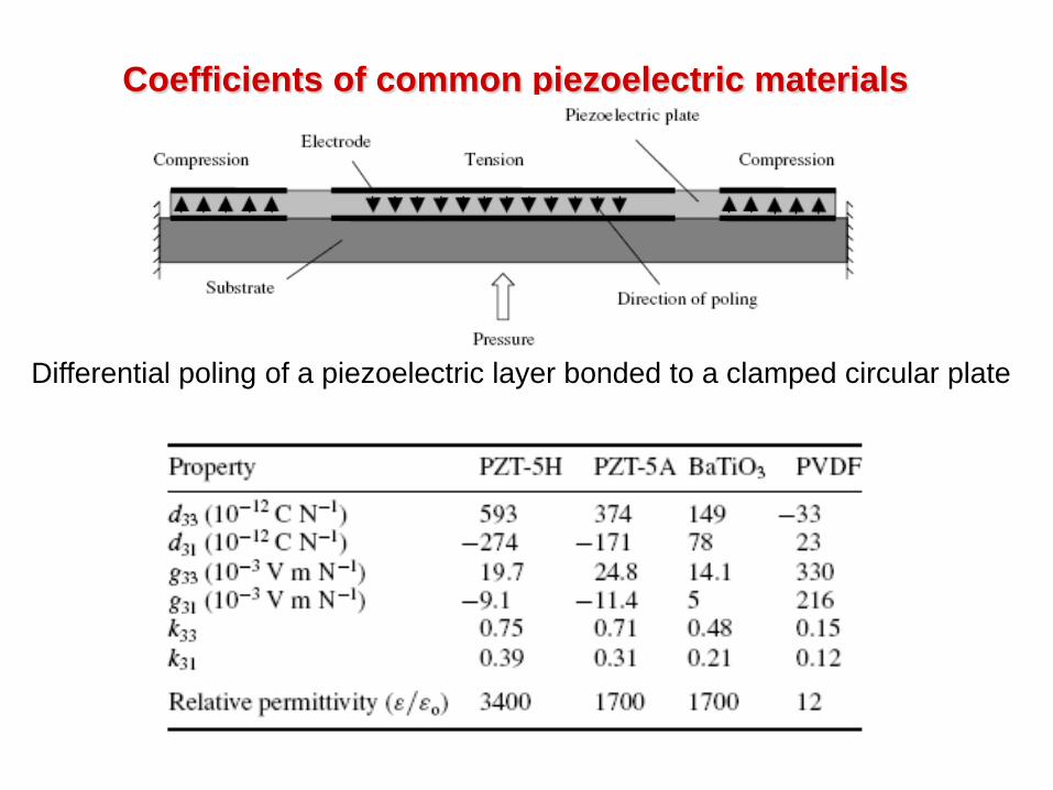
Coefficients of common piezoelectric materials
Differential poling of a piezoelectric layer bonded to a clamped circular plate
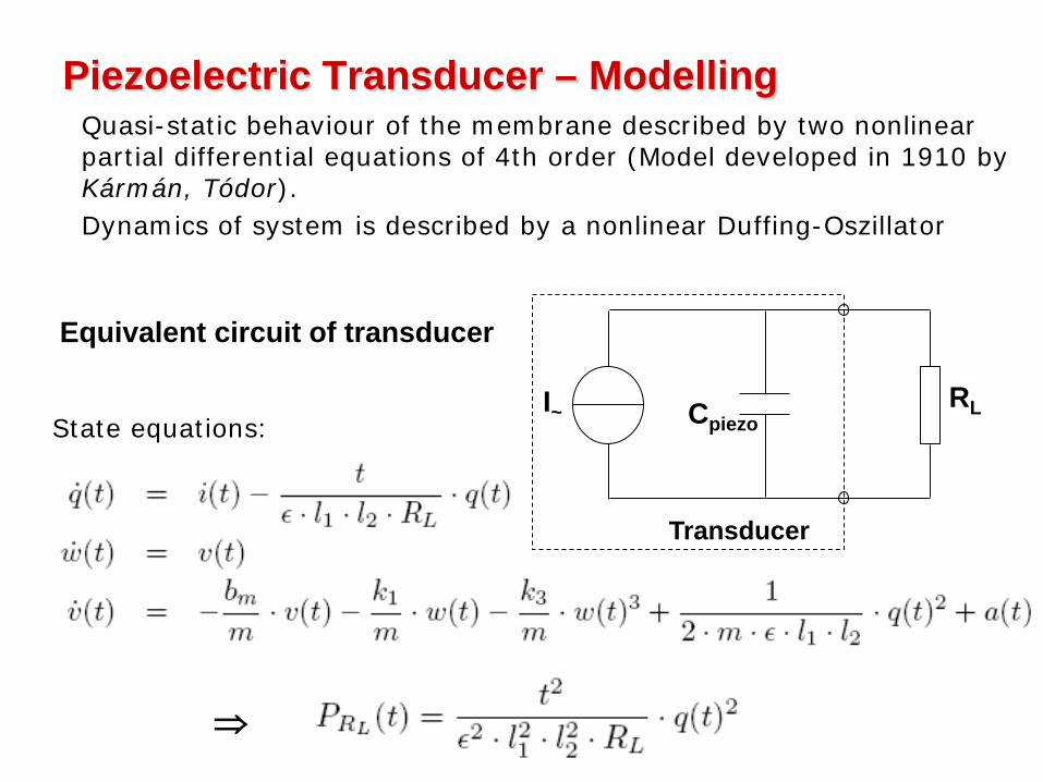
Piezoelectric Transducer – ModellingQuasi-static behaviour of the membrane described by two nonlinear partial differential equations of 4th order (Model developed in 1910 by Kármán, Tódor).Dynamics of system is described by a nonlinear Duffing-Oszillator
⇒
State equations: CpiezoRLI~
EnergiewandlerTransducer
Equivalent circuit of transducer
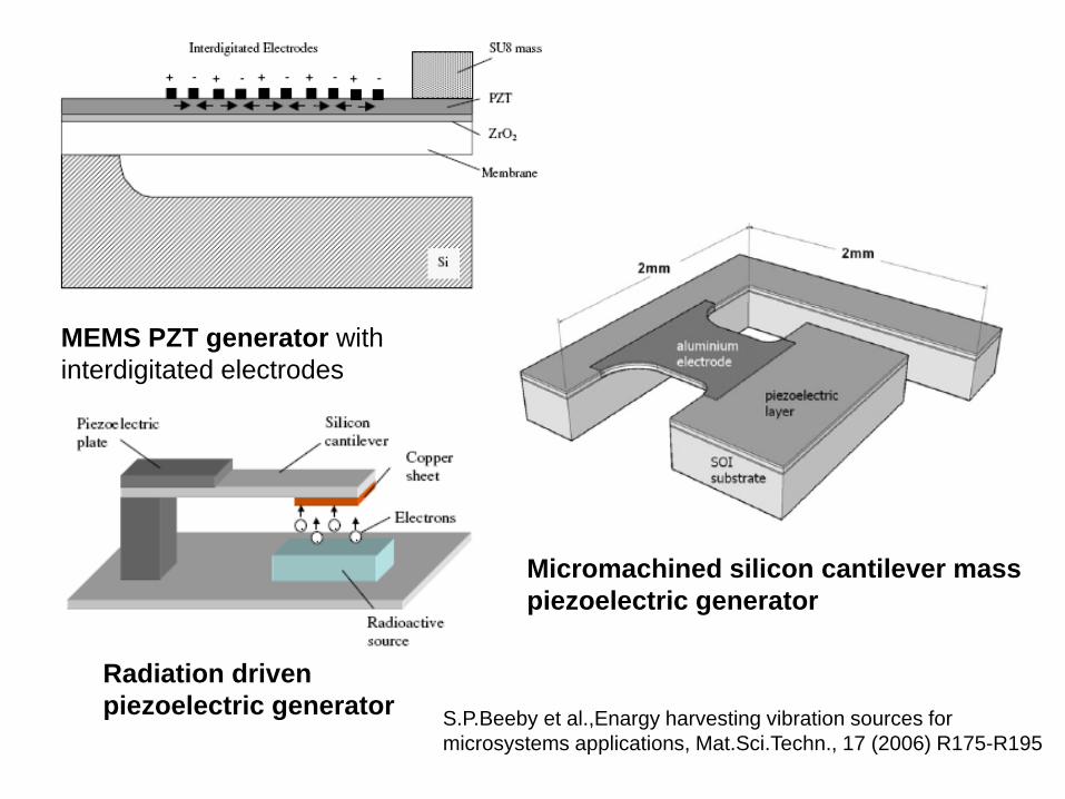
Radiation driven piezoelectric generator
MEMS PZT generator with interdigitated electrodes
Micromachined silicon cantilever mass piezoelectric generator
S.P.Beeby et al.,Enargy harvesting vibration sources for microsystems applications, Mat.Sci.Techn., 17 (2006) R175-R195
frequency ,Hz
Volta
ge o
utpu
t, m
V
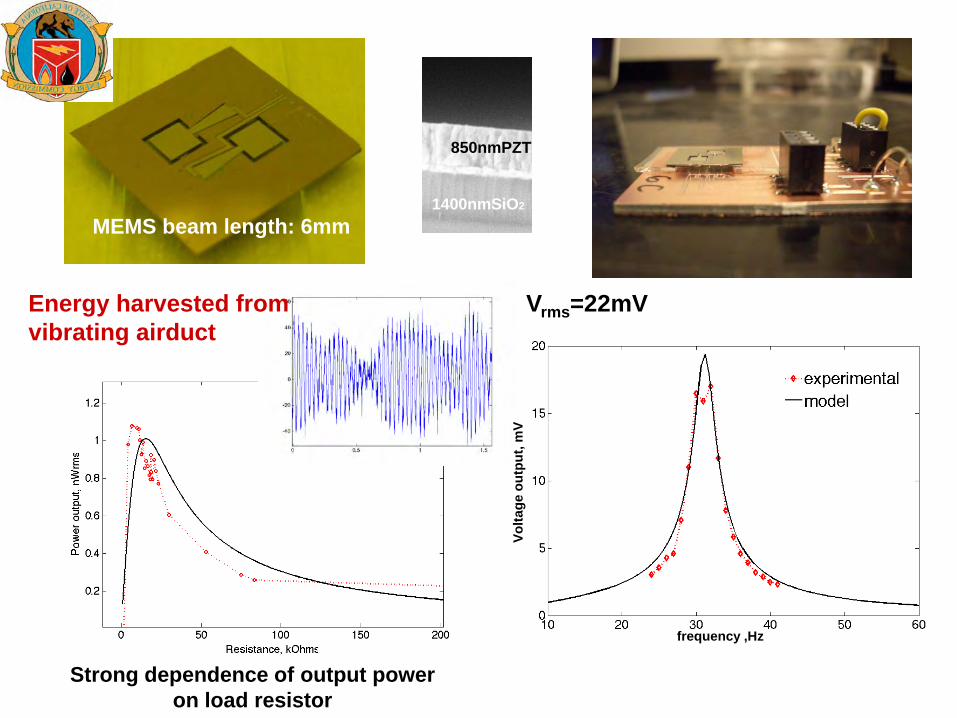
MEMS beam length: 6mm
850nmPZT
1400nmSiO2
Energy harvested from vibrating airduct
Vrms=22mV
Strong dependence of output power on load resistor
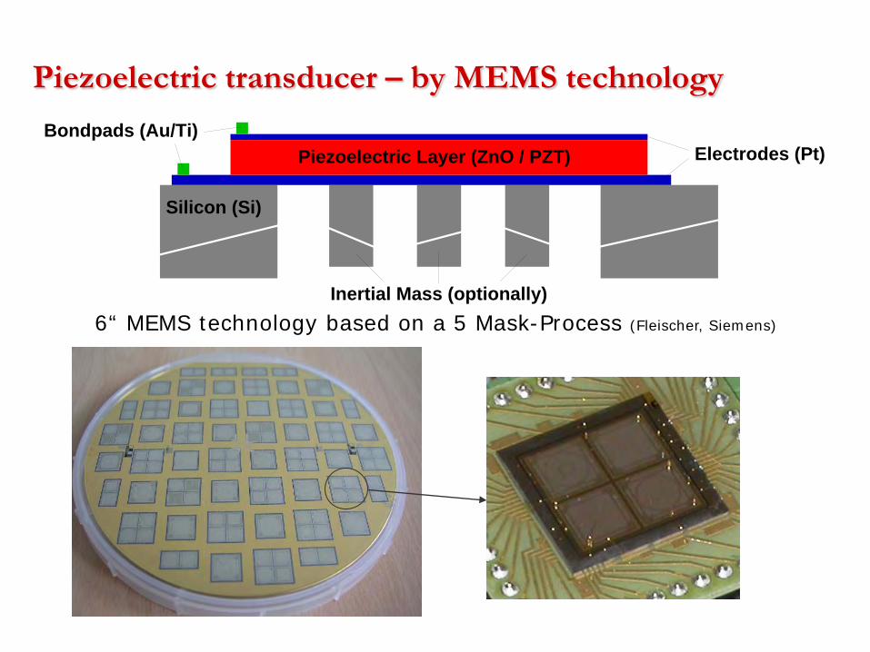
Piezoelectric transducer – by MEMS technology
Inertial Mass (optionally)
Electrodes (Pt)Piezoelectric Layer (ZnO / PZT)Bondpads (Au/Ti)
Silicon (Si)
6“ MEMS technology based on a 5 Mask-Process (Fleischer, Siemens)
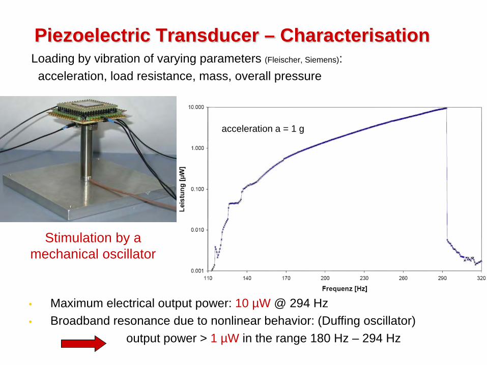
Piezoelectric Transducer – CharacterisationLoading by vibration of varying parameters (Fleischer, Siemens):
acceleration, load resistance, mass, overall pressure
Stimulation by a mechanical oscillator
acceleration a = 1 g
• Maximum electrical output power: 10 µW @ 294 Hz• Broadband resonance due to nonlinear behavior: (Duffing oscillator)
output power > 1 µW in the range 180 Hz – 294 Hz
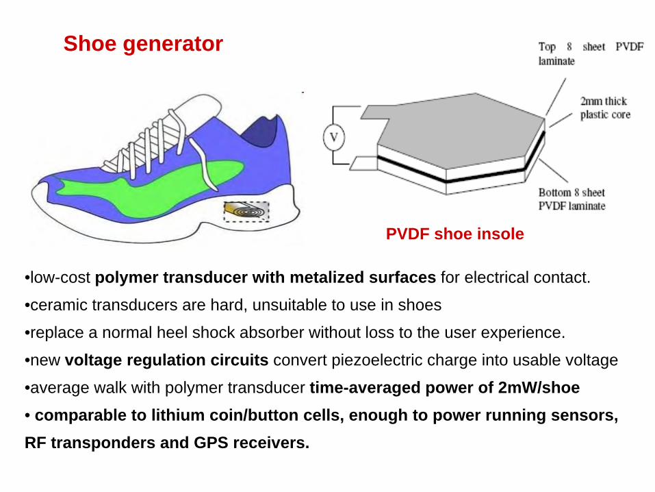
•low-cost polymer transducer with metalized surfaces for electrical contact.
•ceramic transducers are hard, unsuitable to use in shoes
•replace a normal heel shock absorber without loss to the user experience.
•new voltage regulation circuits convert piezoelectric charge into usable voltage
•average walk with polymer transducer time-averaged power of 2mW/shoe• comparable to lithium coin/button cells, enough to power running sensors, RF transponders and GPS receivers.
Shoe generator
PVDF shoe insole
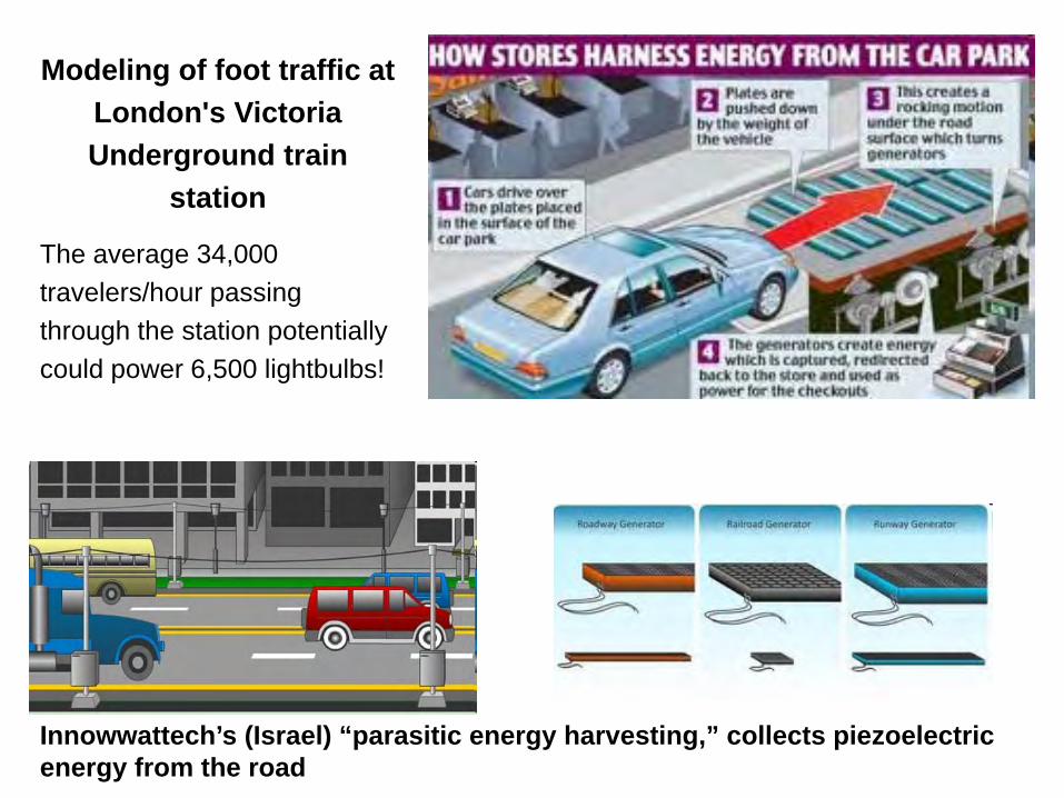
Modeling of foot traffic at London's Victoria Underground train
station
The average 34,000 travelers/hour passing through the station potentially could power 6,500 lightbulbs!
Innowwattech’s (Israel) “parasitic energy harvesting,” collects piezoelectric energy from the road
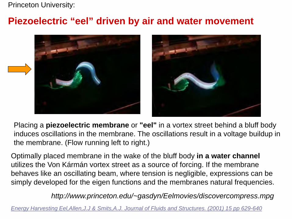
Placing a piezoelectric membrane or "eel" in a vortex street behind a bluff body induces oscillations in the membrane. The oscillations result in a voltage buildup in the membrane. (Flow running left to right.)
Princeton University:
Piezoelectric “eel” driven by air and water movement
http://www.princeton.edu/~gasdyn/Eelmovies/discovercompress.mpgEnergy Harvesting Eel,Allen,J.J & Smits,A.J. Journal of Fluids and Structures. (2001) 15 pp 629-640
Optimally placed membrane in the wake of the bluff body in a water channelutilizes the Von Kármán vortex street as a source of forcing. If the membrane behaves like an oscillating beam, where tension is negligible, expressions can be simply developed for the eigen functions and the membranes natural frequencies.
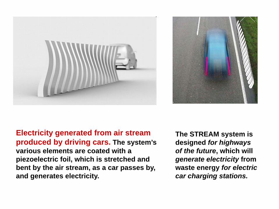
The STREAM system is designed for highways of the future, which will generate electricity from waste energy for electric car charging stations.
Electricity generated from air stream produced by driving cars. The system’s various elements are coated with a piezoelectric foil, which is stretched and bent by the air stream, as a car passes by, and generates electricity.
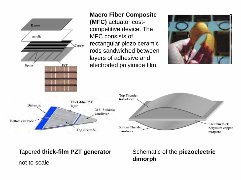
Macro Fiber Composite (MFC) actuator cost-competitive device. The MFC consists of rectangular piezo ceramic rods sandwiched between layers of adhesive and electroded polyimide film.
Tapered thick-film PZT generator
not to scale
Schematic of the piezoelectric dimorph
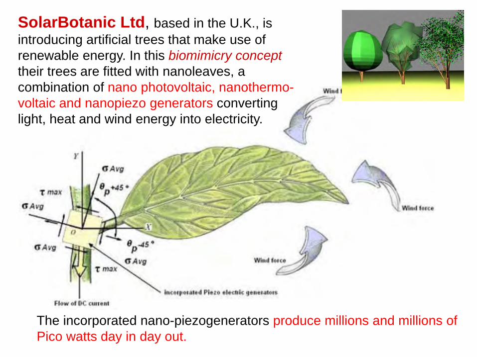
SolarBotanic Ltd, based in the U.K., is introducing artificial trees that make use of renewable energy. In this biomimicry concepttheir trees are fitted with nanoleaves, a combination of nano photovoltaic, nanothermo-voltaic and nanopiezo generators converting light, heat and wind energy into electricity.
The incorporated nano-piezogenerators produce millions and millions of Pico watts day in day out.
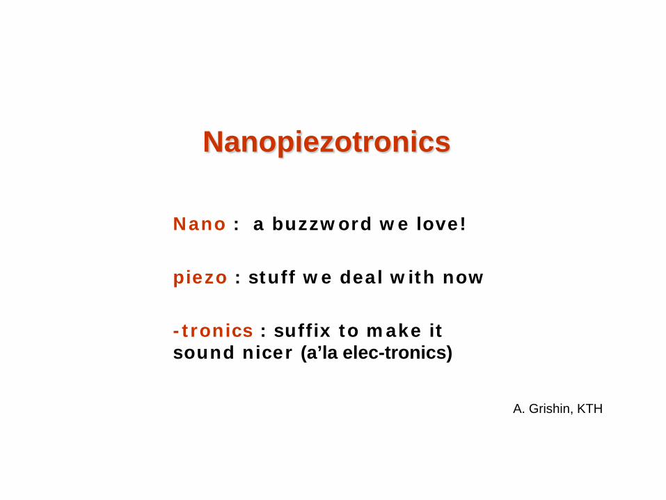
Nanopiezotronics
Nano : a buzzword we love!
piezo : stuff we deal with now
-tronics : suffix to make it sound nicer (a’la elec-tronics)
A. Grishin, KTH
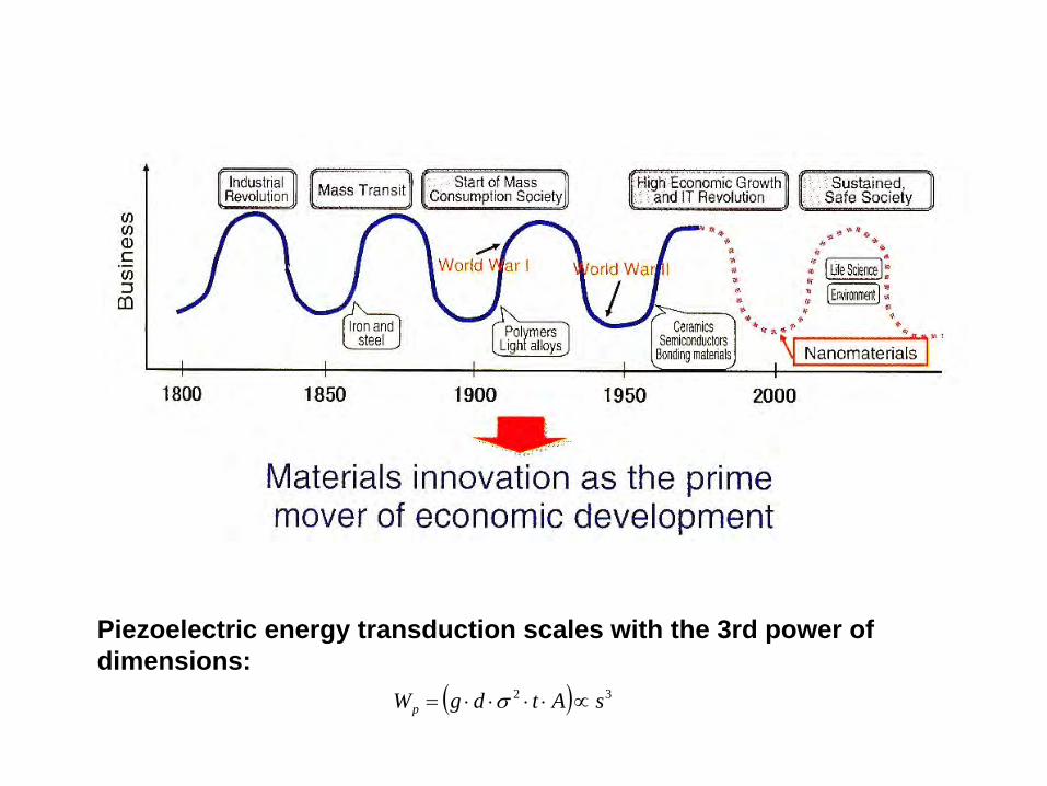
Piezoelectric energy transduction scales with the 3rd power of dimensions:
( ) 32 sAtdgWp ∝⋅⋅⋅⋅= σ
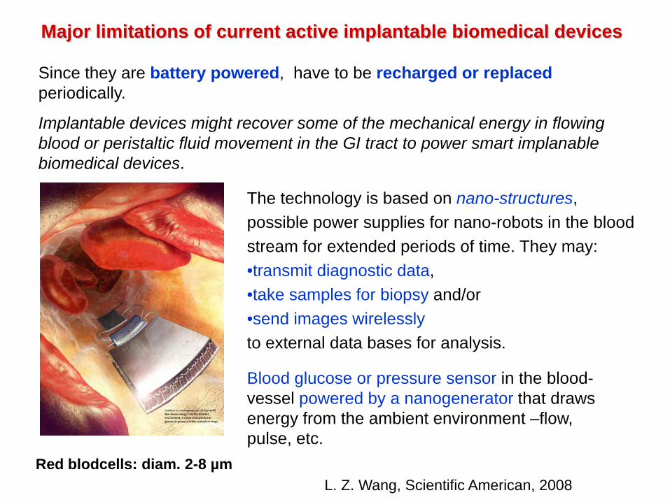
Since they are battery powered, have to be recharged or replacedperiodically.
Implantable devices might recover some of the mechanical energy in flowing blood or peristaltic fluid movement in the GI tract to power smart implanable biomedical devices.
The technology is based on nano-structures, possible power supplies for nano-robots in the blood stream for extended periods of time. They may: •transmit diagnostic data, •take samples for biopsy and/or •send images wirelesslyto external data bases for analysis.
Blood glucose or pressure sensor in the blood-vessel powered by a nanogenerator that draws energy from the ambient environment –flow, pulse, etc.
Major limitations of current active implantable biomedical devices
Red blodcells: diam. 2-8 µmL. Z. Wang, Scientific American, 2008
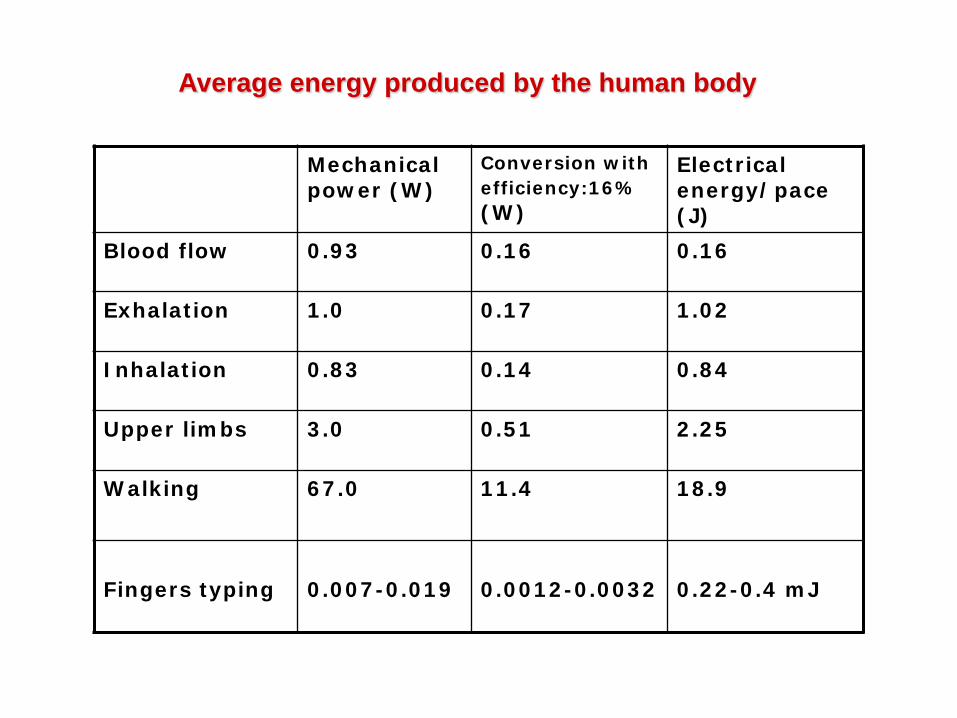
Mechanical power (W)
Conversion with efficiency:16%(W)
Electrical energy/pace (J)
Blood flow 0.93 0.16 0.16
Exhalation 1.0 0.17 1.02
Inhalation 0.83 0.14 0.84
Upper limbs 3.0 0.51 2.25
Walking 67.0 11.4 18.9
Fingers typing 0.007-0.019 0.0012-0.0032 0.22-0.4 mJ
Average energy produced by the human body
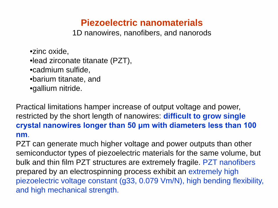
Piezoelectric nanomaterials1D nanowires, nanofibers, and nanorods
•zinc oxide, •lead zirconate titanate (PZT),•cadmium sulfide, •barium titanate, and •gallium nitride.
Practical limitations hamper increase of output voltage and power, restricted by the short length of nanowires: difficult to grow single crystal nanowires longer than 50 μm with diameters less than 100 nm.PZT can generate much higher voltage and power outputs than other semiconductor types of piezoelectric materials for the same volume, but bulk and thin film PZT structures are extremely fragile. PZT nanofibersprepared by an electrospinning process exhibit an extremely high piezoelectric voltage constant (g33, 0.079 Vm/N), high bending flexibility, and high mechanical strength.
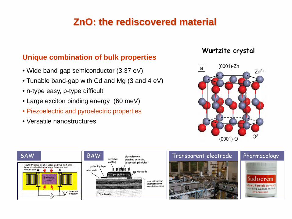
ZnO: the rediscovered material
Unique combination of bulk properties
• Wide band-gap semiconductor (3.37 eV) • Tunable band-gap with Cd and Mg (3 and 4 eV)• n-type easy, p-type difficult• Large exciton binding energy (60 meV)• Piezoelectric and pyroelectric properties• Versatile nanostructures
BAW Pharmacology
Wurtzite crystal
Transparent electrode SAW
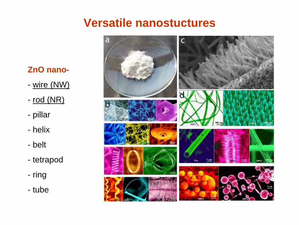
Versatile nanostuctures
ZnO nano-
- wire (NW)
- rod (NR)
- pillar
- helix
- belt
- tetrapod
- ring
- tube
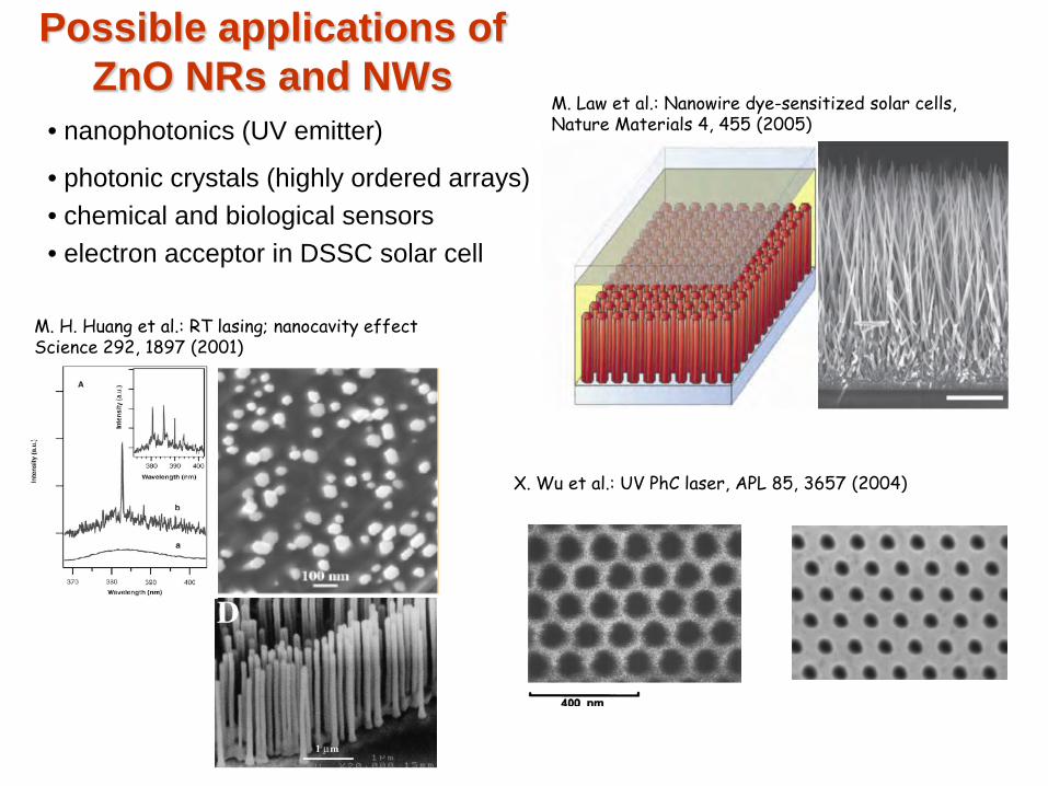
Possible applications of ZnO NRs and NWs
• nanophotonics (UV emitter)
• photonic crystals (highly ordered arrays)• chemical and biological sensors• electron acceptor in DSSC solar cell
M. Law et al.: Nanowire dye-sensitized solar cells,Nature Materials 4, 455 (2005)
M. H. Huang et al.: RT lasing; nanocavity effect Science 292, 1897 (2001)
X. Wu et al.: UV PhC laser, APL 85, 3657 (2004)
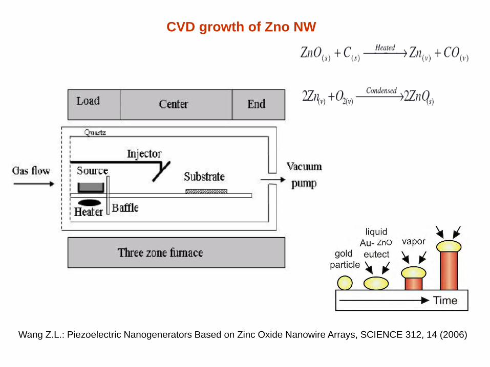
CVD growth of Zno NW
Wang Z.L.: Piezoelectric Nanogenerators Based on Zinc Oxide Nanowire Arrays, SCIENCE 312, 14 (2006)
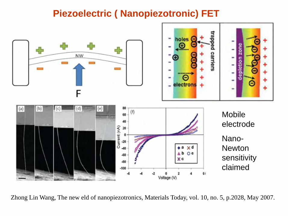
Piezoelectric ( Nanopiezotronic) FET
Zhong Lin Wang, The new eld of nanopiezotronics, Materials Today, vol. 10, no. 5, p.2028, May 2007.
Mobile electrode
Nano-Newton sensitivity claimed
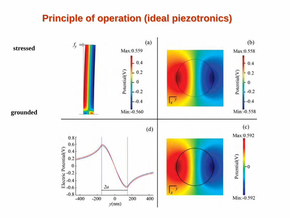
Principle of operation (ideal piezotronics)
grounded
stressed
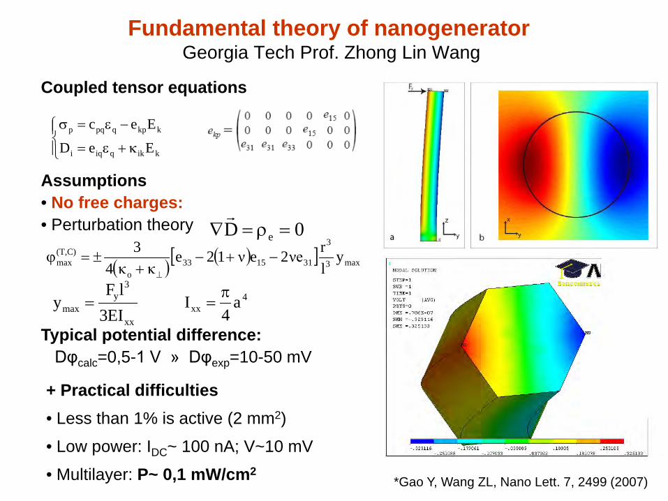
Fundamental theory of nanogeneratorGeorgia Tech Prof. Zhong Lin Wang
4
4rIkor
π=
( ) ( )[ ] max3
3
311533o
(T,C)max y
lrνe2eν12e
κκ43
−+−+
±=ϕ⊥
κ+ε=
−ε=σ
kikqiqi
kkpqpqp
EeD
Eec
*Gao Y, Wang ZL, Nano Lett. 7, 2499 (2007)
xx
3y
max EI3lF
y = 4xx a
4I π
=
Assumptions• No free charges:• Perturbation theory
Typical potential difference: Dφcalc=0,5-1 V » Dφexp=10-50 mV
0D e =ρ=∇
Coupled tensor equations
+ Practical difficulties• Less than 1% is active (2 mm2)
• Low power: IDC~ 100 nA; V~10 mV
• Multilayer: P~ 0,1 mW/cm2
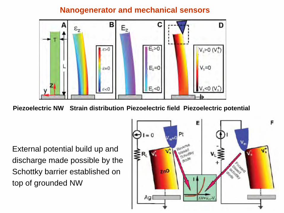
External potential build up and discharge made possible by the Schottky barrier established on top of grounded NW
Piezoelectric NW Strain distribution Piezoelectric field Piezoelectric potential
Nanogenerator and mechanical sensors
http://video.google.com/videoplay?docid=-1565105733906754975#
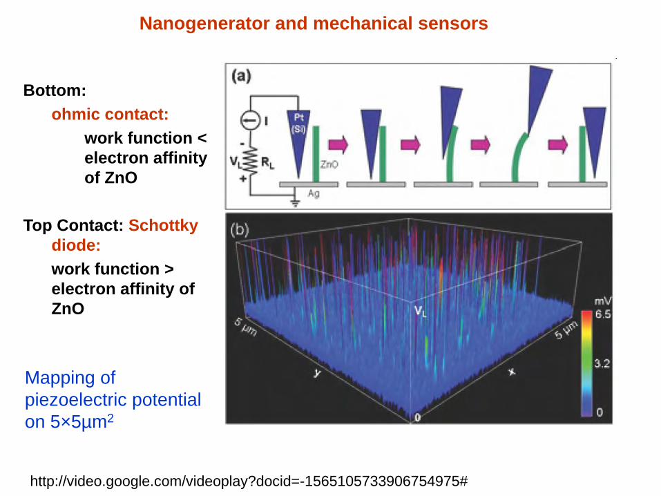
Nanogenerator and mechanical sensors
Bottom:ohmic contact:
work function < electron affinity of ZnO
Top Contact: Schottky diode:work function > electron affinity of ZnO
Mapping of piezoelectric potential on 5×5µm2
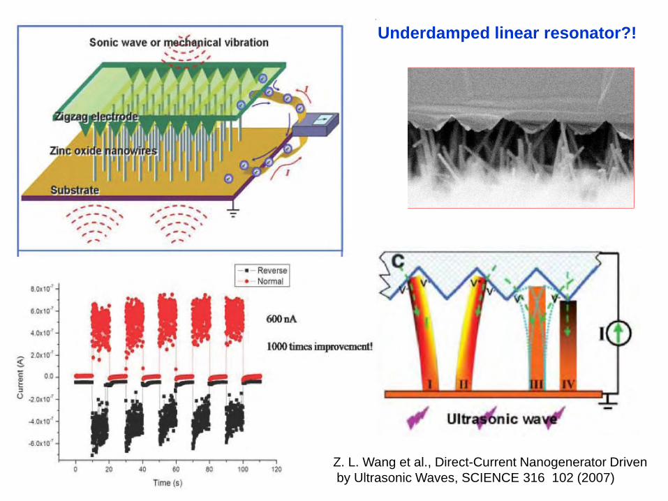
Z. L. Wang et al., Direct-Current Nanogenerator Drivenby Ultrasonic Waves, SCIENCE 316 102 (2007)
Underdamped linear resonator?!
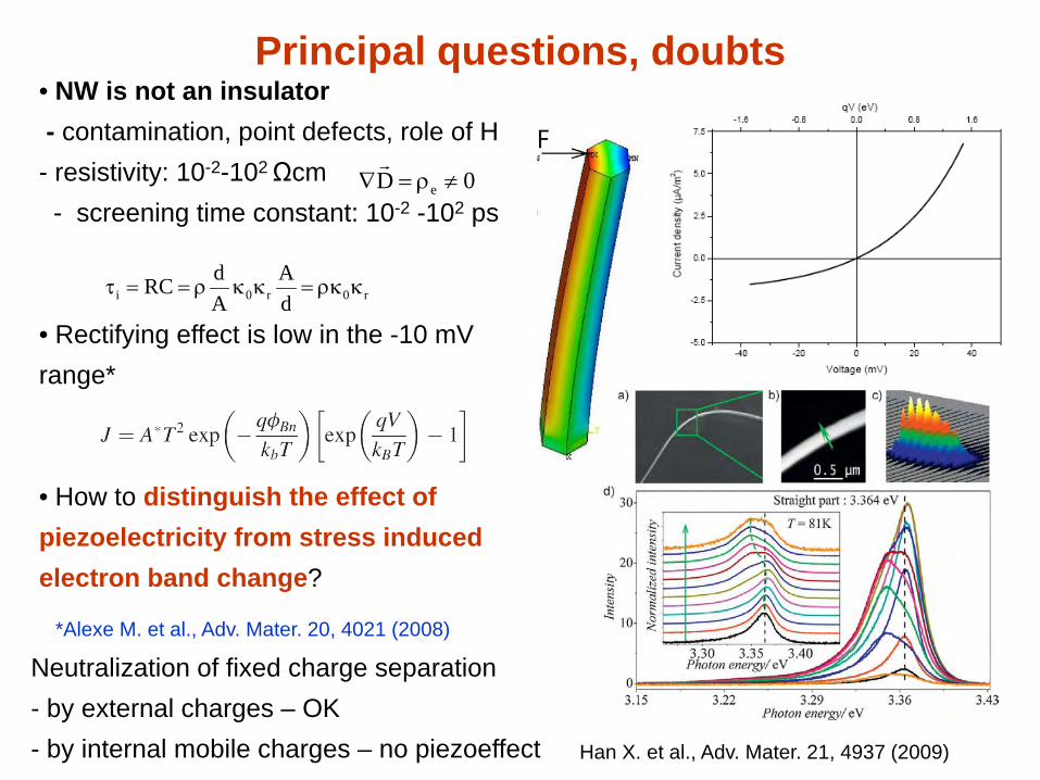
Principal questions, doubts
0D e ≠ρ=∇
• NW is not an insulator- contamination, point defects, role of H- resistivity: 10-2-102 Ωcm- screening time constant: 10-2 -102 ps
• Rectifying effect is low in the -10 mV range*
• How to distinguish the effect of piezoelectricity from stress induced electron band change?
r0r0i dA
AdRC κρκ=κκρ==τ
*Alexe M. et al., Adv. Mater. 20, 4021 (2008)
Han X. et al., Adv. Mater. 21, 4937 (2009)
Neutralization of fixed charge separation- by external charges – OK- by internal mobile charges – no piezoeffect
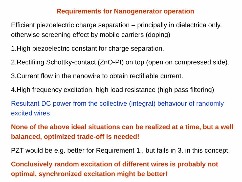
Requirements for Nanogenerator operation
Efficient piezoelectric charge separation – principally in dielectrica only, otherwise screening effect by mobile carriers (doping)
1.High piezoelectric constant for charge separation.
2.Rectifiing Schottky-contact (ZnO-Pt) on top (open on compressed side).
3.Current flow in the nanowire to obtain rectifiable current.
4.High frequency excitation, high load resistance (high pass filtering)
Resultant DC power from the collective (integral) behaviour of randomly excited wires
None of the above ideal situations can be realized at a time, but a well balanced, optimized trade-off is needed!
PZT would be e.g. better for Requirement 1., but fails in 3. in this concept.
Conclusively random excitation of different wires is probably not optimal, synchronized excitation might be better!
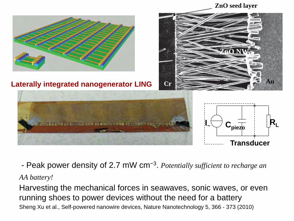
- Peak power density of 2.7 mW cm−3. Potentially sufficient to recharge an AA battery! Harvesting the mechanical forces in seawaves, sonic waves, or even running shoes to power devices without the need for a battery Sheng Xu et al., Self-powered nanowire devices, Nature Nanotechnology 5, 366 - 373 (2010)
Laterally integrated nanogenerator LING Cr Au
ZnO NW
CpiezoRLI~
EnergiewandlerTransducer
ZnO seed layer
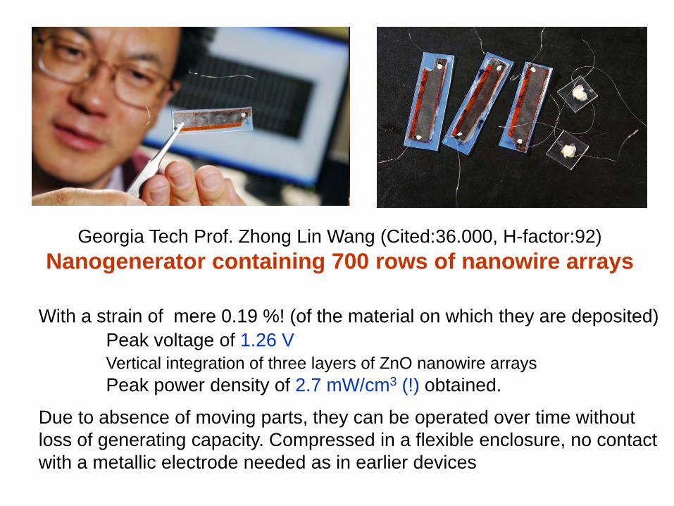
With a strain of mere 0.19 %! (of the material on which they are deposited)Peak voltage of 1.26 V Vertical integration of three layers of ZnO nanowire arraysPeak power density of 2.7 mW/cm3 (!) obtained.
Due to absence of moving parts, they can be operated over time without loss of generating capacity. Compressed in a flexible enclosure, no contact with a metallic electrode needed as in earlier devices
Georgia Tech Prof. Zhong Lin Wang (Cited:36.000, H-factor:92)Nanogenerator containing 700 rows of nanowire arrays
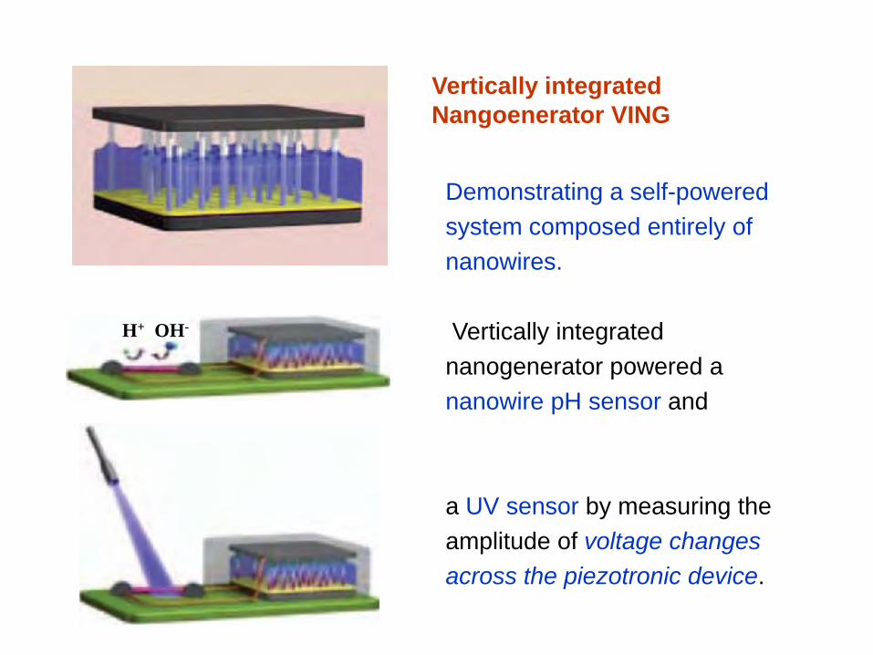
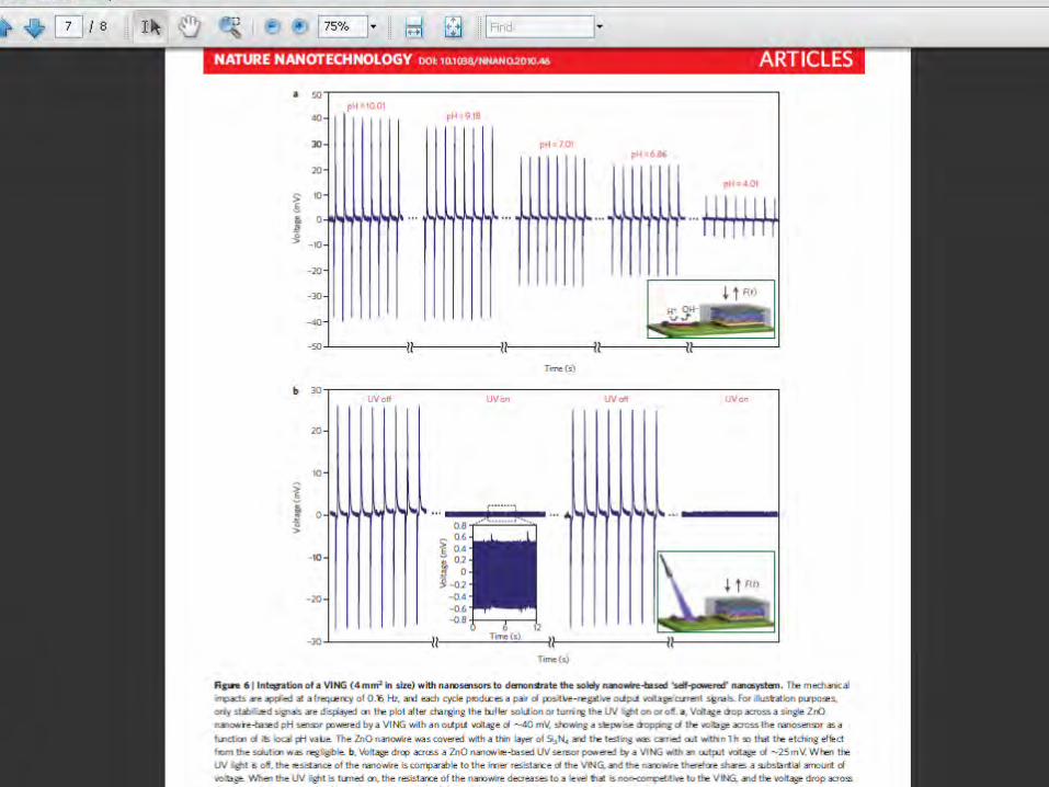
Vertically integrated Nangoenerator VING
Demonstrating a self-powered system composed entirely of nanowires.
Vertically integrated nanogenerator powered a nanowire pH sensor and
a UV sensor by measuring the amplitude of voltage changes across the piezotronic device.
H+ OH-
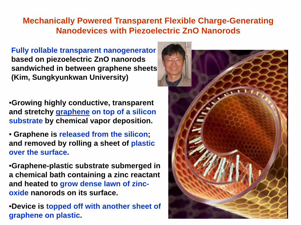
Fully rollable transparent nanogeneratorbased on piezoelectric ZnO nanorods sandwiched in between graphene sheets. (Kim, Sungkyunkwan University)
•Growing highly conductive, transparent and stretchy graphene on top of a silicon substrate by chemical vapor deposition.
• Graphene is released from the silicon; and removed by rolling a sheet of plastic over the surface.
•Graphene-plastic substrate submerged in a chemical bath containing a zinc reactant and heated to grow dense lawn of zinc-oxide nanorods on its surface.
•Device is topped off with another sheet of graphene on plastic.
Mechanically Powered Transparent Flexible Charge-Generating Nanodevices with Piezoelectric ZnO Nanorods
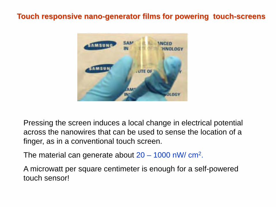
Pressing the screen induces a local change in electrical potential across the nanowires that can be used to sense the location of a finger, as in a conventional touch screen.
The material can generate about 20 – 1000 nW/ cm2.
A microwatt per square centimeter is enough for a self-powered touch sensor!
Touch responsive nano-generator films for powering touch-screens
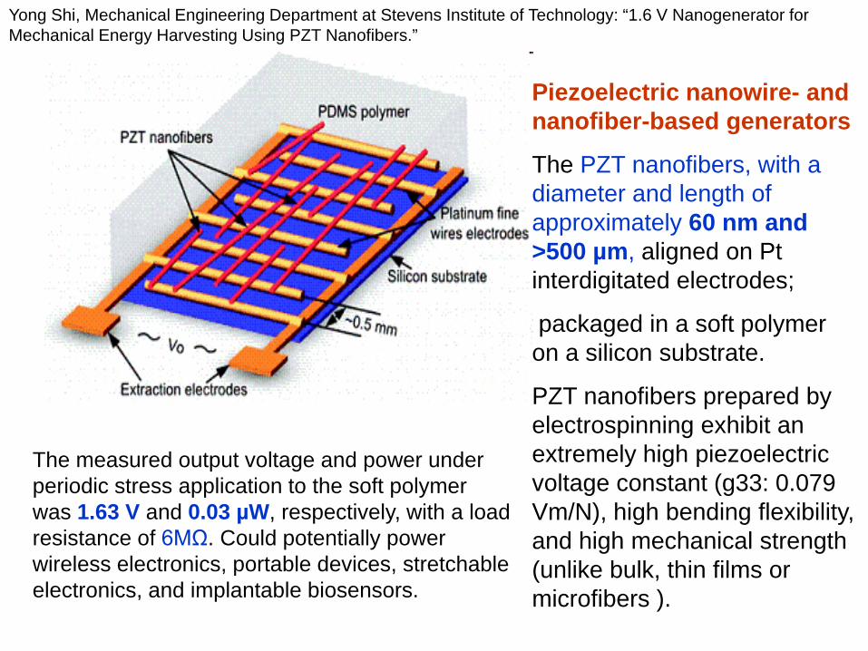
The measured output voltage and power under periodic stress application to the soft polymer was 1.63 V and 0.03 µW, respectively, with a load resistance of 6MΩ. Could potentially power wireless electronics, portable devices, stretchable electronics, and implantable biosensors.
Piezoelectric nanowire- and nanofiber-based generators
The PZT nanofibers, with a diameter and length of approximately 60 nm and >500 µm, aligned on Pt interdigitated electrodes;
packaged in a soft polymer on a silicon substrate.
PZT nanofibers prepared by electrospinning exhibit an extremely high piezoelectric voltage constant (g33: 0.079 Vm/N), high bending flexibility, and high mechanical strength (unlike bulk, thin films or microfibers ).
Yong Shi, Mechanical Engineering Department at Stevens Institute of Technology: “1.6 V Nanogenerator for Mechanical Energy Harvesting Using PZT Nanofibers.”
The PZT nanogenerator device fabrication• Electrospinning18 PZT nanofibers and depositing them on the preprepared interdigitated electrodes of platinum fine wire (diameter of 50 μm) arrays, which were assembled on a silicon substrate.
•Diameters of PZT nanofibers were controlled to be around 60 nm by varying the concentration of poly vinyl pyrrolidone (PVP) in the modified sol-gel solution.
•The PZT nanofibers obtained were continuous, while the distance between two adjacent electrodes was 500 μm as designed.
•A pure perovskite phase was obtained by annealing at 650 °C for about 25 min.
•Subsequently, a soft and polymer (polydimethylsiloxane, PDMS) was applied on top of the PZT nanofibers.
•The interdigitated electrodes of fine platinum wires were connected by extraction electrodes to transport harvested electrons to an external circuit.
•Finally, the PZT nanofibers were polled by applying an electric field of 4 V/ μm across the electrodes at a temperature of above 140 °C for about 24 h.
•The nanogenerator can be released from the silicon substrate or prepared on flexible substrates, depending on the requirements of the applications for energy harvesting.
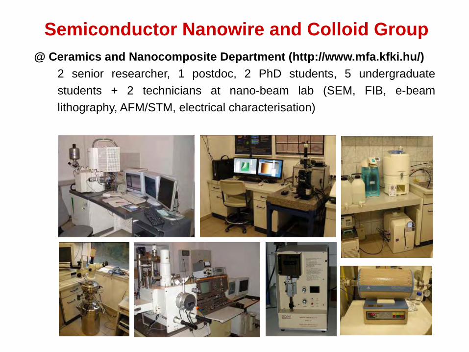
Semiconductor Nanowire and Colloid Group @ Ceramics and Nanocomposite Department (http://www.mfa.kfki.hu/)
2 senior researcher, 1 postdoc, 2 PhD students, 5 undergraduatestudents + 2 technicians at nano-beam lab (SEM, FIB, e-beamlithography, AFM/STM, electrical characterisation)
The MFA targets
1) Systematic investigation on well controlled NRs
• Electrical
• Mechanical
• Coupled electromechanical
2) Finding the origin of the „nanogenerator effect”
3) Fabrication of new type of mechanical sensor or energy converter
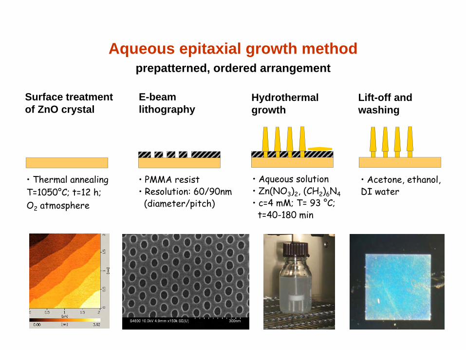
E-beam lithography
Surface treatment of ZnO crystal
Hydrothermal growth
• PMMA resist• Resolution: 60/90nm (diameter/pitch)
• Aqueous solution• Zn(NO3)2, (CH2)6N4• c=4 mM; T= 93 °C; t=40-180 min
Aqueous epitaxial growth methodprepatterned, ordered arrangement
Lift-off and washing
• Acetone, ethanol, DI water
• Thermal annealingT=1050°C; t=12 h; O2 atmosphere
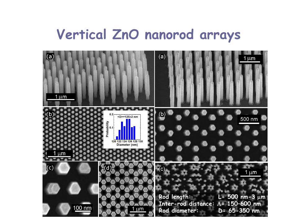
Vertical ZnO nanorod arrays
Rod length: L= 500 nm-3 µm Inter-rod distance: Λ= 150–600 nmRod diameter: D= 65-350 nm
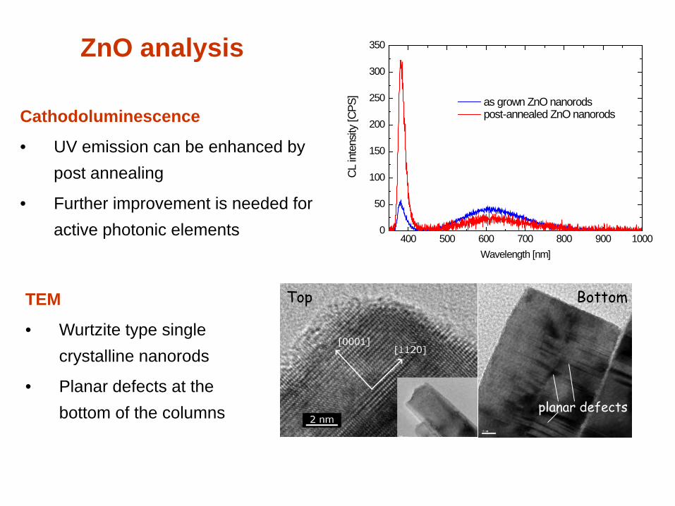
ZnO analysis
Cathodoluminescence
• UV emission can be enhanced by post annealing
• Further improvement is needed for active photonic elements
TEM
• Wurtzite type single crystalline nanorods
• Planar defects at the bottom of the columns
400 500 600 700 800 900 10000
50
100
150
200
250
300
350
as grown ZnO nanorods post-annealed ZnO nanorods
CL in
tens
ity [C
PS]
Wavelength [nm]
planar defects
BottomTop
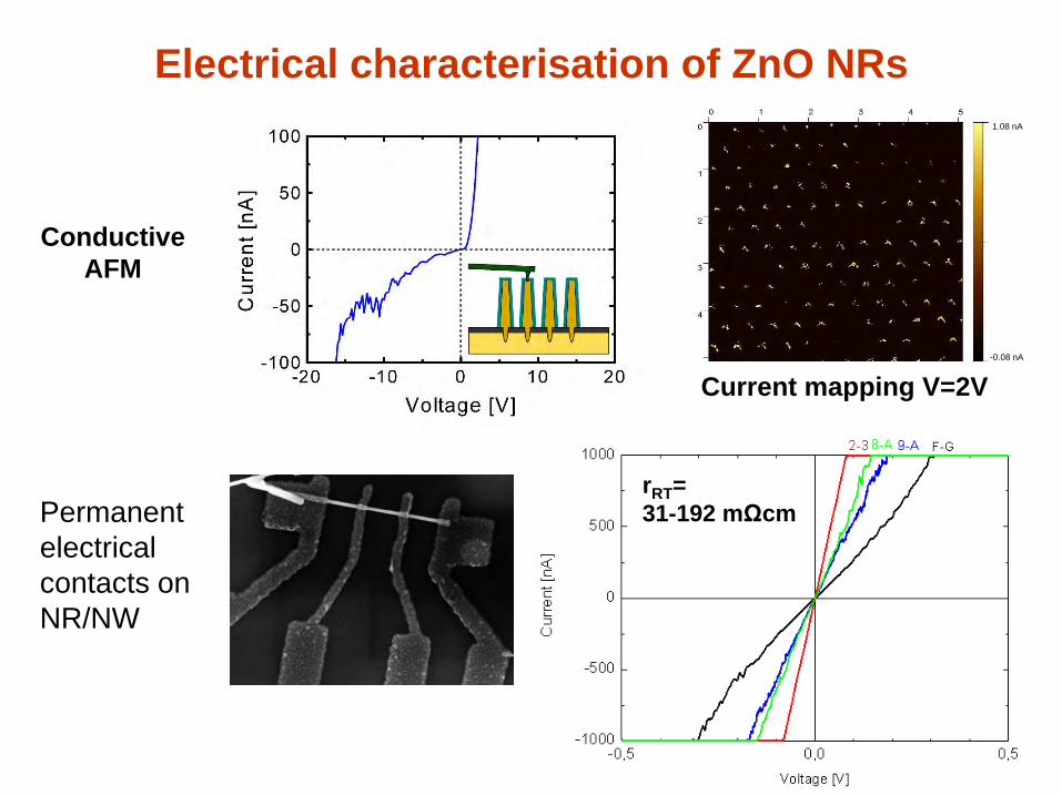
Electrical characterisation of ZnO NRs
rRT= 31-192 mΩcm
1.08 nA
-0.08 nA
SEMConductive AFM
Permanent electrical contacts on NR/NW
Current mapping V=2V
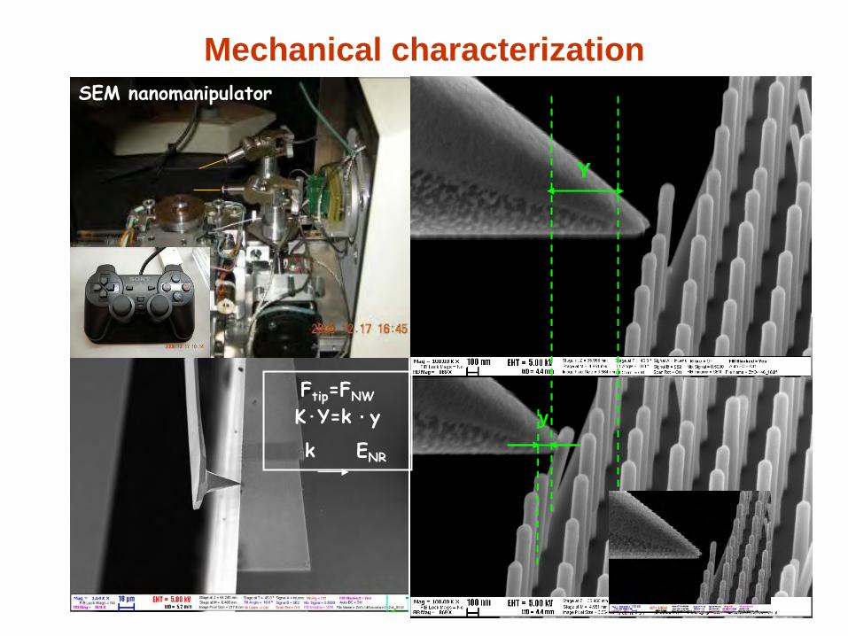
Mechanical characterizationSEM nanomanipulator
y
Y
Ftip=FNW
K∙Y=k · y
k ENR
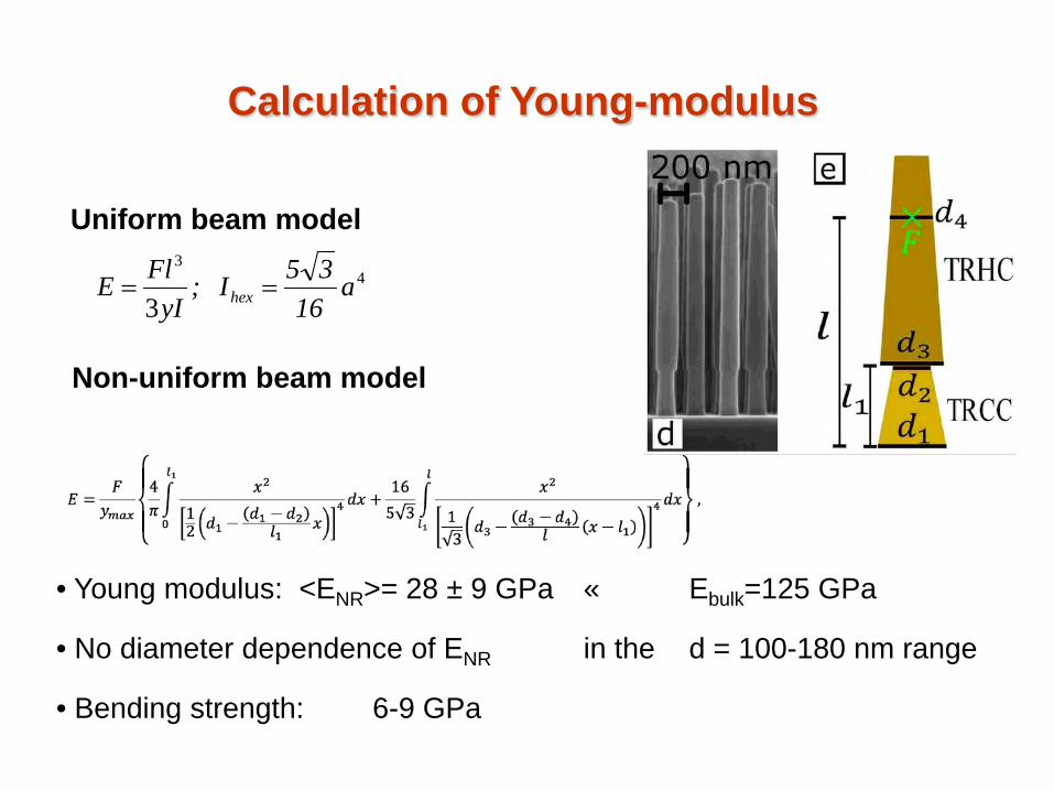
43
3a
1635I ;
yIFlE hex ==
• Young modulus: <ENR>= 28 ± 9 GPa « Ebulk=125 GPa
• No diameter dependence of ENR in the d = 100-180 nm range
• Bending strength: 6-9 GPa
Calculation of Young-modulus
Uniform beam model
Non-uniform beam model
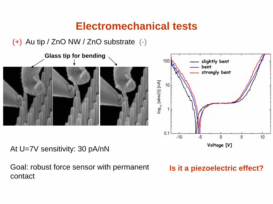
Electromechanical tests(+) Au tip / ZnO NW / ZnO substrate (-)
At U=7V sensitivity: 30 pA/nN
Goal: robust force sensor with permanent contact
Voltage [V]
slightly bentbentstrongly bent
Is it a piezoelectric effect?
Glass tip for bending
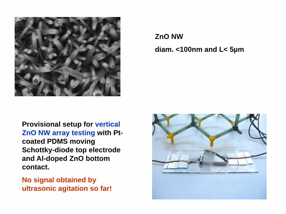
ZnO NW
diam. <100nm and L< 5µm
Provisional setup for vertical ZnO NW array testing with Pt-coated PDMS moving Schottky-diode top electrode and Al-doped ZnO bottom contact.
No signal obtained by ultrasonic agitation so far!
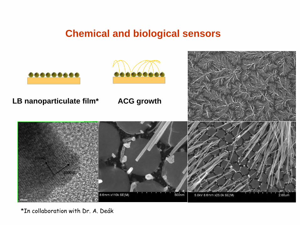
LB nanoparticulate film* ACG growth
Chemical and biological sensors
[0001]
_[1010]
*In collaboration with Dr. A. Deák
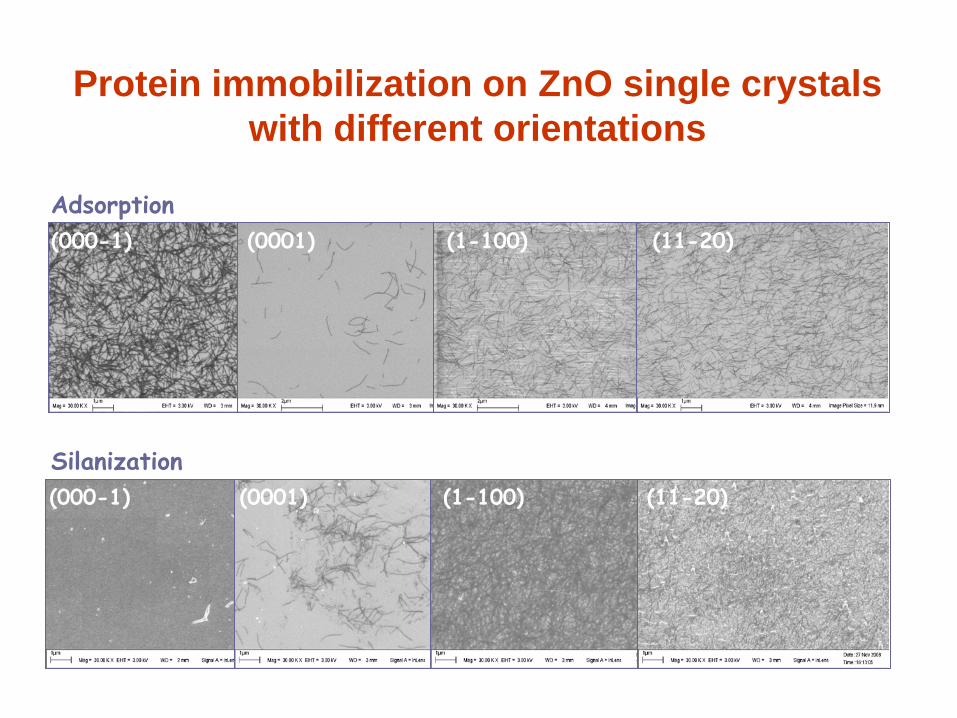
Adsorption
Silanization
Protein immobilization on ZnO single crystals with different orientations
(000-1)
(000-1)
(0001)
(0001)
(1-100)
(1-100)
(11-20)
(11-20)
Summary
Due to scaling, piezoelectric nanostructures seem to be
feasible for constructing energy scavenging nanodevices.
Parallel connection of the nanowires may reduce the operation
frequency but also the conversion efficiency
Adventage expected there, where multipurpose applications
are possible:
the stressing of wires produces the power for detection
of some parameters with the same nanowires: e.g. of
pH, stress, some chemical or biosubstance, etc.

Thanks for your attention!

Provocative question
If the ideal efficiency can not be increased in case of physical
systems, only in chemical (e.g. fuel cells) or biological
processes (APT,ADP-P) - optimised by evolution throughout
millions of years-, what is the point in minimizing –
irreproducibly -physical dimensions without limits?
Don’t we have to go rather for mimicing energy efficient bio-
systems?