Embed Size (px)
Citation preview
€ 3 3 0
0 W
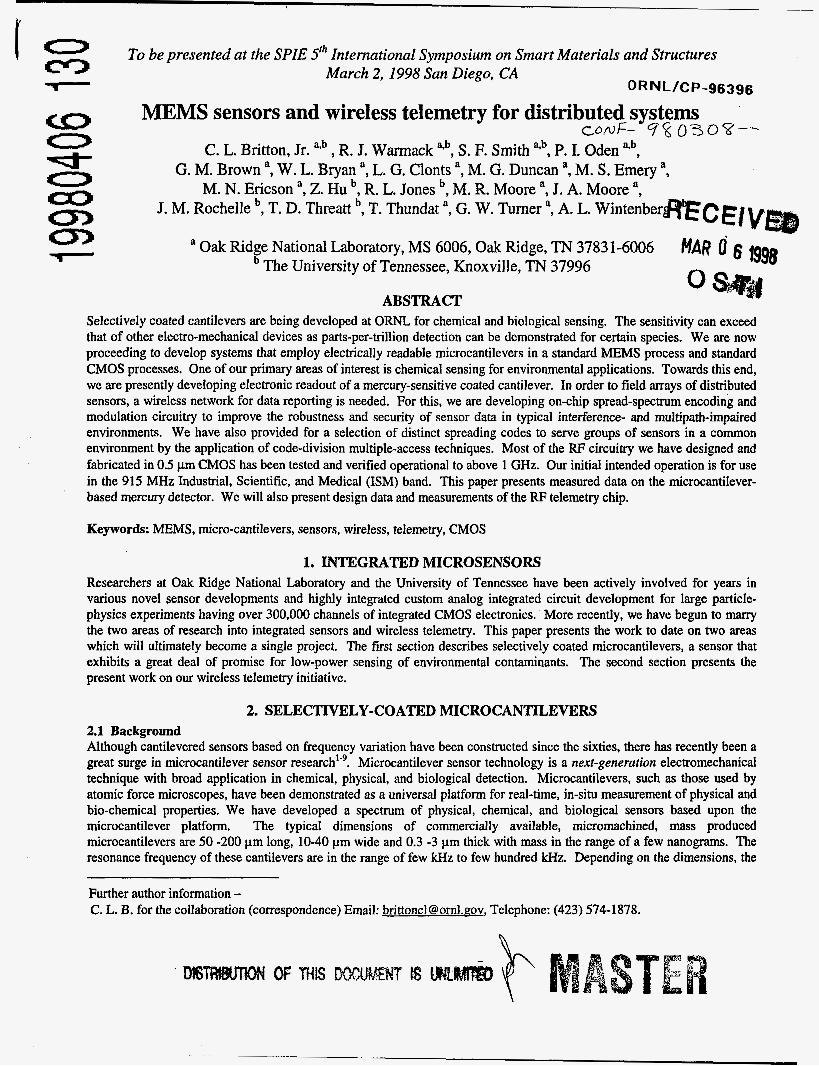
To be presented at the SPIE 5'h International Symposium on Smart Materials and Structures March 2, I998 San Diego, CA
oRNL/CP-96396
MEMS sensors and wireless telemetry for distributed systems C O # F - 9% 0 3 3 8 - - - -
C. L. Britton, Jr. , R. J. Warmack 'by S . F. Smith 'b, P. I. Oden ab,
M. N. Ericson ', Z. Hu R. L. Jones b, M. R. Moore ', J. A. Moore ', G. M. Brown ', W. L. Bryan ', L. G. Clonts ', M. G. Duncan ', M. S. Emery ',
J. M. Rochelle b, T. D. Threatt T. Thundat ', G. W. Turner ', A. L. W i n t e n b e r R E C €1 v a Oak Ridge National Laboratory, MS 6006, Oak Ridge, TN 3783 1-6006
The University of Tennessee, Knoxville, TN 37996
ABSTRACT
MAR 6 1398 0
Selectively coated cantilevers are being developed at ORNL, for chemical and biological sensing. The sensitivity can exceed that of other electro-mechanical devices as parts-per-trillion detection can be demonstrated for certain species. We are now proceeding to develop systems that employ electrically readable microcantilevers in a standard MEMS process and standard CMOS processes. One of our primary areas of interest is chemical sensing for environmental applications. Towards this end, we are presently developing electronic readout of a mercury-sensitive coated cantilever. In order to field arrays of distributed sensors, a wireless network for data reporting is needed. For this, we are developing on-chip spread-spectrum encoding and modulation circuitry to improve the robustness and security of sensor data in typical interference- and multipath-impaired environments. We have also provided for a selection of distinct spreading codes to serve groups of sensors in a common environment by the application of code-division multiple-access techniques. Most of the RF circuitry we have designed and fabricated in 0.5 pm CMOS has been tested and verified operational to above 1 GHz. Our initial intended operation is for use in the 915 MHz Industrial, Scientific, and Medical (ISM) band. This paper presents measured data on the microcantilever- based mercury detector. We will also present design data and measurements of the RF telemetry chip.
Keywords: MEMS, micro-cantilevers, sensors, wireless, telemetry, CMOS
1. INTEGRATED MICROSENSORS Researchers at Oak Ridge National Laboratory and the University of Tennessee have been actively involved for years in various novel sensor developments and highly integrated custom analog integrated circuit development for large particle- physics experiments having over 300,000 channels of integrated CMOS electronics. More recently, we have begun to marry the two areas of research into integrated sensors and wireless telemetry. This paper presents the work to date on two areas which will ultimately become a single project. The first section describes selectively coated microcantilevers, a sensor that exhibits a great deal of promise for low-power sensing of environmental contaminants. The second section presents the present work on our wireless telemetry initiative.
2. SELECTIVELY-COATED MICROCANTILEVERS 2.1 Background Although cantilevered sensors based on frequency variation have been constructed since the sixties, there has recently been a great surge in microcantilever sensor research'-'. Microcantilever sensor technology is a next-generation electromechanical technique with broad application in chemical, physical, and biological detection. Microcantilevers, such as those used by atomic force microscopes, have been demonstrated as a universal platform for real-time, in-situ measurement of physical and bio-chemical properties. We have developed a spectrum of physical, chemical, and biological sensors based upon the microcantilever platform. The typical dimensions of commercially available, micromachined, mass produced microcantilevers are 50 -200 pm long, 10-40 pm wide and 0.3 -3 pm thick with mass in the range of a few nanograms. The resonance frequency of these cantilevers are in the range of few kHz to few hundred kHz. Depending on the dimensions, the
Further author information - C. L. B. for the collaboration (correspondence) Email: [email protected], Telephone: (423) 574-1878.
DISCLAIMER
This report was prepared as an account of work sponsored by an agency of the United States Government. Neither the United States Government nor any agency thereof, nor any of their employees, makes any warranty, express or implied. or assumes any legal liability or responsibility for the accuracy, completeness, or use- fulness of any information, apparatus, product, or process disclosed, or represents that its use would not infringe privately owned rights. Reference herein to any spe- cific commercial product, process, or service by trade name, trademark, manufac- turer, or otherwise does not necessarily constitute or imply its endorsement, recom- mendation, or favoring by the United States Government or any agency thereof. The views and opinions of authors expressed herein do not necessarily state or reflect those of the United States Government or any agency thereof.
To be presented at the SPIE 5th International Symposium on Smart Materials and Structures March 2,1998 San Diego, CA 1
cantilcver spring constant can vary from 0.008 - 30 N/m. The deflections of these cantilevers can be detected with sub- Angstrom precision using current techniques perfected for AFM technology such as optical, piezoresistive, piezoelectric, capacitive, and electron tunneling". Sensitive detection of the cantilever deflection due to adsorption-induced forces and resonance frequency variation due to mass loading can result in part-per-billion (ppb) to part-per-trillion (ppt) sensitivity". Chemical selectivity can be achieved by using chemically selective coatings on the cantilevers. We have demonstrated a number of extremely sensitive physical, chemical, and biological sensors using microcantilevers. Examples include relative humidity, mercury vapor, mercaptans, toluene, viscosity, infrared and ultraviolet flow rate, lead in water", DNA hybridization, and antibody-antigen interaction.
Until recently, we used only commercially available, V-shaped silicon nitride and silicon cantilevers with a typical dimension of 100-200 pm length, 20-40 pm width and 0.6 pm thickness in these experiments (available from Digital Instruments, CA, and Parks scientific, CA). The cantilevers were first degreased and stripped of gold. A fresh 40 nm layer of gold was later evaporated on one side of the cantilever. The cantilevers were set into vibration by a piezoelectric cantilever holder driven by an external ac voltage. For detecting relative humidity, a thin layer of gelatin was deposited on the cantilever. Readout of the position of the cantilever tip was performed by reflecting a laser off the tip to an optical detector. This allows excellent sensitivity but requires alignment of the optical path, is limited to one (or at least very few) cantilever at a time, and requires a great deal of power.
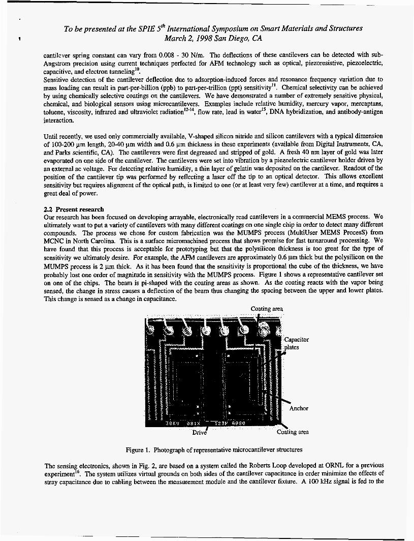
2.2 Present research Our research has been focused on developing arrayable, electronically read cantilevers in a commercial MEMS process. We ultimately want to put a variety of cantilevers with many different coatings on one single chip in order to detect many different compounds. The process we chose for custom fabrication was the MUMPS process (Multiuser MEMS Process) from MCNC in North Carolina. This is a surface micromachined process that shows promise for fast turnaround processing. We have found that this process is acceptable for prototyping but that the polysilicon thickness is too great for the type of sensitivity we ultimately desire. For example, the AFM cantilevers are approximately 0.6 pm thick but the polysilicon on the MUMPS process is 2 pm thick. As it has been found that the sensitivity is proportional the cube of the thickness, we have probably lost one order of magnitude in sensitivity with the MUMPS process. Figure 1 shows a representative cantilever set on one of the chips. The beam is pi-shaped with the coating areas as shown. As the coating reacts with the vapor being sensed, the change in stress causes a deflection of the beam thus changing the spacing between the upper and lower plates. This change is sensed as a change in capacitance.
Coating area
Capacitor plates
I Drive
\ Anchor
\ Coating area
Figure 1. Photograph of representative microcantilever structures
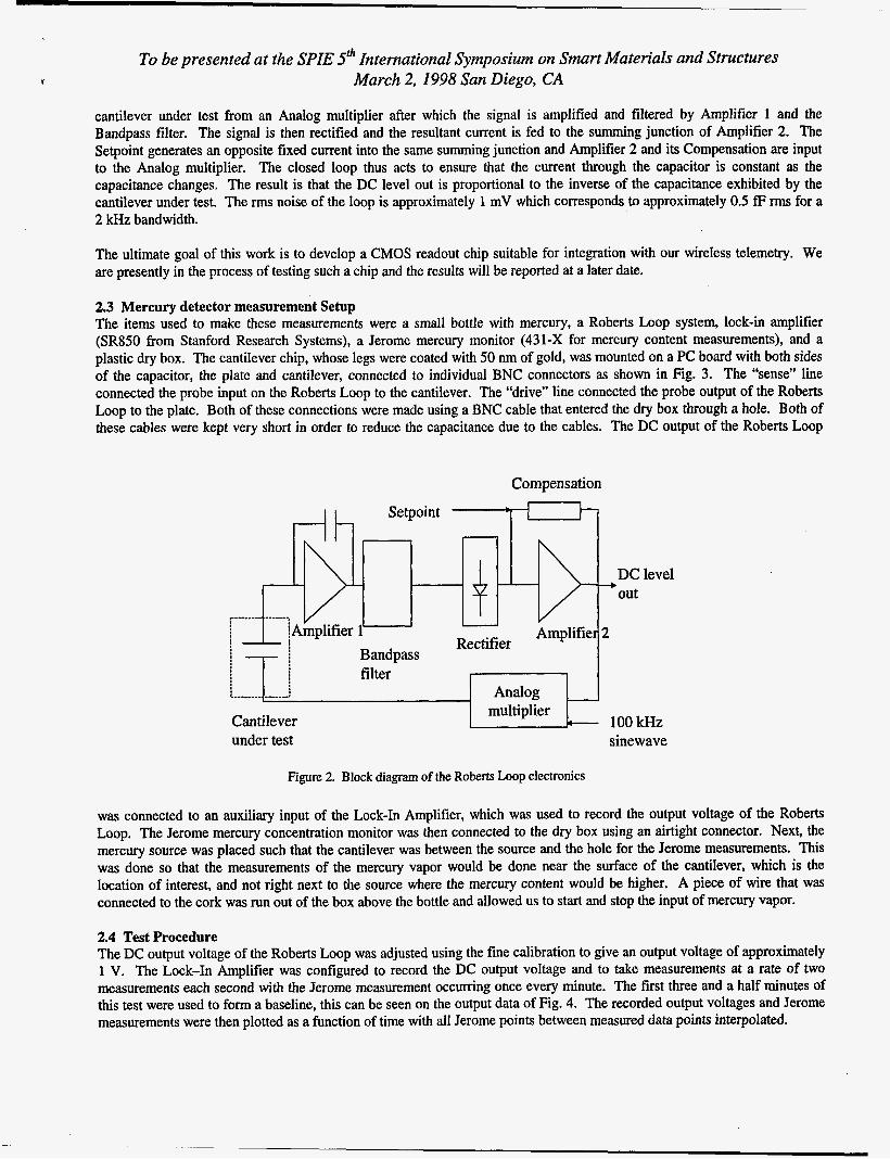
The sensing electronics, shown in Fig. 2, are based on a system called the Roberts Loop developed at ORNL, for a previous experiment16. The system utilizes virtual grounds on both sides of the cantilever capacitance in order minimize the effects of stray capacitance due to cabling between the measurement module and the cantilever fixture. A 100 kHz signal is fed to the
Y
To be presented at the SPIE Jth International Symposium on Smart Materials and Structures March 2,1998 San Diego, CA
cantilever under test from an Analog multiplier after which the signal is amplified and filtered by Amplifier 1 and the Bandpass filter. The signal is then rectified and the resultant current is fed to the summing junction of Amplifier 2. The Setpoint generates an opposite fixed current into the same summing junction and Amplifier 2 and its Compensation are input to the Analog multiplier. The closed loop thus acts to ensure that the current through the capacitor is constant as the capacitance changes. The result is that the DC level out is proportional to the inverse of the capacitance exhibited by the cantilever under test. The rms noise of the loop is approximately 1 mV which corresponds to approximately 0.5 fF rms for a 2 kHz bandwidth.
The ultimate goal of this work is to develop a CMOS readout chip suitable for integration with our wireless telemetry. We are presently in the process of testing such a chip and the results will be reported at a later date.
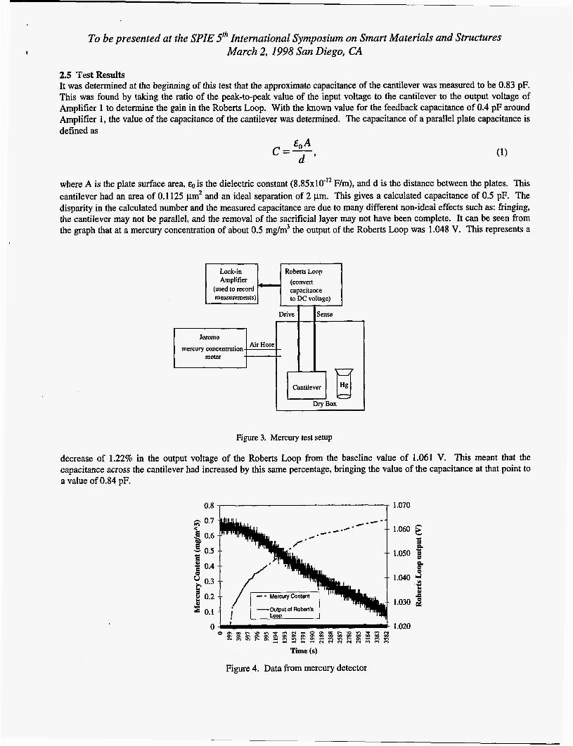
2.3 Mercury detector measurement Setup The items used to make these measurements were a small bottle with mercury, a Roberts Loop system, lock-in amplifier (SR850 from Stanford Research Systems), a Jerome mercury monitor (431-X for mercury content measurements), and a plastic dry box. The cantilever chip, whose legs were coated with 50 nm of gold, was mounted on a PC board with both sides of the capacitor, the plate and cantilever, connected to individual BNC connectors as shown in Fig. 3. The “sense” line connected the probe input on the Roberts Loop to the cantilever. The “drive” line connected the probe output of the Roberts Loop to the plate. Both of these connections were made using a BNC cable that entered the dry box through a hole. Both of these cables were kept very short in order to reduce the capacitance due to the cables. The DC output of the Roberts Loop
Compensation
Setpoint --I I ~-
level
:I! - . ~- : :1-: Bandpass 1 Amplifie 2
Rectifier
< _ _ _ _ _ _ _ _ _______: Analog
Cantilever 1ookHz multiplier
under test sinewave
Figure 2. Block diagram of the Roberts Loop electronics
was connected to an auxiliary input of the Lock-In Amplifier, which was used to record the output voltage of the Roberts Loop. The Jerome mercury concentration monitor was then connected to the dry box using an airtight connector. Next, the mercury source was placed such that the cantilever was between the source and the hole for the Jerome measurements. This was done so that the measurements of the mercury vapor would be done near the surface of the cantilever, which is the location of interest, and not right next to the source where the mercury content would be higher. A piece of wire that was connected to the cork was run out of the box above the bottle and allowed us to start and stop the input of mercury vapor.
2.4 Test Procedure The DC output voltage of the Roberts Loop was adjusted using the fine calibration to give an output voltage of approximately 1 V. The Lock-In Amplifier was configured to record the DC output voltage and to take measurements at a rate of two measurements each second with the Jerome measurement occurring once every minute. The first three and a half minutes of this test were used to form a baseline, this can be seen on the output data of Fig. 4. The recorded output voltages and Jerome measurements were then plotted as a function of time with all Jerome points between measured data points interpolated.
To be presented at the SPIE SIh International Symposium on Smart Materials and Structures t March 2,1998 San Diego, CA
Drive
Jerome mercury concentration - .
meter Air Hose
2.5 Test Results It was determined at the beginning of this test that the approximate capacitance of the cantilever was measured to be 0.83 pF. This was found by taking the ratio of the peak-to-peak value of the input voltage to the cantilever to the output voltage of Amplifier 1 to determine the gain in the Roberts Loop. With the known value for the feedback capacitance of 0.4 pF around Amplifier 1, the value of the capacitance of the cantilever was determined. The capacitance of a parallel plate capacitance is defined as
Sense
where A is the plate surface area, %is the dielectric constant (8.85~10-" F/m), and d is the distance between the plates. This cantilever had an area of 0.1 125 pm2 and an ideal separation of 2 pm. This gives a calculated capacitance of 0.5 pF. The disparity in the calculated number and the measured capacitance are due to many different non-ideal effects such as: fringing, the cantilever may not be parallel, and the removal of the sacrificial layer may not have been complete. It can be seen from the graph that at a mercury concentration of about 0.5 mg/m3 the output of the Roberts Loop was 1.048 V. This represents a
1-1 I RobertsLoop i Amplifier (convert
(used to record capacitance
Figure 3. Mercury test setup
decrease of 1.22% in the output voltage of the Roberts Loop from the baseline value of 1.061 V. This meant that the capacitance across the cantilever had increased by this same percentage, bringing the value of the capacitance at that point to a value of 0.84 pF.
0.8 1.070
1.060 E 1.050
w
B g.
E a 1.030 4
1.040 5
To be presented at the SPIE 5‘h International Symposium on Smart Materials and Structures I March 2, I998 San Diego, CA
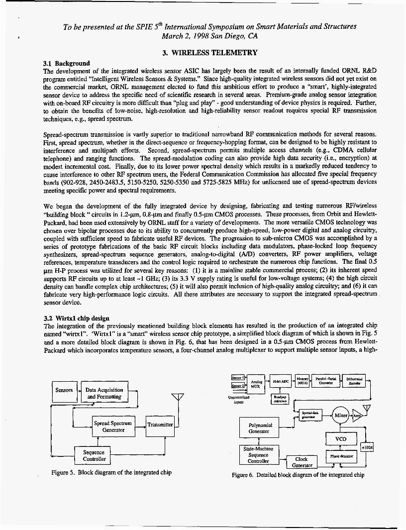
Sensors +
3. WIRELESS TELEMETRY 3.1 Background The development of the integrated wireless sensor ASIC has largely been the result of an internally funded ORNL, R&D program entitled “Intelligent Wireless Sensors & Systems.” Since high-quality integrated wireless sensors did not yet exist on the commercial market, ORNL management elected to fund this ambitious effort to produce a “smart’, highly-integrated sensor device to address the specific need of scientific research in several areas. Premium-grade analog sensor integration with on-board RF circuitry is more difficult than “plug and play” - good understanding of device physics is required. Further, to obtain the benefits of low-noise, high-resolution and high-reliability sensor readout requires special RF transmission techniques, e.g., spread spectrum.
Data Acquisition and Formatting
Spread-spectrum transmission is vastly superior to traditional narrowband RF communication methods for several reasons. First, spread spectrum, whether in the direct-sequence or frequency-hopping format, can be designed to be highly resistant to interference and multipath effects. Second, spread-spectrum permits multiple access channels (e.g., CDMA cellular telephone) and ranging functions. The spread-modulation coding can also provide high data security (i.e,, encryption) at modest incremental cost. Finally, due to its lower power spectral density which results in a markedly reduced tendency to cause interference to other RF spectrum users, the Federal Communication Commission has allocated five special frequency bands (902-928, 2450-2483.5, 5 150-5250, 5250-5350 and 5725-5825 MHz) for unlicensed use of spread-spectrum devices meeting specific power and spectral requirements.
9 t 4
- v , spread SPecmm - Transmitter -
We began the development of the fully integrated device by designing, fabricating and testing numerous RF/wireless “building block “ circuits in 1.2-pm, 0.8-pm and finally 0.5-pm CMOS processes. These processes, from Orbit and Hewlett- Packard, had been used extensively by ORNL staff for a variety of developments. The more versatile CMOS technology was chosen over bipolar processes due to its ability to concurrently produce high-speed, low-power digital and analog circuitry, coupled with sufficient speed to fabricate useful RF devices. The progression to sub-micron CMOS was accomplished by a series of prototype fabrications of the basic RF circuit blocks including data modulators, phase-locked loop frequency synthesizers, spread-spectrum sequence generators, analog-to-digital (An>) converters, RF power amplifiers, voltage references, temperature transducers and the control logic required to orchestrate the numerous chip functions. The final 0.5 pm H-P process was utilized for several key reasons: (1) it is a mainline stable commercial process; (2) its inherent speed supports RF circuits up to at least -1 GHz; (3) its 3.3 V supply rating is useful for low-voltage systems; (4) the high circuit density can handle complex chip architectures; (5) it will also permit inclusion of high-quality analog circuitry; and (6) it can fabricate very high-performance logic circuits. All these attributes are necessary to support the integrated spread-spectrum sensor device.
Controller
3.2 Wirtxl chip design The integration of the previously mentioned building block elements has resulted in the production of an integrated chip named “wirtxl”. ‘Wirtxl” is a “smart” wireless sensor chip prototype, a simplified block diagram of which is shown in Fig. 5 and a more detailed block diagram is shown in Fig. 6, that has been designed in a 0.5-pm CMOS process from Hewlett- Packard which incorporates temperature sensors, a four-channel analog multiplexer to support multiple sensor inputs, a high-
UncnmmiUed 1
Generator
T State-Machine
Controller Sequence Phasede(eetor
Figure 6. Detailed block diagram of the integrated chip
To be presented at the SPIE 5'h International Symposium on Smart Materials and Structures 1 March 2,1998 San Diego, CA
perfccmance 10-bit AID converter with voltage reference, a programmable spread-spectrum generator with selectable families of polynomials, an integrated state-machine system controller, high-speed data modulator, and output RF power amplifier. The chip utilizes an internal sequence controller that cycles the device through an entire data acquisition-transmit routine at a regular interval. The fabricated device has been successfully tested and verified to be operational. The various sub-systems are described below.
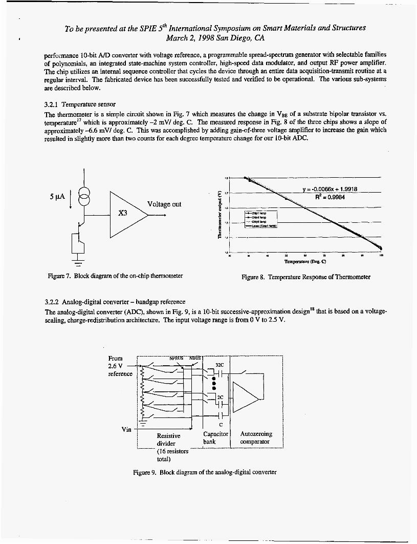
3.2.1 Temperature sensor The thermometer is a simple circuit shown in Fig. 7 which measures the change in V B ~ of a substrate bipolar transistor vs. temperature" which is approximately -2 mV/ deg. C. The measured response in Fig. 8 of the three chips shows a slope of approximately -6.6 mV/ deg. C. This was accomplished by adding gain-of-three voltage amplifier to increase the gain which resulted in slightly more than two counts for each degree temperature change for our 10-bit ADC.
out
Figure 7. Block diagram of the on-chip thermometer Figure 8. Temperature Response of Thermometer
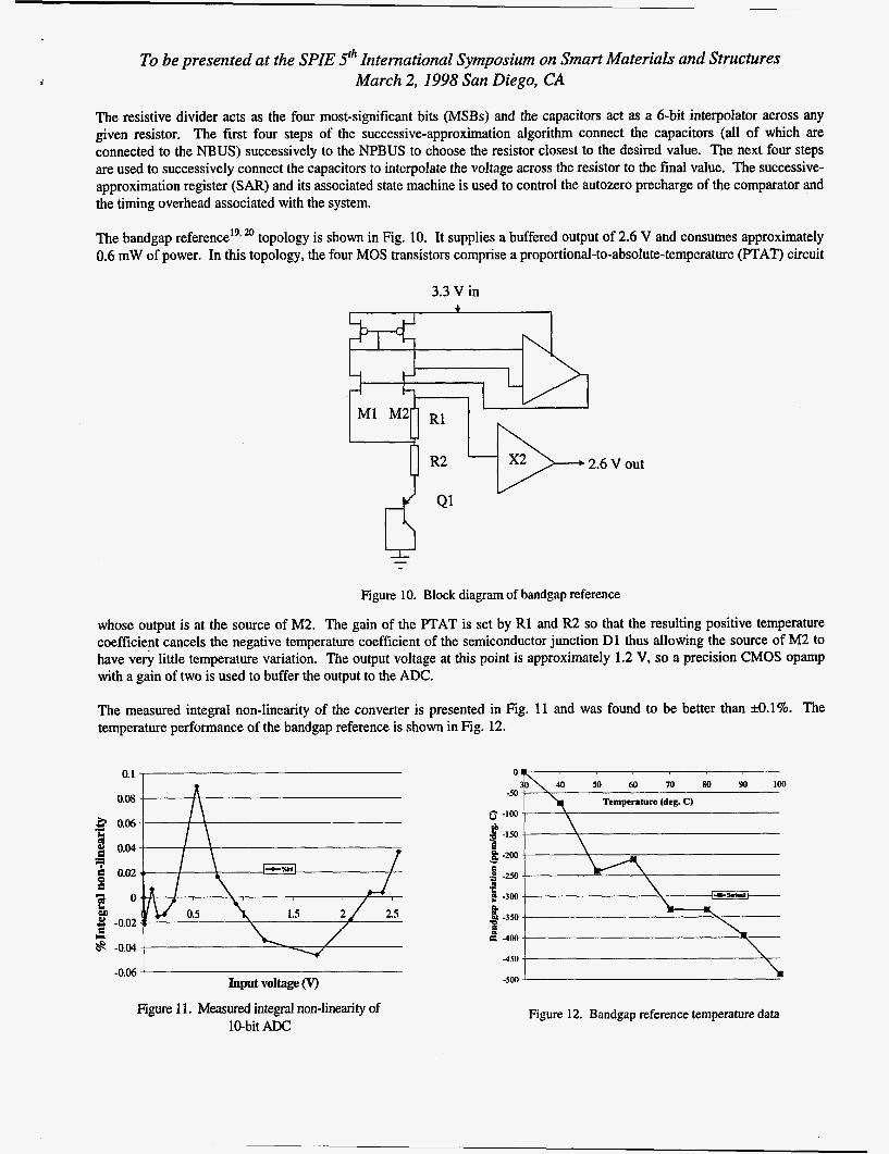
3.2.2 Analog-digital converter - bandgap reference The analog-digital converter (ADC), shown in Fig. 9, is a 10-bit successive-approximation design" that is based on a voltage- scaling, charge-redistribution architecture. The input voltage range is from 0 V to 2.5 V.
,..,
i i ; 1 i
i
bank 1 comparator j i
l.... __.._ _.-_ ___- ~ -__-.__-______.__._.. ___ ._._ ......... ! divider (16 resistors :. ..... _._... total)
Figure 9. Block diagram of the analog-digital converter
To be presented at the SPIE Sth International Symposium on Smart Materials and Structures March 2,1998 Sun Diego, CA
The resistive divider acts as the four most-significant bits (MSBs) and the capacitors act as a 6-bit interpolator across any given resistor. The first four steps of the successive-approximation algorithm connect the capacitors (all of which are connected to the NBUS) successively to the NPBUS to choose the resistor closest to the desired value. The next four steps are used to successively connect the capacitors to interpolate the voltage across the resistor to the final value. The successive- approximation register (SAR) and its associated state machine is used to control the autozero precharge of the comparator and the timing overhead associated with the system.
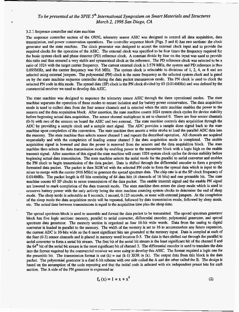
The bandgap topology is shown in Fig. 10. It supplies a buffered output of 2.6 V and consumes approximately 0.6 mW of power. In this topology, the four MOS transistors comprise a proportional-to-absolute-temperature (PTAT) circuit
3.3 V in +
2.6 v out
Figure 10. Block diagram of bandgap reference
whose output is at the source of M2. The gain of the PTAT is set by R1 and R2 so that the resulting positive temperature coefficient cancels the negative temperature coefficient of the semiconductor junction D1 thus allowing the source of M2 to have very little temperature variation. The output voltage at this point is approximately 1.2 V, so a precision CMOS opamp with a gain of two is used to buffer the output to the ADC.
The measured integral non-linearity of the converter is presented in Fig. 11 and was found to be better than &l%. The temperature performance of the bandgap reference is shown in Fig. 12.
0.1 , 0.08
P 0.06 'E 3 0.04
3 0.02 a a 0 kp
-0.02 $ -0.04
-0.06 ' Input voltage 0
Figure 1 1. Measured integral non-linearity of 10-bit ADC
Temperahre (deg. C )
2 400- \ -450 1 1 .
k -500 ' Figure 12. Bandgap reference temperature data
To be presented at the SPIE Sth International Symposium on Smart Materials and Structures 1 March 2,1998 San Diego, CA
3.22 Sequence controller and state machine The sequence controller section of the ORNL, telemetry sensor ASIC was designed to control all data acquisition, data transmission, and power conservation operations. The controller sequence block (Figs. 5 and 6) has two sections: the clock generator and the state machine. The clock generator was designed to accept the external clock input and to provide the required clocks for the operation of the ASIC. The external clock was specified to be four times the frequency required for the basic system clock and phase detector (PD) reference clock. A constant divide by four on the input was used to provide this ratio and thus ensured a very stable and symmetrical clock as the reference. The PD reference clock was selected to be a ratio of 1024 with the target carrier frequency. The current external clock is 3.579 MHz, the system and PD reference is thus 0.895MHz, and the carrier frequency was 916 MHz. The system clock is selectable to divisions of 1, 2, 4, or 8 and are selected using external jumpers. The polynomiaI (PN) clock is the same frequency as the selected system clock and is gated on by the state machine sequence controller during the data packet transmission mode. The PN clock is used to clock the selected PN code in this mode. The spread data (SP) clock is the PN clock divided by 63 (0.014MHz) and was defined by the commercial receiver we used to develop this ASIC.
The state machine was designed to sequence the telemetry sensor ASIC through the three operational modes. The state machine separates the operation of these modes to ensure isolation and for battery power conservation. The data acquisition mode is used to collect data from the four sensor channels and is selected when the state machine enables the power to the sensors and the data acquisition block. After assertion, the state machine counts 1024 system clock cycles for device stability before beginning actual data acquisition. The sensor channel multiplexer is set to channel 0. There are four sensor channels (0-3) with two of the sensors on board the ASIC and two external. The state machine controls data acquisition through the ADC by providing a sample clock and a sample start signal. The ADC provides a sample done signal back to the state machine upon completion of the conversion. The state machine then asserts a write strobe to load the parallel ADC data into the memory. The state machine then selects sensor channel 1 and repeats the described operation. All channels are acquired sequentially and with the completion of loading sensor channel 3 the data acquisition mode is completed. The enable acquisition signal is lowered and thus the power is removed from the sensors and the data acquisition block. The state machine then selects the data transmission mode by enabling power to the transmitter block with a logic high on the enable transmit signal. After assertion of this signal the state machine will count 1024 system clock cycles for device stability before beginning actual data transmission. The state machine selects the serial mode for the parallel to serial converter and enables the PN clock to begin transmission of the data packet, Data is shifted through the differential encoder to form a properly formatted data packet. The packet is then XOR’ed with the selected PN code to form the spread data which is input to the mixer to merge with the carrier (916 MHz) to generate the spread spectrum data. The chip rate is at the SP clock frequency of 0.014MHz. The packet length is 65 bits consisting of 64 data bits (4 channels of 16 bits) and one preamble bit. The state machine counts 65 SP clocks to sense transmission of the data packet. The enable transmit signal and the enable PN signal are lowered to mark completion of the data transmit mode. The state machine then enters the sleep mode which is used to conserve battery power with the only activity being the state machine counting system clocks to determine the end of sleep mode. The sleep mode is selectable as 8 seconds, 1 second, 0.125 seconds, or none with external jumpers. At the completion of the sleep mode the data acquisition mode will be repeated, followed by data transmission mode, followed by sleep mode, etc. The actual time between transmissions is equal to the acquisition time plus the sleep time.
The spread spectrum block is used to assemble and format the data packet to be transmitted. The spread spectrum generator block has five logic sections: memory, parallel to serial converter, differential encoder, polynomial generator, and spread spectrum data generator. The memory section is organized as four 16-bit wide words. Data from the analog to digital converter is loaded in parallel to the memory. The width of the memory is set to 16 to accommodate any future expansion, the current ADC is 10-bits wide so the 6 most significant bits are grounded at the memory input. Data is sampled at each of the four (0-3) sensor channels and is placed in memory word location 0-3. The data is then shifted out through the parallel to serial converter to form a serial bit stream. The first bit of the serial bit stream is the least significant bit of the channel 0 and the 64* bit of the serial bit stream is the most significant bit of channel 3. The differential encoder is used to translate the data into the format required by the commercial receiver we were using to develop this ASIC. The format required a logic one for the preamble bit. The transmission format is out (k) = out (k-1) XOR in (k). The output data from this block is the data packet. The polynomial generator is a dual 6-bit scheme with one side called the A and the other called the B. The design is based on the assumption of the code repeating and that the initial code is selected with six independent preset bits for each section. The A side of the PN generator is expressed as
fa (x) = 1 + x f x6 (2)
To be presented at the SPIE Sth International Symposium on Smart Materials and Structures March 2, I998 San Diego, CA
Charge Pump Passive Lag b Phase-Frequency,---) Low-Pass
Frequency Detector Filter
The presets are hard wired to logic high, thus the A section initialization is preset. The output of the A is known as the A maximal length sequence (AMLS). The B side of the PN generator is expressed as
+ vco RF
The presets for the B section are selected as either all logic highs or via six external parameters. Jumpers define the preset selection and the polarity of the six external present bits. The output of the B is known as the B maximal length sequence (BMLS). The GOLD code output is generated from the XOR of the AMLS and BMLS. The spread data generator is used to XOR the selected PN code with the data packet to produce the spread data sent to the mixer. The spread data generator can selected one of four different PN codes. These codes are GOLD, AMLS, BMLS, and external code. The external parameters for the code selection are jumper selectable.
+ 1024
3.2.4 RF Section The RF section consists of a voltage-controlled oscillator, a phase-locked loop, a mixer and an amplifier and is designed for operation in the 902-928 MHz band. Since the RF section draws considerable power when operating, its components can be shut down by the sequence controller to conserve power. The mixer is an active doubly balanced CMOS mixer based upon the Gilbert cell multiplier topologyz1. The input from the spread-data generator is fully differential while the input from the VCO is quasi-differential, having the VCO output applied to one terminal and a dc bias applied to the complementary terminal. The single-ended output is capable of driving a 50-ohm load, which in this case is the input impedance of the RF amplifier.
4
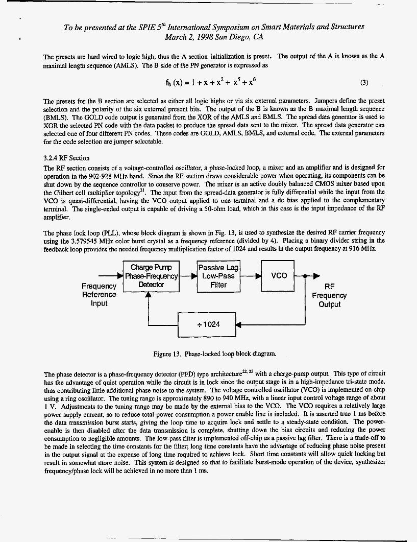
Figure 13. Phase-locked loop block diagram.
The phase detector is a phase-frequency detector (PED) type architecturez2Tz3 with a charge-pump output. This type of circuit has the advantage of quiet operation while the circuit is in lock since the output stage is in a high-impedance tri-state mode, thus contributing little additional phase noise to the system. The voltage controlled oscillator (VCO) is impIemented on-chip using a ring oscillator. The tuning range is approximately 890 to 940 MHz, with a linear input control voltage range of about 1 V. Adjustments to the tuning range may be made by the external bias to the VCO. The VCO requires a relatively large power supply current, so to reduce total power consumption a power enable line is included. It is asserted true 1 ms before the data transmission burst starts, giving the loop time to acquire lock and settle to a steady-state condition. The power- enable is then disabled after the data transmission is complete, shutting down the bias circuits and reducing the power consumption to negligible amounts. The Iow-pass filter is implemented off-chip as a passive lag filter. There is a trade-off to be made in selecting the time constants for the filter; long time constants have the advantage of reducing phase noise present in the output signal at the expense of long time required to achieve lock. Short time constants will allow quick locking but result in somewhat more noise. This system is designed so that to facilitate burst-mode operation of the device, synthesizer frequency/phase lock will be achieved in no more than 1 ms.
To be presented at the SPIE 5'h International Symposium on Smart Materials and Structures March 2,1998 San Diego, CA
BIT SETTINGS CYCLE TIME (l=high, O=low)
0-0 8 s 0- 1 1 s 1-0 0.147 s 1-1 0.007 s
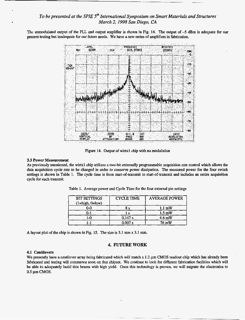
The unmodulated output of the PLL and output amplifier is shown in Fig. 14. The output of -5 dBm is adequate for our present testing but inadequate for our future needs. We have a new series of amplifiers in fabrication.
AVERAGE POWER
1.1 mW 1.5 mW 4.6mW 76 mW
Figure 14. Output of wirtxl chip with no modulation
3.3 Power Measurement As previously mentioned, the wirtxl chip utilizes a two-bit externally programmable acquisition rate control which allows the data acquisition cycle rate to be changed in order to conserve power dissipation. The measured power for the four switch settings is shown in Table 1. The cycle time is from start-of-transmit to start-of-transmit and includes an entire acquisition cycle for each transmit.
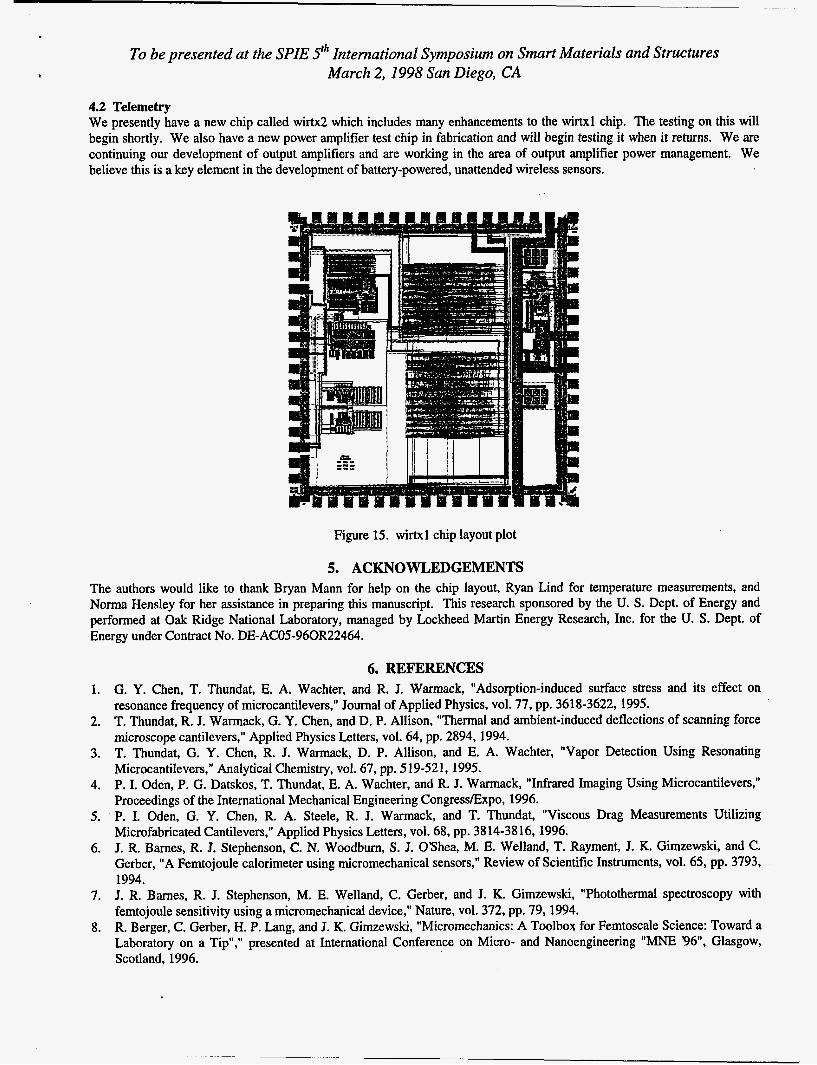
A layout plot of the chip is shown in Fig. 15. The size is 3.1 mm x 3.1 mm.
4. FUTUREWORK 4.1 Cantilevers We presently have a cantilever array being fabricated which will match a 1.2 pm CMOS readout chip which has already been fabricated and testing will commence soon on that chipset. We continue to look for different fabrication facilities which will be able to adequately build thin beams with high yield. Once this technology is proven, we will migrate the electronics to 0.5 pm CMOS.
k
To be presented at the SPIE Sth International Symposium on Smart Materials and Structures March 2,1998 San Diego, CA
4.2 Telemetry We presently have a new chip called wirtx2 which includes many enhancements to the wirtxl chip. The testing on this will begin shortly. We also have a new power amplifier test chip in fabrication and will begin testing it when it returns. We are continuing our development of output amplifiers and are working in the area of output amplifier power management. We believe this is a key element in the development of battery-powered, unattended wireless sensors.
Figure 15. wirtxl chip layout plot
5. ACKNOWLEDGEMENTS The authors would like to thank Bryan Mann for help on the chip layout, Ryan Lind for temperature measurements, and Norma Hensley for her assistance in preparing this manuscript. This research sponsored by the U. S. Dept. of Energy and performed at Oak Ridge National Laboratory, managed by Lockheed Martin Energy Research, Inc. for the U. S. Dept. of Energy under Contract No. DE-ACO5-96OR22464.
1.
2.
3.
4.
5.
6.
7.
8.
6. REFERENCES G. Y. Chen, T. Thundat, E. A. Wachter, and R. J. Warmack, "Adsorption-induced surface stress and its effect on resonance frequency of microcantilevers," Journal of Applied Physics, vol. 77, pp. 361 8-3622, 1995. T. Thundat, R. J. Warmack, G. Y. Chen, and D. P. Allison, "Thermal and ambient-induced deflections of scanning force microscope cantilevers," Applied Physics Letters, vol. 64, pp. 2894, 1994. T. Thundat, G. Y. Chen, R. J. Warmack, D. P. Allison, and E. A. Wachter, "Vapor Detection Using Resonating Microcantilevers," Analytical Chemistry, vol. 67, pp. 5 19-521, 1995. P. I. Oden, P. G. Datskos, T. Thundat, E. A. Wachter, and R. J. Warmack, "Infrared Imaging Using Microcantilevers," Proceedings of the International Mechanical Engineering Congress/Expo, 1996. P. I. Oden, G. Y. Chen, R. A. Steele, R. J. Warmack, and T. Thundat, "Viscous Drag Measurements Utilizing Microfabricated Cantilevers," Applied Physics Letters, vol. 68, pp. 3814-3816, 1996. J. R. Barnes, R. J. Stephenson, C. N. Woodburn, S. J. OShea, M. E. Welland, T. Rayment, J. K. Gimzewski, and C. Gerber, "A Femtojoule calorimeter using micromechanical sensors," Review of Scientific Instruments, vol. 65, pp. 3793, 1994. J. R. Barnes, R. J. Stephenson, M. E. Welland, C. Gerber, and J. K. Gimzewski, "Photothermal spectroscopy with femtojoule sensitivity using a micromechanical device," Nature, vol. 372, pp. 79, 1994. R. Berger, C. Gerber, H. P. Lang, and J. K. Gimzewski, "Micromechanics: A Toolbox for Ferntoscale Science: Toward a Laboratory on a Tip"," presented at International Conference on Micro- and Nanoengineering "MNE 96, Glasgow, Scotland, 1996.
To be presented at the SPIE Sth International Symposium on Smart Materials and Structures March 2,1998 San Diego, CA
9.
10. D. Sarid, Scanning Force Microscopy. New York: Oxford University Press, 1991. 11. T. Thundat, P. I. Oden, and R. J. Warmack, "Microcantilever Sensors," Microscale Thermophysical Engineering, vol. 1,
12. P. I. Oden, E. A. Wachter, P. G. Datskos, T. Thundat, and R. J. Warmack, "Optical and Infrared Detection Using
13. P. I. Oden, P. G. Datskos, T. Thundat, E. A. Wachter, and R. J. Warmack, "Infrared Detection Using Microcantilevers,"
14. E. A. Wachter, T. Thundat, P. G. Datskos, P. I. Oden, S. L. Sharp, and R. J. Warmack, "Remote Optical Detection Using
15. P. I. Oden, T. Thundat, and R. J. Warmack, "Electrochemical Deposition Induced Stress Measurements on a
16. Advanced Instrumentation for Reflood Studies, Internal ORNL Documents. 17. P. R. Gray and R. G. Meyer, Analysis and Design of Analog Integrated Circuits, Second Edition, John Wiley and Sons,
18. B. Fotouhi and D. A. Hodges, "High-Resolution A/D Conversion in MOSLSI," IEEE Journal of Solid State Circuits,
19. P. R. Gray and R. G. Meyer, Analysis and Design of Analog Integrated Circuits, Second Edition, John Wiley and Sons,
20. R. J. Reay, E. H. Klaassen, and G, T. A. Kovacs, "A Micromachined Low-Power Temperature-Regulated Bandgap
21. B. Gilbert, "A Precise Four-Quadrant Multiplier with Subnanosecond Response," IEEE Journal of Solid State Circuits,
22. Wolaver, Phase-Locked LOOD Circuit Design, 199 1, Prentice Hall, Englewood Cliffs, New Jersey 07632. 23. Best, Phase-Locked Loous, 1997, McGraw-Hill.
E. Meyer, J. K. Ginzewski, C. Gerber, and R. R. Schlittler, "Micromechanical calorimeter with picojoule sensitivity," presented at Ultimate Limits of Fabrication and Measurement, 1995.
pp. 185-199, 1997.
Microcantilevers," presented at SPIE - The International Society for Optical Engineers, Orlando, FL, 1996.
presented at ASME - Thermal Imaging conference, Atlanta, Georgia, 1996.
Microcantilevers," Review of Scientific Instruments, 1996.
Microcantilever Investigated with Cyclic Voltammetry," Scanning Microscopy, vol. 10, 1997.
New York, 1984, p. 290.
Vol. SC-14, No. 6, December, 1979, pp. 920-925.
New York, 1984, p. 289-293.
Voltage Reference," IEEE Journal of Solid State Circuits, Vol. 30, No. 12, December, 1995, pp. 1374-1381.
December, 1968, pp. 365-373.
Report Number
Publ. Date (1 1)
Sponsor Code (18) a o e ,? XF
DOE