Embed Size (px)
Citation preview
© CEA. All rights reserved
MEMS R&D at Leti
André ROUZAUD, Deputy Head of Department
Jean-Philippe POLIZZI, Microsystems Program manager
iNEMI Research seminar Series
© CEA. All rights reserved
Summary
Short overview of Léti
The context of MEMS
The next steps in MEMS: Generic platforms
Physical sensors
Chemical sensors
Conclusion
MEMS webinar | 2
© CEA. All rights reserved
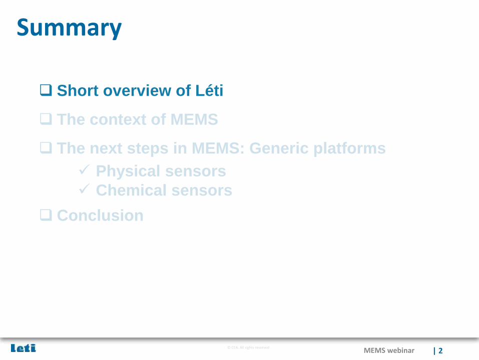
Leti key figures
CEA Institute founded in 1967
Director : Dr Laurent Malier
1700 collaborators1 150 permanent staff200 PhD and post-doc, 40 nationalities
2200 patents286 registered in 201240 % under licensing
Budget : 250 M€CapEx : 40M€75% from external revenue
8 000m² clean roomsFor 200 and 300mm wafer fab, operated 24/7
MEMS webinar | 3
© CEA. All rights reserved
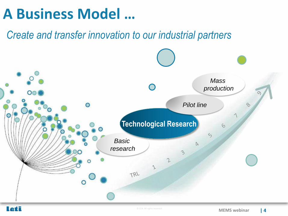
A Business Model …Create and transfer innovation to our industrial partners
Basic
research
Technological Research
Pilot line
Mass
production
MEMS webinar | 4
© CEA. All rights reserved
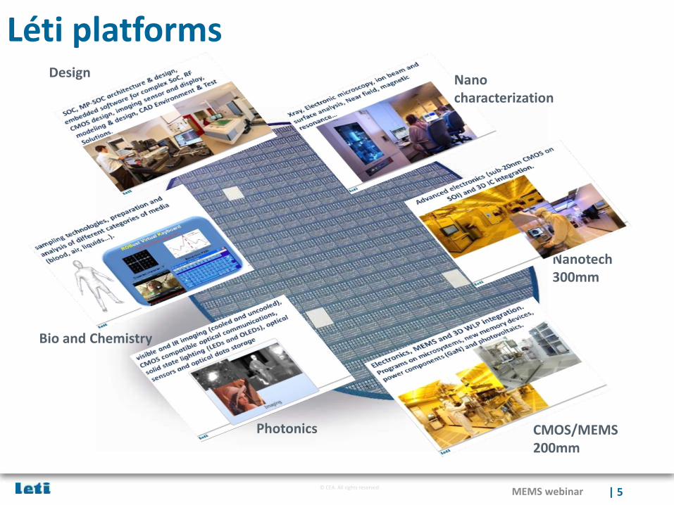
Léti platforms
CMOS/MEMS 200mm
Nanotech 300mm
Bio and Chemistry
Photonics
Design Nano characterization
MEMS webinar | 5
© CEA. All rights reserved
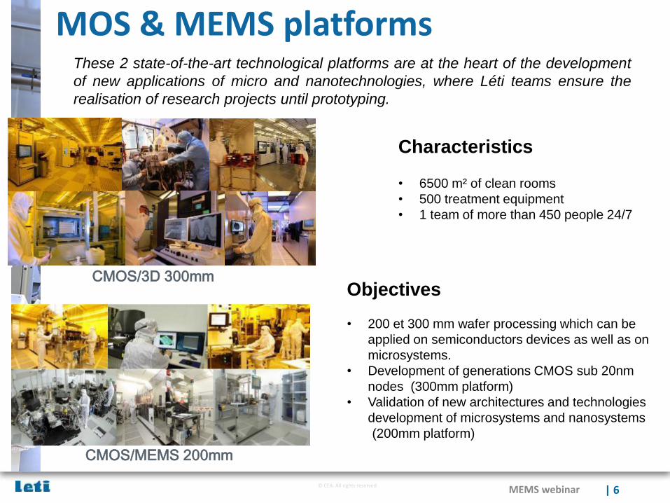
These 2 state-of-the-art technological platforms are at the heart of the development
of new applications of micro and nanotechnologies, where Léti teams ensure the
realisation of research projects until prototyping.
Characteristics
• 6500 m² of clean rooms
• 500 treatment equipment
• 1 team of more than 450 people 24/7
Objectives
• 200 et 300 mm wafer processing which can be
applied on semiconductors devices as well as on
microsystems.
• Development of generations CMOS sub 20nm
nodes (300mm platform)
• Validation of new architectures and technologies
development of microsystems and nanosystems
(200mm platform)
MOS & MEMS platforms
CMOS/3D 300mm
CMOS/MEMS 200mm
MEMS webinar | 6
© CEA. All rights reserved
Summary
Short overview of Léti
The context of MEMS
The next steps in MEMS: Generic platforms
Physical sensors
Chemical sensors
Conclusion
MEMS webinar | 7
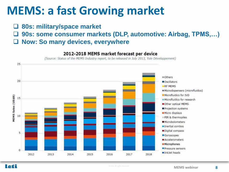
© CEA. All rights reservedMEMS webinar 8
MEMS: a fast Growing market 80s: military/space market
90s: some consumer markets (DLP, automotive: Airbag, TPMS,…)
Now: So many devices, everywhere
© CEA. All rights reserved
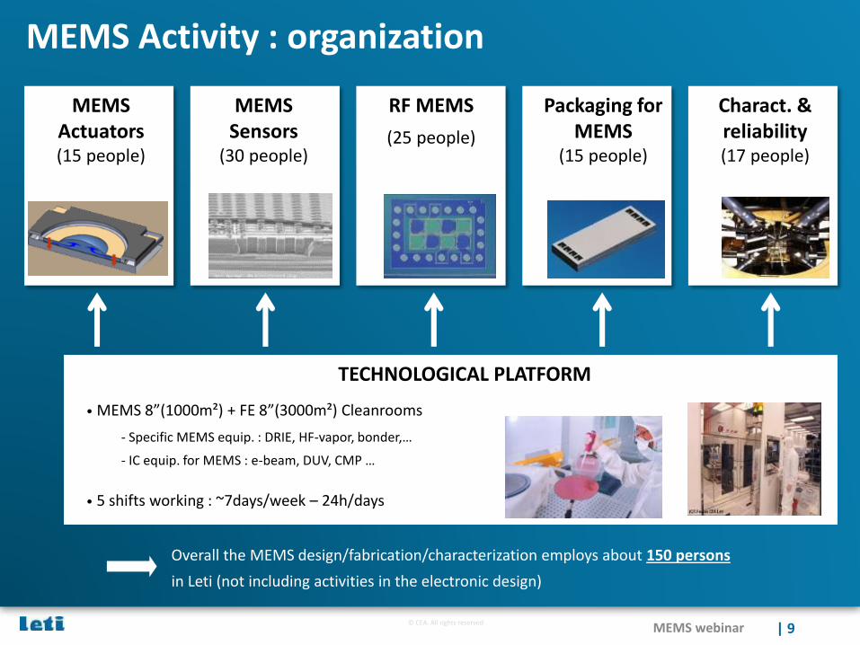
MEMS Activity : organization
Overall the MEMS design/fabrication/characterization employs about 150 persons
in Leti (not including activities in the electronic design)
Charact. & reliability (17 people)
Packaging for MEMS
(15 people)
RF MEMS
(25 people)
MEMS Actuators(15 people)
MEMS Sensors
(30 people)
TECHNOLOGICAL PLATFORM
• MEMS 8”(1000m²) + FE 8”(3000m²) Cleanrooms
- Specific MEMS equip. : DRIE, HF-vapor, bonder,…
- IC equip. for MEMS : e-beam, DUV, CMP …
• 5 shifts working : ~7days/week – 24h/days
MEMS webinar | 9
© CEA. All rights reserved
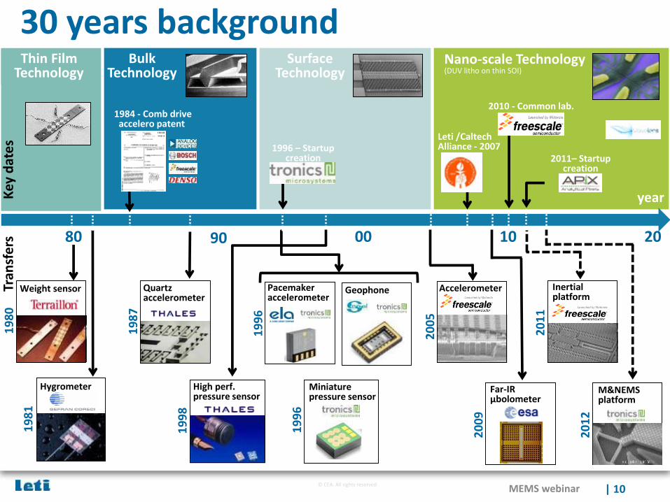
Thin Film Technology
Bulk Technology
Surface Technology
Nano-scale Technology(DUV litho on thin SOI)
30 years background
80 90 00
year
10 20
Tran
sfe
rsK
ey d
ate
s
1984 - Comb drive accelero patent
19
81
Hygrometer
Quartz accelerometer
19
87
Weight sensor
19
80
Pacemaker accelerometer
Geophone
19
96
Miniature pressure sensor
19
96
Accelerometer
20
05
1996 – Startup creation 2011– Startup
creation
Leti /Caltech Alliance - 2007
2010 - Common lab.
M&NEMS platform
20
12
Far-IR µbolometer
20
09
High perf. pressure sensor
19
98
Inertial platform
20
11
MEMS webinar | 10
© CEA. All rights reserved
Summary
Short overview of Léti
The context of MEMS
The next steps in MEMS: Generic platforms
Physical sensors
Chemical sensors
Conclusion
MEMS webinar | 11
© CEA. All rights reserved
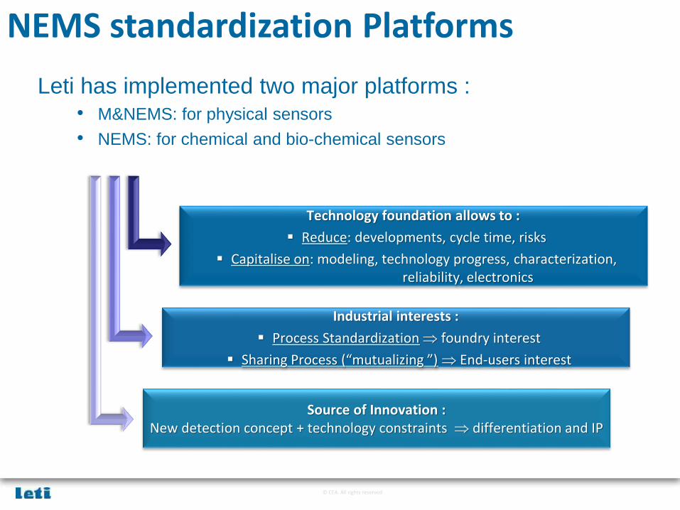
NEMS standardization Platforms
Leti has implemented two major platforms :• M&NEMS: for physical sensors
• NEMS: for chemical and bio-chemical sensors
Technology foundation allows to :
Reduce: developments, cycle time, risks
Capitalise on: modeling, technology progress, characterization, reliability, electronics
Industrial interests :
Process Standardization foundry interest
Sharing Process (“mutualizing ”) End-users interest
Source of Innovation : New detection concept + technology constraints differentiation and IP
© CEA. All rights reserved
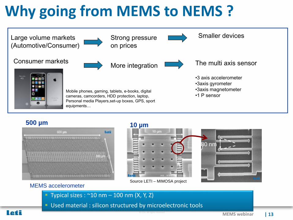
Why going from MEMS to NEMS ?
1 µm
Typical sizes : ~10 nm – 100 nm (X, Y, Z)
Used material : silicon structured by microelectronic tools
MEMS accelerometer
500 µm
80 nm
10 µm
Source LETI – MIMOSA project
Large volume markets
(Automotive/Consumer)
Strong pressure
on prices
Smaller devices
Consumer marketsMore integration The multi axis sensor
•3 axis accelerometer
•3axis gyrometer
•3axis magnetometer
•1 P sensorMobile phones, gaming, tablets, e-books, digital
cameras, camcorders, HDD protection, laptop,
Personal media Players,set-up boxes, GPS, sport
equipments…
MEMS webinar | 13
© CEA. All rights reserved
Miniaturization issuesP
erfo
rm
an
ce
s
MEMS Size
Ma
cro
scop
ic
se
nso
rM
acro
scop
ic
gM 2= g1000
M7
10.5
M7
.50000
M
Few cm² Few mm² 1 mm² 0,1 mm²
Electromagnet
ic detection
New design
Bu
lk te
ch
no
log
y
Piezo or
electrostatic out of
plane detection
Surf
ace technolo
gy
New design
Electrostatic in
plane detection
New design
?
?
Nano-Wire detection ?
M&
NE
MS
Performances
MEMS webinar | 14
© CEA. All rights reserved
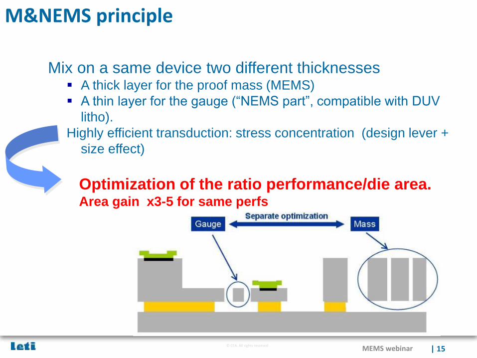
Optimization of the ratio performance/die area. Area gain x3-5 for same perfs
Mix on a same device two different thicknesses A thick layer for the proof mass (MEMS)
A thin layer for the gauge (“NEMS part”, compatible with DUV
litho).
Highly efficient transduction: stress concentration (design lever +
size effect)
M&NEMS principle
MEMS webinar | 15
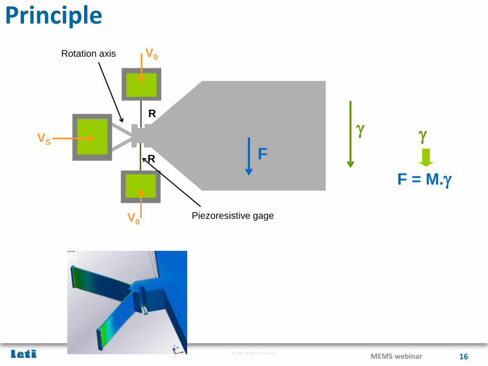
© CEA. All rights reservedMEMS webinar 16
Piezoresistive gage
Rotation axis
Seismic mass
Principle
VSg
V0
R
V0
R
g
F = M.g
F
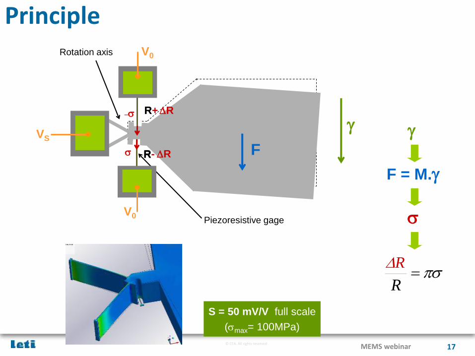
© CEA. All rights reservedMEMS webinar 17
Piezoresistive gage
Rotation axis
Seismic mass
Principle
VSg
V0
R
s
S = 50 mV/V full scale
(smax= 100MPa)
s=
R
RR
V0
R
s R- R
-s R+R
g
F = M.g
F
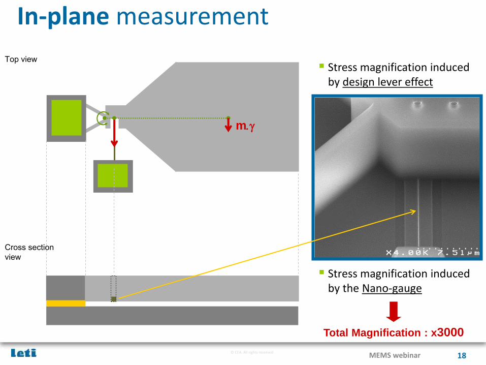
© CEA. All rights reservedMEMS webinar 18
Stress magnification induced by design lever effect
m.g
In-plane measurement
Stress magnification induced by the Nano-gauge
Total Magnification : x3000
Top view
Cross section
view
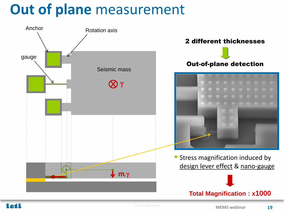
© CEA. All rights reservedMEMS webinar 19
2 different thicknesses
Out-of-plane detection
Rotation axis
m.g
Out of plane measurementAnchor
g
Seismic mass
gauge
Stress magnification induced by design lever effect & nano-gauge
Total Magnification : x1000
© CEA. All rights reservedMEMS webinar 20
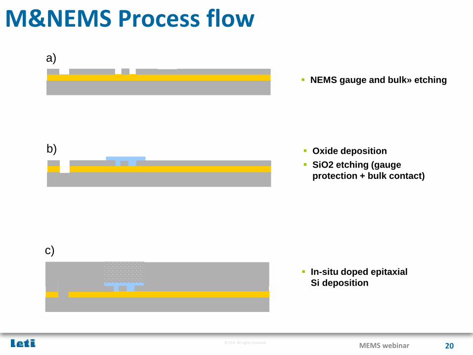
M&NEMS Process flow
NEMS gauge and bulk» etching
Oxide deposition
SiO2 etching (gauge
protection + bulk contact)
In-situ doped epitaxial
Si deposition
a)
b)
c)
© CEA. All rights reservedMEMS webinar 21
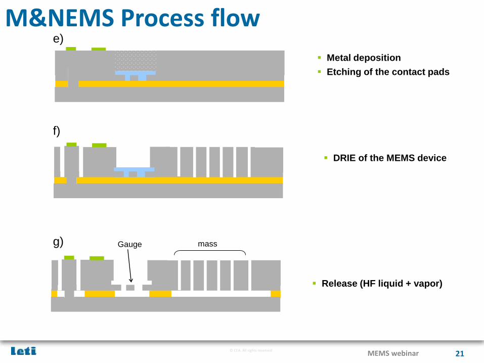
M&NEMS Process flow
Release (HF liquid + vapor)
Metal deposition
Etching of the contact pads
DRIE of the MEMS device
mass
e)
f)
g) Gauge
© CEA. All rights reserved
250nm
250nm
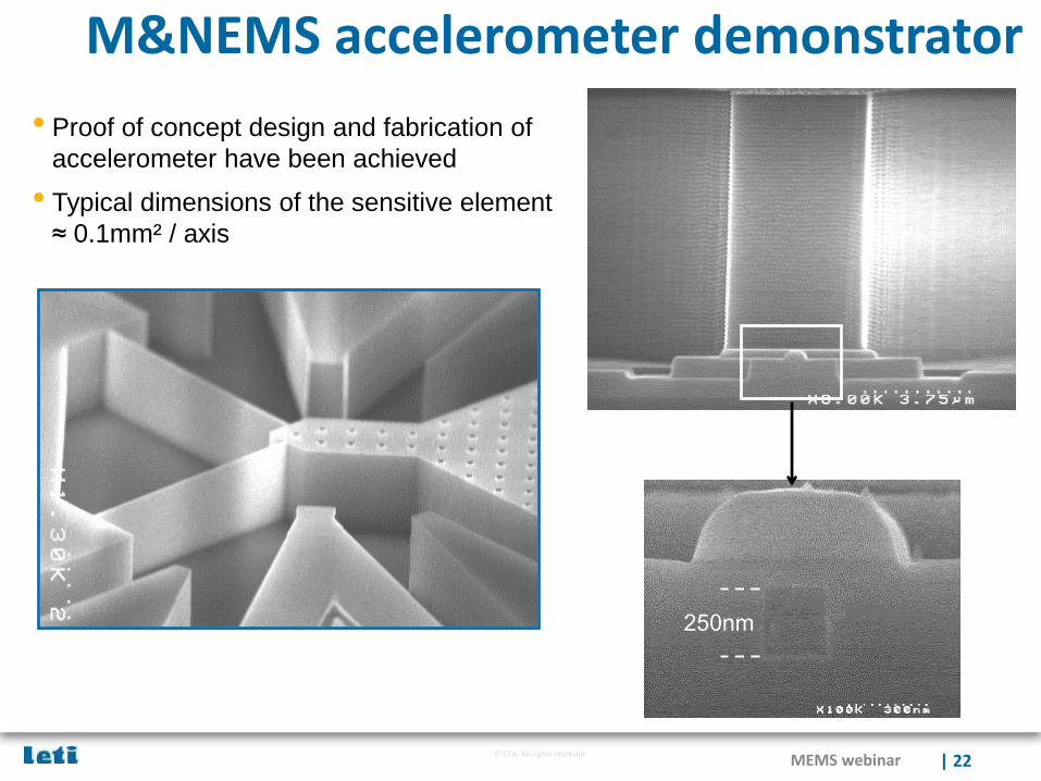
M&NEMS accelerometer demonstrator
15µm
• Proof of concept design and fabrication of
accelerometer have been achieved
• Typical dimensions of the sensitive element
≈ 0.1mm² / axis
MEMS webinar | 22
© CEA. All rights reserved
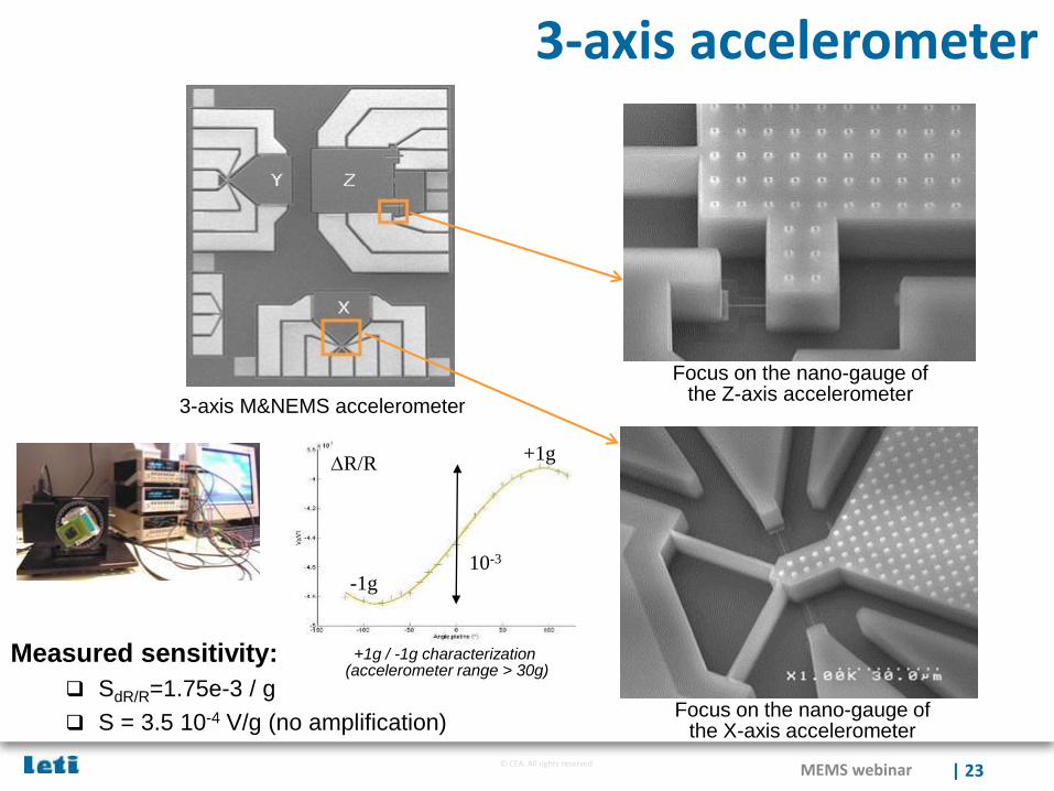
3-axis M&NEMS accelerometer
R/R
10-3
+1g
-1g
Focus on the nano-gauge of the Z-axis accelerometer
Focus on the nano-gauge of the X-axis accelerometer
+1g / -1g characterization(accelerometer range > 30g)
3-axis accelerometer
Measured sensitivity:
SdR/R=1.75e-3 / g
S = 3.5 10-4 V/g (no amplification)
MEMS webinar | 23
© CEA. All rights reserved
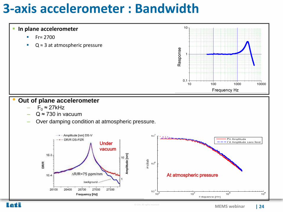
3-axis accelerometer : Bandwidth
In plane accelerometer
Fr= 2700
Q ≈ 3 at atmospheric pressure
• Out of plane accelerometer– F0 ≈ 27kHz
– Q ≈ 730 in vacuum
– Over damping condition at atmospheric pressure.
Under
vacuum
At atmospheric pressure
MEMS webinar | 24
© CEA. All rights reserved
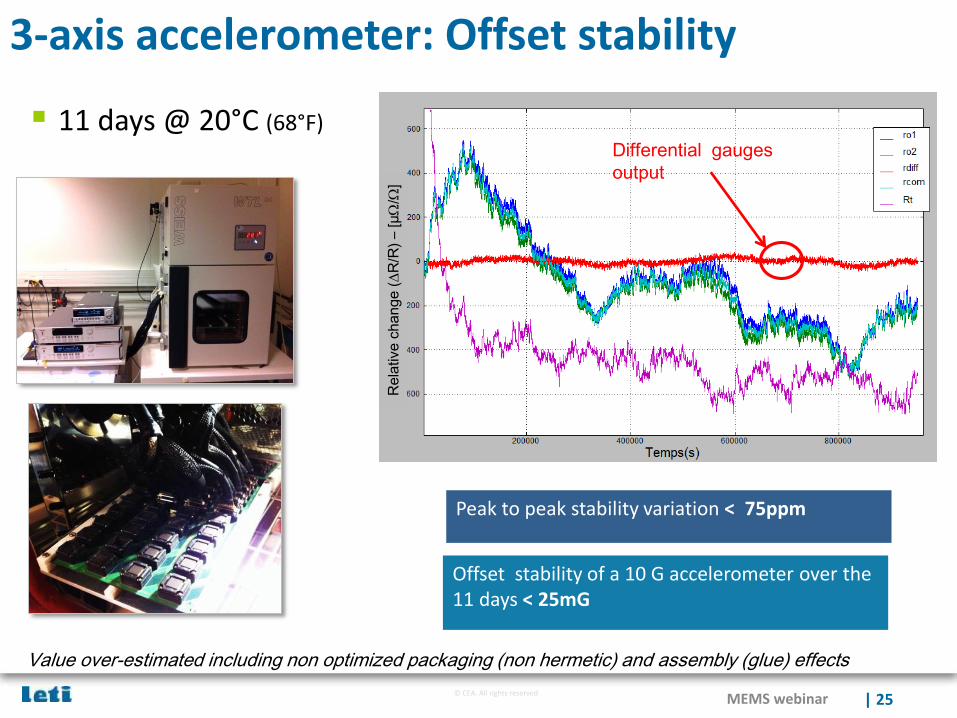
3-axis accelerometer: Offset stability
Peak to peak stability variation < 75ppm
Re
lative c
han
ge
(
R/R
) –
[µW
/W]
Offset stability of a 10 G accelerometer over the 11 days < 25mG
Differential gauges
output
11 days @ 20°C (68°F)
Value over-estimated including non optimized packaging (non hermetic) and assembly (glue) effects
MEMS webinar | 25
© CEA. All rights reserved
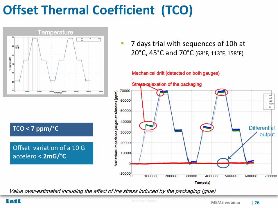
Offset Thermal Coefficient (TCO)
7 days trial with sequences of 10h at 20°C, 45°C and 70°C (68°F, 113°F, 158°F)
Temperature
cycle
Value over-estimated including the effect of the stress induced by the packaging (glue)
Mechanical drift (detected on both gauges)
-
Stress relaxation of the packaging
TCO < 7 ppm/°C
Offset variation of a 10 G accelero < 2mG/°C
Differential
output
MEMS webinar | 26
© CEA. All rights reserved
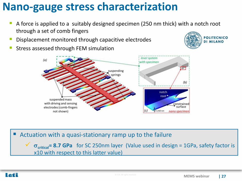
Nano-gauge stress characterization
A force is applied to a suitably designed specimen (250 nm thick) with a notch root through a set of comb fingers
Displacement monitored through capacitive electrodes
Stress assessed through FEM simulation
Actuation with a quasi-stationary ramp up to the failure
scritical= 8.7 GPa for SC 250nm layer (Value used in design = 1GPa, safety factor is x10 with respect to this latter value)
MEMS webinar | 27
© CEA. All rights reserved
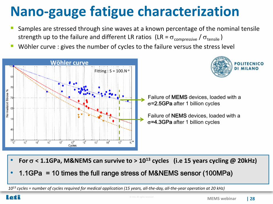
Samples are stressed through sine waves at a known percentage of the nominal tensile strength up to the failure and different LR ratios (LR = scompressive / stensile )
Wöhler curve : gives the number of cycles to the failure versus the stress level
Wöhler curveFitting : S = 100.N-a
Nano-gauge fatigue characterization
• For s < 1.1GPa, M&NEMS can survive to > 1013 cycles (i.e 15 years cycling @ 20kHz)
• 1.1GPa = 10 times the full range stress of M&NEMS sensor (100MPa)
1013 cycles = number of cycles required for medical application (15 years, all-the-day, all-the-year operation at 20 kHz)
Failure of MEMS devices, loaded with a
s=2.5GPa after 1 billion cycles
Failure of NEMS devices, loaded with a
s=4.3GPa after 1 billion cycles
MEMS webinar | 28
© CEA. All rights reserved
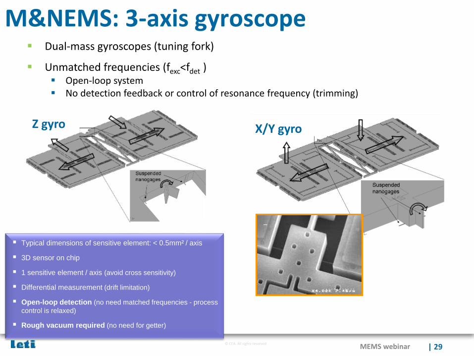
Dual-mass gyroscopes (tuning fork)
Unmatched frequencies (fexc<fdet ) Open-loop system No detection feedback or control of resonance frequency (trimming)
M&NEMS: 3-axis gyroscope
Z gyro X/Y gyro
Typical dimensions of sensitive element: < 0.5mm² / axis
3D sensor on chip
1 sensitive element / axis (avoid cross sensitivity)
Differential measurement (drift limitation)
Open-loop detection (no need matched frequencies - process
control is relaxed)
Rough vacuum required (no need for getter)
MEMS webinar | 29
© CEA. All rights reservedMEMS webinar 30
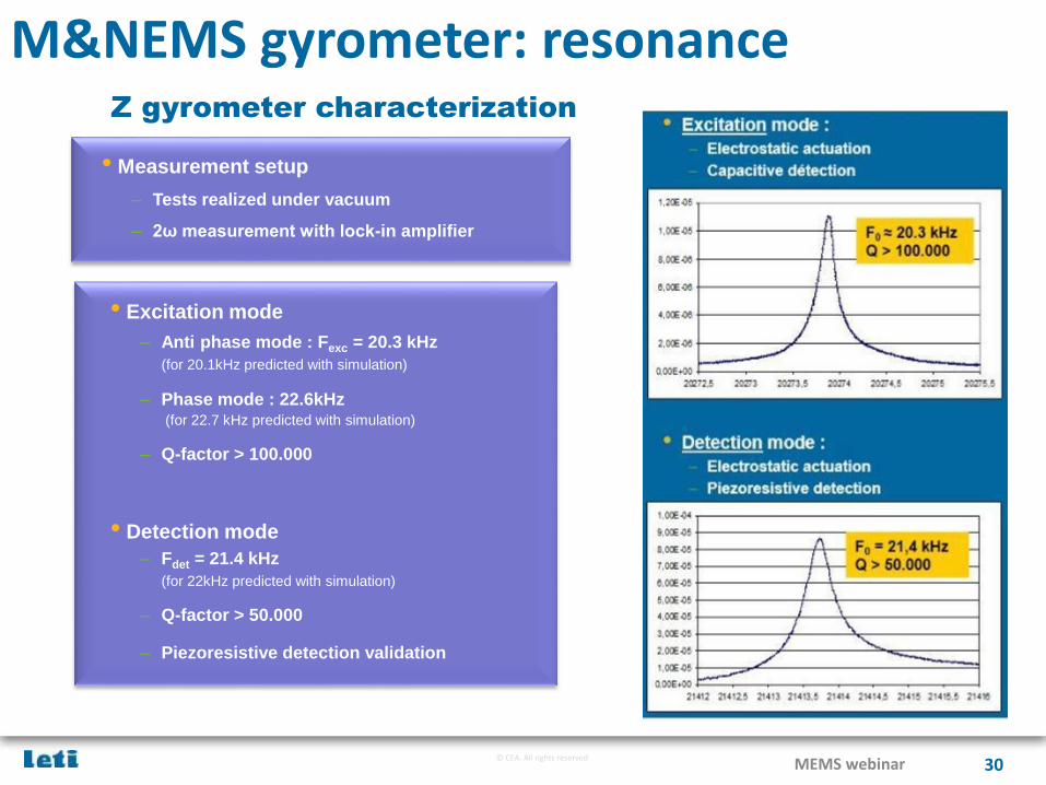
M&NEMS gyrometer: resonanceZ gyrometer characterization
• Measurement setup
– Tests realized under vacuum
– 2ω measurement with lock-in amplifier
• Excitation mode
– Anti phase mode : Fexc = 20.3 kHz
(for 20.1kHz predicted with simulation)
– Phase mode : 22.6kHz(for 22.7 kHz predicted with simulation)
– Q-factor > 100.000
• Detection mode
– Fdet = 21.4 kHz
(for 22kHz predicted with simulation)
– Q-factor > 50.000
– Piezoresistive detection validation
© CEA. All rights reservedMEMS webinar 31
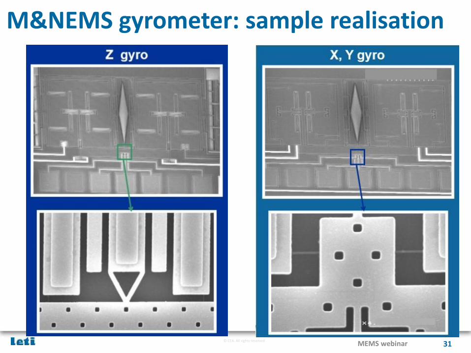
M&NEMS gyrometer: sample realisation
© CEA. All rights reservedMEMS webinar 32
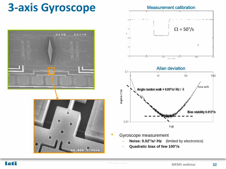
3-axis Gyroscope
• Gyroscope measurement
– Noise: 0.02°/s/√Hz (limited by electronics)
– Quadratic bias of few 100°/s
W = 50°/s
time drift
Measurement calibration
Allan deviation
© CEA. All rights reserved
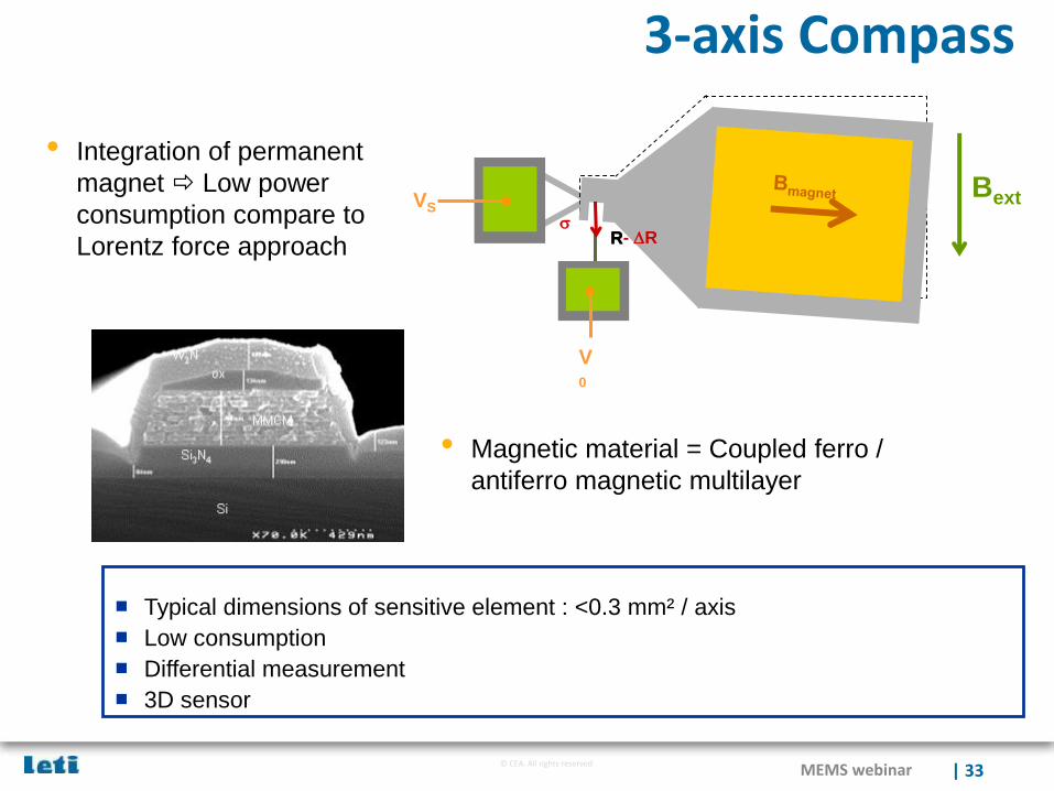
3-axis Compass
• Integration of permanent
magnet Low power
consumption compare to
Lorentz force approach
• Magnetic material = Coupled ferro /
antiferro magnetic multilayer
Typical dimensions of sensitive element : <0.3 mm² / axis
Low consumption
Differential measurement
3D sensor
Bext
s
V0
VS
RR- R
MEMS webinar | 33
© CEA. All rights reserved
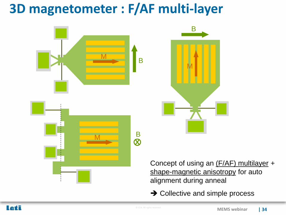
B
B
B
Concept of using an (F/AF) multilayer +
shape-magnetic anisotropy for auto
alignment during anneal
Collective and simple process
3D magnetometer : F/AF multi-layer
M
M
M
MEMS webinar | 34
© CEA. All rights reserved
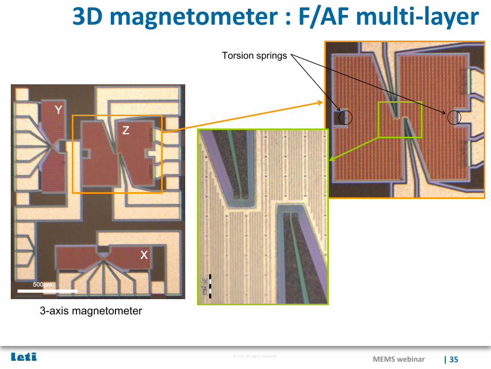
3D magnetometer : F/AF multi-layer
Y
X
Z
500µm
3-axis magnetometer
Torsion springs
MEMS webinar | 35
© CEA. All rights reservedMEMS webinar 36
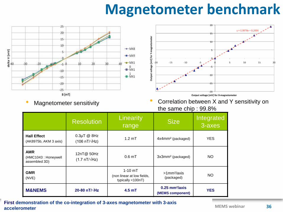
Magnetometer benchmark
ResolutionLinearity
rangeSize
Integrated
3-axes
Hall Effect
(AK8975b, AKM 3 axis)
0.3µT @ 8Hz
(106 nT/√Hz)1.2 mT 4x4mm² (packaged) YES
AMR
(HMC1043 : Honeywell
assembled 3D)
12nT@ 50Hz
(1.7 nT/√Hz)0.6 mT 3x3mm² (packaged) NO
GMR
(NVE)
1-10 mT
(non linear at low fields,
typically <100nT)
>1mm²/axis (packaged)
NO
M&NEMS 20-80 nT/√Hz 4.5 mT0.25 mm²/axis
(MEMS component)YES
• Magnetometer sensitivity • Correlation between X and Y sensitivity on
the same chip : 99.8%
First demonstration of the co-integration of 3-axes magnetometer with 3-axis
accelerometer
© CEA. All rights reservedMEMS webinar 37
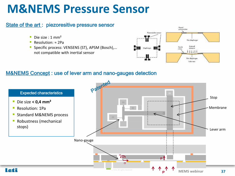
M&NEMS Pressure Sensor
M&NEMS Concept : use of lever arm and nano-gauges detection
State of the art : piezoresitive pressure sensor
Die size : 1 mm² Resolution: ≈ 2Pa Specific process: VENSENS (ST), APSM (Bosch),…
not compatible with inertial sensor
Die size < 0,4 mm²
Resolution: 1Pa
Standard M&NEMS process
Robustness (mechanical stops)
Expected characteristics
Nano-gauge
Membrane
a
Lever arm
Stop
s
F
P
© CEA. All rights reserved
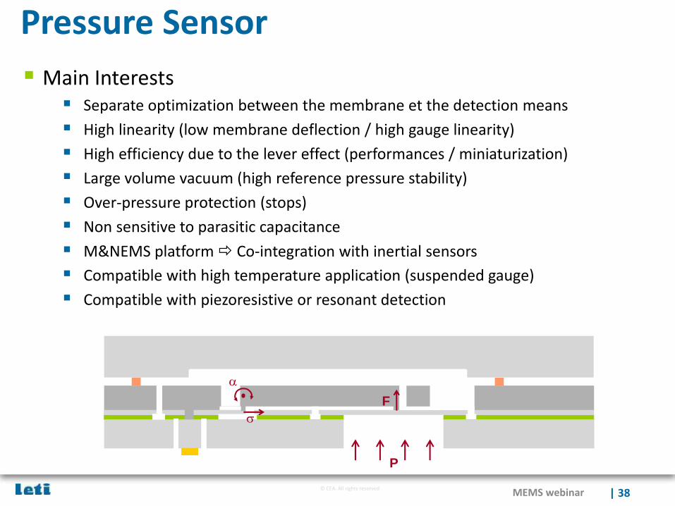
Pressure Sensor
Main Interests Separate optimization between the membrane et the detection means
High linearity (low membrane deflection / high gauge linearity)
High efficiency due to the lever effect (performances / miniaturization)
Large volume vacuum (high reference pressure stability)
Over-pressure protection (stops)
Non sensitive to parasitic capacitance
M&NEMS platform Co-integration with inertial sensors
Compatible with high temperature application (suspended gauge)
Compatible with piezoresistive or resonant detection
a
s
F
P
MEMS webinar | 38
© CEA. All rights reserved
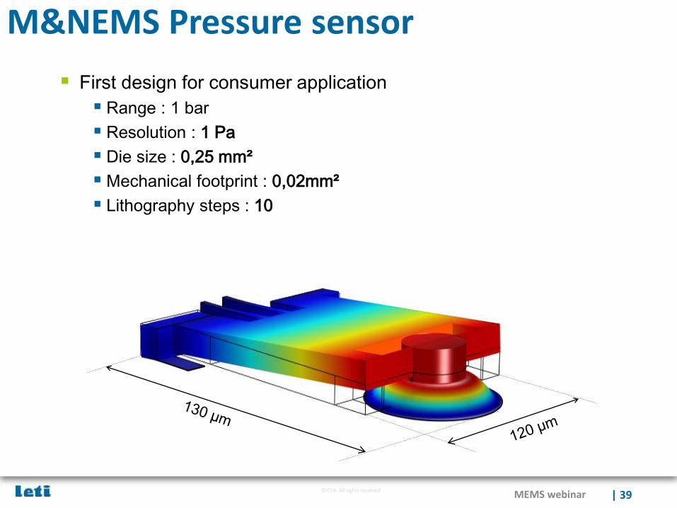
M&NEMS Pressure sensor
First design for consumer application
Range : 1 bar
Resolution : 1 Pa
Die size : 0,25 mm²
Mechanical footprint : 0,02mm²
Lithography steps : 10
MEMS webinar | 39
© CEA. All rights reserved
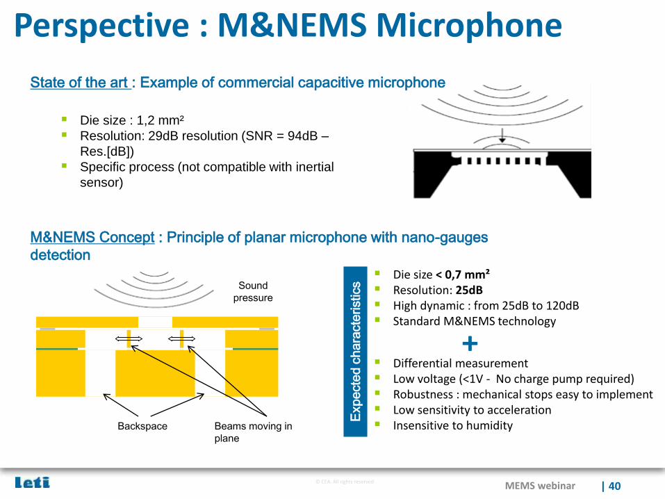
Perspective : M&NEMS Microphone
M&NEMS Concept : Principle of planar microphone with nano-gauges
detection
Backspace Beams moving in
plane
Sound
pressure
Die size < 0,7 mm² Resolution: 25dB High dynamic : from 25dB to 120dB Standard M&NEMS technology
Differential measurement Low voltage (<1V - No charge pump required) Robustness : mechanical stops easy to implement Low sensitivity to acceleration Insensitive to humidity
Die size : 1,2 mm²
Resolution: 29dB resolution (SNR = 94dB –
Res.[dB])
Specific process (not compatible with inertial
sensor)
State of the art : Example of commercial capacitive microphone
+E
xp
ecte
d c
ha
racte
ristics
MEMS webinar | 40
© CEA. All rights reserved
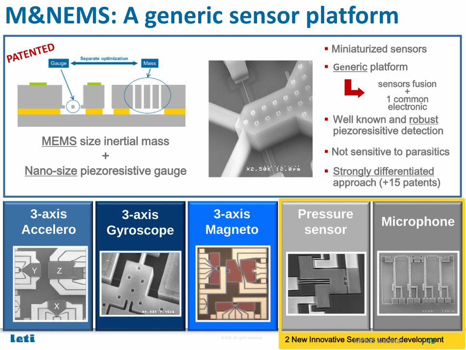
M&NEMS: A generic sensor platform Miniaturized sensors
Generic platform
sensors fusion +
1 common electronic
Not sensitive to parasiticsMEMS size inertial mass
+Nano-size piezoresistive gauge
Well known and robustpiezoresisitive detection
Strongly differentiated approach (+15 patents)
3-axis
Gyroscope
3-axis
Magneto
3-axis
Accelero
X
ZY
Pressure
sensorMicrophone
2 New Innovative Sensors under developmentMEMS webinar | 41
© CEA. All rights reserved
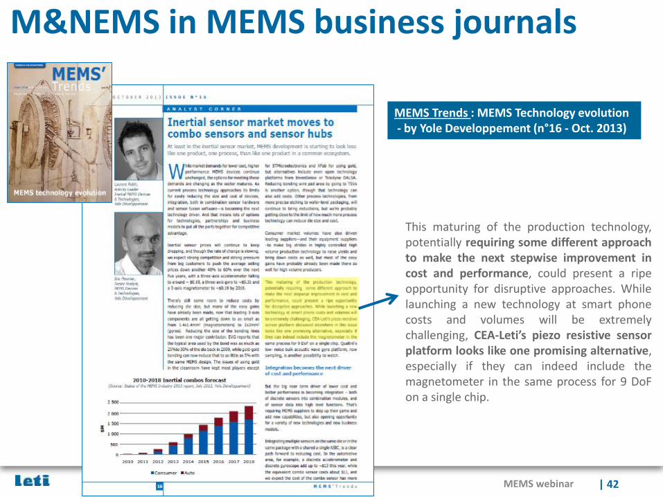
M&NEMS in MEMS business journals
MEMS Trends : MEMS Technology evolution - by Yole Developpement (n°16 - Oct. 2013)
This maturing of the production technology,potentially requiring some different approachto make the next stepwise improvement incost and performance, could present a ripeopportunity for disruptive approaches. Whilelaunching a new technology at smart phonecosts and volumes will be extremelychallenging, CEA-Leti’s piezo resistive sensorplatform looks like one promising alternative,especially if they can indeed include themagnetometer in the same process for 9 DoFon a single chip.
MEMS webinar | 42
© CEA. All rights reserved
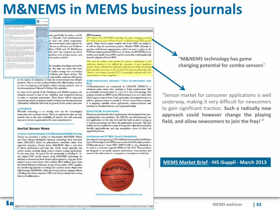
M&NEMS in MEMS business journals
“M&NEMS technology has game changing potential for combo sensors”
“Sensor market for consumer applications is wellunderway, making it very difficult for newcomersto gain significant traction. Such a radically newapproach could however change the playingfield, and allow newcomers to join the fray! ”
MEMS Market Brief - IHS iSuppli - March 2013
MEMS webinar | 43
© CEA. All rights reserved
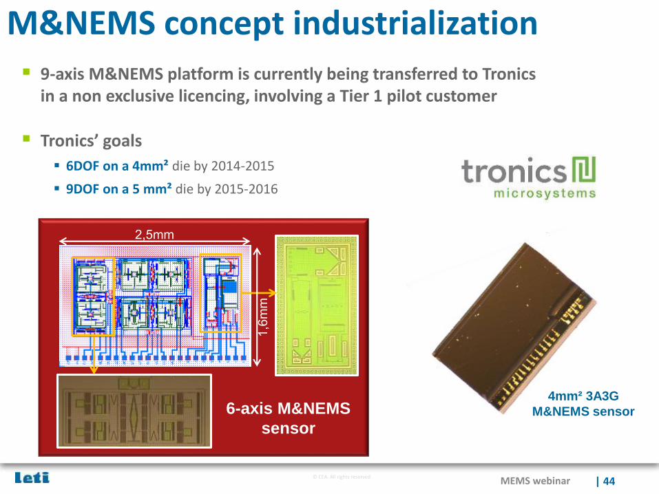
9-axis M&NEMS platform is currently being transferred to Tronicsin a non exclusive licencing, involving a Tier 1 pilot customer
Tronics’ goals
6DOF on a 4mm² die by 2014-2015
9DOF on a 5 mm² die by 2015-2016
2,5mm
1,6
mm
4mm² 3A3G
M&NEMS sensor6-axis M&NEMS
sensor
M&NEMS concept industrialization
MEMS webinar | 44
© CEA. All rights reserved
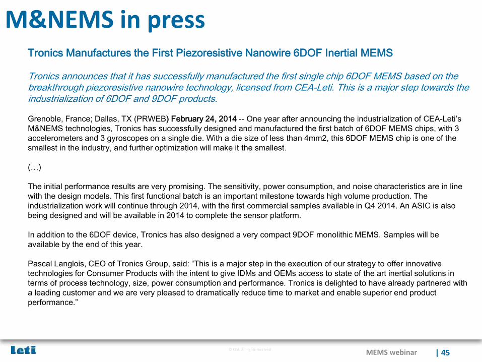
M&NEMS in pressTronics Manufactures the First Piezoresistive Nanowire 6DOF Inertial MEMS
Tronics announces that it has successfully manufactured the first single chip 6DOF MEMS based on the breakthrough piezoresistive nanowire technology, licensed from CEA-Leti. This is a major step towards the industrialization of 6DOF and 9DOF products.
Grenoble, France; Dallas, TX (PRWEB) February 24, 2014 -- One year after announcing the industrialization of CEA-Leti’s
M&NEMS technologies, Tronics has successfully designed and manufactured the first batch of 6DOF MEMS chips, with 3
accelerometers and 3 gyroscopes on a single die. With a die size of less than 4mm2, this 6DOF MEMS chip is one of the
smallest in the industry, and further optimization will make it the smallest.
(…)
The initial performance results are very promising. The sensitivity, power consumption, and noise characteristics are in line
with the design models. This first functional batch is an important milestone towards high volume production. The
industrialization work will continue through 2014, with the first commercial samples available in Q4 2014. An ASIC is also
being designed and will be available in 2014 to complete the sensor platform.
In addition to the 6DOF device, Tronics has also designed a very compact 9DOF monolithic MEMS. Samples will be
available by the end of this year.
Pascal Langlois, CEO of Tronics Group, said: “This is a major step in the execution of our strategy to offer innovative
technologies for Consumer Products with the intent to give IDMs and OEMs access to state of the art inertial solutions in
terms of process technology, size, power consumption and performance. Tronics is delighted to have already partnered with
a leading customer and we are very pleased to dramatically reduce time to market and enable superior end product
performance.”
MEMS webinar | 45
© CEA. All rights reserved
Summary
Short overview of Léti
The context of MEMS
The next steps in MEMS: Generic platforms
Physical sensors
Chemical and biological sensors
Conclusion
MEMS webinar | 46
© CEA. All rights reserved
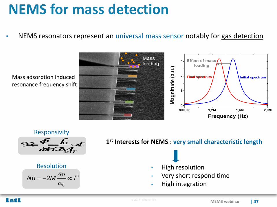
NEMS for mass detection
40
2
-=-= lM
f
m
f
eff
Responsivity
3
0
2 lMm -=
Resolution
• NEMS resonators represent an universal mass sensor notably for gas detection
Mass adsorption inducedresonance frequency shift
Mass
loading
Mass
loading
1st Interests for NEMS : very small characteristic length
• High resolution• Very short respond time• High integration
MEMS webinar | 47
© CEA. All rights reserved
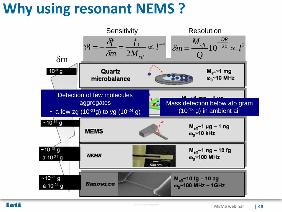
Why using resonant NEMS ?
40
2
-=-= lM
f
m
f
eff
32010 l
Q
Mm
DReff
=-
Mass detection below ato gram
(10-18 g) in ambient air
Detection of few molecules
aggregates
~ a few zg (10-21g) to yg (10-24 g)
Sensitivity Resolution
δm
MEMS webinar | 48
© CEA. All rights reserved
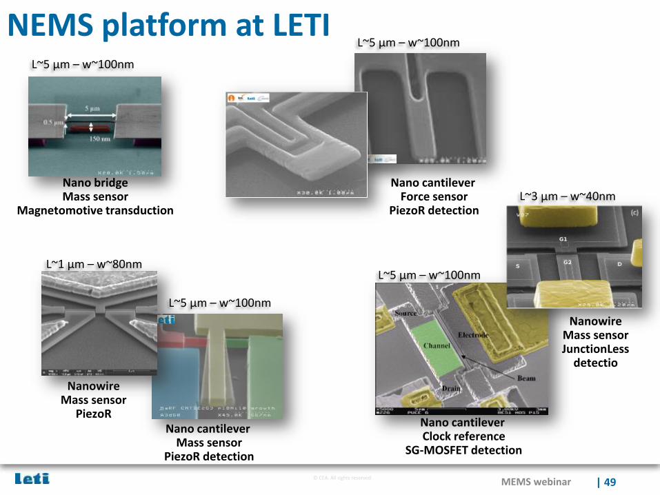
NEMS platform at LETI
| 49
Nano bridgeMass sensor
Magnetomotive transduction
L~5 µm – w~100nm
NanowireMass sensor
PiezoR
L~5 µm – w~100nm
Nano cantilever Mass sensor
PiezoR detection
L~1 µm – w~80nm
L~3 µm – w~40nm
L~5 µm – w~100nm
Nano cantilever Clock reference
SG-MOSFET detection
NanowireMass sensorJunctionLess
detectio
L~5 µm – w~100nm
Nano cantilever Force sensor
PiezoR detection
MEMS webinar
© CEA. All rights reserved
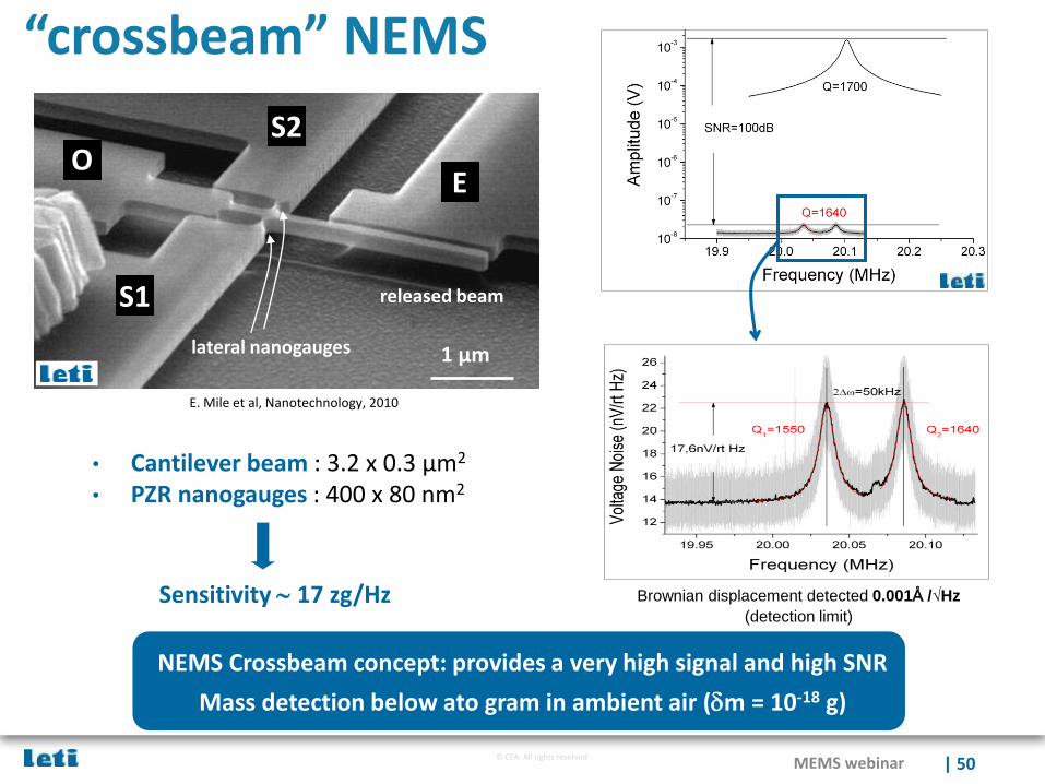
“crossbeam” NEMS
• Cantilever beam : 3.2 x 0.3 µm2
• PZR nanogauges : 400 x 80 nm2
Sensitivity 17 zg/Hz
S2
S1
EO
1 µm
released beam
lateral nanogauges
E. Mile et al, Nanotechnology, 2010
Brownian displacement detected 0.001Å /√Hz
(detection limit)
NEMS Crossbeam concept: provides a very high signal and high SNR
Mass detection below ato gram in ambient air (m = 10-18 g)
MEMS webinar | 50
© CEA. All rights reserved
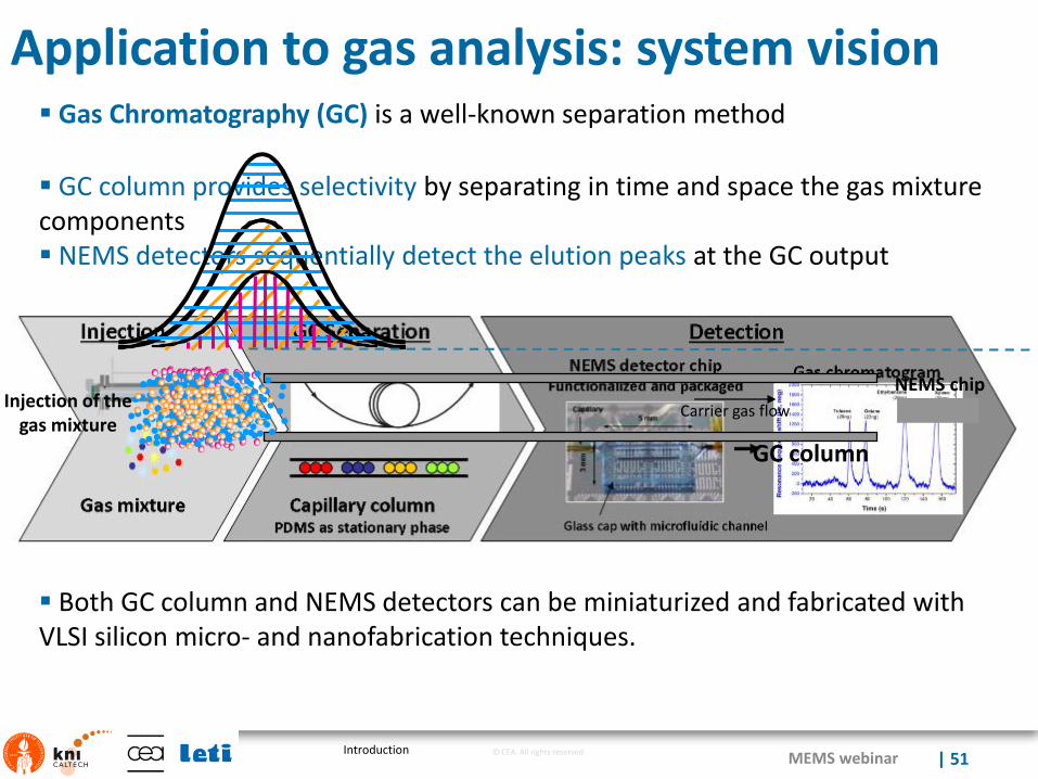
Application to gas analysis: system vision Gas Chromatography (GC) is a well-known separation method
Introduction
GC column provides selectivity by separating in time and space the gas mixture components NEMS detectors sequentially detect the elution peaks at the GC output
Both GC column and NEMS detectors can be miniaturized and fabricated with VLSI silicon micro- and nanofabrication techniques.
Injection of the gas mixture
Carrier gas flow
GC column
NEMS chip
MEMS webinar | 51
© CEA. All rights reserved
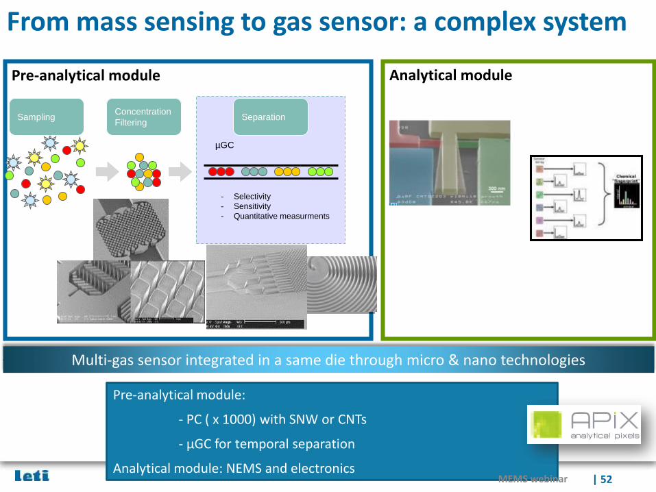
From mass sensing to gas sensor: a complex system
Pre-analytical module
SamplingConcentration
Filtering
µGC
- Selectivity
- Sensitivity
- Quantitative measurments
Separation
Multi-gas sensor integrated in a same die through micro & nano technologies
Analytical module
Detection Data treatment
Pre-analytical module:
- PC ( x 1000) with SNW or CNTs
- µGC for temporal separation
Analytical module: NEMS and electronicsMEMS webinar | 52
© CEA. All rights reserved
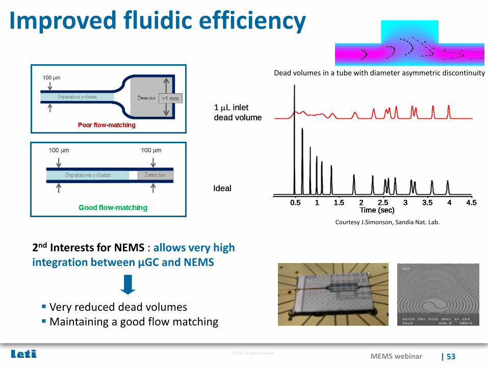
Improved fluidic efficiency
1 L inlet
dead volume
1 L inlet
dead volume
0.5 1 1.5 2 2.5 3 3.5 4 4.5 Time (sec)
Ideal
0.5 1 1.5 2 2.5 3 3.5 4 4.5 Time (sec)
0.5 1 1.5 2 2.5 3 3.5 4 4.5 Time (sec)
0.5 1 1.5 2 2.5 3 3.5 4 4.5 0.5 1 1.5 2 2.5 3 3.5 4 4.5 Time (sec)
Ideal
Dead volumes in a tube with diameter asymmetric discontinuity
Courtesy J.Simonson, Sandia Nat. Lab.
2nd Interests for NEMS : allows very high integration between µGC and NEMS
Very reduced dead volumesMaintaining a good flow matching
MEMS webinar | 53
© CEA. All rights reserved
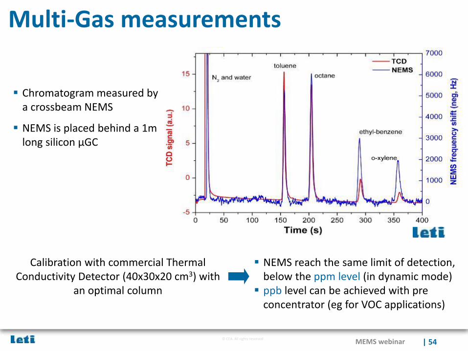
Multi-Gas measurements
Chromatogram measured by a crossbeam NEMS
NEMS is placed behind a 1m long silicon μGC
NEMS reach the same limit of detection, below the ppm level (in dynamic mode)
ppb level can be achieved with pre concentrator (eg for VOC applications)
Calibration with commercial Thermal Conductivity Detector (40x30x20 cm3) with
an optimal column
MEMS webinar | 54
© CEA. All rights reserved
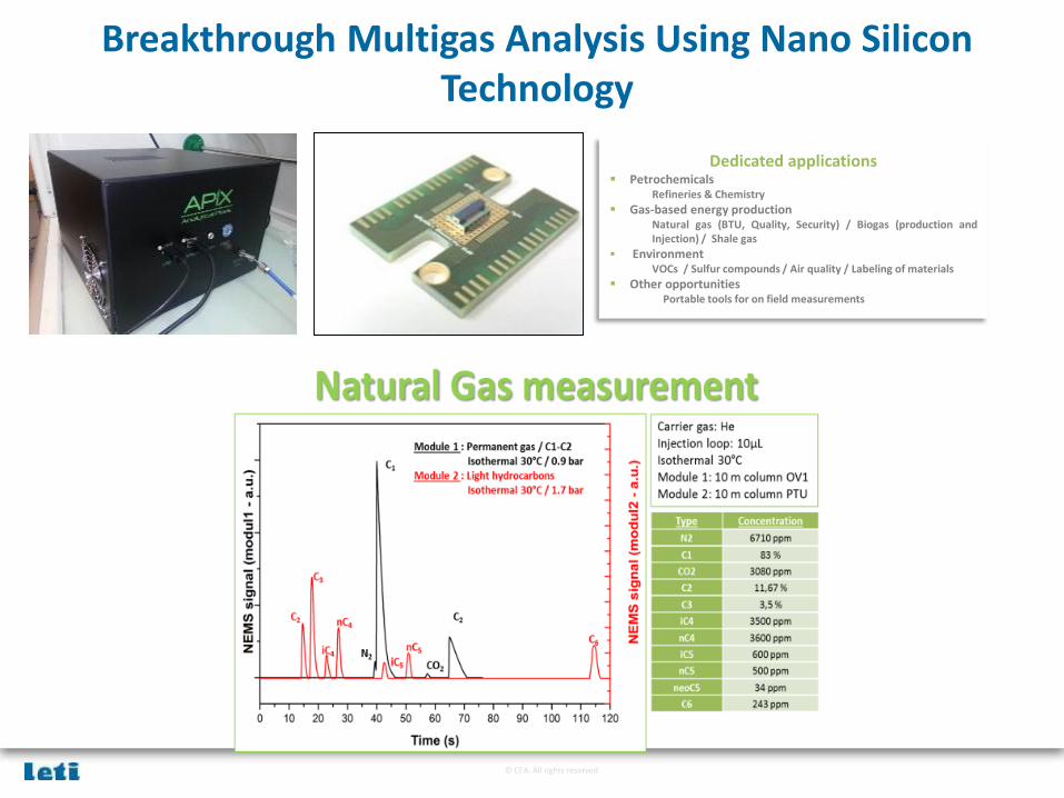
Breakthrough Multigas Analysis Using Nano Silicon Technology
Dedicated applications Petrochemicals
Refineries & Chemistry
Gas-based energy productionNatural gas (BTU, Quality, Security) / Biogas (production andInjection) / Shale gas
EnvironmentVOCs / Sulfur compounds / Air quality / Labeling of materials
Other opportunitiesPortable tools for on field measurements
© CEA. All rights reserved
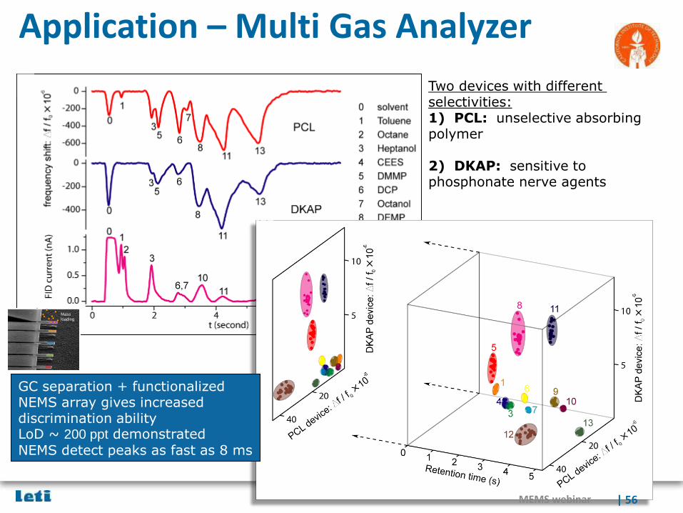
Two devices with different selectivities:1) PCL: unselective absorbingpolymer
2) DKAP: sensitive to phosphonate nerve agents
GC separation + functionalizedNEMS array gives increaseddiscrimination abilityLoD ~ 200 ppt demonstratedNEMS detect peaks as fast as 8 ms
Application – Multi Gas Analyzer
Mass
loading
MEMS webinar | 56
© CEA. All rights reserved
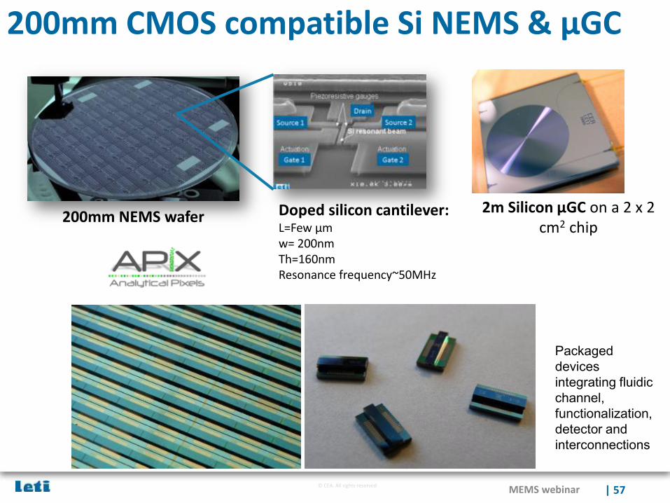
200mm NEMS wafer Doped silicon cantilever:L=Few µmw= 200nmTh=160nmResonance frequency~50MHz
200mm CMOS compatible Si NEMS & µGC
2m Silicon µGC on a 2 x 2 cm2 chip
Packaged
devices
integrating fluidic
channel,
functionalization,
detector and
interconnections
MEMS webinar | 57
© CEA. All rights reserved
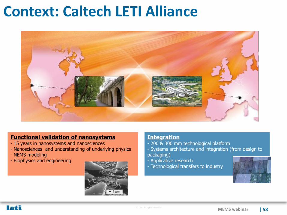
Context: Caltech LETI Alliance
Functional validation of nanosystems- 15 years in nanosystems and nanosciences- Nanosciences and understanding of underlying physics - NEMS modeling- Biophysics and engineering
Integration- 200 & 300 mm technological platform- Systems architecture and integration (from design to packaging) - Applicative research- Technological transfers to industry
MEMS webinar | 58
© CEA. All rights reserved
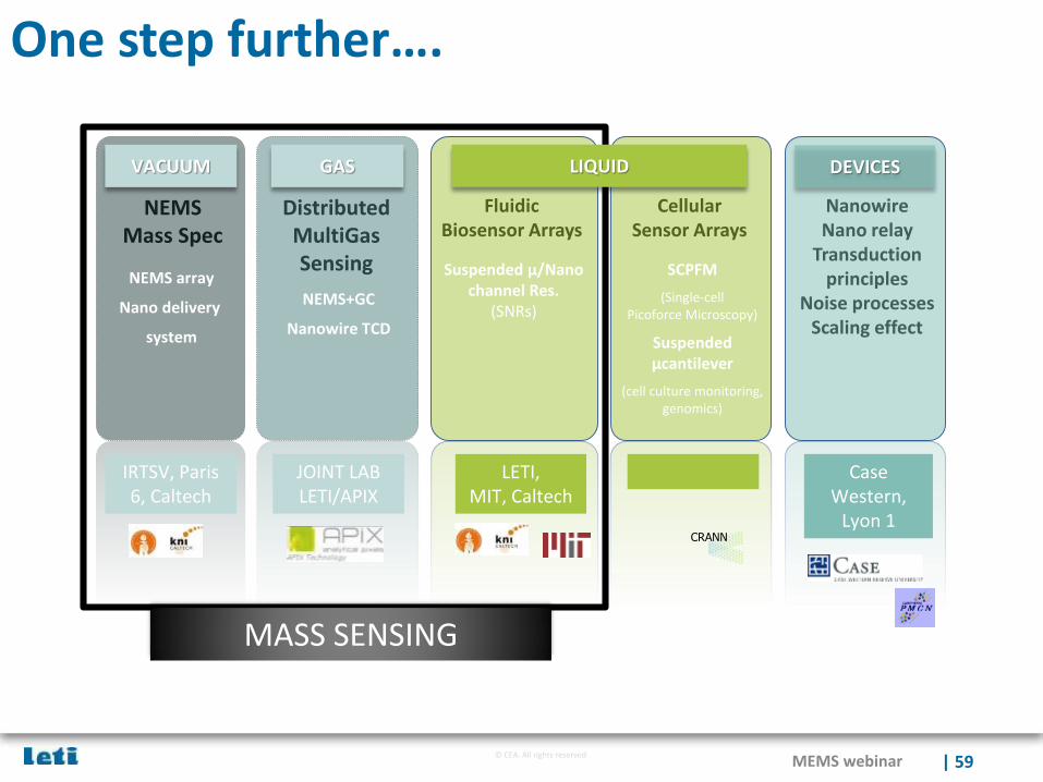
One step further….
| 59
DistributedMultiGasSensing
NEMS Mass Spec
GAS
NEMS+GC
Nanowire TCD
JOINT LABLETI/APIX
VACUUM
NEMS array
Nano delivery
system
IRTSV, Paris 6, Caltech
Fluidic Biosensor Arrays
Cellular Sensor Arrays
Suspended µ/Nano channel Res.
(SNRs)
LETI,MIT, Caltech
SCPFM
(Single-cell Picoforce Microscopy)
Suspended µcantilever
(cell culture monitoring, genomics)
LIQUID
CRANN
NanowireNano relay
Transduction principles
Noise processesScaling effect
DEVICES
Case Western,
Lyon 1
MASS SENSING
MEMS webinar
© CEA. All rights reserved
Summary
Short overview of Léti
The context of MEMS
The next steps in MEMS: Generic platforms
Physical sensors
Chemical sensors
Conclusion
MEMS webinar | 60
© CEA. All rights reserved
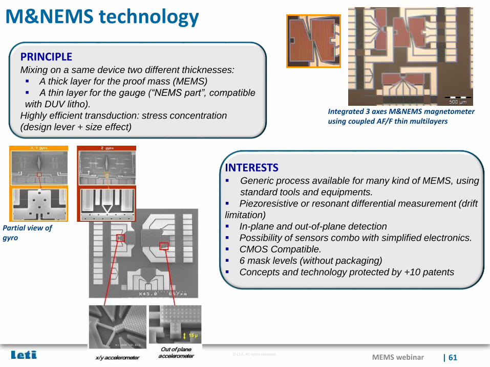
PRINCIPLEMixing on a same device two different thicknesses:
A thick layer for the proof mass (MEMS)
A thin layer for the gauge (“NEMS part”, compatible
with DUV litho).
Highly efficient transduction: stress concentration
(design lever + size effect)
INTERESTS Generic process available for many kind of MEMS, using
standard tools and equipments.
Piezoresistive or resonant differential measurement (drift
limitation)
In-plane and out-of-plane detection
Possibility of sensors combo with simplified electronics.
CMOS Compatible.
6 mask levels (without packaging)
Concepts and technology protected by +10 patents
M&NEMS technology
Integrated 3 axes M&NEMS magnetometer using coupled AF/F thin multilayers
Partial view of gyro
MEMS webinar | 61
© CEA. All rights reserved
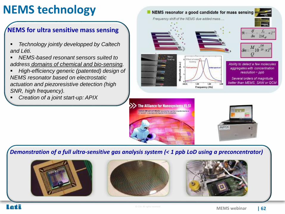
NEMS technology
Demonstration of a full ultra-sensitive gas analysis system (< 1 ppb LoD using a preconcentrator)
NEMS for ultra sensitive mass sensing
Technology jointly developped by Caltech
and Léti.
NEMS-based resonant sensors suited to
address domains of chemical and bio-sensing.
High-efficiency generic (patented) design of
NEMS resonator based on electrostatic
actuation and piezoresistive detection (high
SNR, high frequency).
Creation of a joint start-up: APIX
MEMS webinar | 62
© CEA. All rights reserved
Léti vision on MEMS
MEMS technologies are facing a maturity period. High
constraints for manufacturing simplification and cost reduction. Léti isdevelopping technologies addressing these constraints, thanks to a global approach along all the development chain.
Léti is preparing new generations of M(N)EMS.-M&NEMS is a generic technology allowing to build sensors combo.
(reasonable costs, excellent ratio perfs/die area)
-NEMS for chemical and bio chemical applications.
higher time-to-market constraints as MEMS marketsincrease. Léti is building strategic partnerships on top priority industrial
projects.
MEMS webinar | 63
© CEA. All rights reservedMEMS webinar 64
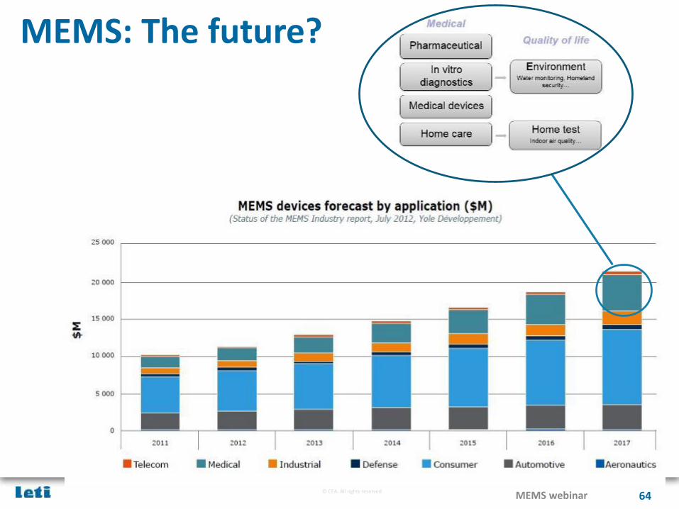
MEMS: The future?
© CEA. All rights reservedMEMS webinar | 65