Embed Size (px)
Citation preview

MEMS FOR HIGH POWER APPLICATIONS
Bruce C Kim and Rahim Kasim

Plan-view of the MEMS switch (The dimensions are approximately 300 x 1000 µm2)

Isometric-view of the MEMS switch.
Fig. Top diagram depicts the switch in the open position; the gap between the gold contact and conduction path is approximately 1 µm. Bottom diagram depicts the switch in the closed position

Fabrication (Metallization of 2X2 array)

Fabrication
Anchors
contact

Fabrication
1000 μm
100 μm
100 μm
Gap = 1.5 μm Anchor = 4.2 μm
110 μm
20 μm

Fabrication Gap = 1.5 μm Anchor = 4.2 μm

Fabrication Anchors
Nickel Bridge
Contact
conduction

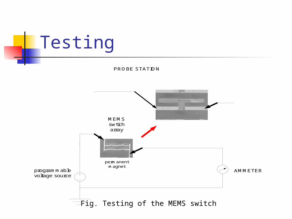
Testing
Fig. Testing of the MEMS switch
DCwith compliance
current
MEMSswtich
AMMETER
Testing
Fig. Testing of the MEMS switch
MEMSswticharray
AMMETER
permanentmagnet
programmablevoltage source
PROBE STATION

Testing – (I-V Closed)
I-V on
0
5
10
15
20
25
0 5 10 15 20 25
voltage (V)
curre
nt (m
A)
20mA compliance
10mA compliance

Testing- (I-V open) I-V (OFF)
-1.50E-10
-1.00E-10
-5.00E-11
0.00E+00
5.00E-11
1.00E-10
1.50E-10
2.00E-10
0 2 4 6 8 10 12
Voltage (V)
Cur
rent
(A
)

Conclusion
Extensive testing of 4X4 array underway (ratings and number of cycles).
Packaged array on PCB and testing.
Integration with diodes.


![[David Matthews, Kasim Dalvi] Teach Yourself Compl](https://img.pdfslide.us/doc/110x75/55cf9df4550346d033b006ff/david-matthews-kasim-dalvi-teach-yourself-compl.jpg)