Embed Size (px)
Citation preview
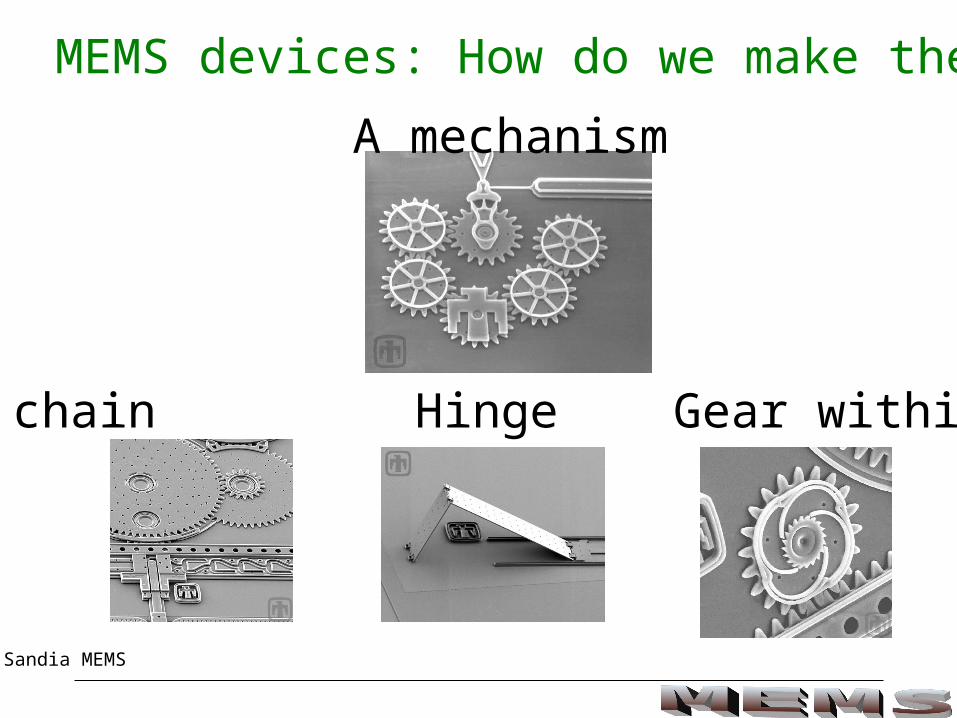
MEMS devices: How do we make them?
Sandia MEMS
Gear chain Hinge Gear within a gear
A mechanism

Basic MEMS materials Silicon and its derivatives, mostly
• Micro-electronics heritageSi is a good semiconductor, properties can be tunedSi oxide is very robustSi nitride is a good electrical insulator
Substrate Cost Metallization Machinability
Silicon High Good Very good
Plastic Low Poor Fair
Ceramic Medium Fair Poor
Glass Low Good Poor

Surface micromachining
How a cantilever is made:ht
tp:/
/ww
w.d
arpa
.mil
/mto
/mem
s

One can make devices as complex as one wishes using deposition and micromachining processes
htt
p:/
/mem
s.sa
nd
ia.g
ov/

Any MEMS device is made from the processesof deposition and removal of material
e.g. a state-of-the art MEMS electric motor
www.cronos.com
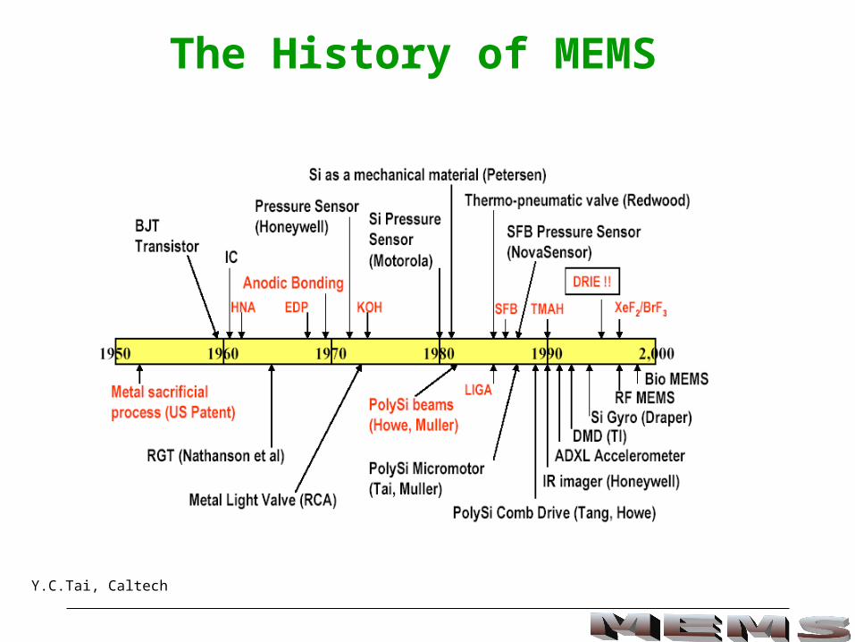
The History of MEMS
Y.C.Tai, Caltech

Bulk micromachining• Wet Chemical etching:
Bulk Si Bulk Si
Masking layer
Isotropic Anisotropic

Bulk micromachining
• Dry etching
Ions: Reactive ion etching (RIE), focused ion beams (FIB)
Laser drilling: using high powered lasers (CO2/YAG)
Electron-beam machining: sequential slow
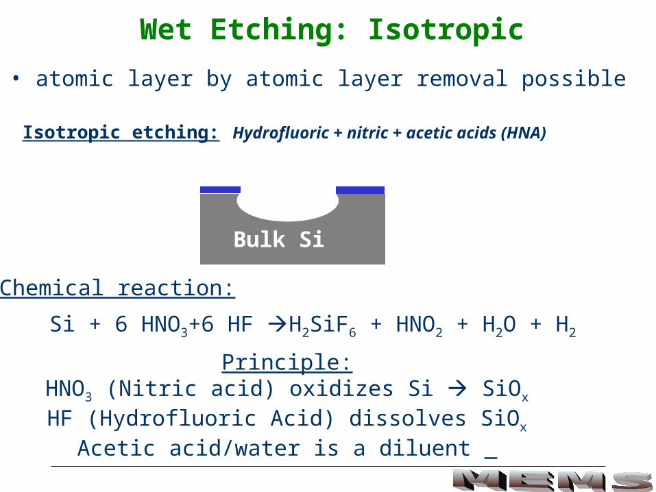
Wet Etching: Isotropic
• atomic layer by atomic layer removal possible
Isotropic etching: Hydrofluoric + nitric + acetic acids (HNA)
Bulk Si
Si + 6 HNO3+6 HF H2SiF6 + HNO2 + H2O + H2
Chemical reaction:
Principle:HNO3 (Nitric acid) oxidizes Si SiOx
HF (Hydrofluoric Acid) dissolves SiOx
Acetic acid/water is a diluent
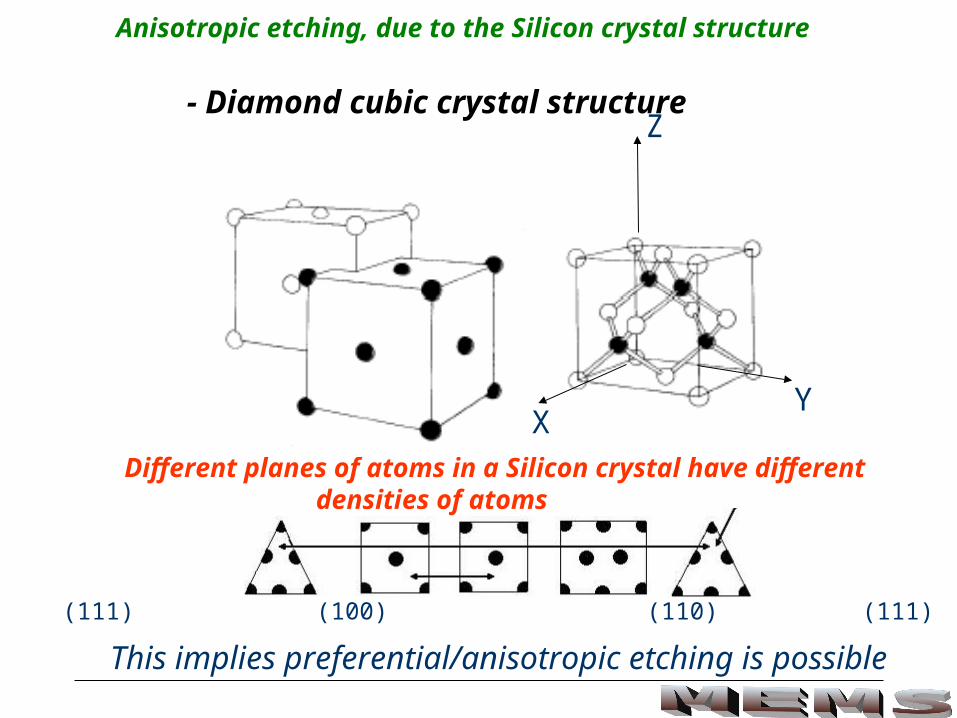
Anisotropic etching, due to the Silicon crystal structure
Different planes of atoms in a Silicon crystal have different densities of atoms
(111) (100) (110) (111)
XY
Z- Diamond cubic crystal structure
This implies preferential/anisotropic etching is possible

Applications: Anisotropic Etching
fiber
Aligning fibers Inkjet printers

Wet etching: Anisotropic Etching(100) (110)
(100) (111)
Chemical recipes:
EDP (Ethylene diamine, pyrocatechol, water)[NH2(CH2)2NH2, C6H4(OH)2]
- low SiO2 etch rate, - carcinogenic
KOH (Potassium hydroxide), - high <110> / <111> and <100>/ <111> selectivity ( ~ 500) - high SiO2 etching
TMAH (Tetra-methyl Ammonium Hydroxide: (CH3)4NOH)
- Low SiO2 and SixNy etch rate
- smaller <100> / <111> selectivity
Bulk Si Bulk Si

Comparison of wet chemical etches
Etchant Typical etching conditions
Anisotropic <100>/<111> etching ratio
Etch rate of masking layers
EDP 50-115 oC
20-80 m/hr
10-35 SiO2(2 Å/min)
SiN(1 Å/min)
KOH 50-90 oC
10-100 m/hr100-400 SiO2(2 Å/min)
SiN(1 Å/min)
TMAH 60-90 oC
10-60 m/hr10-20 SiO2(2 Å/min)
SiN(1 Å/min)
Reference: “Etch rates for Micromachining Processing” - K. R. Williams, IEEE Journal of MEMS, vol. 5, page 256, 1996.

Sensors based on (100) preferential etching
Honeywell sensor
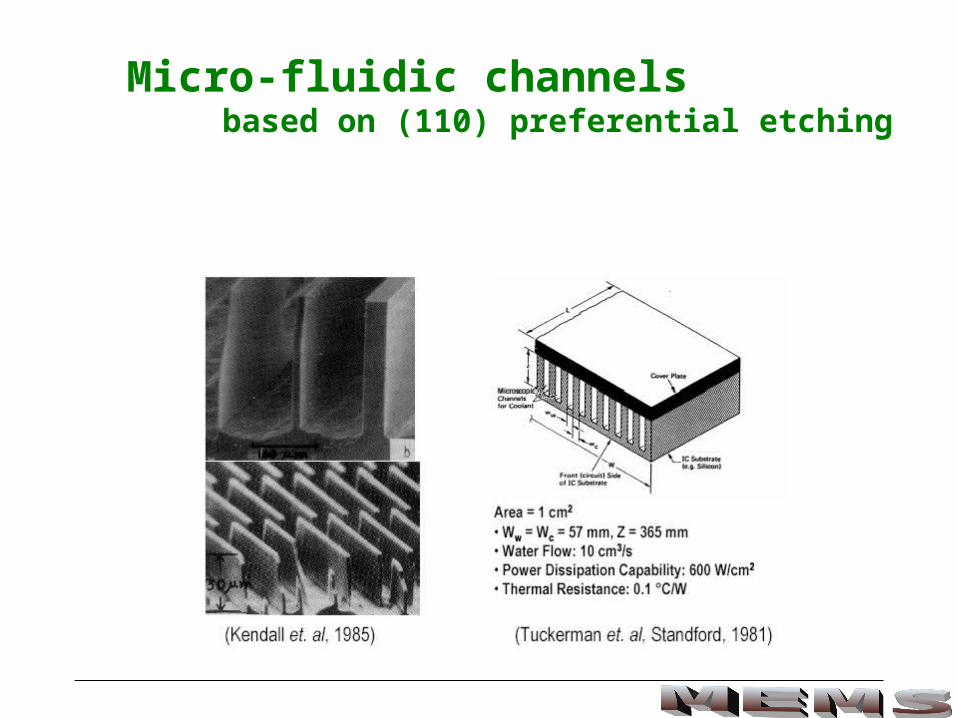
Micro-fluidic channels based on (110) preferential etching
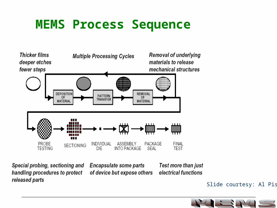
MEMS Process Sequence
Slide courtesy: Al Pisano

Surface micromachininght
tp:/
/ww
w.d
arpa
.mil
/mto
/mem
s
Sacrificial material: Silicon oxide
Structural material: polycrystalline Si (poly-Si)
Isolating material (electrical/thermal): Silicon Nitride
How a cantilever is made:

MEMS ProcessingOxidation of Silicon Silicon Oxide
(Sacrificial material)
Dry Oxidation: flowing pure oxygen over Si @ 850 – 1100 oC
(thin oxides 1- 100 nm, high quality of oxide)
Uses the Deal-Grove Model: xoxide = (BDGt)1/2
Temperature (oC) BDG m2/ hour 920 0.0049 1000 0.0117 1100 0.027

Wet Oxidation: uses steamfor thicker oxides (100nm – 1.5 mm, lower quality)
Temperature (oC) BDG (mm2/ hour)
920 0.203 1000 0.287 1100 0.510
Higher thicknesses of oxide: CVD or high pressure steam oxidation
Oxidation of Silicon Silicon Oxide (Sacrificial material)
MEMS Processing

Silicon oxide deposition
For deposition at lower temperatures, useLow Pressure Chemical Vapor Deposition (LPCVD)
SiH4 + O2 SiO2 + 2 H2 : 450 oC
Other advantages:
Can dope Silicon oxide to create PSG (phospho-silicate glass)
SiH4 + 7/2 O2 + 2 PH3 SiO2:P + 5 H2O : 700 oC
PSG: higher etch rate, flows easier (better topography)
SiH4 + O2
425-450 oC0.2-0.4 Torr
LTO: Low Temperature Oxidation process

Case study: Poly-silicon growth
- by Low Pressure Chemical Vapor Deposition- T: 580-650 oC, P: 0.1-0.4 Torr
Effect of temperature
Amorphous Crystalline: 570 oCEqui-axed grains: 600 oCColumnar grains: 625 oC
(110) crystal orientation: 600 – 650 oC (100) crystal orientation: 650 – 700 oC
SiH4
Amorphous film570 oC
Crystalline film620 oC
Kam
ins,T
. 1998 Poly-S
i for ICs an
d d
iplays, 1998

Poly-silicon growthTemperature has to be very accurately controlledas grains grow with temperature, increasing surface roughness, causing loss of pattern resolution and stresses in MEMS
Mechanisms of grain growth:
1. Strain induced growth- Minimize strain energy due to mechanical deformation, doping … - Grain growth time
2. Grain boundary growth- To reduce surface energy (and grain boundary area)- Grain growth (time)1/2
3. Impurity drag- Can accelerate/prevent grain boundary movement- Grain growth (time)1/3

Grains control properties• Mechanical properties Stress state: Residual compressive stress (500 MPa)
- Amorphous/columnar grained structures: Compressive stress- Equiaxed grained structures: Tensile stress- Thick films have less stress than thinner films
-ANNEALING CAN REDUCE STRESSES BY A FACTOR OF 10-100
•Thermal and electrical properties Grain boundaries are a barrier for electrons
e.g. thermal conductivity could be 5-10 times lower (0.2 W/cm-K)
• Optical properties Rough surfaces!
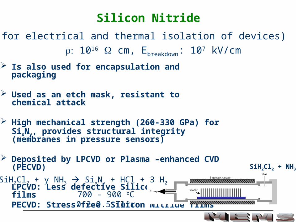
Silicon Nitride
Is also used for encapsulation and packaging
Used as an etch mask, resistant to chemical attack
High mechanical strength (260-330 GPa) for SixNy, provides structural integrity (membranes in pressure sensors)
Deposited by LPCVD or Plasma –enhanced CVD (PECVD)
LPCVD: Less defective Silicon Nitride filmsPECVD: Stress-free Silicon Nitride films
(for electrical and thermal isolation of devices)
1016 cm, Ebreakdown: 107 kV/cm
SiH2Cl2 + NH3
x SiH2Cl2 + y NH3 SixNy + HCl + 3 H2
700 - 900 oC0.2-0.5 Torr
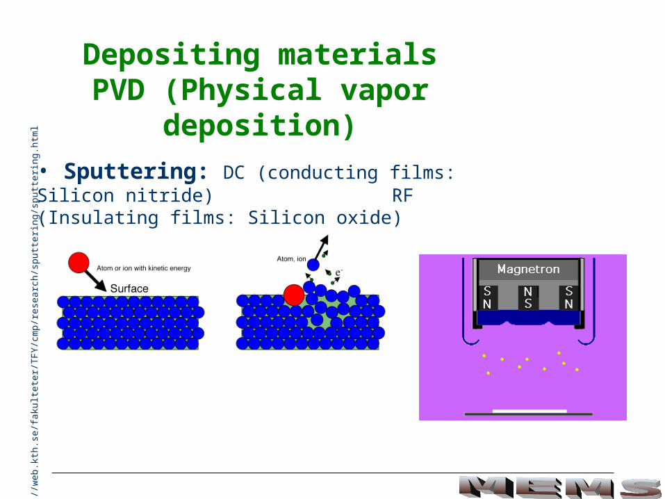
Depositing materialsPVD (Physical vapor deposition)
• Sputtering: DC (conducting films: Silicon nitride) RF (Insulating films: Silicon oxide)
http
://w
eb.k
th.s
e/fa
kulte
ter/
TFY
/cm
p/re
sear
ch/s
putte
ring
/spu
tteri
ng.h
tml

Depositing materialsPVD (Physical vapor deposition)
• Evaporation (electron-beam/thermal)
Commercial electron-beam evaporator (ITL, UCSD)
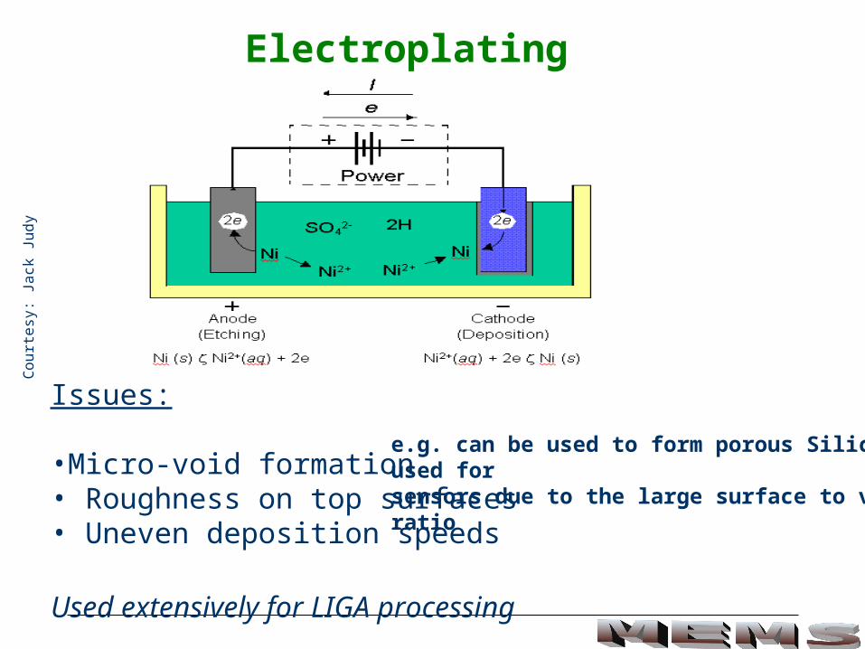
Electroplating
e.g. can be used to form porous Silicon, used for sensors due to the large surface to volume ratio
Cou
rtes
y: J
ack
Judy
Issues: •Micro-void formation• Roughness on top surfaces• Uneven deposition speeds
Used extensively for LIGA processing

Depositing materials –contd.-
• Spin-on (sol-gel)
e.g. Spin-on-Glass (SOG) used as a sacrificial molding material, processing can be done at low temperatures
Si wafer
Dropper
Surface micromachining- Technique and issues- Dry etching (DRIE)
Other MEMS fabrication techniques- Micro-molding- LIGA
Other materials in MEMS- SiC, diamond, piezo-electrics,magnetic materials, shape memory alloys …
MEMS foundry processes- How to make a micro-motor
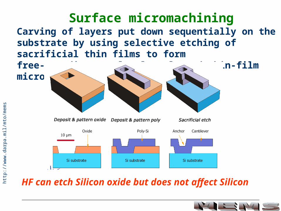
Surface micromachiningCarving of layers put down sequentially on the substrate by using selective etching of sacrificial thin films to form free-standing/completely released thin-film microstructures
http
://w
ww
.dar
pa.m
il/m
to/m
ems
HF can etch Silicon oxide but does not affect Silicon
Release step

Release of MEMS structures A difficult step, due to surface tension forces:
Surface Tension forces are greater than gravitational forces ( L) ( L)3

Release of MEMS structures To overcome this problem:
(1) Use of alcohols/ethers, which sublimate, at release step
(2) Surface texturing
(3) Supercritical CO2 drying: avoids the liquid phase
35oC, 1100 psi
Si substrate
Cantilever
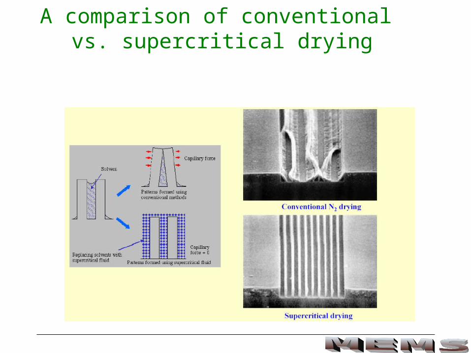
A comparison of conventional vs. supercritical drying

Reactive Ion Etching (RIE) DRY plasma based etching
Deep RIE (DRIE): • Excellent selectivity to mask material (30:1)• Moderate etch rate (1-10 m/minute)• High aspect ratio (10:1), large etch depths possible
http
://w
ww
.mem
sgui
de.c
om

Deep Reactive Ion Etching (DRIE)
Bosch Process Alternate etching (SF6) +Passivation (C4F8)
• Bowing: bottom is wider• Lag: uneven formation
A side effect of a glow discharge polymeric species created
Plasma processes: Deposition of polymeric material from plasma vs. removal of material
Usual etching processes result in a V-shaped profile

Gas phase Silicon etching
XeF2 BrF3
Developed at IBM (1962) Developed at Bell labs (1984)
2 XeF2 + Si 2 Xe + SiF4 4 BrF3 + 3 Si 2 Br2 + 3 SiF4
Cost: $150 to etch 1 g of Si $16 for 1 g of Si
• Room temperature process• No surface tension forces• No charging effects• Isotropic
Etching rate: 1-10 m/minute

Micro-molding C
. Kel
ler
et a
l, So
lid s
tate
sen
sor
& a
ctua
tor
wor
ksho
p, 1
994
-For thick films (> 100 m)
- HEXSIL/PDMS, compatible with Bio-MEMS
- loss of feature definition after repeated replication
- Thermal and mechanical stability

LIGA (LIthographie, Galvanoformung, Abformung)
For high aspect ratio structures
• Thick resists (> 1 mm)• high –energy x-ray lithography ( > 1 GeV)
Millimeter/sub-mm sized objects which require precision
Mass spectrometer with hyperbolic armsElectromagnetic motor

Capability Bulk Surface LIGA
Max. structural thickness Wafer thickness < 50 m 500 m
Planar geometry Rectangular Unrestricted Unrestricted
Min. planar feature size 2 depth < 1 m < 3 m
Side-wall features 54.7o slope Limited by dry etch 0.2 m
Surface & edge
definitions
Excellent Adequate Very good
Material properties Very well controlled
Adequate Well controlled
Integration with electronics
Demonstrated Demonstrated Difficult
Capital Investment Low Moderate High
Published knowledge Very high High Moderate
Technology Comparison
Bulk vs. Surface micromachining vs. LIGA