Embed Size (px)
Citation preview
MEMS
Class 5
Micromachining Technologies
Mohammad Kilani
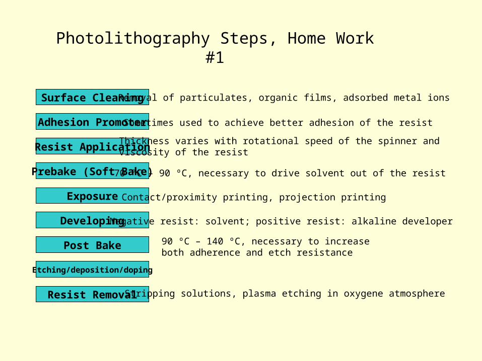
Photolithography Steps, Home Work #1
Surface Cleaning
Adhesion Promoter
Resist Application
Prebake (Soft Bake)
Exposure
Developing
Post Bake
Etching/deposition/doping
Removal of particulates, organic films, adsorbed metal ions
Sometimes used to achieve better adhesion of the resist
Thickness varies with rotational speed of the spinner andviscosity of the resist
70 °C – 90 ºC, necessary to drive solvent out of the resist
Contact/proximity printing, projection printing
Negative resist: solvent; positive resist: alkaline developer
90 ºC – 140 ºC, necessary to increase both adherence and etch resistance
Resist Removal Stripping solutions, plasma etching in oxygene atmosphere

Surface Cleaning
• Why is it important?
• How is it done?
• Physics/chemistry?
• Parameters affecting it?
Report + 10 min. PowerPoint presentation
Micromachining Technologies
• Lithographic Technologies:• Bulk Micromachining• Surface Micromachining• LIGA
• Nonlithographic Technologies:• Ultraprecision Mechanical Machining• Laser Machining• Electrodischarge Machining• Screen Printing• Microcontact Printing• Nanoimprint Lithography• Hot Embossing• Ultrasonic Machining
Bulk Micromachining
• Realize micromechanical structures within the bulk of a single-crystal silicon wafer by selectively removing (‘etching’) wafer material.
• Significant amounts of silicon are removed from a substrate to form membranes and a variety of trenches, holes, or other structures.
• It emerged in the early 1960s and has been used since then in the fabrication of different microstructures.
• It is utilized in the manufacturing of the majority of commercial devices – almost all pressure sensors and silicon valves and 90% of silicon accelerometers.
• The microstructures fabricated may cover the thickness range from submicron to full wafer thickness (200 to 500 µm) and the lateral size range from submicron to the lateral dimensions of a full wafer.
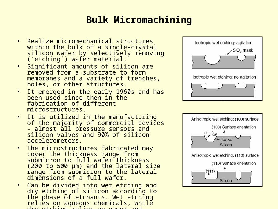
• Can be divided into wet etching and dry etching of silicon according to the phase of etchants. Wet etching relies on aqueous chemicals, while dry etching relies on vapor and plasma etchants.
• Wafer-bonding is often necessary for the assembled MEMS devices.
Bulk Micromachining – Wet Etching
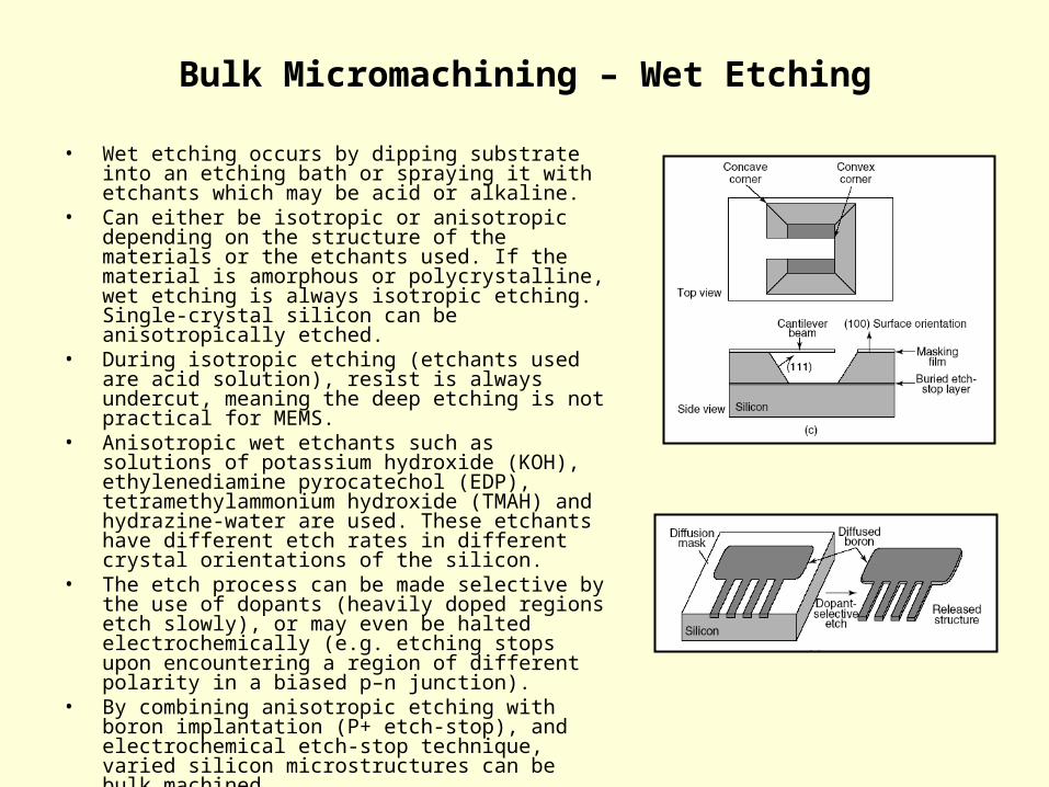
• Wet etching occurs by dipping substrate into an etching bath or spraying it with etchants which may be acid or alkaline.
• Can either be isotropic or anisotropic depending on the structure of the materials or the etchants used. If the material is amorphous or polycrystalline, wet etching is always isotropic etching. Single-crystal silicon can be anisotropically etched.
• During isotropic etching (etchants used are acid solution), resist is always undercut, meaning the deep etching is not practical for MEMS.
• Anisotropic wet etchants such as solutions of potassium hydroxide (KOH), ethylenediamine pyrocatechol (EDP), tetramethylammonium hydroxide (TMAH) and hydrazine-water are used. These etchants have different etch rates in different crystal orientations of the silicon.
• The etch process can be made selective by the use of dopants (heavily doped regions etch slowly), or may even be halted electrochemically (e.g. etching stops upon encountering a region of different polarity in a biased p–n junction).
• By combining anisotropic etching with boron implantation (P+ etch-stop), and electrochemical etch-stop technique, varied silicon microstructures can be bulk machined
Bulk Micromachining – Dry Etching
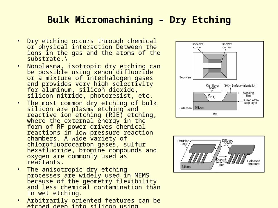
• Dry etching occurs through chemical or physical interaction between the ions in the gas and the atoms of the substrate.\
• Nonplasma, isotropic dry etching can be possible using xenon difluoride or a mixture of interhalogen gases and provides very high selectivity for aluminum, silicon dioxide, silicon nitride, photoresist, etc.
• The most common dry etching of bulk silicon are plasma etching and reactive ion etching (RIE) etching, where the external energy in the form of RF power drives chemical reactions in low-pressure reaction chambers. A wide variety of chlorofluorocarbon gases, sulfur hexafluoride, bromine compounds and oxygen are commonly used as reactants.
• The anisotropic dry etching processes are widely used in MEMS because of the geometry flexibility and less chemical contamination than in wet etching.
• Arbitrarily oriented features can be etched deep into silicon using anisotropic dry etching. Very deep silicon microstructures can be obtained by the deep RIE (DRIE) dry etching
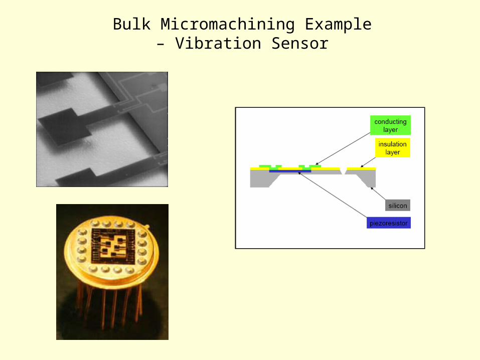
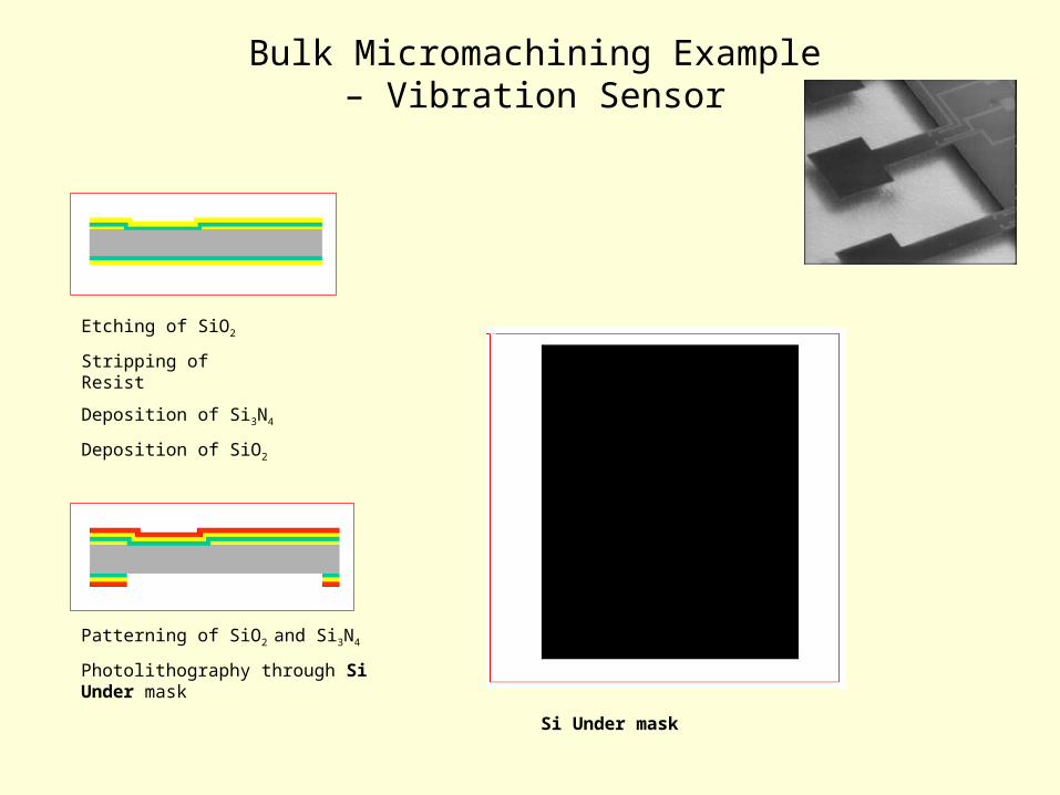
Bulk Micromachining Example – Vibration Sensor
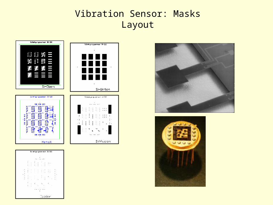
Vibration Sensor: Masks Layout
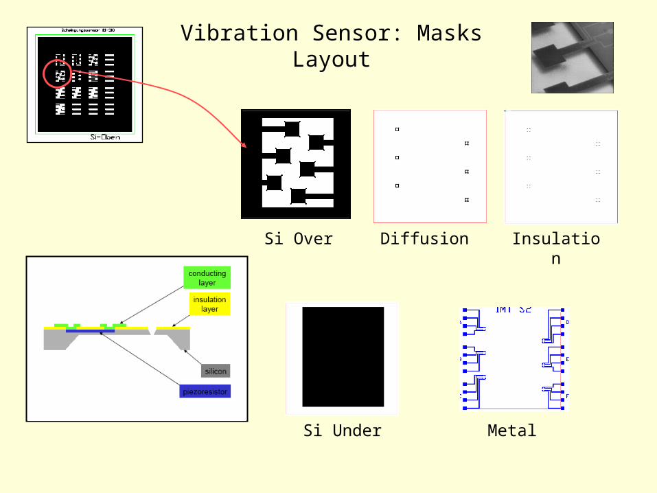
Vibration Sensor: Masks Layout
Diffusion InsulationSi Over
Si Under Metal
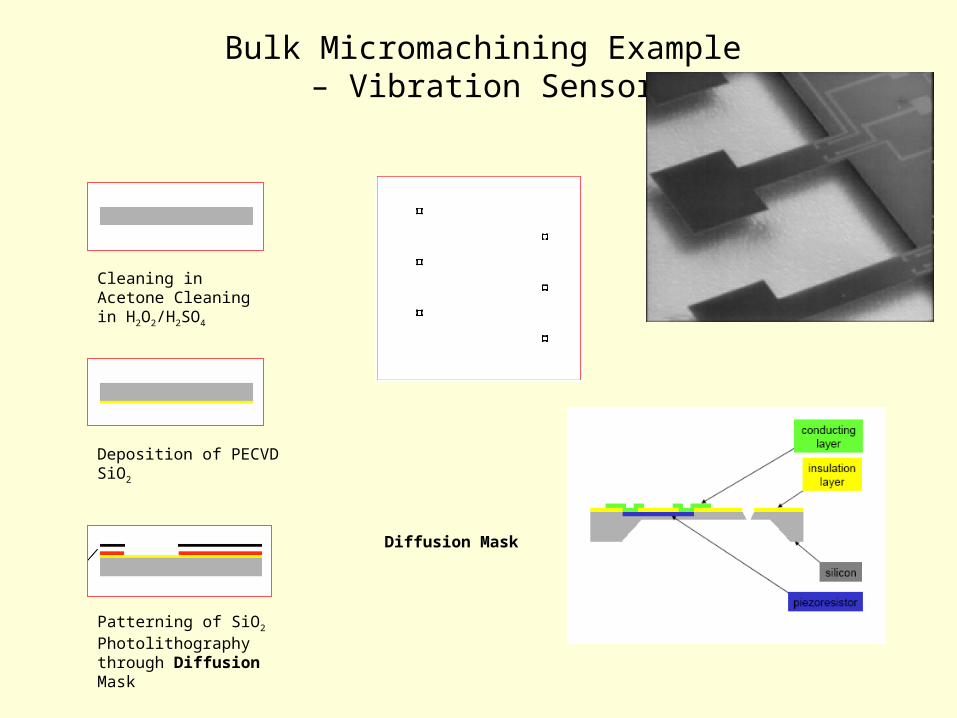
Bulk Micromachining Example – Vibration Sensor
Cleaning in Acetone Cleaning in H2O2/H2SO4
Deposition of PECVD SiO2
Patterning of SiO2 Photolithography through Diffusion Mask
Diffusion Mask
Bulk Micromachining Example – Vibration Sensor
Etching of SiO2
Stripping of Resist
Deposition of Si3N4
Deposition of SiO2
Patterning of SiO2 and Si3N4
Photolithography through Si Under mask
Si Under mask
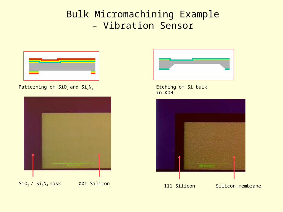
Bulk Micromachining Example – Vibration Sensor
Etching of Si bulk in KOHPatterning of SiO2 and Si3N4
SiO2 / Si3N4 mask 001 Silicon 111 Silicon Silicon membrane
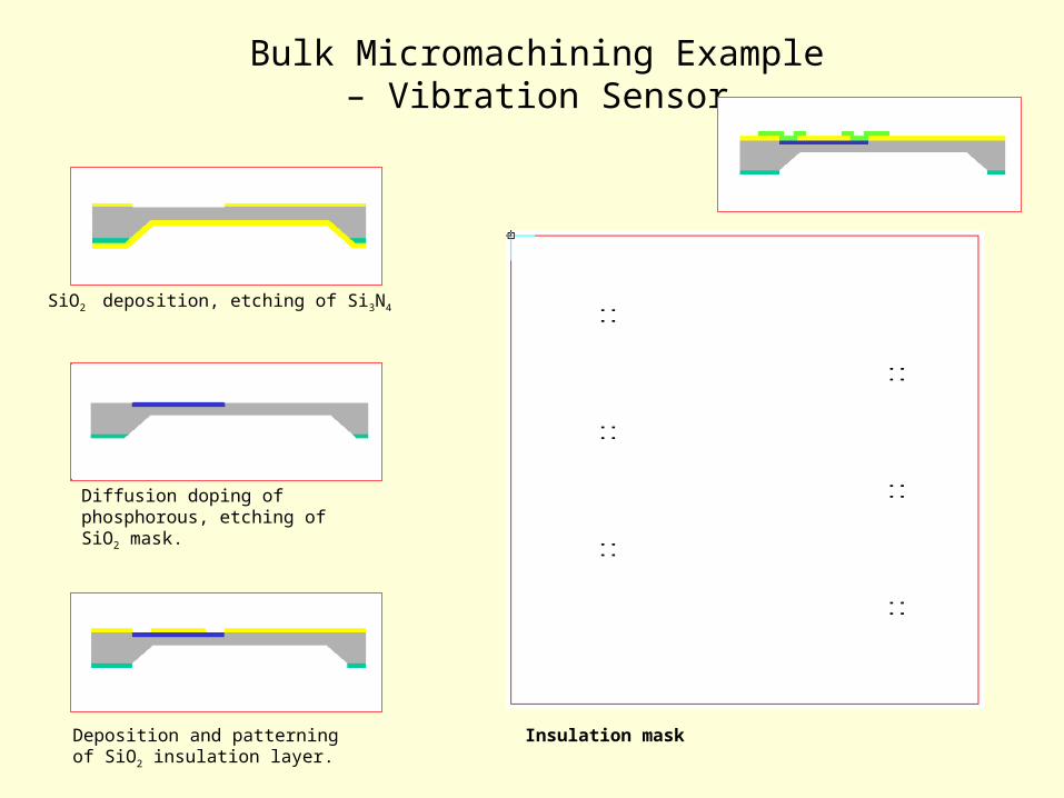
Bulk Micromachining Example – Vibration Sensor
SiO2 deposition, etching of Si3N4
Diffusion doping of phosphorous, etching of SiO2 mask.
Deposition and patterning of SiO2 insulation layer.
Insulation mask
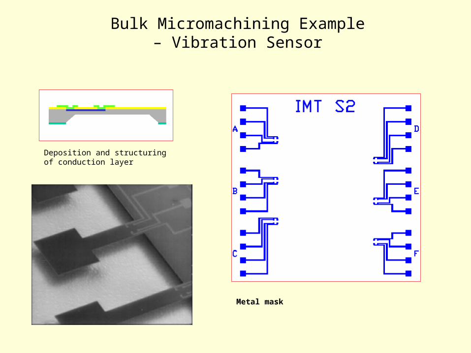
Bulk Micromachining Example – Vibration Sensor
Deposition and structuring of conduction layer
Metal mask
Bulk Micromachining Example – Vibration Sensor
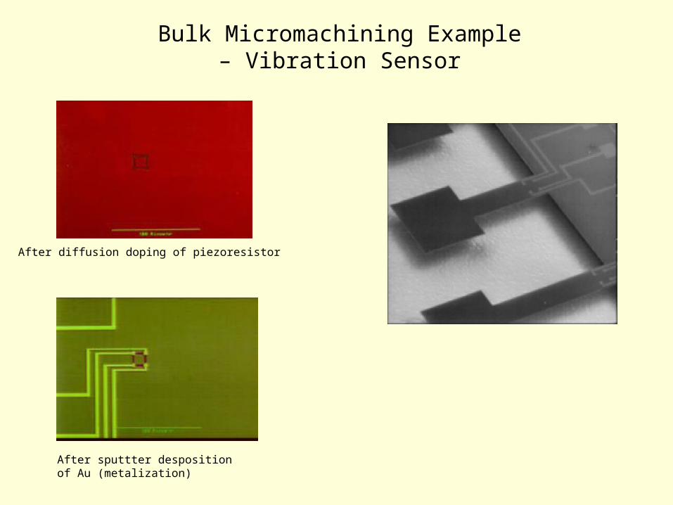
After diffusion doping of piezoresistor
After sputtter desposition of Au (metalization)
Bulk Micromachining Example – Vibration Sensor
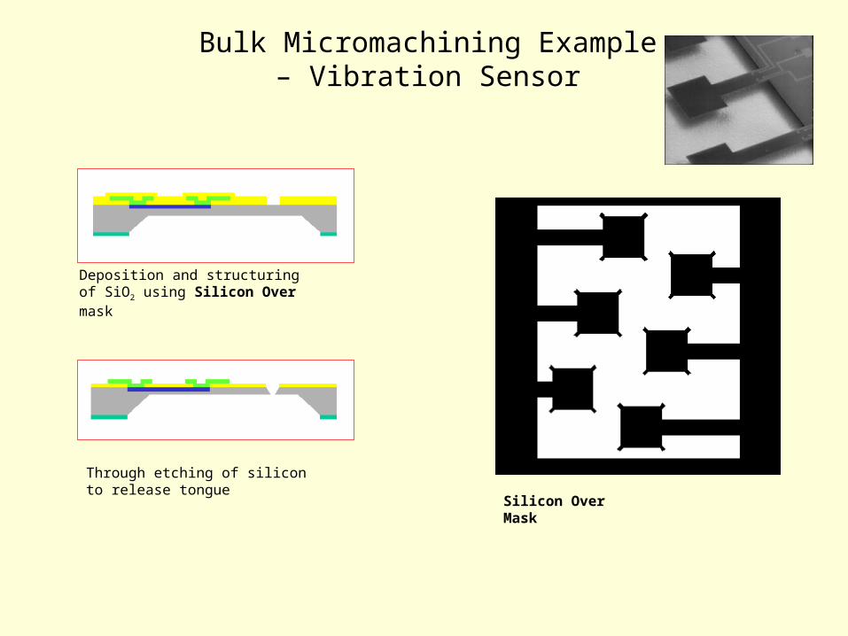
Deposition and structuring of SiO2 using Silicon Over mask
Silicon Over Mask
Through etching of silicon to release tongue
Bulk Micromachining Example – Vibration Sensor
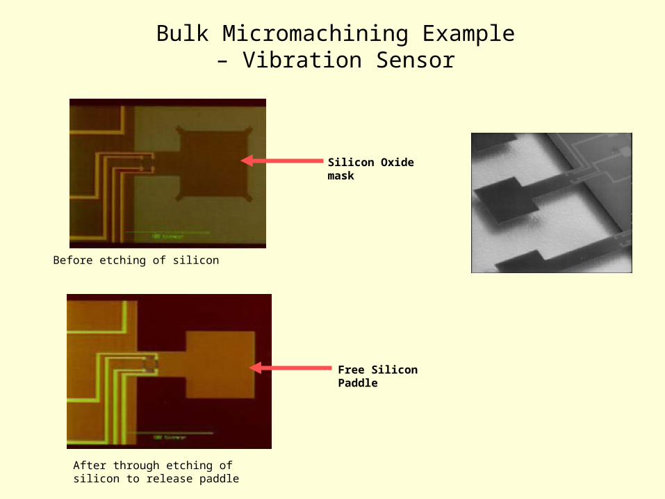
Silicon Oxide mask
Free Silicon Paddle
Before etching of silicon
After through etching of silicon to release paddle
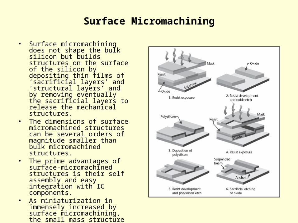
Surface Micromachining
• Surface micromachining does not shape the bulk silicon but builds structures on the surface of the silicon by depositing thin films of ‘sacrificial layers’ and ‘structural layers’ and by removing eventually the sacrificial layers to release the mechanical structures.
• The dimensions of surface micromachined structures can be several orders of magnitude smaller than bulk micromachined structures.
• The prime advantages of surface-micromachined structures is their self assembly and easy integration with IC components.
• As miniaturization in immensely increased by surface micromachining, the small mass structure involved may be insufficient for a number of mechanical sensing and actuation applications.
Surface Micromachining
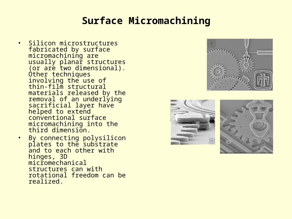
• Silicon microstructures fabricated by surface micromachining are usually planar structures (or are two dimensional). Other techniques involving the use of thin-film structural materials released by the removal of an underlying sacrificial layer have helped to extend conventional surface micromachining into the third dimension.
• By connecting polysilicon plates to the substrate and to each other with hinges, 3D micromechanical structures can with rotational freedom can be realized.
Surface Micromachining
• Surface micromachining requires a compatible set of structural materials, sacrificial materials and chemical etchants.
• The structural materials must possess satisfactory mechanical properties; e.g. high yield and fracture stresses, minimal creep and fatigue and good wear resistance.
• The sacrificial materials must have good mechanical properties to avoid device failure during fabrication. These properties include good adhesion and low residual stresses in order to eliminate device failure by delamination and/or cracking.
• The etchants to remove the sacrificial materials must have excellent etch selectivity and they must be able to etch off the sacrificial materials without affecting the structural ones. In addition the etchants must have proper viscosity and surface tension characteristics.
Surface Micromachining – Compatible Sets
Polysilicon-Silicon dioxide-HF:LPCVD polysilicon as the structural material and LPCVD oxide as the sacrificial material. The oxide is readily dissolved in HF solution without the polysilicon being affected. Together with this material system, silicon nitride is often used for electrical insulation. This is the common IC compatible materials used in surface micromachining e,g. MUMPS and SUMMiT.
Polyimide-aluminum- Acid-based etchants; Polyimide is the structural material and aluminum is the sacrificial material. Acid-based etchants are used to dissolve the aluminum sacrificial layer.
Silicon nitride-polysilicon- KOH and EDP; Silicon nitride is used as the structural material, whereas polysilicon is the sacrificial material. For this material system, silicon anisotropic etchants such as KOH and EDP are used to dissolve polysilicon.
Tungsten-silicon dioxide- HF:CVD deposited tungsten is used as the structural material with oxide as the sacrificial material. HF solution is used to remove the sacrificial oxide.
Surface Micromachining
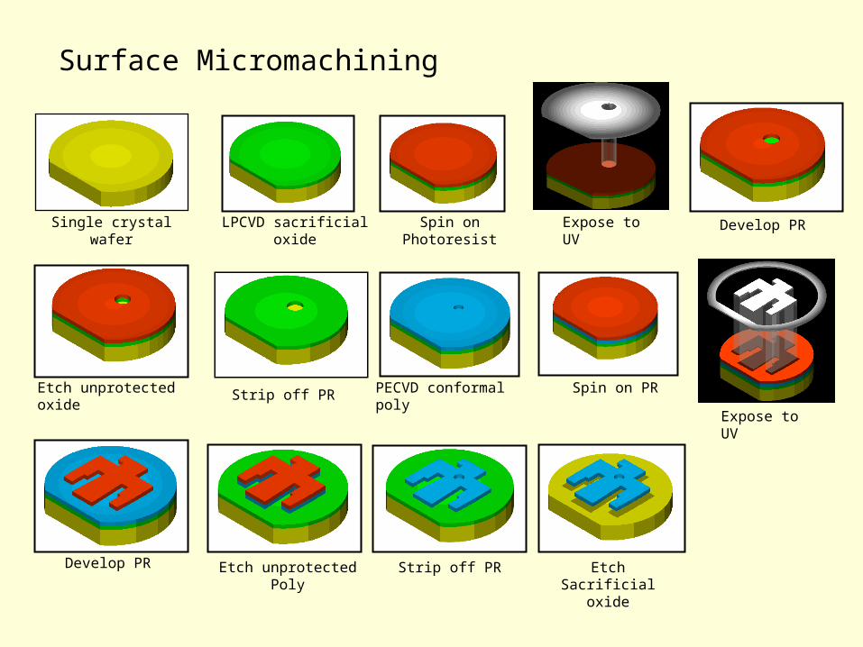
Single crystal wafer LPCVD sacrificial oxide Spin on Photoresist Expose to UV Develop PR
Etch unprotected oxide Strip off PR PECVD conformal poly Spin on PR
Expose to UV
Develop PR Etch unprotected Poly
Strip off PR Etch Sacrificial oxide
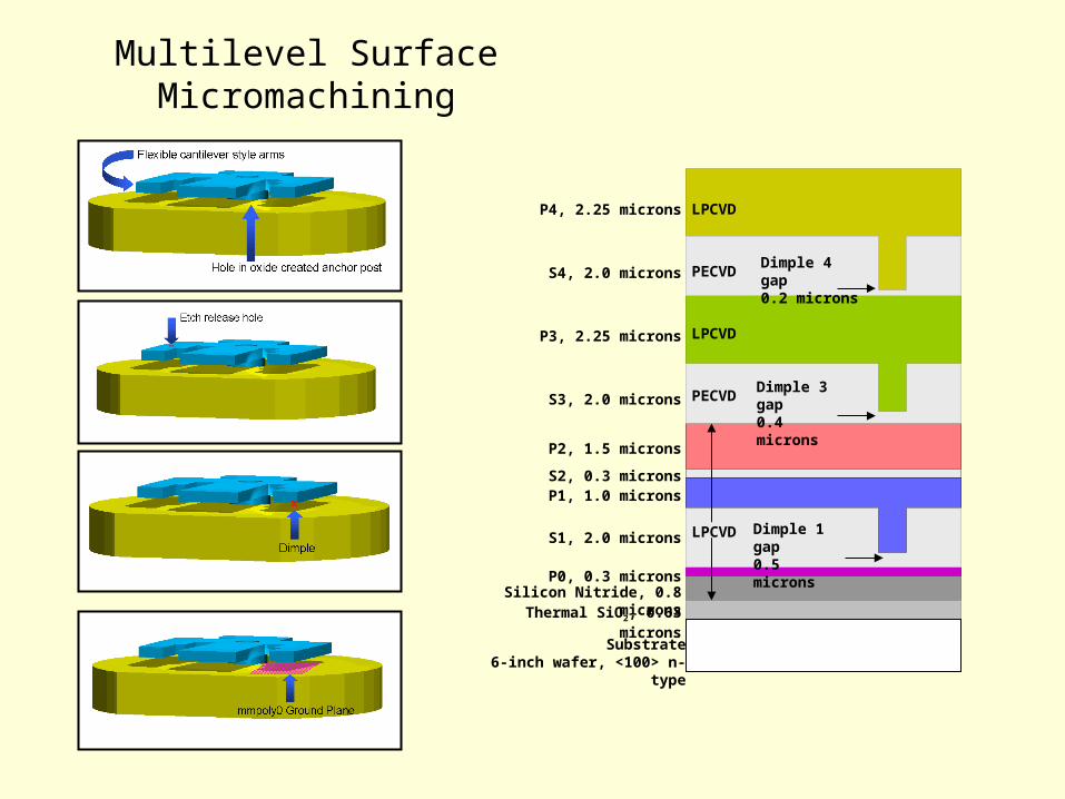
Multilevel Surface Micromachining
Thermal SiO2, 0.63 micronsSilicon Nitride, 0.8 microns
P0, 0.3 microns
S1, 2.0 microns
P1, 1.0 micronsS2, 0.3 microns
Substrate6-inch wafer, <100> n-type
P2, 1.5 microns
S3, 2.0 microns
P3, 2.25 microns
S4, 2.0 microns
P4, 2.25 microns
LPCVD
LPCVD
PECVD
PECVD
Dimple 1 gap0.5 microns
Dimple 3 gap0.4 microns
Dimple 4 gap0.2 microns
LPCVD
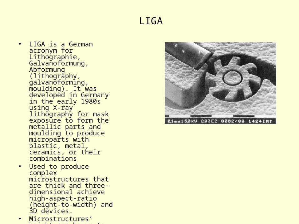
LIGA
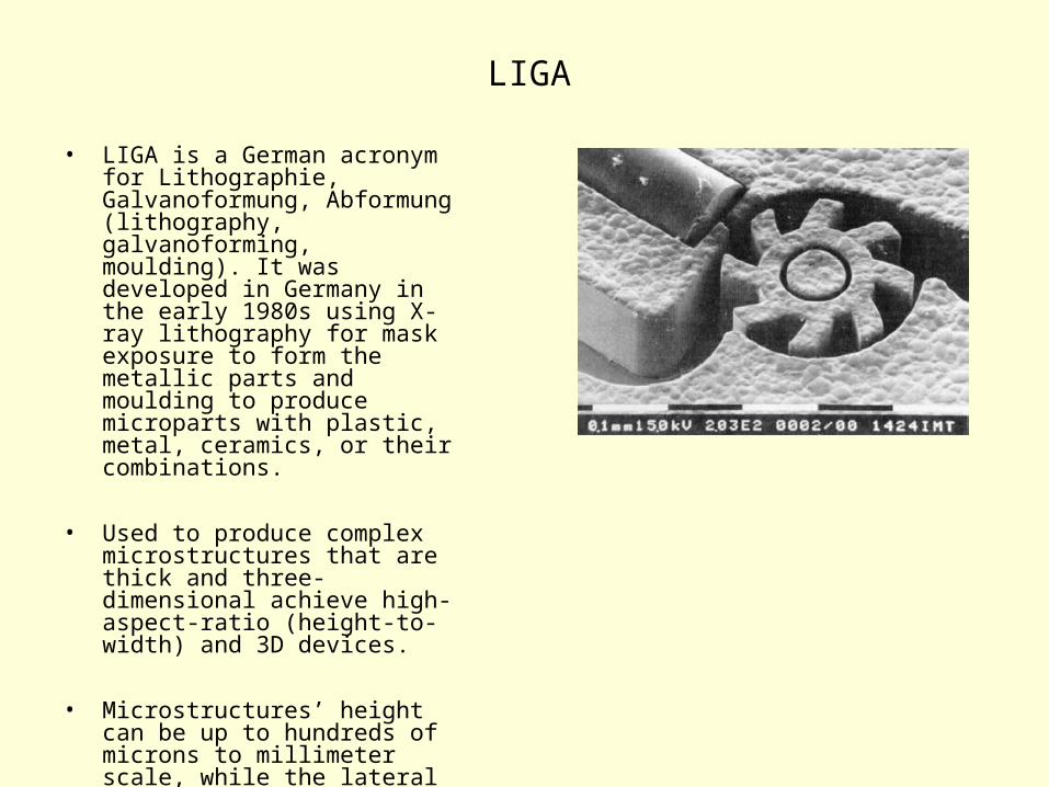
• LIGA is a German acronym for Lithographie, Galvanoformung, Abformung (lithography, galvanoforming, moulding). It was developed in Germany in the early 1980s using X-ray lithography for mask exposure to form the metallic parts and moulding to produce microparts with plastic, metal, ceramics, or their combinations
• Used to produce complex microstructures that are thick and three-dimensional achieve high-aspect-ratio (height-to-width) and 3D devices.
• Microstructures’ height can be up to hundreds of microns to millimeter scale, while the lateral resolution is kept at the submicron scale.
LIGA
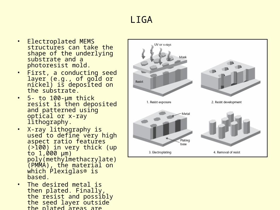
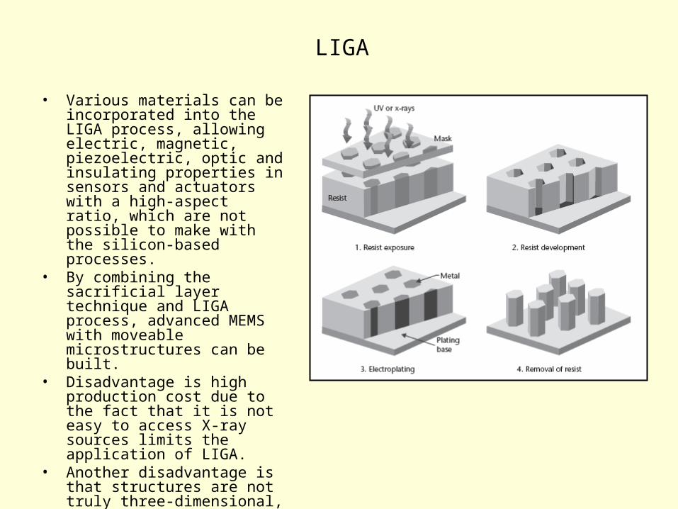
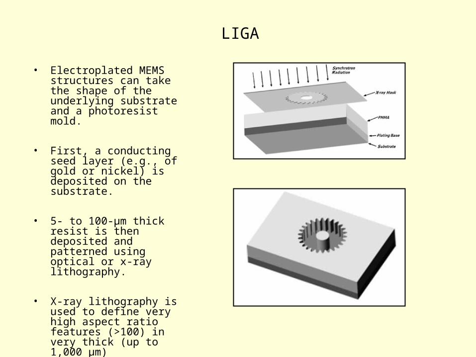
• Electroplated MEMS structures can take the shape of the underlying substrate and a photoresist mold.
• First, a conducting seed layer (e.g., of gold or nickel) is deposited on the substrate.
• 5- to 100-µm thick resist is then deposited and patterned using optical or x-ray lithography.
• X-ray lithography is used to define very high aspect ratio features (>100) in very thick (up to 1,000 µm) poly(methylmethacrylate) (PMMA), the material on which Plexiglas® is based.
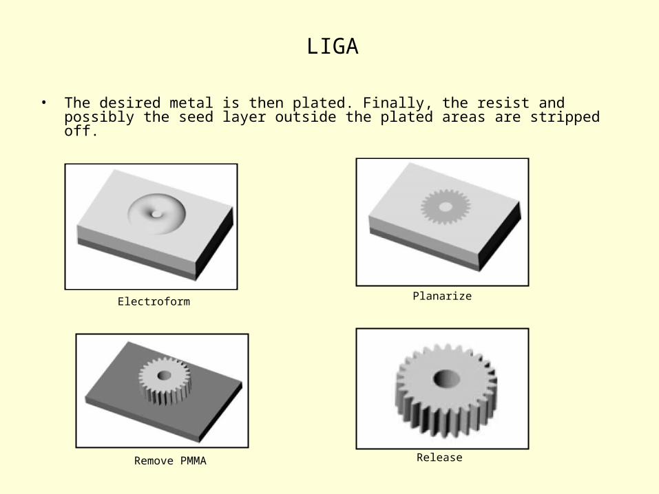
• The desired metal is then plated. Finally, the resist and possibly the seed layer outside the plated areas are stripped off.
LIGA
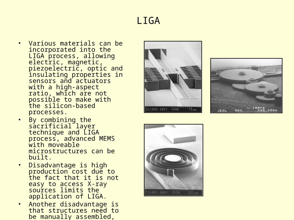
• Various materials can be incorporated into the LIGA process, allowing electric, magnetic, piezoelectric, optic and insulating properties in sensors and actuators with a high-aspect ratio, which are not possible to make with the silicon-based processes.
• By combining the sacrificial layer technique and LIGA process, advanced MEMS with moveable microstructures can be built.
• Disadvantage is high production cost due to the fact that it is not easy to access X-ray sources limits the application of LIGA.
• Another disadvantage is that structures are not truly three-dimensional, because the third dimension is always in a straight feature.
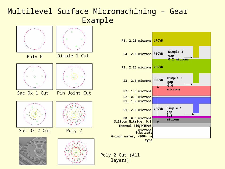
Multilevel Surface Micromachining – Gear Example
Poly 0
Sac Ox 1 Cut Pin Joint Cut
Sac Ox 2 Cut Poly 2
Poly 2 Cut (All layers)
Dimple 1 Cut
Thermal SiO2, 0.63 micronsSilicon Nitride, 0.8 microns
P0, 0.3 microns
S1, 2.0 microns
P1, 1.0 micronsS2, 0.3 microns
Substrate6-inch wafer, <100> n-type
P2, 1.5 microns
S3, 2.0 microns
P3, 2.25 microns
S4, 2.0 microns
P4, 2.25 microns
LPCVD
LPCVD
PECVD
PECVD
Dimple 1 gap0.5 microns
Dimple 3 gap0.4 microns
Dimple 4 gap0.2 microns
LPCVD
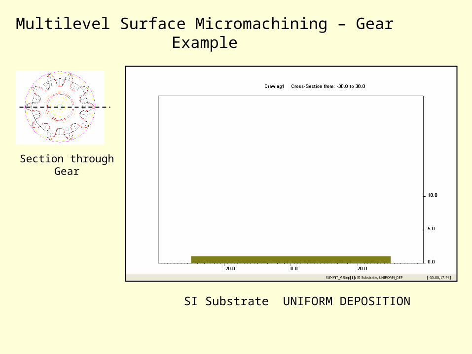
Multilevel Surface Micromachining – Gear Example
Section through Gear
SI Substrate UNIFORM DEPOSITION
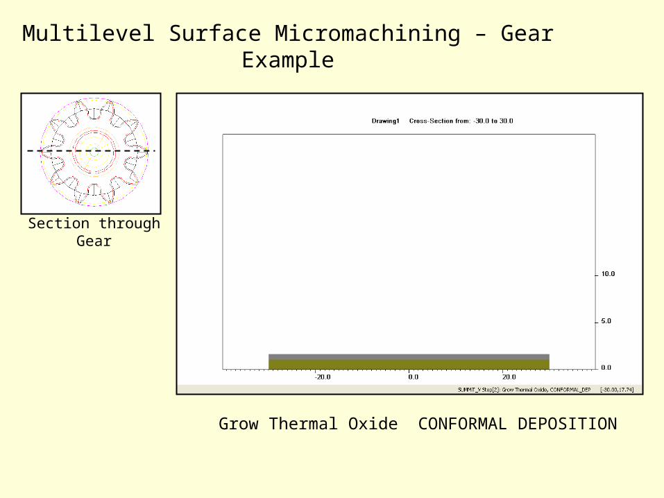
Multilevel Surface Micromachining – Gear Example
Section through Gear
Grow Thermal Oxide CONFORMAL DEPOSITION
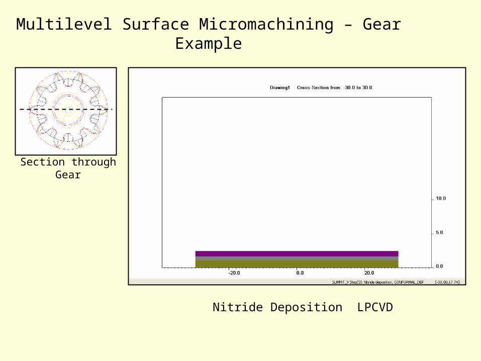
Multilevel Surface Micromachining – Gear Example
Section through Gear
Nitride Deposition LPCVD

Multilevel Surface Micromachining – Gear Example
Section through Gear
Nitride Etch DRY ETCH
Multilevel Surface Micromachining – Gear Example
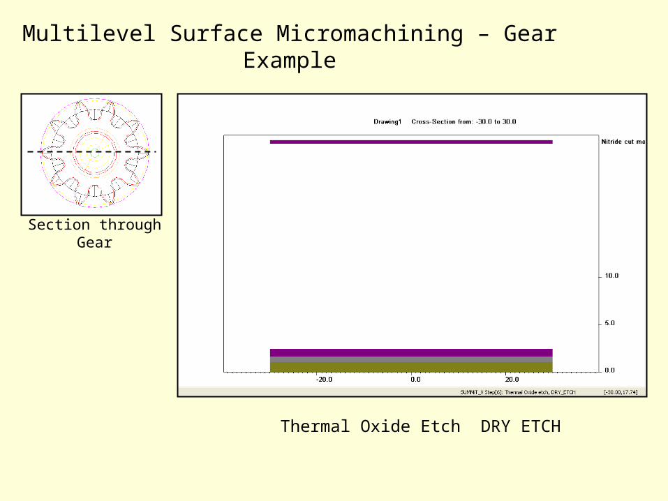
Section through Gear
Thermal Oxide Etch DRY ETCH
Multilevel Surface Micromachining – Gear Example
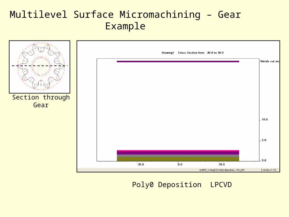
Section through Gear
Poly0 Deposition LPCVD
Multilevel Surface Micromachining – Gear Example
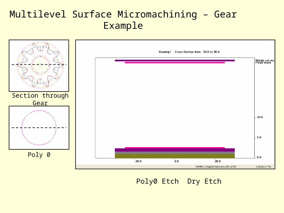
Section through Gear
Poly0 Etch Dry Etch
Poly 0
Multilevel Surface Micromachining – Gear Example
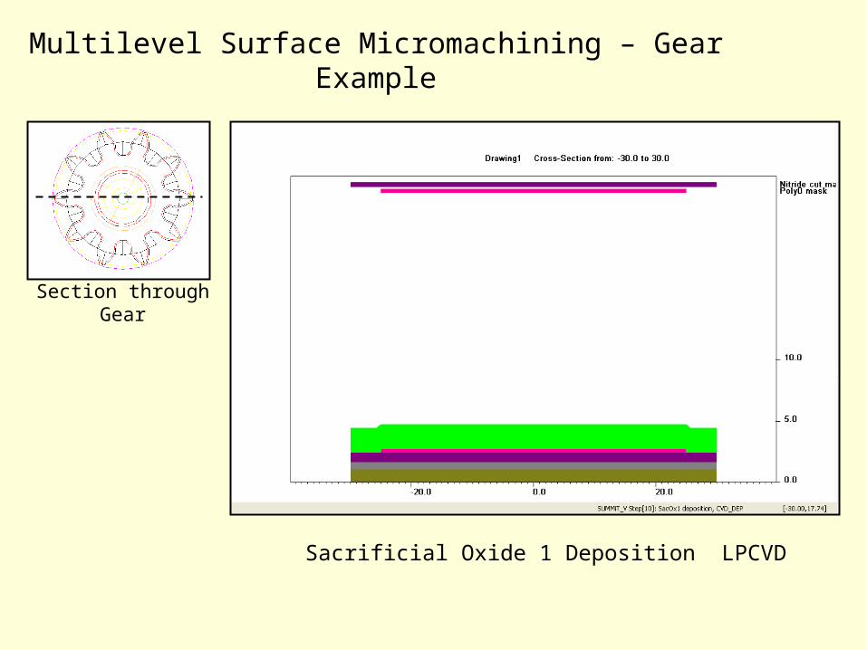
Section through Gear
Sacrificial Oxide 1 Deposition LPCVD
Multilevel Surface Micromachining – Gear Example
Section through Gear
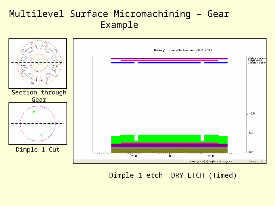
Dimple 1 etch DRY ETCH (Timed)
Dimple 1 Cut
Multilevel Surface Micromachining – Gear Example
Section through Gear
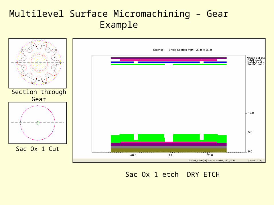
Sac Ox 1 etch DRY ETCH
Sac Ox 1 Cut
Multilevel Surface Micromachining – Gear Example
Section through Gear
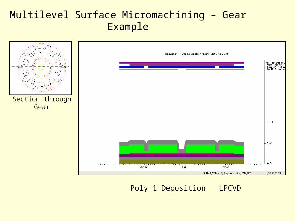
Poly 1 Deposition LPCVD
Multilevel Surface Micromachining – Gear Example
Section through Gear
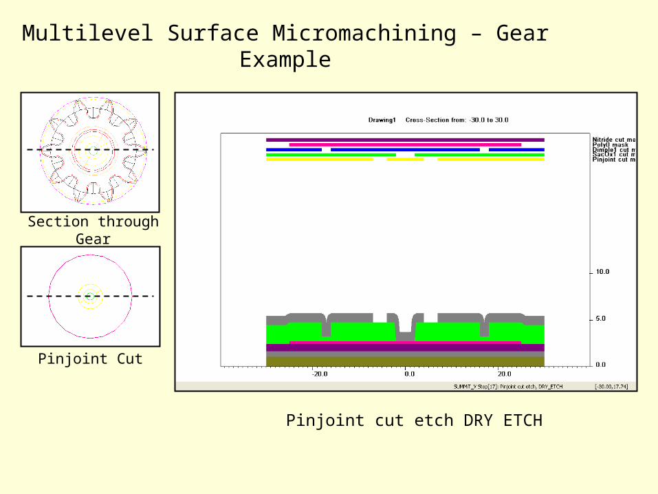
Pinjoint cut etch DRY ETCH
Pinjoint Cut
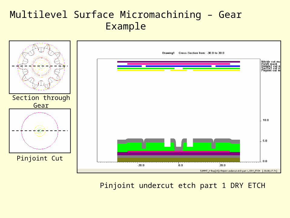
Multilevel Surface Micromachining – Gear Example
Section through Gear
Pinjoint undercut etch part 1 DRY ETCH
Pinjoint Cut
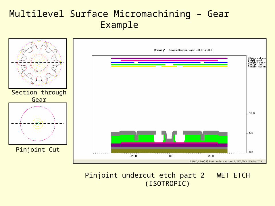
Multilevel Surface Micromachining – Gear Example
Section through Gear
Pinjoint undercut etch part 2 WET ETCH (ISOTROPIC)
Pinjoint Cut
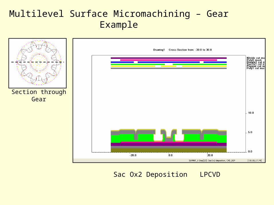
Multilevel Surface Micromachining – Gear Example
Section through Gear
Sac Ox2 Deposition LPCVD
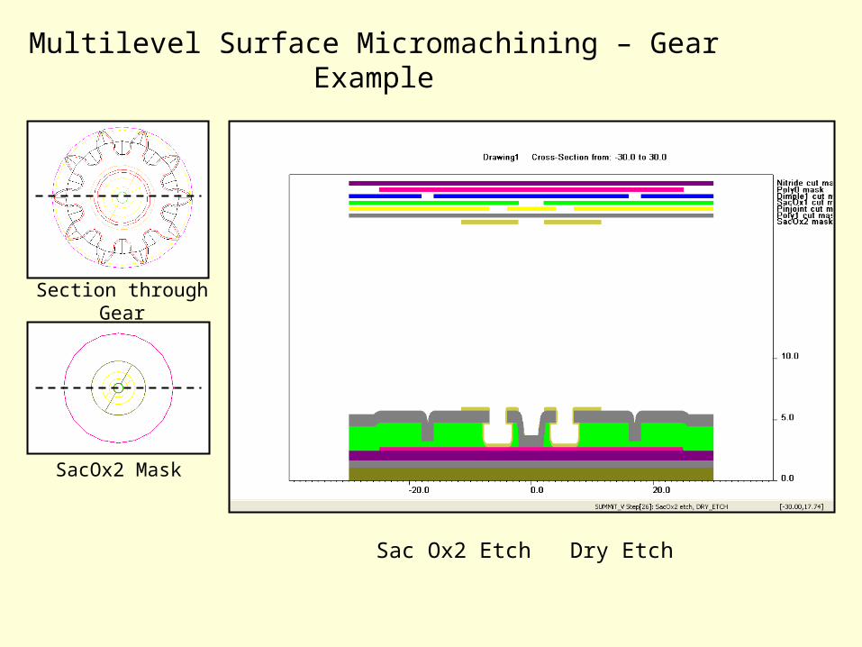
Multilevel Surface Micromachining – Gear Example
Section through Gear
Sac Ox2 Etch Dry Etch
SacOx2 Mask
Multilevel Surface Micromachining – Gear Example
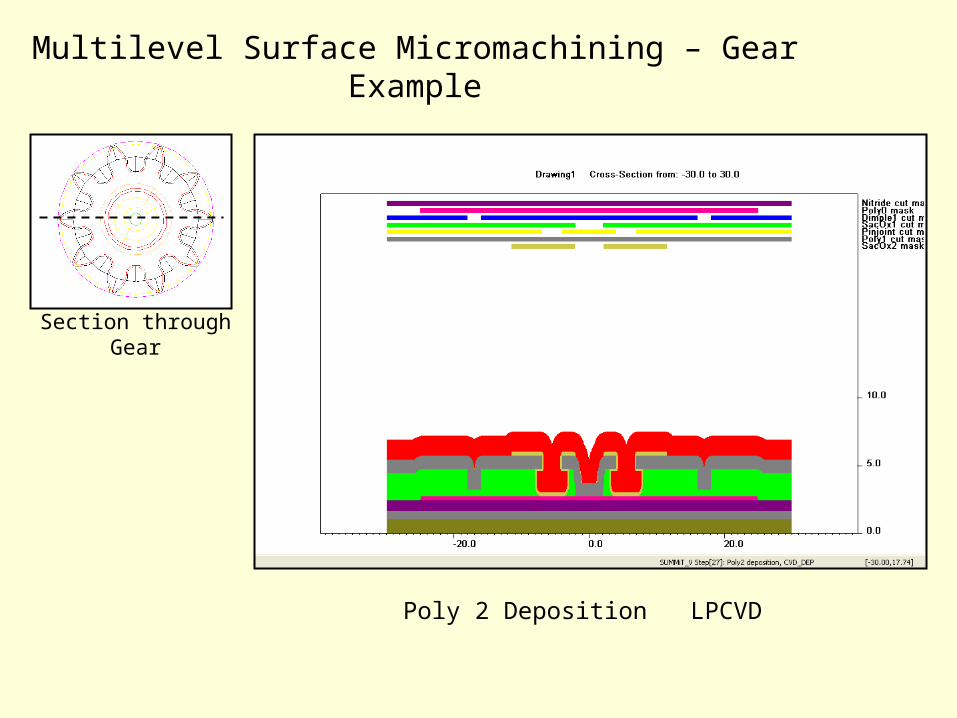
Section through Gear
Poly 2 Deposition LPCVD
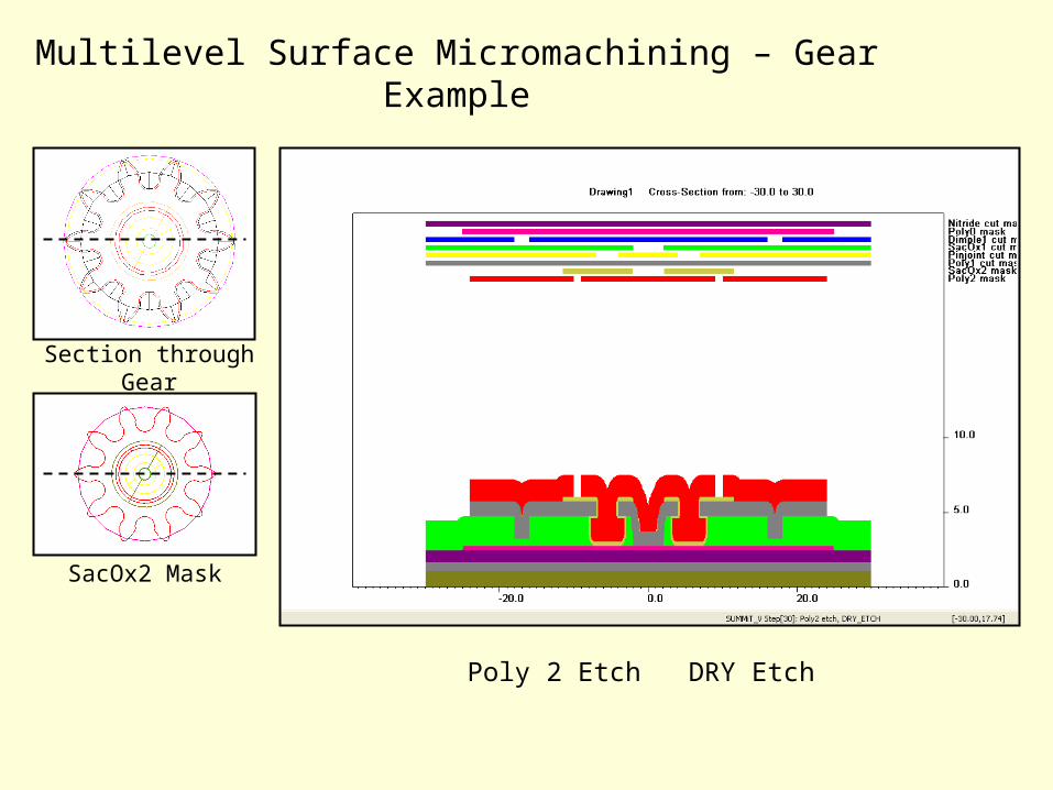
Multilevel Surface Micromachining – Gear Example
Section through Gear
Poly 2 Etch DRY Etch
SacOx2 Mask
Multilevel Surface Micromachining – Gear Example
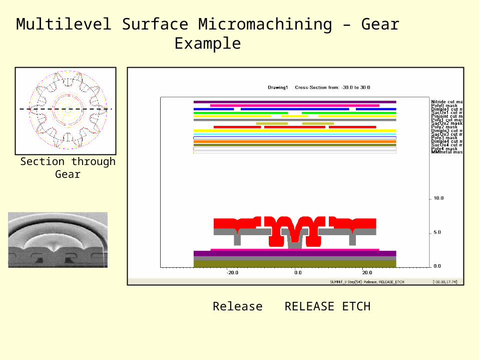
Section through Gear
Release RELEASE ETCH

Homework # 2
Consider Photochemical Fabrication Processes available in Jordan, and which can be used to demonstrate MEMS fabrication processes. Examples:
1. B&W Photography2. Zincograph3. PCB fabrication4. Glass Etching
Describe the following1. The process, photos etc.2. The physics and chemistry3. Equipment cost4. Possibility of implementing in a MEMS
lab
LIGA
• LIGA is a German acronym for Lithographie, Galvanoformung, Abformung (lithography, galvanoforming, moulding). It was developed in Germany in the early 1980s using X-ray lithography for mask exposure to form the metallic parts and moulding to produce microparts with plastic, metal, ceramics, or their combinations.
• Used to produce complex microstructures that are thick and three-dimensional achieve high-aspect-ratio (height-to-width) and 3D devices.
• Microstructures’ height can be up to hundreds of microns to millimeter scale, while the lateral resolution is kept at the submicron scale.
Electroplating
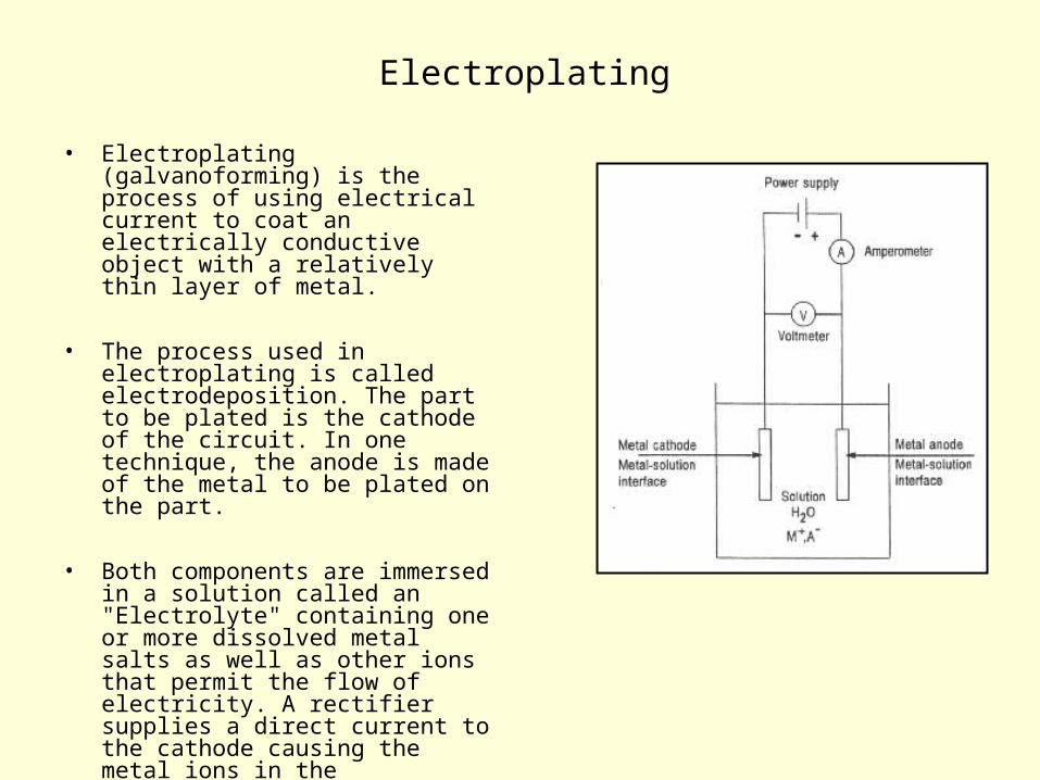
• Electroplating (galvanoforming) is the process of using electrical current to coat an electrically conductive object with a relatively thin layer of metal.
• The process used in electroplating is called electrodeposition. The part to be plated is the cathode of the circuit. In one technique, the anode is made of the metal to be plated on the part.
• Both components are immersed in a solution called an "Electrolyte" containing one or more dissolved metal salts as well as other ions that permit the flow of electricity. A rectifier supplies a direct current to the cathode causing the metal ions in the electrolyte solution to lose their charge and plate out on the cathode. As the electrical current flows through the circuit, the anode slowly dissolves and replenishes the ions in the bath.
LIGA
• Electroplated MEMS structures can take the shape of the underlying substrate and a photoresist mold.
• First, a conducting seed layer (e.g., of gold or nickel) is deposited on the substrate.
• 5- to 100-µm thick resist is then deposited and patterned using optical or x-ray lithography.
• X-ray lithography is used to define very high aspect ratio features (>100) in very thick (up to 1,000 µm) polymethylmethacrylate (PMMA), the material on which Plexiglas® is based
LIGA
• The desired metal is then plated. Finally, the resist and possibly the seed layer outside the plated areas are stripped off.
Electroform Planarize
Remove PMMA Release
LIGA
• Various materials can be incorporated into the LIGA process, allowing electric, magnetic, piezoelectric, optic and insulating properties in sensors and actuators with a high-aspect ratio, which are not possible to make with the silicon-based processes.
• By combining the sacrificial layer technique and LIGA process, advanced MEMS with moveable microstructures can be built.
• Disadvantage is high production cost due to the fact that it is not easy to access X-ray sources limits the application of LIGA.
• Another disadvantage is that structures need to be manually assembled, and they are not truly three-dimensional, because the third dimension is always in a straight feature.