Embed Size (px)
Citation preview
MEMS and Sensors Whitepaper Series
Silicon Nitride for MEMS Applications:
LPCVD and PECVD Process Comparison
January 2014
Whitepaper Topics: MEMS, sensors, microstructures, PECVD, LPCVD, HDPCVD, thin film, low stress, surface micromachining, fab process equipment.
About Us: Plasma-Therm is a U.S. based manufacturer of etch and thin film deposition equipment serving over 600 customers worldwide in silicon, compound semiconductor and related specialty markets. For nearly 40 years, we have enabled various process technologies by coupling reliable platforms with award-winning service. Plasma-Therm holds over 24 patents for innovation in plasma processing technologies, addressing applications in photo-mask, compound semiconductor, data storage and silicon-based devices. Included in our portfolio of solutions is deep silicon etching capability for MEMS, plasma dicing, and TSV. For more information, please visit www.plasmatherm.com.
Contact Information: Thierry Lazerand, Technical Marketing Director ([email protected]) David Lishan, Technical Marketing Director ([email protected]) Plasma-Therm Website (www.plasmatherm.com)
Silicon Nitride for MEMS Applications: LPCVD and PECVD Process Comparison
Copyright 2013 Plasma-Therm 2
Introduction
The MEMS industry grew by more than 10% in 2012, a year when the semiconductor industry experienced a 2% decline. The growth in MEMS was largely fueled by portable electronics with motion sensors and microphones in smartphones and tablets. Billions of MEMS devices have already been shipped and promising new applications in transportation, health care, sensor networks and structural monitoring have visionaries in the MEMS industry talking about trillions of MEMS devices. For the MEMS market to achieve the expected double digit annual growth, it is crucial that fabrication processes are both technically enabling and can support the demands of high volume device fabrication. One of the key factors in supporting this market growth is the extensive use of well-established CMOS and CMOS-compatible processes for large-scale MEMS manufacturing. Semiconductor processing infrastructure, equipment and technology has contributed to the successful scale up from 4” to 6”, 8”, and 12” diameter wafers while maintaining high production yields.
It is widely known that semiconductor processing is sensitive to limited thermal budgets. Excessive temperature can adversely affect metallized and diffused regions. As a result, high temperature processes must be completed upstream in the process flow or be substituted by low-temperature alternatives downstream. Historically, deposition of dielectric films has had a significant impact on the thermal budget. Lately, the industry trend is to reduce the deposition temperature for this process step. For example, thermal oxides using furnaces at 1000°C or higher have been supplanted by lower temperature solutions, such as Low Pressure Chemical Vapor Deposition (LPCVD), in the 600°C to 700°C range. Processes in the “less than 400°C” range are also commonly available with Plasma Enhanced Chemical Vapor Deposition (PECVD). Evolution in this area continues and have recently produced solutions such as high density plasma CVD (HDPCVD) and atomic layer deposition (ALD).
This paper will compare and contrast the use of LPCVD and PECVD by looking at key aspects of both technologies with a specific focus on MEMS applications. Differences in thermal budgets, film quality, manufacturability criteria (e.g. handling, maintenance, throughput), and performance (e.g. uniformity, repeatability) are discussed. The fundamental difference between the two technologies is that LPCVD relies upon thermally driven reactions using dichlorosilane (SiH2Cl2), while PECVD uses plasma with SiH4 to lower activation energies required for film formation. In a direct comparison, LPCVD is perceived as the high-volume, low-cost process and PECVD as the low-temperature alternative. There are, however, important nuances between the two and each technology have their associated advantages and limitations. Both technologies are frequently utilized for thin film deposition, but differ significantly in tool configurations, with LPCVD capable of processing over 100 wafers per run at 600°C to 800°C versus PECVD, which is typically a single wafer or relatively small batch operating between 200°C to 400°C.
Thin films provide dielectric functions (e.g. capacitors, interlayer insulation), encapsulation (e.g. moisture barriers), sacrificial layers, and anti-stiction surfaces in MEMS devices. One common example is the use of thin films to create membranes with desired characteristics for RF switches, microphones, opto-acoustic modulators and cantilevers. A more unique example is the use of electrostatically driven membranes to control micro-lenses for optical devices. This allows for active beam steering and compensation for optical misalignment caused by mechanical stress, temperature and atmospheric pressure. A third example is found in flammable gas detectors in the chemical industry. These detectors utilize micro machined planar pellistors where the heating and sensing elements are mounted on top of a silicon nitride diaphragm. Finally, MEMS microphones are based on thin membranes that

Silicon Nitride for MEMS Applications: LPCVD and PECVD Process Comparison
Copyright 2013 Plasma-Therm 3
can detect very subtle changes in pressure and have a higher bandwidth than conventional microphones.
The lower temperature processing regime of PECVD is more suitable for temperature sensitive MEMS devices using magnetic based materials. Emerging devices using these materials can potentially be used for applications that range from determining position and location (indoor and outdoor) to geophysical prospecting and medical diagnostics. Counterintuitively, an advantage of PECVD relates to film limited step coverage capability. The temperature of LPCVD promotes highly conformal films, and makes it less suitable for encapsulation where a cavity has previously been created with a sacrificial layer. In LPCVD, the deposition penetrates the cavity opening and film occurs on structures that interfere with their designed function. The lower temperature process regime of PECVD allows the cavity opening to seal with minimum deposition of material on the structures below.
Low Pressure Chemical Vapor Deposition (LPCVD) Process Overview
LPCVD is used in MEMS and semiconductor device processing for thin film deposition of dielectrics. LPCVD supports a variety of material compositions for compressive, neutral and tensile films, including polysilicon, oxides, nitrides and other dielectrics. For MEMS, LPCVD is commonly used to create films such as silicon nitride membranes with carefully defined properties. These films can range between a few nanometers to several micrometers in thickness with good conformity and uniformity. The “Low Pressure” in LPCVD refers to the sub-atmospheric processing pressure (often a few hundred mTorr). It is worth noting that LPCVD is very non-stoichiometric for low stress applications. SiNx (<250MPa) has a refractive index of 2.2, which goes up to 2.3 for very low stress (<100MPa).
The primary reaction mechanism for LPCVD is thermal decomposition on the wafer. These reactions require wafer surface temperatures typically in the 600°C to 800°C range. Furnace tube configurations are typically used to achieve those temperatures. Horizontal furnaces are the most common since they are easy to load manually, but vertical systems have become more popular throughout the 1990s due to improved automation, cleanliness and wafer film uniformity. LPCVD is a batch process and multiple wafers (up to 150 per batch) can be loaded at a time to increase the throughput and, thereby, lower the cost per wafer. A significant drawback of LPCVD is the high processing temperature range that can short junction contacts and undesirably drive doping into the substrate through diffusion. In some cases, it might be possible to pre-process wafers with LPCVD prior to CMOS or other temperature sensitive processing, but this might not always be feasible.
The formation of silicon nitride in LPCVD requires a silicon source, typically dichlorosilane (DCS) and ammonia (NH3). The gases are absorbed on the wafer surface, creating a thin silicon nitride film while the heterogeneous surface releases byproduct in the form of volatile gases. The furnace tube (quartz) is maintained at a standby temperature, usually about 400°C, when the quartz boat with the wafers is introduced into the reaction zone. At that time, the tube is evacuated and the temperature is ramped to the process set point. Process gases for deposition are then introduced with typical deposition rates ~20Å/min. Following deposition, the tube is purged, then evacuated and the temperature is then ramped back down to the standby condition. Ramp-up and ramp-down times are each in the 60-90 minutes range. Finally the process tube is vented and the boat with the wafers is withdrawn for cooling to below 100°C prior to unloading the wafers.
Silicon Nitride for MEMS Applications: LPCVD and PECVD Process Comparison
Copyright 2013 Plasma-Therm 4
This temperature cycling has an impact on particle generation both inside the process tube and the wafer boat. The combination of the accumulated thermal cycling creates film stresses that delaminates and particles are generated. This limits the number of consecutive runs between each cleaning cycle. Cleaning involves substituting parts and off-line wet cleaning. This type of maintenance will take the system offline for 4 to 6 hours. Once maintenance is completed, a requalification is required. Monitor wafers are evenly distributed throughout a boat carrier, loaded into the furnace and processed using a production recipe. The monitor wafers are inspected and process control parameters reviewed to ensure that they all are within specification before the furnace is ready for production.
Plasma Enhanced Chemical Vapor Deposition (PECVD) Process Overview
PECVD is a process, by which thin films of various materials can be deposited on substrates at lower temperature than that of standard LPCVD. The deposition temperature can be reduced significantly by utilizing plasma to lower the reaction activation energy. Plasma is generated by introducing reactant gases between two parallel electrodes; a grounded electrode and an RF energized electrode. The capacitive coupling between the two electrodes excites the reactant gases into a plasma state, which produces chemical species resulting in the deposition of thin films on the substrate. The substrate placed on the grounded electrode, is typically heated between 250°C and 350°C. The actual temperature depends on the specific film requirements.
The fundamental principles of plasma deposition are similar to plasma etching, except a film is deposited, rather than removed. PECVD process incorporates the following four fundamental steps:
1. Formation of plasma generated active gas species 2. Transport of the active species to the target substrate surface 3. Reaction at the target substrate surface 4. Pump down of the reaction by-products
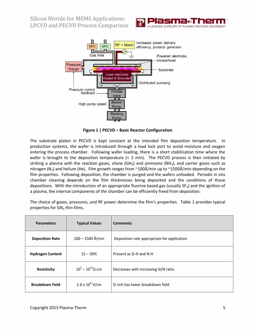
Figure 1 (on the following page) shows a generic PECVD reactor design. Gas delivery and vacuum handling follows standard practices. The pressure regime requires the use of a showerhead for uniform gas distribution. Heated internal components are used to increase film adherence and decrease the Meant Time Between Clean (MTBC) and particles.
Silicon Nitride for MEMS Applications: LPCVD and PECVD Process Comparison
Copyright 2013 Plasma-Therm 5
Figure 1 | PECVD – Basic Reactor Configuration
The substrate platen in PECVD is kept constant at the intended film deposition temperature. In production systems, the wafer is introduced through a load lock port to avoid moisture and oxygen entering the process chamber. Following wafer loading, there is a short stabilization time where the wafer is brought to the deposition temperature (< 2 min). The PECVD process is then initiated by striking a plasma with the reaction gases, silane (SiH4) and ammonia (NH3), and carrier gases such as nitrogen (N2) and helium (He). Film growth ranges from ~100Å/min up to ~1500Å/min depending on the film properties. Following deposition, the chamber is purged and the wafers unloaded. Periodic in situ chamber cleaning depends on the film thicknesses being deposited and the conditions of those depositions. With the introduction of an appropriate fluorine based gas (usually SF6) and the ignition of a plasma, the internal components of the chamber can be efficiently freed from deposition.
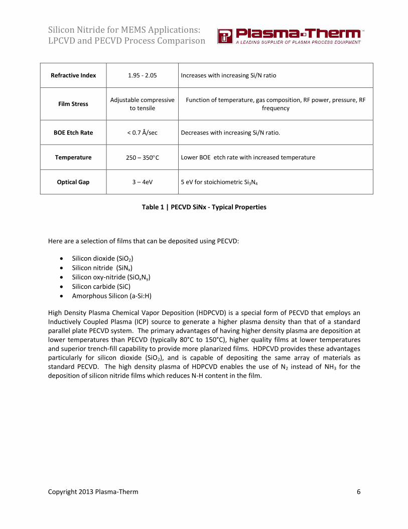
The choice of gases, pressures, and RF power determine the film’s properties. Table 1 provides typical properties for SiNx thin films.
Parameters Typical Values Comments
Deposition Rate 100 – 1500 Å/min Deposition rate appropriate for application
Hydrogen Content 15 – 30% Present as Si-H and N-H
Resistivity 105 – 1019Ω-cm Decreases with increasing Si/N ratio
Breakdown Field 1-6 x 10⁶ V/cm Si rich has lower breakdown field
Silicon Nitride for MEMS Applications: LPCVD and PECVD Process Comparison
Copyright 2013 Plasma-Therm 6
Refractive Index 1.95 - 2.05 Increases with increasing Si/N ratio
Film Stress Adjustable compressive
to tensile Function of temperature, gas composition, RF power, pressure, RF
frequency
BOE Etch Rate < 0.7 Å/sec Decreases with increasing Si/N ratio.
Temperature 250 – 350C Lower BOE etch rate with increased temperature
Optical Gap 3 – 4eV 5 eV for stoichiometric Si3N4
Table 1 | PECVD SiNx - Typical Properties
Here are a selection of films that can be deposited using PECVD:
Silicon dioxide (SiO2)
Silicon nitride (SiNx)
Silicon oxy-nitride (SiOxNy)
Silicon carbide (SiC)
Amorphous Silicon (a-Si:H)
High Density Plasma Chemical Vapor Deposition (HDPCVD) is a special form of PECVD that employs an Inductively Coupled Plasma (ICP) source to generate a higher plasma density than that of a standard parallel plate PECVD system. The primary advantages of having higher density plasma are deposition at lower temperatures than PECVD (typically 80°C to 150°C), higher quality films at lower temperatures and superior trench-fill capability to provide more planarized films. HDPCVD provides these advantages particularly for silicon dioxide (SiO2), and is capable of depositing the same array of materials as standard PECVD. The high density plasma of HDPCVD enables the use of N2 instead of NH3 for the deposition of silicon nitride films which reduces N-H content in the film.

Silicon Nitride for MEMS Applications: LPCVD and PECVD Process Comparison
Copyright 2013 Plasma-Therm 7
LPCVD vs. PECVD
LPCVD and PECVD are two different means to achieve a similar goal, deposition of low-stress silicon nitride films. Table 2 provides an extensive comparison between the two techniques:
Parameters LPCVD PECVD
Production Batch Size (up to 8”) (for low stress silicon nitride)
≤100 wafers Single wafer/small batch
Process Temperature (compatibility with other processes)
600°C to 800°C 250°C to 350°C
Deposition Rate ~20 Å/min 1000 Å/min
Throughput (0.1μm film) – 75 wafers load (including overhead)
~19 WPH ~13 WPH
Throughput (2μm film) – 75 wafers load (including overhead)
~3.5 WPH ~1.5 WPH
Thickness Uniformity Within Wafer ≤4% at 3mm ≤4% at 3mm
Thickness Uniformity Within Batch <3% Single wafer
Thickness Uniformity run-to-run <3% <3%
Low Stress capability -50MPa to +50MPa -50MPa to +50MPa
Stress Uniformity With Batch Complex temperature gradient
required Single wafer
Film Hermeticity Very good Very good
Film Density Very good Good
Silicon Nitride for MEMS Applications: LPCVD and PECVD Process Comparison
Copyright 2013 Plasma-Therm 8
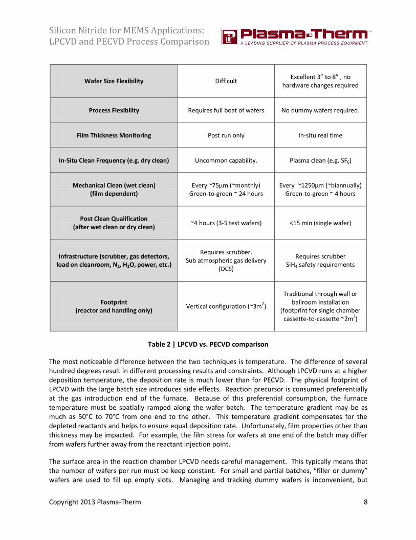
Wafer Size Flexibility Difficult Excellent 3” to 8” , no
hardware changes required
Process Flexibility Requires full boat of wafers No dummy wafers required.
Film Thickness Monitoring Post run only In-situ real time
In-Situ Clean Frequency (e.g. dry clean) Uncommon capability. Plasma clean (e.g. SF6)
Mechanical Clean (wet clean) (film dependent)
Every ~75μm (~monthly) Green-to-green ~ 24 hours
Every ~1250μm (~biannually) Green-to-green ~ 4 hours
Post Clean Qualification (after wet clean or dry clean)
~4 hours (3-5 test wafers) <15 min (single wafer)
Infrastructure (scrubber, gas detectors, load on cleanroom, N2, H2O, power, etc.)
Requires scrubber. Sub atmospheric gas delivery
(DCS)
Requires scrubber SiH4 safety requirements
Footprint (reactor and handling only)
Vertical configuration (~3m2)
Traditional through wall or ballroom installation
(footprint for single chamber cassette-to-cassette ~2m2)
Table 2 | LPCVD vs. PECVD comparison
The most noticeable difference between the two techniques is temperature. The difference of several hundred degrees result in different processing results and constraints. Although LPCVD runs at a higher deposition temperature, the deposition rate is much lower than for PECVD. The physical footprint of LPCVD with the large batch size introduces side effects. Reaction precursor is consumed preferentially at the gas introduction end of the furnace. Because of this preferential consumption, the furnace temperature must be spatially ramped along the wafer batch. The temperature gradient may be as much as 50°C to 70°C from one end to the other. This temperature gradient compensates for the depleted reactants and helps to ensure equal deposition rate. Unfortunately, film properties other than thickness may be impacted. For example, the film stress for wafers at one end of the batch may differ from wafers further away from the reactant injection point.
The surface area in the reaction chamber LPCVD needs careful management. This typically means that the number of wafers per run must be keep constant. For small and partial batches, “filler or dummy” wafers are used to fill up empty slots. Managing and tracking dummy wafers is inconvenient, but

Silicon Nitride for MEMS Applications: LPCVD and PECVD Process Comparison
Copyright 2013 Plasma-Therm 9
important in order to avoid catastrophic flaking due to excess film deposition or stress. To compensate for these inherent issues, it is possible to implement thermal in-situ cleans. However, this is not, very common. Alternatively, silicon carbide tube liners and boats can be used, but this is a significant cost addition.
Another issue for LPCVD is the inherent operating temperature that requires cycling from room temperature to as high as 800°C. For MEMS, this temperature cycling may generate stress on fragile device features that can cause irreversible structural damages. This is fundamentally different for PECVD, where a single wafer or small batch of wafers can be maintained with excellent temperature uniformity while sitting on actively temperature controlled chuck. The spatial consumption of reactants is avoided by utilizing a gas distribution showerhead. Non-uniformity in the case of PECVD results from gas flow dynamics at the wafer edge and is typically limited to the very outer few millimeters. The single wafer approach encourages within wafer and wafer-to-wafer film uniformity. The overall temperature excursion is much less for PECVD as the maximum cycling temperature is from room temperature to approximately 350°C.
The thin film performance characteristics are highly dependent on the uniformity and the film thickness. It is desirable to control these parameters during the film deposition. This is not possible with an LPCVD furnace with limited visual access to the wafers during processing. Instead, ongoing post run monitoring is required with process time adjustment (deposition rate drifts due to by-product buildup affecting pump conductance). Wafer-to-wafer process requirements for deposition rate control and changing furnace conditions demand frequent post run monitoring with test wafers and/or product wafers. In contrast, the PECVD chamber configuration allows in situ monitoring using optical measurements.
Plasma-Therm has developed a method for generating real-time monitoring of film thickness measurements during PECVD deposition as outlined in Figure 2. Plasma emission is used as the interrogating light source. Light reflected from the front and back surfaces of the growing film are guided through an optical lens and a waveguide to an external spectrometer for interferometric analysis. EndPointWorks®, a proprietary software application developed by Plasma-Therm, monitors the reflected light and calculates film deposition thickness and the real-time deposition rate. The calculated film thickness is compared with the desired thickness to provide a closed-loop monitoring and process control.
Figure 2 | In situ real time PECVD film thickness monitoring
Silicon Nitride for MEMS Applications: LPCVD and PECVD Process Comparison
Copyright 2013 Plasma-Therm 10
As previously discussed, PECVD utilizes silane and ammonia whereas LPCVD uses dichlorosilane and ammonia. Both sets of reactants are sensitive to air exposure and require proper handling. This includes appropriate chamber or furnace purging and the downstream effluent management. Depositing low stress silicon nitride in LPCVD requires a very high ratio of DCS:NH3. The higher ratio compared to conventional nitride, creates additional ammonium chloride by-product. This leads to several issues:
Lots of very small particles. During venting (loading or unloading) the potential for back streaming of ammonium chloride on to the wafers is particularly high.
Frequent cleaning of the reactor and quartz elements such as the boat and tube/liner is needed as there is no acceptable in situ clean technique.
The gases used in PECVD system form solid by-products that needs to be removed. In situ cleaning techniques greatly helps maintaining a clean reactor, but wet cleaning is infrequent. In addition, heated walls that are not temperature cycled between runs can reduce flaking. The MTBC depends specifically on the process and film thicknesses being run. LPCVD is limited in its flexibility to process thin and thick films consecutively due to the absence of the in situ clean capability. In contrast, plasma based PECVD systems have very effective built in cleaning capability.
Stress Control Techniques
Silicon nitride (SiNx) membranes are used in a wide range of MEMS applications, including optical beam steering and waveguides, thermal isolation for gas detection in the chemical industry and microphones. LPCVD deposits thin films that coat the entire wafer, front and back side. The difference in mechanical properties between the substrate and the deposited material, such as silicon nitride, will introduce mechanical stress. An equal amount of silicon nitride on the front and back side of a wafer equalizes the stress and the wafer remains flat. When silicon nitride is partially or fully removed from one of the sides, it will cause the wafer to bow and warp. The magnitude of the bow and warp will depend on the thickness of the silicon nitride, the amount of removed silicon and the thickness of the wafer substrate. Stress can be either tensile or compressive. Tensile stress bows the wafer in the direction of the nitride, whereas compressive stress bows the wafer away from the nitride. If the stress becomes too high (e.g. >800MPa), the nitride can crack and cause the film to delaminate. Lower stress nitrides (e.g. <200MPa) are available for stress sensitive applications, but insufficient tensile stress on silicon nitride membranes can cause sagging. Finding the right stress balance is important to ensure device reliability and performance. PECVD can be used to deposit both tensile and compressive films, which is highly useful for fine-tuning thin films properties and compensate for wafer bow.
Mechanical stress in silicon-based dielectrics can impact structural integrity similar to silicon nitride membranes, but also affect the electrical and optical performance of the device. If the thin film has too much compressive stress, it may blister and buckle. Conversely, too much tensile stress will cause the film to fracture. In both examples, the device integrity is compromised. In some applications thicker films are needed, such as, sacrificial layers in MEMS release processing (e.g. ~2μm). At these film thicknesses, even moderate film stresses will cause significant wafer bow. The wafer might remain intact, but subsequent processing steps, such as deep reactive ion etching (DRIE) or simple photolithography processing require flat wafers. The implication of less than optimal wafer bow translates into processing yield loss.
Silicon Nitride for MEMS Applications: LPCVD and PECVD Process Comparison
Copyright 2013 Plasma-Therm 11
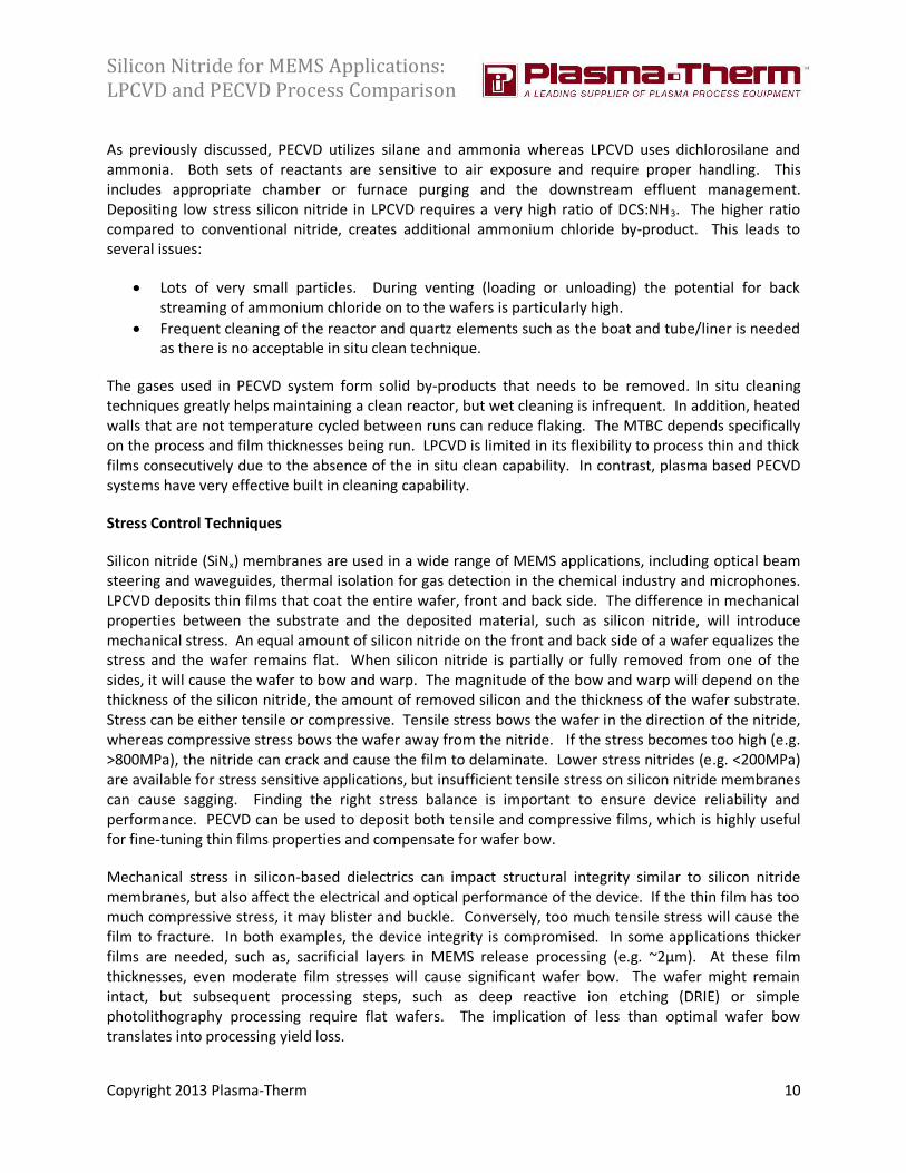
PECVD offers multiple means of stress control. An overview is provided in Table 3
PECVD Stress Control Parameter
Benefits Limitations
Temperature Provides ability to reduce stress at low
temperature Reduced film density with lower
temperature
Pressure/Power NH3 free process using N2 Only compressive at low pressures.
Lower deposition rate.
Alloy with O (e.g. SiON)
Provides a wide stress control window as well as other film properties
Not for applications requiring stoichiometric oxide or nitride films
Mixed Frequency Stress tunable from compressive to tensile Concerns for damage sensitive
applications
Helium Dilution Fine tune stress control for critical thin films
and tunable from compressive to tensile Slower deposition rates
Chemical Composition (e.g. enriched Si)
Provides good stress control for applications not index sensitive
Not recommended for index sensitive applications
Table 3 | PECVD SiNx Stress Control Methods
In LPCVD, the stress for silicon nitride is primarily controlled by the gas ratio of DCS:NH3. This approach has the drawback that the films are silicon rich non-stoichiometric. This leads to refractive index shifting from the standard values of ~2.0 to as high as ~2.3. The higher silicon content films are less resistant to KOH chemical etch with a resulting higher etch rate. Thus, using low stress silicon nitride LPCVD films may not be appropriate as an etch mask.
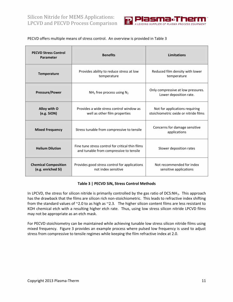
For PECVD stoichiometry can be maintained while achieving tunable low stress silicon nitride films using mixed frequency. Figure 3 provides an example process where pulsed low frequency is used to adjust stress from compressive to tensile regimes while keeping the film refractive index at 2.0.
Silicon Nitride for MEMS Applications: LPCVD and PECVD Process Comparison
Copyright 2013 Plasma-Therm 12
Figure 3 | PECVD SiNx stress control with mixed frequency
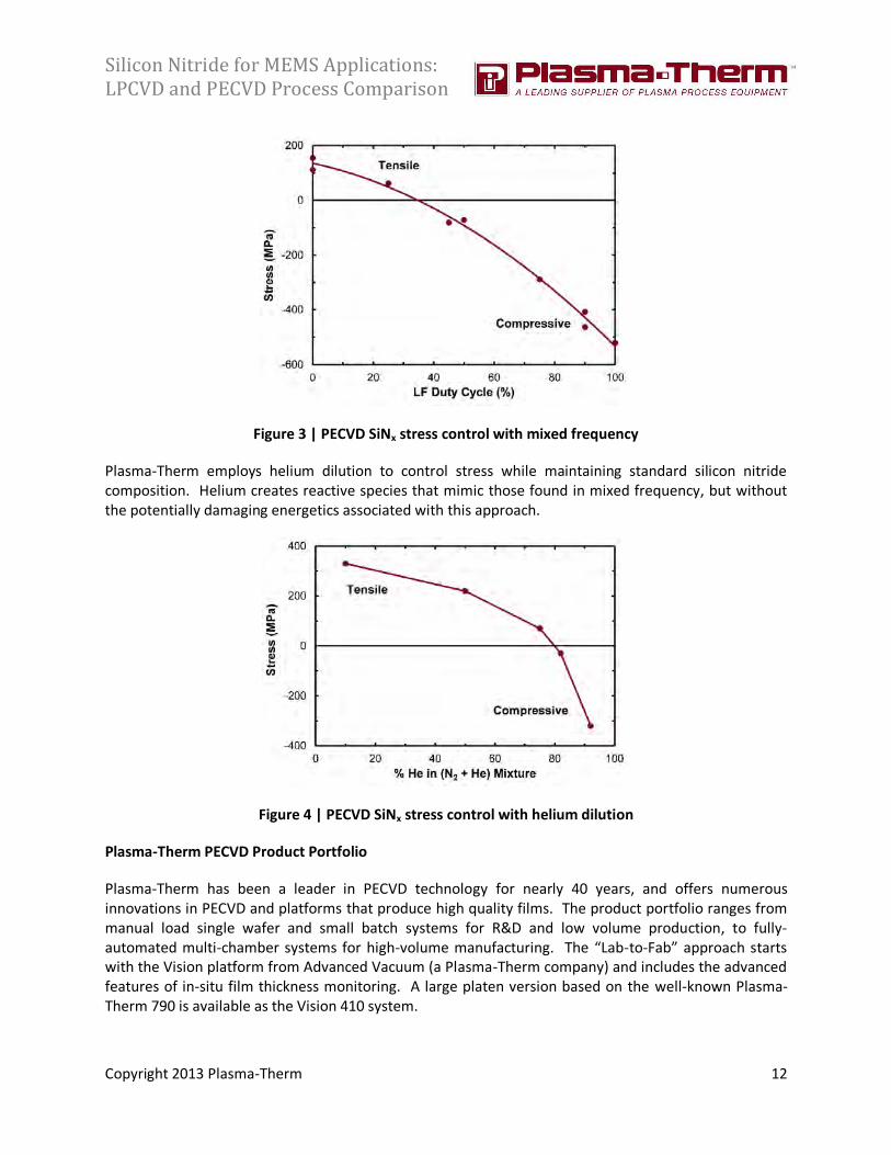
Plasma-Therm employs helium dilution to control stress while maintaining standard silicon nitride composition. Helium creates reactive species that mimic those found in mixed frequency, but without the potentially damaging energetics associated with this approach.
Figure 4 | PECVD SiNx stress control with helium dilution
Plasma-Therm PECVD Product Portfolio
Plasma-Therm has been a leader in PECVD technology for nearly 40 years, and offers numerous innovations in PECVD and platforms that produce high quality films. The product portfolio ranges from manual load single wafer and small batch systems for R&D and low volume production, to fully-automated multi-chamber systems for high-volume manufacturing. The “Lab-to-Fab” approach starts with the Vision platform from Advanced Vacuum (a Plasma-Therm company) and includes the advanced features of in-situ film thickness monitoring. A large platen version based on the well-known Plasma-Therm 790 is available as the Vision 410 system.

Silicon Nitride for MEMS Applications: LPCVD and PECVD Process Comparison
Copyright 2013 Plasma-Therm 13
The VERSALINE platform provides a load lock environment for more stringent process environment control and the flexibility to expand with multi-process chambers with cassette-to-cassette handling as capacity ramps. The VERSALINE® PECVD has the ability to deposit many different high-quality films while maximizing productivity and keeping the cost of ownership low. The parallel plate configuration is built to provide a clean processing environment and requires little maintenance. The product line of parallel plate reactors is augmented with high density plasma CVD configurations in both the VERSALINE platform, and the recently introduced APEX SLR platform from Advanced Vacuum.
The VERSALINE PECVD platform offers optimized surface heating, low damage stress control, easy chamber cleaning and in-situ film thickness monitoring. The in-house developed EndPointWorks® software package analyses plasma light reflected from the film interfaces during process and allows accurate film measurements. This results in superior process control and low wafer-to-wafer, lot-to-lot variability. Plasma-Therm’s VERSALINE® PECVD systems are modular and allow lower initial capital investment for single wafer processing capabilities. This can be expanded to batch loading for higher throughput to scale up with increasing manufacturing volumes. Finally, the PECVD systems can be used in conjunction with the DRIE process modules of the same VERSALINE platform, which are especially suited for high volume MEMS manufacturing.
For high throughput driven applications, the Large Area CVD platform (LAPECVD) can accommodate 3” to 8” planar cassette-to-cassette batch loading.
Vision 310 Vision 410 APEX SLR VERSALINE LAPECVD
(Note: VERSALINE and LAPECVD shown are multi-chamber installations)
Silicon Nitride for MEMS Applications: LPCVD and PECVD Process Comparison
Copyright 2013 Plasma-Therm 14
Summary and Conclusions
CVD is used in the semiconductor and MEMS industry to deposit high quality and highly uniform silicon nitride based films for device fabrication. This paper discusses two common methods for depositing low stress silicon nitride films, PECVD and LPCVD. Although they differ significantly in configurations (large batch vs. single wafer/small batch) and temperature regime, they both have merits and disadvantages. Throughput tends to be superior in LPCVD, however, particle control and wafer-to-wafer uniformity of film properties is better controlled in PECVD systems. The capability of in-situ plasma cleans and real time process monitoring as well as single sided deposition are distinct advantages of PECVD.
With over 20 years of deploying high quality and robust systems with excellent reliability track record and over 15 consecutive years of award winning service, Plasma-Therm offers industry leading PECVD systems with unique capabilities.
Acknowledgements: The authors appreciate useful discussions and contribution of Dr. Ken Mackenzie, Principal Scientist at Plasma-Therm LLC.
Contact Information:
Thierry Lazerand, Technical Marketing Director ([email protected]) David Lishan, Technical Marketing Director ([email protected])
Plasma-Therm (www.plasmatherm.com)