Embed Size (px)
Citation preview
MEMRISTOR-BASED COMPUTING ARCHITECTURE: DESIGN METHODOLOGIES AND CIRCUIT TECHNIQUES POLYTECHNIC INSTITUTE OF NEW YORK UNIVERSITY MARCH 2013 FINAL TECHNICAL REPORT
APPROVED FOR PUBLIC RELEASE; DISTRIBUTION UNLIMITED
STINFO COPY
AIR FORCE RESEARCH LABORATORY INFORMATION DIRECTORATE
AFRL-RI-RS-TR-2013-083
UNITED STATES AIR FORCE ROME, NY 13441 AIR FORCE MATERIEL COMMAND

NOTICE AND SIGNATURE PAGE Using Government drawings, specifications, or other data included in this document for any purpose other than Government procurement does not in any way obligate the U.S. Government. The fact that the Government formulated or supplied the drawings, specifications, or other data does not license the holder or any other person or corporation; or convey any rights or permission to manufacture, use, or sell any patented invention that may relate to them. This report was cleared for public release by the 88th ABW, Wright-Patterson AFB Public Affairs Office and is available to the general public, including foreign nationals. Copies may be obtained from the Defense Technical Information Center (DTIC) (http://www.dtic.mil). AFRL-RI-RS-TR-2013-083 HAS BEEN REVIEWED AND IS APPROVED FOR PUBLICATION IN ACCORDANCE WITH ASSIGNED DISTRIBUTION STATEMENT. FOR THE DIRECTOR: / S / / S / NATHAN MCDONALD JOSEPH A. CAROLI Work Unit Manager Acting Technical Advisor, Computing & Communications Division Information Directorate This report is published in the interest of scientific and technical information exchange, and its publication does not constitute the Government’s approval or disapproval of its ideas or findings.

REPORT DOCUMENTATION PAGE Form Approved
OMB No. 0704-0188 Public reporting burden for this collection of information is estimated to average 1 hour per response, including the time for reviewing instructions, searching data sources, gathering and maintaining the data needed, and completing and reviewing the collection of information. Send comments regarding this burden estimate or any other aspect of this collection of information, including suggestions for reducing this burden to Washington Headquarters Service, Directorate for Information Operations and Reports, 1215 Jefferson Davis Highway, Suite 1204, Arlington, VA 22202-4302, and to the Office of Management and Budget, Paperwork Reduction Project (0704-0188) Washington, DC 20503. PLEASE DO NOT RETURN YOUR FORM TO THE ABOVE ADDRESS. 1. REPORT DATE (DD-MM-YYYY)
MARCH 2013 2. REPORT TYPE
FINAL TECHNICAL REPORT 3. DATES COVERED (From - To)
OCT 2010 – OCT 2012 4. TITLE AND SUBTITLE MEMRISTOR-BASED COMPUTING ARCHITECTURE: DESIGN METHODOLOGIES AND CIRCUIT TECHNIQUES
5a. CONTRACT NUMBER FA8750-11-2-0046
5b. GRANT NUMBER N/A
5c. PROGRAM ELEMENT NUMBER 62788F
6. AUTHOR(S) Hai Li
5d. PROJECT NUMBER T2NC
5e. TASK NUMBER PO
5f. WORK UNIT NUMBER LY
7. PERFORMING ORGANIZATION NAME(S) AND ADDRESS(ES) Polytechnic Institute of New York University 2 MetroTech Center Brooklyn, NY 11201
8. PERFORMING ORGANIZATION REPORT NUMBER
N/A
9. SPONSORING/MONITORING AGENCY NAME(S) AND ADDRESS(ES) Air Force Research Laboratory/RITB 525 Brooks Road Rome NY 13441-4505
10. SPONSOR/MONITOR'S ACRONYM(S)
AFRL/RI 11. SPONSORING/MONITORING
AGENCY REPORT NUMBER AFRL-RI-RS-TR-2013-083
12. DISTRIBUTION AVAILABILITY STATEMENT Approved for Public Release; Distribution Unlimited. PA# 88ABW-2013-1319 Date Cleared: 20 Mar 2013
13. SUPPLEMENTARY NOTES 14. ABSTRACT Scientists have dreamed of information systems with cognitive human-like skills for years. However, constrained by the device characteristics and rapidly increasing design complexity under the traditional processing technology, little progress has been made in hardware implementation. The recently popularized memristor offers a potential break-through for neuromorphic computing because of its unique properties including nonvolatility extremely high fabrication density, and sensitivity to historic voltage/current behavior. In this project, we first investigated the memristor-based synapse design and the corresponding training scheme. Then, the design optimization and its implementation in multi-synapse systems were analyzed too. With the aid of a sharing training circuit and self-training mode, the performance and energy can be significantly improved. At last, a case study of an arithmetic logic unit (ALU) was designed to demonstrate the hardware implementation of a reconfigurable system built based on memristor synapses. All the circuit design, simulation, layout, and functionality verifications have been completed. 15. SUBJECT TERMS Memristor, synapse, neural network, adaptive system, neuromorphic systems
16. SECURITY CLASSIFICATION OF: 17. LIMITATION OF ABSTRACT
UU
18. NUMBER OF PAGES
19a. NAME OF RESPONSIBLE PERSON
NATHAN MCDONALD a. REPORT
U b. ABSTRACT
U c. THIS PAGE
U 19b. TELEPONE NUMBER (Include area code)
Standard Form 298 (Rev. 8-98) Prescribed by ANSI Std. Z39.18
37
ii
TABLE OF CONTENTS
Section Page
LIST OF FIGURES………………………………………………………………………………iv
LIST OF TABLES………………………………………………………………………………..vi
1.0 SUMMARY……………………………………………………………………………….1
2.0 INTRODUCTION………………………………………………………………………...1
3.0 METHODS, ASSUMPTIONS, AND PROCEDURES…………………………………...2
3.1 Memristor Theory…………………………………………………………………………2
3.2 The Memristor-based Logic Design………………………………………………………4
3.2.1 The Principle of Memristor-based Synapse……………………………………………….4
3.2.2 Synapse Training Circuit………………………………………………………………….4
3.2.3 Multi-synapse Training Scheme…………………………………………………………..6
3.2.4 Training Block Sharing Scheme…………………………………………………………..8
3.2.5 Two-level OR Neuron Training Strategy…………………………………………………8
3.2.6 Ten-synapse Circuit……………………………………………………………………….9
3.3 Case Study – Synapse-based ALU Design………………………………………………10
3.3.1 1-bit Adder-Subtractor Block……………………………………………………………10
3.3.2 Binary Counter…………………………………………………………………………...11
3.3.3 Decade Counter…………………………………………………………………………..12
3.3.4 4-bit ALU as Adder, Subtractor, and Decade Counter…………………………………..14
3.3.5 8-bit ALU as Adder, Subtractor, and Decade Counter…………………………………..14
4.0 RESULTS AND DISCUSSION…………………………………………………………18
iii
4.1 Simulation Verification of Memristor-based Logic Design…………………………...18
4.1.1 The Memristor-based Synapse…………………………………………………………...18
4.1.2 Synapse Training Circuit………………………………………………………………...19
4.1.3 Asymmetric Gate Design………………………………………………………………...20
4.1.4 2-Synapse Design with an OR Logic Neuron……………………………………………21
4.1.5 Self-training mode……………………………………………………………………….23
4.1.6 Power Analysis…………………………………………………………………………..23
4.2 The Functionality Verification of 8-bit ALU Design……………………………………24
4.2.1 Addition………………………………………………………………………………….24
4.2.2 Subtraction…………………………………………………………………………….....25
4.2.3 Binary Counting………………………………………………………………………….25
5.0 CONCLUSIONS………………………………………………………………………...26
6.0 REFERENCES…………………………………………………………………………..26
APPENDIX A - Publications and Presentations…………………………………………………28
LIST OF ABBREVIATIONS AND ACRONYMS……………………………………………..29

iv
LIST OF FIGURES
Figure Page
1 TiO2 thin-film memristor…………………………………………………………………3
2 A memristor-based synapse design………………………………………………………..4
3 Synapse training circuit symbol…………………………………………………………...5
4 Synapse training circuit diagram…………………………………………………….........5
5 Synapse together with training circuit…………………………………………………….6
6 Two-input neuron structure………………………………………………………………6
7 Training sharing distribution circuit………………………………………………………7
8 2-synapse shared training circuit and sharing distribution circuit………………………8
9 Two-level OR neuron circuit and possible logic values table……………………………8
10 Two-synapse shared training strategy……………………………………………………..9
11 10-synapse OR neuron circuit……………………………………………………………..9
12 Timing diagram of 10-synapse circuit training………………………………………......10
13 Schematic of 1-bit adder-subtractor block……………………………………………..10
14 Schematic of 4-bit binary counter built with adder-subtractor blocks…………………12
15 Schematic of the modified adder-subtractor block to realized Eq. (9c)…………………13
16 Schematic of the modified adder-subtractor block to realized Eq. (9d)…………….....14
17 Schematic of a 4-bit ALU as adder, subtractor, and decade counter…………………….15
18 Schematic of a 8-bit ALU as adder, subtractor, and binary counter……………………..16
19 Layout of a 8-bit ALU as adder, subtractor, and binary counter………………………...17
20 Output response of a synapse when memristor is at high resistance state………………18
v
21 Output voltage of a memristor-based synapse vs. memristance…………………………19
22 The timing diagram of training circuit…………………………………………………19
23 The simulation result of memristor training……………………………………………20
24 A design with two synapses and its four possible outputs………………………………21
25 The 2-synapse training circuit an simulation results……………………………………..22
26 The timing diagram of a 2-synapse training procedure.……………………………….22
27 Self-training simulation.………………………………………………………………....23
28 Simulation results of the 8-bit adder.…………………………………………………….24
29 Simulation results of the 8-bit subtractor..……………………………………………..25
30 Simulation results of the 8-bit binary counter..………………………………………...25

vi
LIST OF TABLES
Table Page
1 Training Circuit Operation Conditions……………………………………………………5
2 Training Sharing Circuit Operation………………………………………………………7
3 Synapse Input Pairs for Different Logic Values…………………………………………..7
4 Sizing of INV1 and Q1…………………………………………………………………..20
5 Synapse Power Consumption Analysis………………………………………………….24
Approved for Public Release; Distribution Unlimited.
1
1.0 SUMMARY
Scientists have dreamed of information systems with cognitive human-like skills for years. However, constrained by the device characteristics and rapidly increasing design complexity under the traditional processing technology, little progress has been made in hardware implementation. The recently popularized memristor offers a potential break-through for neuromorphic computing because of its unique properties including nonvola-tilely, extremely high fabrication density, and sensitivity to historic voltage/current be-havior. In this project, we first investigated the memristor-based synapse design and the corre-sponding training scheme. Then, the design optimization and its implementation in multi-synapse systems were analyzed too. With the aid of sharing training circuit and self-training mode, the performance and energy can be significantly improved. At last, a case study of an arithmetic logic unit (ALU) was designed to demonstrate the hardware im-plementation of reconfigurable system built based on memristor synapses. All the circuit design, simulation, layout, and functionality verifications have been completed.
2.0 INTRODUCTION
Neuromorphic computing architectures imitate natural neurobiological processes by mimicking the highly parallelized computing architecture of the biological brain. To real-ize such a novel architecture in hardware, at least two conditions need to be satisfied at the technology level: high integration density and ability to record the history of electric
signals. Neuromorphic computing architectures that have a large volume of memory and are adaptable to their environment have demonstrated great potential towards the devel-opment of high performance parallel computing systems [1]. Most of the research activi-ties have focused on software or the system level using conventional Von Neumann computer architectures [2-3]. Developing a neuromorphic architecture at the chip level by mimicking biological systems is another important direction. However, a biological scale hardware implementation based on traditional CMOS devices requires extremely high design complexity and cost, which is impractical. The existence of memristor was predicted as early as in 1971 [4], but the first physical realization that adopted that term was first reported thirty years later by Hewlett-Packard Laboratories (HP Labs) with their TiO2 thin-film device [5]. It soon became clear that many more materials with memristive properties had been reported since the 1960’s. Yet while these devices had some common behaviors, they each operated according to differ-ent physical phenomena. The unique properties of the memristor make it promising in neuromorphic computing systems. First, prototyped memristor devices have demonstrat-ed scalability at sub-10 nm scales. Accordingly, the memristor memories can achieve a high integration density of 100Gbits/cm
2, several orders higher than the popular flash memory technologies [4-5]. Second, the memristor device has an intrinsic and remarka-ble feature called “pinched hysteresis loop,” which means it can “remember” the total
Approved for Public Release; Distribution Unlimited.
2
electric charge flowing through it [4,6]. Third, memristance remains unchanged when power is turned off. Consequently, memristor-based memory combined with the high-integration capability and the pinched hysteresis characteristics can be applied to a mas-sively-parallel, large-scale neuromorphic computing processor architecture. Many memristor-based circuit designs have been explored, such as crossbar nonvolatile memory [8] and FPGA [9]. Strukov et al. integrated digital memory, programmable Boolean logic circuit, and neuron networks within a 3D hybrid CMOS/memristor struc-ture. Rajendran et al. proposed a memristor-based programmable threshold logic array [10] and used it in a synapse-neuron structure [11]. However, training circuits and train-ing schemes for a memristor-based reconfigurable architecture design have not been fully explored yet. Therefore, in this project, we investigated memristor-based reconfigurable design tech-niques. The structure is built upon single memristor-based synapse and the corresponding training circuit design. An 8-bit ALU design built on synapse structures was used as a case study to demonstrate its potential in developing a neuromorphic computing proces-sor architecture. The ALU design composed of ~100 synapses can be adaptively trained to realize addition, subtraction, and binary counting functionalities. The circuit design, simulation, layout, and functionality verifications have been completed in the project.
3.0 METHODS, ASSUMPTIONS, AND PROCEDURES
3.1. Memristor Theory
Nearly forty years ago, Professor Chua predicted the existence of the memristor – the fourth fundamental circuit element, to complete the set of passive devices that previously included only the resistor, capacitor, and inductor [4]. The memristor uniquely defines the relationship between the magnetic flux ( ) and the electric charge ( ) passing through the device,
. (1) Considering that magnetic flux and electric charge are the integrals of voltage ( ) and current ( ) over time, respectively, the definition of memristor can be generalized as
( ) ( )
, (2)
where is a state variable and ( ) represents the instantaneous memristance, which varies over time. For a “ideal” memristor, neither ( ) nor ( ) can be expressed only as a function of current .
Approved for Public Release; Distribution Unlimited.
3
Based on this mathematical description, these devices remained primarily intellectual cu-riosities until HP Lab first used these relationships to described the memristive switching effect created by moving the doping front along TiO2 thin-film device [4]. Soon, more memristive systems were identified according to their behavior, to include spintronics [5-6], polymeric thin film [12-13], MgO based magnetic tunnel junctions (MTJ) [14-15], and AlAs/GaAs/AlAs quantum-well diodes [16]. An intrinsic and remarkable feature of the memristor is called “pinched hysteresis loop,” that is, memristors can “remember” the total electric charge flowing through them by changing their resistances (memristance) [17]. The unique properties create great oppor-tunities in future system design. For instance, HP researchers proposed a memristor-based architecture, which could change the standard paradigm of computing by enabling calculations to be performed in the chips where data is stored, rather than in a specialized central processing unit [18]. Moreover, the applications of this memristive behavior in electronic neural network have been extensively studied [19-20]. Figure 1(a) illustrates the conceptual view of Pt/TiO2/Pt structure: two orthogonal metal wires (Pt) serve as the top and bottom electrodes with a thick titanium dioxide film sand-wiched in between. A perfect TiO2 structure in its natural state is as an insulator. Howev-er, the conductivity of oxygen-deficient titanium dioxide (TiO2-x) is much higher. By moving the doping front under proper electrical excitations, intermediate memristive states can be achieved. We use RH and RL to denote the total resistance when a TiO2 memristor is fully undoped (maximum high resistance) and doped (minimum low re-sistance), respectively. The overall memristance is then the equivalent of two serially-connected resistors, as shown in Figure 1(b). That is
M (α) = α · RL + (1 − α) · RH, (3) where α (0 ≤ α ≤ 1) is the relative doping front position, which is the ratio of the doping front position over the total thickness of the TiO2 device.
(a) TiO2 Memristor Stucture (b) Equivalent Circuit
Figure 1. TiO2 thin-film memristor
TiO2
Perfect TiO2
Metal (top electrode)
Metal (bottom electrode)
VDoping
front
TiO2-X
With oxygen vacancies
(1-α)·RH
α·RL
TE
BE
Approved for Public Release; Distribution Unlimited.
4
3.2. The Memristor-based Logic Design
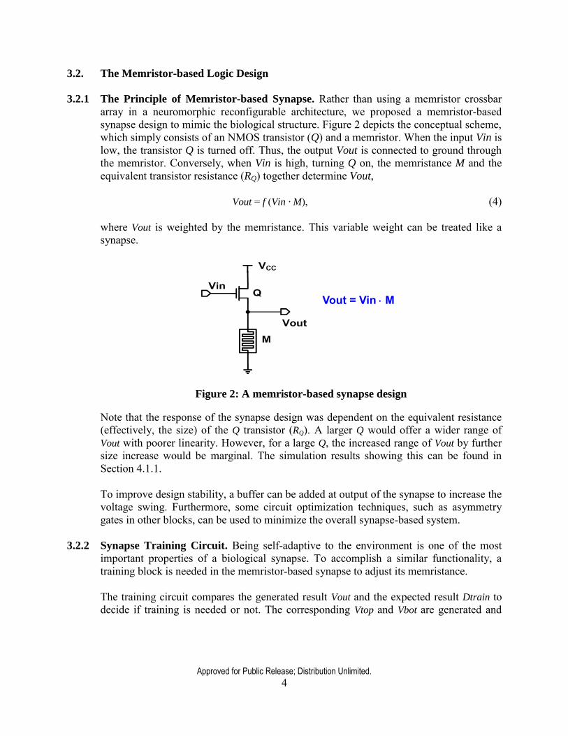
3.2.1 The Principle of Memristor-based Synapse. Rather than using a memristor crossbar
array in a neuromorphic reconfigurable architecture, we proposed a memristor-based synapse design to mimic the biological structure. Figure 2 depicts the conceptual scheme, which simply consists of an NMOS transistor (Q) and a memristor. When the input Vin is low, the transistor Q is turned off. Thus, the output Vout is connected to ground through the memristor. Conversely, when Vin is high, turning Q on, the memristance M and the equivalent transistor resistance (RQ) together determine Vout,
Vout = f (Vin · M), (4) where Vout is weighted by the memristance. This variable weight can be treated like a synapse.
Figure 2: A memristor-based synapse design
Note that the response of the synapse design was dependent on the equivalent resistance (effectively, the size) of the Q transistor (RQ). A larger Q would offer a wider range of Vout with poorer linearity. However, for a large Q, the increased range of Vout by further size increase would be marginal. The simulation results showing this can be found in Section 4.1.1. To improve design stability, a buffer can be added at output of the synapse to increase the voltage swing. Furthermore, some circuit optimization techniques, such as asymmetry gates in other blocks, can be used to minimize the overall synapse-based system.
3.2.2 Synapse Training Circuit. Being self-adaptive to the environment is one of the most important properties of a biological synapse. To accomplish a similar functionality, a training block is needed in the memristor-based synapse to adjust its memristance.
The training circuit compares the generated result Vout and the expected result Dtrain to decide if training is needed or not. The corresponding Vtop and Vbot are generated and
Vout = Vin M
Approved for Public Release; Distribution Unlimited.
5
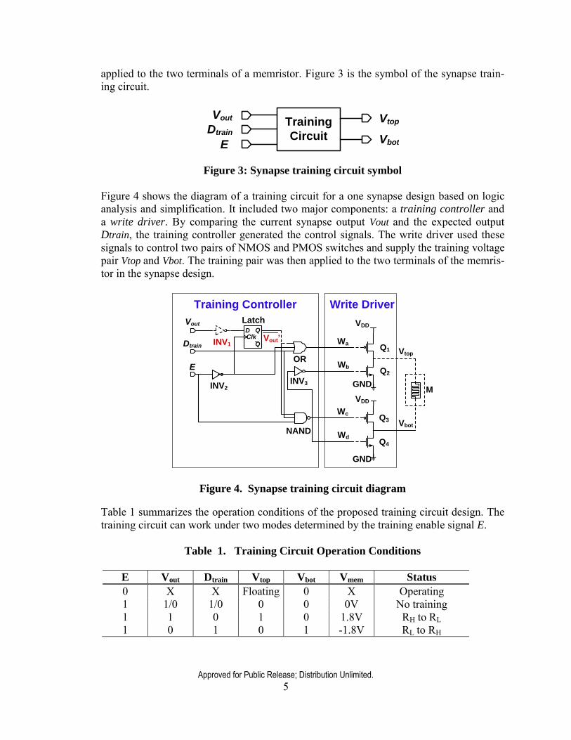
applied to the two terminals of a memristor. Figure 3 is the symbol of the synapse train-ing circuit.
Figure 3: Synapse training circuit symbol Figure 4 shows the diagram of a training circuit for a one synapse design based on logic analysis and simplification. It included two major components: a training controller and a write driver. By comparing the current synapse output Vout and the expected output Dtrain, the training controller generated the control signals. The write driver used these signals to control two pairs of NMOS and PMOS switches and supply the training voltage pair Vtop and Vbot. The training pair was then applied to the two terminals of the memris-tor in the synapse design.
Figure 4. Synapse training circuit diagram
Table 1 summarizes the operation conditions of the proposed training circuit design. The training circuit can work under two modes determined by the training enable signal E.
Table 1. Training Circuit Operation Conditions
E Vout Dtrain Vtop Vbot Vmem Status
0 X X Floating 0 X Operating 1 1/0 1/0 0 0 0V No training 1 1 0 1 0 1.8V RH to RL 1 0 1 0 1 -1.8V RL to RH
Training
Circuit E
Vout
Dtrain
Vtop
Vbot
M
E
Vout
Wa
Wb
Wc
Wd
VDD
VDD
GND
GND
NAND
OR
INV3
Write DriverTraining Controller
Vtop
Vbot
Q1
Q2
Q3
Q4
D QClk
QDtrainINV1
INV2
Vout’
Latch
Approved for Public Release; Distribution Unlimited.
6
* ‘0’ logic low; ‘1’ logic high, and ‘X’ unknown or don’t care. Operating mode: When E = 0, the synapse operated in the regular (read) mode; and
the training circuit was disabled. Training mode: The training circuit was enabled when E = 1. By comparing the cur-
rent synapse output Vout and the expected Dtrain, the training circuit generated Vtop and the Vbot applied to the two terminals of the memristor to update or keep its memristance. We define Vmem = Vtop – Vbot.
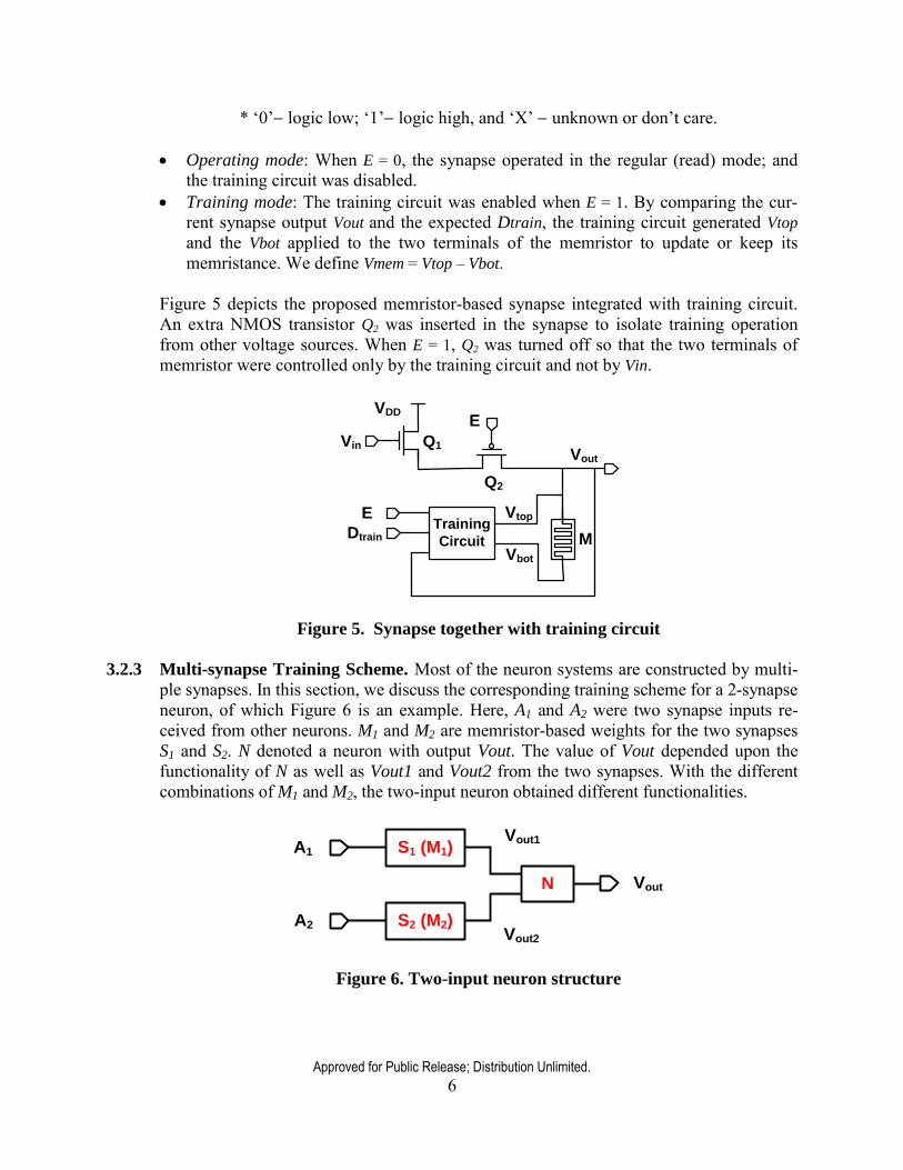
Figure 5 depicts the proposed memristor-based synapse integrated with training circuit. An extra NMOS transistor Q2 was inserted in the synapse to isolate training operation from other voltage sources. When E = 1, Q2 was turned off so that the two terminals of memristor were controlled only by the training circuit and not by Vin.
Figure 5. Synapse together with training circuit
3.2.3 Multi-synapse Training Scheme. Most of the neuron systems are constructed by multi-
ple synapses. In this section, we discuss the corresponding training scheme for a 2-synapse neuron, of which Figure 6 is an example. Here, A1 and A2 were two synapse inputs re-ceived from other neurons. M1 and M2 are memristor-based weights for the two synapses S1 and S2. N denoted a neuron with output Vout. The value of Vout depended upon the functionality of N as well as Vout1 and Vout2 from the two synapses. With the different combinations of M1 and M2, the two-input neuron obtained different functionalities.
Figure 6. Two-input neuron structure
Training
Circuit
E
Dtrain
Vtop
Vbot
VDD
Vin Q1
Q2
M
E
Vout
S1 (M1)A1
S2 (M2)A2
Vout
Vout2
Vout1
N
Approved for Public Release; Distribution Unlimited.
7
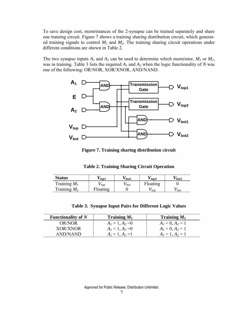
To save design cost, memristances of the 2-synapse can be trained separately and share one training circuit. Figure 7 shows a training sharing distribution circuit, which generat-ed training signals to control M1 and M2. The training sharing circuit operations under different conditions are shown in Table 2. The two synapse inputs A1 and A2 can be used to determine which memristor, M1 or M2, was in training. Table 3 lists the required A1 and A2 when the logic functionality of N was one of the following: OR/NOR, XOR/XNOR, AND/NAND.
Figure 7. Training sharing distribution circuit
Table 2. Training Sharing Circuit Operation
Status Vtop1 Vbot1 Vtop2 Vbot2
Training M1 Vtop Vbot Floating 0 Training M2 Floating 0 Vtop Vbot
Table 3. Synapse Input Pairs for Different Logic Values
Functionality of N Training M1 Training M2
OR/NOR A1 = 1, A2 =0 A1 = 0, A2 = 1 XOR/XNOR A1 = 1, A2 =0 A1 = 0, A2 = 1 AND/NAND A1 = 1, A2 =1 A1 = 1, A2 = 1
E
A1
A2
Vtop
Vbot
Transmission
Gate
Transmission
Gate
Vtop1
Vbot1
Vtop2
Vbot2
AND
AND
AND
AND
Approved for Public Release; Distribution Unlimited.
8
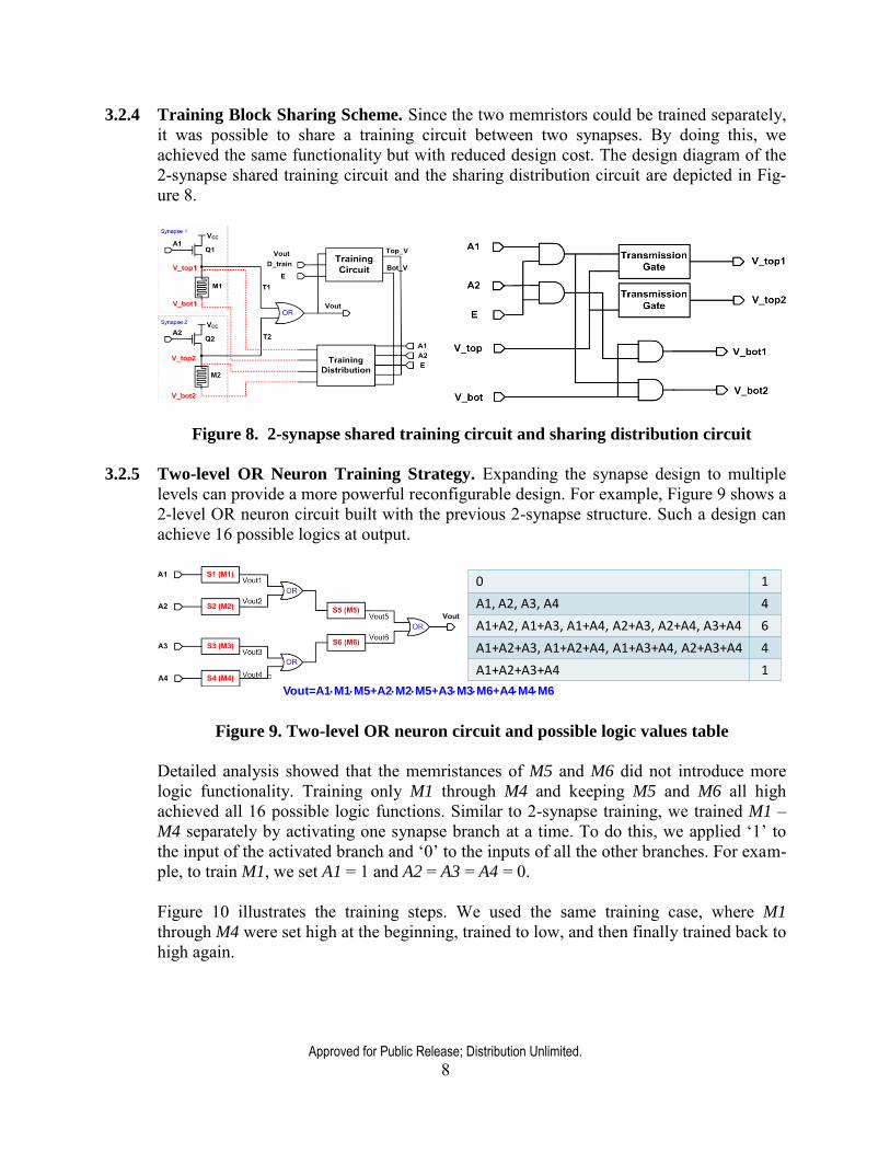
3.2.4 Training Block Sharing Scheme. Since the two memristors could be trained separately, it was possible to share a training circuit between two synapses. By doing this, we achieved the same functionality but with reduced design cost. The design diagram of the 2-synapse shared training circuit and the sharing distribution circuit are depicted in Fig-ure 8.
Figure 8. 2-synapse shared training circuit and sharing distribution circuit
3.2.5 Two-level OR Neuron Training Strategy. Expanding the synapse design to multiple levels can provide a more powerful reconfigurable design. For example, Figure 9 shows a 2-level OR neuron circuit built with the previous 2-synapse structure. Such a design can achieve 16 possible logics at output.
Figure 9. Two-level OR neuron circuit and possible logic values table
Detailed analysis showed that the memristances of M5 and M6 did not introduce more logic functionality. Training only M1 through M4 and keeping M5 and M6 all high achieved all 16 possible logic functions. Similar to 2-synapse training, we trained M1 – M4 separately by activating one synapse branch at a time. To do this, we applied ‘1’ to the input of the activated branch and ‘0’ to the inputs of all the other branches. For exam-ple, to train M1, we set A1 = 1 and A2 = A3 = A4 = 0. Figure 10 illustrates the training steps. We used the same training case, where M1 through M4 were set high at the beginning, trained to low, and then finally trained back to high again.
Vout=A1M1M5+A2M2M5+A3M3M6+A4M4M6
0 1
A1, A2, A3, A4 4
A1+A2, A1+A3, A1+A4, A2+A3, A2+A4, A3+A4 6
A1+A2+A3, A1+A2+A4, A1+A3+A4, A2+A3+A4 4
A1+A2+A3+A4 1
Approved for Public Release; Distribution Unlimited.
9
Figure 10. Two-synapse shared training strategy
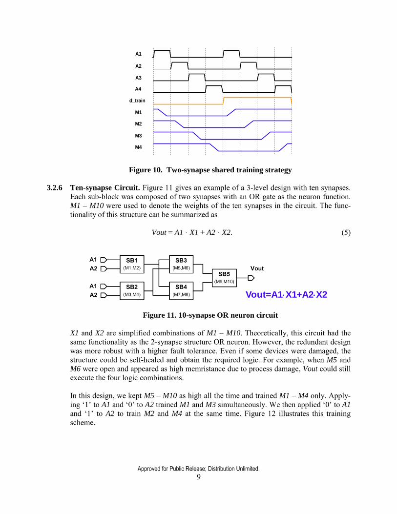
3.2.6 Ten-synapse Circuit. Figure 11 gives an example of a 3-level design with ten synapses.
Each sub-block was composed of two synapses with an OR gate as the neuron function. M1 – M10 were used to denote the weights of the ten synapses in the circuit. The func-tionality of this structure can be summarized as
Vout = A1 · X1 + A2 · X2. (5)
Figure 11. 10-synapse OR neuron circuit
X1 and X2 are simplified combinations of M1 – M10. Theoretically, this circuit had the same functionality as the 2-synapse structure OR neuron. However, the redundant design was more robust with a higher fault tolerance. Even if some devices were damaged, the structure could be self-healed and obtain the required logic. For example, when M5 and M6 were open and appeared as high memristance due to process damage, Vout could still execute the four logic combinations. In this design, we kept M5 – M10 as high all the time and trained M1 – M4 only. Apply-ing ‘1’ to A1 and ‘0’ to A2 trained M1 and M3 simultaneously. We then applied ‘0’ to A1 and ‘1’ to A2 to train M2 and M4 at the same time. Figure 12 illustrates this training scheme.
A1
A2
A3
A4
M1
M2
M3
M4
d_train
Vout=A1X1+A2X2
Approved for Public Release; Distribution Unlimited.
10
Figure 12. Timing diagram of 10-synapse circuit training
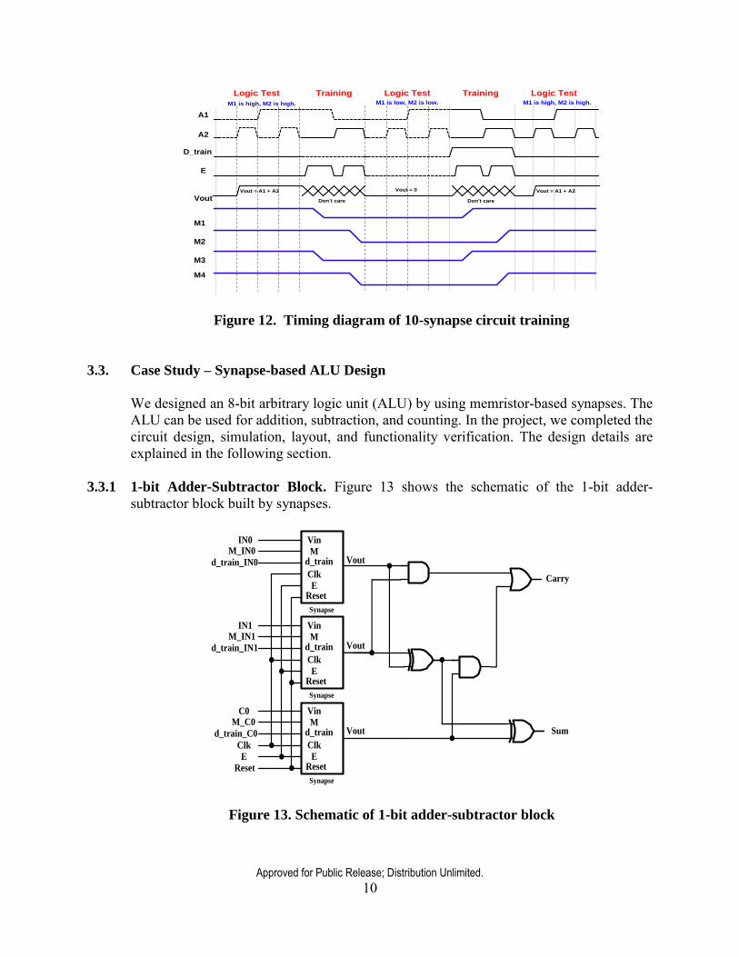
3.3. Case Study – Synapse-based ALU Design
We designed an 8-bit arbitrary logic unit (ALU) by using memristor-based synapses. The ALU can be used for addition, subtraction, and counting. In the project, we completed the circuit design, simulation, layout, and functionality verification. The design details are explained in the following section.
3.3.1 1-bit Adder-Subtractor Block. Figure 13 shows the schematic of the 1-bit adder-subtractor block built by synapses.
Vin
Md_train
Clk
EReset
Vout
Vin
Md_train
Clk
EReset
Vout
Vin
Md_train
Clk
EReset
Vout
Reset
E
Clk
C0M_C0
d_train_C0
IN1M_IN1
d_train_IN1
IN0M_IN0
d_train_IN0
Carry
Sum
Synapse
Synapse
Synapse
Figure 13. Schematic of 1-bit adder-subtractor block
A1
A2
D_train
E
M1 is high, M2 is high. M1 is low, M2 is low. M1 is high, M2 is high.
Logic TestLogic TestLogic Test Training Training
VoutVout = A1 + A2 Vout = 0
Don’t care Don’t care
Vout = A1 + A2
M1
M2
M3
M4

Approved for Public Release; Distribution Unlimited.
11
The full adder had three inputs (IN0, IN1, and C0) and two outputs (Sum and Carry) with the following relations:
( ). (6)
This full adder design could be used as an unsigned subtractor by inverting the subtra-hend and setting C0 = 1,
( )
. (7)
In the 1-bit adder-subtractor design, three synapse blocks bridged the input signals and activation functions. Based on the required functions, i.e., adding or subtracting, the weights in these synapses could be trained accordingly. For details of the synapse design, refer to Section 3.2.
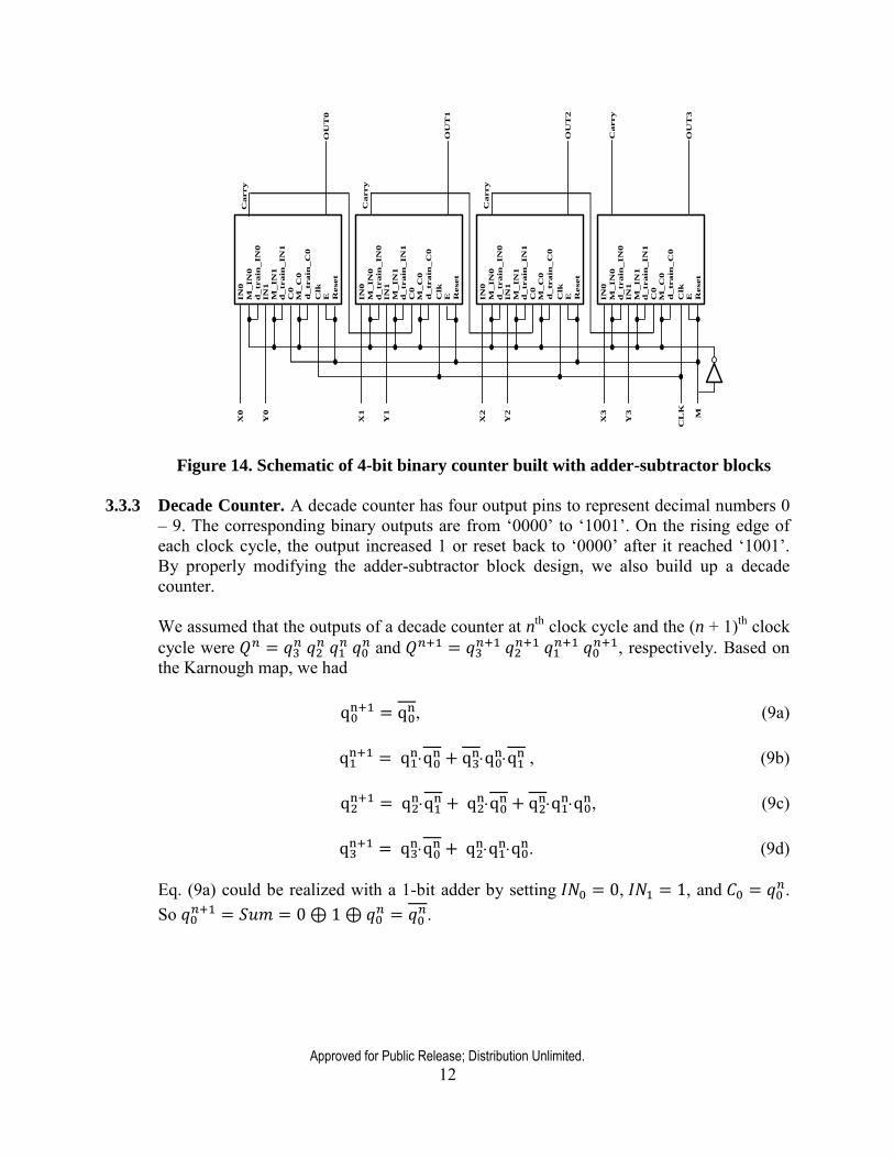
3.3.2 Binary Counter. An m-bit binary counter used n digital bits to represent 2m numbers. It incremented by 1 for every clock cycle and started over from 0 if all the digital bits were 1’s. We assumed the outputs of an m-bit binary counter at nth clock cycle and the (n + 1)th clock cycle were
and , respectively. Then we
had
( )
(8)
We used m-pieces of the above adder-subtractor blocks to build a binary counter. For ex-ample, Figure 14 shows a 4-bit counter based on the adder-subtractor blocks.
Approved for Public Release; Distribution Unlimited.
12
Reset
EClk
C0
M_
C0
d_
tra
in_
C0
IN
1
M_
IN
1d
_tra
in_
IN
1
IN
0
M_
IN
0
d_
tra
in_
IN
0
Reset
EClk
C0
M_
C0
d_
tra
in_
C0
IN
1
M_
IN
1d
_tra
in_
IN
1
IN
0
M_
IN
0
d_
tra
in_
IN
0
Reset
EClk
C0
M_
C0
d_
tra
in_
C0
IN
1
M_
IN
1d
_tra
in_
IN
1
IN
0
M_
IN
0
d_
tra
in_
IN
0
Reset
EClk
C0
M_
C0
d_
tra
in_
C0
IN
1
M_
IN
1d
_tra
in_
IN
1
IN
0
M_
IN
0
d_
tra
in_
IN
0
Ca
rry
Ca
rry
Ca
rry
OU
T1
OU
T2
OU
T0
OU
T3
M
CL
K
X0
Y0
X1
X2
X3
Y3
Y1
Y2
Ca
rry
Figure 14. Schematic of 4-bit binary counter built with adder-subtractor blocks
3.3.3 Decade Counter. A decade counter has four output pins to represent decimal numbers 0 – 9. The corresponding binary outputs are from ‘0000’ to ‘1001’. On the rising edge of each clock cycle, the output increased 1 or reset back to ‘0000’ after it reached ‘1001’. By properly modifying the adder-subtractor block design, we also build up a decade counter. We assumed that the outputs of a decade counter at nth clock cycle and the (n + 1)th clock cycle were and , respectively. Based on the Karnough map, we had
, (9a)
, (9b)
, (9c)
. (9d)
Eq. (9a) could be realized with a 1-bit adder by setting , , and . So
.
Approved for Public Release; Distribution Unlimited.
13
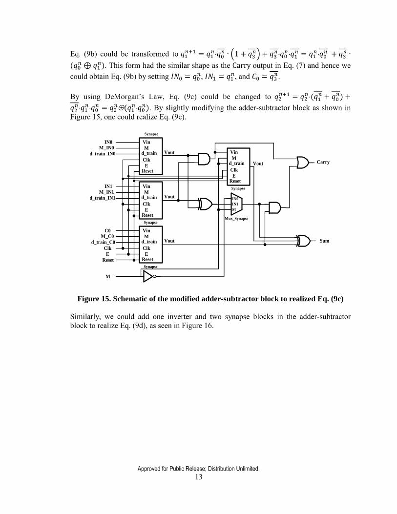
Eq. (9b) could be transformed to ( ) (
). This form had the similar shape as the output in Eq. (7) and hence we could obtain Eq. (9b) by setting , , and . By using DeMorgan’s Law, Eq. (9c) could be changed to ( )
(
). By slightly modifying the adder-subtractor block as shown in Figure 15, one could realize Eq. (9c).
Vin
Md_train
Clk
EReset
Vout
Vin
Md_train
Clk
EReset
Vout
Vin
Md_train
Clk
EReset
Vout
Reset
E
Clk
C0M_C0
d_train_C0
IN1M_IN1
d_train_IN1
IN0M_IN0
d_train_IN0
Carry
Sum
Synapse
Synapse
Synapse
M
IN0
IN1
M
Mux_Synapse
Vin
Md_train
Clk
EReset
Synapse
Vout
Figure 15. Schematic of the modified adder-subtractor block to realized Eq. (9c)
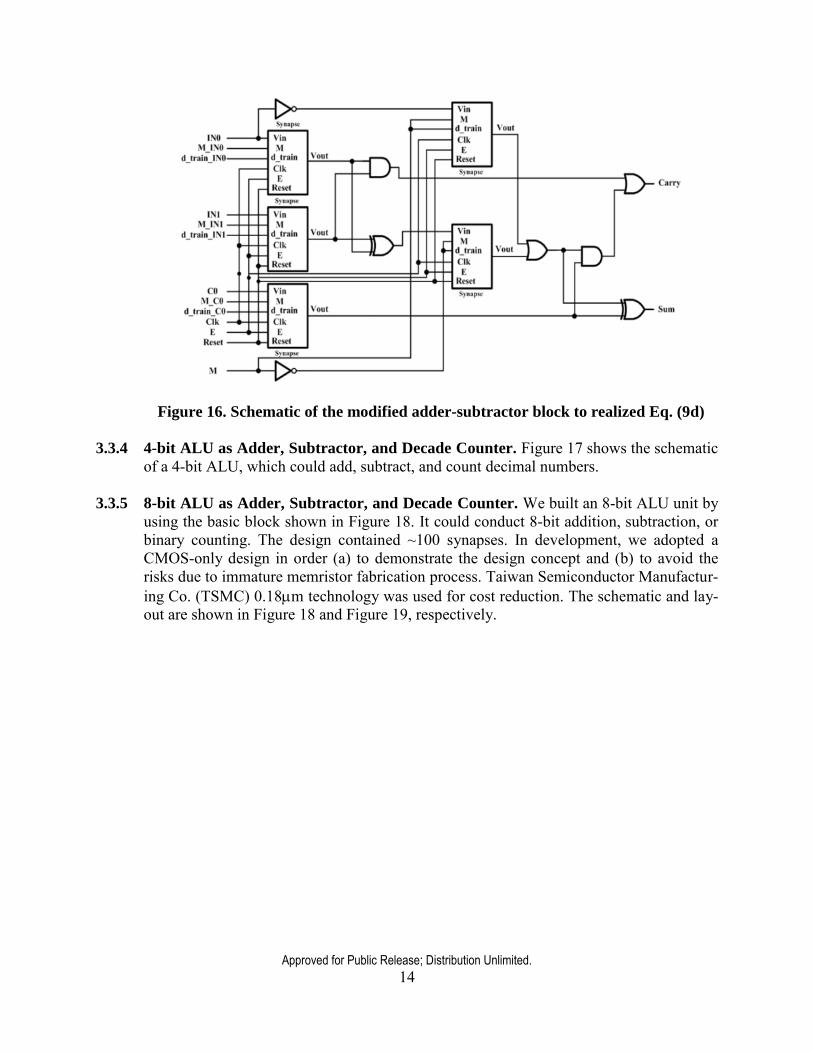
Similarly, we could add one inverter and two synapse blocks in the adder-subtractor block to realize Eq. (9d), as seen in Figure 16.
Approved for Public Release; Distribution Unlimited.
14
Figure 16. Schematic of the modified adder-subtractor block to realized Eq. (9d)
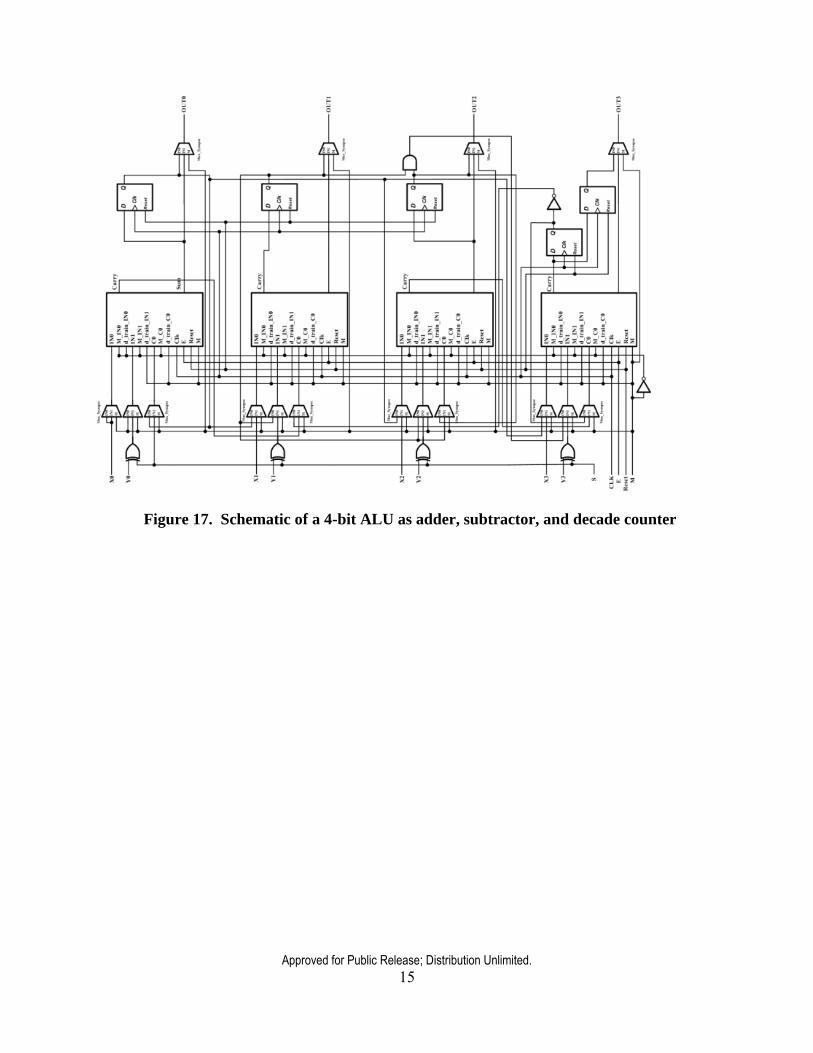
3.3.4 4-bit ALU as Adder, Subtractor, and Decade Counter. Figure 17 shows the schematic of a 4-bit ALU, which could add, subtract, and count decimal numbers.
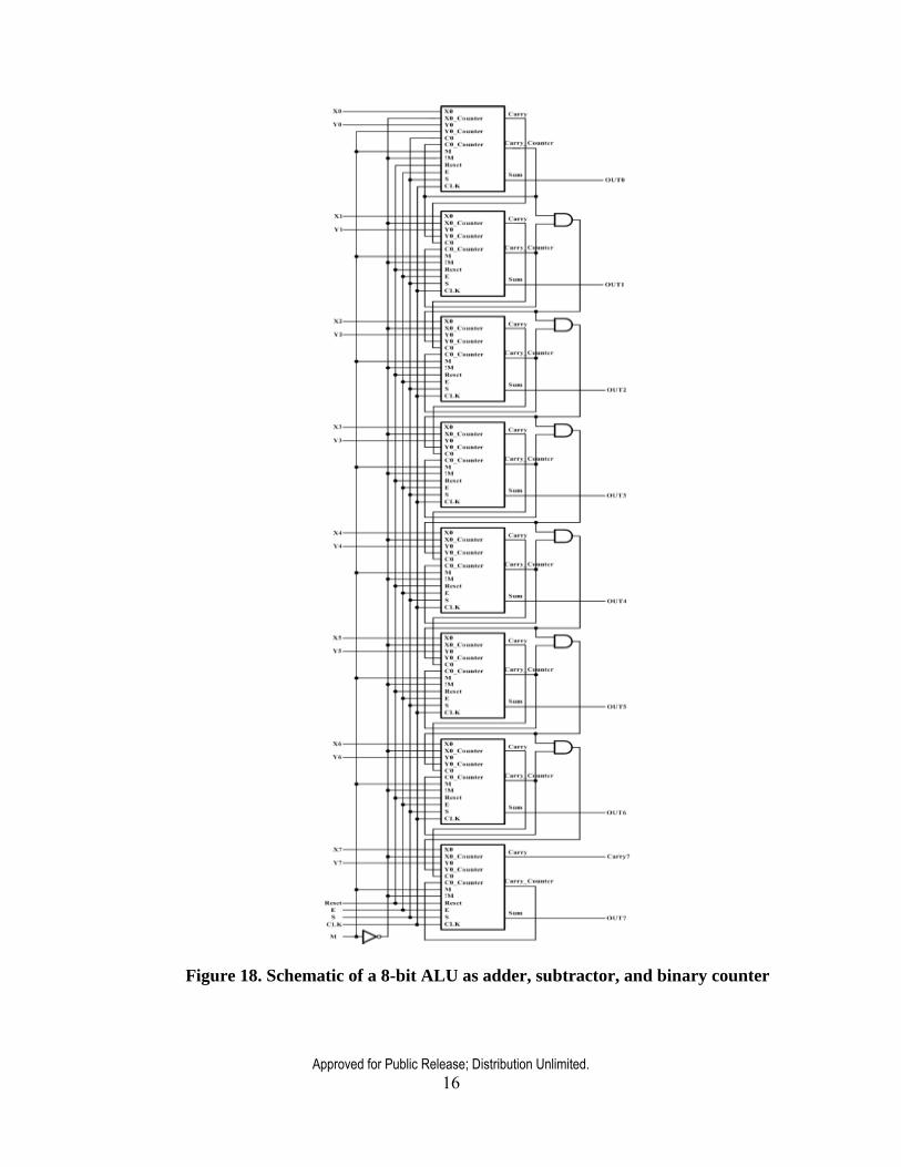
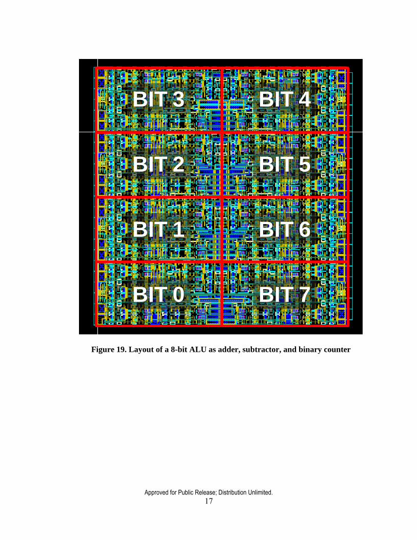
3.3.5 8-bit ALU as Adder, Subtractor, and Decade Counter. We built an 8-bit ALU unit by using the basic block shown in Figure 18. It could conduct 8-bit addition, subtraction, or binary counting. The design contained ~100 synapses. In development, we adopted a CMOS-only design in order (a) to demonstrate the design concept and (b) to avoid the risks due to immature memristor fabrication process. Taiwan Semiconductor Manufactur-ing Co. (TSMC) 0.18m technology was used for cost reduction. The schematic and lay-out are shown in Figure 18 and Figure 19, respectively.
Approved for Public Release; Distribution Unlimited.
15
Figure 17. Schematic of a 4-bit ALU as adder, subtractor, and decade counter
Approved for Public Release; Distribution Unlimited.
16
Figure 18. Schematic of a 8-bit ALU as adder, subtractor, and binary counter
Approved for Public Release; Distribution Unlimited.
17
Figure 19. Layout of a 8-bit ALU as adder, subtractor, and binary counter
BIT 0
BIT 1
BIT 2
BIT 3
BIT 7
BIT 6
BIT 5
BIT 4
Approved for Public Release; Distribution Unlimited.
18
4.0 RESULTS AND DISCUSSION
In the section, we will show the corresponding simulation results to validate the effec-tiveness of the proposed memristor-based synapsed based design. Also, the functionality of the ALU case study as an adder, subtractor, and binary counter will be verified.
4.1. Simulation Verification of Memristor-based Logic Design
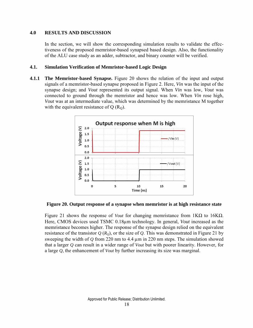
4.1.1 The Memristor-based Synapse. Figure 20 shows the relation of the input and output
signals of a memristor-based synapse proposed in Figure 2. Here, Vin was the input of the synapse design; and Vout represented its output signal. When Vin was low, Vout was connected to ground through the memristor and hence was low. When Vin rose high, Vout was at an intermediate value, which was determined by the memristance M together with the equivalent resistance of Q (RQ).
Figure 20. Output response of a synapse when memristor is at high resistance state
Figure 21 shows the response of Vout for changing memristance from 1KΩ to 16KΩ. Here, CMOS devices used TSMC 0.18m technology. In general, Vout increased as the memristance becomes higher. The response of the synapse design relied on the equivalent resistance of the transistor Q (RQ), or the size of Q. This was demonstrated in Figure 21 by sweeping the width of Q from 220 nm to 4.4 m in 220 nm steps. The simulation showed that a larger Q can result in a wider range of Vout but with poorer linearity. However, for a large Q, the enhancement of Vout by further increasing its size was marginal.
Approved for Public Release; Distribution Unlimited.
19
Figure 21. Output voltage of a memristor-based synapse vs. memristance
To improve design stability, a buffer can be added at the output of the synapse to increase the voltage swing. Furthermore, some circuit optimization techniques, such as an asym-metry gate in other blocks, could be used to minimize the overall synapse-based system.
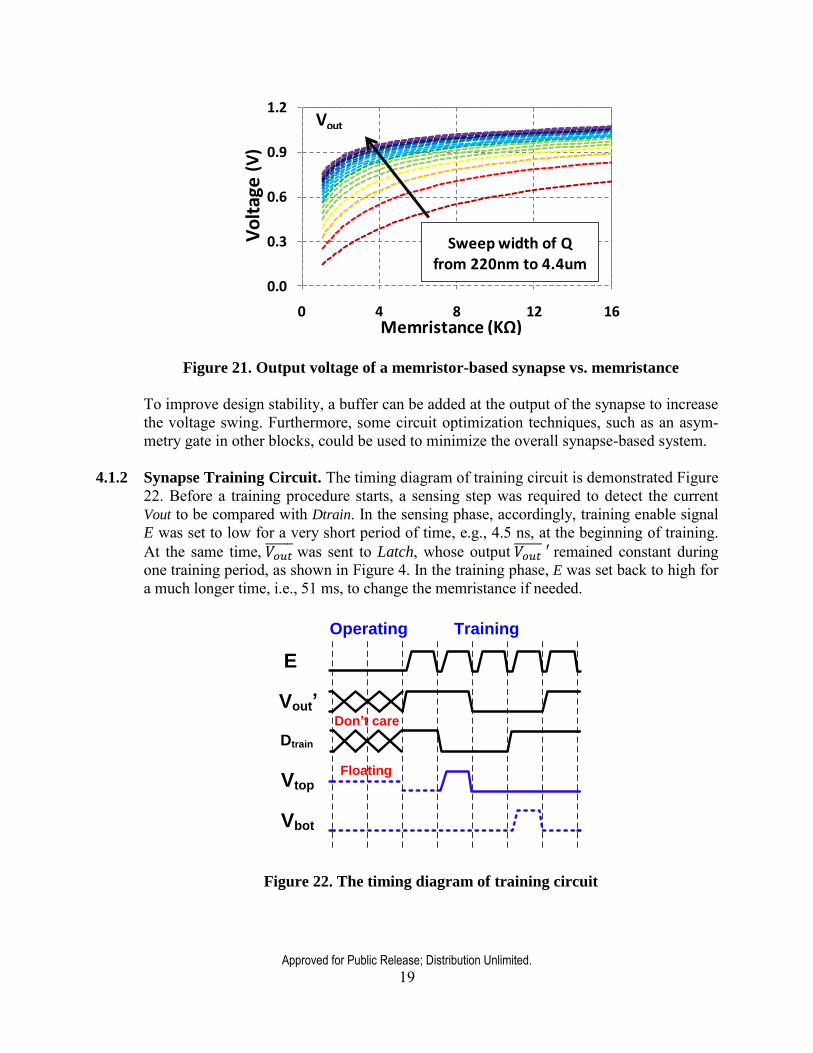
4.1.2 Synapse Training Circuit. The timing diagram of training circuit is demonstrated Figure 22. Before a training procedure starts, a sensing step was required to detect the current Vout to be compared with Dtrain. In the sensing phase, accordingly, training enable signal E was set to low for a very short period of time, e.g., 4.5 ns, at the beginning of training. At the same time, was sent to Latch, whose output remained constant during one training period, as shown in Figure 4. In the training phase, E was set back to high for a much longer time, i.e., 51 ms, to change the memristance if needed.
Figure 22. The timing diagram of training circuit
0.0
0.3
0.6
0.9
1.2
0 4 8 12 16Memristance (KΩ)
Vout
Vo
ltag
e(V
)Sweep width of Q
from 220nm to 4.4um
Dtrain
E
Vout’
Vtop
Vbot
Floating
Operating Training
Don’t care
Approved for Public Release; Distribution Unlimited.
20
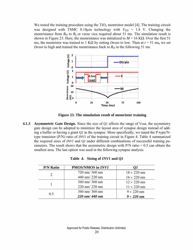
We tested the training procedure using the TiO2 memristor model [4]. The training circuit was designed with TSMC 0.18m technology with VDD = 1.8 V. Changing the memristance from RH to RL or verse vice required about 51 ms. The simulation result is shown in Figure 23. Here, the memristance was initialized to M = 16 KΩ. Over the first 51 ms, the memristor was trained to 1 KΩ by setting Dtrain to low. Then at t = 51 ms, we set Dtrain to high and trained the memristance back to RH in the following 51 ms.
Figure 23. The simulation result of memristor training
4.1.3 Asymmetric Gate Design. Since the size of Q1 affects the range of Vout, the asymmetry
gate design can be adopted to minimize the layout area of synapse design instead of add-ing a buffer or having a giant Q1 in the synapse. More specifically, we tuned the P-type/N-type transistor (P/N) ratio of INV1 of the training circuit in Figure 4. Table 4 summarized the required sizes of INV1 and Q1 under different combinations of successful training pa-rameters. The result shows that the asymmetric design with P/N ratio = 0.5 can obtain the smallest area. The last option was used in the following synapse analysis.
Table 4. Sizing of INV1 and Q1
P/N Ratio PMOS/NMOS in INV1 Q1
2 720 nm/ 360 nm 18 220 nm 440 nm/ 220 nm 16 220 nm
1 360 nm/ 360 nm 12 220 nm 220 nm/ 220 nm 11 220 nm
0.5 360 nm/ 360 nm 9 220 nm 220 nm/ 440 nm 9 220 nm
0
1
2
0 25 50 75 100
Vo
ltag
e (V
)
Dtrain
0
1
2
0 25 50 75 100
Vo
ltag
e (V
)
E
0
10
20
0 25 50 75 100
Me
mri
stan
ce
(KΩ
)
M
Time (ms)
4.5ns
read
Approved for Public Release; Distribution Unlimited.
21
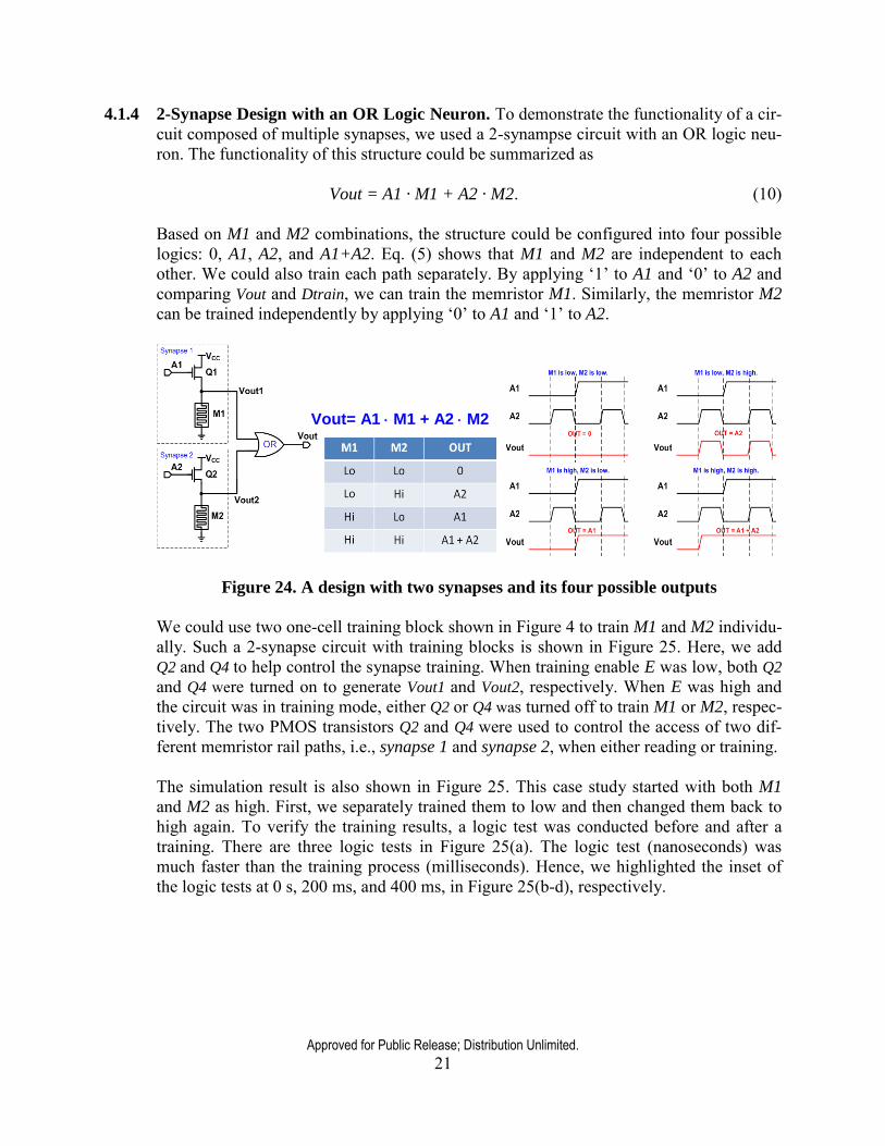
4.1.4 2-Synapse Design with an OR Logic Neuron. To demonstrate the functionality of a cir-cuit composed of multiple synapses, we used a 2-synampse circuit with an OR logic neu-ron. The functionality of this structure could be summarized as
Vout = A1 · M1 + A2 · M2. (10)
Based on M1 and M2 combinations, the structure could be configured into four possible logics: 0, A1, A2, and A1+A2. Eq. (5) shows that M1 and M2 are independent to each other. We could also train each path separately. By applying ‘1’ to A1 and ‘0’ to A2 and comparing Vout and Dtrain, we can train the memristor M1. Similarly, the memristor M2 can be trained independently by applying ‘0’ to A1 and ‘1’ to A2.
Figure 24. A design with two synapses and its four possible outputs
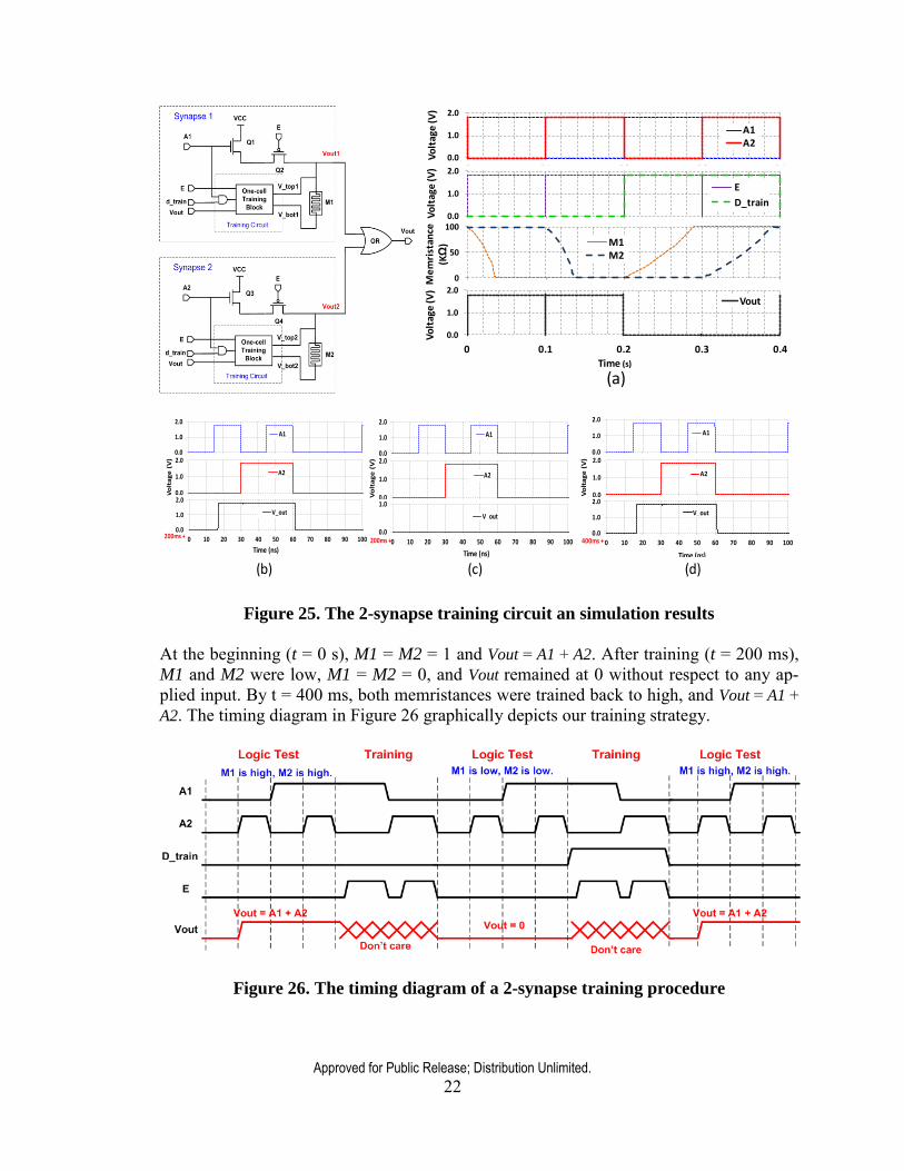
We could use two one-cell training block shown in Figure 4 to train M1 and M2 individu-ally. Such a 2-synapse circuit with training blocks is shown in Figure 25. Here, we add Q2 and Q4 to help control the synapse training. When training enable E was low, both Q2 and Q4 were turned on to generate Vout1 and Vout2, respectively. When E was high and the circuit was in training mode, either Q2 or Q4 was turned off to train M1 or M2, respec-tively. The two PMOS transistors Q2 and Q4 were used to control the access of two dif-ferent memristor rail paths, i.e., synapse 1 and synapse 2, when either reading or training. The simulation result is also shown in Figure 25. This case study started with both M1 and M2 as high. First, we separately trained them to low and then changed them back to high again. To verify the training results, a logic test was conducted before and after a training. There are three logic tests in Figure 25(a). The logic test (nanoseconds) was much faster than the training process (milliseconds). Hence, we highlighted the inset of the logic tests at 0 s, 200 ms, and 400 ms, in Figure 25(b-d), respectively.
Vout= A1 M1 + A2 M2
Approved for Public Release; Distribution Unlimited.
22
Figure 25. The 2-synapse training circuit an simulation results
At the beginning (t = 0 s), M1 = M2 = 1 and Vout = A1 + A2. After training (t = 200 ms), M1 and M2 were low, M1 = M2 = 0, and Vout remained at 0 without respect to any ap-plied input. By t = 400 ms, both memristances were trained back to high, and Vout = A1 + A2. The timing diagram in Figure 26 graphically depicts our training strategy.
Figure 26. The timing diagram of a 2-synapse training procedure
0.0
1.0
2.0
0 0.1 0.2 0.3 0.4
Vo
ltag
e (V
)
A1A2
0.0
1.0
2.0
0 0.1 0.2 0.3 0.4
Vo
ltag
e (V
)
E
D_train
0
50
100
0 0.1 0.2 0.3 0.4
Me
mri
stan
ce
(KΩ
) M1M2
0.0
1.0
2.0
0 0.1 0.2 0.3 0.4
Vo
ltag
e (V
)
Vout
Time (s)
(a)
0.0
1.0
2.0
0 10 20 30 40 50 60 70 80 90 100
A1
0.0
1.0
2.0
0 10 20 30 40 50 60 70 80 90 100
Vo
lta
ge
(V
)
A2
0.0
1.0
2.0
0 10 20 30 40 50 60 70 80 90 100
V_out
200ms +
Time (ns)
0.0
1.0
2.0
0 10 20 30 40 50 60 70 80 90 100
A1
Time (ns)
0.0
1.0
2.0
0 10 20 30 40 50 60 70 80 90 100
Vo
lta
ge
(V
)
A2
0.0
1.0
0 10 20 30 40 50 60 70 80 90 100
V_out
200ms +
0.0
1.0
2.0
0 10 20 30 40 50 60 70 80 90 100
A1
Time (ns)
0.0
1.0
2.0
0 10 20 30 40 50 60 70 80 90 100
Vo
lta
ge
(V
)
A2
0.0
1.0
2.0
0 10 20 30 40 50 60 70 80 90 100
V_out
400ms +
(b) (c) (d)
Approved for Public Release; Distribution Unlimited.
23
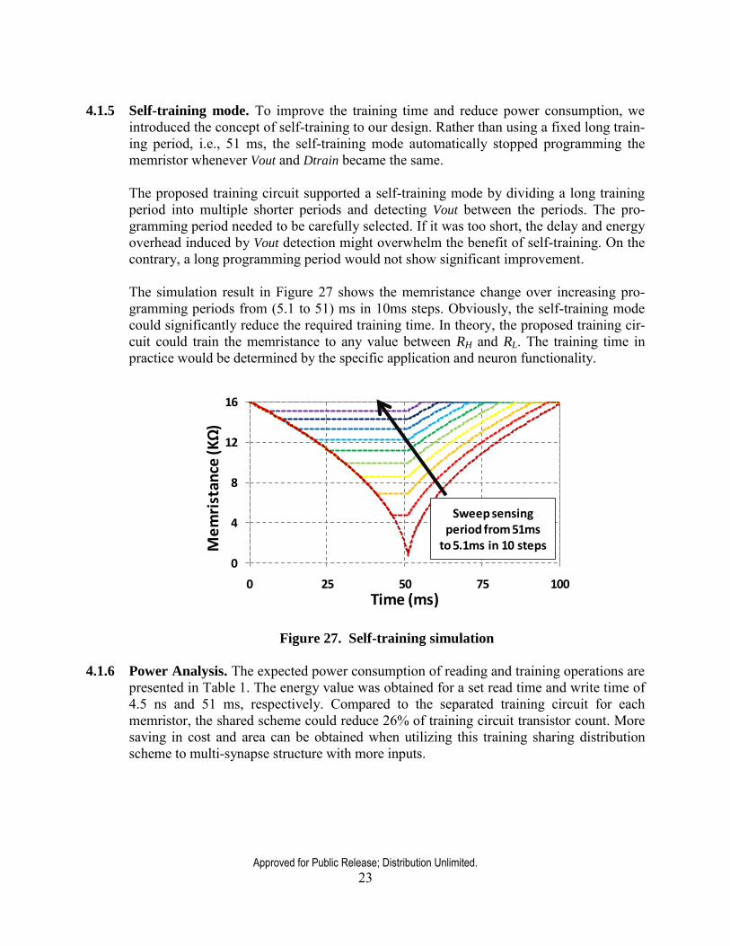
4.1.5 Self-training mode. To improve the training time and reduce power consumption, we
introduced the concept of self-training to our design. Rather than using a fixed long train-ing period, i.e., 51 ms, the self-training mode automatically stopped programming the memristor whenever Vout and Dtrain became the same. The proposed training circuit supported a self-training mode by dividing a long training period into multiple shorter periods and detecting Vout between the periods. The pro-gramming period needed to be carefully selected. If it was too short, the delay and energy overhead induced by Vout detection might overwhelm the benefit of self-training. On the contrary, a long programming period would not show significant improvement. The simulation result in Figure 27 shows the memristance change over increasing pro-gramming periods from (5.1 to 51) ms in 10ms steps. Obviously, the self-training mode could significantly reduce the required training time. In theory, the proposed training cir-cuit could train the memristance to any value between RH and RL. The training time in practice would be determined by the specific application and neuron functionality.
Figure 27. Self-training simulation
4.1.6 Power Analysis. The expected power consumption of reading and training operations are
presented in Table 1. The energy value was obtained for a set read time and write time of 4.5 ns and 51 ms, respectively. Compared to the separated training circuit for each memristor, the shared scheme could reduce 26% of training circuit transistor count. More saving in cost and area can be obtained when utilizing this training sharing distribution scheme to multi-synapse structure with more inputs.
0
4
8
12
16
0 25 50 75 100
Me
mri
stan
ce (
KΩ
)
Sweep sensing period from 51ms
to 5.1ms in 10 steps
Time (ms)
Approved for Public Release; Distribution Unlimited.
24
Table 5. Synapse Power Consumption Analysis
Operation Power Energy
Read RL 1.04 mW 4.68 pJ RH 113.4 uW 0.51 pJ
Training From RH to RL 216.7 uW 11.1 uJ From RL to RH 234 uW 11.9 uJ
4.2. The Functionality Verification of 8-bit ALU Design
In this section, we will demonstrate addition, subtraction, and counting functionalities of the proposed synapse-based ALU design. Though our simulations proved the functionali-ty of the ALU design, it is impractical to graphically present all possible input combina-tions. Only a few representative input combinations are presented.
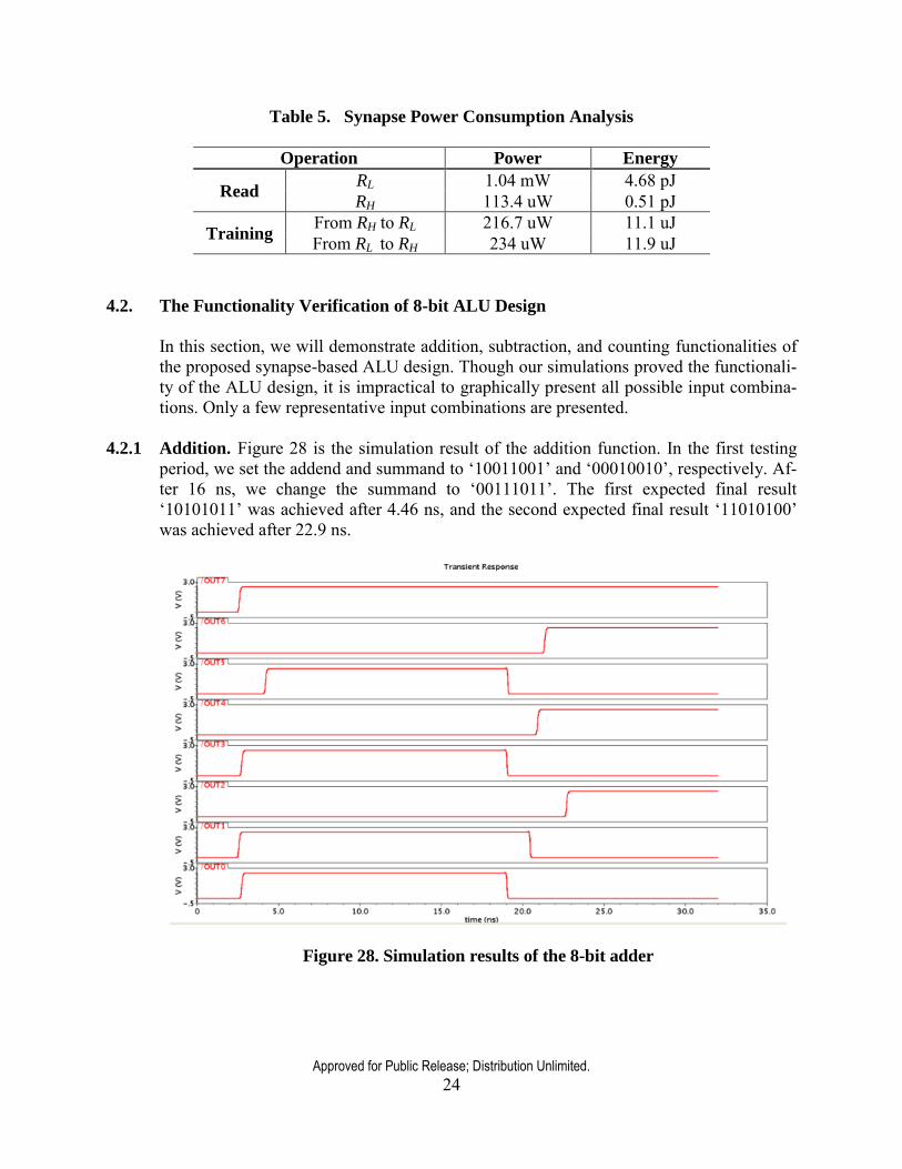
4.2.1 Addition. Figure 28 is the simulation result of the addition function. In the first testing period, we set the addend and summand to ‘10011001’ and ‘00010010’, respectively. Af-ter 16 ns, we change the summand to ‘00111011’. The first expected final result ‘10101011’ was achieved after 4.46 ns, and the second expected final result ‘11010100’ was achieved after 22.9 ns.
Figure 28. Simulation results of the 8-bit adder
Approved for Public Release; Distribution Unlimited.
25
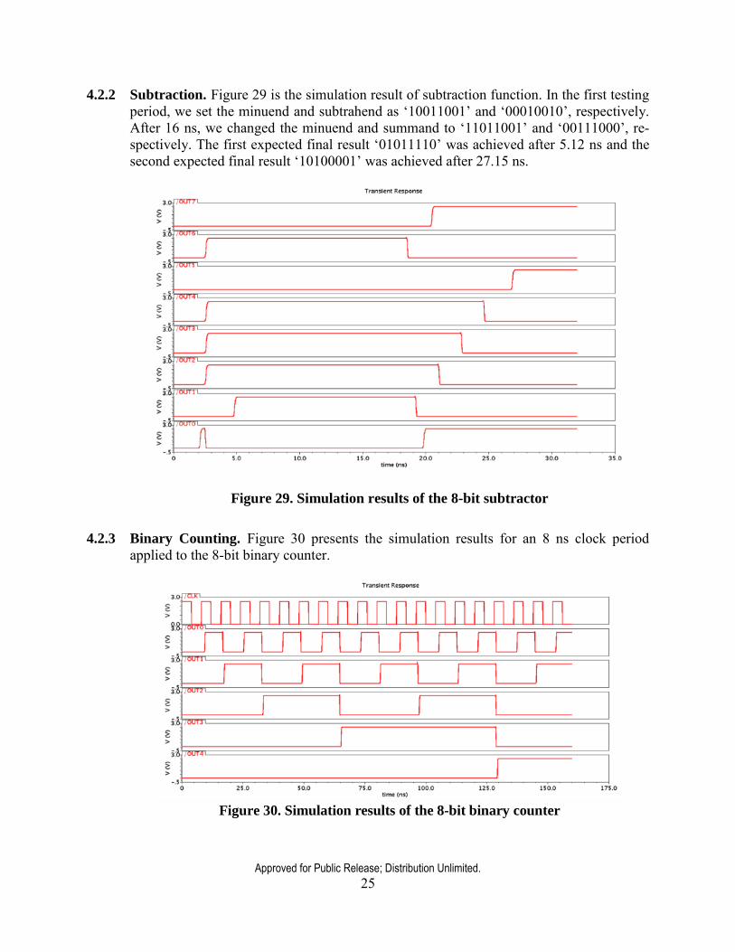
4.2.2 Subtraction. Figure 29 is the simulation result of subtraction function. In the first testing period, we set the minuend and subtrahend as ‘10011001’ and ‘00010010’, respectively. After 16 ns, we changed the minuend and summand to ‘11011001’ and ‘00111000’, re-spectively. The first expected final result ‘01011110’ was achieved after 5.12 ns and the second expected final result ‘10100001’ was achieved after 27.15 ns.
Figure 29. Simulation results of the 8-bit subtractor
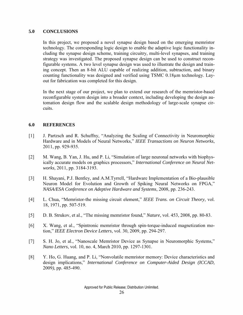
4.2.3 Binary Counting. Figure 30 presents the simulation results for an 8 ns clock period
applied to the 8-bit binary counter.
Figure 30. Simulation results of the 8-bit binary counter
Approved for Public Release; Distribution Unlimited.
26
5.0 CONCLUSIONS
In this project, we proposed a novel synapse design based on the emerging memristor technology. The corresponding logic design to enable the adaptive logic functionality in-cluding the synapse design scheme, training circuitry, multi-level synapses, and training strategy was investigated. The proposed synapse design can be used to construct recon-figurable systems. A two level synapse design was used to illustrate the design and train-ing concept. Then an 8-bit ALU capable of realizing addition, subtraction, and binary counting functionality was designed and verified using TSMC 0.18µm technology. Lay-out for fabrication was completed for this design. In the next stage of our project, we plan to extend our research of the memristor-based reconfigurable system design into a broader context, including developing the design au-tomation design flow and the scalable design methodology of large-scale synapse cir-cuits.
6.0 REFERENCES
[1] J. Partzsch and R. Schuffny, “Analyzing the Scaling of Connectivity in Neuromorphic
Hardware and in Models of Neural Networks,” IEEE Transactions on Neuron Networks, 2011, pp. 929-935.
[2] M. Wang, B. Yan, J. Hu, and P. Li, “Simulation of large neuronal networks with biophys-ically accurate models on graphics processors,” International Conference on Neural Net-
works, 2011, pp. 3184-3193.
[3] H. Shayani, P.J. Bentley, and A.M.Tyrrell, “Hardware Implementation of a Bio-plausible Neuron Model for Evolution and Growth of Spiking Neural Networks on FPGA,” NASA/ESA Conference on Adeptive Hardware and Systems, 2008, pp. 236-243.
[4] L. Chua, “Memristor-the missing circuit element,” IEEE Trans. on Circuit Theory, vol. 18, 1971, pp. 507-519.
[5] D. B. Strukov, et al., “The missing memristor found,” Nature, vol. 453, 2008, pp. 80-83.
[6] X. Wang, et al., “Spintronic memristor through spin-torque-induced magnetization mo-tion,” IEEE Electron Device Letters, vol. 30, 2009, pp. 294-297.
[7] S. H. Jo, et al., “Nanoscale Memristor Device as Synapse in Neuromorphic Systems,” Nano Letters, vol. 10, no. 4, March 2010, pp. 1297-1301.
[8] Y. Ho, G. Huang, and P. Li, “Nonvolatile memristor memory: Device characteristics and design implications,” International Conference on Computer-Aided Design (ICCAD, 2009), pp. 485-490.
Approved for Public Release; Distribution Unlimited.
27
[9] J. Cong and B. Xiao, “mrFPGA: A novel FPGA architecture with memristor-based re-configuration,” International Symposium on Nanoscale Architectures, 2011, pp. 1-8.
[10] J. Rajendran, H. Manem, R. Karri, and G. Rose, “Memristor based programmable thresh-old logic array,” IEEE/ACM International Symposium on Nanoscale Architecture, Jun. 2010, pp. 5–10.
[11] G. Rose, R. Pino, and Q. Wu, “Exploiting Memristance for Low-Energy Neuromorphic Computing Hardware,” IEEE International Symposium on Circuits and Systems (ISCAS), 2011, pp. 2942-2945.
[12] V. Erokhin and M. P. Fontana, “Electrochemically controlled polymeric device: a memristor (and more) found two years ago,” 2008.
[13] J. H. Kriegerand and S. M. Spitzer, “Non-traditional, non-volatile memory based on switching and retention phenomena in polymeric thin films,” Non-Volatile Memory
Technology Symposium, 2004, pp. 121-124.
[14] Y. Huai, “Spin-Transfer Torque MRAM (STT-MRAM): Challenges and Prospects,” AAPPS Bulletin, vol. 18, December 2008, pp. 33.
[15] P. Krzysteczko, G. Reiss, and A. Thomas, “Memristive switching of MgO based magnetic tunnel junctions,” Applied Physics Letters, vol. 95, 2009, pp. 112508-3.
[16] K. K. Gullapalli, A. J. Tsao, and D. P. Neikirk, “Multiple self-consistent solutions at zero bias and multiple conduction curves in quantum tunneling diodes incorporating N--N+-N- spacer layers,” Applied Physics Letters, vol. 62, 1993, pp. 2971-2973.
[17] D. Strukov, J. Borghetti, and S. Williams, “Coupled ionic and electronic transport model of thin-film semiconductor memristive behavior,” Small, vol. 5, 2009, pp. 1058-1063.
[18] Webwire, “Memristor could Enable Memory Chip Computation,” [Online], Available: http://www.webwire.com/ViewPressRel.asp?aId=115179 [Accessed: April 9, 2010]
[19] Y. V. Pershin, et al., “Experimental demonstration of associative memory with memris-tive neural networks,” Nature Proceedings, 2009.
[20] H. Choi, et al., “An electrically modifiable synapse array of resistive switching memory,” Nanotechnology, vol. 20, 2009, pp. 345201.
Approved for Public Release; Distribution Unlimited.
28
APPENDIX A - Publications and Presentations
1. H. Li and R. E. Pino, Statistical Memristor Model and Its Applications in Neuromorphic
Computing, a book chapter in Advances in Neuromorphic Memristor Science and Applica-
tions, edited by R. Kozma, R. E. Pino, and G. Pazienza, Springer, 2012.
2. Y.-C. Chen, H. Li, W. Zhang, and R. Pino, “3-Dimensional High-Density Interleaved Memory for Bipolar RRAM Design,” to appear in IEEE Transaction on Nanotechnology.
3. H. Li, R. Pino, Y. Chen, M. Hu, and B. Liu, “Statistical Memristor Modeling and Case Study in Neuromorphic Computing,” Design Automation Conference (DAC), June 2012, pp. 585-590.
4. H. Wang, H. Li, and R. E. Pino, “Memristor-based Synapse Design and Training Scheme for Neuromorphic Computing Architecture,” International Joint Conference on Neural Networks
(IJCNN), June 2012.
5. X. Bi, C. Zhang, H. Li, Y. Chen, and R. Pino, “Spintronic Memristor Based Temperature
Sensor De-sign with CMOS Current Reference,” Design, Automation & Test in Europe
(DATE), Dresden, Germany, March 2012, pp. 1301-1306.
6. M. Hu, H. Li, and R. E. Pino, “Statistical Model of TiO2 Memristor and Applications,” Inter-
national Conference on Computer Aided Design (ICCAD), November 2011, pp. 345-352.
7. Y.C. Chen, H. Li, W. Zhang, and R. Pino, “3D-HIM: A 3-Dimensional High-Density Inter-leaved Memory for Bipolar RRAM Design,” IEEE/ACM International Symposium on Na-
noscale Architectures (NANOARCH), June 2011, pp. 59-64.
8. Y.C. Chen, H. Li, Y. Chen, and R. Pino, “3D-ICML: A 3D Bipolar ReRAM Design with In-terleaved Complementary Memory,” Design, Automation & Test in Europe Conference and
Exhibition (DATE), March 2011, pp. 1-4.
9. M. Hu, H. Li, Y. Chen, X. Wang, and R. E. Pino, “Geometry Variations Analysis of TiO2–based and Spintronic Memristors,” the 16th Asia and South Pacific Design Automation Con-
ference (ASPDAC), Jan. 2011, pp. 25-30. (Best Paper Nomination, 1 out of 28 in track,
3.6%)
10. M. Hu, H. Li, Y. Chen, and R. E. Pino, “Statistical Model of TiO2 Memristor,” the 48th De-
sign Automation Conference (DAC), in WIP track, June 2011.

Approved for Public Release; Distribution Unlimited.
29
LIST OF ABBREVIATIONS AND ACRONYMS ALU arbitrary logic unit P/N P-type/N-type transistor TSMC Taiwan Semiconductor Manufacturing Co.