Embed Size (px)
Citation preview
MEMORY SYSTEM DESIGN: INTEGRATION OF CACHES,
TRANSLATION LOOKASIDE BUFFERS (TLB) AND SDRAM
BY
CHING LI-LYNN
A REPORT
SUBMITTED TO
Universiti Tunku Abdul Rahman
in partial fulfillment of the requirements
for the degree of
BACHELOR OF INFORMATION TECHNOLOGY (HONS)
COMPUTER ENGINEERING
Faculty of Information and Communication Technology
(Perak Campus)
AUGUST 2013

BIT (Hons) Computer Engineering
Faculty of Information and Communication Technology (Perak Campus), UTAR ii

BIT (Hons) Computer Engineering
Faculty of Information and Communication Technology (Perak Campus), UTAR iii
DECLARATION OF ORIGINALITY
I declare that this report entitled “MEMORY SYSTEM DESIGN: INTEGRATION
OF CACHES, TRANSLATION LOOKASIDE BUFFERS (TLB) AND SDRAM”
is my own work except as cited in the references. The report has not been accepted for
any degree and is not being submitted concurrently in candidature for any degree or
other award.
Signature : _________________________
Name : _________________________
Date : _________________________

BIT (Hons) Computer Engineering
Faculty of Information and Communication Technology (Perak Campus), UTAR iv
Acknowledgement
Thank you everybody! Words just can‟t express my gratitude.

BIT (Hons) Computer Engineering
Faculty of Information and Communication Technology (Perak Campus), UTAR v
Abstract
This project is to enhance the current RISC32 architecture that developed in
Universiti Tunku Abdul Rahman under Faculty of Information and Communication
Technology. After reviewing the previous work, the RISC32 processor has a working
SDRAM controller and SDRAM, but its Cache and Translation Lookaside Buffer
(TLB) are not working quite well.
Hence, this project is initiated to integrate these parts together as a whole
Memory System. The Cache and TLB are not behaved as expected. The Cache will
send one time more address to the SDRAM, which might cause data loss. Other than
that, the TLB also has some problem. All of these need to be fixed to that they can be
integrated together as a Memory System. This project is modelled using Verilog HDL.
BIT (Hons) Computer Engineering
Faculty of Information and Communication Technology (Perak Campus), UTAR vi
Table of Contents
Title i
Declaration of Originality iii
Acknowledgement iv
Abstract v
Table of Contents vi
List of Figures x
List of Tables xii
Chapter 1: Introduction 1
1.1 Background 1
1.2 Problem Statement and Motivation 2
1.3 Project Objectives 4
Chapter 2: Literature Review 5
2.1 MIPS – a RISC Processor 5
2.2 Memory Hierarchy 5
2.3 DRAM 6
2.4 SDRAM 7

BIT (Hons) Computer Engineering
Faculty of Information and Communication Technology (Perak Campus), UTAR vii
2.5 SDRAM Controller 13
2.6 Cache 29
2.7 Translation Lookaside Buffer (TLB) 39
Chapter 3: Methodology and Development Tools 49
3.1 Methodology 49
3.2 Design Tools 52
Chpater 4: Architecture of the RISC32 55
4.1 Design Hierachy 56
Chapter 5: Memory System Design 57
5.1 Memory System Specifications 57
5.2 Naming Convention 57
5.3 Memory Map 59
5.4 Memory System Interface 61
5.5 Memory System Operating Procedure 68

BIT (Hons) Computer Engineering
Faculty of Information and Communication Technology (Perak Campus), UTAR viii
Chapter 6: Micro-architecture Specification 69
6.1 Unit Partitioning of Memory System 69
6.2 Cache Unit 70
6.2.1 I/O Description 71
6.2.2 Block Partitioning of Cache Unit 75
6.2.3 Cache Controller Block 76
6.2.4 Cache Datapath Block 82
6.3 Translation Lookaside Buffer (TLB) Unit 88
6.3.1 I/O Description 89
6.3.2 Block Partitioning of TLB Unit 94
6.3.3 Memory Management Unit (MMU) block 95
6.3.4 TLB Datapath Block 100
6.4 Memory Arbiter Block 104
6.5 CP0 Multiplexer Block 109
Chapter 7: Test and Verification 115
7.1 Test Plan 115

BIT (Hons) Computer Engineering
Faculty of Information and Communication Technology (Perak Campus), UTAR ix
7.2 Test Bench 116
7.3 Simulation Results 122
Chapter 8: Discussion and Conclusion 131
8.1 Discussion and Conclusion 131
8.2 Future Works 132
References 133

BIT (Hons) Computer Engineering
Faculty of Information and Communication Technology (Perak Campus), UTAR x
List of Figures
Figure Number Title Page
Figure 2.2.1 The Memory Hierarchy 6
Figure 2.3.1 Structures of DRAM and SRAM 7
Figure 2.4.1 Block diagram of MT48LC4M32B2 8
Figure 2.4.2 A simplified view on how the SDRAM arrays are
addressed
9
Figure 2.4.3 Mode Register definition
11
Figure 2.5.1 Block diagram of SDRAM Controller 13
Figure 2.5.2 The Microarchitecture of SDRAM Controller. 15
Figure 2.5.3 Protocol Controller Block FSM 17
Figure 2.5.4 The protocol follows the SDRAM initialisation
requirement as instructed by MICRON
22
Figure 2.5.5 Keep Bank and Row Open Access Protocol to
achieve fast access cycle for same row access
23
Figure 2.5.6 Load Mode Protocol 24
Figure 2.5.7 Auto Refresh Protocol 25
Figure 2.5.8 Read Protocol 26
Figure 2.5.9 Write Protocol 27
Figure 2.6.1 Cache Unit designed by Khoo Chong Siang 29
Figure 2.6.2 Read Protocol of Cache 33
Figure 2.6.3 Write Protocol of Cache 34
Figure 2.6.4 Read Hit 35
Figure 2.6.5 Read Miss 36
Figure 2.6.6 Write Miss 37
Figure 2.6.7 Write Hit 38
Figure 2.7.1 Virtual Memory Map based on 32-bits MIPS 39
Figure 2.7.2 An example of address translation 40
Figure 2.7.3 An overall picture of how virtual memory works. 41
Figure 2.7.4 An example of how an 8-block cache configures
as direct mapped, two-way set assoiciative, four-
way set associative and fully associative cache.
42
Figure 2.7.5 Contents of a TLB entry 42
Figure 2.7.6 Usage of TLB in address translation by using 48
entries and fully associative TLB.
43

BIT (Hons) Computer Engineering
Faculty of Information and Communication Technology (Perak Campus), UTAR xi
Figure 2.7.7 The design of physically addressed cache.
44
Figure 2.7.8 The design of virtually addressed cache. 44
Figure 2.7.9 Current design of TLB by Kim Yuh Chang 45
Figure 2.7.10 Current design of MMU by Kim Yuh Chang 46
Figure 2.7.11 Segmentation of virtual address of current design 47
Figure 2.7.12 The usage of 2-level page table in address
translation
48
Figure 3.1.1 General Design Flow without Synthesis and
Physical Design
50
Figure 4.0.1 Full RISC32‟s Architecture and Micro-
architecture Partitioning.
55
Figure 5.4.0.1 Block Diagram of u_mem_sys 61
Figure 6.1.1 Micro-architecture of the Memory System 69
Figure 6.2.0.1 Block diagram of u_cache 70
Figure 6.2.2.1 Block Partition of Cache Unit 75
Figure 6.2.3.1 Block diagram of b_cache_ctrl 76
Figure 6.2.4.1 Block diagram of b_cache_dp 82
Figure 6.3.0.1 Block digram of u_tlb 88
Figure 6.3.2.1 Block partitioning of TLB Unit 94
Figure 6.3.3.1 Block diagram of b_mmu 95
Figure 6.3.4.1 Block diagram of b_tlb_dp 100
Figure 6.4.0.1 Block diagram of b_mem_arbiter 104
Figure 6.5.0.1 Block diagram of b_cp0_mux 109
Figure 7.1.1 Test plan for Memory System 115
Figure 7.3.1 Simulation results 122
Figure 7.3.2 Simulation results 123
Figure 7.3.3 Simulation results 124
Figure 7.3.4 Simulation results 125
Figure 7.3.5 Simulation results 126
Figure 7.3.6 Simulation results 127
Figure 7.3.7 Simulation results 128
Figure 7.3.8 Simulation results 129
Figure 7.3.9 SRAM‟s read/write transcript 130

BIT (Hons) Computer Engineering
Faculty of Information and Communication Technology (Perak Campus), UTAR xii
List of Tables
Table Number Title Page
Table 2.4.1 List of SDRAM commands and their respective
function
10
Table 2.5.1 I/O pin description of SDRAM Controller. 13
Table 2.5.2 State definition of Protocol Controller 18
Table 2.5.3 Branch conditions of Protocol Controller 18
Table 2.5.4 Outputs of the states of Protocol Controller 19
Table 3.1 Comparison between „Big 3‟ Simulators 53
Table 4.1.1 Formation of a design hierarchy for Full RISC32
microprocessor through top down design
methodology
56
Table 5.1.1 Specifications of the Memory System 57
Table 5.2.1 Naming convention 58
Table 5.3.1 Virtual memory map of 32-bits MIPS 59
Table 5.4.1.1.1 Memory System‟s input pin description. 62
Table 5.4.1.2.1 Memory System‟s output pin description 64
Table 6.2.1.1.1 Cache Unit‟s input pin description 71
Table 6.2.1.2.1 Cache Unit‟s output pin description 73
Table 6.2.3.1.1.1 Cache Controller‟s input pin description 77
Table 6.2.3.1.2.1 Cache Controller‟s output pin description 79
Table 6.2.4.1.1.1 Cache Datapath‟s input pin description 83
Table 6.2.4.1.2.1 Cache Datapath‟s output pin description 86
Table 6.3.1.1.1 TLB Unit‟s input pin description 89
Table 6.3.1.2.1 TLB Unit‟s output pin description 91
Table 6.3.3.1.1.1 MMU‟s input pin description 96
Table 6.3.3.1.2.1 MMU‟s output pin description 97
Table 6.3.4.1.1.1 TLB Datapath‟s input pin description 101
Table 6.3.4.1.2.1 TLB Datapath‟s output pin description 103
Table 6.4.1.1.1 Memory Arbiter‟s input pin description 105
Table 6.4.1.2.1 Memory Arbiter‟s output pin description 106
Table 6.5.1.1.1 CP0 Multiplexer‟s input pin description 110
Table 6.5.1.2.1 CP0 Multiplexer‟s output pin description 113

Chapter 1 Introduction
BIT (Hons) Computer Engineering
Faculty of Information and Communication Technology (Perak Campus), UTAR 1
Chapter 1: Introduction
1.1 Background
Modern systems are getting more and more functionalities, which is also leads
to more and more complex systems. The cores of the systems are becoming more
and more advanced and the performances are getting faster too. However, what
truly limiting the performance of the whole system is not the processor, it is the
memory. The cache memories are introduced into the memory hierarchy at early
of 1960‟s, as high speed memory buffers used to hold the contents of recently
accessed main memory locations. It was already known at that time that recently
referred data or instructions are likely to be referred again in near future.
Therefore, although caches are small, can only hold a small fraction of the
contents of the main memory, but it greatly increase the performance of the whole
system. However, caches could not solve the problem perfectly, penalties come
when it misses. Due to the reason of the cache is inversely proportional to the
speed of the memory, the sizes of caches are reduced to trade for performance. As
their sizes are reduced, miss rate is relatively increased. When the cache is missed,
it will have to go through several processes to handle the miss, this is something
unavoidable. Memory system is to handle the misses and go through all these
processes, communicating with the CPU and the SDRAM.
Chapter 1 Introduction
BIT (Hons) Computer Engineering
Faculty of Information and Communication Technology (Perak Campus), UTAR 2
1.2 Problem Statement and Motivation
There are many microprocessor design can be found in open sources,
such as www.opencores.org, but it is hard to find a microprocessor design that
is complete and suitable for educational purpose, because many of them face
the following problems:
Microchip design companies develop microprocessors cores as
IP for commercial purposes. The microprocessor IP includes
information on the entire design process for the front-end
(modeling and verification) and back-end (layout and physical
design) IC design. These are trade secrets of a company and
certainly not made available in the market at an affordable
price for research purposes.
Several freely available microprocessor cores can be found in
[1]. Unfortunately, these processors do not implement the
entire MIPS Instruction Set Architecture (ISA) and lack
comprehensive documentation. This makes them unsuitable for
reuse and customization.
Verification is vital for proving the functionality of any digital
design. The microprocessor cores mentioned above are
handicapped by incomplete and poorly developed verification
specifications. This hampers the verification process, slowing
down the overall design process.

Chapter 1 Introduction
BIT (Hons) Computer Engineering
Faculty of Information and Communication Technology (Perak Campus), UTAR 3
The lack of well-developed verification specifications for these
microprocessor cores will inevitably affect the physical design
phase. A design needs to be functionally proven before the
physical design phase can proceed smoothly. Otherwise, if the
front-end design has to be changed, the physical design
process has to be redone.
Therefore, a RISC32 project has been developed in the Faculty of Information and
Communication Technology, Universiti Tunku Abdul Rahman. This project is
aim to provide a solution to the above problems by creating a 32-bit RISC core-
based development environment to assist research work in the area of soft-core
and also application specific hardware modelling. Currently, a SDRAM Controller
and SDRAM provided by MICRON Technology Inc. has been modelled at the
Register Transfer Level (RTL) using Verilog HDL and both of them have been
combined together and had gone through a series of simulation test. There is also
a cache and a TLB modelled at RTL using Verilog HDL, but they are still not
ready to be integrated together with the SDRAM controller. They need to be
integrated together as a complete memory system.

Chapter 1 Introduction
BIT (Hons) Computer Engineering
Faculty of Information and Communication Technology (Perak Campus), UTAR 4
1.3 Project Objectives
This project‟s objectives include:
Analyse the existing Memory System organization, interfacing and the
functionality of a SDRAM and SDRAM Controller.
Review the TLB and MMU design – Study and analyse the current
TLB and MMU design, and fix their problems.
Review the Cache design – Study and analyse the current design of
Cache, fix it so that it can be integrated.
Integration of Caches, TLBs and SDRAM – Integration of Caches,
TLBs, SDRAM controller and 16MB SDRAM as a complete memory
system which is able to handle read or write from CPU or SDRAM, as
well as handling the cache misses.
Verification – Test cases will be developed to test the memory system.
Chapter 2 Literature Review
BIT (Hons) Computer Engineering
Faculty of Information and Communication Technology (Perak Campus), UTAR 5
Chapter 2: Literature Review
2.1 MIPS – a RISC Processor
The MIPS (Microprocessor without Interlocked Pipeline Stages) is built base
on RISC (Reduced Instruction Set Computing) architecture. MIPS can be easily found
on many embedded systems, such as Sony and Nintendo game consoles, Cisco routers
and digital cameras, as well as the Silicon Graphics (SGI) supercomputers.
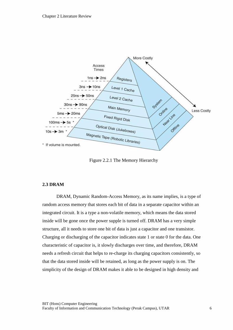
2.2 Memory Hierarchy
Basically, there is a tradeoff between access time, cost and capacity for
memories. Fast memories, that is, with short access time, like registers or cache are
low in capacity (a few MB) and high in cost. While cheap and large capacity
memories, which its capacity can go up to TBs (Terabytes), like the magnetic tape or
optical disk, its access time is extremely long.
Chapter 2 Literature Review
BIT (Hons) Computer Engineering
Faculty of Information and Communication Technology (Perak Campus), UTAR 6
Figure 2.2.1 The Memory Hierarchy
2.3 DRAM
DRAM, Dynamic Random-Access Memory, as its name implies, is a type of
random access memory that stores each bit of data in a separate capacitor within an
integrated circuit. It is a type a non-volatile memory, which means the data stored
inside will be gone once the power supple is turned off. DRAM has a very simple
structure, all it needs to store one bit of data is just a capacitor and one transistor.
Charging or discharging of the capacitor indicates state 1 or state 0 for the data. One
characteristic of capacitor is, it slowly discharges over time, and therefore, DRAM
needs a refresh circuit that helps to re-charge its charging capacitors consistently, so
that the data stored inside will be retained, as long as the power supply is on. The
simplicity of the design of DRAM makes it able to be designed in high density and

Chapter 2 Literature Review
BIT (Hons) Computer Engineering
Faculty of Information and Communication Technology (Perak Campus), UTAR 7
yet low cost, meaning it can stores more data within the same area, or stores the same
amount of data with smaller area, compared to other types of memory, such as
SDRAM. Just for information, SRAM (Static Random Access Memory) is another
type of non-volatile memory which uses 6 or 8 transistors to store 1 bit of data. Look
at the one capacitor plus one transistor design of DRAM and 6 transistors design of
SRAM, it is obvious that why the DRAM is said to be a cheaper and smaller type of
memory. However, when it comes to comparing the access time of these 2 types of
memory, it is also obvious that turning on or off the transistors is way faster than
charging or discharging a capacitor. Hence, DRAM is a type of memory which is
cheap and small, but access time is long.
DRAM
SRAM
Figure 2.3.1 Structures of DRAM and SRAM
2.4 SDRAM
Synchronous Dynamic Random Access Memory (SDRAM) is a type of
DRAM that is synchronised with the system bus. It waits for a transition of clock to
respond to the control signals and inputs, unlike the asynchronous ones which respond

Chapter 2 Literature Review
BIT (Hons) Computer Engineering
Faculty of Information and Communication Technology (Perak Campus), UTAR 8
instantly to the changes of control signals and inputs. This project uses a SDRAM that
is provided by MICRON Technology Inc. It is MT48LC4M32B2, with 16MB of
storage. It has a positive edge clock pin, means it will wait for a rising edge of the
clock signal before responding to the control signals or inputs.
Figure 2.4.1 Block diagram of MT48LC4M32B2
Figure 2.4.1 shows the block diagram of MT48LC4M32B2, it has 128Mb or 16MB of
storage. Pin ba[1:0] is use to select its 4 internal memory banks. It has a 12-bits wide
port for input of the address. 16MB of storage should need 24-bits to represent all the
locations, but how does this SDRAM make it with 12-bits address port? First, each
location inside its internal memory banks stores 32bits of data, which is 4 Bytes. This
reduces the required address bits from 24 to 22. As mentioned earlier, it has a 2-bits
port for internal bank selecting, that takes another 2-bits of address and now we left

Chapter 2 Literature Review
BIT (Hons) Computer Engineering
Faculty of Information and Communication Technology (Perak Campus), UTAR 9
with 20bits of address. Actually this SDRAM reads address separately, the addresses
need to be separated into 12-bits of Row address and 8-bits of Column address. The
row and column address are meant to be input into the SDRAM at different clock
cycles, this is why a 12-bits address port is enough for the use. This address port is
also used for configuring setting to the SDRAM.
Figure 2.4.2 A simplified view on how the SDRAM arrays are addressed
Pin dq[31:0] is the I/O port for the data, it is bidirectional, data that to be read from or
write into the SDRAM goes or comes via this port. dqm[3:0] is used to mask the
output or input of the data, since the data width is 32-bits, which is 4Bytes, each bit of
the dqm is corresponds to each byte of the data for masking. The granularity of a bus
is defined as the smallest transfer can be done by that bus. In this case, the granularity
of this SDRAM is 8-bits. The CS pin is used to select the SDRAM chip, it is active
low. Meanwhile active low command signals (we, cas and ras) are used to request
operations from the SDRAM.

Chapter 2 Literature Review
BIT (Hons) Computer Engineering
Faculty of Information and Communication Technology (Perak Campus), UTAR 10
Table 2.4.1 List of SDRAM commands and their respective function
As mentioned before, the address port can be used to configure the mode of
operations for the SDRAM. There is an operation mode called Burst mode. Burst is a
technique used to continuous read or write data from the memory depends on the
burst length. For example, if we programmed the SDRAM into burst mode with burst
length of 8, then 8 words (32-bits) of data will be read out continuously when it is in
READ operation, or 8 words of data will be written into 8 continuous locations
continuously when it is in WRITE operation. This mode is extremely useful, it
reduces a lot of access time for the cache, because the transfer of data for cache is by
block, each block of the cache has 8 words of data (32 Bytes).

Chapter 2 Literature Review
BIT (Hons) Computer Engineering
Faculty of Information and Communication Technology (Perak Campus), UTAR 11
Figure 2.4.3 Mode Register definition

Chapter 2 Literature Review
BIT (Hons) Computer Engineering
Faculty of Information and Communication Technology (Perak Campus), UTAR 12
Burst Length
Used to determine maximum number of column locations that can be accessed
for a given READ or WRITE operation.
Burst Type
Used to select either sequential or interleaved burst to be adopted by SDRAM.
The ordering of accesses within a burst is determined by burst length, burst
type, starting column address.
CAS Latency
Delay in clock cycles between registration of a READ command and the
availability of the first piece of output data. It can only be set to 2 or 3 clock
cycles.
Operating Mode
Used to select which operating mode should the SDRAM be. Currently there
is only normal operating mode is available for use.
Writing Burst Mode
When it is „0‟, the burst length is programmed via M0-M2 applies to both
READ and WRITE burst.
When it is „1‟, the programmed burst length applies to READ bursts, but write
accesses are single-location (non-burst) accesses.

Chapter 2 Literature Review
BIT (Hons) Computer Engineering
Faculty of Information and Communication Technology (Perak Campus), UTAR 13
2.5 SDRAM Controller
A SDRAM controller has been modelled based on industry standard
WISHBONE SoC interface by Oon Zhi Kang. SDRAM Controller is to do the
communication between the host and SDRAM. The SDRAM Controller receive the
operation command from the host, it will interpret it and translate into a control signal
which acts as an input to the SDRAM.
Figure 2.5.1 Block diagram of SDRAM Controller
Pin Name Size (bits) Description
ip_wb_clk 1 Clock signal to synchronize to the system.
ip_wb_rst 1 Synchronous reset to reinitialize the system.
ip_wb_cyc 1 Asserted (HIGH) to indicate valid bus cycle is in
progress.
ip_wb_stb 1 Asserted (HIGH) to indicate the SDRAM controller
is selected.
4

Chapter 2 Literature Review
BIT (Hons) Computer Engineering
Faculty of Information and Communication Technology (Perak Campus), UTAR 14
Table 2.5.1 I/O pin description of SDRAM Controller.
ip_wb_we 1 Asserted (LOW) to indicate that the current cycle is
READ. Deasserted (HIGH) to indicate current cycle
is WRITE.
op_wb_ack 1 Asserted (HIGH) to indicate that the current READ
or WRITE operation is successful.
ip_wb_sel [3:0] 4 Used to indicate where valid data is placed on the
input data line (ip_wb_dat) during WRITE cycle and
where it should present on the output data line
(op_wb_dat) during READ cycle.
ip_wb_addr [31:0] 32 Used to pass the memory address from the host.
ip_wb_dat [31:0] 32 Used to pass WRITE data from the host.
op_wb_dat [31:0] 32 Used to output READ data from the SDRAM.
ip_host_ld_mode 1 Asserted to load a new mode into the SDRAM.
op_sdr_cs_n
1 SDRAM chip select.
op_sdr_ras_n
1 SDRAM row address select.
op_sdr_cas_n 1 SDRAM column address select.
op_sdr_we_n
1 SDRAM write enable.
op_sdr_addr [11:0] 12 Address output to the SDRAM.
op_sdr_ba [1:0] 2 Bank Address output to SDRAM.
op_sdr_dqm [3:0] 4 Used to select which bits of the data line (io_sdr_dq)
to be masked.
io_sdr_dq [31:0] 32 Bidirectional data line to receive READ data or send
WRITE data.

Chapter 2 Literature Review
BIT (Hons) Computer Engineering
Faculty of Information and Communication Technology (Perak Campus), UTAR 15
Figure 2.5.2 The Microarchitecture of SDRAM Controller.

Chapter 2 Literature Review
BIT (Hons) Computer Engineering
Faculty of Information and Communication Technology (Perak Campus), UTAR 16
The previous figure shows the microarchitecture of the SDRAM Controller. The
block sdc_obrt_top_obrt_unit is used to track the row status of all of the banks. Block
sdc_mc is responsible to store the status of the SDRAM configuration and also the
power up status to indicate if the SDRAM controller is executing the initialization
protocol or not. The address multiplexer, sdc_addr_mux partitions the WISHBONE
address input line into row address, bank address and column address. Then, it
multiplexes the configuration mode, row address and column address. It also decodes
the WISHBONE Select input pin and converts it to equivalent masking output.
Besides, block sdc_dp_buf is used to controls the flow of the data between
SDRAM and Host while block sdc_sdram_ifis the SDRAM Interface Block that
synchronizes all the signals to the negative edge before sending them out the SDRAM.
Other than that, SDRAM Controller also responsible to instruct the SDRAM
to initiate a precharge in order to maintain the information stored inside each cell.
Otherwise, the information stored inside each cell will be lost due to the characteristic
of capacitor which is the voltage will slowly leak off. The finite state machine below
shows how the SDRAM Controller handles the timing and the state changes that
forms the protocols of the SDRAM. It helps in decide which protocol to be executed
and what commands to be sent to the SDRAM by using the sdc_fsm block. Note that
branches without condition has the lowest priority.

Chapter 2 Literature Review
BIT (Hons) Computer Engineering
Faculty of Information and Communication Technology (Perak Campus), UTAR 17
Figure 2.5.3 Protocol Controller Block FSM

Chapter 2 Literature Review
BIT (Hons) Computer Engineering
Faculty of Information and Communication Technology (Perak Campus), UTAR 18
Table 2.5.2 State definition of Protocol Controller
Table 2.5.3 Branch conditions of Protocol Controller

Chapter 2 Literature Review
BIT (Hons) Computer Engineering
Faculty of Information and Communication Technology (Perak Campus), UTAR 19
State Name Correspondence Output Behaviors
INIT op_fsm_cmd<= `CMD_NOP;
r_brst_cnt<= 0;
r_pu_cnt<= 2;
r_ri_cnt<= `REF_INTERVAL;
r_tmr_val<= `WAIT_150us;
op_wb_ack<= 0;
INIT_W op_fsm_cmd<= `CMD_NOP;
PRECH op_fsm_cmd<= `CMD_PRECH;
op_fsm_bank_clr<= !(w_ref_req | ip_fsm_pu_stat);
op_fsm_bank_clr_all<= (w_ref_req | ip_fsm_pu_stat |
ip_host_ld_mode);
op_fsm_a10_cmd <= (w_ref_req | ip_fsm_pu_stat |
ip_host_ld_mode);
r_tmr_val<= `TRP_DEF – 13‟d1;
PRECH_W op_fsm_ld_mode_req<= ip_host_ld_mode;
op_fsm_cmd<= `CMD_NOP;
AREF op_fsm_cmd<= `CMD_AREF;
r_pu_cnt<= ip_fsm_pu_stat? r_pu_cnt – 1: r_pu_cnt;
r_ri_cnt<= `REF_INTERVAL;
r_tmr_val<= tRFC constant – 1;
AREF_W op_fsm_cmd<= `CMD_NOP;
r_ri_cnt<= `REF_INTERVAL;
LMR op_fsm_cmd<= `CMD_LMR;
op_fsm_lmr_sel<= 1;
op_fsm_pu_done<= ip_fsm_pu_stat? 1: 0;
r_tmr_val<= {2‟b00, `TMR_DEF} – 13‟d1;
op_wb_ack<= ip_wb_cyc&ip_wb_stb&ip_host_ld_mode;
IDLE_0 op_fsm_cmd<= `CMD_NOP;

Chapter 2 Literature Review
BIT (Hons) Computer Engineering
Faculty of Information and Communication Technology (Perak Campus), UTAR 20
IDLE op_fsm_cmd<= `CMD_NOP;
ACT op_fsm_cmd<= `CMD_ACT;
op_fsm_bank_act<= 1
op_fsm_row_sel<= 1;
r_tmr_val<= {1‟b0,`TRCD_DEF} – 13‟d1;
WRITE op_fsm_cmd<= `CMD_WR;
r_brst_cnt<= r_brst_val – 1;
r_tmr_val<= {2‟b00,`TWR_DEF} – 13‟d1;
op_fsm_woe<= 1;
op_wb_ack<= ip_wb_cyc&ip_wb_stb;
WRITE_LOOP op_fsm_cmd<= `CMD_NOP;
r_brst_cnt<= r_brst_cnt – 1;
r_tmr_val<= {2‟b00,`TWR_DEF} – 13‟d1;
op_fsm_woe<= 1;
op_wb_ack<= ip_wb_cyc&ip_wb_stb;
READ op_fsm_cmd<= `CMD_RD;
r_brst_cnt<= r_brst_val;
r_tmr_val<= {1‟b0,ip_fsm_cfg_mode[6:4]} – 13‟d1;
READ_W op_fsm_cmd<= `CMD_NOP;
READ_LOOP op_wb_ack<= ip_wb_cyc&ip_wb_stb&r_roe;
op_fsm_cmd<= `CMD_NOP;
r_brst_cnt<= r_brst_cnt – 1;
r_roe<= 1;
BT op_fsm_cmd<= `CMD_BT;
r_brst_cnt<= 0;
Table 2.5.4 Outputs of the states of Protocol Controller

Chapter 2 Literature Review
BIT (Hons) Computer Engineering
Faculty of Information and Communication Technology (Perak Campus), UTAR 21
The FSM of the Protocol Controller contains all the main states of the SDRAM
controller, operations that need to be done by SDRAM are specified clearly. The
SDRAM controller can issue the refresh command to SDRAM itself when necessary,
without having the command from host. The FSM may seem large and complex, but
we can have a better understanding if we break the whole FSM into several processes.
Chapter 2 Literature Review
BIT (Hons) Computer Engineering
Faculty of Information and Communication Technology (Perak Campus), UTAR 22
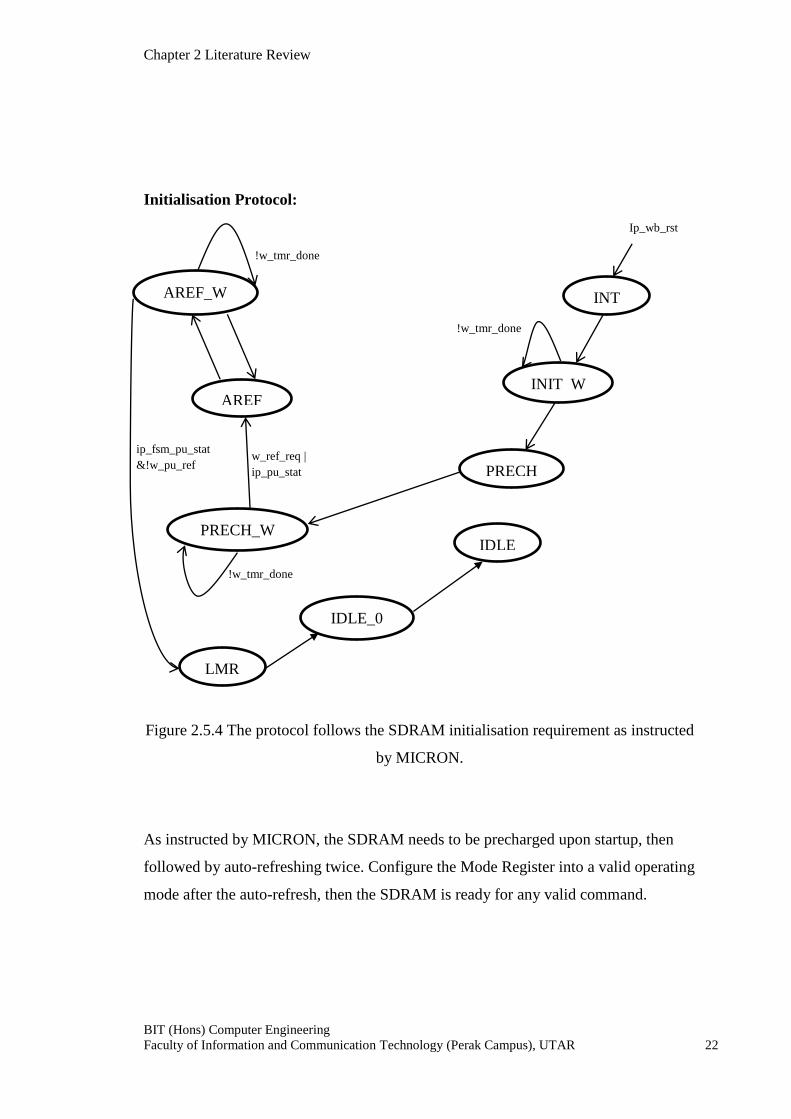
Initialisation Protocol:
Figure 2.5.4 The protocol follows the SDRAM initialisation requirement as instructed
by MICRON.
As instructed by MICRON, the SDRAM needs to be precharged upon startup, then
followed by auto-refreshing twice. Configure the Mode Register into a valid operating
mode after the auto-refresh, then the SDRAM is ready for any valid command.
INIT_W
PRECH
AREF
LMR
AREF_W INT
PRECH_W IDLE
ip_fsm_pu_stat
&!w_pu_ref w_ref_req |
ip_pu_stat
!w_tmr_done
!w_tmr_done
Ip_wb_rst
IDLE_0
!w_tmr_done

Chapter 2 Literature Review
BIT (Hons) Computer Engineering
Faculty of Information and Communication Technology (Perak Campus), UTAR 23
Keep Bank and Row Open Access Protocol:
Figure 2.5.5 Keep Bank and Row Open Access Protocol to achieve fast access cycle
for same row access
Before we want to access a particular location for read or write, we have to open the
particular row of the particular bank of the location. Opening a row is simply
activating it, but if there is already a different row opened in the same bank, that row
will need to be closed first before opening the desired row. Closing of a row is by
precharging it. Different bank can have different row opened at the same time, this
will not violates the read or write operations in the individual banks.
PRECH
PRECH_W
IDLE
!w_tmr_done
(ip_host_ld_mode&ip_ fsm_any_bank_open) |
(w_ref_req&ip_ fsm_any_bank_open) |
((w_rd_req | w_wr_req) & !ip_ fsm_row_same)
ACT
(w_rd_req | w_wr_req)
& !ip_ fsm_bank_open

Chapter 2 Literature Review
BIT (Hons) Computer Engineering
Faculty of Information and Communication Technology (Perak Campus), UTAR 24
Load Mode Protocol (Post Initialisation):
Figure 2.5.6 Load Mode Protocol
Although a valid operating mode is programmed upon the initialisation of the
SDRAM, it can be re-programmed to another operating mode as desired. According
to the MICRON, before you can load a new mode into the mode register, all banks
must be in idle state, that is, no row is opened. If the SDRAM doesn‟t have any row
opened already, then the new mode can be programmed into the mode register right
away. But if there are any opened row in any bank, then the SDRAM will need to be
precharged before loading a new mode into mode register.
PRECH
LMR
PRECH_W
IDLE
!w_tmr_done ip_host_ld_mode
(ip_host_ld_mode&ip_ fsm_any_bank_open) |
(w_ref_req&ip_ fsm_any_bank_open) |
((w_rd_req | w_wr_req) & !ip_ fsm_row_same)
IDLE_0
ip_host_ld_mode& !ip_fsm_any_bank_ope
n

Chapter 2 Literature Review
BIT (Hons) Computer Engineering
Faculty of Information and Communication Technology (Perak Campus), UTAR 25
Auto Refresh Protocol:
Figure 2.5.7 Auto Refresh Protocol
As mentioned in the earlier section, DRAMs need to be consistently refresh due to its
capacitors inside will slowly discharge and the stored data will fades away with it. It
would be troublesome and inefficient if the host has to issue the refresh command
every time the SDRAM needs one. But this protocol can do the auto-refresh itself
without having the host to issue. According to the MICRON, all banks must be
precharged before an auto-refresh, if all the banks are idle already, then the auto-
refresh can be performed right away. But if any of the banks are open, then will have
to precharged them before the auto-refresh.
PRECH
AREF
AREF_
PRECH_
IDLE
!w_tmr_done
w_ref_req |
ip_pu_stat
!w_tmr_done
(ip_host_ld_mode&ip_ fsm_any_bank_open)
| (w_ref_req&ip_ fsm_any_bank_open) |
((w_rd_req | w_wr_req) & !ip_
fsm_row_same) w_ref_req&!ip_fsm_
anybank_open

Chapter 2 Literature Review
BIT (Hons) Computer Engineering
Faculty of Information and Communication Technology (Perak Campus), UTAR 26
Read and Write Protocol:
Figure 2.5.8 Read Protocol
IDLE READ
READ_W
BT
IDLE_0 READ_LOOP
!w_tmr_done
!w_rd_req
!w_rd_req&
w_brst_active
w_rd_req&
ip_ fsm_row_same
&ip_ fsm_bank_open
PREC
H
PRECH_W
ACT
!w_tmr_done
(ip_host_ld_mode&ip_ fsm_any_bank_open) |
(w_ref_req&ip_ fsm_any_bank_open) |
((w_rd_req | w_wr_req) & !ip_ fsm_row_same)
!w_tmr_done

Chapter 2 Literature Review
BIT (Hons) Computer Engineering
Faculty of Information and Communication Technology (Perak Campus), UTAR 27
Figure 2.5.9 Write Protocol
IDLE
BT
WRITE
WRITE_LOOP
IDLE_0
!w_rd_req&w_b
rst_active
!w_brst_active
w_wr_req&
ip_ fsm_row_same
&ip_ fsm_bank_open
PREC
H
PRECH_W
ACT
(w_rd_req | w_wr_req)
& !ip_ fsm_bank_open
!w_tmr_done
(ip_host_ld_mode&ip_ fsm_any_bank_open) |
(w_ref_req&ip_ fsm_any_bank_open) |
((w_rd_req | w_wr_req) & !ip_ fsm_row_same)
!w_tmr_done

Chapter 2 Literature Review
BIT (Hons) Computer Engineering
Faculty of Information and Communication Technology (Perak Campus), UTAR 28
Actually the read protocol and write protocol are pretty much the same. As mentioned
in the Keep Bank and Row Open Access Protocol, we need to activate the particular
row before we want to access one of its columns for read or write. This is why we are
seeing something similar with the Keep Bank and Row Open Access Protocol on the
Read Protocol and Write Protocol.
Before accessing a particular location for reading or writing, its row needs to
be activated. If there is already another opened row in the bank, then the opened row
will need to be closed, that is, precharged, before activating the desired row. If the
bank is already idle, then we can straight away activate the desired row. If the desired
row has already opened, then the activation of row can be skipped.
Then we can access the desired column for reading or writing. If the SDRAM
was in Single Location Access Mode, only the data in that location will be read or
written. If the SDRAM was in Burst Mode, then the data in that location and the data
in consecutive locations will be read or written, depends on the programmed burst
length.

Chapter 2 Literature Review
BIT (Hons) Computer Engineering
Faculty of Information and Communication Technology (Perak Campus), UTAR 29
2.6 Cache
A 2-way set associative cache of 2MB has been modelled by Khoo Chong
Siang. Caches are used as small but fast buffers for the main memory so that the CPU
can have a faster access time to the data inside main memory.
Figure 2.6.1 Cache Unit designed by Khoo Chong Siang
This cache can be used as both Instruction Cache and Data Cache. It is to be
connected to the CPU. It is also wishbone compatible. When it comes to design a
cache, we have to consider the scenarios to have a better understanding on cache
behaviours.
Chapter 2 Literature Review
BIT (Hons) Computer Engineering
Faculty of Information and Communication Technology (Perak Campus), UTAR 30
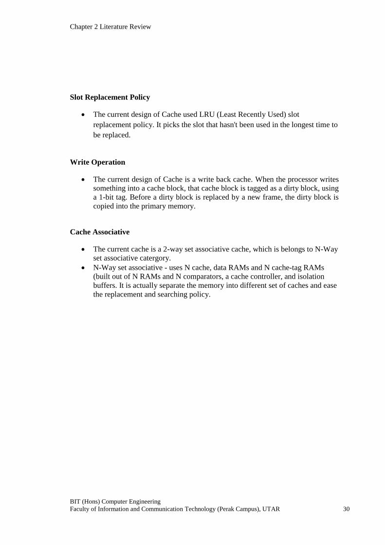
Slot Replacement Policy
The current design of Cache used LRU (Least Recently Used) slot
replacement policy. It picks the slot that hasn't been used in the longest time to
be replaced.
Write Operation
The current design of Cache is a write back cache. When the processor writes
something into a cache block, that cache block is tagged as a dirty block, using
a 1-bit tag. Before a dirty block is replaced by a new frame, the dirty block is
copied into the primary memory.
Cache Associative
The current cache is a 2-way set associative cache, which is belongs to N-Way
set associative catergory.
N-Way set associative - uses N cache, data RAMs and N cache-tag RAMs
(built out of N RAMs and N comparators, a cache controller, and isolation
buffers. It is actually separate the memory into different set of caches and ease
the replacement and searching policy.

Chapter 2 Literature Review
BIT (Hons) Computer Engineering
Faculty of Information and Communication Technology (Perak Campus), UTAR 31
Scenarios to Represent Cache Behaviours
Basically there are just 4 scenarios might be happened on cache, we need to decide
what to do when these scenarios happen.
1. Read Miss
Receive physical address and instructions of read from the main
controller of the CPU.
Check validity and tag for the index of the physical address points to.
A miss signal is produced due to either it is invalid or the tag is
different.
Cache controller asserts strobe, cycle, and read signals to SDRAM
controller to fetch new black of data.
Meanwhile, the pipelines of the CPU are stalled.
Check LRU to determine which slot is least recently used, store the
newly fetched block of data in it.
Set valid bit for the index pointed.
Update LRU.
Deassert the miss, strobe, cycle and read signal, the pipelines are
un-stalled.
2. Read Hit
Receive physical address and instruction of read from the main
controller of CPU.
Check validity and tag for index of the physical address points to.
Miss signal is active low.
Load the selected instruction or data by determining the byte offset to
host.
Update LRU.

Chapter 2 Literature Review
BIT (Hons) Computer Engineering
Faculty of Information and Communication Technology (Perak Campus), UTAR 32
3. Write Miss (For D-Cache only)
Receive physical address, data, and instruction of write from the main
controller of CPU.
Check validity and tag for the index of the physical address points to.
A miss signal is produced due to either it is invalid or the tag is
different.
Stall the pieplines.
Check LRU to determine which is least recently used.
Cache controller asserts strobe, cycle, and read to SDRAM controller
to access the data in SDRAM.
If the block of data was dirty, send the block of 8 words back to
SDRAM.
Fetch new block of data from SDRAM.
After the new block is updated from SDRAM, strobe, cycle, read and
miss signals are deasserted.
Perform the write.
Update LRU.
4. Write Hit (For D-Cache only)
Receive physical address, data, and instruction of write from main
controller of CPU.
Check validity of tag for index of the physical address points to. Miss
signal is active low.
Update the selected instruction or data.
Update LRU.

Chapter 2 Literature Review
BIT (Hons) Computer Engineering
Faculty of Information and Communication Technology (Perak Campus), UTAR 33
Cache Design Protocol
The read and write operation are separated into two different ASM. After that it will
be used to design the finite state machine of the cache controller.
Figure 2.6.2 Read Protocol of Cache

Chapter 2 Literature Review
BIT (Hons) Computer Engineering
Faculty of Information and Communication Technology (Perak Campus), UTAR 34
Figure 2.6.3 Write Protocol of Cache

Chapter 2 Literature Review
BIT (Hons) Computer Engineering
Faculty of Information and Communication Technology (Perak Campus), UTAR 35
Cache Operations
Four scenarios might be happened on cache, which are read miss, read hit, write miss
and write hit. In order to design the datapath of the cache, four diagrams are drawn
and they all show the operations that are performed during the different scenarios.
Figure 2.6.4 Read Hit

Chapter 2 Literature Review
BIT (Hons) Computer Engineering
Faculty of Information and Communication Technology (Perak Campus), UTAR 36
Figure 2.6.5 Read Miss

Chapter 2 Literature Review
BIT (Hons) Computer Engineering
Faculty of Information and Communication Technology (Perak Campus), UTAR 37
Figure 2.6.6 Write Miss

Chapter 2 Literature Review
BIT (Hons) Computer Engineering
Faculty of Information and Communication Technology (Perak Campus), UTAR 38
Figure 2.6.7 Write Hit

Chapter 2 Literature Review
BIT (Hons) Computer Engineering
Faculty of Information and Communication Technology (Perak Campus), UTAR 39
2.7 Translation Lookaside Buffer (TLB)
A Translation Lookaside Buffer (TLB) has been modelled by Kim Yuh
Chang. Before we talk about what is a TLB, let‟s talk about physical address and
virtual address. Virtual memory and virtual address is the reason that the systems are
able to run multiple programs at a time. Look that the following virtual memory map
that based on 32-bits MIPS:
Figure 2.7.1 Virtual Memory Map based on 32-bits MIPS
As a programmer, when we write programs, we do not have to consider
other programs that might be running on the same system with our program. The
program we write will just have to follow the above memory map, for example, code
segment at 0x0040_0000, data segment at 0x1000_000 and etc. If these are all
physical addresses, how is it possible for a system to run a few programs at the same
time? We can‟t have a few addresses of 0x0040_0000 and a few addresses of
0x1000_000. Furthermore, not every 32-bits system is acquired with 4GB of main

Chapter 2 Literature Review
BIT (Hons) Computer Engineering
Faculty of Information and Communication Technology (Perak Campus), UTAR 40
memory, take this project as an example, the SDRAM we are using is just 16MB, and
address of 0x1000_0000 is definitely exceeded the boundary of 16MB. So how can a
program runs on different system with different memory specifications? Well the
answer is obvious, virtual memory and virtual address.
These virtual memory and virtual address is a barrier to hide the memory
specifications against the users or programmers. Everybody will see all the 32-bits
systems are pretty much the same. When a program runs, its code and data are loaded
into the main memory, the locations in the main memory where these codes and data
are actually stored are the physical addresses. There will be a segment in the main
memory which stores the page tables. Page tables store virtual page number and their
corresponding physical page number, as well as other essential information such as
the process ID. These page tables are managed by the operating system (OS).
Figure 2.7.2 An example of address translation

Chapter 2 Literature Review
BIT (Hons) Computer Engineering
Faculty of Information and Communication Technology (Perak Campus), UTAR 41
Figure 2.7.3 An overall picture of how virtual memory works.
Now is the time Translation Lookaside Buffer (TLB) comes in. When we
want to translate a virtual address to physical address, we will have to refer to the
page numbers in page tables inside the main memory. But directly accessing the main
memory is so low, we need a small and fast buffer to store a fraction of the page
tables. Sounds familiar? Yes, actually TLB is just a cache for the page tables in main
memory. Unlike the cache that modelled by Khoo, which is 2-way set associative, the
TLB that Kim modelled is fully associative and with 64 entries. Fully associative
means the data can be stored in any location in the cache. In our case, we just write
the page table entries into random one of the location in TLB

Chapter 2 Literature Review
BIT (Hons) Computer Engineering
Faculty of Information and Communication Technology (Perak Campus), UTAR 42
Figure 2.7.4 An example of how an 8-block cache configures as direct mapped, two-
way set assoiciative, four-way set associative and fully associative cache.
Although we say that the TLB is a cache, but it is a special cache. The things that a
TLB entry stores are very different from what ordinary caches store.
Virtual Page Number
(20 bits)
Control Bits Physical Page Number
(20 bits)
Figure 2.7.5 Contents of a TLB entry

Chapter 2 Literature Review
BIT (Hons) Computer Engineering
Faculty of Information and Communication Technology (Perak Campus), UTAR 43
Figure 2.7.6 Usage of TLB in address translation by using 48 entries and fully
associative TLB.
*Note that,
VPN is included inside as part of the TLB entry contents which is different
from the page table entry.
VPN doesn’t segment into 1st page table index and 2
nd page table index. This
is because when we are using TLB, it is containing the information in 2nd
level
page table only.
Control bits can be any bits which used to represent the status of each entry
based on the design needs.
o Example of control bits will be
Valid Bit, which used to represent the location of the page
whether in physical memory or disk.

Chapter 2 Literature Review
BIT (Hons) Computer Engineering
Faculty of Information and Communication Technology (Perak Campus), UTAR 44
Virtually addressed and Physically Address Cache
The placement of TLB can be either in series with caches or parallel with
caches. Both of the design have their pros and con. When we set the TLB in front of
the cache, this will mean that all of the address need to be translates into physical
address before access into cache. By using this design, the processing speed will be
reduced because we need to access to TLB first then only can access cache which
means we need to times two the access time to a cache. Although the processing
speed will be reduce, this method will be much simpler compare with a virtually
addressed cache.
Figure 2.7.7 The design of physically addressed cache.
There is another design of the placement of TLB which is the TLB works
parallel with the caches. This will reduce the processing time because the address
translation and the data searching can be done in parallel. Although this method can
enhance the efficiency of the processor, the design is more complex compare with
physically address cache because the lower 12 bits, page offset is used to search the
data in cache and the tag inside cache entries is output from the cache to compare with
the PFN output from TLB to determine whether it is a cache hit or miss. Problem
arises when we have two cache entries with the same page offset, which will cause an
aliasing effect. Therefore, additional logic needs to be added to eliminate this problem.
Figure 2.7.8 The design of virtually addressed cache.

Chapter 2 Literature Review
BIT (Hons) Computer Engineering
Faculty of Information and Communication Technology (Perak Campus), UTAR 45
Current design of TLB
Figure 2.7.9 Current design of TLB by Kim Yuh Chang

Chapter 2 Literature Review
BIT (Hons) Computer Engineering
Faculty of Information and Communication Technology (Perak Campus), UTAR 46
Figure 2.7.10 Current design of MMU by Kim Yuh Chang
These are the current design of the TLB, note that the MMU is a controller for the
TLB. Current design of TLB uses 2-level page table, which can greatly reduce the
size of page table compared to a 1-level page table, but as a trade-off, we will need to
access the main memory once more when we want to fetch new page table entry into
the TLB.

Chapter 2 Literature Review
BIT (Hons) Computer Engineering
Faculty of Information and Communication Technology (Perak Campus), UTAR 47
Figure 2.7.11 Segmentation of virtual address of current design
How does a 2-level page table works? Here is the way:
1. Given a virtual address
2. Use 1st level page table index to allocate the address of 2
nd level page table.
3. Use 2nd
level page table index to find out the PPN which is used to
concatenate with the page offset to form physical address.
4. Use physical address to get data from physical memory.

Chapter 2 Literature Review
BIT (Hons) Computer Engineering
Faculty of Information and Communication Technology (Perak Campus), UTAR 48
Figure 2.7.12 The usage of 2-level page table in address translation

Chapter 3 Methodology and Development Tools
BIT (Hons) Computer Engineering
Faculty of Information and Communication Technology (Perak Campus), UTAR 49
Chapter 3: Methodology and Development Tools
3.1 Methodology
Design methodology refers to the methods to develop a system. It is a guide
on how to do design work successfully. A good design methodology needs to ensure
the following:
Correct Functionality
Satisfaction of performance and power goals
Catching bugs early
Good documentation
The ideal design flow for this project would be the top-down methodology as shown
in the following figure.

Chapter 3 Methodology and Development Tools
BIT (Hons) Computer Engineering
Faculty of Information and Communication Technology (Perak Campus), UTAR 50
Figure 3.1.1 General Design Flow without Synthesis and Physical Design
3.1.1 System Level Design
System Level Design is level where chip specifications are being develop. System
level design includes the following two types:
Written specification: Is an English-written specification of function,
performance, cost and time constrain of a design. This Specification should
also include function specification, verification specification, packaging
specification and development plan.

Chapter 3 Methodology and Development Tools
BIT (Hons) Computer Engineering
Faculty of Information and Communication Technology (Perak Campus), UTAR 51
Executable specification: Using high-level programming language to
describe the features and functionalities. High-level programming language
referring to VERILOG, VHDL and etc. which is executable.
3.1.2 Architecture Level Design
Architecture Level Design can categorize into 2 phases:
Architecture specification: Architecture specification describe internal of a
chip and may contain design partitioning of the chip into units, basic
connection or interface between units, I/O timing and delay requirements of
the units and critical algorithms used.
Architecture Level Modelling and Verification: An algorithm is developed
to model the unit base on architecture specification. In this phase, each unit is
verified for functional correctness.
3.1.3 Micro-architecture Level Design
In this level, RTL (Register Transfer Level) is developed. A micro-architecture
specification of each unit, which used to describe the internal design of architecture
block module. Micro-architecture specification may include information of:
An overview of the functional description
I/O pin description
I/O timing requirements
Function table
Finite-state machine (FSM) and Algorithmic-state machine.
Test Plan

Chapter 3 Methodology and Development Tools
BIT (Hons) Computer Engineering
Faculty of Information and Communication Technology (Perak Campus), UTAR 52
After developed Micro-architecture Specification, RTL modelling with
programming language can be start. Model can be simulate and verified with software.
Verification includes development of test plan, timing verification and functionality
verification. Hence designer can verify and modify the design to meet the chip
specification.
3.2 Design Tools
3.2.1 Verilog HDL Simulator
Since this project use Verilog, this is a Hardware Description Language
(HDL). Simulations tools that support Verilog HDL is required, tools that provide
simulation environment to verify the functional and timing models of the design, and
the HDL source code. There are a lot HDL simulator created by different company,
which has their own advantages and disadvantages. In order to choose most
appropriate design tools for this project, some researches had been done and the
choices has been narrow into three choices, which are the best HDL simulation tools
available on the market, they are also known as the „Big 3‟ simulators, three major
signoff-grade simulators which qualified for application-specific integrated circuit
(ASIC) (validation) sign-off at nearly all semiconductor fabrications. They are:
1. Incisive Enterprise Simulator by Cadence Design Systems
2. ModelSim by Mentor Graphic
3. Verilog Compiled code Simulator (VCS) by Synopsys
However, to choose the most appropriate design tools for this project, some factors
such as price, availability, affordability, language supported, user friendly and
performance need to put in considerations. Since most of the simulators support
system-level & RTL design, some minor comparisons between the „big 3‟ HDL
simulator are shown in the table 4.1 below:

Chapter 3 Methodology and Development Tools
BIT (Hons) Computer Engineering
Faculty of Information and Communication Technology (Perak Campus), UTAR 53
Simulator Incisive Enterprise
Simulator ModelSim VCS
Company
Language
Supported
VHDL-2002
V2001
SV2005
VHDL-2002
V2001
SV2005
VHDL-2002
V2001
SV2005
Platform
supported
-Sun-solaris
-Linux
-Windows
XP/Vista/7
-Linux
-Linux
Availability
for free?
(SE edition only)
Table 3.1 Comparison between „Big 3‟ Simulators
Based on the above comparison, it is clear to state that ModelSim from Mentor
Graphic is the best choice as a design tools for this project as they offer a free license
for Student Edition, with some limitation, but it is sufficient for this project. It support
Microsoft Windows platform as well. While the other two simulators offer great
features as well, but the price are too expensive ($25,000 - $100,000) and not
affordable.
3.2.2 Mentor Graphics ModelSim SE 10.0a
ModelSim from Mentor Graphic is the industry-leading simulation and
debugging environment for HDL (Hardware Description Language) based design
which its license can be obtained for free. Both Verilog and VHDL are supported.
This software provides syntax error checking and waveform simulation. The timing

Chapter 3 Methodology and Development Tools
BIT (Hons) Computer Engineering
Faculty of Information and Communication Technology (Perak Campus), UTAR 54
diagrams and the waveforms of the inputs and outputs can be verified by writing a
program called a testbench in the simulation mode of the ModelSim. This software
ensures that the function of modules is working correctly. Student version instead of
full version of the ModelSim is sufficient enough for this project.
3.2.3 MIPS Simulator – PCSPIM
PCSPIM is a MIPS simulator. This program used for program writing and
simulation as similar to running a MIPS micro-processor. PCSPIM is translating the
MIPS assembly code into hex code. The hex code will port into Modelsim SE for
simulation and verification of RTL model. The limitation of using PCSPIM is
Branch delay – inside the setting, the branch delay should be disabled else the
program will include a delay slot which is not supported by
RISC32.
Branch address – the branch address in PCSPIM is incremented offset by 1 for
beginner‟s understanding. Thus, the program generated is
required to decrement the offset by 1.
3.2.4 RISC32 Assembly Language
The RISC32 instruction set is portion of MIPS32 instruction set. It is specified in the
written specification. This instruction set is used to verify the system in bus functional
model to ensure the correctness of the system. This instruction set is particular to the
RISC32 that enhanced. Any newly implemented instruction will require remodelling
of RISC32.

Chapter 4 Architecture of the RISC32
BIT (Hons) Computer Engineering
Faculty of Information and Communication Technology (Perak Campus), UTAR 55
Chapter 4: Architecture of the RISC32
Figure 4.0.1 Full RISC32‟s Architecture and Micro-architecture Partitioning.

Chapter 4 Architecture of the RISC32
BIT (Hons) Computer Engineering
Faculty of Information and Communication Technology (Perak Campus), UTAR 56
4.1 Design Hierarchy
Chip Partitioning at
Architecture Level
Unit Partitioning at Micro-
architecture Level
Block and Functional Block
Partitioning at RTL Level
(Micro-Architecture Level)
c_risc32_full u_data_path b_reg_file
b_alb_32
b_mult_32
b_branch_pred
u_ctrl_path b_alb_ctrl
b_iag_ctrl
b_main_ctrl
b_fwrd
b_itl_ctrl
u_mem_sys u_cache (for instruction)
u_cache (for data)
u_tlb (for instruction)
u_tlb (for data)
u_cp0 b_cp0_dc
b_cp0_regfile
Structural description Structural
description/Behavioral
description
Behavioral description
Table 4.1.1 Formation of a design hierarchy for Full RISC32 microprocessor through
top down design methodology
*Note that this design is provided as a mindset for future improvement.

Chapter 5 Memory System Design
BIT (Hons) Computer Engineering
Faculty of Information and Communication Technology (Perak Campus), UTAR 57
Chapter 5: Memory System Design
5.1 Memory System Specifications
RISC32 with Integrated Main Memory
SDRAM 16MB
Instruction TLB 64 Entries
Data TLB 64 Entries
Instruction Cache 2-way set associative, 2MB
Data Cache 2-way set associative, 2MB
Data Bus Width 32-bits
Instruction Width 32-bits
Table 5.1.1 Specifications of the Memory System
5.2 Naming Convention
Module – [lvl]_[mod. name]
Instantiation – [lvl]_[abbr. mod. name]
Pin – [lvl]_[abbr. mod. name]_[Type]_[pin name]
– [lvl]_[abbr. mod. name]_[Type]_[stage]_[pin name]

Chapter 5 Memory System Design
BIT (Hons) Computer Engineering
Faculty of Information and Communication Technology (Perak Campus), UTAR 58
Abbreviation:
Description Case Available Remark
lvl level lower c : Chip
u : Unit
b : Block
mod. name Module
Name
lower all any
abbr. mod.
name
Abbreviated
module
name
lower all any maximum 3 characters
Type Pin type lower o : output
i : input
r : register
w : wire
f- :function
stage Stage name lower all if, id, ex,
mem, wb
pin name Pin name lower all any Several word separate by
“_”
Table 5.2.1 Naming convention

Chapter 5 Memory System Design
BIT (Hons) Computer Engineering
Faculty of Information and Communication Technology (Perak Campus), UTAR 59
5.3 Memory Map
Segment Address Purpose
kseg2 – 1GB 0xFFFF FFFF
0xC000 0000
Kernel module,
Page Table allocated here
kseg1 – 512MB 0xBFFF FFFF
0xA000 0000
Boot Rom
I/O Register (if below 512MB)
kseg0 – 512MB 0x9FFF FFFF
0x8000 0000
Direct view of memory to 512MB
kernel code and data.
Exception and Page Table Base
Register allocated here.
kuseg – 2GB 0x7FFF FFFF
0x1000 8000
Stack Segment starts from the ending
address and expand down.
Heap Segment starts from the starting
address and expand top.
0x1000 7FFF
0x1000 0000
Data segment and Dynamic library
code.
0x09FFF FFFF
0x0040 0000
Code Segment, where the main
program stored.
0x003F FFFF
0x0000 0000
Reserved
Table 5.3.1 Virtual memory map of 32-bits MIPS

Chapter 5 Memory System Design
BIT (Hons) Computer Engineering
Faculty of Information and Communication Technology (Perak Campus), UTAR 60
Stack Segment o Use for storing automatic variables, which are variables that allocated
and de-allocated automatically when program flow.
Heap Segment o Use for dynamic memory allocation such as malloc(), realloc() and
free().
Data Segment
o Use for storing global or static variables that initialize by programmer.
Code Segment
o Use for storing codes of main program or main program instructions.

Chapter 5 Memory System Design
BIT (Hons) Computer Engineering
Faculty of Information and Communication Technology (Perak Campus), UTAR 61
5.4 Memory System Interface
Figure 5.4.0.1 Block Diagram of u_mem_sys

Chapter 5 Memory System Design
BIT (Hons) Computer Engineering
Faculty of Information and Communication Technology (Perak Campus), UTAR 62
5.4.1 I/O Description
5.4.1.1 Input Pins
Pin Name:
u_mem_sys_i_sdrcntr_ack
Source Destination:
SDRAM CNTR Memory
System
Registered:
No
Pin Function:
Acknowledge signal (active HIGH) to indicate read or write to SDRAM is done.
Pin Name:
u_mem_sys_i_sdrcntr_data[31:0]
Source Destination:
SDRAM CNTR Memory
System
Registered:
No
Pin Function:
32-bits data that read from SDRAM.
Pin Name:
u_mem_sys_i_cp0_entrylo[31:0]
Source Destination:
CP0 Memory System
Registered:
No
Pin Function:
32-bits data that comes from the EntryLo register of CP0.
Pin Name:
u_mem_sys_i_cp0_entryhi[31:0]
Source Destination:
CP0 Memory System
Registered:
No
Pin Function:
32-bits data that comes from the EntryHi register of CP0.
Pin Name:
u_mem_sys_i_cp0_random[31:0]
Source Destination:
CP0 Memory System
Registered:
No
Pin Function:
32-bits data that come from the random register of CP0.

Chapter 5 Memory System Design
BIT (Hons) Computer Engineering
Faculty of Information and Communication Technology (Perak Campus), UTAR 63
Pin Name:
u_mem_sys_i_cp0_status[31:0]
Source Destination:
CP0 Memory System
Registered:
No
Pin Function:
32-bits data that comes from status register of CP0.
Pin Name:
u_mem_sys_i_cp0_baddr[31:0]
Source Destination:
CP0 Memory System
Registered:
No
Pin Function:
32-bits data that comes from baddr register of CP0.
Pin Name:
u_mem_sys_i_cpu_pc[31:0]
Source Destination:
CPU Memory System
Registered:
No
Pin Function:
Program Counter (PC) that comes from CPU to retrieve instructions inside I-Cache.
Pin Name:
u_mem_sys_i_cpu_data[31:0]
Source Destination:
CPU Memory System
Registered:
No
Pin Function:
32-bits data that comes from MEM stage of the pipelines. It will be written into the
D-Cache if u_mem_sys_i_cpu_wr is asserted.
Pin Name:
u_mem_sys_i_cpu_addr[31:0]
Source Destination:
CPU Memory System
Registered:
No
Pin Function:
32-bits address that comes from MEM stage of the pipelines. It indicates which
location should the data to be read from or write to.
Pin Name:
u_mem_sys_i_cpu_re
Source Destination:
CPU Memory System
Registered:
No
Pin Function:
Control signal that comes from MEM stage of the pipelines. When it is asserted
(HIGH) data will be read from the D-Cache.

Chapter 5 Memory System Design
BIT (Hons) Computer Engineering
Faculty of Information and Communication Technology (Perak Campus), UTAR 64
Pin Name:
u_mem_sys_i_cpu_wr
Source Destination:
CPU Memory System
Registered:
No
Pin Function:
Control signal that comes from MEM stage of the pipelines. When it is asserted
(HIGH), data will be written into D-Cache.
Pin Name:
u_mem_sys_i_clk
Source Destination:
Extrenal Memory System
Registered:
No
Pin Function:
System clock signal.
Pin Name:
u_mem_sys_i_rst
Source Destination:
Extrenal Memory System
Registered:
No
Pin Function:
System reset signal.
Table 5.4.1.1.1 Memory System‟s input pin description.
5.4.1.2 Output Pins
Pin Name:
u_mem_sys_o_sdrctnr_stb
Source Destination:
Memory System
SDRAM Controller
Registered:
No
Pin Function:
Strobe signal that goes to SDRAM Controller.
Pin Name:
u_mem_sys_o_sdrctnr_cyc
Source Destination:
Memory System
SDRAM Controller
Registered:
No
Pin Function:
Cycle signal that goes to SDRAM Controller.
Chapter 5 Memory System Design
BIT (Hons) Computer Engineering
Faculty of Information and Communication Technology (Perak Campus), UTAR 65
Pin Name:
u_mem_sys_o_sdrctnr_we
Source Destination:
Memory System
SDRAM Controller
Registered:
No
Pin Function:
Write signal that goes to SDRAM Controller.
1 – Write
0 – Read
Pin Name:
u_mem_sys_o_sdrctnr_host_ld_mode
Source Destination:
Memory System
SDRAM Controller
Registered:
No
Pin Function:
Host load mode, assert it (HIGH) to configure the operating mode in SDRAM.
Pin Name:
u_mem_sys_o_sdrctnr_sel[3:0]
Source Destination:
Memory System
SDRAM Controller
Registered:
No
Pin Function:
4-bits control signals to mask which byte of the 4 bytes (32-bits) data goes in or
comes out from SDRAM.
When it is „1‟, the corresponding byte will enable.
When it is „0‟, the corresponding byte will be masked and the output becomes „z‟.
Pin Name:
u_mem_sys_o_sdrctnr_addr [31:0]
Source Destination:
Memory System
SDRAM Controller
Registered:
No
Pin Function:
32-bits address to indicate which location in the SDRAM to be accessed.
Pin Name:
u_mem_sys_o_sdrctnr_data [31:0]
Source Destination:
Memory System
SDRAM Controller
Registered:
No
Pin Function:
32-bits data that goes into the SDRAM.
When wants to configure the operating mode of the SDRAM, the configuration
values goes into SDRAM via this port too.

Chapter 5 Memory System Design
BIT (Hons) Computer Engineering
Faculty of Information and Communication Technology (Perak Campus), UTAR 66
Pin Name:
u_mem_sys_o_cp0_tlb_miss
Source Destination:
Memory System CP0
Registered:
No
Pin Function:
A status signal that indicates the miss of I-TLB or D-TLB.
Pin Name:
u_mem_sys_o_cp0_addr_exception
Source Destination:
Memory System CP0
Registered:
No
Pin Function:
A status signal that indicates the address exception happened in I-TLB or D-TLB.
Pin Name:
u_mem_sys_o_cp0_page_fault
Source Destination:
Memory System CP0
Registered:
No
Pin Function:
A status signal that indicates the page fault occurred in I-TLB or D-TLB.
Pin Name:
u_mem_sys_o_cp0_is_mtc0
Source Destination:
Memory System CP0
Registered:
No
Pin Function:
Write enable signal to CP0.
0: Write Disable.
1: Write Enable.
Pin Name:
u_mem_sys_o_cp0_is_eret
Source Destination:
Memory System CP0
Registered:
No
Pin Function:
Restart instruction signal for CP0.
0: Normal operation.
1: Restart exception instruction.

Chapter 5 Memory System Design
BIT (Hons) Computer Engineering
Faculty of Information and Communication Technology (Perak Campus), UTAR 67
Pin Name:
u_mem_sys_o_cp0_reg_data [31:0]
Source Destination:
Memory System CP0
Registered:
No
Pin Function:
32 bits data to be written into CP0 register.
Pin Name:
u_mem_sys_o_cp0_reg_address [4:0]
Source Destination:
Memory System CP0
Registered:
No
Pin Function:
5 bits address to indicate which register of CP0 should be update.
Pin Name:
u_mem_sys_o_cpu_instr[31:0]
Source Destination:
Memory System CPU
Registered:
No
Pin Function:
32-bits instruction that read from the I-Cache.
Pin Name:
u_mem_sys_o_cpu_data[31:0]
Source Destination:
Memory System CPU
Registered:
No
Pin Function:
32-bits data that read from the D-Cache.
Pin Name:
u_mem_sys_o_cpu_stall
Source Destination:
Memory System CPU
Registered:
No
Pin Function:
Control signal to stall the pipelines.
Table 5.4.1.2.1 Memory System‟s output pin description.

Chapter 5 Memory System Design
BIT (Hons) Computer Engineering
Faculty of Information and Communication Technology (Perak Campus), UTAR 68
5.5 Memory System Operating Procedure
1. Start the system
2. Porting appropriate instruction, data, first level page table, second level page
table into SDRAM.
3. Reset the system for at least 2 clocks
4. While release the reset, the system will automatically run the program inside
instruction cache
5. Observe the waveform from the development tools.

Chapter 6 Micro-architecture Specification
BIT (Hons) Computer Engineering
Faculty of Information and Communication Technology (Perak Campus), UTAR 69
Chapter 6: Micro-architecture Specification
6.1 Unit Partitioning of Memory System
Figure 6.1.1 Micro-architecture of the Memory System

Chapter 6 Micro-architecture Specification
BIT (Hons) Computer Engineering
Faculty of Information and Communication Technology (Perak Campus), UTAR 70
Basically the Memory System is made up of two caches (one for instruction and one
for data), two TLBs (one for instruction and one for data), a memory arbiter and a
multiplexer for cp0 signals.
6.2 Cache Unit
Figure 6.2.0.1 Block diagram of u_cache

Chapter 6 Micro-architecture Specification
BIT (Hons) Computer Engineering
Faculty of Information and Communication Technology (Perak Campus), UTAR 71
This is a 2-way set associative cache. Functionalities of Cache Unit:
1. Store a small fraction of data (for D-Cache) or instructions (for I-Cache) of
main memory.
2. Output desired data or instruction to CPU when it issues a READ.
3. Write data into desired location as instructed by CPU (D-Cache only).
4. Send signal to stall the CPU when read miss or write miss.
5. Communicate with SDRAM Controller to write back „dirty‟ block of data
back into SDRAM and fetch new block of data from it.
6.2.1 I/O Description
6.2.1.1 Input Pins
Pin Name:
u_cache_i_cpu_addr[31:0]
Source Destination:
CPU Cache
Registered:
No
Pin Function:
32-bits address from CPU that indicates a certain location that to be accessed.
Pin Name:
u_cache_i_cpu_data[31:0]
Source Destination:
CPU Cache
Registered:
No
Pin Function:
32-bits data from CPU that to be written into the cache.
Pin Name:
u_cache_i_cpu_read
Source Destination:
CPU Cache
Registered:
No
Pin Function:
A control signal that enables the read from cache from given address when it is
asserted (HIGH).

Chapter 6 Micro-architecture Specification
BIT (Hons) Computer Engineering
Faculty of Information and Communication Technology (Perak Campus), UTAR 72
Pin Name:
u_cache_i_cpu_write
Source Destination:
CPU Cache
Registered:
No
Pin Function:
A control signal that enables the write of data into a certain location in cache when it
is asserted (HIGH).
Pin Name:
u_cache_i_mem_data[31:0]
Source Destination:
SDRAM Controller
Cache
Registered:
No
Pin Function:
32-bits data that is read from SDRAM.
Pin Name:
u_cache_i_mem_ack
Source Destination:
SDRAM Controller
Cache
Registered:
No
Pin Function:
Acknowledge signal (active HIGH) to indicate read or write to SDRAM is done.
Pin Name:
u_cache_i_rst
Source Destination:
External Cache
Registered:
No
Pin Function:
System reset signal.
Pin Name:
u_cache_i_clk
Source Destination:
External Cache
Registered:
No
Pin Function:
System clock signal.
Table 6.2.1.1.1 Cache Unit‟s input pin description

Chapter 6 Micro-architecture Specification
BIT (Hons) Computer Engineering
Faculty of Information and Communication Technology (Perak Campus), UTAR 73
6.2.1.2 Output Pins
Pin Name:
u_cache_o_cpu_data[31:0]
Source Destination:
Cache CPU
Registered:
No
Pin Function:
32-bits data that to be output to CPU.
Pin Name:
u_cache_o_mem_addr[31:0]
Source Destination:
Cache SDRAM
Controller
Registered:
No
Pin Function:
32-bits address that indicates which location in the SDRAM to be accessed.
Pin Name:
u_cache_o_mem_data[31:0]
Source Destination:
Cache SDRAM
Controller
Registered:
No
Pin Function:
32-bits data that to be written in to the SDRAM.
When in host load mode, it contains the valid mode value for configuration.
Pin Name:
u_cache_o_miss
Source Destination:
Cache CPU
Registered:
No
Pin Function:
A status signal indicates cache miss. It is to stall the pipelines.
Pin Name:
u_cache_o_mem_cycle
Source Destination:
Cache SDRAM
Controller
Registered:
No
Pin Function:
Cycle signal that goes into SDRAM Controller.
Pin Name:
u_cache_o_mem_strobe
Source Destination:
Cache SDRAM
Controller
Registered:
No
Pin Function:
Strobe signal that goes into SDRAM Controller.

Chapter 6 Micro-architecture Specification
BIT (Hons) Computer Engineering
Faculty of Information and Communication Technology (Perak Campus), UTAR 74
Pin Name:
u_cache_o_mem_rw
Source Destination:
Cache SDRAM
Controller
Registered:
No
Pin Function:
A read or write signal that goes into SDRAM Controller.
When „1‟, write.
When „0‟, read.
Pin Name:
u_cache_o_mem_host_ld_mode
Source Destination:
Cache SDRAM
Controller
Registered:
No
Pin Function:
Assert (HIGH) this signal to configure the operating mode of SDRAM
Pin Name:
u_cache_o_mem_sel[3:0]
Source Destination:
Cache SDRAM
Controller
Registered:
No
Pin Function:
4-bits control signals to mask which byte of the 4 bytes (32-bits) data goes in or
comes out from SDRAM.
When it is „1‟, the corresponding byte will enable.
When it is „0‟, the corresponding byte will be masked and the output becomes „z‟.
Table 6.2.1.2.1 Cache Unit‟s output pin description

Chapter 6 Micro-architecture Specification
BIT (Hons) Computer Engineering
Faculty of Information and Communication Technology (Perak Campus), UTAR 75
6.2.2 Block Partitioning of Cache Unit
Figure 6.2.2.1 Block Partition of Cache Unit

Chapter 6 Micro-architecture Specification
BIT (Hons) Computer Engineering
Faculty of Information and Communication Technology (Perak Campus), UTAR 76
6.2.3 Cache Controller Block
Figure 6.2.3.1 Block diagram of b_cache_ctrl

Chapter 6 Micro-architecture Specification
BIT (Hons) Computer Engineering
Faculty of Information and Communication Technology (Perak Campus), UTAR 77
Functionalities of Cache Controller:
1. Control main activity of cache unit.
2. Determine write-back is needed in write miss.
3. Determine data to read when read hit.
4. Determine data to be replaced when read miss.
5. Determine data to be updated when write hit.
6. Control when LRU update.
7. Output control signal and status signal out to CPU and SDRAM.
6.2.3.1 I/O Description
6.2.3.1.1 Input Pins
Pin Name:
b_cache_ctrl_i_dirty[1:0]
Source Destination:
Cache Datapath Cache
Controller
Registered:
No
Pin Function:
2-bits status signals which each bit of it indicate the value of dirty ram of
corresponding set. (Indexed by the index bits of input address from CPU)
Pin Name:
b_cache_ctrl_i_hit[1:0]
Source Destination:
Cache Datapath Cache
Controller
Registered:
No
Pin Function:
2-bits status signals which each bit of it indicate the hit or miss of corresponding set.
(Indexed by the index bits of input address from CPU)
Pin Name:
b_cache_ctrl_i_valid[1:0]
Source Destination:
Cache Datapath Cache
Controller
Registered:
No
Pin Function:
2-bits status signals which each bit of it indicate the value of valid ram of
corresponding set. (Indexed by the index bits of input address from CPU)

Chapter 6 Micro-architecture Specification
BIT (Hons) Computer Engineering
Faculty of Information and Communication Technology (Perak Campus), UTAR 78
Pin Name:
b_cache_ctrl_i_lru_set
Source Destination:
Cache Datapath Cache
Controller
Registered:
No
Pin Function:
Tell which set of the data is Least Recently Used.
„0‟ for set 0.
„1‟ for set 1.
Pin Name:
b_cache_ctrl_i_cpu_read
Source Destination:
CPU Cache Controller
Registered:
No
Pin Function:
READ signal from CPU, to instruct the cache to output the value at desired location.
Pin Name:
b_cache_ctrl_i_cpu_write
Source Destination:
CPU Cache Controller
Registered:
No
Pin Function:
WRITE signal from CPU, to instruct the cache to write the input data from CPU into
the data ram.
Pin Name:
b_cache_ctrl_i_mem_ack
Source Destination:
SDRAM Controller
Cache Controller
Registered:
No
Pin Function:
Acknowledge signal (active HIGH) to indicate read or write to SDRAM is done.
Pin Name:
b_cache_ctrl_i_rst
Source Destination:
External Cache
Controller
Registered:
No
Pin Function:
System reset signal.
Pin Name:
b_cache_ctrl_i_clk
Source Destination:
External Cache
Controller
Registered:
No
Pin Function:
System clock signal.
Table 6.2.3.1.1.1 Cache Controller‟s input pin description

Chapter 6 Micro-architecture Specification
BIT (Hons) Computer Engineering
Faculty of Information and Communication Technology (Perak Campus), UTAR 79
6.2.3.1.2 Output Pins
Pin Name:
b_cache_ctrl_o_cpu_data_output_en
Source Destination:
Cache Controller
Cache Datapath
Registered:
No
Pin Function:
When asserted (HIGH), data is enabled to be output to CPU.
Pin Name:
b_cache_ctrl_o_counter[2:0]
Source Destination:
Cache Controller
Cache Datapath
Registered:
No
Pin Function:
3-bits counter value. This is used to count the data when transferring a whole block
(8 words) of data.
Pin Name:
b_cache_ctrl_o_cache_data_select
Source Destination:
Cache Controller
Cache Datapath
Registered:
No
Pin Function:
Instruct the cache datapath which data (data from cpu or data from SDRAM) to be
written into.
When HIGH, choose data from SDRAM.
When LOW, choose data from CPU.
Pin Name:
b_cache_ctrl_o_mem_rw
Source Destination:
Cache Controller
SDRAM Controller
Registered:
No
Pin Function:
READ or WRITE signal to the SDRAM.
„1‟ for write
„0‟ for read
Pin Name:
b_cache_ctrl_o_mem_strobe
Source Destination:
Cache Controller
SDRAM Controller
Registered:
No
Pin Function:
Strobe signal that goes into SDRAM.

Chapter 6 Micro-architecture Specification
BIT (Hons) Computer Engineering
Faculty of Information and Communication Technology (Perak Campus), UTAR 80
Pin Name:
b_cache_ctrl_o_mem_cycle
Source Destination:
Cache Controller
SDRAM Controller
Registered:
No
Pin Function:
Cycle signal that goes into SDRAM.
Pin Name:
b_cache_ctrl_o_mem_host_ld_mode
Source Destination:
Cache Controller
SDRAM Controller
Registered:
No
Pin Function:
Assert (HIGH) this signal to configure the operating mode of SDRAM.
Pin Name:
b_cache_ctrl_o_mem_sel[3:0]
Source Destination:
Cache Controller
SDRAM Controller
Registered:
No
Pin Function:
4-bits control signals to mask which byte of the 4 bytes (32-bits) data goes in or
comes out from SDRAM.
When it is „1‟, the corresponding byte will be enabled.
When it is „0‟, the corresponding byte will be masked and the output becomes „z‟.
Pin Name:
b_cache_ctrl_o_mem_data_output_en
Source Destination:
Cache Controller
Cache Datapath
Registered:
No
Pin Function:
When asserted (HIGH), data is enabled to be output to SDRAM.
Pin Name:
b_cache_ctrl_o_wb_en
Source Destination:
Cache Controller
Cache Datapath
Registered:
No
Pin Function:
When asserted (HIGH), the cache will output the address where the data needed to
be written back to SDRAM.
When deasserted (LOW), the cache will output the address where the data needed to
be read from the SDRAM.

Chapter 6 Micro-architecture Specification
BIT (Hons) Computer Engineering
Faculty of Information and Communication Technology (Perak Campus), UTAR 81
Pin Name:
b_cache_ctrl_o_mem_update_en[1:0]
Source Destination:
Cache Controller
Cache Datapath
Registered:
No
Pin Function:
Enables the update of cache when asserted (HIGH).
Pin Name:
b_cache_ctrl_o_mem_update_lru
Source Destination:
Cache Controller
Cache Datapath
Registered:
No
Pin Function:
Enables the update of LRU when asserted (HIGH).
Pin Name:
b_cache_ctrl_o_mem_update_dirty[1:0]
Source Destination:
Cache Controller
Cache Datapath
Registered:
No
Pin Function:
Enables the update of „Dirty‟ when asserted (HIGH).
Table 6.2.3.1.2.1 Cache Controller‟s output pin description

Chapter 6 Micro-architecture Specification
BIT (Hons) Computer Engineering
Faculty of Information and Communication Technology (Perak Campus), UTAR 82
6.2.4 Cache Datapath Block
Figure 6.2.4.1 Block diagram of b_cache_dp

Chapter 6 Micro-architecture Specification
BIT (Hons) Computer Engineering
Faculty of Information and Communication Technology (Perak Campus), UTAR 83
Functionalities of Cache Datapath:
1. Compare the tag of the input address and the tags inside the tag ram to
produces hit or miss signal to controller.
2. Output the read data or instructions when read hit.
3. Write the input data from CPU to the data ram and update the corresponding
status signals (valid, dirty and etc.) when write hit (only for D-Cache).
4. When read miss or write miss, output dirty block of data to SDRAM (for D-
Cache only).
5. When read miss or write miss, write a new block of data into the data ram and
update the corresponding status signals.
6.2.4.1 I/O Description
6.2.4.1.1 Input Pins
Pin Name:
b_cache_dp_i_cpu_data[31:0]
Source Destination:
CPU Cache Datapath
Registered:
No
Pin Function:
32-bits data that comes from CPU.
Pin Name:
b_cache_dp_i_mem_ack
Source Destination:
SDRAM Controller
Cache Datapath
Registered:
No
Pin Function:
Acknowledge signal (active HIGH) to indicate read or write to SDRAM is done.
Pin Name:
b_cache_dp_i_mem_data[31:0]
Source Destination:
SDRAM Controller
Cache Datapath
Registered:
No
Pin Function:
32-bits data that comes from SDRAM.

Chapter 6 Micro-architecture Specification
BIT (Hons) Computer Engineering
Faculty of Information and Communication Technology (Perak Campus), UTAR 84
Pin Name:
b_cache_dp_i_cpu_addr[31:0]
Source Destination:
CPU Cache Datapath
Registered:
No
Pin Function:
32-bits address that comes from CPU.
Pin Name:
b_cache_dp_i_counter[2:0]
Source Destination:
Cache Controller
Cache Datapath
Registered:
No
Pin Function:
3-bits counter value. This is used to count the data when transferring a whole block
(8 words) of data.
Pin Name:
b_cache_dp_i_cache_data_select
Source Destination:
Cache Controller
Cache Datapath
Registered:
No
Pin Function:
Instruct the cache datapath which data (data from cpu or data from SDRAM) to be
written into.
When HIGH, choose data from SDRAM.
When LOW, choose data from CPU.
Pin Name:
b_cache_dp_i_mem_rw
Source Destination:
Cache Controller
Cache Datapath
Registered:
No
Pin Function:
READ or WRITE signal to the SDRAM.
„1‟ for write.
„0‟ for read.
Pin Name:
b_cache_dp_i_cpu_data_output_en
Source Destination:
Cache Controller
Cache Datapath
Registered:
No
Pin Function:
When asserted (HIGH), data is enabled to be output to CPU.
Pin Name:
b_cache_dp_i_mem_data_output_en
Source Destination:
Cache Controller
Cache Datapath
Registered:
No
Pin Function:
When asserted (HIGH), data is enabled to be output to SDRAM.

Chapter 6 Micro-architecture Specification
BIT (Hons) Computer Engineering
Faculty of Information and Communication Technology (Perak Campus), UTAR 85
Pin Name:
b_cache_dp_i_wb_en
Source Destination:
Cache Controller
Cache Datapath
Registered:
No
Pin Function:
When asserted (HIGH), the cache will output the address where the data needed to
be written back to SDRAM.
When deasserted (LOW), the cache will output the address where the data needed to
be read from the SDRAM.
Pin Name:
b_cache_dp_i_update_en[1:0]
Source Destination:
Cache Controller
Cache Datapath
Registered:
No
Pin Function:
Enables the update of cache when asserted (HIGH).
Pin Name:
b_cache_dp_i_update_lru
Source Destination:
Cache Controller
Cache Datapath
Registered:
No
Pin Function:
Enables the update of LRU when asserted (HIGH).
Pin Name:
b_cache_dp_i_update_dirty[1:0]
Source Destination:
Cache Controller
Cache Datapath
Registered:
No
Pin Function:
Enables the update of „Dirty‟ when asserted (HIGH).
Pin Name:
b_cache_dp_i_host_ld_mode
Source Destination:
Cache Controller
Cache Datapath
Registered:
No
Pin Function:
Assert (HIGH) this signal to configure the operating mode of SDRAM.
Pin Name:
b_cache_dp_i_cpu_read
Source Destination:
CPU Cache Datapath
Registered:
No
Pin Function:
READ signal from CPU, to instruct the cache to output the value at desired location.
Pin Name:
b_cache_dp_i_cpu_write
Source Destination:
CPU Cache Datapath
Registered:
No
Pin Function:
WRITE signal from CPU, to instruct the cache to write the input data from CPU into
the data ram.

Chapter 6 Micro-architecture Specification
BIT (Hons) Computer Engineering
Faculty of Information and Communication Technology (Perak Campus), UTAR 86
Pin Name:
b_cache_dp_i_rst
Source Destination:
External Cache
Datapath
Registered:
No
Pin Function:
System reset signal.
Pin Name:
b_cache_dp_i_clk
Source Destination:
External Cache
Datapath
Registered:
No
Pin Function:
System clock signal.
Table 6.2.4.1.1.1 Cache Datapath‟s input pin description
6.2.4.1.2 Output Pins
Pin Name:
b_cache_dp_o_cpu_data[31:0]
Source Destination:
Cache Datapath CPU
Registered:
No
Pin Function:
32-bits data that to be output to CPU.
Pin Name:
b_cache_dp_o_mem_data[31:0]
Source Destination:
Cache Datapath
SDRAM Controller
Registered:
No
Pin Function:
32-bits data that to be output to SDRAM.
Pin Name:
b_cache_dp_o_mem_addr[31:0]
Source Destination:
Cache Datapath
SDRAM Controller
Registered:
No
Pin Function:
32-bits address that to be output to SDRAM to accessed its locations.
Pin Name:
b_cache_dp_o_hit[1:0]
Source Destination:
Cache Datapath Cache
Controller
Registered:
No
Pin Function:
2-bits status signals which each bit of it indicate the hit or miss of corresponding set.
(Indexed by the index bits of input address from CPU)

Chapter 6 Micro-architecture Specification
BIT (Hons) Computer Engineering
Faculty of Information and Communication Technology (Perak Campus), UTAR 87
Pin Name:
b_cache_dp_o_valid[1:0]
Source Destination:
Cache Datapath Cache
Controller
Registered:
No
Pin Function:
2-bits status signals which each bit of it indicate valid of corresponding set. (Indexed
by the index bits of input address from CPU)
Pin Name:
b_cache_dp_o_dirty[1:0]
Source Destination:
Cache Datapath Cache
Controller
Registered:
No
Pin Function:
2-bits status signals which each bit of it indicate dirty of corresponding set. (Indexed
by the index bits of input address from CPU)
Pin Name:
b_cache_dp_o_lru_set
Source Destination:
Cache Datapath Cache
Controller
Registered:
No
Pin Function:
Tell which set of the data is Least Recently Used.
„0‟ for set 0.
„1‟ for set 1.
Table 6.2.4.1.2.1 Cache Datapath‟s output pin description

Chapter 6 Micro-architecture Specification
BIT (Hons) Computer Engineering
Faculty of Information and Communication Technology (Perak Campus), UTAR 88
6.3 Translation Lookaside Buffer (TLB) Unit
Figure 6.3.0.1 Block digram of u_tlb

Chapter 6 Micro-architecture Specification
BIT (Hons) Computer Engineering
Faculty of Information and Communication Technology (Perak Campus), UTAR 89
Functionalities of TLB:
1. Consist of 64 entries.
2. Fully associative.
3. Capable to handle TLB Miss.
4. Translate virtual page number to physical page number.
6.3.1 I/O Description
6.3.1.1 Input Pins
Pin Name:
u_tlb_i_cpu_vaddr[31:0]
Source Destination:
CPU TLB
Registered:
No
Pin Function:
32-bits virtual address come from CPU.
Pin Name:
u_tlb_i_cpu_read
Source Destination:
CPU TLB
Registered:
No
Pin Function:
READ signal from CPU, to instruct the cache to output the value at desired location.
Pin Name:
u_tlb_i_cpu_write
Source Destination:
CPU TLB
Registered:
No
Pin Function:
WRITE signal from CPU, to instruct the cache to write the input data from CPU into
the data ram.
Pin Name:
u_tlb_i_sdrctnr_ack
Source Destination:
SDRAM Controller
TLB
Registered:
No
Pin Function:
Acknowledge signal (active HIGH) to indicate read or write to SDRAM is done.
Pin Name:
u_tlb_i_sdrctnr_data[31:0]
Source Destination:
SDRAM Controller
TLB
Registered:
No
Pin Function:
32-bits data that comes from SDRAM.

Chapter 6 Micro-architecture Specification
BIT (Hons) Computer Engineering
Faculty of Information and Communication Technology (Perak Campus), UTAR 90
Pin Name:
u_tlb_i_cp0_entrylo[31:0]
Source Destination:
CP0 TLB
Registered:
No
Pin Function:
32-bits data that comes from the EntryLo register of CP0.
Pin Name:
u_tlb_i_cp0_entryhi[31:0]
Source Destination:
CP0 TLB
Registered:
No
Pin Function:
32-bits data that comes from the EntryHi register of CP0.
Pin Name:
u_tlb_i_cp0_random[31:0]
Source Destination:
CP0 TLB
Registered:
No
Pin Function:
32-bits data that come from the random register of CP0.
Pin Name:
u_tlb_i_cp0_status[31:0]
Source Destination:
CP0 TLB
Registered:
No
Pin Function:
32-bits data that comes from status register of CP0.
Pin Name:
u_tlb_i_cp0_baddr[31:0]
Source Destination:
CP0 TLB
Registered:
No
Pin Function:
32-bits data that comes from baddr register of CP0.
Pin Name:
u_tlb_i_clk
Source Destination:
External TLB
Registered:
No
Pin Function:
System clock signal.
Pin Name:
u_tlb_i_rst
Source Destination:
External TLB
Registered:
No
Pin Function:
System reset signal.
Table 6.3.1.1.1 TLB Unit‟s input pin description

Chapter 6 Micro-architecture Specification
BIT (Hons) Computer Engineering
Faculty of Information and Communication Technology (Perak Campus), UTAR 91
6.3.1.2 Output Pins
Pin Name:
u_tlb_o_tlb_miss
Source Destination:
TLB CP0
Registered:
No
Pin Function:
When HIGH, indicates the miss in TLB.
Pin Name:
u_tlb_o_tlb_page_fault
Source Destination:
TLB CP0
Registered:
No
Pin Function:
When HIGH, indicates page fault happened.
Pin Name:
u_tlb_o_addr_exception
Source Destination:
TLB CP0
Registered:
No
Pin Function:
When HIGH, indicates address exception happened.
Pin Name:
u_tlb_o_cp0_rwen
Source Destination:
TLB CP0
Registered:
No
Pin Function:
When HIGH, it indicates the TLB wants to access CP0.
Pin Name:
u_tlb_o_cp0_is_mtc0
Source Destination:
TLB CP0
Registered:
No
Pin Function:
Instruction signal to insert data into CP0 register file.
Pin Name:
u_tlb_o_cp0_is_eret
Source Destination:
TLB CP0
Registered:
No
Pin Function:
1 bit signal to indicate end of TLB miss by sending the signal to CP0 and CP0 will
restart the instruction by loading address store in EPC register.
Pin Name:
u_tlb_o_cp0_reg_addr[4:0]
Source Destination:
TLB CP0
Registered:
No
Pin Function:
5 bits register address to be update.

Chapter 6 Micro-architecture Specification
BIT (Hons) Computer Engineering
Faculty of Information and Communication Technology (Perak Campus), UTAR 92
Pin Name:
u_tlb_o_cp0_reg_data[31:0]
Source Destination:
TLB CP0
Registered:
No
Pin Function:
32 bits register data to be update in CP0 register file.
Pin Name:
u_tlb_o_cpu_stall
Source Destination:
TLB CPU
Registered:
No
Pin Function:
Stall signal to control unit when TLB miss.
Pin Name:
u_tlb_o_sdrctnr_stb
Source Destination:
TLB SDRAM
Controller
Registered:
No
Pin Function:
Strobe signal that goes to SDRAM Controller.
Pin Name:
u_tlb_o_sdrctnr_cyc
Source Destination:
TLB SDRAM
Controller
Registered:
No
Pin Function:
Cycle signal that goes to SDRAM Controller.
Pin Name:
u_tlb_o_sdrctnr_we
Source Destination:
TLB SDRAM
Controller
Registered:
No
Pin Function:
Write signal that goes to SDRAM Controller.
1 – Write
0 – Read
Pin Name:
u_tlb_o_sdrctnr_host_ld_mode
Source Destination:
TLB SDRAM
Controller
Registered:
No
Pin Function:
Host load mode, assert it (HIGH) to configure the operating mode in SDRAM.

Chapter 6 Micro-architecture Specification
BIT (Hons) Computer Engineering
Faculty of Information and Communication Technology (Perak Campus), UTAR 93
Pin Name:
u_tlb_o_sdrctnr_sel[3:0]
Source Destination:
TLB SDRAM
Controller
Registered:
No
Pin Function:
4-bits control signals to mask which byte of the 4 bytes (32-bits) data goes in or
comes out from SDRAM.
When it is „1‟, the corresponding byte will enable.
When it is „0‟, the corresponding byte will be masked and the output becomes „z‟.
Pin Name:
u_tlb_o_sdrctnr_addr[31:0]
Source Destination:
TLB SDRAM
Controller
Registered:
No
Pin Function:
32-bits address to indicate which location in the SDRAM to be accessed.
Pin Name:
u_tlb_o_sdrctnr_data[31:0]
Source Destination:
TLB SDRAM
Controller
Registered:
No
Pin Function:
32-bits data that goes into the SDRAM.
When wants to configure the operating mode of the SDRAM, the configuration
values goes into SDRAM via this port too.
Pin Name:
u_tlb_o_cache_paddr[31:0]
Source Destination:
TLB Cache
Registered:
No
Pin Function:
32-bit translated physical address.
Table 6.3.1.2.1 TLB Unit‟s output pin description.

Chapter 6 Micro-architecture Specification
BIT (Hons) Computer Engineering
Faculty of Information and Communication Technology (Perak Campus), UTAR 94
6.3.2 Block Partitioning of TLB Unit
Figure 6.3.2.1 Block partitioning of TLB Unit
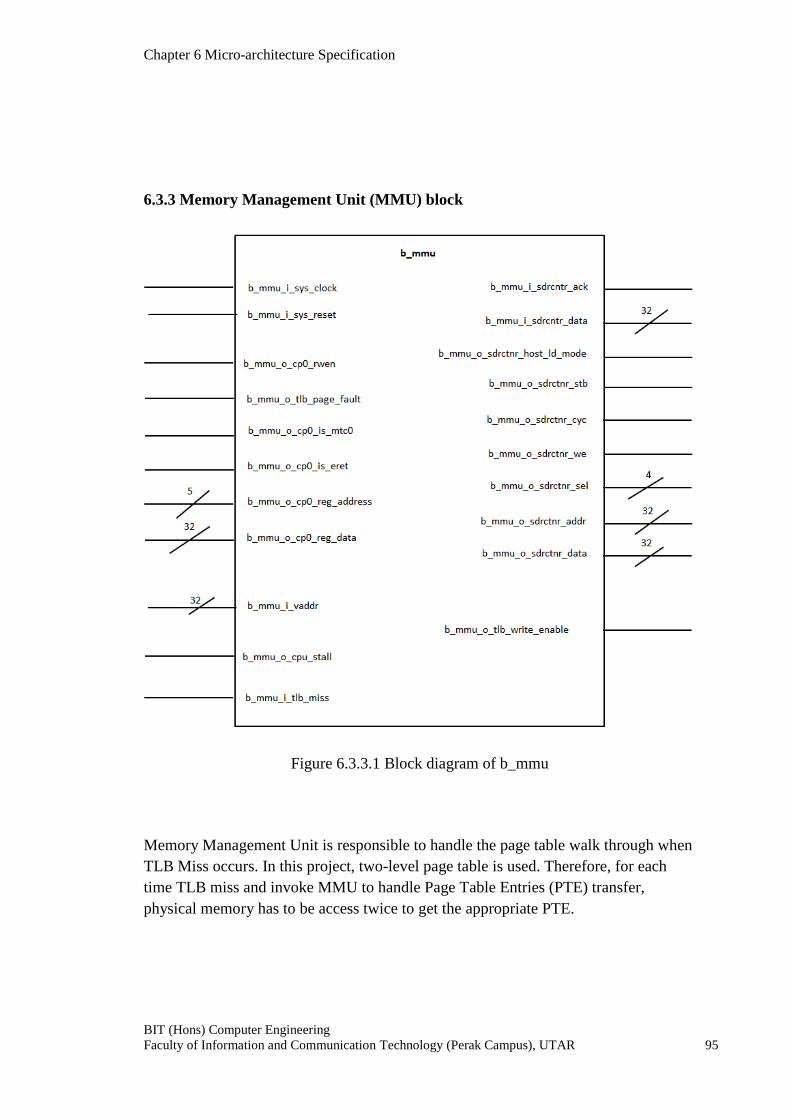
Chapter 6 Micro-architecture Specification
BIT (Hons) Computer Engineering
Faculty of Information and Communication Technology (Perak Campus), UTAR 95
6.3.3 Memory Management Unit (MMU) block
Figure 6.3.3.1 Block diagram of b_mmu
Memory Management Unit is responsible to handle the page table walk through when
TLB Miss occurs. In this project, two-level page table is used. Therefore, for each
time TLB miss and invoke MMU to handle Page Table Entries (PTE) transfer,
physical memory has to be access twice to get the appropriate PTE.

Chapter 6 Micro-architecture Specification
BIT (Hons) Computer Engineering
Faculty of Information and Communication Technology (Perak Campus), UTAR 96
6.3.3.1 I/O Description
6.3.3.1.1 Input Pins
Pin Name:
b_mmu_i_sdrctnr_ack
Source Destination:
SDRAM Controller
MMU
Registered:
No
Pin Function:
Acknowledge signal (active HIGH) to indicate read or write to SDRAM is done.
Pin Name:
b_mmu_i_sdrctnr_data[31:0]
Source Destination:
SDRAM Controller
MMU
Registered:
No
Pin Function:
32-bits data that read from SDRAM.
Pin Name:
b_mmu_i_vaddr[31:0]
Source Destination:
SDRAM Controller
MMU
Registered:
No
Pin Function:
32-bits virtual address from CPU.
Pin Name:
b_mmu_i_tlb_miss
Source Destination:
TLB Datapath MMU
Registered:
No
Pin Function:
Indicates TLB miss when HIGH
Pin Name:
b_mmu_i_sys_clock
Source Destination:
External MMU
Registered:
No
Pin Function:
System clock signal.
Pin Name:
b_mmu_i_sys_reset
Source Destination:
External MMU
Registered:
No
Pin Function:
System reset signal.
Table 6.3.3.1.1.1 MMU‟s input pin description

Chapter 6 Micro-architecture Specification
BIT (Hons) Computer Engineering
Faculty of Information and Communication Technology (Perak Campus), UTAR 97
6.3.3.1.2 Output Pins
Pin Name:
b_mmu_o_tlb_page_fault
Source Destination:
MMU CP0
Registered:
No
Pin Function:
When HIGH, indicates page fault happened.
Pin Name:
b_mmu_o_tlb_write_enable
Source Destination:
MMU TLB Datapath
Registered:
No
Pin Function:
Enables the update of the entries of TLB when HIGH.
Pin Name:
b_mmu_o_cp0_rwen
Source Destination:
MMU CP0
Registered:
No
Pin Function:
When HIGH, it indicates the TLB wants to access CP0.
Pin Name:
b_mmu_o_cp0_is_mtc0
Source Destination:
MMU CP0
Registered:
No
Pin Function:
Write enable signal to CP0.
0: Write Disable.
1: Write Enable.
Pin Name:
b_mmu_o_cp0_is_eret
Source Destination:
MMU CP0
Registered:
No
Pin Function:
Restart instruction signal for CP0.
0: Normal operation.
1: Restart exception instruction.
Pin Name:
b_mmu_o_cp0_reg_address[4:0]
Source Destination:
MMU CP0
Registered:
No
Pin Function:
5 bits address to indicate which register of CP0 should be update.

Chapter 6 Micro-architecture Specification
BIT (Hons) Computer Engineering
Faculty of Information and Communication Technology (Perak Campus), UTAR 98
Pin Name:
b_mmu_o_cp0_reg_data[31:0]
Source Destination:
MMU CP0
Registered:
No
Pin Function:
32 bits data to be written into CP0 register.
Pin Name:
b_mmu_o_cpu_stall
Source Destination:
MMU CPU
Registered:
No
Pin Function:
Control signal to stall the pipelines.
Pin Name:
b_mmu_o_sdrctnr_host_ld_mode
Source Destination:
MMU SDRAM
Controller
Registered:
No
Pin Function:
Host load mode, assert it (HIGH) to configure the operating mode in SDRAM.
Pin Name:
b_mmu_o_sdrctnr_stb
Source Destination:
MMU SDRAM
Controller
Registered:
No
Pin Function:
Strobe signal that goes to SDRAM Controller.
Pin Name:
b_mmu_o_sdrctnr_cyc
Source Destination:
MMU SDRAM
Controller
Registered:
No
Pin Function:
Cycle signal that goes to SDRAM Controller.
Pin Name:
b_mmu_o_sdrctnr_we
Source Destination:
MMU SDRAM
Controller
Registered:
No
Pin Function:
Write signal that goes to SDRAM Controller.
1 – Write
0 – Read
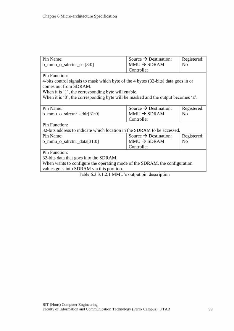
Chapter 6 Micro-architecture Specification
BIT (Hons) Computer Engineering
Faculty of Information and Communication Technology (Perak Campus), UTAR 99
Pin Name:
b_mmu_o_sdrctnr_sel[3:0]
Source Destination:
MMU SDRAM
Controller
Registered:
No
Pin Function:
4-bits control signals to mask which byte of the 4 bytes (32-bits) data goes in or
comes out from SDRAM.
When it is „1‟, the corresponding byte will enable.
When it is „0‟, the corresponding byte will be masked and the output becomes „z‟.
Pin Name:
b_mmu_o_sdrctnr_addr[31:0]
Source Destination:
MMU SDRAM
Controller
Registered:
No
Pin Function:
32-bits address to indicate which location in the SDRAM to be accessed.
Pin Name:
b_mmu_o_sdrctnr_data[31:0]
Source Destination:
MMU SDRAM
Controller
Registered:
No
Pin Function:
32-bits data that goes into the SDRAM.
When wants to configure the operating mode of the SDRAM, the configuration
values goes into SDRAM via this port too.
Table 6.3.3.1.2.1 MMU‟s output pin description

Chapter 6 Micro-architecture Specification
BIT (Hons) Computer Engineering
Faculty of Information and Communication Technology (Perak Campus), UTAR 100
6.3.4 TLB Datapath Block
Figure 6.3.4.1 Block diagram of b_tlb_dp

Chapter 6 Micro-architecture Specification
BIT (Hons) Computer Engineering
Faculty of Information and Communication Technology (Perak Campus), UTAR 101
Functionalities of TLB Datapath:
1. Compare the virtual page number (VPN) of the input virtual address with the
VPNs in all the entries in TLB to produce hit or miss signals.
2. Translate virtual address into physical address.
3. Update new page table entries from SDRAM.
6.3.4.1 I/O Description
6.3.4.1.1 Input Pins
Pin Name:
b_tlb_dp_i_vaddr[31:0]
Source Destination:
CPU TLB Datapath
Registered:
No
Pin Function:
32-bits virtual address from CPU.
Pin Name:
b_tlb_dp_i_cp0_entrylo[31:0]
Source Destination:
CP0 TLB Datapath
Registered:
No
Pin Function:
32-bits data that comes from the EntryLo register of CP0.
Pin Name:
b_tlb_dp_i_cp0_entryhi[31:0]
Source Destination:
CP0 TLB Datapath
Registered:
No
Pin Function:
32-bits data that comes from the EntryHi register of CP0.
Pin Name:
b_tlb_dp_i_cp0_random[31:0]
Source Destination:
CP0 TLB Datapath
Registered:
No
Pin Function:
32-bits data that come from the random register of CP0.
Pin Name:
b_tlb_dp_i_cp0_status[31:0]
Source Destination:
CP0 TLB Datapath
Registered:
No
Pin Function:
32-bits data that comes from status register of CP0.

Chapter 6 Micro-architecture Specification
BIT (Hons) Computer Engineering
Faculty of Information and Communication Technology (Perak Campus), UTAR 102
Pin Name:
b_tlb_dp_i_cp0_baddr[31:0]
Source Destination:
CP0 TLB Datapath
Registered:
No
Pin Function:
32-bits data that comes from baddr register of CP0.
Pin Name:
b_tlb_dp_i_wr_en
Source Destination:
MMU TLB Datapath
Registered:
No
Pin Function:
Enables the update of the entries of TLB when HIGH.
Pin Name:
b_tlb_dp_i_cpu_read
Source Destination:
CPU TLB Datapath
Registered:
No
Pin Function:
READ signal from CPU, to instruct the cache to output the value at desired location.
Pin Name:
b_tlb_dp_i_cpu_write
Source Destination:
CPU TLB Datapath
Registered:
No
Pin Function:
WRITE signal from CPU, to instruct the cache to write the input data from CPU into
the data ram.
Pin Name:
b_tlb_dp_i_rst
Source Destination:
External TLB
Datapath
Registered:
No
Pin Function:
System reset signal.
Pin Name:
b_tlb_dp_i_clk
Source Destination:
External TLB
Datapath
Registered:
No
Pin Function:
System clock signal.
Table 6.3.4.1.1.1 TLB Datapath‟s input pin description

Chapter 6 Micro-architecture Specification
BIT (Hons) Computer Engineering
Faculty of Information and Communication Technology (Perak Campus), UTAR 103
6.3.4.1.2 Output Pins
Pin Name:
b_tlb_dp_o_paddr[31:0]
Source Destination:
TLB Datapath CPU
Registered:
No
Pin Function:
32-bits translated physical address.
Pin Name:
b_tlb_dp_o_miss
Source Destination:
TLB Datapath CPU
Registered:
No
Pin Function:
When HIGH, indicates the miss in TLB.
Pin Name:
b_tlb_dp_o_addr_exception
Source Destination:
TLB Datapath CPU
Registered:
No
Pin Function:
When HIGH, indicates address exception happened.
Table 6.3.4.1.2.1 TLB Datapath‟s output pin description

Chapter 6 Micro-architecture Specification
BIT (Hons) Computer Engineering
Faculty of Information and Communication Technology (Perak Campus), UTAR 104
6.4 Memory Arbiter Block
Figure 6.4.0.1 Block diagram of b_mem_arbiter
Functionalities of memory Arbiter:
1. Decides which of the i_TLB, d_TLB, i_Cache and d_Cache get to access the
SDRAM first.
2. They all have different priority, from highest priority to lowest priority are
d_TLB, i_TLB, d_Cache and i_Cache.

Chapter 6 Micro-architecture Specification
BIT (Hons) Computer Engineering
Faculty of Information and Communication Technology (Perak Campus), UTAR 105
6.4.1 I/O Description
6.4.1.1 Input Pins
Pin Name:
b_mem_arbtr_i_stb[3:0]
Source Destination:
TLB or Cache
Memory Arbiter
Registered:
No
Pin Function:
Strobe signals from the TLBs and Caches.
Pin Name:
b_mem_arbtr_i_cyc[3:0]
Source Destination:
TLB or Cache
Memory Arbiter
Registered:
No
Pin Function:
Cycle signals from the TLBs and Caches.
Pin Name:
b_mem_arbtr_i_we[3:0]
Source Destination:
TLB or Cache
Memory Arbiter
Registered:
No
Pin Function:
READ or WRITE signals from the TLBs and Caches.
Pin Name:
b_mem_arbtr_i_host_ld_mode[3:0]
Source Destination:
TLB or Cache
Memory Arbiter
Registered:
No
Pin Function:
Host Load Mode signals from the TLBs and Caches.
Pin Name:
b_mem_arbtr_i_sel[15:0]
Source Destination:
TLB or Cache
Memory Arbiter
Registered:
No
Pin Function:
Byte Select signals from the TLBs and Caches.
Pin Name:
b_mem_arbtr_i_addr[127:0]
Source Destination:
TLB or Cache
Memory Arbiter
Registered:
No
Pin Function:
Addresses from the TLBs and Caches.

Chapter 6 Micro-architecture Specification
BIT (Hons) Computer Engineering
Faculty of Information and Communication Technology (Perak Campus), UTAR 106
Pin Name:
b_mem_arbtr_i_data[127:0]
Source Destination:
TLB or Cache
Memory Arbiter
Registered:
No
Pin Function:
Data from the TLBs and Caches.
Pin Name:
b_mem_arbtr_i_miss[3:0]
Source Destination:
TLB or Cache
Memory Arbiter
Registered:
No
Pin Function:
Miss signals from the TLBs and Caches.
Pin Name:
b_mem_arbtr_i_sdrctnr_ack
Source Destination:
SDRAM Controller
Memory Arbiter
Registered:
No
Pin Function:
Acknowledge signal (active HIGH) to indicate read or write to SDRAM is done.
Pin Name:
b_mem_arbtr_i_sdrctnr_data[31:0]
Source Destination:
SDRAM Controller
Memory Arbiter
Registered:
No
Pin Function:
32-bits data that comes from SDRAM.
Table 6.4.1.1.1 Memory Arbiter‟s input pin description
6.4.1.2 Output Pins
Pin Name:
b_mem_arbtr_o_sdrctnr_stb
Source Destination:
Memory Arbiter
SDRAM Controller
Registered:
No
Pin Function:
Strobe signal that goes to SDRAM Controller
.
Pin Name:
b_mem_arbtr_o_sdrctnr_cyc
Source Destination:
Memory Arbiter
SDRAM Controller
Registered:
No
Pin Function:
Cycle signal that goes to SDRAM Controller.
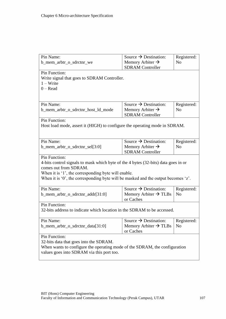
Chapter 6 Micro-architecture Specification
BIT (Hons) Computer Engineering
Faculty of Information and Communication Technology (Perak Campus), UTAR 107
Pin Name:
b_mem_arbtr_o_sdrctnr_we
Source Destination:
Memory Arbiter
SDRAM Controller
Registered:
No
Pin Function:
Write signal that goes to SDRAM Controller.
1 – Write
0 – Read
Pin Name:
b_mem_arbtr_o_sdrctnr_host_ld_mode
Source Destination:
Memory Arbiter
SDRAM Controller
Registered:
No
Pin Function:
Host load mode, assert it (HIGH) to configure the operating mode in SDRAM.
Pin Name:
b_mem_arbtr_o_sdrctnr_sel[3:0]
Source Destination:
Memory Arbiter
SDRAM Controller
Registered:
No
Pin Function:
4-bits control signals to mask which byte of the 4 bytes (32-bits) data goes in or
comes out from SDRAM.
When it is „1‟, the corresponding byte will enable.
When it is „0‟, the corresponding byte will be masked and the output becomes „z‟.
Pin Name:
b_mem_arbtr_o_sdrctnr_addr[31:0]
Source Destination:
Memory Arbiter TLBs
or Caches
Registered:
No
Pin Function:
32-bits address to indicate which location in the SDRAM to be accessed.
Pin Name:
b_mem_arbtr_o_sdrctnr_data[31:0]
Source Destination:
Memory Arbiter TLBs
or Caches
Registered:
No
Pin Function:
32-bits data that goes into the SDRAM.
When wants to configure the operating mode of the SDRAM, the configuration
values goes into SDRAM via this port too.

Chapter 6 Micro-architecture Specification
BIT (Hons) Computer Engineering
Faculty of Information and Communication Technology (Perak Campus), UTAR 108
Pin Name:
b_mem_arbtr_o_ack[3:0]
Source Destination:
Memory Arbiter
SDRAM Controller
Registered:
No
Pin Function:
Acknowledge signals (active HIGH) to indicate read or write to SDRAM is done.
Pin Name:
b_mem_arbtr_o_data[127:0]
Source Destination:
Memory Arbiter
SDRAM Controller
Registered:
No
Pin Function:
Data that read from SDRAM.
Table 6.4.1.2.1 Memory Arbiter‟s output pin description

Chapter 6 Micro-architecture Specification
BIT (Hons) Computer Engineering
Faculty of Information and Communication Technology (Perak Campus), UTAR 109
6.5 CP0 Multiplexer Block
Figure 6.5.0.1 Block diagram of b_cp0_mux

Chapter 6 Micro-architecture Specification
BIT (Hons) Computer Engineering
Faculty of Information and Communication Technology (Perak Campus), UTAR 110
Functionalities of CP0 Multiplexer:
1. Decides which of the i_TLB and d_TLB get to access the CP0 first.
2. d_TLB has higher priority over i_TLB.
6.5.1 I/O Description
6.5.1.1 Input Pins
Pin Name:
b_cp0_mux_i_itlb_cp0_rwen
Source Destination:
I_TLB CP0
Multiplexer
Registered:
No
Pin Function:
When HIGH, it indicates the i_TLB wants to access CP0.
Pin Name:
b_cp0_mux_i_itlb_tlb_miss
Source Destination:
I_TLB CP0
Multiplexer
Registered:
No
Pin Function:
Indicates i_TLB miss when HIGH
Pin Name:
b_cp0_mux_i_itlb_page_fault
Source Destination:
I_TLB CP0
Multiplexer
Registered:
No
Pin Function:
When HIGH, indicates page fault happened in i_TLB.
Pin Name:
b_cp0_mux_i_itlb_addr_exception
Source Destination:
I_TLB CP0
Multiplexer
Registered:
No
Pin Function:
When HIGH, indicates address exception happened in i_TLB.
Pin Name:
b_cp0_mux_i_itlb_is_mtc0
Source Destination:
I_TLB CP0
Multiplexer
Registered:
No
Pin Function:
Write enable signal to CP0 from i_TLB.
0: Write Disable.
1: Write Enable.

Chapter 6 Micro-architecture Specification
BIT (Hons) Computer Engineering
Faculty of Information and Communication Technology (Perak Campus), UTAR 111
Pin Name:
b_cp0_mux_i_itlb_is_eret
Source Destination:
I_TLB CP0
Multiplexer
Registered:
No
Pin Function:
1 bit signal to indicate end of i_TLB miss by sending the signal to CP0 and CP0 will
restart the instruction by loading address store in EPC register.
Pin Name:
b_cp0_mux_i_itlb_reg_address[4:0]
Source Destination:
I_TLB CP0
Multiplexer
Registered:
No
Pin Function:
5 bits register address to be update from i_TLB.
Pin Name:
b_cp0_mux_i_itlb_reg_data[31:0]
Source Destination:
I_TLB CP0
Multiplexer
Registered:
No
Pin Function:
32 bits register data to be update in CP0 register file from i_TLB
Pin Name:
b_cp0_mux_i_dtlb_ cp0_rwen
Source Destination:
D_TLB CP0
Multiplexer
Registered:
No
Pin Function:
When HIGH, it indicates the d_TLB wants to access CP0.
Pin Name:
b_cp0_mux_i_dtlb_ tlb_miss
Source Destination:
D_TLB CP0
Multiplexer
Registered:
No
Pin Function:
Indicates d_TLB miss when HIGH
Pin Name:
b_cp0_mux_i_dtlb_ page_fault
Source Destination:
D_TLB CP0
Multiplexer
Registered:
No
Pin Function:
When HIGH, indicates page fault happened in d_TLB.
Pin Name:
b_cp0_mux_i_dtlb_ addr_exception
Source Destination:
D_TLB CP0
Multiplexer
Registered:
No
Pin Function:
When HIGH, indicates address exception happened in d_TLB.
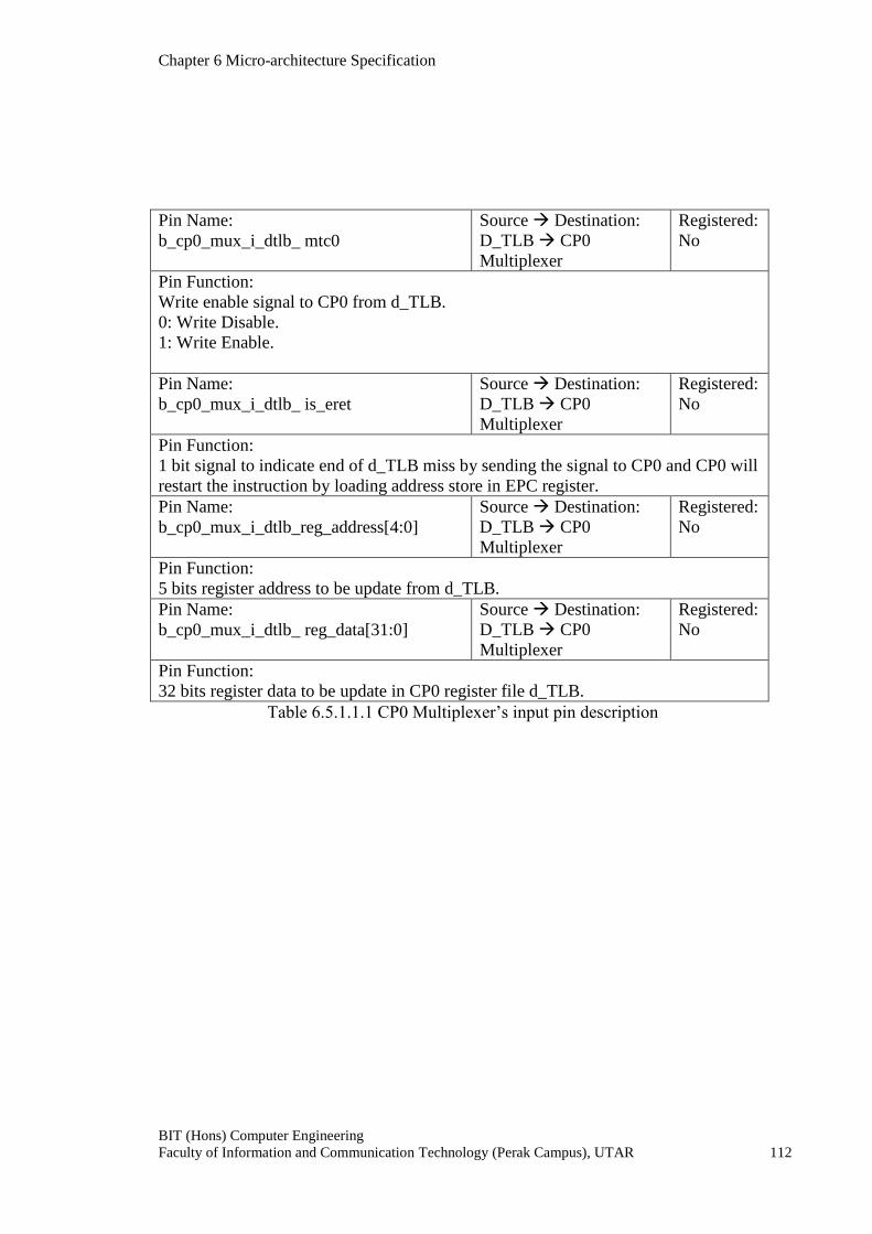
Chapter 6 Micro-architecture Specification
BIT (Hons) Computer Engineering
Faculty of Information and Communication Technology (Perak Campus), UTAR 112
Pin Name:
b_cp0_mux_i_dtlb_ mtc0
Source Destination:
D_TLB CP0
Multiplexer
Registered:
No
Pin Function:
Write enable signal to CP0 from d_TLB.
0: Write Disable.
1: Write Enable.
Pin Name:
b_cp0_mux_i_dtlb_ is_eret
Source Destination:
D_TLB CP0
Multiplexer
Registered:
No
Pin Function:
1 bit signal to indicate end of d_TLB miss by sending the signal to CP0 and CP0 will
restart the instruction by loading address store in EPC register.
Pin Name:
b_cp0_mux_i_dtlb_reg_address[4:0]
Source Destination:
D_TLB CP0
Multiplexer
Registered:
No
Pin Function:
5 bits register address to be update from d_TLB.
Pin Name:
b_cp0_mux_i_dtlb_ reg_data[31:0]
Source Destination:
D_TLB CP0
Multiplexer
Registered:
No
Pin Function:
32 bits register data to be update in CP0 register file d_TLB.
Table 6.5.1.1.1 CP0 Multiplexer‟s input pin description

Chapter 6 Micro-architecture Specification
BIT (Hons) Computer Engineering
Faculty of Information and Communication Technology (Perak Campus), UTAR 113
6.5.1.2 Output Pins
Pin Name:
b_cp0_mux_o_ tlb_miss
Source Destination:
CP0 Multiplexer CP0
Registered:
No
Pin Function:
Indicates TLB miss when HIGH
Pin Name:
b_cp0_mux_o_ page_fault
Source Destination:
CP0 Multiplexer CP0
Registered:
No
Pin Function:
When HIGH, indicates address exception happened.
Pin Name:
b_cp0_mux_o_ addr_exception
Source Destination:
CP0 Multiplexer CP0
Registered:
No
Pin Function:
When HIGH, indicates address exception happened.
Pin Name:
b_cp0_mux_o_ mtc0
Source Destination:
CP0 Multiplexer CP0
Registered:
No
Pin Function:
Write enable signal to CP0.
0: Write Disable.
1: Write Enable.
Pin Name:
b_cp0_mux_o_ is_eret
Source Destination:
CP0 Multiplexer CP0
Registered:
No
Pin Function:
1 bit signal to indicate end of TLB miss by sending the signal to CP0 and CP0 will
restart the instruction by loading address store in EPC register.

Chapter 6 Micro-architecture Specification
BIT (Hons) Computer Engineering
Faculty of Information and Communication Technology (Perak Campus), UTAR 114
Pin Name:
b_cp0_mux_o_reg_address[4:0]
Source Destination:
CP0 Multiplexer CP0
Registered:
No
Pin Function:
5 bits register address to be update.
Pin Name:
b_cp0_mux_o_ reg_data[31:0]
Source Destination:
CP0 Multiplexer CP0
Registered:
No
Pin Function:
32 bits register data to be update in CP0 register file.
Table 6.5.1.2.1 CP0 Multiplexer‟s output pin description

Chapter 7 Test and Verification
BIT (Hons) Computer Engineering
Faculty of Information and Communication Technology (Perak Campus), UTAR 115
Chapter 7: Test and Verification
7.1 Test Plan
Data is loaded into the SDRAM by $readmemh to setup the environment for testing:
Figure 7.1.1 Test plan for Memory System
The value of pc and CPU address is set to 0x0040_0000 and 0x1000_000 respectively,
then let the system runs. Expected results should be as shown in the above figure.
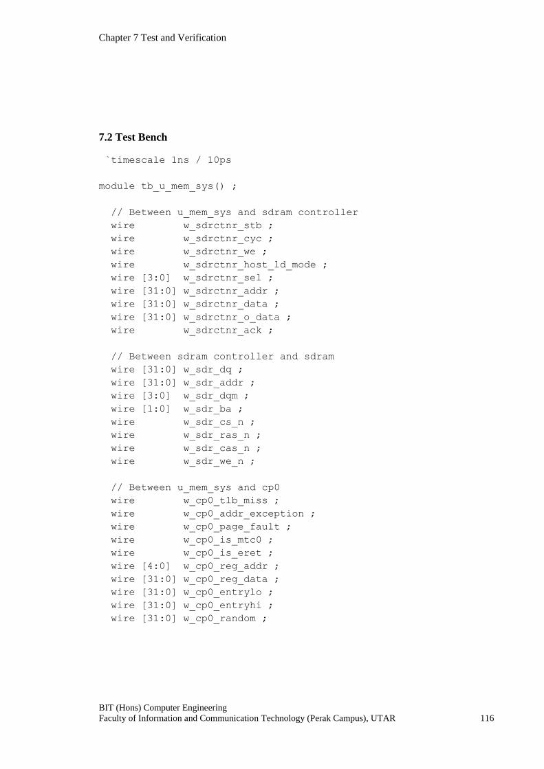
Chapter 7 Test and Verification
BIT (Hons) Computer Engineering
Faculty of Information and Communication Technology (Perak Campus), UTAR 116
7.2 Test Bench
`timescale 1ns / 10ps
module tb_u_mem_sys() ;
// Between u_mem_sys and sdram controller
wire w_sdrctnr_stb ;
wire w_sdrctnr_cyc ;
wire w_sdrctnr_we ;
wire w_sdrctnr_host_ld_mode ;
wire [3:0] w_sdrctnr_sel ;
wire [31:0] w_sdrctnr_addr ;
wire [31:0] w_sdrctnr_data ;
wire [31:0] w_sdrctnr_o_data ;
wire w_sdrctnr_ack ;
// Between sdram controller and sdram
wire [31:0] w_sdr_dq ;
wire [31:0] w_sdr_addr ;
wire [3:0] w_sdr_dqm ;
wire [1:0] w_sdr_ba ;
wire w_sdr_cs_n ;
wire w_sdr_ras_n ;
wire w_sdr_cas_n ;
wire w_sdr_we_n ;
// Between u_mem_sys and cp0
wire w_cp0_tlb_miss ;
wire w_cp0_addr_exception ;
wire w_cp0_page_fault ;
wire w_cp0_is_mtc0 ;
wire w_cp0_is_eret ;
wire [4:0] w_cp0_reg_addr ;
wire [31:0] w_cp0_reg_data ;
wire [31:0] w_cp0_entrylo ;
wire [31:0] w_cp0_entryhi ;
wire [31:0] w_cp0_random ;

Chapter 7 Test and Verification
BIT (Hons) Computer Engineering
Faculty of Information and Communication Technology (Perak Campus), UTAR 117
wire [31:0] w_cp0_status ;
wire [31:0] w_cp0_baddr ;
// cp0
wire [31:0] tb_w_cp0_reg_data ;
wire [31:0] tb_w_cp0_excep_handler_addr ;
wire tb_w_cp0_is_intr ;
wire tb_w_cp0_is_overflow ;
// Between u_mem_sys and cpu
wire [31:0] tb_w_o_cpu_instr ;
wire [31:0] tb_w_o_cpu_data ;
wire tb_w_o_cpu_stall ;
reg [31:0] tb_r_i_cpu_pc ;
reg [31:0] tb_r_i_cpu_data ;
reg [31:0] tb_r_i_cpu_addr ;
reg tb_r_i_cpu_re ;
reg tb_r_i_cpu_wr ;
// Global signals
reg tb_r_clk ;
reg tb_r_rst ;
u_cp0 cp0
(.u_cp0_i_mtc0(w_cp0_is_mtc0),
.u_cp0_i_is_eret(w_cp0_is_eret),
.u_cp0_i_current_pc_2_EPC(tb_r_i_cpu_pc),
.u_cp0_i_intr_vector(6'b0),
.u_cp0_i_overflow_signal(1'b0),
.u_cp0_i_reg_data(w_cp0_reg_data),
.u_cp0_i_reg_address(w_cp0_reg_addr),
.u_cp0_i_tlb_miss(w_cp0_tlb_miss),
.u_cp0_i_tlb_addr_excep(w_cp0_addr_exception),
.u_cp0_i_page_fault(w_cp0_page_fault),
.u_cp0_i_sys_clock(tb_r_clk),
.u_cp0_reg_i_sys_reset(tb_r_rst),
.u_cp0_o_cp0_reg_data(tb_w_cp0_reg_data),
.u_cp0_o_excep_handler_address(tb_w_cp0_excep_handler_addr),
.u_cp0_o_is_intr(tb_w_cp0_is_intr),

Chapter 7 Test and Verification
BIT (Hons) Computer Engineering
Faculty of Information and Communication Technology (Perak Campus), UTAR 118
.u_cp0_o_is_overflow(tb_w_cp0_is_overflow),
.u_cp0_o_entryLo_reg_data(w_cp0_entrylo),
.u_cp0_o_entryHi_reg_data(w_cp0_entryhi),
.u_cp0_o_random_reg_data(w_cp0_random),
.u_cp0_o_baddr_reg_data(w_cp0_baddr),
.u_cp0_o_status_reg_data(w_cp0_status) ) ;
u_mem_sys DUT
(.u_mem_sys_o_sdrctnr_stb(w_sdrctnr_stb),
.u_mem_sys_o_sdrctnr_cyc(w_sdrctnr_cyc),
.u_mem_sys_o_sdrctnr_we(w_sdrctnr_we),
.u_mem_sys_o_sdrctnr_host_ld_mode(w_sdrctnr_host_ld_mode),
.u_mem_sys_o_sdrctnr_sel(w_sdrctnr_sel),
.u_mem_sys_o_sdrctnr_addr(w_sdrctnr_addr),
.u_mem_sys_o_sdrctnr_data(w_sdrctnr_data),
.u_mem_sys_o_cp0_tlb_miss(w_cp0_tlb_miss),
.u_mem_sys_o_cp0_addr_exception(w_cp0_addr_exception),
.u_mem_sys_o_cp0_page_fault(w_cp0_page_fault),
.u_mem_sys_o_cp0_is_mtc0(w_cp0_is_mtc0),
.u_mem_sys_o_cp0_is_eret(w_cp0_is_eret),
.u_mem_sys_o_cp0_reg_addr(w_cp0_reg_addr),
.u_mem_sys_o_cp0_reg_data(w_cp0_reg_data),
.u_mem_sys_o_cpu_instr(tb_w_o_cpu_instr),
.u_mem_sys_o_cpu_data(tb_w_o_cpu_data),
.u_mem_sys_o_cpu_stall(tb_w_o_cpu_stall),
.u_mem_sys_i_sdrctnr_ack(w_sdrctnr_ack),
.u_mem_sys_i_sdrctnr_data(w_sdrctnr_o_data),
.u_mem_sys_i_cp0_entrylo(w_cp0_entrylo),
.u_mem_sys_i_cp0_entryhi(w_cp0_entryhi),
.u_mem_sys_i_cp0_random(w_cp0_random),
.u_mem_sys_i_cp0_status(w_cp0_status),
.u_mem_sys_i_cp0_baddr(w_cp0_baddr),
.u_mem_sys_i_cpu_pc(tb_r_i_cpu_pc),
.u_mem_sys_i_cpu_data(tb_r_i_cpu_data),
.u_mem_sys_i_cpu_addr(tb_r_i_cpu_addr),
.u_mem_sys_i_cpu_re(tb_r_i_cpu_re),
.u_mem_sys_i_cpu_wr(tb_r_i_cpu_wr),
.u_mem_sys_i_clk(tb_r_clk),

Chapter 7 Test and Verification
BIT (Hons) Computer Engineering
Faculty of Information and Communication Technology (Perak Campus), UTAR 119
.u_mem_sys_i_rst(tb_r_rst) ) ;
sdram_controller sdram_controller
(.ip_wb_clk(tb_r_clk),
.ip_wb_rst(tb_r_rst),
.ip_host_ld_mode(w_sdrctnr_host_ld_mode),
.ip_wb_stb(w_sdrctnr_stb),
.ip_wb_cyc(w_sdrctnr_cyc),
.ip_wb_we(w_sdrctnr_we),
.ip_wb_sel(w_sdrctnr_sel),
.ip_wb_addr(w_sdrctnr_addr),
.ip_wb_dat(w_sdrctnr_data),
.op_wb_dat(w_sdrctnr_o_data),
.op_wb_ack(w_sdrctnr_ack),
.io_sdr_dq(w_sdr_dq),
.op_sdr_ba(w_sdr_ba),
.op_sdr_dqm(w_sdr_dqm),
.op_sdr_addr(w_sdr_addr),
.op_sdr_cs_n(w_sdr_cs_n),
.op_sdr_ras_n(w_sdr_ras_n),
.op_sdr_cas_n(w_sdr_cas_n),
.op_sdr_we_n(w_sdr_we_n) ) ;
mt48lc4m32b2 SDRAM
(.Dq(w_sdr_dq),
.Addr(w_sdr_addr),
.Ba(w_sdr_ba),
.Clk(tb_r_clk),
.Cke(1'b1),
.Cs_n(w_sdr_cs_n),
.Ras_n(w_sdr_ras_n),
.Cas_n(w_sdr_cas_n),
.We_n(w_sdr_we_n),
.Dqm(w_sdr_dqm) ) ;
initial tb_r_clk = 0 ;
always #20 tb_r_clk = ~tb_r_clk ;

Chapter 7 Test and Verification
BIT (Hons) Computer Engineering
Faculty of Information and Communication Technology (Perak Campus), UTAR 120
initial begin
tb_r_i_cpu_pc = 32'h0040_0000 ;
tb_r_i_cpu_data = 32'h0000_0000 ;
tb_r_i_cpu_addr = 32'h0000_0000 ;
tb_r_i_cpu_re = 1'b0 ;
tb_r_i_cpu_wr = 1'b0 ;
tb_r_rst = 1'b1 ;
repeat(10) @(posedge tb_r_clk) ;
tb_r_rst = 1'b0 ;
// Prepare data in sdram
$readmemh("sdram_bank0_data.txt", SDRAM.Bank0) ;
// itlb and icache should miss
// wait until itlb and icache done
while(tb_w_o_cpu_stall) @(posedge tb_r_clk) ;
tb_r_i_cpu_pc = 32'h0040_0004 ; // 2nd instr comes in
@(posedge tb_r_clk)
tb_r_i_cpu_pc = 32'h0040_0008 ; // 3rd instr comes in
@(posedge tb_r_clk)
tb_r_i_cpu_pc = 32'h0040_000C ; // 4th instr comes in
// MEM stage
// Read a data from 0x1000_000
tb_r_i_cpu_data = 32'h0000_0000 ;
tb_r_i_cpu_addr = 32'h1000_0000 ;
tb_r_i_cpu_re = 1'b1 ;
tb_r_i_cpu_wr = 1'b0 ;
@(posedge tb_r_clk) ;
// Expecting dtlb and dcache misses
// Wait until they are done
while(tb_w_o_cpu_stall) @(posedge tb_r_clk) ;
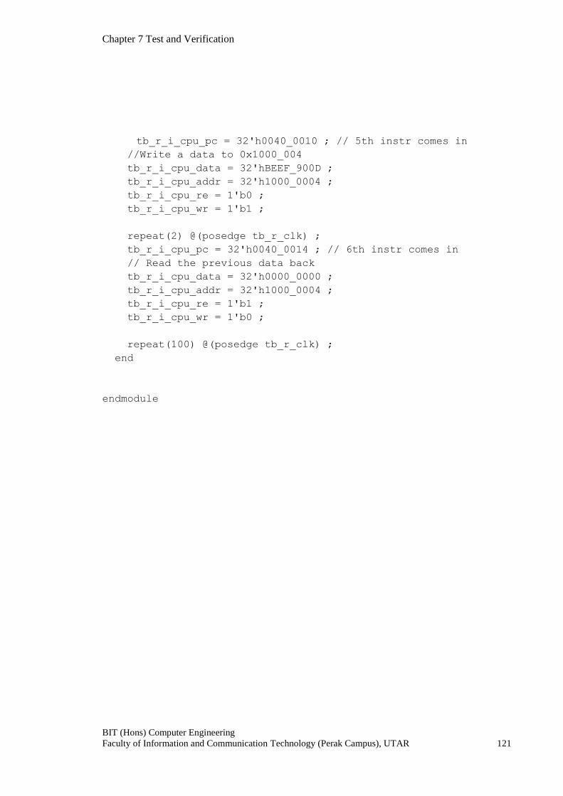
Chapter 7 Test and Verification
BIT (Hons) Computer Engineering
Faculty of Information and Communication Technology (Perak Campus), UTAR 121
tb_r_i_cpu_pc = 32'h0040_0010 ; // 5th instr comes in
//Write a data to 0x1000_004
tb_r_i_cpu_data = 32'hBEEF_900D ;
tb_r_i_cpu_addr = 32'h1000_0004 ;
tb_r_i_cpu_re = 1'b0 ;
tb_r_i_cpu_wr = 1'b1 ;
repeat(2) @(posedge tb_r_clk) ;
tb_r_i_cpu_pc = 32'h0040_0014 ; // 6th instr comes in
// Read the previous data back
tb_r_i_cpu_data = 32'h0000_0000 ;
tb_r_i_cpu_addr = 32'h1000_0004 ;
tb_r_i_cpu_re = 1'b1 ;
tb_r_i_cpu_wr = 1'b0 ;
repeat(100) @(posedge tb_r_clk) ;
end
endmodule

Chapter 7 Test and Verification
BIT (Hons) Computer Engineering
Faculty of Information and Communication Technology (Perak Campus), UTAR 122
7.3 Simulation Results
Figure 7.3.1 Simulation results
itlb missed, configuring the
operating mode to single
location access
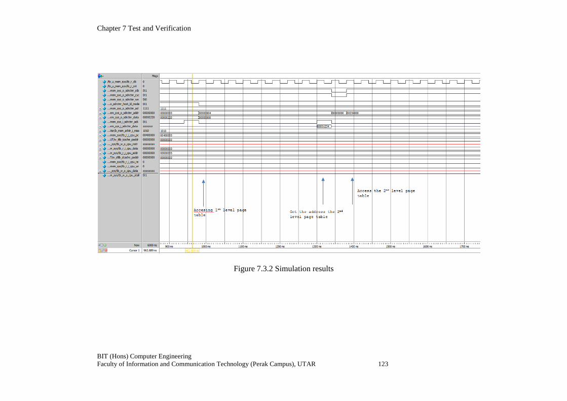
Chapter 7 Test and Verification
BIT (Hons) Computer Engineering
Faculty of Information and Communication Technology (Perak Campus), UTAR 123
Figure 7.3.2 Simulation results

Chapter 7 Test and Verification
BIT (Hons) Computer Engineering
Faculty of Information and Communication Technology (Perak Campus), UTAR 124
Figure 7.3.3 Simulation results

Chapter 7 Test and Verification
BIT (Hons) Computer Engineering
Faculty of Information and Communication Technology (Perak Campus), UTAR 125
Figure 7.3.4 Simulation results

Chapter 7 Test and Verification
BIT (Hons) Computer Engineering
Faculty of Information and Communication Technology (Perak Campus), UTAR 126
Figure 7.3.5 Simulation results

Chapter 7 Test and Verification
BIT (Hons) Computer Engineering
Faculty of Information and Communication Technology (Perak Campus), UTAR 127
Figure 7.3.6 Simulation results

Chapter 7 Test and Verification
BIT (Hons) Computer Engineering
Faculty of Information and Communication Technology (Perak Campus), UTAR 128
Figure 7.3.7 Simulation results

Chapter 7 Test and Verification
BIT (Hons) Computer Engineering
Faculty of Information and Communication Technology (Perak Campus), UTAR 129
Figure 7.3.8 Simulation results

Chapter 7 Test and Verification
BIT (Hons) Computer Engineering
Faculty of Information and Communication Technology (Perak Campus), UTAR 130
Figure 7.3.9 SRAM‟s read/write transcript

Chapter 8 Discussion and Conclusion
BIT (Hons) Computer Engineering
Faculty of Information and Communication Technology (Perak Campus), UTAR 131
Chapter 8: Discussion and Conclusion
8.1 Discussion and Conclusion
Virtual memory act as a barrier to hide the physical memory specifications
from the users and programmers. Adoption on virtual memory requires the translation
of virtual addresses to physical addresses. Translating a virtual address to physical
address will need to access its page table which is stored in main memory. Although it
might seems a little abit troublesome to translate the addresses before accessing the
memory, but virtual memory is the reason why we can have several programs running
on the system at the same time, it totally worth the effort.
Caches and Translation Lookaside Buffer (TLB) are implemented to boost up
the performance of the whole system. Without caches or TLB, the processor will have
to obtain data or instruction directly from main memory, which is probably a DRAM.
Accessing DRAM once can take up to 40 to 50 clock cycles. In this case, the
performance of the system will be limited by the memory regardless how fast the
processor is. Caches and TLBs are temporary buffers which are small but fast to hold
a small fraction of the data or instruction (for caches) and page table (for TLB) in
main memory. Reading from caches and TLB will only need one clock cycle, or
maybe two for caches, and writing to caches will have to take two to three clock
cycles only. Compare this 3 clock cycles with 50 clock cycles, what a huge boost up.
However, we will have to bear the penalties when read miss or write miss. Several
processes will have to go through in order to handle the misses.

Chapter 8 Discussion and Conclusion
BIT (Hons) Computer Engineering
Faculty of Information and Communication Technology (Perak Campus), UTAR 132
In this project, 64 entries TLBs, 2MB Caches and 16MB of SDRAM have
been successfully put together as a whole Memory System. Its behaviour has been
tested during the verification stage. Seems like it works fine, just that the cpu stall
signal working not quite well, it does not asserted when the cache write hit, which
requires 2 clock cycles. Furthermore, the test cases in the verification stage is not
complete, so we still cannot justify that the memory system is complete yet.
8.2 Future Works
The Memory System is not complete yet, but nearly. The cpu stall signal need
to be fixed and the Memory System need to be tested with complete test cases to
ensure it is working fine.
There are some enhancements that can be done on this Memory System. Add a
write buffer to the cache so that the data that is going to be written back to SDRAM
can wait, let the data requested by CPU can be fetched from SDRAM first, this will
further boost up the performance of the system. Enhance the SDRAM Controller, so
that it can control more than one SDRAM chip, the systen will have more physical
memory. Add another victim buffer to the cache, so that the data that is going to be
thrown away can stay inside, they might have another chance to be called by the CPU
again, who knows?

References
BIT (Hons) Computer Engineering
Faculty of Information and Communication Technology (Perak Campus), UTAR 131
References
[1] Mittra, S. (1995) IEEE Xplore/IEL. A Virtual Memory Management Scheme
For Simulation Enviroment, 1 (2012), p.114,115,116.
[2] JAY SMITH, A. (2010) IEEE Xplore/IEL. A Comparative Study of Set
Associative Memory Mapping Algorithms and Their Use for Cache and Main
Memory, p.121-128.
[3] Design Gateway Corporation (2002) SDRAM CONTROLLER DESIGN
MANUAL. [online] Available at: http://www.dgway.com/products/IP/IP-
SDRAMCTL.pdf [Accessed: 20 July 2012].
[4] G. Cragon, H. (1996) Memory Systems and Pipelined Processors Jones and
Bartlett Books in Computer Science. Jones & Bartlett Publishers, Inc..
[5] L. Hennessy, J. and A. Patterson , D. (2004) Computer Organization and
Design the hardware/software interface. 3rd ed. India: Morgan Kaufman
Publishers.
[6] Sweetman, D. (2012) See MIPS Run . 2nd ed. Boston: Denise E. M. Penrose.
[7] Zhi Kang Oon, “SDRAM Enhancement: Design of a SDRAM Controller
WISHBONE Industrial Standard” University of Tunku Abdul Rahman,
Faculty of Information and Communication Technology, 2008.

References
BIT (Hons) Computer Engineering
Faculty of Information and Communication Technology (Perak Campus), UTAR 132
[8] Chun Jin Teoh, “RISC32 Interrupt Handling or Enhanced RISC32
Architecture” University of Tunku Abdul Rahman, Faculty of Information and
Communication Technology, 2012.
[9] Kim Yuh Change, “Design and Development of Memory System for 32 bits 5-
stage Pipelined Processor: Main Memory (DRAM) Integration” University of
Tunku Abdul Rahman, Faculty of Information and Communication
Technology, 2013.
[10] Khoo Chong Siang, “Design and Development of Memory System for 32bit
5stage pipeline processor: I-cache and D-cache Integration” University of
Tunku Abdul Rahman, Faculty of Information and Communication
Technology, 2013.

![Hardware Translation Coherence for Virtualized Systems · the page table. Translation coherence is the means by which caches dedicated to translations (e.g., TLBs [12, 40, 50, 51],](https://img.pdfslide.us/doc/110x75/5fda468817dff94c2d646d57/hardware-translation-coherence-for-virtualized-the-page-table-translation-coherence.jpg)


![[06] PAGING - University of Cambridge · 0 OUTLINE Paged Virtual Memory Concepts Pros and Cons Page Tables Translation Lookaside Buffer (TLB) Protection & Sharing Virtual Memory Demand](https://img.pdfslide.us/doc/110x75/5acbcefa7f8b9a27628bbc9d/06-paging-university-of-cambridge-outline-paged-virtual-memory-concepts-pros.jpg)