Embed Size (px)
Citation preview
www.ti.com
FEATURES APPLICATIONS
DESCRIPTION
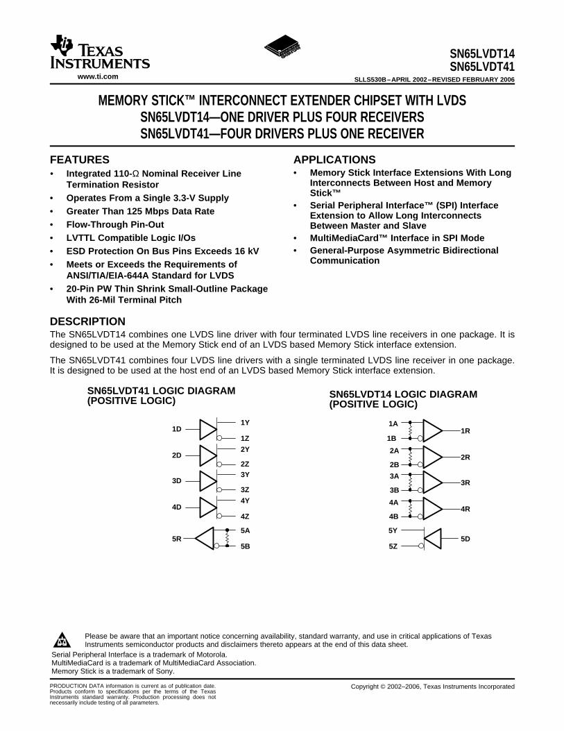
SN65LVDT14 LOGIC DIAGRAM(POSITIVE LOGIC)
SN65LVDT41 LOGIC DIAGRAM(POSITIVE LOGIC)
1Y
1Z1D
1A
1B
5Y
5Z
1R
5D
2Y
2Z2D
2A
2B2R
3Y
3Z3D
3A
3B3R
4Y
4Z4D
4A
4B4R
5A
5B5R
SN65LVDT14SN65LVDT41
SLLS530B–APRIL 2002–REVISED FEBRUARY 2006
MEMORY STICK™ INTERCONNECT EXTENDER CHIPSET WITH LVDSSN65LVDT14—ONE DRIVER PLUS FOUR RECEIVERSSN65LVDT41—FOUR DRIVERS PLUS ONE RECEIVER
• Memory Stick Interface Extensions With Long• Integrated 110-Ω Nominal Receiver LineInterconnects Between Host and MemoryTermination ResistorStick™• Operates From a Single 3.3-V Supply
• Serial Peripheral Interface™ (SPI) Interface• Greater Than 125 Mbps Data Rate Extension to Allow Long Interconnects• Flow-Through Pin-Out Between Master and Slave• LVTTL Compatible Logic I/Os • MultiMediaCard™ Interface in SPI Mode
• General-Purpose Asymmetric Bidirectional• ESD Protection On Bus Pins Exceeds 16 kVCommunication• Meets or Exceeds the Requirements of
ANSI/TIA/EIA-644A Standard for LVDS• 20-Pin PW Thin Shrink Small-Outline Package
With 26-Mil Terminal Pitch
The SN65LVDT14 combines one LVDS line driver with four terminated LVDS line receivers in one package. It isdesigned to be used at the Memory Stick end of an LVDS based Memory Stick interface extension.
The SN65LVDT41 combines four LVDS line drivers with a single terminated LVDS line receiver in one package.It is designed to be used at the host end of an LVDS based Memory Stick interface extension.
Please be aware that an important notice concerning availability, standard warranty, and use in critical applications of TexasInstruments semiconductor products and disclaimers thereto appears at the end of this data sheet.
Serial Peripheral Interface is a trademark of Motorola.MultiMediaCard is a trademark of MultiMediaCard Association.Memory Stick is a trademark of Sony.
PRODUCTION DATA information is current as of publication date. Copyright © 2002–2006, Texas Instruments IncorporatedProducts conform to specifications per the terms of the TexasInstruments standard warranty. Production processing does notnecessarily include testing of all parameters.

www.ti.com
TYPICAL MEMORY STICK INTERFACE EXTENSION
1Y
1Z1D
1A
1B
5Y
5Z
1R
5D
2Y
2Z2D 2A
2B2R
3Y
3Z3D 3A
3B3R
4Y
4Z4D 4A
4B4R
5A
5B5R
SCLK
BS
DIR
SD1
SD2
CBT
SCLK
BS
SDIO
MemoryStick
CBT
SCLK
BS
SDIO
DIR
MemoryStickHost
Controller
SN65LVDT41 SN65LVDT14
ABSOLUTE MAXIMUM RATINGS
PACKAGE DISSIPATION RATINGS
SN65LVDT14SN65LVDT41SLLS530B–APRIL 2002–REVISED FEBRUARY 2006
These devices have limited built-in ESD protection. The leads should be shorted together or the device placed in conductive foamduring storage or handling to prevent electrostatic damage to the MOS gates.
over operating free-air temperature range unless otherwise noted (1)
SN65LVDT14, UNITSN65LVDT41
Supply voltage range (2) VCC -0.5 to 4 V
D or R -0.5 to 6 VInput voltage range
A, B, Y, or Z -0.5 to 4 V
Human body model (3), A, B, Y, Z, and GND ±16 KV
Electrostatic discharge Human body model (3), all pins ±8 KV
Charged device model (4), all pins ±500 V
Continuous total power dissipation See Dissipation Rating Table
Storage temperature range -65 to 150 °C
Lead temperature 1,6 mm (1/16 inch) from case for 10 seconds 260 °C
(1) Stresses beyond those listed under absolute maximum ratings may cause permanent damage to the device. These are stress ratingsonly, and functional operation of the device at these or any other conditions beyond those indicated under recommended operatingconditions is not implied. Exposure to absolute-maximum-rated conditions for extended periods may affect device reliability.
(2) All voltage values, except differential I/O bus voltages are with respect to network ground terminal.(3) Tested in accordance with JEDEC Standard 22, Test Method A114-A.(4) Tested in accordance with JEDEC Standard 22, Test Method C101.
TA <25°C OPERATING FACTOR TA = 85°CPACKAGE POWER RATING ABOVE TA = 25°C POWER RATING
PW 774 mW 6.2 mW/°C 402 mW
2 Submit Documentation Feedback
www.ti.com
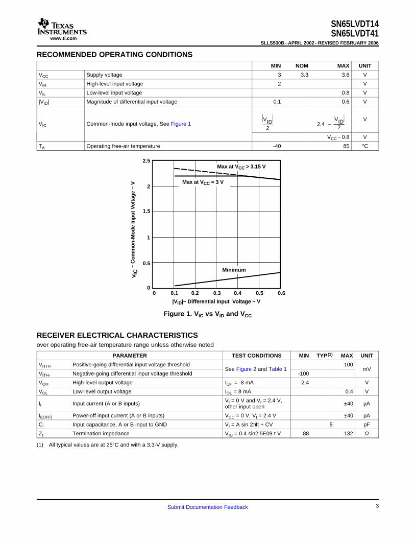
RECOMMENDED OPERATING CONDITIONS
2.4
VID
2
VID
2
|VID|− Differential Input Voltage − V
1
00.1 0.3
2
1.5
0.5
0.2 0.4 0.6
2.5
0 0.5
Max at VCC = 3 V
− C
om
mo
n-M
od
e In
pu
t Vo
ltag
e −
VV
IC
Max at VCC > 3.15 V
Minimum
RECEIVER ELECTRICAL CHARACTERISTICS
SN65LVDT14SN65LVDT41
SLLS530B–APRIL 2002–REVISED FEBRUARY 2006
MIN NOM MAX UNIT
VCC Supply voltage 3 3.3 3.6 V
VIH High-level input voltage 2 V
VIL Low-level input voltage 0.8 V
|VID| Magnitude of differential input voltage 0.1 0.6 V
VVIC Common-mode input voltage, See Figure 1
VCC - 0.8 V
TA Operating free-air temperature -40 85 °C
Figure 1. VIC vs VID and VCC
over operating free-air temperature range unless otherwise noted
PARAMETER TEST CONDITIONS MIN TYP (1) MAX UNIT
VITH+ Positive-going differential input voltage threshold 100See Figure 2 and Table 1 mV
VITH- Negative-going differential input voltage threshold -100
VOH High-level output voltage IOH = -8 mA 2.4 V
VOL Low-level output voltage IOL = 8 mA 0.4 V
VI = 0 V and VI = 2.4 V,II Input current (A or B inputs) ±40 µAother input open
II(OFF) Power-off input current (A or B inputs) VCC = 0 V, VI = 2.4 V ±40 µA
Ci Input capacitance, A or B input to GND VI = A sin 2πft + CV 5 pF
Zt Termination impedance VID = 0.4 sin2.5E09 t V 88 132 Ω
(1) All typical values are at 25°C and with a 3.3-V supply.
3Submit Documentation Feedback
www.ti.com
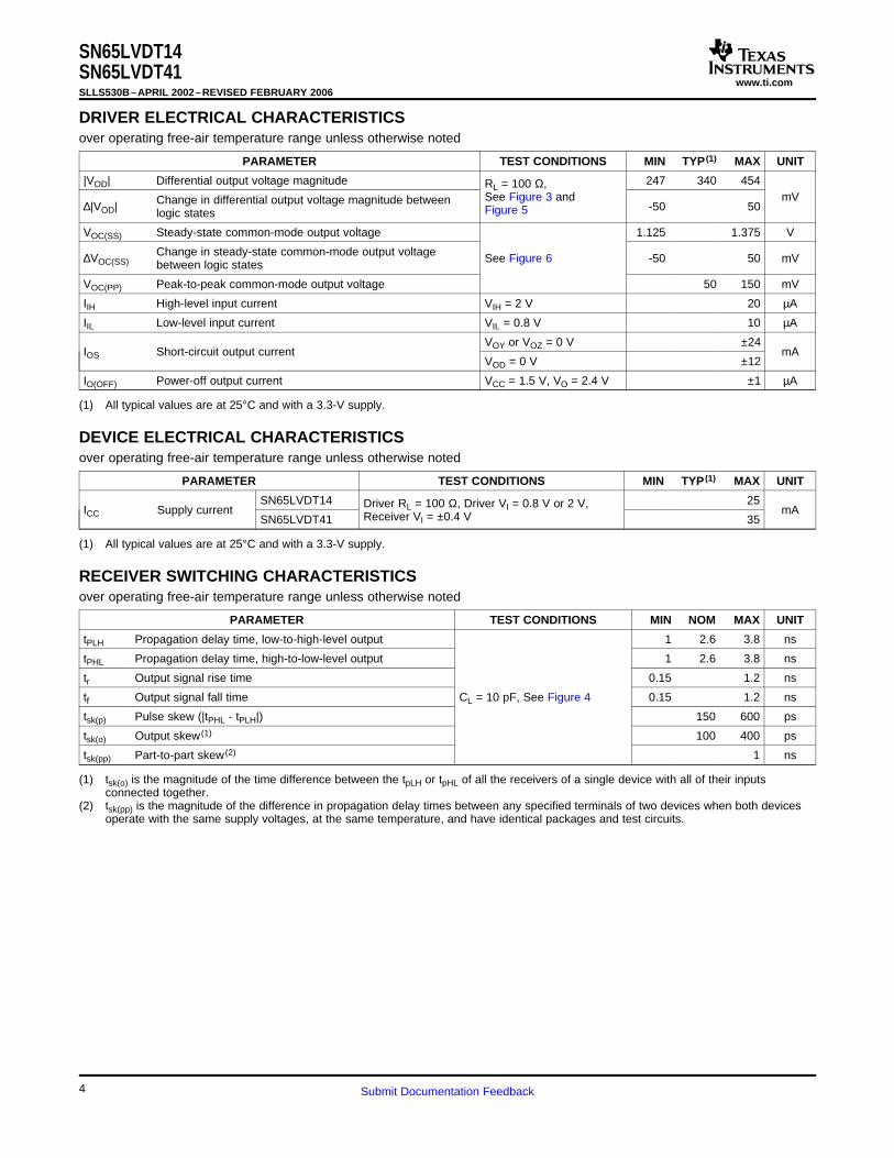
DRIVER ELECTRICAL CHARACTERISTICS
DEVICE ELECTRICAL CHARACTERISTICS
RECEIVER SWITCHING CHARACTERISTICS
SN65LVDT14SN65LVDT41SLLS530B–APRIL 2002–REVISED FEBRUARY 2006
over operating free-air temperature range unless otherwise noted
PARAMETER TEST CONDITIONS MIN TYP (1) MAX UNIT
|VOD| Differential output voltage magnitude 247 340 454RL = 100 Ω,See Figure 3 and mVChange in differential output voltage magnitude between∆|VOD| -50 50Figure 5logic states
VOC(SS) Steady-state common-mode output voltage 1.125 1.375 V
Change in steady-state common-mode output voltage∆VOC(SS) See Figure 6 -50 50 mVbetween logic states
VOC(PP) Peak-to-peak common-mode output voltage 50 150 mV
IIH High-level input current VIH = 2 V 20 µA
IIL Low-level input current VIL = 0.8 V 10 µA
VOY or VOZ = 0 V ±24IOS Short-circuit output current mA
VOD = 0 V ±12
IO(OFF) Power-off output current VCC = 1.5 V, VO = 2.4 V ±1 µA
(1) All typical values are at 25°C and with a 3.3-V supply.
over operating free-air temperature range unless otherwise noted
PARAMETER TEST CONDITIONS MIN TYP (1) MAX UNIT
SN65LVDT14 25Driver RL = 100 Ω, Driver VI = 0.8 V or 2 V,ICC Supply current mAReceiver VI = ±0.4 VSN65LVDT41 35
(1) All typical values are at 25°C and with a 3.3-V supply.
over operating free-air temperature range unless otherwise noted
PARAMETER TEST CONDITIONS MIN NOM MAX UNIT
tPLH Propagation delay time, low-to-high-level output 1 2.6 3.8 ns
tPHL Propagation delay time, high-to-low-level output 1 2.6 3.8 ns
tr Output signal rise time 0.15 1.2 ns
tf Output signal fall time CL = 10 pF, See Figure 4 0.15 1.2 ns
tsk(p) Pulse skew (|tPHL - tPLH|) 150 600 ps
tsk(o) Output skew (1) 100 400 ps
tsk(pp) Part-to-part skew (2) 1 ns
(1) tsk(o) is the magnitude of the time difference between the tpLH or tpHL of all the receivers of a single device with all of their inputsconnected together.
(2) tsk(pp) is the magnitude of the difference in propagation delay times between any specified terminals of two devices when both devicesoperate with the same supply voltages, at the same temperature, and have identical packages and test circuits.
4 Submit Documentation Feedback
www.ti.com
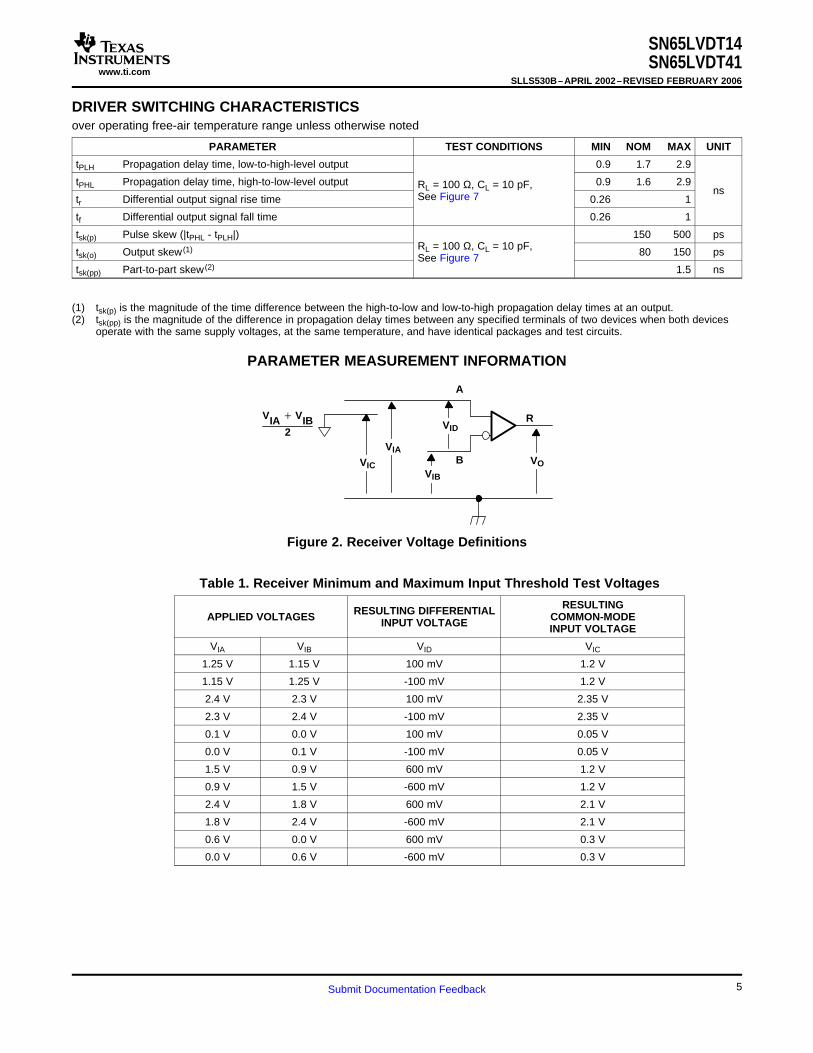
DRIVER SWITCHING CHARACTERISTICS
PARAMETER MEASUREMENT INFORMATION
VIB
VID
VIA
VIC VO
A
B
RVIA VIB2
SN65LVDT14SN65LVDT41
SLLS530B–APRIL 2002–REVISED FEBRUARY 2006
over operating free-air temperature range unless otherwise noted
PARAMETER TEST CONDITIONS MIN NOM MAX UNIT
tPLH Propagation delay time, low-to-high-level output 0.9 1.7 2.9
tPHL Propagation delay time, high-to-low-level output 0.9 1.6 2.9RL = 100 Ω, CL = 10 pF, nsSee Figure 7tr Differential output signal rise time 0.26 1
tf Differential output signal fall time 0.26 1
tsk(p) Pulse skew (|tPHL - tPLH|) 150 500 psRL = 100 Ω, CL = 10 pF,tsk(o) Output skew (1) 80 150 psSee Figure 7
tsk(pp) Part-to-part skew (2) 1.5 ns
(1) tsk(p) is the magnitude of the time difference between the high-to-low and low-to-high propagation delay times at an output.(2) tsk(pp) is the magnitude of the difference in propagation delay times between any specified terminals of two devices when both devices
operate with the same supply voltages, at the same temperature, and have identical packages and test circuits.
Figure 2. Receiver Voltage Definitions
Table 1. Receiver Minimum and Maximum Input Threshold Test Voltages
RESULTINGRESULTING DIFFERENTIALAPPLIED VOLTAGES COMMON-MODEINPUT VOLTAGE INPUT VOLTAGE
VIA VIB VID VIC
1.25 V 1.15 V 100 mV 1.2 V
1.15 V 1.25 V -100 mV 1.2 V
2.4 V 2.3 V 100 mV 2.35 V
2.3 V 2.4 V -100 mV 2.35 V
0.1 V 0.0 V 100 mV 0.05 V
0.0 V 0.1 V -100 mV 0.05 V
1.5 V 0.9 V 600 mV 1.2 V
0.9 V 1.5 V -600 mV 1.2 V
2.4 V 1.8 V 600 mV 2.1 V
1.8 V 2.4 V -600 mV 2.1 V
0.6 V 0.0 V 600 mV 0.3 V
0.0 V 0.6 V -600 mV 0.3 V
5Submit Documentation Feedback

www.ti.com
VOD
VOZ
VOY
VOCVI
IOY
IOZ
IID
Z
Y
VOY VOZ2
VIB
VID
VIAVO
CL10 pF
VOH
VOL
VCC/2
VO
VIA
VIB
VID
1.4 V
1 V
0.4 V
0 V
–0.4 V
tPHL tPLH
trtf
20%
80%
VOD 100 Ω
3.75 kΩ
3.75 kΩ
_+ 0 V ≤ Vtest ≤ 2.4 V
Y
Z
Input
SN65LVDT14SN65LVDT41SLLS530B–APRIL 2002–REVISED FEBRUARY 2006
Figure 3. Driver Voltage and Current Definitions
A. All input pulses are supplied by a generator having the following characteristics: tr or tf ≤ 1 ns, pulse repetition rate(PRR) = 1 Mpps, pulse width = 0.5 ± 0.05 µs. CL includes instrumentation and fixture capacitance within 0,06 m of theD.U.T.
Figure 4. Receiver Timing Test Circuit and Waveforms
Figure 5. Driver VDO Test Circuit
6 Submit Documentation Feedback

www.ti.com
VOC
Z
Y
Input
2 pF
3 V
0 V
VOC(PP) VOC(SS)
VOC
49.9 Ω, ±1% (2 Places)
VIA
D
2 V1.4 V0.8 V
100%
80%
20%
0%
0 V
VOD(H)
VOD(L)
Output
Input
VOD
Z
Y
Input100 Ω±1%
CL(2 Places)
tPHLtPLH
tf tr
SN65LVDT14SN65LVDT41
SLLS530B–APRIL 2002–REVISED FEBRUARY 2006
A. All input pulses are supplied by a generator having the following characteristics: tr or tf ≤ 1 ns, pulse repetition rate(PRR) = 0.5 Mpps, pulse width = 500 ± 10 ns. CL includes instrumentation and fixture capacitance within 0,06 mm ofthe D.U.T. The measurement of VOC(PP) is made on test equipment with a -3 dB bandwidth of at least 1 GHz.
Figure 6. Test Circuit and Definitions for the Driver Common-Mode Output Voltage
A. All input pulses are supplied by a generator having the following characteristics: tr or tf ≤ 1 ns, pulse repetition rate(PRR) = 1 Mpps, pulse width = 0.5 ± 0.05 µs. CL includes instrumentation and fixture capacitance within 0,06 mm ofthe D.U.T.
Figure 7. Test Circuit, Timing, and Voltage Definitions for the Differential Output Signal
7Submit Documentation Feedback
www.ti.com
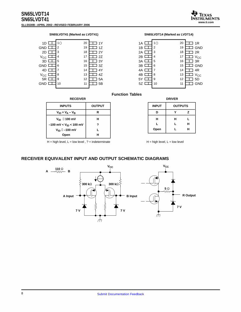
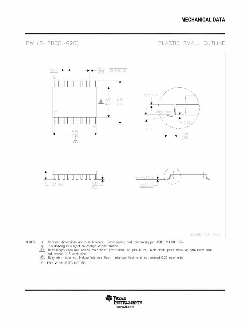
123
4 56789
10
201918
171615141312
11
1DGND
2DVCC
3DGND
4DVCC
5RGND
1Y1Z2Y2Z3Y3Z4Y4Z5A5B
SN65LVDT41 (Marked as LVDT41)
123
4 56789
10
201918
171615141312
11
1A1B2A2B3A3B4A4B5Y5Z
1RGND2RVCC3RGND4RVCC5DGND
SN65LVDT14 (Marked as LVDT14)
INPUT OUTPUTS
D
H
L
Open
Y Z
H
L
L
L
H
H
DRIVER
INPUTS OUTPUT
R
H
?
L
VID = VA – VB
VID ≥ 100 mV
–100 mV < VID < 100 mV
VID ≤ –100 mV
Open H
H = high level, L = low level
Function TablesRECEIVER
H = high level, L = low level , ? = indeterminate
RECEIVER EQUIVALENT INPUT AND OUTPUT SCHEMATIC DIAGRAMS
7 V
VCC
7 V
R Output
VCC
5 Ω
B InputA Input
300 kΩ300 kΩ
7 V
110 ΩA B
SN65LVDT14SN65LVDT41SLLS530B–APRIL 2002–REVISED FEBRUARY 2006
8 Submit Documentation Feedback
www.ti.com
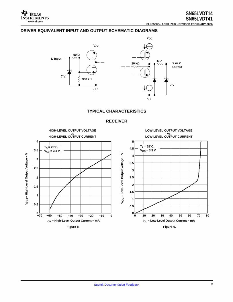
DRIVER EQUIVALENT INPUT AND OUTPUT SCHEMATIC DIAGRAMS
300 kΩ
50 Ω
VCC
7 V
D Input5 Ω
10 kΩ
7 V
Y or ZOutput
VCC
TYPICAL CHARACTERISTICS
RECEIVER
IOH − High-Level Output Current − mA
VO
H−
Hig
h-L
evel
Ou
tpu
t Vo
ltag
e −
V
4
3.5
3
2.5
2
1.5
1
0.5
0−70 −60 −50 −40 −30 −20 −10 0
TA = 25°C,VCC = 3.3 V
IOL − Low-Level Output Current − mA
OL
V−
Lo
w-L
evel
Ou
tpu
t Vo
ltag
e −
V
5
4.5
4
3.5
3
2.5
2
1.5
1
0.5
00 10 20 30 40 50 60 70 80
TA = 25°C,VCC = 3.3 V
SN65LVDT14SN65LVDT41
SLLS530B–APRIL 2002–REVISED FEBRUARY 2006
HIGH-LEVEL OUTPUT VOLTAGE LOW-LEVEL OUTPUT VOLTAGEvs vs
HIGH-LEVEL OUTPUT CURRENT LOW-LEVEL OUTPUT CURRENT
Figure 8. Figure 9.
9Submit Documentation Feedback
www.ti.com
2.2
2.3
2.4
2.5
2.6
2.7
2.8
2.9
3
−50 −25 0 25 50 75 100TA − Free-Air Temperature − °C
VCC = 3.6 V
VCC = 3 V
VCC = 3.3 V
tP
LH
− L
ow
-To
-Hig
h P
rop
agat
ion
Del
ay T
ime
− ns
2
2.1
2.2
2.3
2.4
2.5
2.6
2.7
2.8
−50 −25 0 25 50 75
TA − Free-Air Temperature − °C
VCC = 3.6 V
VCC = 3 V
VCC = 3.3 V
tP
HL
− H
igh
-To
-Lo
w P
rop
agat
ion
Del
ay T
ime
− ns
100
DRIVER
1.5
1.6
1.7
1.8
1.9
2
2.1
2.2
−50 −25 0 25 50 75 100Ta − Free-Air Temperature − °C
tP
HL
− H
igh
-To
-Lo
w P
rop
agat
ion
Del
ay T
ime
− ns
VCC = 3.6 V
VCC = 3 V
VCC = 3.3 V
1.5
1.6
1.7
1.8
1.9
2
2.1
−50 −25 0 25 50 75 100
TA − Free-Air Temperature − °C
VCC = 3.6 V
VCC = 3 V
VCC = 3.3 V
tP
LH
− L
ow
-To
-Hig
h P
rop
agat
ion
Del
ay T
ime
− ns
SN65LVDT14SN65LVDT41SLLS530B–APRIL 2002–REVISED FEBRUARY 2006
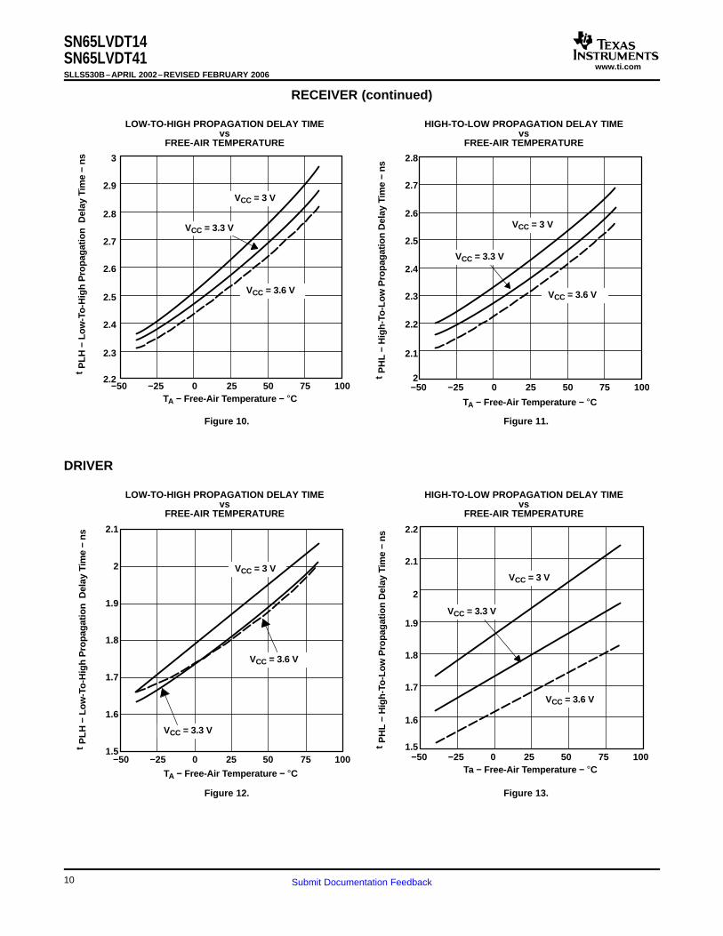
RECEIVER (continued)
LOW-TO-HIGH PROPAGATION DELAY TIME HIGH-TO-LOW PROPAGATION DELAY TIMEvs vs
FREE-AIR TEMPERATURE FREE-AIR TEMPERATURE
Figure 10. Figure 11.
LOW-TO-HIGH PROPAGATION DELAY TIME HIGH-TO-LOW PROPAGATION DELAY TIMEvs vs
FREE-AIR TEMPERATURE FREE-AIR TEMPERATURE
Figure 12. Figure 13.
10 Submit Documentation Feedback

www.ti.com
APPLICATION INFORMATION
EXTENDING THE MEMORY STICK INTERFACE USING LVDS SIGNALING OVER DIFFERENTIAL
1Y
1Z1D
1A
1B
5Y
5Z
1R
5D
2Y
2Z2D 2A
2B2R
3Y
3Z3D 3A
3B3R
4Y
4Z4D
4A
4B4R
5A
5B5R
SCLK
BS
DIR
SD1
SD2
CBT
SCLK
BS
SDIO
MemoryStick
CBT
SCLK
BS
SDIO
DIR
MemoryStickHost
Controller
SN65LVDT41 SN65LVDT14
SN65LVDT14SN65LVDT41
SLLS530B–APRIL 2002–REVISED FEBRUARY 2006
TRANSMISSION CABLES
Figure 14. System Level Block Diagram
The Memory Stick signaling interface operates in a LVDS, as specified by the TIA/EIA-644-A standard,master-slave architecture, with three active signal provides several benefits when compared tolines. The host (master) supplies a clock (SCLK) and alternative long-distance signaling technologies: lowbus-state (BS) signal to control the operation of the radiated emissions, high noise immunity, low powersystem. The SCLK and BS signals are unidirectional consumption, inexpensive interconnect cables.(simplex) from the host to the Memory Stick. The
This device pair provides the necessary LVDS driversserial data input-output (SDIO) signal is aand receivers specifically targeted at implementing abidirectional (half-duplex) signal used to communicateMemory Stick interconnect extension. It utilizesboth control and data information between the hostsimplex links for the SCLK and BS signals, and twoand the Memory Stick. The direction of data control issimplex links for the SDIO data. The half-duplexmanaged by the host through a combination of BSSDIO data is split into two simplex streams underline states and control information delivered to thecontrol of the host processor by means of theMemory Stick.direction (DIR) signal. The DIR signal is also carried
The basic Memory Stick interface is capable of from the host to the Memory Stick on a simplex LVDSoperating only over short distances due to the link.single-ended nature of the digital I/O signals. Such a
The switching of the SDIO signal flow direction in theconfiguration is entirely suitable for compact andsingle-ended interfaces is managed by electronicportable devices where there is little if any separationswitch devices, identified by the CBT symbol inbetween the host and the Memory Stick. InFigure 14. A suggested CBT device for thisapplications where a greater distance is neededapplication is the SN74CBTLV1G125 from Texasbetween the host controller and the Memory Stick, itInstruments Incorporated. These devices areis necessary to utilize a different signaling methodavailable in space saving SOT-23 or SC-70such as low voltage differential signaling, or LVDS.packages.
11Submit Documentation Feedback
PACKAGE OPTION ADDENDUM
www.ti.com 24-Apr-2015
Addendum-Page 1
PACKAGING INFORMATION
Orderable Device Status(1)
Package Type PackageDrawing
Pins PackageQty
Eco Plan(2)
Lead/Ball Finish(6)
MSL Peak Temp(3)
Op Temp (°C) Device Marking(4/5)
Samples
SN65LVDT14PW ACTIVE TSSOP PW 20 70 Green (RoHS& no Sb/Br)
CU NIPDAU Level-1-260C-UNLIM -40 to 85 LVDT14
SN65LVDT14PWG4 ACTIVE TSSOP PW 20 70 Green (RoHS& no Sb/Br)
CU NIPDAU Level-1-260C-UNLIM -40 to 85 LVDT14
SN65LVDT14PWR ACTIVE TSSOP PW 20 2000 Green (RoHS& no Sb/Br)
CU NIPDAU Level-1-260C-UNLIM -40 to 85 LVDT14
SN65LVDT14PWRG4 ACTIVE TSSOP PW 20 2000 Green (RoHS& no Sb/Br)
CU NIPDAU Level-1-260C-UNLIM -40 to 85 LVDT14
SN65LVDT41PW ACTIVE TSSOP PW 20 70 Green (RoHS& no Sb/Br)
CU NIPDAU Level-1-260C-UNLIM -40 to 85 LVDT41
SN65LVDT41PWG4 ACTIVE TSSOP PW 20 70 Green (RoHS& no Sb/Br)
CU NIPDAU Level-1-260C-UNLIM -40 to 85 LVDT41
SN65LVDT41PWR ACTIVE TSSOP PW 20 2000 Green (RoHS& no Sb/Br)
CU NIPDAU Level-1-260C-UNLIM -40 to 85 LVDT41
(1) The marketing status values are defined as follows:ACTIVE: Product device recommended for new designs.LIFEBUY: TI has announced that the device will be discontinued, and a lifetime-buy period is in effect.NRND: Not recommended for new designs. Device is in production to support existing customers, but TI does not recommend using this part in a new design.PREVIEW: Device has been announced but is not in production. Samples may or may not be available.OBSOLETE: TI has discontinued the production of the device.
(2) Eco Plan - The planned eco-friendly classification: Pb-Free (RoHS), Pb-Free (RoHS Exempt), or Green (RoHS & no Sb/Br) - please check http://www.ti.com/productcontent for the latest availabilityinformation and additional product content details.TBD: The Pb-Free/Green conversion plan has not been defined.Pb-Free (RoHS): TI's terms "Lead-Free" or "Pb-Free" mean semiconductor products that are compatible with the current RoHS requirements for all 6 substances, including the requirement thatlead not exceed 0.1% by weight in homogeneous materials. Where designed to be soldered at high temperatures, TI Pb-Free products are suitable for use in specified lead-free processes.Pb-Free (RoHS Exempt): This component has a RoHS exemption for either 1) lead-based flip-chip solder bumps used between the die and package, or 2) lead-based die adhesive used betweenthe die and leadframe. The component is otherwise considered Pb-Free (RoHS compatible) as defined above.Green (RoHS & no Sb/Br): TI defines "Green" to mean Pb-Free (RoHS compatible), and free of Bromine (Br) and Antimony (Sb) based flame retardants (Br or Sb do not exceed 0.1% by weightin homogeneous material)
(3) MSL, Peak Temp. - The Moisture Sensitivity Level rating according to the JEDEC industry standard classifications, and peak solder temperature.
(4) There may be additional marking, which relates to the logo, the lot trace code information, or the environmental category on the device.
PACKAGE OPTION ADDENDUM
www.ti.com 24-Apr-2015
Addendum-Page 2
(5) Multiple Device Markings will be inside parentheses. Only one Device Marking contained in parentheses and separated by a "~" will appear on a device. If a line is indented then it is a continuationof the previous line and the two combined represent the entire Device Marking for that device.
(6) Lead/Ball Finish - Orderable Devices may have multiple material finish options. Finish options are separated by a vertical ruled line. Lead/Ball Finish values may wrap to two lines if the finishvalue exceeds the maximum column width.
Important Information and Disclaimer:The information provided on this page represents TI's knowledge and belief as of the date that it is provided. TI bases its knowledge and belief on informationprovided by third parties, and makes no representation or warranty as to the accuracy of such information. Efforts are underway to better integrate information from third parties. TI has taken andcontinues to take reasonable steps to provide representative and accurate information but may not have conducted destructive testing or chemical analysis on incoming materials and chemicals.TI and TI suppliers consider certain information to be proprietary, and thus CAS numbers and other limited information may not be available for release.
In no event shall TI's liability arising out of such information exceed the total purchase price of the TI part(s) at issue in this document sold by TI to Customer on an annual basis.
OTHER QUALIFIED VERSIONS OF SN65LVDT14, SN65LVDT41 :
• Enhanced Product: SN65LVDT14-EP, SN65LVDT41-EP
NOTE: Qualified Version Definitions:
• Enhanced Product - Supports Defense, Aerospace and Medical Applications
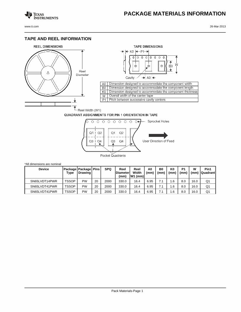
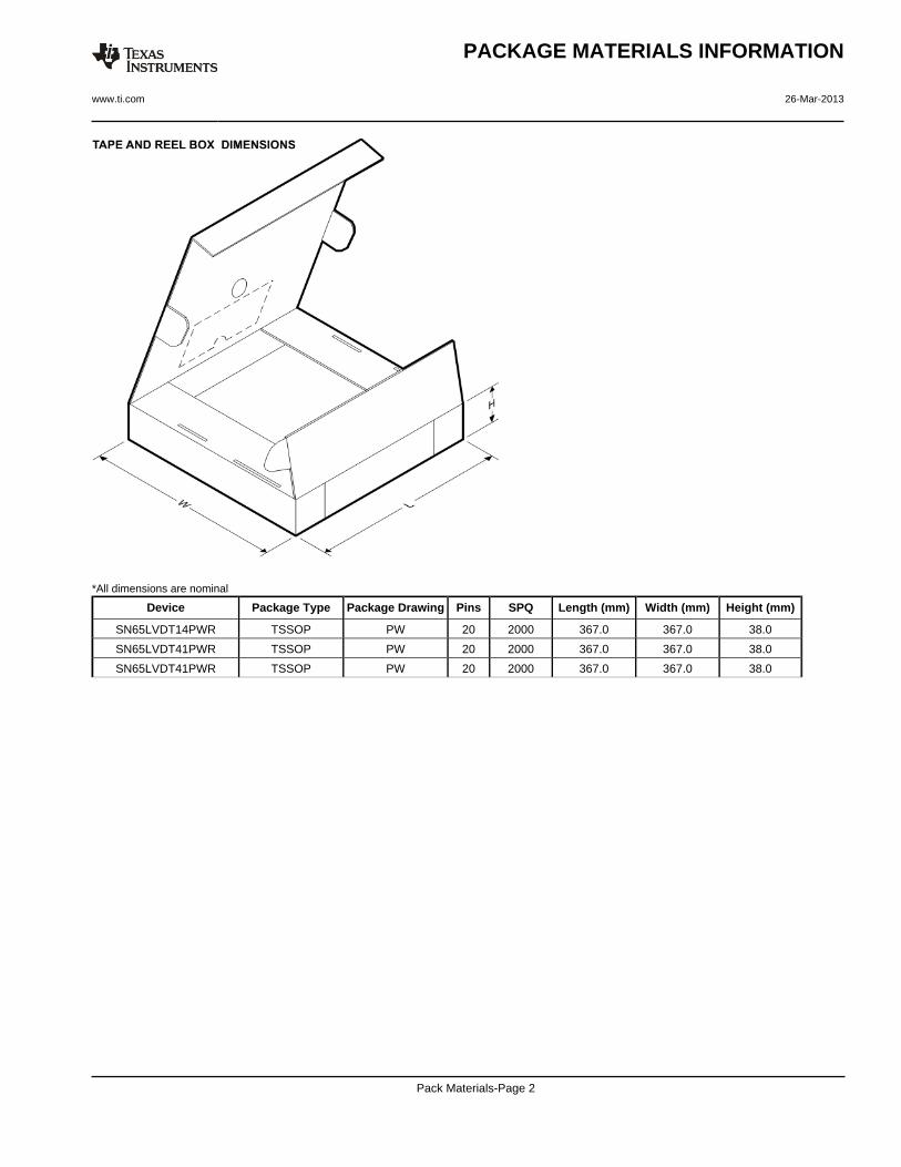
TAPE AND REEL INFORMATION
*All dimensions are nominal
Device PackageType
PackageDrawing
Pins SPQ ReelDiameter
(mm)
ReelWidth
W1 (mm)
A0(mm)
B0(mm)
K0(mm)
P1(mm)
W(mm)
Pin1Quadrant
SN65LVDT14PWR TSSOP PW 20 2000 330.0 16.4 6.95 7.1 1.6 8.0 16.0 Q1
SN65LVDT41PWR TSSOP PW 20 2000 330.0 16.4 6.95 7.1 1.6 8.0 16.0 Q1
SN65LVDT41PWR TSSOP PW 20 2000 330.0 16.4 6.95 7.1 1.6 8.0 16.0 Q1
PACKAGE MATERIALS INFORMATION
www.ti.com 26-Mar-2013
Pack Materials-Page 1
*All dimensions are nominal
Device Package Type Package Drawing Pins SPQ Length (mm) Width (mm) Height (mm)
SN65LVDT14PWR TSSOP PW 20 2000 367.0 367.0 38.0
SN65LVDT41PWR TSSOP PW 20 2000 367.0 367.0 38.0
SN65LVDT41PWR TSSOP PW 20 2000 367.0 367.0 38.0
PACKAGE MATERIALS INFORMATION
www.ti.com 26-Mar-2013
Pack Materials-Page 2

IMPORTANT NOTICE
Texas Instruments Incorporated and its subsidiaries (TI) reserve the right to make corrections, enhancements, improvements and otherchanges to its semiconductor products and services per JESD46, latest issue, and to discontinue any product or service per JESD48, latestissue. Buyers should obtain the latest relevant information before placing orders and should verify that such information is current andcomplete. All semiconductor products (also referred to herein as “components”) are sold subject to TI’s terms and conditions of salesupplied at the time of order acknowledgment.TI warrants performance of its components to the specifications applicable at the time of sale, in accordance with the warranty in TI’s termsand conditions of sale of semiconductor products. Testing and other quality control techniques are used to the extent TI deems necessaryto support this warranty. Except where mandated by applicable law, testing of all parameters of each component is not necessarilyperformed.TI assumes no liability for applications assistance or the design of Buyers’ products. Buyers are responsible for their products andapplications using TI components. To minimize the risks associated with Buyers’ products and applications, Buyers should provideadequate design and operating safeguards.TI does not warrant or represent that any license, either express or implied, is granted under any patent right, copyright, mask work right, orother intellectual property right relating to any combination, machine, or process in which TI components or services are used. Informationpublished by TI regarding third-party products or services does not constitute a license to use such products or services or a warranty orendorsement thereof. Use of such information may require a license from a third party under the patents or other intellectual property of thethird party, or a license from TI under the patents or other intellectual property of TI.Reproduction of significant portions of TI information in TI data books or data sheets is permissible only if reproduction is without alterationand is accompanied by all associated warranties, conditions, limitations, and notices. TI is not responsible or liable for such altereddocumentation. Information of third parties may be subject to additional restrictions.Resale of TI components or services with statements different from or beyond the parameters stated by TI for that component or servicevoids all express and any implied warranties for the associated TI component or service and is an unfair and deceptive business practice.TI is not responsible or liable for any such statements.Buyer acknowledges and agrees that it is solely responsible for compliance with all legal, regulatory and safety-related requirementsconcerning its products, and any use of TI components in its applications, notwithstanding any applications-related information or supportthat may be provided by TI. Buyer represents and agrees that it has all the necessary expertise to create and implement safeguards whichanticipate dangerous consequences of failures, monitor failures and their consequences, lessen the likelihood of failures that might causeharm and take appropriate remedial actions. Buyer will fully indemnify TI and its representatives against any damages arising out of the useof any TI components in safety-critical applications.In some cases, TI components may be promoted specifically to facilitate safety-related applications. With such components, TI’s goal is tohelp enable customers to design and create their own end-product solutions that meet applicable functional safety standards andrequirements. Nonetheless, such components are subject to these terms.No TI components are authorized for use in FDA Class III (or similar life-critical medical equipment) unless authorized officers of the partieshave executed a special agreement specifically governing such use.Only those TI components which TI has specifically designated as military grade or “enhanced plastic” are designed and intended for use inmilitary/aerospace applications or environments. Buyer acknowledges and agrees that any military or aerospace use of TI componentswhich have not been so designated is solely at the Buyer's risk, and that Buyer is solely responsible for compliance with all legal andregulatory requirements in connection with such use.TI has specifically designated certain components as meeting ISO/TS16949 requirements, mainly for automotive use. In any case of use ofnon-designated products, TI will not be responsible for any failure to meet ISO/TS16949.
Products ApplicationsAudio www.ti.com/audio Automotive and Transportation www.ti.com/automotiveAmplifiers amplifier.ti.com Communications and Telecom www.ti.com/communicationsData Converters dataconverter.ti.com Computers and Peripherals www.ti.com/computersDLP® Products www.dlp.com Consumer Electronics www.ti.com/consumer-appsDSP dsp.ti.com Energy and Lighting www.ti.com/energyClocks and Timers www.ti.com/clocks Industrial www.ti.com/industrialInterface interface.ti.com Medical www.ti.com/medicalLogic logic.ti.com Security www.ti.com/securityPower Mgmt power.ti.com Space, Avionics and Defense www.ti.com/space-avionics-defenseMicrocontrollers microcontroller.ti.com Video and Imaging www.ti.com/videoRFID www.ti-rfid.comOMAP Applications Processors www.ti.com/omap TI E2E Community e2e.ti.comWireless Connectivity www.ti.com/wirelessconnectivity
Mailing Address: Texas Instruments, Post Office Box 655303, Dallas, Texas 75265Copyright © 2015, Texas Instruments Incorporated