Embed Size (px)
Citation preview
Computer Systems
Han, Hwansoo
Memory Hierarchy

Random-Access Memory (RAM)
❖ Key features
▪ RAM is traditionally packaged as a chip.
▪ Basic storage unit is normally a cell (one bit per cell).
▪ Multiple RAM chips form a memory.
❖ RAM comes in two varieties:
▪ SRAM (Static RAM)
▪ DRAM (Dynamic RAM)

Random-Access Memory (RAM)
❖ Static RAM (SRAM)
▪ Each cell stores bit with a six-transistor circuit
▪ Retains value indefinitely, as long as it is kept powered
▪ Relatively insensitive to disturbances such as electrical noise
▪ Faster and more expensive than DRAM
❖ Dynamic RAM (DRAM)
▪ Each cell stores bit with a capacitor and transistor
▪ Value must be refreshed every 10-100ms
▪ Sensitive to disturbances
▪ Slower and cheaper than SRAM
Tran. Access Needper bit time refresh? Sensitive? Cost Applications
SRAM 6 1X No No 100x cache memories
DRAM 1 10X Yes Yes 1X Main memories, frame buffers
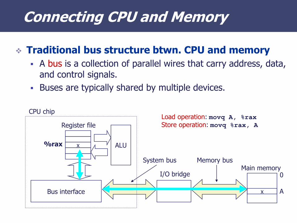
Connecting CPU and Memory
❖ Traditional bus structure btwn. CPU and memory
▪ A bus is a collection of parallel wires that carry address, data, and control signals.
▪ Buses are typically shared by multiple devices.
Bus interface
x ALU
Register file
CPU chip
System bus Memory bus
Load operation: movq A, %rax
Store operation: movq %rax, A
%rax
0
Ax
Main memoryI/O bridge

Conventional DRAM Organization
❖ d x w DRAM:
▪ dw total bits organized as d supercells of size w bits
cols
rows
0 1 2 3
0
1
2
3
internal row buffer
16 x 8 DRAM chip
addr
data
supercell
(2,1)
2 bits
/
8 bits
/
memory
controller(to CPU)

Reading DRAM Supercell (2,1)
▪ Step 1(a): Row access strobe (RAS) selects row 2.
▪ Step 1(b): Row 2 copied from DRAM array to row buffer.
cols
rows
RAS = 20 1 2 3
0
1
2
internal row buffer
16 x 8 DRAM chip
3
addr
data
2
/
8
/
memory
controller

Reading DRAM Supercell (2,1)
▪ Step 2(a): Column access strobe (CAS) selects column 1.
▪ Step 2(b): Supercell (2,1) copied from buffer to data lines, and eventually back to the CPU.
cols
rows
0 1 2 3
0
1
2
3
internal row buffer
16 x 8 DRAM chip
CAS = 1
addr
data
2
/
8
/
memory
controller
supercell
(2,1)
supercell
(2,1)
To CPU

Memory Modules (DIMMs)
: supercell (i,j)
64 MB
memory module
consisting of
eight 8Mx8 DRAMs
addr (row = i, col = j)
Memory
controller
DRAM 7
DRAM 0
031 78151623243263 394047485556
64-bit doubleword at main memory address A
bits
0-7
bits
8-15
bits
16-23
bits
24-31
bits
32-39
bits
40-47
bits
48-55
bits
56-63
64-bit doubleword
031 78151623243263 394047485556
64-bit doubleword at main memory address A

Nonvolatile Memories
❖ Nonvolatile memories retain value even if powered off.
▪ Generic name is read-only memory (ROM).
▪ Misleading because some ROMs can be read and modified.
❖ Types of ROMs
▪ Programmable ROM (PROM)
▪ Eraseable programming ROM (EPROM)
▪ Electrically eraseable PROM (EEPROM)
▪ Flash memory
❖ Firmware
▪ Program stored in a ROM
▪ Boot time code, BIOS (Basic Input/Output System)
▪ Graphics cards, disk controllers, etc.

What’s Inside A Disk Drive?
SpindleArm
Actuator
Platters
Electronics
(including a
processor
and memory!)SCSI
connector
[Image courtesy of Seagate Technology]

Disk Geometry
▪ Disks consist of platters, each with two surfaces.
▪ Each surface consists of concentric rings called tracks.
▪ Each track consists of sectors separated by gaps.
spindle
surfacetracks
track k
sectors
gaps

Multiple-platter View
❖ Aligned tracks form a cylinder
surface 0
surface 1surface 2
surface 3
surface 4
surface 5
cylinder k
spindle
platter 0
platter 1
platter 2
arm
read/write heads
move in unison
from cylinder to cylinder

Disk Operation
❖ Disk Operation (Single-platter view)
The disk
surface
spins at a
fixed
rotational rate
spindle
By moving radially, the
arm can position the
read/write head over any
track.
The read/write head
is attached to the end
of the arm and flies over
the disk surface on
a thin cushion of air.
sp
ind
le
spindle
sp
ind
le
spindle

Disk Capacity
❖ Capacity: maximum number of bits that can be stored
▪ Vendors express capacity in units of gigabytes (GB), where1 GB = 109 Bytes
❖ Capacity is determined by these technology factors:
▪ Recording density (bits/in): number of bits that can be squeezed into a 1 inch segment of a track
▪ Track density (tracks/in): number of tracks that can be squeezed into a 1 inch radial segment
▪ Areal density (bits/in2): product of recording and track density
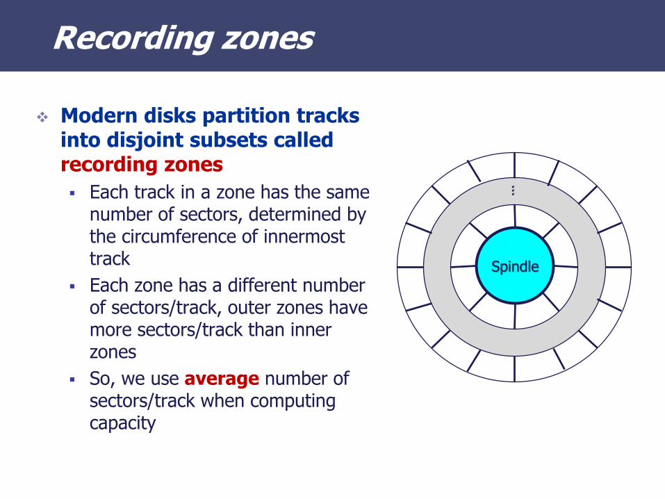
Recording zones
❖ Modern disks partition tracks into disjoint subsets called recording zones
▪ Each track in a zone has the same number of sectors, determined by the circumference of innermost track
▪ Each zone has a different number of sectors/track, outer zones have more sectors/track than inner zones
▪ So, we use average number of sectors/track when computing capacity
Spindle
…

Computing Disk Capacity
Capacity = (# bytes/sector) x (avg. # sectors/track) x
(# tracks/surface) x (# surfaces/platter) x
(# platters/disk)
Example:
▪ 512 bytes/sector
▪ 300 sectors/track (on average)
▪ 20,000 tracks/surface
▪ 2 surfaces/platter
▪ 5 platters/disk
Capacity = 512 x 300 x 20000 x 2 x 5
= 30,720,000,000
= 30.72 GB
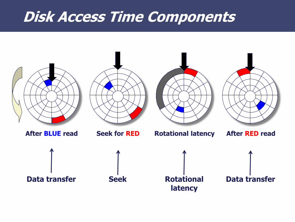
Disk Access Time Components
After BLUE read Seek for RED Rotational latency After RED read
Data transfer Seek Rotational latency
Data transfer

Disk Access Time
❖ Average time to access some target sector approximated by :
▪ Taccess = Tavg_seek + Tavg_rotation + Tavg_transfer
❖ Seek time
▪ Time to position heads over cylinder containing target sector.
▪ Typically 9ms
❖ Rotational latency
▪ Time waiting for first bit of target sector to pass under r/w head.
▪ ½ x 1/RPMs x 60 sec/1min
❖ Transfer time
▪ Time to read the bits in the target sector.
▪ 1/RPM x 1/(avg #sectors/track) x 60sec/1min
❖ Important points:
▪ Access time dominated by seek time.
▪ First bit in a sector is the most expensive, the rest are free.

Disk Access Time Example
❖ Given:▪ Rotational rate = 7,200 RPM
▪ Average seek time = 9 ms
▪ Avg # sectors/track = 400
❖ Derived:▪ Tavg rotation = 1/2 x (60 secs/7200 RPM) x 1000 ms/sec = 4 ms.
▪ Tavg transfer = 60/7200 RPM x 1/400 secs/track x 1000 ms/sec = 0.02 ms
▪ Taccess = 9 ms + 4 ms + 0.02 ms
❖ Important points:▪ Access time dominated by seek time and rotational latency.
▪ First bit in a sector is the most expensive, the rest are free.
▪ SRAM access time is about 4 ns/doubleword, DRAM about 60 ns▪ Disk is about 40,000 times slower than SRAM,
▪ 2,500 times slower then DRAM

Logical Disk Blocks
❖ Modern disks present a simple abstract view of the complex sector geometry:
▪ The set of available sectors is modeled as a sequence of block-sized logical blocks (0, 1, 2, …)
❖ Mapping between logical blocks and actual (physical) sectors
▪ Maintained by hardware/firmware device called disk controller.
▪ Converts requests for logical blocks into (surface, track, sector) triples
❖ Disk controller also performs some intelligent functions
▪ Buffering, caching, prefetching, scheduling, etc.

I/O Bus
main
memoryI/O
bridgebus interface
ALU
register file
CPU chip
system bus memory bus
disk
controller
graphics
adapter
USB
controller
mouse keyboard monitor
disk
I/O bus Expansion slots for
other devices such
as network adapters.

Reading a Disk Sector (1)
Mainmemory
ALU
Register file
CPU chip
Disk controller
Graphicsadapter
USBcontroller
mouse keyboard Monitor
Disk
I/O bus
Bus interface
CPU initiates a disk read by writing a command, logical block number, and destination memory address to a port(address) associated with disk controller.

Reading a Disk Sector (2)
Mainmemory
ALU
Register file
CPU chip
Disk controller
Graphicsadapter
USBcontroller
Mouse Keyboard Monitor
Disk
I/O bus
Bus interface
Disk controller reads the sector and performs a direct memory access (DMA) transfer into main memory.

Reading a Disk Sector (3)
Mainmemory
ALU
Register file
CPU chip
Disk controller
Graphicsadapter
USBcontroller
Mouse Keyboard Monitor
Disk
I/O bus
Bus interface
When the DMA transfer completes, the disk controller notifies the CPU with an interrupt (i.e., asserts a special “interrupt” pin on the CPU)

Solid State Disks (SSDs)
▪ Pages: 512B to 4KB, Blocks: 32 to 128 pages
▪ Data read/written in units of pages.
▪ Page can be written only after its block has been erased
▪ A block wears out after about 100,000 repeated writes.
Flash
translation layer
I/O bus
Page 0 Page 1 Page P-1…
Block 0
… Page 0 Page 1 Page P-1…
Block B-1
Flash memory
Solid State Disk (SSD)
Requests to read and write logical disk blocks

SSD Performance Characteristics
❖ Sequential access faster than random access
▪ Common theme in the memory hierarchy
❖ Random writes are somewhat slower
▪ Erasing a block takes a long time (~1 ms)
▪ Modifying a block page requires all other pages to be copied to new block
▪ In earlier SSDs, the read/write gap was much larger.
Sequential read tput 550 MB/s Sequential write tput 470 MB/sRandom read tput 365 MB/s Random write tput 303 MB/s
Avg seq read time 50 us Avg seq write time 60 us
[Source: Intel SSD 730 product specification]

SSD Tradeoffs vs. Rotating Disks
❖ Advantages ▪ No moving parts → faster, less power, more rugged
❖ Disadvantages
▪ Have the potential to wear out
▪ Mitigated by “wear leveling logic” in flash translation layer
▪ E.g. Intel SSD 730 guarantees 128 petabyte (128 x 1015 bytes) of writes before they wear out
▪ In 2017, about 7 times more expensive per byte
▪ 1TB: SSD (\400,000), HDD (\60,000)
❖ Applications
▪ MP3 players, smart phones, laptops
▪ Beginning to appear in desktops and servers

The CPU-Memory Gap
The gap between DRAM, disk, and CPU speeds.
0.0
0.1
1.0
10.0
100.0
1,000.0
10,000.0
100,000.0
1,000,000.0
10,000,000.0
100,000,000.0
1985 1990 1995 2000 2003 2005 2010 2015
Tim
e (
ns
)
Year
Disk seek time
SSD access time
DRAM access time
SRAM access time
CPU cycle time
Effective CPU cycle time
DRAM
CPU
SSD
Disk

Locality
❖ Principle of Locality: Programs tend to use data and instructions with addresses near or equal to those they have used recently
❖ Temporal locality:
▪ Recently referenced items are likely to be referenced again in the near future
❖ Spatial locality:
▪ Items with nearby addresses tend to be referenced close together in time

Locality Example
❖ Data references
▪ Reference array elements in succession (stride-1 reference pattern).
▪ Reference variable sum each iteration.
❖ Instruction references
▪ Reference instructions in sequence.
▪ Cycle through loop repeatedly.
sum = 0;
for (i = 0; i < n; i++)
sum += a[i];
return sum;
Spatial locality
Temporal locality
Spatial locality
Temporal locality

Qualitative Estimates of Locality
❖ Claim:
▪ Being able to look at code and get a qualitative sense of its locality is a key skill for a professional programmer.
❖ Question:
▪ Does this function have good locality with respect to array a?
int sum_array_rows(int a[M][N])
{
int i, j, sum = 0;
for (i = 0; i < M; i++)
for (j = 0; j < N; j++)
sum += a[i][j];
return sum;
}

Locality Example
❖ Question:
▪ Does this function have good locality with respect to array a?
int sum_array_cols(int a[M][N])
{
int i, j, sum = 0;
for (j = 0; j < N; j++)
for (i = 0; i < M; i++)
sum += a[i][j];
return sum;
}

Locality Example
❖ Question:
▪ Can you permute the loops so that the function scans the 3-d array a with a stride-1 reference pattern (and thus has
good spatial locality)?
int sum_array_3d(int a[M][N][N])
{
int i, j, k, sum = 0;
for (i = 0; i < M; i++)
for (j = 0; j < N; j++)
for (k = 0; k < N; k++)
sum += a[k][i][j];
return sum;
}
Observations on Code Locality
❖ Programmer can optimize for cache performance
▪ How data structures are organized
▪ How data are accessed
▪ Nested loop structure
▪ Blocking is a general technique
❖ All systems favor “cache friendly code”
▪ Getting absolute optimum performance is very platform specific
▪ Cache sizes, line sizes, associativities, etc.
▪ Can get most of the advantage with generic code
▪ Keep working set reasonably small (temporal locality)
▪ Use small strides (spatial locality)

Memory Hierarchies
❖ Some fundamental and enduring properties of hardware and software:
▪ Fast storage technologies cost more per byte and have less capacity.
▪ The gap between CPU and main memory speed is widening.
▪ Well-written programs tend to exhibit good locality.
❖ Memory hierarchy
▪ Efficient way of organizing memory and storage systems

Example Memory Hierarchy
Regs
L1 cache
(SRAM)
Main memory
(DRAM)
Local secondary storage
(local disks)
Larger,
slower,
and
cheaper
(per byte)
storage
devices
Remote secondary storage
(e.g., Web servers)
Local disks hold files
retrieved from disks
on remote servers
L2 cache
(SRAM)
L1 cache holds cache lines
retrieved from the L2 cache.
CPU registers hold words
retrieved from the L1 cache.
L2 cache holds cache lines
retrieved from L3 cache
L0:
L1:
L2:
L3:
L4:
L5:
Smaller,
faster,
and
costlier
(per byte)
storage
devices
L3 cache
(SRAM)L3 cache holds cache lines
retrieved from main memory.
L6:
Main memory holds
disk blocks retrieved
from local disks.

Caching
❖ Cache
▪ A smaller, faster storage device that acts as a staging area for a subset of the data in a larger, slower device
▪ Fundamental idea of a memory hierarchy:
▪ For each k, the faster, smaller device at level k serves as a cache for the larger, slower device at level k+1
❖ Why do memory hierarchies work?
▪ Programs tend to access the data at level k more often than the data at level k+1
▪ Thus, the storage at level k+1 can be slower, and thus larger and cheaper per bit
▪ Net effect: A large pool of memory that costs as much as the cheap storage near the bottom, but that serves data to programs at the rate of the fast storage near the top

General Cache Concepts: Hit
0 1 2 3
4 5 6 7
8 9 10 11
12 13 14 15
4 9 14 3Cache
Memory
Data in block b is neededRequest: 14
14Block b is in cache:
Hit!

General Cache Concepts: Miss
0 1 2 3
4 5 6 7
8 9 10 11
12 13 14 15
4 9 14 3Cache
Memory
Data in block b is neededRequest: 12
Block b is not in cache:Miss!
Block b is fetched frommemory
Request: 12
12
12
12
Block b is stored in cache• Placement policy:
determines where b goes•Replacement policy:
determines which blockgets evicted (victim)
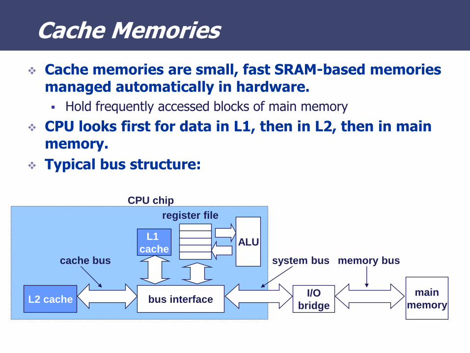
Cache Memories
❖ Cache memories are small, fast SRAM-based memories managed automatically in hardware.
▪ Hold frequently accessed blocks of main memory
❖ CPU looks first for data in L1, then in L2, then in main memory.
❖ Typical bus structure:
main
memoryI/O
bridgebus interfaceL2 cache
register file
ALU
CPU chip
cache bus system bus memory bus
L1
cache

General Org of a Cache Memory
▪ Cache is an array of sets.
▪ Each set contains one or more lines.
▪ Each line holds a block of data.
• • • B–110
• • • B–110
valid
valid
tag
tag
set 0:
B = 2b bytes
per cache block
E lines
per set
S = 2s sets
t tag bits
per line1 valid bit
per line
Cache size: C = B x E x S data bytes
• • •
• • • B–110
• • • B–110
valid
valid
tag
tag
set 1: • • •
• • • B–110
• • • B–110
valid
valid
tag
tag
set S-1: • • •
• • •

Addressing Caches
t bits s bits b bits
0m-1
<tag> <set index> <block offset>
Address A:
• • • B–110
• • • B–110
v
v
tag
tag
set 0: • • •
• • • B–110
• • • B–110
v
v
tag
tag
set 1: • • •
• • • B–110
• • • B–110
v
v
tag
tag
set S-1: • • •
• • •
The word at address A is in the cache ifthe tag bits in one of the <valid> lines in set <set index> match <tag>.
The word contents begin at offset <block offset> bytes from the beginning of the block.

Direct-Mapped Cache
❖ Simplest kind of cache
❖ Characterized by exactly one line per set.
valid
valid
valid
tag
tag
tag
• • •
set 0:
set 1:
set S-1:
E=1 lines per setcache block
cache block
cache block

Accessing Direct-Mapped Caches
❖ Set selection
▪ Use the set index bits to determine the set of interest.
valid
valid
valid
tag
tag
tag
• • •
set 0:
set 1:
set S-1:t bits s bits
0 0 0 0 1
0m-1
b bits
tag set index block offset
selected set
cache block
cache block
cache block

Accessing Direct-Mapped Caches
❖ Line matching and word selection
▪ Line matching: Find a valid line in the selected set with a matching tag
▪ Word selection: Then extract the word
1
t bits s bits
100i0110
0m-1
b bits
tag set index block offset
selected set (i):
(3) If (1) and (2), then cache hit,
and block offset selects
starting byte.
=1? (1) The valid bit must be set
= ?(2) The tag bits in the cache
line must match thetag bits in the address
0110 w3w0 w1 w2
30 1 2 74 5 6
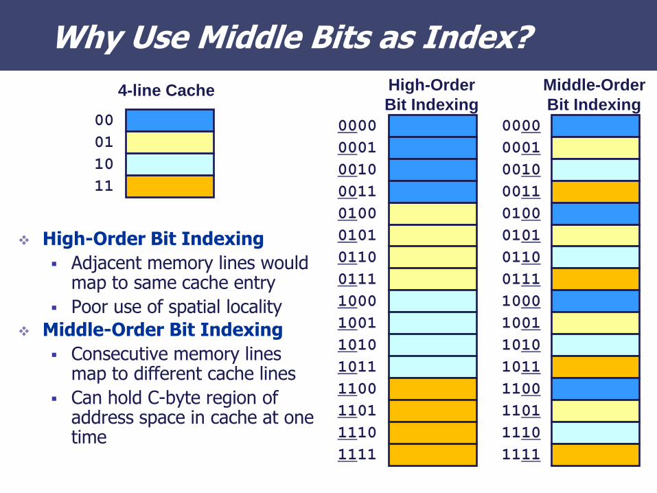
Why Use Middle Bits as Index?
❖ High-Order Bit Indexing
▪ Adjacent memory lines would map to same cache entry
▪ Poor use of spatial locality
❖ Middle-Order Bit Indexing
▪ Consecutive memory lines map to different cache lines
▪ Can hold C-byte region of address space in cache at one time
4-line Cache High-Order
Bit Indexing
Middle-Order
Bit Indexing00
01
10
11
0000
0001
0010
0011
0100
0101
0110
0111
1000
1001
1010
1011
1100
1101
1110
1111
0000
0001
0010
0011
0100
0101
0110
0111
1000
1001
1010
1011
1100
1101
1110
1111

Set Associative Caches
❖ Characterized by more than one line per set
valid tagset 0: E=2 lines per set
set 1:
set S-1:
• • •
cache block
valid tag cache block
valid tag cache block
valid tag cache block
valid tag cache block
valid tag cache block

Accessing Set Associative Caches
❖ Set selection
▪ identical to direct-mapped cache
valid
valid
tag
tag
set 0:
valid
valid
tag
tag
set 1:
valid
valid
tag
tagset S-1:
• • •
t bits s bits
0 0 0 0 1
0m-1
b bits
tag set index block offset
Selected set
cache block
cache block
cache block
cache block
cache block
cache block
Accessing Set Associative Caches
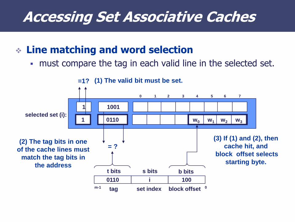
❖ Line matching and word selection
▪ must compare the tag in each valid line in the selected set.
1 0110 w3w0 w1 w2
1 1001
t bits s bits
100i0110
0m-1
b bits
tag set index block offset
selected set (i):
=1? (1) The valid bit must be set.
= ?(2) The tag bits in one
of the cache lines must
match the tag bits in
the address
(3) If (1) and (2), then
cache hit, and
block offset selects
starting byte.
30 1 2 74 5 6
Cache Performance Metrics
❖ Miss Rate
▪ Fraction of memory references not found in cache (misses/references)
▪ Typical numbers:
▪ 3-10% for L1
▪ can be quite small (e.g., < 1%) for L2, depending on size, etc.
❖ Hit Time
▪ Time to deliver a line in the cache to the processor (includes time to determine whether the line is in the cache)
▪ Typical numbers:
▪ 1 clock cycle for L1
▪ 3-8 clock cycles for L2
❖ Miss Penalty
▪ Additional time required because of a miss
▪ Typically 25-100 cycles for main memory

Examples of Caching
Hardware MMU
0On-Chip TLBAddress translationsTLB
Web browser10,000,000Local diskWeb pagesBrowser cache
Web cache
Network buffer cache
Buffer cache
Virtual Memory
L2 cache
L1 cache
Registers
Cache Type
Web pages
Parts of files
Parts of files
4-KB pages
64-byte blocks
64-byte blocks
4-8 bytes words
What is Cached?
Web proxy server
1,000,000,000Remote server disks
OS100Main memory
Hardware4On-Chip L1
Hardware10On-Chip L2
NFS client10,000,000Local disk
Hardware + OS100Main memory
Compiler0CPU core
Managed ByLatency (cycles)Where is it Cached?
Disk cache Disk sectors Disk controller 100,000 Disk firmware

Summary
❖ Devices with various access times & capacities
▪ SRAM
▪ DRAM
▪ Disk (SSD/HDD)
❖ Hierarchy works
▪ Need to hold large data
▪ Need to access data fast
❖ Caching principle for hierarchy
▪ Temporal locality
▪ Spatial locality