Embed Size (px)
Citation preview
1
Spring 2002 EECS150 - Lec19-memory Page 1
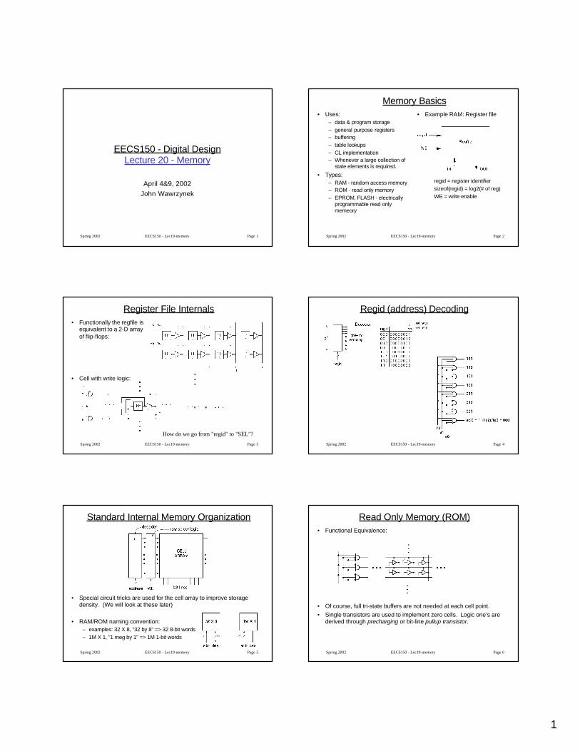
EECS150 - Digital DesignLecture 20 - Memory
April 4&9, 2002
John Wawrzynek
Spring 2002 EECS150 - Lec19-memory Page 2
Memory Basics• Uses:
– data & program storage– general purpose registers– buffering– table lookups– CL implementation– Whenever a large collection of
state elements is required.
• Types:– RAM - random access memory– ROM - read only memory– EPROM, FLASH - electrically
programmable read onlymemeory
• Example RAM: Register file
regid = register identifiersizeof(regid) = log2(# of reg)WE = write enable
Spring 2002 EECS150 - Lec19-memory Page 3
Register File Internals• Functionally the regfile is
equivalent to a 2-D arrayof flip-flops:
• Cell with write logic:
How do we go from "regid" to "SEL"?
Spring 2002 EECS150 - Lec19-memory Page 4
Regid (address) Decoding
Spring 2002 EECS150 - Lec19-memory Page 5
Standard Internal Memory Organization
• Special circuit tricks are used for the cell array to improve storagedensity. (We will look at these later)
• RAM/ROM naming convention:– examples: 32 X 8, "32 by 8" => 32 8-bit words– 1M X 1, "1 meg by 1" => 1M 1-bit words
Spring 2002 EECS150 - Lec19-memory Page 6
Read Only Memory (ROM)• Functional Equivalence:
• Of course, full tri-state buffers are not needed at each cell point.
• Single transistors are used to implement zero cells. Logic one’s arederived through precharging or bit-line pullup transistor.
2
Spring 2002 EECS150 - Lec19-memory Page 7
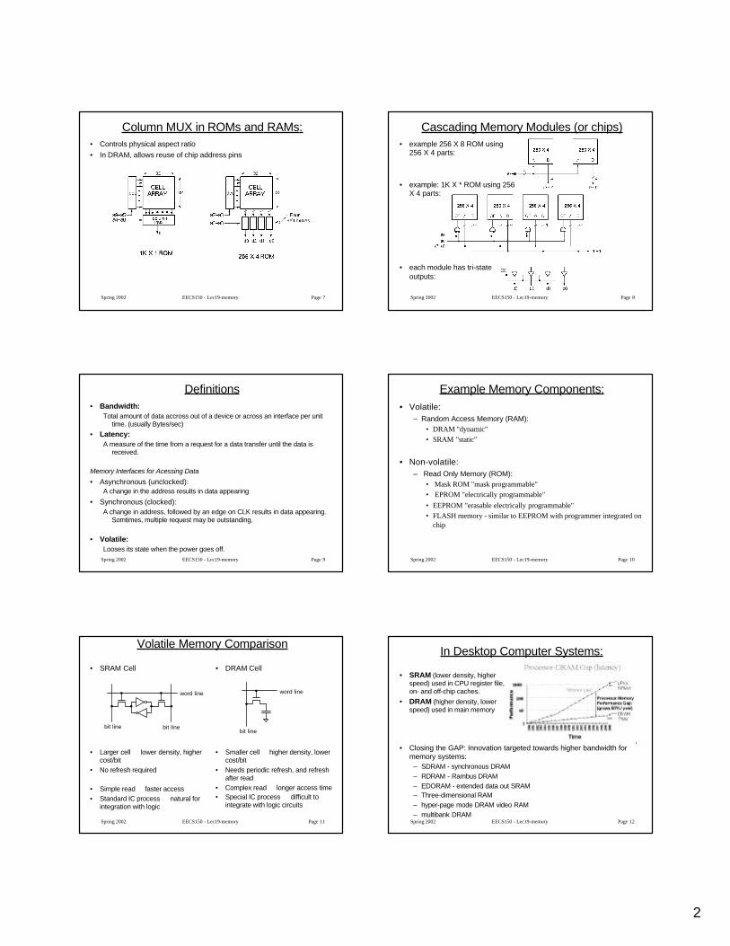
Column MUX in ROMs and RAMs:• Controls physical aspect ratio
• In DRAM, allows reuse of chip address pins
Spring 2002 EECS150 - Lec19-memory Page 8
Cascading Memory Modules (or chips)• example 256 X 8 ROM using
256 X 4 parts:
• example: 1K X * ROM using 256X 4 parts:
• each module has tri-stateoutputs:
Spring 2002 EECS150 - Lec19-memory Page 9
Definitions• Bandwidth:
Total amount of data accross out of a device or across an interface per unittime. (usually Bytes/sec)
• Latency:A measure of the time from a request for a data transfer until the data is
received.
Memory Interfaces for Acessing Data
• Asynchronous (unclocked):A change in the address results in data appearing
• Synchronous (clocked):A change in address, followed by an edge on CLK results in data appearing.
Somtimes, multiple request may be outstanding.
• Volatile:Looses its state when the power goes off.
Spring 2002 EECS150 - Lec19-memory Page 10
Example Memory Components:• Volatile:
– Random Access Memory (RAM):• DRAM "dynamic"• SRAM "static"
• Non-volatile:– Read Only Memory (ROM):
• Mask ROM "mask programmable"• EPROM "electrically programmable"
• EEPROM "erasable electrically programmable"• FLASH memory - similar to EEPROM with programmer integrated on
chip
Spring 2002 EECS150 - Lec19-memory Page 11
Volatile Memory Comparison
• SRAM Cell
• Larger cell ⇒ lower density, highercost/bit
• No refresh required
• Simple read ⇒ faster access• Standard IC process ⇒ natural for
integration with logic
• DRAM Cell
• Smaller cell ⇒ higher density, lowercost/bit
• Needs periodic refresh, and refreshafter read
• Complex read ⇒ longer access time• Special IC process ⇒ difficult to
integrate with logic circuits
word line
bit line bit line
word line
bit line
Spring 2002 EECS150 - Lec19-memory Page 12
In Desktop Computer Systems:
• SRAM (lower density, higherspeed) used in CPU register file,on- and off-chip caches.
• DRAM (higher density, lowerspeed) used in main memory
• Closing the GAP: Innovation targeted towards higher bandwidth formemory systems:
– SDRAM - synchronous DRAM– RDRAM - Rambus DRAM– EDORAM - extended data out SRAM – Three-dimensional RAM– hyper-page mode DRAM video RAM– multibank DRAM
3
Spring 2002 EECS150 - Lec19-memory Page 13
Important DRAM Examples:• EDO - extended data out (similar to fast-page mode)
– RAS cycle fetched rows of data from cell array blocks (long access time,around 100ns)
– Subsequent CAS cycles quickly access data from row buffers if within anaddress page (page is around 256 Bytes)
• SDRAM - synchronous DRAM– clocked interface– uses dual banks internally. Start access in one back then next, then
receive data from first then second.
• DDR - Double data rate SDRAM– Uses both rising (positive edge) and falling (negative) edge of clock for
data transfer. (typical 100MHz clock with 200 MHz transfer).
• RDRAM - Rambus DRAM– Entire data blocks are access and transferred out on a highspeed bus-like
interface (500 MB/s, 1.6 GB/s)– Tricky system level design. More expensive memory chips.
Spring 2002 EECS150 - Lec19-memory Page 14
Non-volatile Memory
• Mask ROM– Used with logic circuits for tables etc.– Contents fixed at IC fab time (truly write once!)
• EPROM (erasable programmable) & FLASH
– requires special IC process(floating gate technology)
– writing is slower than RAM. EPROM uses special programming system toprovide special voltages and timing.
– reading can be made fairly fast.– rewriting is very slow.
• erasure is first required , EPROM - UV light exposure
Used to hold fixed code (ex. BIOS), tables of data (ex. FSM next state/outputlogic), slowly changing values (date/time on computer)
Spring 2002 EECS150 - Lec19-memory Page 15
FLASH Memory• Electrically erasable
• In system programmability and erasability (no special system orvoltages needed)
• On-chip circuitry (FSM) to control erasure and programming (writing)
• Erasure happens in variable sized "sectors" in a flash (16K - 64KBytes)
See: http://developer.intel.com/design/flash/for product descriptions, etc.
Spring 2002 EECS150 - Lec19-memory Page 16
Relationship between Memory and CL• Memory blocks can be (and
often are) used to implementcombinational logic functions:
• Examples:– LUTs in FPGAs– 1Mbit x 8 EPROM can
implement 8 independentfunctions each of log2(1M)=20inputs.
• The decoder part of a memoryblock can be considered a“minterm generator”.
• The cell array part of a memoryblock can be considered an ORfunction over a subset of rows.
• The combination gives us a wayto implement logic functionsdirectly in sum of products form.
• Several variations on this themeexist in a set of devices calledProgrammable logic devices(PLDs)
Spring 2002 EECS150 - Lec19-memory Page 17
A ROM as AND/OR Logic Device
Spring 2002 EECS150 - Lec19-memory Page 18
PLD Summary
4
Spring 2002 EECS150 - Lec19-memory Page 19
PLA Example
Spring 2002 EECS150 - Lec19-memory Page 20
PAL Example
Spring 2002 EECS150 - Lec19-memory Page 21
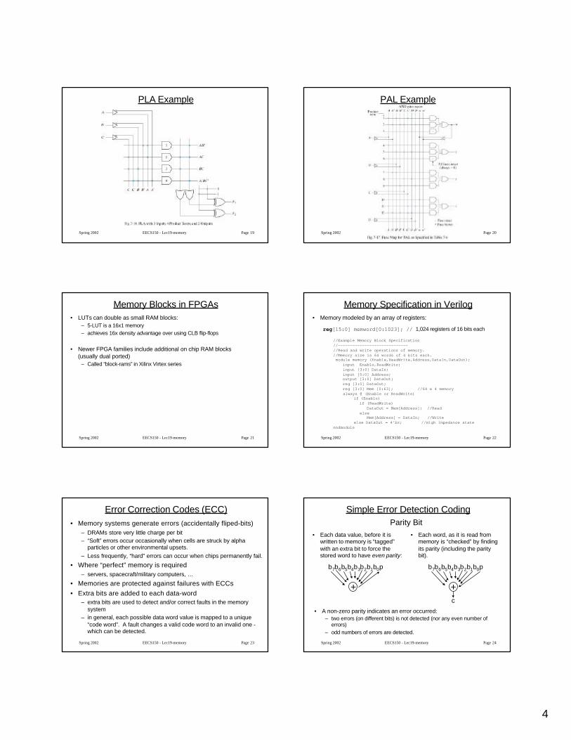
Memory Blocks in FPGAs• LUTs can double as small RAM blocks:
– 5-LUT is a 16x1 memory– achieves 16x density advantage over using CLB flip-flops
• Newer FPGA families include additional on chip RAM blocks(usually dual ported)
– Called “block-rams” in Xilinx Virtex series
Spring 2002 EECS150 - Lec19-memory Page 22
Memory Specification in Verilog• Memory modeled by an array of registers:
reg[15:0] memword[0:1023]; // 1,024 registers of 16 bits each
//Example Memory Block Specification//----------------------------- //Read and write operations of memory.//Memory size is 64 words of 4 bits each. module memory (Enable,ReadWrite,Address,DataIn,DataOut); input Enable,ReadWrite; input [3:0] DataIn; input [5:0] Address; output [3:0] DataOut; reg [3:0] DataOut; reg [3:0] Mem [0:63]; //64 x 4 memory always @ (Enable or ReadWrite)
if (Enable) if (ReadWrite) DataOut = Mem[Address]; //Read else Mem[Address] = DataIn; //Write
else DataOut = 4'bz; //High impedance stateendmodule
Spring 2002 EECS150 - Lec19-memory Page 23
Error Correction Codes (ECC)• Memory systems generate errors (accidentally fliped-bits)
– DRAMs store very little charge per bit– “Soft” errors occur occasionally when cells are struck by alpha
particles or other environmental upsets.
– Less frequently, “hard” errors can occur when chips permanently fail.
• Where “perfect” memory is required– servers, spacecraft/military computers, …
• Memories are protected against failures with ECCs
• Extra bits are added to each data-word– extra bits are used to detect and/or correct faults in the memory
system– in general, each possible data word value is mapped to a unique
“code word”. A fault changes a valid code word to an invalid one -which can be detected.
Spring 2002 EECS150 - Lec19-memory Page 24
Simple Error Detection Coding
• Each data value, before it iswritten to memory is “tagged”with an extra bit to force thestored word to have even parity:
• Each word, as it is read frommemory is “checked” by findingits parity (including the paritybit).
Parity Bit
b7b6b5b4b3b2b1b0p
+
b7b6b5b4b3b2b1b0p
+c
• A non-zero parity indicates an error occurred:– two errors (on different bits) is not detected (nor any even number of
errors)– odd numbers of errors are detected.
5
Spring 2002 EECS150 - Lec19-memory Page 25
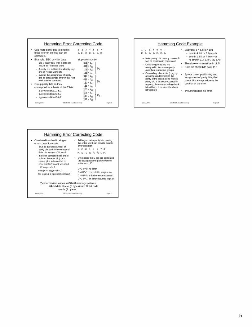
Hamming Error Correcting Code• Use more parity bits to pinpoint
bit(s) in error, so they can becorrected.
• Example: SEC on 4-bit data– use 3 parity bits, with 4-data bits
results in 7-bit code word– 3 parity bits sufficient to identify any
one of 7 code word bits– overlap the assignment of parity
bits so that a single error in the 7-bitwork can be corrected
• Group parity bits so theycorrespond to subsets of the 7 bits:
– p1 protects bits 1,3,5,7– p2 protects bits 2,3,6,7– p3 protects bits 4,5,6,7
1 2 3 4 5 6 7p1 p2 d1 p3 d2 d3 d4
Bit position number001 = 110
011 = 310
101 = 510
111 = 710
010 = 210
011 = 310
110 = 610
111 = 710
100 = 410
101 = 510
110 = 610
111 = 710
p1
p2
p3
Spring 2002 EECS150 - Lec19-memory Page 26
Hamming Code Example• Example: c = c1c2c3= 101
– error in 4,5,6, or 7 (by c3=1)– error in 1,3,5, or 7 (by c1=1)– no error in 2, 3, 6, or 7 (by c2=0)
• Therefore error must be in bit 5.• Note the check bits point to 5
• By our clever positioning andassignment of parity bits, thecheck bits always address theposition of the error!
• c=000 indicates no error
1 2 3 4 5 6 7p1 p2 d1 p3 d2 d3 d4
– Note: parity bits occupy power-of-two bit positions in code-word.
– On writing parity bits areassigned to force even parityover their respective groups.
– On reading, check bits (c1,c2,c3)are generated by finding theparity of the group along with itsparity bit. If an error occurred ina group, the corresponding checkbit will be 1, if no error the checkbit will be 0.
Spring 2002 EECS150 - Lec19-memory Page 27
Hamming Error Correcting Code• Overhead involved in single
error correction code:– let p be the total number of
parity bits and d the number ofdata bits in a p + d bit word.
– If p error correction bits are topoint to the error bit (p + dcases) plus indicate that noerror exists (1 case), we need:
2p >= p + d + 1,thus p >= log(p + d + 1)for large d, p approaches log(d)
• Adding on extra parity bit coveringthe entire word can provide doubleerror detection
1 2 3 4 5 6 7 8 p1 p2 d1 p3 d2 d3 d4 p4
• On reading the C bits are computed(as usual) plus the parity over theentire word, P:
C=0 P=0, no errorC!=0 P=1, correctable single errorC!=0 P=0, a double error occurredC=0 P=1, an error occurred in p4 bit
Typical modern codes in DRAM memory systems:64-bit data blocks (8 bytes) with 72-bit code
words (9 bytes).