Embed Size (px)
Citation preview
©2015 Micron Technology, Inc. All rights reserved. Information, products, and/or specifications are subject to
change without notice. All information is provided on an “AS IS” basis without warranties of any kind.
Statements regarding products, including regarding their features, availability, functionality, or compatibility,
are provided for informational purposes only and do not modify the warranty, if any, applicable to any
product. Drawings may not be to scale. Micron, the Micron logo, and all other Micron trademarks are the
property of Micron Technology, Inc. All other trademarks are the property of their respective owners.
Title Slide
Primary design
for the first slide
in the deck.
Memory as We
Approach a New Horizon
Hot Chips 2016 Memory Tutorial
J. Thomas Pawlowski, Chief Technologist, Fellow
©2016 Micron Technology, Inc. All rights reserved. Information, products, and/or specifications are subject to
change without notice. All information is provided on an “AS IS” basis without warranties of any kind.
Statements regarding products, including regarding their features, availability, functionality, or compatibility,
are provided for informational purposes only and do not modify the warranty, if any, applicable to any
product. Drawings may not be to scale. Micron, the Micron logo, and all other Micron trademarks are the
property of Micron Technology, Inc. All other trademarks are the property of their respective owners.
© 2016 Micron Technology, Inc.
Title and Content
The primary layout
used for standard
slides. The
placeholder can be
used to create text,
tables, or charts.
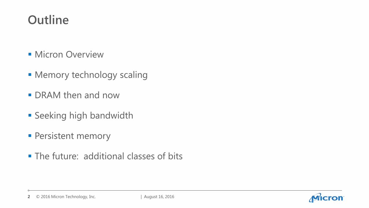
Outline
Micron Overview
Memory technology scaling
DRAM then and now
Seeking high bandwidth
Persistent memory
The future: additional classes of bits
| August 16, 2016 2
© 2016 Micron Technology, Inc.
Title and Content
The primary layout
used for standard
slides. The
placeholder can be
used to create text,
tables, or charts.
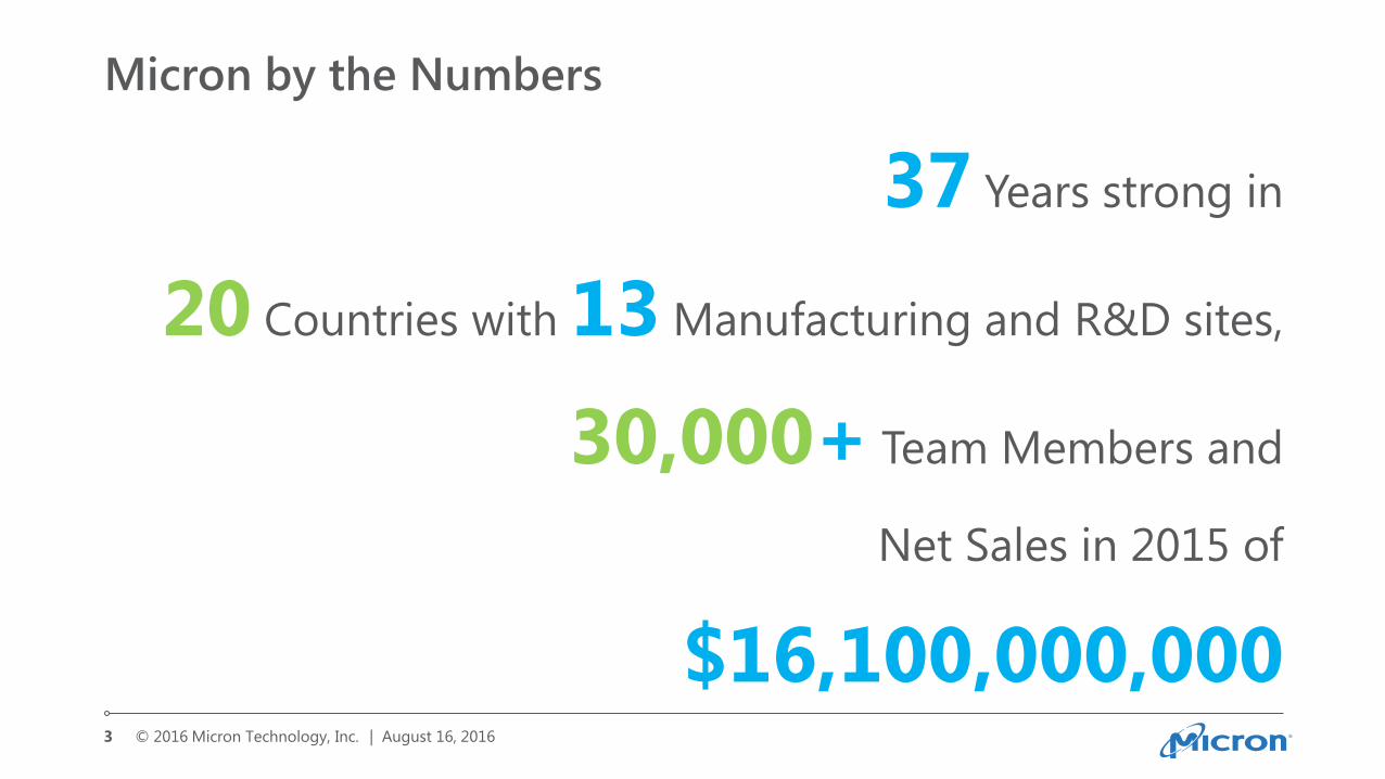
Micron by the Numbers
37 Years strong in
20 Countries with 13 Manufacturing and R&D sites,
30,000+ Team Members and
Net Sales in 2015 of
$16,100,000,000 3 | August 16, 2016
© 2016 Micron Technology, Inc.
Title/Subtitle
and Content
Identical to main
layout but includes
the addition of a
subtitle directly
below the title.
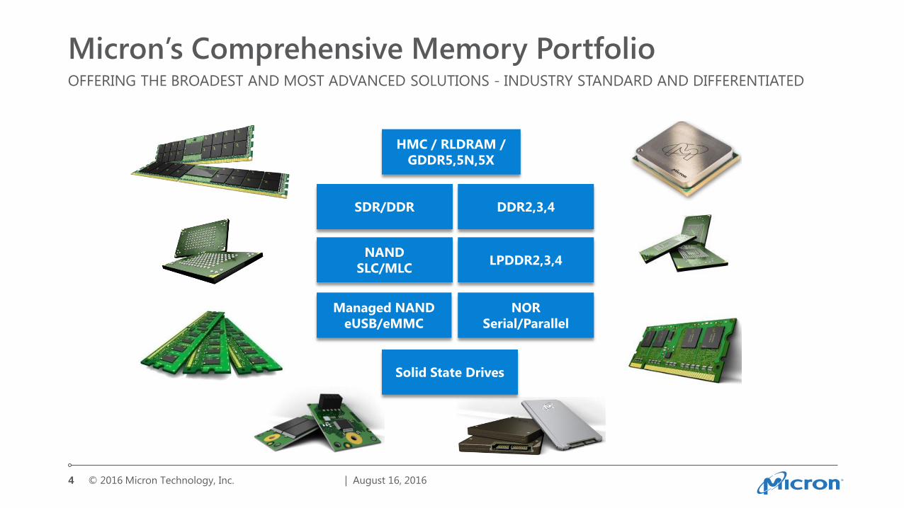
Micron’s Comprehensive Memory Portfolio OFFERING THE BROADEST AND MOST ADVANCED SOLUTIONS - INDUSTRY STANDARD AND DIFFERENTIATED
| August 16, 2016 4
SDR/DDR DDR2,3,4
NAND
SLC/MLC
NOR
Serial/Parallel
HMC / RLDRAM /
GDDR5,5N,5X
Managed NAND
eUSB/eMMC
Solid State Drives
LPDDR2,3,4

Full Photo
with Left Text
For integrating text
and photos.
| August 16, 2016
5
IoT 50 billion connected
devices in 2020
Enterprise OLTP systems with low-
latency in-memory compute
Cloud/Big Data 44 zettabytes
of stored data
Mobile/Client 38 exabytes of traffic
per year, driven by video / photos / apps
Networking 60% more traffic
per year with 30%
less energy
Unprecedented Data Growth Driving System Evolution
Sources: Gartner, Cisco Visual Networking Index, European Commission, HP.com
Automobile Customer-ready
autonomous vehicles by 2020
© 2016 Micron Technology, Inc.
Title and Content
The primary layout
used for standard
slides. The
placeholder can be
used to create text,
tables, or charts.
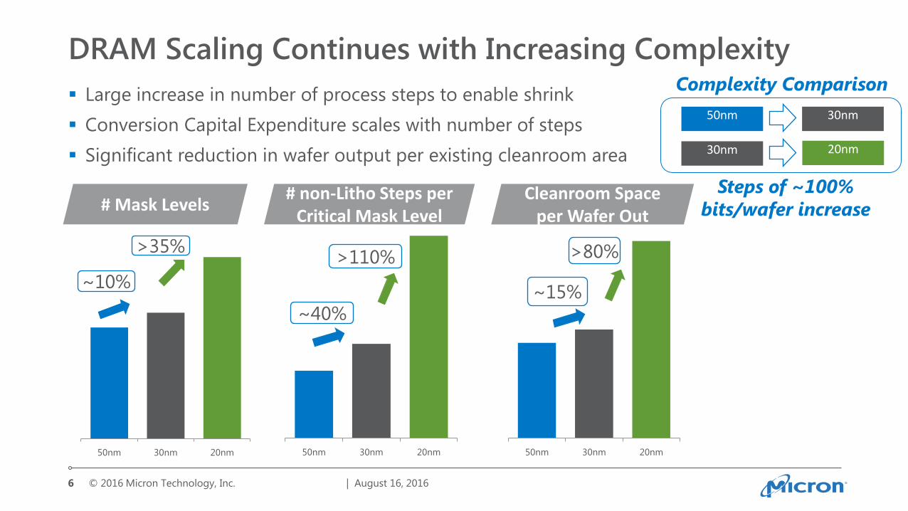
DRAM Scaling Continues with Increasing Complexity
Large increase in number of process steps to enable shrink
Conversion Capital Expenditure scales with number of steps
Significant reduction in wafer output per existing cleanroom area
| August 16, 2016 6
50nm 30nm 20nm
# Mask Levels Cleanroom Space
per Wafer Out
~10%
>35%
~15%
>80%
50nm 30nm 20nm
# non-Litho Steps per Critical Mask Level
~40%
>110%
Steps of ~100%
bits/wafer increase
50nm
30nm
30nm
20nm
50nm 30nm 20nm
Complexity Comparison
© 2016 Micron Technology, Inc.
Title and Content
The primary layout
used for standard
slides. The
placeholder can be
used to create text,
tables, or charts.
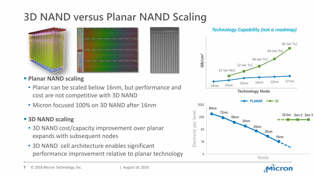
3D NAND versus Planar NAND Scaling
Planar NAND scaling
• Planar can be scaled below 16nm, but performance and cost are not competitive with 3D NAND
• Micron focused 100% on 3D NAND after 16nm
3D NAND scaling
• 3D NAND cost/capacity improvement over planar expands with subsequent nodes
• 3D NAND cell architecture enables significant performance improvement relative to planar technology
| August 16, 2016 7
Node
90nm
Ele
ctro
ns
per
level
4
16
64
256
1024
72nm
50nm 34nm
25nm
20nm
16nm
32-tier Gen 2 Gen 3
PLANAR 3D
34nm 25nm 20nm 16nm 1Znm 1Z'nm
32-tier MLC
32-tier TLC
48-tier TLC
64-tier TLC
96-tier TLC
GB
/cm
2
Technology Node
Technology Capability (not a roadmap)
© 2016 Micron Technology, Inc.
Title and Content
The primary layout
used for standard
slides. The
placeholder can be
used to create text,
tables, or charts.
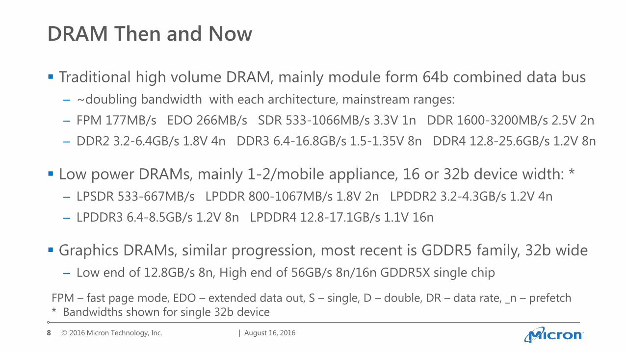
DRAM Then and Now
Traditional high volume DRAM, mainly module form 64b combined data bus
– ~doubling bandwidth with each architecture, mainstream ranges:
– FPM 177MB/s EDO 266MB/s SDR 533-1066MB/s 3.3V 1n DDR 1600-3200MB/s 2.5V 2n
– DDR2 3.2-6.4GB/s 1.8V 4n DDR3 6.4-16.8GB/s 1.5-1.35V 8n DDR4 12.8-25.6GB/s 1.2V 8n
Low power DRAMs, mainly 1-2/mobile appliance, 16 or 32b device width: *
– LPSDR 533-667MB/s LPDDR 800-1067MB/s 1.8V 2n LPDDR2 3.2-4.3GB/s 1.2V 4n
– LPDDR3 6.4-8.5GB/s 1.2V 8n LPDDR4 12.8-17.1GB/s 1.1V 16n
Graphics DRAMs, similar progression, most recent is GDDR5 family, 32b wide
– Low end of 12.8GB/s 8n, High end of 56GB/s 8n/16n GDDR5X single chip
| August 16, 2016 8
FPM – fast page mode, EDO – extended data out, S – single, D – double, DR – data rate, _n – prefetch
* Bandwidths shown for single 32b device
© 2016 Micron Technology, Inc.
Title and Content
The primary layout
used for standard
slides. The
placeholder can be
used to create text,
tables, or charts.
| August 16, 2016 9
High Performance DRAM Comparison Type DDR3/DDR3L DDR4 LPDDR4 GDDR5N RL3
Die Density Up to 16Gb Up to 16Gb Up to 32Gb Up to 8Gb Up to 1Gb
Prefetch Size 8n 8n 16n 8n 2n
Core Voltage (Vdd) 1.5V/1.35V 1.2V 1.10 1.35V 1.35V
I/O Voltage Same as VDD Same as VDD Same as VDD Same as VDD 1.2V
Max Clock Frequency Max Data Rate
1066MHz
DDR2100
1600MHz
DDR3200
2133MHz
DDR4267
1250MHz
DDR5000
1200MHz
DDR2400
Burst Length BC4, 8 BC4, 8 16, 32 8 2,4,8
Device Width (I/O) x4, x8, x16 x4, x8, x16 2Ch x16 x16,x32 x18, x36
Internal Banks 8 16 (x4/x8), 8 (x16) 8/Ch 16 16
Bank Groups N/A 4 (x4/x8), 2 (x16) N/A 4 N/A
On Die Temperature
Sensor Optional/RS Yes Yes Yes N/A
Row Cycle Time (tRC) 43 to 52ns 45 to 50ns 60 to 63ns 40 to 44ns 6.67 to 8ns
Bank Address Delays
(tRRD/tFAW)*
5.0–10ns/
25–40ns
2.5-7.5ns/
10-35ns
10ns/
40ns
4ns/
16ns NA
Bus Turn Delay (tWTR)* 7.5ns 2.5 to 11.25ns 10ns 5.1 to 5.6ns 0.83 to 1.07ns
Refresh Penalty (tRFC) 110-350ns 160-350ns 130-180 (all bank)
60-90 (per bank) 65-110ns N/A
*Minimum associated clock cycles may also apply
Networking Inspired Mobile Inspired Server Inspired
© 2016 Micron Technology, Inc.
Title and Content
The primary layout
used for standard
slides. The
placeholder can be
used to create text,
tables, or charts.
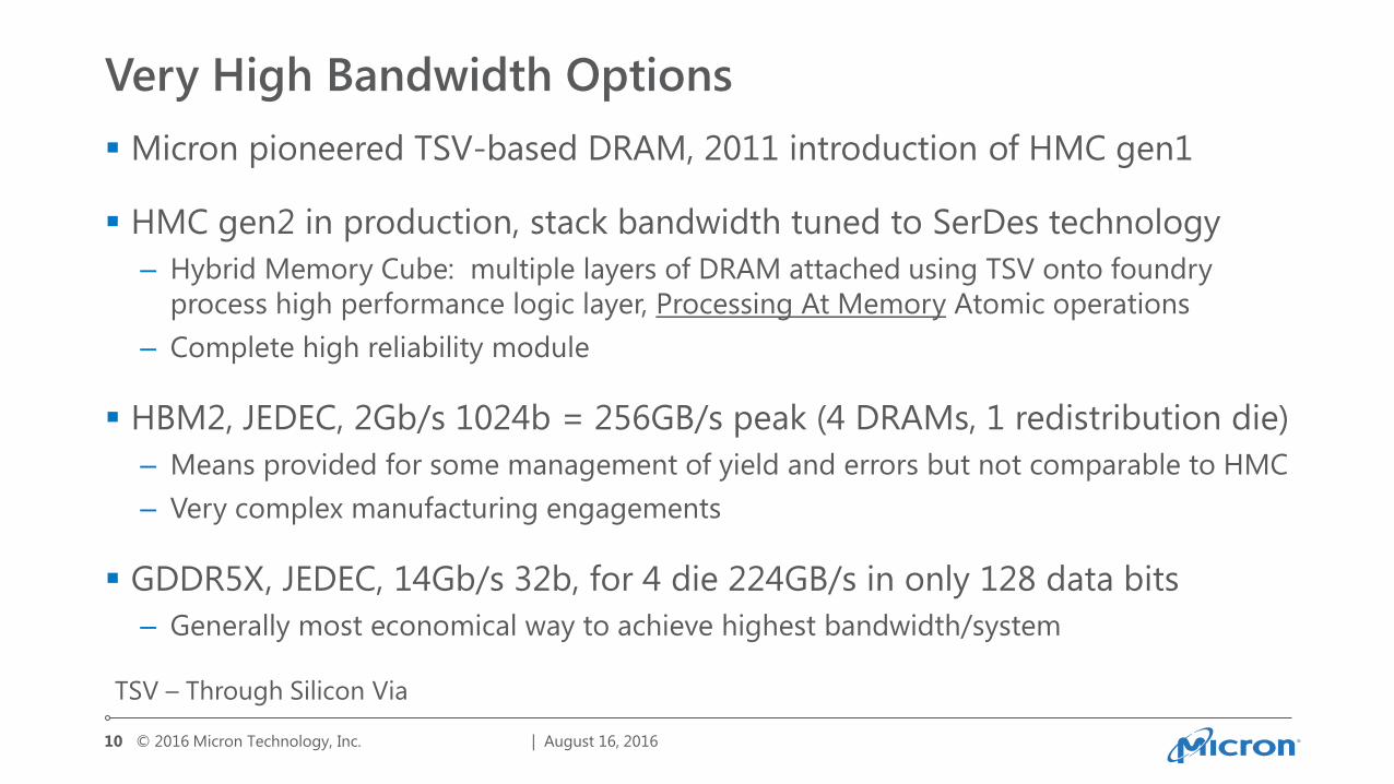
Very High Bandwidth Options
Micron pioneered TSV-based DRAM, 2011 introduction of HMC gen1
HMC gen2 in production, stack bandwidth tuned to SerDes technology
– Hybrid Memory Cube: multiple layers of DRAM attached using TSV onto foundry
process high performance logic layer, Processing At Memory Atomic operations
– Complete high reliability module
HBM2, JEDEC, 2Gb/s 1024b = 256GB/s peak (4 DRAMs, 1 redistribution die)
– Means provided for some management of yield and errors but not comparable to HMC
– Very complex manufacturing engagements
GDDR5X, JEDEC, 14Gb/s 32b, for 4 die 224GB/s in only 128 data bits
– Generally most economical way to achieve highest bandwidth/system
| August 16, 2016 10
TSV – Through Silicon Via
© 2016 Micron Technology, Inc.
Title and Content
The primary layout
used for standard
slides. The
placeholder can be
used to create text,
tables, or charts.
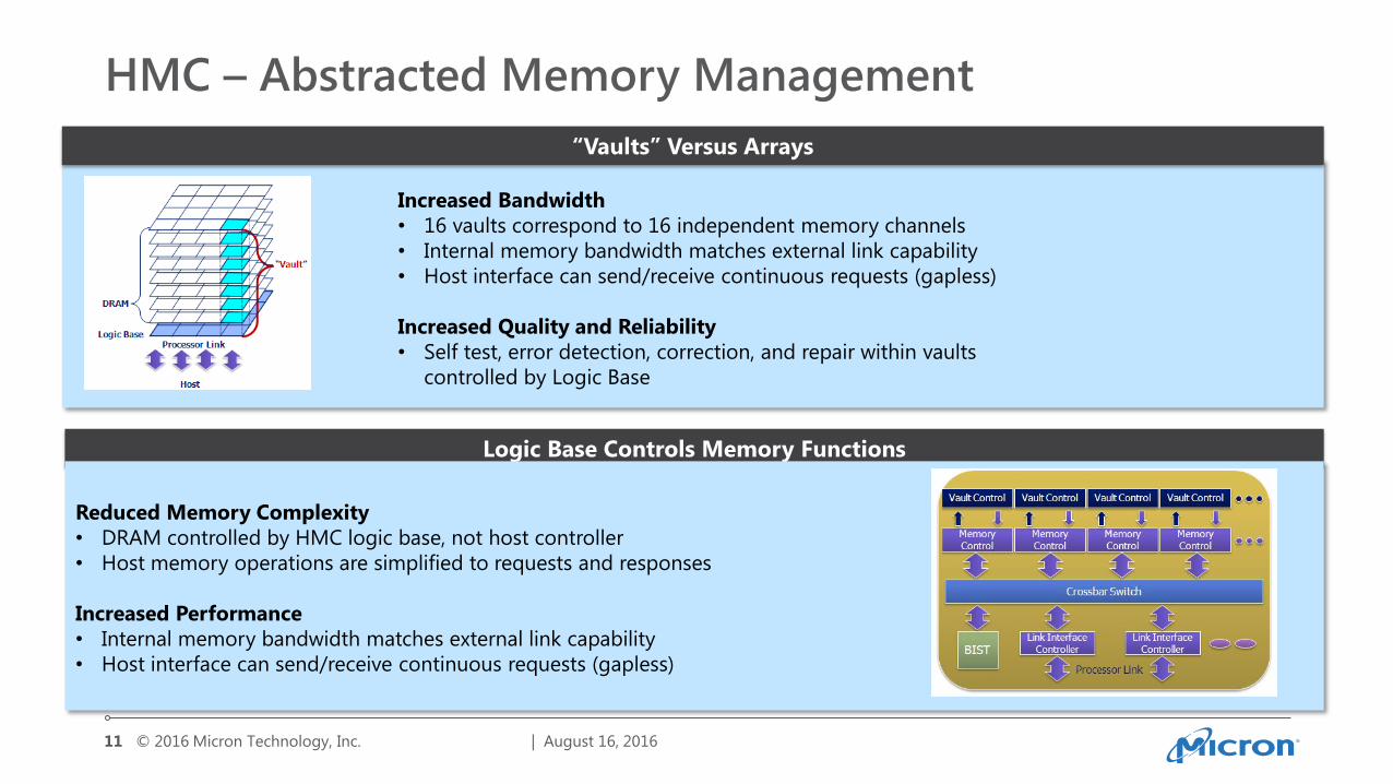
HMC – Abstracted Memory Management
| August 16, 2016 11
“Vaults” Versus Arrays
Logic Base Controls Memory Functions
Reduced Memory Complexity
• DRAM controlled by HMC logic base, not host controller
• Host memory operations are simplified to requests and responses
Increased Performance
• Internal memory bandwidth matches external link capability
• Host interface can send/receive continuous requests (gapless)
Increased Bandwidth
• 16 vaults correspond to 16 independent memory channels
• Internal memory bandwidth matches external link capability
• Host interface can send/receive continuous requests (gapless)
Increased Quality and Reliability
• Self test, error detection, correction, and repair within vaults
controlled by Logic Base
© 2016 Micron Technology, Inc.
Title and Content
The primary layout
used for standard
slides. The
placeholder can be
used to create text,
tables, or charts.
HMC – Reliability and Utility
Extraordinary Reliability, Availability and Serviceability (RAS) Features
Scrubbing, Correction of soft errors, In-Field Repair of hard errors
Error and Warning reporting through in-band or side-band options
Strong link CRC protection and retry mechanism
– Much higher correctness certainty than JEDEC adopted CRCs
Packet integrity checked before operations
Internal signals between logic layer and DRAM also protected
Atomic operations for application acceleration
– Observed 2-4x additional speedup beyond performance improvement from bandwidth
Scale-out capability: device chaining, networks of HMCs, etc.
| August 16, 2016 12
© 2016 Micron Technology, Inc.
Title and Content
The primary layout
used for standard
slides. The
placeholder can be
used to create text,
tables, or charts.
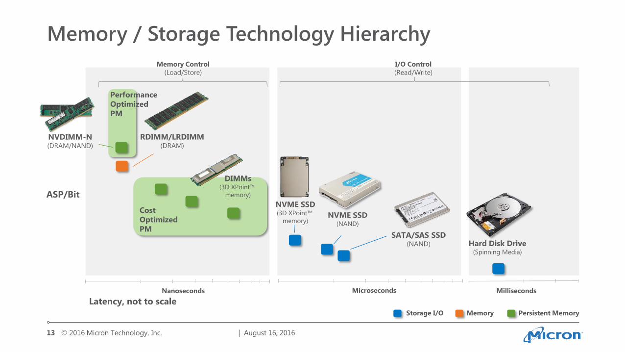
Memory / Storage Technology Hierarchy
| August 16, 2016 13
Nanoseconds Microseconds Milliseconds
Storage I/O Memory Persistent Memory
Memory Control
(Load/Store)
I/O Control
(Read/Write)
Hard Disk Drive (Spinning Media)
SATA/SAS SSD (NAND)
NVME SSD (NAND)
NVME SSD (3D XPoint™
memory)
DIMMs (3D XPoint™
memory) ASP/Bit
Latency, not to scale
NVDIMM-N (DRAM/NAND)
RDIMM/LRDIMM (DRAM)
Cost
Optimized
PM
Performance
Optimized
PM
© 2016 Micron Technology, Inc.
Title and Content
The primary layout
used for standard
slides. The
placeholder can be
used to create text,
tables, or charts.
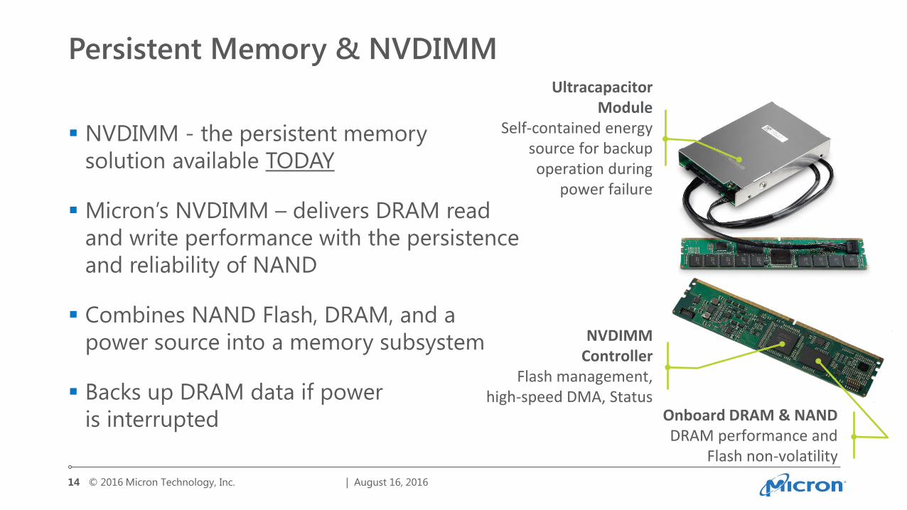
Persistent Memory & NVDIMM
NVDIMM - the persistent memory
solution available TODAY
Micron’s NVDIMM – delivers DRAM read
and write performance with the persistence
and reliability of NAND
Combines NAND Flash, DRAM, and a
power source into a memory subsystem
Backs up DRAM data if power
is interrupted
| August 16, 2016 14
Ultracapacitor Module
Self-contained energy source for backup operation during
power failure
NVDIMM Controller
Flash management, high-speed DMA, Status
Onboard DRAM & NAND DRAM performance and
Flash non-volatility
© 2016 Micron Technology, Inc.
Title and Content
The primary layout
used for standard
slides. The
placeholder can be
used to create text,
tables, or charts.
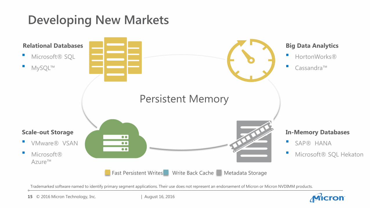
Developing New Markets
| August 16, 2016 15
Fast Persistent Writes Metadata Storage Write Back Cache
Scale-out Storage
VMware® VSAN
Microsoft®
Azure™
Big Data Analytics
HortonWorks®
Cassandra™
Persistent Memory
Relational Databases
Microsoft® SQL
MySQL™
Trademarked software named to identify primary segment applications. Their use does not represent an endorsement of Micron or Micron NVDIMM products.
In-Memory Databases
SAP® HANA
Microsoft® SQL Hekaton
© 2016 Micron Technology, Inc.
Title and Content
The primary layout
used for standard
slides. The
placeholder can be
used to create text,
tables, or charts.
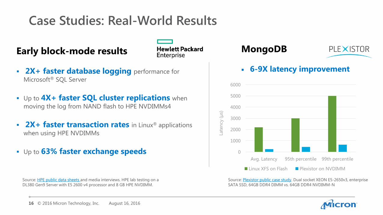
Case Studies: Real-World Results
August 16, 2016 16
Early block-mode results
2X+ faster database logging performance for
Microsoft® SQL Server
Up to 4X+ faster SQL cluster replications when
moving the log from NAND flash to HPE NVDIMMs4
2X+ faster transaction rates in Linux® applications
when using HPE NVDIMMs
Up to 63% faster exchange speeds
Source: HPE public data sheets and media interviews. HPE lab testing on a
DL380 Gen9 Server with E5 2600 v4 processor and 8 GB HPE NVDIMM.
Source: Plexistor public case study. Dual socket XEON E5-2650v3, enterprise
SATA SSD, 64GB DDR4 DIMM vs. 64GB DDR4 NVDIMM-N
MongoDB
6-9X latency improvement
0
1000
2000
3000
4000
5000
6000
Avg. Latency 95th percentile 99th percentile
Linux XFS on Flash Plexistor on NVDIMM
Late
ncy
(µ
s)
© 2016 Micron Technology, Inc.
Title and Content
The primary layout
used for standard
slides. The
placeholder can be
used to create text,
tables, or charts.
Future Mainstream Memory
Future graphics and low power DRAM architectures in work
DDR5 for ~2018 samples, ~2019 production, details subject to change
– 8-32Gb capacity, 3.2-6.4Gbps IO, 1.1V, 16n prefetch, 16-32 banks in 8 groups
– Basically 2x bandwidth of DDR4, some innovations at module level too
All good, but…
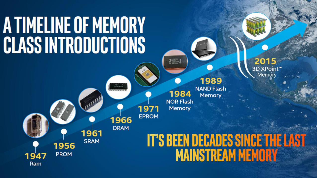
Most interesting is the new class of memory from Micron / Intel
August 16, 2016 17
© 2016 Micron Technology, Inc.
Title and Content
The primary layout
used for standard
slides. The
placeholder can be
used to create text,
tables, or charts.
August 16, 2016 18 | Micron Confidential
Memory
© 2016 Micron Technology, Inc.
Title and Content
The primary layout
used for standard
slides. The
placeholder can be
used to create text,
tables, or charts.
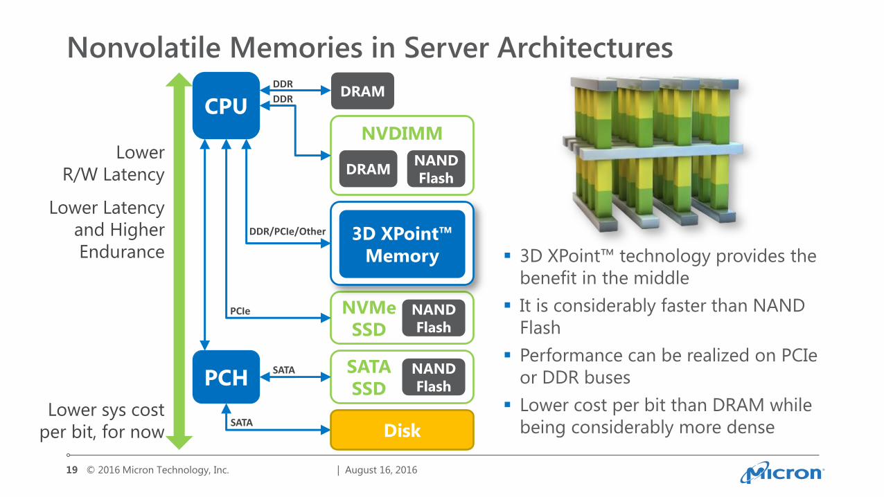
Nonvolatile Memories in Server Architectures
3D XPoint™ technology provides the
benefit in the middle
It is considerably faster than NAND
Flash
Performance can be realized on PCIe
or DDR buses
Lower cost per bit than DRAM while
being considerably more dense
| August 16, 2016 19
CPU
PCH SATA
SSD NAND
Flash
NVMe
SSD NAND
Flash
DRAM
NVDIMM
NAND
Flash DRAM
3D XPoint™
Memory
DDR
DDR
DDR/PCIe/Other
PCIe
SATA
SATA
Lower
R/W Latency
Lower Latency
and Higher
Endurance
Lower sys cost
per bit, for now Disk
© 2016 Micron Technology, Inc.
Title and Content
The primary layout
used for standard
slides. The
placeholder can be
used to create text,
tables, or charts.
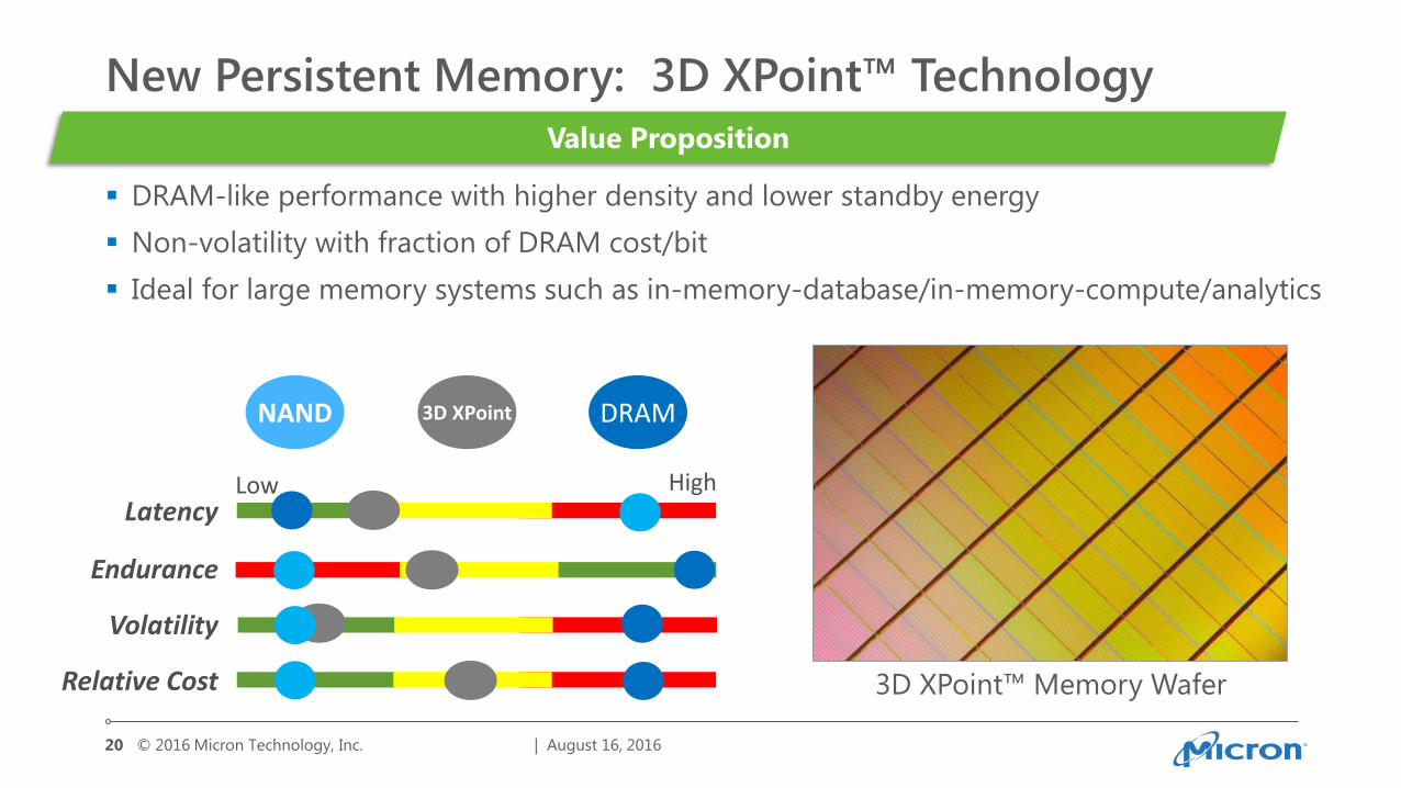
New Persistent Memory: 3D XPoint™ Technology
DRAM-like performance with higher density and lower standby energy
Non-volatility with fraction of DRAM cost/bit
Ideal for large memory systems such as in-memory-database/in-memory-compute/analytics
| August 16, 2016 20
Value Proposition
Latency
DRAM NAND 3D XPoint
Endurance
Volatility
Relative Cost
Low High
3D XPoint™ Memory Wafer
© 2016 Micron Technology, Inc.
Title and Content
The primary layout
used for standard
slides. The
placeholder can be
used to create text,
tables, or charts.
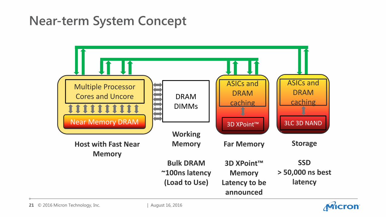
Near-term System Concept
| August 16, 2016 21
DRAM DIMMs
Multiple Processor Cores and Uncore
Host with Fast Near Memory
Storage
SSD > 50,000 ns best
latency
3D XPoint™
ASICs and DRAM
caching
Far Memory
3D XPoint™ Memory
Latency to be announced
Working Memory
Bulk DRAM
~100ns latency (Load to Use)
Near Memory DRAM 3LC 3D NAND
ASICs and DRAM
caching
© 2016 Micron Technology, Inc.
Title and Content
The primary layout
used for standard
slides. The
placeholder can be
used to create text,
tables, or charts.
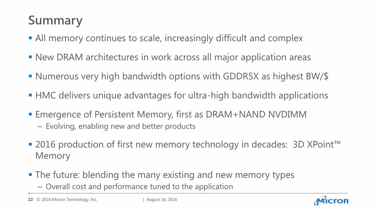
Summary
All memory continues to scale, increasingly difficult and complex
New DRAM architectures in work across all major application areas
Numerous very high bandwidth options with GDDR5X as highest BW/$
HMC delivers unique advantages for ultra-high bandwidth applications
Emergence of Persistent Memory, first as DRAM+NAND NVDIMM
– Evolving, enabling new and better products
2016 production of first new memory technology in decades: 3D XPoint™
Memory
The future: blending the many existing and new memory types
– Overall cost and performance tuned to the application
| August 16, 2016 22
Blue Ending Slide