Embed Size (px)
Citation preview
MELSEC iQ-FFX5 User's Manual (Temperature Control)

SAFETY PRECAUTIONS(Read these precautions before use.)
Before using this product, please read this manual and the relevant manuals introduced in this manual carefully and pay full
attention to safety in order to handle the product correctly.
This manual classifies the safety precautions into two categories: [ WARNING] and [ CAUTION].
Depending on the circumstances, procedures indicated by [ CAUTION] may also cause severe injury.
It is important to follow all precautions for personal safety.
Store this manual in a safe place so that it can be read whenever necessary. Always forward it to the end user.
[DESIGN PRECAUTIONS]
WARNING● Make sure to set up the following safety circuits outside the PLC to ensure safe system operation
even during external power supply problems or PLC failure. Otherwise, malfunctions may cause
serious accidents.
- Most importantly, set up the following: an emergency stop circuit, a protection circuit, an interlock
circuit for opposite movements (such as normal vs. reverse rotation), and an interlock circuit to
prevent damage (to the equipment at the upper and lower positioning limits).
- Note that when the CPU module detects an error, such as a watchdog timer error, during self-
diagnosis, all outputs are turned off. Also, when an error that cannot be detected by the CPU
module occurs in an input/output control block, output control may be disabled. External circuits
and mechanisms should be designed to ensure safe machinery operation in such a case.
- Note that when an error occurs in a relay, transistor or triac of an output circuit, the output might
stay on or off. For output signals that may lead to serious accidents, external circuits and
mechanisms should be designed to ensure safe machinery operation in such a case.
● In an output circuit, when a load current exceeding the current rating or an overcurrent caused by a
load short-circuit flows for a long time, it may cause smoke and fire. To prevent this, configure an
external safety circuit, such as a fuse.
● Construct an interlock circuit in the program so that the whole system always operates on the safe
side before executing the control (for data change) of the PLC in operation.
Read the manual thoroughly and ensure complete safety before executing other controls (for program
change, parameter change, forcible output and operation status change) of the PLC in operation.
Otherwise, the machine may be damaged and accidents may occur due to erroneous operations.
● Do not write any data to the "system area" and "write-protect area" of the buffer memory in the
module. Executing data writing to the "system area" or "write protect area" may cause malfunction of
the programmable controller alarm. For the "system area" or "write-protect area", refer to Page 99
Buffer Memory Areas.
WARNING Indicates that incorrect handling may cause hazardous conditions, resulting in death or severe injury.
CAUTION Indicates that incorrect handling may cause hazardous conditions, resulting in minor or moderate injury or property damage.
1
2
[DESIGN PRECAUTIONS]
[INSTALLATION PRECAUTIONS]
CAUTION● When an inductive load such as a lamp, heater, or solenoid valve is controlled, a large current
(approximately ten times greater than normal) may flow when the output is turned from off to on.
Take proper measures so that the flowing current dose not exceed the value corresponding to the
maximum load specification of the resistance load.
● Simultaneously turn on and off the power supplies of the CPU module and extension modules.
WARNING● Make sure to cut off all phases of the power supply externally before attempting installation or wiring
work. Failure to do so may cause electric shock or damage to the product.
● This product is an open type device that must be installed and used within a control cabinet which
satisfies all of the following three requirements.
- a cabinet which has conductivity.
- a cabinet which has a structure to prevent the fire to spread outside the cabinet.
- a cabinet which has sufficient mechanical strength.
● Use the product within the generic environment specifications described in the User's Manual
(Hardware) of the CPU module used.
Never use the product in areas with excessive dust, oily smoke, conductive dusts, corrosive gas (salt
air, Cl2, H2S, SO2 or NO2), flammable gas, vibration or impacts, or expose it to high temperature,
condensation, or rain and wind.
If the product is used in such conditions, electric shock, fire, malfunctions, deterioration or damage
may occur.
[INSTALLATION PRECAUTIONS]
[WIRING PRECAUTIONS]
CAUTION● Do not touch the conductive parts of the product directly. Doing so may cause device failures or
malfunctions.
● When drilling screw holes or wiring, make sure that cutting and wiring debris do not enter the
ventilation slits of the PLC. Failure to do so may cause fire, equipment failures or malfunctions.
● For the product supplied together with a dust proof sheet, the sheet should be affixed to the ventilation
slits before the installation and wiring work to prevent foreign objects such as cutting and wiring
debris.
However, when the installation work is completed, make sure to remove the sheet to provide
adequate ventilation. Failure to do so may cause fire, equipment failures or malfunctions.
● Install the product on a flat surface. If the mounting surface is rough, undue force will be applied to the
PC board, thereby causing nonconformities.
● Install the product securely using a DIN rail or mounting screws.
● Work carefully when using a screwdriver such as installation of the product. Failure to do so may
cause damage to the product or accidents.
● Connect the extension cables, peripheral device cables, input/output cables and battery connecting
cable securely to their designated connectors. Loose connections may cause malfunctions.
● Turn off the power to the PLC before attaching or detaching the following devices. Failure to do so
may cause device failures or malfunctions.
- Peripheral devices, expansion board, expansion adapter, and connector conversion adapter
- Extension modules, bus conversion module, and connector conversion module
- Battery
WARNING● Make sure to cut off all phases of the power supply externally before attempting installation or wiring
work. Failure to do so may cause electric shock or damage to the product.
● Make sure to attach the terminal cover, provided as an accessory, before turning on the power or
initiating operation after installation or wiring work. Failure to do so may cause electric shock.
● Don't use the input terminals for measurement on a main circuit, since those terminals have no
measurement category.
● The temperature rating of the cable should be 80 or more.
● Make sure to properly wire to the spring clamp terminal block in accordance with the following
precautions. Failure to do so may cause electric shock, equipment failures, a short-circuit, wire
breakage, malfunctions, or damage to the product.
- The disposal size of the cable end should follow the dimensions described in the manual.
- Twist the ends of stranded wires and make sure that there are no loose wires.
- Do not solder-plate the electric wire ends.
- Do not connect more than the specified number of wires or electric wires of unspecified size.
- Affix the electric wires so that neither the terminal block nor the connected parts are directly
stressed.
3
4
[WIRING PRECAUTIONS]
[STARTUP AND MAINTENANCE PRECAUTIONS]
CAUTION● Perform class D grounding (grounding resistance: 100 Ω or less) of the grounding terminal on the
CPU module and extension modules with a wire 2 mm2 or thicker.
Do not use common grounding with heavy electrical systems (Page 73 Grounding).
● Connect the power supply wiring to the dedicated terminals described in this manual. If an AC power
supply is connected to a DC input/output terminal or DC power supply terminal, the PLC will burn out.
● Do not wire vacant terminals externally. Doing so may damage the product.
● Install module so that excessive force will not be applied to terminal blocks, power connectors, I/O
connectors, communication connectors, or communication cables. Failure to do so may result in wire
damage/breakage or PLC failure.
● Make sure to observe the following precautions in order to prevent any damage to the machinery or
accidents due to malfunction of the PLC caused by abnormal data written to the PLC due to the
effects of noise:
- Do not bundle the power line, control line and communication cables together with or lay them
close to the main circuit, high-voltage line, load line or power line. As a guideline, lay the power
line, control line and connection cables at least 100 mm away from the main circuit, high-voltage
line, load line or power line.
- Ground the shield of the analog input/output cable at one point on the signal receiving side.
However, do not use common grounding with heavy electrical systems.
● Check the interface type and correctly connect the cable. Incorrect wiring (connecting the cable to an
incorrect interface) may cause failure of the module and external device.
● To terminal blocks or power connectors, connect circuits isolated from hazardous voltage by double/
reinforced insulation.
WARNING● Do not touch any terminal while the PLC's power is on. Doing so may cause electric shock or
malfunctions.
● Before cleaning or retightening terminals, cut off all phases of the power supply externally. Failure to
do so in the power ON status may cause electric shock.
● Before modifying the program in operation, forcible output, running or stopping the PLC, read through
this manual carefully, and ensure complete safety. An operation error may damage the machinery or
cause accidents.
● Do not change the program in the PLC from two or more peripheral equipment devices at the same
time. (i. e. from an engineering tool and a GOT) Doing so may cause destruction or malfunction of the
PLC program.
[STARTUP AND MAINTENANCE PRECAUTIONS]
[OPERATION PRECAUTIONS]
[DISPOSAL PRECAUTIONS]
[TRANSPORTATION PRECAUTIONS]
CAUTION● Do not disassemble or modify the PLC. Doing so may cause fire, equipment failures, or malfunctions.
For repair, contact your local Mitsubishi Electric representative.
● Turn off the power to the PLC before connecting or disconnecting any extension cable. Failure to do
so may cause device failures or malfunctions.
● Turn off the power to the PLC before attaching or detaching the following devices. Failure to do so
may cause device failures or malfunctions.
- Peripheral devices, expansion board, expansion adapter, and connector conversion adapter
- Extension modules, bus conversion module, and connector conversion module
- Battery
CAUTION● Construct an interlock circuit in the program so that the whole system always operates on the safe
side before executing the control (for data change) of the PLC in operation. Read the manual
thoroughly and ensure complete safety before executing other controls (for program change,
parameter change, forcible output and operation status change) of the PLC in operation. Otherwise,
the machine may be damaged and accidents may occur by erroneous operations.
CAUTION● Please contact a certified electronic waste disposal company for the environmentally safe recycling
and disposal of your device.
CAUTION● The PLC is a precision instrument. During transportation, avoid impacts larger than those specified in
the general specifications of the User's Manual (Hardware) of the CPU module used by using
dedicated packaging boxes and shock-absorbing palettes. Failure to do so may cause failures in the
PLC. After transportation, verify operation of the PLC and check for damage of the mounting part, etc.
5
6
INTRODUCTIONThis manual contains text, diagrams and explanations which will guide the reader in the correct installation, safe use and
operation of the temperature control module of MELSEC iQ-F series and should be read and understood before attempting to
install or use the module.
Always forward it to the end user.
Regarding use of this product • This product has been manufactured as a general-purpose part for general industries, and has not been designed or
manufactured to be incorporated in a device or system used in purposes related to human life.
• Before using the product for special purposes such as nuclear power, electric power, aerospace, medicine or passenger
movement vehicles, consult Mitsubishi Electric.
• This product has been manufactured under strict quality control. However when installing the product where major
accidents or losses could occur if the product fails, install appropriate backup or failsafe functions in the system.
Note • If in doubt at any stage during the installation of the product, always consult a professional electrical engineer who is
qualified and trained in the local and national standards. If in doubt about the operation or use, please consult the nearest
Mitsubishi Electric representative.
• Since the examples indicated by this manual, technical bulletin, catalog, etc. are used as a reference, please use it after
confirming the function and safety of the equipment and system. Mitsubishi Electric will accept no responsibility for actual
use of the product based on these illustrative examples.
• This manual content, specification etc. may be changed, without a notice, for improvement.
• The information in this manual has been carefully checked and is believed to be accurate; however, if you notice a doubtful
point, an error, etc., please contact the nearest Mitsubishi Electric representative. When doing so, please provide the
manual number given at the end of this manual.

MEMO
7
8
CONTENTSSAFETY PRECAUTIONS . . . . . . . . . . . . . . . . . . . . . . . . . . . . . . . . . . . . . . . . . . . . . . . . . . . . . . . . . . . . . . . . . . . .1
INTRODUCTION. . . . . . . . . . . . . . . . . . . . . . . . . . . . . . . . . . . . . . . . . . . . . . . . . . . . . . . . . . . . . . . . . . . . . . . . . . .6
RELEVANT MANUALS . . . . . . . . . . . . . . . . . . . . . . . . . . . . . . . . . . . . . . . . . . . . . . . . . . . . . . . . . . . . . . . . . . . . .12
TERMS . . . . . . . . . . . . . . . . . . . . . . . . . . . . . . . . . . . . . . . . . . . . . . . . . . . . . . . . . . . . . . . . . . . . . . . . . . . . . . . . .13
CHAPTER 1 DESCRIPTION 15
CHAPTER 2 SPECIFICATIONS 16
2.1 General Specifications . . . . . . . . . . . . . . . . . . . . . . . . . . . . . . . . . . . . . . . . . . . . . . . . . . . . . . . . . . . . . . . . . . . 16
2.2 Power Supply Specifications . . . . . . . . . . . . . . . . . . . . . . . . . . . . . . . . . . . . . . . . . . . . . . . . . . . . . . . . . . . . . . 16
2.3 Performance Specifications . . . . . . . . . . . . . . . . . . . . . . . . . . . . . . . . . . . . . . . . . . . . . . . . . . . . . . . . . . . . . . . 16
Input specifications . . . . . . . . . . . . . . . . . . . . . . . . . . . . . . . . . . . . . . . . . . . . . . . . . . . . . . . . . . . . . . . . . . . . . . . 17
Measurement precision . . . . . . . . . . . . . . . . . . . . . . . . . . . . . . . . . . . . . . . . . . . . . . . . . . . . . . . . . . . . . . . . . . . . 17
Current detector (CT) input specifications . . . . . . . . . . . . . . . . . . . . . . . . . . . . . . . . . . . . . . . . . . . . . . . . . . . . . . 18
Process values . . . . . . . . . . . . . . . . . . . . . . . . . . . . . . . . . . . . . . . . . . . . . . . . . . . . . . . . . . . . . . . . . . . . . . . . . . 19
Process temperature range . . . . . . . . . . . . . . . . . . . . . . . . . . . . . . . . . . . . . . . . . . . . . . . . . . . . . . . . . . . . . . . . . 19
Output specifications . . . . . . . . . . . . . . . . . . . . . . . . . . . . . . . . . . . . . . . . . . . . . . . . . . . . . . . . . . . . . . . . . . . . . . 19
2.4 Part Names. . . . . . . . . . . . . . . . . . . . . . . . . . . . . . . . . . . . . . . . . . . . . . . . . . . . . . . . . . . . . . . . . . . . . . . . . . . . . 20
LED display . . . . . . . . . . . . . . . . . . . . . . . . . . . . . . . . . . . . . . . . . . . . . . . . . . . . . . . . . . . . . . . . . . . . . . . . . . . . . 20
CHAPTER 3 PROCEDURES BEFORE OPERATION 21
CHAPTER 4 FUNCTION 22
4.1 Functions list . . . . . . . . . . . . . . . . . . . . . . . . . . . . . . . . . . . . . . . . . . . . . . . . . . . . . . . . . . . . . . . . . . . . . . . . . . . 22
4.2 Control Mode Selection Function . . . . . . . . . . . . . . . . . . . . . . . . . . . . . . . . . . . . . . . . . . . . . . . . . . . . . . . . . . 24
4.3 Control Method . . . . . . . . . . . . . . . . . . . . . . . . . . . . . . . . . . . . . . . . . . . . . . . . . . . . . . . . . . . . . . . . . . . . . . . . . 26
4.4 Manual Control . . . . . . . . . . . . . . . . . . . . . . . . . . . . . . . . . . . . . . . . . . . . . . . . . . . . . . . . . . . . . . . . . . . . . . . . . 30
4.5 Balance Bumpless Function . . . . . . . . . . . . . . . . . . . . . . . . . . . . . . . . . . . . . . . . . . . . . . . . . . . . . . . . . . . . . . 31
4.6 RFB Limiter Function . . . . . . . . . . . . . . . . . . . . . . . . . . . . . . . . . . . . . . . . . . . . . . . . . . . . . . . . . . . . . . . . . . . . 31
4.7 Simple Two-degree-of-freedom . . . . . . . . . . . . . . . . . . . . . . . . . . . . . . . . . . . . . . . . . . . . . . . . . . . . . . . . . . . . 32
4.8 Normal/Reverse Operation Selection Function . . . . . . . . . . . . . . . . . . . . . . . . . . . . . . . . . . . . . . . . . . . . . . . 32
4.9 Proportional Band Setting Function . . . . . . . . . . . . . . . . . . . . . . . . . . . . . . . . . . . . . . . . . . . . . . . . . . . . . . . . 33
4.10 Overlap/dead Band Function . . . . . . . . . . . . . . . . . . . . . . . . . . . . . . . . . . . . . . . . . . . . . . . . . . . . . . . . . . . . . . 34
4.11 Cooling Method Setting Function . . . . . . . . . . . . . . . . . . . . . . . . . . . . . . . . . . . . . . . . . . . . . . . . . . . . . . . . . . 35
4.12 Auto Tuning Function . . . . . . . . . . . . . . . . . . . . . . . . . . . . . . . . . . . . . . . . . . . . . . . . . . . . . . . . . . . . . . . . . . . . 36
4.13 AT (Auto Tuning) Bias Function. . . . . . . . . . . . . . . . . . . . . . . . . . . . . . . . . . . . . . . . . . . . . . . . . . . . . . . . . . . . 40
4.14 Startup Tuning Function . . . . . . . . . . . . . . . . . . . . . . . . . . . . . . . . . . . . . . . . . . . . . . . . . . . . . . . . . . . . . . . . . . 41
4.15 Operations Mode Selection Function . . . . . . . . . . . . . . . . . . . . . . . . . . . . . . . . . . . . . . . . . . . . . . . . . . . . . . . 43
4.16 Cascade Control . . . . . . . . . . . . . . . . . . . . . . . . . . . . . . . . . . . . . . . . . . . . . . . . . . . . . . . . . . . . . . . . . . . . . . . . 44
4.17 SV Tracking Function . . . . . . . . . . . . . . . . . . . . . . . . . . . . . . . . . . . . . . . . . . . . . . . . . . . . . . . . . . . . . . . . . . . . 46
4.18 Settings Limiter Function . . . . . . . . . . . . . . . . . . . . . . . . . . . . . . . . . . . . . . . . . . . . . . . . . . . . . . . . . . . . . . . . . 46
4.19 Setting Change Rate Limiter Setting Function . . . . . . . . . . . . . . . . . . . . . . . . . . . . . . . . . . . . . . . . . . . . . . . . 47
4.20 Input Type Selection Function . . . . . . . . . . . . . . . . . . . . . . . . . . . . . . . . . . . . . . . . . . . . . . . . . . . . . . . . . . . . . 47
4.21 Sensor Correction Function . . . . . . . . . . . . . . . . . . . . . . . . . . . . . . . . . . . . . . . . . . . . . . . . . . . . . . . . . . . . . . . 48
4.22 Primary Delay Digital Filter. . . . . . . . . . . . . . . . . . . . . . . . . . . . . . . . . . . . . . . . . . . . . . . . . . . . . . . . . . . . . . . . 49
4.23 Temperature Rise Judgment Function . . . . . . . . . . . . . . . . . . . . . . . . . . . . . . . . . . . . . . . . . . . . . . . . . . . . . . 50
4.24 External (Other Analog Module) I/O Function. . . . . . . . . . . . . . . . . . . . . . . . . . . . . . . . . . . . . . . . . . . . . . . . . 50
4.25 Output Limiter Function . . . . . . . . . . . . . . . . . . . . . . . . . . . . . . . . . . . . . . . . . . . . . . . . . . . . . . . . . . . . . . . . . . 51
CO
NT
EN
TS
4.26 Output Change Ratio Limiter Function . . . . . . . . . . . . . . . . . . . . . . . . . . . . . . . . . . . . . . . . . . . . . . . . . . . . . . 52
4.27 Control Output Flag. . . . . . . . . . . . . . . . . . . . . . . . . . . . . . . . . . . . . . . . . . . . . . . . . . . . . . . . . . . . . . . . . . . . . . 52
4.28 Transistor Outputs Selection Function . . . . . . . . . . . . . . . . . . . . . . . . . . . . . . . . . . . . . . . . . . . . . . . . . . . . . . 53
4.29 Alert Function . . . . . . . . . . . . . . . . . . . . . . . . . . . . . . . . . . . . . . . . . . . . . . . . . . . . . . . . . . . . . . . . . . . . . . . . . . 54
4.30 Loop Disconnection Detection Function . . . . . . . . . . . . . . . . . . . . . . . . . . . . . . . . . . . . . . . . . . . . . . . . . . . . 61
4.31 Loop Disconnection Detection Dead Band Function. . . . . . . . . . . . . . . . . . . . . . . . . . . . . . . . . . . . . . . . . . . 62
4.32 Heater Disconnection Detection Function . . . . . . . . . . . . . . . . . . . . . . . . . . . . . . . . . . . . . . . . . . . . . . . . . . . 63
4.33 Output OFF-time Current Error Detection Function. . . . . . . . . . . . . . . . . . . . . . . . . . . . . . . . . . . . . . . . . . . . 63
4.34 Buffer Memory Data Backup Function . . . . . . . . . . . . . . . . . . . . . . . . . . . . . . . . . . . . . . . . . . . . . . . . . . . . . . 64
4.35 Default Function . . . . . . . . . . . . . . . . . . . . . . . . . . . . . . . . . . . . . . . . . . . . . . . . . . . . . . . . . . . . . . . . . . . . . . . . 65
4.36 Error History Function . . . . . . . . . . . . . . . . . . . . . . . . . . . . . . . . . . . . . . . . . . . . . . . . . . . . . . . . . . . . . . . . . . . 65
4.37 FX3 Allocation Mode Function . . . . . . . . . . . . . . . . . . . . . . . . . . . . . . . . . . . . . . . . . . . . . . . . . . . . . . . . . . . . . 68
CHAPTER 5 SYSTEM CONFIGURATION 69
5.1 Overall Configuration . . . . . . . . . . . . . . . . . . . . . . . . . . . . . . . . . . . . . . . . . . . . . . . . . . . . . . . . . . . . . . . . . . . . 69
CHAPTER 6 WIRING 70
6.1 Spring Clamp Terminal Block. . . . . . . . . . . . . . . . . . . . . . . . . . . . . . . . . . . . . . . . . . . . . . . . . . . . . . . . . . . . . . 70
6.2 Terminals Layout . . . . . . . . . . . . . . . . . . . . . . . . . . . . . . . . . . . . . . . . . . . . . . . . . . . . . . . . . . . . . . . . . . . . . . . . 72
6.3 Power Supply Wiring. . . . . . . . . . . . . . . . . . . . . . . . . . . . . . . . . . . . . . . . . . . . . . . . . . . . . . . . . . . . . . . . . . . . . 73
Grounding . . . . . . . . . . . . . . . . . . . . . . . . . . . . . . . . . . . . . . . . . . . . . . . . . . . . . . . . . . . . . . . . . . . . . . . . . . . . . . 73
6.4 External Wiring Example . . . . . . . . . . . . . . . . . . . . . . . . . . . . . . . . . . . . . . . . . . . . . . . . . . . . . . . . . . . . . . . . . 74
CHAPTER 7 PARAMETER SETTING 77
7.1 Base Setting. . . . . . . . . . . . . . . . . . . . . . . . . . . . . . . . . . . . . . . . . . . . . . . . . . . . . . . . . . . . . . . . . . . . . . . . . . . . 77
7.2 Application Setting . . . . . . . . . . . . . . . . . . . . . . . . . . . . . . . . . . . . . . . . . . . . . . . . . . . . . . . . . . . . . . . . . . . . . . 78
7.3 CT Setting. . . . . . . . . . . . . . . . . . . . . . . . . . . . . . . . . . . . . . . . . . . . . . . . . . . . . . . . . . . . . . . . . . . . . . . . . . . . . . 79
7.4 Refresh Setting . . . . . . . . . . . . . . . . . . . . . . . . . . . . . . . . . . . . . . . . . . . . . . . . . . . . . . . . . . . . . . . . . . . . . . . . . 80
CHAPTER 8 PROGRAMMING 81
8.1 Programming Procedure . . . . . . . . . . . . . . . . . . . . . . . . . . . . . . . . . . . . . . . . . . . . . . . . . . . . . . . . . . . . . . . . . 81
Standard PID control . . . . . . . . . . . . . . . . . . . . . . . . . . . . . . . . . . . . . . . . . . . . . . . . . . . . . . . . . . . . . . . . . . . . . . 81
Heating-cooling PID control. . . . . . . . . . . . . . . . . . . . . . . . . . . . . . . . . . . . . . . . . . . . . . . . . . . . . . . . . . . . . . . . . 87
CHAPTER 9 TROUBLESHOOTING 90
9.1 Checks with LEDs . . . . . . . . . . . . . . . . . . . . . . . . . . . . . . . . . . . . . . . . . . . . . . . . . . . . . . . . . . . . . . . . . . . . . . . 90
The POWER LED has turned OFF . . . . . . . . . . . . . . . . . . . . . . . . . . . . . . . . . . . . . . . . . . . . . . . . . . . . . . . . . . . 90
The RUN LED has turned OFF . . . . . . . . . . . . . . . . . . . . . . . . . . . . . . . . . . . . . . . . . . . . . . . . . . . . . . . . . . . . . . 90
When the ERROR LED turns on or flashes. . . . . . . . . . . . . . . . . . . . . . . . . . . . . . . . . . . . . . . . . . . . . . . . . . . . . 90
9.2 Checks When Trouble Occurs . . . . . . . . . . . . . . . . . . . . . . . . . . . . . . . . . . . . . . . . . . . . . . . . . . . . . . . . . . . . . 91
9.3 List of Error Codes . . . . . . . . . . . . . . . . . . . . . . . . . . . . . . . . . . . . . . . . . . . . . . . . . . . . . . . . . . . . . . . . . . . . . . 92
9.4 List of Alarm Codes. . . . . . . . . . . . . . . . . . . . . . . . . . . . . . . . . . . . . . . . . . . . . . . . . . . . . . . . . . . . . . . . . . . . . . 94
APPENDICES 95
Appendix 1 External Dimensions . . . . . . . . . . . . . . . . . . . . . . . . . . . . . . . . . . . . . . . . . . . . . . . . . . . . . . . . . . . . . . . . 95
Appendix 2 Standards . . . . . . . . . . . . . . . . . . . . . . . . . . . . . . . . . . . . . . . . . . . . . . . . . . . . . . . . . . . . . . . . . . . . . . . . . 96
Certification of UL, cUL standards. . . . . . . . . . . . . . . . . . . . . . . . . . . . . . . . . . . . . . . . . . . . . . . . . . . . . . . . . . . . 96
Compliance with EC directive (CE Marking) . . . . . . . . . . . . . . . . . . . . . . . . . . . . . . . . . . . . . . . . . . . . . . . . . . . . 96
Requirement for compliance with EMC directive. . . . . . . . . . . . . . . . . . . . . . . . . . . . . . . . . . . . . . . . . . . . . . . . . 96
Appendix 3 Module Label . . . . . . . . . . . . . . . . . . . . . . . . . . . . . . . . . . . . . . . . . . . . . . . . . . . . . . . . . . . . . . . . . . . . . . 98
9
10
Appendix 4 Buffer Memory Areas. . . . . . . . . . . . . . . . . . . . . . . . . . . . . . . . . . . . . . . . . . . . . . . . . . . . . . . . . . . . . . . . 99
List of buffer memory addresses . . . . . . . . . . . . . . . . . . . . . . . . . . . . . . . . . . . . . . . . . . . . . . . . . . . . . . . . . . . . . 99
Details of buffer memory addresses . . . . . . . . . . . . . . . . . . . . . . . . . . . . . . . . . . . . . . . . . . . . . . . . . . . . . . . . . 117
Appendix 5 PID . . . . . . . . . . . . . . . . . . . . . . . . . . . . . . . . . . . . . . . . . . . . . . . . . . . . . . . . . . . . . . . . . . . . . . . . . . . . . . 166
PID operations. . . . . . . . . . . . . . . . . . . . . . . . . . . . . . . . . . . . . . . . . . . . . . . . . . . . . . . . . . . . . . . . . . . . . . . . . . 166
Actions of the temperature control module . . . . . . . . . . . . . . . . . . . . . . . . . . . . . . . . . . . . . . . . . . . . . . . . . . . . 167
Proportional action (P action) . . . . . . . . . . . . . . . . . . . . . . . . . . . . . . . . . . . . . . . . . . . . . . . . . . . . . . . . . . . . . . 168
Integral action (I action) . . . . . . . . . . . . . . . . . . . . . . . . . . . . . . . . . . . . . . . . . . . . . . . . . . . . . . . . . . . . . . . . . . . 169
Derivative action (D action) . . . . . . . . . . . . . . . . . . . . . . . . . . . . . . . . . . . . . . . . . . . . . . . . . . . . . . . . . . . . . . . . 170
PID action . . . . . . . . . . . . . . . . . . . . . . . . . . . . . . . . . . . . . . . . . . . . . . . . . . . . . . . . . . . . . . . . . . . . . . . . . . . . . 170
INDEX 171
REVISIONS. . . . . . . . . . . . . . . . . . . . . . . . . . . . . . . . . . . . . . . . . . . . . . . . . . . . . . . . . . . . . . . . . . . . . . . . . . . . .174
WARRANTY . . . . . . . . . . . . . . . . . . . . . . . . . . . . . . . . . . . . . . . . . . . . . . . . . . . . . . . . . . . . . . . . . . . . . . . . . . . .175
TRADEMARKS . . . . . . . . . . . . . . . . . . . . . . . . . . . . . . . . . . . . . . . . . . . . . . . . . . . . . . . . . . . . . . . . . . . . . . . . . .176

CO
NT
EN
TS
11
12
RELEVANT MANUALSManual name <manual number> Description
MELSEC iQ-F FX5 User's Manual (Startup)
<JY997D58201>
Performance specifications, procedures before operation, and troubleshooting of the
CPU module.
MELSEC iQ-F FX5U User's Manual (Hardware)
<JY997D55301>
Describes the details of hardware of the FX5U CPU module, including input/output
specifications, wiring, installation, and maintenance.
MELSEC iQ-F FX5UC User's Manual (Hardware)
<JY997D61401>
Describes the details of hardware of the FX5UC CPU module, including input/output
specifications, wiring, installation, and maintenance.
MELSEC iQ-F FX5 User's Manual (Application)
<JY997D55401>
Describes basic knowledge required for program design, functions of the CPU
module, devices/labels, and parameters.
MELSEC iQ-F FX5 Programming Manual (Program Design)
<JY997D55701>
Describes specifications of ladders, ST, FBD/LD, and other programs and labels.
MELSEC iQ-F FX5 Programming Manual (Instructions, Standard
Functions/Function Blocks)
<JY997D55801>
Describes specifications of instructions and functions that can be used in programs.
MELSEC iQ-F FX5 User's Manual (Serial Communication)
<JY997D55901>
Describes N:N network, Parallel link, MELSEC Communication protocol, inverter
communication, non-protocol communication, and predefined protocol support.
MELSEC iQ-F FX5 User's Manual (MELSEC Communication Protocol)
<JY997D60801>
Explains methods for the device that is communicating with the CPU module by MC
protocol to read and write the data of the CPU module.
MELSEC iQ-F FX5 User's Manual (MODBUS Communication)
<JY997D56101>
Describes MODBUS serial communication.
MELSEC iQ-F FX5 User's Manual (Ethernet Communication)
<JY997D56201>
Describes the functions of the built-in Ethernet port communication function.
MELSEC iQ-F FX5 User's Manual (SLMP)
<JY997D56001>
Explains methods for the device that is communicating with the CPU module by
SLMP to read and write the data of the CPU module.
MELSEC iQ-F FX5 User's Manual (CC-Link IE)
<JY997D64201>
Describes CC-Link IE field network module.
MELSEC iQ-F FX5 User's Manual (CC-Link)
<SH-081793ENG>
Describes CC-Link system master/intelligent device module.
MELSEC iQ-F FX5 User's Manual (ASLINK)
<SH-081796ENG>
Describes AnyWireASLINK system master module.
MELSEC iQ-F FX5 User's Manual (Positioning Control - CPU module
built-in, High-speed pulse input/output module)
<JY997D56301>
Describes the positioning function of the CPU module built-in and the high-speed
pulse input/output module.
MELSEC iQ-F FX5 User's Manual (Positioning Control - Intelligent
function module)
<SH-081805ENG>
Describes the positioning module.
MELSEC iQ-F FX5 Simple Motion Module User's Manual (Startup)
<IB0300251>
Specifications, procedures before operation, system configuration, wiring, and
operation examples of the Simple Motion module.
MELSEC iQ-F FX5 Simple Motion Module User's Manual (Application)
<IB0300253>
Functions, input/output signals, buffer memories, parameter settings, programming,
and troubleshooting of the Simple Motion module.
MELSEC iQ-F FX5 Simple Motion Module User's Manual (Advanced
Synchronous Control)
<IB0300255>
Functions and programming for the synchronous control of the Simple Motion
module.
MELSEC iQ-F FX5 User's Manual (Analog Control - CPU module built-
in, Expansion adapter)
<JY997D60501>
Describes the analog function of the CPU module built-in and the analog adapter.
MELSEC iQ-F FX5 User's Manual (Analog Control - Intelligent function
module)
<SH-081802ENG>
Describes the multiple input module (voltage, current, thermocouple, and resistance
temperature detector).
MELSEC iQ-F FX5 User's Manual (Temperature Control)
<SH-081799ENG> (This manual)
Describes the temperature control module.
GX Works3 Operating Manual
<SH-081215ENG>
System configuration, parameter settings, and online operations of GX Works3.
Transition from MELSEC FX3U, FX3UC Series to MELSEC iQ-F
Series Handbook
<JY997D66201>
Describes the transition from MELSEC FX3U/FX3UC series to MELSEC iQ-F series.
TERMSUnless otherwise specified, this manual uses the following terms.
For details on the FX3 devices that can be connected with the FX5, refer to the User’s Manual (Hardware) of the CPU module
to be used.
Terms Description
■Devices
FX5 Generic term for FX5U and FX5UC PLCs
FX3 Generic term for FX3S, FX3G, FX3GC, FX3U, and FX3UC PLCs
FX5 CPU module Generic term for FX5U CPU module and FX5UC CPU module
FX5U CPU module Generic term for FX5U-32MR/ES, FX5U-32MT/ES, FX5U-32MT/ESS, FX5U-64MR/ES, FX5U-64MT/ES,
FX5U-64MT/ESS, FX5U-80MR/ES, FX5U-80MT/ES, FX5U-80MT/ESS, FX5U-32MR/DS, FX5U-32MT/DS,
FX5U-32MT/DSS, FX5U-64MR/DS, FX5U-64MT/DS, FX5U-64MT/DSS, FX5U-80MR/DS, FX5U-80MT/DS, and
FX5U-80MT/DSS
FX5UC CPU module Generic term for FX5UC-32MT/D, FX5UC-32MT/DSS, FX5UC-64MT/D, FX5UC-64MT/DSS, FX5UC-96MT/D,
and FX5UC-96MT/DSS
Extension module Generic term for FX5 extension modules and FX3 function modules
• FX5 extension module Generic term for I/O modules, FX5 extension power supply modules, and FX5 intelligent function modules
• FX3 extension module Generic term for FX3 extension power supply module and FX3 intelligent function module
• Extension module (extension cable type) Generic term for Input modules (extension cable type), Output modules (extension cable type), Input/output
modules (extension cable type), Powered input/output module, High-speed pulse input/output module,
Extension power supply module (extension cable type), Connector conversion module (extension cable type),
Intelligent function modules, and Bus conversion module (extension cable type)
• Extension module (extension connector
type)
Generic term for Input modules (extension connector type), Output modules (extension connector type), Input/
output modules (extension connector type), Extension power supply module (extension connector type),
Connector conversion module (extension connector type), and Bus conversion module (extension connector
type)
I/O module Generic term for Input modules, Output modules, Input/output modules, Powered input/output modules, and
High-speed pulse input/output modules
Input module Generic term for Input modules (extension cable type) and Input modules (extension connector type)
• Input module (extension cable type) Generic term for FX5-8EX/ES and FX5-16EX/ES
• Input module (extension connector type) Generic term for FX5-C16EX/D, FX5-C16EX/DS, FX5-C32EX/D, and FX5-C32EX/DS
Output module Generic term for Output modules (extension cable type) and Output modules (extension connector type)
• Output module (extension cable type) Generic term for FX5-8EYR/ES, FX5-8EYT/ES, FX5-8EYT/ESS, FX5-16EYR/ES, FX5-16EYT/ES, and FX5-
16EYT/ESS
• Output module (extension connector type) Generic term for FX5-C16EYT/D, FX5-C16EYT/DSS, FX5-C32EYT/D, and FX5-C32EYT/DSS
Input/output module Generic term for Input/output modules (extension cable type) and Input/output modules (extension connector
type)
• Input/output module (extension cable
type)
Generic term for FX5-16ER/ES, FX5-16ET/ES, and FX5-16ET/ESS
• Input/output module (extension connector
type)
Generic term for FX5-C32ET/D and FX5-C32ET/DSS
Powered input/output module Generic term for FX5-32ER/ES, FX5-32ET/ES, FX5-32ET/ESS, FX5-32ER/DS, FX5-32ET/DS, and FX5-32ET/
DSS
High-speed pulse input/output module Generic term for FX5-16ET/ES-H and FX5-16ET/ESS-H
Extension power supply module Generic term for FX5 extension power supply module and FX3 extension power supply module
• FX5 extension power supply module Generic term for FX5 extension power supply module (extension cable type) and FX5 extension power supply
module (extension connector type)
• FX5 extension power supply module
(extension cable type)
Different name for FX5-1PSU-5V
• FX5 extension power supply module
(extension connector type)
Different name for FX5-C1PS-5V
• FX3 extension power supply module Different name for FX3U-1PSU-5V
Intelligent module The abbreviation for intelligent function modules
Intelligent function module Generic term for FX5 intelligent function modules and FX3 intelligent function modules
• FX5 intelligent function module Generic term for FX5-8AD, FX5-4LC, FX5-20PG-P, FX5-40SSC-S, FX5-80SSC-S, FX5-CCLIEF, FX5-CCL-MS,
and FX5-ASL-M
13
14
• FX3 intelligent function module Generic term for FX3U-4AD, FX3U-4DA, FX3U-4LC, FX3U-1PG, FX3U-2HC, FX3U-16CCL-M, FX3U-64CCL,
and FX3U-128ASL-M
Expansion board Generic term for board for FX5U CPU module
• Communication board Generic term for FX5-232-BD, FX5-485-BD, and FX5-422-BD-GOT
Expansion adapter Generic term for adapter for FX5 CPU module
• Communication adapter Generic term for FX5-232ADP and FX5-485ADP
• Analog adapter Generic term for FX5-4AD-ADP, FX5-4DA-ADP, FX5-4AD-PT-ADP, and FX5-4AD-TC-ADP
Bus conversion module Generic term for Bus conversion module (extension cable type) and Bus conversion module (extension
connector type)
• Bus conversion module (extension cable
type)
Different name for FX5-CNV-BUS
• Bus conversion module (extension
connector type)
Different name for FX5-CNV-BUSC
Connector conversion module Generic term for Connector conversion module (extension cable type) and Connector conversion module
(extension connector type)
• Connector conversion module (extension
cable type)
Different name for FX5-CNV-IF
• Connector conversion module (extension
connector type)
Different name for FX5-CNV-IFC
Extended extension cable Generic term for FX5-30EC and FX5-65EC
Connector conversion adapter Different name for FX5-CNV-BC
Battery Different name for FX3U-32BL
Peripheral device Generic term for engineering tools and GOTs
GOT Generic term for Mitsubishi Electric Graphic Operation Terminal GOT1000 and GOT2000 series
■Software packages
Engineering tool The product name of the software package for the MELSEC programmable controllers
GX Works3 The product name of the software package, SWnDND-GXW3, for the MELSEC programmable controllers (The
'n' represents a version.)
Terms Description
1
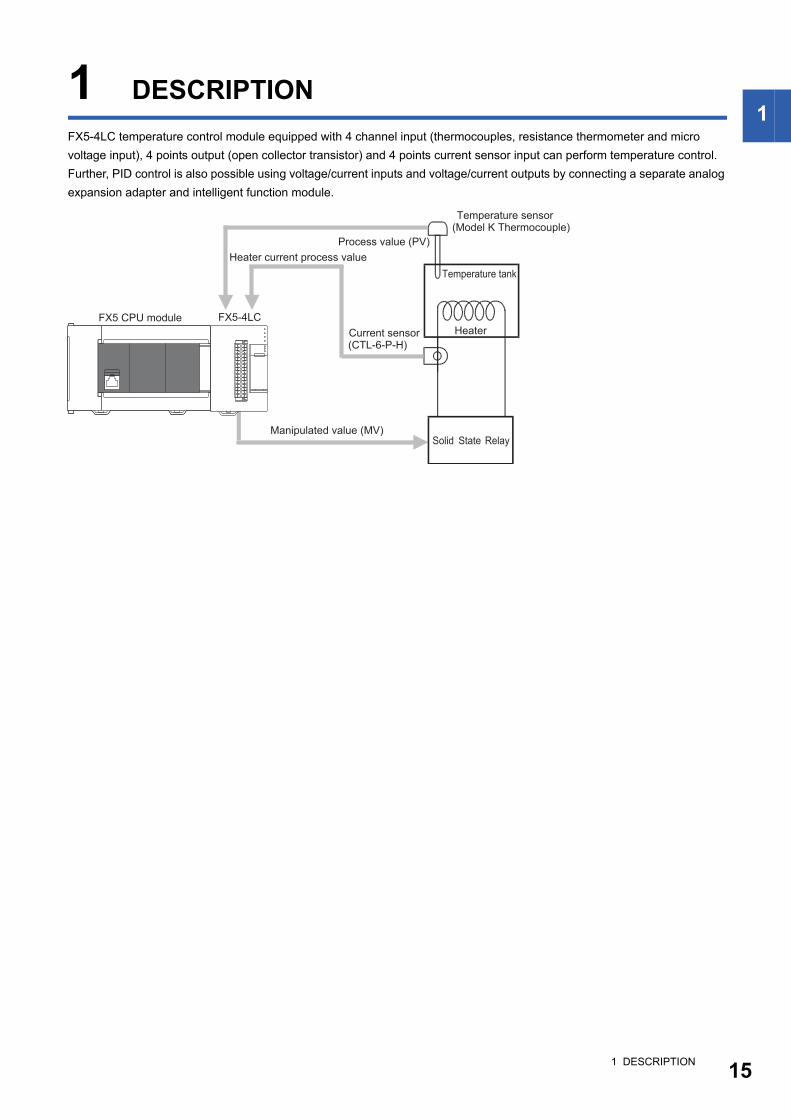
1 DESCRIPTIONFX5-4LC temperature control module equipped with 4 channel input (thermocouples, resistance thermometer and micro
voltage input), 4 points output (open collector transistor) and 4 points current sensor input can perform temperature control.
Further, PID control is also possible using voltage/current inputs and voltage/current outputs by connecting a separate analog
expansion adapter and intelligent function module.
Process value (PV)
Manipulated value (MV)
Temperature sensor(Model K Thermocouple)
Temperature tank
Solid State Relay
Current sensor(CTL-6-P-H)
Heater
Heater current process value
FX5 CPU module FX5-4LC
1 DESCRIPTION 15
16
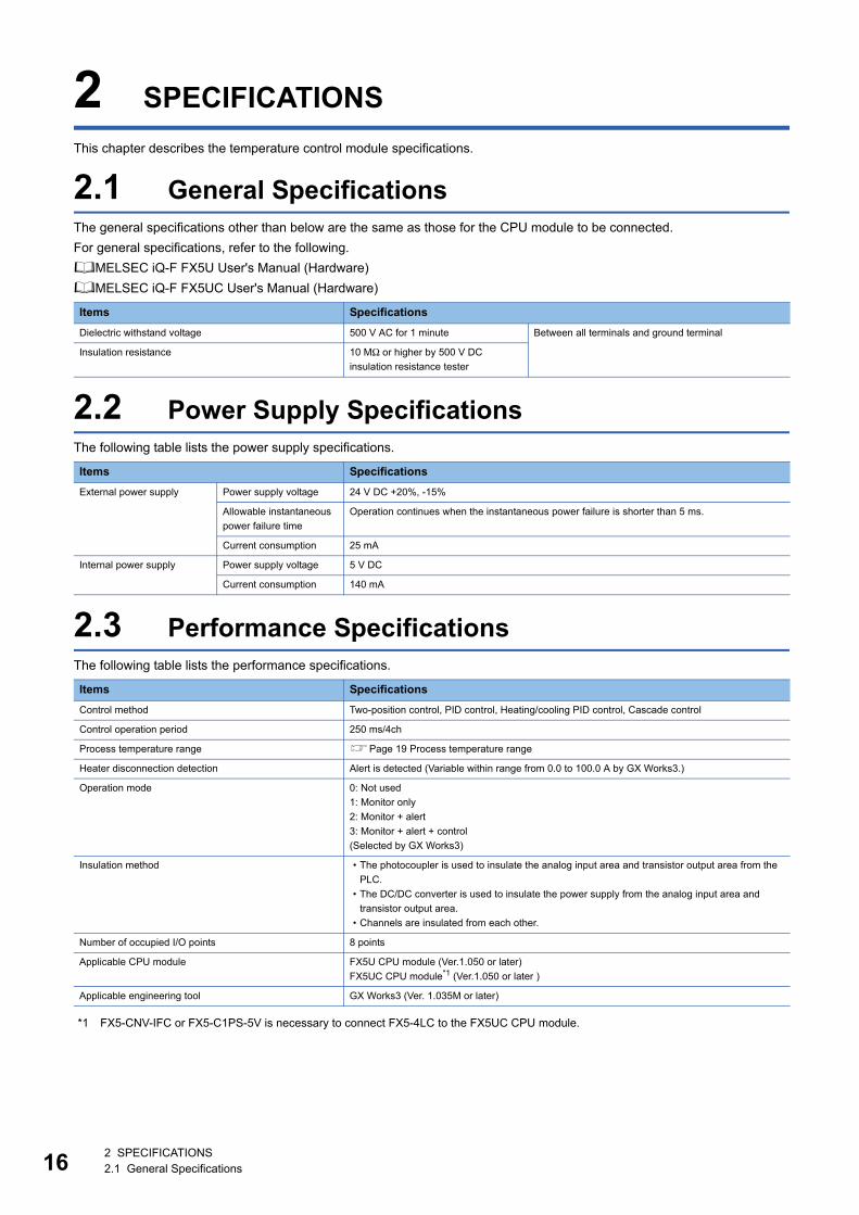
2 SPECIFICATIONS
This chapter describes the temperature control module specifications.
2.1 General SpecificationsThe general specifications other than below are the same as those for the CPU module to be connected.
For general specifications, refer to the following.
MELSEC iQ-F FX5U User's Manual (Hardware)
MELSEC iQ-F FX5UC User's Manual (Hardware)
2.2 Power Supply SpecificationsThe following table lists the power supply specifications.
2.3 Performance SpecificationsThe following table lists the performance specifications.
*1 FX5-CNV-IFC or FX5-C1PS-5V is necessary to connect FX5-4LC to the FX5UC CPU module.
Items Specifications
Dielectric withstand voltage 500 V AC for 1 minute Between all terminals and ground terminal
Insulation resistance 10 MΩ or higher by 500 V DC
insulation resistance tester
Items Specifications
External power supply Power supply voltage 24 V DC +20%, -15%
Allowable instantaneous
power failure time
Operation continues when the instantaneous power failure is shorter than 5 ms.
Current consumption 25 mA
Internal power supply Power supply voltage 5 V DC
Current consumption 140 mA
Items Specifications
Control method Two-position control, PID control, Heating/cooling PID control, Cascade control
Control operation period 250 ms/4ch
Process temperature range Page 19 Process temperature range
Heater disconnection detection Alert is detected (Variable within range from 0.0 to 100.0 A by GX Works3.)
Operation mode 0: Not used
1: Monitor only
2: Monitor + alert
3: Monitor + alert + control
(Selected by GX Works3)
Insulation method • The photocoupler is used to insulate the analog input area and transistor output area from the
PLC.
• The DC/DC converter is used to insulate the power supply from the analog input area and
transistor output area.
• Channels are insulated from each other.
Number of occupied I/O points 8 points
Applicable CPU module FX5U CPU module (Ver.1.050 or later)
FX5UC CPU module*1 (Ver.1.050 or later )
Applicable engineering tool GX Works3 (Ver. 1.035M or later)
2 SPECIFICATIONS2.1 General Specifications
2
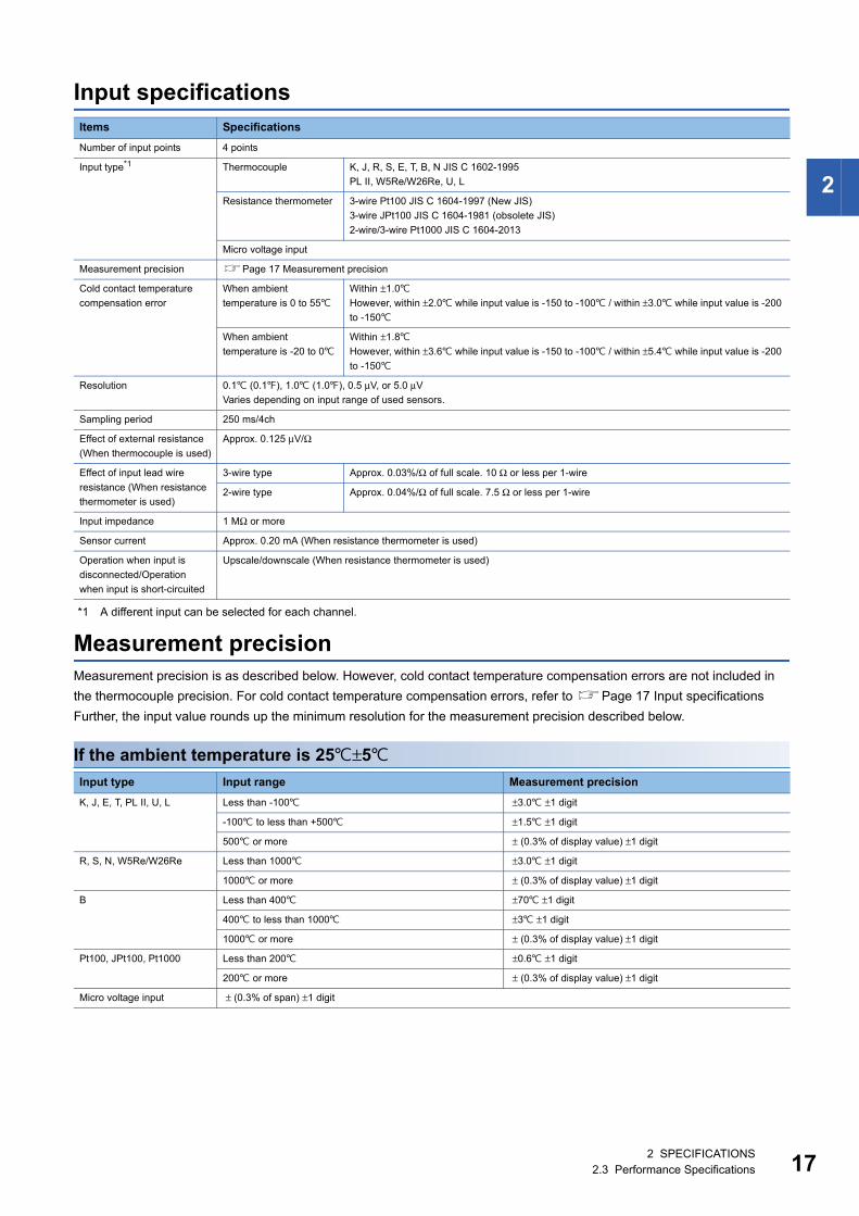
Input specifications
*1 A different input can be selected for each channel.
Measurement precisionMeasurement precision is as described below. However, cold contact temperature compensation errors are not included in
the thermocouple precision. For cold contact temperature compensation errors, refer to Page 17 Input specifications
Further, the input value rounds up the minimum resolution for the measurement precision described below.
If the ambient temperature is 25±5
Items Specifications
Number of input points 4 points
Input type*1 Thermocouple K, J, R, S, E, T, B, N JIS C 1602-1995
PL II, W5Re/W26Re, U, L
Resistance thermometer 3-wire Pt100 JIS C 1604-1997 (New JIS)
3-wire JPt100 JIS C 1604-1981 (obsolete JIS)
2-wire/3-wire Pt1000 JIS C 1604-2013
Micro voltage input
Measurement precision Page 17 Measurement precision
Cold contact temperature
compensation error
When ambient
temperature is 0 to 55
Within ±1.0
However, within ±2.0 while input value is -150 to -100 / within ±3.0 while input value is -200
to -150
When ambient
temperature is -20 to 0
Within ±1.8
However, within ±3.6 while input value is -150 to -100 / within ±5.4 while input value is -200
to -150
Resolution 0.1 (0.1), 1.0 (1.0), 0.5 μV, or 5.0 μV
Varies depending on input range of used sensors.
Sampling period 250 ms/4ch
Effect of external resistance
(When thermocouple is used)
Approx. 0.125 μV/Ω
Effect of input lead wire
resistance (When resistance
thermometer is used)
3-wire type Approx. 0.03%/Ω of full scale. 10 Ω or less per 1-wire
2-wire type Approx. 0.04%/Ω of full scale. 7.5 Ω or less per 1-wire
Input impedance 1 MΩ or more
Sensor current Approx. 0.20 mA (When resistance thermometer is used)
Operation when input is
disconnected/Operation
when input is short-circuited
Upscale/downscale (When resistance thermometer is used)
Input type Input range Measurement precision
K, J, E, T, PL II, U, L Less than -100 ±3.0 ±1 digit
-100 to less than +500 ±1.5 ±1 digit
500 or more ± (0.3% of display value) ±1 digit
R, S, N, W5Re/W26Re Less than 1000 ±3.0 ±1 digit
1000 or more ± (0.3% of display value) ±1 digit
B Less than 400 ±70 ±1 digit
400 to less than 1000 ±3 ±1 digit
1000 or more ± (0.3% of display value) ±1 digit
Pt100, JPt100, Pt1000 Less than 200 ±0.6 ±1 digit
200 or more ± (0.3% of display value) ±1 digit
Micro voltage input ± (0.3% of span) ±1 digit
2 SPECIFICATIONS2.3 Performance Specifications 17
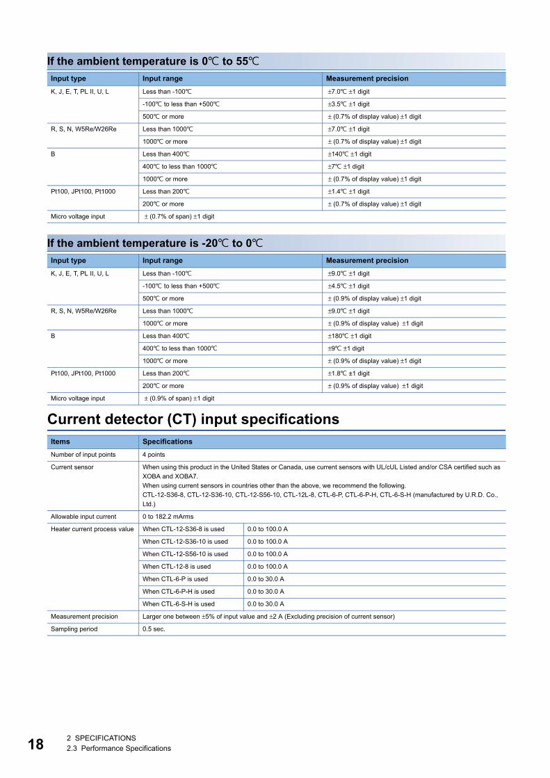
18
If the ambient temperature is 0 to 55
If the ambient temperature is -20 to 0
Current detector (CT) input specifications
Input type Input range Measurement precision
K, J, E, T, PL II, U, L Less than -100 ±7.0 ±1 digit
-100 to less than +500 ±3.5 ±1 digit
500 or more ± (0.7% of display value) ±1 digit
R, S, N, W5Re/W26Re Less than 1000 ±7.0 ±1 digit
1000 or more ± (0.7% of display value) ±1 digit
B Less than 400 ±140 ±1 digit
400 to less than 1000 ±7 ±1 digit
1000 or more ± (0.7% of display value) ±1 digit
Pt100, JPt100, Pt1000 Less than 200 ±1.4 ±1 digit
200 or more ± (0.7% of display value) ±1 digit
Micro voltage input ± (0.7% of span) ±1 digit
Input type Input range Measurement precision
K, J, E, T, PL II, U, L Less than -100 ±9.0 ±1 digit
-100 to less than +500 ±4.5 ±1 digit
500 or more ± (0.9% of display value) ±1 digit
R, S, N, W5Re/W26Re Less than 1000 ±9.0 ±1 digit
1000 or more ± (0.9% of display value) ±1 digit
B Less than 400 ±180 ±1 digit
400 to less than 1000 ±9 ±1 digit
1000 or more ± (0.9% of display value) ±1 digit
Pt100, JPt100, Pt1000 Less than 200 ±1.8 ±1 digit
200 or more ± (0.9% of display value) ±1 digit
Micro voltage input ± (0.9% of span) ±1 digit
Items Specifications
Number of input points 4 points
Current sensor When using this product in the United States or Canada, use current sensors with UL/cUL Listed and/or CSA certified such as
XOBA and XOBA7.
When using current sensors in countries other than the above, we recommend the following.
CTL-12-S36-8, CTL-12-S36-10, CTL-12-S56-10, CTL-12L-8, CTL-6-P, CTL-6-P-H, CTL-6-S-H (manufactured by U.R.D. Co.,
Ltd.)
Allowable input current 0 to 182.2 mArms
Heater current process value When CTL-12-S36-8 is used 0.0 to 100.0 A
When CTL-12-S36-10 is used 0.0 to 100.0 A
When CTL-12-S56-10 is used 0.0 to 100.0 A
When CTL-12-8 is used 0.0 to 100.0 A
When CTL-6-P is used 0.0 to 30.0 A
When CTL-6-P-H is used 0.0 to 30.0 A
When CTL-6-S-H is used 0.0 to 30.0 A
Measurement precision Larger one between ±5% of input value and ±2 A (Excluding precision of current sensor)
Sampling period 0.5 sec.
2 SPECIFICATIONS2.3 Performance Specifications
2
Process valuesTo stabilize the measurement precision, warm-up (supply power) the system for 30 minutes or more after power-on.
Process temperature range
Output specifications
Items Specifications
K -200 to +1300 (-100 to +2400)
J -200 to +1200 (-100 to +2100)
T -200 to +400 (-300 to +700)
S 0 to 1700 (0 to 3200)
R 0 to 1700 (0 to 3200)
E -200 to +1000 (0 to 1800)
B 0 to 1800 (0 to 3000)
N 0 to 1300 (0 to 2300)
PL 0 to 1200 (0 to 2300)
W5Re/W26Re 0 to 2300 (0 to 3000)
U -200 to +600 (-300 to +700)
L 0 to 900 (0 to 1600)
Micro voltage input DC0 to 10 mV, DC0 to 100 mV
Pt100 (3-wire type) -200 to +600 (-300 to +1100)
JPt100 (3-wire type) -200 to +500 (-300 to +900)
Pt1000 (2-wire type/3-wire
type)
-200.0 to +650.0 (-328 to +1184)
Items Specifications
Number of output points 4 points
Output method NPN open collector transistor output
Rated load voltage 5 to 24 V DC
Maximum load voltage 30 V DC or less
Maximum load current 100 mA
Leak current in OFF status 0.1 mA or less
ON voltage 1.5 V (When maximum load current)
Control output cycle 0.5 to 100.0 sec.
2 SPECIFICATIONS2.3 Performance Specifications 19
20
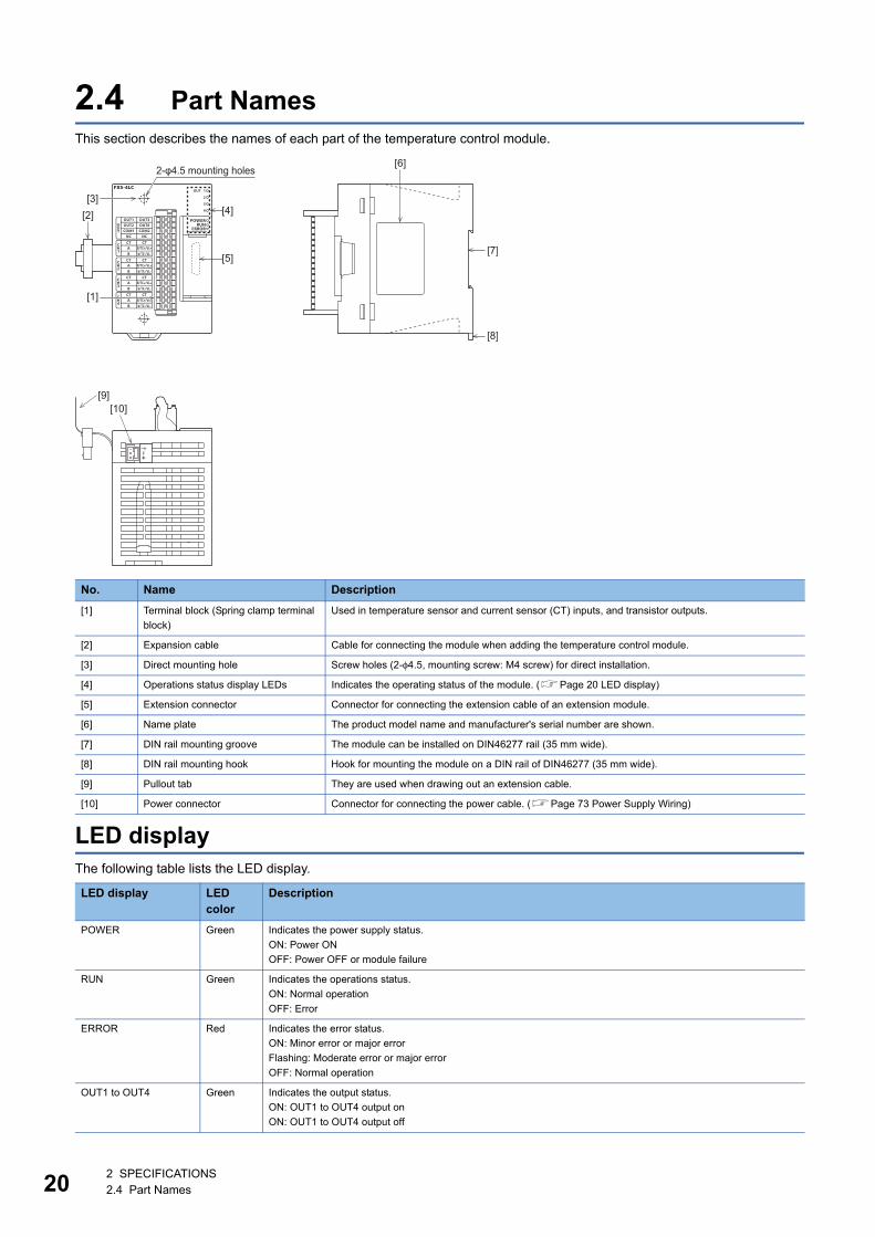
2.4 Part NamesThis section describes the names of each part of the temperature control module.
LED displayThe following table lists the LED display.
No. Name Description
[1] Terminal block (Spring clamp terminal
block)
Used in temperature sensor and current sensor (CT) inputs, and transistor outputs.
[2] Expansion cable Cable for connecting the module when adding the temperature control module.
[3] Direct mounting hole Screw holes (2-φ4.5, mounting screw: M4 screw) for direct installation.
[4] Operations status display LEDs Indicates the operating status of the module. (Page 20 LED display)
[5] Extension connector Connector for connecting the extension cable of an extension module.
[6] Name plate The product model name and manufacturer's serial number are shown.
[7] DIN rail mounting groove The module can be installed on DIN46277 rail (35 mm wide).
[8] DIN rail mounting hook Hook for mounting the module on a DIN rail of DIN46277 (35 mm wide).
[9] Pullout tab They are used when drawing out an extension cable.
[10] Power connector Connector for connecting the power cable. (Page 73 Power Supply Wiring)
LED display LED color
Description
POWER Green Indicates the power supply status.
ON: Power ON
OFF: Power OFF or module failure
RUN Green Indicates the operations status.
ON: Normal operation
OFF: Error
ERROR Red Indicates the error status.
ON: Minor error or major error
Flashing: Moderate error or major error
OFF: Normal operation
OUT1 to OUT4 Green Indicates the output status.
ON: OUT1 to OUT4 output on
ON: OUT1 to OUT4 output off
[3]
[1]
[2]
[7]
[6]
[8]
[4]
2-φ4.5 mounting holes
[5]
[10][9]
2 SPECIFICATIONS2.4 Part Names
3
3 PROCEDURES BEFORE OPERATION
This chapter describes the procedures before operation.
1. Checking the temperature control module specifications
Check the temperature control module specifications. (Page 16 SPECIFICATIONS)
2. Mounting the temperature control module
Mount the temperature control module to the FX5 CPU module. For details, refer to the following.
MELSEC iQ-F FX5U User's Manual (Hardware)
MELSEC iQ-F FX5UC User's Manual (Hardware)
3. Wiring
Wire the external devices to the temperature control module.
4. Adding modules
Add temperature controllers to the module configuration using GX Works3.
When adding a temperature control module, FX3 allocation mode is usable if a module with the suffix
"(FX3)"after its name is selected.
• FX5-4LC: Normal mode
• FX5-4LC (FX3): FX3 allocation mode
5. Parameter settings
Set the temperature control module parameters using GX Works3.
6. Implementing auto tuning
If implementing auto tuning, set PID using the auto tuning function.
7. Programming
Create the program.
8. Warm-up operations
Implement warm-up for approx. 30 mins. before starting operations.
3 PROCEDURES BEFORE OPERATION 21
22
4 FUNCTION
This chapter describes the function details of the temperature control module.
For details on the buffer memory, refer to the following.
Page 117 Details of buffer memory addresses
This chapter describes the buffer memory for CH1.
For details on the buffer memory addresses for CH2 or later, refer to the following.
Page 99 List of buffer memory addresses
4.1 Functions listThe following table lists the temperature control module functions.
Items Description Usability Reference
Standard PID control
Heating/cooling PID control
Control mode selection function Use this function to select the control mode from among
those described below.
• Standard PID control
• Heating/cooling PID control
Page 24
Control method Two-position control Control methods can be achieved by setting a
proportional band (P), integral time (I), and derivative
time (D).
Page 26
P control
PI control
PD control
PID control
Manual control A manipulated value (MV) can be set manually by users
without being automatically calculated by the PID control.
Page 30
Balance bumpless function This function prevents sudden outputs change during
AUTO↔MAN mode switching.
Page 31
RFB limiter function When the deviation (E) continues for a long period of
time, this function prevents the PID operation results
(manipulated value (MV)) calculated by integral actions
from exceeding the effective range of the manipulated
value (MV).
Page 31
Simple two-degree-of-freedom In addition to the PID control, this function selects a
suitable response speed for the set value (SV) change
from three levels to simply achieve the two-degree-of-
freedom PID control.
Page 32
Normal operation/reverse operation
selection function
Select whether or not to implement a PID operation with
a normal operation or a reverse operation.
Page 32
Proportional band setting function This function can set the proportional bands (P) for
heating and cooling individually.
Page 33
Overlap/dead band function The temperature where the cooling control output starts
can be shifted using this function and, consequently,
whether control stability is prioritized or energy saving is
prioritized can be selected.
Page 34
Cooling method setting function During auto tuning, an auto tuning operational expression
is automatically selected depending on a selected
cooling method and an operation starts.
Page 35
Auto tuning function The temperature control module automatically sets the
best PID constants.
Page 36
AT bias function This function changes the AT point by applying bias to
the set value (SV) during auto tuning.
Page 40
4 FUNCTION4.1 Functions list
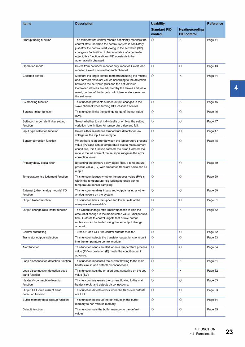
4
Startup tuning function The temperature control module constantly monitors the
control state, so when the control system is oscillatory
just after the control start, owing to the set value (SV)
change or fluctuation of characteristics of a controlled
object, this function allows PID constants to be
automatically changed.
Page 41
Operation mode Select from not used, monitor only, monitor + alert, and
monitor + alert + control for each channel.
Page 43
Cascade control Monitors the target control temperature using the master,
and corrects slave set values according to the deviation
between the set value (SV) and the actual value.
Controlled devices are adjusted by the slaves and, as a
result, control of the target control temperature reaches
the set value.
Page 44
SV tracking function This function prevents sudden output changes in the
slave channel when turning OFF cascade control.
Page 46
Settings limiter function This function limits the settings range of the set value
(SV).
Page 46
Setting change rate limiter setting
function
Select whether to set individually or en bloc the setting
variation rate limiters for temperature rise and fall.
Page 47
Input type selection function Select either resistance temperature detector or low
voltage as the input sensor type.
Page 47
Sensor correction function When there is an error between the temperature process
value (PV) and actual temperature due to measurement
conditions, this function corrects the error. Corrects the
ratio to the full scale of the set input range as the error
correction value.
Page 48
Primary delay digital filter By setting the primary delay digital filter, a temperature
process value (PV) with smoothed transient noise can be
output.
Page 49
Temperature rise judgment function This function judges whether the process value (PV) is
within the temperature rise judgment range during
temperature sensor sampling.
Page 50
External (other analog module) I/O
function
This function enables inputs and outputs using another
analog module on the system.
Page 50
Output limiter function This function limits the upper and lower limits of the
manipulated value (MV).
Page 51
Output change ratio limiter function The Output change ratio limiter functions to limit the
amount of change in the manipulated value (MV) per unit
time. Outputs to control targets that dislike output
mutations can be limited using the set output change
amount.
Page 52
Control output flag Turns ON and OFF the control outputs monitor. Page 52
Transistor outputs selection This function selects the transistor output functions built
into the temperature control module.
Page 53
Alert function This function sends an alert when a temperature process
value (PV) or deviation (E) meets the condition set in
advance.
Page 54
Loop disconnection detection function This function measures the current flowing to the main
heater circuit, and detects disconnections.
Page 61
Loop disconnection detection dead
band function
This function sets the on-alert area centering on the set
value (SV).
Page 62
Heater disconnection detection
function
This function measures the current flowing to the main
heater circuit, and detects disconnections.
Page 63
Output OFF-time current error
detection function
This function detects errors when the transistor outputs
are OFF.
Page 63
Buffer memory data backup function This function backs up the set values in the buffer
memory to non-volatile memory.
Page 64
Default function This function sets the buffer memory to the default
values.
Page 65
Items Description Usability Reference
Standard PID control
Heating/cooling PID control
4 FUNCTION4.1 Functions list 23
24
4.2 Control Mode Selection FunctionThis function selects the I/Os (external or internal) to be used as the control type (standard PID control for heating and cooling
PID control) for each control group.
The control groups are divided as described below.
• Control group 1: CH1 and CH2
• Control group 2: CH3 and CH4
Standard PID control, heating and cooling PID controlThere are two types of control modes in the temperature control module: Standard PID control and heating-cooling PID
control.
■Standard PID controlThis control method attempts to acquire stable control results by setting the constants for P (proportional band) I (integral
time) and D (derivative time).
"Response to noise" worsens for this PID control if the PID constants are set to improve "Response to settings". Further,
"Response to settings" worsens if the PID constants are set to improve "Response to noise".
The temperature control module can be used to select "Fast", "Normal", and "Slow" using the control response parameters for
the shape of the "Response to settings" with the PID constants to improve "Response to noise" unchanged.
■Heating/cooling PID controlHeating and cooling PID controls are the control methods that operate the outputs for both the heating and cooling control
systems.
In heating, the manipulated value (MV) operation decreases (reverse operation) according to increases in the process value
(PV), and in cooling, the manipulated value (MV) operation increased (normal operation) according to increases in the
process value (PV).
Set cooling and heating PID constants individually for proportional band (P) cooling and heating. Integral time (I) and
derivative time (D) are common set values for both heating and cooling.
Consequently, the temperature control module implements calculations using the four PID constants of heating proportional
band, cooling proportional band, integral time, and derivative time.
Further, it is possible to establish dead bands, and implement overlap and outputs, using the heating and cooling control
switching points.
Error history function This function stores a maximum of 16 errors and alarms
that occurred in the temperature control module to buffer
memory as a history.
Page 65
FX3 allocation mode function The temperature control module buffer memory
addresses can be arranged in the same way as for
FX3U-4LC.
Page 68
Items Description Usability Reference
Standard PID control
Heating/cooling PID control
4 FUNCTION4.2 Control Mode Selection Function
4
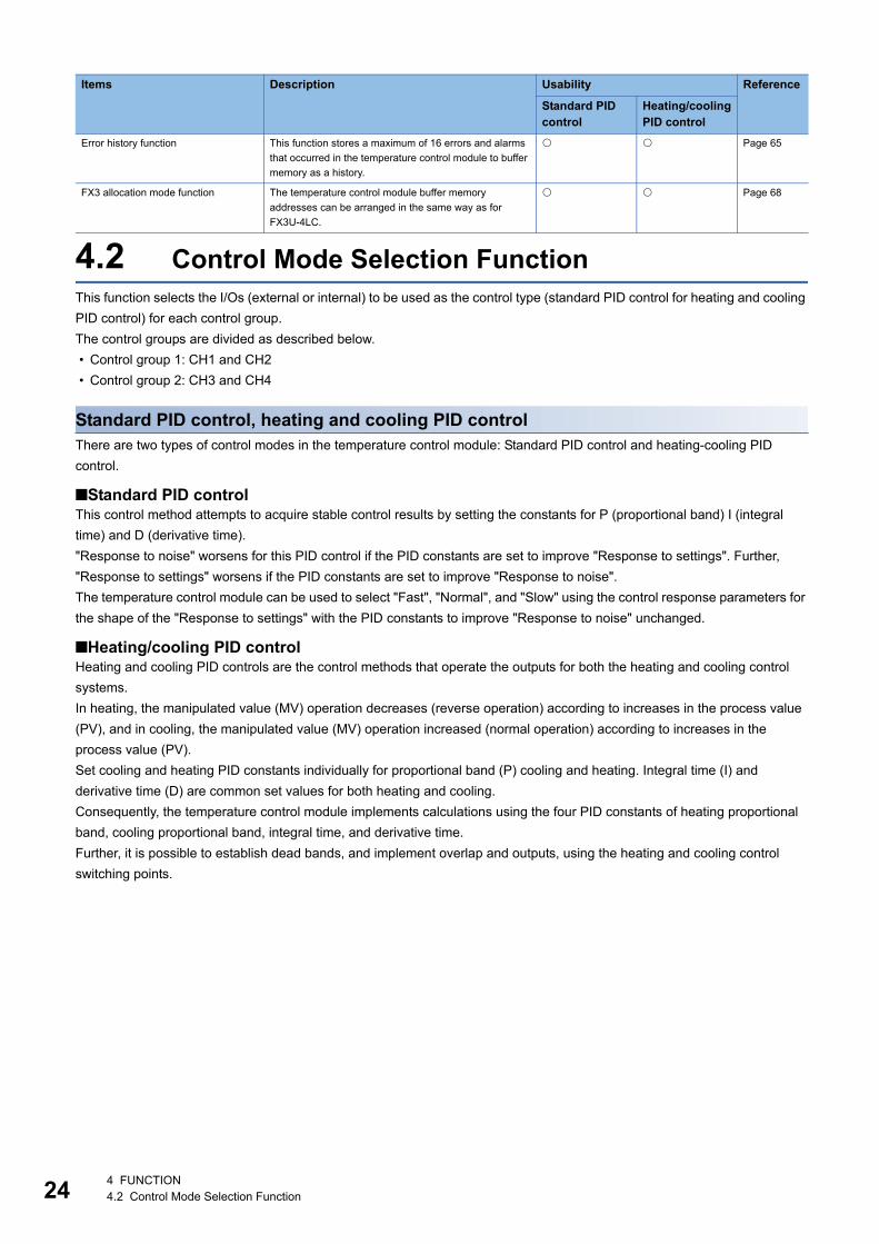
Selectable control modesA control mode can be selected from the modes described below. Select a control mode in "Control mode selection" of "Base
Setting".
If Internal is selected in either inputs or outputs, control is implemented using the I/O built into the temperature control module.
If External is selected in either inputs or outputs, control is implemented using another analog module connected to the CPU
module.
■If external inputs are selectedIf external inputs are selected, the parameters are as described below.
• Input range setting
The internal span is from "external input range upper limit" to "external input range lower limit".
The input range is from "external input range lower limit" to "external input range upper limit".
• Settings limiter
The settings range for the upper limit setting limiter is from "lower limit setting limiter value +1" to "External input range upper
limit".
The settings range for the lower limit setting limiter is from "external input range lower limit" to "upper limit setting limiter -1".
• Set value settings
The set value settings are from "lower limit setting limiter" to "upper limit setting limiter".
• Input errors
If a value at or greater than "external input range upper limit +5%/Input span" is set in the external input value, an (upper limit)
input error occurs, and an event (Un\G429, b0) turns ON.
If a value at or less than "external input range lower limit -5%/Input span" is set in the external input value, a (lower limit) input
error occurs, and an event (Un\G429, b1) turns ON.
■If external outputs are selectedIf external outputs are selected, the values that scale the control output value (from the external output range lower limit to the
external output range upper limit) are written to the manipulated value (MV) for external (other analog module) outputs,
Manipulated value for heating (MVh) for external (other analog module) outputs, and Manipulated value for cooling (MVc) for
external (other analog module) outputs, regardless of the control mode switching settings.
Control mode Control types Input Output
0 Standard PID control Internal Internal
1 Standard PID control External Internal
2 Standard PID control Internal External
3 Standard PID control External External
4 Heating/cooling PID control Internal Internal
5 Heating/cooling PID control External Internal
6 Heating/cooling PID control Internal External
7 Heating/cooling PID control External External
4 FUNCTION4.2 Control Mode Selection Function 25
26
4.3 Control MethodThe following control methods can be achieved by setting a proportional band (P), integral time (I), and derivative time (D).
• Two-position control
• P control
• PI control
• PD control
• PID control
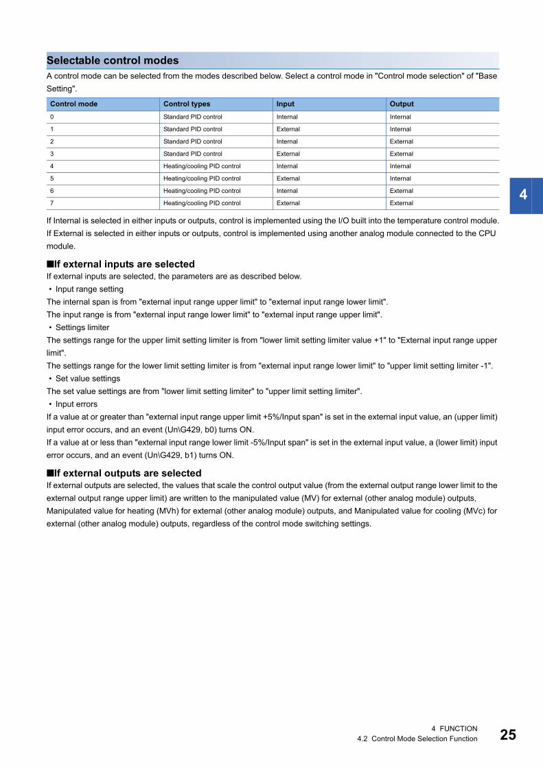
Two-position controlTwo-position control is a control method that uses the 0% manipulated value (MV) and 100% manipulated value (MV).
Turning ON and OFF the manipulated value (MV) repeatedly makes the temperature process value come close to the set
value (SV), and the temperature is kept constant.
By the setting in "Adjustment sensitivity (dead band) setting" of "Application Setting", the chattering of
transistor outputs under two-position control can be prevented. Set the set value (SV).
■Standard PID controlThe module operates as described below outside the setting range of "Adjustment sensitivity (dead band) setting" in
"Application Setting".
Condition Transistor output status
The temperature process value (PV) is below the lower limit of the adjustment
sensitivity (dead band)
ON
The temperature process value (PV) is above the upper limit of the adjustment
sensitivity (dead band)
OFF
Temperature process value (PV)
Time
Adjustment sensitivity(dead band)
Manipulated value (MV)
Set value (SV)
OFF
ON
4 FUNCTION4.3 Control Method
4
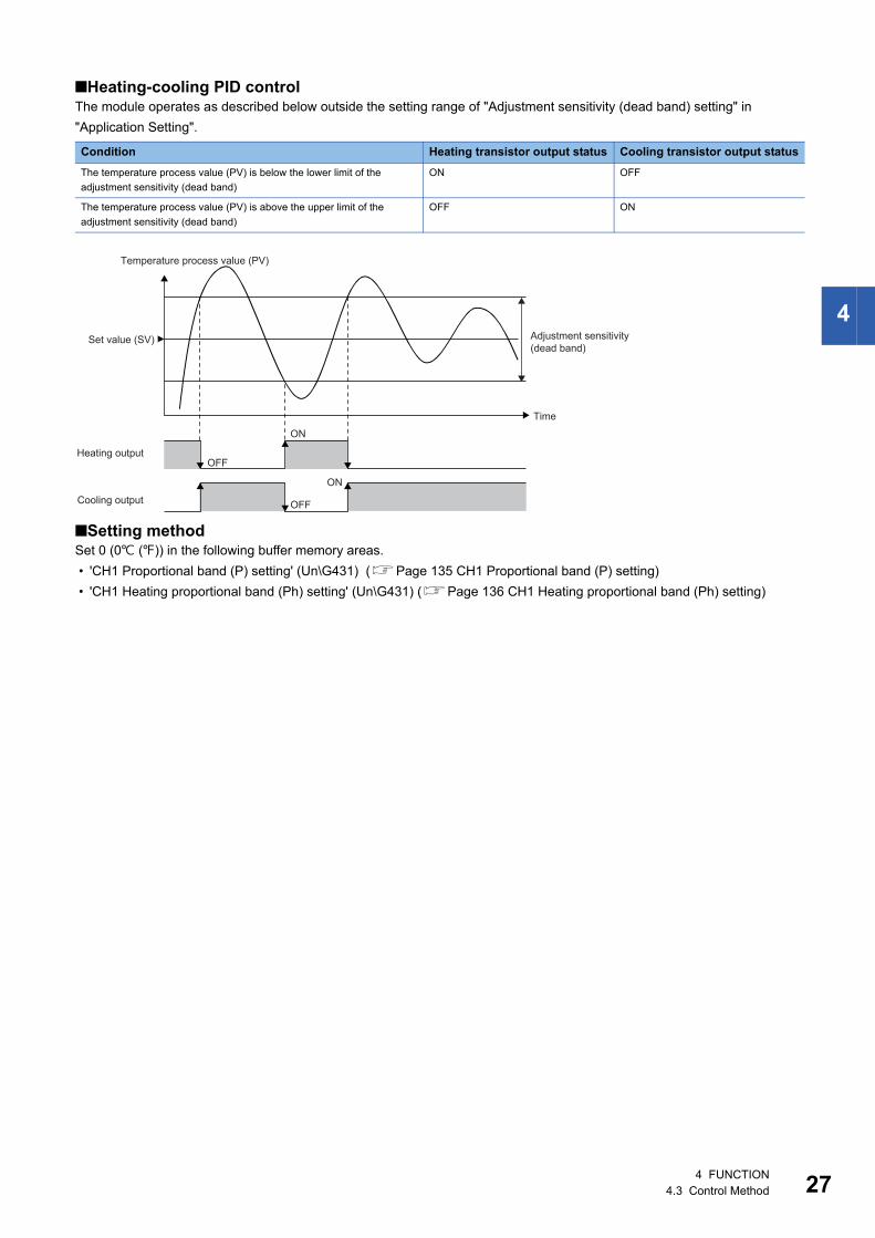
■Heating-cooling PID controlThe module operates as described below outside the setting range of "Adjustment sensitivity (dead band) setting" in
"Application Setting".
■Setting methodSet 0 (0 ()) in the following buffer memory areas.
• 'CH1 Proportional band (P) setting' (Un\G431) (Page 135 CH1 Proportional band (P) setting)
• 'CH1 Heating proportional band (Ph) setting' (Un\G431) (Page 136 CH1 Heating proportional band (Ph) setting)
Condition Heating transistor output status Cooling transistor output status
The temperature process value (PV) is below the lower limit of the
adjustment sensitivity (dead band)
ON OFF
The temperature process value (PV) is above the upper limit of the
adjustment sensitivity (dead band)
OFF ON
OFF
ON
ON
OFF
Temperature process value (PV)
Time
Adjustment sensitivity (dead band)
Set value (SV)
Heating output
Cooling output
4 FUNCTION4.3 Control Method 27
28
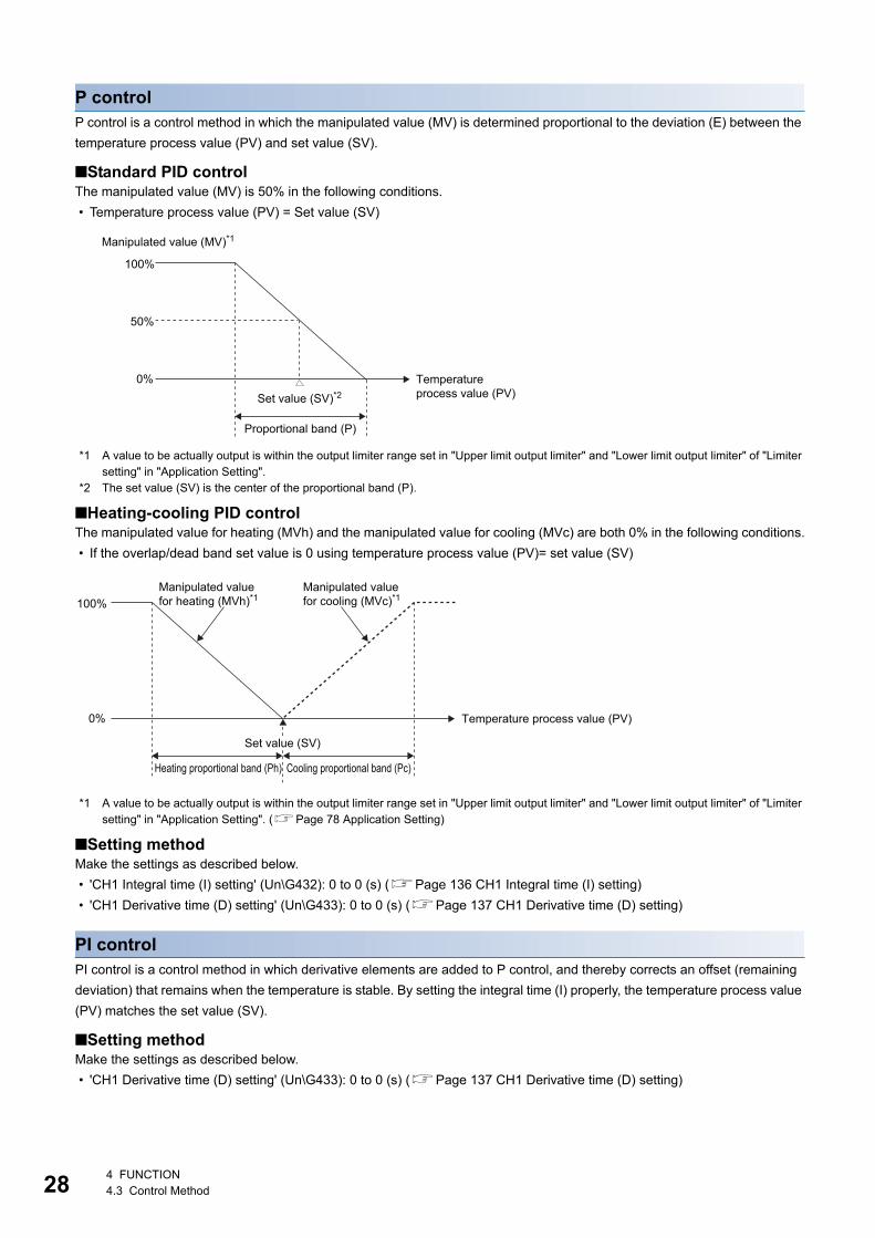
P controlP control is a control method in which the manipulated value (MV) is determined proportional to the deviation (E) between the
temperature process value (PV) and set value (SV).
■Standard PID controlThe manipulated value (MV) is 50% in the following conditions.
• Temperature process value (PV) = Set value (SV)
*1 A value to be actually output is within the output limiter range set in "Upper limit output limiter" and "Lower limit output limiter" of "Limiter setting" in "Application Setting".
*2 The set value (SV) is the center of the proportional band (P).
■Heating-cooling PID controlThe manipulated value for heating (MVh) and the manipulated value for cooling (MVc) are both 0% in the following conditions.
• If the overlap/dead band set value is 0 using temperature process value (PV)= set value (SV)
*1 A value to be actually output is within the output limiter range set in "Upper limit output limiter" and "Lower limit output limiter" of "Limiter setting" in "Application Setting". (Page 78 Application Setting)
■Setting methodMake the settings as described below.
• 'CH1 Integral time (I) setting' (Un\G432): 0 to 0 (s) (Page 136 CH1 Integral time (I) setting)
• 'CH1 Derivative time (D) setting' (Un\G433): 0 to 0 (s) (Page 137 CH1 Derivative time (D) setting)
PI controlPI control is a control method in which derivative elements are added to P control, and thereby corrects an offset (remaining
deviation) that remains when the temperature is stable. By setting the integral time (I) properly, the temperature process value
(PV) matches the set value (SV).
■Setting methodMake the settings as described below.
• 'CH1 Derivative time (D) setting' (Un\G433): 0 to 0 (s) (Page 137 CH1 Derivative time (D) setting)
Manipulated value (MV)*1
100%
0%Set value (SV)*2
Proportional band (P)
Temperature process value (PV)
50%
100%
0%
Set value (SV)
Heating proportional band (Ph) Cooling proportional band (Pc)
Temperature process value (PV)
Manipulated value for heating (MVh)*1
Manipulated value for cooling (MVc)*1
4 FUNCTION4.3 Control Method
4
PD controlPD control is a control method in which the derivative time (D) is set in addition to P control. The control mechanism is the
same as P control.
■Setting methodMake the settings as described below.
• 'CH1 Integral time (I) setting' (Un\G432): 0 to 0 (s) (Page 136 CH1 Integral time (I) setting)
PID controlPID control is a control method in which derivative elements are added to PI control, and thereby the temperature shifts to a
stable status in a short period of time even when a drastic change has occurred. By setting the derivative time (D) properly,
the controlled object shifts to a stable status in a short period of time.
■Settings method (If using standard PID control)Make the settings as described below.
• 'CH1 Proportional band (P) setting' (Un\G431): Any value ( Page 135 CH1 Proportional band (P) setting)
• 'CH1 Integral time (I) setting' (Un\G432): Any value ( Page 136 CH1 Integral time (I) setting)
• 'CH1 Derivative time (D) setting' (Un\G433): Any value ( Page 137 CH1 Derivative time (D) setting)
■Settings method (If using heating-cooling PID control)Make the settings as described below.
• 'CH1 Heating proportional band (Ph) setting' (Un\G431): Any value ( Page 136 CH1 Heating proportional band (Ph)
setting)
• 'CH1 Cooling proportional band (Pc) setting' (Un\G439): Any value ( Page 140 CH1 Cooling proportional band (Pc)
setting)
• 'CH1 Integral time (I) setting' (Un\G432): Any value (Page 136 CH1 Integral time (I) setting)
• 'CH1 Derivative time (D) setting' (Un\G433): Any value (Page 137 CH1 Derivative time (D) setting)
Parameters related to control methodsThe following table shows the parameters related to each control method.
Parameter Setting range
Two-position control
P control PD control PI control PID control
Input range setting • Thermocouple: 0 to 35
• Platinum resistance thermometer: 36 to 45
• Micro voltage input: 46 to 47
Set value (SV) setting Set a value within the temperature measuring range of the set input range.
Adjustment sensitivity
(dead band) setting
1 to 100 (0.1 to 10.0%) The set value is ignored.
Upper limit output
limiter, lower limit
output limiter (standard
PID control only)
The set value is
ignored.
-50 to 1050 (-5.0 to 105.0%)
Upper limit output
limiter, cooling upper
limit output limiter
(heating-cooling PID
control only)
The set value is
ignored.
0 to 1050 (0.0 to 105.0%)
Output change ratio
limiter
The set value is
ignored.
1 to 1000 (1 to 100.0%/s)
Control output cycle
setting
The set value is
ignored.
• Settings range: 5 to 1000 (0.5 to 100.0 s)
• Default value: 300 (30.0 s)
Cooling control output
cycle setting (heating-
cooling PID control
only)
The set value is
ignored.
• Settings range: 5 to 1000 (0.5 to 100.0 s)
• Default value: 300 (30.0 s)
Overlap/dead band
setting
-100 to 100 (-10.0 to 10.0%)
4 FUNCTION4.3 Control Method 29
30
Buffer memory areas related to control methodsThe following table shows the buffer memory areas related to each control method.
The temperature control module automatically sets optimum PID constants when the following functions are
used.
• Auto Tuning Function (Page 36 Auto Tuning Function)
• Startup tuning function (Page 41 Startup Tuning Function)
4.4 Manual ControlA manipulated value (MV) can be set manually by users without being automatically calculated using the PID control.
Setting methodConfigure the settings as described below.
1. Set 'CH1 AUTO/MAN mode shift' (Un\G518) to Manual (MAN) (1). (Page 149 CH1 AUTO/MAN mode shift)
2. Set the manipulated value (MV) in 'CH1 Manual output setting' (Un\G519). (Page 150 CH1 Manual output setting)
Setting rangeThe settings range is as described below.
• -50 to 1050 (-5.0 to 105.0%)
Buffer memory name
Buffer memory address
Setting range
Two-position control
P control PD control P control PID control
CH1 Cooling
proportional band (P)
setting, CH1 Heating
proportional band (Ph)
setting (If using normal
mode)
431 Fix the setting to 0. 0 to 10000 (0.0 to 1000.0% span)
CH1 Cooling
proportional band (Pc)
setting (If using normal
mode)
439
CH1 Integral time (I)
setting (If using normal
mode)
432 The set value is
ignored.
Fix the setting to 0. 1 to 3600(s)
CH1 Differential time
(D) setting (If using
normal mode)
433 The set value is
ignored.
Fix the setting to 0. 1 to 3600(s) The set value is
ignored.
1 to 3600(s)
4 FUNCTION4.4 Manual Control
4
4.5 Balance Bumpless FunctionPrevents overshoot due to sudden changes in the manipulated value (MV) when switching from AUTO mode to MAN mode
(or from MAN mode to AUTO mode).
The balance bumpless from MAN mode to AUTO mode function is enabled only during PID control or PI control mode.
This function automatically operates during switching. No particular settings are required.
4.6 RFB Limiter FunctionThe RFB (reset feedback) function operates when deviation (E) continues for a long period of time.
When the deviation (E) continues for a long period of time, this function prevents the PID operation results (manipulated value
(MV)) calculated by integral actions from exceeding the effective range of the manipulated value (MV).
This function automatically operates when the PID control is implemented. No particular settings are required.
When a PID operation result is larger than the upper limit output limiter value, the temperature control module
operates as described below.
• The RFB function levels the manipulated value (MV) to the upper limit output limiter value by feeding back
an excess value to the integral value.
When a PID operation result is smaller than the lower limit output limiter value, the temperature control
module operates as described below.
• The RFB function levels the manipulated value (MV) to the lower limit output limiter value by feeding back a
required value to the integral value.
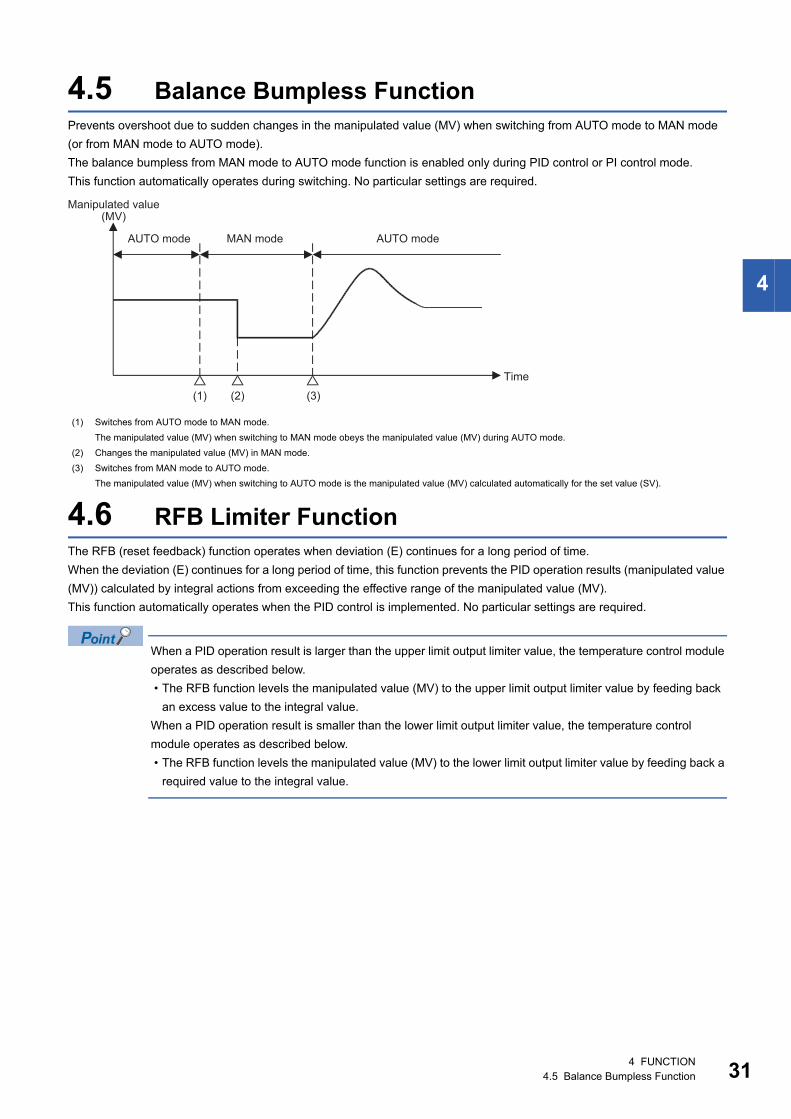
(1) Switches from AUTO mode to MAN mode.
The manipulated value (MV) when switching to MAN mode obeys the manipulated value (MV) during AUTO mode.
(2) Changes the manipulated value (MV) in MAN mode.
(3) Switches from MAN mode to AUTO mode.
The manipulated value (MV) when switching to AUTO mode is the manipulated value (MV) calculated automatically for the set value (SV).
Manipulated value(MV)
AUTO mode MAN mode AUTO mode
Time
(1) (3)(2)
4 FUNCTION4.5 Balance Bumpless Function 31
32
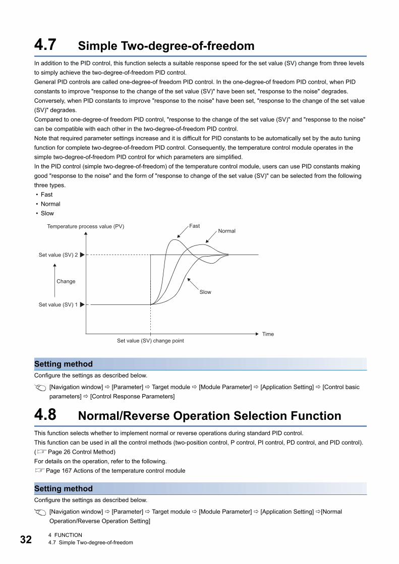
4.7 Simple Two-degree-of-freedomIn addition to the PID control, this function selects a suitable response speed for the set value (SV) change from three levels
to simply achieve the two-degree-of-freedom PID control.
General PID controls are called one-degree-of freedom PID control. In the one-degree-of freedom PID control, when PID
constants to improve "response to the change of the set value (SV)" have been set, "response to the noise" degrades.
Conversely, when PID constants to improve "response to the noise" have been set, "response to the change of the set value
(SV)" degrades.
Compared to one-degree-of freedom PID control, "response to the change of the set value (SV)" and "response to the noise"
can be compatible with each other in the two-degree-of-freedom PID control.
Note that required parameter settings increase and it is difficult for PID constants to be automatically set by the auto tuning
function for complete two-degree-of-freedom PID control. Consequently, the temperature control module operates in the
simple two-degree-of-freedom PID control for which parameters are simplified.
In the PID control (simple two-degree-of-freedom) of the temperature control module, users can use PID constants making
good "response to the noise" and the form of "response to change of the set value (SV)" can be selected from the following
three types.
• Fast
• Normal
• Slow
Setting methodConfigure the settings as described below.
[Navigation window] [Parameter] Target module [Module Parameter] [Application Setting] [Control basic
parameters] [Control Response Parameters]
4.8 Normal/Reverse Operation Selection FunctionThis function selects whether to implement normal or reverse operations during standard PID control.
This function can be used in all the control methods (two-position control, P control, PI control, PD control, and PID control).
(Page 26 Control Method)
For details on the operation, refer to the following.
Page 167 Actions of the temperature control module
Setting methodConfigure the settings as described below.
[Navigation window] [Parameter] Target module [Module Parameter] [Application Setting] [Normal
Operation/Reverse Operation Setting]
Time
Temperature process value (PV)
Set value (SV) 2
Set value (SV) 1
Change
Set value (SV) change point
FastNormal
Slow
4 FUNCTION4.7 Simple Two-degree-of-freedom
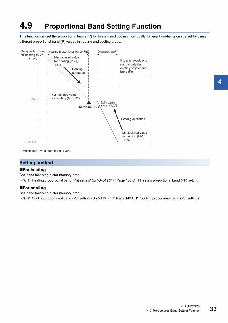
4
4.9 Proportional Band Setting FunctionThis function can set the proportional bands (P) for heating and cooling individually. Different gradients can be set by using
different proportional band (P) values in heating and cooling areas.
Setting method
■For heatingSet in the following buffer memory area.
• 'CH1 Heating proportional band (Ph) setting' (Un\G431) (Page 136 CH1 Heating proportional band (Ph) setting)
■For coolingSet in the following buffer memory area.
• 'CH1 Cooling proportional band (Pc) setting' (Un\G439) (Page 140 CH1 Cooling proportional band (Pc) setting)
Manipulated value for cooling (MVc)100%
Manipulated valuefor heating (MVh)0%
Manipulated value for heating (MVh)100%
Cooling operation amount (MVc)0%
100%
0%
Set value (SV)
Heating proportional band (Ph)Manipulated value for heating (MVh)
Manipulated value for cooling (MVc)
Cooling operation
Heating operation
Cooling proportional band (Pc)
-100%
It is also possible to narrow only the cooling proportional band (Pc).
4 FUNCTION4.9 Proportional Band Setting Function 33
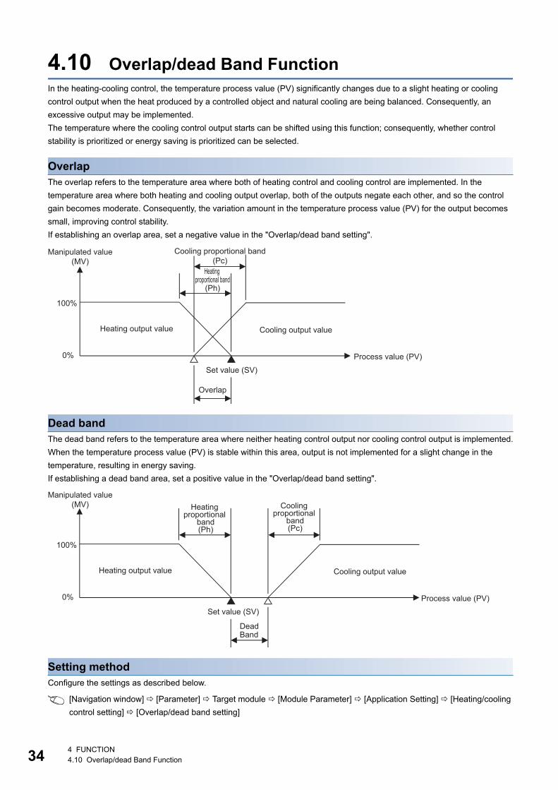
34
4.10 Overlap/dead Band FunctionIn the heating-cooling control, the temperature process value (PV) significantly changes due to a slight heating or cooling
control output when the heat produced by a controlled object and natural cooling are being balanced. Consequently, an
excessive output may be implemented.
The temperature where the cooling control output starts can be shifted using this function; consequently, whether control
stability is prioritized or energy saving is prioritized can be selected.
OverlapThe overlap refers to the temperature area where both of heating control and cooling control are implemented. In the
temperature area where both heating and cooling output overlap, both of the outputs negate each other, and so the control
gain becomes moderate. Consequently, the variation amount in the temperature process value (PV) for the output becomes
small, improving control stability.
If establishing an overlap area, set a negative value in the "Overlap/dead band setting".
Dead bandThe dead band refers to the temperature area where neither heating control output nor cooling control output is implemented.
When the temperature process value (PV) is stable within this area, output is not implemented for a slight change in the
temperature, resulting in energy saving.
If establishing a dead band area, set a positive value in the "Overlap/dead band setting".
Setting methodConfigure the settings as described below.
[Navigation window] [Parameter] Target module [Module Parameter] [Application Setting] [Heating/cooling
control setting] [Overlap/dead band setting]
100%
0%
Heating output value
Manipulated value(MV)
Heating proportional band
(Ph)
Cooling proportional band(Pc)
Set value (SV)
Cooling output value
Process value (PV)
Overlap
100%
0%
Heating output value
Manipulated value(MV) Heating
proportional band(Ph)
Cooling proportional
band(Pc)
Set value (SV)
DeadBand
Cooling output value
Process value (PV)
4 FUNCTION4.10 Overlap/dead Band Function
4
4.11 Cooling Method Setting FunctionThis function switches the cooling method depending on whether the cooling device is air-cooling type, water-cooling type, or
cooling gain linear type in the case of heating and cooling PID control. As the cooling characteristics between air cooling and
water cooling are very different, it is possible to request PID constants for the device by setting the cooling method when
implementing AT (auto tuning).
• Air-cooling type/water-cooling type
Uses an algorithm that presumes heating and cooling PID controls for plastic molding devices.
Good responsiveness and small set value response characteristics for over-travel amounts can be obtained even for devices
that have cooling configurations with non-linear characteristics.
• Cooling gain linear type
Uses an algorithm that presumes applications without non-linear cooling performance, such as electronic coolers that use
Peltier elements.
During auto tuning implementation, PID constants are calculated and the auto tuning is implemented based
on this setting. Consequently, more suitable PID constants can be calculated by the setting according to the
cooling characteristics of the device. For details on the auto tuning function, refer to the following.
Page 36 Auto Tuning Function
Setting methodConfigure the settings as described below.
[Navigation window] [Parameter] Target module [Module Parameter] [Application Setting] [Heating/cooling
control setting] [Cooling method setting]
• An operational expression of the auto tuning for the calculation of PID constants is determined based on this
setting. Consequently, always configure this setting before implementing auto tuning.
• Air cooling and water cooling roughly indicate the level of the cooling ability. When a device is too cooled
even though air cooling has been selected, set "1: Water cooling". When a device is less likely to be cooled
even though water cooling has been selected, set "0: Air cooling".
• Generally, the ability of water cooling is higher than that of air cooling and cooling may be too strong when
the same PID constants as the one for air cooling are used for water cooling. Consequently, it may take
some time for control to stabilize. Consequently, the auto tuning calculates PID constants so that the PID
constants of when "1: Water cooling" is set become larger than the ones of when "0: Air cooling" is set.
4 FUNCTION4.11 Cooling Method Setting Function 35
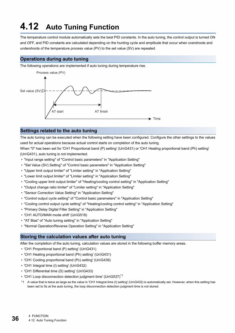
36
4.12 Auto Tuning FunctionThe temperature control module automatically sets the best PID constants. In the auto tuning, the control output is turned ON
and OFF, and PID constants are calculated depending on the hunting cycle and amplitude that occur when overshoots and
undershoots of the temperature process value (PV) to the set value (SV) are repeated.
Operations during auto tuningThe following operations are implemented if auto tuning during temperature rise.
Settings related to the auto tuningThe auto tuning can be executed when the following setting have been configured. Configure the other settings to the values
used for actual operations because actual control starts on completion of the auto tuning.
When "0" has been set for 'CH1 Proportional band (P) setting' (Un\G431) or 'CH1 Heating proportional band (Ph) setting'
(Un\G431), auto tuning is not implemented.
• "Input range setting" of "Control basic parameters" in "Application Setting"
• "Set Value (SV) Setting" of "Control basic parameters" in "Application Setting"
• "Upper limit output limiter" of "Limiter setting" in "Application Setting"
• "Lower limit output limiter" of "Limiter setting" in "Application Setting"
• "Cooling upper limit output limiter" of "Heating/cooling control setting" in "Application Setting"
• "Output change ratio limiter" of "Limiter setting" in "Application Setting"
• "Sensor Correction Value Setting" in "Application Setting"
• "Control output cycle setting" of "Control basic parameters" in "Application Setting"
• "Cooling control output cycle setting" of "Heating/cooling control setting" in "Application Setting"
• "Primary Delay Digital Filter Setting" in "Application Setting"
• 'CH1 AUTO/MAN mode shift' (Un\G518)
• "AT Bias" of "Auto tuning setting" in "Application Setting"
• "Normal Operation/Reverse Operation Setting" in "Application Setting"
Storing the calculation values after auto tuningAfter the completion of the auto tuning, calculation values are stored in the following buffer memory areas.
• 'CH1 Proportional band (P) setting' (Un\G431)
• 'CH1 Heating proportional band (Ph) setting' (Un\G431)
• 'CH1 Cooling proportional band (Pc) setting' (Un\G439)
• 'CH1 Integral time (I) setting' (Un\G432)
• 'CH1 Differential time (D) setting' (Un\G433)
• 'CH1 Loop disconnection detection judgment time' (Un\G537)*1
*1 A value that is twice as large as the value in 'CH1 Integral time (I) setting' (Un\G432) is automatically set. However, when this setting has been set to 0s at the auto tuning, the loop disconnection detection judgment time is not stored.
AT start
Time
Process value (PV)
AT finish
Set value (SV)
4 FUNCTION4.12 Auto Tuning Function
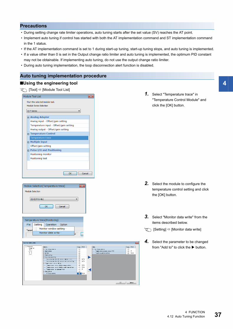
4
Precautions • During setting change rate limiter operations, auto tuning starts after the set value (SV) reaches the AT point.
• Implement auto tuning if control has started with both the AT implementation command and ST implementation command
in the 1 status.
• If the AT implementation command is set to 1 during start-up tuning, start-up tuning stops, and auto tuning is implemented.
• If a value other than 0 is set in the Output change ratio limiter and auto tuning is implemented, the optimum PID constant
may not be obtainable. If implementing auto tuning, do not use the output change ratio limiter.
• During auto tuning implementation, the loop disconnection alert function is disabled.
Auto tuning implementation procedure
■Using the engineering tool
[Tool] [Module Tool List]1. Select "Temperature trace" in
"Temperature Control Module" and
click the [OK] button.
2. Select the module to configure the
temperature control setting and click
the [OK] button.
3. Select "Monitor data write" from the
items described below.
[Setting] [Monitor data write]
4. Select the parameter to be changed
from "Add to" to click the button.
4 FUNCTION4.12 Auto Tuning Function 37
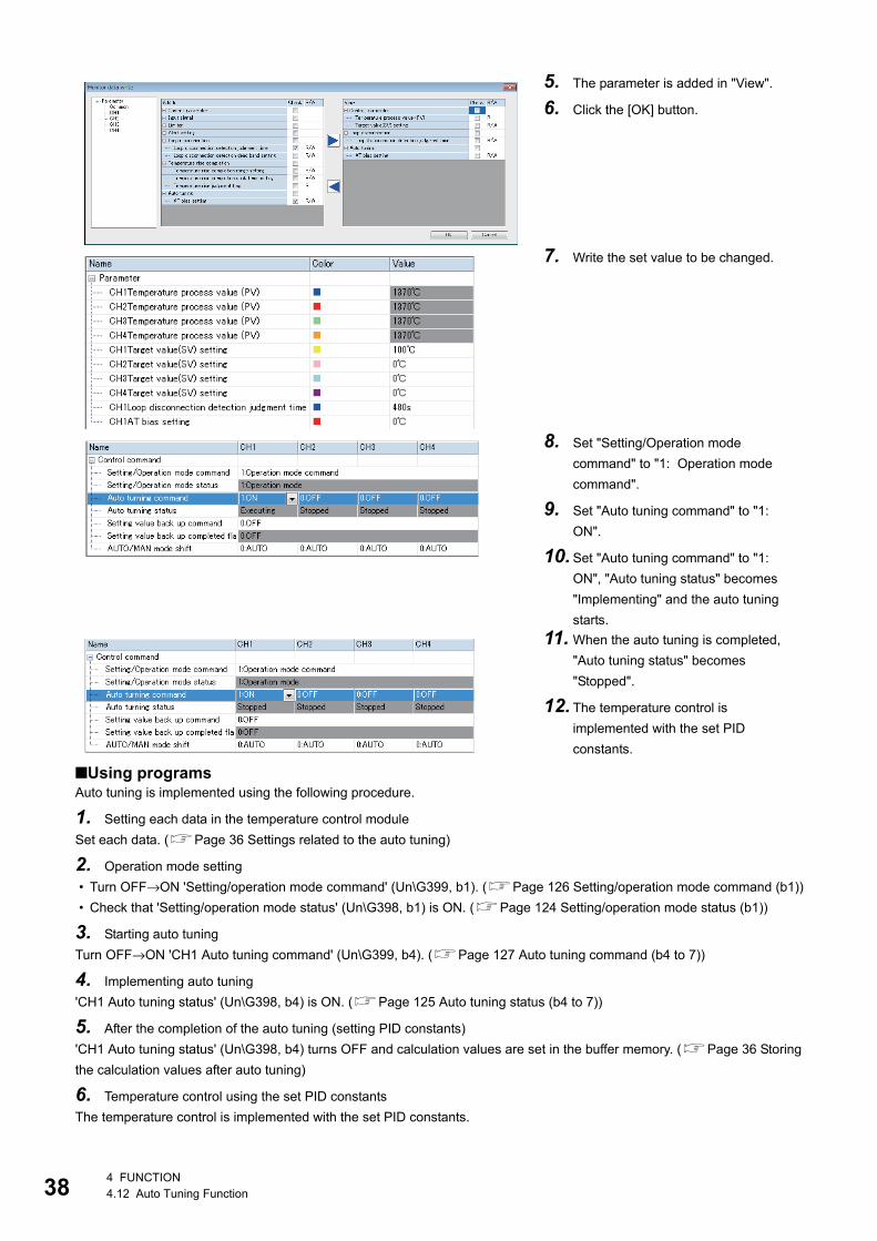
38
■Using programsAuto tuning is implemented using the following procedure.
1. Setting each data in the temperature control module
Set each data. (Page 36 Settings related to the auto tuning)
2. Operation mode setting
• Turn OFF→ON 'Setting/operation mode command' (Un\G399, b1). (Page 126 Setting/operation mode command (b1))
• Check that 'Setting/operation mode status' (Un\G398, b1) is ON. (Page 124 Setting/operation mode status (b1))
3. Starting auto tuning
Turn OFF→ON 'CH1 Auto tuning command' (Un\G399, b4). (Page 127 Auto tuning command (b4 to 7))
4. Implementing auto tuning
'CH1 Auto tuning status' (Un\G398, b4) is ON. (Page 125 Auto tuning status (b4 to 7))
5. After the completion of the auto tuning (setting PID constants)
'CH1 Auto tuning status' (Un\G398, b4) turns OFF and calculation values are set in the buffer memory. (Page 36 Storing
the calculation values after auto tuning)
6. Temperature control using the set PID constants
The temperature control is implemented with the set PID constants.
5. The parameter is added in "View".
6. Click the [OK] button.
7. Write the set value to be changed.
8. Set "Setting/Operation mode
command" to "1: Operation mode
command".
9. Set "Auto tuning command" to "1:
ON".
10. Set "Auto tuning command" to "1:
ON", "Auto tuning status" becomes
"Implementing" and the auto tuning
starts.
11. When the auto tuning is completed,
"Auto tuning status" becomes
"Stopped".
12. The temperature control is
implemented with the set PID
constants.
4 FUNCTION4.12 Auto Tuning Function
4
Auto tuning implementation conditions and stop conditions
■Auto tuning implementation conditionsIf all of the following conditions are satisfied, auto tuning can be implemented.
• AUTO/MAN mode switching is "0: AUTO mode"
• Operations mode setting is "3: Monitor + alert + control"
• Proportional band setting is other than 0
• The values of upper limit output limiter, heating upper limit output limiter, and cooling upper limit output limiter are all 1
(0.1%) min.
• The lower limit output limiter value is 999 (99.9%) max.
• No input value errors (upper limit/lower limit) have occurred
• Cascade ON/OFF is "0: Cascade OFF"
• AT/ST error completion flag is 0
■Auto tuning stop conditionsIf any of the following conditions occur during auto tuning, auto tuning force-ends, and the AT/ST error completion flag turns
ON.
• An input value error (upper limit/lower limit) occurs
• Control start/stop switching is changed to "0: Stop control"
• The set value (SV) is changed
• AUTO/MAN mode switching is changed to "1: MAN mode"
• Operations mode setting is changed to "3: Monitor + alert + control"
• 2-position operation is implemented (when proportional band is set to 0)
• The values in the upper limit outputs limiter, heating upper limit outputs limiter, cooling upper limit outputs limiter, and the
lower limit outputs limiter are changed
• The sensor correction value is changed
• The primary delay digital filter value is changed
• The AT bias value is changed
• Normal Operation/Reverse Operation setting is changed
• Cooling method setting is changed
• The target value, AT bias, or settings limiter is changed, and the AT point (= Set value (SV) + AT bias) is outside the settings
limiter range
• Cascade ON/OFF is changed to "1: Cascade ON"
• Auto tuning does not finish even if approx. 2 hours has elapsed since auto tuning started
• A hardware error (24 V DC power supply error, cooling contact temperature compensation error, or A/D converter error) is
detected
• The calculated value of the auto tuning PID constant exceeds the settings range
4 FUNCTION4.12 Auto Tuning Function 39
40
4.13 AT (Auto Tuning) Bias FunctionIf the process value (PV) does not exceed the set value (SV) during auto tuning implementation, AT bias is set.
Auto tuning implements 2-position control on the set value (SV), and calculates and sets the PID constants by hunting the
process value (PV). Depending on the control target, however, auto tuning using hunting may be poor. In such cases, the auto
tuning set value (SV)= AT point can be changed using the AT bias settings.
Ex.
When a negative value has been set for AT bias (Reverse Operation)
Precautions
• If the set value (SV) + AT bias (=AT point) is outside the settings limiter range, auto tuning is implemented using the settings
limiter value.
• If the setting change rate limiter setting is other than 0 when auto tuning starts, the set value (SV) changes according to the
settings variation rate limiter setting until the AT point is reached. At this time, the event AT implementation status
(Un\G429, b14) turns ON after the set value reaches the AT point, and auto tuning starts.
Setting methodConfigure the settings as described below.
[Navigation window] [Parameter] Target module [Module Parameter] [Application Setting] [Auto tuning
setting][AT bias]
(1) 'CH1 AT bias' (Un\G546)
(1)
Temperature process value (PV)
Time
Set value (SV)
AT point
4 FUNCTION4.13 AT (Auto Tuning) Bias Function
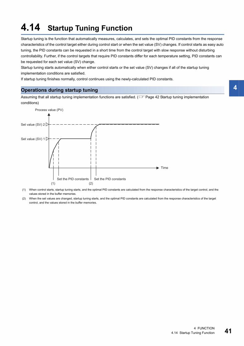
4
4.14 Startup Tuning FunctionStartup tuning is the function that automatically measures, calculates, and sets the optimal PID constants from the response
characteristics of the control target either during control start or when the set value (SV) changes. If control starts as easy auto
tuning, the PID constants can be requested in a short time from the control target with slow response without disturbing
controllability. Further, if the control targets that require PID constants differ for each temperature setting, PID constants can
be requested for each set value (SV) change.
Startup tuning starts automatically when either control starts or the set value (SV) changes if all of the startup tuning
implementation conditions are satisfied.
If startup tuning finishes normally, control continues using the newly-calculated PID constants.
Operations during startup tuningAssuming that all startup tuning implementation functions are satisfied. (Page 42 Startup tuning implementation
conditions)
(1) When control starts, startup tuning starts, and the optimal PID constants are calculated from the response characteristics of the target control, and the
values stored in the buffer memories.
(2) When the set values are changed, startup tuning starts, and the optimal PID constants are calculated from the response characteristics of the target
control, and the values stored in the buffer memories.
(1) (2)
Time
Process value (PV)
Set value (SV) 1
Set value (SV) 2
Set the PID constants Set the PID constants
4 FUNCTION4.14 Startup Tuning Function 41
42
Startup tuning implementation conditions and stop conditions
■Startup tuning implementation conditionsIf all of the following conditions are satisfied, startup tuning can be implemented.
• AUTO/MAN mode switching is "0: AUTO mode"
• Operations mode setting is "3: Monitor + alert + control"
• Proportional band setting is other than 0
• The values of upper limit output limiter, heating upper limit output limiter, and cooling upper limit output limiter are all 1
(0.1%) min.
• The lower limit output limiter value is 999 (99.9%) max.
• No input value errors (upper limit/lower limit) have occurred
• Cascade ON/OFF is "0: Cascade OFF"
• If using startup tuning when changing set values (SV), the process value (PV) is stable
• Outputs change when startup tuning starts, and are saturated by the upper limit outputs limiter or the lower limit outputs
limited
• In startup tuning when control starts, the difference between the process value (PV) and set value (SV) is x2 or greater than
the proportional band
• AT implementation command is 0
• AT/ST error completion flag is 0
■Startup tuning stop conditionsIf any of the following conditions occur during startup tuning, startup tuning force-ends, and the AT/ST error completion flag
turns ON.
• An input value error (upper limit/lower limit) occurs
• Control start/stop switching is changed to "0: Stop control"
• AUTO/MAN mode switching is changed to "1: MAN mode"
• Operations mode setting is changed to "3: Monitor + alert + control"
• 2-position operation is implemented (when proportional band is set to 0)
• The values in the upper limit outputs limiter, heating upper limit outputs limiter, cooling upper limit outputs limiter, and the
lower limit outputs limiter are changed
• The sensor correction value is changed
• The primary delay digital filter value is changed
• Cascade ON/OFF is changed to "1: Cascade ON"
• Startup tuning does not finish even if approx. 100 mins. has elapsed since startup tuning started
• A hardware error (24 V DC power supply error, cooling contact temperature compensation error, or A/D converter error) is
detected
• AT implementation command is set to 1
• Manipulated value saturation time is too short
• The calculated value of the startup tuning PID constant exceeds the settings range
Precautions • To implement startup tuning when control starts, make sure to turn ON the heater power supply at the same time or before
starting startup tuning.
• Start startup tuning when the difference between the process value (PV) and set value (SV) is x2 or greater than the
proportional band when startup tuning starts.
• If limiting the manipulated value using the output limiter, the optimal PID constants may not be obtainable even if startup
tuning was implemented.
• If the output change ratio limiter is set, the optimal PID constants may not be obtainable even if startup tuning was
implemented.
• During data measurements for calculations, an error completion may occur if the set value (SV) is changed so that the
manipulated output is excluded from the saturation status.
4 FUNCTION4.14 Startup Tuning Function
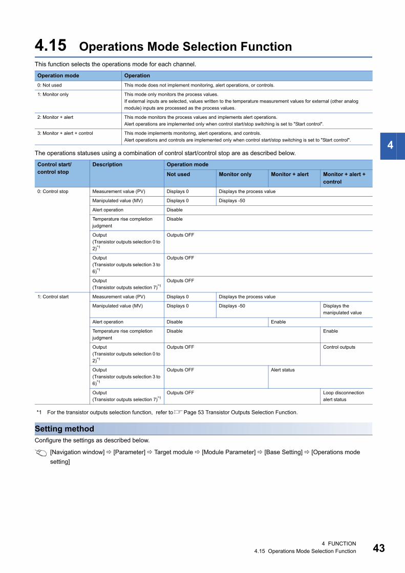
4
4.15 Operations Mode Selection FunctionThis function selects the operations mode for each channel.
The operations statuses using a combination of control start/control stop are as described below.
*1 For the transistor outputs selection function, refer toPage 53 Transistor Outputs Selection Function.
Setting methodConfigure the settings as described below.
[Navigation window] [Parameter] Target module [Module Parameter] [Base Setting] [Operations mode
setting]
Operation mode Operation
0: Not used This mode does not implement monitoring, alert operations, or controls.
1: Monitor only This mode only monitors the process values.
If external inputs are selected, values written to the temperature measurement values for external (other analog
module) inputs are processed as the process values.
2: Monitor + alert This mode monitors the process values and implements alert operations.
Alert operations are implemented only when control start/stop switching is set to "Start control".
3: Monitor + alert + control This mode implements monitoring, alert operations, and controls.
Alert operations and controls are implemented only when control start/stop switching is set to "Start control".
Control start/control stop
Description Operation mode
Not used Monitor only Monitor + alert Monitor + alert + control
0: Control stop Measurement value (PV) Displays 0 Displays the process value
Manipulated value (MV) Displays 0 Displays -50
Alert operation Disable
Temperature rise completion
judgment
Disable
Output
(Transistor outputs selection 0 to
2)*1
Outputs OFF
Output
(Transistor outputs selection 3 to
6)*1
Outputs OFF
Output
(Transistor outputs selection 7)*1Outputs OFF
1: Control start Measurement value (PV) Displays 0 Displays the process value
Manipulated value (MV) Displays 0 Displays -50 Displays the
manipulated value
Alert operation Disable Enable
Temperature rise completion
judgment
Disable Enable
Output
(Transistor outputs selection 0 to
2)*1
Outputs OFF Control outputs
Output
(Transistor outputs selection 3 to
6)*1
Outputs OFF Alert status
Output
(Transistor outputs selection 7)*1Outputs OFF Loop disconnection
alert status
4 FUNCTION4.15 Operations Mode Selection Function 43
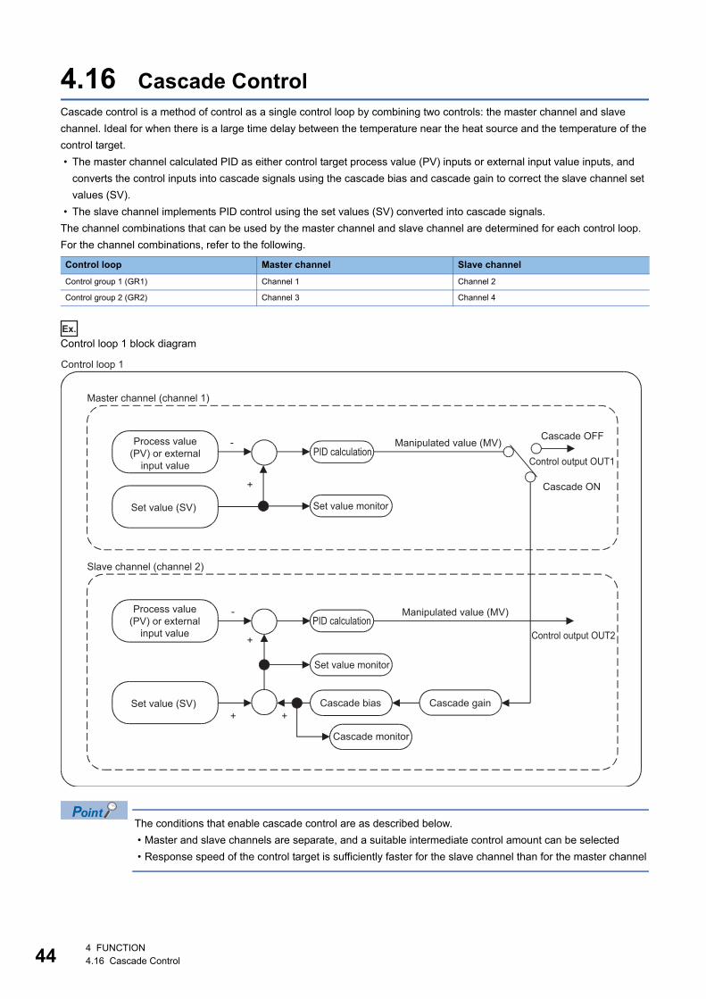
44
4.16 Cascade ControlCascade control is a method of control as a single control loop by combining two controls: the master channel and slave
channel. Ideal for when there is a large time delay between the temperature near the heat source and the temperature of the
control target.
• The master channel calculated PID as either control target process value (PV) inputs or external input value inputs, and
converts the control inputs into cascade signals using the cascade bias and cascade gain to correct the slave channel set
values (SV).
• The slave channel implements PID control using the set values (SV) converted into cascade signals.
The channel combinations that can be used by the master channel and slave channel are determined for each control loop.
For the channel combinations, refer to the following.
Ex.
Control loop 1 block diagram
The conditions that enable cascade control are as described below.
• Master and slave channels are separate, and a suitable intermediate control amount can be selected
• Response speed of the control target is sufficiently faster for the slave channel than for the master channel
Control loop Master channel Slave channel
Control group 1 (GR1) Channel 1 Channel 2
Control group 2 (GR2) Channel 3 Channel 4
Cascade ON
Cascade OFF
PID calculation
Set value monitor
Set value monitor
Set value (SV)
+
-
Set value (SV)
+
+ +
-
Control output OUT1
Control output OUT2
Master channel (channel 1)
Slave channel (channel 2)
PID calculation
Control loop 1
Manipulated value (MV)
Manipulated value (MV)
Process value (PV) or external
input value
Process value (PV) or external
input value
Cascade bias
Cascade monitor
Cascade gain
4 FUNCTION4.16 Cascade Control
4
Precautions
• Depending on the control conditions, it may be necessary to limit the movement area of the slave controller using "cascade
gain" and "cascade bias".
• During cascade control, auto tuning and startup tuning cannot be implemented.
Setting methodConfigure the settings as described below.
[Navigation window] [Parameter] Target module [Module Parameter] [Application Setting] [Cascade
function]
Tuning during cascade controlDuring cascade control, tuning (auto tuning and startup tuning) cannot be used. Turn OFF cascade control before
implementing tuning, and set benchmark PID constants.
Implement tuning for each channel separately, and stop control for the channels that are not to be tuned. (Set the operations
mode settings to "0: Not used", "1: Monitor only", or "2: Monitor + alert".)
■Tuning procedure example
1. Set only the slave channel to control status and implement auto tuning to request the slave channel PID constants.
Implementing PID control on both the master and slave channels during cascade control may cause integral
operations to raise the low frequency gain too high, causing slow cycle vibration response in one or other of
the channels.
Consequently, generally set the slave channel so that this phenomenon does not occur using either P control
(I=0, D=0) or PD control (I=0).
Either the P control constant or PD control constant determines the auto tuning results implemented by the
slave channel as standard, and sets the proportional band to approx. x1.4.
2. Set only the master channel to control status and implement auto tuning to request the master channel PID constants.
3. Set the same master channel and slave channel set values (SV).
4. Turn OFF cascade status, and implement control for the slave channel only. Set the master channel operations mode to
either "1: Monitor" or "2: Monitor + alert", and wire control outputs for the slave channel only.
5. When the master and slave channel process values (PV) are stable, request the difference En in the process values (PV)
between the master channel and the slave channel. (Master channel process value (PV) - slave channel process value
(PV))
6. Set the slave channel set value range to approx. x4 the process value difference En determined in Step 5, and set the
cascade gain. (Slave channel set value range ÷ slave channel inputs range span)
7. Set the cascade bias. (Slave channel set value range ÷ 2)
8. Set the slave channel set value. (Master channel set value (SV) - Process value difference En)
9. Set the master channel operations mode setting to "3: Monitor + alert + control", and turn ON cascade control. Check the
control status while manually adjusting the master channel PID constants.
4 FUNCTION4.16 Cascade Control 45
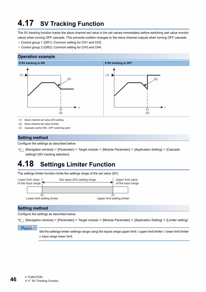
46
4.17 SV Tracking FunctionThe SV tracking function tracks the slave channel set value in the set values immediately before switching (set value monitor
value) when turning OFF cascade. This prevents sudden changes to the slave channel outputs when turning OFF cascade.
• Control group 1 (GR1): Common setting for CH1 and CH2.
• Control group 2 (GR2): Common setting for CH3 and CH4.
Operation example
Setting methodConfigure the settings as described below.
[Navigation window] [Parameter] Target module [Module Parameter] [Application Setting] [Cascade
setting][SV tracking selection]
4.18 Settings Limiter FunctionThe settings limiter function limits the settings range of the set value (SV).
Setting methodConfigure the settings as described below.
[Navigation window] [Parameter] Target module [Module Parameter] [Application Setting] [Limiter setting]
Set the settings limiter settings range using the inputs range upper limit ≥ upper limit limiter ≥ lower limit limiter
≥ input range lower limit.
If SV tracking is ON If SV tracking is OFF
(1) Slave channel set value (SV) setting
(2) Slave channel set value monitor
(3) Cascade control ON→OFF switching point
t
(1)(2)
(3)
t
(1)(2)
(3)
Lower limit setting limiter Upper limit setting limiter
Set value (SV) setting rangeLower limit value of the input range
Upper limit value of the input range
4 FUNCTION4.17 SV Tracking Function
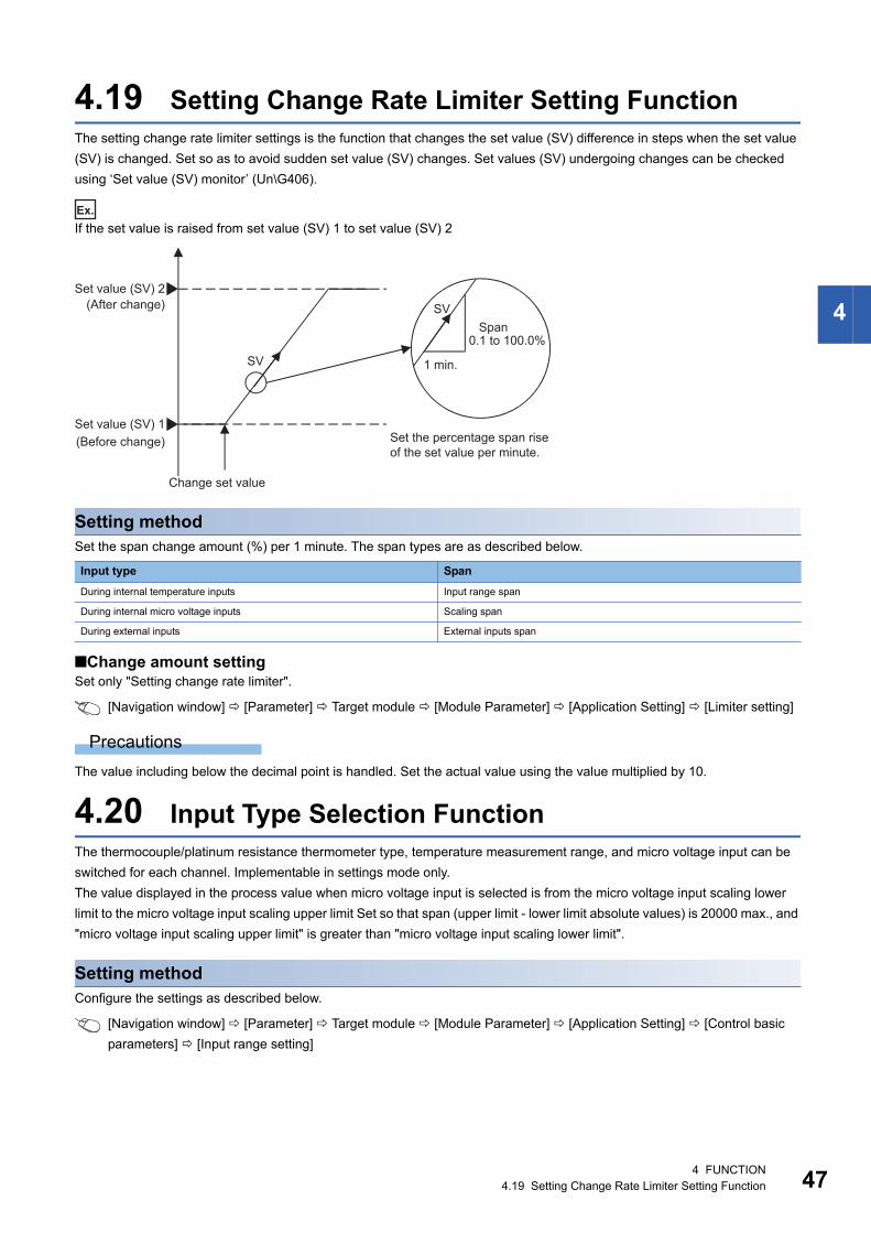
4
4.19 Setting Change Rate Limiter Setting FunctionThe setting change rate limiter settings is the function that changes the set value (SV) difference in steps when the set value
(SV) is changed. Set so as to avoid sudden set value (SV) changes. Set values (SV) undergoing changes can be checked
using ‘Set value (SV) monitor’ (Un\G406).
Ex.
If the set value is raised from set value (SV) 1 to set value (SV) 2
Setting methodSet the span change amount (%) per 1 minute. The span types are as described below.
■Change amount settingSet only "Setting change rate limiter".
[Navigation window] [Parameter] Target module [Module Parameter] [Application Setting] [Limiter setting]
Precautions
The value including below the decimal point is handled. Set the actual value using the value multiplied by 10.
4.20 Input Type Selection FunctionThe thermocouple/platinum resistance thermometer type, temperature measurement range, and micro voltage input can be
switched for each channel. Implementable in settings mode only.
The value displayed in the process value when micro voltage input is selected is from the micro voltage input scaling lower
limit to the micro voltage input scaling upper limit Set so that span (upper limit - lower limit absolute values) is 20000 max., and
"micro voltage input scaling upper limit" is greater than "micro voltage input scaling lower limit".
Setting methodConfigure the settings as described below.
[Navigation window] [Parameter] Target module [Module Parameter] [Application Setting] [Control basic
parameters] [Input range setting]
Input type Span
During internal temperature inputs Input range span
During internal micro voltage inputs Scaling span
During external inputs External inputs span
Span0.1 to 100.0%
1 min.
Change set value
SV
SV
Set value (SV) 2
Set value (SV) 1
(Before change)
(After change)
Set the percentage span rise of the set value per minute.
4 FUNCTION4.19 Setting Change Rate Limiter Setting Function 47
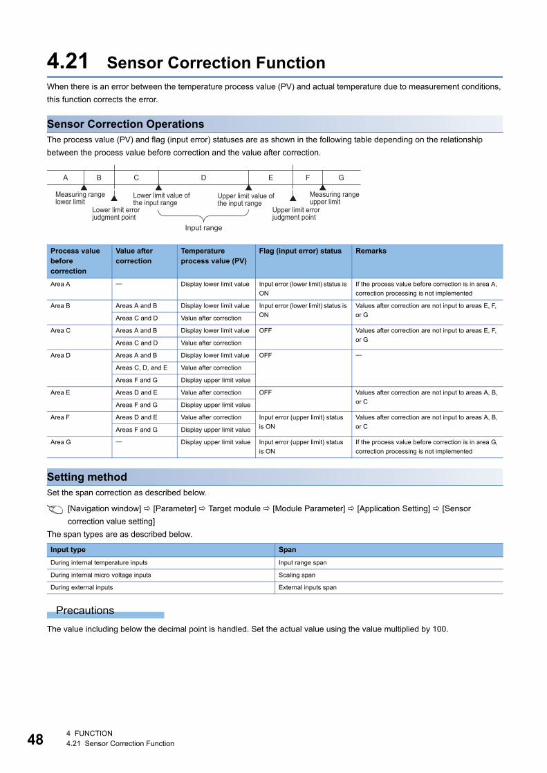
48
4.21 Sensor Correction FunctionWhen there is an error between the temperature process value (PV) and actual temperature due to measurement conditions,
this function corrects the error.
Sensor Correction OperationsThe process value (PV) and flag (input error) statuses are as shown in the following table depending on the relationship
between the process value before correction and the value after correction.
Setting methodSet the span correction as described below.
[Navigation window] [Parameter] Target module [Module Parameter] [Application Setting] [Sensor
correction value setting]
The span types are as described below.
Precautions
The value including below the decimal point is handled. Set the actual value using the value multiplied by 100.
Process value before correction
Value after correction
Temperature process value (PV)
Flag (input error) status Remarks
Area A Display lower limit value Input error (lower limit) status is
ON
If the process value before correction is in area A,
correction processing is not implemented
Area B Areas A and B Display lower limit value Input error (lower limit) status is
ON
Values after correction are not input to areas E, F,
or GAreas C and D Value after correction
Area C Areas A and B Display lower limit value OFF Values after correction are not input to areas E, F,
or GAreas C and D Value after correction
Area D Areas A and B Display lower limit value OFF
Areas C, D, and E Value after correction
Areas F and G Display upper limit value
Area E Areas D and E Value after correction OFF Values after correction are not input to areas A, B,
or CAreas F and G Display upper limit value
Area F Areas D and E Value after correction Input error (upper limit) status
is ON
Values after correction are not input to areas A, B,
or CAreas F and G Display upper limit value
Area G Display upper limit value Input error (upper limit) status
is ON
If the process value before correction is in area G,
correction processing is not implemented
Input type Span
During internal temperature inputs Input range span
During internal micro voltage inputs Scaling span
During external inputs External inputs span
A
Measuring range lower limit
Lower limit value of the input range
Upper limit value of the input range
Input range
Measuring range upper limit
Upper limit error judgment point
Lower limit error judgment point
B C D E F G
4 FUNCTION4.21 Sensor Correction Function
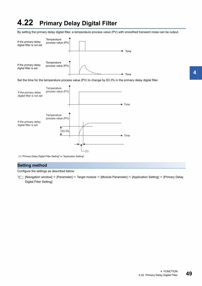
4
4.22 Primary Delay Digital FilterBy setting the primary delay digital filter, a temperature process value (PV) with smoothed transient noise can be output.
Set the time for the temperature process value (PV) to change by 63.3% in the primary delay digital filter.
Setting methodConfigure the settings as described below.
[Navigation window] [Parameter] Target module [Module Parameter] [Application Setting] [Primary Delay
Digital Filter Setting]
(1) "Primary Delay Digital Filter Setting" in "Application Setting"
Time
Time
Temperature process value (PV)
Temperature process value (PV)
If the primary delay digital filter is not set
If the primary delay digital filter is set
(1)
63.3%
Time
Time
Temperature process value (PV)
Temperature process value (PV)If the primary delay
digital filter is not set
If the primary delay digital filter is set
4 FUNCTION4.22 Primary Delay Digital Filter 49
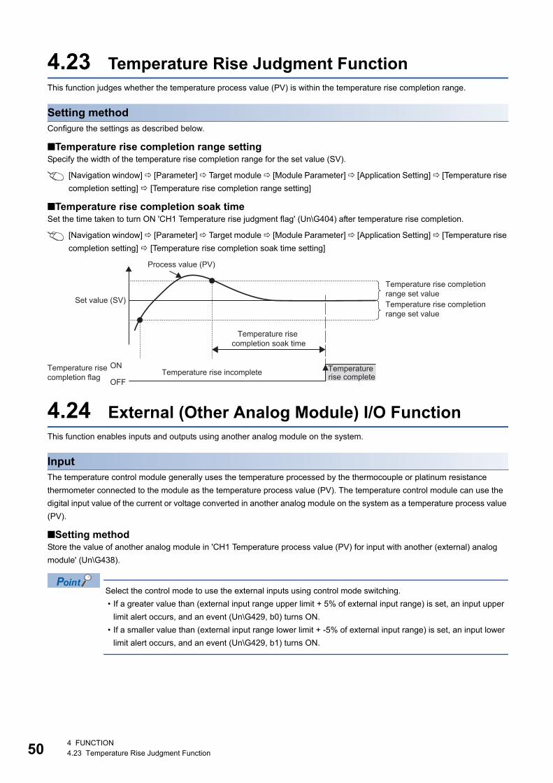
50
4.23 Temperature Rise Judgment FunctionThis function judges whether the temperature process value (PV) is within the temperature rise completion range.
Setting methodConfigure the settings as described below.
■Temperature rise completion range settingSpecify the width of the temperature rise completion range for the set value (SV).
[Navigation window] [Parameter] Target module [Module Parameter] [Application Setting] [Temperature rise
completion setting] [Temperature rise completion range setting]
■Temperature rise completion soak timeSet the time taken to turn ON 'CH1 Temperature rise judgment flag' (Un\G404) after temperature rise completion.
[Navigation window] [Parameter] Target module [Module Parameter] [Application Setting] [Temperature rise
completion setting] [Temperature rise completion soak time setting]
4.24 External (Other Analog Module) I/O FunctionThis function enables inputs and outputs using another analog module on the system.
InputThe temperature control module generally uses the temperature processed by the thermocouple or platinum resistance
thermometer connected to the module as the temperature process value (PV). The temperature control module can use the
digital input value of the current or voltage converted in another analog module on the system as a temperature process value
(PV).
■Setting methodStore the value of another analog module in 'CH1 Temperature process value (PV) for input with another (external) analog
module' (Un\G438).
Select the control mode to use the external inputs using control mode switching.
• If a greater value than (external input range upper limit + 5% of external input range) is set, an input upper
limit alert occurs, and an event (Un\G429, b0) turns ON.
• If a smaller value than (external input range lower limit + -5% of external input range) is set, an input lower
limit alert occurs, and an event (Un\G429, b1) turns ON.
Temperature rise completionrange set valueTemperature rise completionrange set value
Temperature rise completion flag
Set value (SV)
Temperature rise completion soak time
Temperature rise incomplete
Process value (PV)
ON
OFF
Temperature rise complete
4 FUNCTION4.23 Temperature Rise Judgment Function
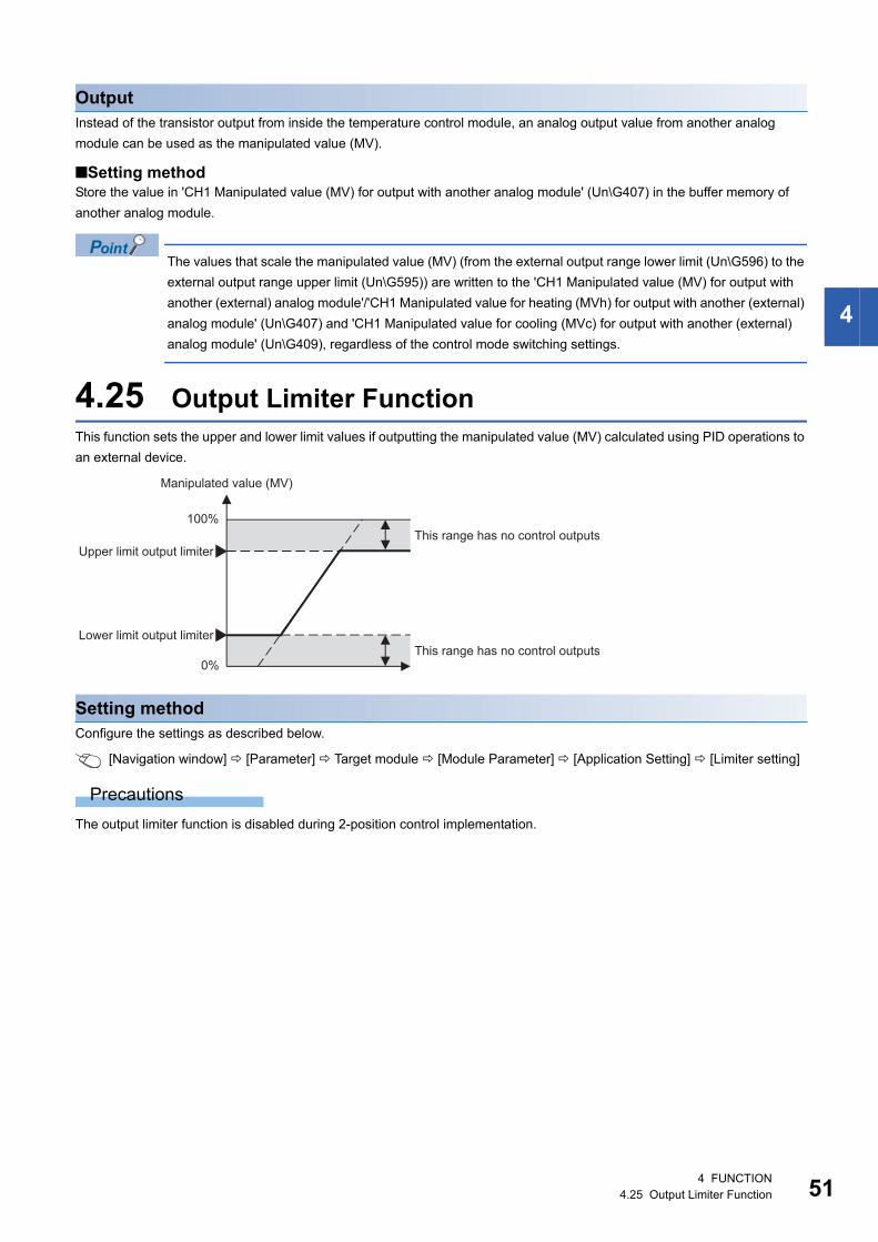
4
OutputInstead of the transistor output from inside the temperature control module, an analog output value from another analog
module can be used as the manipulated value (MV).
■Setting methodStore the value in 'CH1 Manipulated value (MV) for output with another analog module' (Un\G407) in the buffer memory of
another analog module.
The values that scale the manipulated value (MV) (from the external output range lower limit (Un\G596) to the
external output range upper limit (Un\G595)) are written to the 'CH1 Manipulated value (MV) for output with
another (external) analog module'/'CH1 Manipulated value for heating (MVh) for output with another (external)
analog module' (Un\G407) and 'CH1 Manipulated value for cooling (MVc) for output with another (external)
analog module' (Un\G409), regardless of the control mode switching settings.
4.25 Output Limiter FunctionThis function sets the upper and lower limit values if outputting the manipulated value (MV) calculated using PID operations to
an external device.
Setting methodConfigure the settings as described below.
[Navigation window] [Parameter] Target module [Module Parameter] [Application Setting] [Limiter setting]
Precautions
The output limiter function is disabled during 2-position control implementation.
Upper limit output limiter
Lower limit output limiter
100%
0%
Manipulated value (MV)
This range has no control outputs
This range has no control outputs
4 FUNCTION4.25 Output Limiter Function 51
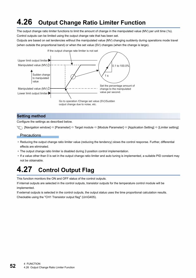
52
4.26 Output Change Ratio Limiter FunctionThe output change ratio limiter functions to limit the amount of change in the manipulated value (MV) per unit time (1s).
Control outputs can be limited using the output change rate that has been set.
Outputs are based on set tendencies without the manipulated value (MV) changing suddenly during operations mode travel
(when outside the proportional band) or when the set value (SV) changes (when the change is large).
Setting methodConfigure the settings as described below.
[Navigation window] [Parameter] Target module [Module Parameter] [Application Setting] [Limiter setting]
Precautions
• Reducing the output change ratio limiter value (reducing the tendency) slows the control response. Further, differential
effects are eliminated.
• The output change ratio limiter is disabled during 2-position control implementation.
• If a value other than 0 is set in the output change ratio limiter and auto tuning is implemented, a suitable PID constant may
not be obtainable.
4.27 Control Output FlagThis function monitors the ON and OFF status of the control outputs.
If internal outputs are selected in the control outputs, transistor outputs for the temperature control module will be
implemented.
If external outputs is selected in the control outputs, the output status uses the time proportional calculation results.
Checkable using the "CH1 Transistor output flag" (Un\G405).
If the output change rate limiter is not set
0.1 to 100.0%
1 s
Upper limit output limiter
Lower limit output limiter
Manipulated value (MV)
Manipulated value (MV)
Sudden change to manipulated value
Go to operation /Change set value (SV)/Sudden output change due to noise, etc.
Set the percentage amount of change to the manipulated value per second.
4 FUNCTION4.26 Output Change Ratio Limiter Function
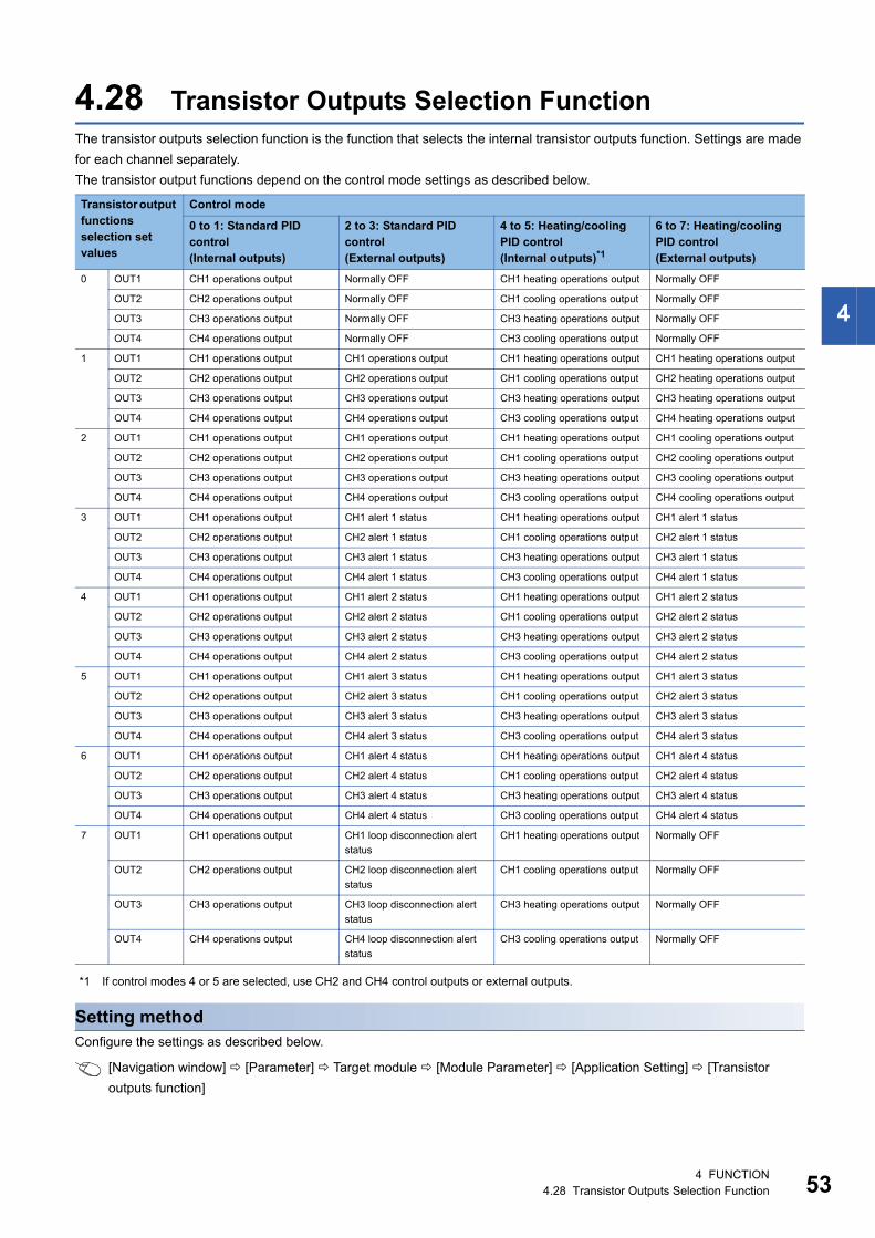
4
4.28 Transistor Outputs Selection FunctionThe transistor outputs selection function is the function that selects the internal transistor outputs function. Settings are made
for each channel separately.
The transistor output functions depend on the control mode settings as described below.
*1 If control modes 4 or 5 are selected, use CH2 and CH4 control outputs or external outputs.
Setting methodConfigure the settings as described below.
[Navigation window] [Parameter] Target module [Module Parameter] [Application Setting] [Transistor
outputs function]
Transistor output functions selection set values
Control mode
0 to 1: Standard PID control(Internal outputs)
2 to 3: Standard PID control(External outputs)
4 to 5: Heating/cooling PID control(Internal outputs)*1
6 to 7: Heating/cooling PID control(External outputs)
0 OUT1 CH1 operations output Normally OFF CH1 heating operations output Normally OFF
OUT2 CH2 operations output Normally OFF CH1 cooling operations output Normally OFF
OUT3 CH3 operations output Normally OFF CH3 heating operations output Normally OFF
OUT4 CH4 operations output Normally OFF CH3 cooling operations output Normally OFF
1 OUT1 CH1 operations output CH1 operations output CH1 heating operations output CH1 heating operations output
OUT2 CH2 operations output CH2 operations output CH1 cooling operations output CH2 heating operations output
OUT3 CH3 operations output CH3 operations output CH3 heating operations output CH3 heating operations output
OUT4 CH4 operations output CH4 operations output CH3 cooling operations output CH4 heating operations output
2 OUT1 CH1 operations output CH1 operations output CH1 heating operations output CH1 cooling operations output
OUT2 CH2 operations output CH2 operations output CH1 cooling operations output CH2 cooling operations output
OUT3 CH3 operations output CH3 operations output CH3 heating operations output CH3 cooling operations output
OUT4 CH4 operations output CH4 operations output CH3 cooling operations output CH4 cooling operations output
3 OUT1 CH1 operations output CH1 alert 1 status CH1 heating operations output CH1 alert 1 status
OUT2 CH2 operations output CH2 alert 1 status CH1 cooling operations output CH2 alert 1 status
OUT3 CH3 operations output CH3 alert 1 status CH3 heating operations output CH3 alert 1 status
OUT4 CH4 operations output CH4 alert 1 status CH3 cooling operations output CH4 alert 1 status
4 OUT1 CH1 operations output CH1 alert 2 status CH1 heating operations output CH1 alert 2 status
OUT2 CH2 operations output CH2 alert 2 status CH1 cooling operations output CH2 alert 2 status
OUT3 CH3 operations output CH3 alert 2 status CH3 heating operations output CH3 alert 2 status
OUT4 CH4 operations output CH4 alert 2 status CH3 cooling operations output CH4 alert 2 status
5 OUT1 CH1 operations output CH1 alert 3 status CH1 heating operations output CH1 alert 3 status
OUT2 CH2 operations output CH2 alert 3 status CH1 cooling operations output CH2 alert 3 status
OUT3 CH3 operations output CH3 alert 3 status CH3 heating operations output CH3 alert 3 status
OUT4 CH4 operations output CH4 alert 3 status CH3 cooling operations output CH4 alert 3 status
6 OUT1 CH1 operations output CH1 alert 4 status CH1 heating operations output CH1 alert 4 status
OUT2 CH2 operations output CH2 alert 4 status CH1 cooling operations output CH2 alert 4 status
OUT3 CH3 operations output CH3 alert 4 status CH3 heating operations output CH3 alert 4 status
OUT4 CH4 operations output CH4 alert 4 status CH3 cooling operations output CH4 alert 4 status
7 OUT1 CH1 operations output CH1 loop disconnection alert
status
CH1 heating operations output Normally OFF
OUT2 CH2 operations output CH2 loop disconnection alert
status
CH1 cooling operations output Normally OFF
OUT3 CH3 operations output CH3 loop disconnection alert
status
CH3 heating operations output Normally OFF
OUT4 CH4 operations output CH4 loop disconnection alert
status
CH3 cooling operations output Normally OFF
4 FUNCTION4.28 Transistor Outputs Selection Function 53
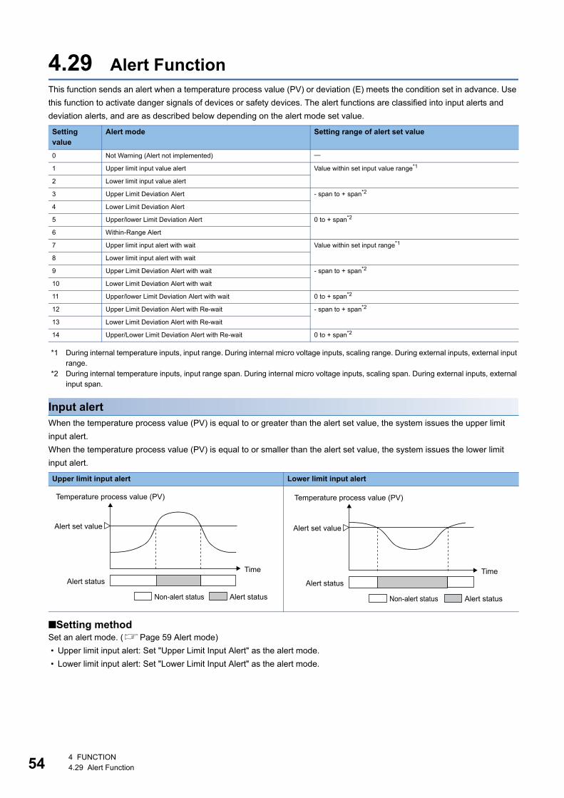
54
4.29 Alert FunctionThis function sends an alert when a temperature process value (PV) or deviation (E) meets the condition set in advance. Use
this function to activate danger signals of devices or safety devices. The alert functions are classified into input alerts and
deviation alerts, and are as described below depending on the alert mode set value.
*1 During internal temperature inputs, input range. During internal micro voltage inputs, scaling range. During external inputs, external input range.
*2 During internal temperature inputs, input range span. During internal micro voltage inputs, scaling span. During external inputs, external input span.
Input alertWhen the temperature process value (PV) is equal to or greater than the alert set value, the system issues the upper limit
input alert.
When the temperature process value (PV) is equal to or smaller than the alert set value, the system issues the lower limit
input alert.
■Setting methodSet an alert mode. (Page 59 Alert mode)
• Upper limit input alert: Set "Upper Limit Input Alert" as the alert mode.
• Lower limit input alert: Set "Lower Limit Input Alert" as the alert mode.
Setting value
Alert mode Setting range of alert set value
0 Not Warning (Alert not implemented)
1 Upper limit input value alert Value within set input value range*1
2 Lower limit input value alert
3 Upper Limit Deviation Alert - span to + span*2
4 Lower Limit Deviation Alert
5 Upper/lower Limit Deviation Alert 0 to + span*2
6 Within-Range Alert
7 Upper limit input alert with wait Value within set input range*1
8 Lower limit input alert with wait
9 Upper Limit Deviation Alert with wait - span to + span*2
10 Lower Limit Deviation Alert with wait
11 Upper/lower Limit Deviation Alert with wait 0 to + span*2
12 Upper Limit Deviation Alert with Re-wait - span to + span*2
13 Lower Limit Deviation Alert with Re-wait
14 Upper/Lower Limit Deviation Alert with Re-wait 0 to + span*2
Upper limit input alert Lower limit input alert
Non-alert status Alert status
Time
Temperature process value (PV)
Alert status
Alert set value
Non-alert status Alert status
Time
Temperature process value (PV)
Alert status
Alert set value
4 FUNCTION4.29 Alert Function
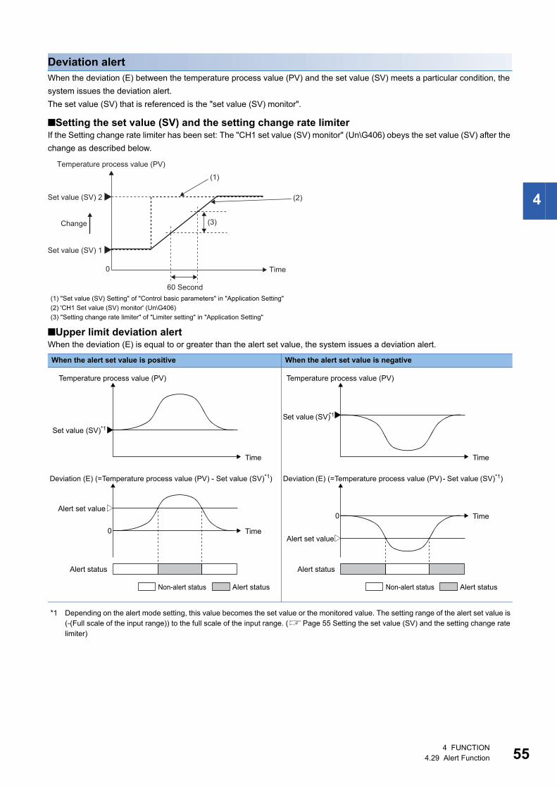
4
Deviation alertWhen the deviation (E) between the temperature process value (PV) and the set value (SV) meets a particular condition, the
system issues the deviation alert.
The set value (SV) that is referenced is the "set value (SV) monitor".
■Setting the set value (SV) and the setting change rate limiterIf the Setting change rate limiter has been set: The "CH1 set value (SV) monitor" (Un\G406) obeys the set value (SV) after the
change as described below.
■Upper limit deviation alertWhen the deviation (E) is equal to or greater than the alert set value, the system issues a deviation alert.
*1 Depending on the alert mode setting, this value becomes the set value or the monitored value. The setting range of the alert set value is (-(Full scale of the input range)) to the full scale of the input range. (Page 55 Setting the set value (SV) and the setting change rate limiter)
(1) "Set value (SV) Setting" of "Control basic parameters" in "Application Setting"
(2) 'CH1 Set value (SV) monitor' (Un\G406)
(3) "Setting change rate limiter" of "Limiter setting" in "Application Setting"
When the alert set value is positive When the alert set value is negative
(1)
(2)
(3)
60 Second
0
Set value (SV) 1
Change
Temperature process value (PV)
Time
Set value (SV) 2
Non-alert status Alert status
Time
Deviation (E) (=Temperature process value (PV) - Set value (SV)*1)
Alert status
0
Alert set value
Time
Temperature process value (PV)
Set value (SV)*1
Non-alert status Alert status
Time
Deviation (E) (=Temperature process value (PV) - Set value (SV)*1)
Alert status
0
Alert set value
Time
Temperature process value (PV)
Set value (SV)*1
4 FUNCTION4.29 Alert Function 55
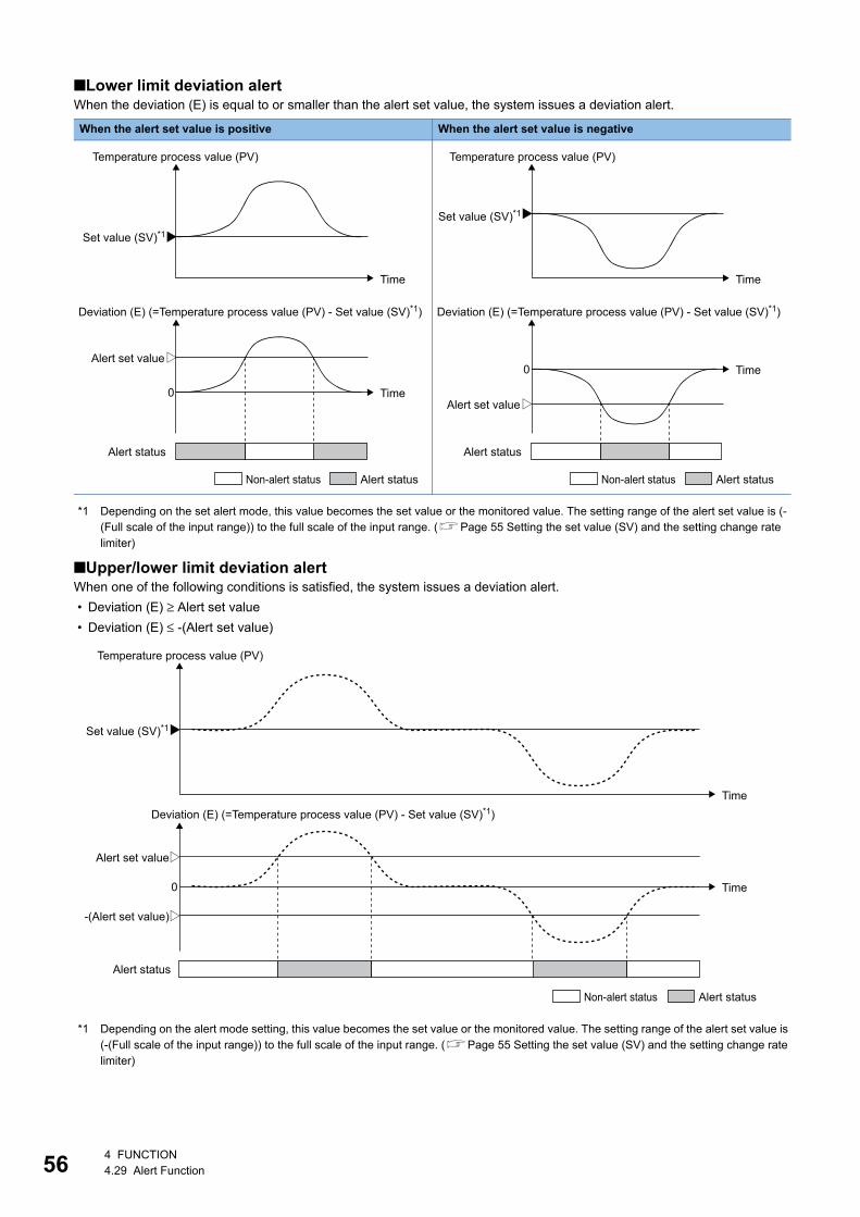
56
■Lower limit deviation alertWhen the deviation (E) is equal to or smaller than the alert set value, the system issues a deviation alert.
*1 Depending on the set alert mode, this value becomes the set value or the monitored value. The setting range of the alert set value is (-(Full scale of the input range)) to the full scale of the input range. (Page 55 Setting the set value (SV) and the setting change rate limiter)
■Upper/lower limit deviation alertWhen one of the following conditions is satisfied, the system issues a deviation alert.
• Deviation (E) ≥ Alert set value
• Deviation (E) ≤ -(Alert set value)
*1 Depending on the alert mode setting, this value becomes the set value or the monitored value. The setting range of the alert set value is (-(Full scale of the input range)) to the full scale of the input range. (Page 55 Setting the set value (SV) and the setting change rate limiter)
When the alert set value is positive When the alert set value is negative
Non-alert status Alert status
Time
Deviation (E) (=Temperature process value (PV) - Set value (SV)*1)
Alert status
0
Alert set value
Time
Temperature process value (PV)
Set value (SV)*1
Non-alert status Alert status
Time
Deviation (E) (=Temperature process value (PV) - Set value (SV)*1)
Alert status
0
Alert set value
Time
Temperature process value (PV)
Set value (SV)*1
Non-alert status Alert status
Time
Deviation (E) (=Temperature process value (PV) - Set value (SV)*1)
Alert status
0
-(Alert set value)
Alert set value
Time
Temperature process value (PV)
Set value (SV)*1
4 FUNCTION4.29 Alert Function
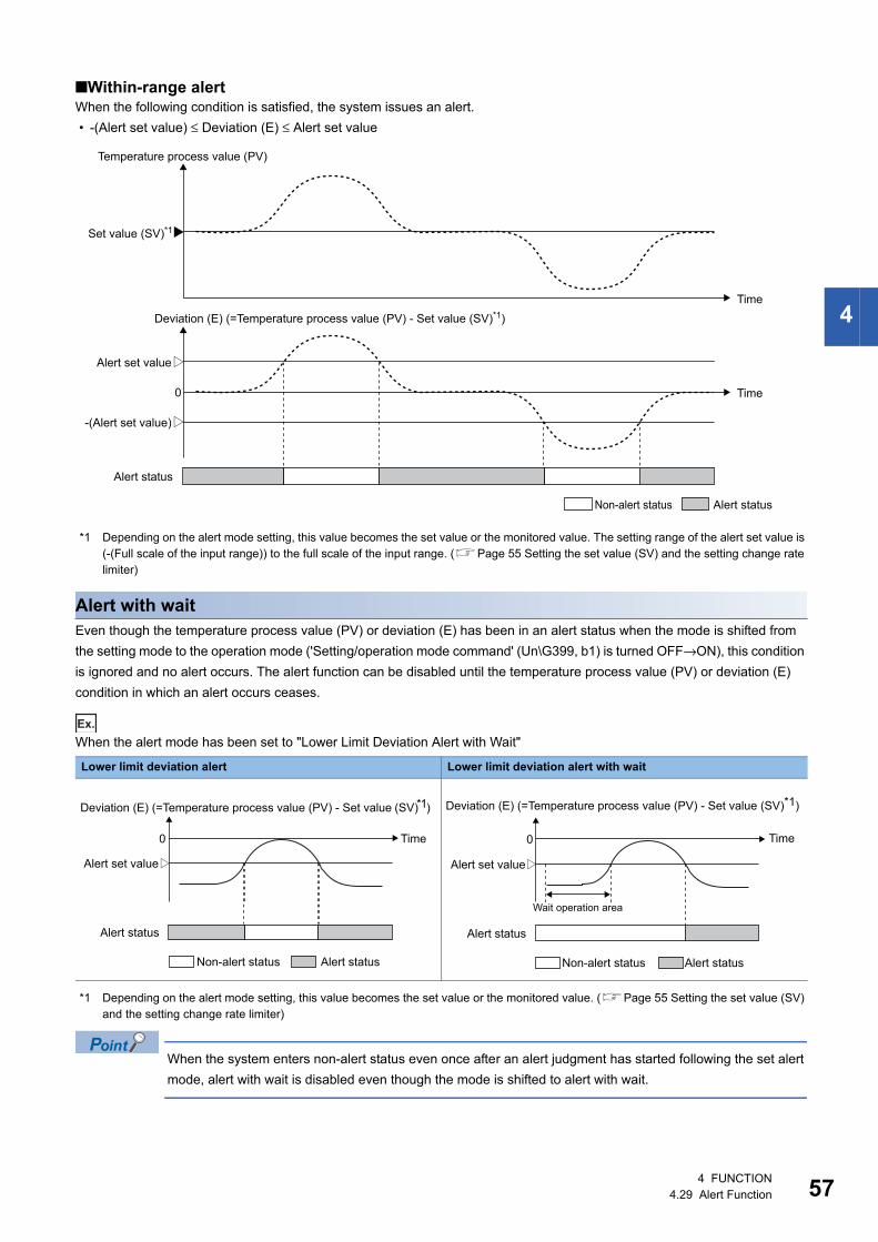
4
■Within-range alertWhen the following condition is satisfied, the system issues an alert.
• -(Alert set value) ≤ Deviation (E) ≤ Alert set value
*1 Depending on the alert mode setting, this value becomes the set value or the monitored value. The setting range of the alert set value is (-(Full scale of the input range)) to the full scale of the input range. (Page 55 Setting the set value (SV) and the setting change rate limiter)
Alert with waitEven though the temperature process value (PV) or deviation (E) has been in an alert status when the mode is shifted from
the setting mode to the operation mode ('Setting/operation mode command' (Un\G399, b1) is turned OFF→ON), this condition
is ignored and no alert occurs. The alert function can be disabled until the temperature process value (PV) or deviation (E)
condition in which an alert occurs ceases.
Ex.
When the alert mode has been set to "Lower Limit Deviation Alert with Wait"
*1 Depending on the alert mode setting, this value becomes the set value or the monitored value. (Page 55 Setting the set value (SV) and the setting change rate limiter)
When the system enters non-alert status even once after an alert judgment has started following the set alert
mode, alert with wait is disabled even though the mode is shifted to alert with wait.
Lower limit deviation alert Lower limit deviation alert with wait
Non-alert status Alert status
Time
Deviation (E) (=Temperature process value (PV) - Set value (SV)*1)
Alert status
0
-(Alert set value)
Alert set value
Time
Temperature process value (PV)
Set value (SV)*1
Non-alert status Alert status
Time
Alert status
Alert set value
Deviation (E) (=Temperature process value (PV) - Set value (SV)*1)
0
Non-alert status Alert status
Time
Alert status
Alert set value
Deviation (E) (=Temperature process value (PV) - Set value (SV)*1)
0
Wait operation area
4 FUNCTION4.29 Alert Function 57
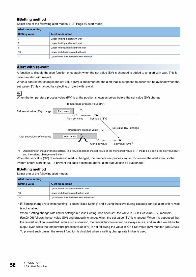
58
■Setting methodSelect one of the following alert modes. (Page 59 Alert mode)
Alert with re-waitA function to disable the alert function once again when the set value (SV) is changed is added to an alert with wait. This is
called an alert with re-wait.
When a control that changes the set value (SV) is implemented, the alert that is supposed to occur can be avoided when the
set value (SV) is changed by selecting an alert with re-wait.
Ex.
When the temperature process value (PV) is at the position shown as below before the set value (SV) change
*1 Depending on the alert mode setting, this value becomes the set value or the monitored value. (Page 55 Setting the set value (SV) and the setting change rate limiter)
When the set value (SV) of a deviation alert is changed, the temperature process value (PV) enters the alert area, so the
system enters alert status. To prevent the case described above, alert outputs can be suspended.
■Setting methodSelect one of the following alert modes.
• If "Setting change rate limiter setting" is set in "Base Setting" and if using the slave during cascade control, alert with re-wait
is not enabled.
• When "Setting change rate limiter setting" in "Base Setting" has been set, the value in 'CH1 Set value (SV) monitor'
(Un\G406) follows the set value (SV) and gradually changes when the set value (SV) is changed. When it is supposed that
the re-wait function is enabled under such a situation, the re-wait function would be always active, and an alert would not be
output even while the temperature process value (PV) is not following the value in 'CH1 Set value (SV) monitor' (Un\G406).
To prevent such cases, the re-wait function is disabled when a setting change rate limiter is used.
Alert mode setting
Setting value Alert mode name
7 Upper limit input alert with wait
8 Lower limit input alert with wait
9 Upper limit deviation alert with wait
10 Lower limit deviation alert with wait
11 Upper/lower limit deviation alert with wait
Alert mode setting
Setting value Alert mode name
12 Upper limit deviation alert with re-wait
13 Lower limit deviation alert with re-wait
14 Upper/lower limit deviation alert with re-wait
Alert set value Set value (SV)
Temperature process value (PV)
Alert areaBefore set value (SV) change
Alert set value Set value (SV)*1
Temperature process value (PV)
Alert areaAfter set value (SV) change
Set value (SV) change
4 FUNCTION4.29 Alert Function
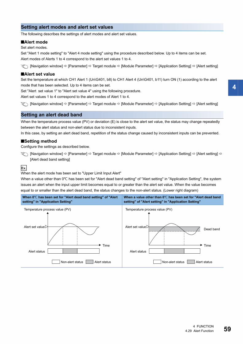
4
Setting alert modes and alert set valuesThe following describes the settings of alert modes and alert set values.
■Alert modeSet alert modes.
Set "Alert 1 mode setting" to "Alert 4 mode setting" using the procedure described below. Up to 4 items can be set.
Alert modes of Alerts 1 to 4 correspond to the alert set values 1 to 4.
[Navigation window] [Parameter] Target module [Module Parameter] [Application Setting] [Alert setting]
■Alert set valueSet the temperature at which CH1 Alert 1 (Un\G401, b8) to CH1 Alert 4 (Un\G401, b11) turn ON (1) according to the alert
mode that has been selected. Up to 4 items can be set.
Set "Alert set value 1" to "Alert set value 4" using the following procedure.
Alert set values 1 to 4 correspond to the alert modes of Alert 1 to 4.
[Navigation window] [Parameter] Target module [Module Parameter] [Application Setting] [Alert setting]
Setting an alert dead bandWhen the temperature process value (PV) or deviation (E) is close to the alert set value, the status may change repeatedly
between the alert status and non-alert status due to inconsistent inputs.
In this case, by setting an alert dead band, repetition of the status change caused by inconsistent inputs can be prevented.
■Setting methodConfigure the settings as described below.
[Navigation window] [Parameter] Target module [Module Parameter] [Application Setting] [Alert setting]
[Alert dead band setting]
Ex.
When the alert mode has been set to "Upper Limit Input Alert"
When a value other than 0 has been set for "Alert dead band setting" of "Alert setting" in "Application Setting", the system
issues an alert when the input upper limit becomes equal to or greater than the alert set value. When the value becomes
equal to or smaller than the alert dead band, the status changes to the non-alert status. (Lower right diagram)
When 0 has been set for "Alert dead band setting" of "Alert setting" in "Application Setting"
When a value other than 0 has been set for "Alert dead band setting" of "Alert setting" in "Application Setting"
Non-alert status Alert status
Time
Temperature process value (PV)
Alert status
Alert set value
Non-alert status Alert status
Time
Dead band
Temperature process value (PV)
Alert status
Alert set value
4 FUNCTION4.29 Alert Function 59
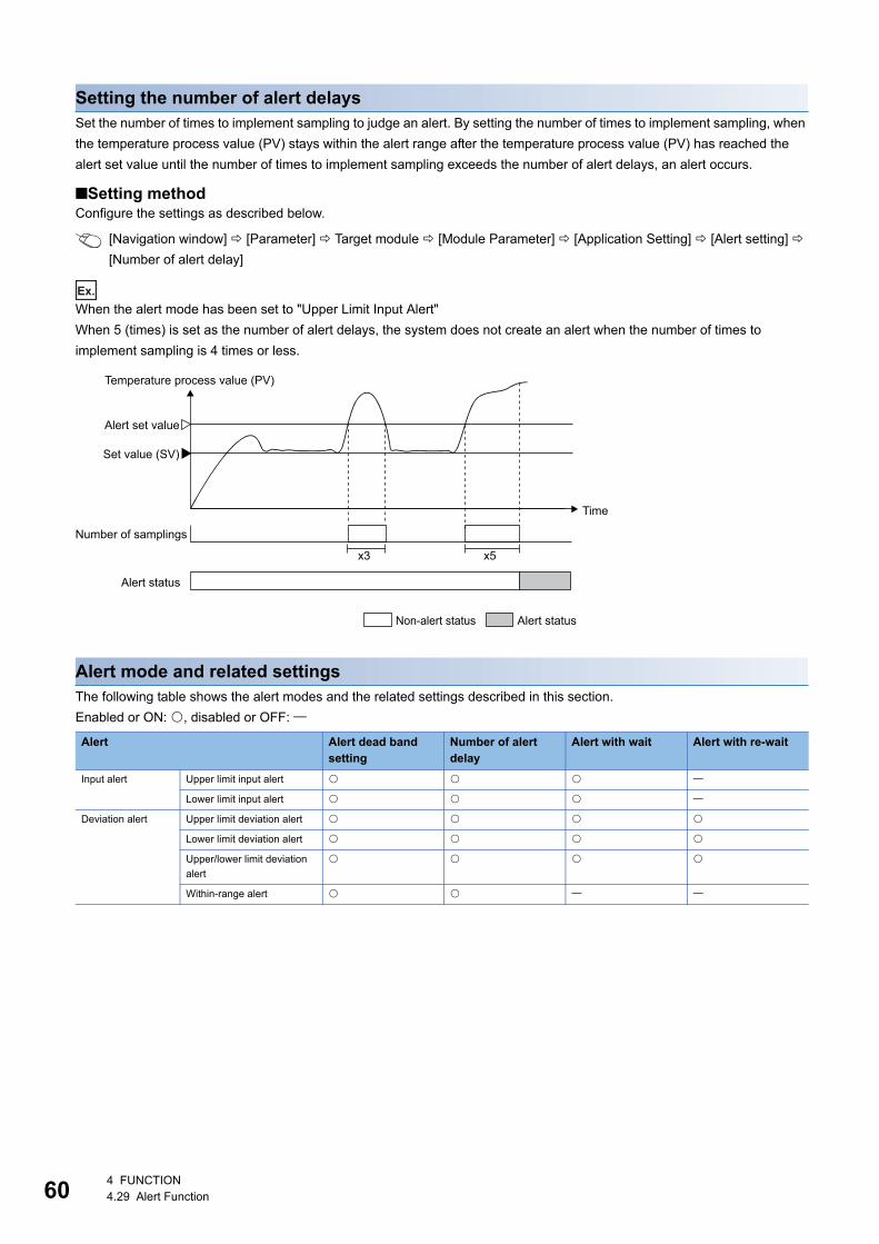
60
Setting the number of alert delaysSet the number of times to implement sampling to judge an alert. By setting the number of times to implement sampling, when
the temperature process value (PV) stays within the alert range after the temperature process value (PV) has reached the
alert set value until the number of times to implement sampling exceeds the number of alert delays, an alert occurs.
■Setting methodConfigure the settings as described below.
[Navigation window] [Parameter] Target module [Module Parameter] [Application Setting] [Alert setting]
[Number of alert delay]
Ex.
When the alert mode has been set to "Upper Limit Input Alert"
When 5 (times) is set as the number of alert delays, the system does not create an alert when the number of times to
implement sampling is 4 times or less.
Alert mode and related settingsThe following table shows the alert modes and the related settings described in this section.
Enabled or ON: , disabled or OFF:
Alert Alert dead band setting
Number of alert delay
Alert with wait Alert with re-wait
Input alert Upper limit input alert
Lower limit input alert
Deviation alert Upper limit deviation alert
Lower limit deviation alert
Upper/lower limit deviation
alert
Within-range alert
Non-alert status Alert status
Time
Temperature process value (PV)
Alert status
Number of samplings
Alert set value
x3 x5
Set value (SV)
4 FUNCTION4.29 Alert Function
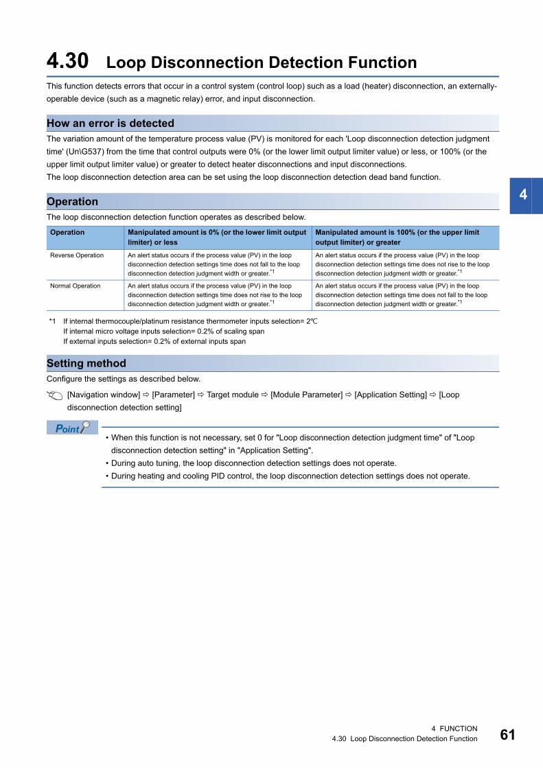
4
4.30 Loop Disconnection Detection FunctionThis function detects errors that occur in a control system (control loop) such as a load (heater) disconnection, an externally-
operable device (such as a magnetic relay) error, and input disconnection.
How an error is detectedThe variation amount of the temperature process value (PV) is monitored for each 'Loop disconnection detection judgment
time' (Un\G537) from the time that control outputs were 0% (or the lower limit output limiter value) or less, or 100% (or the
upper limit output limiter value) or greater to detect heater disconnections and input disconnections.
The loop disconnection detection area can be set using the loop disconnection detection dead band function.
OperationThe loop disconnection detection function operates as described below.
*1 If internal thermocouple/platinum resistance thermometer inputs selection= 2If internal micro voltage inputs selection= 0.2% of scaling spanIf external inputs selection= 0.2% of external inputs span
Setting methodConfigure the settings as described below.
[Navigation window] [Parameter] Target module [Module Parameter] [Application Setting] [Loop
disconnection detection setting]
• When this function is not necessary, set 0 for "Loop disconnection detection judgment time" of "Loop
disconnection detection setting" in "Application Setting".
• During auto tuning, the loop disconnection detection settings does not operate.
• During heating and cooling PID control, the loop disconnection detection settings does not operate.
Operation Manipulated amount is 0% (or the lower limit output limiter) or less
Manipulated amount is 100% (or the upper limit output limiter) or greater
Reverse Operation An alert status occurs if the process value (PV) in the loop
disconnection detection settings time does not fall to the loop
disconnection detection judgment width or greater.*1
An alert status occurs if the process value (PV) in the loop
disconnection detection settings time does not rise to the loop
disconnection detection judgment width or greater.*1
Normal Operation An alert status occurs if the process value (PV) in the loop
disconnection detection settings time does not rise to the loop
disconnection detection judgment width or greater.*1
An alert status occurs if the process value (PV) in the loop
disconnection detection settings time does not fall to the loop
disconnection detection judgment width or greater.*1
4 FUNCTION4.30 Loop Disconnection Detection Function 61
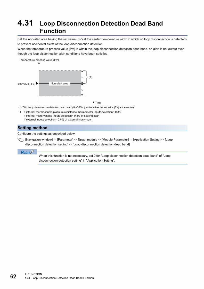
62
4.31 Loop Disconnection Detection Dead Band Function
Set the non-alert area having the set value (SV) at the center (temperature width in which no loop disconnection is detected)
to prevent accidental alerts of the loop disconnection detection.
When the temperature process value (PV) is within the loop disconnection detection dead band, an alert is not output even
though the loop disconnection alert conditions have been satisfied.
*1 If internal thermocouple/platinum resistance thermometer inputs selection= 0.8If internal micro voltage inputs selection= 0.8% of scaling spanIf external inputs selection= 0.8% of external inputs span
Setting methodConfigure the settings as described below.
[Navigation window] [Parameter] Target module [Module Parameter] [Application Setting] [Loop
disconnection detection setting] [Loop disconnection detection dead band]
When this function is not necessary, set 0 for "Loop disconnection detection dead band" of "Loop
disconnection detection setting" in "Application Setting".
(1) 'CH1 Loop disconnection detection dead band' (Un\G538) (this band has the set value (SV) at the center)*1
(1)
Time
Temperature process value (PV)
Set value (SV) Non-alert area
4 FUNCTION4.31 Loop Disconnection Detection Dead Band Function
4
4.32 Heater Disconnection Detection FunctionWhen a transistor output is ON, this function checks whether or not a heater has a disconnection using the Heater current
process value (load current value detected by a current sensor (CT)). This function compares the heater current process
value and the heater disconnection alert current value. When the Heater current process value becomes equal to or smaller
than the heater disconnection alert current value, the heater is regarded as having a disconnection. However, when the
transistor-output ON time is 220 ms or less, no heater disconnection is detected. (CH1 Heater disconnection detection
(Un\G401, b12) remains OFF.)
The timing when an alert is output is described below.
• 500 ms×n
n = Value set for "Heater disconnection/output OFF-time current error detection delay count" of "Loop disconnection detection
setting" in "Application Setting"
When the heater disconnection status lasts longer than the time described above, the following operations are implemented.
• 'CH1 alert ON flag' (Un\G398, b12) turns ON (1).
• 'CH1 Heater disconnection detection' (Un\G401, b12) turns ON (1).
• CH heater disconnection detection (alarm code: 088) is stored in 'Latest alarm code' (Un\G3).
Setting methodConfigure the settings as described below.
1. Set the judgment value for heater disconnection detection in "Heater disconnection alert settings" in "Loop disconnection
detection settings" in "Application Setting".
[Navigation window] [Parameter] Target module [Module Parameter] [Application Setting] [Heater
disconnection detection setting]
2. Set how many times heater disconnections are detected successively to regard the heater as disconnected for "Heater
disconnection/output OFF-time current error detection delay count" of "Heater disconnection detection setting" in
"Application Setting".
4.33 Output OFF-time Current Error Detection FunctionTransistor output errors can be detected using this function. A current sensor (CT) for heater disconnection detection is used
to check for errors of when transistor outputs are OFF.
A Heater current process value and the heater disconnection alert current value are compared. If the Heater current process
value is larger than the heater disconnection alert current value, an output OFF-time current error occurs.
Detection of output OFF-time current errors is implemented every 500 ms. When the OFF time of a transistor output has been
set as 220 ms below, output OFF-time current errors are not detected. (CH1 Output OFF-time current error (Un\G401, b14)
remains OFF (0).)
The timing when an alert is output is described below.
• 500 ms×n
n = Value set for "Heater disconnection/output OFF-time current error detection delay count" of "Loop disconnection detection
setting" in "Application Setting"
When the output OFF-time current error status lasts longer than the time described above, the following operations are
implemented.
• 'CH1 alert ON flag' (Un\G398, b12) turns ON (1).
• 'CH1 Output OFF-time current error' (Un\G401, b14) turns ON (1).
• Current error detection when CH outputs are OFF (alarm code: 08A) is stored in 'Latest alarm code' (Un\G3).
4 FUNCTION4.32 Heater Disconnection Detection Function 63
64
Setting methodConfigure the settings as described below.
1. Set the judgment value for current error detection when outputs are OFF in "Heater disconnection alert settings" in"Loop
disconnection detection settings" in "Application Setting".
[Navigation window] [Parameter] Target module [Module Parameter] [Application Setting] [Heater
disconnection detection setting]
2. Set how many times current errors while outputs are OFF are detected successively to regard a current error while
outputs are OFF as having occurred in "Heater disconnection/output OFF-time current error detection delay count" of
"Heater disconnection detection setting" in "Application Setting".
4.34 Buffer Memory Data Backup FunctionThis function backs up data in buffer memory areas to the non-volatile memory.
The backed up data is transferred from the non-volatile memory to the buffer memory when the power is turned OFF→ON or
the CPU module is reset. Consequently, when the power supply is turned OFF→ON and the CPU module is reset,
temperatures can be adjusted even if no data has been written.
Target buffer memoryRefer to the list of buffer memory allocations. (Page 99 List of buffer memory addresses)
See below for the functions whose PID constants are automatically backed up after the auto tuning.
Page 99 List of buffer memory addresses
To write data to the non-volatile memory, turn OFF and ON 'Setting value backup command' (Un\G399, b8).
When writing the data to the non-volatile memory is completed, 'Setting value backup completion flag' (Un\G398, b8) turns
ON.
If writing the data to the non-volatile memory is not completed successfully, 'Setting value backup failure flag' (Un\G398, b10)
turns ON.
■Setting changeChange the settings of the buffer memory areas while 'Setting value backup completion flag' (Un\G398, b8) is OFF.
■Reading data from the non-volatile memoryReading is enabled when the power supply is turned OFF→ON and the CPU module is reset.
■Precautions following implementation of the set value backup functionWhen the power supply is turned OFF→ON and the CPU module is reset after this function is implemented, the data
transferred to buffer memory is overwritten by the GX Works3 parameter settings.
To use the set values stored as the backup data of the initial settings of the module, implement one of the following actions.
• Do not set GX Works3 parameters
• When configuring the parameter setting of GX Works3, correct the set values of the parameters to the ones stored as
backup data, and write the parameters to the CPU module
Read
Temperature control moduleCPU module 1. "Set value backup command"
(Un\G399, b8): ON (Write command)
3. "Set value backup completion flag"(Un\G398, b8): ON (complete)
2. Write
Non-volatile memory
When power is turned OFF ONDuring STOP RUNDuring reset
Buffer memory data
4 FUNCTION4.34 Buffer Memory Data Backup Function
4
4.35 Default FunctionThe data type initializes the "settings" buffer memory.
For the types of buffer memory, refer to the following.
Page 99 List of buffer memory addresses
Setting methodSet in the following buffer memory area.
• Default setting registration command (Un\G399, b9) (Page 127 Default setting registration command (b9))
Precautions
• In normal mode, control mode selection and auto settings during input range changes, output signal are not initialized.
• Not initialized during control or implementation of the buffer memory data backup function.
4.36 Error History FunctionThe errors or alarms that occurred in the temperature control module are stored in the buffer memory as history. A maximum
16 of both errors and alarms can be stored.
OperationWhen errors occur, error codes and error times of the errors are stored in 'Error history No.1' (Un\G3600 to Un\G3609) in
order.
When alarms occur, alarm codes and alarm times of the alarms are stored in 'Alarm history No.1' (Un\G3760 to Un\G3769) in
order.
• Error code allocation details
• Alarm code allocation details
b15 to tob8 b7 b0
…
Error code
System area
First 2 digits of date Last 2 digits of dateMonth DayTime Minute
SecondMillisecond (upper)
Day of the weekMillisecond (lower)
Un\G3600
Un\G3604Un\G3603Un\G3602Un\G3601
Un\G3605Un\G3606
Un\G3609
b15 to tob8 b7 b0
…
Alarm code
System area
First 2 digits of date Last 2 digits of dateMonth DayTime Minute
SecondMillisecond (upper)
Day of the weekMillisecond (lower)
Un\G3760
Un\G3764Un\G3763Un\G3762Un\G3761
Un\G3765Un\G3766
Un\G3769
4 FUNCTION4.35 Default Function 65
66
Ex.
Storage example of error history and alarm history data
*1 Value stored when an error occurs at 12:34:56.789 on Saturday, January 31, 2015
The start address of the error history where the latest error has been stored can be checked in 'Latest address of error history'
(Un\G2).
The start address of the alarm history where the latest alarm has been stored can be checked in 'Latest address of alarm
history' (Un\G4).
Ex.
When the third error occurred
The third error is stored in Error history No. 3 and 3620 (the start address of Error history No.3) is stored in 'Latest address of
error history' (Un\G2).
Item Stored contents Storage example*1
First two digits of the year/last two digits
of the year
Stored in BCD code. 2015H
Month/day 131H
Hour/minute 1234H
Second 56H
Day of the week One of the following values is stored in BCD code.
Sunday: 0, Monday: 1, Tuesday: 2, Wednesday: 3
Thursday: 4, Friday: 5, Saturday: 6
6H
Millisecond (upper) Stored in BCD code. 7H
Millisecond (lower) 89H
Error history No. 1
Error history No. 2
Error history No. 3
Error history No. 16
(Open)
(Open)
Latest
Un\G3600
Un\G3610
Un\G3620
Un\G3750
1st error
2nd error
3rd error
"Latest address of error history"(Un\G2): 3620
4 FUNCTION4.36 Error History Function
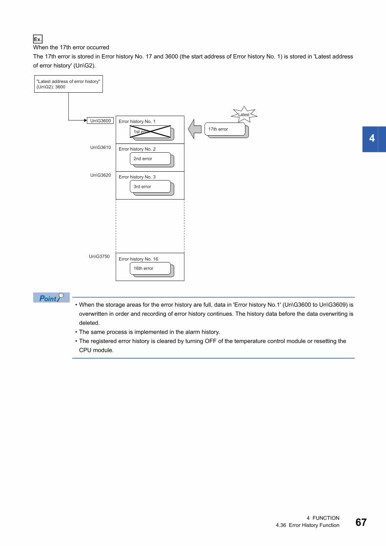
4
Ex.
When the 17th error occurred
The 17th error is stored in Error history No. 17 and 3600 (the start address of Error history No. 1) is stored in 'Latest address
of error history' (Un\G2).
• When the storage areas for the error history are full, data in 'Error history No.1' (Un\G3600 to Un\G3609) is
overwritten in order and recording of error history continues. The history data before the data overwriting is
deleted.
• The same process is implemented in the alarm history.
• The registered error history is cleared by turning OFF of the temperature control module or resetting the
CPU module.
Error history No. 1
Error history No. 2
Error history No. 3
Error history No. 16
LatestUn\G3600
Un\G3610
Un\G3620
Un\G3750
1st error
2nd error
17th error
"Latest address of error history"(Un\G2): 3600
3rd error
16th error
4 FUNCTION4.36 Error History Function 67
68
4.37 FX3 Allocation Mode FunctionThe temperature control module buffer memory addresses can be arranged in the same way as for FX3U-4LC.
Sequence programs proven with the FX3U-4LC can be used.
OperationIn FX3 allocation mode, broad program corrections are not required during FX3 program appropriation as the buffer memory
allocations are the same as for FX3U-4LC.
Further, in FX3 allocation mode, the temperature adjustment settings can be set from the parameters.
Setting methodConfigure the settings as described below.
1. When adding a new module, select a module whose name has "(FX3)" after its module model name.
[Navigation] [Parameter] [Module Information] Right-click [Add New Module]
2. Set parameters in the same way as in normal mode.
3. Write the parameters to the module, and then either reset or turn OFF→ON the power supply.
• It is not possible to switch between normal mode and FX3 allocation mode during operations.
• "Temperature control trace" in the module tools is not compatible with FX3 allocation mode.
4 FUNCTION4.37 FX3 Allocation Mode Function
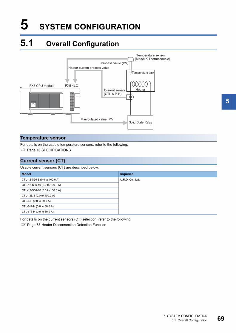
5
5 SYSTEM CONFIGURATION
5.1 Overall Configuration
Temperature sensorFor details on the usable temperature sensors, refer to the following.
Page 16 SPECIFICATIONS
Current sensor (CT)Usable current sensors (CT) are described below.
For details on the current sensors (CT) selection, refer to the following.
Page 63 Heater Disconnection Detection Function
Model Inquiries
CTL-12-S36-8 (0.0 to 100.0 A) U.R.D. Co., Ltd.
CTL-12-S36-10 (0.0 to 100.0 A)
CTL-12-S56-10 (0.0 to 100.0 A)
CTL-12L-8 (0.0 to 100.0 A)
CTL-6-P (0.0 to 30.0 A)
CTL-6-P-H (0.0 to 30.0 A)
CTL-6-S-H (0.0 to 30.0 A)
Process value (PV)
Manipulated value (MV)
Temperature sensor(Model K Thermocouple)
Temperature tank
Solid State Relay
Current sensor(CTL-6-P-H)
Heater
Heater current process value
FX5 CPU module FX5-4LC
5 SYSTEM CONFIGURATION5.1 Overall Configuration 69
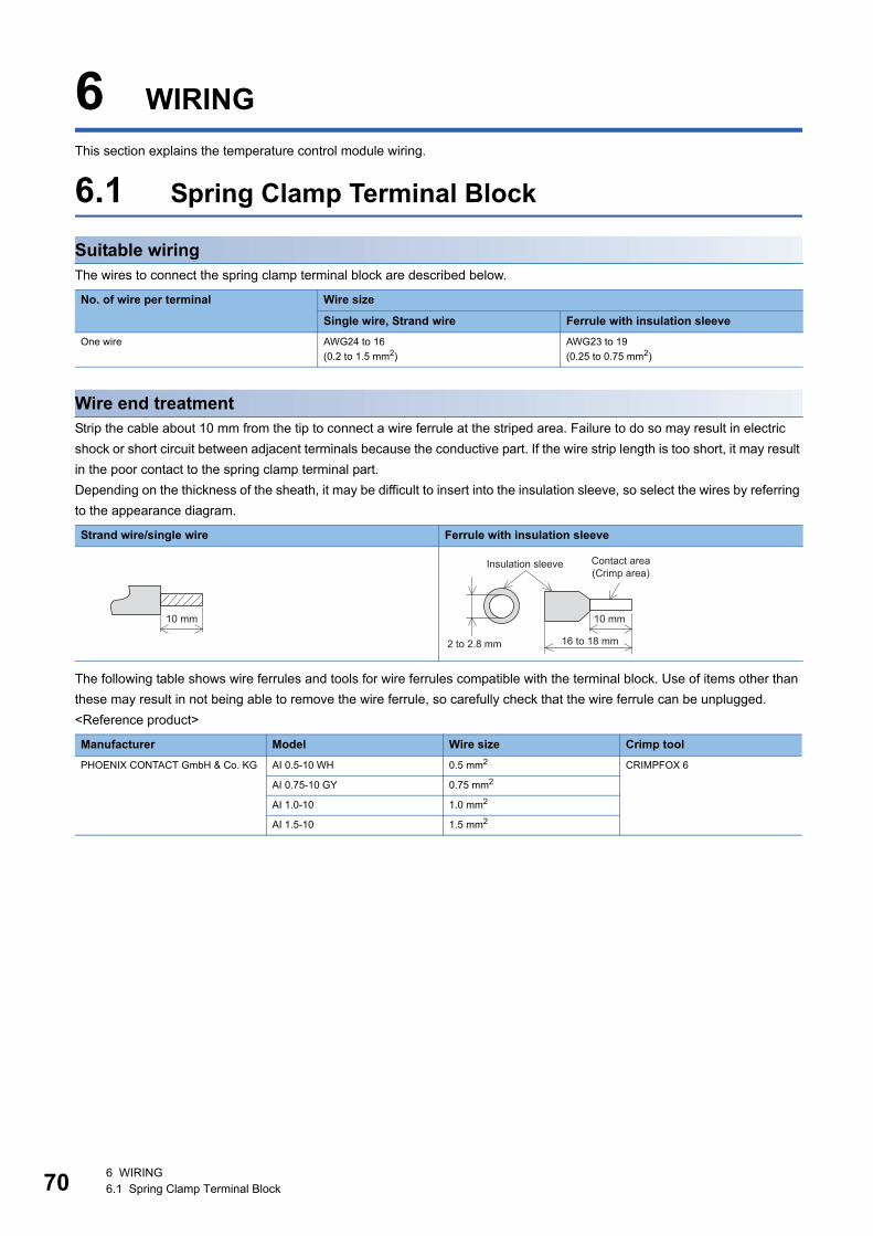
70
6 WIRING
This section explains the temperature control module wiring.
6.1 Spring Clamp Terminal Block
Suitable wiringThe wires to connect the spring clamp terminal block are described below.
Wire end treatmentStrip the cable about 10 mm from the tip to connect a wire ferrule at the striped area. Failure to do so may result in electric
shock or short circuit between adjacent terminals because the conductive part. If the wire strip length is too short, it may result
in the poor contact to the spring clamp terminal part.
Depending on the thickness of the sheath, it may be difficult to insert into the insulation sleeve, so select the wires by referring
to the appearance diagram.
The following table shows wire ferrules and tools for wire ferrules compatible with the terminal block. Use of items other than
these may result in not being able to remove the wire ferrule, so carefully check that the wire ferrule can be unplugged.
<Reference product>
No. of wire per terminal Wire size
Single wire, Strand wire Ferrule with insulation sleeve
One wire AWG24 to 16
(0.2 to 1.5 mm2)
AWG23 to 19
(0.25 to 0.75 mm2)
Strand wire/single wire Ferrule with insulation sleeve
Manufacturer Model Wire size Crimp tool
PHOENIX CONTACT GmbH & Co. KG AI 0.5-10 WH 0.5 mm2 CRIMPFOX 6
AI 0.75-10 GY 0.75 mm2
AI 1.0-10 1.0 mm2
AI 1.5-10 1.5 mm2
10 mm 10 mm
Contact area(Crimp area)
16 to 18 mm2 to 2.8 mm
Insulation sleeve
6 WIRING6.1 Spring Clamp Terminal Block
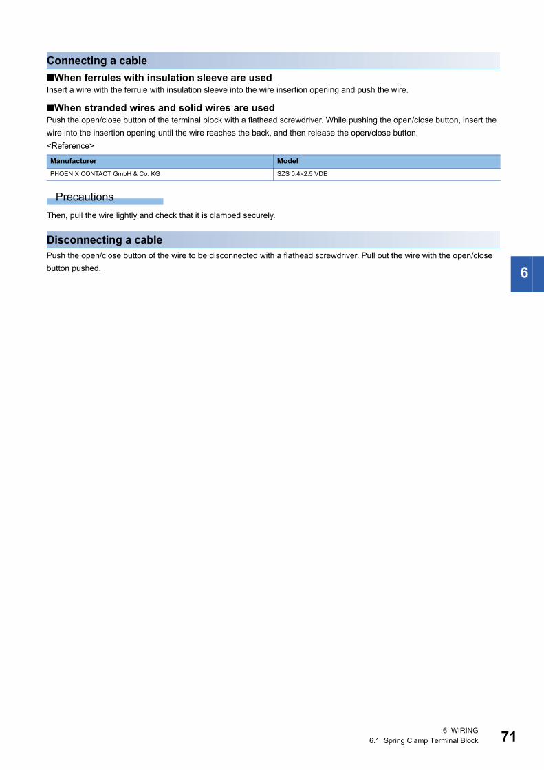
6
Connecting a cable
■When ferrules with insulation sleeve are usedInsert a wire with the ferrule with insulation sleeve into the wire insertion opening and push the wire.
■When stranded wires and solid wires are usedPush the open/close button of the terminal block with a flathead screwdriver. While pushing the open/close button, insert the
wire into the insertion opening until the wire reaches the back, and then release the open/close button.
<Reference>
Precautions
Then, pull the wire lightly and check that it is clamped securely.
Disconnecting a cablePush the open/close button of the wire to be disconnected with a flathead screwdriver. Pull out the wire with the open/close
button pushed.
Manufacturer Model
PHOENIX CONTACT GmbH & Co. KG SZS 0.4×2.5 VDE
6 WIRING6.1 Spring Clamp Terminal Block 71
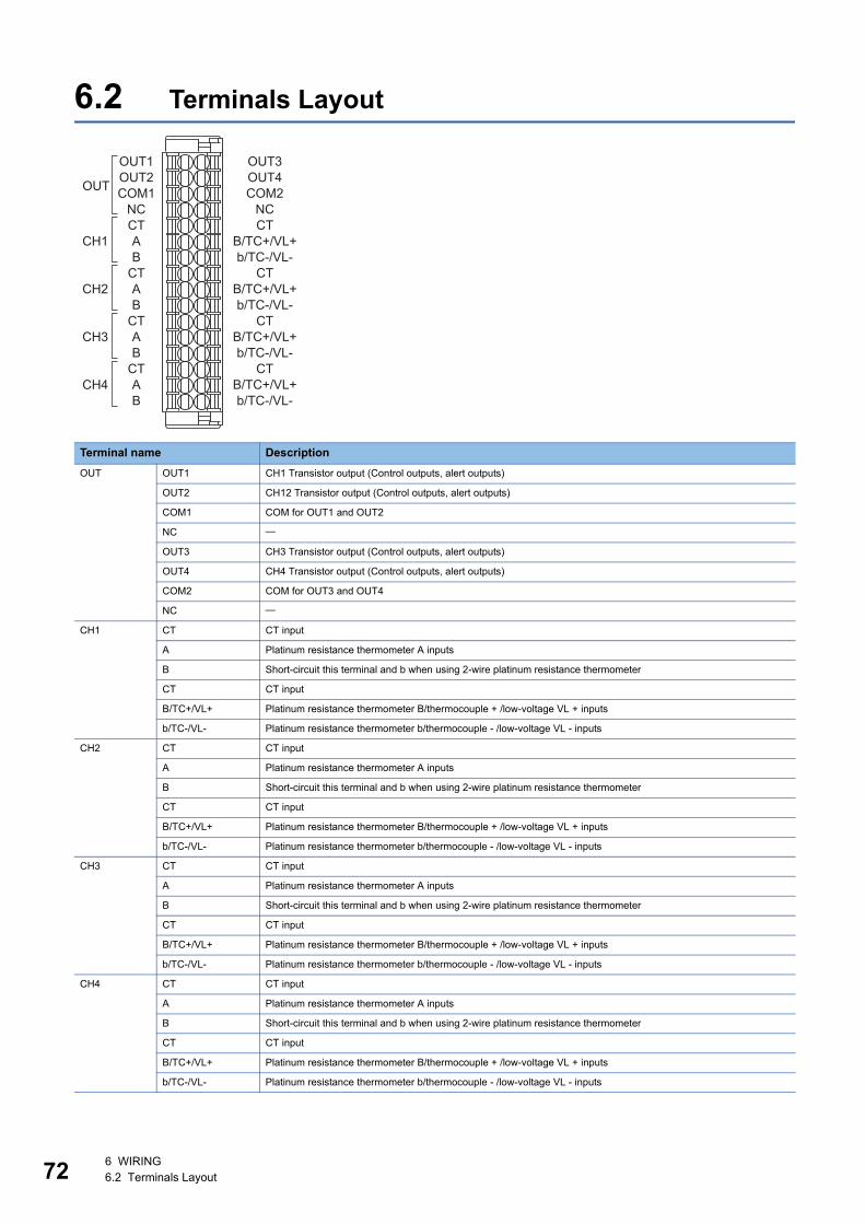
72
6.2 Terminals Layout
Terminal name Description
OUT OUT1 CH1 Transistor output (Control outputs, alert outputs)
OUT2 CH12 Transistor output (Control outputs, alert outputs)
COM1 COM for OUT1 and OUT2
NC
OUT3 CH3 Transistor output (Control outputs, alert outputs)
OUT4 CH4 Transistor output (Control outputs, alert outputs)
COM2 COM for OUT3 and OUT4
NC
CH1 CT CT input
A Platinum resistance thermometer A inputs
B Short-circuit this terminal and b when using 2-wire platinum resistance thermometer
CT CT input
B/TC+/VL+ Platinum resistance thermometer B/thermocouple + /low-voltage VL + inputs
b/TC-/VL- Platinum resistance thermometer b/thermocouple - /low-voltage VL - inputs
CH2 CT CT input
A Platinum resistance thermometer A inputs
B Short-circuit this terminal and b when using 2-wire platinum resistance thermometer
CT CT input
B/TC+/VL+ Platinum resistance thermometer B/thermocouple + /low-voltage VL + inputs
b/TC-/VL- Platinum resistance thermometer b/thermocouple - /low-voltage VL - inputs
CH3 CT CT input
A Platinum resistance thermometer A inputs
B Short-circuit this terminal and b when using 2-wire platinum resistance thermometer
CT CT input
B/TC+/VL+ Platinum resistance thermometer B/thermocouple + /low-voltage VL + inputs
b/TC-/VL- Platinum resistance thermometer b/thermocouple - /low-voltage VL - inputs
CH4 CT CT input
A Platinum resistance thermometer A inputs
B Short-circuit this terminal and b when using 2-wire platinum resistance thermometer
CT CT input
B/TC+/VL+ Platinum resistance thermometer B/thermocouple + /low-voltage VL + inputs
b/TC-/VL- Platinum resistance thermometer b/thermocouple - /low-voltage VL - inputs
OUT1OUT2COM1
NCCTACH1
OUT
CH2
CH3
CH4
BCTAB
CTAB
CTAB
OUT3OUT4COM2
NCCT
B/TC+/VL+b/TC-/VL-
CTB/TC+/VL+b/TC-/VL-
CTB/TC+/VL+b/TC-/VL-
CTB/TC+/VL+b/TC-/VL-
6 WIRING6.2 Terminals Layout
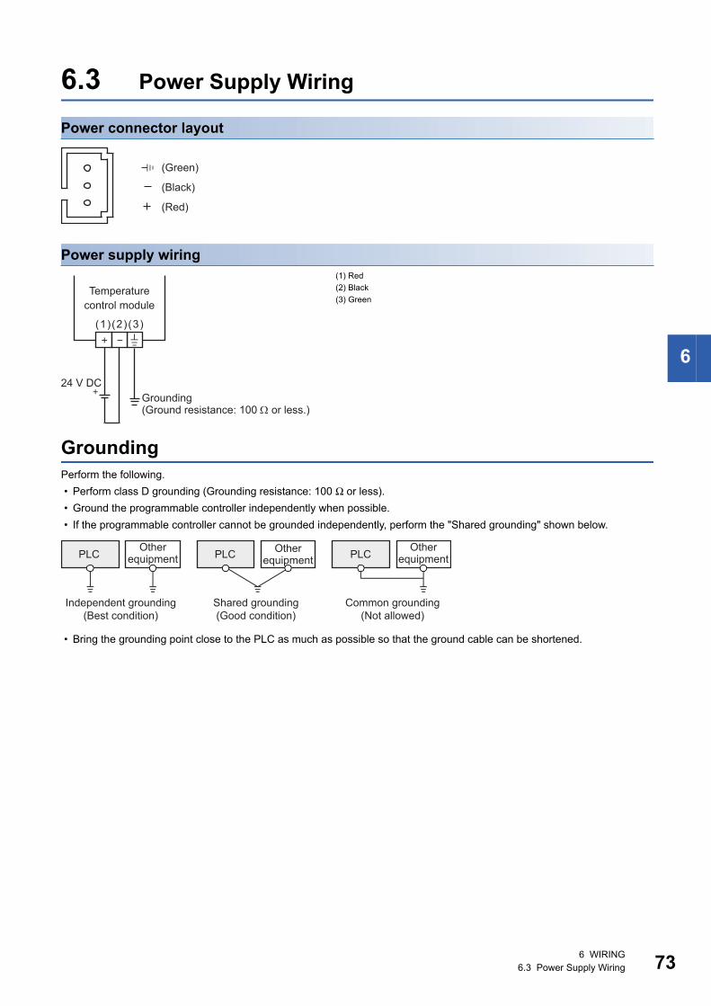
6
6.3 Power Supply Wiring
Power connector layout
Power supply wiring
GroundingPerform the following.
• Perform class D grounding (Grounding resistance: 100 Ω or less).
• Ground the programmable controller independently when possible.
• If the programmable controller cannot be grounded independently, perform the "Shared grounding" shown below.
• Bring the grounding point close to the PLC as much as possible so that the ground cable can be shortened.
(1) Red
(2) Black
(3) Green
(Green)
(Black)
(Red)
Grounding(Ground resistance: 100 or less.)
24 V DC
(1)(2)(3)
Temperature control module
PLC PLC PLCOther
equipmentOther
equipmentOther
equipment
Shared grounding(Good condition)
Common grounding(Not allowed)
Independent grounding(Best condition)
6 WIRING6.3 Power Supply Wiring 73
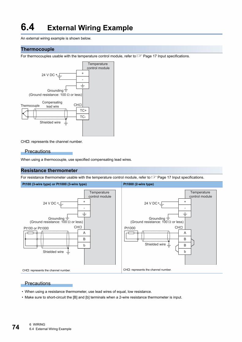
74
6.4 External Wiring ExampleAn external wiring example is shown below.
ThermocoupleFor thermocouples usable with the temperature control module, refer toPage 17 Input specifications.
CH: represents the channel number.
Precautions
When using a thermocouple, use specified compensating lead wires.
Resistance thermometerFor resistance thermometer usable with the temperature control module, refer toPage 17 Input specifications.
Precautions
• When using a resistance thermometer, use lead wires of equal, low resistance.
• Make sure to short-circuit the [B] and [b] terminals when a 2-wire resistance thermometer is input.
Pt100 (3-wire type) or Pt1000 (3-wire type) Pt1000 (2-wire type)
CH: represents the channel number. CH: represents the channel number.
24 V DC
Temperature control module
+
-
Grounding(Ground resistance: 100 or less)
CH
TC-
TC+Thermocouple
Compensating lead wire
Shielded wire
24 V DC
Temperature control module
+
-
Grounding(Ground resistance: 100 or less)
B
A
b
Shielded wire
Pt100 or Pt1000 CH
24 V DC
Temperature control module
+
-
Grounding(Ground resistance: 100 or less)
B
A
B
b
Shielded wire
Pt1000 CH
6 WIRING6.4 External Wiring Example
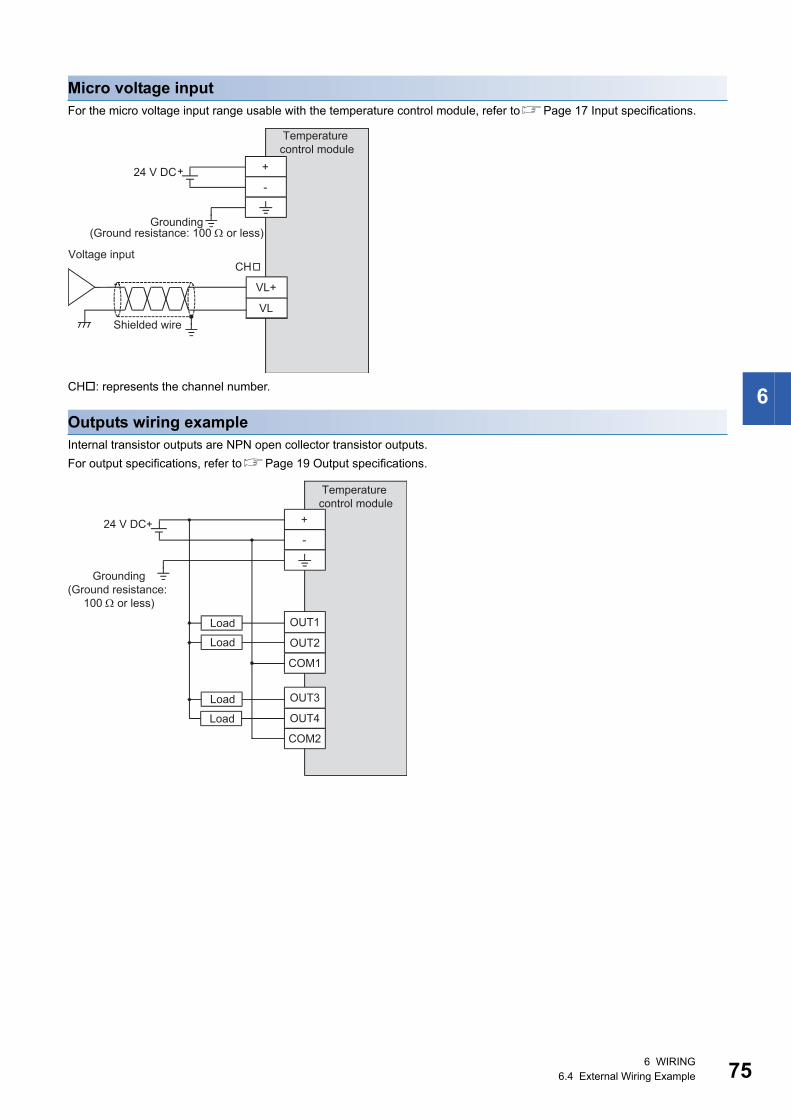
6
Micro voltage inputFor the micro voltage input range usable with the temperature control module, refer toPage 17 Input specifications.
CH: represents the channel number.
Outputs wiring exampleInternal transistor outputs are NPN open collector transistor outputs.
For output specifications, refer toPage 19 Output specifications.
24 V DC
Temperature control module
+
-
Grounding(Ground resistance: 100 or less)
VL
VL+
Shielded wire
Voltage inputCH
24 V DC
Temperature control module
+
-
Grounding(Ground resistance:
100 or less)
OUT2
OUT1
COM1
OUT4
OUT3
COM2
Load
Load
Load
Load
6 WIRING6.4 External Wiring Example 75
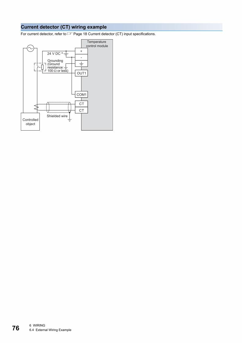
76
Current detector (CT) wiring exampleFor current detector, refer toPage 18 Current detector (CT) input specifications.
Temperature control module
+
-24 V DC
Grounding(Ground resistance:100 or less)
Shielded wireControlled
object
CT
CT
COM1
OUT1
6 WIRING6.4 External Wiring Example
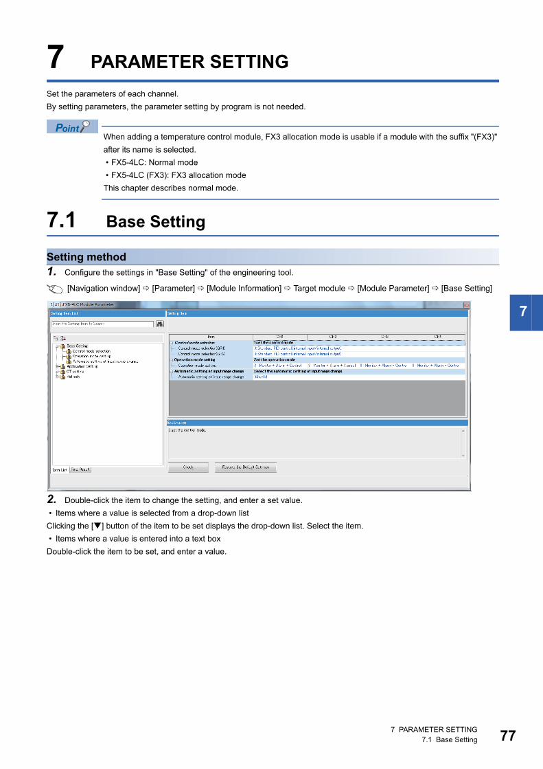
7
7 PARAMETER SETTING
Set the parameters of each channel.
By setting parameters, the parameter setting by program is not needed.
When adding a temperature control module, FX3 allocation mode is usable if a module with the suffix "(FX3)"
after its name is selected.
• FX5-4LC: Normal mode
• FX5-4LC (FX3): FX3 allocation mode
This chapter describes normal mode.
7.1 Base Setting
Setting method1. Configure the settings in "Base Setting" of the engineering tool.
[Navigation window] [Parameter] [Module Information] Target module [Module Parameter] [Base Setting]
2. Double-click the item to change the setting, and enter a set value.
• Items where a value is selected from a drop-down list
Clicking the [] button of the item to be set displays the drop-down list. Select the item.
• Items where a value is entered into a text box
Double-click the item to be set, and enter a value.
7 PARAMETER SETTING7.1 Base Setting 77
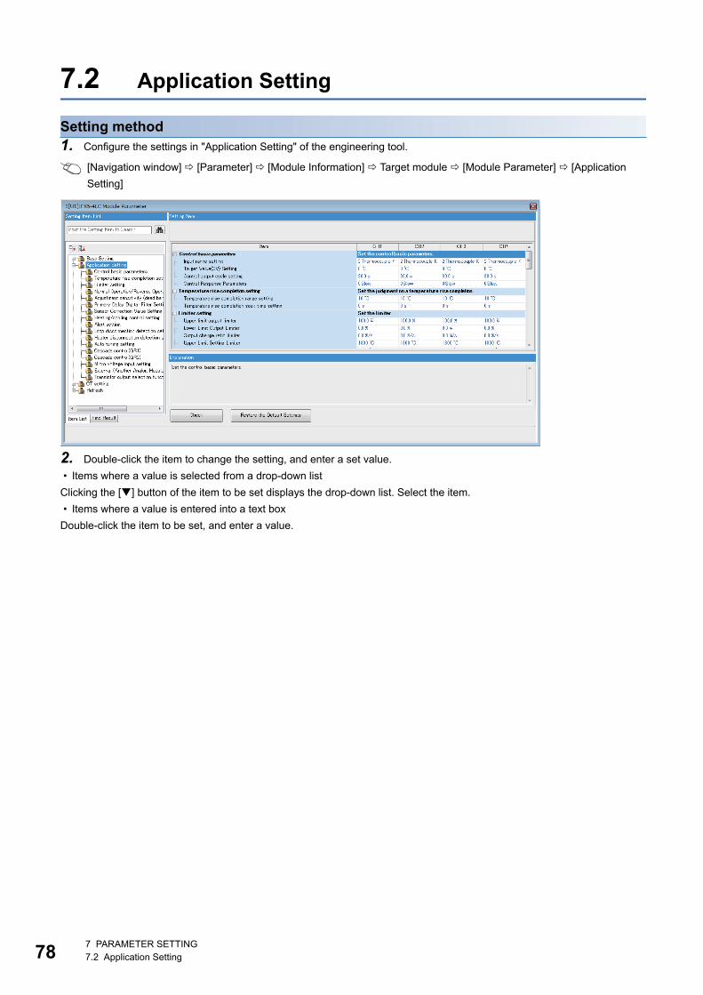
78
7.2 Application Setting
Setting method1. Configure the settings in "Application Setting" of the engineering tool.
[Navigation window] [Parameter] [Module Information] Target module [Module Parameter] [Application
Setting]
2. Double-click the item to change the setting, and enter a set value.
• Items where a value is selected from a drop-down list
Clicking the [] button of the item to be set displays the drop-down list. Select the item.
• Items where a value is entered into a text box
Double-click the item to be set, and enter a value.
7 PARAMETER SETTING7.2 Application Setting
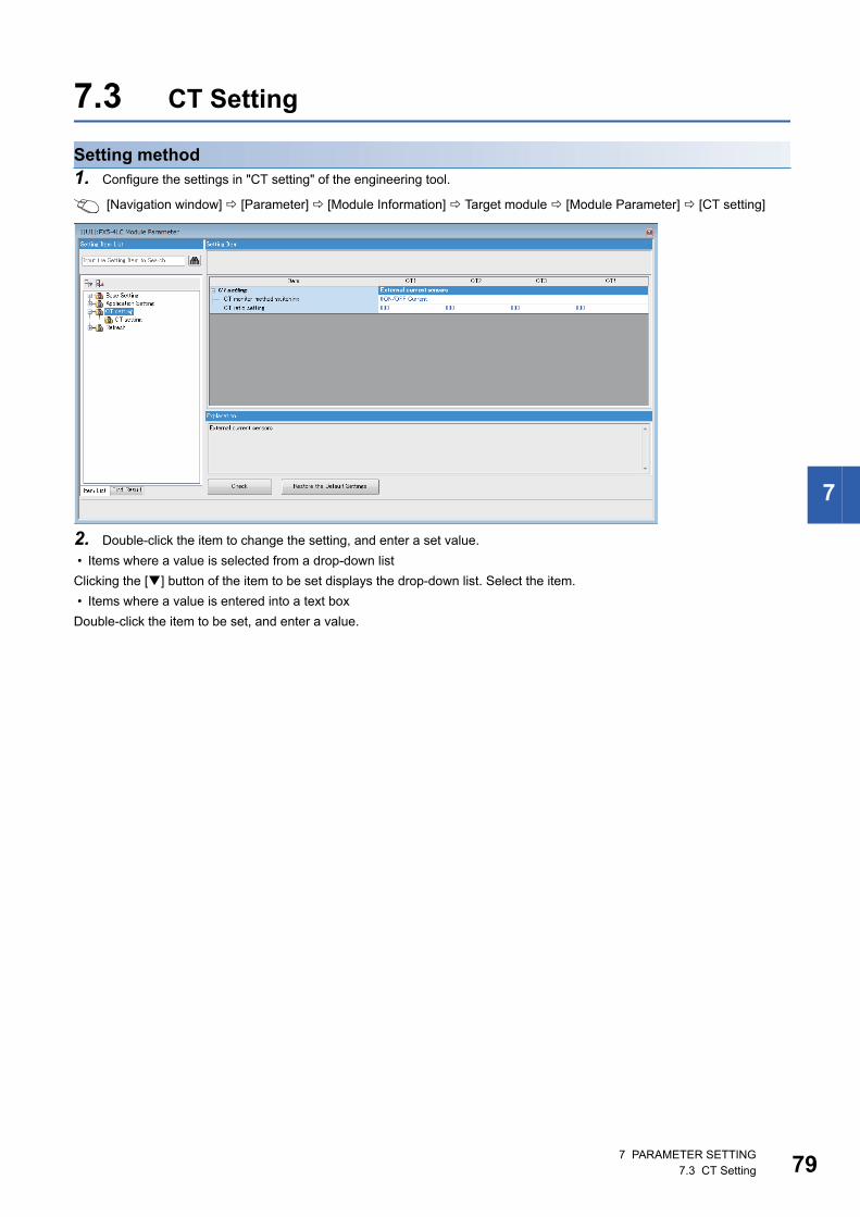
7
7.3 CT Setting
Setting method1. Configure the settings in "CT setting" of the engineering tool.
[Navigation window] [Parameter] [Module Information] Target module [Module Parameter] [CT setting]
2. Double-click the item to change the setting, and enter a set value.
• Items where a value is selected from a drop-down list
Clicking the [] button of the item to be set displays the drop-down list. Select the item.
• Items where a value is entered into a text box
Double-click the item to be set, and enter a value.
7 PARAMETER SETTING7.3 CT Setting 79
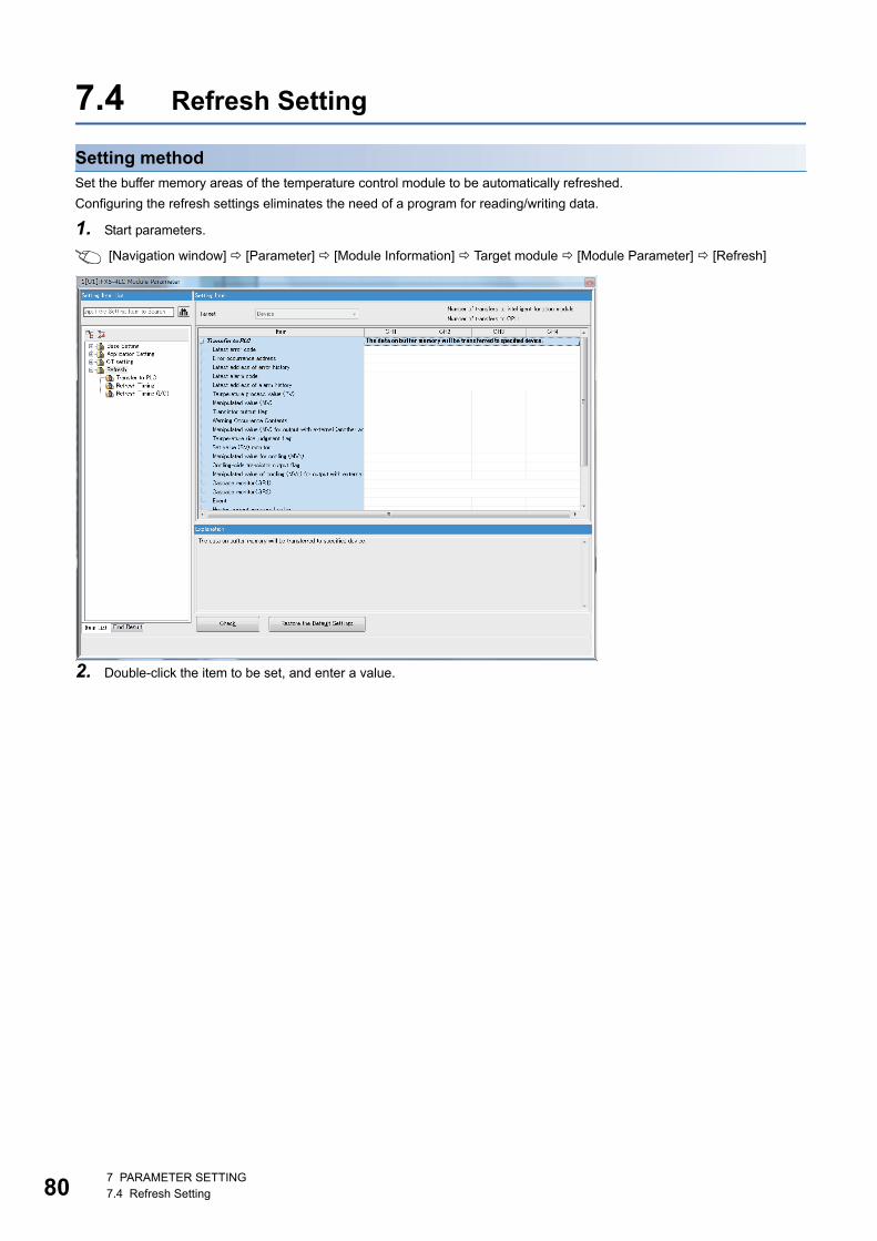
80
7.4 Refresh Setting
Setting methodSet the buffer memory areas of the temperature control module to be automatically refreshed.
Configuring the refresh settings eliminates the need of a program for reading/writing data.
1. Start parameters.
[Navigation window] [Parameter] [Module Information] Target module [Module Parameter] [Refresh]
2. Double-click the item to be set, and enter a value.
7 PARAMETER SETTING7.4 Refresh Setting
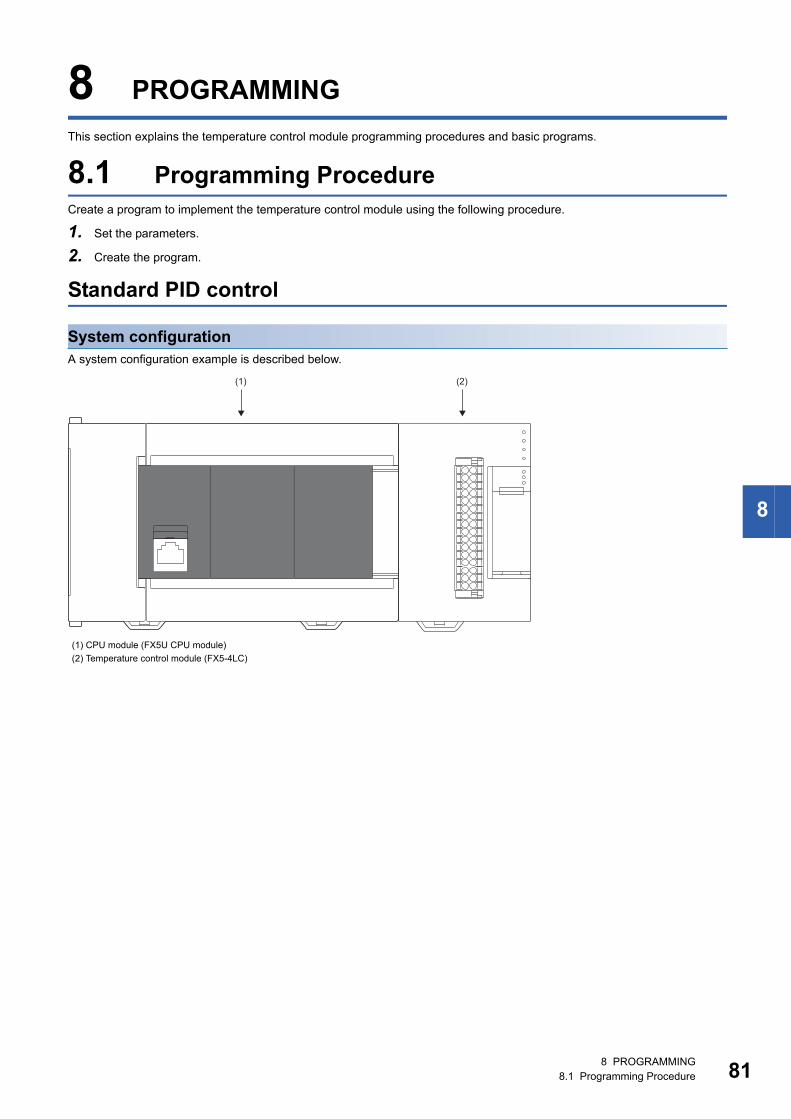
8
8 PROGRAMMING
This section explains the temperature control module programming procedures and basic programs.
8.1 Programming ProcedureCreate a program to implement the temperature control module using the following procedure.
1. Set the parameters.
2. Create the program.
Standard PID control
System configurationA system configuration example is described below.
(1) CPU module (FX5U CPU module)
(2) Temperature control module (FX5-4LC)
(1) (2)
8 PROGRAMMING8.1 Programming Procedure 81
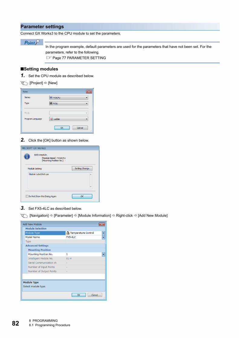
82
Parameter settingsConnect GX Works3 to the CPU module to set the parameters.
In the program example, default parameters are used for the parameters that have not been set. For the
parameters, refer to the following.
Page 77 PARAMETER SETTING
■Setting modules
1. Set the CPU module as described below.
[Project] [New]
2. Click the [OK] button as shown below.
3. Set FX5-4LC as described below.
[Navigation] [Parameter] [Module Information] Right-click [Add New Module]
8 PROGRAMMING8.1 Programming Procedure
8
4. Click the [OK] button as shown below.
■Setting temperature control module parameters
1. Set the "Base Setting" contents as described below.
[Navigation window] [Parameter] [Module Information] [FX5-4LC] [Module Parameter] [Base Setting]
8 PROGRAMMING8.1 Programming Procedure 83
84
2. Set the "Application Setting" contents as described below.
[Navigation window] [Parameter] [Module Information] [FX5-4LC] [Module Parameter] [Application Setting]
• "Control basic parameters"
Set the CH1 "Target Value (SV) Setting" as shown in the diagram below.
• "Limiter setting"
Set the CH1 "Upper Limit Setting Limiter" as shown in the diagram below.
• "Alert setting"
Set the CH1 "Alert 1 mode setting" and "Alert set value 1" as shown in the diagram below.
Use the default values for parameters not described above.
■Writing to the CPU module
1. Write the set parameters to the CPU module, and then either reset the CPU module or turn OFF→ON the power supply.
[Online] [Write to PLC]
8 PROGRAMMING8.1 Programming Procedure
8
Auto tuningImplement auto tuning.
[Tool] [Module Tool List]1. Select "Temperature trace" in "Temperature
Control Module" and click the [OK] button.
2. Select FX5-4LC, and click the [OK] button.
3. Select "Monitor data write" from the items
described below.
[Setting] [Monitor data write]
4. Set "Setting/Operation mode command" to "1:
Operation mode command".
5. Set "Auto tuning command" to "1: ON".
6. Set "Auto tuning command" to "1: ON", "Auto
tuning status" becomes "Implementing" and
the auto tuning starts.
7. When the auto tuning is completed, "Auto
tuning status" becomes "Stopped".
8. The temperature control is implemented with
the set PID constants.
8 PROGRAMMING8.1 Programming Procedure 85
86
Program Example
■Program to change the setting/operation mode
■Processing program when an upper limit inputs alert occurs
■Program to clear the error code display
Classification Label Name Description Device
Module label FX5LC_1.stOutput_D.bSettingChangeCommand_D Setting change command U1\G399, b11
FX5LC_1.stOutput_D.bSettingOperationModeCommand_D Setting/operation mode command U1\G399, b1
FX5LC_1.stInput_D.bModuleREADY_D Module ready flag U1\G398, b0
FX5LC_1.stnMonitor_Ch_D[0].uAlertDefinition_D.8 CH1 Alert definition U1\G401, b8
FX5LC_1.stnMonitor_Ch_D[0].wTemperatureProcessValue_D CH1 Temperature process value
(PV)
U1\G402
FX5LC_1.stErrorInfo_D.uErrorOccurrenceAddress_D Error occurrence address U1\G1
FX5LC_1.stErrorInfo_D.uLatestErrorCode_D Latest error code U1\G0
FX5LC_1.stOutput_D.bErrorResetCommand_D Error reset command U1\G399, b2
8 PROGRAMMING8.1 Programming Procedure
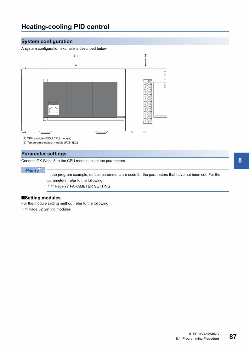
8
Heating-cooling PID control
System configurationA system configuration example is described below.
Parameter settingsConnect GX Works3 to the CPU module to set the parameters.
In the program example, default parameters are used for the parameters that have not been set. For the
parameters, refer to the following.
Page 77 PARAMETER SETTING
■Setting modulesFor the module setting method, refer to the following.
Page 82 Setting modules
(1) CPU module (FX5U CPU module)
(2) Temperature control module (FX5-4LC)
(1) (2)
8 PROGRAMMING8.1 Programming Procedure 87
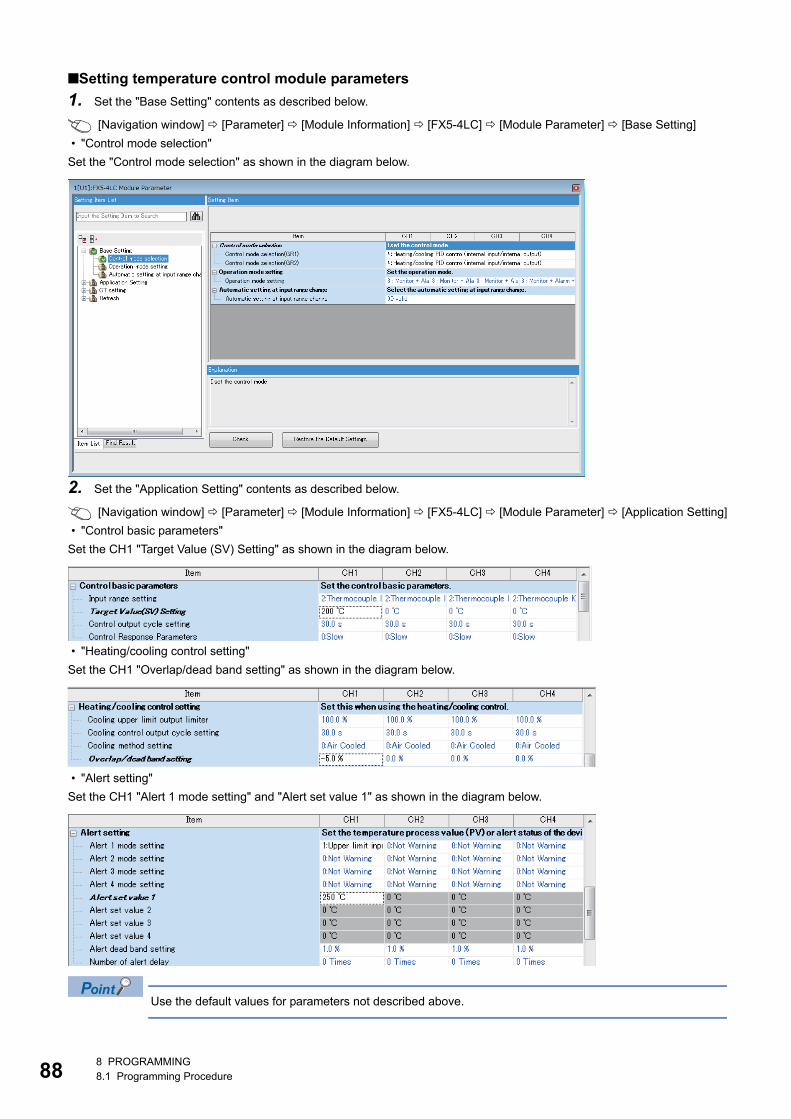
88
■Setting temperature control module parameters
1. Set the "Base Setting" contents as described below.
[Navigation window] [Parameter] [Module Information] [FX5-4LC] [Module Parameter] [Base Setting]
• "Control mode selection"
Set the "Control mode selection" as shown in the diagram below.
2. Set the "Application Setting" contents as described below.
[Navigation window] [Parameter] [Module Information] [FX5-4LC] [Module Parameter] [Application Setting]
• "Control basic parameters"
Set the CH1 "Target Value (SV) Setting" as shown in the diagram below.
• "Heating/cooling control setting"
Set the CH1 "Overlap/dead band setting" as shown in the diagram below.
• "Alert setting"
Set the CH1 "Alert 1 mode setting" and "Alert set value 1" as shown in the diagram below.
Use the default values for parameters not described above.
8 PROGRAMMING8.1 Programming Procedure
8
■Writing to the CPU moduleFor writing to the CPU module, refer to the following.
Auto tuningFor the auto tuning procedure, refer to the following.
Page 85 Auto tuning
Program ExampleFor the program example, refer to the following.
Page 86 Program Example
8 PROGRAMMING8.1 Programming Procedure 89
90
9 TROUBLESHOOTING
This chapter describes errors that may occur when the temperature control module is used and troubleshooting.
9.1 Checks with LEDsBy checking the display status of LEDs, the problem can be primarily diagnosed without GX Works3 and the cause is
narrowed down.
A state of the temperature control module can be checked with the POWER LED, RUN LED, and ERROR LED. The following
table shows the correspondence between each LED status and each state of the temperature control module.
The POWER LED has turned OFFWhen the POWER LED turns OFF, check the following items.
The RUN LED has turned OFFWhen the RUN LED turns OFF, check the following items.
When the ERROR LED turns on or flashesWhen the ERROR LED turns OFF, check the following items.
Name Description
POWER LED Shows the power supply status.
ON: Power supply is ON
OFF: Power supply is OFF or a module error has occurred
RUN LED Shows the operations status.
ON: Normal operation
OFF: Error has occurred
ERROR LED Shows the error status.
ON: Mild or critical error has occurred
Flashing: Moderate or critical error has occurred
OFF: Normal operation
Check item Corrective action
Is the power supplied? Check that the supplied voltage is within the rated range.
Is the capacity insufficient? Calculate the current consumption, and check that the power capacity is not insufficient.
Check item Corrective action
Is the power supplied external 24 V DC? (During
startup only)
Check that the external voltage supply is within the rated range.
Is the temperature control module mounted
correctly? (During startup only)
Check the mounting status of the temperature control module.
Other than above Reset the CPU module, and check that the RUN LED is ON.
If the RUN LED is not ON, it is possible that the module is malfunctioning. Consult your local Mitsubishi
representative, dealer, or branch office to explain the failure symptoms.
Check item Corrective action
Has an error occurred? Check 'Latest error code' (Un\G0), and take a corrective action described in List of Error Codes.
Page 92 List of Error Codes
9 TROUBLESHOOTING9.1 Checks with LEDs
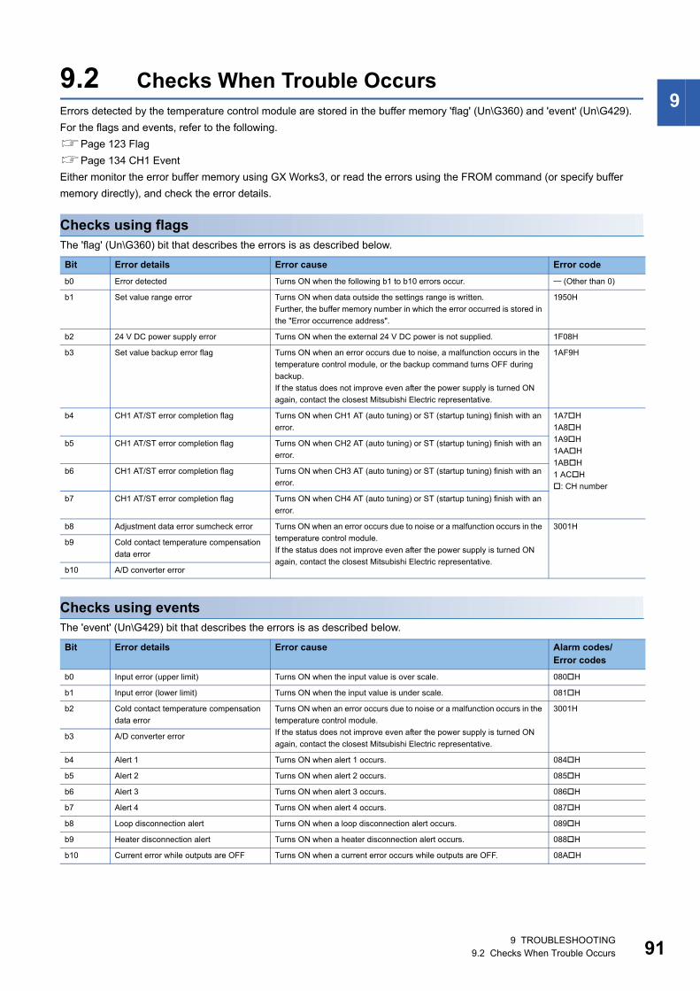
9
9.2 Checks When Trouble OccursErrors detected by the temperature control module are stored in the buffer memory 'flag' (Un\G360) and 'event' (Un\G429).For the flags and events, refer to the following.
Page 123 Flag
Page 134 CH1 Event
Either monitor the error buffer memory using GX Works3, or read the errors using the FROM command (or specify buffer
memory directly), and check the error details.
Checks using flagsThe 'flag' (Un\G360) bit that describes the errors is as described below.
Checks using eventsThe 'event' (Un\G429) bit that describes the errors is as described below.
Bit Error details Error cause Error code
b0 Error detected Turns ON when the following b1 to b10 errors occur. (Other than 0)
b1 Set value range error Turns ON when data outside the settings range is written.
Further, the buffer memory number in which the error occurred is stored in
the "Error occurrence address".
1950H
b2 24 V DC power supply error Turns ON when the external 24 V DC power is not supplied. 1F08H
b3 Set value backup error flag Turns ON when an error occurs due to noise, a malfunction occurs in the
temperature control module, or the backup command turns OFF during
backup.
If the status does not improve even after the power supply is turned ON
again, contact the closest Mitsubishi Electric representative.
1AF9H
b4 CH1 AT/ST error completion flag Turns ON when CH1 AT (auto tuning) or ST (startup tuning) finish with an
error.
1A7H
1A8H
1A9H
1AAH
1ABH
1 ACH
: CH number
b5 CH1 AT/ST error completion flag Turns ON when CH2 AT (auto tuning) or ST (startup tuning) finish with an
error.
b6 CH1 AT/ST error completion flag Turns ON when CH3 AT (auto tuning) or ST (startup tuning) finish with an
error.
b7 CH1 AT/ST error completion flag Turns ON when CH4 AT (auto tuning) or ST (startup tuning) finish with an
error.
b8 Adjustment data error sumcheck error Turns ON when an error occurs due to noise or a malfunction occurs in the
temperature control module.
If the status does not improve even after the power supply is turned ON
again, contact the closest Mitsubishi Electric representative.
3001H
b9 Cold contact temperature compensation
data error
b10 A/D converter error
Bit Error details Error cause Alarm codes/Error codes
b0 Input error (upper limit) Turns ON when the input value is over scale. 080H
b1 Input error (lower limit) Turns ON when the input value is under scale. 081H
b2 Cold contact temperature compensation
data error
Turns ON when an error occurs due to noise or a malfunction occurs in the
temperature control module.
If the status does not improve even after the power supply is turned ON
again, contact the closest Mitsubishi Electric representative.
3001H
b3 A/D converter error
b4 Alert 1 Turns ON when alert 1 occurs. 084H
b5 Alert 2 Turns ON when alert 2 occurs. 085H
b6 Alert 3 Turns ON when alert 3 occurs. 086H
b7 Alert 4 Turns ON when alert 4 occurs. 087H
b8 Loop disconnection alert Turns ON when a loop disconnection alert occurs. 089H
b9 Heater disconnection alert Turns ON when a heater disconnection alert occurs. 088H
b10 Current error while outputs are OFF Turns ON when a current error occurs while outputs are OFF. 08AH
9 TROUBLESHOOTING9.2 Checks When Trouble Occurs 91
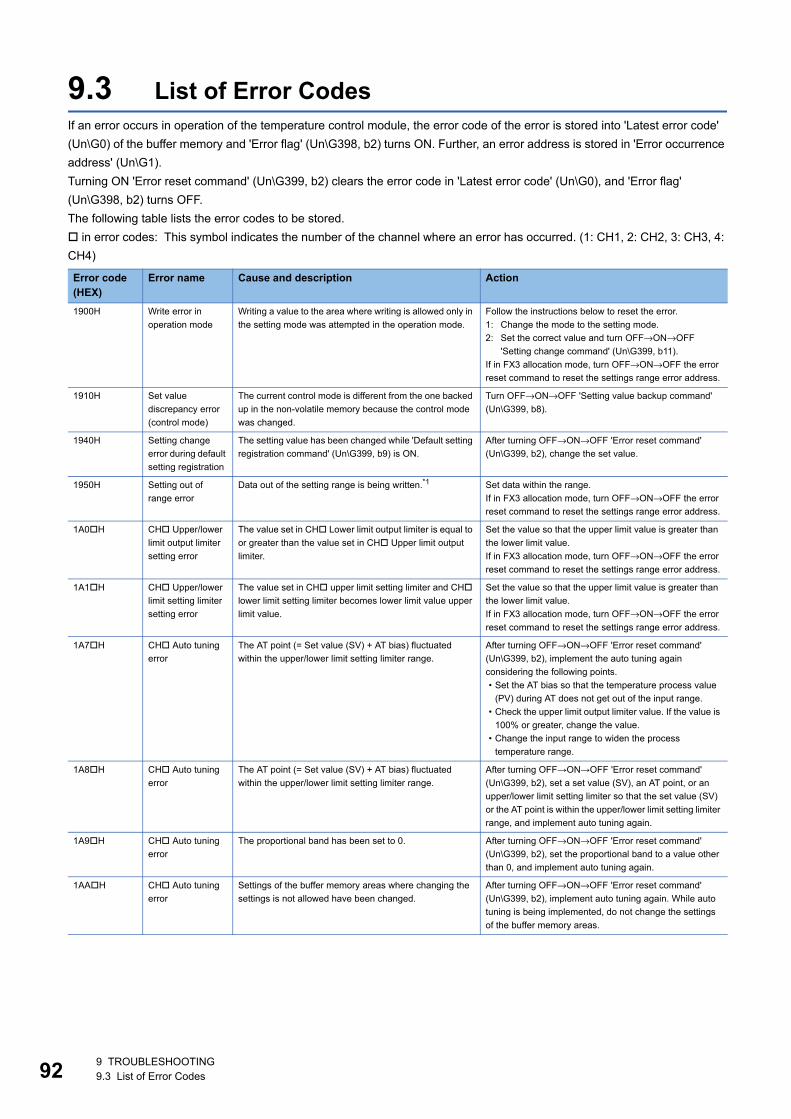
92
9.3 List of Error CodesIf an error occurs in operation of the temperature control module, the error code of the error is stored into 'Latest error code'
(Un\G0) of the buffer memory and 'Error flag' (Un\G398, b2) turns ON. Further, an error address is stored in 'Error occurrence
address' (Un\G1).
Turning ON 'Error reset command' (Un\G399, b2) clears the error code in 'Latest error code' (Un\G0), and 'Error flag'
(Un\G398, b2) turns OFF.
The following table lists the error codes to be stored.
in error codes: This symbol indicates the number of the channel where an error has occurred. (1: CH1, 2: CH2, 3: CH3, 4:
CH4)
Error code(HEX)
Error name Cause and description Action
1900H Write error in
operation mode
Writing a value to the area where writing is allowed only in
the setting mode was attempted in the operation mode.
Follow the instructions below to reset the error.
1: Change the mode to the setting mode.
2: Set the correct value and turn OFF→ON→OFF
'Setting change command' (Un\G399, b11).
If in FX3 allocation mode, turn OFF→ON→OFF the error
reset command to reset the settings range error address.
1910H Set value
discrepancy error
(control mode)
The current control mode is different from the one backed
up in the non-volatile memory because the control mode
was changed.
Turn OFF→ON→OFF 'Setting value backup command'
(Un\G399, b8).
1940H Setting change
error during default
setting registration
The setting value has been changed while 'Default setting
registration command' (Un\G399, b9) is ON.
After turning OFF→ON→OFF 'Error reset command'
(Un\G399, b2), change the set value.
1950H Setting out of
range error
Data out of the setting range is being written.*1 Set data within the range.
If in FX3 allocation mode, turn OFF→ON→OFF the error
reset command to reset the settings range error address.
1A0H CH Upper/lower
limit output limiter
setting error
The value set in CH Lower limit output limiter is equal to
or greater than the value set in CH Upper limit output
limiter.
Set the value so that the upper limit value is greater than
the lower limit value.
If in FX3 allocation mode, turn OFF→ON→OFF the error
reset command to reset the settings range error address.
1A1H CH Upper/lower
limit setting limiter
setting error
The value set in CH upper limit setting limiter and CH
lower limit setting limiter becomes lower limit value upper
limit value.
Set the value so that the upper limit value is greater than
the lower limit value.
If in FX3 allocation mode, turn OFF→ON→OFF the error
reset command to reset the settings range error address.
1A7H CH Auto tuning
error
The AT point (= Set value (SV) + AT bias) fluctuated
within the upper/lower limit setting limiter range.
After turning OFF→ON→OFF 'Error reset command'
(Un\G399, b2), implement the auto tuning again
considering the following points.
• Set the AT bias so that the temperature process value
(PV) during AT does not get out of the input range.
• Check the upper limit output limiter value. If the value is
100% or greater, change the value.
• Change the input range to widen the process
temperature range.
1A8H CH Auto tuning
error
The AT point (= Set value (SV) + AT bias) fluctuated
within the upper/lower limit setting limiter range.
After turning OFF→ON→OFF 'Error reset command'
(Un\G399, b2), set a set value (SV), an AT point, or an
upper/lower limit setting limiter so that the set value (SV)
or the AT point is within the upper/lower limit setting limiter
range, and implement auto tuning again.
1A9H CH Auto tuning
error
The proportional band has been set to 0. After turning OFF→ON→OFF 'Error reset command'
(Un\G399, b2), set the proportional band to a value other
than 0, and implement auto tuning again.
1AAH CH Auto tuning
error
Settings of the buffer memory areas where changing the
settings is not allowed have been changed.
After turning OFF→ON→OFF 'Error reset command'
(Un\G399, b2), implement auto tuning again. While auto
tuning is being implemented, do not change the settings
of the buffer memory areas.
9 TROUBLESHOOTING9.3 List of Error Codes
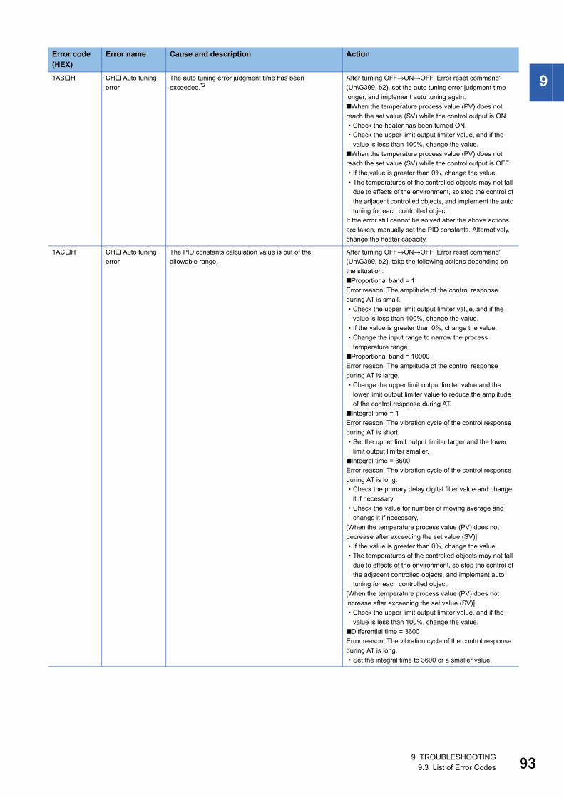
9
1ABH CH Auto tuningerror
The auto tuning error judgment time has been
exceeded.*2After turning OFF→ON→OFF 'Error reset command'
(Un\G399, b2), set the auto tuning error judgment time
longer, and implement auto tuning again.
■When the temperature process value (PV) does not
reach the set value (SV) while the control output is ON
• Check the heater has been turned ON.
• Check the upper limit output limiter value, and if the
value is less than 100%, change the value.
■When the temperature process value (PV) does not
reach the set value (SV) while the control output is OFF
• If the value is greater than 0%, change the value.
• The temperatures of the controlled objects may not fall
due to effects of the environment, so stop the control of
the adjacent controlled objects, and implement the auto
tuning for each controlled object.
If the error still cannot be solved after the above actions
are taken, manually set the PID constants. Alternatively,
change the heater capacity.
1ACH CH Auto tuning
error
The PID constants calculation value is out of the
allowable range.
After turning OFF→ON→OFF 'Error reset command'
(Un\G399, b2), take the following actions depending on
the situation.
■Proportional band = 1
Error reason: The amplitude of the control response
during AT is small.
• Check the upper limit output limiter value, and if the
value is less than 100%, change the value.
• If the value is greater than 0%, change the value.
• Change the input range to narrow the process
temperature range.
■Proportional band = 10000
Error reason: The amplitude of the control response
during AT is large.
• Change the upper limit output limiter value and the
lower limit output limiter value to reduce the amplitude
of the control response during AT.
■Integral time = 1
Error reason: The vibration cycle of the control response
during AT is short.
• Set the upper limit output limiter larger and the lower
limit output limiter smaller.
■Integral time = 3600
Error reason: The vibration cycle of the control response
during AT is long.
• Check the primary delay digital filter value and change
it if necessary.
• Check the value for number of moving average and
change it if necessary.
[When the temperature process value (PV) does not
decrease after exceeding the set value (SV)]
• If the value is greater than 0%, change the value.
• The temperatures of the controlled objects may not fall
due to effects of the environment, so stop the control of
the adjacent controlled objects, and implement auto
tuning for each controlled object.
[When the temperature process value (PV) does not
increase after exceeding the set value (SV)]
• Check the upper limit output limiter value, and if the
value is less than 100%, change the value.
■Differential time = 3600
Error reason: The vibration cycle of the control response
during AT is long.
• Set the integral time to 3600 or a smaller value.
Error code(HEX)
Error name Cause and description Action
9 TROUBLESHOOTING9.3 List of Error Codes 93
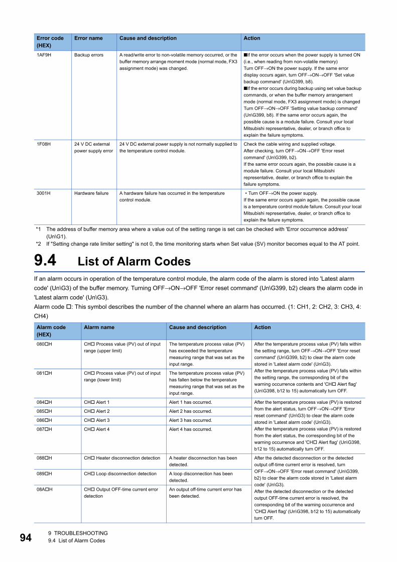
94
*1 The address of buffer memory area where a value out of the setting range is set can be checked with 'Error occurrence address' (Un\G1).
*2 If "Setting change rate limiter setting" is not 0, the time monitoring starts when Set value (SV) monitor becomes equal to the AT point.
9.4 List of Alarm CodesIf an alarm occurs in operation of the temperature control module, the alarm code of the alarm is stored into 'Latest alarm
code' (Un\G3) of the buffer memory. Turning OFF→ON→OFF 'Error reset command' (Un\G399, b2) clears the alarm code in
'Latest alarm code' (Un\G3).
Alarm code : This symbol describes the number of the channel where an alarm has occurred. (1: CH1, 2: CH2, 3: CH3, 4:
CH4)
1AF9H Backup errors A read/write error to non-volatile memory occurred, or the
buffer memory arrange moment mode (normal mode, FX3
assignment mode) was changed.
■If the error occurs when the power supply is turned ON
(i.e., when reading from non-volatile memory)
Turn OFF→ON the power supply. If the same error
display occurs again, turn OFF→ON→OFF 'Set value
backup command' (Un\G399, b8).
■If the error occurs during backup using set value backup
commands, or when the buffer memory arrangement
mode (normal mode, FX3 assignment mode) is changed
Turn OFF→ON→OFF 'Setting value backup command'
(Un\G399, b8). If the same error occurs again, the
possible cause is a module failure. Consult your local
Mitsubishi representative, dealer, or branch office to
explain the failure symptoms.
1F08H 24 V DC external
power supply error
24 V DC external power supply is not normally supplied to
the temperature control module.
Check the cable wiring and supplied voltage.
After checking, turn OFF→ON→OFF 'Error reset
command' (Un\G399, b2).
If the same error occurs again, the possible cause is a
module failure. Consult your local Mitsubishi
representative, dealer, or branch office to explain the
failure symptoms.
3001H Hardware failure A hardware failure has occurred in the temperature
control module.
• Turn OFF→ON the power supply.
If the same error occurs again again, the possible cause
is a temperature control module failure. Consult your local
Mitsubishi representative, dealer, or branch office to
explain the failure symptoms.
Alarm code(HEX)
Alarm name Cause and description Action
080H CH Process value (PV) out of input
range (upper limit)
The temperature process value (PV)
has exceeded the temperature
measuring range that was set as the
input range.
After the temperature process value (PV) falls within
the setting range, turn OFF→ON→OFF 'Error reset
command' (Un\G399, b2) to clear the alarm code
stored in 'Latest alarm code' (Un\G3).
After the temperature process value (PV) falls within
the setting range, the corresponding bit of the
warning occurrence contents and 'CH Alert flag'
(Un\G398, b12 to 15) automatically turn OFF.
081H CH Process value (PV) out of input
range (lower limit)
The temperature process value (PV)
has fallen below the temperature
measuring range that was set as the
input range.
084H CH Alert 1 Alert 1 has occurred. After the temperature process value (PV) is restored
from the alert status, turn OFF→ON→OFF 'Error
reset command' (Un\G3) to clear the alarm code
stored in 'Latest alarm code' (Un\G3).
After the temperature process value (PV) is restored
from the alert status, the corresponding bit of the
warning occurrence and 'CH Alert flag' (Un\G398,
b12 to 15) automatically turn OFF.
085H CH Alert 2 Alert 2 has occurred.
086H CH Alert 3 Alert 3 has occurred.
087H CH Alert 4 Alert 4 has occurred.
088H CH Heater disconnection detection A heater disconnection has been
detected.
After the detected disconnection or the detected
output off-time current error is resolved, turn
OFF→ON→OFF 'Error reset command' (Un\G399,
b2) to clear the alarm code stored in 'Latest alarm
code' (Un\G3).
After the detected disconnection or the detected
output OFF-time current error is resolved, the
corresponding bit of the warning occurrence and
'CH Alert flag' (Un\G398, b12 to 15) automatically
turn OFF.
089H CH Loop disconnection detection A loop disconnection has been
detected.
08AH CH Output OFF-time current error
detection
An output off-time current error has
been detected.
Error code(HEX)
Error name Cause and description Action
9 TROUBLESHOOTING9.4 List of Alarm Codes
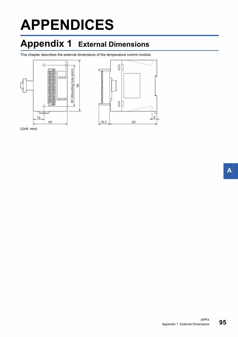
A
APPENDICESAppendix 1 External DimensionsThis chapter describes the external dimensions of the temperature control module.
(Unit: mm)
6019
90
80 (M
ount
ing
hole
pitc
h)
88319.2
APPXAppendix 1 External Dimensions 95
96
Appendix 2 Standards
Certification of UL, cUL standardsThe FX5-4LC supports UL (UL, cUL) standards.
For models that support UL standards, refer to the following.
UL, cUL file number: E95239
Compliance with EC directive (CE Marking)This note does not guarantee that an entire machine produced in accordance with the contents of this note will comply with
the following standards.
Compliance to EMC directive and LVD directive of the entire mechanical module should be checked by the user/
manufacturer. For more details please contact to the local Mitsubishi Electric sales site.
Requirement for compliance with EMC directiveThe following products have shown compliance through direct testing (of the identified standards below) and design analysis
(through the creation of a technical construction file) to the European Directive for Electromagnetic Compatibility (2014/30/
EU) when used as directed by the appropriate documentation.
AttentionThis product is designed for use in industrial applications.
Product compatibilityType: Programmable controller (open type equipment)
Models: FX5 manufactured
from April 1st, 2017 FX5-4LC
Electromagnetic compatibility (EMC) directive Remarks
EN61131-2:2007 Programmable controllers
- Equipment requirements and tests
Compliance with all relevant aspects of the standard.
EMI
• Radiated emission
• Conducted emission
EMS
• Radiated electromagnetic field
• Fast transient burst
• Electrostatic discharge
• High-energy surge
• Voltage drops and interruptions
• Conducted RF
• Power frequency magnetic field
APPXAppendix 2 Standards
A
If accuracy in measuring and control is required when using in an environment exposed to electrical stress,
such as an EMS test, implementing the following details is recommended.
For users of proprietary cables (dedicated for sensors or actuators), these users should follow those
manufacturers' installation requirements.
Mitsubishi Electric recommends that shielded cables be used. If no other EMC protection is provided, users
may experience temporary loss of accuracy between +10%/-10% in very heavy industrial areas.
However, Mitsubishi Electric suggests that if adequate EMC precautions are followed with general good EMC
practice for the user's complete control system, users should expect normal errors as specified in this manual.
• Sensitive analog cables should not be laid in the same trunking or cable conduit as high voltage cabling.
Where possible, users should run analog cables separately.
• Good cable shielding should be used. When terminating the shield at Earth - ensure that no earth loops are
accidentally created.
• When reading analog values, EMC induced errors can be smoothed out by averaging the readings. This
can be achieved either through functions on the analog devices or through a user's program.
APPXAppendix 2 Standards 97
98
Appendix 3 Module LabelThe buffer memory of the temperature control module can be set by using module labels.
Not compatible with FX3 allocation mode.
Module label configurationThe names of the module labels are defined using the following configuration.
"Module name"_"Module number"."Data type"_Ch ["(Channel)"]."Data format""Label name"_D
Ex.
FX5LC_1.stnMonitor_Ch[0].wTemperatureProcessValue_D
■Module nameThe module name indicates the model of the module.
■Module numberThe module number starts from one and increments for identifying modules with the same module name.
■Data typeThe data type indicates the type of a buffer memory area. The following shows the classification.
■ChannelThis part indicates the channel number corresponding to a module label. A numerical value of 0 to 3 is stored to correspond to
CH1 to CH4.
(CH1: 0, CH2: 1, CH3: 2, CH4: 3)
■Data typeThe data type indicates the size of a buffer memory area. The following shows the classification.
■Label NameThe label name is unique by modules.
■_D_D indicates that the module label is for direct access.
Data type Description
stnMonitor Monitor
stnControl Control
stnSetting Setting
Data type Description
b Bit
u Word [Unsigned]/Bit String [16-bit]
w Word [Signed]
st Structure
z System area
n Array format (: b, u, w, st)
Type Description Access timing
Direct access Values that has been read from or written to module labels are immediately
applied to the module. The run time of a program is longer than the one for auto
refresh. However, the responsiveness is high.
At reading/writing data from/to the module label
APPXAppendix 3 Module Label
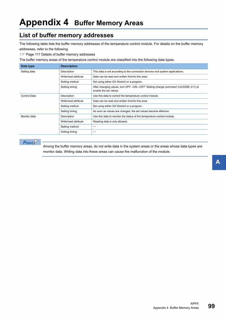
A
Appendix 4 Buffer Memory Areas
List of buffer memory addressesThe following table lists the buffer memory addresses of the temperature control module. For details on the buffer memory
addresses, refer to the following.
Page 117 Details of buffer memory addresses
The buffer memory areas of the temperature control module are classified into the following data types.
Among the buffer memory areas, do not write data in the system areas or the areas whose data types are
monitor data. Writing data into these areas can cause the malfunction of the module.
Data type Description
Setting data Description This data is set according to the connection devices and system applications.
Write/read attribute Data can be read and written from/to this area.
Setting method Set using either GX Works3 or a program.
Setting timing After changing values, turn OFF→ON→OFF 'Setting change command' (Un\G399, b11) to
enable the set values.
Control Data Description Use this data to control the temperature control module.
Write/read attribute Data can be read and written from/to this area.
Setting method Set using either GX Works3 or a program.
Setting timing As soon as values are changed, the set values become effective.
Monitor data Description Use this data to monitor the status of the temperature control module.
Write/read attribute Reading data is only allowed.
Setting method
Setting timing
APPXAppendix 4 Buffer Memory Areas 99
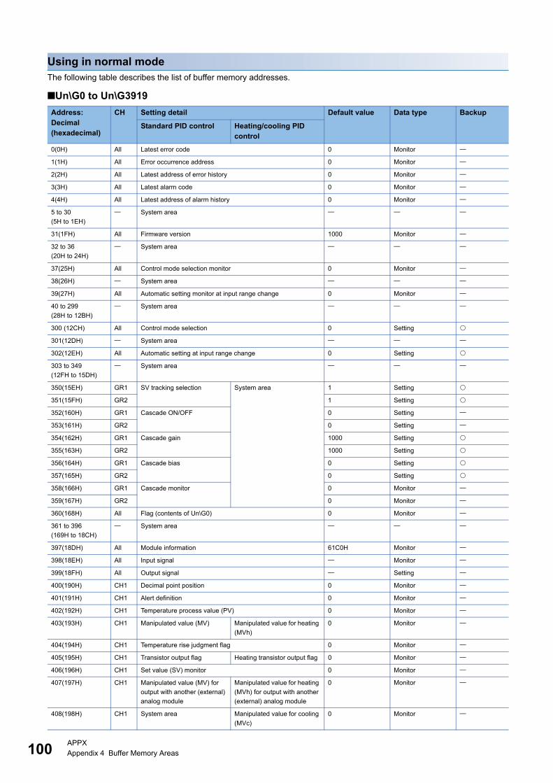
10
Using in normal modeThe following table describes the list of buffer memory addresses.
■Un\G0 to Un\G3919
Address: Decimal (hexadecimal)
CH Setting detail Default value Data type Backup
Standard PID control Heating/cooling PID control
0(0H) All Latest error code 0 Monitor
1(1H) All Error occurrence address 0 Monitor
2(2H) All Latest address of error history 0 Monitor
3(3H) All Latest alarm code 0 Monitor
4(4H) All Latest address of alarm history 0 Monitor
5 to 30
(5H to 1EH)
System area
31(1FH) All Firmware version 1000 Monitor
32 to 36
(20H to 24H)
System area
37(25H) All Control mode selection monitor 0 Monitor
38(26H) System area
39(27H) All Automatic setting monitor at input range change 0 Monitor
40 to 299
(28H to 12BH)
System area
300 (12CH) All Control mode selection 0 Setting
301(12DH) System area
302(12EH) All Automatic setting at input range change 0 Setting
303 to 349
(12FH to 15DH)
System area
350(15EH) GR1 SV tracking selection System area 1 Setting
351(15FH) GR2 1 Setting
352(160H) GR1 Cascade ON/OFF 0 Setting
353(161H) GR2 0 Setting
354(162H) GR1 Cascade gain 1000 Setting
355(163H) GR2 1000 Setting
356(164H) GR1 Cascade bias 0 Setting
357(165H) GR2 0 Setting
358(166H) GR1 Cascade monitor 0 Monitor
359(167H) GR2 0 Monitor
360(168H) All Flag (contents of Un\G0) 0 Monitor
361 to 396
(169H to 18CH)
System area
397(18DH) All Module information 61C0H Monitor
398(18EH) All Input signal Monitor
399(18FH) All Output signal Setting
400(190H) CH1 Decimal point position 0 Monitor
401(191H) CH1 Alert definition 0 Monitor
402(192H) CH1 Temperature process value (PV) 0 Monitor
403(193H) CH1 Manipulated value (MV) Manipulated value for heating
(MVh)
0 Monitor
404(194H) CH1 Temperature rise judgment flag 0 Monitor
405(195H) CH1 Transistor output flag Heating transistor output flag 0 Monitor
406(196H) CH1 Set value (SV) monitor 0 Monitor
407(197H) CH1 Manipulated value (MV) for
output with another (external)
analog module
Manipulated value for heating
(MVh) for output with another
(external) analog module
0 Monitor
408(198H) CH1 System area Manipulated value for cooling
(MVc)
0 Monitor
0APPXAppendix 4 Buffer Memory Areas
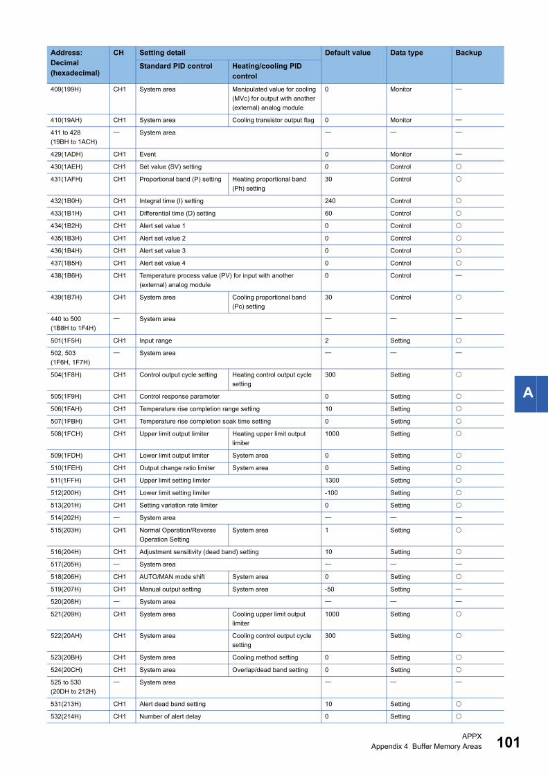
A
409(199H) CH1 System area Manipulated value for cooling
(MVc) for output with another
(external) analog module
0 Monitor
410(19AH) CH1 System area Cooling transistor output flag 0 Monitor
411 to 428
(19BH to 1ACH)
System area
429(1ADH) CH1 Event 0 Monitor
430(1AEH) CH1 Set value (SV) setting 0 Control
431(1AFH) CH1 Proportional band (P) setting Heating proportional band
(Ph) setting
30 Control
432(1B0H) CH1 Integral time (I) setting 240 Control
433(1B1H) CH1 Differential time (D) setting 60 Control
434(1B2H) CH1 Alert set value 1 0 Control
435(1B3H) CH1 Alert set value 2 0 Control
436(1B4H) CH1 Alert set value 3 0 Control
437(1B5H) CH1 Alert set value 4 0 Control
438(1B6H) CH1 Temperature process value (PV) for input with another
(external) analog module
0 Control
439(1B7H) CH1 System area Cooling proportional band
(Pc) setting
30 Control
440 to 500
(1B8H to 1F4H)
System area
501(1F5H) CH1 Input range 2 Setting
502, 503
(1F6H, 1F7H)
System area
504(1F8H) CH1 Control output cycle setting Heating control output cycle
setting
300 Setting
505(1F9H) CH1 Control response parameter 0 Setting
506(1FAH) CH1 Temperature rise completion range setting 10 Setting
507(1FBH) CH1 Temperature rise completion soak time setting 0 Setting
508(1FCH) CH1 Upper limit output limiter Heating upper limit output
limiter
1000 Setting
509(1FDH) CH1 Lower limit output limiter System area 0 Setting
510(1FEH) CH1 Output change ratio limiter System area 0 Setting
511(1FFH) CH1 Upper limit setting limiter 1300 Setting
512(200H) CH1 Lower limit setting limiter -100 Setting
513(201H) CH1 Setting variation rate limiter 0 Setting
514(202H) System area
515(203H) CH1 Normal Operation/Reverse
Operation Setting
System area 1 Setting
516(204H) CH1 Adjustment sensitivity (dead band) setting 10 Setting
517(205H) System area
518(206H) CH1 AUTO/MAN mode shift System area 0 Setting
519(207H) CH1 Manual output setting System area -50 Setting
520(208H) System area
521(209H) CH1 System area Cooling upper limit output
limiter
1000 Setting
522(20AH) CH1 System area Cooling control output cycle
setting
300 Setting
523(20BH) CH1 System area Cooling method setting 0 Setting
524(20CH) CH1 System area Overlap/dead band setting 0 Setting
525 to 530
(20DH to 212H)
System area
531(213H) CH1 Alert dead band setting 10 Setting
532(214H) CH1 Number of alert delay 0 Setting
Address: Decimal (hexadecimal)
CH Setting detail Default value Data type Backup
Standard PID control Heating/cooling PID control
APPXAppendix 4 Buffer Memory Areas 101
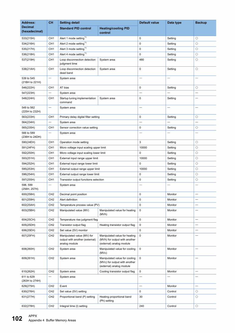
10
533(215H) CH1 Alert 1 mode setting*1 0 Setting
534(216H) CH1 Alert 2 mode setting*1 0 Setting
535(217H) CH1 Alert 3 mode setting*1 0 Setting
536(218H) CH1 Alert 4 mode setting*1 0 Setting
537(219H) CH1 Loop disconnection detection
judgment time
System area 480 Setting
538(21AH) CH1 Loop disconnection detection
dead band
System area 0 Setting
539 to 545
(21BH to 221H)
System area
546(222H) CH1 AT bias 0 Setting
547(223H) System area
548(224H) CH1 Startup tuning implementation
command
System area 0 Setting
549 to 562
(225H to 232H)
System area
563(233H) CH1 Primary delay digital filter setting 0 Setting
564(234H) System area
565(235H) CH1 Sensor correction value setting 0 Setting
566 to 589
(236H to 24DH)
System area
590(24EH) CH1 Operation mode setting 3 Setting
591(24FH) CH1 Micro voltage input scaling upper limit 10000 Setting
592(250H) CH1 Micro voltage input scaling lower limit 0 Setting
593(251H) CH1 External input range upper limit 10000 Setting
594(252H) CH1 External input range lower limit 0 Setting
595(253H) CH1 External output range upper limit 10000 Setting
596(254H) CH1 External output range lower limit 0 Setting
597(255H) CH1 Transistor output functions selection 0 Setting
598, 599
(256H, 257H)
System area
600(258H) CH2 Decimal point position 0 Monitor
601(259H) CH2 Alert definition 0 Monitor
602(25AH) CH2 Temperature process value (PV) 0 Monitor
603(25BH) CH2 Manipulated value (MV) Manipulated value for heating
(MVh)
0 Monitor
604(25CH) CH2 Temperature rise judgment flag 0 Monitor
605(25DH) CH2 Transistor output flag Heating transistor output flag 0 Monitor
606(25EH) CH2 Set value (SV) monitor 0 Monitor
607(25FH) CH2 Manipulated value (MV) for
output with another (external)
analog module
Manipulated value for heating
(MVh) for output with another
(external) analog module
0 Monitor
608(260H) CH2 System area Manipulated value for cooling
(MVc)
0 Monitor
609(261H) CH2 System area Manipulated value for cooling
(MVc) for output with another
(external) analog module
0 Monitor
610(262H) CH2 System area Cooling transistor output flag 0 Monitor
611 to 629
(263H to 274H)
System area
629(275H) CH2 Event Monitor
630(276H) CH2 Set value (SV) setting 0 Control
631(277H) CH2 Proportional band (P) setting Heating proportional band
(Ph) setting
30 Control
632(278H) CH2 Integral time (I) setting 240 Control
Address: Decimal (hexadecimal)
CH Setting detail Default value Data type Backup
Standard PID control Heating/cooling PID control
2APPXAppendix 4 Buffer Memory Areas
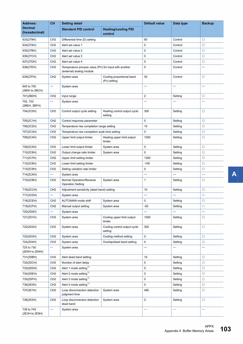
A
633(279H) CH2 Differential time (D) setting 60 Control
634(27AH) CH2 Alert set value 1 0 Control
635(27BH) CH2 Alert set value 2 0 Control
636(27CH) CH2 Alert set value 3 0 Control
637(27DH) CH2 Alert set value 4 0 Control
638(27EH) CH2 Temperature process value (PV) for input with another
(external) analog module
0 Control
639(27FH) CH2 System area Cooling proportional band
(Pc) setting
30 Control
640 to 700
(280H to 2BCH)
System area
701(2BDH) CH2 Input range 2 Setting
702, 703
(2BEH, 2BFH)
System area
704(2C0H) CH2 Control output cycle setting Heating control output cycle
setting
300 Setting
705(2C1H) CH2 Control response parameter 0 Setting
706(2C2H) CH2 Temperature rise completion range setting 10 Setting
707(2C3H) CH2 Temperature rise completion soak time setting 0 Setting
708(2C4H) CH2 Upper limit output limiter Heating upper limit output
limiter
1000 Setting
709(2C5H) CH2 Lower limit output limiter System area 0 Setting
710(2C6H) CH2 Output change ratio limiter System area 0 Setting
711(2C7H) CH2 Upper limit setting limiter 1300 Setting
712(2C8H) CH2 Lower limit setting limiter -100 Setting
713(2C9H) CH2 Setting variation rate limiter 0 Setting
714(2CAH) System area
715(2CBH) CH2 Normal Operation/Reverse
Operation Setting
System area 1 Setting
716(2CCH) CH2 Adjustment sensitivity (dead band) setting 10 Setting
717(2CDH) System area
718(2CEH) CH2 AUTO/MAN mode shift System area 0 Setting
719(2CFH) CH2 Manual output setting System area -50 Setting
720(2D0H) System area
721(2D1H) CH2 System area Cooling upper limit output
limiter
1000 Setting
722(2D2H) CH2 System area Cooling control output cycle
setting
300 Setting
723(2D3H) CH2 System area Cooling method setting 0 Setting
724(2D4H) CH2 System area Overlap/dead band setting 0 Setting
725 to 730
(2D5H to 2DAH)
System area
731(2DBH) CH2 Alert dead band setting 10 Setting
732(2DCH) CH2 Number of alert delay 0 Setting
733(2DDH) CH2 Alert 1 mode setting*1 0 Setting
734(2DEH) CH2 Alert 2 mode setting*1 0 Setting
735(2DFH) CH2 Alert 3 mode setting*1 0 Setting
736(2E0H) CH2 Alert 4 mode setting*1 0 Setting
737(2E1H) CH2 Loop disconnection detection
judgment time
System area 480 Setting
738(2E2H) CH2 Loop disconnection detection
dead band
System area 0 Setting
739 to 745
(2E3H to 2E9H)
System area
Address: Decimal (hexadecimal)
CH Setting detail Default value Data type Backup
Standard PID control Heating/cooling PID control
APPXAppendix 4 Buffer Memory Areas 103
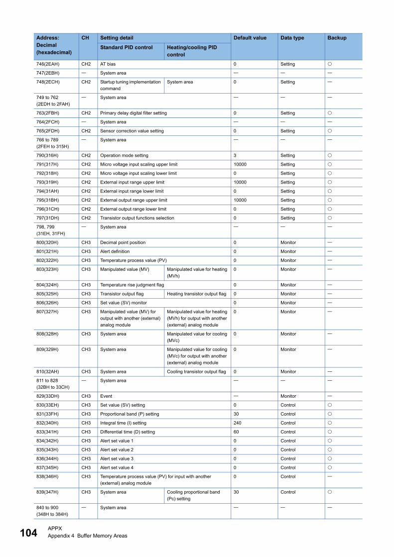
10
746(2EAH) CH2 AT bias 0 Setting
747(2EBH) System area
748(2ECH) CH2 Startup tuning implementation
command
System area 0 Setting
749 to 762
(2EDH to 2FAH)
System area
763(2FBH) CH2 Primary delay digital filter setting 0 Setting
764(2FCH) System area
765(2FDH) CH2 Sensor correction value setting 0 Setting
766 to 789
(2FEH to 315H)
System area
790(316H) CH2 Operation mode setting 3 Setting
791(317H) CH2 Micro voltage input scaling upper limit 10000 Setting
792(318H) CH2 Micro voltage input scaling lower limit 0 Setting
793(319H) CH2 External input range upper limit 10000 Setting
794(31AH) CH2 External input range lower limit 0 Setting
795(31BH) CH2 External output range upper limit 10000 Setting
796(31CH) CH2 External output range lower limit 0 Setting
797(31DH) CH2 Transistor output functions selection 0 Setting
798, 799
(31EH, 31FH)
System area
800(320H) CH3 Decimal point position 0 Monitor
801(321H) CH3 Alert definition 0 Monitor
802(322H) CH3 Temperature process value (PV) 0 Monitor
803(323H) CH3 Manipulated value (MV) Manipulated value for heating
(MVh)
0 Monitor
804(324H) CH3 Temperature rise judgment flag 0 Monitor
805(325H) CH3 Transistor output flag Heating transistor output flag 0 Monitor
806(326H) CH3 Set value (SV) monitor 0 Monitor
807(327H) CH3 Manipulated value (MV) for
output with another (external)
analog module
Manipulated value for heating
(MVh) for output with another
(external) analog module
0 Monitor
808(328H) CH3 System area Manipulated value for cooling
(MVc)
0 Monitor
809(329H) CH3 System area Manipulated value for cooling
(MVc) for output with another
(external) analog module
0 Monitor
810(32AH) CH3 System area Cooling transistor output flag 0 Monitor
811 to 828
(32BH to 33CH)
System area
829(33DH) CH3 Event Monitor
830(33EH) CH3 Set value (SV) setting 0 Control
831(33FH) CH3 Proportional band (P) setting 30 Control
832(340H) CH3 Integral time (I) setting 240 Control
833(341H) CH3 Differential time (D) setting 60 Control
834(342H) CH3 Alert set value 1 0 Control
835(343H) CH3 Alert set value 2 0 Control
836(344H) CH3 Alert set value 3 0 Control
837(345H) CH3 Alert set value 4 0 Control
838(346H) CH3 Temperature process value (PV) for input with another
(external) analog module
0 Control
839(347H) CH3 System area Cooling proportional band
(Pc) setting
30 Control
840 to 900
(348H to 384H)
System area
Address: Decimal (hexadecimal)
CH Setting detail Default value Data type Backup
Standard PID control Heating/cooling PID control
4APPXAppendix 4 Buffer Memory Areas
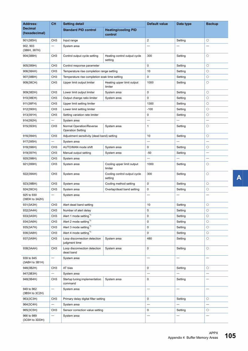
A
901(385H) CH3 Input range 2 Setting
902, 903
(386H, 387H)
System area
904(388H) CH3 Control output cycle setting Heating control output cycle
setting
300 Setting
905(389H) CH3 Control response parameter 0 Setting
906(38AH) CH3 Temperature rise completion range setting 10 Setting
907(38BH) CH3 Temperature rise completion soak time setting 0 Setting
908(38CH) CH3 Upper limit output limiter Heating upper limit output
limiter
1000 Setting
909(38DH) CH3 Lower limit output limiter System area 0 Setting
910(38EH) CH3 Output change ratio limiter System area 0 Setting
911(38FH) CH3 Upper limit setting limiter 1300 Setting
912(390H) CH3 Lower limit setting limiter -100 Setting
913(391H) CH3 Setting variation rate limiter 0 Setting
914(392H) System area
915(393H) CH3 Normal Operation/Reverse
Operation Setting
System area 1 Setting
916(394H) CH3 Adjustment sensitivity (dead band) setting 10 Setting
917(395H) System area
918(396H) CH3 AUTO/MAN mode shift System area 0 Setting
919(397H) CH3 Manual output setting System area -50 Setting
920(398H) CH3 System area
921(399H) CH3 System area Cooling upper limit output
limiter
1000 Setting
922(39AH) CH3 System area Cooling control output cycle
setting
300 Setting
923(39BH) CH3 System area Cooling method setting 0 Setting
924(39CH) CH3 System area Overlap/dead band setting 0 Setting
925 to 930
(39DH to 3A2H)
System area
931(3A3H) CH3 Alert dead band setting 10 Setting
932(3A4H) CH3 Number of alert delay 0 Setting
933(3A5H) CH3 Alert 1 mode setting*1 0 Setting
934(3A6H) CH3 Alert 2 mode setting*1 0 Setting
935(3A7H) CH3 Alert 3 mode setting*1 0 Setting
936(3A8H) CH3 Alert 4 mode setting*1 0 Setting
937(3A9H) CH3 Loop disconnection detection
judgment time
System area 480 Setting
938(3AAH) CH3 Loop disconnection detection
dead band
System area 0 Setting
939 to 945
(3ABH to 3B1H)
System area
946(3B2H) CH3 AT bias 0 Setting
947(3B3H) System area
948(3B4H) CH3 Startup tuning implementation
command
System area 0 Setting
949 to 962
(3B5H to 3C2H)
System area
963(3C3H) CH3 Primary delay digital filter setting 0 Setting
964(3C4H) System area
965(3C5H) CH3 Sensor correction value setting 0 Setting
966 to 989
(3C6H to 3DDH)
System area
Address: Decimal (hexadecimal)
CH Setting detail Default value Data type Backup
Standard PID control Heating/cooling PID control
APPXAppendix 4 Buffer Memory Areas 105
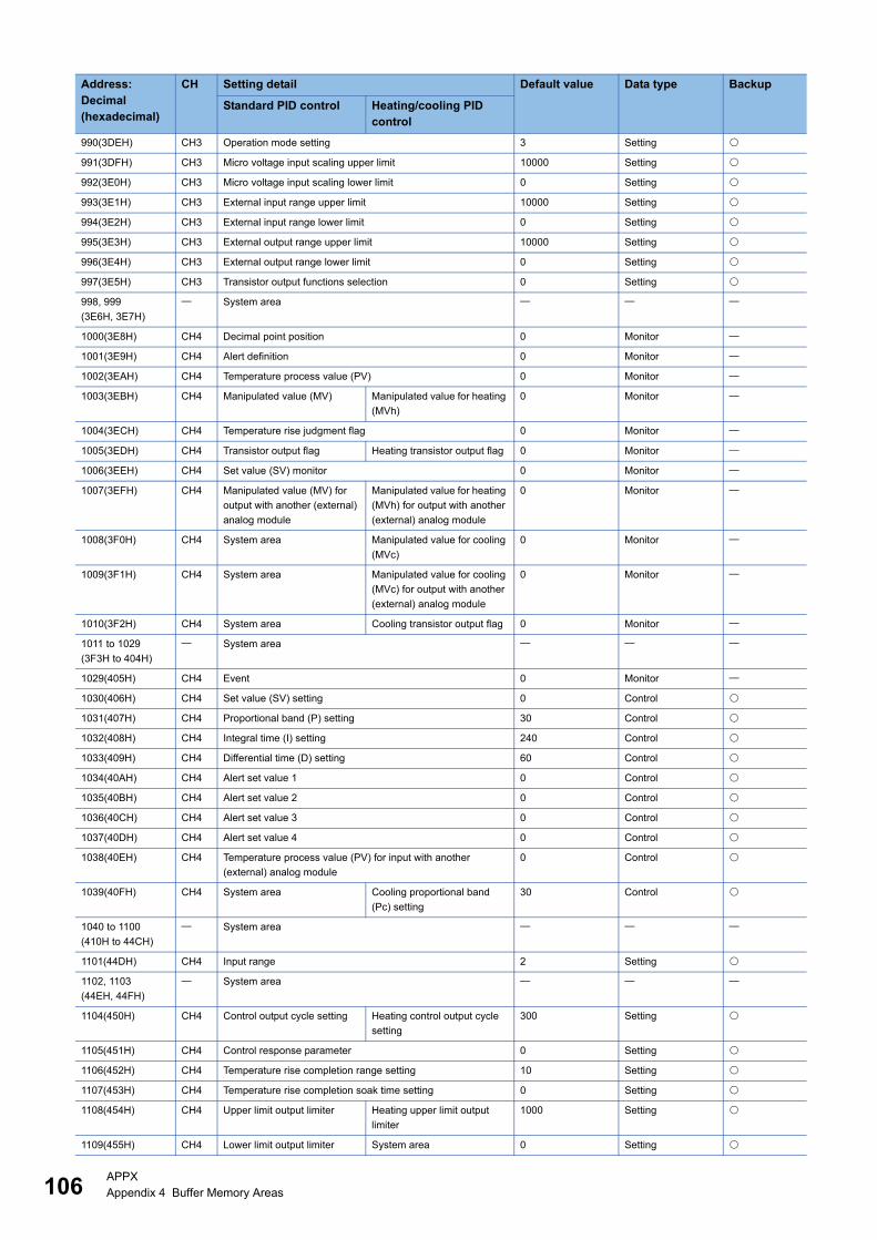
10
990(3DEH) CH3 Operation mode setting 3 Setting
991(3DFH) CH3 Micro voltage input scaling upper limit 10000 Setting
992(3E0H) CH3 Micro voltage input scaling lower limit 0 Setting
993(3E1H) CH3 External input range upper limit 10000 Setting
994(3E2H) CH3 External input range lower limit 0 Setting
995(3E3H) CH3 External output range upper limit 10000 Setting
996(3E4H) CH3 External output range lower limit 0 Setting
997(3E5H) CH3 Transistor output functions selection 0 Setting
998, 999
(3E6H, 3E7H)
System area
1000(3E8H) CH4 Decimal point position 0 Monitor
1001(3E9H) CH4 Alert definition 0 Monitor
1002(3EAH) CH4 Temperature process value (PV) 0 Monitor
1003(3EBH) CH4 Manipulated value (MV) Manipulated value for heating
(MVh)
0 Monitor
1004(3ECH) CH4 Temperature rise judgment flag 0 Monitor
1005(3EDH) CH4 Transistor output flag Heating transistor output flag 0 Monitor
1006(3EEH) CH4 Set value (SV) monitor 0 Monitor
1007(3EFH) CH4 Manipulated value (MV) for
output with another (external)
analog module
Manipulated value for heating
(MVh) for output with another
(external) analog module
0 Monitor
1008(3F0H) CH4 System area Manipulated value for cooling
(MVc)
0 Monitor
1009(3F1H) CH4 System area Manipulated value for cooling
(MVc) for output with another
(external) analog module
0 Monitor
1010(3F2H) CH4 System area Cooling transistor output flag 0 Monitor
1011 to 1029
(3F3H to 404H)
System area
1029(405H) CH4 Event 0 Monitor
1030(406H) CH4 Set value (SV) setting 0 Control
1031(407H) CH4 Proportional band (P) setting 30 Control
1032(408H) CH4 Integral time (I) setting 240 Control
1033(409H) CH4 Differential time (D) setting 60 Control
1034(40AH) CH4 Alert set value 1 0 Control
1035(40BH) CH4 Alert set value 2 0 Control
1036(40CH) CH4 Alert set value 3 0 Control
1037(40DH) CH4 Alert set value 4 0 Control
1038(40EH) CH4 Temperature process value (PV) for input with another
(external) analog module
0 Control
1039(40FH) CH4 System area Cooling proportional band
(Pc) setting
30 Control
1040 to 1100
(410H to 44CH)
System area
1101(44DH) CH4 Input range 2 Setting
1102, 1103
(44EH, 44FH)
System area
1104(450H) CH4 Control output cycle setting Heating control output cycle
setting
300 Setting
1105(451H) CH4 Control response parameter 0 Setting
1106(452H) CH4 Temperature rise completion range setting 10 Setting
1107(453H) CH4 Temperature rise completion soak time setting 0 Setting
1108(454H) CH4 Upper limit output limiter Heating upper limit output
limiter
1000 Setting
1109(455H) CH4 Lower limit output limiter System area 0 Setting
Address: Decimal (hexadecimal)
CH Setting detail Default value Data type Backup
Standard PID control Heating/cooling PID control
6APPXAppendix 4 Buffer Memory Areas
A
1110(456H) CH4 Output change ratio limiter System area 0 Setting
1111(457H) CH4 Upper limit setting limiter 1300 Setting
1112(458H) CH4 Lower limit setting limiter -100 Setting
1113(459H) CH4 Setting variation rate limiter 0 Setting
1114(45AH) System area
1115(45BH) CH4 Normal Operation/Reverse
Operation Setting
System area 1 Setting
1116(45CH) CH4 Adjustment sensitivity (dead band) setting 10 Setting
1117(45DH) System area
1118(45EH) CH4 AUTO/MAN mode shift System area 0 Setting
1119(45FH) CH4 Manual output setting System area -50 Setting
1120(460H) System area
1121(461H) CH4 System area Cooling upper limit output
limiter
1000 Setting
1122(462H) CH4 System area Cooling control output cycle
setting
300 Setting
1123(463H) CH4 System area Cooling method setting 0 Setting
1124(464H) CH4 System area Overlap/dead band setting 0 Setting
1125 to 1130
(465H to 46AH)
System area
1131(46BH) CH4 Alert dead band setting 10 Setting
1132(46CH) CH4 Number of alert delay 0 Setting
1133(46DH) CH4 Alert 1 mode setting*1 0 Setting
1134(46EH) CH4 Alert 2 mode setting*1 0 Setting
1135(46FH) CH4 Alert 3 mode setting*1 0 Setting
1136(470H) CH4 Alert 4 mode setting*1 0 Setting
1137(471H) CH4 Loop disconnection detection
judgment time
System area 480 Setting
1138(472H) CH4 Loop disconnection detection
dead band
System area 0 Setting
1139 to 1145
(473H to 479H)
System area
1146(47AH) CH4 AT bias 0 Setting
1147(47BH) System area
1148(47CH) CH4 Startup tuning implementation
command
System area 0 Setting
1149 to 1162
(47DH to 48AH)
System area
1163(48BH) CH4 Primary delay digital filter setting 0 Setting
1164(48CH) System area
1165(48DH) CH4 Sensor correction value setting 0 Setting
1166 to 1189
(48EH to 4A5H)
System area
1190(4A6H) CH4 Operation mode setting 3 Setting
1191(4A7H) CH4 Micro voltage input scaling upper limit 10000 Setting
1192(4A8H) CH4 Micro voltage input scaling lower limit 0 Setting
1193(4A9H) CH4 External input range upper limit 10000 Setting
1194(4AAH) CH4 External input range lower limit 0 Setting
1195(4ABH) CH4 External output range upper limit 10000 Setting
1196(4ACH) CH4 External output range lower limit 0 Setting
1197(4ADH) CH4 Transistor output functions selection 0 Setting
1198 to 1999
(4AEH to 7CFH)
System area
Address: Decimal (hexadecimal)
CH Setting detail Default value Data type Backup
Standard PID control Heating/cooling PID control
APPXAppendix 4 Buffer Memory Areas 107
10
*1 Can be changed only in the setting mode.
2000(7D0H) All Heater disconnection/output off-time current error detection
delay count
3 Setting
2001(7D1H) System area
2002(7D2H) All CT monitor method switching 0 Setting
2003(7D3H) System area
2004(7D4H) CH1 Heater disconnection alert setting 0 Setting
2005, 2006
(7D5H, 7D6H)
System area
2007(7D7H) CH2 Heater disconnection alert setting 0 Setting
2008, 2009
(7D8H, 7D9H)
System area
2010(7DAH) CH3 Heater disconnection alert
setting
System area 0 Setting
2011, 2012
(7DBH, 7DCH)
System area
2013(7DDH) CH4 Heater disconnection alert
setting
System area 0 Setting
2014 to 2029
(7DFH to 7EDH)
System area
2030(7EEH) CT1 Heater current process value 0 Monitor
2031(7EFH) CT2 Heater current process value 0 Monitor
2032(7F0H) CT3 Heater current process value 0 Monitor
2033(7F1H) CT4 Heater current process value 0 Monitor
2034 to 2061
(7F2H to 80DH)
System area
2062(80EH) CT1 CT ratio setting 800 Setting
2063(80FH) CT2 CT ratio setting 800 Setting
2064(810H) CT3 CT ratio setting 800 Setting
2065(811H) CT4 CT ratio setting 800 Setting
2066 to 3599
(812H to E0FH)
System area
3600 to 3759
(E10H to EAFH)
All Error history 0 Monitor
3760 to 3919
(EB0H to F4FH)
All Alarm history 0 Monitor
Address: Decimal (hexadecimal)
CH Setting detail Default value Data type Backup
Standard PID control Heating/cooling PID control
8APPXAppendix 4 Buffer Memory Areas
A
If using FX3 allocation modeThe following table describes the list of buffer memory addresses.
■Un\G0 to Un\G4095
Address: Decimal (hexadecimal)
CH Setting detail Monitor/Settings/Selection range
Default value
Data type Backup
Standard PID control
Heating/cooling PID control
0(0H) Flag Page 123 Monitor
1(1H) CH1 Event Page 134 Monitor
2(2H) CH2
3(3H) CH3
4(4H) CH4
5(5H) CH1 Measurement value (PV) input range span ±5% Monitor
6(6H) CH2
7(7H) CH3
8(8H) CH4
9(9H) CH1 Manipulated value
(control output value)
(MV) monitor
Manipulated value for
heating (heating control
output value) (MV)
monitor
-5.0 to +105.0% Monitor
10(AH) CH2
11(BH) CH3
12(CH) CH4
13(DH) CH1 System area Manipulated value for
cooling (MV) monitor
Normally 0 Monitor
14(EH) CH2
15(FH) CH3 0.0 to 105.0%
-5.0 displayed when control is
stopped
Monitor
16(10H) CH4
17(11H) CH1 Transistor output flag
(Control output flag)
Page 131 Monitor
18(12H) CH2
19(13H) CH3
20(14H) CH4
21(15H) CH1 Heater current process value 0.0 to 105.0 A Monitor
22(16H) CH2
23(17H) CH3
24(18H) CH4
25(19H) CH1 Temperature process value for input with another
(external) analog module
-32768 to +32767 0 Control
26(1AH) CH2
27(1BH) CH3
28(1CH) CH4
29(1DH) All Control start/stop switching 0: Control stop
1: Control start
0 Control
30(1EH) All Module information 61C2H 61C2H Monitor
31(1FH) All Firmware version 1000 1000 Monitor
32(20H) CH1 Manipulated value
(MV) for output with
another (external)
analog module monitor
Manipulated value
(MVh) for heating for
output with another
(external) analog
module monitor
External output range lower
limit to upper limit
0 Monitor
33(21H) CH2
34(22H) CH3
35(23H) CH4
36(24H) CH1 System area Manipulated value
(MVc) for cooling for
output with another
(external) analog
module monitor
0 Monitor
37(25H) CH2
38(26H) CH3
39(27H) CH4
40(28H) CH1 Set value (SV) monitor Lower limit setting limiter to
upper limit setting limiter
0 Monitor
41(29H) CH2
42(2AH) CH3
43(2BH) CH4
APPXAppendix 4 Buffer Memory Areas 109
11
44(2CH) CH1 Control mode monitor b0 to 2: Control mode
b15: Cascade control
implementation status
0 Monitor
45(2DH) CH2
46(2EH) CH3
47(2FH) CH4
48(30H) CH1 Set value (SV) setting Within setting limiter range 0 Control
49(31H) CH1 Alert 1 set value Depends on alert mode and
input type
0 Control
50(32H) CH1 Alert 2 set value Depends on alert mode and
input type
0 Control
51(33H) CH1 Alert 3 set value Depends on alert mode and
input type
0 Control
52(34H) CH1 Alert 4 set value Depends on alert mode and
input type
0 Control
53(35H) CH1 Heater disconnection alert setting 0 to 1000 (0.0 to 100.0 A) (0:
Heater disconnection
detection function OFF)
0 Control
54(36H) CH1 AUTO/MAN mode
switching
System area 0: AUTO
1: MAN
0 Setting
55(37H) CH1 Manual output settings System area -50 to +1050 -50/0 Setting
56(38H) CH1 AT (auto tuning) implementation command 0: Stop AT
1: Implement AT
0 Normal
57(39H) CH1 Operation mode setting 0: Not used
1: Monitor only
2: Monitor + alert
3: Monitor + alert + control
3 Setting
58(3AH) CH1 Proportional band (P)
setting
Heating proportional
band (P) setting
0 to 10000 (0.1 to 1000.0%
span)
Set 0 to use position 2
controls.
30 Control
59(3BH) CH1 System area Cooling proportional
band setting
1 to 10000 (0.1 to 1000.0%
span)
30 Control
60(3CH) CH1 Integral time (I) setting 0 to 3600s 240 Control
61(3DH) CH1 Differential time (D) setting 0 to 3600s 60 Control
62(3EH) CH1 Control response parameter 0: Slow
1: Regular
2: Fast
0 Setting
63(3FH) CH1 System area Overlap/dead band -100 to +100 0 Setting
64(40H) CH1 Upper limit output
limiter
Heating upper limit
output limiter
Lower limit output limiter +1 to
1050/0 to 1050
1000 Setting
65(41H) CH1 Lower limit output
limiter
System area -50 to upper limit output limiter
-1
0 Setting
66(42H) CH1 System area Cooling upper limit
output limiter
0 Setting
67(43H) CH1 Output change ratio
limiter
System area 0 to 1000 0 Setting
68(44H) CH1 Sensor correction value setting -5000 to +5000 0 Setting
69(45H) CH1 Controller sensitivity (dead band) setting 0 to 100 10 Setting
70(46H) CH1 Control output cycle
setting
Heating control output
cycle setting
5 to 1000 (0.5 to 100.0s) 300 Setting
71(47H) CH1 System area Cooling control output
cycle setting
5 to 1000 (0.5 to 100.0s) 0/300 Setting
72(48H) CH1 Primary delay digital filter setting 0 to 100s (0: Function OFF) 0 Setting
73(49H) CH1 Setting variation rate limiter 0 to 1000 0 Setting
74(4AH) CH1 AT bias ±Input span [, , digit] 0 Setting
75(4BH) CH1 Normal Operation/
Reverse Operation
Setting
System area 0: Normal Operation
1: Reverse Operation
1/0 Setting
Address: Decimal (hexadecimal)
CH Setting detail Monitor/Settings/Selection range
Default value
Data type Backup
Standard PID control
Heating/cooling PID control
0APPXAppendix 4 Buffer Memory Areas
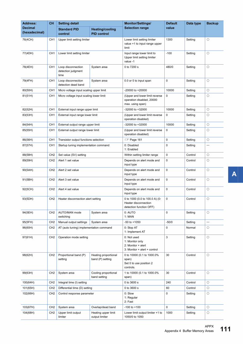
A
76(4CH) CH1 Upper limit setting limiter Lower limit setting limiter
value +1 to input range upper
limit
1300 Setting
77(4DH) CH1 Lower limit setting limiter Input range lower limit to
Upper limit setting limiter
value -1
-100 Setting
78(4EH) CH1 Loop disconnection
detection judgment
time
System area 0 to 7200 s 480/0 Setting
79(4FH) CH1 Loop disconnection
detection dead band
System area 0.0 or 0 to input span 0 Setting
80(50H) CH1 Micro voltage input scaling upper limit -20000 to +20000 10000 Setting
81(51H) CH1 Micro voltage input scaling lower limit (Upper and lower limit reverse
operation disabled, 20000
max. using span)
0 Setting
82(52H) CH1 External input range upper limit -32000 to +32000 10000 Setting
83(53H) CH1 External input range lower limit (Upper and lower limit reverse
operation disabled)
0 Setting
84(54H) CH1 External output range upper limit -32000 to +32000 10000 Setting
85(55H) CH1 External output range lower limit (Upper and lower limit reverse
operation disabled)
0 Setting
86(56H) CH1 Transistor output functions selection Page 161 0 Setting
87(57H) CH1 Startup tuning implementation command 0: Disabled
1: Enabled
0 Setting
88(58H) CH2 Set value (SV) setting Within setting limiter range 0 Control
89(59H) CH2 Alert 1 set value Depends on alert mode and
input type
0 Control
90(5AH) CH2 Alert 2 set value Depends on alert mode and
input type
0 Control
91(5BH) CH2 Alert 3 set value Depends on alert mode and
input type
0 Control
92(5CH) CH2 Alert 4 set value Depends on alert mode and
input type
0 Control
93(5DH) CH2 Heater disconnection alert setting 0 to 1000 (0.0 to 100.0 A) (0:
Heater disconnection
detection function OFF)
0 Control
94(5EH) CH2 AUTO/MAN mode
switching
System area 0: AUTO
1: MAN
0 Setting
95(5FH) CH2 Manual output settings System area -50 to +1050 -50/0 Setting
96(60H) CH2 AT (auto tuning) implementation command 0: Stop AT
1: Implement AT
0 Normal
97(61H) CH2 Operation mode setting 0: Not used
1: Monitor only
2: Monitor + alert
3: Monitor + alert + control
3 Setting
98(62H) CH2 Proportional band (P)
setting
Heating proportional
band (P) setting
0 to 10000 (0.1 to 1000.0%
span)
Set 0 to use position 2
controls.
30 Control
99(63H) CH2 System area Cooling proportional
band setting
1 to 10000 (0.1 to 1000.0%
span)
30 Control
100(64H) CH2 Integral time (I) setting 0 to 3600 s 240 Control
101(65H) CH2 Differential time (D) setting 0 to 3600 s 60 Control
102(66H) CH2 Control response parameter 0: Slow
1: Regular
2: Fast
0 Setting
103(67H) CH2 System area Overlap/dead band -100 to +100 0 Setting
104(68H) CH2 Upper limit output
limiter
Heating upper limit
output limiter
Lower limit output limiter +1 to
1050/0 to 1050
1000 Setting
Address: Decimal (hexadecimal)
CH Setting detail Monitor/Settings/Selection range
Default value
Data type Backup
Standard PID control
Heating/cooling PID control
APPXAppendix 4 Buffer Memory Areas 111
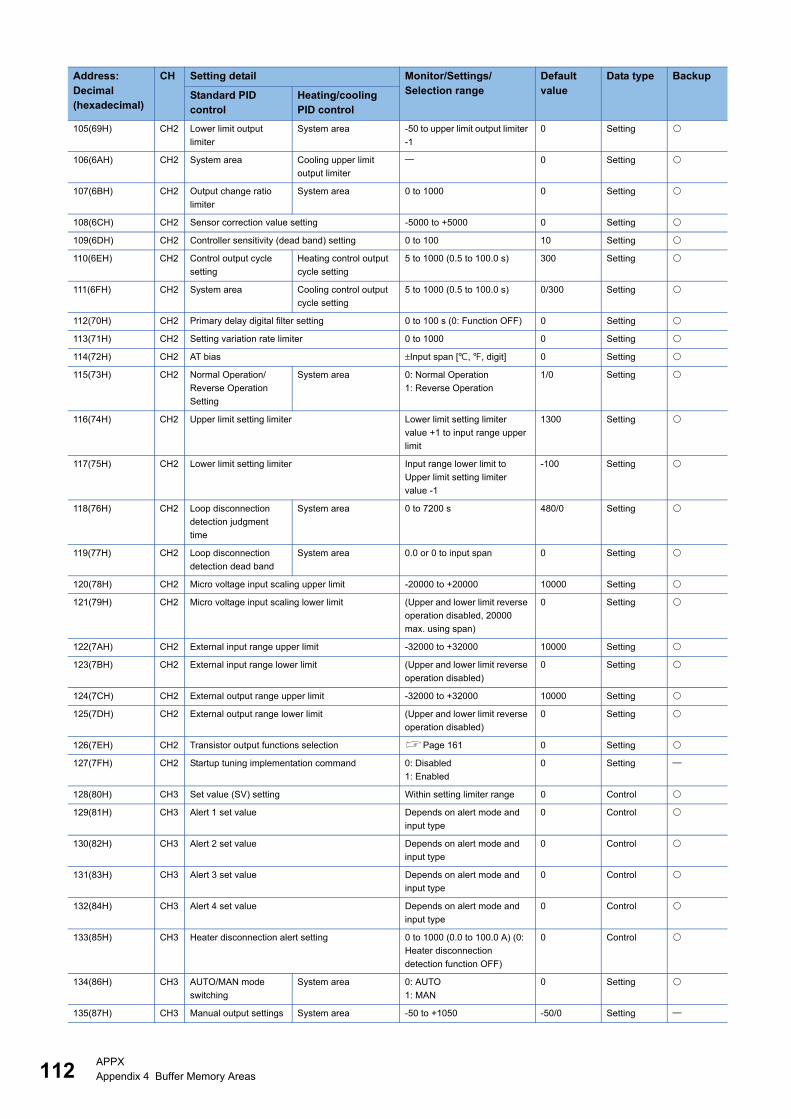
11
105(69H) CH2 Lower limit output
limiter
System area -50 to upper limit output limiter
-1
0 Setting
106(6AH) CH2 System area Cooling upper limit
output limiter
0 Setting
107(6BH) CH2 Output change ratio
limiter
System area 0 to 1000 0 Setting
108(6CH) CH2 Sensor correction value setting -5000 to +5000 0 Setting
109(6DH) CH2 Controller sensitivity (dead band) setting 0 to 100 10 Setting
110(6EH) CH2 Control output cycle
setting
Heating control output
cycle setting
5 to 1000 (0.5 to 100.0 s) 300 Setting
111(6FH) CH2 System area Cooling control output
cycle setting
5 to 1000 (0.5 to 100.0 s) 0/300 Setting
112(70H) CH2 Primary delay digital filter setting 0 to 100 s (0: Function OFF) 0 Setting
113(71H) CH2 Setting variation rate limiter 0 to 1000 0 Setting
114(72H) CH2 AT bias ±Input span [, , digit] 0 Setting
115(73H) CH2 Normal Operation/
Reverse Operation
Setting
System area 0: Normal Operation
1: Reverse Operation
1/0 Setting
116(74H) CH2 Upper limit setting limiter Lower limit setting limiter
value +1 to input range upper
limit
1300 Setting
117(75H) CH2 Lower limit setting limiter Input range lower limit to
Upper limit setting limiter
value -1
-100 Setting
118(76H) CH2 Loop disconnection
detection judgment
time
System area 0 to 7200 s 480/0 Setting
119(77H) CH2 Loop disconnection
detection dead band
System area 0.0 or 0 to input span 0 Setting
120(78H) CH2 Micro voltage input scaling upper limit -20000 to +20000 10000 Setting
121(79H) CH2 Micro voltage input scaling lower limit (Upper and lower limit reverse
operation disabled, 20000
max. using span)
0 Setting
122(7AH) CH2 External input range upper limit -32000 to +32000 10000 Setting
123(7BH) CH2 External input range lower limit (Upper and lower limit reverse
operation disabled)
0 Setting
124(7CH) CH2 External output range upper limit -32000 to +32000 10000 Setting
125(7DH) CH2 External output range lower limit (Upper and lower limit reverse
operation disabled)
0 Setting
126(7EH) CH2 Transistor output functions selection Page 161 0 Setting
127(7FH) CH2 Startup tuning implementation command 0: Disabled
1: Enabled
0 Setting
128(80H) CH3 Set value (SV) setting Within setting limiter range 0 Control
129(81H) CH3 Alert 1 set value Depends on alert mode and
input type
0 Control
130(82H) CH3 Alert 2 set value Depends on alert mode and
input type
0 Control
131(83H) CH3 Alert 3 set value Depends on alert mode and
input type
0 Control
132(84H) CH3 Alert 4 set value Depends on alert mode and
input type
0 Control
133(85H) CH3 Heater disconnection alert setting 0 to 1000 (0.0 to 100.0 A) (0:
Heater disconnection
detection function OFF)
0 Control
134(86H) CH3 AUTO/MAN mode
switching
System area 0: AUTO
1: MAN
0 Setting
135(87H) CH3 Manual output settings System area -50 to +1050 -50/0 Setting
Address: Decimal (hexadecimal)
CH Setting detail Monitor/Settings/Selection range
Default value
Data type Backup
Standard PID control
Heating/cooling PID control
2APPXAppendix 4 Buffer Memory Areas
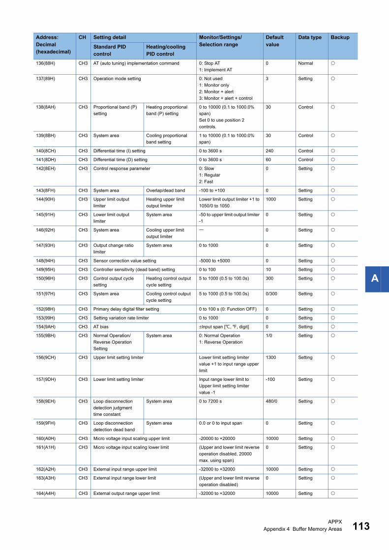
A
136(88H) CH3 AT (auto tuning) implementation command 0: Stop AT
1: Implement AT
0 Normal
137(89H) CH3 Operation mode setting 0: Not used
1: Monitor only
2: Monitor + alert
3: Monitor + alert + control
3 Setting
138(8AH) CH3 Proportional band (P)
setting
Heating proportional
band (P) setting
0 to 10000 (0.1 to 1000.0%
span)
Set 0 to use position 2
controls.
30 Control
139(8BH) CH3 System area Cooling proportional
band setting
1 to 10000 (0.1 to 1000.0%
span)
30 Control
140(8CH) CH3 Differential time (I) setting 0 to 3600 s 240 Control
141(8DH) CH3 Differential time (D) setting 0 to 3600 s 60 Control
142(8EH) CH3 Control response parameter 0: Slow
1: Regular
2: Fast
0 Setting
143(8FH) CH3 System area Overlap/dead band -100 to +100 0 Setting
144(90H) CH3 Upper limit output
limiter
Heating upper limit
output limiter
Lower limit output limiter +1 to
1050/0 to 1050
1000 Setting
145(91H) CH3 Lower limit output
limiter
System area -50 to upper limit output limiter
-1
0 Setting
146(92H) CH3 System area Cooling upper limit
output limiter
0 Setting
147(93H) CH3 Output change ratio
limiter
System area 0 to 1000 0 Setting
148(94H) CH3 Sensor correction value setting -5000 to +5000 0 Setting
149(95H) CH3 Controller sensitivity (dead band) setting 0 to 100 10 Setting
150(96H) CH3 Control output cycle
setting
Heating control output
cycle setting
5 to 1000 (0.5 to 100.0s) 300 Setting
151(97H) CH3 System area Cooling control output
cycle setting
5 to 1000 (0.5 to 100.0s) 0/300 Setting
152(98H) CH3 Primary delay digital filter setting 0 to 100 s (0: Function OFF) 0 Setting
153(99H) CH3 Setting variation rate limiter 0 to 1000 0 Setting
154(9AH) CH3 AT bias ±Input span [, , digit] 0 Setting
155(9BH) CH3 Normal Operation/
Reverse Operation
Setting
System area 0: Normal Operation
1: Reverse Operation
1/0 Setting
156(9CH) CH3 Upper limit setting limiter Lower limit setting limiter
value +1 to input range upper
limit
1300 Setting
157(9DH) CH3 Lower limit setting limiter Input range lower limit to
Upper limit setting limiter
value -1
-100 Setting
158(9EH) CH3 Loop disconnection
detection judgment
time constant
System area 0 to 7200 s 480/0 Setting
159(9FH) CH3 Loop disconnection
detection dead band
System area 0.0 or 0 to input span 0 Setting
160(A0H) CH3 Micro voltage input scaling upper limit -20000 to +20000 10000 Setting
161(A1H) CH3 Micro voltage input scaling lower limit (Upper and lower limit reverse
operation disabled, 20000
max. using span)
0 Setting
162(A2H) CH3 External input range upper limit -32000 to +32000 10000 Setting
163(A3H) CH3 External input range lower limit (Upper and lower limit reverse
operation disabled)
0 Setting
164(A4H) CH3 External output range upper limit -32000 to +32000 10000 Setting
Address: Decimal (hexadecimal)
CH Setting detail Monitor/Settings/Selection range
Default value
Data type Backup
Standard PID control
Heating/cooling PID control
APPXAppendix 4 Buffer Memory Areas 113
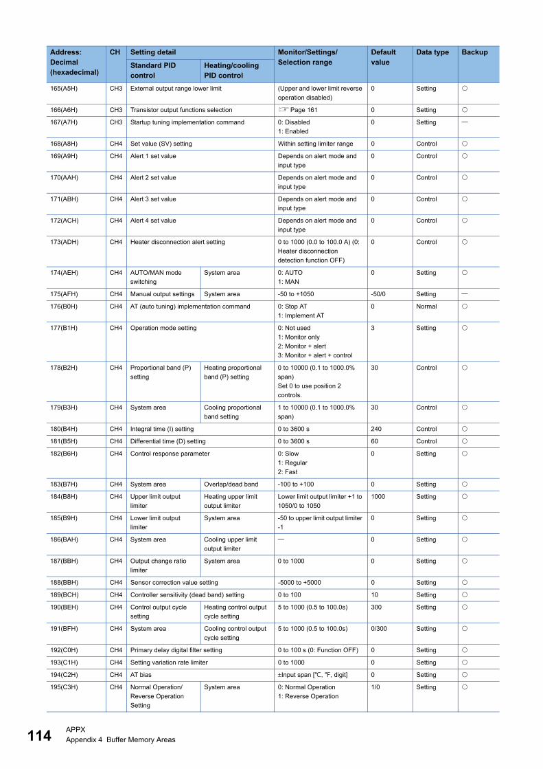
11
165(A5H) CH3 External output range lower limit (Upper and lower limit reverse
operation disabled)
0 Setting
166(A6H) CH3 Transistor output functions selection Page 161 0 Setting
167(A7H) CH3 Startup tuning implementation command 0: Disabled
1: Enabled
0 Setting
168(A8H) CH4 Set value (SV) setting Within setting limiter range 0 Control
169(A9H) CH4 Alert 1 set value Depends on alert mode and
input type
0 Control
170(AAH) CH4 Alert 2 set value Depends on alert mode and
input type
0 Control
171(ABH) CH4 Alert 3 set value Depends on alert mode and
input type
0 Control
172(ACH) CH4 Alert 4 set value Depends on alert mode and
input type
0 Control
173(ADH) CH4 Heater disconnection alert setting 0 to 1000 (0.0 to 100.0 A) (0:
Heater disconnection
detection function OFF)
0 Control
174(AEH) CH4 AUTO/MAN mode
switching
System area 0: AUTO
1: MAN
0 Setting
175(AFH) CH4 Manual output settings System area -50 to +1050 -50/0 Setting
176(B0H) CH4 AT (auto tuning) implementation command 0: Stop AT
1: Implement AT
0 Normal
177(B1H) CH4 Operation mode setting 0: Not used
1: Monitor only
2: Monitor + alert
3: Monitor + alert + control
3 Setting
178(B2H) CH4 Proportional band (P)
setting
Heating proportional
band (P) setting
0 to 10000 (0.1 to 1000.0%
span)
Set 0 to use position 2
controls.
30 Control
179(B3H) CH4 System area Cooling proportional
band setting
1 to 10000 (0.1 to 1000.0%
span)
30 Control
180(B4H) CH4 Integral time (I) setting 0 to 3600 s 240 Control
181(B5H) CH4 Differential time (D) setting 0 to 3600 s 60 Control
182(B6H) CH4 Control response parameter 0: Slow
1: Regular
2: Fast
0 Setting
183(B7H) CH4 System area Overlap/dead band -100 to +100 0 Setting
184(B8H) CH4 Upper limit output
limiter
Heating upper limit
output limiter
Lower limit output limiter +1 to
1050/0 to 1050
1000 Setting
185(B9H) CH4 Lower limit output
limiter
System area -50 to upper limit output limiter
-1
0 Setting
186(BAH) CH4 System area Cooling upper limit
output limiter
0 Setting
187(BBH) CH4 Output change ratio
limiter
System area 0 to 1000 0 Setting
188(BBH) CH4 Sensor correction value setting -5000 to +5000 0 Setting
189(BCH) CH4 Controller sensitivity (dead band) setting 0 to 100 10 Setting
190(BEH) CH4 Control output cycle
setting
Heating control output
cycle setting
5 to 1000 (0.5 to 100.0s) 300 Setting
191(BFH) CH4 System area Cooling control output
cycle setting
5 to 1000 (0.5 to 100.0s) 0/300 Setting
192(C0H) CH4 Primary delay digital filter setting 0 to 100 s (0: Function OFF) 0 Setting
193(C1H) CH4 Setting variation rate limiter 0 to 1000 0 Setting
194(C2H) CH4 AT bias ±Input span [, , digit] 0 Setting
195(C3H) CH4 Normal Operation/
Reverse Operation
Setting
System area 0: Normal Operation
1: Reverse Operation
1/0 Setting
Address: Decimal (hexadecimal)
CH Setting detail Monitor/Settings/Selection range
Default value
Data type Backup
Standard PID control
Heating/cooling PID control
4APPXAppendix 4 Buffer Memory Areas
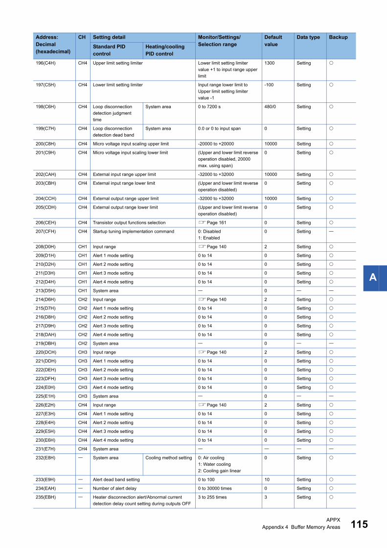
A
196(C4H) CH4 Upper limit setting limiter Lower limit setting limiter
value +1 to input range upper
limit
1300 Setting
197(C5H) CH4 Lower limit setting limiter Input range lower limit to
Upper limit setting limiter
value -1
-100 Setting
198(C6H) CH4 Loop disconnection
detection judgment
time
System area 0 to 7200 s 480/0 Setting
199(C7H) CH4 Loop disconnection
detection dead band
System area 0.0 or 0 to input span 0 Setting
200(C8H) CH4 Micro voltage input scaling upper limit -20000 to +20000 10000 Setting
201(C9H) CH4 Micro voltage input scaling lower limit (Upper and lower limit reverse
operation disabled, 20000
max. using span)
0 Setting
202(CAH) CH4 External input range upper limit -32000 to +32000 10000 Setting
203(CBH) CH4 External input range lower limit (Upper and lower limit reverse
operation disabled)
0 Setting
204(CCH) CH4 External output range upper limit -32000 to +32000 10000 Setting
205(CDH) CH4 External output range lower limit (Upper and lower limit reverse
operation disabled)
0 Setting
206(CEH) CH4 Transistor output functions selection Page 161 0 Setting
207(CFH) CH4 Startup tuning implementation command 0: Disabled
1: Enabled
0 Setting
208(D0H) CH1 Input range Page 140 2 Setting
209(D1H) CH1 Alert 1 mode setting 0 to 14 0 Setting
210(D2H) CH1 Alert 2 mode setting 0 to 14 0 Setting
211(D3H) CH1 Alert 3 mode setting 0 to 14 0 Setting
212(D4H) CH1 Alert 4 mode setting 0 to 14 0 Setting
213(D5H) CH1 System area 0
214(D6H) CH2 Input range Page 140 2 Setting
215(D7H) CH2 Alert 1 mode setting 0 to 14 0 Setting
216(D8H) CH2 Alert 2 mode setting 0 to 14 0 Setting
217(D9H) CH2 Alert 3 mode setting 0 to 14 0 Setting
218(DAH) CH2 Alert 4 mode setting 0 to 14 0 Setting
219(DBH) CH2 System area 0
220(DCH) CH3 Input range Page 140 2 Setting
221(DDH) CH3 Alert 1 mode setting 0 to 14 0 Setting
222(DEH) CH3 Alert 2 mode setting 0 to 14 0 Setting
223(DFH) CH3 Alert 3 mode setting 0 to 14 0 Setting
224(E0H) CH3 Alert 4 mode setting 0 to 14 0 Setting
225(E1H) CH3 System area 0
226(E2H) CH4 Input range Page 140 2 Setting
227(E3H) CH4 Alert 1 mode setting 0 to 14 0 Setting
228(E4H) CH4 Alert 2 mode setting 0 to 14 0 Setting
229(E5H) CH4 Alert 3 mode setting 0 to 14 0 Setting
230(E6H) CH4 Alert 4 mode setting 0 to 14 0 Setting
231(E7H) CH4 System area
232(E8H) System area Cooling method setting 0: Air cooling
1: Water cooling
2: Cooling gain linear
0 Setting
233(E9H) Alert dead band setting 0 to 100 10 Setting
234(EAH) Number of alert delay 0 to 30000 times 0 Setting
235(EBH) Heater disconnection alert/Abnormal current
detection delay count setting during outputs OFF
3 to 255 times 3 Setting
Address: Decimal (hexadecimal)
CH Setting detail Monitor/Settings/Selection range
Default value
Data type Backup
Standard PID control
Heating/cooling PID control
APPXAppendix 4 Buffer Memory Areas 115
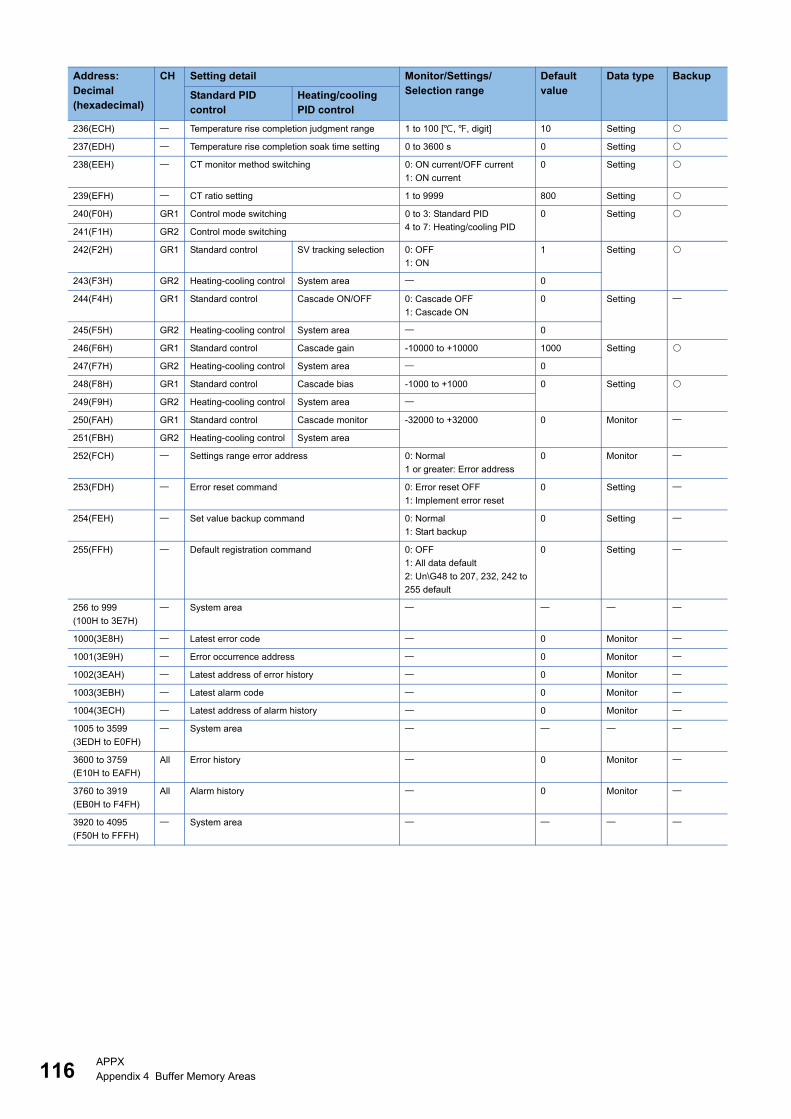
11
236(ECH) Temperature rise completion judgment range 1 to 100 [, , digit] 10 Setting
237(EDH) Temperature rise completion soak time setting 0 to 3600 s 0 Setting
238(EEH) CT monitor method switching 0: ON current/OFF current
1: ON current
0 Setting
239(EFH) CT ratio setting 1 to 9999 800 Setting
240(F0H) GR1 Control mode switching 0 to 3: Standard PID
4 to 7: Heating/cooling PID
0 Setting
241(F1H) GR2 Control mode switching
242(F2H) GR1 Standard control SV tracking selection 0: OFF
1: ON
1 Setting
243(F3H) GR2 Heating-cooling control System area 0
244(F4H) GR1 Standard control Cascade ON/OFF 0: Cascade OFF
1: Cascade ON
0 Setting
245(F5H) GR2 Heating-cooling control System area 0
246(F6H) GR1 Standard control Cascade gain -10000 to +10000 1000 Setting
247(F7H) GR2 Heating-cooling control System area 0
248(F8H) GR1 Standard control Cascade bias -1000 to +1000 0 Setting
249(F9H) GR2 Heating-cooling control System area
250(FAH) GR1 Standard control Cascade monitor -32000 to +32000 0 Monitor
251(FBH) GR2 Heating-cooling control System area
252(FCH) Settings range error address 0: Normal
1 or greater: Error address
0 Monitor
253(FDH) Error reset command 0: Error reset OFF
1: Implement error reset
0 Setting
254(FEH) Set value backup command 0: Normal
1: Start backup
0 Setting
255(FFH) Default registration command 0: OFF
1: All data default
2: Un\G48 to 207, 232, 242 to
255 default
0 Setting
256 to 999
(100H to 3E7H)
System area
1000(3E8H) Latest error code 0 Monitor
1001(3E9H) Error occurrence address 0 Monitor
1002(3EAH) Latest address of error history 0 Monitor
1003(3EBH) Latest alarm code 0 Monitor
1004(3ECH) Latest address of alarm history 0 Monitor
1005 to 3599
(3EDH to E0FH)
System area
3600 to 3759
(E10H to EAFH)
All Error history 0 Monitor
3760 to 3919
(EB0H to F4FH)
All Alarm history 0 Monitor
3920 to 4095
(F50H to FFFH)
System area
Address: Decimal (hexadecimal)
CH Setting detail Monitor/Settings/Selection range
Default value
Data type Backup
Standard PID control
Heating/cooling PID control
6APPXAppendix 4 Buffer Memory Areas
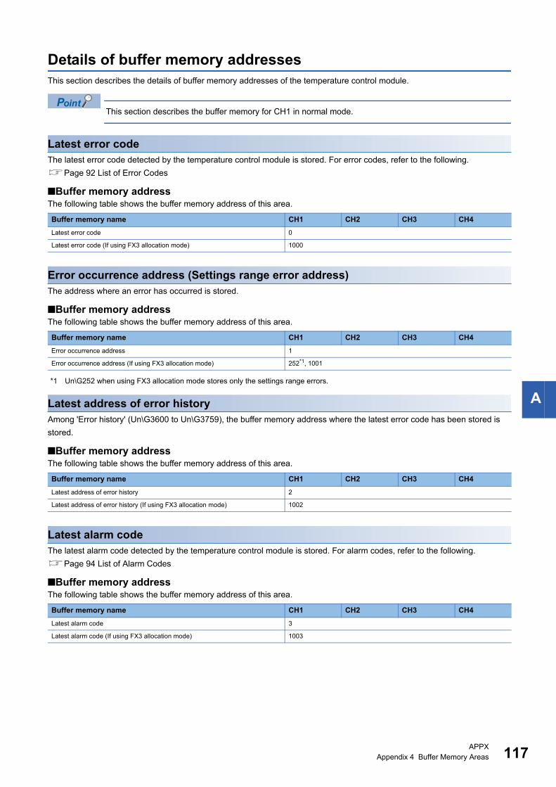
A
Details of buffer memory addressesThis section describes the details of buffer memory addresses of the temperature control module.
This section describes the buffer memory for CH1 in normal mode.
Latest error codeThe latest error code detected by the temperature control module is stored. For error codes, refer to the following.
Page 92 List of Error Codes
■Buffer memory addressThe following table shows the buffer memory address of this area.
Error occurrence address (Settings range error address)The address where an error has occurred is stored.
■Buffer memory addressThe following table shows the buffer memory address of this area.
*1 Un\G252 when using FX3 allocation mode stores only the settings range errors.
Latest address of error historyAmong 'Error history' (Un\G3600 to Un\G3759), the buffer memory address where the latest error code has been stored is
stored.
■Buffer memory addressThe following table shows the buffer memory address of this area.
Latest alarm codeThe latest alarm code detected by the temperature control module is stored. For alarm codes, refer to the following.
Page 94 List of Alarm Codes
■Buffer memory addressThe following table shows the buffer memory address of this area.
Buffer memory name CH1 CH2 CH3 CH4
Latest error code 0
Latest error code (If using FX3 allocation mode) 1000
Buffer memory name CH1 CH2 CH3 CH4
Error occurrence address 1
Error occurrence address (If using FX3 allocation mode) 252*1, 1001
Buffer memory name CH1 CH2 CH3 CH4
Latest address of error history 2
Latest address of error history (If using FX3 allocation mode) 1002
Buffer memory name CH1 CH2 CH3 CH4
Latest alarm code 3
Latest alarm code (If using FX3 allocation mode) 1003
APPXAppendix 4 Buffer Memory Areas 117
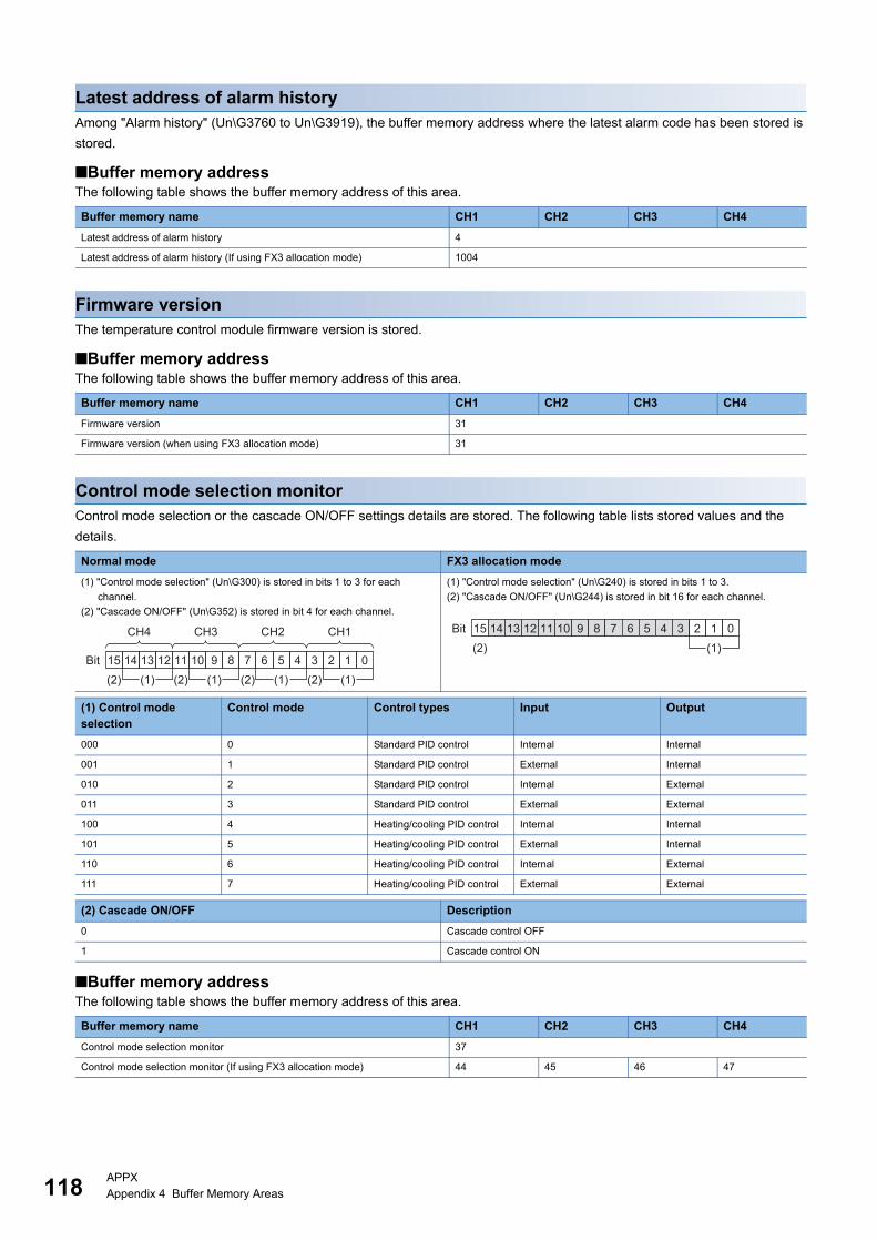
11
Latest address of alarm historyAmong "Alarm history" (Un\G3760 to Un\G3919), the buffer memory address where the latest alarm code has been stored is
stored.
■Buffer memory addressThe following table shows the buffer memory address of this area.
Firmware versionThe temperature control module firmware version is stored.
■Buffer memory addressThe following table shows the buffer memory address of this area.
Control mode selection monitorControl mode selection or the cascade ON/OFF settings details are stored. The following table lists stored values and the
details.
■Buffer memory addressThe following table shows the buffer memory address of this area.
Buffer memory name CH1 CH2 CH3 CH4
Latest address of alarm history 4
Latest address of alarm history (If using FX3 allocation mode) 1004
Buffer memory name CH1 CH2 CH3 CH4
Firmware version 31
Firmware version (when using FX3 allocation mode) 31
Normal mode FX3 allocation mode
(1) "Control mode selection" (Un\G300) is stored in bits 1 to 3 for each
channel.
(2) "Cascade ON/OFF" (Un\G352) is stored in bit 4 for each channel.
(1) "Control mode selection" (Un\G240) is stored in bits 1 to 3.
(2) "Cascade ON/OFF" (Un\G244) is stored in bit 16 for each channel.
(1) Control mode selection
Control mode Control types Input Output
000 0 Standard PID control Internal Internal
001 1 Standard PID control External Internal
010 2 Standard PID control Internal External
011 3 Standard PID control External External
100 4 Heating/cooling PID control Internal Internal
101 5 Heating/cooling PID control External Internal
110 6 Heating/cooling PID control Internal External
111 7 Heating/cooling PID control External External
(2) Cascade ON/OFF Description
0 Cascade control OFF
1 Cascade control ON
Buffer memory name CH1 CH2 CH3 CH4
Control mode selection monitor 37
Control mode selection monitor (If using FX3 allocation mode) 44 45 46 47
15Bit
CH4
(2) (1) (2) (1) (2) (1) (2) (1)
CH3 CH2 CH1
14 13 12 11 10 9 8 7 6 5 4 3 2 1 0
15Bit 14 13 12 11 10 9 8 7 6 5 4 3 2 1 0(2) (1)
8APPXAppendix 4 Buffer Memory Areas
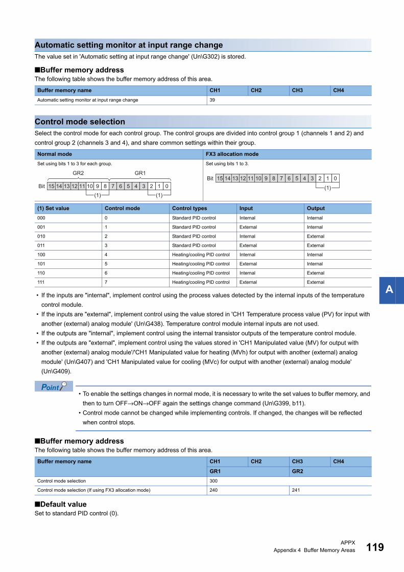
A
Automatic setting monitor at input range changeThe value set in 'Automatic setting at input range change' (Un\G302) is stored.
■Buffer memory addressThe following table shows the buffer memory address of this area.
Control mode selectionSelect the control mode for each control group. The control groups are divided into control group 1 (channels 1 and 2) and
control group 2 (channels 3 and 4), and share common settings within their group.
• If the inputs are "internal", implement control using the process values detected by the internal inputs of the temperature
control module.
• If the inputs are "external", implement control using the value stored in 'CH1 Temperature process value (PV) for input with
another (external) analog module' (Un\G438). Temperature control module internal inputs are not used.
• If the outputs are "internal", implement control using the internal transistor outputs of the temperature control module.
• If the outputs are "external", implement control using the values stored in 'CH1 Manipulated value (MV) for output with
another (external) analog module'/'CH1 Manipulated value for heating (MVh) for output with another (external) analog
module' (Un\G407) and 'CH1 Manipulated value for cooling (MVc) for output with another (external) analog module'
(Un\G409).
• To enable the settings changes in normal mode, it is necessary to write the set values to buffer memory, and
then to turn OFF→ON→OFF again the settings change command (Un\G399, b11).
• Control mode cannot be changed while implementing controls. If changed, the changes will be reflected
when control stops.
■Buffer memory addressThe following table shows the buffer memory address of this area.
■Default valueSet to standard PID control (0).
Buffer memory name CH1 CH2 CH3 CH4
Automatic setting monitor at input range change 39
Normal mode FX3 allocation mode
Set using bits 1 to 3 for each group. Set using bits 1 to 3.
(1) Set value Control mode Control types Input Output
000 0 Standard PID control Internal Internal
001 1 Standard PID control External Internal
010 2 Standard PID control Internal External
011 3 Standard PID control External External
100 4 Heating/cooling PID control Internal Internal
101 5 Heating/cooling PID control External Internal
110 6 Heating/cooling PID control Internal External
111 7 Heating/cooling PID control External External
Buffer memory name CH1 CH2 CH3 CH4
GR1 GR2
Control mode selection 300
Control mode selection (If using FX3 allocation mode) 240 241
15Bit
GR2 GR1
14 13 12 11 10 9 8 7 6 5 4 3 2 1 0(1) (1)
15Bit 14 13 12 11 10 9 8 7 6 5 4 3 2 1 0
(1)
APPXAppendix 4 Buffer Memory Areas 119
12
Automatic setting at input range changeWhen "Channel 1 input range" (Un\G501) is changed, this function automatically changes the relevant buffer memory data to
make sure that an outside settings range error (error code: 1950H) does not occur.
• 0: Disabled
• 1: Enabled
When Enable (1) has been set, the following buffer memory areas are automatically set or initialized when the setting of 'CH1
Input range' (Un\G501) is changed.
If changing the input range in normal mode, it is necessary to turn OFF→ON→OFF again the settings change
command (Un\G399, b11).
■Buffer memory addressThe following table shows the buffer memory address of this area.
■Default valueSet to disabled (0).
Buffer memory name Default value
Standard PID control Heating/cooling PID control
Set value (SV) setting (Un\G430) 0 0
(Heating) proportional band (Un\G431) 30 30
Alerts 1 to 4 settings (Un\G434 to 437) 0 0
(Cooling) proportional band (Un\G439) 30
Upper limit setting limiter (Un\G511) Upper limit value of the input range Upper limit value of the input range
Lower limit setting limiter (Un\G512) Lower limit value of the input range Lower limit value of the input range
Setting change rate limiter (Un\G513) 0 0
Adjustment sensitivity (dead band) setting
(Un\G516)
10 10
Overlap/dead band (Un\G524) 0
Alert dead band setting (Un\G531) 10 10
Loop disconnection detection dead band
(Un\G538)
0 0
AT bias (Un\G546) 0 0
Sensor compensation set value (Un\G565) 0 0
Buffer memory name CH1 CH2 CH3 CH4
Automatic setting at input range change 302
0APPXAppendix 4 Buffer Memory Areas
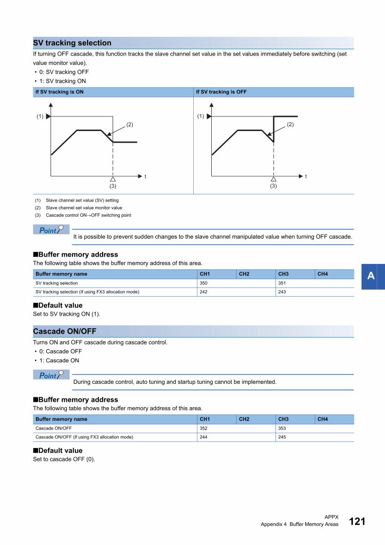
A
SV tracking selectionIf turning OFF cascade, this function tracks the slave channel set value in the set values immediately before switching (set
value monitor value).
• 0: SV tracking OFF
• 1: SV tracking ON
It is possible to prevent sudden changes to the slave channel manipulated value when turning OFF cascade.
■Buffer memory addressThe following table shows the buffer memory address of this area.
■Default valueSet to SV tracking ON (1).
Cascade ON/OFFTurns ON and OFF cascade during cascade control.
• 0: Cascade OFF
• 1: Cascade ON
During cascade control, auto tuning and startup tuning cannot be implemented.
■Buffer memory addressThe following table shows the buffer memory address of this area.
■Default valueSet to cascade OFF (0).
If SV tracking is ON If SV tracking is OFF
(1) Slave channel set value (SV) setting
(2) Slave channel set value monitor value
(3) Cascade control ON→OFF switching point
Buffer memory name CH1 CH2 CH3 CH4
SV tracking selection 350 351
SV tracking selection (If using FX3 allocation mode) 242 243
Buffer memory name CH1 CH2 CH3 CH4
Cascade ON/OFF 352 353
Cascade ON/OFF (If using FX3 allocation mode) 244 245
(1)(2)
(3)
t
(1)(2)
(3)
t
APPXAppendix 4 Buffer Memory Areas 121
12
Cascade gainDuring cascade control, gain is set when converting the master channel manipulated value (MV) to the cascade monitor
value.
■Buffer memory addressThe following table shows the buffer memory address of this area.
■Setting range Set to -10000 to +10000 (x-10.000 to x+10.000).
■Default value Set to 1000 (x1.000).
Cascade biasSets the bias amount that is added to the sum of the master channel manipulated value (MV) and cascade gain during
cascade control.
■Buffer memory addressThe following table shows the buffer memory address of this area.
■Setting range Set to -1000 to +1000 (-100.0 to +100.0%).
■Default valueThe default value is 0.
Cascade monitorStores the master manipulated value (cascade signal) converted using 'cascade gain' and 'cascade bias' that is added to the
slave set value during cascade control.
If 'cascade ON/OFF' is OFF (0), 0 is stored in the cascade monitor.
■Buffer memory addressThe following table shows the buffer memory address of this area.
Buffer memory name CH1 CH2 CH3 CH4
Cascade gain 354 355
Cascade gain (If using FX3 allocation mode) 246 247
Buffer memory name CH1 CH2 CH3 CH4
Cascade bias 356 357
Cascade bias (If using FX3 allocation mode) 248 249
Buffer memory name CH1 CH2 CH3 CH4
Cascade monitor 358 359
Cascade monitor (If using FX3 allocation mode) 250 251
2APPXAppendix 4 Buffer Memory Areas
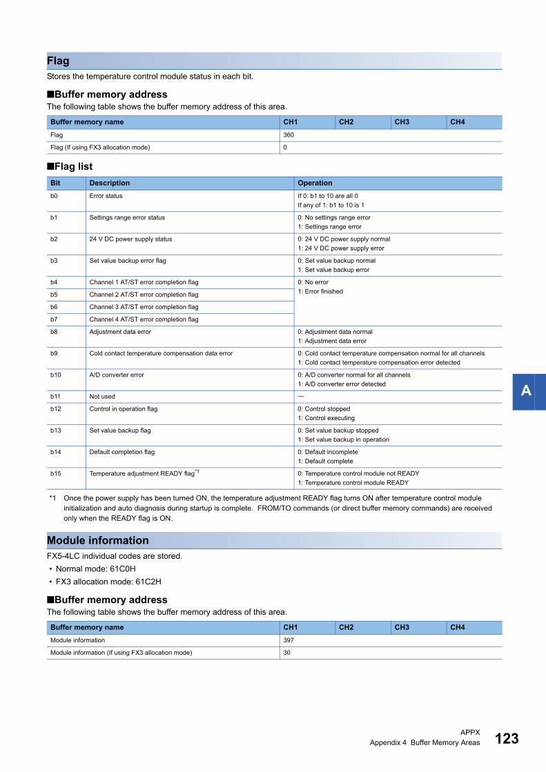
A
FlagStores the temperature control module status in each bit.
■Buffer memory addressThe following table shows the buffer memory address of this area.
■Flag list
*1 Once the power supply has been turned ON, the temperature adjustment READY flag turns ON after temperature control module initialization and auto diagnosis during startup is complete. FROM/TO commands (or direct buffer memory commands) are received only when the READY flag is ON.
Module informationFX5-4LC individual codes are stored.
• Normal mode: 61C0H
• FX3 allocation mode: 61C2H
■Buffer memory addressThe following table shows the buffer memory address of this area.
Buffer memory name CH1 CH2 CH3 CH4
Flag 360
Flag (If using FX3 allocation mode) 0
Bit Description Operation
b0 Error status If 0: b1 to 10 are all 0
If any of 1: b1 to 10 is 1
b1 Settings range error status 0: No settings range error
1: Settings range error
b2 24 V DC power supply status 0: 24 V DC power supply normal
1: 24 V DC power supply error
b3 Set value backup error flag 0: Set value backup normal
1: Set value backup error
b4 Channel 1 AT/ST error completion flag 0: No error
1: Error finishedb5 Channel 2 AT/ST error completion flag
b6 Channel 3 AT/ST error completion flag
b7 Channel 4 AT/ST error completion flag
b8 Adjustment data error 0: Adjustment data normal
1: Adjustment data error
b9 Cold contact temperature compensation data error 0: Cold contact temperature compensation normal for all channels
1: Cold contact temperature compensation error detected
b10 A/D converter error 0: A/D converter normal for all channels
1: A/D converter error detected
b11 Not used
b12 Control in operation flag 0: Control stopped
1: Control executing
b13 Set value backup flag 0: Set value backup stopped
1: Set value backup in operation
b14 Default completion flag 0: Default incomplete
1: Default complete
b15 Temperature adjustment READY flag*1 0: Temperature control module not READY
1: Temperature control module READY
Buffer memory name CH1 CH2 CH3 CH4
Module information 397
Module information (If using FX3 allocation mode) 30
APPXAppendix 4 Buffer Memory Areas 123
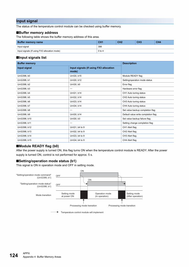
12
Input signalThe status of the temperature control module can be checked using buffer memory.
■Buffer memory addressThe following table shows the buffer memory address of this area.
■Input signals list
■Module READY flag (b0)After the power supply is turned ON, this flag turns ON when the temperature control module is READY. After the power
supply is turned ON, control is not performed for approx. 5 s.
■Setting/operation mode status (b1)This signal is ON in operation mode and OFF in setting mode.
Buffer memory name CH1 CH2 CH3 CH4
Input signal 398
Input signals (If using FX3 allocation mode) 0 to 4
Buffer memory Description
Input signal Input signals (If using FX3 allocation mode)
Un\G398, b0 Un\G0, b15 Module READY flag
Un\G398, b1 Un\G0, b12 Setting/operation mode status
Un\G398, b2 Un\G0, b0 Error flag
Un\G398, b3 Hardware error flag
Un\G398, b4 Un\G1, b14 CH1 Auto tuning status
Un\G398, b5 Un\G2, b14 CH2 Auto tuning status
Un\G398, b6 Un\G3, b14 CH3 Auto tuning status
Un\G398, b7 Un\G4, b14 CH4 Auto tuning status
Un\G398, b8 Set value backup completion flag
Un\G398, b9 Un\G0, b14 Default value write completion flag
Un\G398, b10 Un\G0, b3 Set value backup failure flag
Un\G398, b11 Setting change completion flag
Un\G398, b12 Un\G1, b4 to 9 CH1 Alert flag
Un\G398, b13 Un\G2, b4 to 9 CH2 Alert flag
Un\G398, b14 Un\G3, b4 to 9 CH3 Alert flag
Un\G398, b15 Un\G4, b4 to 9 CH4 Alert flag
ON
OFF
OFF
ON
"Setting/operation mode command"(Un\G399, b1)
"Setting/operation mode status"(Un\G398, b1)
Mode transition
Processing mode transition Processing mode transition
Setting mode(After operation)
Operation mode(In operation)
Temperature control module will implement
Setting mode at power ON
4APPXAppendix 4 Buffer Memory Areas
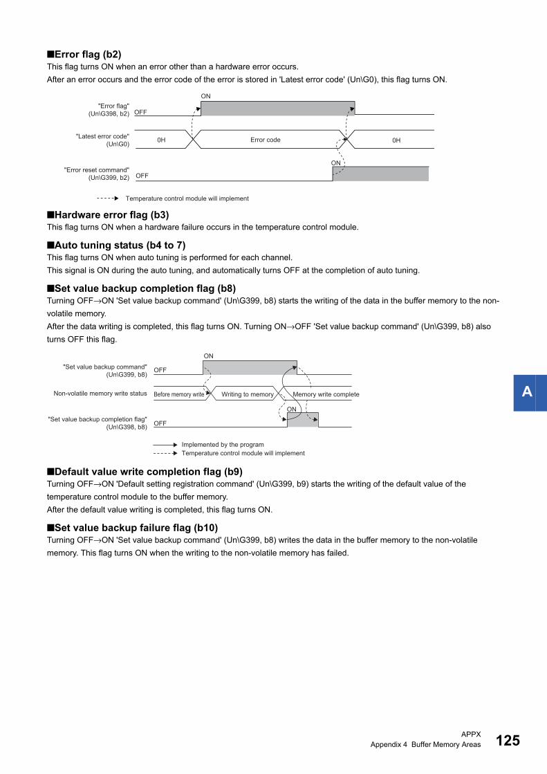
A
■Error flag (b2)This flag turns ON when an error other than a hardware error occurs.
After an error occurs and the error code of the error is stored in 'Latest error code' (Un\G0), this flag turns ON.
■Hardware error flag (b3)This flag turns ON when a hardware failure occurs in the temperature control module.
■Auto tuning status (b4 to 7)This flag turns ON when auto tuning is performed for each channel.
This signal is ON during the auto tuning, and automatically turns OFF at the completion of auto tuning.
■Set value backup completion flag (b8)Turning OFF→ON 'Set value backup command' (Un\G399, b8) starts the writing of the data in the buffer memory to the non-
volatile memory.
After the data writing is completed, this flag turns ON. Turning ON→OFF 'Set value backup command' (Un\G399, b8) also
turns OFF this flag.
■Default value write completion flag (b9)Turning OFF→ON 'Default setting registration command' (Un\G399, b9) starts the writing of the default value of the
temperature control module to the buffer memory.
After the default value writing is completed, this flag turns ON.
■Set value backup failure flag (b10)Turning OFF→ON 'Set value backup command' (Un\G399, b8) writes the data in the buffer memory to the non-volatile
memory. This flag turns ON when the writing to the non-volatile memory has failed.
OFF
OFF
ON
0H 0H
ON
"Error flag"(Un\G398, b2)
"Latest error code"(Un\G0)
"Error reset command"(Un\G399, b2)
Error code
Temperature control module will implement
ON
OFF
ON
OFF
Before memory write Writing to memory Memory write complete
"Set value backup command"(Un\G399, b8)
Non-volatile memory write status
"Set value backup completion flag"(Un\G398, b8)
Implemented by the programTemperature control module will implement
APPXAppendix 4 Buffer Memory Areas 125
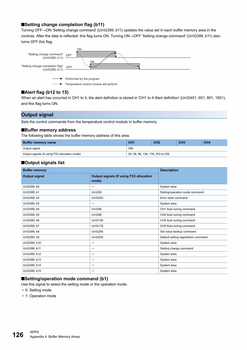
12
■Setting change completion flag (b11)Turning OFF→ON 'Setting change command' (Un\G399, b11) updates the value set in each buffer memory area in the
controls. After the data is reflected, this flag turns ON. Turning ON→OFF 'Setting change command' (Un\G399, b11) also
turns OFF this flag.
■Alert flag (b12 to 15)When an alert has occurred in CH1 to 4, the alert definition is stored in 'CH1 to 4 Alert definition' (Un\G401, 601, 801, 1001),
and this flag turns ON.
Output signalSets the control commands from the temperature control module in buffer memory.
■Buffer memory addressThe following table shows the buffer memory address of this area.
■Output signals list
■Setting/operation mode command (b1)Use this signal to select the setting mode or the operation mode.
• 0: Setting mode
• 1: Operation mode
Buffer memory name CH1 CH2 CH3 CH4
Output signal 399
Output signals (If using FX3 allocation mode) 29, 56, 96, 136, 176, 253 to 255
Buffer memory Description
Output signal Output signals (If using FX3 allocation mode)
Un\G399, b0 System area
Un\G399, b1 Un\G29 Setting/operation mode command
Un\G399, b2 Un\G253 Error reset command
Un\G399, b3 System area
Un\G399, b4 Un\G56 CH1 Auto tuning command
Un\G399, b5 Un\G96 CH2 Auto tuning command
Un\G399, b6 Un\G136 CH3 Auto tuning command
Un\G399, b7 Un\G176 CH4 Auto tuning command
Un\G399, b8 Un\G254 Set value backup command
Un\G399, b9 Un\G255 Default setting registration command
Un\G399, b10 System area
Un\G399, b11 Setting change command
Un\G399, b12 System area
Un\G399, b13 System area
Un\G399, b14 System area
Un\G399, b15 System area
ON
OFF
OFF
ON
"Setting change command"(Un\G399, b11)
"Setting change completion flag"(Un\G398, b11)
Performed by the program
Temperature control module will perform
6APPXAppendix 4 Buffer Memory Areas
A
■Error reset command (b2)Turning OFF→ON the error reset command resets the following information.
• Latest error code
• Error occurrence address (Settings range error address)
• Latest alarm code
• Input signals error occurrence flag (Un\G398, b2)
• Flags error flag (Un\G360, b0 to 10)
■Auto tuning command (b4 to 7)Use this signal to start the auto tuning for each channel. Turning OFF→ON 'CH1 Auto tuning command' (Un\G399, b4) starts
the auto tuning and turns OFF→ON 'CH1 Auto tuning status' (Un\G398, b4). After the auto tuning is completed, 'CH1 Auto
tuning status' (Un\G398, b4) turns ON→OFF.
After auto tuning is completed, turn ON→OFF 'CH1 Auto tuning command' (Un\G399, b4) .
■Set value backup command (b8)Use this signal to write the data in the buffer memory to the non-volatile memory. Turning OFF→ON this command starts the
data writing to the non-volatile memory.
For the buffer memory areas whose data is to be backed up, refer to the following.
Page 99 List of buffer memory addresses
After backup is complete, store 0 in 'Set value backup command' (Un\G399, b8).
Precautions
• If a settings error occurs, backup cannot be implemented.
• Do not change the buffer memory during backup.
■Default setting registration command (b9) • Normal mode
Turning OFF→ON 'Default setting registration command' (Un\G399, b9) returns the data in the buffer memory to the default
values according to the control mode settings. After the data writing is completed, 'Default value write completion flag'
(Un\G398, b9) turns ON.
Turning ON→OFF the 'Default setting registration command' (Un\G399, b9) also turns OFF the 'Default value write
completion flag' (Un\G398, b9).
• FX3 allocation mode
Writing 1 to the 'Default setting registration command' (Un\G255) restores Un\G48 to 207, 232, and 242 to 255 to the default
values commensurate with the settings. When writing is complete, 0 is written to the Default setting registration command"
(Un\G255).
Writing 0 to the 'Default setting registration command' (Un\G255) turns ON the 'Default value write completion flag' (Un\G0,
b14) for approx. 250ms.
■Setting change command (b11)Use this command to enable the set value in following buffer memory.
• Input range (Un\G501)
• Alerts 1 to 4 mode settings (Un\G533 to 536)
• Control mode selection (Un\G300)
• Transistor output functions selection (Un\G597)
Even though the set values are written into the buffer memory, they are not immediately reflected to the temperature control
module's operation.
To validate the set values, turn OFF→ON→OFF this command after the set values are written into the buffer memory.
Turning OFF→ON→OFF this command operates the temperature control module according to the setting in each buffer
memory area.
• This device can be used as an interlock of 'Setting/operation mode command' (Un\G399, b1).
• Turn OFF→ON the settings change command while control is stopped.
APPXAppendix 4 Buffer Memory Areas 127
12
CH1 Decimal point positionDepending on the setting of 'CH1 Input range' (Un\G501), the decimal point position applicable in the following buffer memory
areas is stored in this area.
• 'CH1 Temperature process value (PV)' (Un\G402)
• 'CH1 Set value (SV) setting' (Un\G430)
• 'CH1 Proportional band (P) setting' (Un\G431)
• 'CH1 Alert set value 1 to 4'(Un\G434 to 437)
• 'CH1 Cooling proportional band (Pc) setting' (Un\G439)
• 'CH1 Upper limit setting limiter' (Un\G511)
• 'CH1 Lower limit setting limiter' (Un\G512)
• 'CH1 Setting change rate limiter' (Un\G513)
• 'CH1 Adjustment sensitivity (dead band) setting' (Un\G516)
• 'CH1 Overlap/dead band setting' (Un\G524)
• 'CH1 Alert dead band setting' (Un\G531)
• 'CH1 Loop disconnection detection dead band' (Un\G538)
• 'CH1 AT bias' (Un\G546)
• 'CH1 Sensor correction value setting' (Un\G565)
Stored values depend on the setting in 'CH1 Input range' (Un\G501).
■Buffer memory addressThe following table shows the buffer memory address of this area.
*1 For details, refer to Page 134 CH1 Event.
CH1 Alert definitionBits corresponding to alerts detected turn ON.
'CH1 Input range' (Un\G501) Stored value Setting details
When the resolution is 1 0 No decimal point
When the resolution is 0.1 1 First decimal place
Buffer memory name CH1 CH2 CH3 CH4
CH Decimal point position 400 600 800 1000
CH Decimal point position (If using FX3 allocation mode) 1 (b12)*1 2 (b12)*1 3 (b12)*1 4 (b12)*1
Bit No. Flag name Alert definition
b0 CH1 Input range upper limit When the temperature process value (PV) has exceeded the temperature measuring
range of the set input range.
b1 CH1 Input range lower limit When the temperature process value (PV) is below the temperature measuring range
of the set input range.
b2 to b7
b8 CH1 alert 1 When Alert 1 has occurred. (Page 54 Alert Function)
b9 CH1 alert 2 When Alert 2 has occurred. (Page 54 Alert Function)
b10 CH1 alert 3 When Alert 3 has occurred. (Page 54 Alert Function)
b11 CH1 alert 4 When Alert 4 has occurred. (Page 54 Alert Function)
b12 CH1 Heater disconnection
detection
When a heater disconnection has been detected. (Page 63 Heater Disconnection
Detection Function)
b13 CH1 Loop disconnection
detection
When a loop disconnection has been detected. (Page 61 Loop Disconnection
Detection Function)
b14 CH1 Output off-time current error When an output off-time current error has been detected. (Page 63 Output OFF-
time Current Error Detection Function)
b15
8APPXAppendix 4 Buffer Memory Areas
A
■Buffer memory addressThe following table shows the buffer memory address of this area.
*1 For details, refer to Page 134 CH1 Event.
CH1 Temperature process value (PV)The values that implemented the following processes are stored in the detected temperature values.
• Linearize process*1
• Sensor process
• Primary Delay Digital Filter
*1 Not implemented when using external (other analog module) inputs.
The value to be stored differs depending on the value stored in 'CH1 Decimal point position' (Un\G400). (Page 128 CH1
Decimal point position)
• If there is nothing after the decimal point (0): Stored as is.
• If there is 1 digit after the decimal point (1): The x10 value is stored.
One of the following values is stored depending on the input type.
• Internal temperature inputs: Input range lower limit-5% of span to input range upper limit+5% of span
• Internal low-voltage inputs: Scaling lower limit-5% of span to scaling upper limit+5% of span
• External inputs: External input range lower limit-5% of span to external input range upper limit+5% of span
■Buffer memory addressThe following table shows the buffer memory address of this area.
CH1 Manipulated value (MV)The manipulated value is stored either as a result of PID calculations or during MAN mode.
■Buffer memory addressThe following table shows the buffer memory address of this area.
CH1 Manipulated value for heating (MVh)Stores the manipulated value for heating of the results of the heating/cooling PID calculation.
■Buffer memory addressThe following table shows the buffer memory address of this area.
Buffer memory name CH1 CH2 CH3 CH4
CH Alert definition 401 601 801 1001
CH Alert definition (If using FX3 allocation mode) 1*1 2*1 3*1 4*1
Buffer memory name CH1 CH2 CH3 CH4
CH Temperature process value (PV) 402 602 802 1002
CH Temperature process value (PV) (If using FX3 allocation mode) 5 6 7 8
Range of values to be stored during control Value to be stored while the control has stopped
Lower limit output limiter value to upper limit output limiter value -50 (-5.0%)
Buffer memory name CH1 CH2 CH3 CH4
CH Manipulated value (MV) 403 603 803 1003
CH Manipulated value (MV) (If using FX3 allocation mode) 9 10 11 12
Range of values to be stored during control Value to be stored while the control has stopped
0 to heating upper limit output limiter value -50 (-5.0%)
Buffer memory name CH1 CH2 CH3 CH4
CH Manipulated value for heating (MVh) 403 603 803 1003
CH Manipulated value for heating (MVh) (If using FX3 allocation mode) 9 10 11 12
APPXAppendix 4 Buffer Memory Areas 129
13
CH1 Temperature rise judgment flagThis flag is for checking whether or not the temperature process value (PV) is within the temperature rise completion range.
One of the following values is stored in this area.
• OFF: Outside the temperature rise completion range
• ON: Within the temperature rise completion range
When the temperature process value (PV) stays within the temperature rise completion range during the set temperature rise
completion soak time, Within temperature rise completion range (ON) is stored in this buffer memory area.
Set the temperature rise completion range and the temperature rise completion soak time in the following buffer memory
areas.
• 'CH1 Temperature rise completion range setting' (Un\G506) (Page 143 CH1 Temperature rise completion range
setting)
• 'CH1 Temperature rise completion soak time setting' (Un\G507) (Page 144 CH1 Temperature rise completion soak
time setting)
■Buffer memory addressThe following table shows the buffer memory address of this area.
*1 For details, refer to Page 134 CH1 Event.
(1) At this time, 'CH1 Temperature rise judgment flag' (Un\G404) is set to Within temperature rise completion range (ON).
(2) 'CH1 Temperature rise completion soak time setting' (Un\G507)
Buffer memory name CH1 CH2 CH3 CH4
CH Temperature rise judgment flag 404 604 804 1004
CH Temperature rise judgment flag (If using FX3 allocation mode) 1 (b15)*1 2 (b15)*1 3 (b15)*1 4 (b15)*1
(2)
(1)
Setvalue(SV)
Temperature rise completion range
Temperature process value (PV)
Time
0APPXAppendix 4 Buffer Memory Areas
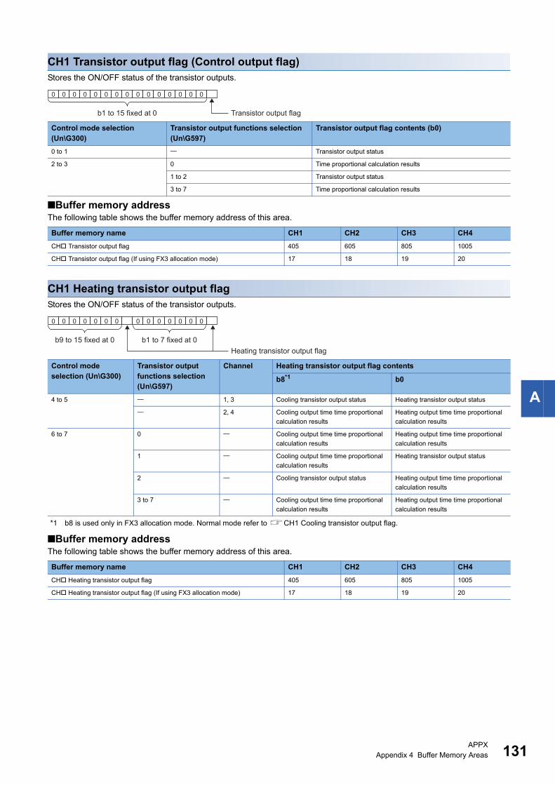
A
CH1 Transistor output flag (Control output flag)Stores the ON/OFF status of the transistor outputs.
■Buffer memory addressThe following table shows the buffer memory address of this area.
CH1 Heating transistor output flagStores the ON/OFF status of the transistor outputs.
*1 b8 is used only in FX3 allocation mode. Normal mode refer to CH1 Cooling transistor output flag.
■Buffer memory addressThe following table shows the buffer memory address of this area.
Control mode selection (Un\G300)
Transistor output functions selection (Un\G597)
Transistor output flag contents (b0)
0 to 1 Transistor output status
2 to 3 0 Time proportional calculation results
1 to 2 Transistor output status
3 to 7 Time proportional calculation results
Buffer memory name CH1 CH2 CH3 CH4
CH Transistor output flag 405 605 805 1005
CH Transistor output flag (If using FX3 allocation mode) 17 18 19 20
Control mode selection (Un\G300)
Transistor output functions selection (Un\G597)
Channel Heating transistor output flag contents
b8*1 b0
4 to 5 1, 3 Cooling transistor output status Heating transistor output status
2, 4 Cooling output time time proportional
calculation results
Heating output time time proportional
calculation results
6 to 7 0 Cooling output time time proportional
calculation results
Heating output time time proportional
calculation results
1 Cooling output time time proportional
calculation results
Heating transistor output status
2 Cooling transistor output status Heating output time time proportional
calculation results
3 to 7 Cooling output time time proportional
calculation results
Heating output time time proportional
calculation results
Buffer memory name CH1 CH2 CH3 CH4
CH Heating transistor output flag 405 605 805 1005
CH Heating transistor output flag (If using FX3 allocation mode) 17 18 19 20
Transistor output flag
0 0 0 0 0 0 0 00 0 0 0 0 0 0
b1 to 15 fixed at 0
Heating transistor output flag
0 0 0 0 0 0 0 0 0 0 0 0 0 0
b9 to 15 fixed at 0 b1 to 7 fixed at 0
APPXAppendix 4 Buffer Memory Areas 131
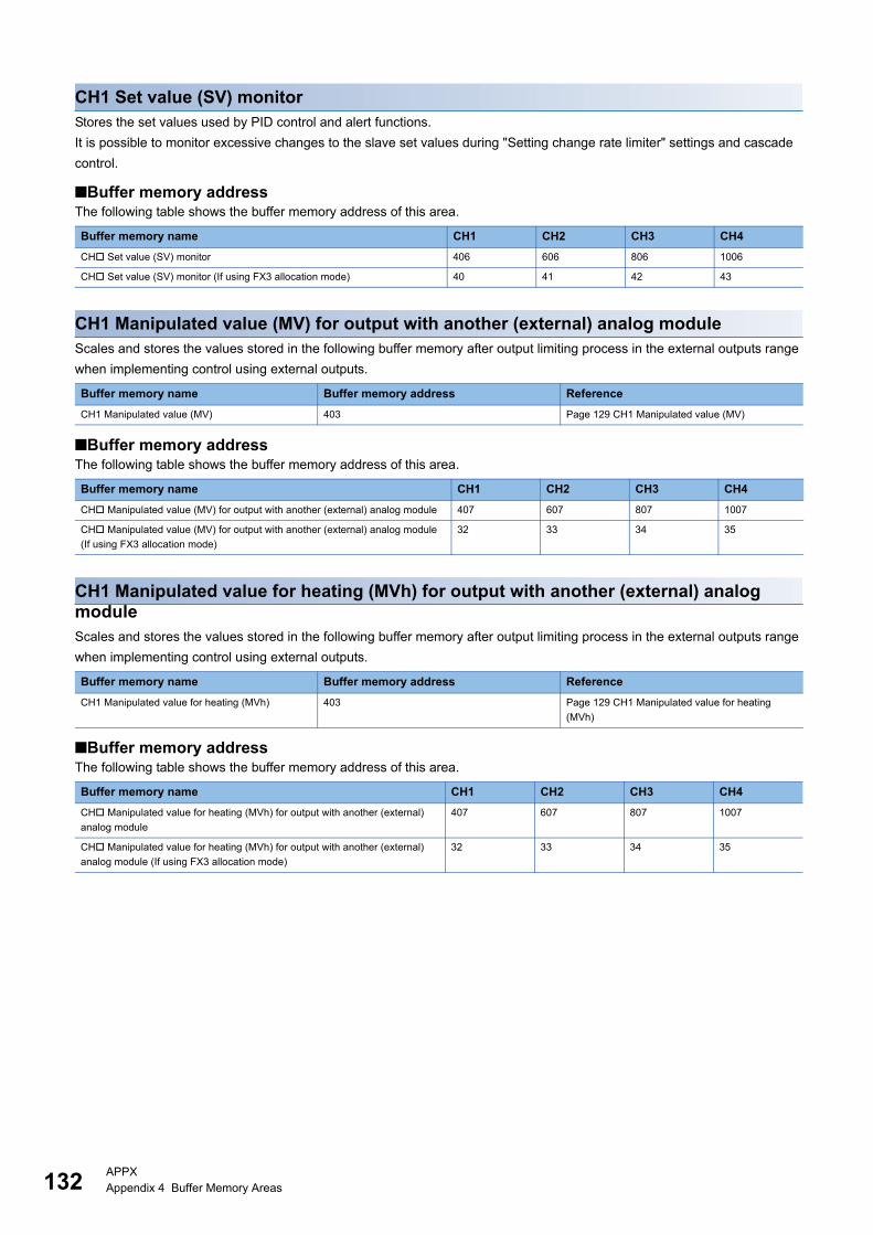
13
CH1 Set value (SV) monitorStores the set values used by PID control and alert functions.
It is possible to monitor excessive changes to the slave set values during "Setting change rate limiter" settings and cascade
control.
■Buffer memory addressThe following table shows the buffer memory address of this area.
CH1 Manipulated value (MV) for output with another (external) analog moduleScales and stores the values stored in the following buffer memory after output limiting process in the external outputs range
when implementing control using external outputs.
■Buffer memory addressThe following table shows the buffer memory address of this area.
CH1 Manipulated value for heating (MVh) for output with another (external) analog moduleScales and stores the values stored in the following buffer memory after output limiting process in the external outputs range
when implementing control using external outputs.
■Buffer memory addressThe following table shows the buffer memory address of this area.
Buffer memory name CH1 CH2 CH3 CH4
CH Set value (SV) monitor 406 606 806 1006
CH Set value (SV) monitor (If using FX3 allocation mode) 40 41 42 43
Buffer memory name Buffer memory address Reference
CH1 Manipulated value (MV) 403 Page 129 CH1 Manipulated value (MV)
Buffer memory name CH1 CH2 CH3 CH4
CH Manipulated value (MV) for output with another (external) analog module 407 607 807 1007
CH Manipulated value (MV) for output with another (external) analog module
(If using FX3 allocation mode)
32 33 34 35
Buffer memory name Buffer memory address Reference
CH1 Manipulated value for heating (MVh) 403 Page 129 CH1 Manipulated value for heating
(MVh)
Buffer memory name CH1 CH2 CH3 CH4
CH Manipulated value for heating (MVh) for output with another (external)
analog module
407 607 807 1007
CH Manipulated value for heating (MVh) for output with another (external)
analog module (If using FX3 allocation mode)
32 33 34 35
2APPXAppendix 4 Buffer Memory Areas
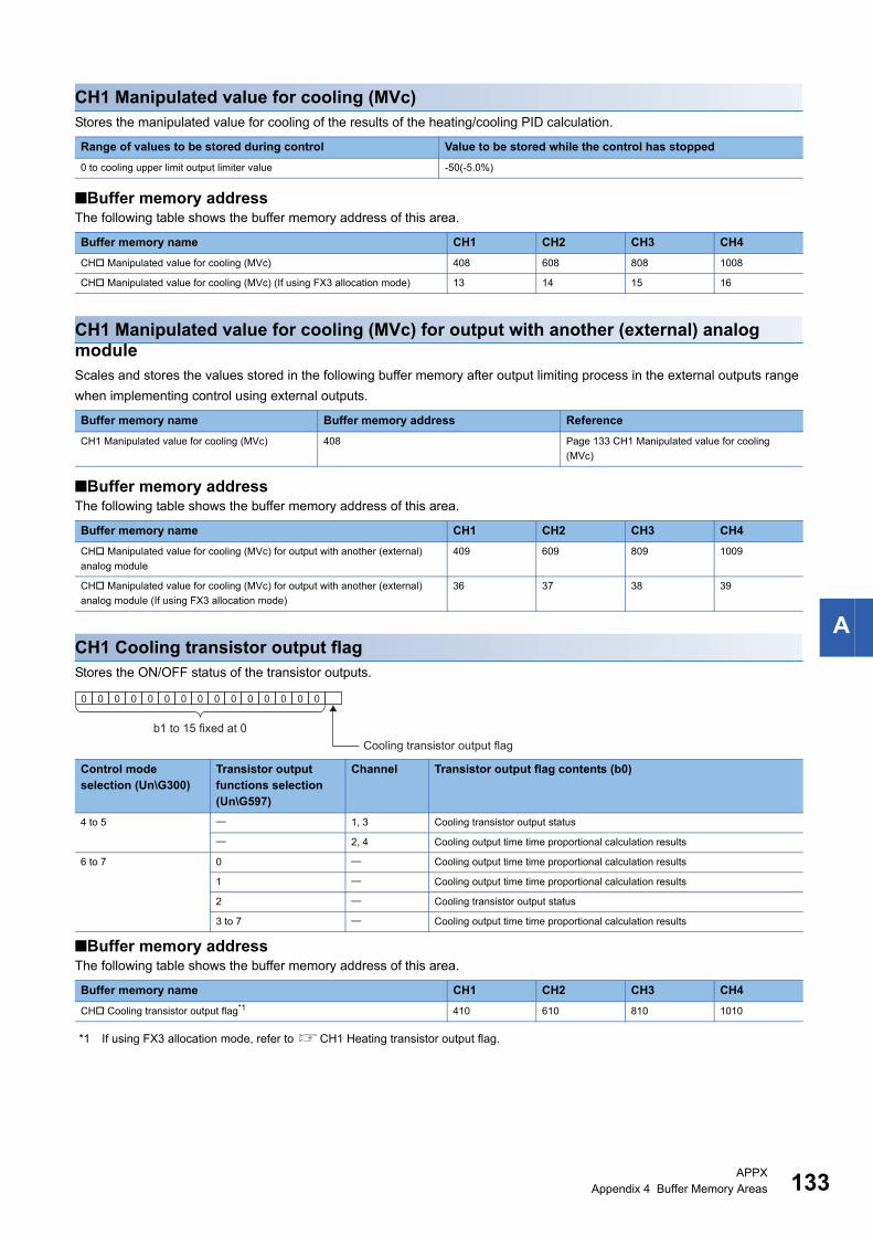
A
CH1 Manipulated value for cooling (MVc)Stores the manipulated value for cooling of the results of the heating/cooling PID calculation.
■Buffer memory addressThe following table shows the buffer memory address of this area.
CH1 Manipulated value for cooling (MVc) for output with another (external) analog moduleScales and stores the values stored in the following buffer memory after output limiting process in the external outputs range
when implementing control using external outputs.
■Buffer memory addressThe following table shows the buffer memory address of this area.
CH1 Cooling transistor output flagStores the ON/OFF status of the transistor outputs.
■Buffer memory addressThe following table shows the buffer memory address of this area.
*1 If using FX3 allocation mode, refer to CH1 Heating transistor output flag.
Range of values to be stored during control Value to be stored while the control has stopped
0 to cooling upper limit output limiter value -50(-5.0%)
Buffer memory name CH1 CH2 CH3 CH4
CH Manipulated value for cooling (MVc) 408 608 808 1008
CH Manipulated value for cooling (MVc) (If using FX3 allocation mode) 13 14 15 16
Buffer memory name Buffer memory address Reference
CH1 Manipulated value for cooling (MVc) 408 Page 133 CH1 Manipulated value for cooling
(MVc)
Buffer memory name CH1 CH2 CH3 CH4
CH Manipulated value for cooling (MVc) for output with another (external)
analog module
409 609 809 1009
CH Manipulated value for cooling (MVc) for output with another (external)
analog module (If using FX3 allocation mode)
36 37 38 39
Control mode selection (Un\G300)
Transistor output functions selection (Un\G597)
Channel Transistor output flag contents (b0)
4 to 5 1, 3 Cooling transistor output status
2, 4 Cooling output time time proportional calculation results
6 to 7 0 Cooling output time time proportional calculation results
1 Cooling output time time proportional calculation results
2 Cooling transistor output status
3 to 7 Cooling output time time proportional calculation results
Buffer memory name CH1 CH2 CH3 CH4
CH Cooling transistor output flag*1 410 610 810 1010
Cooling transistor output flag
0 0 0 0 0 0 0 0 0 0 0 0 0 0 0
b1 to 15 fixed at 0
APPXAppendix 4 Buffer Memory Areas 133
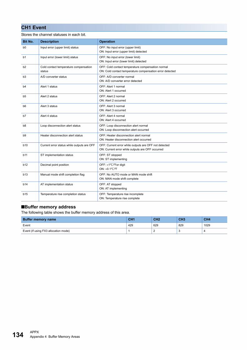
13
CH1 EventStores the channel statuses in each bit.
■Buffer memory addressThe following table shows the buffer memory address of this area.
Bit No. Description Operation
b0 Input error (upper limit) status OFF: No input error (upper limit)
ON: Input error (upper limit) detected
b1 Input error (lower limit) status OFF: No input error (lower limit)
ON: Input error (lower limit) detected
b2 Cold contact temperature compensation
status
OFF: Cold contact temperature compensation normal
ON: Cold contact temperature compensation error detected
b3 A/D converter status OFF: A/D converter normal
ON: A/D converter error detected
b4 Alert 1 status OFF: Alert 1 normal
ON: Alert 1 occurred
b5 Alert 2 status OFF: Alert 2 normal
ON: Alert 2 occurred
b6 Alert 3 status OFF: Alert 3 normal
ON: Alert 3 occurred
b7 Alert 4 status OFF: Alert 4 normal
ON: Alert 4 occurred
b8 Loop disconnection alert status OFF: Loop disconnection alert normal
ON: Loop disconnection alert occurred
b9 Heater disconnection alert status OFF: Heater disconnection alert normal
ON: Heater disconnection alert occurred
b10 Current error status while outputs are OFF OFF: Current error while outputs are OFF not detected
ON: Current error while outputs are OFF occurred
b11 ST implementation status OFF: ST stopped
ON: ST implementing
b12 Decimal point position OFF: ×1/or digit
ON: ×0.1/
b13 Manual mode shift completion flag OFF: No AUTO mode or MAN mode shift
ON: MAN mode shift complete
b14 AT implementation status OFF: AT stopped
ON: AT implementing
b15 Temperature rise completion status OFF: Temperature rise incomplete
ON: Temperature rise complete
Buffer memory name CH1 CH2 CH3 CH4
Event 429 629 829 1029
Event (If using FX3 allocation mode) 1 2 3 4
4APPXAppendix 4 Buffer Memory Areas
A
CH1 Set value (SV) settingSets the PID control and alert process set values.
■Buffer memory addressThe following table shows the buffer memory address of this area.
■Setting rangeThe range is determined by the values set in 'CH1 Upper limit setting limiter' (Un\G511) and 'CH1 Lower limit setting limiter'
(Un\G512). (Page 147 CH1 Upper limit setting limiter, Page 147 CH1 Lower limit setting limiter)
When a value out of the setting range is set in this area, an out of setting range error (error code: 1950H) occurs, and the
status is as described below.
• 'Error flag' (Un\G398, b2) turns ON.
• An error code is stored in 'Latest error code' (Un\G0).
■Setting unitThe value to be set differs depending on the value stored in 'CH1 Decimal point position' (Un\G400). (Page 128 CH1
Decimal point position)
• No decimal point (0): Set a value in increments of 1 ( or digit).
• If there is 1 digit (1) past the decimal point: Set a value (the value multiplied by 10) in increments of 0.1 ().
■Default valueThe default value is 0.
CH1 Proportional band (P) settingSet the proportional band (P) to execute the standard PID control.
■Buffer memory addressThe following table shows the buffer memory address of this area.
■Setting range0 to 10000 (span*1 0.0 to 1000.0%)
*1 During internal temperature inputs, input range span. During internal micro voltage inputs, scaling span. During external inputs, external input span.
■Two-position controlSet the proportional band (P) to 0.
For details on the two-position control, refer to the following.
Page 26 Control Method
■Default valueThe default value is 30 (3.0%).
Buffer memory name CH1 CH2 CH3 CH4
CH Set value (SV) setting 430 630 830 1030
CH Set value (SV) setting (If using FX3 allocation mode) 48 88 128 168
Buffer memory name CH1 CH2 CH3 CH4
CH Proportional band (P) setting 431 631 831 1031
CH Proportional band (P) setting (If using FX3 allocation mode) 58 98 138 178
APPXAppendix 4 Buffer Memory Areas 135
13
CH1 Heating proportional band (Ph) settingSet the heating proportional band (Ph) to implement the heating and cooling PID control.
■Buffer memory addressThe following table shows the buffer memory address of this area.
■Setting range0 to 10000 (span*1 0.0 to 1000.0%)
*1 During internal temperature inputs, input range span. During internal micro voltage inputs, scaling span. During external inputs, external input span.
■Two-position controlSet the heating proportional band (Ph) to 0.
For details on the two-position control, refer to the following.
Page 26 Control Method
■Default valueThe default value is 30 (3.0%).
CH1 Integral time (I) settingSet the integral time (I) to execute the PID control.
■Buffer memory addressThe following table shows the buffer memory address of this area.
■Setting rangeThe setting range is 0 to 3600 (0 to 3600s).
■P control or PD controlSet 0. For details on control methods, refer to the following.
Page 26 Control Method
■Default valueThe default value is 240 (240s).
Buffer memory name CH1 CH2 CH3 CH4
CH Heating proportional band (Ph) setting 431 631 831 1031
CH Heating proportional band (Ph) setting (If using FX3 allocation mode) 58 98 138 178
Buffer memory name CH1 CH2 CH3 CH4
CH Integral time (I) setting 432 632 832 1032
CH Integral time (I) setting (If using FX3 allocation mode) 60 100 140 180
6APPXAppendix 4 Buffer Memory Areas
A
CH1 Derivative time (D) settingSet the derivative time (D) to execute the PID control.
■Buffer memory addressThe following table shows the buffer memory address of this area.
■Setting rangeThe setting range is 0 to 3600 (0 to 3600s).
■P control or PI controlSet 0. For details on control methods, refer to the following.
Page 26 Control Method
■Default valueThe default value is 60 (60s).
CH1 Alert set value 1Set the temperature to turn ON CH1 alert 1 (Un\G401, b8) according to the selected alert 1 'alert mode' (Un\G533).
For 'CH1 Warning Occurrence Contents' (Un\G401), refer to the following.
Page 128 CH1 Alert definition
For details of the alert function, refer to the following.
Page 54 Alert Function
■Buffer memory addressThe following table shows the buffer memory address of this area.
■Alert modeSet the alert mode of Alert 1 in the following buffer memory area. The alert mode of Alert 1 corresponds to 'CH1 Alert set
value 1' (Un\G434).
• 'CH1 Alert 1 mode setting' (Un\G533)
■Setting rangeThe write set value units and settings range depend on the alert mode that has been set.
*1 During internal temperature inputs, input range. During internal micro voltage inputs, scaling range. During external inputs, external input range.
*2 During internal temperature inputs, input range span. During internal micro voltage inputs, scaling span. During external inputs, external input span.
Buffer memory name CH1 CH2 CH3 CH4
CH Differential time (D) setting 433 633 833 1033
CH Differential time (D) setting (If using FX3 allocation mode) 61 101 141 181
Buffer memory name CH1 CH2 CH3 CH4
CH Alert set value 1 434 634 834 1034
CH Alert set value 1 (If using FX3 allocation mode) 49 89 129 169
Alert mode Setting range of alert set value Remarks
No alert 0
Upper limit input alert, lower limit input alert Same as the input range.*1 Same as with wait.
Upper limit deviation alert, lower limit deviation
alert
- span to + span*2 Same as with wait and re-wait.
Upper/lower limit deviation alert, within range alert 0 to + span*2 Same as with wait and re-wait.
APPXAppendix 4 Buffer Memory Areas 137
13
■Setting unitThe value to be set differs depending on the value stored in 'CH1 Decimal point position' (Un\G400). (Page 128 CH1
Decimal point position)
• No decimal point (0): Set a value in increments of 1 ( or digit).
• If there is 1 digit (1) past the decimal point: Set a value (the value multiplied by 10) in increments of 0.1 ().
■Default valueThe default value is 0.
CH1 Alert set value 2Set the temperature to turn ON CH1 alert 2 (Un\G401, b9) according to the selected alert 2 'alert mode' (Un\G533).
For 'CH1 Warning Occurrence Contents' (Un\G401), refer to the following.
Page 128 CH1 Alert definition
For details of the alert function, refer to the following.
Page 54 Alert Function
■Buffer memory addressThe following table shows the buffer memory address of this area.
■Alert modeSet the alert mode of Alert 2 in the following buffer memory area. The alert mode of Alert 2 corresponds to 'CH1 Alert set
value 2' (Un\G435).
• 'CH1 Alert 2 mode setting' (Un\G534)
■Setting rangeFor the settings range, refer to the following.
Page 137 Setting range
■Setting unitFor the settings unit, refer to the following.
Page 138 Setting unit
■Default valueThe default value is 0.
Buffer memory name CH1 CH2 CH3 CH4
CH Alert set value 2 435 635 835 1035
CH Alert set value 2 (If using FX3 allocation mode) 50 90 130 170
8APPXAppendix 4 Buffer Memory Areas
A
CH1 Alert set value 3Set the temperature to turn ON CH1 alert 3 (Un\G401, b10) according to the selected alert 3 'alert mode' (Un\G533).
For 'CH1 Warning Occurrence Contents' (Un\G401), refer to the following.
Page 128 CH1 Alert definition
For details of the alert function, refer to the following.
Page 54 Alert Function
■Buffer memory addressThe following table shows the buffer memory address of this area.
■Alert modeSet the alert mode of Alert 3 in the following buffer memory area. The alert mode of Alert 3 corresponds to 'CH1 Alert set
value 3' (Un\G436).
• 'CH1 Alert 3 mode setting' (Un\G535)
■Setting rangeFor the settings range, refer to the following.
Page 137 Setting range
■Setting unitFor the settings unit, refer to the following.
Page 138 Setting unit
■Default valueThe default value is 0.
CH1 Alert set value 4Set the temperature to turn ON CH1 alert 4 (Un\G401, b11) according to the selected alert 4 'alert mode' (Un\G533).
For 'CH1 Warning Occurrence Contents' (Un\G401), refer to the following.
Page 128 CH1 Alert definition
For details of the alert function, refer to the following.
Page 54 Alert Function
■Buffer memory addressThe following table shows the buffer memory address of this area.
■Alert modeSet the alert mode of Alert 4 in the following buffer memory area. The alert mode of alert 4 corresponds to 'CH1 alert set value
4' (Un\G437).
• 'CH1 Alert 4 mode setting' (Un\G536)
■Setting rangeFor the settings range, refer to the following.
Page 137 Setting range
■Setting unitFor the setting unit, refer to the following.
Page 138 Setting unit
■Default valueThe default value is 0.
Buffer memory name CH1 CH2 CH3 CH4
CH Alert set value 3 436 636 836 1036
CH Alert set value 3 (If using FX3 allocation mode) 51 91 131 171
Buffer memory name CH1 CH2 CH3 CH4
CH Alert set value 4 437 637 837 1037
CH Alert set value 4 (If using FX3 allocation mode) 52 92 132 172
APPXAppendix 4 Buffer Memory Areas 139
14
CH1 Temperature process value (PV) for input with another (external) analog moduleThe digital input value of the current or voltage converted in another analog module on the system can be used as a
temperature process value (PV). Store the digital input value of the current or voltage converted by another analog module in
this area. For details, refer to the following.
Page 50 Input
Precautions
• If a greater value than (external input range upper limit +5% of external input range) is set, an input upper limit alert occurs,
and 'CH1 event' (Un\G429) b0 turns ON.
• If a smaller value than (external input range lower limit -5% of external input range) is set, an input lower limit alert occurs,
and 'CH1 event' (Un\G429) b1 turns ON.
■Buffer memory addressThe following table shows the buffer memory address of this area.
■Default valueThe default value is 0.
CH1 Cooling proportional band (Pc) settingSet the cooling proportional band (Pc) to implement the heating and cooling PID control.
■Buffer memory addressThe following table shows the buffer memory address of this area.
■Setting range1 to 10000 (span*1 0.1 to 1000.0%)
*1 During internal temperature inputs, input range span. During internal micro voltage inputs, scaling span. During external inputs, external input span.
■Default valueThe default value is 30 (3.0%).
CH1 Input rangeSelect the input type used by the temperature control module.
■Buffer memory addressThe following table shows the buffer memory address of this area.
Buffer memory name CH1 CH2 CH3 CH4
CH Temperature process value (PV) for input with another (external) analog
module
438 638 838 1038
CH Temperature process value (PV) for input with another (external) analog
module (If using FX3 allocation mode)
25 26 27 28
Buffer memory name CH1 CH2 CH3 CH4
CH Cooling proportional band (Pc) setting 439 639 839 1039
CH Cooling proportional band (Pc) setting (If using FX3 allocation mode) 59 99 139 179
Buffer memory name CH1 CH2 CH3 CH4
CH Input range 501 701 901 1101
CH input range (If using FX3 allocation mode) 208 214 220 226
0APPXAppendix 4 Buffer Memory Areas
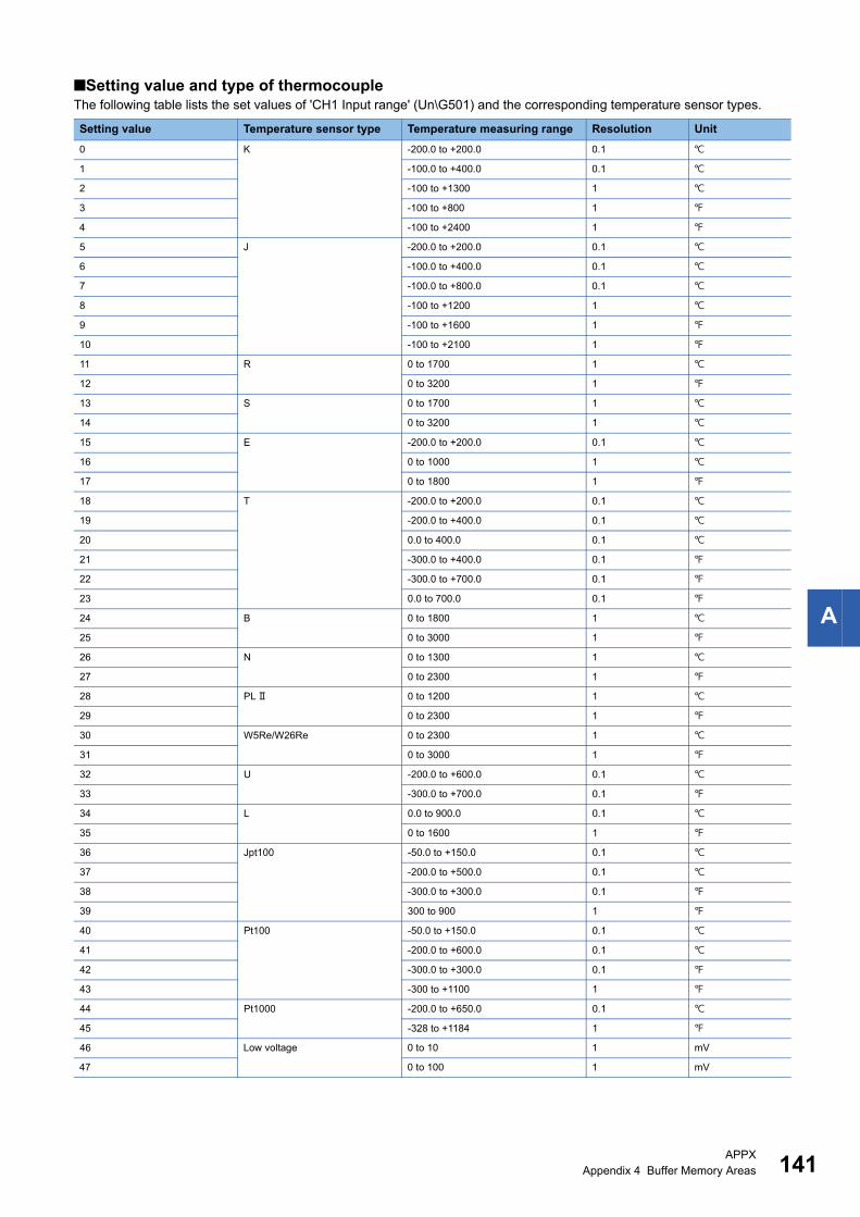
A
■Setting value and type of thermocoupleThe following table lists the set values of 'CH1 Input range' (Un\G501) and the corresponding temperature sensor types.
Setting value Temperature sensor type Temperature measuring range Resolution Unit
0 K -200.0 to +200.0 0.1
1 -100.0 to +400.0 0.1
2 -100 to +1300 1
3 -100 to +800 1
4 -100 to +2400 1
5 J -200.0 to +200.0 0.1
6 -100.0 to +400.0 0.1
7 -100.0 to +800.0 0.1
8 -100 to +1200 1
9 -100 to +1600 1
10 -100 to +2100 1
11 R 0 to 1700 1
12 0 to 3200 1
13 S 0 to 1700 1
14 0 to 3200 1
15 E -200.0 to +200.0 0.1
16 0 to 1000 1
17 0 to 1800 1
18 T -200.0 to +200.0 0.1
19 -200.0 to +400.0 0.1
20 0.0 to 400.0 0.1
21 -300.0 to +400.0 0.1
22 -300.0 to +700.0 0.1
23 0.0 to 700.0 0.1
24 B 0 to 1800 1
25 0 to 3000 1
26 N 0 to 1300 1
27 0 to 2300 1
28 PL 0 to 1200 1
29 0 to 2300 1
30 W5Re/W26Re 0 to 2300 1
31 0 to 3000 1
32 U -200.0 to +600.0 0.1
33 -300.0 to +700.0 0.1
34 L 0.0 to 900.0 0.1
35 0 to 1600 1
36 Jpt100 -50.0 to +150.0 0.1
37 -200.0 to +500.0 0.1
38 -300.0 to +300.0 0.1
39 300 to 900 1
40 Pt100 -50.0 to +150.0 0.1
41 -200.0 to +600.0 0.1
42 -300.0 to +300.0 0.1
43 -300 to +1100 1
44 Pt1000 -200.0 to +650.0 0.1
45 -328 to +1184 1
46 Low voltage 0 to 10 1 mV
47 0 to 100 1 mV
APPXAppendix 4 Buffer Memory Areas 141
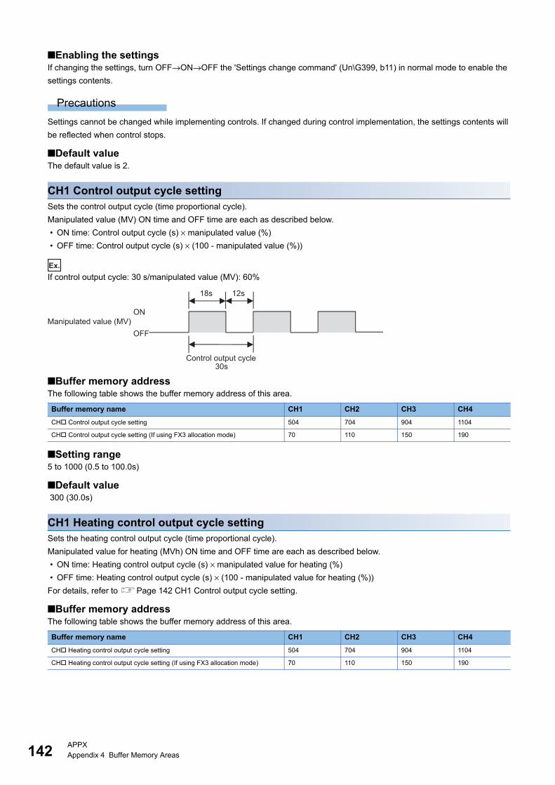
14
■Enabling the settingsIf changing the settings, turn OFF→ON→OFF the 'Settings change command' (Un\G399, b11) in normal mode to enable the
settings contents.
Precautions
Settings cannot be changed while implementing controls. If changed during control implementation, the settings contents will
be reflected when control stops.
■Default valueThe default value is 2.
CH1 Control output cycle settingSets the control output cycle (time proportional cycle).
Manipulated value (MV) ON time and OFF time are each as described below.
• ON time: Control output cycle (s) × manipulated value (%)
• OFF time: Control output cycle (s) × (100 - manipulated value (%))
Ex.
If control output cycle: 30 s/manipulated value (MV): 60%
■Buffer memory addressThe following table shows the buffer memory address of this area.
■Setting range5 to 1000 (0.5 to 100.0s)
■Default value 300 (30.0s)
CH1 Heating control output cycle settingSets the heating control output cycle (time proportional cycle).
Manipulated value for heating (MVh) ON time and OFF time are each as described below.
• ON time: Heating control output cycle (s) × manipulated value for heating (%)
• OFF time: Heating control output cycle (s) × (100 - manipulated value for heating (%))
For details, refer to Page 142 CH1 Control output cycle setting.
■Buffer memory addressThe following table shows the buffer memory address of this area.
Buffer memory name CH1 CH2 CH3 CH4
CH Control output cycle setting 504 704 904 1104
CH Control output cycle setting (If using FX3 allocation mode) 70 110 150 190
Buffer memory name CH1 CH2 CH3 CH4
CH Heating control output cycle setting 504 704 904 1104
CH Heating control output cycle setting (If using FX3 allocation mode) 70 110 150 190
Manipulated value (MV)ON
OFF
Control output cycle30s
18s 12s
2APPXAppendix 4 Buffer Memory Areas
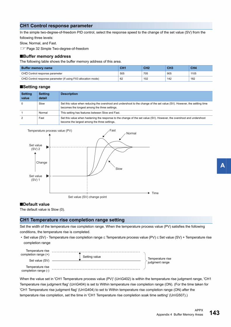
A
CH1 Control response parameterIn the simple two-degree-of-freedom PID control, select the response speed to the change of the set value (SV) from the
following three levels:
Slow, Normal, and Fast.
Page 32 Simple Two-degree-of-freedom
■Buffer memory addressThe following table shows the buffer memory address of this area.
■Setting range
■Default valueThe default value is Slow (0).
CH1 Temperature rise completion range settingSet the width of the temperature rise completion range. When the temperature process value (PV) satisfies the following
conditions, the temperature rise is completed.
• Set value (SV) - Temperature rise completion range ≤ Temperature process value (PV) ≤ Set value (SV) + Temperature rise
completion range
When the value set in 'CH1 Temperature process value (PV)' (Un\G402) is within the temperature rise judgment range, 'CH1
Temperature rise judgment flag' (Un\G404) is set to Within temperature rise completion range (ON). (For the time taken for
'CH1 Temperature rise judgment flag' (Un\G404) to set to Within temperature rise completion range (ON) after the
temperature rise completion, set the time in 'CH1 Temperature rise completion soak time setting' (Un\G507).)
Buffer memory name CH1 CH2 CH3 CH4
CH Control response parameter 505 705 905 1105
CH Control response parameter (If using FX3 allocation mode) 62 102 142 182
Setting value
Setting detail
Description
0 Slow Set this value when reducing the overshoot and undershoot to the change of the set value (SV). However, the settling time
becomes the longest among the three settings.
1 Normal This setting has features between Slow and Fast.
2 Fast Set this value when hastening the response to the change of the set value (SV). However, the overshoot and undershoot
become the largest among the three settings.
Time
Temperature process value (PV)
Set value(SV) 2
Set value(SV) 1
Change
Set value (SV) change point
FastNormal
Slow
Temperature risecompletion range (+)
Set value (SV)
Temperature rise completion range (-)
Temperature rise judgment range
Setting value
APPXAppendix 4 Buffer Memory Areas 143
14
■Buffer memory addressThe following table shows the buffer memory address of this area.
■Setting range1 to 100 (/ or digit)
■Default valueThe default value is 10.
CH1 Temperature rise completion soak time settingSet the time taken to set 'CH1 Temperature rise judgment flag' (Un\G404) to Within temperature rise completion range (ON)
after the completion of the temperature rise.
■Buffer memory addressThe following table shows the buffer memory address of this area.
■Setting rangeThe setting range is 0 to 3600 (min).
■Default valueThe default value is 0 (min).
CH1 Upper limit output limiterSet the upper limit value for actually outputting the manipulated value (MV) calculated by the standard PID operation to an
external device.
■Buffer memory addressThe following table shows the buffer memory address of this area.
■Setting rangeThe lower limit output limiter +1 to 1050 (105.0% max.).
Set values so that the lower limit output limiter value is smaller than the upper limit output limiter value.
When the lower limit output limiter value is equal to or greater than the upper limit output limiter value, CH Upper/lower limit
output limiter setting error (error code: 1A0H) occurs.
When a value out of the setting value is set, an out of setting range error (error code: 1950H) occurs. When an error has
occurred, the following operations will be executed.
• 'Error flag' (Un\G398, b2) turns ON.
• An error code is stored in 'Latest error code' (Un\G0).
■Two-position controlIn the two-position control, this setting is disabled.
■Default valueThe default value is 1000 (100.0%).
Buffer memory name CH1 CH2 CH3 CH4
CH Temperature rise completion range setting 506 706 906 1106
Temperature rise completion range setting (If using FX3 allocation mode) 236
Buffer memory name CH1 CH2 CH3 CH4
CH Temperature rise completion soak time setting 507 707 907 1107
Temperature rise completion soak time setting (If using FX3 allocation mode) 237
Buffer memory name CH1 CH2 CH3 CH4
CH Upper limit output limiter 508 708 908 1108
CH Upper limit output limiter (If using FX3 allocation mode) 64 104 144 184
4APPXAppendix 4 Buffer Memory Areas
A
CH1 Heating upper limit output limiterSet the upper limit value for actually outputting the manipulated value for heating (MVh) calculated by the heating and cooling
PID operation to an external device. In the auto tuning, this setting is ignored.
■Buffer memory addressThe following table shows the buffer memory address of this area.
■Setting rangeThis is 0 to 1050 (0.0 to 105.0%).
When a value out of the setting value is set, an out of setting range error (error code: 1950H) occurs. When an error has
occurred, the following operations will be executed.
• 'Error flag' (Un\G398, b2) turns ON.
• An error code is stored in 'Latest error code' (Un\G0).
In the heating-cooling PID control, the lower limit value is not used. When 'CH1 Lower limit output limiter'
(Un\G509) is set to a value other than 0, an out of setting range error (error code: 1950H) occurs.
■Two-position controlIn the two-position control, this setting is disabled.
■Default valueThe default value is 1000 (100.0%).
CH1 Lower limit output limiterSet the lower limit value for actually outputting the manipulated value (MV) calculated by the PID operation to an external
device.
■Buffer memory addressThe following table shows the buffer memory address of this area.
■Setting range-50 to upper limit output limiter -1 (-5.0% min.)
Set values so that the lower limit output limiter value is smaller than the upper limit output limiter value.
When the lower limit output limiter value is equal to or greater than the upper limit output limiter value, CH Upper/lower limit
output limiter setting error (error code: 1A0H) occurs.
When a value out of the setting value is set, an out of setting range error (error code: 1950H) occurs. When an error has
occurred, the following operations will be executed.
• 'Error flag' (Un\G398, b2) turns ON.
• An error code is stored in 'Latest error code' (Un\G0).
■Two-position controlIn the two-position control, this setting is disabled.
■Default valueThe default value is 0 (0.0%).
Buffer memory name CH1 CH2 CH3 CH4
CH Heating upper limit output limiter 508 708 908 1108
CH Heating upper limit output limiter (If using FX3 allocation mode) 42 74 106 138
Buffer memory name CH1 CH2 CH3 CH4
CH Lower limit output limiter 509 709 909 1109
CH Lower limit output limiter (If using FX3 allocation mode) 65 105 145 185
APPXAppendix 4 Buffer Memory Areas 145
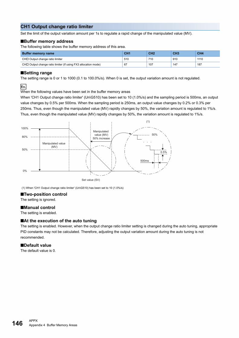
14
CH1 Output change ratio limiterSet the limit of the output variation amount per 1s to regulate a rapid change of the manipulated value (MV).
■Buffer memory addressThe following table shows the buffer memory address of this area.
■Setting rangeThe setting range is 0 or 1 to 1000 (0.1 to 100.0%/s). When 0 is set, the output variation amount is not regulated.
Ex.
When the following values have been set in the buffer memory areas
When 'CH1 Output change ratio limiter' (Un\G510) has been set to 10 (1.0%/s) and the sampling period is 500ms, an output
value changes by 0.5% per 500ms. When the sampling period is 250ms, an output value changes by 0.2% or 0.3% per
250ms. Thus, even though the manipulated value (MV) rapidly changes by 50%, the variation amount is regulated to 1%/s.
Thus, even though the manipulated value (MV) rapidly changes by 50%, the variation amount is regulated to 1%/s.
■Two-position controlThe setting is ignored.
■Manual controlThe setting is enabled.
■At the execution of the auto tuningThe setting is enabled. However, when the output change ratio limiter setting is changed during the auto tuning, appropriate
PID constants may not be calculated. Therefore, adjusting the output variation amount during the auto tuning is not
recommended.
■Default valueThe default value is 0.
Buffer memory name CH1 CH2 CH3 CH4
CH Output change ratio limiter 510 710 910 1110
CH Output change ratio limiter (If using FX3 allocation mode) 67 107 147 187
(1) When 'CH1 Output change ratio limiter' (Un\G510) has been set to 10 (1.0%/s)
(1)
100%
50%
0%
80%
500ms
0.5%
50%
Set value (SV)
50% increase
Manipulated value (MV)
Manipulated value (MV)
6APPXAppendix 4 Buffer Memory Areas
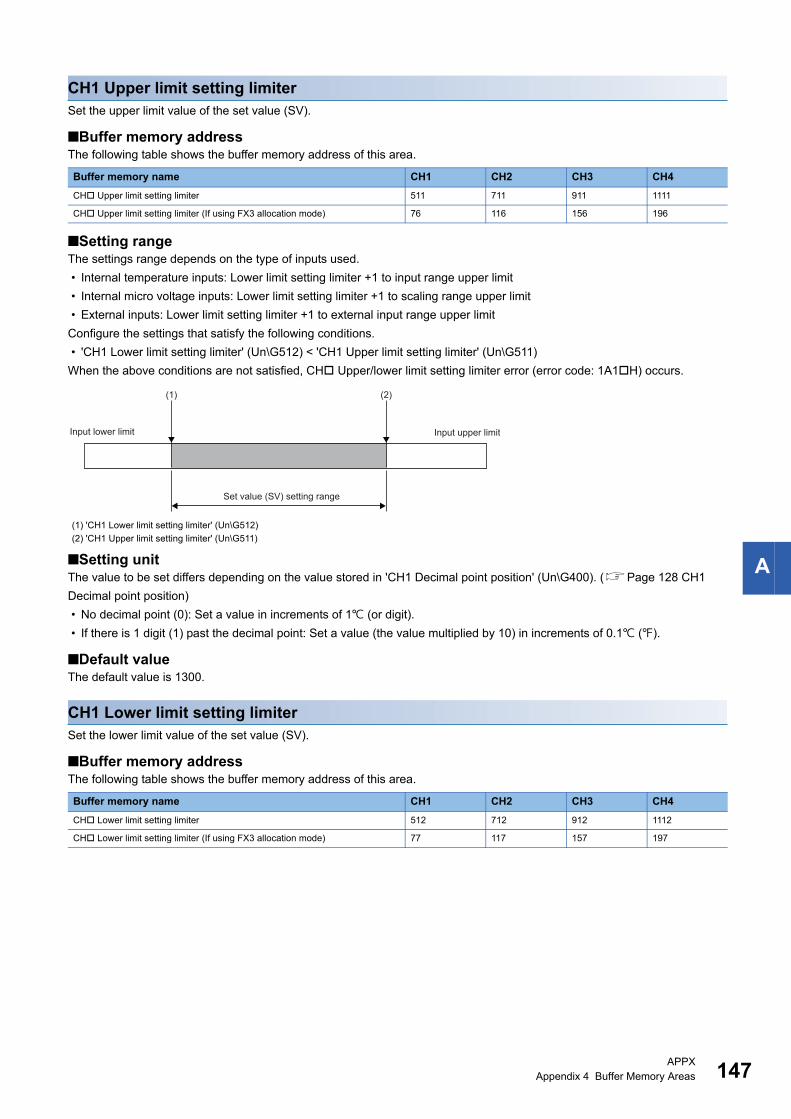
A
CH1 Upper limit setting limiterSet the upper limit value of the set value (SV).
■Buffer memory addressThe following table shows the buffer memory address of this area.
■Setting rangeThe settings range depends on the type of inputs used.
• Internal temperature inputs: Lower limit setting limiter +1 to input range upper limit
• Internal micro voltage inputs: Lower limit setting limiter +1 to scaling range upper limit
• External inputs: Lower limit setting limiter +1 to external input range upper limit
Configure the settings that satisfy the following conditions.
• 'CH1 Lower limit setting limiter' (Un\G512) < 'CH1 Upper limit setting limiter' (Un\G511)
When the above conditions are not satisfied, CH Upper/lower limit setting limiter error (error code: 1A1H) occurs.
■Setting unitThe value to be set differs depending on the value stored in 'CH1 Decimal point position' (Un\G400). (Page 128 CH1
Decimal point position)
• No decimal point (0): Set a value in increments of 1 (or digit).
• If there is 1 digit (1) past the decimal point: Set a value (the value multiplied by 10) in increments of 0.1 ().
■Default valueThe default value is 1300.
CH1 Lower limit setting limiterSet the lower limit value of the set value (SV).
■Buffer memory addressThe following table shows the buffer memory address of this area.
Buffer memory name CH1 CH2 CH3 CH4
CH Upper limit setting limiter 511 711 911 1111
CH Upper limit setting limiter (If using FX3 allocation mode) 76 116 156 196
(1) 'CH1 Lower limit setting limiter' (Un\G512)
(2) 'CH1 Upper limit setting limiter' (Un\G511)
Buffer memory name CH1 CH2 CH3 CH4
CH Lower limit setting limiter 512 712 912 1112
CH Lower limit setting limiter (If using FX3 allocation mode) 77 117 157 197
(1) (2)
Input upper limit
Set value (SV) setting range
Input lower limit
APPXAppendix 4 Buffer Memory Areas 147
14
■Setting rangeThe settings range depends on the type of inputs used.
• Internal temperature inputs: Input range lower limit to upper limit setting limiter -1
• Internal low voltage: Scaling range lower limit to upper limit setting limiter -1
• External inputs: External input range lower limit to upper limit setting limiter -1
■Setting unitFor the setting unit, refer to the following.
Page 147 Setting unit
■Default valueThe default value is -100.
CH1 Setting change rate limiterSets the set value (SV) change rate per minute when changing the set value (SV). This setting can regulate a rapid change of
the manipulated value (MV).
■Buffer memory addressThe following table shows the buffer memory address of this area.
■Setting range0 to 1000 (span*1 0.1 to 100.0%). When 0 is set, this setting is disabled.
*1 During internal temperature inputs, input range span. During internal micro voltage inputs, scaling span. During external inputs, external input span.
■Default valueSet to disabled (0).
CH1 Normal/Reverse operation settingSelect whether to use CH1 with normal operations or reverse operations.
Select normal operations for the cooling control. Select reverse operations for the heating control.
For details on the normal/reverse operation selection function, refer to the following.
Page 32 Normal/Reverse Operation Selection Function
■Buffer memory addressThe following table shows the buffer memory address of this area.
■Setting range • 0: Normal Operation
• 1: Reverse Operation
■Default valueThe default value is Reverse Operation (1).
Buffer memory name CH1 CH2 CH3 CH4
CH Setting change rate limiter 513 713 913 1113
CH Setting change rate limiter (If using FX3 allocation mode) 73 113 153 193
Buffer memory name CH1 CH2 CH3 CH4
CH Normal Reverse Operation setting 515 715 915 1115
CH Normal Reverse Operation setting (If using FX3 allocation mode) 75 115 155 195
8APPXAppendix 4 Buffer Memory Areas
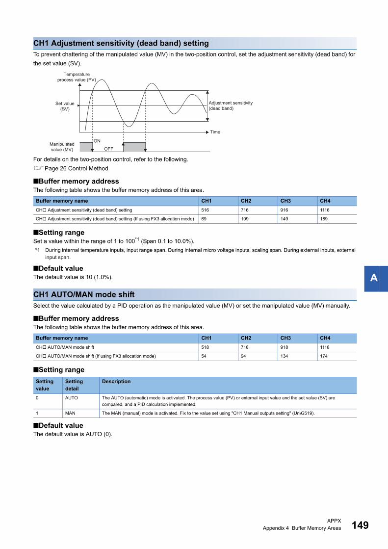
A
CH1 Adjustment sensitivity (dead band) settingTo prevent chattering of the manipulated value (MV) in the two-position control, set the adjustment sensitivity (dead band) for
the set value (SV).
For details on the two-position control, refer to the following.
Page 26 Control Method
■Buffer memory addressThe following table shows the buffer memory address of this area.
■Setting rangeSet a value within the range of 1 to 100*1 (Span 0.1 to 10.0%).
*1 During internal temperature inputs, input range span. During internal micro voltage inputs, scaling span. During external inputs, external input span.
■Default valueThe default value is 10 (1.0%).
CH1 AUTO/MAN mode shiftSelect the value calculated by a PID operation as the manipulated value (MV) or set the manipulated value (MV) manually.
■Buffer memory addressThe following table shows the buffer memory address of this area.
■Setting range
■Default valueThe default value is AUTO (0).
Buffer memory name CH1 CH2 CH3 CH4
CH Adjustment sensitivity (dead band) setting 516 716 916 1116
CH Adjustment sensitivity (dead band) setting (If using FX3 allocation mode) 69 109 149 189
Buffer memory name CH1 CH2 CH3 CH4
CH AUTO/MAN mode shift 518 718 918 1118
CH AUTO/MAN mode shift (If using FX3 allocation mode) 54 94 134 174
Setting value
Setting detail
Description
0 AUTO The AUTO (automatic) mode is activated. The process value (PV) or external input value and the set value (SV) are
compared, and a PID calculation implemented.
1 MAN The MAN (manual) mode is activated. Fix to the value set using "CH1 Manual outputs setting" (Un\G519).
ON
OFF
Temperatureprocess value (PV)
Set value(SV)
Manipulatedvalue (MV)
Time
Adjustment sensitivity (dead band)
APPXAppendix 4 Buffer Memory Areas 149
15
CH1 Manual output settingThis buffer memory area is used to set the manipulated value (MV) in the MAN mode.
Even though writing of data is executed during control in the AUTO mode, the setting values do not change.
■Buffer memory addressThe following table shows the buffer memory address of this area.
■How to shift the modeChange the mode with the following buffer memory area.
• 'CH1 AUTO/MAN mode shift' (Un\G518) (Page 149 CH1 AUTO/MAN mode shift)
■Setting range-50 to 1050 (-5.0 to 105.0%)
■Enabling the settingsCheck that "CH1 event (Un\G429)" in the Manual output settings is b13 before writing.
A value that has been written while MAN mode shift completion flag is OFF will be replaced with the manipulated value (MV)
that the system calculated using the PID operation.
■Default valueThe default value is -50 (-5.0%).
CH1 Cooling upper limit output limiterSet the upper limit value for actually outputting the manipulated value for cooling (MVc) calculated by the cooling and heating
PID operation to an external device. In the auto tuning, this setting is ignored.
■Buffer memory addressThe following table shows the buffer memory address of this area.
■Setting rangeThis is 0 to 1050 (0.0 to 105.0%).
In the heating-cooling PID control, the lower limit value is not used. When 'CH1 Lower limit output limiter'
(Un\G509) is set to a value other than 0, an out of setting range error (error code: 1950H) occurs.
■Two-position controlIn the two-position control, this setting is disabled.
■Default valueThe default value is 1000 (100.0%).
Buffer memory name CH1 CH2 CH3 CH4
CH Manual output setting 519 719 919 1119
CH Manual output setting (If using FX3 allocation mode) 55 95 135 175
Buffer memory name CH1 CH2 CH3 CH4
CH Cooling upper limit output limiter 521 721 921 1121
CH Cooling upper limit output limiter (If using FX3 allocation mode) 66 106 146 186
0APPXAppendix 4 Buffer Memory Areas
A
CH1 Cooling control output cycle settingSets the cooling control output cycle (time proportional cycle).
Cooling manipulated value (MVc) ON time and OFF time are each as described below.
• ON time: Cooling control output cycle (s) × cooling manipulated value (%)
• OFF time: Cooling control output cycle (s) × (100 - cooling manipulated value (%))
For details, refer to Page 142 CH1 Control output cycle setting.
■Buffer memory addressThe following table shows the buffer memory address of this area.
CH1 Cooling method settingSet a cooling control method in the heating-cooling PID control. Select a cooling method suitable for cooling characteristics of
devices.
For details on the cooling method setting function, refer to the following.
Page 35 Cooling Method Setting Function
■Buffer memory addressThe following table shows the buffer memory address of this area.
■Setting range • 0: Air cooling
• 1: Water cooling
• 2: Cooling gain linear
PID constant calculation results are effected by AT (auto tuning) depending on the settings, so set before
implementing AT (auto tuning).
■Default valueThe default value is 0 (air cooling).
Buffer memory name CH1 CH2 CH3 CH4
CH Cooling control output cycle setting 522 722 922 1122
CH Cooling control output cycle setting (If using FX3 allocation mode) 71 111 151 191
Buffer memory name CH1 CH2 CH3 CH4
CH Cooling method setting 523 723 923 1123
CH Cooling method setting (If using FX3 allocation mode) 232
APPXAppendix 4 Buffer Memory Areas 151
15
CH1 Overlap/dead band settingConfigure the overlap/dead band setting. For details on the overlap/dead band function, refer to the following.
Page 34 Overlap/dead Band Function
■Buffer memory addressThe following table shows the buffer memory address of this area.
■Setting range
*1 During internal temperature inputs, input range span. During internal micro voltage inputs, scaling span. During external inputs, external input span.
■Default valueThe default value is 0 (None).
CH1 Alert dead band settingThis setting is uses the alert function. This is the common setting for all channel alerts 1 to 4.
For details of the alert function, refer to the following.
Page 54 Alert Function
■Buffer memory addressThe following table shows the buffer memory address of this area.
■Setting range0 to 100 (span*1 0.0 to 10.0%)
*1 During internal temperature inputs, input range span. During internal micro voltage inputs, scaling span. During external inputs, external input span
■Default valueSet to 10 (1.0% of span).
Buffer memory name CH1 CH2 CH3 CH4
CH Overlap/dead band setting 524 724 924 1124
CH Overlap/dead band setting (If using FX3 allocation mode) 63 103 143 183
Setting value Description
-100 to -1 (span*1-10.0 to -0.1%) Overlap
0 None
1 to 100 (span*10.1 to 10.0%) Dead band
Buffer memory name CH1 CH2 CH3 CH4
CH Alert dead band setting 531 731 931 1131
Alert dead band setting (If using FX3 allocation mode) 233
2APPXAppendix 4 Buffer Memory Areas
A
CH1 Number of alert delaySet the number of times to execute sampling to judge an alert. This is the common setting for all channel alerts 1 to 4.
By setting the number of times to execute sampling, when the temperature process value (PV) stays within the alert range
after the temperature process value (PV) has entered the alert range until the number of times to execute sampling exceeds
the number of alert delay, an alert occurs. For details of the alert function, refer to the following.
Page 54 Alert Function
■Buffer memory addressThe following table shows the buffer memory address of this area.
■Setting rangeThe setting range is 0 to 30000 (times).
When 0 (times) has been set, an alert occurs as soon as the temperature process value (PV) goes within the
alert range.
■Default valueThe default value is 0 (times).
CH1 Alert 1 mode settingSet the alert mode of Alert 1. For details of the alert function, refer to the following.
Page 54 Alert Function
■Buffer memory addressThe following table shows the buffer memory address of this area.
■Alert mode and alert set valueSet an alert set value for the alert mode of Alert 1 selected in this setting. Set a value in 'CH1 Alert set value 1' (Un\G434).
'CH1 Alert set value 1' (Un\G434) corresponds to the alert mode of Alert 1.
Buffer memory name CH1 CH2 CH3 CH4
CH Number of alert delay 532 732 932 1132
Number of alert delay (If using FX3 allocation mode) 234
Buffer memory name CH1 CH2 CH3 CH4
CH Alert 1 mode setting 533 733 933 1133
CH Alert 1 mode setting (If using FX3 allocation mode) 209 215 221 227
APPXAppendix 4 Buffer Memory Areas 153
15
■Setting rangeThe following table lists setting values and setting ranges of alert set values in each alert mode.
*1 During internal temperature inputs, input range. During internal micro voltage inputs, scaling range. During external inputs, external input range.
*2 During internal temperature inputs, input range span. During internal micro voltage inputs, scaling span. During external inputs, external input span.
■Enabling the settingsIf changing the settings, turn OFF→ON→OFF the 'Settings change command' (Un\G399, b11) in normal mode to enable the
settings contents.
■Default valueThe default value is 0.
CH1 Alert 2 mode settingSet the alert mode of Alert 2. For details of the alert function, refer to the following.
Page 54 Alert Function
■Buffer memory addressThe following table shows the buffer memory address of this area.
■Alert mode and alert set valueSet an alert set value for the alert mode of Alert 2 selected in this setting. Set a value in 'CH1 Alert set value 2' (Un\G435).
'CH1 Alert set value 2' (Un\G435) corresponds to the alert mode of Alert 2.
■Setting rangeFor the setting range, refer to the following in CH1 Alert 1 mode setting.
Page 154 Setting range
■Enabling the settingsFor enabling the settings, refer to the following in CH1 Alert 1 mode setting.
Page 154 Enabling the settings
■Default valueFor the default value, refer to the following in CH1 Alert 1 mode setting.
Page 154 Default value
Setting value
Alert mode Setting range of alert set value
0 No alert (Alert not implemented)
1 Upper limit input alert Value within set input range*1
2 Lower limit input alert
3 Upper limit deviation alert - span to + span*2
4 Lower limit deviation alert
5 Upper/lower limit deviation alert 0 to + span*2
6 Within-range alert
7 Upper limit input alert with wait Value within set input range*1
8 Lower limit input alert with wait
9 Upper limit deviation alert with wait - span to + span*2
10 Lower limit deviation alert with wait
11 Upper/lower limit deviation alert with wait 0 to + span*2
12 Upper limit deviation alert with re-wait - span to + span*2
13 Lower limit deviation alert with re-wait
14 Upper/lower limit deviation alert with re-wait 0 to + span*2
Buffer memory name CH1 CH2 CH3 CH4
CH Alert 2 mode setting 534 734 934 1134
CH Alert 2 mode setting (If using FX3 allocation mode) 210 216 222 228
4APPXAppendix 4 Buffer Memory Areas
A
CH1 Alert 3 mode settingSet the alert mode of Alert 3. For details of the alert function, refer to the following.
Page 54 Alert Function
■Buffer memory addressThe following table shows the buffer memory address of this area.
■Alert mode and alert set valueSet an alert set value for the alert mode of Alert 3 selected in this setting. Set a value in 'CH1 Alert set value 3' (Un\G436).
'CH1 Alert set value 3' (Un\G436) corresponds to the alert mode of Alert 3.
■Setting rangeFor the setting range, refer to the following in CH1 Alert 1 mode setting.
Page 154 Setting range
■Enabling the settingsFor enabling the settings, refer to the following in CH1 Alert 1 mode setting.
Page 154 Enabling the settings
■Default valueFor the default value, refer to the following in CH1 Alert 1 mode setting.
Page 154 Default value
CH1 Alert 4 mode settingSet the alert mode of Alert 4. For details of the alert function, refer to the following.
Page 54 Alert Function
■Buffer memory addressThe following table shows the buffer memory address of this area.
■Alert mode and alert set valueSet an alert set value for the alert mode of Alert 4 selected in this setting. Set a value in 'CH1 Alert set value 4' (Un\G437).
'CH1 Alert set value 4' (Un\G437) corresponds to the alert mode of Alert 4.
■Setting rangeFor the setting range, refer to the following in CH1 Alert 1 mode setting.
Page 154 Setting range
■Enabling the settingsFor enabling the settings, refer to the following in CH1 Alert 1 mode setting.
Page 154 Enabling the settings
■Default valueFor the default value, refer to the following in CH1 Alert 1 mode setting.
Page 154 Default value
Buffer memory name CH1 CH2 CH3 CH4
CH Alert 3 mode setting 535 735 935 1135
CH Alert 3 mode setting (If using FX3 allocation mode) 211 217 223 229
Buffer memory name CH1 CH2 CH3 CH4
CH Alert 4 mode setting 536 736 936 1136
CH Alert 4 mode setting (If using FX3 allocation mode) 212 218 224 230
APPXAppendix 4 Buffer Memory Areas 155
15
CH1 Loop disconnection detection judgment timeSet the loop disconnection detection judgment time constant.
For loop disconnections, the amount of change to the process value (PV) is detected for each loop disconnection detection
judgment time from when the manipulated value (MV) is either 100% (or the upper limit output limiter) or greater, or 0% (or the
lower limit output limiter) or lower, and the loop disconnection alert turns ON when it is judged that a control loop error has
occurred. For details of the loop disconnection detection function, refer to the following.
Page 61 Loop Disconnection Detection Function
■Buffer memory addressThe following table shows the buffer memory address of this area.
■Setting rangeThe setting range is 0 to 7200 (s). Set to 0 to turn OFF this function.
■When executing the auto tuningA value that is twice as large as the value in 'CH1 Integral time (I) setting' (Un\G432) is automatically set in this setting.
■Default valueThe default value is 480 (s).
CH1 Loop disconnection detection dead bandSet the non-alert area having the set value (SV) at the center (temperature width in which no loop disconnection is detected)
to prevent accidental alerts of the loop disconnection detection.
For details on the loop disconnection detection function, refer to the following.
Page 61 Loop Disconnection Detection Function
■Buffer memory addressThe following table shows the buffer memory address of this area.
■Setting range0 to input span*1
*1 During internal temperature inputs, input range span. During internal micro voltage inputs, scaling span. During external inputs, external input span.
■Setting unitThe value to be set differs depending on the value stored in 'CH1 Decimal point position' (Un\G400).
• No decimal point (0): Set a value in increments of 1 ( or digit).
• If there is 1 digit (1) past the decimal point: Set a value (the value multiplied by 10) in increments of 0.1 ().
■Default valueThe default value is 0.
Buffer memory name CH1 CH2 CH3 CH4
CH Loop disconnection detection judgment time 537 737 937 1137
CH Loop disconnection detection judgment time (If using FX3 allocation
mode)
78 118 158 198
Buffer memory name CH1 CH2 CH3 CH4
CH Loop disconnection detection dead band 538 738 938 1138
CH Loop disconnection detection dead band (If using FX3 allocation mode) 79 119 159 199
6APPXAppendix 4 Buffer Memory Areas
A
CH1 AT biasIf the process value (PV) does not exceed the set value (SV) during auto tuning implementation, AT bias is set.
For details of the AT (auto tuning) function, refer to the following.
Page 40 AT (Auto Tuning) Bias Function
■Buffer memory addressThe following table shows the buffer memory address of this area.
■Setting range- span to + span*1 (If span exceeds 32767, the span becomes -322768 to +322767.)
*1 During internal temperature inputs, input range span. During internal micro voltage inputs, scaling span. During external inputs, external input span.
■Setting unitThe value to be set differs depending on the value stored in 'CH1 Decimal point position' (Un\G400).
• No decimal point (0): Set a value in increments of 1 ( or digit).
• If there is 1 digit (1) past the decimal point: Set a value (the value multiplied by 10) in increments of 0.1 ().
■Default valueThe default value is 0.
CH1 Startup tuning settingSets stop/implement startup tuning.
For details of the startup tuning function, refer to the following.
Page 41 Startup Tuning Function
■Buffer memory addressThe following table shows the buffer memory address of this area.
■Setting range • 0: Stop startup tuning
• 1: Implement startup tuning
■Default valueSet to 0 (Stop startup tuning).
Precautions
Auto tuning is implemented if control is started when both the 'auto tuning command' (Un\G399, b4) and 'startup tuning
implementation command' (Un\G548) status is "1".
Buffer memory name CH1 CH2 CH3 CH4
CH AT bias 546 746 946 1146
CH AT bias (If using FX3 allocation mode) 74 114 154 194
Buffer memory name CH1 CH2 CH3 CH4
CH Startup tuning setting 548 748 948 1148
CH Startup tuning setting (If using FX3 allocation mode) 87 127 167 207
APPXAppendix 4 Buffer Memory Areas 157
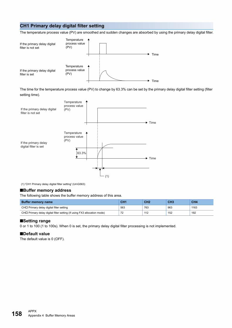
15
CH1 Primary delay digital filter settingThe temperature process value (PV) are smoothed and sudden changes are absorbed by using the primary delay digital filter.
The time for the temperature process value (PV) to change by 63.3% can be set by the primary delay digital filter setting (filter
setting time).
■Buffer memory addressThe following table shows the buffer memory address of this area.
■Setting range0 or 1 to 100 (1 to 100s). When 0 is set, the primary delay digital filter processing is not implemented.
■Default valueThe default value is 0 (OFF).
(1) 'CH1 Primary delay digital filter setting' (Un\G563)
Buffer memory name CH1 CH2 CH3 CH4
CH Primary delay digital filter setting 563 763 963 1163
CH Primary delay digital filter setting (If using FX3 allocation mode) 72 112 152 192
Time
Time
Temperature process value (PV)
Temperature process value (PV)
If the primary delay digital filter is not set
If the primary delay digital filter is set
63.3%
(1)
Time
Time
Temperature process value (PV)
Temperature process value (PV)
If the primary delay digital filter is set
If the primary delay digital filter is not set
8APPXAppendix 4 Buffer Memory Areas
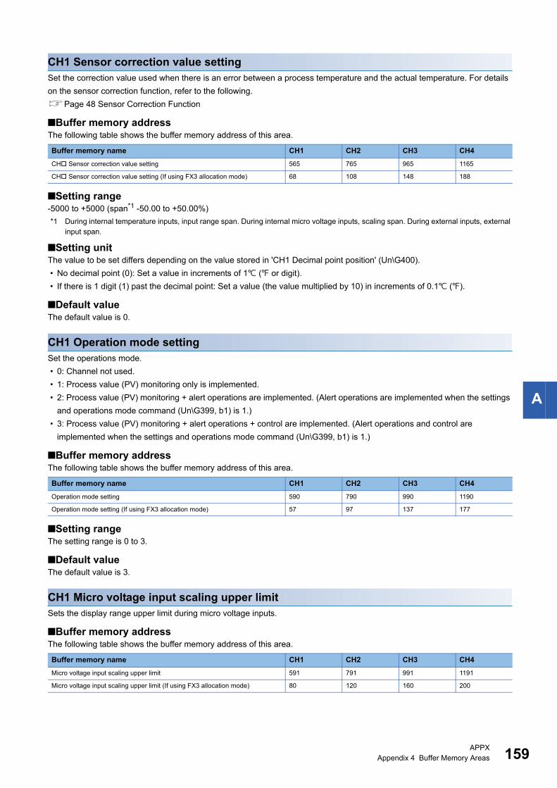
A
CH1 Sensor correction value settingSet the correction value used when there is an error between a process temperature and the actual temperature. For details
on the sensor correction function, refer to the following.
Page 48 Sensor Correction Function
■Buffer memory addressThe following table shows the buffer memory address of this area.
■Setting range-5000 to +5000 (span*1 -50.00 to +50.00%)
*1 During internal temperature inputs, input range span. During internal micro voltage inputs, scaling span. During external inputs, external input span.
■Setting unitThe value to be set differs depending on the value stored in 'CH1 Decimal point position' (Un\G400).
• No decimal point (0): Set a value in increments of 1 ( or digit).
• If there is 1 digit (1) past the decimal point: Set a value (the value multiplied by 10) in increments of 0.1 ().
■Default valueThe default value is 0.
CH1 Operation mode settingSet the operations mode.
• 0: Channel not used.
• 1: Process value (PV) monitoring only is implemented.
• 2: Process value (PV) monitoring + alert operations are implemented. (Alert operations are implemented when the settings
and operations mode command (Un\G399, b1) is 1.)
• 3: Process value (PV) monitoring + alert operations + control are implemented. (Alert operations and control are
implemented when the settings and operations mode command (Un\G399, b1) is 1.)
■Buffer memory addressThe following table shows the buffer memory address of this area.
■Setting rangeThe setting range is 0 to 3.
■Default valueThe default value is 3.
CH1 Micro voltage input scaling upper limitSets the display range upper limit during micro voltage inputs.
■Buffer memory addressThe following table shows the buffer memory address of this area.
Buffer memory name CH1 CH2 CH3 CH4
CH Sensor correction value setting 565 765 965 1165
CH Sensor correction value setting (If using FX3 allocation mode) 68 108 148 188
Buffer memory name CH1 CH2 CH3 CH4
Operation mode setting 590 790 990 1190
Operation mode setting (If using FX3 allocation mode) 57 97 137 177
Buffer memory name CH1 CH2 CH3 CH4
Micro voltage input scaling upper limit 591 791 991 1191
Micro voltage input scaling upper limit (If using FX3 allocation mode) 80 120 160 200
APPXAppendix 4 Buffer Memory Areas 159
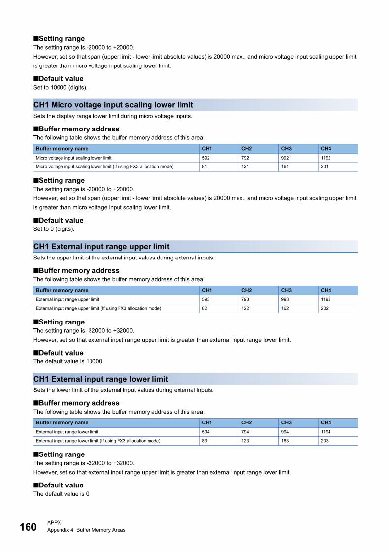
16
■Setting rangeThe setting range is -20000 to +20000.
However, set so that span (upper limit - lower limit absolute values) is 20000 max., and micro voltage input scaling upper limit
is greater than micro voltage input scaling lower limit.
■Default valueSet to 10000 (digits).
CH1 Micro voltage input scaling lower limitSets the display range lower limit during micro voltage inputs.
■Buffer memory addressThe following table shows the buffer memory address of this area.
■Setting rangeThe setting range is -20000 to +20000.
However, set so that span (upper limit - lower limit absolute values) is 20000 max., and micro voltage input scaling upper limit
is greater than micro voltage input scaling lower limit.
■Default valueSet to 0 (digits).
CH1 External input range upper limitSets the upper limit of the external input values during external inputs.
■Buffer memory addressThe following table shows the buffer memory address of this area.
■Setting rangeThe setting range is -32000 to +32000.
However, set so that external input range upper limit is greater than external input range lower limit.
■Default valueThe default value is 10000.
CH1 External input range lower limitSets the lower limit of the external input values during external inputs.
■Buffer memory addressThe following table shows the buffer memory address of this area.
■Setting rangeThe setting range is -32000 to +32000.
However, set so that external input range upper limit is greater than external input range lower limit.
■Default valueThe default value is 0.
Buffer memory name CH1 CH2 CH3 CH4
Micro voltage input scaling lower limit 592 792 992 1192
Micro voltage input scaling lower limit (If using FX3 allocation mode) 81 121 161 201
Buffer memory name CH1 CH2 CH3 CH4
External input range upper limit 593 793 993 1193
External input range upper limit (If using FX3 allocation mode) 82 122 162 202
Buffer memory name CH1 CH2 CH3 CH4
External input range lower limit 594 794 994 1194
External input range lower limit (If using FX3 allocation mode) 83 123 163 203
0APPXAppendix 4 Buffer Memory Areas
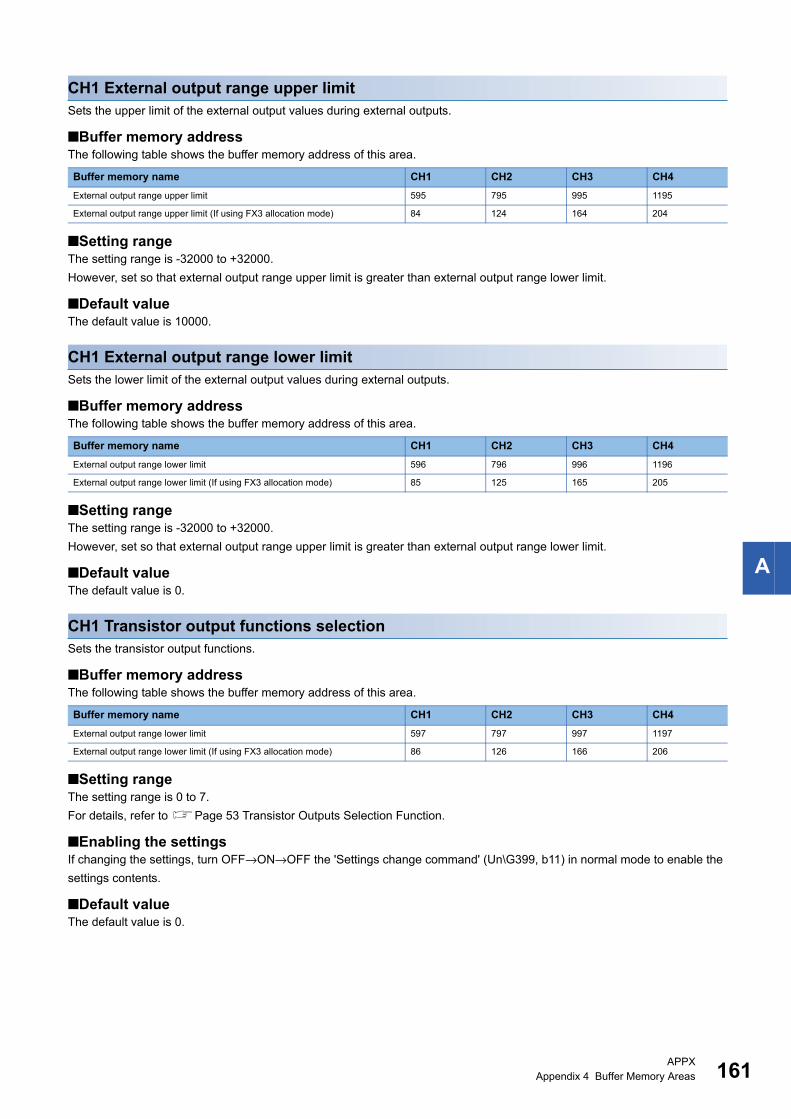
A
CH1 External output range upper limitSets the upper limit of the external output values during external outputs.
■Buffer memory addressThe following table shows the buffer memory address of this area.
■Setting rangeThe setting range is -32000 to +32000.
However, set so that external output range upper limit is greater than external output range lower limit.
■Default valueThe default value is 10000.
CH1 External output range lower limitSets the lower limit of the external output values during external outputs.
■Buffer memory addressThe following table shows the buffer memory address of this area.
■Setting rangeThe setting range is -32000 to +32000.
However, set so that external output range upper limit is greater than external output range lower limit.
■Default valueThe default value is 0.
CH1 Transistor output functions selectionSets the transistor output functions.
■Buffer memory addressThe following table shows the buffer memory address of this area.
■Setting rangeThe setting range is 0 to 7.
For details, refer to Page 53 Transistor Outputs Selection Function.
■Enabling the settingsIf changing the settings, turn OFF→ON→OFF the 'Settings change command' (Un\G399, b11) in normal mode to enable the
settings contents.
■Default valueThe default value is 0.
Buffer memory name CH1 CH2 CH3 CH4
External output range upper limit 595 795 995 1195
External output range upper limit (If using FX3 allocation mode) 84 124 164 204
Buffer memory name CH1 CH2 CH3 CH4
External output range lower limit 596 796 996 1196
External output range lower limit (If using FX3 allocation mode) 85 125 165 205
Buffer memory name CH1 CH2 CH3 CH4
External output range lower limit 597 797 997 1197
External output range lower limit (If using FX3 allocation mode) 86 126 166 206
APPXAppendix 4 Buffer Memory Areas 161
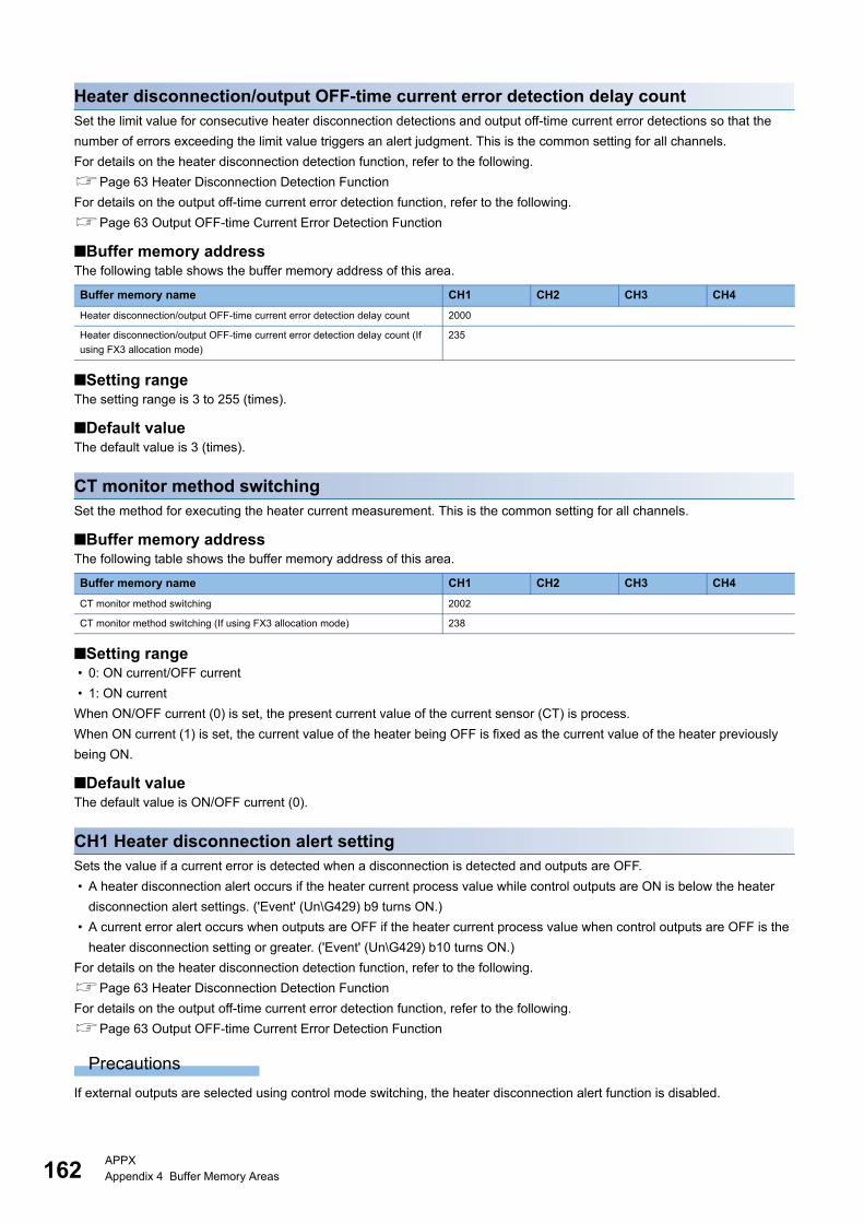
16
Heater disconnection/output OFF-time current error detection delay countSet the limit value for consecutive heater disconnection detections and output off-time current error detections so that the
number of errors exceeding the limit value triggers an alert judgment. This is the common setting for all channels.
For details on the heater disconnection detection function, refer to the following.
Page 63 Heater Disconnection Detection Function
For details on the output off-time current error detection function, refer to the following.
Page 63 Output OFF-time Current Error Detection Function
■Buffer memory addressThe following table shows the buffer memory address of this area.
■Setting rangeThe setting range is 3 to 255 (times).
■Default valueThe default value is 3 (times).
CT monitor method switchingSet the method for executing the heater current measurement. This is the common setting for all channels.
■Buffer memory addressThe following table shows the buffer memory address of this area.
■Setting range • 0: ON current/OFF current
• 1: ON current
When ON/OFF current (0) is set, the present current value of the current sensor (CT) is process.
When ON current (1) is set, the current value of the heater being OFF is fixed as the current value of the heater previously
being ON.
■Default valueThe default value is ON/OFF current (0).
CH1 Heater disconnection alert settingSets the value if a current error is detected when a disconnection is detected and outputs are OFF.
• A heater disconnection alert occurs if the heater current process value while control outputs are ON is below the heater
disconnection alert settings. ('Event' (Un\G429) b9 turns ON.)
• A current error alert occurs when outputs are OFF if the heater current process value when control outputs are OFF is the
heater disconnection setting or greater. ('Event' (Un\G429) b10 turns ON.)
For details on the heater disconnection detection function, refer to the following.
Page 63 Heater Disconnection Detection Function
For details on the output off-time current error detection function, refer to the following.
Page 63 Output OFF-time Current Error Detection Function
Precautions
If external outputs are selected using control mode switching, the heater disconnection alert function is disabled.
Buffer memory name CH1 CH2 CH3 CH4
Heater disconnection/output OFF-time current error detection delay count 2000
Heater disconnection/output OFF-time current error detection delay count (If
using FX3 allocation mode)
235
Buffer memory name CH1 CH2 CH3 CH4
CT monitor method switching 2002
CT monitor method switching (If using FX3 allocation mode) 238
2APPXAppendix 4 Buffer Memory Areas
A
■Buffer memory addressThe following table shows the buffer memory address of this area.
■Setting range0 to 1000 (0.0 to 100.0 A).
When 0 is set, heater disconnection detections and output off-time current error detections are not executed.
■Default valueThe default value is 0 (A).
CH1 Heater current process valueStores the heater current value detected by the temperature control module.
■Buffer memory addressThe following table shows the buffer memory address of this area.
Precautions
If control mode comprising external outputs using control mode switching is selected,*1 CT inputs are not processed. 0 is
normally stored in the heater current process value.
*1 If control mode is 2, 3, 6, 7, all channels are normally 0.If control mode is 4 or 5, only channels 2 and 4 are normally 0.
CH1 CT ratio settingSet the number of second-winding (turns) of the current sensor (CT) to be connected. This is the common setting for all
channels if using FX3 allocation mode.
■Buffer memory addressThe following table shows the buffer memory address of this area.
■Setting rangeThe setting range is 1 to 9999.
Set the value to satisfy the following.
(Max. process current value (effective value)*1 × 1.1 ÷ CT ratio setting (CT secondary winding count used)) ≤ 0.1377
*1 Max. process current value (effective value) ≤ 100 A
Ex.
If CT ratio setting is 800, and the max. process current value (effective value) is 100 A, the left hand side = 0.1375, and the
conditions are satisfied, so measuring up to 100 A is possible.
• Current sensor (CT) reference examples
■Default valueThe default value is 800.
Buffer memory name CH1 CH2 CH3 CH4
CH Heater disconnection alert setting 2004 2007 2010 2013
CH Heater disconnection alert setting (If using FX3 allocation mode) 53 93 133 173
Buffer memory name CH1 CH2 CH3 CH4
CH Heater current process value 2030 2031 2032 2033
CH Heater current process value (If using FX3 allocation mode) 21 22 23 24
Buffer memory name CH1 CH2 CH3 CH4
CH CT ratio setting 2062 2063 2064 2065
CH CT ratio setting (If using FX3 allocation mode) 239
CT model name CT ratio set value
CTL-6-P-H/CTL-6-S-H/CTL-6-P 800
CTL-12-S36-8/CTL-12L-8 800
CTL-12-S56-10/CTL-12-S36-10 1000
APPXAppendix 4 Buffer Memory Areas 163
16
Error historyUp to 16 errors that occurred in the module are recorded.
*1 Value stored when an error occurs at 12:34:56.789 on Monday, June 30, 2014
■Buffer memory addressThe following table shows the buffer memory address of this area.
Item Stored contents Storage example*1
First two digits of the year/last
two digits of the year
Stored in BCD code. 2014H
Month/day 630H
Hour/minute 1234H
Second 56H
Day of the week One of the following values is stored in BCD code.
Sunday: 0, Monday: 1, Tuesday: 2, Wednesday: 3, Thursday: 4, Friday: 5, Saturday: 6
1H
Millisecond (upper) Stored in BCD code. 7H
Millisecond (lower) 89H
Buffer memory name CH1 CH2 CH3 CH4
Error history 3600 to 3759
Error history (If using FX3 allocation mode) 3600 to 3759
b15 to tob8 b7 b0
…
Error code
System area
First 2 digits of date Last 2 digits of dateMonth DayTime Minute
SecondMillisecond (upper)
Day of the weekMillisecond (lower)
Un\G3600
Un\G3604Un\G3603Un\G3602Un\G3601
Un\G3605Un\G3606
Un\G3609
4APPXAppendix 4 Buffer Memory Areas
A
Alarm historyUp to 16 alarms that occurred in the module are recorded.
*1 Value stored when an alarm occurs at 12:34:56.789 on Monday, June 30, 2014
■Buffer memory addressThe following table shows the buffer memory address of this area.
Item Stored contents Storage example*1
First two digits of the year/last
two digits of the year
Stored in BCD code. 2014H
Month/day 630H
Hour/minute 1234H
Second 56H
Day of the week One of the following values is stored in BCD code.
Sunday: 0, Monday: 1, Tuesday: 2, Wednesday: 3, Thursday: 4, Friday: 5, Saturday: 6
1H
Millisecond (upper) Stored in BCD code. 7H
Millisecond (lower) 89H
Buffer memory name CH1 CH2 CH3 CH4
Alarm history 3760 to 3919
Alarm history (If using FX3 allocation mode) 3760 to 3919
b15 to tob8 b7 b0Alarm code
First 2 digits of date Last 2 digits of dateMonth DayTime Minute
Second Day of the week
Un\G3760
Un\G3764Un\G3763Un\G3762Un\G3761
Un\G3766
Un\G3769System area
Millisecond (upper) Millisecond (lower)Un\G3765
…
APPXAppendix 4 Buffer Memory Areas 165
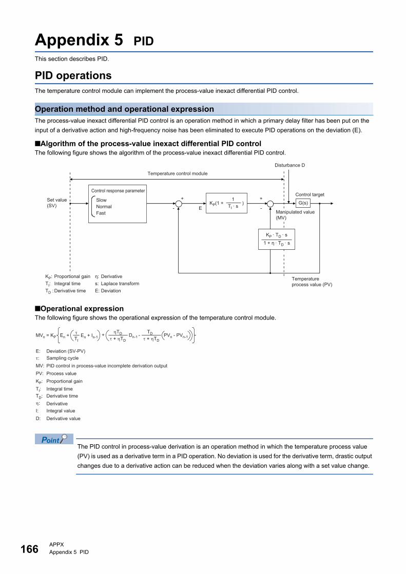
16
Appendix 5 PIDThis section describes PID.
PID operationsThe temperature control module can implement the process-value inexact differential PID control.
Operation method and operational expressionThe process-value inexact differential PID control is an operation method in which a primary delay filter has been put on the
input of a derivative action and high-frequency noise has been eliminated to execute PID operations on the deviation (E).
■Algorithm of the process-value inexact differential PID controlThe following figure shows the algorithm of the process-value inexact differential PID control.
■Operational expressionThe following figure shows the operational expression of the temperature control module.
The PID control in process-value derivation is an operation method in which the temperature process value
(PV) is used as a derivative term in a PID operation. No deviation is used for the derivative term, drastic output
changes due to a derivative action can be reduced when the deviation varies along with a set value change.
+
-
+
-
KP · TD · s
1 + η · TD · s
1KP(1 + )TI · s
G(s)
s: E:
η: KP: TI: TD :
E
Control targetSlowNormalFast
Disturbance D
Temperature process value (PV)Laplace transform
Deviation
DerivativeProportional gainIntegral timeDerivative time
Set value (SV)
Control response parameter
Manipulated value(MV)
Temperature control module
MVn = KP En +TD
MV:PV:
TD:
TI
En + In-1 + TD
TD + TD
Dn-1 -+ PVn - PVn-1
:E:
:
D:I:
KP:TI:
Sampling cycleDeviation (SV-PV)
Derivative
Derivative valueIntegral value
PID control in process-value incomplete derivation output
Derivative time Integral time
Process valueProportional gain
6APPXAppendix 5 PID
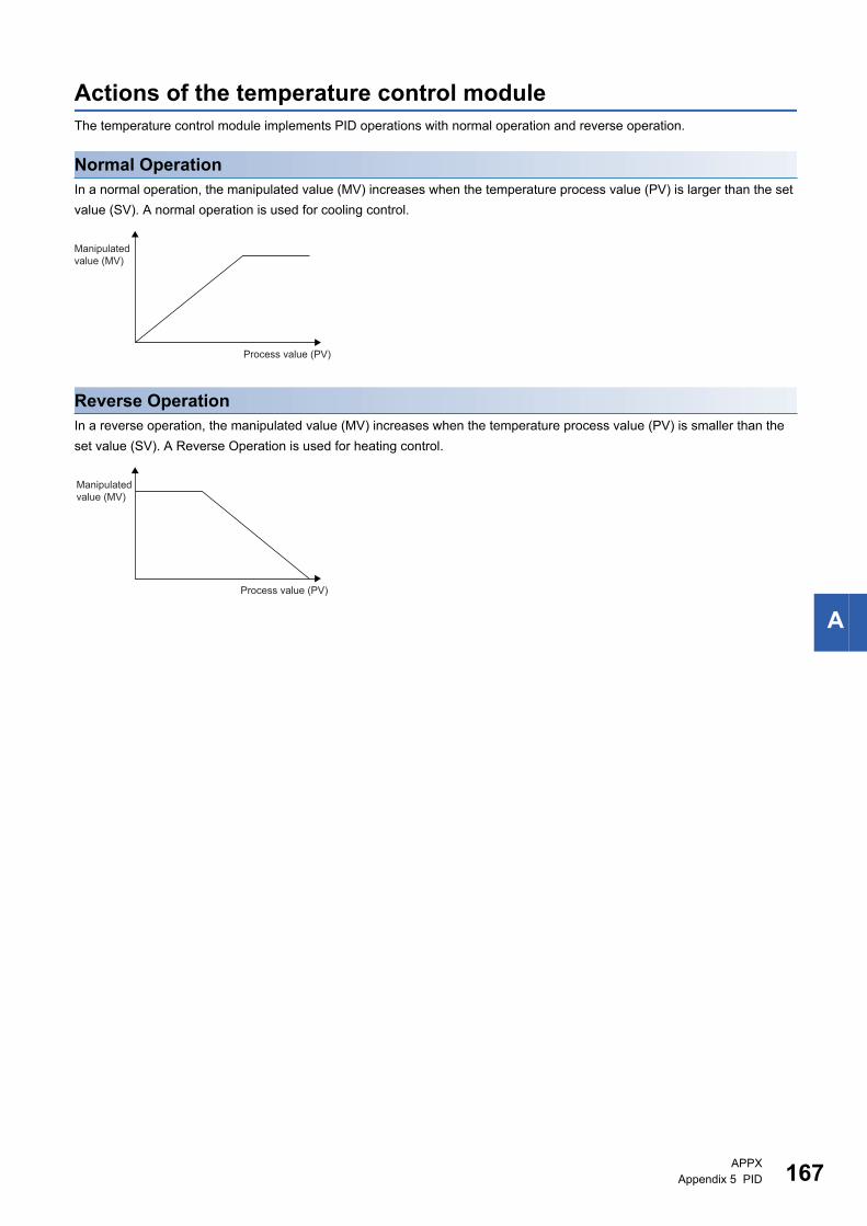
A
Actions of the temperature control moduleThe temperature control module implements PID operations with normal operation and reverse operation.
Normal OperationIn a normal operation, the manipulated value (MV) increases when the temperature process value (PV) is larger than the set
value (SV). A normal operation is used for cooling control.
Reverse OperationIn a reverse operation, the manipulated value (MV) increases when the temperature process value (PV) is smaller than the
set value (SV). A Reverse Operation is used for heating control.
Manipulatedvalue (MV)
Process value (PV)
Manipulatedvalue (MV)
Process value (PV)
APPXAppendix 5 PID 167
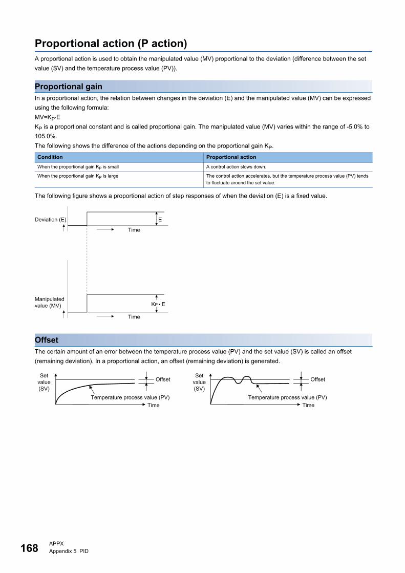
16
Proportional action (P action)A proportional action is used to obtain the manipulated value (MV) proportional to the deviation (difference between the set
value (SV) and the temperature process value (PV)).
Proportional gainIn a proportional action, the relation between changes in the deviation (E) and the manipulated value (MV) can be expressed
using the following formula:
MV=KP⋅EKP is a proportional constant and is called proportional gain. The manipulated value (MV) varies within the range of -5.0% to
105.0%.
The following shows the difference of the actions depending on the proportional gain KP.
The following figure shows a proportional action of step responses of when the deviation (E) is a fixed value.
OffsetThe certain amount of an error between the temperature process value (PV) and the set value (SV) is called an offset
(remaining deviation). In a proportional action, an offset (remaining deviation) is generated.
Condition Proportional action
When the proportional gain KP is small A control action slows down.
When the proportional gain KP is large The control action accelerates, but the temperature process value (PV) tends
to fluctuate around the set value.
E
Time
Time
Deviation (E)
Manipulatedvalue (MV) KP E
Setvalue(SV)
Setvalue(SV)
Temperature process value (PV) Temperature process value (PV)
Offset
TimeTime
Offset
8APPXAppendix 5 PID
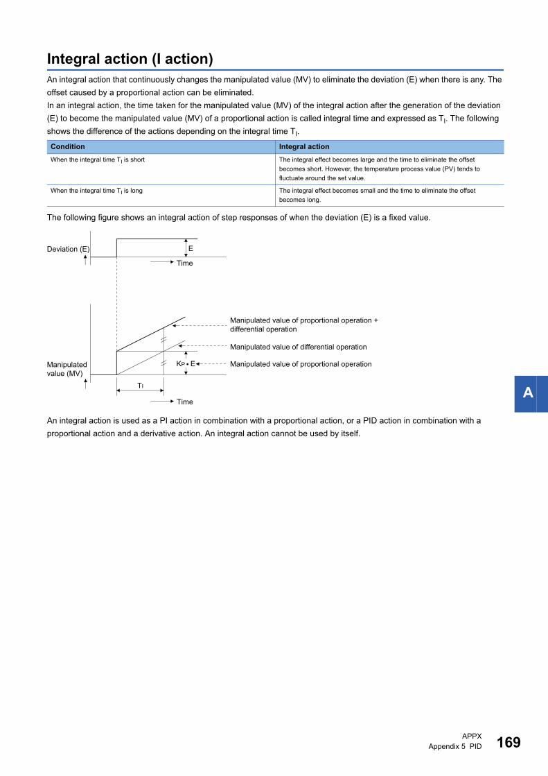
A
Integral action (I action)An integral action that continuously changes the manipulated value (MV) to eliminate the deviation (E) when there is any. The
offset caused by a proportional action can be eliminated.
In an integral action, the time taken for the manipulated value (MV) of the integral action after the generation of the deviation
(E) to become the manipulated value (MV) of a proportional action is called integral time and expressed as TI. The following
shows the difference of the actions depending on the integral time TI.
The following figure shows an integral action of step responses of when the deviation (E) is a fixed value.
An integral action is used as a PI action in combination with a proportional action, or a PID action in combination with a
proportional action and a derivative action. An integral action cannot be used by itself.
Condition Integral action
When the integral time TI is short The integral effect becomes large and the time to eliminate the offset
becomes short. However, the temperature process value (PV) tends to
fluctuate around the set value.
When the integral time TI is long The integral effect becomes small and the time to eliminate the offset
becomes long.
E
Manipulated value of proportional operation
Manipulated value of differential operation
Manipulated value of proportional operation + differential operation
Time
Time
Deviation (E)
Manipulatedvalue (MV)
KP E
TI
APPXAppendix 5 PID 169
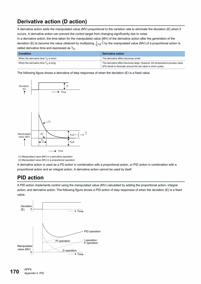
17
Derivative action (D action)A derivative action adds the manipulated value (MV) proportional to the variation rate to eliminate the deviation (E) when it
occurs. A derivative action can prevent the control target from changing significantly due to noise.
In a derivative action, the time taken for the manipulated value (MV) of the derivative action after the generation of the
deviation (E) to become the value obtained by multiplying by the manipulated value (MV) of a proportional action is
called derivative time and expressed as TD.
The following figure shows a derivative of step responses of when the deviation (E) is a fixed value.
A derivative action is used as a PD action in combination with a proportional action, or PID action in combination with a
proportional action and an integral action. A derivative action cannot be used by itself.
PID actionA PID action implements control using the manipulated value (MV) calculated by adding the proportional action, integral
action, and derivative action. The following figure shows a PID action of step responses of when the deviation (E) is a fixed
value.
Condition Derivative action
When the derivative time TD is short The derivative effect becomes small.
When the derivative time TD is long The derivative effect becomes large. However, the temperature process value
(PV) tends to fluctuate around the set value in short cycles.
(1) Manipulated value (MV) in a derivative operation
(2) Manipulated value (MV) in a proportional operation
×e η1 η
1-
(2)
TD KPE
KPE × × e
(1)
η1 η
1-
E
Time
Time
Manipulatedvalue (MV)
Deviation (E)
PID operation
I operationP operation
D operation
PI operation
Time
Time
Deviation(E)
Manipulated value (MV)
0APPXAppendix 5 PID
INDEX
I
A
Alarm history . . . . . . . . . . . . . . . . . . . . . . . . . 165Alert with re-wait . . . . . . . . . . . . . . . . . . . . . . . . 58Alert with wait . . . . . . . . . . . . . . . . . . . . . . . . . . 57Automatic setting at input range change . . . . . . 120Automatic setting monitor at input range change 119
C
Cascade bias . . . . . . . . . . . . . . . . . . . . . . . . . 122Cascade gain . . . . . . . . . . . . . . . . . . . . . . . . . 122Cascade monitor. . . . . . . . . . . . . . . . . . . . . . . 122Cascade ON/OFF . . . . . . . . . . . . . . . . . . . . . . 121CH1 Adjustment sensitivity (dead band) setting . 149CH1 Alert 1 mode setting . . . . . . . . . . . . . . . . . 153CH1 Alert 2 mode setting . . . . . . . . . . . . . . . . . 154CH1 Alert 3 mode setting . . . . . . . . . . . . . . . . . 155CH1 Alert 4 mode setting . . . . . . . . . . . . . . . . . 155CH1 Alert dead band setting . . . . . . . . . . . . . . 152CH1 Alert definition . . . . . . . . . . . . . . . . . . . . . 128CH1 Alert set value 1. . . . . . . . . . . . . . . . . . . . 137CH1 Alert set value 2. . . . . . . . . . . . . . . . . . . . 138CH1 Alert set value 3. . . . . . . . . . . . . . . . . . . . 139CH1 Alert set value 4. . . . . . . . . . . . . . . . . . . . 139CH1 AT bias. . . . . . . . . . . . . . . . . . . . . . . . . . 157CH1 AUTO/MAN mode shift . . . . . . . . . . . . . . . 149CH1 Control output cycle setting. . . . . . . . . . . . 142CH1 Control response parameter . . . . . . . . . . . 143CH1 Cooling control output cycle setting . . . . . . 151CH1 Cooling method setting. . . . . . . . . . . . . . . 151CH1 Cooling proportional band (Pc) setting . . . . 140CH1 Cooling transistor output flag. . . . . . . . . . . 133CH1 Cooling upper limit output limiter . . . . . . . . 150CH1 CT ratio setting . . . . . . . . . . . . . . . . . . . . 163CH1 Decimal point position . . . . . . . . . . . . . . . 128CH1 Derivative time (D) setting. . . . . . . . . . . . . 137CH1 Event . . . . . . . . . . . . . . . . . . . . . . . . . . . 134CH1 External input range lower limit . . . . . . . . . 160CH1 External input range upper limit . . . . . . . . . 160CH1 External output range lower limit . . . . . . . . 161CH1 External output range upper limit . . . . . . . . 161CH1 Heater current process value . . . . . . . . . . 163CH1 Heater disconnection alert setting . . . . . . . 162CH1 Heating control output cycle setting . . . . . . 142CH1 Heating proportional band (Ph) setting . . . . 136CH1 Heating transistor output flag . . . . . . . . . . 131CH1 Heating upper limit output limiter . . . . . . . . 145CH1 Input range . . . . . . . . . . . . . . . . . . . . . . . 140CH1 Integral time (I) setting . . . . . . . . . . . . . . . 136CH1 Loop disconnection detection dead band . . 156CH1 Loop disconnection detection judgment time . 156CH1 Lower limit output limiter . . . . . . . . . . . . . . 145CH1 Lower limit setting limiter . . . . . . . . . . . . . 147CH1 Manipulated value (MV) . . . . . . . . . . . . . . 129CH1 Manipulated value (MV) for output with another (external) analog module . . . . . . . . . . . . . . . . . 132CH1 Manipulated value for cooling (MVc) . . . . . 133CH1 Manipulated value for cooling (MVc) for output with another (external) analog module . . . . . . . . . . . 133CH1 Manipulated value for heating (MVh) . . . . . 129
CH1 Manipulated value for heating (MVh) for output with another (external) analog module . . . . . . . . . . . .132CH1 Manual output setting . . . . . . . . . . . . . . . .150CH1 Micro voltage input scaling lower limit . . . . .160CH1 Micro voltage input scaling upper limit . . . . .159CH1 Normal/Reverse operation setting . . . . . . . .148CH1 Number of alert delay . . . . . . . . . . . . . . . .153CH1 Operation mode setting . . . . . . . . . . . . . . .159CH1 Output change ratio limiter . . . . . . . . . . . . .146CH1 Overlap/dead band setting . . . . . . . . . . . . .152CH1 Primary delay digital filter setting. . . . . . . . .158CH1 Proportional band (P) setting . . . . . . . . . . .135CH1 Sensor correction value setting . . . . . . . . . .159CH1 Set value (SV) monitor. . . . . . . . . . . . . . . .132CH1 Set value (SV) setting . . . . . . . . . . . . . . . .135CH1 Setting change rate limiter . . . . . . . . . . . . .148CH1 Startup tuning setting. . . . . . . . . . . . . . . . .157CH1 Temperature process value (PV). . . . . . . . .129CH1 Temperature process value (PV) for input with another (external) analog module . . . . . . . . . . . .140CH1 Temperature rise completion range setting. .143CH1 Temperature rise completion soak time setting. . . . . . . . . . . . . . . . . . . . . . . . . . . . . . . . . . . .144CH1 Temperature rise judgment flag . . . . . . . . .130CH1 Transistor output flag (Control output flag) . .131CH1 Transistor output functions selection . . . . . .161CH1 Upper limit output limiter . . . . . . . . . . . . . .144CH1 Upper limit setting limiter . . . . . . . . . . . . . .147Control mode selection . . . . . . . . . . . . . . . . . . .119Control mode selection monitor . . . . . . . . . . . . .118CT monitor method switching. . . . . . . . . . . . . . .162
D
Deviation alert . . . . . . . . . . . . . . . . . . . . . . . . . .55
E
Error history . . . . . . . . . . . . . . . . . . . . . . . . . . .164Error occurrence address . . . . . . . . . . . . . . . . .117
F
Firmware version . . . . . . . . . . . . . . . . . . . . . . .118Flag . . . . . . . . . . . . . . . . . . . . . . . . . . . . . . . .123
H
Heater disconnection/output OFF-time current errordetection delay count . . . . . . . . . . . . . . . . . . . .162Heating/cooling PID control . . . . . . . . . . . . . . . . .24
I
Input alert . . . . . . . . . . . . . . . . . . . . . . . . . . . . .54Input signal . . . . . . . . . . . . . . . . . . . . . . . . . . .124
171
17
L
Latest address of alarm history. . . . . . . . . . . . . 118Latest address of error history . . . . . . . . . . . . . 117Latest alarm code . . . . . . . . . . . . . . . . . . . . . . 117Latest error code. . . . . . . . . . . . . . . . . . . . . . . 117Lower limit deviation alert. . . . . . . . . . . . . . . . . . 56
M
Module information . . . . . . . . . . . . . . . . . . . . . 123
O
Output signal . . . . . . . . . . . . . . . . . . . . . . . . . 126
P
P control . . . . . . . . . . . . . . . . . . . . . . . . . . . . . 28PD control . . . . . . . . . . . . . . . . . . . . . . . . . . . . 29PI control . . . . . . . . . . . . . . . . . . . . . . . . . . . . . 28PID control . . . . . . . . . . . . . . . . . . . . . . . . . . . . 29
S
Standard PID control . . . . . . . . . . . . . . . . . . . . . 24SV tracking selection . . . . . . . . . . . . . . . . . . . . 121
T
Two-position control . . . . . . . . . . . . . . . . . . . . . 26
U
Upper limit deviation alert. . . . . . . . . . . . . . . . . . 55Upper/lower limit deviation alert . . . . . . . . . . . . . 56
W
Within-range alert . . . . . . . . . . . . . . . . . . . . . . . 57
2

I
MEMO
173

17
REVISIONS
2017 MITSUBISHI ELECTRIC CORPORATION
Revision date Revision Description
April 2017 A First Edition
This manual confers no industrial property rights or any rights of any other kind, nor does it confer any patent licenses. Mitsubishi Electric Corporation cannot
be held responsible for any problems involving industrial property rights which may occur as a result of using the contents noted in this manual.
4
WARRANTY
1.Please confirm the following product warranty details before using this product.
[Gratis Warranty Term]
If any faults or defects (hereinafter "Failure") found to be the responsibility of Mitsubishi occurs during use of the product within the gratis warranty term, the product shall be repaired at no cost via the sales representative or Mitsubishi Service Company. However, if repairs are required onsite at domestic or overseas location, expenses to send an engineer will be solely at the customer's discretion. Mitsubishi shall not be held responsible for any re-commissioning, maintenance, or testing on-site that involves replacement of the failed module.
Overseas, repairs shall be accepted by Mitsubishi's local overseas FA Center. Note that the repair conditions at each FA Center may differ.
The gratis warranty term of the product shall be for one year after the date of purchase or delivery to a designated place. Note that after manufacture and shipment from Mitsubishi, the maximum distribution period shall be six (6) months, and the longest gratis warranty term after manufacturing shall be eighteen (18) months. The gratis warranty term of repair parts shall not exceed the gratis warranty term before repairs.
[Gratis Warranty Range]
The range shall be limited to normal use within the usage state, usage methods and usage environment, etc., which follow the conditions and precautions, etc., given in the instruction manual, user's manual and caution labels on the product.
(1)
Even within the gratis warranty term, repairs shall be charged for in the following cases.
(2)
Failure occurring from inappropriate storage or handling, carelessness or negligence by the user. Failure caused by the user's hardware or software design.
1.
Failure caused by unapproved modifications, etc., to the product by the user.
2.
Mitsubishi shall accept onerous product repairs for seven (7) years after production of the product is discontinued.Discontinuation of production shall be notified with Mitsubishi Technical Bulletins, etc.
(1)
Product supply (including repair parts) is not available after production is discontinued.
(2)
In using the Mitsubishi MELSEC programmable controller, the usage conditions shall be that the application will not lead to a major accident even if any problem or fault should occur in the programmable controller device, and that backup and fail-safe functions are systematically provided outside of the device for any problem or fault.
(1)
The Mitsubishi programmable controller has been designed and manufactured for applications in general industries, etc. Thus, applications in which the public could be affected such as in nuclear power plants and other power plants operated by respective power companies, and applications in which a special quality assurance system is required, such as for railway companies or public service purposes shall be excluded from the programmable controller applications. In addition, applications in which human life or property that could be greatly affected, such as in aircraft, medical applications, incineration and fuel devices, manned transportation, equipment for recreation and amusement, and safety devices, shall also be excluded from the programmable controller range of applications. However, in certain cases, some applications may be possible, providing the user consults their local Mitsubishi representative outlining the special requirements of the project, and providing that all parties concerned agree to the special circumstances, solely at the user's discretion.
(2)
When the Mitsubishi product is assembled into a user's device, Failure that could have been avoided if functions or structures, judged as necessary in the legal safety measures the user's device is subject to or as necessary by industry standards, had been provided.
3.
Failure that could have been avoided if consumable parts (battery, backlight, fuse, etc.) designated in the instruction manual had been correctly serviced or replaced.
4.
Relay failure or output contact failure caused by usage beyond the specified life of contact (cycles).
5.
Failure caused by external irresistible forces such as fires or abnormal voltages, and failure caused by force majeure such as earthquakes, lightning, wind and water damage.
6.
Failure caused by reasons unpredictable by scientific technology standards at time of shipment from Mitsubishi.
7.
Any other failure found not to be the responsibility of Mitsubishi or that admitted not to be so by the user.
8.
2. Onerous repair term after discontinuation of production
Gratis Warranty Term and Gratis Warranty Range
4. Exclusion of loss in opportunity and secondary loss from warranty liability
3. Overseas service
The specifications given in the catalogs, manuals or technical documents are subject to change without prior notice.
5. Changes in product specifications
6. Product application
Regardless of the gratis warranty term, Mitsubishi shall not be liable for compensation to:(1) Damages caused by any cause found not to be
the responsibility of Mitsubishi.(2) Loss in opportunity, lost profits incurred to the
user by Failures of Mitsubishi products.(3) Special damages and secondary damages
whether foreseeable or not, compensation for accidents, and compensation for damages to products other than Mitsubishi products.
(4) Replacement by the user, maintenance of on-site equipment, start-up test run and other tasks.
175

17
TRADEMARKSMicrosoft and Windows are either registered trademarks or trademarks of Microsoft Corporation in the United States and/or
other countries.
Ethernet is a trademark of Xerox Corporation.
Anywire and ANYWIREASLINK is a registered trademark of the Anywire Corporation.
MODBUS is a registered trademark of Schneider Electric SA.
The company name and the product name to be described in this manual are the registered trademarks or trademarks of
each company.
6


otice.
HEAD OFFICE: TOKYO BUILDING, 2-7-3 MARUNOUCHI, CHIYODA-KU, TOKYO 100-8310, JAPAN
Specifications are subject to change without n
When exported from Japan, this manual does not require application to the Ministry of Economy, Trade and Industry for service transaction permission.
Manual number: SH(NA)-081799ENG-AModel: FX5-U-LC-EModel code: 09R570


![MELSEC iQ-F FX5-40SSC-S Hardware Manual - Electrobit … · Hardware manual (This manual) FX5-40SSC-S 200 mm ... AX3, AX4) [5] POWER LED [6] RUN LED [7] ERROR LED [8 ... For further](https://img.pdfslide.us/doc/110x75/5ac30ef97f8b9aa0518be5dd/melsec-iq-f-fx5-40ssc-s-hardware-manual-electrobit-manual-this-manual-fx5-40ssc-s.jpg)