Embed Size (px)
Citation preview
Meeting 9
Summer 2009 Doing DSP Workshop
Today:
◮ Some administrative comments.
◮ Pulse width digitaltoanalog conversion.
◮ Comments on opamps and prototyping.
Many graphics from TI materials.
Develop a passion for learning. If you do, you will never cease to grow.
— Anthony J. D’Angelo
Doing DSP Workshop – Summer 2009 Meeting 9 – Page 1/35 Tuesday – June 2, 2009
Tentative schedule
Week of June 1: Exercise 4, TI OneDay Workshop.
Tuesday – controlSTICK ADC and DAC.
Thursday – transfer function measurement.
Week of June 8: Exercise 5, controlSTICK ADC, DAC, xfer meas.
Tuesday – discuss and decide on project topics.
Thursday – The DFT and FFTs.
Week of June 15: Exercise 6, realtime FFT and waveform evaluation.
Tuesday – FFTs using the controlSTICK.
Thursday – Xilinx 8bit PicoBlaze microcomputer (VHDL).
Weeks following —
Lecture and lab complete, focus on projects.
Doing DSP Workshop – Summer 2009 Meeting 9 – Page 2/35 Tuesday – June 2, 2009

Suggested schedule change
“Enrollment” seems to have dropped significantly over Memorial Day.
Suggest we drop the Tuesday lab period. Lab will be still be available and
I and/or ChihWei will be oncall. The Thursday lab will remain staffed.
The lab is otherwise available 24/7.
This is more consistent with my justintime Tuesday posting of the lab
exercises.
I will be gone June 23 (Tue) through June 25 (Thu).
Doing DSP Workshop – Summer 2009 Meeting 9 – Page 3/35 Tuesday – June 2, 2009

Projects
◮ Contain some aspect of DSP.
◮ Hopefully use S3SB FPGA and/or controlSTICK.
◮ If for credit, need to set up agreement on what is to be done
and how to be graded.
◮ Can be individual or team.
◮ Need to get an idea of what, if any, additional resources
might be needed.
◮ What else?
Doing DSP Workshop – Summer 2009 Meeting 9 – Page 4/35 Tuesday – June 2, 2009

Exercise 5 evolves
My good intentions:
◮ Start with the following example code:
◮ BlinkingLED,◮ SimpleDACtoADC,◮ FilteredHRPWM.
◮ Next will do direct digital synthesis.
◮ Transfer function measurement will involve:
◮ DDS under interrupts,◮ Fourier shifting theorem.◮ Moving average filter.◮ R/θ calculation.◮ Plotting on the FPGA XVGA display.
Might be on the long side. No one is in a hurry. No deadlines.
Doing DSP Workshop – Summer 2009 Meeting 9 – Page 5/35 Tuesday – June 2, 2009

The motivation being
Practice and making code available for projects.
◮ Use of the TI structures for I/O control. Lots of examples are
available.
◮ The basic DSP paradigm is analog in, digital processing, analog
out. The F28027 has a multichannel A/D, no D/A but four pulse
width modulators. How do we use a PWM as a D/A?
◮ Working with the A/D and PWM.
◮ Use DDS for analog sinewave generator and for digitally
computing e−j2πfdt .
◮ Application of the Fourier Shifting Theorem.
◮ “Sliding” average filter.
◮ Fixed point calculation of magnitude and phase.
◮ Linking the controlSTICK and the S3SB via a SPI channel.
◮ Display generation.
Doing DSP Workshop – Summer 2009 Meeting 9 – Page 6/35 Tuesday – June 2, 2009

Reference material
◮ Using PWM Output as a DigitaltoAnalog Converter on a
TMS320F280x Digital Signal Controller, SPRAA8.
◮ Code examples included with the controlSTICK.
◮ TMS320x2802x Piccolo Enhanced Pulse Width Modulator Module
Reference Guide, SPRUGE9.pdf.
◮ TMS320x2802x Piccolo High Resolution PWM Reference Guide,
SPRUGE8.pdf.
◮ A SingleSupply OpAmp Circuit Collection, SLOA058.pdf.
Doing DSP Workshop – Summer 2009 Meeting 9 – Page 7/35 Tuesday – June 2, 2009

Piccolo controlSTICK_v1.1.exe
Version 1.0 is on the install disk that comes with the controlSTICK.
TI’s SPRC835.zip claims to contain V1.0 but it actually contains
V1.1. Version 1.1 is also available on the Workshop CD.
I’m assuming use of version 1.1.
The default install path is
C:\Texas Instruments\Piccolo controlSTICK.
You probably want to change this to a more personal directory.
Beware that the .cmd files appear to have been lifted from prior
projects and may not accurately describe the F28027 memory.
They work for the given application but . . . .
Doing DSP Workshop – Summer 2009 Meeting 9 – Page 8/35 Tuesday – June 2, 2009
Execute from RAM or Flash?
The example codes have two version. One executes from flash
memory and one executes from RAM.
Doing DSP Workshop – Summer 2009 Meeting 9 – Page 9/35 Tuesday – June 2, 2009

To choose
To execute from RAM, on the top, second box from the left, choose
F2802x_RAM.
I’m not how to establish the choice starting a new project. Changing the
selection appears to be done by
◮ changing the active .cmd. There two built into the project, one for
flash and one for RAM. Only one is active.
◮ The compiler option, FLASH is either used or not. If defined this
includes the code below:
#ifdef FLASH// Copy time critical code and Flash setup code to RAM// The RamfuncsLoadStart, RamfuncsLoadEnd, and RamfuncsRunStart// symbols are created by the linker. Refer to the linker files.
MemCopy(&RamfuncsLoadStart, &RamfuncsLoadEnd, &RamfuncsRunStart);
// Call Flash Initialization to setup flash waitstates// This function must reside in RAM
InitFlash(); // Call the flash wrapper init function#endif //(FLASH)
Doing DSP Workshop – Summer 2009 Meeting 9 – Page 10/35 Tuesday – June 2, 2009

Pulse width modulator DAC
τp
vcc
GNDtime
fτp
0 ≤ f < 1
DC level is f × vcc.
Fundamental is at 1/τp Hz.
Low pass filter to remove the fundamental and harmonics.
Vary f slowly (relative to τp) and a D/A converter results.
Doing DSP Workshop – Summer 2009 Meeting 9 – Page 11/35 Tuesday – June 2, 2009
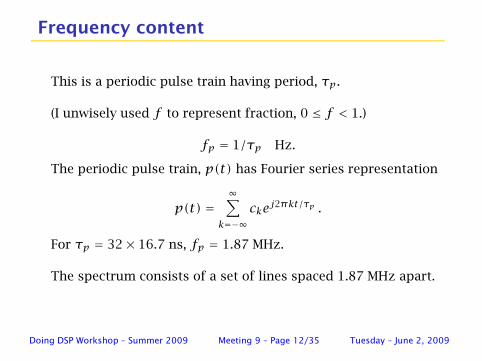
Frequency content
This is a periodic pulse train having period, τp.
(I unwisely used f to represent fraction, 0 ≤ f < 1.)
fp = 1/τp Hz.
The periodic pulse train, p(t) has Fourier series representation
p(t) =
∞∑
k=−∞
ckej2πkt/τp .
For τp = 32× 16.7 ns, fp = 1.87 MHz.
The spectrum consists of a set of lines spaced 1.87 MHz apart.
Doing DSP Workshop – Summer 2009 Meeting 9 – Page 12/35 Tuesday – June 2, 2009
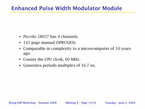
Enhanced Pulse Width Modulator Module
◮ Piccolo 28027 has 4 channels.
◮ 145 page manual (SPRUGE9).
◮ Comparable in complexity to a microcomputer of 10 years
ago.
◮ Counts the CPU clcok, 60 MHz.
◮ Generates periods multiples of 16.7 ns.
Doing DSP Workshop – Summer 2009 Meeting 9 – Page 13/35 Tuesday – June 2, 2009

Basic ePWM module
TZ1 TZ3to
CLOCKFAIL
EMUSTOP
EPWM1ENCLK
TBCLKSYNC
EPWM1SYNCI
EPWM1 Module
TZ5
TZ6
EPWM1SYNCO
EPWM1TZINT
EPWM1INT
EPWM2TZINT
EPWM2INT
EPWMxTZINT
EPWMxINT
PIE
EPWM2SYNCI
EPWM2 Module
TZ5
TZ6
EPWM2SYNCO
EPWM1SYNCO
EPWM1B
EPWM2B
TZ1 TZ3to
CLOCKFAIL
EMUSTOP
EPWM2ENCLK
TBCLKSYNC
EPWMxSYNCI
EPWMx Module
TZ5
TZ6
EPWMxB
CLOCKFAIL
EMUSTOPSystem Control
C28x CPUEPWMxENCLK
TBCLKSYNC
COMPOUT1COMPOUT2COMPOUT3
COMP
EPWM1SOCA
EPWM1SOCB
EPWM2SOCA
EPWM2SOCB
EPWMxSOCA
EPWMxSOCB
ADC
HR
PW
M
EPWM1A
EPWM2A
EPWMxA
eCAP1
EPWM1SOCA
EPWM2SOCA
EPWMxSOCA
EPWM1SOCB
EPWM2SOCB
EPWMxSOCB
ADCSOCAO
ADCSOCBO
EPWMSYNCI
GP
IO M
ux
Figure 1-1. Multiple ePWM Modules
Doing DSP Workshop – Summer 2009 Meeting 9 – Page 14/35 Tuesday – June 2, 2009

ePWM subsystems
EPWMxINT
EPWMxTZINT
EPWMxSOCA
EPWMxSOCB
EPWMxSYNCI
EPWMxSYNCOTime-base (TB) module
Counter-compare (CC) module
Action-qualifier (AQ) module
Dead-band (DB) module
PWM-chopper (PC) module
Event-trigger (ET) module
Trip-zone (TZ) modulePeripheral bus
ePWM module
TZ1 TZ3to
EPWMxA
EPWMxB
PIE
ADC
GPIOMUX
COMPxOUTCOMP
Digital Compare (DC) module
EQEP1ERR
CLOCKFAIL
EMUSTOP
Figure 1-2. Submodules and Signal Connections for an ePWM Module
Doing DSP Workshop – Summer 2009 Meeting 9 – Page 15/35 Tuesday – June 2, 2009
High Resolution PWM
◮ An enhancement to the ePWM.
◮ Extends the time resolution.
◮ Nominally divides 16.67 ns clock cycle into 111
subintervals of 150 ps.
◮ In effect, increases the interval resolution by almost 7 bits.
◮ Temperature calibration capability provided.
◮ Each 28027 ePWM channel has this enhancement.
◮ 36 page manual, SPRUGE8.
Doing DSP Workshop – Summer 2009 Meeting 9 – Page 16/35 Tuesday – June 2, 2009
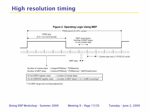
High resolution timing
(1 SYSCLK cycle)
Figure 2. Operating Logic Using MEP
Doing DSP Workshop – Summer 2009 Meeting 9 – Page 17/35 Tuesday – June 2, 2009

Setting the integer width
Integer part: Multiply the period in counts by value in the range
[0,1).
Samples are 12bits and are in the low 12bits of a 16bit word.
These are in simple binary form. (0V input maps to 0 and Vccmaps to 4095). Can model as being Q12.
The integer width count is the period count times the sample
value with the result right shifted 12 places. (Probably need to
use a long for the product.)
If the period count is a power of 2, say a count of 32 giving a
power of 5, then simply arithmetic shift the sample value by 7
bits.
Doing DSP Workshop – Summer 2009 Meeting 9 – Page 18/35 Tuesday – June 2, 2009

Setting the fractional width
Using the 12bit sample and period count of 32.
We need to multiply the high resolution step count. The
hardware can be used to determine this. It is sensitive to
temperature and voltage. A reasonable guess value is 111.
Having the period count times the sample value. Mask off the
top 9 bits keeping the low 7 bits. This is the fractional part in
Q7. Multiply by 111. Shift right by 7. This is the fractional count
part for setting high resolution.
I think this is correct. Actual code will differ because of how the
bits are arranged in the control words. Look before you leap.
Doing DSP Workshop – Summer 2009 Meeting 9 – Page 19/35 Tuesday – June 2, 2009

The controlSTICK RC filter
R = 470 Ohms, C = 10 nF. RC = 4.7× 10⁻⁶.
f3dB =1
2πRC= 33.9 kHz.
102
103
104
105
106
107
-50
-40
-30
-20
-10
0
Gain
(d
B)
Frequency (Hz)
controlSTICK RC lowpass filter response
Doing DSP Workshop – Summer 2009 Meeting 9 – Page 20/35 Tuesday – June 2, 2009

Modeling the ripple
Vcc
R
C 0
R
C
va
vb
vcc
GND
fτp (1− f)τp
time
0 ≤ f < 1
Doing DSP Workshop – Summer 2009 Meeting 9 – Page 21/35 Tuesday – June 2, 2009

Writing the equations
Assuming steady state. Want to determine va and vb as a
function of the fractional value f where 0 ≤ f < 1. Because our
introductory circuits course far in the distant past we can
immediately write
vb = va + (vcc − va)(1− e−fτp/τRC),
va = vbe(1−f )τp/τRC .
where τRC = RC. Solving for va gives
va = vccefτp/τRC
1− e−fτp/τRC
eτp/τRC − 1.
The equation for vb follows readily. The plots on the following
page were made using MATLAB.
Doing DSP Workshop – Summer 2009 Meeting 9 – Page 22/35 Tuesday – June 2, 2009

Ripple level plots
0 0.2 0.4 0.6 0.8 10
1
2
3
4
Va (
Volt
s)
Duty cycle fraction
0 0.2 0.4 0.6 0.8 10
0.02
0.04
0.06
0.08
0.1
Peak-t
o-p
eak r
ipp
le (
Volt
s)
Duty cycle fraction
Doing DSP Workshop – Summer 2009 Meeting 9 – Page 23/35 Tuesday – June 2, 2009

Some numbers
The RC values corresponded to those used on the controlSTICK.
◮ τp = 32/60E6, i.e., 32 controlSTICK clock tics.
◮ The supply, vcc was set to 3.3 Volts.
◮ The maximum peaktopeak ripple is 0.0936 Volts.
◮ The gain at frequency 1/τp is 0.0181.
◮ The peaktopeak amplitude of the fundamental at the RC output
is 0.076 Volts for f = 1/2.
Doing DSP Workshop – Summer 2009 Meeting 9 – Page 24/35 Tuesday – June 2, 2009

A better filter
Might try one more RC stage.
Use active filter built using an opamp.
What opamp, what filter topology, what parameters?
Doing DSP Workshop – Summer 2009 Meeting 9 – Page 25/35 Tuesday – June 2, 2009

TI OPA340 op-amps
Railtorail input
Railto rail output
Gain bandwidth: 5.5 MHz
Slew rate: 6V/µs
VS = 2.7V to 5V
OPEN-LOOP GAIN/PHASE vs FREQUENCY
0.1 1
160
140
120
100
80
60
40
20
0
–20V
olta
ge G
ain
(dB
)
0
–45
–90
–135
–180
Pha
se (
°)
Frequency (Hz)
10 100 1k 10k 100k 1M 10M
Available in 8pin DIP package. The OPA2340 costs $2.03 quantity 25.
Doing DSP Workshop – Summer 2009 Meeting 9 – Page 26/35 Tuesday – June 2, 2009

TI OPA350 op-amps
Railtorail input
Railto rail output
Gain bandwidth: 38 MHz
Slew rate: 22V/µs
VS = 2.7V to 5.5V
0.1 1
160
140
120
100
80
60
40
20
0
0
−45
−90
−135
−180
Pha
se( �
)
Frequency (Hz)10 100 1k 10k 100k 1M 10M 100M
G
φ
OPEN-LOOP GAIN/PHASE vs FREQUENCY
Vol
tage
Gai
n (d
B)
Available in 8pin DIP package. The OPA2350 costs $2.64 quantity 25.
Doing DSP Workshop – Summer 2009 Meeting 9 – Page 27/35 Tuesday – June 2, 2009
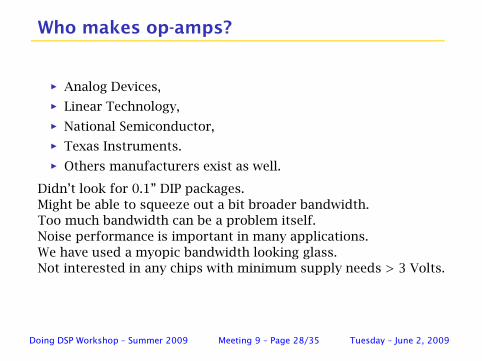
Who makes op-amps?
◮ Analog Devices,
◮ Linear Technology,
◮ National Semiconductor,
◮ Texas Instruments.
◮ Others manufacturers exist as well.
Didn’t look for 0.1” DIP packages.
Might be able to squeeze out a bit broader bandwidth.
Too much bandwidth can be a problem itself.
Noise performance is important in many applications.
We have used a myopic bandwidth looking glass.
Not interested in any chips with minimum supply needs > 3 Volts.
Doing DSP Workshop – Summer 2009 Meeting 9 – Page 28/35 Tuesday – June 2, 2009

Those holey white blocks
Hole mount parts are vanishing . . . adapt the surface mount parts!
Spark Fun $1.95.
Needs pin strips.
Or, you can adapt your approach!
Doing DSP Workshop – Summer 2009 Meeting 9 – Page 29/35 Tuesday – June 2, 2009

Dead bugs on perf board
Doing DSP Workshop – Summer 2009 Meeting 9 – Page 30/35 Tuesday – June 2, 2009

Need a steady hand — 0.05" spacing
Doing DSP Workshop – Summer 2009 Meeting 9 – Page 31/35 Tuesday – June 2, 2009

Power supply bypass capacitors
◮ Absolutely essential.
◮ Charge reserve used by switching devices.
◮ Prevents (generally) analog amplifiers from oscillating.
◮ Place as close to the supply pins as possible.
◮ Use 0.01 µF minimum. I always use 0.1 µF.
◮ Also 0.1 µF bypass any bulk supply storage electrolytics!!!!
When is a capacitor not a capacitor? When it’s an electrolytic.
◮ Place as early as possible when laying out PWB board!!!!
◮ Do not place ground planes under amplifier summing
junctions!!!
Doing DSP Workshop – Summer 2009 Meeting 9 – Page 32/35 Tuesday – June 2, 2009

Single-supply Sallen-Key filter?
TI offers assistance:
www-k.ext.ti.com/SRVS/Data/ti/KnowledgeBases/analog/document/faqs/ssexpert.htm .
Twopole, “low pass”, SallenKey filter:
Circuit from the TI single supply expert.
Doing DSP Workshop – Summer 2009 Meeting 9 – Page 33/35 Tuesday – June 2, 2009

More Sallen-Key arrangements
Vcc/2
R1
Vout
-
+
+Vcc
+Vcc
C1
Vin
Vin
Unity Gain Butterworth
Fo = 1/(2pRC)R1 = 0.47RR2 = 2.1RC1 = C2 = C3 = C
C1
Cin
Vcc/2
Vout
R3
+Vcc
Vout
Unity Gain Butterworth
Fo = 1/(2pRC)R1 = R2 = R/Ö2R3 = R/(2Ö2)C1 = CC2 = 4C
HIGH PASS
C2
R3
-
+
Gain = 2.3 dB
Fo = 1/(2.32pRC)R1 = 10RR2 = 0.001RR3 = 100RC1 = 10CC2 = C
Vcc/2
C1
Vin
BAND PASS
R2
R2
-
+
Cin
R1
C2
R1
C2
LOW PASS
R2
C3
From TI’s collection, SLOA058. Available on handouts page.
Doing DSP Workshop – Summer 2009 Meeting 9 – Page 34/35 Tuesday – June 2, 2009

Delta Sigma modulator DAC
a.k.a pulse density modulation DAC.
Doing DSP Workshop – Summer 2009 Meeting 9 – Page 35/35 Tuesday – June 2, 2009