Embed Size (px)
Citation preview
This is information on a product in full production.
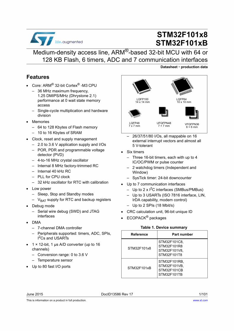
June 2015 DocID13586 Rev 17 1/101
STM32F101x8 STM32F101xB
Medium-density access line, ARM®-based 32-bit MCU with 64 or 128 KB Flash, 6 timers, ADC and 7 communication interfaces
Datasheet - production data
Features
Core: ARM® 32-bit Cortex® -M3 CPU
– 36 MHz maximum frequency,1.25 DMIPS/MHz (Dhrystone 2.1) performance at 0 wait state memory access
– Single-cycle multiplication and hardware division
Memories
– 64 to 128 Kbytes of Flash memory
– 10 to 16 Kbytes of SRAM
Clock, reset and supply management
– 2.0 to 3.6 V application supply and I/Os
– POR, PDR and programmable voltage detector (PVD)
– 4-to-16 MHz crystal oscillator
– Internal 8 MHz factory-trimmed RC
– Internal 40 kHz RC
– PLL for CPU clock
– 32 kHz oscillator for RTC with calibration
Low power
– Sleep, Stop and Standby modes
– VBAT supply for RTC and backup registers
Debug mode
– Serial wire debug (SWD) and JTAG interfaces
DMA
– 7-channel DMA controller
– Peripherals supported: timers, ADC, SPIs, I2Cs and USARTs
1 × 12-bit, 1 µs A/D converter (up to 16 channels)
– Conversion range: 0 to 3.6 V
– Temperature sensor
Up to 80 fast I/O ports
– 26/37/51/80 I/Os, all mappable on 16 external interrupt vectors and almost all 5 V-tolerant
Six timers
– Three 16-bit timers, each with up to 4 IC/OC/PWM or pulse counter
– 2 watchdog timers (Independent and Window)
– SysTick timer: 24-bit downcounter
Up to 7 communication interfaces
– Up to 2 x I2C interfaces (SMBus/PMBus)
– Up to 3 USARTs (ISO 7816 interface, LIN, IrDA capability, modem control)
– Up to 2 SPIs (18 Mbit/s)
CRC calculation unit, 96-bit unique ID
ECOPACK® packages
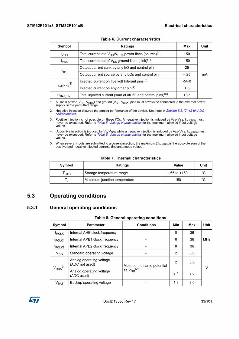
Table 1. Device summary
Reference Part number
STM32F101x8
STM32F101C8, STM32F101R8 STM32F101V8, STM32F101T8
STM32F101xB
STM32F101RB, STM32F101VB, STM32F101CBSTM32F101TB
LQFP487 x 7 mm
LQFP10014 x 14 mm
LQFP6410 x 10 mm
VFQFPN366 × 6 mm
UFQFPN487 × 7 mm
www.st.com
Contents STM32F101x8, STM32F101xB
2/101 DocID13586 Rev 17
Contents
1 Introduction . . . . . . . . . . . . . . . . . . . . . . . . . . . . . . . . . . . . . . . . . . . . . . . . 9
2 Description . . . . . . . . . . . . . . . . . . . . . . . . . . . . . . . . . . . . . . . . . . . . . . . . 10
2.1 Device overview . . . . . . . . . . . . . . . . . . . . . . . . . . . . . . . . . . . . . . . . . . . . .11
2.2 Full compatibility throughout the family . . . . . . . . . . . . . . . . . . . . . . . . . . 14
2.3 Overview . . . . . . . . . . . . . . . . . . . . . . . . . . . . . . . . . . . . . . . . . . . . . . . . . 15
2.3.1 ARM® Cortex® -M3 core with embedded Flash and SRAM . . . . . . . . . 15
2.3.2 Embedded Flash memory . . . . . . . . . . . . . . . . . . . . . . . . . . . . . . . . . . . 15
2.3.3 CRC (cyclic redundancy check) calculation unit . . . . . . . . . . . . . . . . . . 15
2.3.4 Embedded SRAM . . . . . . . . . . . . . . . . . . . . . . . . . . . . . . . . . . . . . . . . . 15
2.3.5 Nested vectored interrupt controller (NVIC) . . . . . . . . . . . . . . . . . . . . . . 15
2.3.6 External interrupt/event controller (EXTI) . . . . . . . . . . . . . . . . . . . . . . . 16
2.3.7 Clocks and startup . . . . . . . . . . . . . . . . . . . . . . . . . . . . . . . . . . . . . . . . . 16
2.3.8 Boot modes . . . . . . . . . . . . . . . . . . . . . . . . . . . . . . . . . . . . . . . . . . . . . . 16
2.3.9 Power supply schemes . . . . . . . . . . . . . . . . . . . . . . . . . . . . . . . . . . . . . 16
2.3.10 Power supply supervisor . . . . . . . . . . . . . . . . . . . . . . . . . . . . . . . . . . . . 16
2.3.11 Voltage regulator . . . . . . . . . . . . . . . . . . . . . . . . . . . . . . . . . . . . . . . . . . 17
2.3.12 Low-power modes . . . . . . . . . . . . . . . . . . . . . . . . . . . . . . . . . . . . . . . . . 17
2.3.13 DMA . . . . . . . . . . . . . . . . . . . . . . . . . . . . . . . . . . . . . . . . . . . . . . . . . . . . 18
2.3.14 RTC (real-time clock) and backup registers . . . . . . . . . . . . . . . . . . . . . . 18
2.3.15 Independent watchdog . . . . . . . . . . . . . . . . . . . . . . . . . . . . . . . . . . . . . 18
2.3.16 Window watchdog . . . . . . . . . . . . . . . . . . . . . . . . . . . . . . . . . . . . . . . . . 18
2.3.17 SysTick timer . . . . . . . . . . . . . . . . . . . . . . . . . . . . . . . . . . . . . . . . . . . . . 19
2.3.18 General-purpose timers (TIMx) . . . . . . . . . . . . . . . . . . . . . . . . . . . . . . . 19
2.3.19 I²C bus . . . . . . . . . . . . . . . . . . . . . . . . . . . . . . . . . . . . . . . . . . . . . . . . . . 19
2.3.20 Universal synchronous/asynchronous receiver transmitter (USART) . . 19
2.3.21 Serial peripheral interface (SPI) . . . . . . . . . . . . . . . . . . . . . . . . . . . . . . . 19
2.3.22 GPIOs (general-purpose inputs/outputs) . . . . . . . . . . . . . . . . . . . . . . . . 19
2.3.23 ADC (analog to digital converter) . . . . . . . . . . . . . . . . . . . . . . . . . . . . . . 20
2.3.24 Temperature sensor . . . . . . . . . . . . . . . . . . . . . . . . . . . . . . . . . . . . . . . . 20
2.3.25 Serial wire JTAG debug port (SWJ-DP) . . . . . . . . . . . . . . . . . . . . . . . . . 20
3 Pinouts and pin description . . . . . . . . . . . . . . . . . . . . . . . . . . . . . . . . . . 21

DocID13586 Rev 17 3/101
STM32F101x8, STM32F101xB Contents
4
4 Memory mapping . . . . . . . . . . . . . . . . . . . . . . . . . . . . . . . . . . . . . . . . . . . 29
5 Electrical characteristics . . . . . . . . . . . . . . . . . . . . . . . . . . . . . . . . . . . . 30
5.1 Parameter conditions . . . . . . . . . . . . . . . . . . . . . . . . . . . . . . . . . . . . . . . . 30
5.1.1 Minimum and maximum values . . . . . . . . . . . . . . . . . . . . . . . . . . . . . . . 30
5.1.2 Typical values . . . . . . . . . . . . . . . . . . . . . . . . . . . . . . . . . . . . . . . . . . . . 30
5.1.3 Typical curves . . . . . . . . . . . . . . . . . . . . . . . . . . . . . . . . . . . . . . . . . . . . 30
5.1.4 Loading capacitor . . . . . . . . . . . . . . . . . . . . . . . . . . . . . . . . . . . . . . . . . 30
5.1.5 Pin input voltage . . . . . . . . . . . . . . . . . . . . . . . . . . . . . . . . . . . . . . . . . . 30
5.1.6 Power supply scheme . . . . . . . . . . . . . . . . . . . . . . . . . . . . . . . . . . . . . . 31
5.1.7 Current consumption measurement . . . . . . . . . . . . . . . . . . . . . . . . . . . 32
5.2 Absolute maximum ratings . . . . . . . . . . . . . . . . . . . . . . . . . . . . . . . . . . . . 32
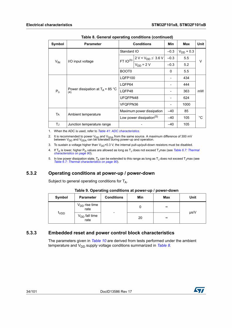
5.3 Operating conditions . . . . . . . . . . . . . . . . . . . . . . . . . . . . . . . . . . . . . . . . 33
5.3.1 General operating conditions . . . . . . . . . . . . . . . . . . . . . . . . . . . . . . . . . 33
5.3.2 Operating conditions at power-up / power-down . . . . . . . . . . . . . . . . . . 34
5.3.3 Embedded reset and power control block characteristics . . . . . . . . . . . 34
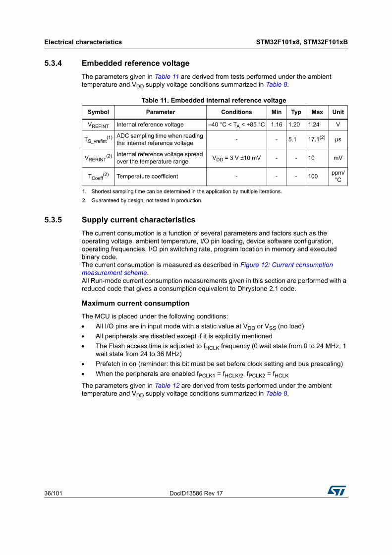
5.3.4 Embedded reference voltage . . . . . . . . . . . . . . . . . . . . . . . . . . . . . . . . . 36
5.3.5 Supply current characteristics . . . . . . . . . . . . . . . . . . . . . . . . . . . . . . . . 36
5.3.6 External clock source characteristics . . . . . . . . . . . . . . . . . . . . . . . . . . . 44
5.3.7 Internal clock source characteristics . . . . . . . . . . . . . . . . . . . . . . . . . . . 49
5.3.8 PLL characteristics . . . . . . . . . . . . . . . . . . . . . . . . . . . . . . . . . . . . . . . . 50
5.3.9 Memory characteristics . . . . . . . . . . . . . . . . . . . . . . . . . . . . . . . . . . . . . 51
5.3.10 EMC characteristics . . . . . . . . . . . . . . . . . . . . . . . . . . . . . . . . . . . . . . . . 51
5.3.11 Absolute maximum ratings (electrical sensitivity) . . . . . . . . . . . . . . . . . 53
5.3.12 I/O current injection characteristics . . . . . . . . . . . . . . . . . . . . . . . . . . . . 53
5.3.13 I/O port characteristics . . . . . . . . . . . . . . . . . . . . . . . . . . . . . . . . . . . . . . 55
5.3.14 NRST pin characteristics . . . . . . . . . . . . . . . . . . . . . . . . . . . . . . . . . . . . 60
5.3.15 TIM timer characteristics . . . . . . . . . . . . . . . . . . . . . . . . . . . . . . . . . . . . 62
5.3.16 Communications interfaces . . . . . . . . . . . . . . . . . . . . . . . . . . . . . . . . . . 62
5.3.17 12-bit ADC characteristics . . . . . . . . . . . . . . . . . . . . . . . . . . . . . . . . . . . 68
5.3.18 Temperature sensor characteristics . . . . . . . . . . . . . . . . . . . . . . . . . . . . 72
6 Package characteristics . . . . . . . . . . . . . . . . . . . . . . . . . . . . . . . . . . . . . 73
6.1 Package mechanical data . . . . . . . . . . . . . . . . . . . . . . . . . . . . . . . . . . . . 73
6.2 UFQFPN48 package information . . . . . . . . . . . . . . . . . . . . . . . . . . . . . . . 73
6.3 VFQFPN36 package information . . . . . . . . . . . . . . . . . . . . . . . . . . . . . . . 76
Contents STM32F101x8, STM32F101xB
4/101 DocID13586 Rev 17
6.4 LQFP100 package information . . . . . . . . . . . . . . . . . . . . . . . . . . . . . . . . . 80
6.5 LQFP64 package information . . . . . . . . . . . . . . . . . . . . . . . . . . . . . . . . . . 83
6.6 LQFP48 package information . . . . . . . . . . . . . . . . . . . . . . . . . . . . . . . . . . 86
6.7 Thermal characteristics . . . . . . . . . . . . . . . . . . . . . . . . . . . . . . . . . . . . . . 90
6.7.1 Reference document . . . . . . . . . . . . . . . . . . . . . . . . . . . . . . . . . . . . . . . 90
6.7.2 Evaluating the maximum junction temperature for an application . . . . . 91
7 Ordering information scheme . . . . . . . . . . . . . . . . . . . . . . . . . . . . . . . . 92
8 Revision history . . . . . . . . . . . . . . . . . . . . . . . . . . . . . . . . . . . . . . . . . . . 94
DocID13586 Rev 17 5/101
STM32F101x8, STM32F101xB List of Tables
6
List of Tables
Table 1. Device summary . . . . . . . . . . . . . . . . . . . . . . . . . . . . . . . . . . . . . . . . . . . . . . . . . . . . . . . . . . 1Table 2. Device features and peripheral counts (STM32F101xx
medium-density access line) . . . . . . . . . . . . . . . . . . . . . . . . . . . . . . . . . . . . . . . . . . . . . . . 11Table 3. STM32F101xx family . . . . . . . . . . . . . . . . . . . . . . . . . . . . . . . . . . . . . . . . . . . . . . . . . . . . . 14Table 4. Medium-density STM32F101xx pin definitions . . . . . . . . . . . . . . . . . . . . . . . . . . . . . . . . . . 24Table 5. Voltage characteristics . . . . . . . . . . . . . . . . . . . . . . . . . . . . . . . . . . . . . . . . . . . . . . . . . . . . 32Table 6. Current characteristics . . . . . . . . . . . . . . . . . . . . . . . . . . . . . . . . . . . . . . . . . . . . . . . . . . . . 33Table 7. Thermal characteristics. . . . . . . . . . . . . . . . . . . . . . . . . . . . . . . . . . . . . . . . . . . . . . . . . . . . 33Table 8. General operating conditions . . . . . . . . . . . . . . . . . . . . . . . . . . . . . . . . . . . . . . . . . . . . . . . 33Table 9. Operating conditions at power-up / power-down . . . . . . . . . . . . . . . . . . . . . . . . . . . . . . . . 34Table 10. Embedded reset and power control block characteristics. . . . . . . . . . . . . . . . . . . . . . . . . . 35Table 11. Embedded internal reference voltage. . . . . . . . . . . . . . . . . . . . . . . . . . . . . . . . . . . . . . . . . 36Table 12. Maximum current consumption in Run mode, code with data processing
running from Flash . . . . . . . . . . . . . . . . . . . . . . . . . . . . . . . . . . . . . . . . . . . . . . . . . . . . . . . 37Table 13. Maximum current consumption in Run mode, code with data processing
running from RAM. . . . . . . . . . . . . . . . . . . . . . . . . . . . . . . . . . . . . . . . . . . . . . . . . . . . . . . . 37Table 14. Maximum current consumption in Sleep mode, code running from Flash
or RAM . . . . . . . . . . . . . . . . . . . . . . . . . . . . . . . . . . . . . . . . . . . . . . . . . . . . . . . . . . . . . . . . 39Table 15. Typical and maximum current consumptions in Stop and Standby modes . . . . . . . . . . . . 39Table 16. Typical current consumption in Run mode, code with data processing
running from Flash . . . . . . . . . . . . . . . . . . . . . . . . . . . . . . . . . . . . . . . . . . . . . . . . . . . . . . . 42Table 17. Typical current consumption in Sleep mode, code running from Flash or RAM. . . . . . . . . 43Table 18. Peripheral current consumption . . . . . . . . . . . . . . . . . . . . . . . . . . . . . . . . . . . . . . . . . . . . . 44Table 19. High-speed external user clock characteristics. . . . . . . . . . . . . . . . . . . . . . . . . . . . . . . . . . 45Table 20. Low-speed external user clock characteristics . . . . . . . . . . . . . . . . . . . . . . . . . . . . . . . . . . 45Table 21. HSE 4-16 MHz oscillator characteristics. . . . . . . . . . . . . . . . . . . . . . . . . . . . . . . . . . . . . . . 47Table 22. LSE oscillator characteristics (fLSE = 32.768 kHz) . . . . . . . . . . . . . . . . . . . . . . . . . . . . . . . 48Table 23. HSI oscillator characteristics. . . . . . . . . . . . . . . . . . . . . . . . . . . . . . . . . . . . . . . . . . . . . . . . 49Table 24. LSI oscillator characteristics . . . . . . . . . . . . . . . . . . . . . . . . . . . . . . . . . . . . . . . . . . . . . . . 50Table 25. Low-power mode wakeup timings . . . . . . . . . . . . . . . . . . . . . . . . . . . . . . . . . . . . . . . . . . . 50Table 26. PLL characteristics . . . . . . . . . . . . . . . . . . . . . . . . . . . . . . . . . . . . . . . . . . . . . . . . . . . . . . . 50Table 27. Flash memory characteristics . . . . . . . . . . . . . . . . . . . . . . . . . . . . . . . . . . . . . . . . . . . . . . . 51Table 28. EMS characteristics . . . . . . . . . . . . . . . . . . . . . . . . . . . . . . . . . . . . . . . . . . . . . . . . . . . . . . 52Table 29. EMI characteristics . . . . . . . . . . . . . . . . . . . . . . . . . . . . . . . . . . . . . . . . . . . . . . . . . . . . . . . 52Table 30. ESD absolute maximum ratings . . . . . . . . . . . . . . . . . . . . . . . . . . . . . . . . . . . . . . . . . . . . . 53Table 31. Electrical sensitivities . . . . . . . . . . . . . . . . . . . . . . . . . . . . . . . . . . . . . . . . . . . . . . . . . . . . . 53Table 32. I/O current injection susceptibility . . . . . . . . . . . . . . . . . . . . . . . . . . . . . . . . . . . . . . . . . . . . 54Table 33. I/O static characteristics . . . . . . . . . . . . . . . . . . . . . . . . . . . . . . . . . . . . . . . . . . . . . . . . . . . 55Table 34. Output voltage characteristics . . . . . . . . . . . . . . . . . . . . . . . . . . . . . . . . . . . . . . . . . . . . . . 58Table 35. I/O AC characteristics . . . . . . . . . . . . . . . . . . . . . . . . . . . . . . . . . . . . . . . . . . . . . . . . . . . . . 59Table 36. NRST pin characteristics . . . . . . . . . . . . . . . . . . . . . . . . . . . . . . . . . . . . . . . . . . . . . . . . . . 60Table 37. TIMx characteristics . . . . . . . . . . . . . . . . . . . . . . . . . . . . . . . . . . . . . . . . . . . . . . . . . . . . . . 62Table 38. I2C characteristics. . . . . . . . . . . . . . . . . . . . . . . . . . . . . . . . . . . . . . . . . . . . . . . . . . . . . . . . 63Table 39. SCL frequency (fPCLK1= 36 MHz, VDD_I2C = 3.3 V) . . . . . . . . . . . . . . . . . . . . . . . . . . . . . . 64Table 40. SPI characteristics . . . . . . . . . . . . . . . . . . . . . . . . . . . . . . . . . . . . . . . . . . . . . . . . . . . . . . . 65Table 41. ADC characteristics . . . . . . . . . . . . . . . . . . . . . . . . . . . . . . . . . . . . . . . . . . . . . . . . . . . . . . 68Table 42. RAIN max for fADC = 14 MHz. . . . . . . . . . . . . . . . . . . . . . . . . . . . . . . . . . . . . . . . . . . . . . . . 69Table 43. ADC accuracy - limited test conditions . . . . . . . . . . . . . . . . . . . . . . . . . . . . . . . . . . . . . . . 69
List of Tables STM32F101x8, STM32F101xB
6/101 DocID13586 Rev 17
Table 44. ADC accuracy . . . . . . . . . . . . . . . . . . . . . . . . . . . . . . . . . . . . . . . . . . . . . . . . . . . . . . . . . . 70Table 45. TS characteristics . . . . . . . . . . . . . . . . . . . . . . . . . . . . . . . . . . . . . . . . . . . . . . . . . . . . . . . . 72Table 46. UFQFPN48 - 48-lead, 7x7 mm, 0.5 mm pitch, ultra thin fine pitch quad flat
package mechanical data . . . . . . . . . . . . . . . . . . . . . . . . . . . . . . . . . . . . . . . . . . . . . . . . . . 74Table 47. VFQFPN36 - 36-pin, 6x6 mm, 0.5 mm pitch very thin profile fine pitch quad flat
package mechanical data . . . . . . . . . . . . . . . . . . . . . . . . . . . . . . . . . . . . . . . . . . . . . . . . . . 77Table 48. LQPF100 - 100-pin, 14 x 14 mm low-profile quad flat package
mechanical data . . . . . . . . . . . . . . . . . . . . . . . . . . . . . . . . . . . . . . . . . . . . . . . . . . . . . . . . . 80Table 49. LQFP64 - 64-pin, 10 x 10 mm low-profile quad flat
package mechanical data . . . . . . . . . . . . . . . . . . . . . . . . . . . . . . . . . . . . . . . . . . . . . . . . . . 83Table 50. LQFP48 - 48-pin, 7 x 7 mm low-profile quad flat package
mechanical data . . . . . . . . . . . . . . . . . . . . . . . . . . . . . . . . . . . . . . . . . . . . . . . . . . . . . . . . . 87Table 51. Package thermal characteristics . . . . . . . . . . . . . . . . . . . . . . . . . . . . . . . . . . . . . . . . . . . . . 90Table 52. Ordering information scheme . . . . . . . . . . . . . . . . . . . . . . . . . . . . . . . . . . . . . . . . . . . . . . . 92Table 53. Document revision history . . . . . . . . . . . . . . . . . . . . . . . . . . . . . . . . . . . . . . . . . . . . . . . . . 94

DocID13586 Rev 17 7/101
STM32F101x8, STM32F101xB List of Figures
8
List of Figures
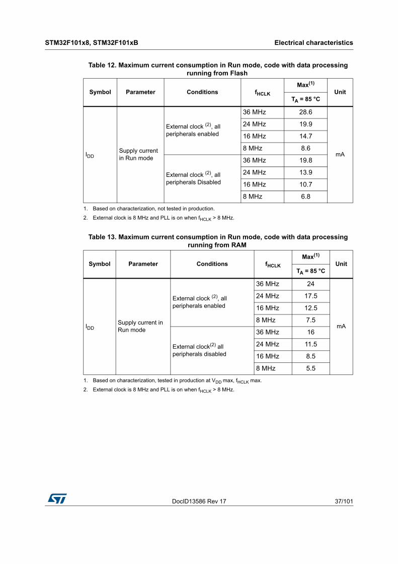
Figure 1. STM32F101xx medium-density access line block diagram . . . . . . . . . . . . . . . . . . . . . . . . 12Figure 2. Clock tree . . . . . . . . . . . . . . . . . . . . . . . . . . . . . . . . . . . . . . . . . . . . . . . . . . . . . . . . . . . . . . 13Figure 3. STM32F101xx medium-density access line LQFP100 pinout . . . . . . . . . . . . . . . . . . . . . . 21Figure 4. STM32F101xx medium-density access line LQFP64 pinout . . . . . . . . . . . . . . . . . . . . . . . 22Figure 5. STM32F101xx medium-density access line LQFP48 pinout . . . . . . . . . . . . . . . . . . . . . . . 22Figure 6. STM32F101xx medium-density access line UFQPFN48 pinout. . . . . . . . . . . . . . . . . . . . . 23Figure 7. STM32F101xx medium-density access line VFQPFN36 pinout . . . . . . . . . . . . . . . . . . . . . 23Figure 8. Memory map. . . . . . . . . . . . . . . . . . . . . . . . . . . . . . . . . . . . . . . . . . . . . . . . . . . . . . . . . . . . 29Figure 9. Pin loading conditions. . . . . . . . . . . . . . . . . . . . . . . . . . . . . . . . . . . . . . . . . . . . . . . . . . . . . 31Figure 10. Pin input voltage . . . . . . . . . . . . . . . . . . . . . . . . . . . . . . . . . . . . . . . . . . . . . . . . . . . . . . . . . 31Figure 11. Power supply scheme. . . . . . . . . . . . . . . . . . . . . . . . . . . . . . . . . . . . . . . . . . . . . . . . . . . . . 31Figure 12. Current consumption measurement scheme . . . . . . . . . . . . . . . . . . . . . . . . . . . . . . . . . . . 32Figure 13. Typical current consumption in Run mode versus frequency (at 3.6 V) -
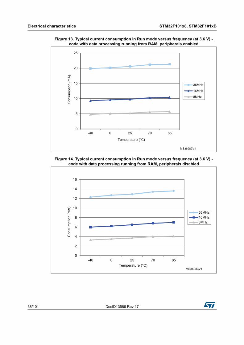
code with data processing running from RAM, peripherals enabled. . . . . . . . . . . . . . . . . . 38Figure 14. Typical current consumption in Run mode versus frequency (at 3.6 V) -
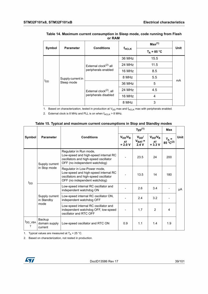
code with data processing running from RAM, peripherals disabled . . . . . . . . . . . . . . . . . 38Figure 15. Typical current consumption on VBAT with RTC on versus temperature at different
VBAT values . . . . . . . . . . . . . . . . . . . . . . . . . . . . . . . . . . . . . . . . . . . . . . . . . . . . . . . . . . . . 40Figure 16. Typical current consumption in Stop mode with regulator in Run mode versus
temperature at VDD = 3.3 V and 3.6 V . . . . . . . . . . . . . . . . . . . . . . . . . . . . . . . . . . . . . . . . 40Figure 17. Typical current consumption in Stop mode with regulator in Low-power mode versus
temperature at VDD = 3.3 V and 3.6 V . . . . . . . . . . . . . . . . . . . . . . . . . . . . . . . . . . . . . . . . 41Figure 18. Typical current consumption in Standby mode versus temperature at VDD = 3.3 V and
3.6 V . . . . . . . . . . . . . . . . . . . . . . . . . . . . . . . . . . . . . . . . . . . . . . . . . . . . . . . . . . . . . . . . . . 41Figure 19. High-speed external clock source AC timing diagram . . . . . . . . . . . . . . . . . . . . . . . . . . . . 46Figure 20. Low-speed external clock source AC timing diagram. . . . . . . . . . . . . . . . . . . . . . . . . . . . . 46Figure 21. Typical application with an 8 MHz crystal . . . . . . . . . . . . . . . . . . . . . . . . . . . . . . . . . . . . . . 47Figure 22. Typical application with a 32.768 kHz crystal . . . . . . . . . . . . . . . . . . . . . . . . . . . . . . . . . . . 49Figure 23. Standard I/O input characteristics - CMOS port . . . . . . . . . . . . . . . . . . . . . . . . . . . . . . . . . 56Figure 24. Standard I/O input characteristics - TTL port . . . . . . . . . . . . . . . . . . . . . . . . . . . . . . . . . . . 56Figure 25. 5 V tolerant I/O input characteristics - CMOS port . . . . . . . . . . . . . . . . . . . . . . . . . . . . . . . 57Figure 26. 5 V tolerant I/O input characteristics - TTL port . . . . . . . . . . . . . . . . . . . . . . . . . . . . . . . . . 57Figure 27. I/O AC characteristics definition . . . . . . . . . . . . . . . . . . . . . . . . . . . . . . . . . . . . . . . . . . . . . 60Figure 28. Recommended NRST pin protection . . . . . . . . . . . . . . . . . . . . . . . . . . . . . . . . . . . . . . . . . 61Figure 29. I2C bus AC waveforms and measurement circuit(1) . . . . . . . . . . . . . . . . . . . . . . . . . . . . . . 64Figure 30. SPI timing diagram - slave mode and CPHA = 0 . . . . . . . . . . . . . . . . . . . . . . . . . . . . . . . . 66Figure 31. SPI timing diagram - slave mode and CPHA = 1(1) . . . . . . . . . . . . . . . . . . . . . . . . . . . . . . 66Figure 32. SPI timing diagram - master mode(1) . . . . . . . . . . . . . . . . . . . . . . . . . . . . . . . . . . . . . . . . . 67Figure 33. ADC accuracy characteristics . . . . . . . . . . . . . . . . . . . . . . . . . . . . . . . . . . . . . . . . . . . . . . . 70Figure 34. Typical connection diagram using the ADC . . . . . . . . . . . . . . . . . . . . . . . . . . . . . . . . . . . . 71Figure 35. Power supply and reference decoupling (VREF+ not connected to VDDA). . . . . . . . . . . . . . 71Figure 36. Power supply and reference decoupling (VREF+ connected to VDDA). . . . . . . . . . . . . . . . . 72Figure 37. UFQFPN48 7 x 7 mm, 0.5 mm pitch, package outline . . . . . . . . . . . . . . . . . . . . . . . . . . . . 73Figure 38. UFQFPN48 recommended footprint . . . . . . . . . . . . . . . . . . . . . . . . . . . . . . . . . . . . . . . . . . 74Figure 39. UFQFPN48 marking example (package top view) . . . . . . . . . . . . . . . . . . . . . . . . . . . . . . . 75Figure 40. VFQFPN36 - 36-pin, 6x6 mm, 0.5 mm pitch very thin profile fine pitch quad flat
package outline. . . . . . . . . . . . . . . . . . . . . . . . . . . . . . . . . . . . . . . . . . . . . . . . . . . . . . . . . . 76Figure 41. VFQFPN36 - 36-pin, 6x6 mm, 0.5 mm pitch very thin profile fine pitch quad flat
List of Figures STM32F101x8, STM32F101xB
8/101 DocID13586 Rev 17
package recommended footprint . . . . . . . . . . . . . . . . . . . . . . . . . . . . . . . . . . . . . . . . . . . . 78Figure 42. VFQFPN36 marking example (package top view) . . . . . . . . . . . . . . . . . . . . . . . . . . . . . . . 79Figure 43. LQFP100 - 100-pin, 14 x 14 mm low-profile quad flat package outline . . . . . . . . . . . . . . . 80Figure 44. LQFP100 - 100-pin, 14 x 14 mm low-profile quad flat
recommended footprint . . . . . . . . . . . . . . . . . . . . . . . . . . . . . . . . . . . . . . . . . . . . . . . . . . . . 81Figure 45. LQFP100 marking example (package top view) . . . . . . . . . . . . . . . . . . . . . . . . . . . . . . . . . 82Figure 46. LQFP64 - 64-pin, 10 x 10 mm low-profile quad flat package outline . . . . . . . . . . . . . . . . . 83Figure 47. LQFP64 - 64-pin, 10 x 10 mm low-profile quad flat package
recommended footprint . . . . . . . . . . . . . . . . . . . . . . . . . . . . . . . . . . . . . . . . . . . . . . . . . . . . 84Figure 48. LQFP64 marking example (package top view) . . . . . . . . . . . . . . . . . . . . . . . . . . . . . . . . . . 85Figure 49. LQFP48 - 48-pin, 7 x 7 mm low-profile quad flat package outline . . . . . . . . . . . . . . . . . . . 86Figure 50. LQFP48 - 48-pin, 7 x 7 mm low-profile quad flat package
recommended footprint . . . . . . . . . . . . . . . . . . . . . . . . . . . . . . . . . . . . . . . . . . . . . . . . . . . . 88Figure 51. LQFP48 marking example (package top view) . . . . . . . . . . . . . . . . . . . . . . . . . . . . . . . . . . 89Figure 52. LQFP64 PD max vs. TA . . . . . . . . . . . . . . . . . . . . . . . . . . . . . . . . . . . . . . . . . . . . . . . . . . . 91
DocID13586 Rev 17 9/101
STM32F101x8, STM32F101xB Introduction
100
1 Introduction
This datasheet provides the ordering information and mechanical device characteristics of the STM32F101x8 and STM32F101xB medium-density access line microcontrollers. For more details on the whole STMicroelectronics STM32F101xx family, please refer to Section 2.2: Full compatibility throughout the family.
The medium-density STM32F101xx datasheet should be read in conjunction with the low-, medium- and high-density STM32F10xxx reference manual.For information on programming, erasing and protection of the internal Flash memory please refer to the STM32F10xxx Flash programming manual.The reference and Flash programming manuals are both available from the STMicroelectronics website www.st.com.
For information on the Cortex® -M3 core please refer to the Cortex® -M3 Technical Reference Manual, available from the www.arm.com website.
Description STM32F101x8, STM32F101xB
10/101 DocID13586 Rev 17
2 Description
The STM32F101xB and STM32F101x8 medium-density access line family incorporates the high-performance ARM® Cortex® -M3 32-bit RISC core operating at a 36 MHz frequency, high-speed embedded memories (Flash memory up to 128 Kbytes and SRAM up to 16 Kbytes), and an extensive range of enhanced peripherals and I/Os connected to two APB buses. All devices offer standard communication interfaces (two I2Cs, two SPIs, and up to three USARTs), one 12-bit ADC and three general-purpose 16-bit timers.
The STM32F101xx medium-density access line family operates in the –40 to +85 °C temperature range, from a 2.0 to 3.6 V power supply. A comprehensive set of power-saving mode allows the design of low-power applications.
The STM32F101xx medium-density access line family includes devices in four different packages ranging from 36 pins to 100 pins. Depending on the device chosen, different sets of peripherals are included, the description below gives an overview of the complete range of peripherals proposed in this family.
These features make the STM32F101xx medium-density access line microcontroller family suitable for a wide range of applications such as application control and user interface, medical and handheld equipment, PC peripherals, gaming and GPS platforms, industrial applications, PLCs, inverters, printers, scanners, alarm systems, Video intercoms, and HVACs.
DocID13586 Rev 17 11/101
STM32F101x8, STM32F101xB Description
100
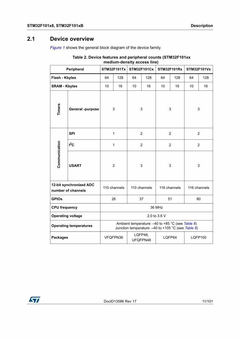
2.1 Device overview
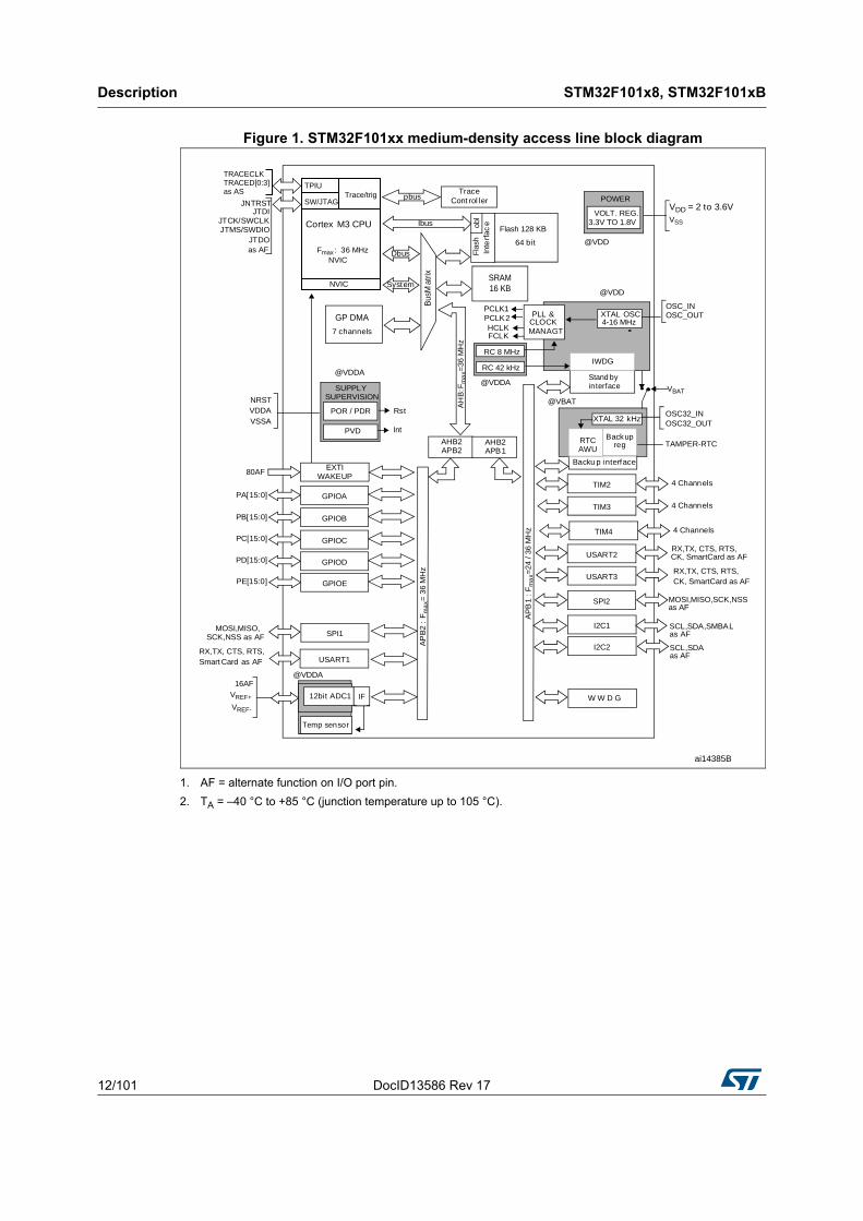
Figure 1 shows the general block diagram of the device family.
Table 2. Device features and peripheral counts (STM32F101xx medium-density access line)
Peripheral STM32F101Tx STM32F101Cx STM32F101Rx STM32F101Vx
Flash - Kbytes 64 128 64 128 64 128 64 128
SRAM - Kbytes 10 16 10 16 10 16 10 16
Tim
ers
General -purpose 3 3 3 3
Co
mm
un
icat
ion
SPI 1 2 2 2
I2C 1 2 2 2
USART 2 3 3 3
12-bit synchronized ADC
number of channels110 channels 110 channels 116 channels 116 channels
GPIOs 26 37 51 80
CPU frequency 36 MHz
Operating voltage 2.0 to 3.6 V
Operating temperaturesAmbient temperature: –40 to +85 °C (see Table 8)
Junction temperature: –40 to +105 °C (see Table 8)
Packages VFQFPN36LQFP48,
UFQFPN48LQFP64 LQFP100
Description STM32F101x8, STM32F101xB
12/101 DocID13586 Rev 17
Figure 1. STM32F101xx medium-density access line block diagram
1. AF = alternate function on I/O port pin.
2. TA = –40 °C to +85 °C (junction temperature up to 105 °C).
Temp sensor
PA[15:0]
EXTI
W W D G
NVIC
12bit ADC1
SWD
16AF
JTDIJTCK/SWCLKJTMS/SWDIO
JNTRST
JTDO
NRST
VDD = 2 to 3.6V
80AF
PB[15:0]
PC[15:0]
AHB2
MOSI,MISO,SCK,NSS
SRAM
2x(8x16bit)
WAKEUP
GPIOA
GPIOB
GPIOC
Fmax: 36 MHz
VSS
SCL,SDAI2C2
VREF+
GP DMA
TIM2
TIM3
XTAL OSC 4-16 MHz
XTAL 32 kHz
OSC_INOSC_OUT
OSC32_OUTOSC32_IN
PLL &
AP
B1
: F
ma
x=24
/ 36
MH
z
PCLK1
HCLKCLOCK MANAGT
PCLK2
as AF
as AF
VOLT. REG.3.3V TO 1.8V
POWER
Backu p interface
as AF
16 KB
RTC
RC 8 MHz
Cortex M3 CPU
USART1
USART2
SPI2
7 channels
Backupreg
SCL,SDA,SMBALI2C1as AF
RX,TX, CTS, RTS,USART3
VREF-
PD[15:0] GPIOD
AH
B:F
ma
x=36
MH
z
4 Channels
4 Channels
FCLK
RC 42 kHzStand by
IWDG
@VDD
@VBATPOR / PDR
SUPPLY
@VDDA
VDDAVSSA
@VDDA
VBAT
CK, SmartCard as AF
RX,TX, CTS, RTS,Smart Card as AF
RX,TX, CTS, RTS,
AP
B2
: F
ma
x= 3
6 M
Hz
NVIC
SPI1MOSI,MISO,
SCK,NSS as AF
IF
interface@VDDA
SUPERVISION
PVD
Rst
Int
@VDD
AHB2APB2 APB1 AWU
TAMPER-RTC
PE[15:0] GPIOE
Flash 128 KB
Bus
Mat
rix
64 bit
Inte
rfac
eIbus
Dbus
pbus
obl
Fla
sh
Trace Cont rol ler
System
TIM4 4 Channels
ai14385B
TRACECLKTRACED[0:3]as AS
SW/JTAG
TPIUTrace/trig
CK, SmartCard as AF
DocID13586 Rev 17 13/101
STM32F101x8, STM32F101xB Description
100
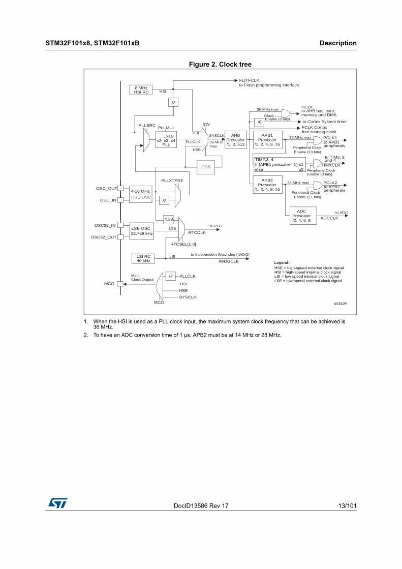
Figure 2. Clock tree
1. When the HSI is used as a PLL clock input, the maximum system clock frequency that can be achieved is 36 MHz.
2. To have an ADC conversion time of 1 µs, APB2 must be at 14 MHz or 28 MHz.
HSE OSC
4-16 MHz
OSC_IN
OSC_OUT
OSC32_IN
OSC32_OUT
LSE OSC32.768 kHz
HSI RC8 MHz
LSI RC40 kHz
to Independent Watchdog (IWDG)
PLLx2, x3, x4
PLLMUL
Legend:
MCO Clock OutputMain
PLLXTPRE
/2
..., x16 AHBPrescaler/1, 2..512
/2 PLLCLK
HSI
HSE
APB1Prescaler
/1, 2, 4, 8, 16
ADCPrescaler/2, 4, 6, 8
ADCCLK
PCLK1
HCLK
PLLCLK
to AHB bus, core, memory and DMA
to TIM2, 3and 4
to ADC
LSE
LSI
HSI
/128
/2
HSI
HSEperipheralsto APB1
Peripheral Clock Enable (13 bits)
Enable (3 bits)Peripheral Clock
APB2Prescaler
/1, 2, 4, 8, 16
PCLK2
peripheralsto APB2
Peripheral Clock Enable (11 bits)
36 MHz max
36 MHz max
to RTC
PLLSRC SW
MCO
CSS
to Cortex System timer/8
Clock Enable (3 bits)
SYSCLK
RTCCLK
RTCSEL[1:0]
TIMXCLK
IWDGCLK
SYSCLK
FCLK Cortexfree running clock
TIM2,3, 4If (APB1 prescaler =1) x1else x2
HSE = high-speed external clock signalHSI = high-speed internal clock signalLSI = low-speed internal clock signalLSE = low-speed external clock signal
ai15104
36 MHz max
36 MHzmax
FLITFCLKto Flash programming interface
Description STM32F101x8, STM32F101xB
14/101 DocID13586 Rev 17
2.2 Full compatibility throughout the family
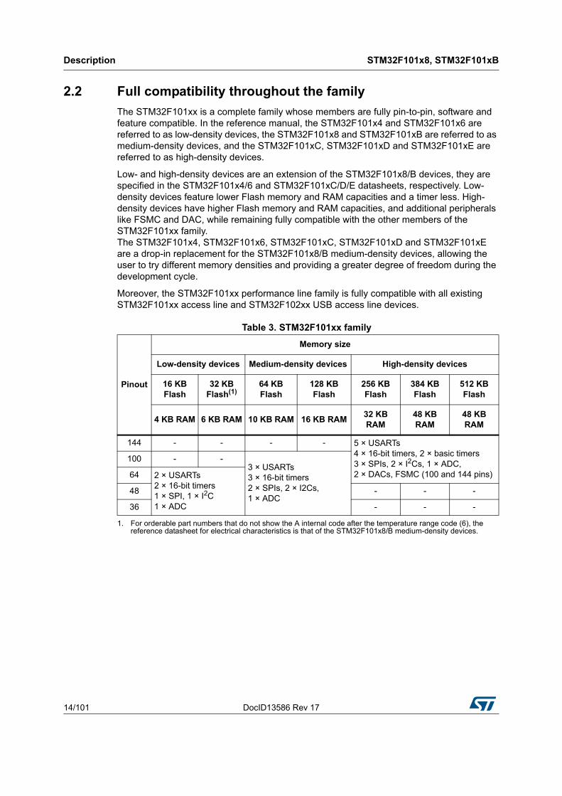
The STM32F101xx is a complete family whose members are fully pin-to-pin, software and feature compatible. In the reference manual, the STM32F101x4 and STM32F101x6 are referred to as low-density devices, the STM32F101x8 and STM32F101xB are referred to as medium-density devices, and the STM32F101xC, STM32F101xD and STM32F101xE are referred to as high-density devices.
Low- and high-density devices are an extension of the STM32F101x8/B devices, they are specified in the STM32F101x4/6 and STM32F101xC/D/E datasheets, respectively. Low-density devices feature lower Flash memory and RAM capacities and a timer less. High-density devices have higher Flash memory and RAM capacities, and additional peripherals like FSMC and DAC, while remaining fully compatible with the other members of the STM32F101xx family.The STM32F101x4, STM32F101x6, STM32F101xC, STM32F101xD and STM32F101xE are a drop-in replacement for the STM32F101x8/B medium-density devices, allowing the user to try different memory densities and providing a greater degree of freedom during the development cycle.
Moreover, the STM32F101xx performance line family is fully compatible with all existing STM32F101xx access line and STM32F102xx USB access line devices.
Table 3. STM32F101xx family
Pinout
Memory size
Low-density devices Medium-density devices High-density devices
16 KB Flash
32 KB Flash(1)
1. For orderable part numbers that do not show the A internal code after the temperature range code (6), the reference datasheet for electrical characteristics is that of the STM32F101x8/B medium-density devices.
64 KB Flash
128 KB Flash
256 KB Flash
384 KB Flash
512 KB Flash
4 KB RAM 6 KB RAM 10 KB RAM 16 KB RAM32 KB RAM
48 KB RAM
48 KB RAM
144 - - - - 5 × USARTs4 × 16-bit timers, 2 × basic timers3 × SPIs, 2 × I2Cs, 1 × ADC,2 × DACs, FSMC (100 and 144 pins)
100 - -3 × USARTs3 × 16-bit timers2 × SPIs, 2 × I2Cs,1 × ADC
64 2 × USARTs2 × 16-bit timers1 × SPI, 1 × I2C1 × ADC
48 - - -
36 - - -
DocID13586 Rev 17 15/101
STM32F101x8, STM32F101xB Description
100
2.3 Overview
2.3.1 ARM® Cortex® -M3 core with embedded Flash and SRAM
The ARM® Cortex® -M3 processor is the latest generation of ARM processors for embedded systems. It has been developed to provide a low-cost platform that meets the needs of MCU implementation, with a reduced pin count and low-power consumption, while delivering outstanding computational performance and an advanced system response to interrupts.
The ARM® Cortex® -M3 32-bit RISC processor features exceptional code-efficiency, delivering the high-performance expected from an ARM core in the memory size usually associated with 8- and 16-bit devices.
The STM32F101xx medium-density access line family having an embedded ARM core, is therefore compatible with all ARM tools and software.
2.3.2 Embedded Flash memory
64 or 128 Kbytes of embedded Flash is available for storing programs and data.
2.3.3 CRC (cyclic redundancy check) calculation unit
The CRC (cyclic redundancy check) calculation unit is used to get a CRC code from a 32-bit data word and a fixed generator polynomial.
Among other applications, CRC-based techniques are used to verify data transmission or storage integrity. In the scope of the EN/IEC 60335-1 standard, they offer a means of verifying the Flash memory integrity. The CRC calculation unit helps compute a signature of the software during runtime, to be compared with a reference signature generated at link-time and stored at a given memory location.
2.3.4 Embedded SRAM
Up to 16 Kbytes of embedded SRAM accessed (read/write) at CPU clock speed with 0 wait states.
2.3.5 Nested vectored interrupt controller (NVIC)
The STM32F101xx medium-density access line embeds a nested vectored interrupt controller able to handle up to 43 maskable interrupt channels (not including the 16 interrupt lines of Cortex® -M3) and 16 priority levels.
Closely coupled NVIC gives low latency interrupt processing
Interrupt entry vector table address passed directly to the core
Closely coupled NVIC core interface
Allows early processing of interrupts
Processing of late arriving higher priority interrupts
Support for tail-chaining
Processor state automatically saved
Interrupt entry restored on interrupt exit with no instruction overhead
Description STM32F101x8, STM32F101xB
16/101 DocID13586 Rev 17
This hardware block provides flexible interrupt management features with minimal interrupt latency.
2.3.6 External interrupt/event controller (EXTI)
The external interrupt/event controller consists of 19 edge detector lines used to generate interrupt/event requests. Each line can be independently configured to select the trigger event (rising edge, falling edge, both) and can be masked independently. A pending register maintains the status of the interrupt requests. The EXTI can detect an external line with a pulse width shorter than the Internal APB2 clock period. Up to 80 GPIOs can be connected to the 16 external interrupt lines.
2.3.7 Clocks and startup
System clock selection is performed on startup, however the internal RC 8 MHz oscillator is selected as default CPU clock on reset. An external 4-16 MHz clock can be selected, in which case it is monitored for failure. If failure is detected, the system automatically switches back to the internal RC oscillator. A software interrupt is generated if enabled. Similarly, full interrupt management of the PLL clock entry is available when necessary (for example on failure of an indirectly used external crystal, resonator or oscillator).
Several prescalers allow the configuration of the AHB frequency, the high-speed APB (APB2) and the low-speed APB (APB1) domains. The maximum frequency of the AHB and the APB domains is 36 MHz. See Figure 2 for details on the clock tree.
2.3.8 Boot modes
At startup, boot pins are used to select one of three boot options:
Boot from User Flash
Boot from System Memory
Boot from embedded SRAM
The boot loader is located in System Memory. It is used to reprogram the Flash memory by using USART1. For further details please refer to AN2606.
2.3.9 Power supply schemes
VDD = 2.0 to 3.6 V: External power supply for I/Os and the internal regulator. Provided externally through VDD pins.
VSSA, VDDA = 2.0 to 3.6 V: External analog power supplies for ADC, Reset blocks, RCs and PLL (minimum voltage to be applied to VDDA is 2.4 V when the ADC is used).VDDA and VSSA must be connected to VDD and VSS, respectively.
VBAT = 1.8 to 3.6 V: Power supply for RTC, external clock 32 kHz oscillator and backup registers (through power switch) when VDD is not present.
For more details on how to connect power pins, refer to Figure 11: Power supply scheme.
2.3.10 Power supply supervisor
The device has an integrated power on reset (POR)/power down reset (PDR) circuitry. It is always active, and ensures proper operation starting from/down to 2 V. The device remains in reset mode when VDD is below a specified threshold, VPOR/PDR, without the need for an external reset circuit.

DocID13586 Rev 17 17/101
STM32F101x8, STM32F101xB Description
100
The device features an embedded programmable voltage detector (PVD) that monitors the VDD/VDDA power supply and compares it to the VPVD threshold. An interrupt can be generated when VDD/VDDA drops below the VPVD threshold and/or when VDD/VDDA is higher than the VPVD threshold. The interrupt service routine can then generate a warning message and/or put the MCU into a safe state. The PVD is enabled by software.
Refer to Table 10: Embedded reset and power control block characteristics for the values of VPOR/PDR and VPVD.
2.3.11 Voltage regulator
The regulator has three operation modes: main (MR), low power (LPR) and power down.
MR is used in the nominal regulation mode (Run)
LPR is used in the Stop mode
Power down is used in Standby mode: the regulator output is in high impedance: the kernel circuitry is powered down, inducing zero consumption (but the contents of the registers and SRAM are lost)
This regulator is always enabled after reset. It is disabled in Standby mode, providing high impedance output.
2.3.12 Low-power modes
The STM32F101xx medium-density access line supports three low-power modes to achieve the best compromise between low power consumption, short startup time and available wakeup sources:
Sleep mode
In Sleep mode, only the CPU is stopped. All peripherals continue to operate and can wake up the CPU when an interrupt/event occurs.
Stop mode
Stop mode achieves the lowest power consumption while retaining the content of SRAM and registers. All clocks in the 1.8 V domain are stopped, the PLL, the HSI RC and the HSE crystal oscillators are disabled. The voltage regulator can also be put either in normal or in low power mode. The device can be woken up from Stop mode by any of the EXTI line. The EXTI line source can be one of the 16 external lines, the PVD output or the RTC alarm.
Standby mode
The Standby mode is used to achieve the lowest power consumption. The internal voltage regulator is switched off so that the entire 1.8 V domain is powered off. The PLL, the HSI RC and the HSE crystal oscillators are also switched off. After entering Standby mode, SRAM and register contents are lost except for registers in the Backup domain and Standby circuitry.
The device exits Standby mode when an external reset (NRST pin), a IWDG reset, a rising edge on the WKUP pin, or an RTC alarm occurs.
Note: The RTC, the IWDG, and the corresponding clock sources are not stopped by entering Stop or Standby mode.
Description STM32F101x8, STM32F101xB
18/101 DocID13586 Rev 17
2.3.13 DMA
The flexible 7-channel general-purpose DMA is able to manage memory-to-memory, peripheral-to-memory and memory-to-peripheral transfers. The DMA controller supports circular buffer management avoiding the generation of interrupts when the controller reaches the end of the buffer.
Each channel is connected to dedicated hardware DMA requests, with support for software trigger on each channel. Configuration is made by software and transfer sizes between source and destination are independent.
The DMA can be used with the main peripherals: SPI, I2C, USART, general purpose timers TIMx and ADC.
2.3.14 RTC (real-time clock) and backup registers
The RTC and the backup registers are supplied through a switch that takes power either on VDD supply when present or through the VBAT pin. The backup registers are ten 16-bit registers used to store 20 bytes of user application data when VDD power is not present.
The real-time clock provides a set of continuously running counters which can be used with suitable software to provide a clock calendar function, and provides an alarm interrupt and a periodic interrupt. It is clocked by a 32.768 kHz external crystal, resonator or oscillator, the internal low power RC oscillator or the high-speed external clock divided by 128. The internal low power RC has a typical frequency of 40 kHz. The RTC can be calibrated using an external 512 Hz output to compensate for any natural crystal deviation. The RTC features a 32-bit programmable counter for long term measurement using the Compare register to generate an alarm. A 20-bit prescaler is used for the time base clock and is by default configured to generate a time base of 1 second from a clock at 32.768 kHz.
2.3.15 Independent watchdog
The independent watchdog is based on a 12-bit downcounter and 8-bit prescaler. It is clocked from an independent 40 kHz internal RC and as it operates independently from the main clock, it can operate in Stop and Standby modes. It can be used as a watchdog to reset the device when a problem occurs, or as a free running timer for application timeout management. It is hardware or software configurable through the option bytes. The counter can be frozen in debug mode.
2.3.16 Window watchdog
The window watchdog is based on a 7-bit downcounter that can be set as free running. It can be used as a watchdog to reset the device when a problem occurs. It is clocked from the main clock. It has an early warning interrupt capability and the counter can be frozen in debug mode.
DocID13586 Rev 17 19/101
STM32F101x8, STM32F101xB Description
100
2.3.17 SysTick timer
This timer is dedicated for OS, but could also be used as a standard down counter. It features:
A 24-bit down counter
Autoreload capability
Maskable system interrupt generation when the counter reaches 0.
Programmable clock source
2.3.18 General-purpose timers (TIMx)
There are three synchronizable general-purpose timers embedded in the STM32F101xx medium-density access line devices. These timers are based on a 16-bit auto-reload up/down counter, a 16-bit prescaler and feature 4 independent channels each for input capture, output compare, PWM or one pulse mode output. This gives up to 12 input captures / output compares / PWMs on the largest packages.The general-purpose timers can work together via the Timer Link feature for synchronization or event chaining. Their counter can be frozen in debug mode. Any of the general-purpose timers can be used to generate PWM outputs. They all have independent DMA request generation.
These timers are capable of handling quadrature (incremental) encoder signals and the digital outputs from 1 to 3 hall-effect sensors.
2.3.19 I²C bus
Up to two I²C bus interfaces can operate in multimaster and slave modes. They can support standard and fast modes.
They support dual slave addressing (7-bit only) and both 7/10-bit addressing in master mode. A hardware CRC generation/verification is embedded.They can be served by DMA and they support SM Bus 2.0/PM Bus.
2.3.20 Universal synchronous/asynchronous receiver transmitter (USART)
The available USART interfaces communicate at up to 2.25 Mbit/s. They provide hardware management of the CTS and RTS signals, support IrDA SIR ENDEC, are ISO 7816 compliant and have LIN Master/Slave capability.
The USART interfaces can be served by the DMA controller.
2.3.21 Serial peripheral interface (SPI)
Up to two SPIs are able to communicate up to 18 Mbit/s in slave and master modes in full-duplex and simplex communication modes. The 3-bit prescaler gives 8 master mode frequencies and the frame is configurable to 8 bits or 16 bits. The hardware CRC generation/verification supports basic SD Card/MMC modes.
Both SPIs can be served by the DMA controller.
2.3.22 GPIOs (general-purpose inputs/outputs)
Each of the GPIO pins can be configured by software as output (push-pull or open-drain), as input (with or without pull-up or pull-down) or as peripheral alternate function. Most of the
Description STM32F101x8, STM32F101xB
20/101 DocID13586 Rev 17
GPIO pins are shared with digital or analog alternate functions. All GPIOs are high current-capable.
The I/Os alternate function configuration can be locked if needed following a specific sequence in order to avoid spurious writing to the I/Os registers.
2.3.23 ADC (analog to digital converter)
The 12-bit analog to digital converter has up to 16 external channels and performs conversions in single-shot or scan modes. In scan mode, automatic conversion is performed on a selected group of analog inputs.
The ADC can be served by the DMA controller.
An analog watchdog feature allows very precise monitoring of the converted voltage of one, some or all selected channels. An interrupt is generated when the converted voltage is outside the programmed thresholds.
2.3.24 Temperature sensor
The temperature sensor has to generate a voltage that varies linearly with temperature. The conversion range is between 2 V < VDDA < 3.6 V. The temperature sensor is internally connected to the ADC_IN16 input channel which is used to convert the sensor output voltage into a digital value.
2.3.25 Serial wire JTAG debug port (SWJ-DP)
The ARM SWJ-DP Interface is embedded, and is a combined JTAG and serial wire debug port that enables either a serial wire debug or a JTAG probe to be connected to the target. The JTAG TMS and TCK pins are shared respectively with SWDIO and SWCLK and a specific sequence on the TMS pin is used to switch between JTAG-DP and SW-DP.
DocID13586 Rev 17 21/101
STM32F101x8, STM32F101xB Pinouts and pin description
100
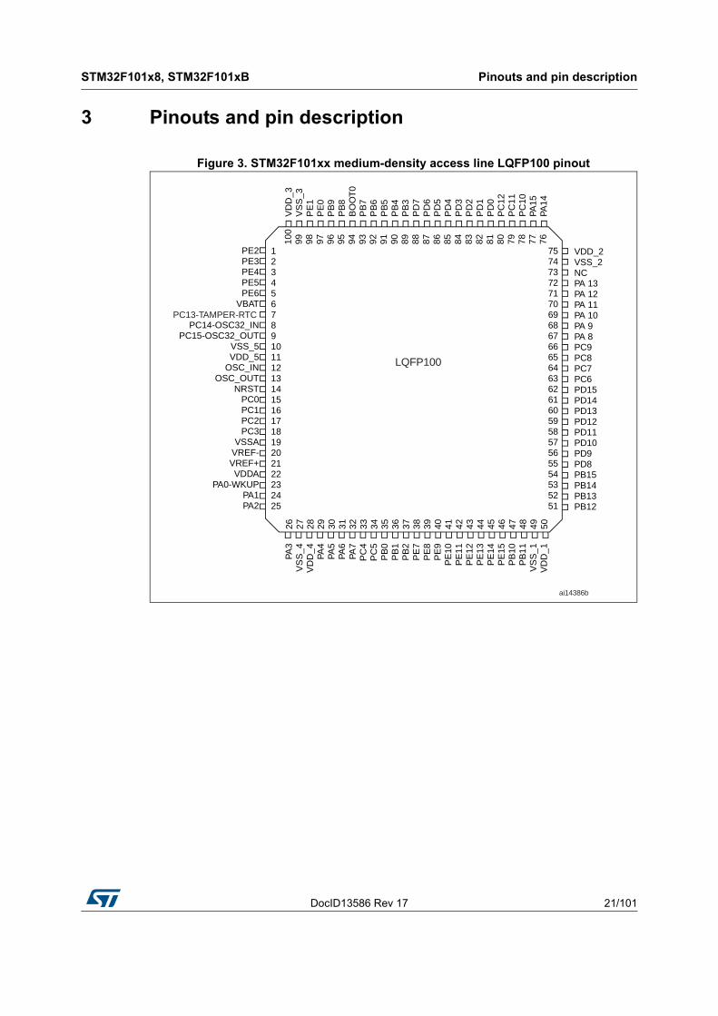
3 Pinouts and pin description
Figure 3. STM32F101xx medium-density access line LQFP100 pinout
100
99 98 97 96 95 94 93 92 91 90 89 88 87 86 85 84 83 82 81 80 79 78 77 76
12345678910111213141516171819202122232425
75747372717069686766656463626160595857565554535251
PE2PE3PE4PE5PE6
VBAT
PC14-OSC32_INPC15-OSC32_OUT
VSS_5VDD_5
OSC_INOSC_OUT
NRSTPC0PC1PC2PC3
VSSAVREF-VREF+VDDA
PA0-WKUPPA1PA2
VDD_2 VSS_2 NC PA 13 PA 12 PA 11 PA 10 PA 9 PA 8 PC9 PC8 PC7 PC6 PD15 PD14 PD13 PD12 PD11 PD10 PD9 PD8 PB15 PB14 PB13 PB12
PA3
VS
S_4
VD
D_4
PA4
PA5
PA6
PA7
PC
4P
C5
PB
0P
B1
PB
2P
E7
PE
8P
E9
PE
10P
E11
PE
12P
E13
PE
14P
E15
PB
10P
B11
VS
S_1
VD
D_1
VD
D_3
V
SS
_3
PE
1
PE
0
PB
9
PB
8
BO
OT
0
PB
7
PB
6
PB
5
PB
4
PB
3
PD
7
PD
6
PD
5
PD
4
PD
3
PD
2
PD
1
PD
0
PC
12
PC
11
PC
10
PA15
PA
14
26 27 28 29 30 31 32 33 34 35 36 37 38 39 40 41 42 43 44 45 46 47 48 49 50
ai14386b
LQFP100
PC13-TAMPER-RTC
Pinouts and pin description STM32F101x8, STM32F101xB
22/101 DocID13586 Rev 17
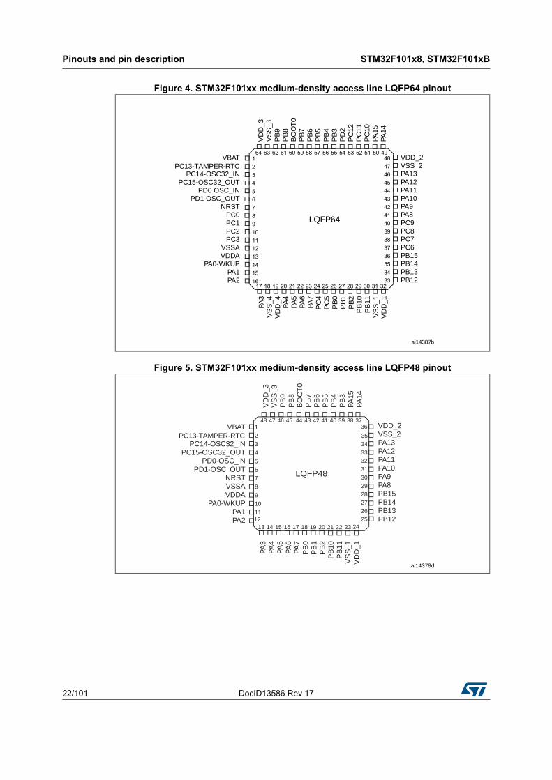
Figure 4. STM32F101xx medium-density access line LQFP64 pinout
Figure 5. STM32F101xx medium-density access line LQFP48 pinout
64 63 62 61 60 59 58 57 56 55 54 53 52 51 50 4948
47
46
45
44
43
42
41
40
39
38
37
36
35
34
3317 18 19 20 21 22 23 24 29 30 31 3225 26 27 28
1
2
3
4
5
6
7
8
9
10
11
12
13
14
15
16
VBAT
PC14-OSC32_INPC15-OSC32_OUT
PD0 OSC_INPD1 OSC_OUT
NRSTPC0PC1PC2PC3
VSSAVDDA
PA0-WKUPPA1PA2
VD
D_3
V
SS
_3
PB
9
PB
8
BO
OT
0
PB
7
PB
6
PB
5
PB
4
PB
3
PD
2
PC
12
PC
11
PC
10
PA15
PA
14
VDD_2 VSS_2 PA13 PA12 PA11 PA10 PA9 PA8 PC9 PC8 PC7 PC6 PB15 PB14 PB13 PB12
PA3
VS
S_4
VD
D_4
PA4
PA5
PA6
PA7
PC
4P
C5
PB
0P
B1
PB
2P
B10
PB
11V
SS
_1V
DD
_1
LQFP64
ai14387b
PC13-TAMPER-RTC
44 43 42 41 40 39 38 3736
35
343332
31
30
2928
27
2625
242312
13 14 15 16 17 18 19 20 21 22
1
2
3
4
5
6
7
8
9
10
11
48 47 46 45
LQFP48
PA3
PA4
PA5
PA6
PA7
PB
0P
B1
PB
2P
B10
PB
11V
SS
_1V
DD
_1
VDD_2 VSS_2 PA13 PA12 PA11 PA10 PA9 PA8 PB15 PB14 PB13 PB12
VBAT
PC14-OSC32_INPC15-OSC32_OUT
PD0-OSC_INPD1-OSC_OUT
NRSTVSSAVDDA
PA0-WKUPPA1PA2
VD
D_3
V
SS
_3
PB
9
PB
8
BO
OT
0
PB
7
PB
6
PB
5
PB
4
PB
3
PA15
PA
14
ai14378d
PC13-TAMPER-RTC
DocID13586 Rev 17 23/101
STM32F101x8, STM32F101xB Pinouts and pin description
100
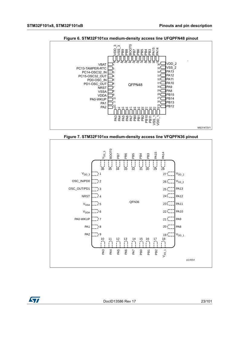
Figure 6. STM32F101xx medium-density access line UFQPFN48 pinout
Figure 7. STM32F101xx medium-density access line VFQPFN36 pinout
VS
S_3
BO
OT
0
PB
7
PB
6
PB
5
PB
4
PB
3
PA15
PA14
36 35 34 33 32 31 30 29 28
VDD_3 1 27 VDD_2
OSC_IN/PD0 2 26 VSS_2
OSC_OUT/PD1 3 25 PA13
NRST 4
QFN36
24 PA12
VSSA 5 23 PA11
VDDA 6 22 PA10
PA0-WKUP 7 21 PA9
PA1 8 20 PA8
PA2 9 19 VDD_1
10 11 12 13 14 15 16 17 18
PA3
PA4
PA5
PA6
PA7
PB
0
PB
1
PB
2
VS
S_1
ai14654
Pinouts and pin description STM32F101x8, STM32F101xB
24/101 DocID13586 Rev 17
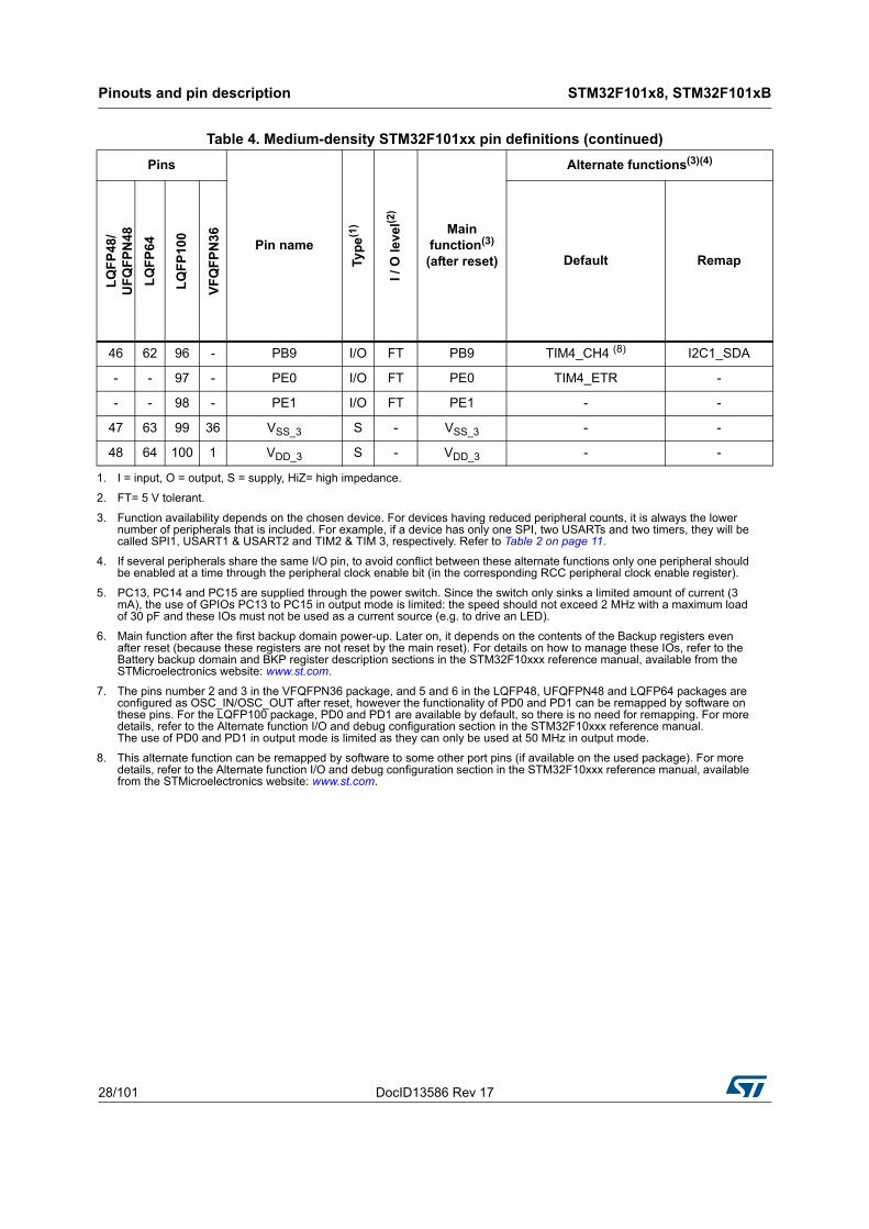
Table 4. Medium-density STM32F101xx pin definitions
Pins
Pin name
Typ
e(1)
I / O
leve
l(2)
Main function(3)
(after reset)
Alternate functions(3)(4)
LQ
FP
48/
UF
QF
PN
48
LQ
FP
64
LQ
FP
100
VF
QF
PN
36
Default Remap
- - 1 - PE2 I/O FT PE2 TRACECLK -
- - 2 - PE3 I/O FT PE3 TRACED0 -
- - 3 - PE4 I/O FT PE4 TRACED1 -
- - 4 - PE5 I/O FT PE5 TRACED2 -
- - 5 - PE6 I/O FT PE6 TRACED3 -
1 1 6 - VBAT S - VBAT - -
2 2 7 -PC13-TAMPER-
RTC(5) I/O - PC13(6) TAMPER-RTC -
3 3 8 -PC14-
OSC32_IN(5) I/O - PC14(6) OSC32_IN -
4 4 9 -PC15-
OSC32_OUT(5) I/O - PC15(6) OSC32_OUT -
- - 10 - VSS_5 S - VSS_5 - -
- - 11 - VDD_5 S - VDD_5 - -
5 5 12 2 OSC_IN I - OSC_IN - PD0(7)
6 6 13 3 OSC_OUT O - OSC_OUT - PD1(7)
7 7 14 4 NRST I/O - NRST - -
- 8 15 - PC0 I/O - PC0 ADC_IN10 -
- 9 16 - PC1 I/O - PC1 ADC_IN11 -
- 10 17 - PC2 I/O - PC2 ADC_IN12 -
- 11 18 - PC3 I/O - PC3 ADC_IN13 -
8 12 19 5 VSSA S - VSSA - -
- - 20 - VREF- S - VREF- - -
- - 21 - VREF+ S - VREF+ - -
9 13 22 6 VDDA S - VDDA - -
10 14 23 7 PA0-WKUP I/O - PA0WKUP/USART2_CTS(8)/
ADC_IN0/TIM2_CH1_ETR(8)
-
11 15 24 8 PA1 I/O - PA1USART2_RTS(8)/
ADC_IN1/TIM2_CH2(8) -
DocID13586 Rev 17 25/101
STM32F101x8, STM32F101xB Pinouts and pin description
100
12 16 25 9 PA2 I/O - PA2USART2_TX(8)/
ADC_IN2/TIM2_CH3(8) -
13 17 26 10 PA3 I/O - PA3USART2_RX(8)/
ADC_IN3/TIM2_CH4(8) -
- 18 27 - VSS_4 S - VSS_4 - -
- 19 28 - VDD_4 S - VDD_4 - -
14 20 29 11 PA4 I/O - PA4SPI1_NSS(8)/ADC_IN4
USART2_CK(8)/ -
15 21 30 12 PA5 I/O - PA5 SPI1_SCK(8)/ADC_IN5 -
16 22 31 13 PA6 I/O - PA6SPI1_MISO(8)/ADC_IN6
TIM3_CH1(8) -
17 23 32 14 PA7 I/O - PA7SPI1_MOSI(8)/ADC_IN7
TIM3_CH2(8) -
- 24 33 - PC4 I/O - PC4 ADC_IN14 -
- 25 34 - PC5 I/O - PC5 ADC_IN15 -
18 26 35 15 PB0 I/O - PB0 ADC_IN8/TIM3_CH3(8) -
19 27 36 16 PB1 I/O - PB1 ADC_IN9/TIM3_CH4(8) -
20 28 37 17 PB2 I/O FT PB2/BOOT1 - -
- - 38 - PE7 I/O FT PE7 - -
- - 39 - PE8 I/O FT PE8 - -
- - 40 - PE9 I/O FT PE9 - -
- - 41 - PE10 I/O FT PE10 - -
- - 42 - PE11 I/O FT PE11 - -
- - 43 - PE12 I/O FT PE12 - -
- - 44 - PE13 I/O FT PE13 - -
- - 45 - PE14 I/O FT PE14 - -
- - 46 - PE15 I/O FT PE15 - -
21 29 47 - PB10 I/O FT PB10I2C2_SCL/
USART3_TX (8) TIM2_CH3
22 30 48 - PB11 I/O FT PB11I2C2_SDA/
USART3_RX (8) TIM2_CH4
Table 4. Medium-density STM32F101xx pin definitions (continued)
Pins
Pin name
Typ
e(1)
I / O
leve
l(2)
Main function(3)
(after reset)
Alternate functions(3)(4)
LQ
FP
48/
UF
QF
PN
48
LQ
FP
64
LQ
FP
100
VF
QF
PN
36
Default Remap
Pinouts and pin description STM32F101x8, STM32F101xB
26/101 DocID13586 Rev 17
23 31 49 18 VSS_1 S - VSS_1 - -
24 32 50 19 VDD_1 S - VDD_1 - -
25 33 51 - PB12 I/O FT PB12SPI2_NSS / I2C2_SMBA
/ USART3_CK (8) -
26 34 52 - PB13 I/O FT PB13SPI2_SCK/
USART3_CTS(8) -
27 35 53 - PB14 I/O FT PB14SPI2_MISO/
USART3_RTS(8) -
28 36 54 - PB15 I/O FT PB15 SPI2_MOSI -
- - 55 - PD8 I/O FT PD8 - USART3_TX
- - 56 - PD9 I/O FT PD9 - USART3_RX
- - 57 - PD10 I/O FT PD10 - USART3_CK
- - 58 - PD11 I/O FT PD11 - USART3_CTS
- - 59 - PD12 I/O FT PD12 -TIM4_CH1 /
USART3_RTS
- - 60 - PD13 I/O FT PD13 - TIM4_CH2
- - 61 - PD14 I/O FT PD14 - TIM4_CH3
- - 62 - PD15 I/O FT PD15 - TIM4_CH4
- 37 63 - PC6 I/O FT PC6 - TIM3_CH1
- 38 64 - PC7 I/O FT PC7 - TIM3_CH2
- 39 65 - PC8 I/O FT PC8 - TIM3_CH3
- 40 66 - PC9 I/O FT PC9 - TIM3_CH4
29 41 67 20 PA8 I/O FT PA8 USART1_CK/MCO -
30 42 68 21 PA9 I/O FT PA9 USART1_TX(8) -
31 43 69 22 PA10 I/O FT PA10 USART1_RX(8) -
32 44 70 23 PA11 I/O FT PA11 USART1_CTS -
33 45 71 24 PA12 I/O FT PA12 USART1_RTS -
34 46 72 25 PA13 I/O FTJTMS-SWDIO
- PA13
- - 73 - Not connected -
Table 4. Medium-density STM32F101xx pin definitions (continued)
Pins
Pin name
Typ
e(1)
I / O
leve
l(2)
Main function(3)
(after reset)
Alternate functions(3)(4)
LQ
FP
48/
UF
QF
PN
48
LQ
FP
64
LQ
FP
100
VF
QF
PN
36
Default Remap
DocID13586 Rev 17 27/101
STM32F101x8, STM32F101xB Pinouts and pin description
100
35 47 74 26 VSS_2 S - VSS_2 - -
36 48 75 27 VDD_2 S - VDD_2 - -
37 49 76 28 PA14 I/O FTJTCK/SWCL
K- PA14
38 50 77 29 PA15 I/O FT JTDI -TIM2_CH1_ETR
/ PA15/ SPI1_NSS
- 51 78 - PC10 I/O FT PC10 - USART3_TX
- 52 79 - PC11 I/O FT PC11 - USART3_RX
- 53 80 - PC12 I/O FT PC12 - USART3_CK
- - 81 2 PD0 I/O FT PD0 - -
- - 82 3 PD1 I/O FT PD1 - -
- 54 83 - PD2 I/O FT PD2 TIM3_ETR -
- - 84 - PD3 I/O FT PD3 - USART2_CTS
- - 85 - PD4 I/O FT PD4 - USART2_RTS
- - 86 - PD5 I/O FT PD5 - USART2_TX
- - 87 - PD6 I/O FT PD6 - USART2_RX
- - 88 - PD7 I/O FT PD7 - USART2_CK
39 55 89 30 PB3 I/O FT JTDO TIM2_CH2 / PB3
TRACESWOSPI1_SCK
40 56 90 31 PB4 I/O FT JNTRST -PB4 / TIM3_CH1
SPI1_MISO
41 57 91 32 PB5 I/O - PB5 I2C1_SMBAl TIM3_CH2 / SPI1_MOSI
42 58 92 33 PB6 I/O FT PB6I2C1_SCL(8)/TIM4_CH1 (8) USART1_TX
43 59 93 34 PB7 I/O FT PB7I2C1_SDA(8)/TIM4_CH2 (8) USART1_RX
44 60 94 35 BOOT0 I - BOOT0 - -
45 61 95 - PB8 I/O FT PB8 TIM4_CH3 (8) I2C1_SCL
Table 4. Medium-density STM32F101xx pin definitions (continued)
Pins
Pin name
Typ
e(1)
I / O
leve
l(2)
Main function(3)
(after reset)
Alternate functions(3)(4)
LQ
FP
48/
UF
QF
PN
48
LQ
FP
64
LQ
FP
100
VF
QF
PN
36
Default Remap
Pinouts and pin description STM32F101x8, STM32F101xB
28/101 DocID13586 Rev 17
46 62 96 - PB9 I/O FT PB9 TIM4_CH4 (8) I2C1_SDA
- - 97 - PE0 I/O FT PE0 TIM4_ETR -
- - 98 - PE1 I/O FT PE1 - -
47 63 99 36 VSS_3 S - VSS_3 - -
48 64 100 1 VDD_3 S - VDD_3 - -
1. I = input, O = output, S = supply, HiZ= high impedance.
2. FT= 5 V tolerant.
3. Function availability depends on the chosen device. For devices having reduced peripheral counts, it is always the lower number of peripherals that is included. For example, if a device has only one SPI, two USARTs and two timers, they will be called SPI1, USART1 & USART2 and TIM2 & TIM 3, respectively. Refer to Table 2 on page 11.
4. If several peripherals share the same I/O pin, to avoid conflict between these alternate functions only one peripheral should be enabled at a time through the peripheral clock enable bit (in the corresponding RCC peripheral clock enable register).
5. PC13, PC14 and PC15 are supplied through the power switch. Since the switch only sinks a limited amount of current (3 mA), the use of GPIOs PC13 to PC15 in output mode is limited: the speed should not exceed 2 MHz with a maximum load of 30 pF and these IOs must not be used as a current source (e.g. to drive an LED).
6. Main function after the first backup domain power-up. Later on, it depends on the contents of the Backup registers even after reset (because these registers are not reset by the main reset). For details on how to manage these IOs, refer to the Battery backup domain and BKP register description sections in the STM32F10xxx reference manual, available from the STMicroelectronics website: www.st.com.
7. The pins number 2 and 3 in the VFQFPN36 package, and 5 and 6 in the LQFP48, UFQFPN48 and LQFP64 packages are configured as OSC_IN/OSC_OUT after reset, however the functionality of PD0 and PD1 can be remapped by software on these pins. For the LQFP100 package, PD0 and PD1 are available by default, so there is no need for remapping. For more details, refer to the Alternate function I/O and debug configuration section in the STM32F10xxx reference manual.The use of PD0 and PD1 in output mode is limited as they can only be used at 50 MHz in output mode.
8. This alternate function can be remapped by software to some other port pins (if available on the used package). For more details, refer to the Alternate function I/O and debug configuration section in the STM32F10xxx reference manual, available from the STMicroelectronics website: www.st.com.
Table 4. Medium-density STM32F101xx pin definitions (continued)
Pins
Pin name
Typ
e(1)
I / O
leve
l(2)
Main function(3)
(after reset)
Alternate functions(3)(4)
LQ
FP
48/
UF
QF
PN
48
LQ
FP
64
LQ
FP
100
VF
QF
PN
36
Default Remap
DocID13586 Rev 17 29/101
STM32F101x8, STM32F101xB Memory mapping
100
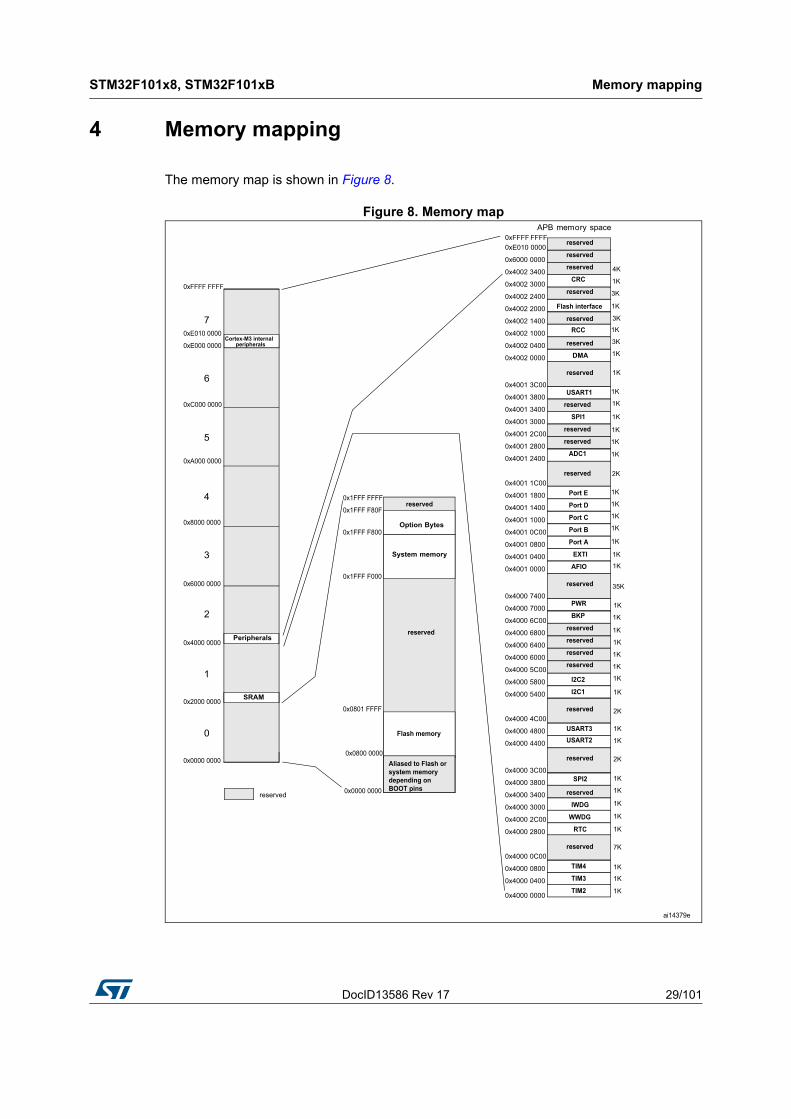
4 Memory mapping
The memory map is shown in Figure 8.
Figure 8. Memory map
Electrical characteristics STM32F101x8, STM32F101xB
30/101 DocID13586 Rev 17
5 Electrical characteristics
5.1 Parameter conditions
Unless otherwise specified, all voltages are referenced to VSS.
5.1.1 Minimum and maximum values
Unless otherwise specified the minimum and maximum values are guaranteed in the worst conditions of ambient temperature, supply voltage and frequencies by tests in production on 100% of the devices with an ambient temperature at TA = 25 °C and TA = TAmax (given by the selected temperature range).
Data based on characterization results, design simulation and/or technology characteristics are indicated in the table footnotes and are not tested in production. Based on characterization, the minimum and maximum values refer to sample tests and represent the mean value plus or minus three times the standard deviation (mean±3).
5.1.2 Typical values
Unless otherwise specified, typical data are based on TA = 25 °C, VDD = 3.3 V (for the 2 V VDD 3.6 V voltage range). They are given only as design guidelines and are not tested.
Typical ADC accuracy values are determined by characterization of a batch of samples from a standard diffusion lot over the full temperature range, where 95% of the devices have an error less than or equal to the value indicated (mean±2).
5.1.3 Typical curves
Unless otherwise specified, all typical curves are given only as design guidelines and are not tested.
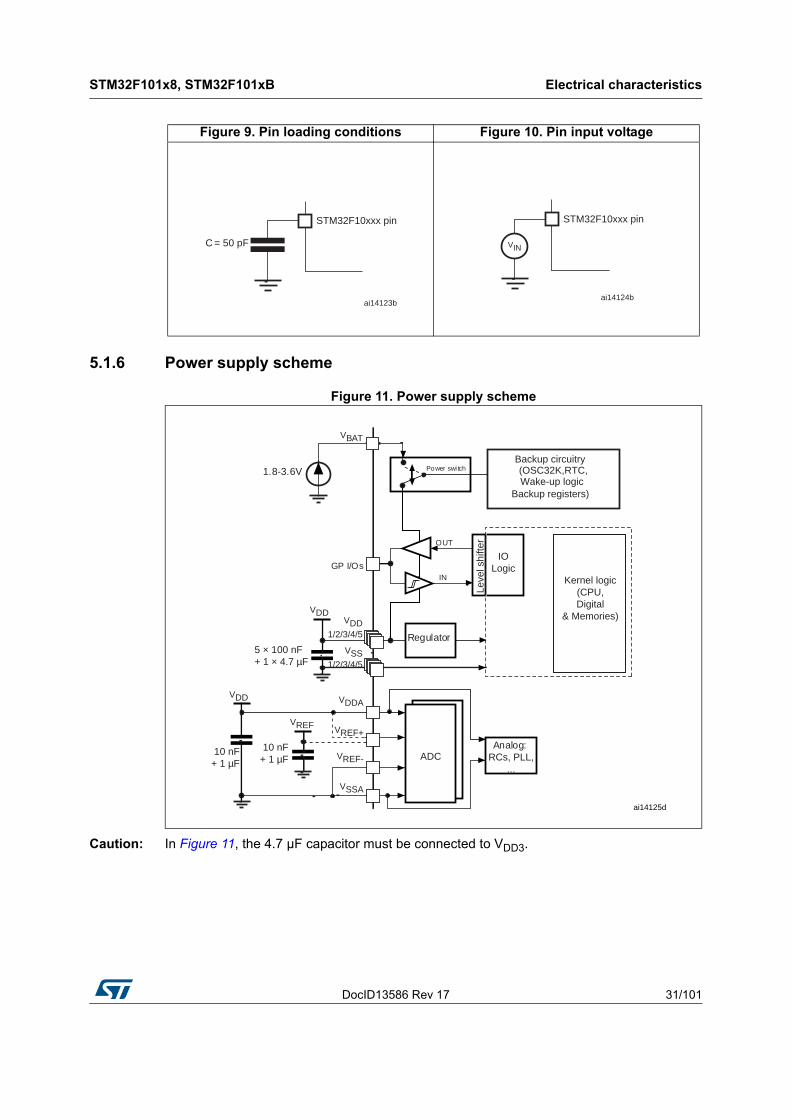
5.1.4 Loading capacitor
The loading conditions used for pin parameter measurement are shown in Figure 9.
5.1.5 Pin input voltage
The input voltage measurement on a pin of the device is described in Figure 10.
DocID13586 Rev 17 31/101
STM32F101x8, STM32F101xB Electrical characteristics
100
5.1.6 Power supply scheme
Figure 11. Power supply scheme
Caution: In Figure 11, the 4.7 µF capacitor must be connected to VDD3.
Figure 9. Pin loading conditions Figure 10. Pin input voltage
ai14123b
C = 50 pF
STM32F10xxx pin
ai14124b
STM32F10xxx pin
VIN
ai14125d
VDD1/2/3/4/5
Analog: RCs, PLL,
...
Power swi tch
VBAT
GP I/Os
OUT
IN Kernel logic (CPU, Digital
& Memories)
Backup circuitry(OSC32K,RTC,
Backup registers)Wake-up logic
5 × 100 nF+ 1 × 4.7 µF
1.8-3.6V
RegulatorVSS
1/2/3/4/5
VDDA
VREF+
VREF-
VSSA
ADC
Leve
l shi
fter
IOLogic
VDD
10 nF+ 1 µF
VREF
10 nF+ 1 µF
VDD
Electrical characteristics STM32F101x8, STM32F101xB
32/101 DocID13586 Rev 17
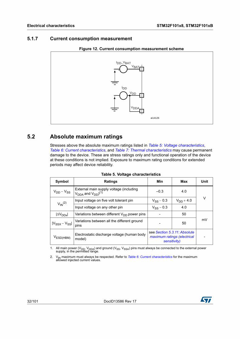
5.1.7 Current consumption measurement
Figure 12. Current consumption measurement scheme
5.2 Absolute maximum ratings
Stresses above the absolute maximum ratings listed in Table 5: Voltage characteristics, Table 6: Current characteristics, and Table 7: Thermal characteristics may cause permanent damage to the device. These are stress ratings only and functional operation of the device at these conditions is not implied. Exposure to maximum rating conditions for extended periods may affect device reliability.
ai14126
VBAT
VDD
VDDA
IDD_VBAT
IDD
Table 5. Voltage characteristics
Symbol Ratings Min Max Unit
VDD VSSExternal main supply voltage (including VDDA and VDD)(1)
1. All main power (VDD, VDDA) and ground (VSS, VSSA) pins must always be connected to the external power supply, in the permitted range.
–0.3 4.0
V
VIN(2)
2. VIN maximum must always be respected. Refer to Table 6: Current characteristics for the maximum allowed injected current values.
Input voltage on five volt tolerant pin VSS 0.3 VDD 4.0
Input voltage on any other pin VSS 0.3 4.0
|VDDx| Variations between different VDD power pins - 50
mV|VSSX VSS|
Variations between all the different ground pins
- 50
VESD(HBM)Electrostatic discharge voltage (human body model)
see Section 5.3.11: Absolute maximum ratings (electrical
sensitivity)-
DocID13586 Rev 17 33/101
STM32F101x8, STM32F101xB Electrical characteristics
100
5.3 Operating conditions
5.3.1 General operating conditions
Table 6. Current characteristics
Symbol Ratings Max. Unit
IVDD Total current into VDD/VDDA power lines (source)(1)
1. All main power (VDD, VDDA) and ground (VSS, VSSA) pins must always be connected to the external power supply, in the permitted range.
150
mA
IVSS Total current out of VSS ground lines (sink)(1) 150
IIOOutput current sunk by any I/O and control pin 25
Output current source by any I/Os and control pin 25
IINJ(PIN)(2)
2. Negative injection disturbs the analog performance of the device. See note in Section 5.3.17: 12-bit ADC characteristics.
Injected current on five volt tolerant pins(3)
3. Positive injection is not possible on these I/Os. A negative injection is induced by VIN<VSS. IINJ(PIN) must never be exceeded. Refer to Table 5: Voltage characteristics for the maximum allowed input voltage values.
-5/+0
Injected current on any other pin(4)
4. A positive injection is induced by VIN>VDD while a negative injection is induced by VIN<VSS. IINJ(PIN) must never be exceeded. Refer to Table 5: Voltage characteristics for the maximum allowed input voltage values.
± 5
IINJ(PIN) Total injected current (sum of all I/O and control pins)(5)
5. When several inputs are submitted to a current injection, the maximum IINJ(PIN) is the absolute sum of the positive and negative injected currents (instantaneous values).
± 25
Table 7. Thermal characteristics
Symbol Ratings Value Unit
TSTG Storage temperature range –65 to +150 °C
TJ Maximum junction temperature 150 °C
Table 8. General operating conditions
Symbol Parameter Conditions Min Max Unit
fHCLK Internal AHB clock frequency - 0 36
MHzfPCLK1 Internal APB1 clock frequency - 0 36
fPCLK2 Internal APB2 clock frequency - 0 36
VDD Standard operating voltage - 2 3.6
VVDDA(1)
Analog operating voltage(ADC not used) Must be the same potential
as VDD(2)
2 3.6
Analog operating voltage(ADC used)
2.4 3.6
VBAT Backup operating voltage - 1.8 3.6
Electrical characteristics STM32F101x8, STM32F101xB
34/101 DocID13586 Rev 17
5.3.2 Operating conditions at power-up / power-down
Subject to general operating conditions for TA.
5.3.3 Embedded reset and power control block characteristics
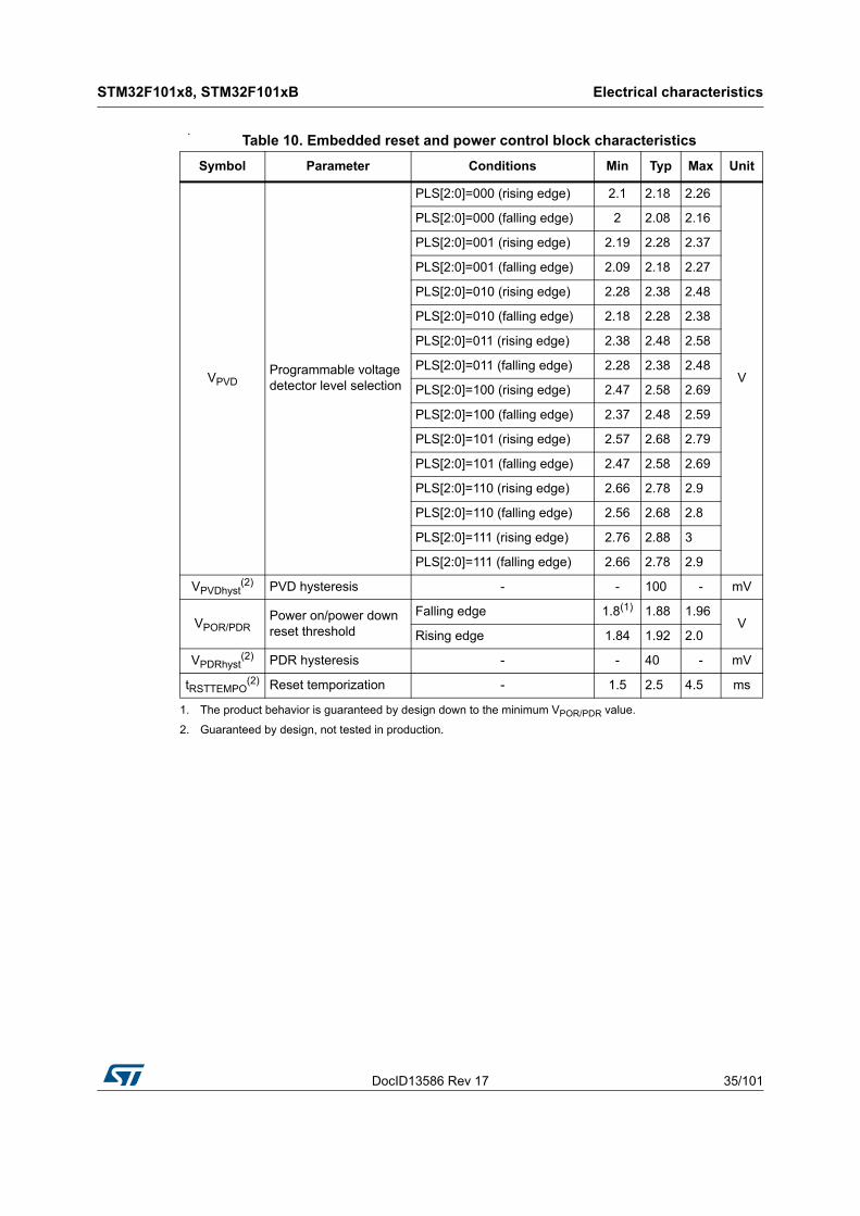
The parameters given in Table 10 are derived from tests performed under the ambient temperature and VDD supply voltage conditions summarized in Table 8.
VIN I/O input voltage
Standard IO –0.3 VDD + 0.3
VFT IO(3)2 V < VDD 3.6 V –0.3 5.5
VDD = 2 V –0.3 5.2
BOOT0 0 5.5
PDPower dissipation at TA = 85 °C (4)
LQFP100 - 434
mW
LQFP64 - 444
LQFP48 - 363
UFQFPN48 - 624
VFQFPN36 - 1000
TA Ambient temperatureMaximum power dissipation –40 85
°C Low power dissipation(5) –40 105
TJ Junction temperature range - –40 105
1. When the ADC is used, refer to Table 41: ADC characteristics.
2. It is recommended to power VDD and VDDA from the same source. A maximum difference of 300 mV between VDD and VDDA can be tolerated during power-up and operation.
3. To sustain a voltage higher than VDD+0.3 V, the internal pull-up/pull-down resistors must be disabled.
4. If TA is lower, higher PD values are allowed as long as TJ does not exceed TJmax (see Table 6.7: Thermal characteristics on page 90).
5. In low power dissipation state, TA can be extended to this range as long as TJ does not exceed TJmax (see Table 6.7: Thermal characteristics on page 90).
Table 8. General operating conditions (continued)
Symbol Parameter Conditions Min Max Unit
Table 9. Operating conditions at power-up / power-down
Symbol Parameter Conditions Min Max Unit
tVDD
VDD rise time rate
-
0 ∞
µs/VVDD fall time
rate20 ∞
DocID13586 Rev 17 35/101
STM32F101x8, STM32F101xB Electrical characteristics
100
.
Table 10. Embedded reset and power control block characteristics
Symbol Parameter Conditions Min Typ Max Unit
VPVDProgrammable voltage detector level selection
PLS[2:0]=000 (rising edge) 2.1 2.18 2.26
V
PLS[2:0]=000 (falling edge) 2 2.08 2.16
PLS[2:0]=001 (rising edge) 2.19 2.28 2.37
PLS[2:0]=001 (falling edge) 2.09 2.18 2.27
PLS[2:0]=010 (rising edge) 2.28 2.38 2.48
PLS[2:0]=010 (falling edge) 2.18 2.28 2.38
PLS[2:0]=011 (rising edge) 2.38 2.48 2.58
PLS[2:0]=011 (falling edge) 2.28 2.38 2.48
PLS[2:0]=100 (rising edge) 2.47 2.58 2.69
PLS[2:0]=100 (falling edge) 2.37 2.48 2.59
PLS[2:0]=101 (rising edge) 2.57 2.68 2.79
PLS[2:0]=101 (falling edge) 2.47 2.58 2.69
PLS[2:0]=110 (rising edge) 2.66 2.78 2.9
PLS[2:0]=110 (falling edge) 2.56 2.68 2.8
PLS[2:0]=111 (rising edge) 2.76 2.88 3
PLS[2:0]=111 (falling edge) 2.66 2.78 2.9
VPVDhyst(2) PVD hysteresis - - 100 - mV
VPOR/PDRPower on/power down reset threshold
Falling edge 1.8(1)
1. The product behavior is guaranteed by design down to the minimum VPOR/PDR value.
1.88 1.96V
Rising edge 1.84 1.92 2.0
VPDRhyst(2) PDR hysteresis - - 40 - mV
tRSTTEMPO(2)
2. Guaranteed by design, not tested in production.
Reset temporization - 1.5 2.5 4.5 ms
Electrical characteristics STM32F101x8, STM32F101xB
36/101 DocID13586 Rev 17
5.3.4 Embedded reference voltage
The parameters given in Table 11 are derived from tests performed under the ambient temperature and VDD supply voltage conditions summarized in Table 8.
5.3.5 Supply current characteristics
The current consumption is a function of several parameters and factors such as the operating voltage, ambient temperature, I/O pin loading, device software configuration, operating frequencies, I/O pin switching rate, program location in memory and executed binary code.The current consumption is measured as described in Figure 12: Current consumption measurement scheme.All Run-mode current consumption measurements given in this section are performed with a reduced code that gives a consumption equivalent to Dhrystone 2.1 code.
Maximum current consumption
The MCU is placed under the following conditions:
All I/O pins are in input mode with a static value at VDD or VSS (no load)
All peripherals are disabled except if it is explicitly mentioned
The Flash access time is adjusted to fHCLK frequency (0 wait state from 0 to 24 MHz, 1 wait state from 24 to 36 MHz)
Prefetch in on (reminder: this bit must be set before clock setting and bus prescaling)
When the peripherals are enabled fPCLK1 = fHCLK/2, fPCLK2 = fHCLK
The parameters given in Table 12 are derived from tests performed under the ambient temperature and VDD supply voltage conditions summarized in Table 8.
Table 11. Embedded internal reference voltage
Symbol Parameter Conditions Min Typ Max Unit
VREFINT Internal reference voltage –40 °C < TA < +85 °C 1.16 1.20 1.24 V
TS_vrefint(1)
1. Shortest sampling time can be determined in the application by multiple iterations.
ADC sampling time when reading the internal reference voltage
- - 5.1 17.1(2)
2. Guaranteed by design, not tested in production.
µs
VRERINT(2) Internal reference voltage spread
over the temperature rangeVDD = 3 V ±10 mV - - 10 mV
TCoeff(2) Temperature coefficient - - - 100
ppm/°C
DocID13586 Rev 17 37/101
STM32F101x8, STM32F101xB Electrical characteristics
100
Table 12. Maximum current consumption in Run mode, code with data processingrunning from Flash
Symbol Parameter Conditions fHCLK
Max(1)
1. Based on characterization, not tested in production.
UnitTA = 85 °C
IDDSupply current in Run mode
External clock (2), all peripherals enabled
2. External clock is 8 MHz and PLL is on when fHCLK > 8 MHz.
36 MHz 28.6
mA
24 MHz 19.9
16 MHz 14.7
8 MHz 8.6
External clock (2), all peripherals Disabled
36 MHz 19.8
24 MHz 13.9
16 MHz 10.7
8 MHz 6.8
Table 13. Maximum current consumption in Run mode, code with data processingrunning from RAM
Symbol Parameter Conditions fHCLK
Max(1)
1. Based on characterization, tested in production at VDD max, fHCLK max.
UnitTA = 85 °C
IDDSupply current in Run mode
External clock (2), all peripherals enabled
2. External clock is 8 MHz and PLL is on when fHCLK > 8 MHz.
36 MHz 24
mA
24 MHz 17.5
16 MHz 12.5
8 MHz 7.5
External clock(2) all peripherals disabled
36 MHz 16
24 MHz 11.5
16 MHz 8.5
8 MHz 5.5
Electrical characteristics STM32F101x8, STM32F101xB
38/101 DocID13586 Rev 17
Figure 13. Typical current consumption in Run mode versus frequency (at 3.6 V) -code with data processing running from RAM, peripherals enabled
Figure 14. Typical current consumption in Run mode versus frequency (at 3.6 V) -code with data processing running from RAM, peripherals disabled
DocID13586 Rev 17 39/101
STM32F101x8, STM32F101xB Electrical characteristics
100
Table 14. Maximum current consumption in Sleep mode, code running from Flashor RAM
Symbol Parameter Conditions fHCLK
Max(1)
1. Based on characterization, tested in production at VDD max and fHCLK max with peripherals enabled.
UnitTA = 85 °C
IDDSupply current in Sleep mode
External clock(2) all peripherals enabled
2. External clock is 8 MHz and PLL is on when fHCLK > 8 MHz.
36 MHz 15.5
mA
24 MHz 11.5
16 MHz 8.5
8 MHz 5.5
External clock(2), all peripherals disabled
36 MHz 5
24 MHz 4.5
16 MHz 4
8 MHz 3
Table 15. Typical and maximum current consumptions in Stop and Standby modes
Symbol Parameter Conditions
Typ(1) Max
UnitVDD/VB
AT= 2.0 V
VDD/ VBAT = 2.4 V
VDD/VB
AT= 3.3 V
TA = 85 °C(2)
IDD
Supply current in Stop mode
Regulator in Run mode, Low-speed and high-speed internal RC oscillators and high-speed oscillator OFF (no independent watchdog)
- 23.5 24 200
µA
Regulator in Low-Power mode, Low-speed and high-speed internal RC oscillators and high-speed oscillator OFF (no independent watchdog)
- 13.5 14 180
Supply current in Standby mode
Low-speed internal RC oscillator and independent watchdog ON
- 2.6 3.4 -
Low-speed internal RC oscillator ON, independent watchdog OFF
- 2.4 3.2 -
Low-speed internal RC oscillator and independent watchdog OFF, low-speed oscillator and RTC OFF
- 1.7 2 4
IDD_VBA
T
Backup domain supply current
Low-speed oscillator and RTC ON 0.9 1.1 1.4 1.9
1. Typical values are measured at TA = 25 °C.
2. Based on characterization, not rested in production.
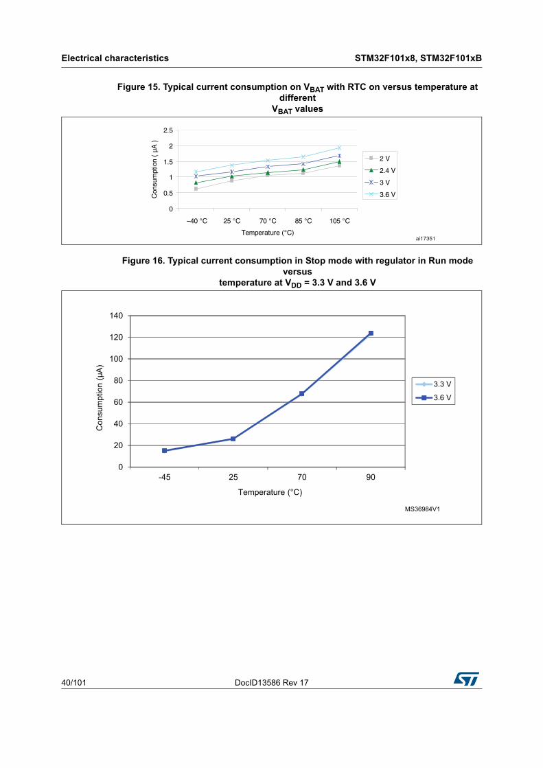
Electrical characteristics STM32F101x8, STM32F101xB
40/101 DocID13586 Rev 17
Figure 15. Typical current consumption on VBAT with RTC on versus temperature at different
VBAT values
Figure 16. Typical current consumption in Stop mode with regulator in Run mode versus
temperature at VDD = 3.3 V and 3.6 V
0
0.5
1
1.5
2
2.5
–40 °C 25 °C 70 °C 85 °C 105 °C
Temperature (°C)
Con
sum
ptio
n (
µA )
2 V
2.4 V
3 V
3.6 V
ai17351
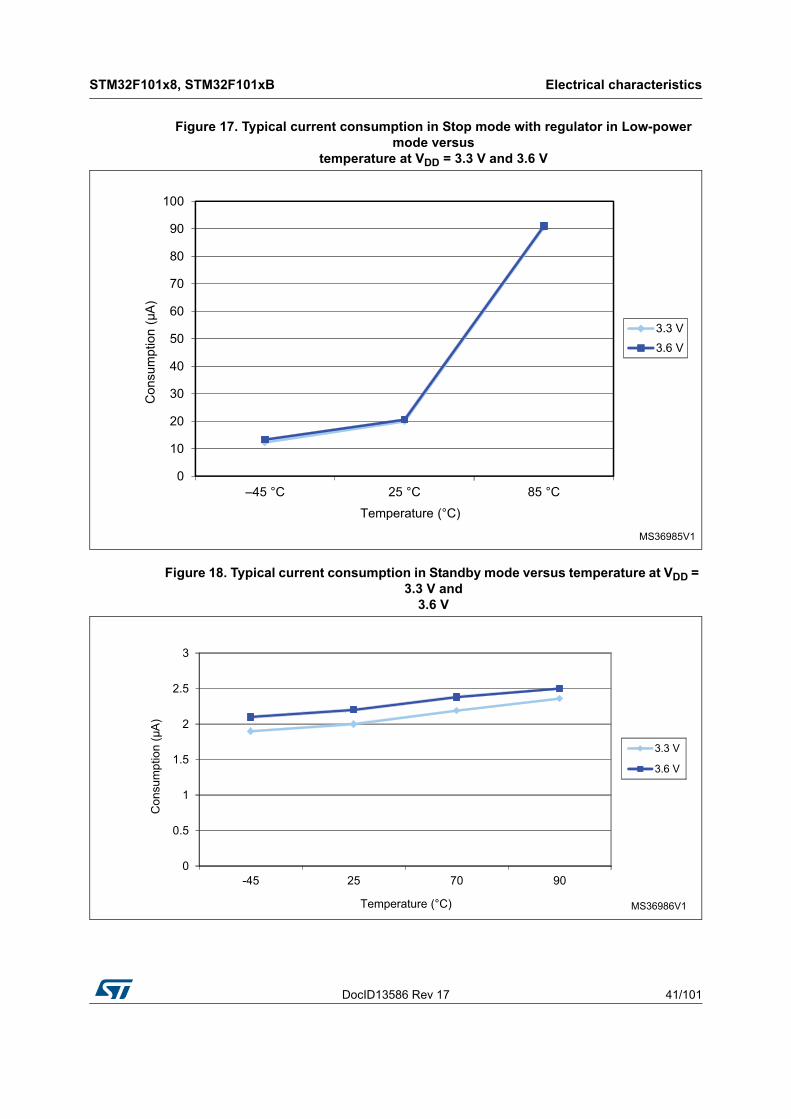
DocID13586 Rev 17 41/101
STM32F101x8, STM32F101xB Electrical characteristics
100
Figure 17. Typical current consumption in Stop mode with regulator in Low-power mode versus
temperature at VDD = 3.3 V and 3.6 V
Figure 18. Typical current consumption in Standby mode versus temperature at VDD = 3.3 V and
3.6 V
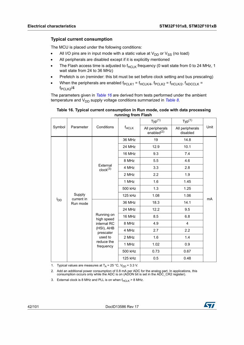
Electrical characteristics STM32F101x8, STM32F101xB
42/101 DocID13586 Rev 17
Typical current consumption
The MCU is placed under the following conditions:
All I/O pins are in input mode with a static value at VDD or VSS (no load)
All peripherals are disabled except if it is explicitly mentioned
The Flash access time is adjusted to fHCLK frequency (0 wait state from 0 to 24 MHz, 1 wait state from 24 to 36 MHz)
Prefetch is on (reminder: this bit must be set before clock setting and bus prescaling)
When the peripherals are enabled fPCLK1 = fHCLK/4, fPCLK2 = fHCLK/2, fADCCLK = fPCLK2/4
The parameters given in Table 16 are derived from tests performed under the ambient temperature and VDD supply voltage conditions summarized in Table 8.
Table 16. Typical current consumption in Run mode, code with data processingrunning from Flash
Symbol Parameter Conditions fHCLK
Typ(1)
1. Typical values are measures at TA = 25 °C, VDD = 3.3 V.
Typ(1)
UnitAll peripherals enabled(2)
2. Add an additional power consumption of 0.8 mA per ADC for the analog part. In applications, this consumption occurs only while the ADC is on (ADON bit is set in the ADC_CR2 register).
All peripherals disabled
IDD
Supply current in Run mode
External clock(3)
3. External clock is 8 MHz and PLL is on when fHCLK > 8 MHz.
36 MHz 19 14.8
mA
24 MHz 12.9 10.1
16 MHz 9.3 7.4
8 MHz 5.5 4.6
4 MHz 3.3 2.8
2 MHz 2.2 1.9
1 MHz 1.6 1.45
500 kHz 1.3 1.25
125 kHz 1.08 1.06
Running on high speed internal RC (HSI), AHB prescaler used to
reduce the frequency
36 MHz 18.3 14.1
24 MHz 12.2 9.5
16 MHz 8.5 6.8
8 MHz 4.9 4
4 MHz 2.7 2.2
2 MHz 1.6 1.4
1 MHz 1.02 0.9
500 kHz 0.73 0.67
125 kHz 0.5 0.48
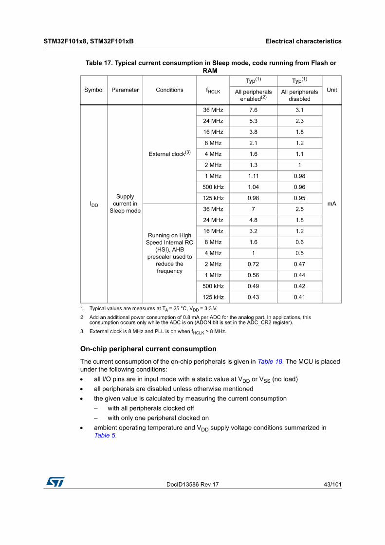
DocID13586 Rev 17 43/101
STM32F101x8, STM32F101xB Electrical characteristics
100
On-chip peripheral current consumption
The current consumption of the on-chip peripherals is given in Table 18. The MCU is placed under the following conditions:
all I/O pins are in input mode with a static value at VDD or VSS (no load)
all peripherals are disabled unless otherwise mentioned
the given value is calculated by measuring the current consumption
– with all peripherals clocked off
– with only one peripheral clocked on
ambient operating temperature and VDD supply voltage conditions summarized in Table 5.
Table 17. Typical current consumption in Sleep mode, code running from Flash or RAM
Symbol Parameter Conditions fHCLK
Typ(1)
1. Typical values are measures at TA = 25 °C, VDD = 3.3 V.
Typ(1)
UnitAll peripherals enabled(2)
2. Add an additional power consumption of 0.8 mA per ADC for the analog part. In applications, this consumption occurs only while the ADC is on (ADON bit is set in the ADC_CR2 register).
All peripherals disabled
IDD
Supply current in
Sleep mode
External clock(3)
3. External clock is 8 MHz and PLL is on when fHCLK > 8 MHz.
36 MHz 7.6 3.1
mA
24 MHz 5.3 2.3
16 MHz 3.8 1.8
8 MHz 2.1 1.2
4 MHz 1.6 1.1
2 MHz 1.3 1
1 MHz 1.11 0.98
500 kHz 1.04 0.96
125 kHz 0.98 0.95
Running on High Speed Internal RC
(HSI), AHB prescaler used to
reduce the frequency
36 MHz 7 2.5
24 MHz 4.8 1.8
16 MHz 3.2 1.2
8 MHz 1.6 0.6
4 MHz 1 0.5
2 MHz 0.72 0.47
1 MHz 0.56 0.44
500 kHz 0.49 0.42
125 kHz 0.43 0.41
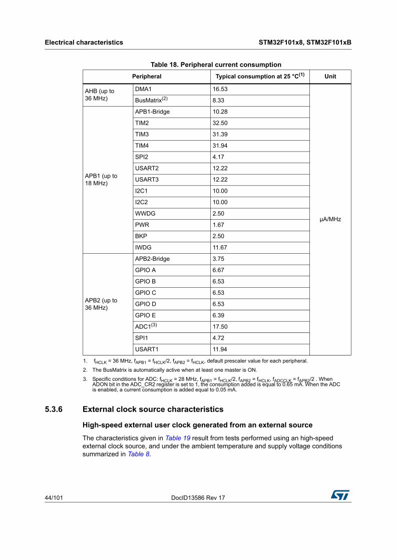
Electrical characteristics STM32F101x8, STM32F101xB
44/101 DocID13586 Rev 17
5.3.6 External clock source characteristics
High-speed external user clock generated from an external source
The characteristics given in Table 19 result from tests performed using an high-speed external clock source, and under the ambient temperature and supply voltage conditions summarized in Table 8.
Table 18. Peripheral current consumption
Peripheral Typical consumption at 25 °C(1)
1. fHCLK = 36 MHz, fAPB1 = fHCLK/2, fAPB2 = fHCLK, default prescaler value for each peripheral.
Unit
AHB (up to 36 MHz)
DMA1 16.53
μA/MHz
BusMatrix(2)
2. The BusMatrix is automatically active when at least one master is ON.
8.33
APB1 (up to 18 MHz)
APB1-Bridge 10.28
TIM2 32.50
TIM3 31.39
TIM4 31.94
SPI2 4.17
USART2 12.22
USART3 12.22
I2C1 10.00
I2C2 10.00
WWDG 2.50
PWR 1.67
BKP 2.50
IWDG 11.67
APB2 (up to 36 MHz)
APB2-Bridge 3.75
GPIO A 6.67
GPIO B 6.53
GPIO C 6.53
GPIO D 6.53
GPIO E 6.39
ADC1(3)
3. Specific conditions for ADC: fHCLK = 28 MHz, fAPB1 = fHCLK/2, fAPB2 = fHCLK, fADCCLK = fAPB2/2 . When ADON bit in the ADC_CR2 register is set to 1, the consumption added is equal to 0.65 mA. When the ADC is enabled, a current consumption is added equal to 0.05 mA.
17.50
SPI1 4.72
USART1 11.94
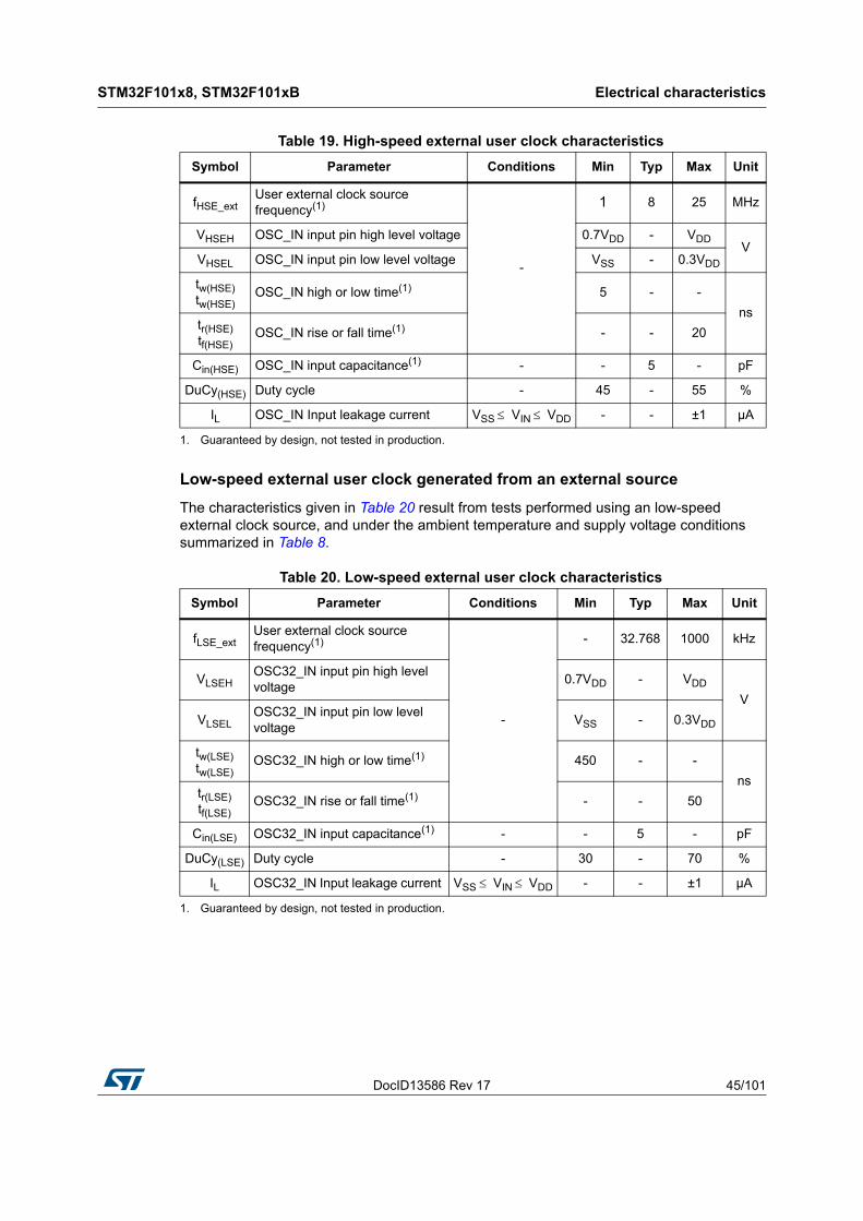
DocID13586 Rev 17 45/101
STM32F101x8, STM32F101xB Electrical characteristics
100
Low-speed external user clock generated from an external source
The characteristics given in Table 20 result from tests performed using an low-speed external clock source, and under the ambient temperature and supply voltage conditions summarized in Table 8.
Table 19. High-speed external user clock characteristics
Symbol Parameter Conditions Min Typ Max Unit
fHSE_extUser external clock source frequency(1)
1. Guaranteed by design, not tested in production.
-
1 8 25 MHz
VHSEH OSC_IN input pin high level voltage 0.7VDD - VDDV
VHSEL OSC_IN input pin low level voltage VSS - 0.3VDD
tw(HSE)tw(HSE)
OSC_IN high or low time(1) 5 - -
nstr(HSE)tf(HSE)
OSC_IN rise or fall time(1) - - 20
Cin(HSE) OSC_IN input capacitance(1) - - 5 - pF
DuCy(HSE) Duty cycle - 45 - 55 %
IL OSC_IN Input leakage current VSS VIN VDD - - ±1 µA
Table 20. Low-speed external user clock characteristics
Symbol Parameter Conditions Min Typ Max Unit
fLSE_extUser external clock source frequency(1)
1. Guaranteed by design, not tested in production.
-
- 32.768 1000 kHz
VLSEHOSC32_IN input pin high level voltage
0.7VDD - VDD
V
VLSELOSC32_IN input pin low level voltage
VSS - 0.3VDD
tw(LSE)tw(LSE)
OSC32_IN high or low time(1) 450 - -
nstr(LSE)tf(LSE)
OSC32_IN rise or fall time(1) - - 50
Cin(LSE) OSC32_IN input capacitance(1) - - 5 - pF
DuCy(LSE) Duty cycle - 30 - 70 %
IL OSC32_IN Input leakage current VSSVIN VDD - - ±1 µA
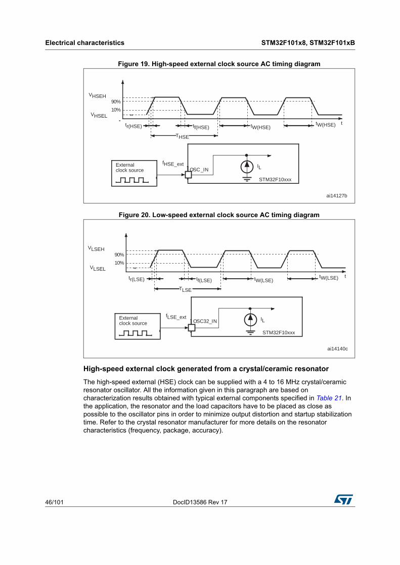
Electrical characteristics STM32F101x8, STM32F101xB
46/101 DocID13586 Rev 17
Figure 19. High-speed external clock source AC timing diagram
Figure 20. Low-speed external clock source AC timing diagram
High-speed external clock generated from a crystal/ceramic resonator
The high-speed external (HSE) clock can be supplied with a 4 to 16 MHz crystal/ceramic resonator oscillator. All the information given in this paragraph are based on characterization results obtained with typical external components specified in Table 21. In the application, the resonator and the load capacitors have to be placed as close as possible to the oscillator pins in order to minimize output distortion and startup stabilization time. Refer to the crystal resonator manufacturer for more details on the resonator characteristics (frequency, package, accuracy).
ai14127b
OSC_INExternal
STM32F10xxx
clock source
VHSEH
tf(HSE) tW(HSE)
IL
90%
10%
THSE
ttr(HSE)tW(HSE)
fHSE_ext
VHSEL
ai14140c
OSC32_INExternal
STM32F10xxx
clock source
VLSEH
tf(LSE) tW(LSE)
IL
90%
10%
TLSE
ttr(LSE)tW(LSE)
fLSE_ext
VLSEL
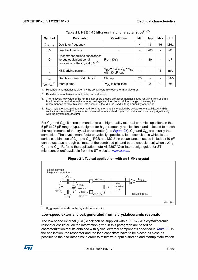
DocID13586 Rev 17 47/101
STM32F101x8, STM32F101xB Electrical characteristics
100
For CL1 and CL2, it is recommended to use high-quality external ceramic capacitors in the 5 pF to 25 pF range (typ.), designed for high-frequency applications, and selected to match the requirements of the crystal or resonator (see Figure 21). CL1 and CL2 are usually the same size. The crystal manufacturer typically specifies a load capacitance which is the series combination of CL1 and CL2. PCB and MCU pin capacitance must be included (10 pF can be used as a rough estimate of the combined pin and board capacitance) when sizing CL1 and CL2. Refer to the application note AN2867 “Oscillator design guide for ST microcontrollers” available from the ST website www.st.com.
Figure 21. Typical application with an 8 MHz crystal
1. REXT value depends on the crystal characteristics.
Low-speed external clock generated from a crystal/ceramic resonator
The low-speed external (LSE) clock can be supplied with a 32.768 kHz crystal/ceramic resonator oscillator. All the information given in this paragraph are based on characterization results obtained with typical external components specified in Table 22. In the application, the resonator and the load capacitors have to be placed as close as possible to the oscillator pins in order to minimize output distortion and startup stabilization
Table 21. HSE 4-16 MHz oscillator characteristics(1)(2)
1. Resonator characteristics given by the crystal/ceramic resonator manufacturer.
2. Based on characterization, not tested in production.
Symbol Parameter Conditions Min Typ Max Unit
fOSC_IN Oscillator frequency - 4 8 16 MHz
RF Feedback resistor - - 200 - k
CRecommended load capacitance versus equivalent serial resistance of the crystal (RS)(3)
3. The relatively low value of the RF resistor offers a good protection against issues resulting from use in a humid environment, due to the induced leakage and the bias condition change. However, it is recommended to take this point into account if the MCU is used in tough humidity conditions.
RS = 30 - 30 - pF
i2 HSE driving currentVDD = 3.3 V, VIN = VSS with 30 pF load
- - 1 mA
gm Oscillator transconductance Startup 25 - - mA/V
tSU(HSE)(4)
4. tSU(HSE) is the startup time measured from the moment it is enabled (by software) to a stabilized 8 MHz oscillation is reached. This value is measured for a standard crystal resonator and it can vary significantly with the crystal manufacturer
Startup time VDD is stabilized - 2 - ms
ai14128b
OSC_OUT
OSC_IN fHSECL1
RF
STM32F10xxx
8 MHzresonator
Resonator withintegrated capacitors
Bias controlled
gain
REXT(1) CL2
Electrical characteristics STM32F101x8, STM32F101xB
48/101 DocID13586 Rev 17
time. Refer to the crystal resonator manufacturer for more details on the resonator characteristics (frequency, package, accuracy).
Note: For CL1 and CL2 it is recommended to use high-quality ceramic capacitors in the 5 pF to 15 pF range selected to match the requirements of the crystal or resonator. CL1 and CL2, are usually the same size. The crystal manufacturer typically specifies a load capacitance which is the series combination of CL1 and CL2.Load capacitance CL has the following formula: CL = CL1 x CL2 / (CL1 + CL2) + Cstray where Cstray is the pin capacitance and board or trace PCB-related capacitance. Typically, it is between 2 pF and 7 pF.
Caution: To avoid exceeding the maximum value of CL1 and CL2 (15 pF) it is strongly recommended to use a resonator with a load capacitance CL 7 pF. Never use a resonator with a load capacitance of 12.5 pF.Example: if resonator with a load capacitance of CL = 6 pF, and Cstray = 2 pF is chosen, then CL1 = CL2 = 8 pF.
Table 22. LSE oscillator characteristics (fLSE = 32.768 kHz)(1) (2)
Symbol Parameter Conditions - Min Typ Max Unit
RF Feedback resistor - - - 5 - M
CRecommended load capacitance versus equivalent serial resistance of the crystal (RS)
RS = 30 K - - - 15 pF
I2 LSE driving currentVDD = 3.3 VVIN = VSS
- - - 1.4 µA
gm Oscillator transconductance - - 5 - - µA/V
tSU(LSE)(3) Startup time
VDD is stabilized
TA = 50 °C - 1.5 -
s
TA = 25 °C - 2.5 -
TA = 10 °C - 4 -
TA = 0 °C - 6 -
TA = -10 °C - 10 -
TA = -20 °C - 17 -
TA = -30 °C - 32 -
TA = -40 °C - 60 -
1. Based on characterization, not tested in production.
2. Refer to the note and caution paragraphs below the table, and to the application note AN2867 “Oscillator design guide for ST microcontrollers”.
3. tSU(LSE) is the startup time measured from the moment it is enabled (by software) to a stabilized 32.768 kHz oscillation is reached. This value is measured for a standard crystal and it can vary significantly with the crystal manufacturer
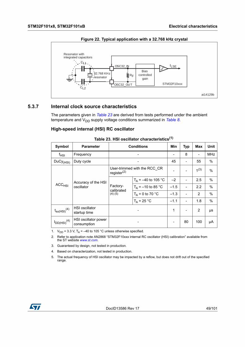
DocID13586 Rev 17 49/101
STM32F101x8, STM32F101xB Electrical characteristics
100
Figure 22. Typical application with a 32.768 kHz crystal
5.3.7 Internal clock source characteristics
The parameters given in Table 23 are derived from tests performed under the ambient temperature and VDD supply voltage conditions summarized in Table 8.
High-speed internal (HSI) RC oscillator
ai14129b
OSC32_OUT
OSC32_IN fLSECL1
RF
STM32F10xxx
32.768 KHzresonator
Resonator withintegrated capacitors
Bias controlled
gain
CL2
Table 23. HSI oscillator characteristics(1)
1. VDD = 3.3 V, TA = –40 to 105 °C unless otherwise specified.
Symbol Parameter Conditions Min Typ Max Unit
fHSI Frequency - - 8 - MHz
DuCy(HSI) Duty cycle - 45 - 55 %
ACCHSIAccuracy of the HSI oscillator
User-trimmed with the RCC_CR register(2)
2. Refer to application note AN2868 “STM32F10xxx internal RC oscillator (HSI) calibration” available from the ST website www.st.com.
- - 1(3)
3. Guaranteed by design, not tested in production.
%
Factory-calibrated(4)
(5)
4. Based on characterization, not tested in production.
5. The actual frequency of HSI oscillator may be impacted by a reflow, but does not drift out of the specified range.
TA = –40 to 105 °C –2 - 2.5 %
TA = –10 to 85 °C –1.5 - 2.2 %
TA = 0 to 70 °C –1.3 - 2 %
TA = 25 °C –1.1 - 1.8 %
tsu(HSI)(4) HSI oscillator
startup time- 1 - 2 µs
IDD(HSI)(4) HSI oscillator power
consumption- - 80 100 µA
Electrical characteristics STM32F101x8, STM32F101xB
50/101 DocID13586 Rev 17
Low-speed internal (LSI) RC oscillator
Wakeup time from low-power mode
The wakeup times given in Table 25 are measured on a wakeup phase with an 8-MHz HSI RC oscillator. The clock source used to wake up the device depends from the current operating mode:
Stop or Standby mode: the clock source is the RC oscillator
Sleep mode: the clock source is the clock that was set before entering Sleep mode.
All timings are derived from tests performed under the ambient temperature and VDD supply voltage conditions summarized in Table 8.
5.3.8 PLL characteristics
The parameters given in Table 26 are derived from tests performed under the ambient temperature and VDD supply voltage conditions summarized in Table 8.
Table 24. LSI oscillator characteristics (1)
1. VDD = 3 V, TA = –40 to 85 °C unless otherwise specified.
Symbol Parameter Min Typ Max Unit
fLSI(2)
2. Based on characterization, not tested in production.
Frequency 30 40 60 kHz
tsu(LSI)(3)
3. Guaranteed by design, not tested in production.
LSI oscillator startup time - - 85 µs
IDD(LSI)(3) LSI oscillator power consumption - 0.65 1.2 µA
Table 25. Low-power mode wakeup timings
Symbol Parameter Typ Unit
tWUSLEEP(1)
1. The wakeup times are measured from the wakeup event to the point at which the user application code reads the first instruction.
Wakeup from Sleep mode 1.8 µs
tWUSTOP(1)
Wakeup from Stop mode (regulator in run mode) 3.6µs
Wakeup from Stop mode (regulator in low-power mode) 5.4
tWUSTDBY(1) Wakeup from Standby mode 50 µs
Table 26. PLL characteristics
Symbol ParameterValue
UnitMin(1) Typ Max(1)
fPLL_IN
PLL input clock(2) 1 8.0 25 MHz
PLL input clock duty cycle 40 - 60 %
fPLL_OUT PLL multiplier output clock 16 - 36 MHz
DocID13586 Rev 17 51/101
STM32F101x8, STM32F101xB Electrical characteristics
100
5.3.9 Memory characteristics
Flash memory
The characteristics are given at TA = –40 to 85 °C unless otherwise specified.
5.3.10 EMC characteristics
Susceptibility tests are performed on a sample basis during device characterization.
Functional EMS (Electromagnetic susceptibility)
While a simple application is executed on the device (toggling 2 LEDs through I/O ports). the device is stressed by two electromagnetic events until a failure occurs. The failure is indicated by the LEDs:
Electrostatic discharge (ESD) (positive and negative) is applied to all device pins until a functional disturbance occurs. This test is compliant with the IEC 61000-4-2 standard.
FTB: A Burst of Fast Transient voltage (positive and negative) is applied to VDD and VSS through a 100 pF capacitor, until a functional disturbance occurs. This test is compliant with the IEC 61000-4-4 standard.
A device reset allows normal operations to be resumed.
tLOCK PLL lock time - - 200 µs
Jitter Cycle-to-cycle jitter - - 300 ps
1. Based on device characterization, not tested in production.
2. Take care of using the appropriate multiplier factors so as to have PLL input clock values compatible with the range defined by fPLL_OUT.
Table 26. PLL characteristics (continued)
Symbol ParameterValue
UnitMin(1) Typ Max(1)
Table 27. Flash memory characteristics
Symbol Parameter Conditions Min(1)
1. Guaranteed by design, not tested in production.
Typ Max(1) Unit
tprog 16-bit programming time TA–40 to +85 °C 40 52.5 70 µs
tERASE Page (1 KB) erase time TA –40 to +85 °C 20 - 40 ms
tME Mass erase time TA –40 to +85 °C 20 - 40 ms
IDD Supply current
Read modefHCLK = 36 MHz with 1 wait state, VDD = 3.3 V
- - 20 mA
Write / Erase modes fHCLK = 36 MHz, VDD = 3.3 V
- - 5 mA
Power-down mode / Halt, VDD = 3.0 to 3.6 V
- - 50 µA
Vprog Programming voltage - 2 - 3.6 V
Electrical characteristics STM32F101x8, STM32F101xB
52/101 DocID13586 Rev 17
The test results are given in Table 28. They are based on the EMS levels and classes defined in application note AN1709.
Designing hardened software to avoid noise problems
EMC characterization and optimization are performed at component level with a typical application environment and simplified MCU software. It should be noted that good EMC performance is highly dependent on the user application and the software in particular.
Therefore it is recommended that the user applies EMC software optimization and pre qualification tests in relation with the EMC level requested for his application.
Software recommendations
The software flowchart must include the management of runaway conditions such as:
Corrupted program counter
Unexpected reset
Critical Data corruption (control registers...)
Prequalification trials
Most of the common failures (unexpected reset and program counter corruption) can be reproduced by manually forcing a low state on the NRST pin or the Oscillator pins for 1 second. To complete these trials, ESD stress can be applied directly on the device, over the range of specification values. When unexpected behavior is detected, the software can be hardened to prevent unrecoverable errors occurring (see application note AN1015).
Electromagnetic Interference (EMI)
The electromagnetic field emitted by the device is monitored while a simple application is executed (toggling 2 LEDs through the I/O ports). This emission test is compliant with IEC61967-2 standard which specifies the test board and the pin loading.
Table 28. EMS characteristics
Symbol Parameter Conditions Level/Class
VFESDVoltage limits to be applied on any I/O pin to induce a functional disturbance
VDD 3.3 V, TA +25 °C, fHCLK 36 MHzconforms to IEC 61000-4-2
2B
VEFTB
Fast transient voltage burst limits to be applied through 100 pF on VDD and VSS pins to induce a functional disturbance
VDD3.3 V, TA +25 °C, fHCLK 36 MHzconforms to IEC 61000-4-4
4A
Table 29. EMI characteristics
Symbol Parameter ConditionsMonitored
frequency band
Max vs. [fHSE/fHCLK]Unit
8/36 MHz
SEMI Peak level
VDD 3.3 V, TA 25 °C, LQFP100 package compliant withIEC 61967-2
0.1 MHz to 30 MHz 7
dBµV30 MHz to 130 MHz 8
130 MHz to 1GHz 13
SAE EMI Level 3.5 -
DocID13586 Rev 17 53/101
STM32F101x8, STM32F101xB Electrical characteristics
100
5.3.11 Absolute maximum ratings (electrical sensitivity)
Based on three different tests (ESD, LU) using specific measurement methods, the device is stressed in order to determine its performance in terms of electrical sensitivity.
Electrostatic discharge (ESD)
Electrostatic discharges (a positive then a negative pulse separated by 1 second) are applied to the pins of each sample according to each pin combination. The sample size depends on the number of supply pins in the device (3 parts × (n+1) supply pins). This test conforms to the JESD22-A114/C101 standard.
Static latch-up
Two complementary static tests are required on six parts to assess the latch-up performance:
A supply overvoltage is applied to each power supply pin
A current injection is applied to each input, output and configurable I/O pin
These tests are compliant with EIA/JESD 78 IC latch-up standard.
5.3.12 I/O current injection characteristics
As a general rule, current injection to the I/O pins, due to external voltage below VSS or above VDD (for standard, 3 V-capable I/O pins) should be avoided during normal product operation. However, in order to give an indication of the robustness of the microcontroller in cases when abnormal injection accidentally happens, susceptibility tests are performed on a sample basis during device characterization.
Functional susceptibilty to I/O current injection
While a simple application is executed on the device, the device is stressed by injecting current into the I/O pins programmed in floating input mode. While current is injected into the I/O pin, one at a time, the device is checked for functional failures.
Table 30. ESD absolute maximum ratings
Symbol Ratings Conditions ClassMaximum value(1)
1. Based on characterization results, not tested in production.
Unit
VESD(HBM)Electrostatic discharge voltage (human body model)
TA +25 °Cconforming to JESD22-A114
2 2000
V
VESD(CDM)Electrostatic discharge voltage (charge device model)
TA +25 °Cconforming to ANSI/ESD STM5.3.1
II 500
Table 31. Electrical sensitivities
Symbol Parameter Conditions Class
LU Static latch-up class TA +85 °C conforming to JESD78A II level A
Electrical characteristics STM32F101x8, STM32F101xB
54/101 DocID13586 Rev 17
The failure is indicated by an out of range parameter: ADC error above a certain limit (>5 LSB TUE), out of spec current injection on adjacent pins or other functional failure (for example reset, oscillator frequency deviation).
The test results are given in Table 32
Table 32. I/O current injection susceptibility
Symbol Description
Functional susceptibility
UnitNegative injection
Positive injection
IINJ
Injected current on OSC_IN32, OSC_OUT32, PA4, PA5, PC13
-0 +0
mAInjected current on all FT pins -5 +0
Injected current on any other pin -5 +5
DocID13586 Rev 17 55/101
STM32F101x8, STM32F101xB Electrical characteristics
100
5.3.13 I/O port characteristics
General input/output characteristics
Unless otherwise specified, the parameters given in Table 33 are derived from tests performed under the conditions summarized in Table 8. All I/Os are CMOS and TTL compliant.
Table 33. I/O static characteristics
Symbol Parameter Conditions Min Typ Max Unit
VILLow level input voltage
Standard IO input low level voltage
- - 0.28*(VDD-2 V)+0.8 V(1)
V
IO FT(3) input low level voltage
- - 0.32*(VDD-2 V)+0.75 V(1)
All I/Os except BOOT0
- - 0.35VDD(2)
VIHHigh level input voltage
Standard IO input high level voltage
0.41*(VDD-2 V)+1.3 V(1) - -
IO FT(3) input high level voltage
0.42*(VDD-2 V)+1 V(1) - -
All I/Os except BOOT0
0.65VDD(2) - -
Vhys
Standard IO Schmitt trigger voltage hysteresis(4)
- 200 - -
mV
IO FT Schmitt trigger voltage hysteresis(4) - 5% VDD
(5) - -
IlkgInput leakage current (6)
VSS VIN VDDStandard I/Os
- - 1
µAVIN = 5 VI/O FT
- - 3
RPUWeak pull-up equivalent resistor(7) VIN VSS 30 40 50
k
RPDWeak pull-down equivalent resistor(7) VIN VDD 30 40 50
CIO I/O pin capacitance - - 5 - pF
1. Data based on design simulation.
2. Tested in production.
3. FT = Five-volt tolerant. In order to sustain a voltage higher than VDD+0.3 the internal pull-up/pull-down resistors must be disabled.
4. Hysteresis voltage between Schmitt trigger switching levels. Based on characterization, not tested in production.
5. With a minimum of 100 mV.
6. Leakage could be higher than max. if negative current is injected on adjacent pins.
7. Pull-up and pull-down resistors are designed with a true resistance in series with a switchable PMOS/NMOS. This PMOS/NMOS contribution to the series resistance is minimum (~10% order).
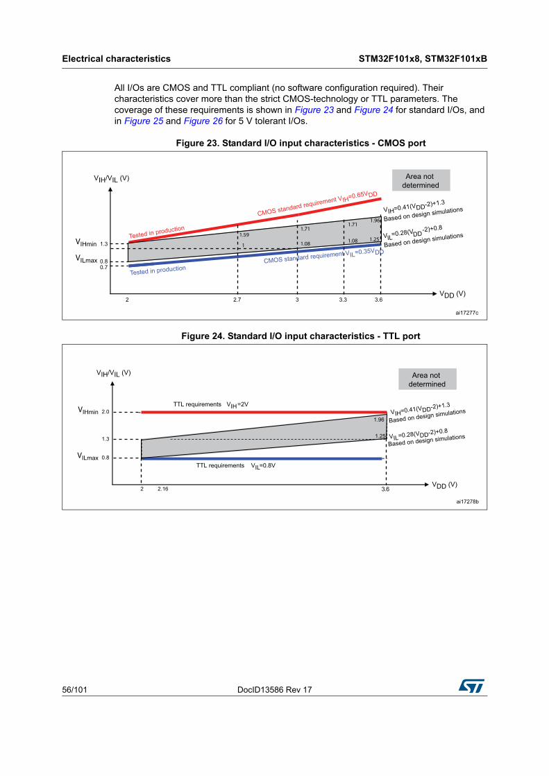
Electrical characteristics STM32F101x8, STM32F101xB
56/101 DocID13586 Rev 17
All I/Os are CMOS and TTL compliant (no software configuration required). Their characteristics cover more than the strict CMOS-technology or TTL parameters. The coverage of these requirements is shown in Figure 23 and Figure 24 for standard I/Os, and in Figure 25 and Figure 26 for 5 V tolerant I/Os.
Figure 23. Standard I/O input characteristics - CMOS port
Figure 24. Standard I/O input characteristics - TTL port
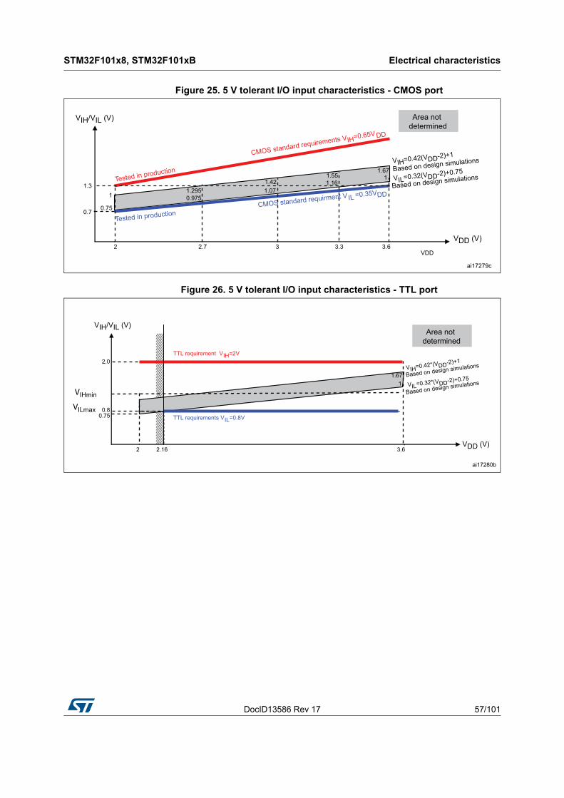
DocID13586 Rev 17 57/101
STM32F101x8, STM32F101xB Electrical characteristics
100
Figure 25. 5 V tolerant I/O input characteristics - CMOS port
Figure 26. 5 V tolerant I/O input characteristics - TTL port
Electrical characteristics STM32F101x8, STM32F101xB
58/101 DocID13586 Rev 17
Output driving current
The GPIOs (general-purpose inputs/outputs) can sink or source up to ±8 mA, and sink or source up to ±20 mA (with a relaxed VOL/VOH) except PC13, PC14 and PC15 which can sink or source up to +/-3mA. When using the GPIOs PC13 to PC15 in output mode, the speed should not exceed 2 MHz with a maximum load of 30 pF.
In the user application, the number of I/O pins which can drive current must be limited to respect the absolute maximum rating specified in Section 5.2:
The sum of the currents sourced by all the I/Os on VDD, plus the maximum Run consumption of the MCU sourced on VDD, cannot exceed the absolute maximum rating IVDD (see Table 6).
The sum of the currents sunk by all the I/Os on VSS plus the maximum Run consumption of the MCU sunk on VSS cannot exceed the absolute maximum rating IVSS (see Table 6).
Output voltage levels
Unless otherwise specified, the parameters given in Table 34 are derived from tests performed under the ambient temperature and VDD supply voltage conditions summarized in Table 8. All I/Os are CMOS and TTL compliant.
Table 34. Output voltage characteristics
Symbol Parameter Conditions Min Max Unit
VOL(1)
1. The IIO current sunk by the device must always respect the absolute maximum rating specified in Table 6 and the sum of IIO (I/O ports and control pins) must not exceed IVSS.
Output Low level voltage for an I/O pin when 8 pins are sunk at the same time CMOS port(2),,
IIO = +8 mA,2.7 V < VDD < 3.6 V
2. TTL and CMOS outputs are compatible with JEDEC standards JESD36 and JESD52.
- 0.4
V
VOH(3)
3. The IIO current sourced by the device must always respect the absolute maximum rating specified in Table 6 and the sum of IIO (I/O ports and control pins) must not exceed IVDD.
Output High level voltage for an I/O pin when 8 pins are sourced at the same time
VDD–0.4 -
VOL(1) Output low level voltage for an I/O pin
when 8 pins are sunk at the same time TTL port(2)
IIO = +8 mA
2.7 V < VDD < 3.6 V
- 0.4
V
VOH(3) Output high level voltage for an I/O pin
when 8 pins are sourced at the same time2.4 -
VOL(1) Output low level voltage for an I/O pin
when 8 pins are sunk at the same time IIO = +20 mA(4)
2.7 V < VDD < 3.6 V
4. Based on characterization data, not tested in production.
- 1.3
V
VOH (3) Output high level voltage for an I/O pin
when 8 pins are sourced at the same time VDD–1.3 -
VOL(1) Output low level voltage for an I/O pin
when 8 pins are sunk at the same time IIO = +6 mA(4)
2 V < VDD < 2.7 V
- 0.4
V
VOH(3) Output high level voltage for an I/O pin
when 8 pins are sourced at the same time VDD–0.4 -
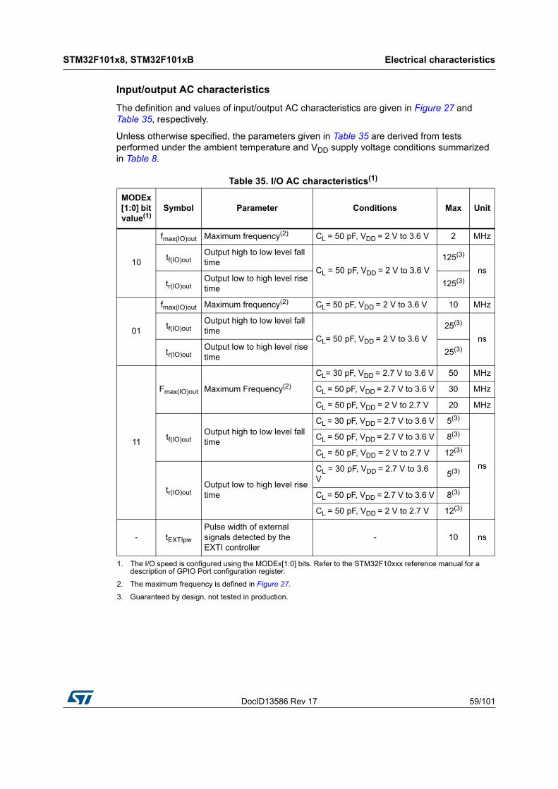
DocID13586 Rev 17 59/101
STM32F101x8, STM32F101xB Electrical characteristics
100
Input/output AC characteristics
The definition and values of input/output AC characteristics are given in Figure 27 and Table 35, respectively.
Unless otherwise specified, the parameters given in Table 35 are derived from tests performed under the ambient temperature and VDD supply voltage conditions summarized in Table 8.
Table 35. I/O AC characteristics(1)
1. The I/O speed is configured using the MODEx[1:0] bits. Refer to the STM32F10xxx reference manual for a description of GPIO Port configuration register.
MODEx[1:0] bit value(1)
Symbol Parameter Conditions Max Unit
10
fmax(IO)out Maximum frequency(2)
2. The maximum frequency is defined in Figure 27.
CL = 50 pF, VDD = 2 V to 3.6 V 2 MHz
tf(IO)outOutput high to low level fall time
CL = 50 pF, VDD = 2 V to 3.6 V
125(3)
3. Guaranteed by design, not tested in production.
ns
tr(IO)outOutput low to high level rise time
125(3)
01
fmax(IO)out Maximum frequency(2) CL= 50 pF, VDD = 2 V to 3.6 V 10 MHz
tf(IO)outOutput high to low level fall time
CL= 50 pF, VDD = 2 V to 3.6 V
25(3)
ns
tr(IO)outOutput low to high level rise time
25(3)
11
Fmax(IO)out Maximum Frequency(2)
CL= 30 pF, VDD = 2.7 V to 3.6 V 50 MHz
CL = 50 pF, VDD = 2.7 V to 3.6 V 30 MHz
CL = 50 pF, VDD = 2 V to 2.7 V 20 MHz
tf(IO)outOutput high to low level fall time
CL = 30 pF, VDD = 2.7 V to 3.6 V 5(3)
ns
CL = 50 pF, VDD = 2.7 V to 3.6 V 8(3)
CL = 50 pF, VDD = 2 V to 2.7 V 12(3)
tr(IO)outOutput low to high level rise time
CL = 30 pF, VDD = 2.7 V to 3.6 V
5(3)
CL = 50 pF, VDD = 2.7 V to 3.6 V 8(3)
CL = 50 pF, VDD = 2 V to 2.7 V 12(3)
- tEXTIpw
Pulse width of external signals detected by the EXTI controller
- 10 ns
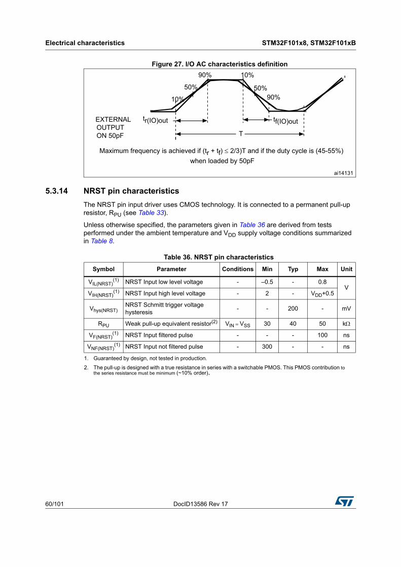
Electrical characteristics STM32F101x8, STM32F101xB
60/101 DocID13586 Rev 17
Figure 27. I/O AC characteristics definition
5.3.14 NRST pin characteristics
The NRST pin input driver uses CMOS technology. It is connected to a permanent pull-up resistor, RPU (see Table 33).
Unless otherwise specified, the parameters given in Table 36 are derived from tests performed under the ambient temperature and VDD supply voltage conditions summarized in Table 8.
Table 36. NRST pin characteristics
Symbol Parameter Conditions Min Typ Max Unit
VIL(NRST)(1)
1. Guaranteed by design, not tested in production.
NRST Input low level voltage - –0.5 - 0.8V
VIH(NRST)(1) NRST Input high level voltage - 2 - VDD+0.5
Vhys(NRST)NRST Schmitt trigger voltage hysteresis
- - 200 - mV
RPU Weak pull-up equivalent resistor(2)
2. The pull-up is designed with a true resistance in series with a switchable PMOS. This PMOS contribution to the series resistance must be minimum (~10% order).
VIN VSS 30 40 50 k
VF(NRST)(1) NRST Input filtered pulse - - - 100 ns
VNF(NRST)(1) NRST Input not filtered pulse - 300 - - ns
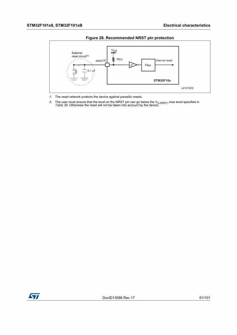
DocID13586 Rev 17 61/101
STM32F101x8, STM32F101xB Electrical characteristics
100
Figure 28. Recommended NRST pin protection
1. The reset network protects the device against parasitic resets.
2. The user must ensure that the level on the NRST pin can go below the VIL(NRST) max level specified in Table 36. Otherwise the reset will not be taken into account by the device.
ai14132d
STM32F10x
RPUNRST(2)
VDD
Filter
Internal reset
0.1 µF
Externalreset circuit(1)
Electrical characteristics STM32F101x8, STM32F101xB
62/101 DocID13586 Rev 17
5.3.15 TIM timer characteristics
The parameters given in Table 37 are guaranteed by design.
Refer to Section 5.3.12: I/O current injection characteristics for details on the input/output alternate function characteristics (output compare, input capture, external clock, PWM output).
5.3.16 Communications interfaces
I2C interface characteristics
The STM32F101xx medium-density access line I2C interface meets the requirements of the standard I2C communication protocol with the following restrictions: the I/O pins SDA and SCL are mapped to are not “true” open-drain. When configured as open-drain, the PMOS connected between the I/O pin and VDD is disabled, but is still present.
The I2C characteristics are described in Table 38. Refer also to Section 5.3.12: I/O current injection characteristics for more details on the input/output alternate function characteristics (SDA and SCL).
Table 37. TIMx(1) characteristics
1. TIMx is used as a general term to refer to the TIM1, TIM2, TIM3 and TIM4 timers.
Symbol Parameter Conditions Min Max Unit
tres(TIM) Timer resolution time- 1 - tTIMxCLK
fTIMxCLK = 36 MHz 27.8 - ns
fEXTTimer external clock frequency on CH1 to CH4
0 fTIMxCLK/2 MHz
fTIMxCLK = 36 MHz 0 18 MHz
ResTIM Timer resolution - - 16 bit
tCOUNTER
16-bit counter clock period when internal clock is selected
- 1 65536 tTIMxCLK
fTIMxCLK = 36 MHz 0.0278 1820 µs
tMAX_COUNT Maximum possible count- - 65536 × 65536 tTIMxCLK
fTIMxCLK = 36 MHz - 119.2 s
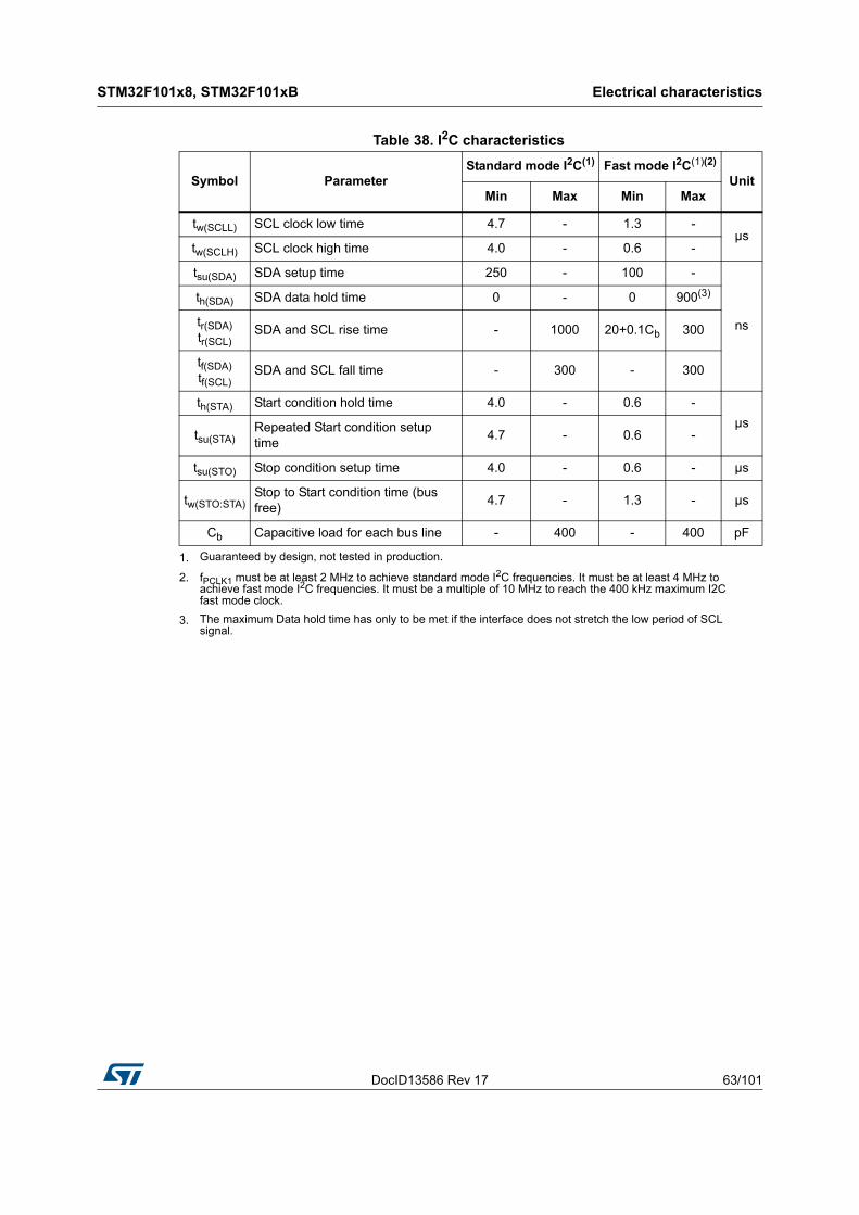
DocID13586 Rev 17 63/101
STM32F101x8, STM32F101xB Electrical characteristics
100
Table 38. I2C characteristics
Symbol ParameterStandard mode I2C(1)
1. Guaranteed by design, not tested in production.
Fast mode I2C(1)(2)
2. fPCLK1 must be at least 2 MHz to achieve standard mode I2C frequencies. It must be at least 4 MHz to achieve fast mode I2C frequencies. It must be a multiple of 10 MHz to reach the 400 kHz maximum I2C fast mode clock.
UnitMin Max Min Max
tw(SCLL) SCL clock low time 4.7 - 1.3 -µs
tw(SCLH) SCL clock high time 4.0 - 0.6 -
tsu(SDA) SDA setup time 250 - 100 -
ns
th(SDA) SDA data hold time 0 - 0 900(3)
3. The maximum Data hold time has only to be met if the interface does not stretch the low period of SCL signal.
tr(SDA)tr(SCL)
SDA and SCL rise time - 1000 20+0.1Cb 300
tf(SDA)tf(SCL)
SDA and SCL fall time - 300 - 300
th(STA) Start condition hold time 4.0 - 0.6 -
µstsu(STA)
Repeated Start condition setup time
4.7 - 0.6 -
tsu(STO) Stop condition setup time 4.0 - 0.6 - µs
tw(STO:STA)Stop to Start condition time (bus free)
4.7 - 1.3 - µs
Cb Capacitive load for each bus line - 400 - 400 pF
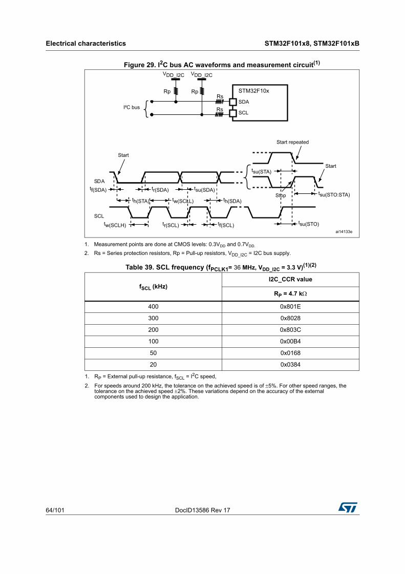
Electrical characteristics STM32F101x8, STM32F101xB
64/101 DocID13586 Rev 17
Figure 29. I2C bus AC waveforms and measurement circuit(1)
1. Measurement points are done at CMOS levels: 0.3VDD and 0.7VDD.
2. Rs = Series protection resistors, Rp = Pull-up resistors, VDD_I2C = I2C bus supply.
Table 39. SCL frequency (fPCLK1= 36 MHz, VDD_I2C = 3.3 V)(1)(2)
1. RP = External pull-up resistance, fSCL = I2C speed,
2. For speeds around 200 kHz, the tolerance on the achieved speed is of 5%. For other speed ranges, the tolerance on the achieved speed 2%. These variations depend on the accuracy of the external components used to design the application.
fSCL (kHz)I2C_CCR value
RP = 4.7 k
400 0x801E
300 0x8028
200 0x803C
100 0x00B4
50 0x0168
20 0x0384
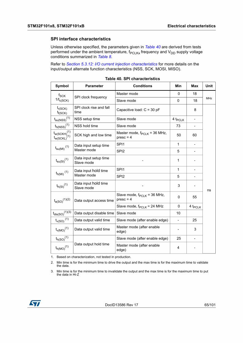
DocID13586 Rev 17 65/101
STM32F101x8, STM32F101xB Electrical characteristics
100
SPI interface characteristics
Unless otherwise specified, the parameters given in Table 40 are derived from tests performed under the ambient temperature, fPCLKx frequency and VDD supply voltage conditions summarized in Table 8.
Refer to Section 5.3.12: I/O current injection characteristics for more details on the input/output alternate function characteristics (NSS, SCK, MOSI, MISO).
Table 40. SPI characteristics
Symbol Parameter Conditions Min Max Unit
fSCK1/tc(SCK)
SPI clock frequencyMaster mode 0 18
MHzSlave mode 0 18
tr(SCK)tf(SCK)
SPI clock rise and fall time
Capacitive load: C = 30 pF 8
ns
tsu(NSS)(1)
1. Based on characterization, not tested in production.
NSS setup time Slave mode 4 tPCLK -
th(NSS)(1) NSS hold time Slave mode 73 -
tw(SCKH)(1)
tw(SCKL)(1) SCK high and low time
Master mode, fPCLK = 36 MHz, presc = 4
50 60
tsu(MI) (1) Data input setup time
Master mode
SPI1 1 -
SPI2 5 -
tsu(SI)(1) Data input setup time
Slave mode- 1 -
th(MI) (1) Data input hold time
Master mode
SPI1 1 -
SPI2 5 -
th(SI)(1) Data input hold time
Slave mode- 3 -
ta(SO)(1)(2)
2. Min time is for the minimum time to drive the output and the max time is for the maximum time to validate the data.
Data output access time
Slave mode, fPCLK = 36 MHz, presc = 4
0 55
Slave mode, fPCLK = 24 MHz 0 4 tPCLK
tdis(SO)(1)(3)
3. Min time is for the minimum time to invalidate the output and the max time is for the maximum time to put the data in Hi-Z
Data output disable time Slave mode 10
tv(SO) (1) Data output valid time Slave mode (after enable edge) - 25
tv(MO)(1) Data output valid time
Master mode (after enable edge)
- 3
th(SO)(1)
Data output hold time
Slave mode (after enable edge) 25 -
th(MO)(1) Master mode (after enable
edge)4 -
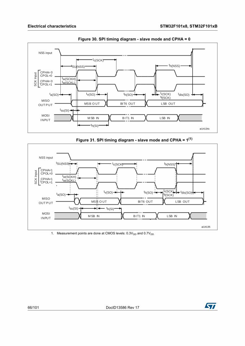
Electrical characteristics STM32F101x8, STM32F101xB
66/101 DocID13586 Rev 17
Figure 30. SPI timing diagram - slave mode and CPHA = 0
Figure 31. SPI timing diagram - slave mode and CPHA = 1(1)
1. Measurement points are done at CMOS levels: 0.3VDD and 0.7VDD.
ai14134c
SC
K In
put CPHA=0
MOSI
INPUT
MISOOUT PUT
CPHA=0
MSB O UT
M SB IN
BIT6 OUT
LSB IN
LSB OUT
CPOL=0
CPOL=1
BIT1 IN
NSS input
tSU(NSS)
tc(SCK)
th(NSS)
ta(SO)
tw(SCKH)tw(SCKL)
tv(SO) th(SO) tr(SCK)tf(SCK)
tdis(SO)
tsu(SI)
th(SI)
ai14135
SC
K In
put CPHA=1
MOSI
INPUT
MISOOUT PUT
CPHA=1
MSB O UT
M SB IN
BIT6 OUT
LSB IN
LSB OUT
CPOL=0
CPOL=1
BIT1 IN
tSU(NSS) tc(SCK) th(NSS)
ta(SO)
tw(SCKH)tw(SCKL)
tv(SO) th(SO)tr(SCK)tf(SCK)
tdis(SO)
tsu(SI) th(SI)
NSS input
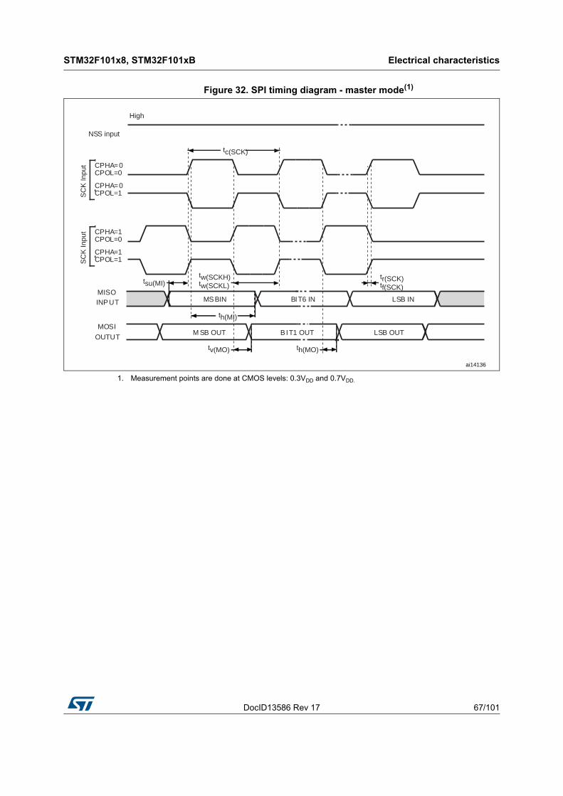
DocID13586 Rev 17 67/101
STM32F101x8, STM32F101xB Electrical characteristics
100
Figure 32. SPI timing diagram - master mode(1)
1. Measurement points are done at CMOS levels: 0.3VDD and 0.7VDD.
ai14136
SC
K In
put CPHA=0
MOSI
OUTUT
MISOINPUT
CPHA=0
MSBIN
M SB OUT
BIT6 IN
LSB OUT
LSB IN
CPOL=0
CPOL=1
BIT1 OUT
NSS input
tc(SCK)
tw(SCKH)tw(SCKL)
tr(SCK)tf(SCK)
th(MI)
High
SC
K In
put CPHA=1
CPHA=1
CPOL=0
CPOL=1
tsu(MI)
tv(MO) th(MO)
Electrical characteristics STM32F101x8, STM32F101xB
68/101 DocID13586 Rev 17
5.3.17 12-bit ADC characteristics
Unless otherwise specified, the parameters given in Table 41 are derived from tests performed under the ambient temperature, fPCLK2 frequency and VDDA supply voltage conditions summarized in Table 8.
Note: It is recommended to perform a calibration after each power-up.
Table 41. ADC characteristics
Symbol Parameter Conditions Min Typ Max Unit
VDDA Power supply - 2.4 - 3.6 V
VREF+ Positive reference voltage - 2.4 - VDDA V
IVREFCurrent on the VREF input pin
- - 160(1) 220(1) µA
fADC ADC clock frequency - 0.6 - 14 MHz
fS(2) Sampling rate - 0.05 - 1 MHz
fTRIG(2) External trigger frequency
fADC = 14 MHz - - 823 kHz
- - - 17 1/fADC
VAIN Conversion voltage range(3) -0 (VSSA or VREF- tied to ground)
- VREF+ V
RAIN(2) External input impedance
See Equation 1 and Table 42 for details
- - 50
RADC(2) Sampling switch resistance - - - 1
CADC(2) Internal sample and hold
capacitor- - - 8 pF
tCAL(2) Calibration time
fADC = 14 MHz 5.9 µs
- 83 1/fADC
tlat(2) Injection trigger conversion
latency
fADC = 14 MHz - - 0.214 µs
- - - 3(4) 1/fADC
tlatr(2) Regular trigger conversion
latency
fADC = 14 MHz - - 0.143 µs
- - - 2(4) 1/fADC
tS(2) Sampling time fADC = 14 MHz
0.107 - 17.1 µs
1.5 - 239.5 1/fADC
tSTAB(2) Power-up time - 0 0 1 µs
tCONV(2) Total conversion time
(including sampling time)
fADC = 14 MHz 1 - 18 µs
-14 to 252 (tS for sampling +12.5 for successive approximation)
1/fADC
1. Based on characterization results, not tested in production.
2. Guaranteed by design, not tested in production.
3. VREF+ can be internally connected to VDDA and VREF- can be internally connected to VSSA, depending on the package. Refer to Section 3: Pinouts and pin description for further details.
4. For external triggers, a delay of 1/fPCLK2 must be added to the latency specified in Table 41.
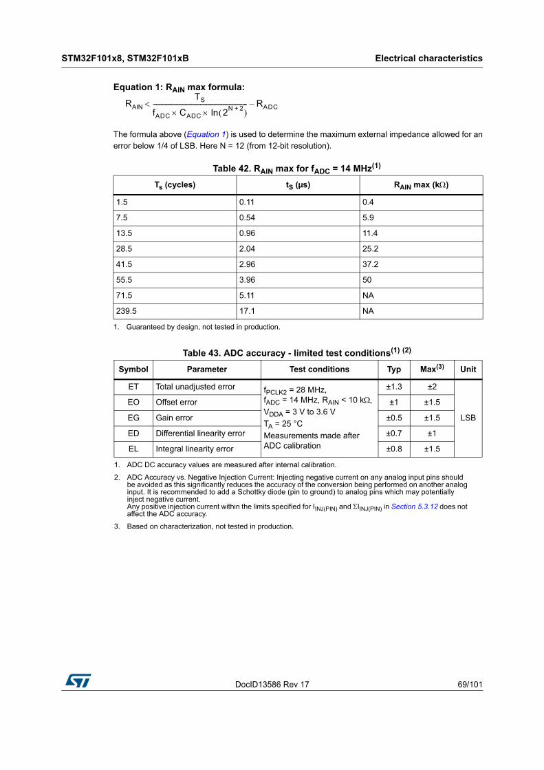
DocID13586 Rev 17 69/101
STM32F101x8, STM32F101xB Electrical characteristics
100
Equation 1: RAIN max formula:
The formula above (Equation 1) is used to determine the maximum external impedance allowed for an error below 1/4 of LSB. Here N = 12 (from 12-bit resolution).
Table 42. RAIN max for fADC = 14 MHz(1)
1. Guaranteed by design, not tested in production.
Ts (cycles) tS (µs) RAIN max (k)
1.5 0.11 0.4
7.5 0.54 5.9
13.5 0.96 11.4
28.5 2.04 25.2
41.5 2.96 37.2
55.5 3.96 50
71.5 5.11 NA
239.5 17.1 NA
Table 43. ADC accuracy - limited test conditions(1) (2)
1. ADC DC accuracy values are measured after internal calibration.
2. ADC Accuracy vs. Negative Injection Current: Injecting negative current on any analog input pins should be avoided as this significantly reduces the accuracy of the conversion being performed on another analog input. It is recommended to add a Schottky diode (pin to ground) to analog pins which may potentially inject negative current. Any positive injection current within the limits specified for IINJ(PIN) and IINJ(PIN) in Section 5.3.12 does not affect the ADC accuracy.
Symbol Parameter Test conditions Typ Max(3)
3. Based on characterization, not tested in production.
Unit
ET Total unadjusted error fPCLK2 = 28 MHz,fADC = 14 MHz, RAIN < 10 k,
VDDA = 3 V to 3.6 V
TA = 25 °C
Measurements made after ADC calibration
±1.3 ±2
LSB
EO Offset error ±1 ±1.5
EG Gain error ±0.5 ±1.5
ED Differential linearity error ±0.7 ±1
EL Integral linearity error ±0.8 ±1.5
RAIN
TS
fADC CADC 2N 2+ ln
-------------------------------------------------------------- RADC–
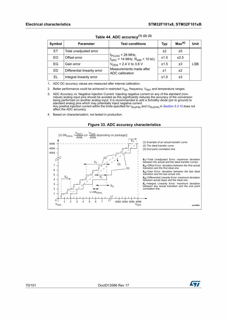
Electrical characteristics STM32F101x8, STM32F101xB
70/101 DocID13586 Rev 17
Figure 33. ADC accuracy characteristics
Table 44. ADC accuracy(1) (2) (3)
1. ADC DC accuracy values are measured after internal calibration.
2. Better performance could be achieved in restricted VDD, frequency, VREF and temperature ranges.
3. ADC Accuracy vs. Negative Injection Current: Injecting negative current on any of the standard (non-robust) analog input pins should be avoided as this significantly reduces the accuracy of the conversion being performed on another analog input. It is recommended to add a Schottky diode (pin to ground) to standard analog pins which may potentially inject negative current. Any positive injection current within the limits specified for IINJ(PIN) and IINJ(PIN) in Section 5.3.12 does not affect the ADC accuracy.
Symbol Parameter Test conditions Typ Max(4)
4. Based on characterization, not tested in production.
Unit
ET Total unadjusted errorfPCLK2 = 28 MHz,fADC = 14 MHz, RAIN < 10 k,
VDDA = 2.4 V to 3.6 V
Measurements made after ADC calibration
±2 ±5
LSB
EO Offset error ±1.5 ±2.5
EG Gain error ±1.5 ±3
ED Differential linearity error ±1 ±2
EL Integral linearity error ±1.5 ±3
EO
EG
1 LSBIDEAL
(1) Example of an actual transfer curve(2) The ideal transfer curve(3) End point correlation line
ET=Total Unadjusted Error: maximum deviationbetween the actual and the ideal transfer curves.EO=Offset Error: deviation between the first actualtransition and the first ideal one.EG=Gain Error: deviation between the last idealtransition and the last actual one.ED=Differential Linearity Error: maximum deviationbetween actual steps and the ideal one.EL=Integral Linearity Error: maximum deviationbetween any actual transition and the end pointcorrelation line.
4095
4094
4093
5
4
3
2
1
0
7
6
1 2 3 4 5 6 7 4093 4094 4095 4096
(1)
(2)
ET
ED
EL
(3)
VDDAVSSA ai14395b
VREF+
4096(or depending on package)]
VDDA
4096[1LSBIDEAL =
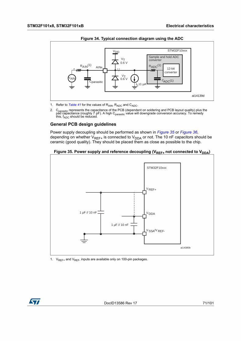
DocID13586 Rev 17 71/101
STM32F101x8, STM32F101xB Electrical characteristics
100
Figure 34. Typical connection diagram using the ADC
1. Refer to Table 41 for the values of RAIN, RADC and CADC.
2. Cparasitic represents the capacitance of the PCB (dependent on soldering and PCB layout quality) plus the pad capacitance (roughly 7 pF). A high Cparasitic value will downgrade conversion accuracy. To remedy this, fADC should be reduced.
General PCB design guidelines
Power supply decoupling should be performed as shown in Figure 35 or Figure 36, depending on whether VREF+ is connected to VDDA or not. The 10 nF capacitors should be ceramic (good quality). They should be placed them as close as possible to the chip.
Figure 35. Power supply and reference decoupling (VREF+ not connected to VDDA)
1. VREF+ and VREF- inputs are available only on 100-pin packages.
ai14139d
STM32F10xxxVDD
AINx
IL±1 µA
0.6 VVT
RAIN(1)
CparasiticVAIN
0.6 VVT
RADC(1)
CADC(1)
12-bitconverter
Sample and hold ADCconverter
VREF+
STM32F10xxx
VDDA
VSSA/V REF-
1 µF // 10 nF
1 µF // 10 nF
ai14380b
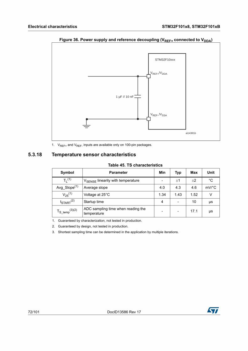
Electrical characteristics STM32F101x8, STM32F101xB
72/101 DocID13586 Rev 17
Figure 36. Power supply and reference decoupling (VREF+ connected to VDDA)
1. VREF+ and VREF- inputs are available only on 100-pin packages.
5.3.18 Temperature sensor characteristics
VREF+/VDDA
STM32F10xxx
1 µF // 10 nF
VREF–/VSSA
ai14381b
Table 45. TS characteristics
Symbol Parameter Min Typ Max Unit
TL(1)
1. Guaranteed by characterization, not tested in production.
VSENSE linearity with temperature - 1 2 °C
Avg_Slope(1) Average slope 4.0 4.3 4.6 mV/°C
V25(1) Voltage at 25°C 1.34 1.43 1.52 V
tSTART(2)
2. Guaranteed by design, not tested in production.
Startup time 4 - 10 µs
TS_temp(3)(2)
3. Shortest sampling time can be determined in the application by multiple iterations.
ADC sampling time when reading the temperature
- - 17.1 µs
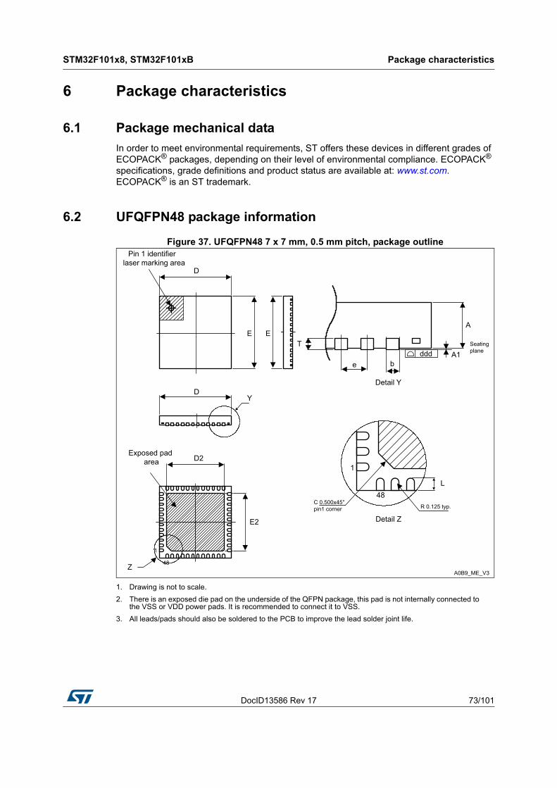
DocID13586 Rev 17 73/101
STM32F101x8, STM32F101xB Package characteristics
100
6 Package characteristics
6.1 Package mechanical data
In order to meet environmental requirements, ST offers these devices in different grades of ECOPACK® packages, depending on their level of environmental compliance. ECOPACK® specifications, grade definitions and product status are available at: www.st.com. ECOPACK® is an ST trademark.
6.2 UFQFPN48 package information
Figure 37. UFQFPN48 7 x 7 mm, 0.5 mm pitch, package outline
1. Drawing is not to scale.
2. There is an exposed die pad on the underside of the QFPN package, this pad is not internally connected to the VSS or VDD power pads. It is recommended to connect it to VSS.
3. All leads/pads should also be soldered to the PCB to improve the lead solder joint life.
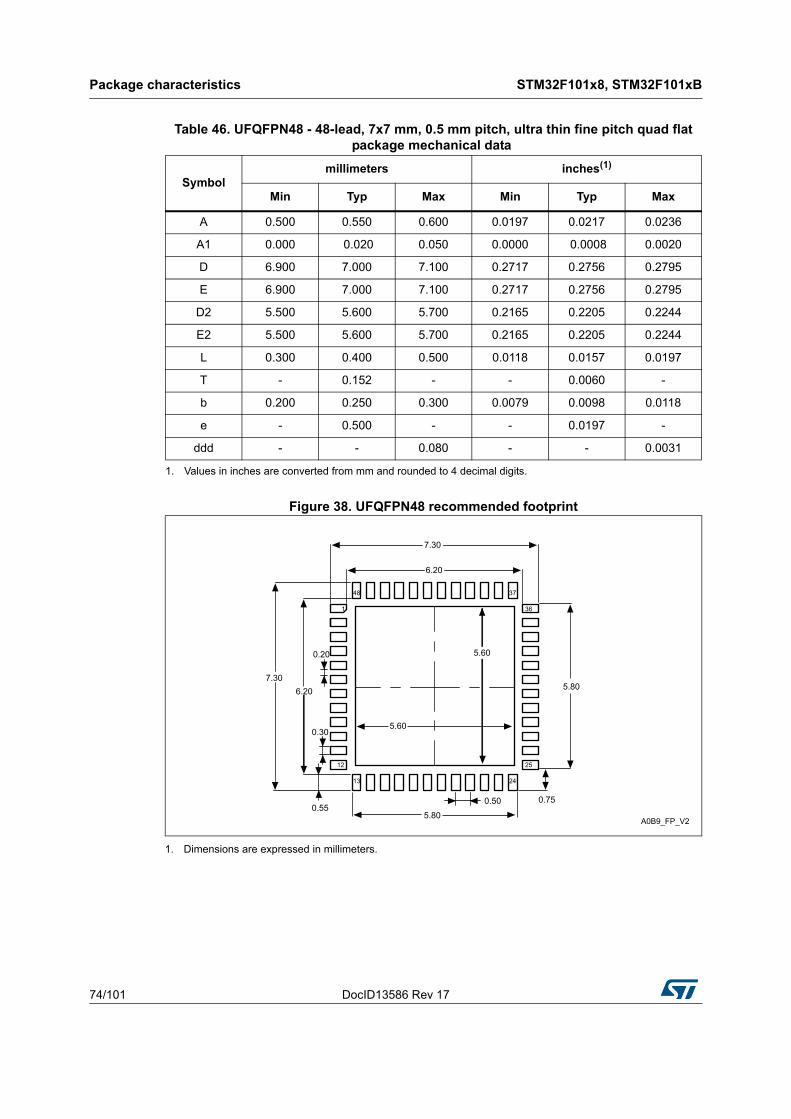
Package characteristics STM32F101x8, STM32F101xB
74/101 DocID13586 Rev 17
Figure 38. UFQFPN48 recommended footprint
1. Dimensions are expressed in millimeters.
Table 46. UFQFPN48 - 48-lead, 7x7 mm, 0.5 mm pitch, ultra thin fine pitch quad flat package mechanical data
Symbolmillimeters inches(1)
1. Values in inches are converted from mm and rounded to 4 decimal digits.
Min Typ Max Min Typ Max
A 0.500 0.550 0.600 0.0197 0.0217 0.0236
A1 0.000 0.020 0.050 0.0000 0.0008 0.0020
D 6.900 7.000 7.100 0.2717 0.2756 0.2795
E 6.900 7.000 7.100 0.2717 0.2756 0.2795
D2 5.500 5.600 5.700 0.2165 0.2205 0.2244
E2 5.500 5.600 5.700 0.2165 0.2205 0.2244
L 0.300 0.400 0.500 0.0118 0.0157 0.0197
T - 0.152 - - 0.0060 -
b 0.200 0.250 0.300 0.0079 0.0098 0.0118
e - 0.500 - - 0.0197 -
ddd - - 0.080 - - 0.0031
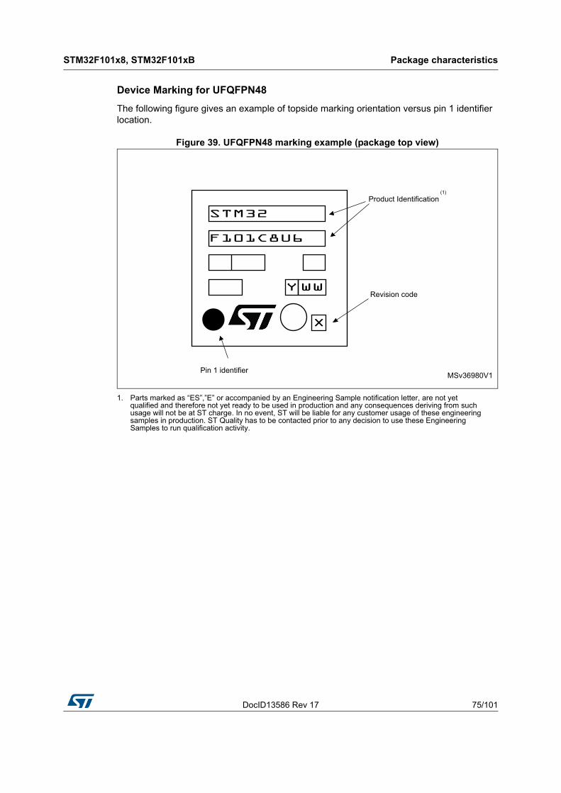
DocID13586 Rev 17 75/101
STM32F101x8, STM32F101xB Package characteristics
100
Device Marking for UFQFPN48
The following figure gives an example of topside marking orientation versus pin 1 identifier location.
Figure 39. UFQFPN48 marking example (package top view)
1. Parts marked as “ES”,”E” or accompanied by an Engineering Sample notification letter, are not yet qualified and therefore not yet ready to be used in production and any consequences deriving from such usage will not be at ST charge. In no event, ST will be liable for any customer usage of these engineering samples in production. ST Quality has to be contacted prior to any decision to use these Engineering Samples to run qualification activity.
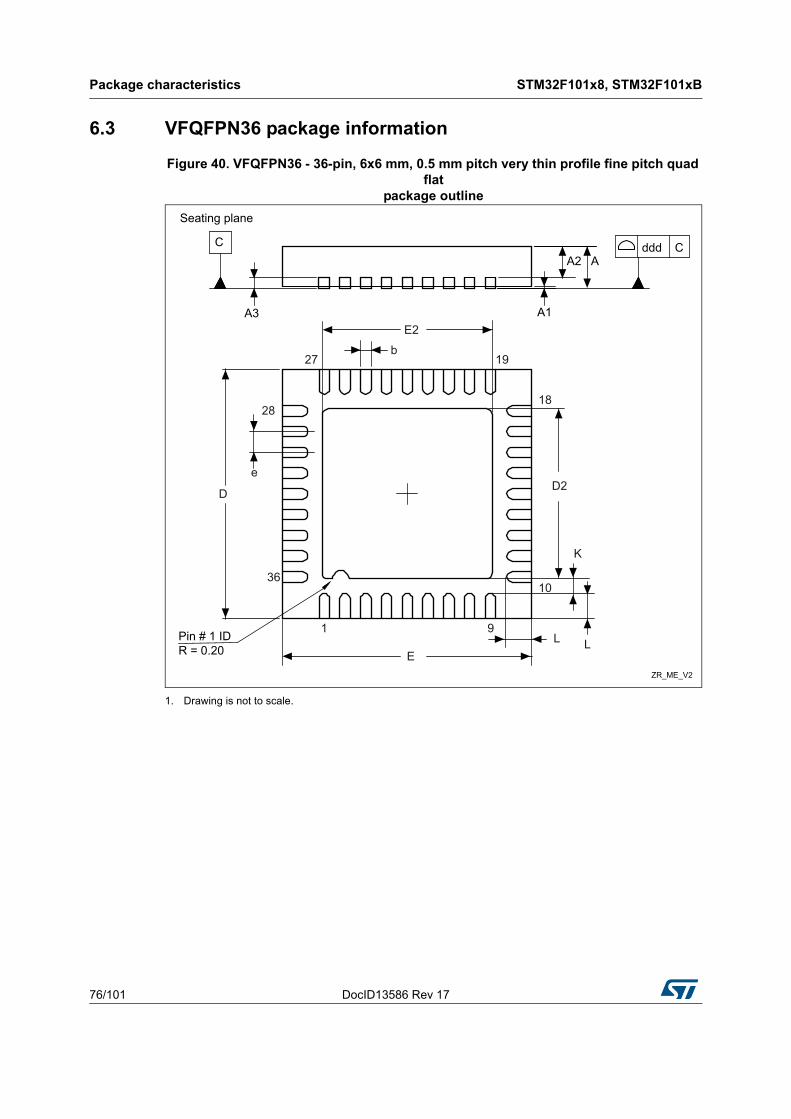
Package characteristics STM32F101x8, STM32F101xB
76/101 DocID13586 Rev 17
6.3 VFQFPN36 package information
Figure 40. VFQFPN36 - 36-pin, 6x6 mm, 0.5 mm pitch very thin profile fine pitch quad flat
package outline
1. Drawing is not to scale.
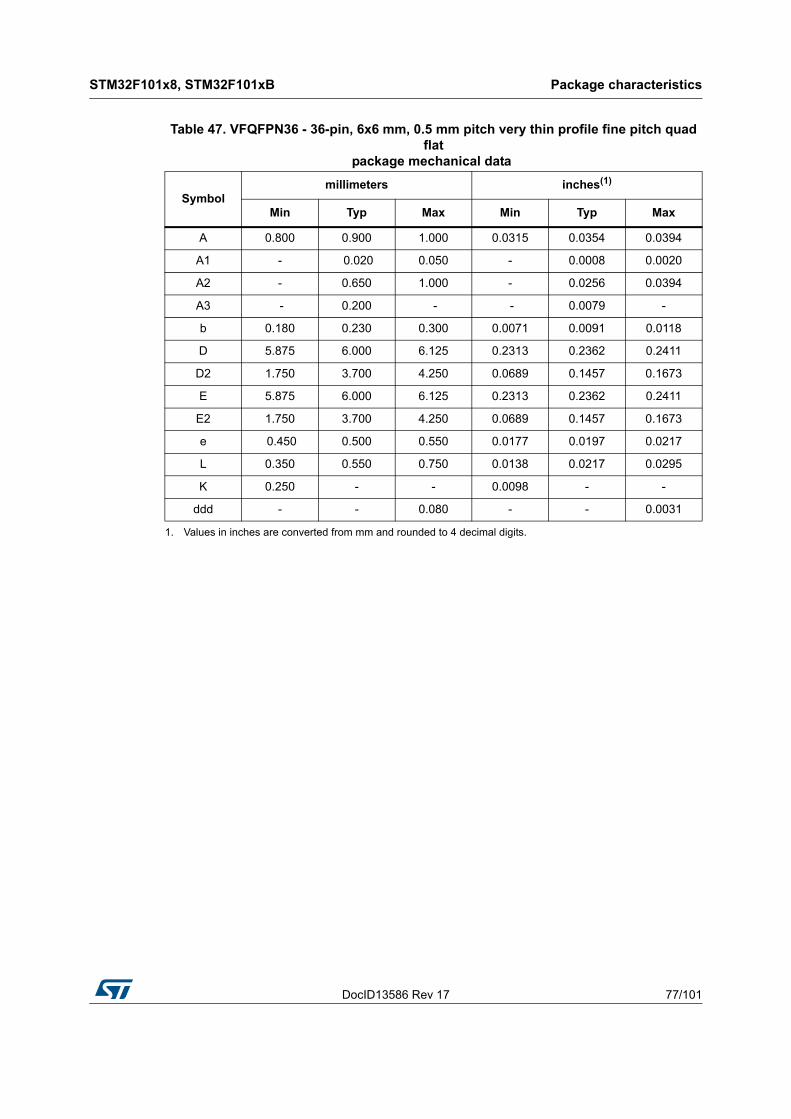
DocID13586 Rev 17 77/101
STM32F101x8, STM32F101xB Package characteristics
100
Table 47. VFQFPN36 - 36-pin, 6x6 mm, 0.5 mm pitch very thin profile fine pitch quad flat
package mechanical data
Symbolmillimeters inches(1)
1. Values in inches are converted from mm and rounded to 4 decimal digits.
Min Typ Max Min Typ Max
A 0.800 0.900 1.000 0.0315 0.0354 0.0394
A1 - 0.020 0.050 - 0.0008 0.0020
A2 - 0.650 1.000 - 0.0256 0.0394
A3 - 0.200 - - 0.0079 -
b 0.180 0.230 0.300 0.0071 0.0091 0.0118
D 5.875 6.000 6.125 0.2313 0.2362 0.2411
D2 1.750 3.700 4.250 0.0689 0.1457 0.1673
E 5.875 6.000 6.125 0.2313 0.2362 0.2411
E2 1.750 3.700 4.250 0.0689 0.1457 0.1673
e 0.450 0.500 0.550 0.0177 0.0197 0.0217
L 0.350 0.550 0.750 0.0138 0.0217 0.0295
K 0.250 - - 0.0098 - -
ddd - - 0.080 - - 0.0031
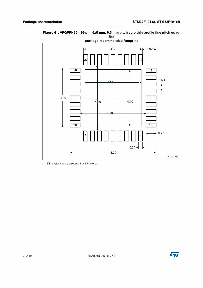
Package characteristics STM32F101x8, STM32F101xB
78/101 DocID13586 Rev 17
Figure 41. VFQFPN36 - 36-pin, 6x6 mm, 0.5 mm pitch very thin profile fine pitch quad flat
package recommended footprint
1. Dimensions are expressed in millimeters.
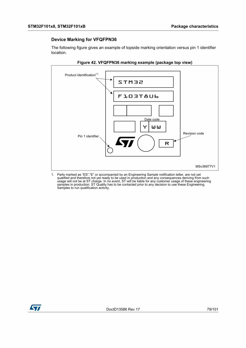
DocID13586 Rev 17 79/101
STM32F101x8, STM32F101xB Package characteristics
100
Device Marking for VFQFPN36
The following figure gives an example of topside marking orientation versus pin 1 identifier location.
Figure 42. VFQFPN36 marking example (package top view)
1. Parts marked as “ES”,”E” or accompanied by an Engineering Sample notification letter, are not yet qualified and therefore not yet ready to be used in production and any consequences deriving from such usage will not be at ST charge. In no event, ST will be liable for any customer usage of these engineering samples in production. ST Quality has to be contacted prior to any decision to use these Engineering Samples to run qualification activity.
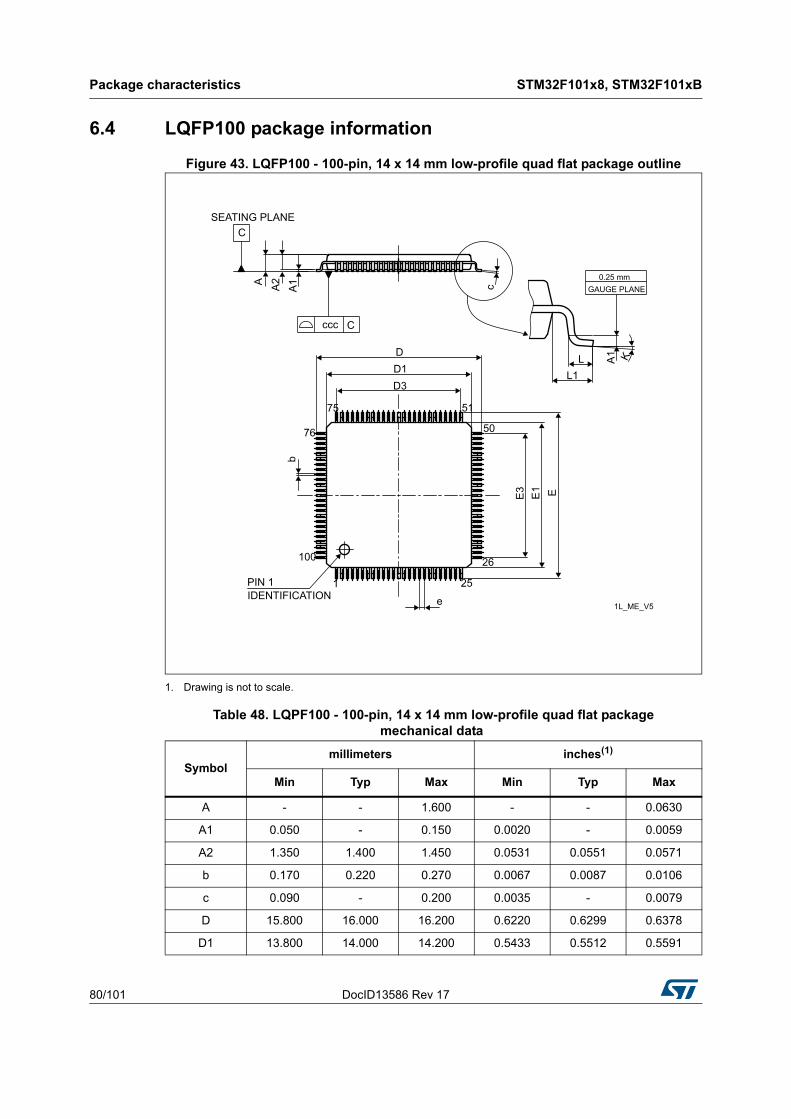
Package characteristics STM32F101x8, STM32F101xB
80/101 DocID13586 Rev 17
6.4 LQFP100 package information
Figure 43. LQFP100 - 100-pin, 14 x 14 mm low-profile quad flat package outline
1. Drawing is not to scale.
Table 48. LQPF100 - 100-pin, 14 x 14 mm low-profile quad flat package mechanical data
Symbolmillimeters inches(1)
Min Typ Max Min Typ Max
A - - 1.600 - - 0.0630
A1 0.050 - 0.150 0.0020 - 0.0059
A2 1.350 1.400 1.450 0.0531 0.0551 0.0571
b 0.170 0.220 0.270 0.0067 0.0087 0.0106
c 0.090 - 0.200 0.0035 - 0.0079
D 15.800 16.000 16.200 0.6220 0.6299 0.6378
D1 13.800 14.000 14.200 0.5433 0.5512 0.5591
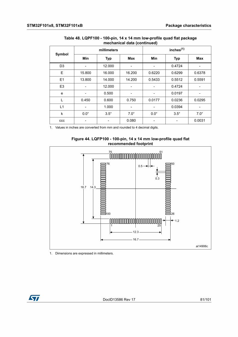
DocID13586 Rev 17 81/101
STM32F101x8, STM32F101xB Package characteristics
100
Figure 44. LQFP100 - 100-pin, 14 x 14 mm low-profile quad flat recommended footprint
1. Dimensions are expressed in millimeters.
D3 - 12.000 - - 0.4724 -
E 15.800 16.000 16.200 0.6220 0.6299 0.6378
E1 13.800 14.000 14.200 0.5433 0.5512 0.5591
E3 - 12.000 - - 0.4724 -
e - 0.500 - - 0.0197 -
L 0.450 0.600 0.750 0.0177 0.0236 0.0295
L1 - 1.000 - - 0.0394 -
k 0.0° 3.5° 7.0° 0.0° 3.5° 7.0°
ccc - - 0.080 - - 0.0031
1. Values in inches are converted from mm and rounded to 4 decimal digits.
Table 48. LQPF100 - 100-pin, 14 x 14 mm low-profile quad flat package mechanical data (continued)
Symbolmillimeters inches(1)
Min Typ Max Min Typ Max
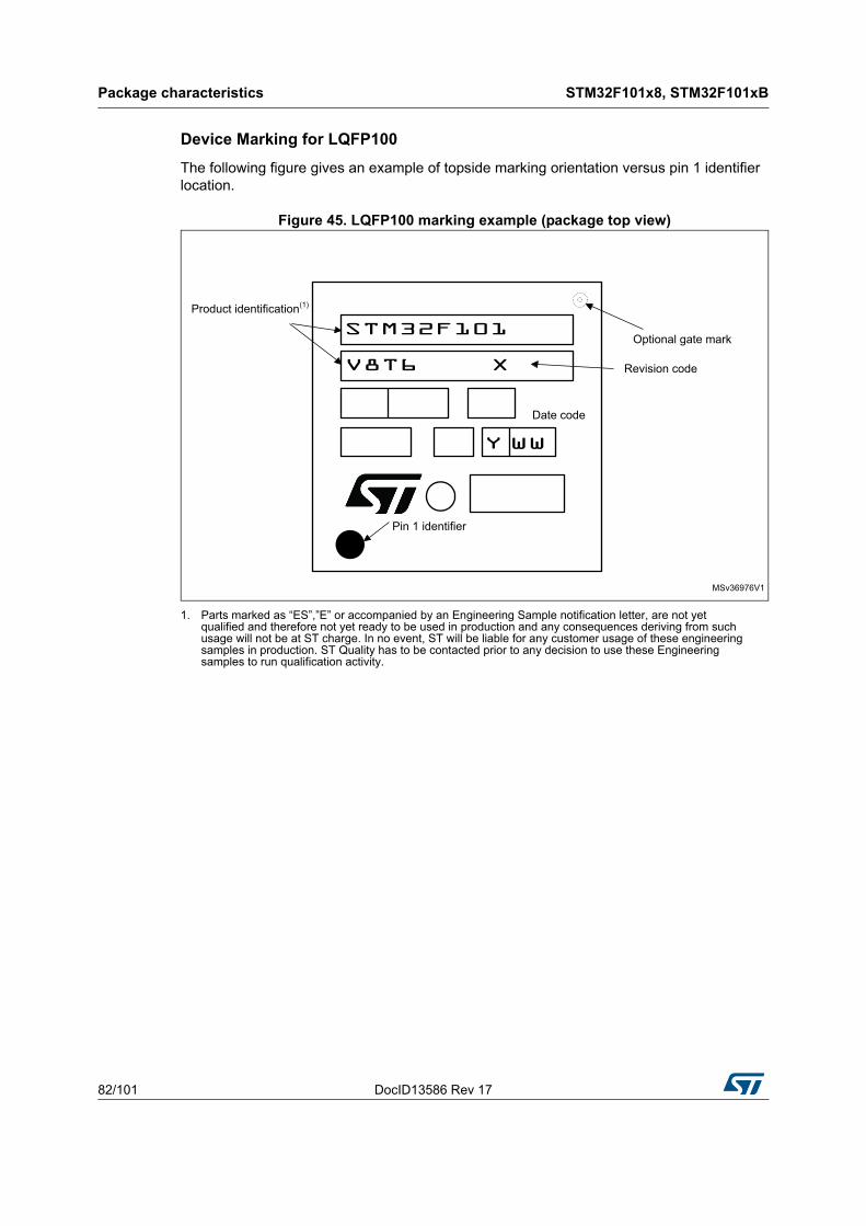
Package characteristics STM32F101x8, STM32F101xB
82/101 DocID13586 Rev 17
Device Marking for LQFP100
The following figure gives an example of topside marking orientation versus pin 1 identifier location.
Figure 45. LQFP100 marking example (package top view)
1. Parts marked as “ES”,”E” or accompanied by an Engineering Sample notification letter, are not yet qualified and therefore not yet ready to be used in production and any consequences deriving from such usage will not be at ST charge. In no event, ST will be liable for any customer usage of these engineering samples in production. ST Quality has to be contacted prior to any decision to use these Engineering samples to run qualification activity.
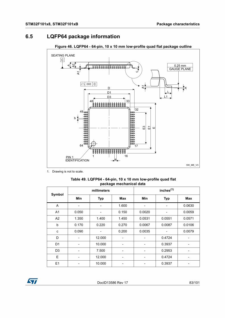
DocID13586 Rev 17 83/101
STM32F101x8, STM32F101xB Package characteristics
100
6.5 LQFP64 package information
Figure 46. LQFP64 - 64-pin, 10 x 10 mm low-profile quad flat package outline
1. Drawing is not to scale.
Table 49. LQFP64 - 64-pin, 10 x 10 mm low-profile quad flat package mechanical data
Symbolmillimeters inches(1)
Min Typ Max Min Typ Max
A - - 1.600 - - 0.0630
A1 0.050 - 0.150 0.0020 - 0.0059
A2 1.350 1.400 1.450 0.0531 0.0551 0.0571
b 0.170 0.220 0.270 0.0067 0.0087 0.0106
c 0.090 - 0.200 0.0035 - 0.0079
D - 12.000 - - 0.4724 -
D1 - 10.000 - - 0.3937 -
D3 - 7.500 - - 0.2953 -
E - 12.000 - - 0.4724 -
E1 - 10.000 - - 0.3937 -
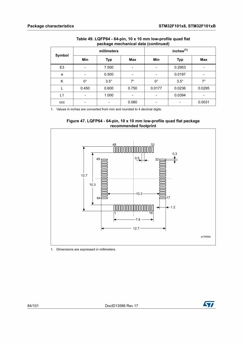
Package characteristics STM32F101x8, STM32F101xB
84/101 DocID13586 Rev 17
Figure 47. LQFP64 - 64-pin, 10 x 10 mm low-profile quad flat package recommended footprint
1. Dimensions are expressed in millimeters.
E3 - 7.500 - - 0.2953 -
e - 0.500 - - 0.0197 -
K 0° 3.5° 7° 0° 3.5° 7°
L 0.450 0.600 0.750 0.0177 0.0236 0.0295
L1 - 1.000 - - 0.0394 -
ccc - - 0.080 - - 0.0031
1. Values in inches are converted from mm and rounded to 4 decimal digits.
Table 49. LQFP64 - 64-pin, 10 x 10 mm low-profile quad flat package mechanical data (continued)
Symbolmillimeters inches(1)
Min Typ Max Min Typ Max
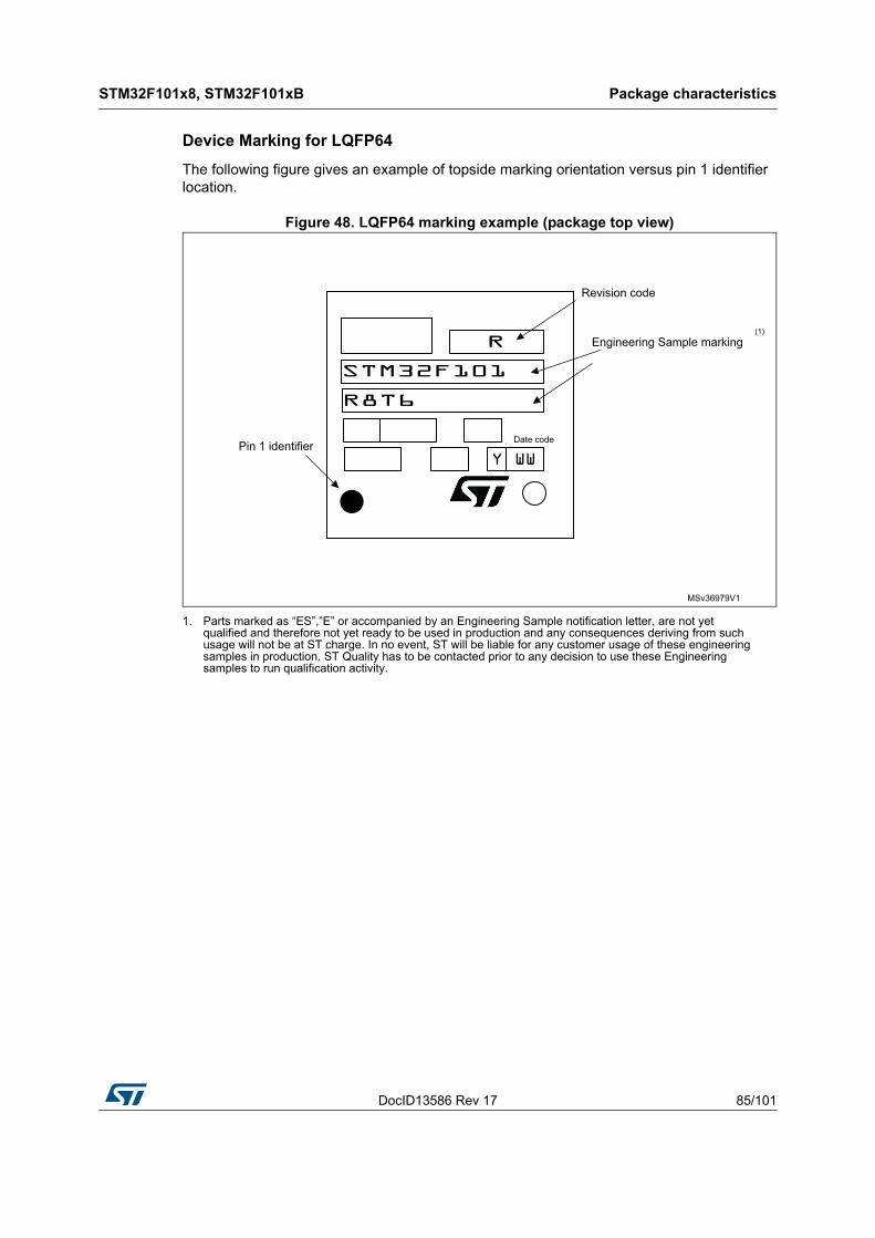
DocID13586 Rev 17 85/101
STM32F101x8, STM32F101xB Package characteristics
100
Device Marking for LQFP64
The following figure gives an example of topside marking orientation versus pin 1 identifier location.
Figure 48. LQFP64 marking example (package top view)
1. Parts marked as “ES”,”E” or accompanied by an Engineering Sample notification letter, are not yet qualified and therefore not yet ready to be used in production and any consequences deriving from such usage will not be at ST charge. In no event, ST will be liable for any customer usage of these engineering samples in production. ST Quality has to be contacted prior to any decision to use these Engineering samples to run qualification activity.
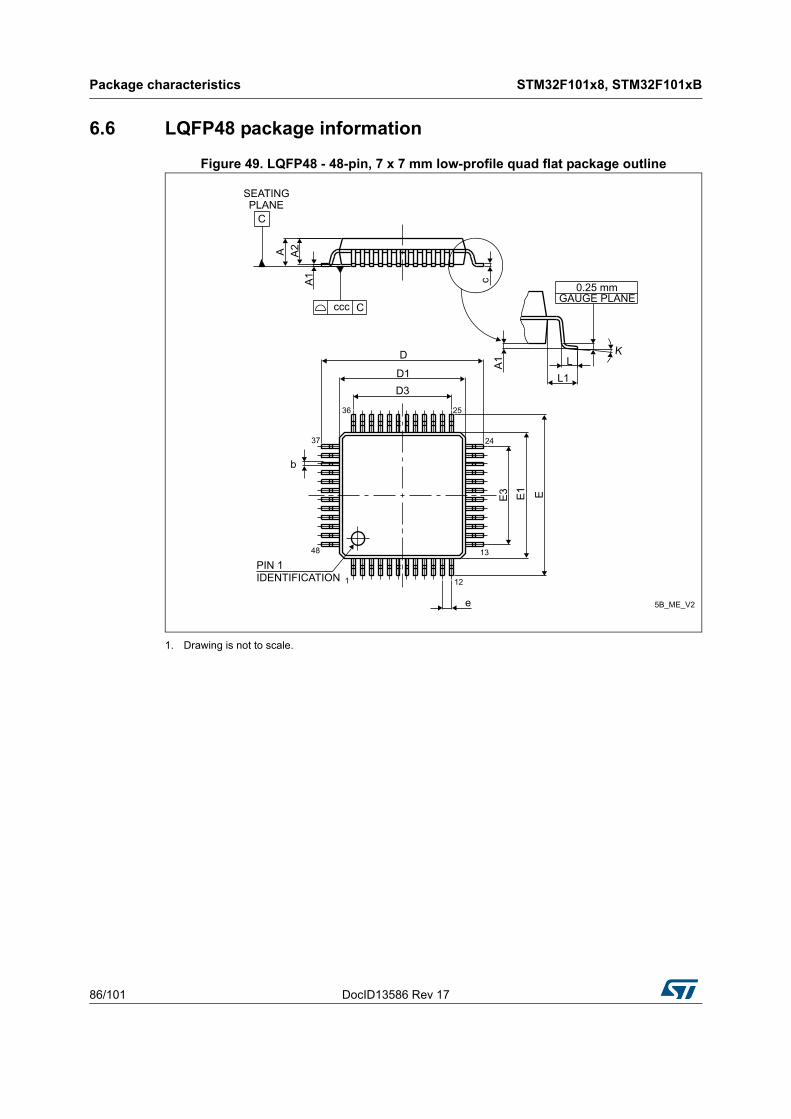
Package characteristics STM32F101x8, STM32F101xB
86/101 DocID13586 Rev 17
6.6 LQFP48 package information
Figure 49. LQFP48 - 48-pin, 7 x 7 mm low-profile quad flat package outline
1. Drawing is not to scale.
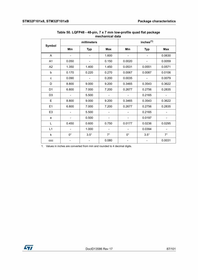
DocID13586 Rev 17 87/101
STM32F101x8, STM32F101xB Package characteristics
100
Table 50. LQFP48 - 48-pin, 7 x 7 mm low-profile quad flat package mechanical data
Symbolmillimeters inches(1)
1. Values in inches are converted from mm and rounded to 4 decimal digits.
Min Typ Max Min Typ Max
A - - 1.600 - - 0.0630
A1 0.050 - 0.150 0.0020 - 0.0059
A2 1.350 1.400 1.450 0.0531 0.0551 0.0571
b 0.170 0.220 0.270 0.0067 0.0087 0.0106
c 0.090 - 0.200 0.0035 - 0.0079
D 8.800 9.000 9.200 0.3465 0.3543 0.3622
D1 6.800 7.000 7.200 0.2677 0.2756 0.2835
D3 - 5.500 - - 0.2165 -
E 8.800 9.000 9.200 0.3465 0.3543 0.3622
E1 6.800 7.000 7.200 0.2677 0.2756 0.2835
E3 - 5.500 - - 0.2165 -
e - 0.500 - - 0.0197 -
L 0.450 0.600 0.750 0.0177 0.0236 0.0295
L1 - 1.000 - - 0.0394 -
k 0° 3.5° 7° 0° 3.5° 7°
ccc - - 0.080 - - 0.0031
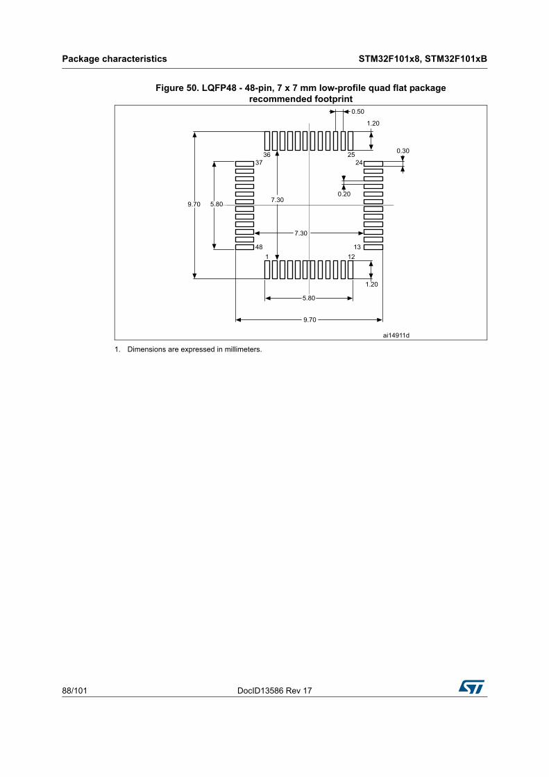
Package characteristics STM32F101x8, STM32F101xB
88/101 DocID13586 Rev 17
Figure 50. LQFP48 - 48-pin, 7 x 7 mm low-profile quad flat package recommended footprint
1. Dimensions are expressed in millimeters.

DocID13586 Rev 17 89/101
STM32F101x8, STM32F101xB Package characteristics
100
Device Marking for LQFP48
The following figure gives an example of topside marking orientation versus pin 1 identifier location.
Figure 51. LQFP48 marking example (package top view)
1. Parts marked as “ES”,”E” or accompanied by an Engineering Sample notification letter, are not yet qualified and therefore not yet ready to be used in production and any consequences deriving from such usage will not be at ST charge. In no event, ST will be liable for any customer usage of these engineering samples in production. ST Quality has to be contacted prior to any decision to use these Engineering samples to run qualification activity.
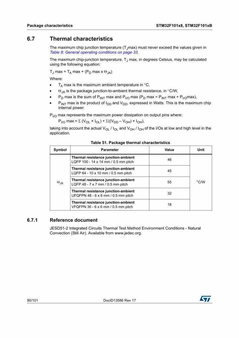
Package characteristics STM32F101x8, STM32F101xB
90/101 DocID13586 Rev 17
6.7 Thermal characteristics
The maximum chip junction temperature (TJmax) must never exceed the values given in Table 8: General operating conditions on page 33.
The maximum chip-junction temperature, TJ max, in degrees Celsius, may be calculated using the following equation:
TJ max = TA max + (PD max x JA)
Where:
TA max is the maximum ambient temperature in C,
JA is the package junction-to-ambient thermal resistance, in C/W,
PD max is the sum of PINT max and PI/O max (PD max = PINT max + PI/Omax),
PINT max is the product of IDD and VDD, expressed in Watts. This is the maximum chip internal power.
PI/O max represents the maximum power dissipation on output pins where:
PI/O max = (VOL × IOL) + ((VDD – VOH) × IOH),
taking into account the actual VOL / IOL and VOH / IOH of the I/Os at low and high level in the application.
6.7.1 Reference document
JESD51-2 Integrated Circuits Thermal Test Method Environment Conditions - Natural Convection (Still Air). Available from www.jedec.org.
Table 51. Package thermal characteristics
Symbol Parameter Value Unit
JA
Thermal resistance junction-ambientLQFP 100 - 14 x 14 mm / 0.5 mm pitch
46
°C/W
Thermal resistance junction-ambientLQFP 64 - 10 x 10 mm / 0.5 mm pitch
45
Thermal resistance junction-ambientLQFP 48 - 7 x 7 mm / 0.5 mm pitch
55
Thermal resistance junction-ambientUFQFPN 48 - 6 x 6 mm / 0.5 mm pitch
32
Thermal resistance junction-ambientVFQFPN 36 - 6 x 6 mm / 0.5 mm pitch
18
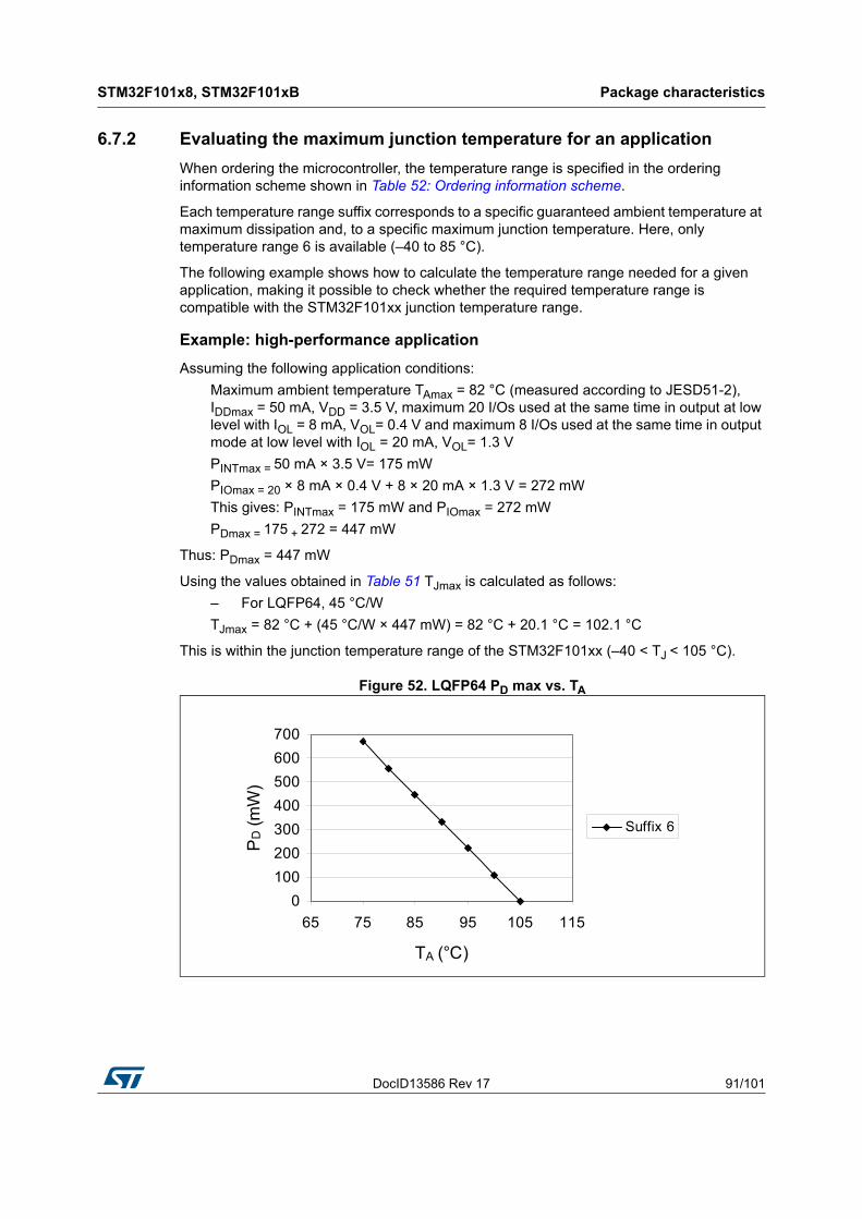
DocID13586 Rev 17 91/101
STM32F101x8, STM32F101xB Package characteristics
100
6.7.2 Evaluating the maximum junction temperature for an application
When ordering the microcontroller, the temperature range is specified in the ordering information scheme shown in Table 52: Ordering information scheme.
Each temperature range suffix corresponds to a specific guaranteed ambient temperature at maximum dissipation and, to a specific maximum junction temperature. Here, only temperature range 6 is available (–40 to 85 °C).
The following example shows how to calculate the temperature range needed for a given application, making it possible to check whether the required temperature range is compatible with the STM32F101xx junction temperature range.
Example: high-performance application
Assuming the following application conditions:
Maximum ambient temperature TAmax = 82 °C (measured according to JESD51-2), IDDmax = 50 mA, VDD = 3.5 V, maximum 20 I/Os used at the same time in output at low level with IOL = 8 mA, VOL= 0.4 V and maximum 8 I/Os used at the same time in output mode at low level with IOL = 20 mA, VOL= 1.3 V
PINTmax = 50 mA × 3.5 V= 175 mW
PIOmax = 20 × 8 mA × 0.4 V + 8 × 20 mA × 1.3 V = 272 mW
This gives: PINTmax = 175 mW and PIOmax = 272 mW
PDmax = 175 + 272 = 447 mW
Thus: PDmax = 447 mW
Using the values obtained in Table 51 TJmax is calculated as follows:
– For LQFP64, 45 °C/W
TJmax = 82 °C + (45 °C/W × 447 mW) = 82 °C + 20.1 °C = 102.1 °C
This is within the junction temperature range of the STM32F101xx (–40 < TJ < 105 °C).
Figure 52. LQFP64 PD max vs. TA
0
100
200
300
400
500
600
700
65 75 85 95 105 115
TA (°C)
PD (
mW
)
Suffix 6
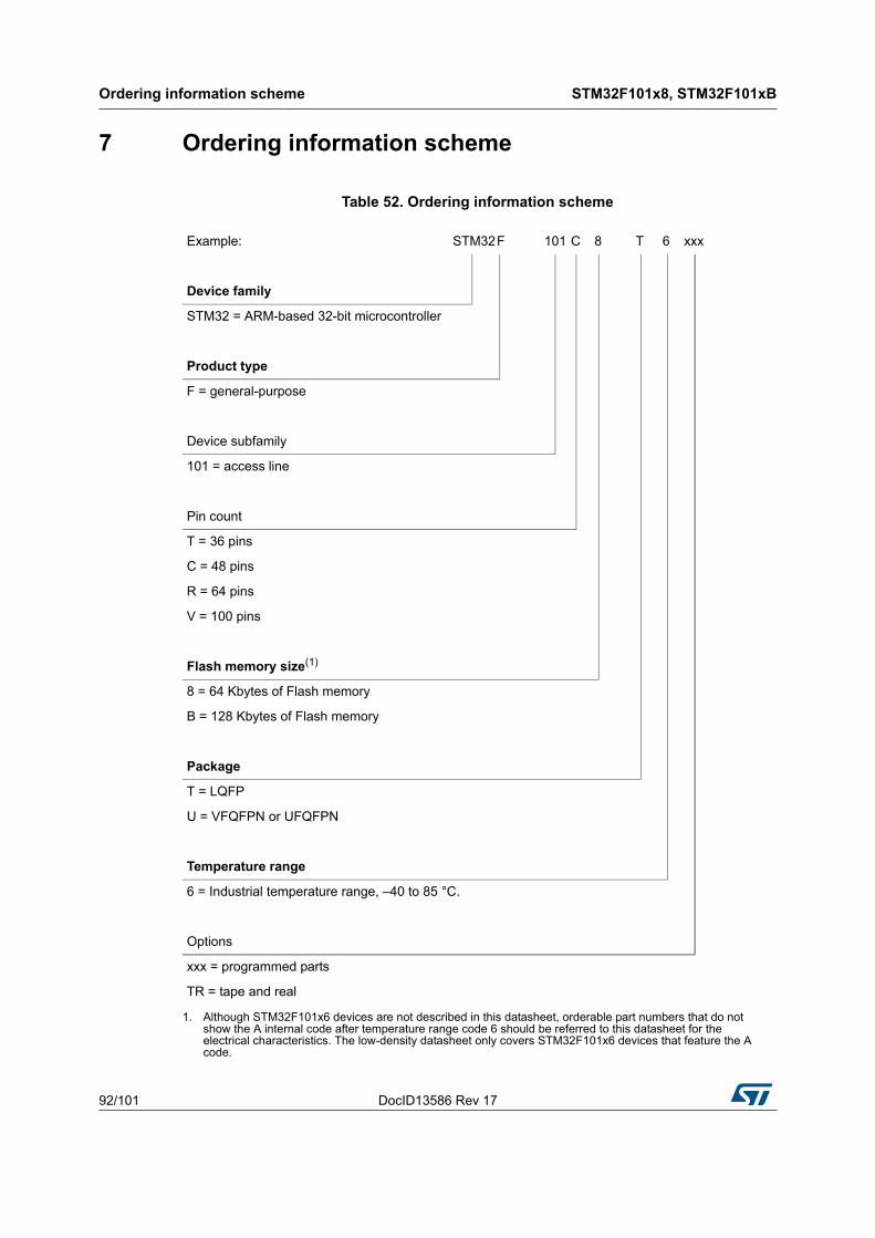
Ordering information scheme STM32F101x8, STM32F101xB
92/101 DocID13586 Rev 17
7 Ordering information scheme
Table 52. Ordering information scheme
Example: STM32F 101 C 8 T 6 xxx
Device family
STM32 = ARM-based 32-bit microcontroller
Product type
F = general-purpose
Device subfamily
101 = access line
Pin count
T = 36 pins
C = 48 pins
R = 64 pins
V = 100 pins
Flash memory size(1)
1. Although STM32F101x6 devices are not described in this datasheet, orderable part numbers that do not show the A internal code after temperature range code 6 should be referred to this datasheet for the electrical characteristics. The low-density datasheet only covers STM32F101x6 devices that feature the A code.
8 = 64 Kbytes of Flash memory
B = 128 Kbytes of Flash memory
Package
T = LQFP
U = VFQFPN or UFQFPN
Temperature range
6 = Industrial temperature range, –40 to 85 °C.
Options
xxx = programmed parts
TR = tape and real
DocID13586 Rev 17 93/101
STM32F101x8, STM32F101xB Ordering information scheme
100
For a list of available options (speed, package, etc.) or for further information on any aspect of this device, please contact the nearest ST sales office.
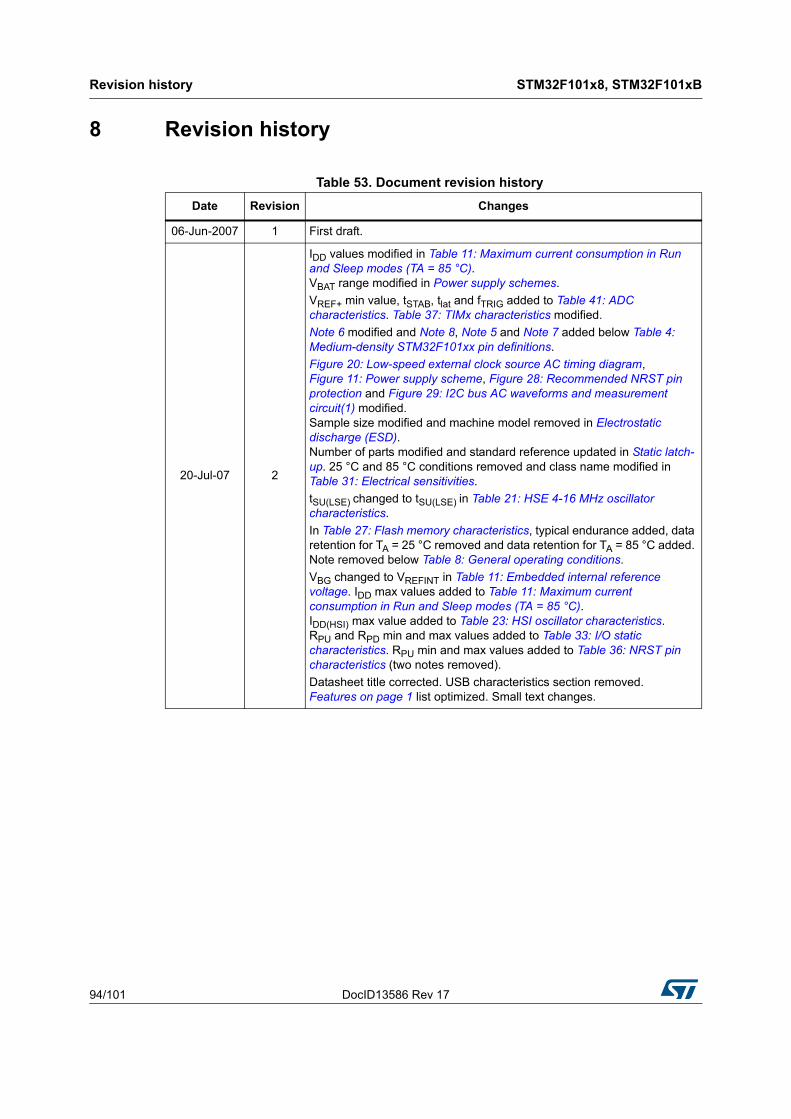
Revision history STM32F101x8, STM32F101xB
94/101 DocID13586 Rev 17
8 Revision history
Table 53. Document revision history
Date Revision Changes
06-Jun-2007 1 First draft.
20-Jul-07 2
IDD values modified in Table 11: Maximum current consumption in Run and Sleep modes (TA = 85 °C).VBAT range modified in Power supply schemes.
VREF+ min value, tSTAB, tlat and fTRIG added to Table 41: ADC characteristics. Table 37: TIMx characteristics modified.
Note 6 modified and Note 8, Note 5 and Note 7 added below Table 4: Medium-density STM32F101xx pin definitions.
Figure 20: Low-speed external clock source AC timing diagram, Figure 11: Power supply scheme, Figure 28: Recommended NRST pin protection and Figure 29: I2C bus AC waveforms and measurement circuit(1) modified.Sample size modified and machine model removed in Electrostatic discharge (ESD).Number of parts modified and standard reference updated in Static latch-up. 25 °C and 85 °C conditions removed and class name modified in Table 31: Electrical sensitivities.
tSU(LSE) changed to tSU(LSE) in Table 21: HSE 4-16 MHz oscillator characteristics.
In Table 27: Flash memory characteristics, typical endurance added, data retention for TA = 25 °C removed and data retention for TA = 85 °C added. Note removed below Table 8: General operating conditions.
VBG changed to VREFINT in Table 11: Embedded internal reference voltage. IDD max values added to Table 11: Maximum current consumption in Run and Sleep modes (TA = 85 °C).IDD(HSI) max value added to Table 23: HSI oscillator characteristics.RPU and RPD min and max values added to Table 33: I/O static characteristics. RPU min and max values added to Table 36: NRST pin characteristics (two notes removed).
Datasheet title corrected. USB characteristics section removed.Features on page 1 list optimized. Small text changes.
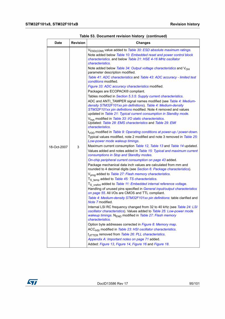
DocID13586 Rev 17 95/101
STM32F101x8, STM32F101xB Revision history
100
18-Oct-2007 3
VESD(CDM) value added to Table 30: ESD absolute maximum ratings.
Note added below Table 10: Embedded reset and power control block characteristics. and below Table 21: HSE 4-16 MHz oscillator characteristics.
Note added below Table 34: Output voltage characteristics and VOH parameter description modified.
Table 41: ADC characteristics and Table 43: ADC accuracy - limited test conditions modified.
Figure 33: ADC accuracy characteristics modified.
Packages are ECOPACK® compliant.
Tables modified in Section 5.3.5: Supply current characteristics.
ADC and ANTI_TAMPER signal names modified (see Table 4: Medium-density STM32F101xx pin definitions). Table 4: Medium-density STM32F101xx pin definitions modified. Note 4 removed and values updated in Table 21: Typical current consumption in Standby mode.
Vhys modified in Table 33: I/O static characteristics.Updated: Table 28: EMS characteristics and Table 29: EMI characteristics.
tVDD modified in Table 9: Operating conditions at power-up / power-down.
Typical values modified, note 2 modified and note 3 removed in Table 25: Low-power mode wakeup timings.
Maximum current consumption Table 12, Table 13 and Table 14 updated.
Values added and notes added in Table 15: Typical and maximum current consumptions in Stop and Standby modes.
On-chip peripheral current consumption on page 43 added.
Package mechanical data inch values are calculated from mm and rounded to 4 decimal digits (see Section 6: Package characteristics).
Vprog added to Table 27: Flash memory characteristics.
TS_temp added to Table 45: TS characteristics.
TS_vrefint added to Table 11: Embedded internal reference voltage.
Handling of unused pins specified in General input/output characteristics on page 55. All I/Os are CMOS and TTL compliant.
Table 4: Medium-density STM32F101xx pin definitions: table clarified and Note 7 modified.
Internal LSI RC frequency changed from 32 to 40 kHz (see Table 24: LSI oscillator characteristics). Values added to Table 25: Low-power mode wakeup timings. NEND modified in Table 27: Flash memory characteristics.
Option byte addresses corrected in Figure 8: Memory map.
ACCHSI modified in Table 23: HSI oscillator characteristics.
tJITTER removed from Table 26: PLL characteristics.
Appendix A: Important notes on page 71 added.
Added: Figure 13, Figure 14, Figure 16 and Figure 18.
Table 53. Document revision history (continued)
Date Revision Changes
Revision history STM32F101x8, STM32F101xB
96/101 DocID13586 Rev 17
22-Nov-2007 4
Document status promoted from preliminary data to datasheet. Small text changes.
STM32F101CB part number corrected in Table 1: Device summary.
Number of communication peripherals corrected for STM32F101Tx in Table 2: Device features and peripheral counts (STM32F101xx medium-density access line) and Number of GPIOs corrected for LQFP package.
Power supply schemes on page 16 modified.
Main function and default alternate function modified for PC14 and PC15 in Table 4: Medium-density STM32F101xx pin definitions, Note 6 added, Remap column added.
Figure 11: Power supply scheme modified. VDD VSS ratings modified and Note 1 modified in Table 5: Voltage characteristics. Note 1 modified in Table 6: Current characteristics.
Note 2 added in Table 10: Embedded reset and power control block characteristics.
48 and 72 MHz frequencies removed from Table 12, Table 13 and Table 14. MCU ‘s operating conditions modified in Typical current consumption on page 42. IDD_VBAT typical value at 2.4 V modified and IDD_VBAT maximum value added in Table 15: Typical and maximum current consumptions in Stop and Standby modes. Note added in Table 16 on page 42 and Table 17 on page 43. Table 18: Peripheral current consumption modified.
Figure 17: Typical current consumption in Stop mode with regulator in Low-power mode versus temperature at VDD = 3.3 V and 3.6 V added.
Note removed below Figure 30: SPI timing diagram - slave mode and CPHA = 0. Note added below Figure 31: SPI timing diagram - slave mode and CPHA = 1(1).
Figure 34: Typical connection diagram using the ADC modified.tSU(HSE) and tSU(LSE) conditions modified in Table 21 and Table 22, respectively. Maximum values removed from Table 25: Low-power mode wakeup timings. tRET conditions modified in Table 27: Flash memory characteristics. Conditions modified in Table 28: EMS characteristics.
Impedance size specified in A.4: Voltage glitch on ADC input 0 on page 71. Small text changes in Table 34: Output voltage characteristics.
Section 5.3.11: Absolute maximum ratings (electrical sensitivity) updated.
Details on unused pins removed from General input/output characteristics on page 55.
Table 40: SPI characteristics updated. Notes added and Ilkg removed in Table 41: ADC characteristics. Note added in Table 42 and Table 45. Note 3 and Note 2 added below Table 43: ADC accuracy - limited test conditions. Avg_Slope and V25 modified in Table 45: TS characteristics.JAvalue for VFQFPN36 package added in Table 51: Package thermal characteristicsI2C interface characteristics on page 62 modified.
Order codes replaced by Section 7: Ordering information scheme.
Table 53. Document revision history (continued)
Date Revision Changes
DocID13586 Rev 17 97/101
STM32F101x8, STM32F101xB Revision history
100
14-Mar-2008 5
Figure 2: Clock tree on page 13 added.
CRC added (see CRC (cyclic redundancy check) calculation unit on page 9 and Figure 8: Memory map on page 29 for address).
Maximum TJ value given in Table 7: Thermal characteristics on page 33.
PD, TA and TJ added, tprog values modified and tprog description clarified in Table 27: Flash memory characteristics on page 51.
IDD modified in Table 15: Typical and maximum current consumptions in Stop and Standby modes on page 39.
ACCHSI modified in Table 23: HSI oscillator characteristics on page 49, note 2 removed.
tRET modified in Table 27: Flash memory characteristics.
VNF(NRST) unit corrected in Table 36: NRST pin characteristics on page 60.
Table 40: SPI characteristics on page 65 modified.
IVREF added in Table 41: ADC characteristics on page 68.
Table 43: ADC accuracy - limited test conditions added. Table 44: ADC accuracy modified.
LQFP100 package specifications updated (see Section 6: Package characteristics on page 73).
Recommended LQFP100, LQFP64, LQFP48 and VFQFPN36 footprints added (see Figure 44, Figure 47, Figure 50 and Figure 41).
Section 6.7: Thermal characteristics on page 90 modified.
Appendix A: Important notes removed.
21-Mar-2008 6
Small text changes.
In Table 27: Flash memory characteristics:
– NEND tested over the whole temperature range
– cycling conditions specified for tRET
– tRET min modified at TA = 55 °C
Figure 2: Clock tree corrected. Figure 8: Memory map clarified.
V25, Avg_Slope and TL modified in Table 45: TS characteristics.
CRC feature removed.
22-May-2008 7
Section 1: Introduction modified, Section 2.2: Full compatibility throughout the family added. CRC feature added.
IDD_VBAT removed from Table 21: Typical current consumption in Standby mode on page 42.Values added to Table 39: SCL frequency (fPCLK1= 36 MHz, VDD_I2C = 3.3 V) on page 64.
Figure 30: SPI timing diagram - slave mode and CPHA = 0 on page 66 modified. Equation 1 corrected.
Section 6.7.2: Evaluating the maximum junction temperature for an application on page 91 added.
Axx option added to Table 52: Ordering information scheme on page 92.
Table 53. Document revision history (continued)
Date Revision Changes
Revision history STM32F101x8, STM32F101xB
98/101 DocID13586 Rev 17
21-Jul-2008 8
Small text changes.
Power supply supervisor on page 16 modified and VDDA added to Table 8: General operating conditions on page 33.
Capacitance modified in Figure 11: Power supply scheme on page 31.
Table notes revised in Section 5: Electrical characteristics.
Maximum value of tRSTTEMPO modified in Table 10: Embedded reset and power control block characteristics on page 35.
Values added to Table 15: Typical and maximum current consumptions in Stop and Standby modes and Table 21: Typical current consumption in Standby mode removed.
fHSE_ext modified in Table 19: High-speed external user clock characteristics on page 45. fPLL_IN modified in Table 26: PLL characteristics on page 50.
fHCLK corrected in Table 28: EMS characteristics.
Minimum SDA and SCL fall time value for Fast mode removed from Table 38: I2C characteristics on page 63, note 1 modified.
th(NSS) modified in Table 40: SPI characteristics on page 65 and Figure 30: SPI timing diagram - slave mode and CPHA = 0 on page 66.
CADC modified in Table 41: ADC characteristics on page 68 and Figure 34: Typical connection diagram using the ADC modified.
fPCLK2 corrected in Table 43: ADC accuracy - limited test conditions and Table 44: ADC accuracy.
Typical TS_temp value removed from Table 45: TS characteristics on page 72.
LQFP48 package specifications updated (see Table 50, Table 49 and Table 50).
Axx option removed from Table 52: Ordering information scheme on page 92.
24-Jul-2008 9 First page modified: “Up to 2 x I²C interfaces” instead of “1 x I²C interface”
23-Sep-2008 10
STM32F101xx devices with 32 Kbyte Flash memory capacity removed, document updated accordingly.
Section 2.2: Full compatibility throughout the family on page 14 updated.
Notes modified in Table 4: Medium-density STM32F101xx pin definitions on page 24.
Note 2 modified below Table 5: Voltage characteristics on page 32, |VDDx| min and |VDDx| min removed.
Note 2 added to Table 8: General operating conditions on page 33.
Measurement conditions specified in Section 5.3.5: Supply current characteristics on page 36.
IDD in standby mode at 85 °C modified in Table 15: Typical and maximum current consumptions in Stop and Standby modes on page 39.
General input/output characteristics on page 55 modified.
Note added below Table 52: Ordering information scheme.
Section 7.1: Future family enhancements removed. Small text changes.
Table 53. Document revision history (continued)
Date Revision Changes
DocID13586 Rev 17 99/101
STM32F101x8, STM32F101xB Revision history
100
21-Apr-2009 11
I/O information clarified on page 1. Figure 8: Memory map modified.
In Table 4: Medium-density STM32F101xx pin definitions: PB4, PB13, PB14, PB15, PB3/TRACESWO moved from Default column to Remap column.
Note modified in Table 12: Maximum current consumption in Run mode, code with data processing running from Flash and Table 14: Maximum current consumption in Sleep mode, code running from Flash or RAM.
Figure 16, Figure 17 and Figure 18 show typical curves.Table 19: High-speed external user clock characteristics and Table 20: Low-speed external user clock characteristics modified.
ACCHSI max values modified in Table 23: HSI oscillator characteristics. Small text changes.
22-Sep-2009 12
Note 5 updated and Note 4 added in Table 4: Medium-density STM32F101xx pin definitions.
VRERINT and TCoeff added to Table 11: Embedded internal reference voltage. Typical IDD_VBAT value added in Table 15: Typical and maximum current consumptions in Stop and Standby modes. Figure 15: Typical current consumption on VBAT with RTC on versus temperature at different VBAT values added.
fHSE_ext min modified in Table 19: High-speed external user clock characteristics.
CL1 and CL2 replaced by C in Table 21: HSE 4-16 MHz oscillator characteristics and Table 22: LSE oscillator characteristics (fLSE = 32.768 kHz), notes modified and moved below the tables.
Table 23: HSI oscillator characteristics modified. Conditions removed from Table 25: Low-power mode wakeup timings.
Figure 28: Recommended NRST pin protection modified.
Note 1 modified below Figure 21: Typical application with an 8 MHz crystal.
Figure 28: Recommended NRST pin protection modified.
IEC 1000 standard updated to IEC 61000 and SAE J1752/3 updated to IEC 61967-2 in Section 5.3.10: EMC characteristics on page 51.
Jitter added to Table 26: PLL characteristics. CADC and RAIN parameters modified in Table 41: ADC characteristics. RAIN max values modified in Table 42: RAIN max for fADC = 14 MHz.
Small text changes.
20-May-2010 13
Added STM32F101TB devices.
Added VFQFPN48 package.
Updated note 2 below Table 38: I2C characteristics
Updated Figure 29: I2C bus AC waveforms and measurement circuit(1)
Updated Figure 28: Recommended NRST pin protection
Updated Section 5.3.12: I/O current injection characteristics
Table 53. Document revision history (continued)
Date Revision Changes
Revision history STM32F101x8, STM32F101xB
100/101 DocID13586 Rev 17
19-Apr-2011 14
Updated footnotes below Table 5: Voltage characteristics on page 32 and Table 6: Current characteristics on page 33
Updated tw min in Table 19: High-speed external user clock characteristics on page 45
Updated startup time in Table 22: LSE oscillator characteristics (fLSE = 32.768 kHz) on page 48
Added Section 5.3.12: I/O current injection characteristics
Updated Section 5.3.13: I/O port characteristics
15-May-2013 15
Replaced VQFN48 package with UQFN48 in cover page packages, Table 2: Device features and peripheral counts (STM32F101xx medium-density access line), Figure 7: STM32F101xx medium-density access line UVFQPFN48 pinout, Table 4: Medium-density STM32F101xx pin definitions, Figure 4: STM32F101xx medium-density access line LQFP64 pinout, added Figure 37: UFQFPN48 7 x 7 mm, 0.5 mm pitch, package outline, Table 47: UFQFPN48 7 x 7 mm, 0.5 mm pitch, package mechanical data, Table 52: Ordering information scheme and updated Table 51: Package thermal characteristics
Updated ‘All GPIOs are high current...’ in Section 2.3.22: GPIOs (general-purpose inputs/outputs)
Updated Table 4: Medium-density STM32F101xx pin definitions
Corrected Sigma letter in Section 5.1.1: Minimum and maximum values
Updated Table 6: Current characteristics
Added ‘VIN’ in Table 8: General operating conditions
Removed the first sentence in Section 5.3.16: Communications interfaces
Updated first sentence in Output driving current
Added note 5. in Table 23: HSI oscillator characteristics
Updated ‘VIL’ and ‘VIH’ in Table 33: I/O static characteristics
Added notes to Figure 23: Standard I/O input characteristics - CMOS port, Figure 24: Standard I/O input characteristics - TTL port, Figure 25: 5 V tolerant I/O input characteristics - CMOS port and Figure 26: 5 V tolerant I/O input characteristics - TTL port
Updated note 2. in Table 44: ADC accuracy
Updated Figure 29: I2C bus AC waveforms and measurement circuit(1)
Updated note 2. and 3.,removed note “the device must internally...” in Table 38: I2C characteristics
Updated title of Table 39: SCL frequency (fPCLK1= 36 MHz, VDD_I2C = 3.3 V)
05-Aug-2013 16
Updated the reference for ‘VESD(CDM)’ in Table 30: ESD absolute maximum ratings
Corrected ‘tf(IO)out’ in Figure 27: I/O AC characteristics definition
Updated Table 46: UFQFPN48 7 x 7 mm, 0.5 mm pitch, package mechanical data
19-Jun-2015 17Updated Section 6.1: Package mechanical data and Table 18: Peripheral current consumption.
Table 53. Document revision history (continued)
Date Revision Changes
DocID13586 Rev 17 101/101
STM32F101x8, STM32F101xB
101
IMPORTANT NOTICE – PLEASE READ CAREFULLY
STMicroelectronics NV and its subsidiaries (“ST”) reserve the right to make changes, corrections, enhancements, modifications, and improvements to ST products and/or to this document at any time without notice. Purchasers should obtain the latest relevant information on ST products before placing orders. ST products are sold pursuant to ST’s terms and conditions of sale in place at the time of order acknowledgement.
Purchasers are solely responsible for the choice, selection, and use of ST products and ST assumes no liability for application assistance or the design of Purchasers’ products.
No license, express or implied, to any intellectual property right is granted by ST herein.
Resale of ST products with provisions different from the information set forth herein shall void any warranty granted by ST for such product.
ST and the ST logo are trademarks of ST. All other product or service names are the property of their respective owners.
Information in this document supersedes and replaces information previously supplied in any prior versions of this document.
© 2015 STMicroelectronics – All rights reserved