Embed Size (px)
Citation preview
Mechanism of electromigration-induced failure in flip-chipsolder joints with a 10-µm-thick Cuunder-bump metallization
Jae-Woong Nah,a) Kai Chen, and K.N. TuDepartment of Materials Science and Engineering, University California at Los Angeles,Los Angeles, California 90095-1595
Bor-Rung Su and Chih ChenDepartment of Materials Science and Engineering, National Chiao Tung University,Taiwan 30050, People’s Republic of China
(Received 26 October 2006; accepted 7 December 2006)
The electromigration-induced failure in flip-chip eutectic SnPb solder joints with a10-�m-thick Cu under-bump metallization (UBM) was studied without the effect ofcurrent crowding in the solder region. The current crowding occurred inside the UBMinstead of in the solder joint at the current density of 3.0 × 10⁴ A/cm2 because of thespreading of current in the very thick Cu UBM. In these joints, the failure occurredthrough a two-stage consumption of the thick Cu UBM in the joint where electronsflowed from the chip to the substrate. In the first stage, the Cu UBM dissolved layerby layer rather uniformly across the entire Cu UBM–solder interface. In the secondstage, after half of the Cu UBM was dissolved, an asymmetrical dissolution ofCu UBM took place at the corner where electrons entered from the Al interconnect tothe Cu UBM. Experimental observation of dissolution steps of the 10-�m-thick CuUBM is presented. The transition from the first stage to the second stage has beenfound to depend on the location of current crowding in the flip-chip joints as theUBM thickness changes during the electromigration test. The current distributionin the flip-chip solder joints as a function of UBM thickness was simulated bythree-dimensional finite element analysis. The dissolution rate of Cu UBM in thesecond stage was faster than that in the first stage. The mechanism ofelectromigration-induced failure in the flip-chip solder joints with a 10-�m-thickCu UBM is discussed.
I. INTRODUCTION
Under-bump metallization (UBM) is very important inthe flip-chip technology because it acts as a solder wet-table layer, diffusion barrier, and adhesion layer.1 Cur-rently, the most common choices for solder wettable lay-ers are Cu and Au, and the diffusion barrier and adhesionlayers are TiW, Ti, Cr, Al, NiV, and Ni. These choicesdepend not only on a solder bumping process, but also ona balancing of capabilities and costs, as well as the manu-facturer’s skill and experience. When a trilayer thin filmof Cr/Cu/Au is applied as UBM, spalling of Cu–Sn com-pounds from the Cu–solder interface occurs and resultsin a weak mechanical solder joint, which is one of themost serious reliability problems because the Sn-based
Pb-free solders react very fast with Cu and the amount ofCu is very limited in the thin-film metallization.2–4 Toovercome the spalling problem, a 5-�m-thick electro-plated Cu UBM has been integrated into the UBM so thatthe chemical reaction will not consume all the Cu and nospalling may occur during aging.5 However, when thejoint is subjected to current stressing, current crowdingleads to a rapid dissolution of the 5-�m-thick Cu UBM atthe corner where electrons entered from Al interconnectto Cu UBM and the joint failed quickly.6 Due to thedemand for high performance and miniaturization in theelectronics industry, the problem of electromigrationmust be overcome; a thicker Cu UBM has been designedto overcome the electromigration-induced failure.7 Cur-rently, the design rule requires that each flip-chip solderjoint of 50 �m in diameter carries 0.2 A, which meansthat the average current density in such a joint is about104 A/cm2.7 The International Technology Roadmap forSemiconductor (ITRS) projections indicated that electro-migration is a near-term issue in high current densitypackages.8
a)Address all correspondence to this author.e-mail: [email protected] address: IBM T.J. Watson Research Center, YorktownHeights, NY.
DOI: 10.1557/JMR.2007.0084
J. Mater. Res., Vol. 22, No. 3, Mar 2007 © 2007 Materials Research Society 763
It is conceivable that if a thicker Cu UBM is used, alonger lifetime would be expected. However, the samefailure mechanism of the asymmetrical dissolution of CuUBM and short lifetime have been reported in the litera-ture even for solder joints with a 8.5-�m-thick Cu UBM.When the applied current was increased, the currentcrowding occurred at the UBM–solder interface and ledto fast failure.9–11 In this paper, the electromigration in a10-�m-thick Cu UBM under low current density hasbeen studied. While the current crowding area is locatedinitially inside the UBM, electromigration-induced fail-ure still occurs. We observed two-stage UBM consump-tion in this system during the electromigration test. At thefirst stage, the 10-�m-thick Cu UBM dissolved ratheruniformly at the entire Cu UBM–solder interface. In thesecond stage, when the Cu became thinner, the asym-metrical dissolution of Cu UBM due to the currentcrowding effect came back. A three-dimensional (3D)simulation was performed to show the distribution ofcurrent density during electromigration testing and tohelp understand the UBM–solder interfacial reactionwhen we attempt to avoid current crowding by using verythick Cu UBM.
II. EXPERIMENTAL
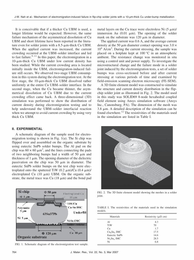
A schematic diagram of the sample used for electro-migration testing is shown in Fig. 1(a). The Si chip wasflipped over and assembled on the organic substrate byusing eutectic SnPb solder bumps. The Al pad on thechip was 60 × 60 �m2, and the lines connecting the padsof two neighboring bumps had a width of 50 �m andthickness of 1 �m. The opening diameter of the dielectricpassivation on the chip was 50 �m in diameter. Theeutectic SnPb solder bumps on the test chip were elec-troplated onto the sputtered TiW (0.2 �m)/Cu (0.4 �m)/electroplated Cu (10 �m) UBM. On the organic sub-strate, the metal trace was Cu (18 �m) and the bond pad
metal layers on the Cu trace were electroless Ni (5 �m)/immersion Au (0.01 �m). The opening of the soldermask on the substrate was 120 �m in diameter.
The applied current was 0.6 A, and the average currentdensity at the 50 �m diameter contact opening was 3.0 ×10⁴ A/cm2. During the current stressing, the sample wasplaced on a hotplate kept at 100 °C in an atmosphericambient. The resistance change was monitored in situusing a control unit and power supply. To investigate themicrostructural change and the failure mode in a solderjoint induced by the electromigration tests, a set of solderbumps was cross-sectioned before and after currentstressing at various periods of time and examined byfield-emission scanning electron microscopy (FE-SEM).
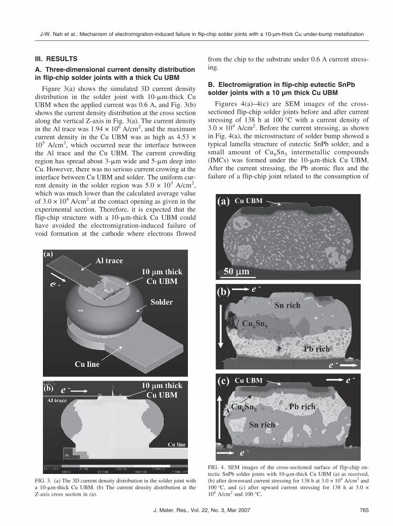
A 3D finite element model was constructed to simulatethe structure and current density distribution in the flip-chip solder joint as illustrated in Fig. 2. The model usedin this study was SOLID69 8-node hexahedral coupledfield element using Ansys simulation software (AnsysInc., Canonsburg, PA). The dimension of the mesh was3.8 �m. A detailed description of the simulation can befound elsewhere.12 The resistivities of the materials usedin the simulation are listed in Table I.
TABLE I. The resistivities of the materials used in the simulationmodels.
Materials Resistivity (�� cm)
Al 4.3TiW 70Cu 1.7Cu6Sn5 IMC 17.5Eutectic SnPb 14.6Ni3Sn4 IMC 28.5Ni 6.8
FIG. 2. The 3D finite element model showing the meshes in a solderjoint.
FIG. 1. Schematic diagram of the electromigration test sample.
J-W. Nah et al.: Mechanism of electromigration-induced failure in flip-chip solder joints with a 10-µm-thick Cu under-bump metallization
J. Mater. Res., Vol. 22, No. 3, Mar 2007764
III. RESULTS
A. Three-dimensional current density distributionin flip-chip solder joints with a thick Cu UBM
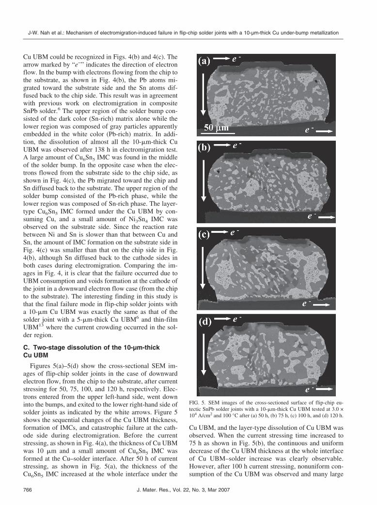
Figure 3(a) shows the simulated 3D current densitydistribution in the solder joint with 10-�m-thick CuUBM when the applied current was 0.6 A, and Fig. 3(b)shows the current density distribution at the cross sectionalong the vertical Z-axis in Fig. 3(a). The current densityin the Al trace was 1.94 × 10⁶ A/cm2, and the maximumcurrent density in the Cu UBM was as high as 4.53 ×10⁵ A/cm2, which occurred near the interface betweenthe Al trace and the Cu UBM. The current crowdingregion has spread about 3-�m wide and 5-�m deep intoCu. However, there was no serious current crowing at theinterface between Cu UBM and solder. The uniform cur-rent density in the solder region was 5.0 × 10³ A/cm2,which was much lower than the calculated average valueof 3.0 × 10⁴ A/cm2 at the contact opening as given in theexperimental section. Therefore, it is expected that theflip-chip structure with a 10-�m-thick Cu UBM couldhave avoided the electromigration-induced failure ofvoid formation at the cathode where electrons flowed
from the chip to the substrate under 0.6 A current stress-ing.
B. Electromigration in flip-chip eutectic SnPbsolder joints with a 10 µm thick Cu UBM
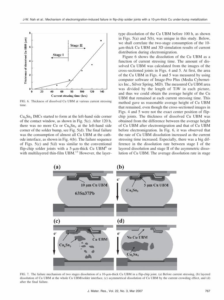
Figures 4(a)–4(c) are SEM images of the cross-sectioned flip-chip solder joints before and after currentstressing of 138 h at 100 °C with a current density of3.0 × 104 A/cm2. Before the current stressing, as shownin Fig. 4(a), the microstructure of solder bump showed atypical lamella structure of eutectic SnPb solder, and asmall amount of Cu6Sn5 intermetallic compounds(IMCs) was formed under the 10-�m-thick Cu UBM.After the current stressing, the Pb atomic flux and thefailure of a flip-chip joint related to the consumption of
FIG. 3. (a) The 3D current density distribution in the solder joint witha 10-�m-thick Cu UBM. (b) The current density distribution at theZ-axis cross section in (a).
FIG. 4. SEM images of the cross-sectioned surface of flip-chip eu-tectic SnPb solder joints with 10-�m-thick Cu UBM (a) as received,(b) after downward current stressing for 138 h at 3.0 × 10⁴ A/cm2 and100 °C, and (c) after upward current stressing for 138 h at 3.0 ×10⁴ A/cm2 and 100 °C.
J-W. Nah et al.: Mechanism of electromigration-induced failure in flip-chip solder joints with a 10-µm-thick Cu under-bump metallization
J. Mater. Res., Vol. 22, No. 3, Mar 2007 765
Cu UBM could be recognized in Figs. 4(b) and 4(c). Thearrow marked by “e−” indicates the direction of electronflow. In the bump with electrons flowing from the chip tothe substrate, as shown in Fig. 4(b), the Pb atoms mi-grated toward the substrate side and the Sn atoms dif-fused back to the chip side. This result was in agreementwith previous work on electromigration in compositeSnPb solder.6 The upper region of the solder bump con-sisted of the dark color (Sn-rich) matrix alone while thelower region was composed of gray particles apparentlyembedded in the white color (Pb-rich) matrix. In addi-tion, the dissolution of almost all the 10-�m-thick CuUBM was observed after 138 h in electromigration test.A large amount of Cu6Sn5 IMC was found in the middleof the solder bump. In the opposite case when the elec-trons flowed from the substrate side to the chip side, asshown in Fig. 4(c), the Pb migrated toward the chip andSn diffused back to the substrate. The upper region of thesolder bump consisted of the Pb-rich phase, while thelower region was composed of Sn-rich phase. The layer-type Cu6Sn5 IMC formed under the Cu UBM by con-suming Cu, and a small amount of Ni3Sn4 IMC wasobserved on the substrate side. Since the reaction ratebetween Ni and Sn is slower than that between Cu andSn, the amount of IMC formation on the substrate side inFig. 4(c) was smaller than that on the chip side in Fig.4(b), although Sn diffused back to the cathode sides inboth cases during electromigration. Comparing the im-ages in Fig. 4, it is clear that the failure occurred due toUBM consumption and voids formation at the cathode ofthe joint in a downward electron flow case (from the chipto the substrate). The interesting finding in this study isthat the final failure mode in flip-chip solder joints witha 10-�m Cu UBM was exactly the same as that of thesolder joint with a 5-�m-thick Cu UBM6 and thin-filmUBM13 where the current crowding occurred in the sol-der region.
C. Two-stage dissolution of the 10-µm-thickCu UBM
Figures 5(a)–5(d) show the cross-sectional SEM im-ages of flip-chip solder joints in the case of downwardelectron flow, from the chip to the substrate, after currentstressing for 50, 75, 100, and 120 h, respectively. Elec-trons entered from the upper left-hand side, went downinto the bumps, and exited to the lower right-hand side ofsolder joints as indicated by the white arrows. Figure 5shows the sequential changes of the Cu UBM thickness,formation of IMCs, and catastrophic failure at the cath-ode side during electromigration. Before the currentstressing, as shown in Fig. 4(a), the thickness of Cu UBMwas 10 �m and a small amount of Cu6Sn5 IMC wasformed at the Cu–solder interface. After 50 h of currentstressing, as shown in Fig. 5(a), the thickness of theCu6Sn5 IMC increased at the whole interface under the
Cu UBM, and the layer-type dissolution of Cu UBM wasobserved. When the current stressing time increased to75 h as shown in Fig. 5(b), the continuous and uniformdecrease of the Cu UBM thickness at the whole interfaceof Cu UBM–solder increase was clearly observable.However, after 100 h current stressing, nonuniform con-sumption of the Cu UBM was observed and many large
FIG. 5. SEM images of the cross-sectioned surface of flip-chip eu-tectic SnPb solder joints with a 10-�m-thick Cu UBM tested at 3.0 ×10⁴ A/cm2 and 100 °C after (a) 50 h, (b) 75 h, (c) 100 h, and (d) 120 h.
J-W. Nah et al.: Mechanism of electromigration-induced failure in flip-chip solder joints with a 10-µm-thick Cu under-bump metallization
J. Mater. Res., Vol. 22, No. 3, Mar 2007766
Cu6Sn5 IMCs started to form at the left-hand side cornerof the contact window, as shown in Fig. 5(c). After 120 h,there was no more Cu or Cu6Sn5 at the left-hand sidecorner of the solder bump, see Fig. 5(d). The final failurewas the consumption of almost all Cu UBM at the cath-ode interface, as shown in Fig. 4(b). The failure sequenceof Figs. 5(c) and 5(d) was similar to the conventionalflip-chip solder joints with a 5-�m-thick Cu UBM6 orwith multilayered thin-film UBM.13 However, the layer-
type dissolution of the Cu UBM before 100 h, as shownin Figs. 5(a) and 5(b), was unique in this study. Below,we shall correlate the two-stage consumption of the 10-�m-thick Cu UBM and 3D simulation results of currentdistribution during electromigration.
Figure 6 shows the dissolution of the Cu UBM as afunction of current stressing time. The amount of dis-solved Cu UBM was calculated from the images of thecross-sectioned joints in Figs. 4 and 5. At first, the areaof the Cu UBM in Figs. 4 and 5 was measured by usingcomputer software of Image-Pro Plus (Media Cybernet-ics Inc., Silver Spring, MD). The measured Cu UBM areawas divided by the length of TiW in each picture,and thus we could obtain the average height of the CuUBM that remained at each current stressing time. Thismethod gave us reasonable average height of Cu UBMthat remained, even though the cross-sectioned images inFigs. 4 and 5 were not the exact center position of flip-chip joints. The thickness of dissolved Cu UBM wasobtained from the difference between the average heightof Cu UBM after electromigration and that of Cu UBMbefore electromigration. In Fig. 6, it was observed thatthe rate of Cu UBM dissolution increased as the currentstressing time increased. Especially, there was a big dif-ference in the dissolution rate between stage I of thelayered dissolution and stage II of the asymmetric disso-lution of Cu UBM. The average dissolution rate in stage
FIG. 6. Thickness of dissolved Cu UBM at various current stressingtime.
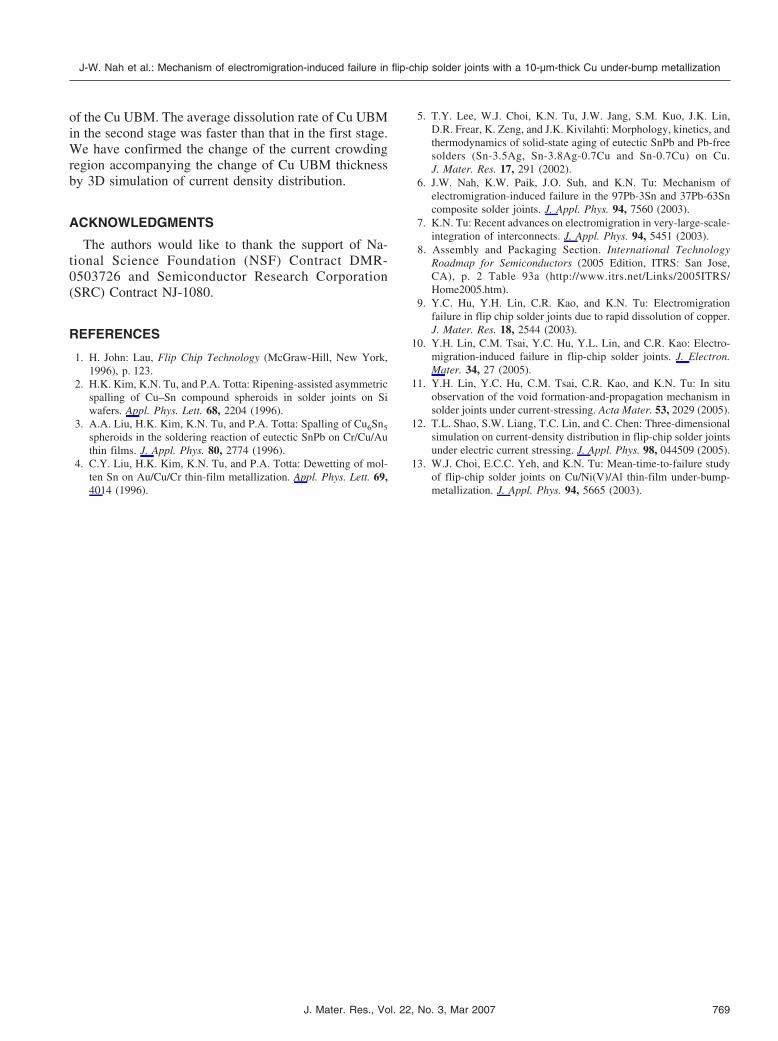
FIG. 7. The failure mechanism of two stages dissolution of a 10-�m-thick Cu UBM in a flip-chip joint. (a) Before current stressing, (b) layereddissolution of Cu UBM at the whole Cu UBM/solder interface, (c) asymmetrical dissolution of Cu UBM by the current crowding effect, and (d)after the final failure.
J-W. Nah et al.: Mechanism of electromigration-induced failure in flip-chip solder joints with a 10-µm-thick Cu under-bump metallization
J. Mater. Res., Vol. 22, No. 3, Mar 2007 767
I was 0.0175 �m/h and that in stage II was 0.0892 �m/h.The origin of this accelerated dissolution in stage II wasfrom the current crowding effect discussed in the nextsection. The current crowding at the Cu UBM–solderinterface enhanced the reaction between Cu and Sn andaccelerated the consumption of Cu UBM to form theCu6Sn5 IMC.
IV. DISCUSSION
A possible mechanism for the two-stage dissolution ofthe 10-�m-thick Cu UBM under low current density, i.e.,the current crowding area located inside the UBM isillustrated in Fig. 7. As shown in Fig. 7(a), the flip-chipsolder joint had 10-�m-thick Cu UBM before currentstressing. In the initial stage of electromigration, sincethe thickness of Cu UBM was thick enough to contain thecurrent crowding region inside Cu UBM, the current dis-tribution at the entire Cu UBM–solder interface was uni-form and resulted in the layer-type dissolution of the CuUBM, as shown in Fig. 7(b). However, as the thicknessof the Cu UBM decreased with increasing time of currentstressing, the effect of current crowding on the nonuni-form current distribution at the Cu UBM–solder interfaceincreased, especially at the location where the electronsflowed into the solder bump. The current crowding droveCu atoms from the upper left-hand side corner toward theanode and accelerated the formation of Cu6Sn5 IMC atthe upper left-hand side corner as shown in Fig. 7(c). Theformation of Cu6Sn5 IMC was greatly enhanced as thetime increased, and finally the dissolution of Cu6Sn5
IMC into the solder induced the failure in the flip-chipjoint as depicted in Fig. 7(d).
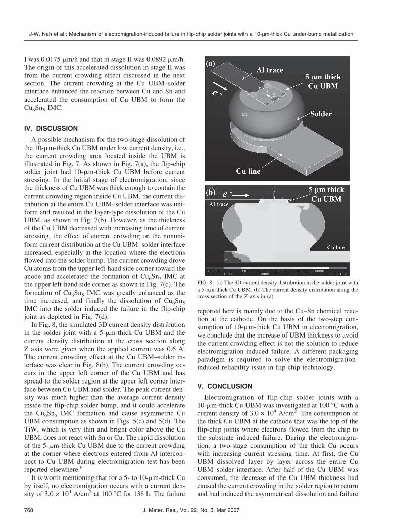
In Fig. 8, the simulated 3D current density distributionin the solder joint with a 5-�m-thick Cu UBM and thecurrent density distribution at the cross section alongZ axis were given when the applied current was 0.6 A.The current crowding effect at the Cu UBM–solder in-terface was clear in Fig. 8(b). The current crowding oc-curs in the upper left corner of the Cu UBM and hasspread to the solder region at the upper left corner inter-face between Cu UBM and solder. The peak current den-sity was much higher than the average current densityinside the flip-chip solder bump, and it could acceleratethe Cu6Sn5 IMC formation and cause asymmetric CuUBM consumption as shown in Figs. 5(c) and 5(d). TheTiW, which is very thin and bright color above the CuUBM, does not react with Sn or Cu. The rapid dissolutionof the 5-�m-thick Cu UBM due to the current crowdingat the corner where electrons entered from Al intercon-nect to Cu UBM during electromigration test has beenreported elsewhere.6
It is worth mentioning that for a 5- to 10-�m-thick Cuby itself, no electromigration occurs with a current den-sity of 3.0 × 10⁴ A/cm2 at 100 °C for 138 h. The failure
reported here is mainly due to the Cu–Sn chemical reac-tion at the cathode. On the basis of the two-step con-sumption of 10-�m-thick Cu UBM in electromigration,we conclude that the increase of UBM thickness to avoidthe current crowding effect is not the solution to reduceelectromigration-induced failure. A different packagingparadigm is required to solve the electromigration-induced reliability issue in flip-chip technology.
V. CONCLUSION
Electromigration of flip-chip solder joints with a10-�m-thick Cu UBM was investigated at 100 °C with acurrent density of 3.0 × 10⁴ A/cm2. The consumption ofthe thick Cu UBM at the cathode that was the top of theflip-chip joints where electrons flowed from the chip tothe substrate induced failure. During the electromigra-tion, a two-stage consumption of the thick Cu occurswith increasing current stressing time. At first, the CuUBM dissolved layer by layer across the entire CuUBM–solder interface. After half of the Cu UBM wasconsumed, the decrease of the Cu UBM thickness hadcaused the current crowding in the solder region to returnand had induced the asymmetrical dissolution and failure
FIG. 8. (a) The 3D current density distribution in the solder joint witha 5-�m-thick Cu UBM. (b) The current density distribution along thecross section of the Z-axis in (a).
J-W. Nah et al.: Mechanism of electromigration-induced failure in flip-chip solder joints with a 10-µm-thick Cu under-bump metallization
J. Mater. Res., Vol. 22, No. 3, Mar 2007768
of the Cu UBM. The average dissolution rate of Cu UBMin the second stage was faster than that in the first stage.We have confirmed the change of the current crowdingregion accompanying the change of Cu UBM thicknessby 3D simulation of current density distribution.
ACKNOWLEDGMENTS
The authors would like to thank the support of Na-tional Science Foundation (NSF) Contract DMR-0503726 and Semiconductor Research Corporation(SRC) Contract NJ-1080.
REFERENCES
1. H. John: Lau, Flip Chip Technology (McGraw-Hill, New York,1996), p. 123.
2. H.K. Kim, K.N. Tu, and P.A. Totta: Ripening-assisted asymmetricspalling of Cu–Sn compound spheroids in solder joints on Siwafers. Appl. Phys. Lett. 68, 2204 (1996).
3. A.A. Liu, H.K. Kim, K.N. Tu, and P.A. Totta: Spalling of Cu6Sn5
spheroids in the soldering reaction of eutectic SnPb on Cr/Cu/Authin films. J. Appl. Phys. 80, 2774 (1996).
4. C.Y. Liu, H.K. Kim, K.N. Tu, and P.A. Totta: Dewetting of mol-ten Sn on Au/Cu/Cr thin-film metallization. Appl. Phys. Lett. 69,4014 (1996).
5. T.Y. Lee, W.J. Choi, K.N. Tu, J.W. Jang, S.M. Kuo, J.K. Lin,D.R. Frear, K. Zeng, and J.K. Kivilahti: Morphology, kinetics, andthermodynamics of solid-state aging of eutectic SnPb and Pb-freesolders (Sn-3.5Ag, Sn-3.8Ag-0.7Cu and Sn-0.7Cu) on Cu.J. Mater. Res. 17, 291 (2002).
6. J.W. Nah, K.W. Paik, J.O. Suh, and K.N. Tu: Mechanism ofelectromigration-induced failure in the 97Pb-3Sn and 37Pb-63Sncomposite solder joints. J. Appl. Phys. 94, 7560 (2003).
7. K.N. Tu: Recent advances on electromigration in very-large-scale-integration of interconnects. J. Appl. Phys. 94, 5451 (2003).
8. Assembly and Packaging Section. International TechnologyRoadmap for Semiconductors (2005 Edition, ITRS: San Jose,CA), p. 2 Table 93a (http://www.itrs.net/Links/2005ITRS/Home2005.htm).
9. Y.C. Hu, Y.H. Lin, C.R. Kao, and K.N. Tu: Electromigrationfailure in flip chip solder joints due to rapid dissolution of copper.J. Mater. Res. 18, 2544 (2003).
10. Y.H. Lin, C.M. Tsai, Y.C. Hu, Y.L. Lin, and C.R. Kao: Electro-migration-induced failure in flip-chip solder joints. J. Electron.Mater. 34, 27 (2005).
11. Y.H. Lin, Y.C. Hu, C.M. Tsai, C.R. Kao, and K.N. Tu: In situobservation of the void formation-and-propagation mechanism insolder joints under current-stressing. Acta Mater. 53, 2029 (2005).
12. T.L. Shao, S.W. Liang, T.C. Lin, and C. Chen: Three-dimensionalsimulation on current-density distribution in flip-chip solder jointsunder electric current stressing. J. Appl. Phys. 98, 044509 (2005).
13. W.J. Choi, E.C.C. Yeh, and K.N. Tu: Mean-time-to-failure studyof flip-chip solder joints on Cu/Ni(V)/Al thin-film under-bump-metallization. J. Appl. Phys. 94, 5665 (2003).
J-W. Nah et al.: Mechanism of electromigration-induced failure in flip-chip solder joints with a 10-µm-thick Cu under-bump metallization
J. Mater. Res., Vol. 22, No. 3, Mar 2007 769