Embed Size (px)
Citation preview
Texas Instruments 1 AAJ 4Q 2016
IndustrialAnalog Applications Journal
Measuring the linear operating region of instrumentation amplifiers
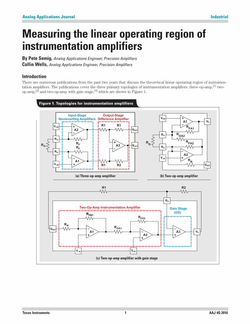
IntroductionThere are numerous publications from the past two years that discuss the theoretical linear operating region of instrumen-tation amplifiers. The publications cover the three primary topologies of instrumentation amplifiers: three-op-amp,[1] two-op-amp,[2] and two-op-amp with gain stage,[3] which are shown in Figure 1.
By Pete Semig, Analog Applications Engineer, Precision AmplifiersCollin Wells, Analog Applications Engineer, Precision Amplifiers
Figure 1. Topologies for instrumentation amplifiers
A3 VOUT
V+IN
V–IN
RG
RG
RGRF
R1
R1
R1
R2
RF
A2
A1
VREF
Input-StageNoninverting Amplifiers
Output-StageDifference Amplifier
+
+
+
–
–
–
VO
VREF
V+IN
V–IN
RG
RGRG
A1
A2
RFA2
RR
RFA1
ROA2
+
+
–
–
R1 R2
Two-Op-Amp Instrumentation Amplifier Gain Stage
(GS)
VO
VREF
RR
A1A2
A3+
++
––
–
V+INV–IN
ROA1
RFA1RFA1RFA2
RG
(a) Three-op-amp amplifier (b) Two-op-amp amplifier
(c) Two-op-amp amplifier with gain stage
Texas Instruments 2 AAJ 4Q 2016
IndustrialAnalog Applications Journal
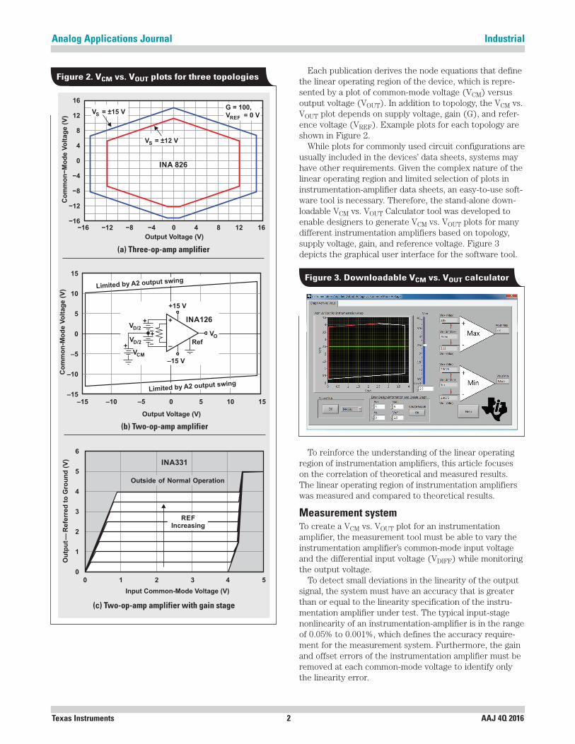
Each publication derives the node equations that define the linear operating region of the device, which is repre-sented by a plot of common-mode voltage (VCM) versus output voltage (VOUT). In addition to topology, the VCM vs. VOUT plot depends on supply voltage, gain (G), and refer-ence voltage (VREF). Example plots for each topology are shown in Figure 2.
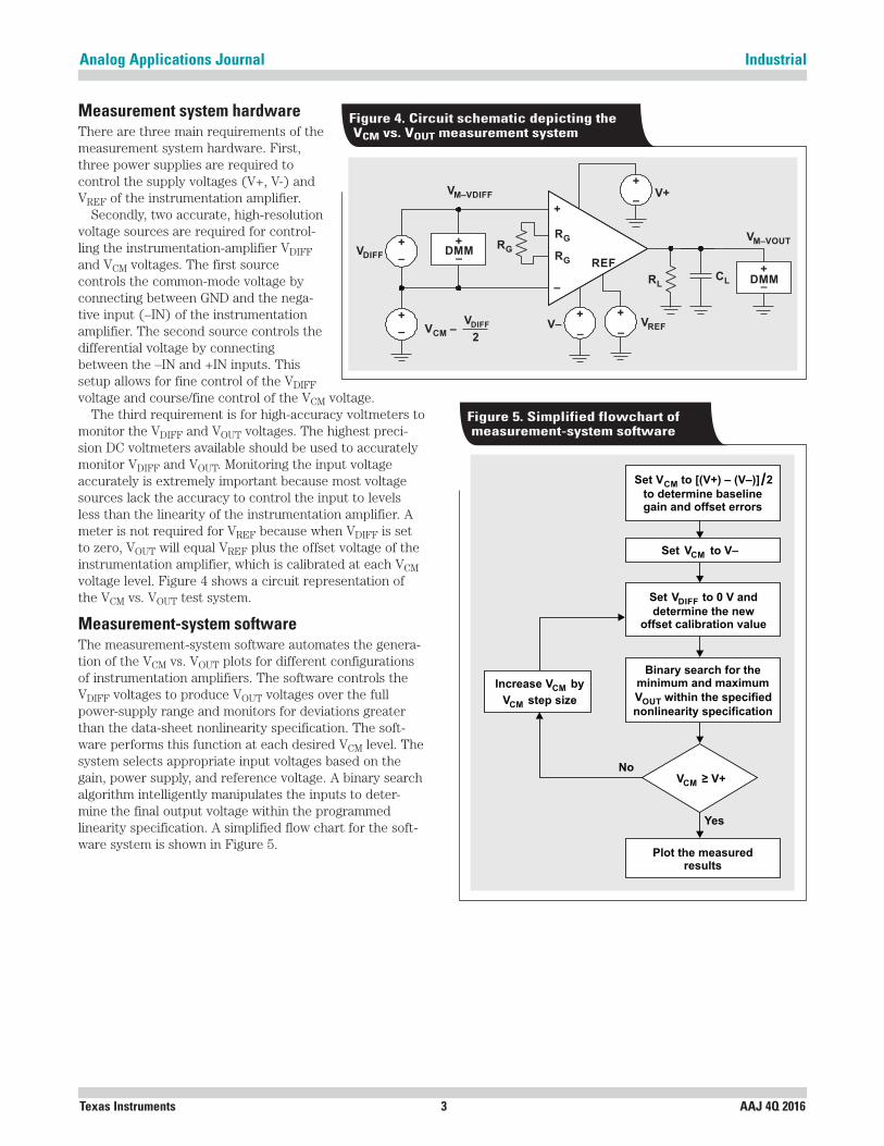
While plots for commonly used circuit configurations are usually included in the devices’ data sheets, systems may have other requirements. Given the complex nature of the linear operating region and limited selection of plots in instrumentation-amplifier data sheets, an easy-to-use soft-ware tool is necessary. Therefore, the stand-alone down-loadable VCM vs. VOUT Calculator tool was developed to enable designers to generate VCM vs. VOUT plots for many different instrumentation amplifiers based on topology, supply voltage, gain, and reference voltage. Figure 3 depicts the graphical user interface for the software tool.
Figure 2. VCM vs. VOUT plots for three topologies
−16
−12
−8
−4
0
4
8
12
16
−16 −12 −8 −4 0 4 8 12 16
Co
mm
on
−M
od
e V
olt
ag
e (
V)
G = 100,V = 0 VREF
V = ±15 VS
V = ±12 VS
Output Voltage (V)
INA 826
Output Voltage (V)
Co
mm
on
-Mo
de V
olt
ag
e (
V)
–15 –10 0 5 15–5
15
10
5
0
–5
–10
–1510
VD/2
VD/2
+
+–
–
VCM
VO
Ref
–15 V
+15 V
+
–+
Limited by A2 output swing
Limited by A2 output swing
INA126
0
Ou
tpu
t—R
efe
rre
d t
o G
rou
nd
(V
)
Input Common-Mode Voltage (V)
1 2 3 4 5
6
5
4
3
2
1
0
INA331
REFIncreasing
Outside of Normal Operation
(a) Three-op-amp amplifier
(b) Two-op-amp amplifier
(c) Two-op-amp amplifier with gain stage
Figure 3. Downloadable VCM vs. VOUT calculator
To reinforce the understanding of the linear operating region of instrumentation amplifiers, this article focuses on the correlation of theoretical and measured results. The linear operating region of instrumentation amplifiers was measured and compared to theoretical results.
Measurement systemTo create a VCM vs. VOUT plot for an instrumentation amplifier, the measurement tool must be able to vary the instrumentation amplifier’s common-mode input voltage and the differential input voltage (VDIFF) while monitoring the output voltage.
To detect small deviations in the linearity of the output signal, the system must have an accuracy that is greater than or equal to the linearity specification of the instru-mentation amplifier under test. The typical input-stage nonlinearity of an instrumentation-amplifier is in the range of 0.05% to 0.001%, which defines the accuracy require-ment for the measurement system. Furthermore, the gain and offset errors of the instrumentation amplifier must be removed at each common-mode voltage to identify only the linearity error.
Texas Instruments 3 AAJ 4Q 2016
IndustrialAnalog Applications Journal
Measurement system hardwareThere are three main requirements of the measurement system hardware. First, three power supplies are required to control the supply voltages (V+, V-) and VREF of the instrumentation amplifier.
Secondly, two accurate, high-resolution voltage sources are required for control-ling the instrumentation-amplifier VDIFF and VCM voltages. The first source controls the common-mode voltage by connecting between GND and the nega-tive input (–IN) of the instrumentation amplifier. The second source controls the differential voltage by connecting between the –IN and +IN inputs. This setup allows for fine control of the VDIFF voltage and course/fine control of the VCM voltage.
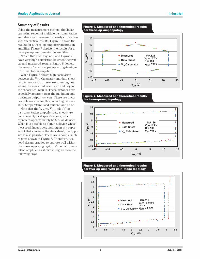
The third requirement is for high-accuracy voltmeters to monitor the VDIFF and VOUT voltages. The highest preci-sion DC voltmeters available should be used to accurately monitor VDIFF and VOUT. Monitoring the input voltage accurately is extremely important because most voltage sources lack the accuracy to control the input to levels less than the linearity of the instrumentation amplifier. A meter is not required for VREF because when VDIFF is set to zero, VOUT will equal VREF plus the offset voltage of the instrumentation amplifier, which is calibrated at each VCM voltage level. Figure 4 shows a circuit representation of the VCM vs. VOUT test system.
Measurement-system softwareThe measurement-system software automates the genera-tion of the VCM vs. VOUT plots for different configurations of instrumentation amplifiers. The software controls the VDIFF voltages to produce VOUT voltages over the full power-supply range and monitors for deviations greater than the data-sheet nonlinearity specification. The soft-ware performs this function at each desired VCM level. The system selects appropriate input voltages based on the gain, power supply, and reference voltage. A binary search algorithm intelligently manipulates the inputs to deter-mine the final output voltage within the programmed linearity specification. A simplified flow chart for the soft-ware system is shown in Figure 5.
Figure 4. Circuit schematic depicting the VCM vs. VOUT measurement system
REF
+
–V+
V–+
–VREF
+
–
+
– –
+
–
VDIFF
VM–VDIFF
VM–VOUT
–
+
RG
RLCL
RG
RG
+DMM
+
–DMM
VDIFF
2V –CM
Figure 5. Simplified flowchart of measurement-system software
Set V to 0 V andDIFF
determine the newoffset calibration value
Binary search for theminimum and maximum
V within the specifiedOUT
nonlinearity specification
V ≥ V+CM
Increase V byCM
V step sizeCM
Plot the measuredresults
No
Yes
Set V to [(V+) – (V–)] 2CM /to determine baselinegain and offset errors
Set V to V–CM
Texas Instruments 4 AAJ 4Q 2016
IndustrialAnalog Applications Journal
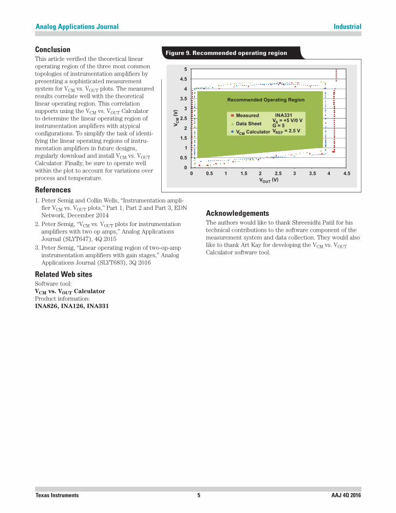
Summary of ResultsUsing the measurement system, the linear operating region of multiple instrumentation amplifiers was measured to verify correlation with theoretical results. Figure 6 shows the results for a three-op-amp instrumentation amplifier. Figure 7 depicts the results for a two-op-amp instrumentation amplifier.
Notice that both Figure 6 and Figure 7 have very high correlation between theoreti-cal and measured results. Figure 8 depicts the results for a two-op-amp with gain-stage instrumentation amplifier.
While Figure 8 shows high correlation between the VCM Calculator and data-sheet results, notice that there are some regions where the measured results extend beyond the theoretical results. These instances are especially apparent near the minimum and maximum output voltages. There are many possible reasons for this, including process shift, temperature, load current, and so on.
Note that the VCM vs. VOUT plot(s) in instrumentation-amplifier data sheets are considered typical specifications, which represent approximately 68% of all devices. While it is possible to obtain a device whose measured linear operating region is a super-set of that shown in the data sheet, the oppo-site is also possible. There are a couple such regions shown in Figure 8. Therefore, it is good design practice to operate well within the linear operating region of the instrumen-tation amplifier as shown in Figure 9 on the following page.
Figure 6. Measured and theoretical results for three-op-amp topology
–15
–10
–10 10 15–5 0 5–15
–5
0
5
10
15
INA826V = ±12 VSG = 100V = 0 VREF
Measured
Data Sheet
V CalculatorCM
V (V)CM
V( V
)O
UT
Figure 7. Measured and theoretical results for two-op-amp topology
–15
–10
–10 10 15–5 0 5–15
–5
0
5
10
15
INA126V = ±15 VS
G = 100V = 0 VREF
Measured
Data Sheet
V CalculatorCM
V (V)OUT
V( V
)C
M
Figure 8. Measured and theoretical results for two-op-amp with gain-stage topology
0
0.5
1
1.5
2
2.5
3
3.5
4
4.5
5
0 0.5 1 1.5 2 2.5 3 3.5 4 4.5
V( V
)C
M
V (V)OUT
INA331V = +5 V/0 VSG = 5V = 2.5 VREF
Measured
Data Sheet
V CalculatorCM
Texas Instruments 5 AAJ 4Q 2016
IndustrialAnalog Applications Journal
ConclusionThis article verified the theoretical linear operating region of the three most common topologies of instrumentation amplifiers by presenting a sophisticated measurement system for VCM vs. VOUT plots. The measured results correlate well with the theoretical linear operating region. This correlation supports using the VCM vs. VOUT Calculator to determine the linear operating region of instrumentation amplifiers with atypical configurations. To simplify the task of identi-fying the linear operating regions of instru-mentation amplifiers in future designs, regularly download and install VCM vs. VOUT Calculator. Finally, be sure to operate well within the plot to account for variations over process and temperature.
References1. Peter Semig and Collin Wells, “Instrumentation ampli-
fier VCM vs. VOUT plots,” Part 1, Part 2 and Part 3, EDN Network, December 2014
2. Peter Semig, “VCM vs. VOUT plots for instrumentation amplifiers with two op amps,” Analog Applications Journal (SLYT647), 4Q 2015
3. Peter Semig, “Linear operating region of two-op-amp instrumentation amplifiers with gain stages,” Analog Applications Journal (SLYT683), 3Q 2016
Related Web sitesSoftware tool:VCM vs. VOUT CalculatorProduct information:INA826, INA126, INA331
Figure 9. Recommended operating region
0
0.5
1
1.5
2
2.5
3
3.5
4
4.5
5
0 0.5 1 1.5 2 2.5 3 3.5 4 4.5V
( V)
CM
V (V)OUT
INA331V = +5 V/0 VSG = 5V = 2.5 VREF
Measured
Data Sheet
V CalculatorCM
Recommended Operating Region
AcknowledgementsThe authors would like to thank Shreenidhi Patil for his technical contributions to the software component of the measurement system and data collection. They would also like to thank Art Kay for developing the VCM vs. VOUT Calculator software tool.
Texas Instruments 6 AAJ 4Q 2016
Analog Applications Journal
E2E is a trademark of Texas Instruments. All other trademarks are the property of their respective owners.
TI Worldwide Technical Support
InternetTI Semiconductor Product Information Center Home Pagesupport.ti.com
TI E2E™ Community Home Pagee2e.ti.com
Product Information CentersAmericas Phone +1(512) 434-1560
Brazil Phone 0800-891-2616
Mexico Phone 0800-670-7544
Fax +1(972) 927-6377 Internet/Email support.ti.com/sc/pic/americas.htm
Europe, Middle East, and AfricaPhone European Free Call 00800-ASK-TEXAS (00800 275 83927) International +49 (0) 8161 80 2121 Russian Support +7 (4) 95 98 10 701
Note: The European Free Call (Toll Free) number is not active in all countries. If you have technical difficulty calling the free call number, please use the international number above.
Fax +(49) (0) 8161 80 2045Internet www.ti.com/asktexasDirect Email [email protected]
JapanFax International +81-3-3344-5317 Domestic 0120-81-0036
Internet/Email International support.ti.com/sc/pic/japan.htm Domestic www.tij.co.jp/pic
AsiaPhone Toll-Free Number Note: Toll-free numbers may not support
mobile and IP phones. Australia 1-800-999-084 China 800-820-8682 Hong Kong 800-96-5941 India 000-800-100-8888 Indonesia 001-803-8861-1006 Korea 080-551-2804 Malaysia 1-800-80-3973 New Zealand 0800-446-934 Philippines 1-800-765-7404 Singapore 800-886-1028 Taiwan 0800-006800 Thailand 001-800-886-0010International +86-21-23073444Fax +86-21-23073686Email [email protected] or [email protected] support.ti.com/sc/pic/asia.htm
A021014
Important Notice: The products and services of Texas Instruments Incorporated and its subsidiaries described herein are sold subject to TI’s standard terms and conditions of sale. Customers are advised to obtain the most current and complete information about TI products and services before placing orders. TI assumes no liability for applications assistance, customer’s applications or product designs, software performance, or infringement of patents. The publication of information regarding any other company’s products or services does not constitute TI’s approval, warranty or endorsement thereof.
© 2016 Texas Instruments Incorporated. All rights reserved. SLYT690
IMPORTANT NOTICE
Texas Instruments Incorporated and its subsidiaries (TI) reserve the right to make corrections, enhancements, improvements and otherchanges to its semiconductor products and services per JESD46, latest issue, and to discontinue any product or service per JESD48, latestissue. Buyers should obtain the latest relevant information before placing orders and should verify that such information is current andcomplete. All semiconductor products (also referred to herein as “components”) are sold subject to TI’s terms and conditions of salesupplied at the time of order acknowledgment.TI warrants performance of its components to the specifications applicable at the time of sale, in accordance with the warranty in TI’s termsand conditions of sale of semiconductor products. Testing and other quality control techniques are used to the extent TI deems necessaryto support this warranty. Except where mandated by applicable law, testing of all parameters of each component is not necessarilyperformed.TI assumes no liability for applications assistance or the design of Buyers’ products. Buyers are responsible for their products andapplications using TI components. To minimize the risks associated with Buyers’ products and applications, Buyers should provideadequate design and operating safeguards.TI does not warrant or represent that any license, either express or implied, is granted under any patent right, copyright, mask work right, orother intellectual property right relating to any combination, machine, or process in which TI components or services are used. Informationpublished by TI regarding third-party products or services does not constitute a license to use such products or services or a warranty orendorsement thereof. Use of such information may require a license from a third party under the patents or other intellectual property of thethird party, or a license from TI under the patents or other intellectual property of TI.Reproduction of significant portions of TI information in TI data books or data sheets is permissible only if reproduction is without alterationand is accompanied by all associated warranties, conditions, limitations, and notices. TI is not responsible or liable for such altereddocumentation. Information of third parties may be subject to additional restrictions.Resale of TI components or services with statements different from or beyond the parameters stated by TI for that component or servicevoids all express and any implied warranties for the associated TI component or service and is an unfair and deceptive business practice.TI is not responsible or liable for any such statements.Buyer acknowledges and agrees that it is solely responsible for compliance with all legal, regulatory and safety-related requirementsconcerning its products, and any use of TI components in its applications, notwithstanding any applications-related information or supportthat may be provided by TI. Buyer represents and agrees that it has all the necessary expertise to create and implement safeguards whichanticipate dangerous consequences of failures, monitor failures and their consequences, lessen the likelihood of failures that might causeharm and take appropriate remedial actions. Buyer will fully indemnify TI and its representatives against any damages arising out of the useof any TI components in safety-critical applications.In some cases, TI components may be promoted specifically to facilitate safety-related applications. With such components, TI’s goal is tohelp enable customers to design and create their own end-product solutions that meet applicable functional safety standards andrequirements. Nonetheless, such components are subject to these terms.No TI components are authorized for use in FDA Class III (or similar life-critical medical equipment) unless authorized officers of the partieshave executed a special agreement specifically governing such use.Only those TI components which TI has specifically designated as military grade or “enhanced plastic” are designed and intended for use inmilitary/aerospace applications or environments. Buyer acknowledges and agrees that any military or aerospace use of TI componentswhich have not been so designated is solely at the Buyer's risk, and that Buyer is solely responsible for compliance with all legal andregulatory requirements in connection with such use.TI has specifically designated certain components as meeting ISO/TS16949 requirements, mainly for automotive use. In any case of use ofnon-designated products, TI will not be responsible for any failure to meet ISO/TS16949.
Products ApplicationsAudio www.ti.com/audio Automotive and Transportation www.ti.com/automotiveAmplifiers amplifier.ti.com Communications and Telecom www.ti.com/communicationsData Converters dataconverter.ti.com Computers and Peripherals www.ti.com/computersDLP® Products www.dlp.com Consumer Electronics www.ti.com/consumer-appsDSP dsp.ti.com Energy and Lighting www.ti.com/energyClocks and Timers www.ti.com/clocks Industrial www.ti.com/industrialInterface interface.ti.com Medical www.ti.com/medicalLogic logic.ti.com Security www.ti.com/securityPower Mgmt power.ti.com Space, Avionics and Defense www.ti.com/space-avionics-defenseMicrocontrollers microcontroller.ti.com Video and Imaging www.ti.com/videoRFID www.ti-rfid.comOMAP Applications Processors www.ti.com/omap TI E2E Community e2e.ti.comWireless Connectivity www.ti.com/wirelessconnectivity
Mailing Address: Texas Instruments, Post Office Box 655303, Dallas, Texas 75265Copyright © 2016, Texas Instruments Incorporated