Embed Size (px)
Citation preview

MEASUREMENT OF ‘ONE OVER F NOISE’ IN INFRARED
DETECTION USING A NOVEL TECHNIQUE
BY
DIANA MAESTAS JEPSON
B.S., ELECTRICAL ENGINEERING, UNIVERSITY OF NEW MEXICO, 2001
THESIS
Submitted in Partial Fulfillment of the Requirements for the Degree of
Master of Science
Electrical Engineering
The University of New Mexico Albuquerque, New Mexico
July 2007
iii
DEDICATION
This thesis is dedicated to my husband and son, who were my inspiration for
continuing to move forward with my education. I would also like to dedicate it to my
mother and father. Thank all of you for your love, patience, encouragement, support and
prayers.
iv
ACKNOWLEDGEMENTS
This project would not have been possible without the support of many people.
Many thanks to my advisor and committee chair, Dr. Sanjay Krishna, who helped and
guided me throughout the time it took me to complete this research and write the thesis.
Also thanks to my committee members, Dr. Kevin Malloy and Dr. DanHong Huang, who
have generously given their time and expertise to better my work. I thank them for their
contribution and their good-natured support.
I must acknowledge as well my colleagues who assisted, advised, and supported
my research over the years. Thank you to Dr. John E. Hubbs, Mark E. Gramer, and Gary
Dole for their support and expertise in the laboratory. Their support of this project was
greatly needed and deeply appreciated. A special thanks to Dr. Hubbs who generously
shared his meticulous research and insights that supported and expanded my own work.
Thank you to Amber Anderson, Dr. Paul Levan and Dr. Yolanda King, from the Space
Vehicles Directorate, Air Force Research Laboratory for their critical review of this
thesis and ensuring I was staying in between the lines. Also thanks to AFRL/VSSS, with
the support of Dr. Hubbs, for allowing me to complete this research through the Infrared
Radiation Effects Laboratory.
And finally, thanks to my husband, son and parents who endured this long process
with me, always offering support and love. I could not have completed this thesis
without all of your help.
MEASUREMENT OF ‘ONE OVER F NOISE’ IN INFRARED
DETECTION USING A NOVEL TECHNIQUE
BY
DIANA MAESTAS JEPSON
ABSTRACT OF THESIS
Submitted in Partial Fulfillment of the Requirements for the Degree of
Master of Science
Electrical Engineering
The University of New Mexico Albuquerque, New Mexico
July 2007
vi
Measurement Of ‘One Over F Noise’ In Infrared Detection Using A
Novel Technique
by
Diana Maestas Jepson
B.S., Electrical Engineering, University of New Mexico, 2001
M.S., Electrical Engineering, University of New Mexico, 2007
ABSTRACT
It has been shown that, ‘one over f noise’ (1/f noise) limits the sensitivity in
Mercury Cadmium Telluride (HgCdTe) infrared devices. It is therefore imperative to be
able to measure and account for its contribution to the total device noise. In this thesis,
the 1/f noise of a HgCdTe device is measured and studied using two measurement
techniques. The first technique is the commonly used conventional method of measuring
1/f noise that analyzes 1/f noise in the frequency domain and extracts the 1/f noise
contribution from the power spectral densities. The second approach is a novel technique
that extracts the 1/f noise contribution from the total measured noise data that is collected
as a function of integration time at a very low photon irradiance. By analyzing the 1/f
noise of this device using the conventional method, the results using this novel technique
can be compared and its accuracy validated. The advantages of the novel technique over
the conventional method result in a simpler method of measuring and analyzing 1/f noise
in these devices. First the data can be collected in a fairly short amount of time, as
compared to the conventional method where data must be collected for very long periods
vii
of time. As a result of collecting data for such long periods of time, the environment
must be extremely controlled such that drifts in temperature or the patience of the person
taking the measurements do not limit the accuracy of the results. In addition the data
analysis is also simplified using the novel technique.
This novel technique of measuring 1/f noise has been developed at the Infrared
Radiation Effects Laboratory (IRREL), Air Force Research Laboratory, Kirtland Air
Force Base and is studied and validated here in this thesis.
viii
TABLE OF CONTENTS
List of Figures _________________________________________________________ xi
List of Tables _________________________________________________________ xv
1 Introduction to HgCdTe Devices _______________________________________ 1
1.1 Outline and Layout of Thesis __________________________________________ 1
1.2 Importance of HgCdTe in Infrared Detection _____________________________ 2
1.3 Figures of Merit Used In Infrared Detection ______________________________ 5
1.3.1 Conversion Gain___________________________________________________________5
1.3.1.1 DC Current Method ___________________________________________________5
1.3.1.2 Mean Variance Method_________________________________________________8
1.3.2 Responsivity ______________________________________________________________8
1.3.3 Dark Current______________________________________________________________9
1.3.4 Detectivity (D*) __________________________________________________________10
1.3.5 Noise Equivalent Input (NEI)________________________________________________11
1.3.6 Noise Equivalent Power (NEP) ______________________________________________11
1.3.7 Noise Equivalent Temperature Difference (NETD)_______________________________12
1.4 Noise Sources ______________________________________________________ 14
1.4.1 Read Noise ______________________________________________________________14
ix
1.4.2 Thermal Noise ___________________________________________________________15
1.4.3 Generation Recombination Noise_____________________________________________15
1.4.4 Photon Noise ____________________________________________________________16
1.4.5 1/f Noise ________________________________________________________________17
1.5 1/f Noise in HgCdTe Devices __________________________________________ 20
2 Measurement of 1/f Noise Using the Conventional Method_________________ 23
2.1 Measurement Conditions_____________________________________________ 23
2.1.1 Background Photon Irradiance _______________________________________________24
2.1.2 Signal Photon Irradiance ___________________________________________________25
2.1.3 Device Operating Conditions ________________________________________________26
2.2 Radiometric Characterization_________________________________________ 27
2.2.1 DC Currents, Voltages, and Power Dissipation __________________________________27
2.2.2 Bias Optimization_________________________________________________________28
2.2.3 Conversion Gain__________________________________________________________33
2.2.4 Output and Responsivity ___________________________________________________34
2.2.5 Dark Current_____________________________________________________________36
2.2.6 Noise___________________________________________________________________43
2.3 Conventional Method________________________________________________ 48
2.3.1 Experimental Results ______________________________________________________54
3 Measurement of 1/f Noise Using the Novel Method _______________________ 68
3.1 Description of Novel Measurement Method _____________________________ 68
3.2 Application to Data and Data Analysis__________________________________ 74
4 Comparison of 1/f Noise Measurement Results __________________________ 85
5 Conclusions and Future Work ________________________________________ 89

x
References ___________________________________________________________ 92
xi
List of Figures Figure 1. Energy Gap as a function of the Cadmium composition [1]. ............................. 2
Figure 2. Optical absorption coefficient spectra of HgxCdxTe at various x values [2]...... 4
Figure 3. Spectral dependencies of refractive index of HgxCdxTe at (a) room temperature
and (b) 80 K [4]........................................................................................................... 4
Figure 4. Spectral Photon Irradiance versus Wavelength................................................ 26
Figure 5. Pixel Output versus Applied Bias at 4.7 x 10¹² ph/sec-cm2. ............................. 28
Figure 6. Pixel Output versus Applied Bias at 1.1 x 10¹² ph/sec-cm2. ............................. 29
Figure 7. Median Responsivity versus Applied Bias....................................................... 30
Figure 8. Median NEI versus Applied Bias. ..................................................................... 30
Figure 9. Responsivity Operability versus Applied Bias.................................................. 32
Figure 10. NEI Operability versus Applied Bias. ............................................................. 33
Figure 11. Mean Variance versus Output, Slope determines the device conversion gain.34
Figure 12. Median Output versus Photon Irradiance, at 40 Kelvin. ................................. 35
Figure 13. Median Responsivity as a Function of Temperature...................................... 35
Figure 14. Responsivity Histograms. At Each Operating Temperature. .......................... 36
Figure 15. Median Output versus Integration Time, 40 Kelvin........................................ 38
Figure 16. Dark Current versus Inverse Temperature. .................................................... 39
Figure 17. Output versus Detector Bias as a Function of Integration Time. .................... 41
Figure 18. Median Detector Current versus Detector Bias............................................... 41
Figure 19. Detector Current versus Detector Bias for 90th Percentile Pixel. .................... 42
xii
Figure 20. Detector Current versus Detector Bias for 95th Percentile Pixel. .................... 42
Figure 21. Median Noise versus Photon Irradiance, 40 Kelvin. ....................................... 44
Figure 22. Median Noise versus Photon Irradiance, 60 Kelvin. ....................................... 45
Figure 23. Noise Histograms, at 40 Kelvin....................................................................... 46
Figure 24. Noise Histograms, at 60 Kelvin....................................................................... 47
Figure 25. Noise Spectrum demonstrating both the 1/f noise and white noise spectra. .. 49
Figure 26. 1/f Noise Time Data. ...................................................................................... 51
Figure 27. Current Power Spectrum versus Frequency. .................................................. 52
Figure 28. Equivalent Noise Current Spectral Density versus Frequency....................... 54
Figure 29. Noise Current Power Spectral Densities for Median and 95th Percentile Pixels.
................................................................................................................................... 55
Figure 30. Current Power Spectral Density versus Frequency. Plot includes the curve fits
used to determine the detector 1/f noise at 1 Hz, the white noise, and α-coefficient.
................................................................................................................................... 56
Figure 31. Current Power Spectral Densities vs. Frequency, at several photon irradiances.
................................................................................................................................... 57
Figure 32. Current Power Spectral Densities versus Frequency at temperatures from 40 to
60 Kelvin................................................................................................................... 58
Figure 33. Current Power Spectral Densities as a Function of Bias at 40 Kelvin. ........... 59
Figure 34. Noise Current versus Dark Current at 5mV Reverse Bias. ............................. 59
Figure 35. Dark Current and α-coefficient as a Function of Inverse Temperature. ......... 60
Figure 36. Dark Current and α-coefficient as functions of Reverse Bias Voltage. .......... 61
Figure 37. Dark Current versus Inverse Temperature. ..................................................... 63
xiii
Figure 38. 1/f Noise Current at 1 Hz versus inverse Temperature. .................................. 63
Figure 39. Dark Current versus Reverse Bias Voltage as a Function of Temperature..... 65
Figure 40. 1/f Noise Current at 1 Hz versus Reverse Bias Voltage.................................. 65
Figure 41. α-coefficient versus Reverse Bias Voltage. .................................................... 66
Figure 42. Current Noise Spectral Density of Integrated Time Data. ............................. 69
Figure 43. Random Gaussian Samples. ........................................................................... 70
Figure 44. Noise Spectrum of Gaussian Data.................................................................. 70
Figure 45. Noise versus Integration Time........................................................................ 71
Figure 46. Total Measured Noise as a Function of Integration Time For Median Pixel.
Contributions from thermal, photon and read noise included on plot. ..................... 76
Figure 47. Remaining 1/f Noise versus integration Time................................................ 77
Figure 48. Measured Noise versus Integration Time. Plot includes the total modeled
noise determined from all noise contributions.......................................................... 77
Figure 49. Total Measured Noise as a Function of Integration Time For 90th Percentile
Pixel. Contributions from thermal, photon and read noise included on plot. ........... 79
Figure 50. Remaining 1/f Noise versus integration Time................................................. 79
Figure 51. Measured Noise versus Integration Time. Plot includes the total modeled
noise determined from all noise contributions for the 90th percentile pixel. ............ 80
Figure 52. Total Measured Noise as a Function of Integration Time For 95th Percentile
Pixel. Contributions from thermal, photon and read noise included on plot. ........... 81
Figure 53. Remaining 1/f Noise versus integration Time................................................. 82
Figure 54. Measured Noise versus Integration Time. Plot includes the total modeled
noise determined from all noise contributions for the 95th percentile pixel. ............ 82
xiv
Figure 55. α-coefficient versus Inverse Temperature at 5 mV reverse bias..................... 83
Figure 56. α-coefficients Determined from the Current Power Spectral Densities
(Conventional Method) versus α-coefficients Determined from the Measured Noise
versus Integration Time Data (Novel Method), for the 90th Percentile Pixel. .......... 87
Figure 57. α-coefficients Determined from the Current Power Spectral Densities
(Conventional Method) versus α-coefficients Determined from the Measured Noise
versus Integration Time Data (Novel Method), for the 90th Percentile Pixel. .......... 88
xv
List of Tables Table 1. Dielectric Constants of HgCdTe [3]. ................................................................... 5
Table 2. Summary of Optimal Detector Bias as a Function of Temperature. ................. 32
Table 3. Dark Current Summary....................................................................................... 37
Table 4. Summary of Dark Current, α-coefficient and 1/f Noise as functions of Reverse
Bias Voltage for 95th Percentile Pixel, Using the Conventional Method. ................ 61
Table 5. Summary of Dark Current, α-coefficient and 1/f Noise as functions of
Temperature at 5mV reverse bias for 95th Percentile Pixel, Using Conventional
Method. ..................................................................................................................... 61
Table 6. Summary of Dark Current, α-coefficient and 1/f Noise as functions of
Temperature at 5mV reverse bias for 90th Percentile Pixel, Using the Conventional
Method. ..................................................................................................................... 67
Table 7. Summary of α-coefficients, using the novel measurement technique at 5 mV
reverse bias................................................................................................................ 84
Table 8. Comparison of α-coefficients determined using the conventional measurement
technique which uses the 1/f noise currents determined from the current power
spectral densities and the novel measurement technique which uses the noise versus
integration time data. ................................................................................................ 86
1
Chapter 1 Introduction to HgCdTe Devices
1.1 Outline and Layout of Thesis Within this thesis, chapter 1 describes infrared detection in HgCdTe devices and the
figures of merit which are used to characterize these devices. In addition the noise
sources which contribute to the total device noise are described and the significance of 1/f
noise in HgCdTe devices is explained. Chapter 2 describes the conventional method of
measuring 1/f noise and shows the results of the experimental data. Also included in this
chapter are the experimental setup and the results from the baseline radiometric
characterization that was performed on the device. The radiometric characterization
determined important device parameters used to determine the 1/f noise using both the
conventional and novel measurement techniques. Chapter 3 describes the novel approach
that was developed to measure 1/f noise and shows the experimental results found using
this method. Chapter 4 compares the results of both the conventional and novel
approaches for measuring 1/f noise found in chapters 2 and 3. The final chapter
summarizes the experimental results and describes further work where this novel
approach to measuring 1/f noise should be investigated and can be applied.
2
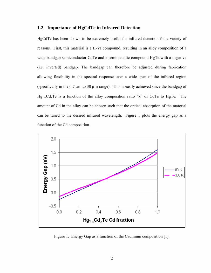
1.2 Importance of HgCdTe in Infrared Detection HgCdTe has been shown to be extremely useful for infrared detection for a variety of
reasons. First, this material is a II-VI compound, resulting in an alloy composition of a
wide bandgap semiconductor CdTe and a semimetallic compound HgTe with a negative
(i.e. inverted) bandgap. The bandgap can therefore be adjusted during fabrication
allowing flexibility in the spectral response over a wide span of the infrared region
(specifically in the 0.7 µm to 30 µm range). This is easily achieved since the bandgap of
Hg1-xCdxTe is a function of the alloy composition ratio “x” of CdTe to HgTe. The
amount of Cd in the alloy can be chosen such that the optical absorption of the material
can be tuned to the desired infrared wavelength. Figure 1 plots the energy gap as a
function of the Cd composition.
Figure 1. Energy Gap as a function of the Cadmium composition [1].
3
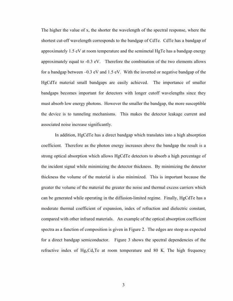
The higher the value of x, the shorter the wavelength of the spectral response, where the
shortest cut-off wavelength corresponds to the bandgap of CdTe. CdTe has a bandgap of
approximately 1.5 eV at room temperature and the semimetal HgTe has a bandgap energy
approximately equal to -0.3 eV. Therefore the combination of the two elements allows
for a bandgap between –0.3 eV and 1.5 eV. With the inverted or negative bandgap of the
HgCdTe material small bandgaps are easily achieved. The importance of smaller
bandgaps becomes important for detectors with longer cutoff wavelengths since they
must absorb low energy photons. However the smaller the bandgap, the more susceptible
the device is to tunneling mechanisms. This makes the detector leakage current and
associated noise increase significantly.
In addition, HgCdTe has a direct bandgap which translates into a high absorption
coefficient. Therefore as the photon energy increases above the bandgap the result is a
strong optical absorption which allows HgCdTe detectors to absorb a high percentage of
the incident signal while minimizing the detector thickness. By minimizing the detector
thickness the volume of the material is also minimized. This is important because the
greater the volume of the material the greater the noise and thermal excess carriers which
can be generated while operating in the diffusion-limited regime. Finally, HgCdTe has a
moderate thermal coefficient of expansion, index of refraction and dielectric constant,
compared with other infrared materials. An example of the optical absorption coefficient
spectra as a function of composition is given in Figure 2. The edges are steep as expected
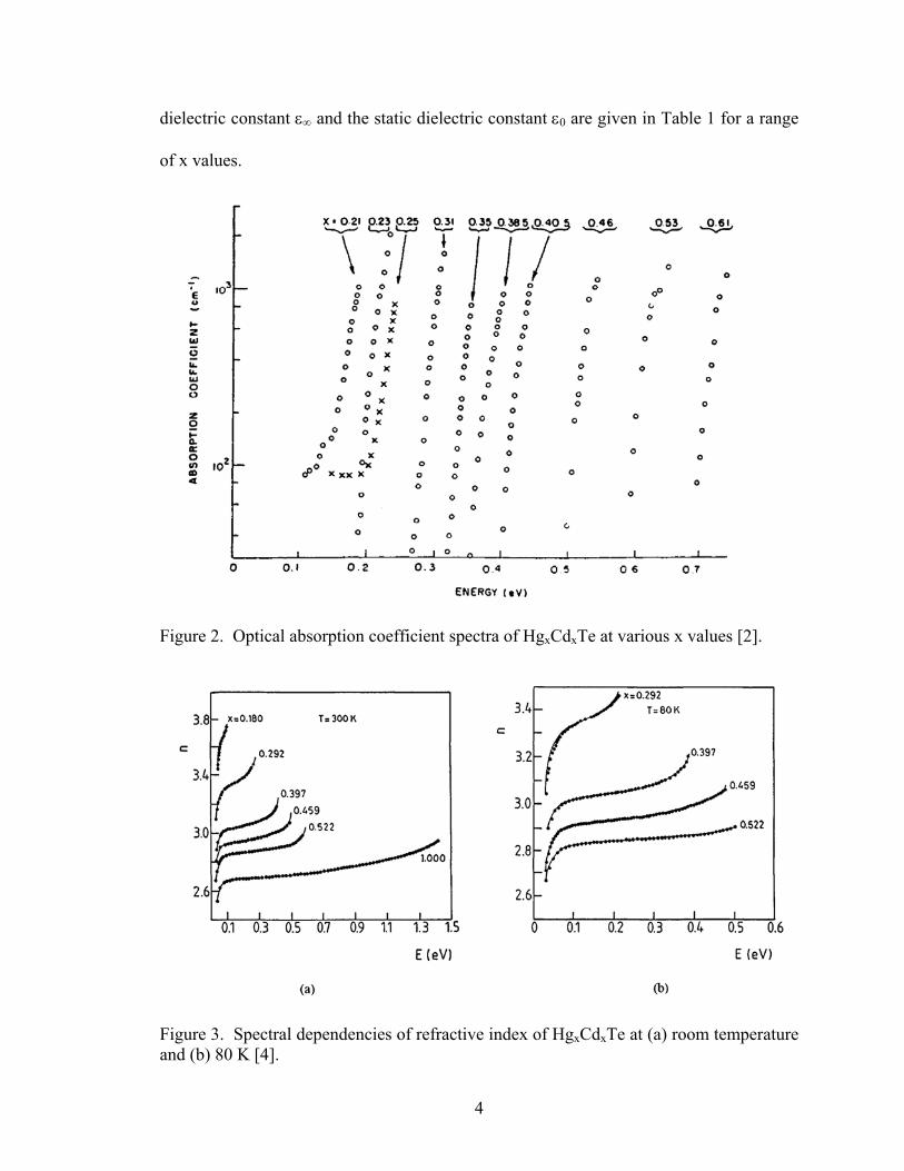
for a direct bandgap semiconductor. Figure 3 shows the spectral dependencies of the
refractive index of HgxCdxTe at room temperature and 80 K. The high frequency
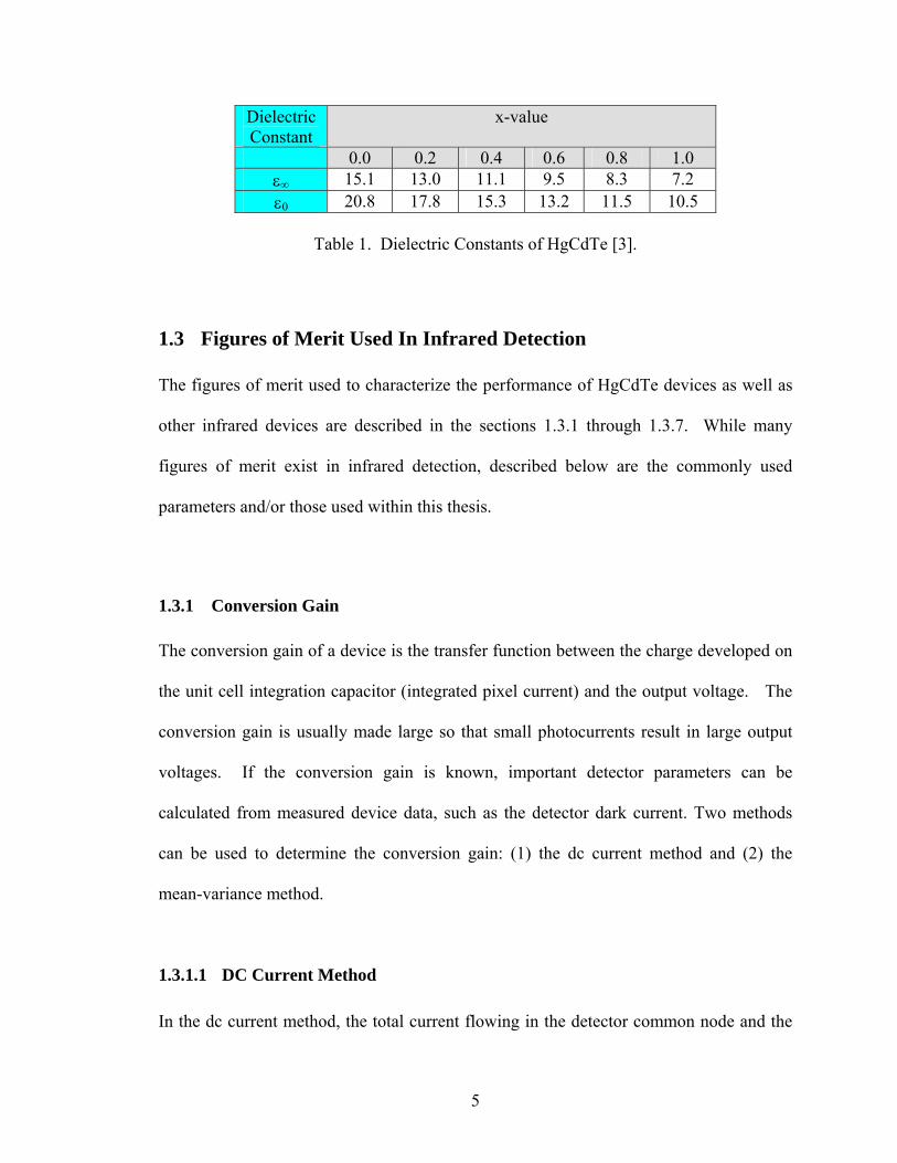
4
dielectric constant ε∞ and the static dielectric constant ε0 are given in Table 1 for a range
of x values.
Figure 2. Optical absorption coefficient spectra of HgxCdxTe at various x values [2].
Figure 3. Spectral dependencies of refractive index of HgxCdxTe at (a) room temperature and (b) 80 K [4].
5
Dielectric Constant
x-value
0.0 0.2 0.4 0.6 0.8 1.0 ε∞ 15.1 13.0 11.1 9.5 8.3 7.2 ε0 20.8 17.8 15.3 13.2 11.5 10.5
Table 1. Dielectric Constants of HgCdTe [3].
1.3 Figures of Merit Used In Infrared Detection The figures of merit used to characterize the performance of HgCdTe devices as well as
other infrared devices are described in the sections 1.3.1 through 1.3.7. While many
figures of merit exist in infrared detection, described below are the commonly used
parameters and/or those used within this thesis.
1.3.1 Conversion Gain The conversion gain of a device is the transfer function between the charge developed on
the unit cell integration capacitor (integrated pixel current) and the output voltage. The
conversion gain is usually made large so that small photocurrents result in large output
voltages. If the conversion gain is known, important detector parameters can be
calculated from measured device data, such as the detector dark current. Two methods
can be used to determine the conversion gain: (1) the dc current method and (2) the
mean-variance method.
1.3.1.1 DC Current Method
In the dc current method, the total current flowing in the detector common node and the
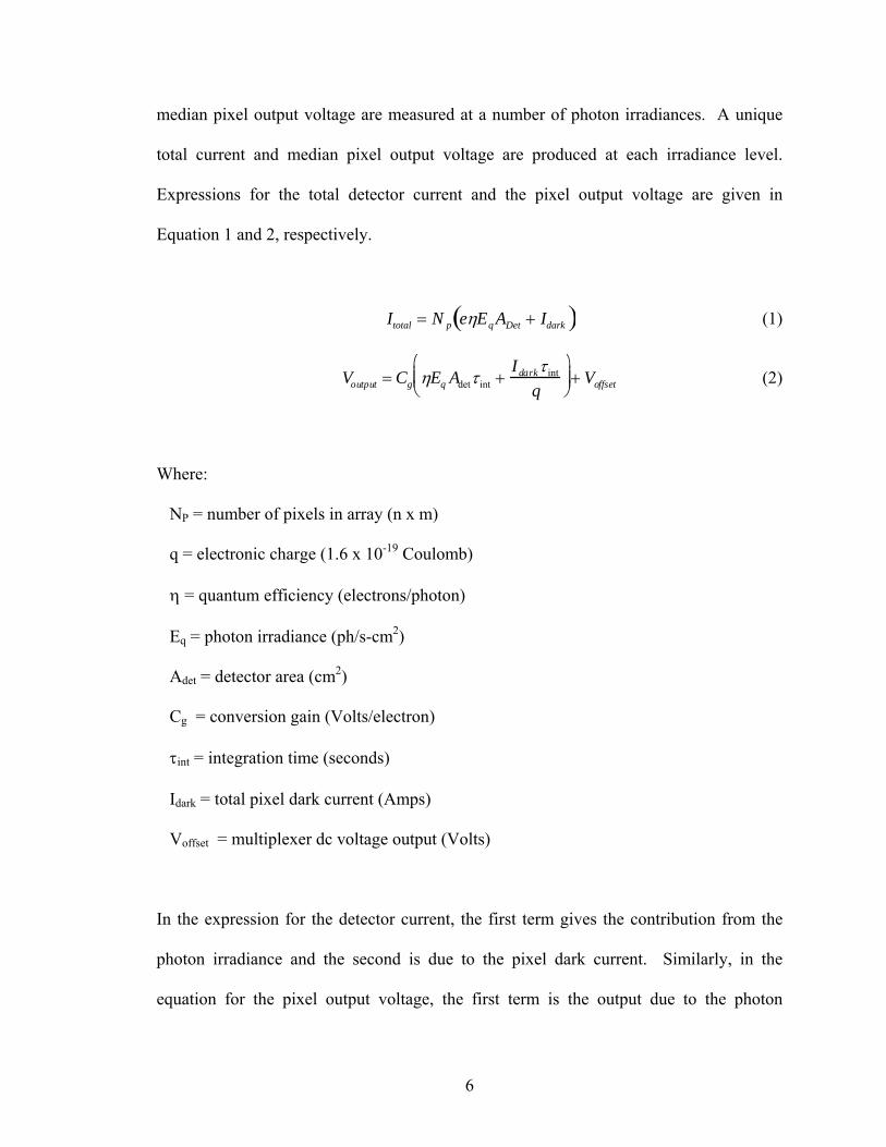
6
median pixel output voltage are measured at a number of photon irradiances. A unique
total current and median pixel output voltage are produced at each irradiance level.
Expressions for the total detector current and the pixel output voltage are given in
Equation 1 and 2, respectively.
Itotal = N p eηEq ADet + Idark( ) (1)
Voutput = Cg ηEq Adetτ int +
Idarkτ int
q
⎛
⎝ ⎜ ⎜
⎞
⎠ ⎟ ⎟ + Voffset (2)
Where:
NP = number of pixels in array (n x m)
q = electronic charge (1.6 x 10⁻¹⁹ Coulomb)
η = quantum efficiency (electrons/photon)
Eq = photon irradiance (ph/s-cm2)
Adet = detector area (cm2)
Cg = conversion gain (Volts/electron)
τint = integration time (seconds)
Idark = total pixel dark current (Amps)
Voffset = multiplexer dc voltage output (Volts)
In the expression for the detector current, the first term gives the contribution from the
photon irradiance and the second is due to the pixel dark current. Similarly, in the
equation for the pixel output voltage, the first term is the output due to the photon
7
irradiance, the second term is due to the pixel dark current, and the third is a constant due
to the multiplexer circuitry. An expression for the photon current in terms of the pixel
output voltage is given by:
Itotal =qNe
Cgτ int
⎛
⎝ ⎜ ⎞
⎠ ⎟ Voutput (3)
When the measured current is plotted as a function of the output voltage, a straight line is
usually obtained if the device does not have an excessive number of high dark current
pixels. The slope of this line is then used to determine the conversion gain using
Equation 4, which gives an average value for the entire array
dItotal
dVoutput
=qNe
Cgτ int
⎛
⎝ ⎜ ⎞
⎠ ⎟ =∆I∆V
=N p ∆i∆V
= N p
∆Qi
τ int
⎛ ⎝ ⎜
⎞ ⎠ ⎟
∆V= N p
q∆Ne
τ int
⎛ ⎝ ⎜
⎞ ⎠ ⎟
∆V
CgVolts
electron⎛ ⎝
⎞ ⎠ ≡
∆V∆Ne
=qN p
τ int •dItotal
dVoutput
⎛
⎝ ⎜ ⎞
⎠ ⎟
(4)
Where:
∆I = change in total detector current (Amps)
∆V = change in median output voltage (Volts)
∆i = average change in single pixel current (Amps)
Ne = number of electrons
∆Qi = change in charge integrated for one pixel (Coulombs)
8
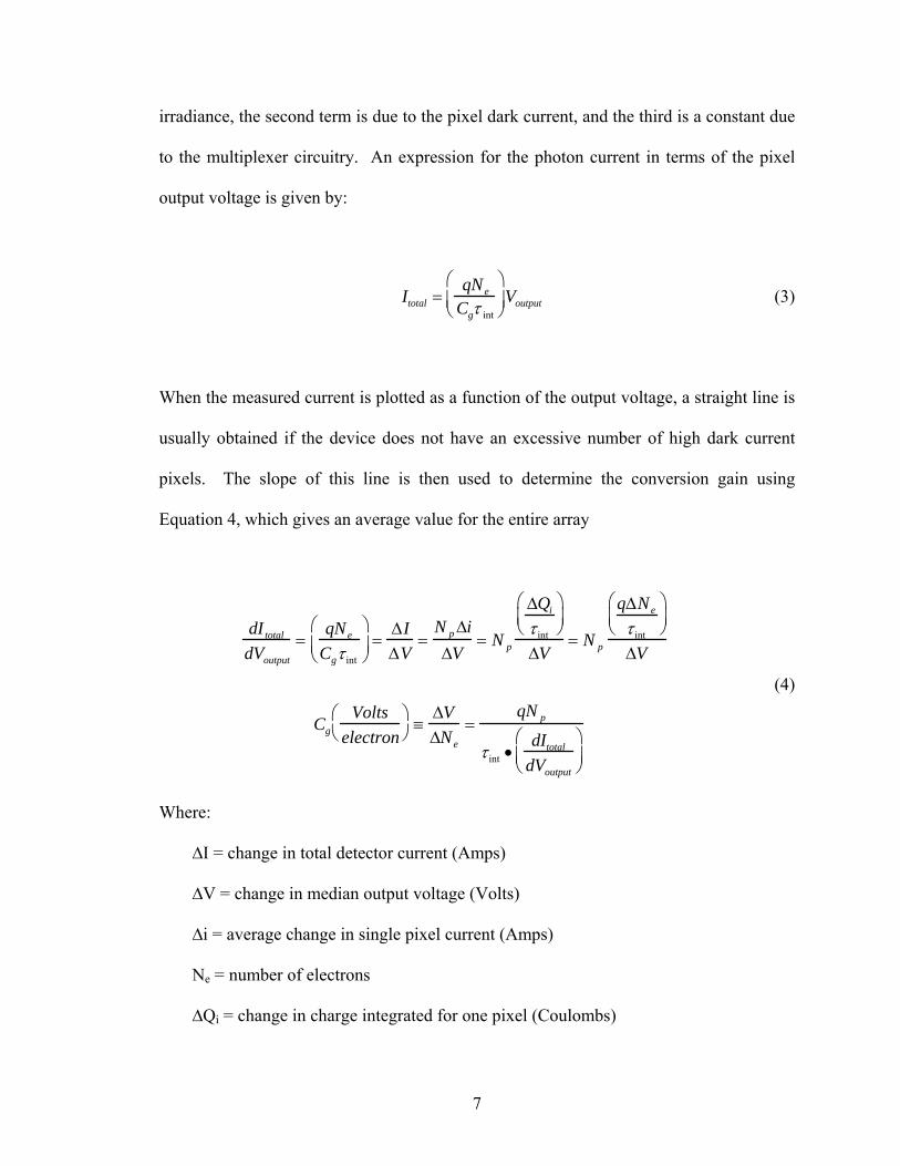
1.3.1.2 Mean Variance Method
If the pixel noise is dominated by photon noise, the mean-variance method can be used to
determine the conversion gain. Equation 5 gives an expression for photon noise from a
pixel. If this expression is squared and the expression for the quantity, ηEqAdetτint, is
substituted into the equation for pixel output voltage, we obtain Equation 6, the pixel
variance (square of noise) as a function of pixel output voltage. Thus, the conversion
gain is the slope of a plot of the variance versus the output voltage.
Noisephoton = Cg ηEq Adetτ int RMS Volts( ) (5)
NoisePhoton
2 = Cg •VOutput −Cg
Cg Idarkτ int
q
⎛
⎝ ⎜ ⎜
⎞
⎠ ⎟ ⎟ Volts( )2
(6)
To obtain the conversion gain data, pixel output voltages and RMS noises are measured
at a number of photon irradiances. The output level for each pixel is the average of the
output for a number of consecutive frames and the noise is the RMS deviation of the
output around its average value for the same number of frames. The variance is then
plotted as a function of the output voltage and the conversion gain is determined. This
process can be performed for individual pixels, but in practice, median outputs and noise
are typically used.
1.3.2 Responsivity The responsivity of the detector is defined as the ratio of the device output to an incident
stimulus and can be expressed in Volts or Amps. The stimulus is expressed in Watts or
9
photons/sec. The device output voltage should be a linear function of the stimulus, which
in our case is the incident photon irradiance, (within the linear range of the ROIC) as
given by Equation 2.
The responsivity is proportional to the slope of output versus photon irradiance as
expressed in Equation 7.
Responsivity = Cgη =dVOutput
d Eq Adetτ int( )=1
Adetτ int
dVOutput
d Eq( ) Volts
photon⎛ ⎝ ⎜ ⎞
⎠ (7)
To obtain the responsivity, the values for detector area and integration time are used with
Equation 7 and the measured slope of the output voltage versus photon irradiance. The
responsivity values are reported at the peak wavelength for the particular waveband being
measured. The responsivity data can be presented in various forms including array
medians versus irradiance, full array distributions, and ordered pixel plots. The detector
quantum efficiency (η), which is the ratio of output electrons to incident photons, can be
determined from the responsivity and the measured conversion gain as shown in Equation
7.
1.3.3 Dark Current Detector dark current is the current produced when no light is incident on the device. To
achieve this condition the detector should face a cold shield in the dewar. The device
performance is optimal when the dark current is low. The method of determining the
device dark current is described below.
To determine the dark current the expression for pixel output voltage (Equation 2)
with respect to integration time should be differentiated, which yields:
10
d VOutput( )d τ int( ) = Cgη Eq Adet +
Cg Idark
q
=Cg
qη qEq Adet( )+ Idark[ ]
(8)
The first term in the brackets is the pixel current due to the photon irradiance and the
second term is the pixel current due dark current. To obtain the dark current output
voltage measurements are made as a function of integration time at a very low photon
irradiance and these output data are plotted as a function of integration time. The dark
current can then be calculated from the slope of this plot and Equation 9, since all other
parameters in this Equation are known.
Idark Amps( )=
qCg
d VOutput( )d τ int( ) −ηqEq Adet (9)
1.3.4 Detectivity (D*) The specific detectivity, D*, is the detector parameter which normalizes the detector
sensitivity to a 1-cm2 detector area and a 1 Hz noise equivalent bandwidth. It is a
measure of the device signal-to-noise ratio (SNR), therefore, higher the D* the better the
sensitivity of the device. The specific detectivity is defined using Equation 10.
NEPfA
D id ∆=* (10)
11
Where ∆f is the noise equivalent bandwidth, in is the total device noise current and NEP
is the noise equivalent power. The total device current, in, includes all the different types
of noise such as thermal noise, photon noise, generation-recombination noise, 1/f noise,
readout noise, etc. The units of D* are defined as [Jones] which equals [ ]wattHzcm / .
1.3.5 Noise Equivalent Input (NEI) The Noise Equivalent Input, NEI, is a measure of the device sensitivity, based on the
pixel noise-to-signal ratio as expressed by:
NEIphotonssample
⎛ ⎝ ⎜ ⎞
⎠ =
RMS Noise (Volts)
Responsivity Voltsphoton
⎛ ⎝ ⎜ ⎞
⎠
(11)
This measure of sensitivity can also be computed as a Noise Equivalent Irradiance, where
the responsivity is expressed in units of [Volts/photon/sec-cm2]. NEIs can be presented
as array medians versus irradiance, full array NEI distributions, and full array sorted NEI
values. This measure of sensitivity is commonly used since it makes few assumptions.
1.3.6 Noise Equivalent Power (NEP) The Noise Equivalent Power, NEP, is defined as the minimum detectable power, i.e. the
number in Watts on the detector to produce a signal-to-noise ratio of unity. The NEP
depends on many parameters and comparison of detectors can only be made if other
device parameters are known such as the detector area, electrical bandwidth, spectral
region, detector bias and detector temperature. NEP can be specified for a value at a
12
specific wavelength (spectral NEP) or under broadband illumination (Blackbody NEP).
The smaller the NEP the better the device performance and it is generally used for
systems where the bandwidth is fixed.
RNEP noise
noisesignal
e ννν
φ== (12)
Where:
R = detector responsivity (Amperes/ Watt)
φe = radiant flux (Watts)
vsignal = detector signal (Amperes or Volts)
vnoise = detector noise (Amperes or Volts)
NEP is dominated by its dependence on the square root of the detector area and the
square root of the noise bandwidth. These two parameters must be specified with the
NEP to be used to compare device sensitivity.
1.3.7 Noise Equivalent Temperature Difference (NETD) The Noise Equivalent Temperature Difference, NETD, describes the performance of
thermal imaging systems. NETD is the temperature difference that produces a signal-to-
noise ratio of unity from the device. For the case where the detector D* is independent of
the optics F/# the NETD is described by:
( )
⎥⎥⎥⎥
⎦
⎤
⎢⎢⎢⎢
⎣
⎡
∂∂
∆=
dATLD
fFNETD
*
/#4 2
π (13)
13
Where:
F/# = f-number of optics
∆f = noise equivalent bandwidth
Ad = Detector Area
D* = Specific Detectivity
∂L ∂T = exitance contrast
Equation 13 gives the expression when the device is not Background Limited Infrared
Photodetector (BLIP). BLIP is defined as the condition when the background photon
flux is the dominant noise source and is much larger than the signal flux. For the case
where the detector is BLIP limited the NETD is described by:
( )
⎥⎥⎥⎥
⎦
⎤
⎢⎢⎢⎢
⎣
⎡
∂∂
∆=
ηλπd
q
ATL
LfFhcNETD/#22 (14)
Where:
Lq = photon flux sternace
η = detector quantum efficiency
λ = wavelength
h = Planck’s constant
c = speed of light
14
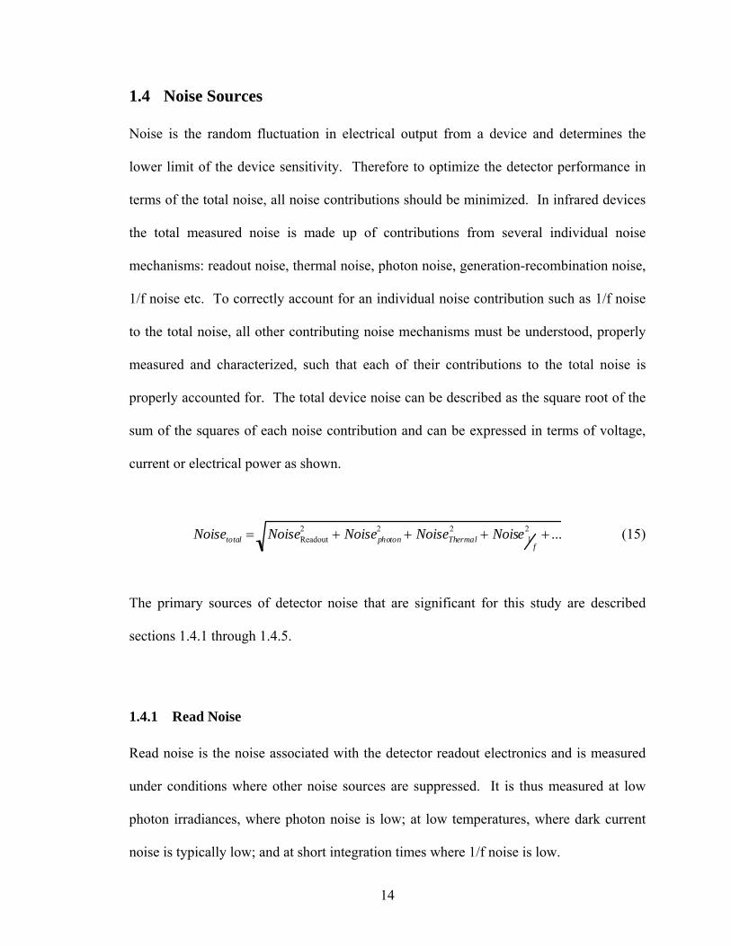
1.4 Noise Sources Noise is the random fluctuation in electrical output from a device and determines the
lower limit of the device sensitivity. Therefore to optimize the detector performance in
terms of the total noise, all noise contributions should be minimized. In infrared devices
the total measured noise is made up of contributions from several individual noise
mechanisms: readout noise, thermal noise, photon noise, generation-recombination noise,
1/f noise etc. To correctly account for an individual noise contribution such as 1/f noise
to the total noise, all other contributing noise mechanisms must be understood, properly
measured and characterized, such that each of their contributions to the total noise is
properly accounted for. The total device noise can be described as the square root of the
sum of the squares of each noise contribution and can be expressed in terms of voltage,
current or electrical power as shown.
Noisetotal = NoiseReadout
2 + Noisephoton2 + NoiseThermal
2 + Noise 1f
2 + ... (15)
The primary sources of detector noise that are significant for this study are described
sections 1.4.1 through 1.4.5.
1.4.1 Read Noise Read noise is the noise associated with the detector readout electronics and is measured
under conditions where other noise sources are suppressed. It is thus measured at low
photon irradiances, where photon noise is low; at low temperatures, where dark current
noise is typically low; and at short integration times where 1/f noise is low.
15
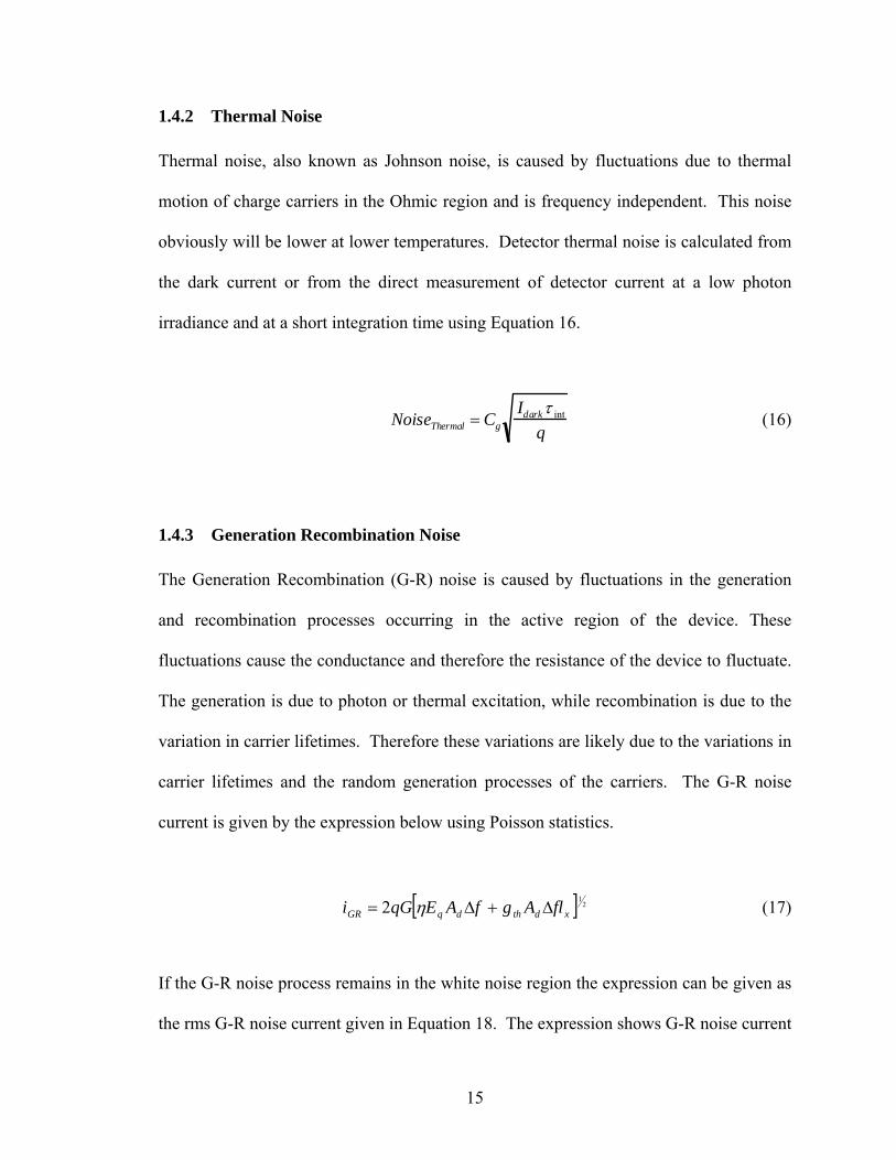
1.4.2 Thermal Noise Thermal noise, also known as Johnson noise, is caused by fluctuations due to thermal
motion of charge carriers in the Ohmic region and is frequency independent. This noise
obviously will be lower at lower temperatures. Detector thermal noise is calculated from
the dark current or from the direct measurement of detector current at a low photon
irradiance and at a short integration time using Equation 16.
NoiseThermal = Cg
Idarkτ int
q (16)
1.4.3 Generation Recombination Noise The Generation Recombination (G-R) noise is caused by fluctuations in the generation
and recombination processes occurring in the active region of the device. These
fluctuations cause the conductance and therefore the resistance of the device to fluctuate.
The generation is due to photon or thermal excitation, while recombination is due to the
variation in carrier lifetimes. Therefore these variations are likely due to the variations in
carrier lifetimes and the random generation processes of the carriers. The G-R noise
current is given by the expression below using Poisson statistics.
[ ] 21
2 xdthdqGR flAgfAEqGi ∆+∆= η (17)
If the G-R noise process remains in the white noise region the expression can be given as
the rms G-R noise current given in Equation 18. The expression shows G-R noise current
16
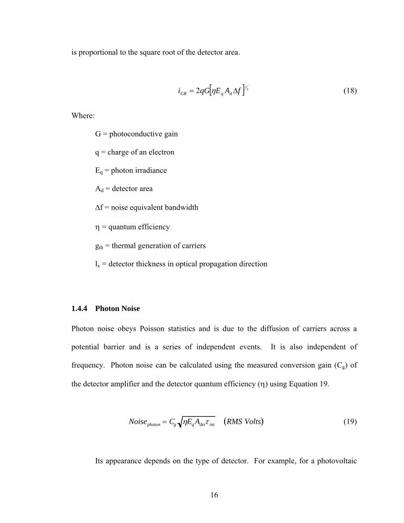
is proportional to the square root of the detector area.
[ ] 21
2 fAEqGi dqGR ∆= η (18)
Where:
G = photoconductive gain
q = charge of an electron
Eq = photon irradiance
Ad = detector area
∆f = noise equivalent bandwidth
η = quantum efficiency
gth = thermal generation of carriers
lx = detector thickness in optical propagation direction
1.4.4 Photon Noise Photon noise obeys Poisson statistics and is due to the diffusion of carriers across a
potential barrier and is a series of independent events. It is also independent of
frequency. Photon noise can be calculated using the measured conversion gain (Cg) of
the detector amplifier and the detector quantum efficiency (η) using Equation 19.
Noisephoton = Cg ηEq Adetτ int RMS Volts( ) (19)
Its appearance depends on the type of detector. For example, for a photovoltaic
17
detector it appears as shot noise while for a photoconductive detector it appears as
generation-recombination noise. Shot noise is associated with the current through the
potential barrier. If the detector noise is due to photons then it is background photon
noise limited or said to be BLIP limited.
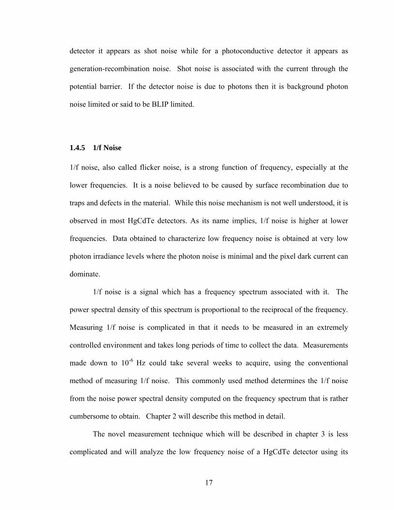
1.4.5 1/f Noise 1/f noise, also called flicker noise, is a strong function of frequency, especially at the
lower frequencies. It is a noise believed to be caused by surface recombination due to
traps and defects in the material. While this noise mechanism is not well understood, it is
observed in most HgCdTe detectors. As its name implies, 1/f noise is higher at lower
frequencies. Data obtained to characterize low frequency noise is obtained at very low
photon irradiance levels where the photon noise is minimal and the pixel dark current can
dominate.
1/f noise is a signal which has a frequency spectrum associated with it. The
power spectral density of this spectrum is proportional to the reciprocal of the frequency.
Measuring 1/f noise is complicated in that it needs to be measured in an extremely
controlled environment and takes long periods of time to collect the data. Measurements
made down to 10-6 Hz could take several weeks to acquire, using the conventional
method of measuring 1/f noise. This commonly used method determines the 1/f noise
from the noise power spectral density computed on the frequency spectrum that is rather
cumbersome to obtain. Chapter 2 will describe this method in detail.
The novel measurement technique which will be described in chapter 3 is less
complicated and will analyze the low frequency noise of a HgCdTe detector using its
18
empirical relationship to the detector dark current given by the equation [7]:
211
f
Ii dark
f
βα= (20)
Where:
i1/f = detector 1/f current noise (RMS Amps/Hz1/2)
α and β = empirical parameters, Typically β = 1
Idark = pixel park current (Amps)
f = frequency (Hz)
In a device, the output voltage at the end of each frame is due to the integration of
the pixel current on a capacitor for one integration time. In this integration process, the
output voltage includes noise from many frequencies. If the signal chain has a flat
frequency response over the frequency band of interest, the total 1/f noise current due to
all frequencies can be estimated using Equation 21.
I 1f ,total
=α Idark
f1
2
⎛
⎝ ⎜
⎞
⎠ ⎟
2
dff1
f2
∫⎡
⎣
⎢ ⎢
⎤
⎦
⎥ ⎥
12
(21)
Where:
f1 = 1/TR (Hz)
f2 = 1/(2τ) (Hz)
TR = re-calibration time or measurement time (seconds)
τ = integration time (seconds)
19
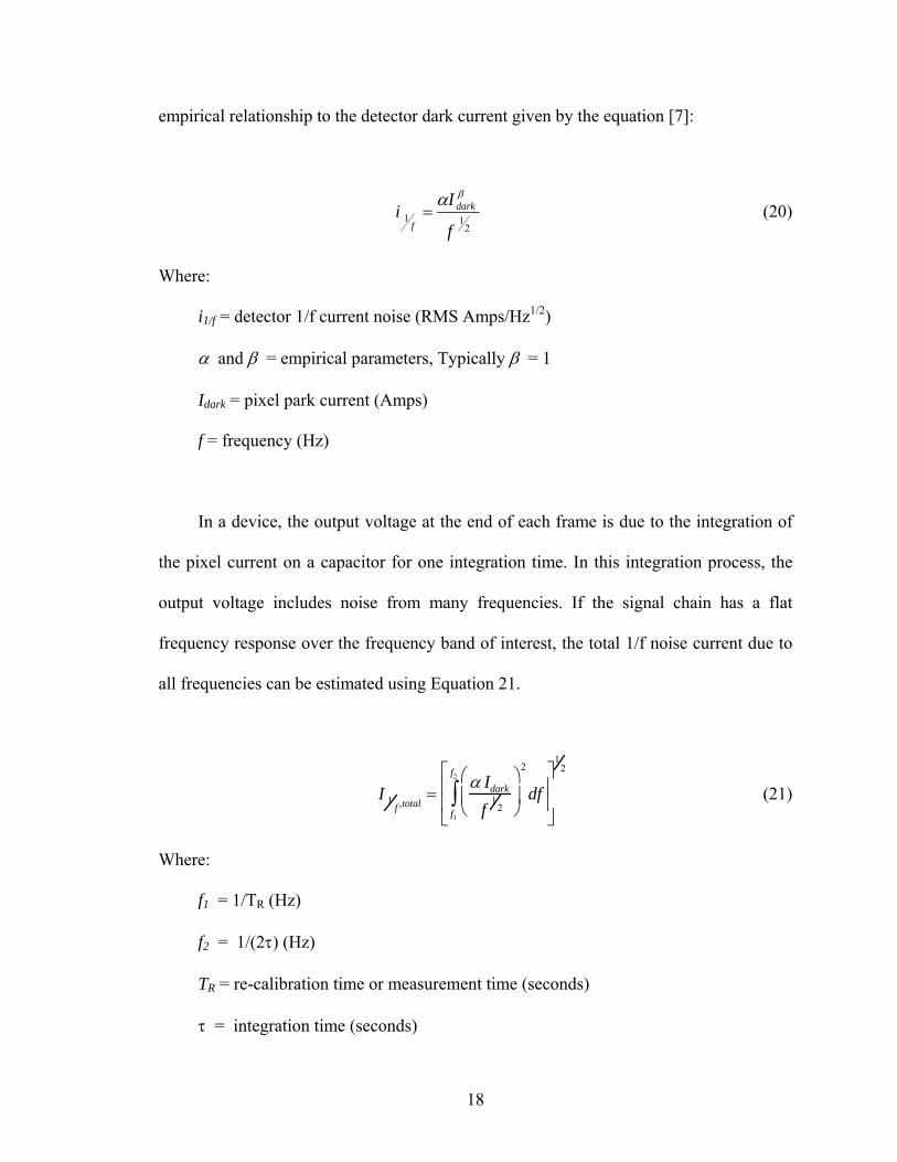
The re-calibration time is the time period over which data is taken to compute the noise
(standard deviation of the data). For the noise data presented in this thesis, one hundred
(100) frames of data were collected for each measurement, and the re-calibration time is
thus 100 times the device frame time. Equation 21 can be converted to noise voltage
using the device conversion gain and the integration time as given by Equation 22.
Noise1/ f =Cgτ intαIdark
q1
f 1/ 2
⎛ ⎝ ⎜
⎞ ⎠ ⎟
2
df1T R
12τ int
∫
=Cgτ intαIdark
qln
TR
2τ int
⎛ ⎝ ⎜
⎞ ⎠ ⎟
(22)
To properly account for the total 1/f noise the α-coefficient must be determined. In
chapter 3 the novel measurement technique will describe this process in detail. For
HgCdTe detectors, values of α and β depend on the cut-off wavelength of the detector,
the operating temperature, and the RoA (resistance-area product) of the detector. RoA is a
characteristic of the detector material and the process by which it was fabricated. The
detector sensitivity is proportional to the device RoA. The higher the RoA the higher the
output signal-to-noise ratio. For HgCdTe devices the RoA is low due to its inverse
proportionality to the square of the intrinsic-carrier concentration. This results in a
limited range for BLIP operation.
20
1.5 1/f Noise in HgCdTe Devices As with many semiconductor devices, HgCdTe detectors suffer from 1/f noise which can
limit their sensitivity[5,6]. It is therefore important to minimize the 1/f noise contribution
to the total noise such that BLIP can be achieved. Reducing the 1/f noise will improve
performance and allow operation of these devices at lower frequencies and longer
integration times. In addition, when these devices are integrated into a camera system a
calibration process must take place to suppress variations in the responsivity and dc offset
of the system caused by the 1/f noise drift characteristics. This calibration process
requires an accurate and uniform calibration source and often these systems have to
continuously be re-calibrated. Therefore it is emphasized again, that it is significant to
accurately account for the 1/f noise and minimize its contribution if possible.
The origin of 1/f noise in HgCdTe devices is not well understood. Many studies
have applied several theoretical approaches and have empirically correlated 1/f noise in
these devices with surface and dark currents [7-9]. Tobin has studied 1/f noise in
HgCdTe devices, where the study concluded that the 1/f noise was independent of
photocurrent and diffusion current and linearly dependent on surface leakage current.
Van der Ziel and Kleinpenning models which relate 1/f noise to the detector current,
show that the noise current is proportional to the square root of the dark current.
Kleinpenning’s model also predicts that the noise current should be proportional to the
square root of the detector area, since the device dark current is proportional to the area
for larger devices. Specifically these models have resulted in individual theories as to
which current mechanism contributes to the 1/f noise. For example, some researchers
attribute 1/f noise to diffusion [10-11], depletion region generation-recombination noise
21
[7][12], and tunneling [12-13]. Other models attribute 1/f noise to surface recombination
velocity[14] which is modulated by a fluctuation in the surface potential (caused by
tunneling from surface traps). Whatever the mechanism is, the 1/f noise in the device
results in a time-varying drift.
It is convenient to characterize the magnitude of 1/f noise in HgCdTe devices by
the α-coefficient. This parameter as defined by Hooge is the ratio of noise current in
units of bandwidth to the dark current. Hooge found that the current spectral density of
1/f noise of the fluctuating current is proportional to the square of the mean current value
and inversely proportional to the number of charge carries. The proportionality factor is
known as the Hooge coefficient, αH. The Hooge coefficient unified the noise process in
semiconductors with its inverse dependence on the number of charge carriers. Hooge
concluded that whatever electrons do when producing 1/f noise they do it independently.
Thus α is a normalized measure for the relative noise in different materials, under
different operating temperatures, bias voltage, etc. It was also determined that α
depends on the quality of the crystal and on the scattering mechanism that determines
mobility[15].
The study within this thesis is based on the model developed by Tobin, where the
novel 1/f noise measurement technique attributes the 1/f noise to surface generation
current and uses the linear relationship between the dark current and 1/f noise for its
development. To verify the accuracy of the novel measurement technique the voltage
noise spectra are measured as a function of time and converted to frequency using the
conventional method of measuring 1/f noise, at several temperatures and several reverse
biases. The power spectral densities are computed on the data and each noise current
22
power spectral density curve was fit in the relevant frequency range to determine the
empirical parameter α at each temperature for each bias. The α-coefficients extracted
from the noise current power spectral density data are compared with those determined
using the novel measurement technique to show the correlation between the two
measurement techniques. The next two chapters give detailed descriptions of the two 1/f
noise measurement techniques and discusses the experimental results.
23
Chapter 2
Measurement of 1/f Noise Using The Conventional Method
2.1 Measurement Conditions All measurements were performed at the Infrared Radiation Effects Laboratory, Air
Force Research Laboratory, Kirtland AFB, Albuquerque, NM. Measurements were made
with the device mounted in a liquid helium pour-filled cryogenic dewar. This
configuration allowed for low temperature studies, down to 40 K. The detector was wire
bonded to a leadless chip carrier (LCC) which was in intimate contact with the cold
finger. The temperature was continuously controlled at each operating temperature by a
Lakeshore Cryotronics model 330 temperature controller. A field-of-view limiting
aperture and a spectral band-pass filter, both mounted on a liquid helium cold shield, set
the background photon irradiance on the device. An external blackbody was used as the
source of signal irradiance and the spectral band-pass filter limited the spectral content of
the blackbody irradiances. For the geometry used, the fields-of-view of all pixels are
filled by the blackbody.
The DC voltage sources, dc current sources and ac clocks were provided to the
device through the test system which uses direct memory access (DMA) interfaced to a
computer where control of all system variables (system gain, offset, applied voltages and
currents, etc.) is made capable. Therefore all measurements were automated. The
timing routine, which generates the clock waveforms, for the device is created by a
24
software program, uploaded on a Programmable Logic Device (PLD) and then stored on
RAM. The RAM memory is cycled at the frequency determined by the device clocks.
The test system provides amplification, sampling and A/D conversion of the device
output. The output data is recorded to the computer where it can then be accessed and
analyzed.
Prior to measuring and characterizing the total noise at each temperature the device
was radiometrically characterized such that all critical parameters needed to correctly
model all noise sources could be determined. These parameters include optimal detector
bias, responsivity, quantum efficiency, conversion gain and dark current. Determination
of these parameters is critical in determining the 1/f noise contribution to the total
measured noise using both the conventional and novel 1/f noise measurement techniques.
2.1.1 Background Photon Irradiance The background irradiance due to 295 K room temperature radiation is calculated from a
product of the pixel field-of-view and a numerical integral of the product of the detector
spectral response, the spectral distribution of the photon exitance from a 295 K
blackbody, the transmittance of the cold neutral density filter and the transmittance of the
room temperature KRS-5 vacuum window as given by Equation 23.
Eq 295K( )= Ω M p λ,295K( )RRPH λ( )τ filter λ( )τWindow λ( )dλ
0
∞
∫ (23)
Where:
Eq(295K) = photon irradiance (295 K), ph/s-cm2
25
Ω = solid angle of the detector field-of-view, steradians
Mp(λ, 295K) = Blackbody photon exitance at 295 Kelvin, ph/s-cm2/steradian/µ
RRPH(λ) = detector relative spectral Response
τfilter (λ) = filter transmittance
τWindow(λ) = vacuum window transmittance
2.1.2 Signal Photon Irradiance Signal photon irradiances were similarly calculated using a numerical integral of the
product of the detector spectral response, the pixel field-of-view, the spectral distribution
of the photon exitance from the blackbody, and the spectral transmittances of the spectral
filter, the cold neutral density filter, and the vacuum window as given by Equation 24.
The irradiances for the device are calculated relative to its spectral response curve
normalized to the center of the spectral filter. By using various blackbody temperatures,
a wide range of photon irradiances was available for these measurements.
Eq T( )= Ω M p λ,T( )RRPH λ( )τ filter λ( )τWindow λ( )dλ
0
∞
∫ (24)
Where:
Eq(T) = signal photon irradiance from a blackbody at temperature, T, ph/s-cm2
Mp(λ,T) = Blackbody photon exitance evaluated at temperature, T,
ph/s-cm2/steradians/µ
26
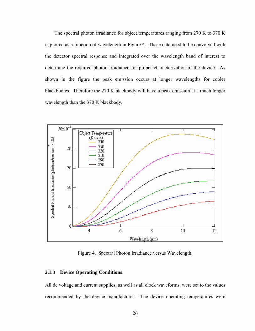
The spectral photon irradiance for object temperatures ranging from 270 K to 370 K
is plotted as a function of wavelength in Figure 4. These data need to be convolved with
the detector spectral response and integrated over the wavelength band of interest to
determine the required photon irradiance for proper characterization of the device. As
shown in the figure the peak emission occurs at longer wavelengths for cooler
blackbodies. Therefore the 270 K blackbody will have a peak emission at a much longer
wavelength than the 370 K blackbody.
Figure 4. Spectral Photon Irradiance versus Wavelength.
2.1.3 Device Operating Conditions All dc voltage and current supplies, as well as all clock waveforms, were set to the values
recommended by the device manufacturer. The device operating temperatures were
27
obtained by heating and controlling the temperature of the device mount within the test
dewar.
2.2 Radiometric Characterization
Radiometric performance data were obtained on the device to determine essential
parameters which were used to correctly account for the 1/f noise contribution. Several
operational parameters that were varied during these data collections include temperature,
integration time, detector bias, and photon irradiance. Results are reported for pixels
representing the median values as well as pixels representing data in the tails of the data
distributions, i.e. pixels in the 90th and 95th percentiles. In the remainder of this section,
the data analysis used to quantify the device performance is described. The figures of
merit which where used have been previously described in chapter 1.
2.2.1 DC Currents, Voltages, and Power Dissipation
The voltages applied and the currents obtained from each device node are important
measures of the health of the device and provide a measure of its power dissipation.
These monitored voltage and current values verified the device was operating correctly
before critical measurements began. In addition, by monitoring these device values
throughout the experiment it was verified the device operation had not changed for the
entire duration of the experiment.
28
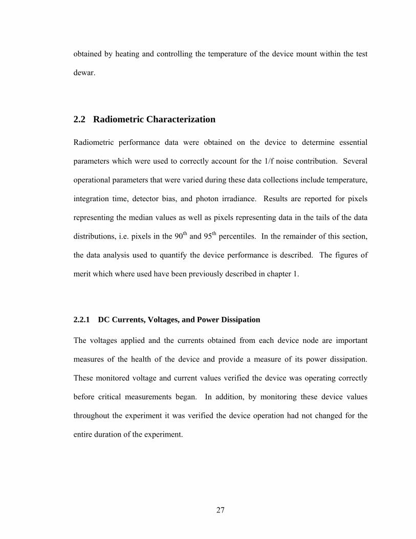
2.2.2 Bias Optimization
Prior to radiometrically characterizing the device, the optimal detector bias was
determined. The output and noise data as a function of bias were collected at two photon
irradiance levels, a high level of 4.7 x 10¹² ph/sec-cm2 and a low value of 1.1 x 10¹²
ph/sec-cm2. From the data the responsivity and NEI are calculated for each detector bias,
which was varied by externally changing the bias node voltage. Figure 5 plots the
median device pixel outputs as a function of the applied bias at the higher irradiance and
Figure 6 is the output at the lower irradiance. This data show that the reverse I/V
characteristics are dependant on bias at each operating temperature.
Figure 5. Pixel Output versus Applied Bias at 4.7 x 10¹² ph/sec-cm2.
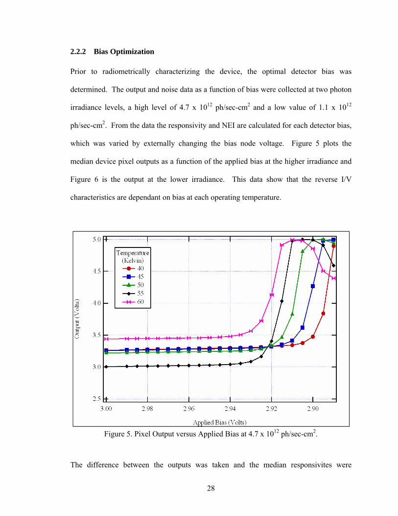
The difference between the outputs was taken and the median responsivites were
29
calculated using the calculated irradiance values and given integration time and detector
area. The integration time for the data taken at 60 K needed to be shortened in
comparison to the other temperatures due to the output saturating at the longer integration
time where all other measurements were taken. This is shown in Figure 5 where the
voltage output level is greater than all the other output voltage levels measured for the
lower temperatures. The median NEI was determined at the lower irradiance using the
measured noise and calculated responsivities of each pixel. The median responsivity and
median NEI values as function of the applied bias are shown in Figure 7 and Figure 8
respectively.
Figure 6. Pixel Output versus Applied Bias at 1.1 x 10¹² ph/sec-cm2.
30
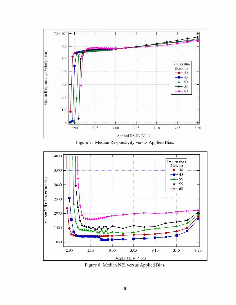
Figure 7. Median Responsivity versus Applied Bias.
Figure 8. Median NEI versus Applied Bias.
31
The responsivity operability was determined by the uniformity of the responsivity
distribution, were the operability is defined as the percentage of all pixels, which are not
classified as deviant pixels. An operable pixel is defined as a pixel that has a responsivity
within 25% of the median responsivity. The NEI operability was determined by the
uniformity of the NEI distribution, where the operability is defined as the percentage of
all pixels, which are again not classified as deviant pixels. An operable pixel is defined
as a pixel that has a NEI within a factor of two of the median device NEI. The detector
bias that provides the highest device responsivity operability as well as NEI operability is
selected as the optimal detector bias and is the detector bias at which all subsequent
measurements are performed. This optimization process was repeated at each
temperature, to account for shifts that occur in the detector bias with increasing or
decreasing temperature.
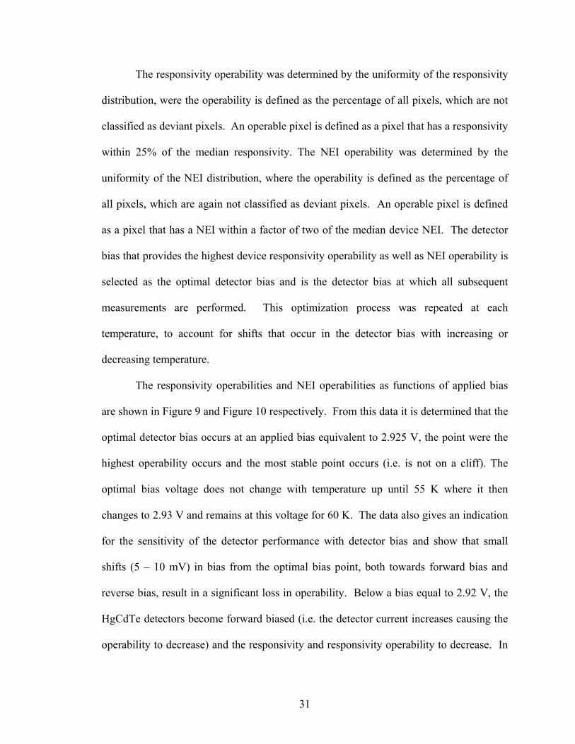
The responsivity operabilities and NEI operabilities as functions of applied bias
are shown in Figure 9 and Figure 10 respectively. From this data it is determined that the
optimal detector bias occurs at an applied bias equivalent to 2.925 V, the point were the
highest operability occurs and the most stable point occurs (i.e. is not on a cliff). The
optimal bias voltage does not change with temperature up until 55 K where it then
changes to 2.93 V and remains at this voltage for 60 K. The data also gives an indication
for the sensitivity of the detector performance with detector bias and show that small
shifts (5 – 10 mV) in bias from the optimal bias point, both towards forward bias and
reverse bias, result in a significant loss in operability. Below a bias equal to 2.92 V, the
HgCdTe detectors become forward biased (i.e. the detector current increases causing the
operability to decrease) and the responsivity and responsivity operability to decrease. In
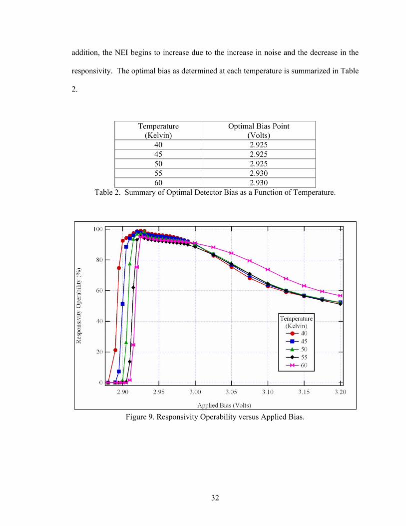
32
addition, the NEI begins to increase due to the increase in noise and the decrease in the
responsivity. The optimal bias as determined at each temperature is summarized in Table
2.
Temperature (Kelvin)
Optimal Bias Point (Volts)
40 2.925 45 2.925 50 2.925 55 2.930 60 2.930
Table 2. Summary of Optimal Detector Bias as a Function of Temperature.
Figure 9. Responsivity Operability versus Applied Bias.
33
Figure 10. NEI Operability versus Applied Bias.
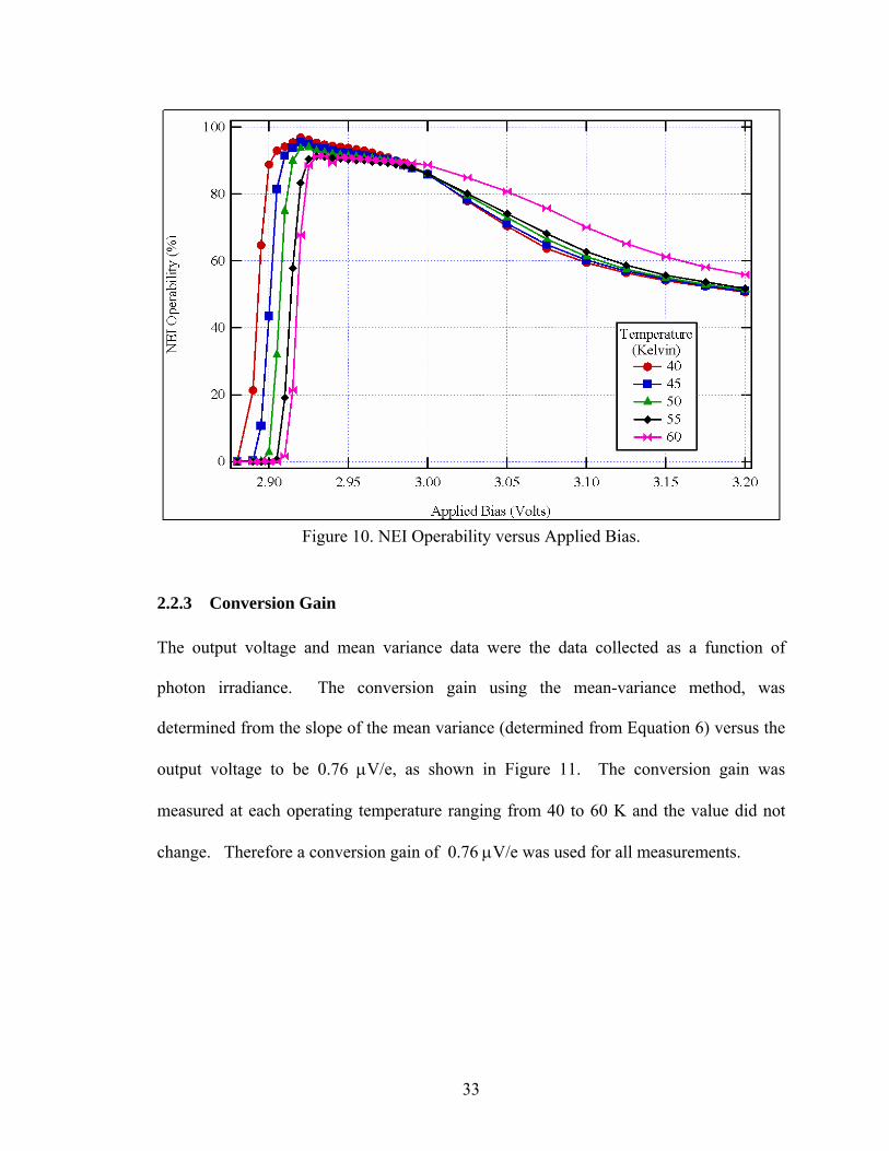
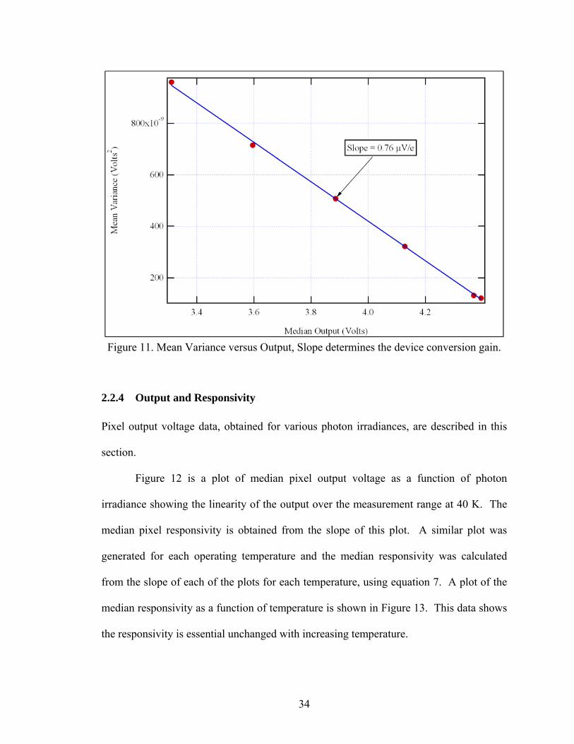
2.2.3 Conversion Gain The output voltage and mean variance data were the data collected as a function of
photon irradiance. The conversion gain using the mean-variance method, was
determined from the slope of the mean variance (determined from Equation 6) versus the
output voltage to be 0.76 µV/e, as shown in Figure 11. The conversion gain was
measured at each operating temperature ranging from 40 to 60 K and the value did not
change. Therefore a conversion gain of 0.76 µV/e was used for all measurements.
34
Figure 11. Mean Variance versus Output, Slope determines the device conversion gain.
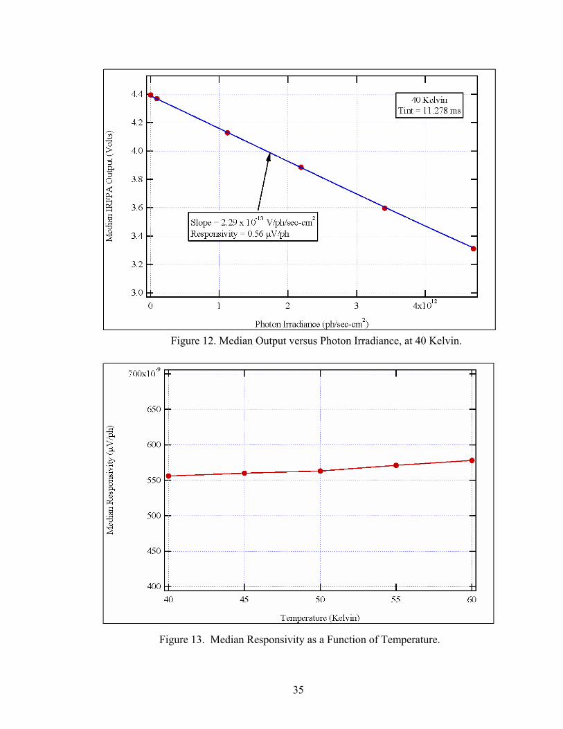
2.2.4 Output and Responsivity Pixel output voltage data, obtained for various photon irradiances, are described in this
section.
Figure 12 is a plot of median pixel output voltage as a function of photon
irradiance showing the linearity of the output over the measurement range at 40 K. The
median pixel responsivity is obtained from the slope of this plot. A similar plot was
generated for each operating temperature and the median responsivity was calculated
from the slope of each of the plots for each temperature, using equation 7. A plot of the
median responsivity as a function of temperature is shown in Figure 13. This data shows
the responsivity is essential unchanged with increasing temperature.
35
Figure 12. Median Output versus Photon Irradiance, at 40 Kelvin.
Figure 13. Median Responsivity as a Function of Temperature.
36
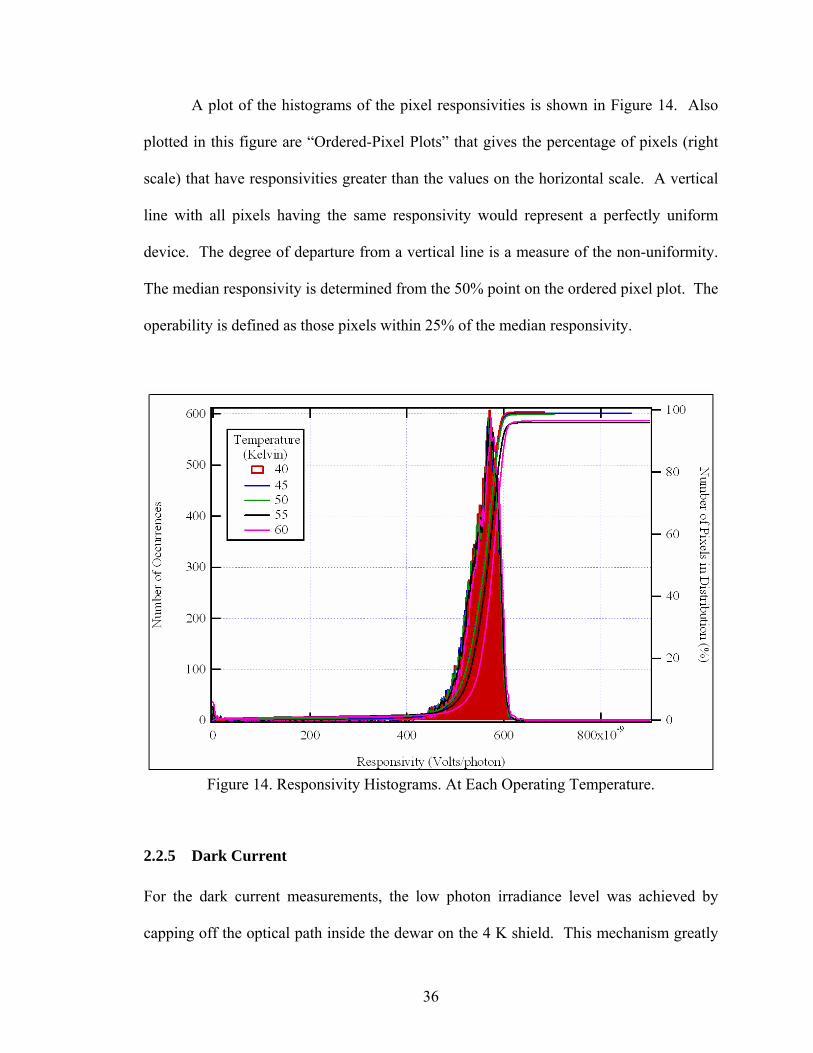
A plot of the histograms of the pixel responsivities is shown in Figure 14. Also
plotted in this figure are “Ordered-Pixel Plots” that gives the percentage of pixels (right
scale) that have responsivities greater than the values on the horizontal scale. A vertical
line with all pixels having the same responsivity would represent a perfectly uniform
device. The degree of departure from a vertical line is a measure of the non-uniformity.
The median responsivity is determined from the 50% point on the ordered pixel plot. The
operability is defined as those pixels within 25% of the median responsivity.
Figure 14. Responsivity Histograms. At Each Operating Temperature.
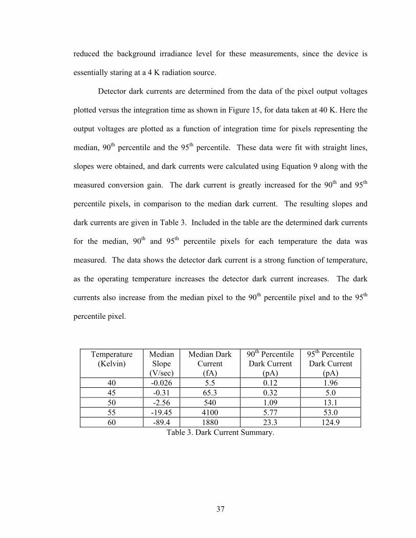
2.2.5 Dark Current For the dark current measurements, the low photon irradiance level was achieved by
capping off the optical path inside the dewar on the 4 K shield. This mechanism greatly
37
reduced the background irradiance level for these measurements, since the device is
essentially staring at a 4 K radiation source.
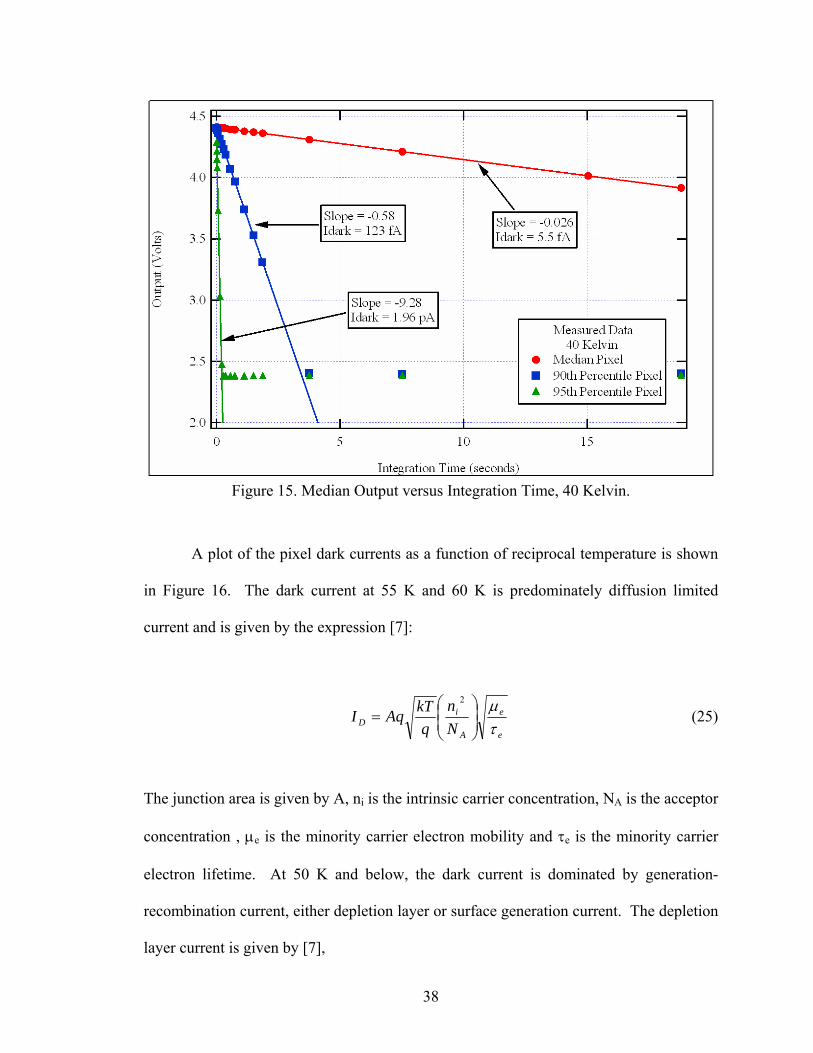
Detector dark currents are determined from the data of the pixel output voltages
plotted versus the integration time as shown in Figure 15, for data taken at 40 K. Here the
output voltages are plotted as a function of integration time for pixels representing the
median, 90th percentile and the 95th percentile. These data were fit with straight lines,
slopes were obtained, and dark currents were calculated using Equation 9 along with the
measured conversion gain. The dark current is greatly increased for the 90th and 95th
percentile pixels, in comparison to the median dark current. The resulting slopes and
dark currents are given in Table 3. Included in the table are the determined dark currents
for the median, 90th and 95th percentile pixels for each temperature the data was
measured. The data shows the detector dark current is a strong function of temperature,
as the operating temperature increases the detector dark current increases. The dark
currents also increase from the median pixel to the 90th percentile pixel and to the 95th
percentile pixel.
Temperature (Kelvin)
MedianSlope
(V/sec)
Median Dark Current
(fA)
90th Percentile Dark Current
(pA)
95th Percentile Dark Current
(pA) 40 -0.026 5.5 0.12 1.96 45 -0.31 65.3 0.32 5.0 50 -2.56 540 1.09 13.1 55 -19.45 4100 5.77 53.0 60 -89.4 1880 23.3 124.9
Table 3. Dark Current Summary.
38
Figure 15. Median Output versus Integration Time, 40 Kelvin.
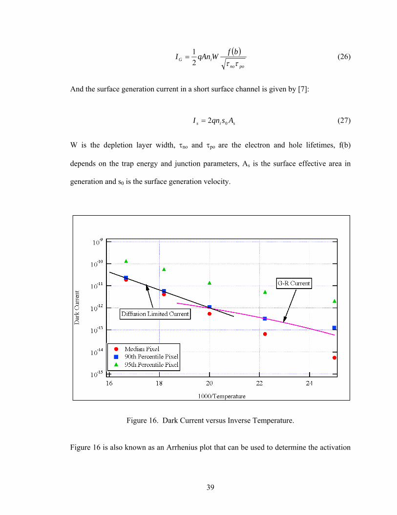
A plot of the pixel dark currents as a function of reciprocal temperature is shown
in Figure 16. The dark current at 55 K and 60 K is predominately diffusion limited
current and is given by the expression [7]:
e
e
A
iD N
nq
kTAqIτµ
⎟⎟⎠
⎞⎜⎜⎝
⎛=
2
(25)
The junction area is given by A, ni is the intrinsic carrier concentration, NA is the acceptor
concentration , µe is the minority carrier electron mobility and τe is the minority carrier
electron lifetime. At 50 K and below, the dark current is dominated by generation-
recombination current, either depletion layer or surface generation current. The depletion
layer current is given by [7],
39
( )pono
iGbfWqAnIττ2
1= (26)
And the surface generation current in a short surface channel is given by [7]:
sis AsqnI 02= (27)
W is the depletion layer width, τno and τpo are the electron and hole lifetimes, f(b)
depends on the trap energy and junction parameters, As is the surface effective area in
generation and s0 is the surface generation velocity.
Figure 16. Dark Current versus Inverse Temperature.
Figure 16 is also known as an Arrhenius plot that can be used to determine the activation
40
energy (Ea) of the device and therefore the device cutoff wavelength. It can be shown
that the log of the dark current is proportional to the activation energy by the expression
⎟⎠⎞
⎜⎝⎛−∝
TEI a
dark exp (28)
The activation energy determined from the slope of the Arrhenius plot and the above
expression verifies the dark currents determined as a function of temperature are correct
for a device of a particular cutoff wavelength. It therefore, also verifies that any trends
seen by the individual current mechanism (i.e diffusion, g-r, or surface currents) are also
being modeled correctly. An example would be, if the activation energy determined from
the Arrhenius plot is 0.5 eV for a material with a bandgap energy of 1.24 eV, then the
resulting cutoff wavelength would correspond to approximately 2.5 microns. This cutoff
wavelength should be the cutoff wavelength of the device under test.
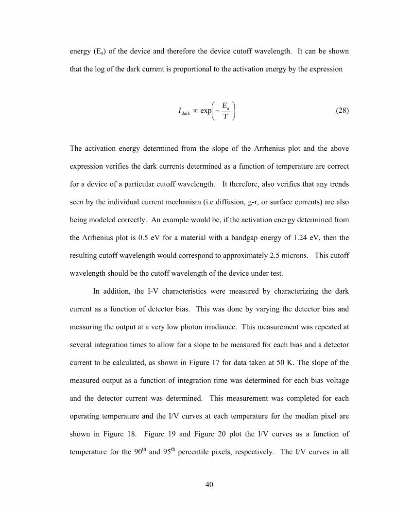
In addition, the I-V characteristics were measured by characterizing the dark
current as a function of detector bias. This was done by varying the detector bias and
measuring the output at a very low photon irradiance. This measurement was repeated at
several integration times to allow for a slope to be measured for each bias and a detector
current to be calculated, as shown in Figure 17 for data taken at 50 K. The slope of the
measured output as a function of integration time was determined for each bias voltage
and the detector current was determined. This measurement was completed for each
operating temperature and the I/V curves at each temperature for the median pixel are
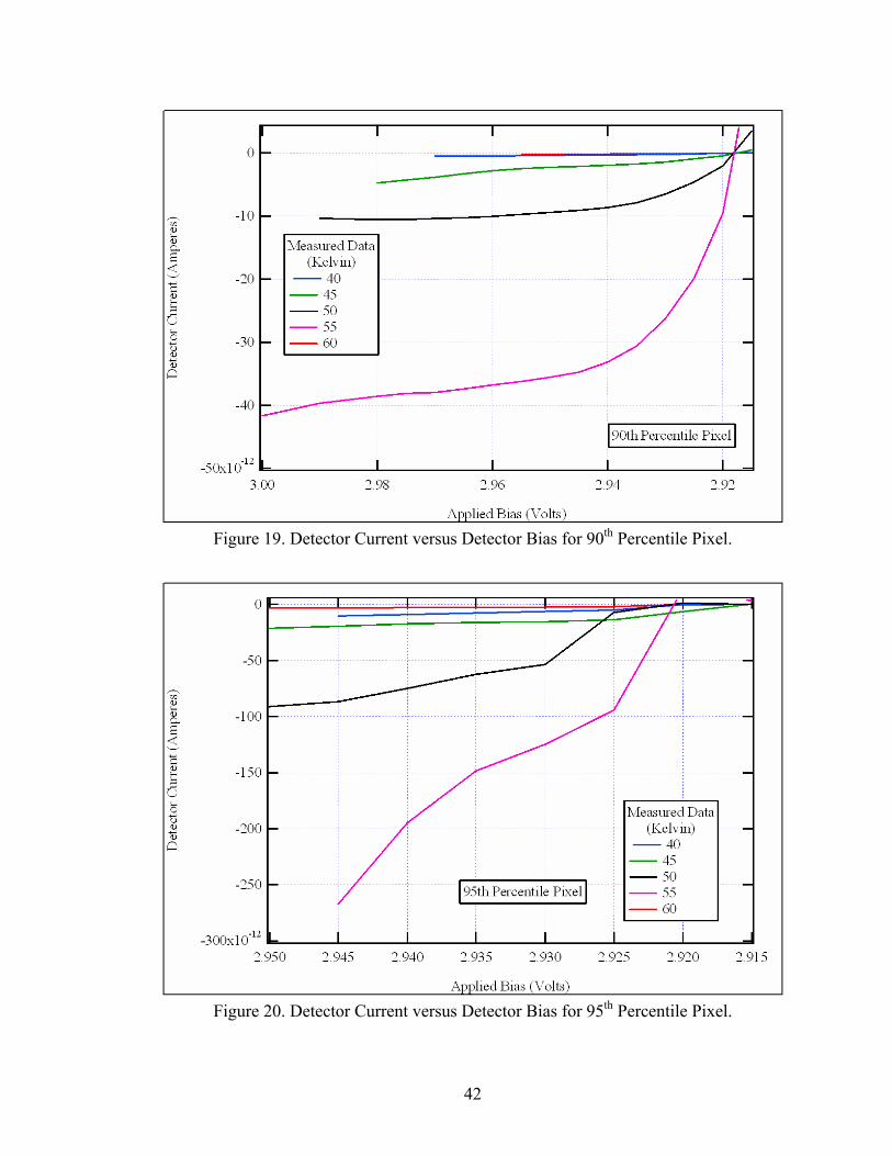
shown in Figure 18. Figure 19 and Figure 20 plot the I/V curves as a function of
temperature for the 90th and 95th percentile pixels, respectively. The I/V curves in all
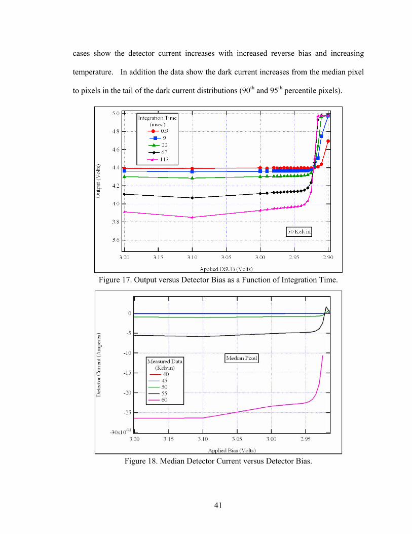
41
cases show the detector current increases with increased reverse bias and increasing
temperature. In addition the data show the dark current increases from the median pixel
to pixels in the tail of the dark current distributions (90th and 95th percentile pixels).
Figure 17. Output versus Detector Bias as a Function of Integration Time.
Figure 18. Median Detector Current versus Detector Bias.
42
Figure 19. Detector Current versus Detector Bias for 90th Percentile Pixel.
Figure 20. Detector Current versus Detector Bias for 95th Percentile Pixel.
43
2.2.6 Noise Pixel noise data obtained at various combinations of integration time and photon
irradiance are presented in this section. Although the data presented within this section
shows the 1/f noise contribution to the total noise; the details as it pertains to the novel
measurement technique developed for measuring 1/f noise will be discussed in detail in
the next chapter.
Pixel noise is calculated as the RMS deviation of the pixel output voltage about its
average for a set number of consecutive frames of data. The measured noise always
includes contributions from both readout and detector; detector noise includes
contributions from photon noise, thermal noise, and 1/f noise. By modeling each of these
noise sources the total device noise can also be modeled and compared to the total
measured noise. From the measured data it is possible to determine which is the most
significant for different combinations of operating temperature, integration time, and
photon irradiance. To recall, from chapter 1 the total device noise is determined from the
individual contributions of each noise source. Therefore the total device noise can be
described as the square root of the sum of the squares of: (1) readout noise; (2) photon
noise; (3) dark current shot noise; and (4) 1/f noise given by Equation 15. The equations
and methods of determining each of these noise contributions was described in chapter 1
section 4.
The median pixel noise as a function of photon irradiance at 40 K is shown in
Figure 21. At the nominal operating integration time, the dominant noises are readout
noise at lower irradiances and photon noise at higher irradiances. Under these operating
conditions, detector thermal and 1/f noise contribute minimally to the total noise for the
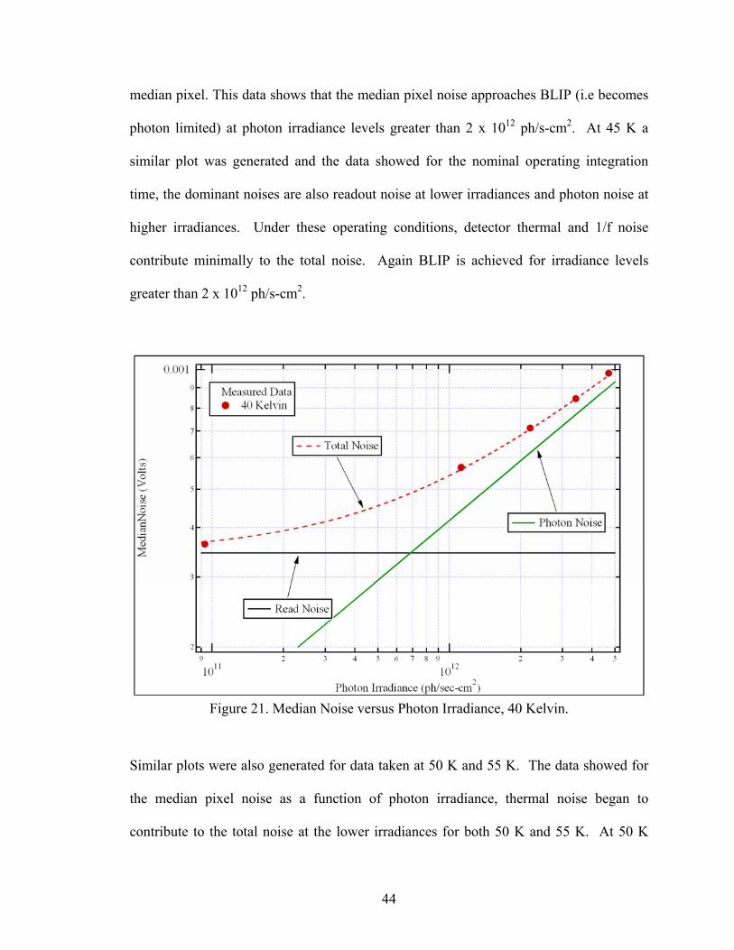
44
median pixel. This data shows that the median pixel noise approaches BLIP (i.e becomes
photon limited) at photon irradiance levels greater than 2 x 10¹² ph/s-cm2. At 45 K a
similar plot was generated and the data showed for the nominal operating integration
time, the dominant noises are also readout noise at lower irradiances and photon noise at
higher irradiances. Under these operating conditions, detector thermal and 1/f noise
contribute minimally to the total noise. Again BLIP is achieved for irradiance levels
greater than 2 x 10¹² ph/s-cm2.
Figure 21. Median Noise versus Photon Irradiance, 40 Kelvin.
Similar plots were also generated for data taken at 50 K and 55 K. The data showed for
the median pixel noise as a function of photon irradiance, thermal noise began to
contribute to the total noise at the lower irradiances for both 50 K and 55 K. At 50 K
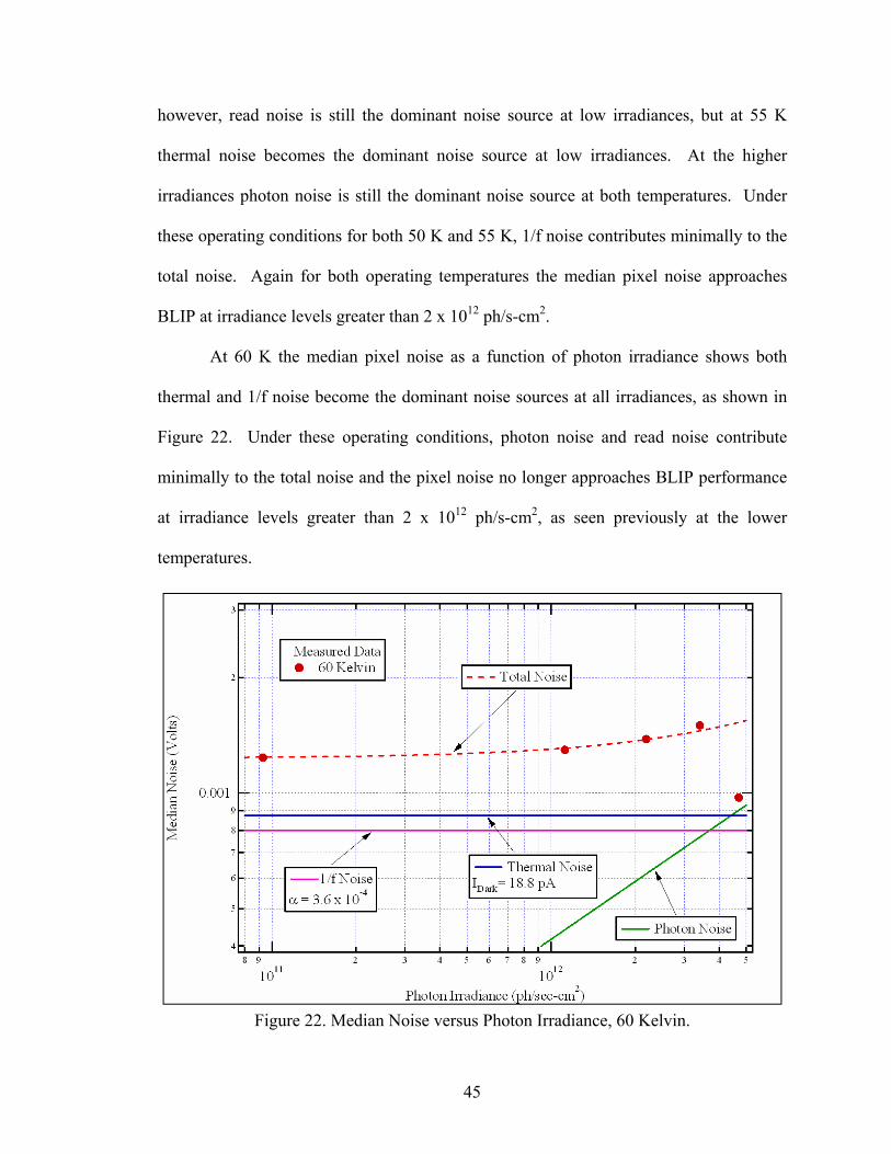
45
however, read noise is still the dominant noise source at low irradiances, but at 55 K
thermal noise becomes the dominant noise source at low irradiances. At the higher
irradiances photon noise is still the dominant noise source at both temperatures. Under
these operating conditions for both 50 K and 55 K, 1/f noise contributes minimally to the
total noise. Again for both operating temperatures the median pixel noise approaches
BLIP at irradiance levels greater than 2 x 10¹² ph/s-cm2.
At 60 K the median pixel noise as a function of photon irradiance shows both
thermal and 1/f noise become the dominant noise sources at all irradiances, as shown in
Figure 22. Under these operating conditions, photon noise and read noise contribute
minimally to the total noise and the pixel noise no longer approaches BLIP performance
at irradiance levels greater than 2 x 10¹² ph/s-cm2, as seen previously at the lower
temperatures.
Figure 22. Median Noise versus Photon Irradiance, 60 Kelvin.
46
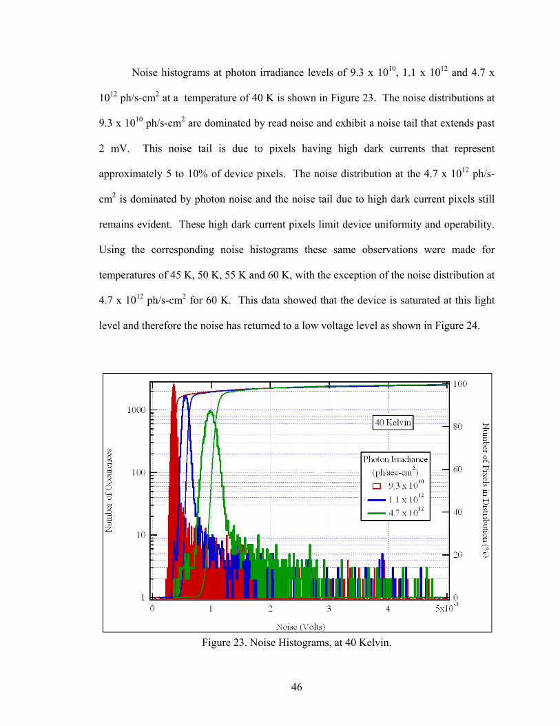
Noise histograms at photon irradiance levels of 9.3 x 10¹⁰, 1.1 x 10¹² and 4.7 x
1012 ph/s-cm2 at a temperature of 40 K is shown in Figure 23. The noise distributions at
9.3 x 10¹⁰ ph/s-cm2 are dominated by read noise and exhibit a noise tail that extends past
2 mV. This noise tail is due to pixels having high dark currents that represent
approximately 5 to 10% of device pixels. The noise distribution at the 4.7 x 10¹² ph/s-
cm2 is dominated by photon noise and the noise tail due to high dark current pixels still
remains evident. These high dark current pixels limit device uniformity and operability.
Using the corresponding noise histograms these same observations were made for
temperatures of 45 K, 50 K, 55 K and 60 K, with the exception of the noise distribution at
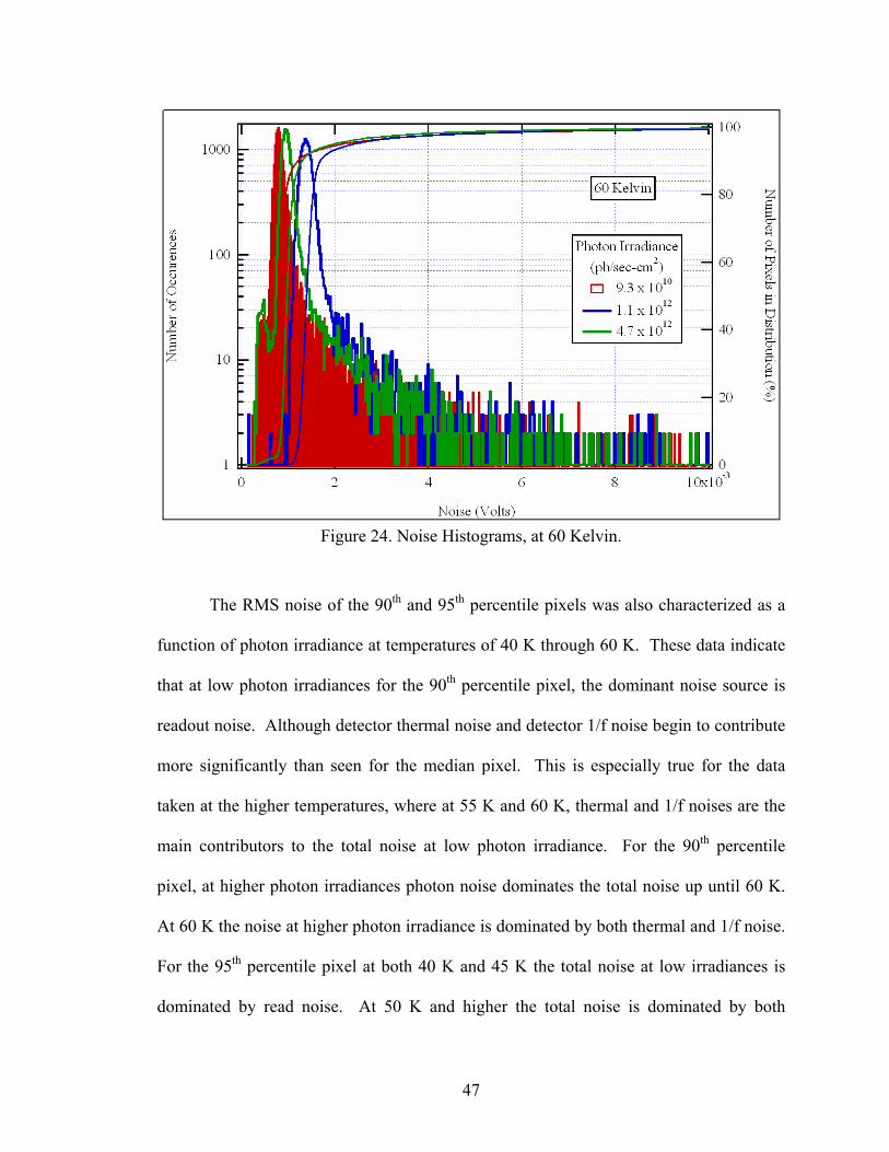
4.7 x 10¹² ph/s-cm2 for 60 K. This data showed that the device is saturated at this light
level and therefore the noise has returned to a low voltage level as shown in Figure 24.
Figure 23. Noise Histograms, at 40 Kelvin.
47
Figure 24. Noise Histograms, at 60 Kelvin.
The RMS noise of the 90th and 95th percentile pixels was also characterized as a
function of photon irradiance at temperatures of 40 K through 60 K. These data indicate
that at low photon irradiances for the 90th percentile pixel, the dominant noise source is
readout noise. Although detector thermal noise and detector 1/f noise begin to contribute
more significantly than seen for the median pixel. This is especially true for the data
taken at the higher temperatures, where at 55 K and 60 K, thermal and 1/f noises are the
main contributors to the total noise at low photon irradiance. For the 90th percentile
pixel, at higher photon irradiances photon noise dominates the total noise up until 60 K.
At 60 K the noise at higher photon irradiance is dominated by both thermal and 1/f noise.
For the 95th percentile pixel at both 40 K and 45 K the total noise at low irradiances is
dominated by read noise. At 50 K and higher the total noise is dominated by both
48
thermal and 1/f noise at low photon irradiances. For the higher photon irradiances the
noise is dominated by photon noise till 50 K where thermal and 1/f noise become the
dominant noise sources. The empirical parameter, α, which determines the detector 1/f
noise contribution, was determined for these noise data using the novel measurement
technique which will be described in detail in the next chapter.
Noise data was also taken as a function of integration time for the temperatures of
40 K through 60 K. Again pixels representing the median, 90th and 95th percentiles were
studied. These data are the basis for the novel 1/f noise measurement technique and will
be analyzed in detail in the next chapter.
2.3 Conventional Method
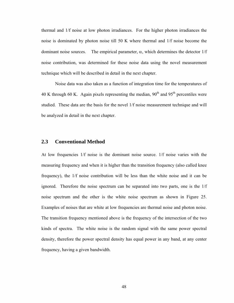
At low frequencies 1/f noise is the dominant noise source. 1/f noise varies with the
measuring frequency and when it is higher than the transition frequency (also called knee
frequency), the 1/f noise contribution will be less than the white noise and it can be
ignored. Therefore the noise spectrum can be separated into two parts, one is the 1/f
noise spectrum and the other is the white noise spectrum as shown in Figure 25.
Examples of noises that are white at low frequencies are thermal noise and photon noise.
The transition frequency mentioned above is the frequency of the intersection of the two
kinds of spectra. The white noise is the random signal with the same power spectral
density, therefore the power spectral density has equal power in any band, at any center
frequency, having a given bandwidth.
49
Figure 25. Noise Spectrum demonstrating both the 1/f noise and white noise spectra.
The shape of the power spectrum uniquely characterizes the process only if it is
stationary and Gaussian, all higher order correlation’s are zero. Measurements at low
frequencies become difficult due to drifts in the sample temperature and the patience of
the person taking the measurements, these factors can limit the accuracy of the data
collected.
The conventional method of measuring 1/f noise in detectors has been to collect
data for long periods of time and to analyze the frequency spectrum, which is why as
mentioned above the patience of the person taking the measurement could limit the
accuracy of the results. To verify the novel measurement technique the conventional data
was obtained for reference purposes. Long time histories were taken of the device output
under several operating conditions to demonstrate the dependencies of 1/f noise in
50
HgCdTe devices and to assist in the verification and understanding of the novel 1/f noise
measurement technique. The long time histories consist of data taken of the output
voltage in the time domain for a long integration time period for 20480 frames. This data
was taken simultaneously on 30 detectors to ensure 1/f noise would be observed in at
least one device and tractable as a function of the operating condition. The operating
conditions under which these measurements were taken include operating temperatures
from 40 K to 60 K, at several reverse bias voltages and as a function of photon irradiance.
Another approach to collecting this data would be to use a spectrum analyzer
(data still takes a long time to acquire and environment must be controlled), which
generates a plot of the spectral density as a function of frequency. The approach used for
this experiment is the preferred because the data is taken in the time domain, which is the
domain in which these devices are operated. In either approach a plot of the noise
spectral density as a function of frequency is the most complete and accurate way to
characterize 1/f noise.
To begin it is important to understand the general process of detecting an
electrical signal which starts with a detector and a readout circuit. The current caused by
the electrical signal is integrated on a capacitor for one integration time period and the
output voltage from one frame time on the capacitor is sampled and stored. The capacitor
is then reset and the process repeats. After the desired number of frames is completed the
stored set of samples is used to compute the average output and RMS noise for the
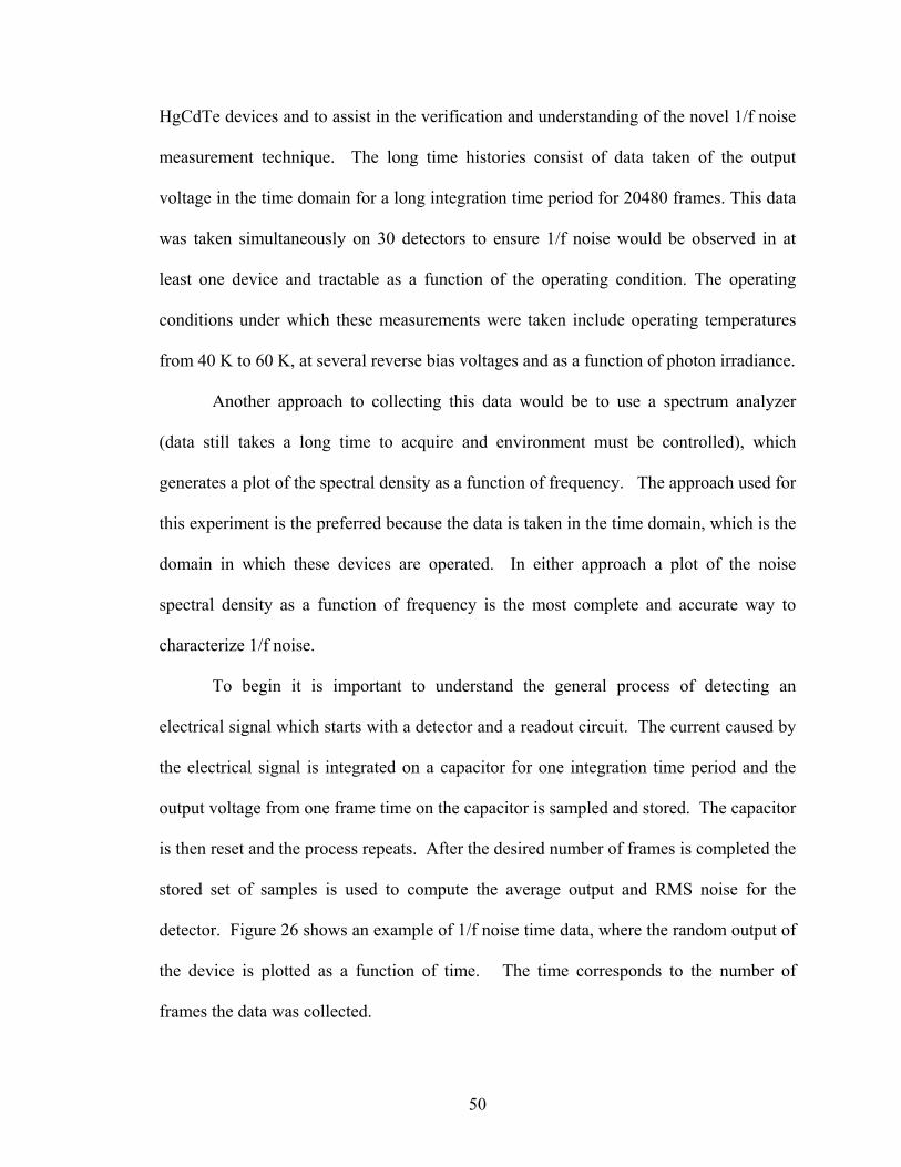
detector. Figure 26 shows an example of 1/f noise time data, where the random output of
the device is plotted as a function of time. The time corresponds to the number of
frames the data was collected.
51
Figure 26. 1/f Noise Time Data.
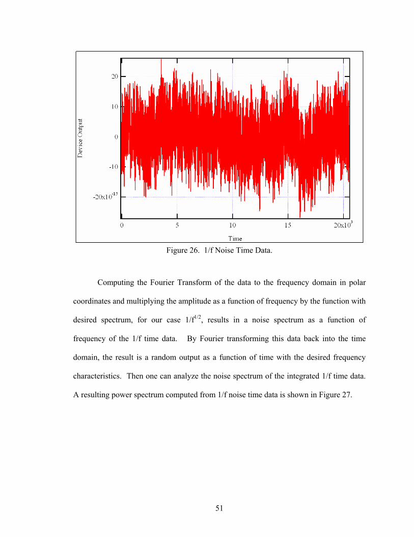
Computing the Fourier Transform of the data to the frequency domain in polar
coordinates and multiplying the amplitude as a function of frequency by the function with
desired spectrum, for our case 1/f1/2, results in a noise spectrum as a function of
frequency of the 1/f time data. By Fourier transforming this data back into the time
domain, the result is a random output as a function of time with the desired frequency
characteristics. Then one can analyze the noise spectrum of the integrated 1/f time data.
A resulting power spectrum computed from 1/f noise time data is shown in Figure 27.
52
Figure 27. Current Power Spectrum versus Frequency.
The frequency independent white noise of the noise spectrum can be described by the
following equation
RfkTI n
∆=
42 (29)
Where:
In = effective noise current (root mean square value), [Amps2]
4kT∆f = product represents a power, [Amp*Volt]
R = resistance value, [Ω]
By normalizing the power term 4kT∆f to ∆f (usually at 1 Hz), we end up with a power
53
density, which can be plotted against frequency.
RkT
fI n 42
=∆ (30)
This type of plot for the HgCdTe device exhibits frequency dependencies, i.e. 1/f noise.
Figure 27 shows a spectrum and is therefore referred to as the power spectral density. A
more appropriate term is referred to as the current power spectral density, Si [A2/Hz]. It
can also be referred to as the voltage power spectral density Sv [V2/Hz]. The square root
of Si or Sv is called the equivalent noise current [A/Hz-1/2] or the equivalent noise voltage
[V/Hz-1/2] respectively.
fIEnc n
∆=
2
(31)
A plot of the equivalent noise current corresponding to the current power spectral density
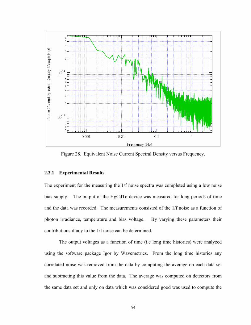
of Figure 27 is shown in Figure 28. From this data the 1/f noise contribution can be
determined. The next section describes this method of extracting the 1/f noise from the
current power spectral densities.
54
Figure 28. Equivalent Noise Current Spectral Density versus Frequency.
2.3.1 Experimental Results The experiment for the measuring the 1/f noise spectra was completed using a low noise
bias supply. The output of the HgCdTe device was measured for long periods of time
and the data was recorded. The measurements consisted of the 1/f noise as a function of
photon irradiance, temperature and bias voltage. By varying these parameters their
contributions if any to the 1/f noise can be determined.
The output voltages as a function of time (i.e long time histories) were analyzed
using the software package Igor by Wavemetrics. From the long time histories any
correlated noise was removed from the data by computing the average on each data set
and subtracting this value from the data. The average was computed on detectors from
the same data set and only on data which was considered good was used to compute the
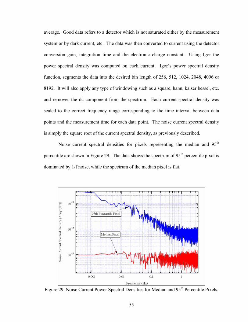
55
average. Good data refers to a detector which is not saturated either by the measurement
system or by dark current, etc. The data was then converted to current using the detector
conversion gain, integration time and the electronic charge constant. Using Igor the
power spectral density was computed on each current. Igor’s power spectral density
function, segments the data into the desired bin length of 256, 512, 1024, 2048, 4096 or
8192. It will also apply any type of windowing such as a square, hann, kaiser bessel, etc.
and removes the dc component from the spectrum. Each current spectral density was
scaled to the correct frequency range corresponding to the time interval between data
points and the measurement time for each data point. The noise current spectral density
is simply the square root of the current spectral density, as previously described.
Noise current spectral densities for pixels representing the median and 95th
percentile are shown in Figure 29. The data shows the spectrum of 95th percentile pixel is
dominated by 1/f noise, while the spectrum of the median pixel is flat.
Figure 29. Noise Current Power Spectral Densities for Median and 95th Percentile Pixels.
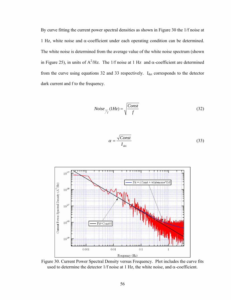
56
By curve fitting the current power spectral densities as shown in Figure 30 the 1/f noise at
1 Hz, white noise and α-coefficient under each operating condition can be determined.
The white noise is determined from the average value of the white noise spectrum (shown
in Figure 25), in units of A2/Hz. The 1/f noise at 1 Hz and α-coefficient are determined
from the curve using equations 32 and 33 respectively. Idet corresponds to the detector
dark current and f to the frequency.
fConstHzNoise
f=)1(1 (32)
detIConst
=α (33)
Figure 30. Current Power Spectral Density versus Frequency. Plot includes the curve fits
used to determine the detector 1/f noise at 1 Hz, the white noise, and α-coefficient.
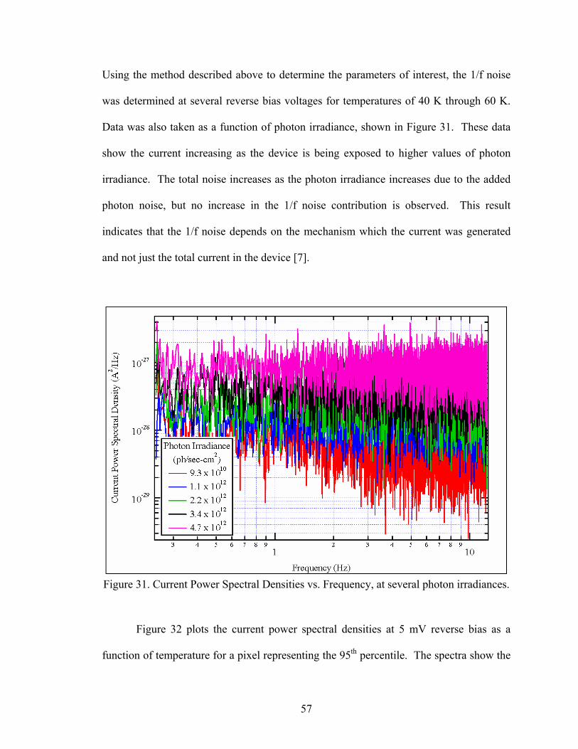
57
Using the method described above to determine the parameters of interest, the 1/f noise
was determined at several reverse bias voltages for temperatures of 40 K through 60 K.
Data was also taken as a function of photon irradiance, shown in Figure 31. These data
show the current increasing as the device is being exposed to higher values of photon
irradiance. The total noise increases as the photon irradiance increases due to the added
photon noise, but no increase in the 1/f noise contribution is observed. This result
indicates that the 1/f noise depends on the mechanism which the current was generated
and not just the total current in the device [7].
Figure 31. Current Power Spectral Densities vs. Frequency, at several photon irradiances.
Figure 32 plots the current power spectral densities at 5 mV reverse bias as a
function of temperature for a pixel representing the 95th percentile. The spectra show the
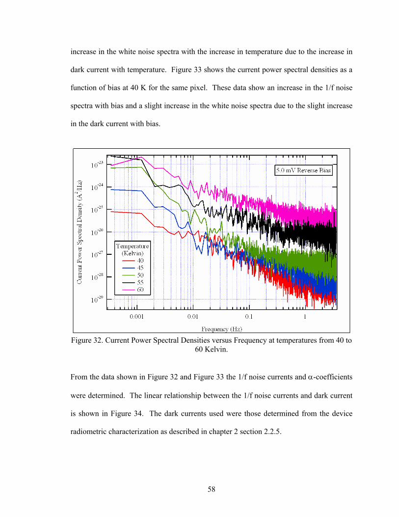
58
increase in the white noise spectra with the increase in temperature due to the increase in
dark current with temperature. Figure 33 shows the current power spectral densities as a
function of bias at 40 K for the same pixel. These data show an increase in the 1/f noise
spectra with bias and a slight increase in the white noise spectra due to the slight increase
in the dark current with bias.
Figure 32. Current Power Spectral Densities versus Frequency at temperatures from 40 to
60 Kelvin.
From the data shown in Figure 32 and Figure 33 the 1/f noise currents and α-coefficients
were determined. The linear relationship between the 1/f noise currents and dark current
is shown in Figure 34. The dark currents used were those determined from the device
radiometric characterization as described in chapter 2 section 2.2.5.
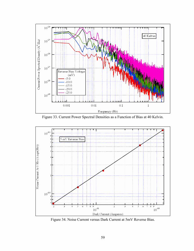
59
Figure 33. Current Power Spectral Densities as a Function of Bias at 40 Kelvin.
Figure 34. Noise Current versus Dark Current at 5mV Reverse Bias.
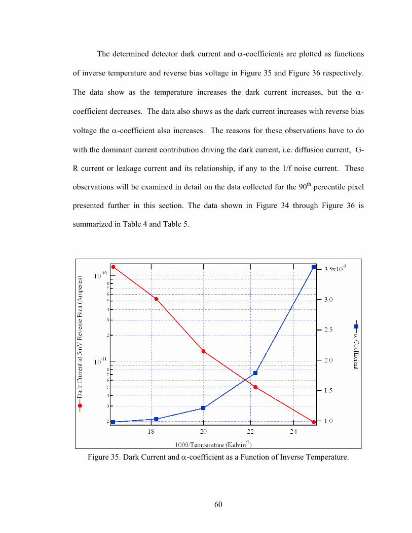
60
The determined detector dark current and α-coefficients are plotted as functions
of inverse temperature and reverse bias voltage in Figure 35 and Figure 36 respectively.
The data show as the temperature increases the dark current increases, but the α-
coefficient decreases. The data also shows as the dark current increases with reverse bias
voltage the α-coefficient also increases. The reasons for these observations have to do
with the dominant current contribution driving the dark current, i.e. diffusion current, G-
R current or leakage current and its relationship, if any to the 1/f noise current. These
observations will be examined in detail on the data collected for the 90th percentile pixel
presented further in this section. The data shown in Figure 34 through Figure 36 is
summarized in Table 4 and Table 5.
Figure 35. Dark Current and α-coefficient as a Function of Inverse Temperature.
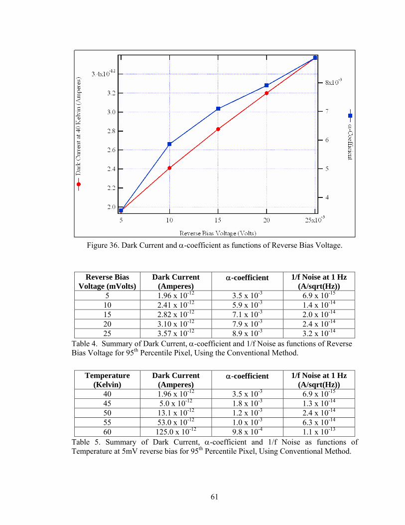
61
Figure 36. Dark Current and α-coefficient as functions of Reverse Bias Voltage.
Reverse Bias Voltage (mVolts)
Dark Current (Amperes)
α-coefficient 1/f Noise at 1 Hz (A/sqrt(Hz))
5 1.96 x 10⁻¹² 3.5 x 10⁻³ 6.9 x 10⁻¹⁵ 10 2.41 x 10⁻¹² 5.9 x 10⁻³ 1.4 x 10⁻¹⁴ 15 2.82 x 10⁻¹² 7.1 x 10⁻³ 2.0 x 10⁻¹⁴ 20 3.10 x 10⁻¹² 7.9 x 10⁻³ 2.4 x 10⁻¹⁴ 25 3.57 x 10⁻¹² 8.9 x 10⁻³ 3.2 x 10⁻¹⁴
Table 4. Summary of Dark Current, α-coefficient and 1/f Noise as functions of Reverse Bias Voltage for 95th Percentile Pixel, Using the Conventional Method.
Temperature
(Kelvin) Dark Current
(Amperes) α-coefficient 1/f Noise at 1 Hz
(A/sqrt(Hz)) 40 1.96 x 10⁻¹² 3.5 x 10⁻³ 6.9 x 10⁻¹⁵ 45 5.0 x 10⁻¹² 1.8 x 10⁻³ 1.3 x 10⁻¹⁴ 50 13.1 x 10⁻¹² 1.2 x 10⁻³ 2.4 x 10⁻¹⁴ 55 53.0 x 10⁻¹² 1.0 x 10⁻³ 6.3 x 10⁻¹⁴ 60 125.0 x 10⁻¹² 9.8 x 10⁻⁴ 1.1 x 10⁻¹³
Table 5. Summary of Dark Current, α-coefficient and 1/f Noise as functions of Temperature at 5mV reverse bias for 95th Percentile Pixel, Using Conventional Method.
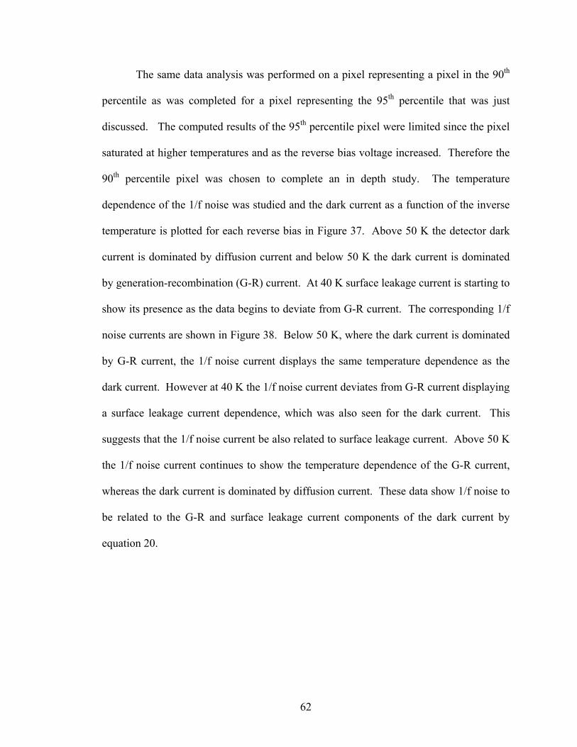
62
The same data analysis was performed on a pixel representing a pixel in the 90th
percentile as was completed for a pixel representing the 95th percentile that was just
discussed. The computed results of the 95th percentile pixel were limited since the pixel
saturated at higher temperatures and as the reverse bias voltage increased. Therefore the
90th percentile pixel was chosen to complete an in depth study. The temperature
dependence of the 1/f noise was studied and the dark current as a function of the inverse
temperature is plotted for each reverse bias in Figure 37. Above 50 K the detector dark
current is dominated by diffusion current and below 50 K the dark current is dominated
by generation-recombination (G-R) current. At 40 K surface leakage current is starting to
show its presence as the data begins to deviate from G-R current. The corresponding 1/f
noise currents are shown in Figure 38. Below 50 K, where the dark current is dominated
by G-R current, the 1/f noise current displays the same temperature dependence as the
dark current. However at 40 K the 1/f noise current deviates from G-R current displaying
a surface leakage current dependence, which was also seen for the dark current. This
suggests that the 1/f noise current be also related to surface leakage current. Above 50 K
the 1/f noise current continues to show the temperature dependence of the G-R current,
whereas the dark current is dominated by diffusion current. These data show 1/f noise to
be related to the G-R and surface leakage current components of the dark current by
equation 20.
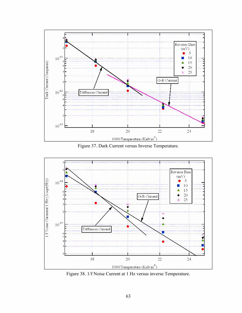
63
Figure 37. Dark Current versus Inverse Temperature.
Figure 38. 1/f Noise Current at 1 Hz versus inverse Temperature.
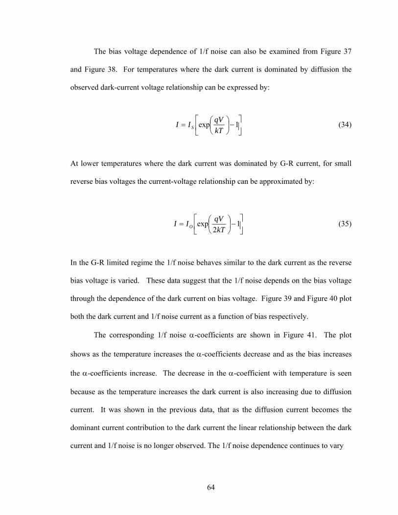
64
The bias voltage dependence of 1/f noise can also be examined from Figure 37
and Figure 38. For temperatures where the dark current is dominated by diffusion the
observed dark-current voltage relationship can be expressed by:
⎥⎦
⎤⎢⎣
⎡−⎟
⎠⎞
⎜⎝⎛= 1exp
kTqVII S (34)
At lower temperatures where the dark current was dominated by G-R current, for small
reverse bias voltages the current-voltage relationship can be approximated by:
⎥⎦
⎤⎢⎣
⎡−⎟
⎠⎞
⎜⎝⎛= 1
2exp
kTqVII O (35)
In the G-R limited regime the 1/f noise behaves similar to the dark current as the reverse
bias voltage is varied. These data suggest that the 1/f noise depends on the bias voltage
through the dependence of the dark current on bias voltage. Figure 39 and Figure 40 plot
both the dark current and 1/f noise current as a function of bias respectively.
The corresponding 1/f noise α-coefficients are shown in Figure 41. The plot
shows as the temperature increases the α-coefficients decrease and as the bias increases
the α-coefficients increase. The decrease in the α-coefficient with temperature is seen
because as the temperature increases the dark current is also increasing due to diffusion
current. It was shown in the previous data, that as the diffusion current becomes the
dominant current contribution to the dark current the linear relationship between the dark
current and 1/f noise is no longer observed. The 1/f noise dependence continues to vary
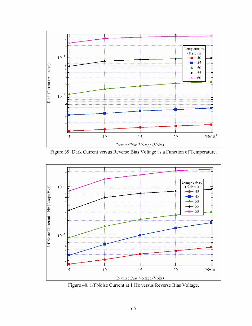
65
Figure 39. Dark Current versus Reverse Bias Voltage as a Function of Temperature.
Figure 40. 1/f Noise Current at 1 Hz versus Reverse Bias Voltage.
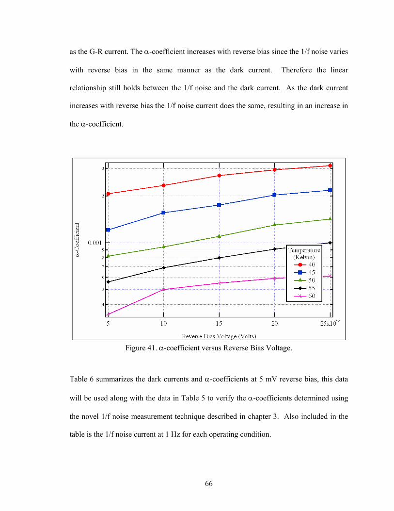
66
as the G-R current. The α-coefficient increases with reverse bias since the 1/f noise varies
with reverse bias in the same manner as the dark current. Therefore the linear
relationship still holds between the 1/f noise and the dark current. As the dark current
increases with reverse bias the 1/f noise current does the same, resulting in an increase in
the α-coefficient.
Figure 41. α-coefficient versus Reverse Bias Voltage.
Table 6 summarizes the dark currents and α-coefficients at 5 mV reverse bias, this data
will be used along with the data in Table 5 to verify the α-coefficients determined using
the novel 1/f noise measurement technique described in chapter 3. Also included in the
table is the 1/f noise current at 1 Hz for each operating condition.
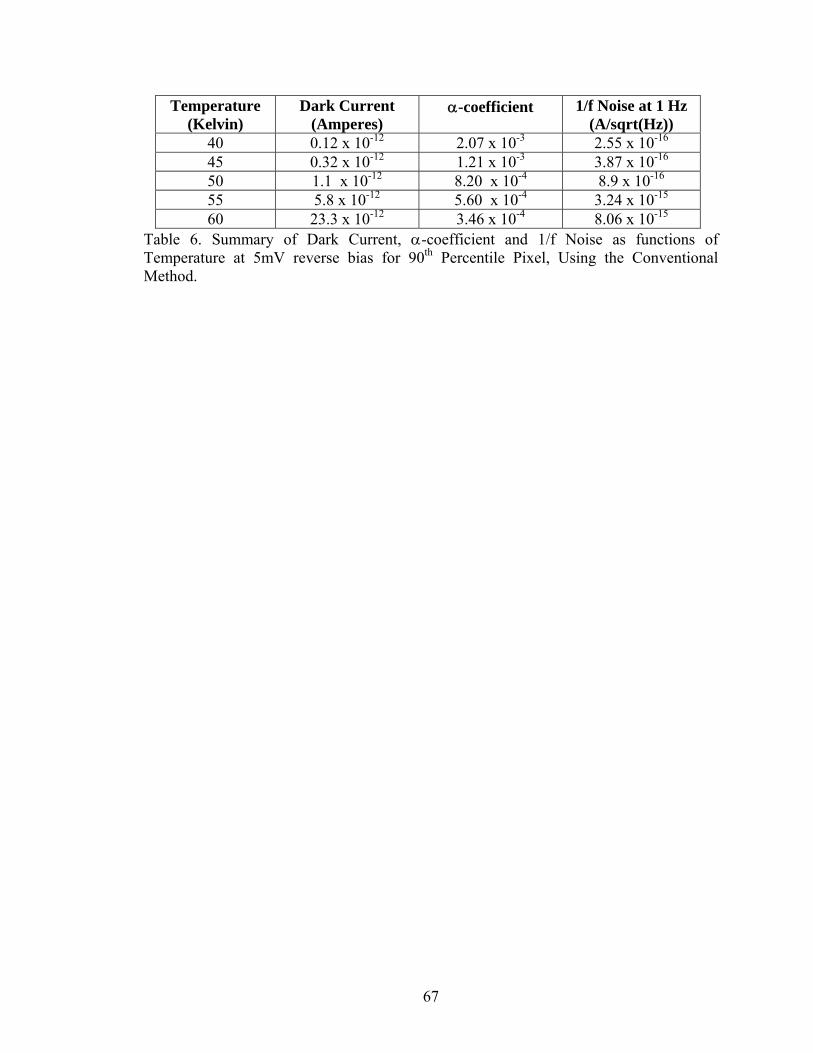
67
Temperature (Kelvin)
Dark Current (Amperes)
α-coefficient 1/f Noise at 1 Hz (A/sqrt(Hz))
40 0.12 x 10⁻¹² 2.07 x 10⁻³ 2.55 x 10⁻¹⁶ 45 0.32 x 10⁻¹² 1.21 x 10⁻³ 3.87 x 10⁻¹⁶ 50 1.1 x 10⁻¹² 8.20 x 10⁻⁴ 8.9 x 10⁻¹⁶ 55 5.8 x 10⁻¹² 5.60 x 10⁻⁴ 3.24 x 10⁻¹⁵ 60 23.3 x 10⁻¹² 3.46 x 10⁻⁴ 8.06 x 10⁻¹⁵
Table 6. Summary of Dark Current, α-coefficient and 1/f Noise as functions of Temperature at 5mV reverse bias for 90th Percentile Pixel, Using the Conventional Method.
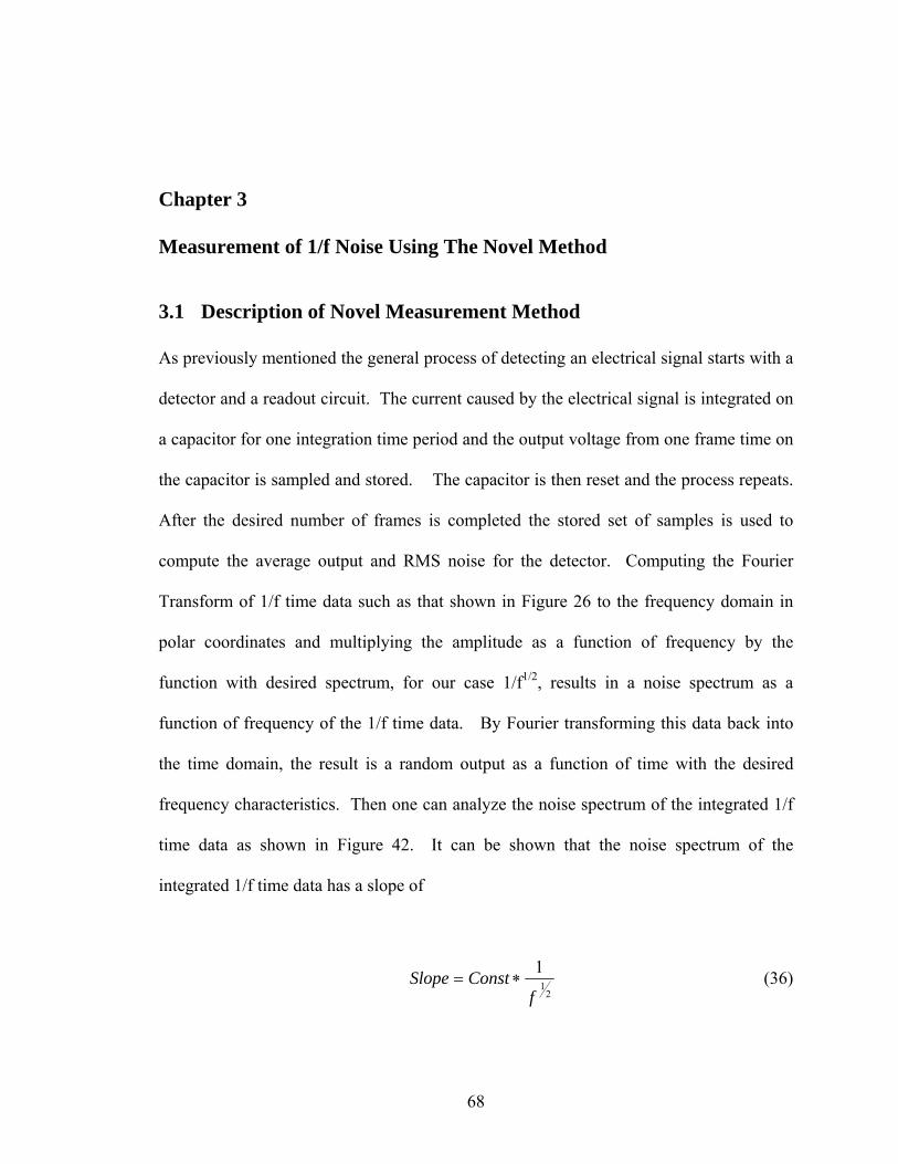
68
Chapter 3 Measurement of 1/f Noise Using The Novel Method
3.1 Description of Novel Measurement Method As previously mentioned the general process of detecting an electrical signal starts with a
detector and a readout circuit. The current caused by the electrical signal is integrated on
a capacitor for one integration time period and the output voltage from one frame time on
the capacitor is sampled and stored. The capacitor is then reset and the process repeats.
After the desired number of frames is completed the stored set of samples is used to
compute the average output and RMS noise for the detector. Computing the Fourier
Transform of 1/f time data such as that shown in Figure 26 to the frequency domain in
polar coordinates and multiplying the amplitude as a function of frequency by the
function with desired spectrum, for our case 1/f1/2, results in a noise spectrum as a
function of frequency of the 1/f time data. By Fourier transforming this data back into
the time domain, the result is a random output as a function of time with the desired
frequency characteristics. Then one can analyze the noise spectrum of the integrated 1/f
time data as shown in Figure 42. It can be shown that the noise spectrum of the
integrated 1/f time data has a slope of
21
1
fConstSlope ∗= (36)
69
with a constant of approximately 0.5.
Figure 42. Current Noise Spectral Density of Integrated Time Data.
Now suppose one applies the same theory, and computes the noise spectral
density for a random Gaussian output as shown in Figure 43. First, compute the Fourier
transform of the Gaussian into the frequency domain in polar coordinates and multiply
the amplitude as a function of frequency by one, which is the desired spectrum for a
Gaussian as shown in Figure 44. Fourier transform the data back into the time domain
and the result is a random output as a function of time with the desired frequency
characteristics, shown in Figure 45.
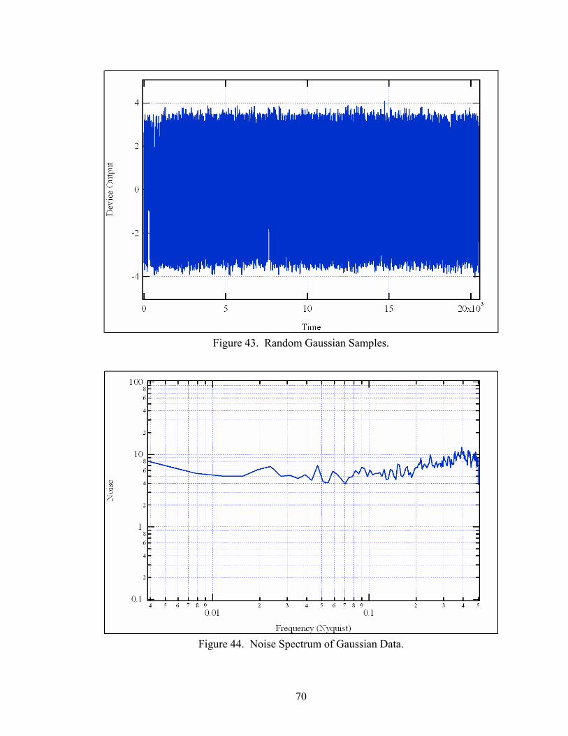
70
Figure 43. Random Gaussian Samples.
Figure 44. Noise Spectrum of Gaussian Data.
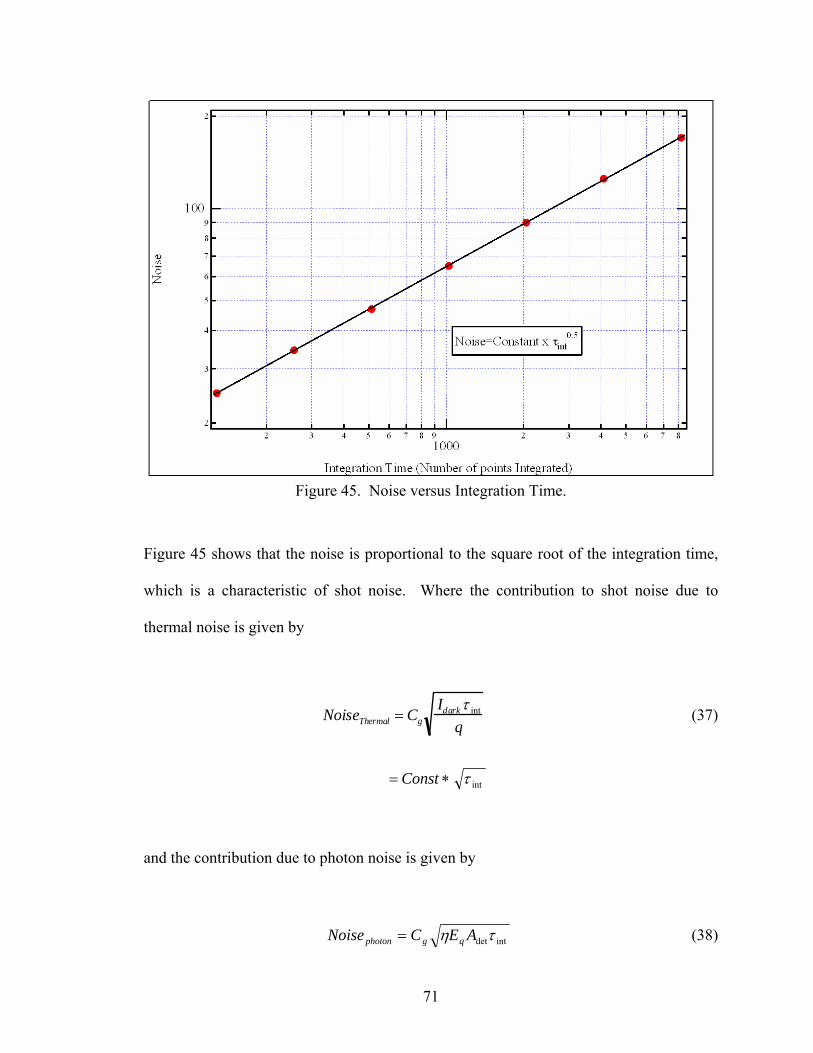
71
Figure 45. Noise versus Integration Time.
Figure 45 shows that the noise is proportional to the square root of the integration time,
which is a characteristic of shot noise. Where the contribution to shot noise due to
thermal noise is given by
NoiseThermal = Cg
Idarkτ int
q (37)
intτ∗= Const
and the contribution due to photon noise is given by
intdetτη AECNoise qgphoton = (38)
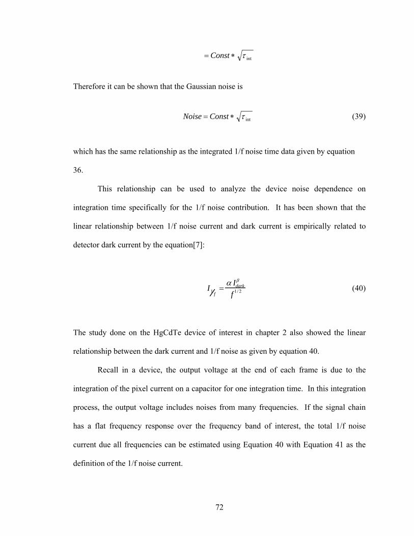
72
intτ∗= Const
Therefore it can be shown that the Gaussian noise is
intτ∗= ConstNoise (39)
which has the same relationship as the integrated 1/f noise time data given by equation
36.
This relationship can be used to analyze the device noise dependence on
integration time specifically for the 1/f noise contribution. It has been shown that the
linear relationship between 1/f noise current and dark current is empirically related to
detector dark current by the equation[7]:
I1 f=
α Idarkβ
f 1/ 2 (40)
The study done on the HgCdTe device of interest in chapter 2 also showed the linear
relationship between the dark current and 1/f noise as given by equation 40.
Recall in a device, the output voltage at the end of each frame is due to the
integration of the pixel current on a capacitor for one integration time. In this integration
process, the output voltage includes noises from many frequencies. If the signal chain
has a flat frequency response over the frequency band of interest, the total 1/f noise
current due all frequencies can be estimated using Equation 40 with Equation 41 as the
definition of the 1/f noise current.
73
I 1f ,total
=α Idark
f1
2
⎛
⎝ ⎜
⎞
⎠ ⎟
2
dff1
f2
∫⎡
⎣
⎢ ⎢
⎤
⎦
⎥ ⎥
12
(41)
Where:
f1 = 1/TR (Hz)
f2 = 1/(2τ) (Hz)
TR = re-calibration time or measurement time (seconds)
τ = integration time (seconds)
The re-calibration time is the time period over which data are taken to compute the noise
(standard deviation of the data). The re-calibration time is thus 100 (number of frames)
times the device frame time. The noise voltage produced by this current is proportional
to the readout conversion gain, the integration time and 1/electron charge as given below.
totalfg
totalnoise Iq
CV ,/1
int, ⎟⎟
⎠
⎞⎜⎜⎝
⎛=
τ (42)
Integrating I1/f,total gives the expression:
( ) ⎟⎟⎠
⎞⎜⎜⎝
⎛⎟⎟⎠
⎞⎜⎜⎝
⎛=
intint, 2
lnτ
τα Rgdark
totalnoiseT
qCI
V (43)
Where:
Cg = Conversion gain (V/electron)
τint = integration time (seconds)
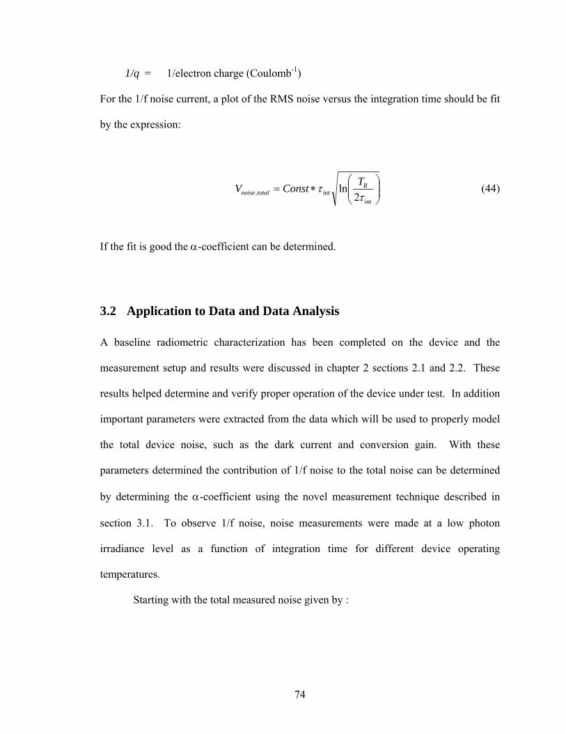
74
1/q = 1/electron charge (Coulomb-1)
For the 1/f noise current, a plot of the RMS noise versus the integration time should be fit
by the expression:
⎟⎟⎠
⎞⎜⎜⎝
⎛∗=
intint, 2
lnτ
τ Rtotalnoise
TConstV (44)
If the fit is good the α-coefficient can be determined.
3.2 Application to Data and Data Analysis
A baseline radiometric characterization has been completed on the device and the
measurement setup and results were discussed in chapter 2 sections 2.1 and 2.2. These
results helped determine and verify proper operation of the device under test. In addition
important parameters were extracted from the data which will be used to properly model
the total device noise, such as the dark current and conversion gain. With these
parameters determined the contribution of 1/f noise to the total noise can be determined
by determining the α-coefficient using the novel measurement technique described in
section 3.1. To observe 1/f noise, noise measurements were made at a low photon
irradiance level as a function of integration time for different device operating
temperatures.
Starting with the total measured noise given by :
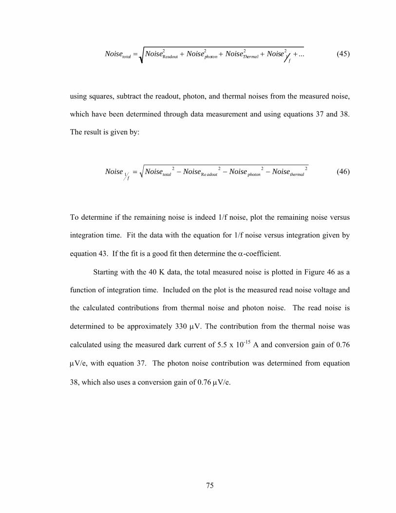
75
Noisetotal = NoiseReadout
2 + Noisephoton2 + NoiseThermal
2 + Noise 1f
2 + ... (45)
using squares, subtract the readout, photon, and thermal noises from the measured noise,
which have been determined through data measurement and using equations 37 and 38.
The result is given by:
222Re
21 thermalphotonadouttotal
fNoiseNoiseNoiseNoiseNoise −−−= (46)
To determine if the remaining noise is indeed 1/f noise, plot the remaining noise versus
integration time. Fit the data with the equation for 1/f noise versus integration given by
equation 43. If the fit is a good fit then determine the α-coefficient.
Starting with the 40 K data, the total measured noise is plotted in Figure 46 as a
function of integration time. Included on the plot is the measured read noise voltage and
the calculated contributions from thermal noise and photon noise. The read noise is
determined to be approximately 330 µV. The contribution from the thermal noise was
calculated using the measured dark current of 5.5 x 10⁻¹⁵ A and conversion gain of 0.76
µV/e, with equation 37. The photon noise contribution was determined from equation
38, which also uses a conversion gain of 0.76 µV/e.
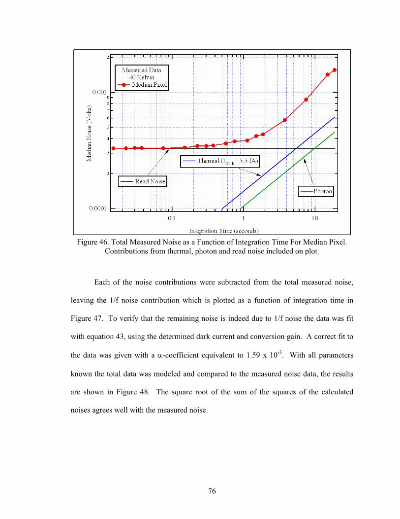
76
Figure 46. Total Measured Noise as a Function of Integration Time For Median Pixel.
Contributions from thermal, photon and read noise included on plot.
Each of the noise contributions were subtracted from the total measured noise,
leaving the 1/f noise contribution which is plotted as a function of integration time in
Figure 47. To verify that the remaining noise is indeed due to 1/f noise the data was fit
with equation 43, using the determined dark current and conversion gain. A correct fit to
the data was given with a α-coefficient equivalent to 1.59 x 10⁻³. With all parameters
known the total data was modeled and compared to the measured noise data, the results
are shown in Figure 48. The square root of the sum of the squares of the calculated
noises agrees well with the measured noise.
77
Figure 47. Remaining 1/f Noise versus integration Time.
Figure 48. Measured Noise versus Integration Time. Plot includes the total modeled
noise determined from all noise contributions.
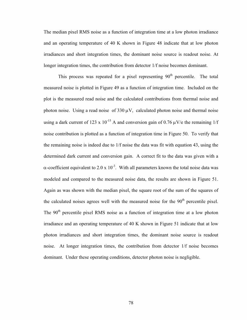
78
The median pixel RMS noise as a function of integration time at a low photon irradiance
and an operating temperature of 40 K shown in Figure 48 indicate that at low photon
irradiances and short integration times, the dominant noise source is readout noise. At
longer integration times, the contribution from detector 1/f noise becomes dominant.
This process was repeated for a pixel representing 90th percentile. The total
measured noise is plotted in Figure 49 as a function of integration time. Included on the
plot is the measured read noise and the calculated contributions from thermal noise and
photon noise. Using a read noise of 330 µV, calculated photon noise and thermal noise
using a dark current of 123 x 10-15 A and conversion gain of 0.76 µV/e the remaining 1/f
noise contribution is plotted as a function of integration time in Figure 50. To verify that
the remaining noise is indeed due to 1/f noise the data was fit with equation 43, using the
determined dark current and conversion gain. A correct fit to the data was given with a
α-coefficient equivalent to 2.0 x 10⁻³. With all parameters known the total noise data was
modeled and compared to the measured noise data, the results are shown in Figure 51.
Again as was shown with the median pixel, the square root of the sum of the squares of
the calculated noises agrees well with the measured noise for the 90th percentile pixel.
The 90th percentile pixel RMS noise as a function of integration time at a low photon
irradiance and an operating temperature of 40 K shown in Figure 51 indicate that at low
photon irradiances and short integration times, the dominant noise source is readout
noise. At longer integration times, the contribution from detector 1/f noise becomes
dominant. Under these operating conditions, detector photon noise is negligible.
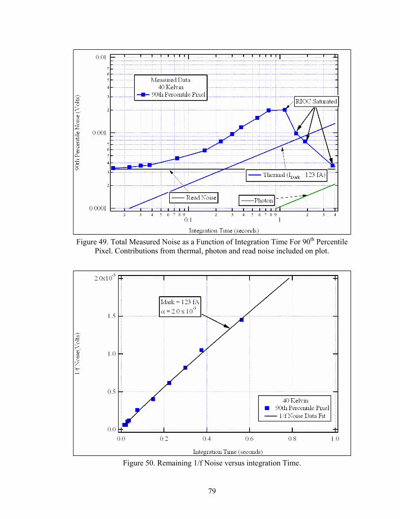
79
Figure 49. Total Measured Noise as a Function of Integration Time For 90th Percentile
Pixel. Contributions from thermal, photon and read noise included on plot.
Figure 50. Remaining 1/f Noise versus integration Time.
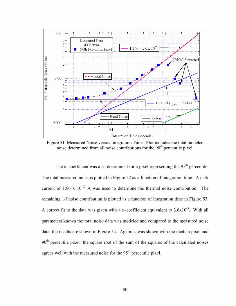
80
Figure 51. Measured Noise versus Integration Time. Plot includes the total modeled
noise determined from all noise contributions for the 90th percentile pixel.
The α-coefficient was also determined for a pixel representing the 95th percentile.
The total measured noise is plotted in Figure 52 as a function of integration time. A dark
current of 1.96 x 10⁻¹² A was used to determine the thermal noise contribution. The
remaining 1/f noise contribution is plotted as a function of integration time in Figure 53.
A correct fit to the data was given with a α-coefficient equivalent to 3.6x10⁻³. With all
parameters known the total noise data was modeled and compared to the measured noise
data, the results are shown in Figure 54. Again as was shown with the median pixel and
90th percentile pixel the square root of the sum of the squares of the calculated noises
agrees well with the measured noise for the 95th percentile pixel.
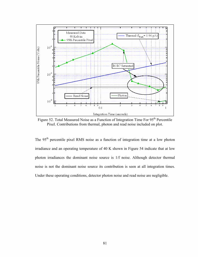
81
Figure 52. Total Measured Noise as a Function of Integration Time For 95th Percentile
Pixel. Contributions from thermal, photon and read noise included on plot.
The 95th percentile pixel RMS noise as a function of integration time at a low photon
irradiance and an operating temperature of 40 K shown in Figure 54 indicate that at low
photon irradiances the dominant noise source is 1/f noise. Although detector thermal
noise is not the dominant noise source its contribution is seen at all integration times.
Under these operating conditions, detector photon noise and read noise are negligible.
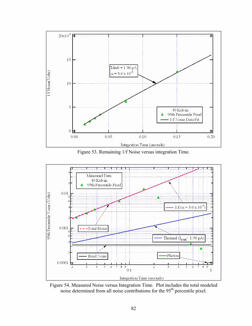
82
Figure 53. Remaining 1/f Noise versus integration Time.
Figure 54. Measured Noise versus Integration Time. Plot includes the total modeled
noise determined from all noise contributions for the 95th percentile pixel.
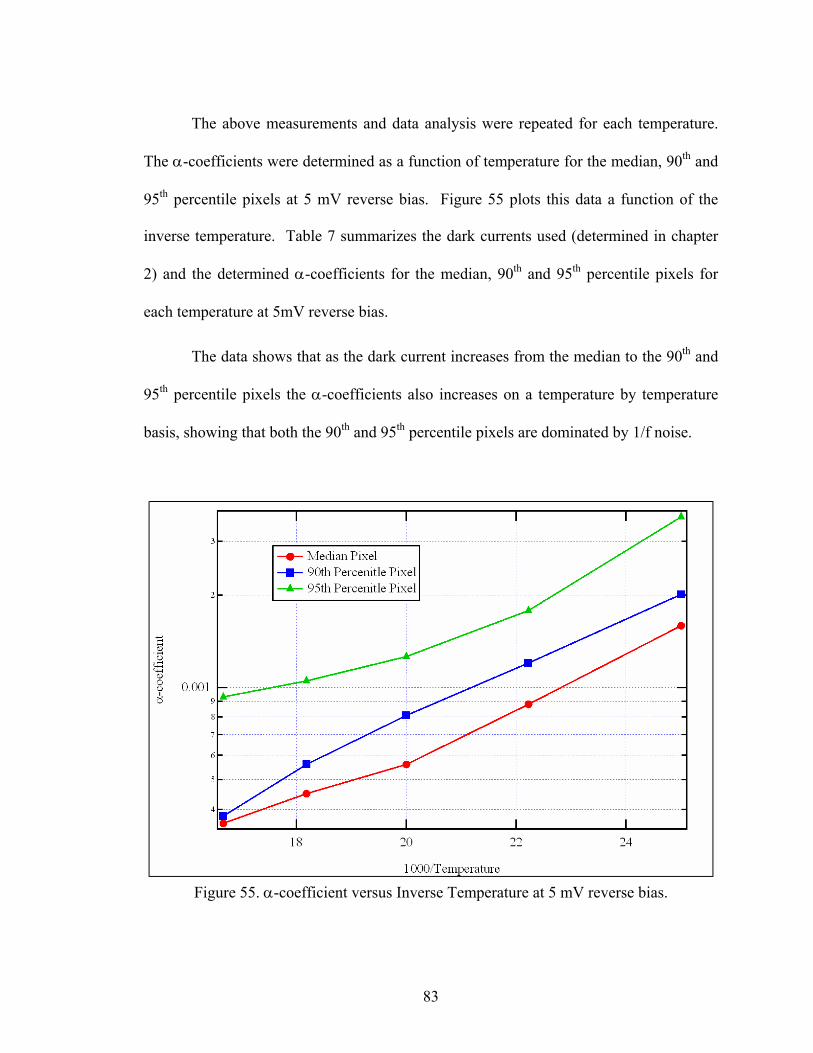
83
The above measurements and data analysis were repeated for each temperature.
The α-coefficients were determined as a function of temperature for the median, 90th and
95th percentile pixels at 5 mV reverse bias. Figure 55 plots this data a function of the
inverse temperature. Table 7 summarizes the dark currents used (determined in chapter
2) and the determined α-coefficients for the median, 90th and 95th percentile pixels for
each temperature at 5mV reverse bias.
The data shows that as the dark current increases from the median to the 90th and
95th percentile pixels the α-coefficients also increases on a temperature by temperature
basis, showing that both the 90th and 95th percentile pixels are dominated by 1/f noise.
Figure 55. α-coefficient versus Inverse Temperature at 5 mV reverse bias.
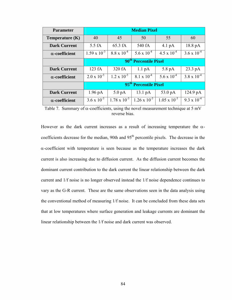
84
Parameter Median Pixel
Temperature (K) 40 45 50 55 60
Dark Current 5.5 fA 65.3 fA 540 fA 4.1 pA 18.8 pA
α-coefficient 1.59 x 10⁻³ 8.8 x 10⁻⁴ 5.6 x 10⁻⁴ 4.5 x 10⁻⁴ 3.6 x 10⁻⁴
90th Percentile Pixel
Dark Current 123 fA 320 fA 1.1 pA 5.8 pA 23.3 pA
α-coefficient 2.0 x 10⁻³ 1.2 x 10⁻³ 8.1 x 10⁻⁴ 5.6 x 10⁻⁴ 3.8 x 10⁻⁴
95th Percentile Pixel
Dark Current 1.96 pA 5.0 pA 13.1 pA 53.0 pA 124.9 pA
α-coefficient 3.6 x 10⁻³ 1.78 x 10⁻³ 1.26 x 10⁻³ 1.05 x 10⁻³ 9.3 x 10⁻⁴
Table 7. Summary of α-coefficients, using the novel measurement technique at 5 mV reverse bias.
However as the dark current increases as a result of increasing temperature the α-
coefficients decrease for the median, 90th and 95th percentile pixels. The decrease in the
α-coefficient with temperature is seen because as the temperature increases the dark
current is also increasing due to diffusion current. As the diffusion current becomes the
dominant current contribution to the dark current the linear relationship between the dark
current and 1/f noise is no longer observed instead the 1/f noise dependence continues to
vary as the G-R current. These are the same observations seen in the data analysis using
the conventional method of measuring 1/f noise. It can be concluded from these data sets
that at low temperatures where surface generation and leakage currents are dominant the
linear relationship between the 1/f noise and dark current was observed.
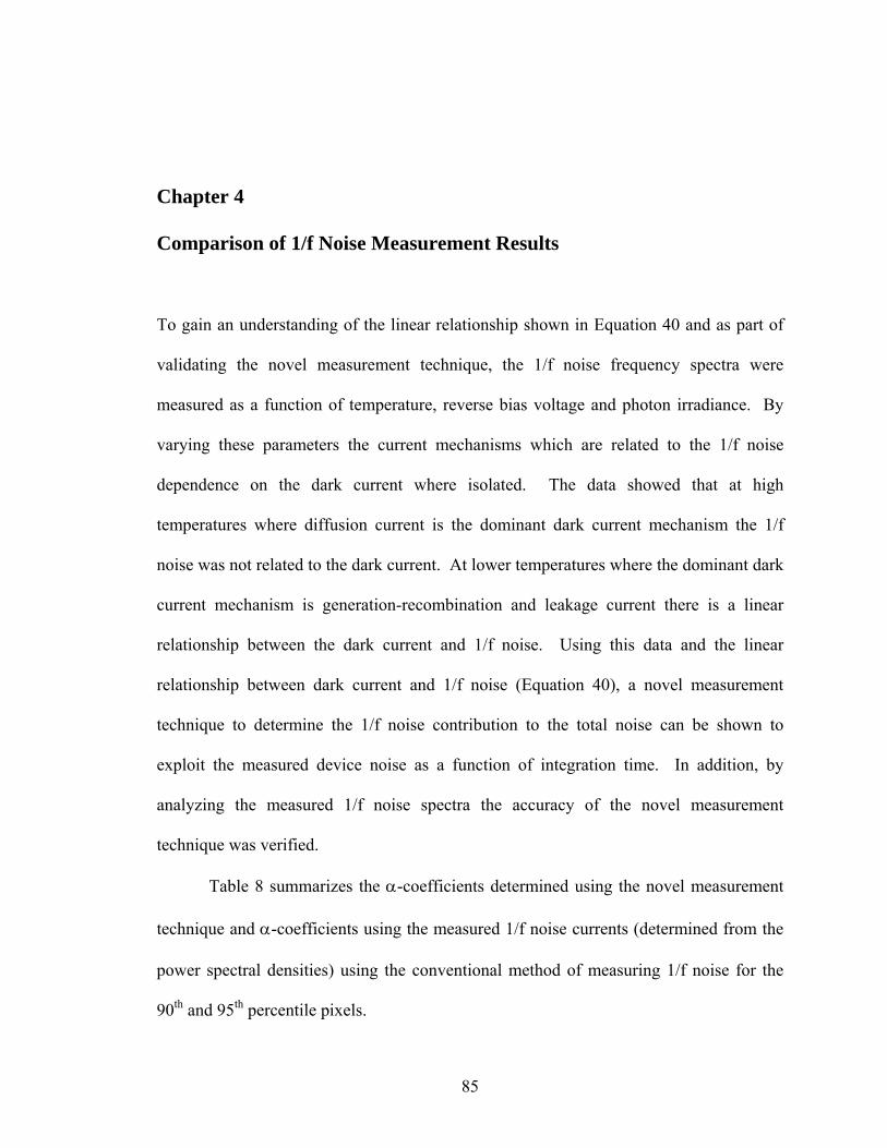
85
Chapter 4 Comparison of 1/f Noise Measurement Results To gain an understanding of the linear relationship shown in Equation 40 and as part of
validating the novel measurement technique, the 1/f noise frequency spectra were
measured as a function of temperature, reverse bias voltage and photon irradiance. By
varying these parameters the current mechanisms which are related to the 1/f noise
dependence on the dark current where isolated. The data showed that at high
temperatures where diffusion current is the dominant dark current mechanism the 1/f
noise was not related to the dark current. At lower temperatures where the dominant dark
current mechanism is generation-recombination and leakage current there is a linear
relationship between the dark current and 1/f noise. Using this data and the linear
relationship between dark current and 1/f noise (Equation 40), a novel measurement
technique to determine the 1/f noise contribution to the total noise can be shown to
exploit the measured device noise as a function of integration time. In addition, by
analyzing the measured 1/f noise spectra the accuracy of the novel measurement
technique was verified.
Table 8 summarizes the α-coefficients determined using the novel measurement
technique and α-coefficients using the measured 1/f noise currents (determined from the
power spectral densities) using the conventional method of measuring 1/f noise for the
90th and 95th percentile pixels.
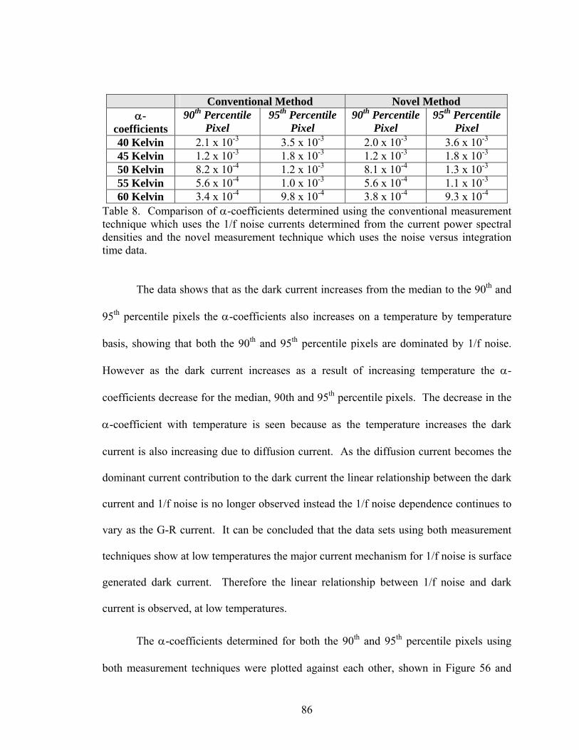
86
Conventional Method Novel Method α-
coefficients 90th Percentile
Pixel 95th Percentile
Pixel 90th Percentile
Pixel 95th Percentile
Pixel 40 Kelvin 2.1 x 10⁻³ 3.5 x 10⁻³ 2.0 x 10⁻³ 3.6 x 10⁻³ 45 Kelvin 1.2 x 10⁻³ 1.8 x 10⁻³ 1.2 x 10⁻³ 1.8 x 10⁻³ 50 Kelvin 8.2 x 10⁻⁴ 1.2 x 10⁻³ 8.1 x 10⁻⁴ 1.3 x 10⁻³ 55 Kelvin 5.6 x 10⁻⁴ 1.0 x 10⁻³ 5.6 x 10⁻⁴ 1.1 x 10⁻³ 60 Kelvin 3.4 x 10⁻⁴ 9.8 x 10⁻⁴ 3.8 x 10⁻⁴ 9.3 x 10⁻⁴
Table 8. Comparison of α-coefficients determined using the conventional measurement technique which uses the 1/f noise currents determined from the current power spectral densities and the novel measurement technique which uses the noise versus integration time data.
The data shows that as the dark current increases from the median to the 90th and
95th percentile pixels the α-coefficients also increases on a temperature by temperature
basis, showing that both the 90th and 95th percentile pixels are dominated by 1/f noise.
However as the dark current increases as a result of increasing temperature the α-
coefficients decrease for the median, 90th and 95th percentile pixels. The decrease in the
α-coefficient with temperature is seen because as the temperature increases the dark
current is also increasing due to diffusion current. As the diffusion current becomes the
dominant current contribution to the dark current the linear relationship between the dark
current and 1/f noise is no longer observed instead the 1/f noise dependence continues to
vary as the G-R current. It can be concluded that the data sets using both measurement
techniques show at low temperatures the major current mechanism for 1/f noise is surface
generated dark current. Therefore the linear relationship between 1/f noise and dark
current is observed, at low temperatures.
The α-coefficients determined for both the 90th and 95th percentile pixels using
both measurement techniques were plotted against each other, shown in Figure 56 and
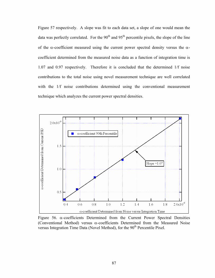
87
Figure 57 respectively. A slope was fit to each data set, a slope of one would mean the
data was perfectly correlated. For the 90th and 95th percentile pixels, the slope of the line
of the α-coefficient measured using the current power spectral density versus the α-
coefficient determined from the measured noise data as a function of integration time is
1.07 and 0.97 respectively. Therefore it is concluded that the determined 1/f noise
contributions to the total noise using novel measurement technique are well correlated
with the 1/f noise contributions determined using the conventional measurement
technique which analyzes the current power spectral densities.
Figure 56. α-coefficients Determined from the Current Power Spectral Densities (Conventional Method) versus α-coefficients Determined from the Measured Noise versus Integration Time Data (Novel Method), for the 90th Percentile Pixel.
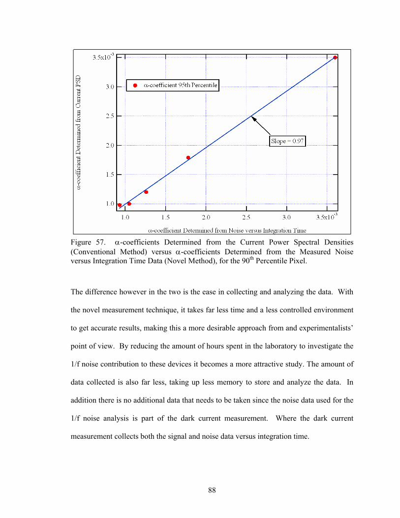
88
Figure 57. α-coefficients Determined from the Current Power Spectral Densities (Conventional Method) versus α-coefficients Determined from the Measured Noise versus Integration Time Data (Novel Method), for the 90th Percentile Pixel.
The difference however in the two is the ease in collecting and analyzing the data. With
the novel measurement technique, it takes far less time and a less controlled environment
to get accurate results, making this a more desirable approach from and experimentalists’
point of view. By reducing the amount of hours spent in the laboratory to investigate the
1/f noise contribution to these devices it becomes a more attractive study. The amount of
data collected is also far less, taking up less memory to store and analyze the data. In
addition there is no additional data that needs to be taken since the noise data used for the
1/f noise analysis is part of the dark current measurement. Where the dark current
measurement collects both the signal and noise data versus integration time.
89
Chapter 5
Conclusions and Future Work
Determining and understanding the 1/f noise in HgCdTe devices is significantly
important. First this noise mechanism is a contributor to degraded performance by
decreasing the device sensitivity. In addition 1/f noise drift characteristic result in a time-
varying offset. Therefore camera systems that use these devices would require a
calibration process to suppress the variation in responsivity and dc offset of the system.
Detector 1/f noise is therefore a potential problem in the device unless steps are taken to
understand, account for or remove it if possible. Some 1/f noise performance drivers are
the bandgap, temperature and reverse bias. If the application allows these parameters can
be tuned such that the 1/f noise is reduced. The bandgap is determined by the application
and operating temperature is selected for the sensitivity that is to be achieved. The data
show that lowering the operating temperature does not always improve the 1/f noise.
A HgCdTe device was radiometrically characterized such that important
parameters could be determined for the analysis of the contribution of the 1/f noise to the
total device noise. The radiometric characterization also gave a baseline for correctly
operating the device such that all data collected would be of value. Two very important
parameters which were determined from the radiometric characterization were the dark
current and conversion gain. Without these parameters the 1/f noise could not be
correctly accounted for. The dark currents were determined for the median, 90th and 95th
percentile pixels as a function of operating temperature. The dark currents were also
90
determined as a function of bias. In addition the noise data collected from the dark
current measurement is used for the measurements of 1/f noise using the novel
measurement technique. Therefore additional measurements are not necessary.
The 1/f noise was measured in a HgCdTe device at various temperatures and
reverse bias voltages. These data were analyzed using the conventional method of
determining 1/f noise by extracting its contribution from the current power spectral
densities. This data was used to show the dependence of the dark current on the 1/f noise
and its results were compared with those obtained using the novel measurement
technique verifying its accuracy. At lower temperatures were the G-R current was the
dominant mechanism there is a linear relationship between the dark current and 1/f noise.
In this regime it was also shown that the 1/f noise has the same dependence as the dark
current as a function of temperature. At higher temperatures where diffusion current
dominates the dark current this relationship is no longer observed. It was also shown that
the 1/f noise at these higher operating temperatures did not follow the temperature
dependence of the diffusion current but instead continued to follow the dependence of the
G-R current. It was also shown that the bias dependence of 1/f noise displayed the same
bias dependence as the dark current when G-R current was the dominant current
mechanism and this dependence continued even when diffusion current became dominant
current mechanism at the higher temperatures.
Using the linear relationship of dark current to 1/f noise a novel measurement
technique has been developed to measure 1/f noise using the device measured noise. It
was shown that by taking the measured noise data which was taken as a function of
integration time and subtracting all known noise contributions you are left with the 1/f
91
noise contribution. This is verified by plotting the remaining noise as a function of
integration time and fitting the data with the 1/f noise equation 43. If the fit is good then
the remaining noise is indeed the 1/f noise contribution to the total noise and the α-
coefficient can be determined. It was also shown that α-coefficients determined with this
method correlated well with those determined from the current power spectral densities,
proving the novel measurement technique is a valid method of measuring the 1/f noise in
HgCdTe devices. Both measurement techniques concluded at low temperatures where
surface generation and leakage current were the dominant dark current mechanisms the
linear relationship between 1/f noise and dark current was observed. At high
temperatures where diffusion current was the dominant current mechanism the linear
relationship was no longer true. The bias dependence of the 1/f noise in the diffusion
limited regime followed the bias dependence of the surface generation component of the
dark current.
Future work to further develop this novel approach to measuring 1/f noise would
include extended experimental results gathered from a variety of HgCdTe devices with
different cutoff wavelengths and device structures. Such a device would be a HgCdTe
Strained Layer Superlattice. Proving accurate 1/f noise measurements using the novel
measurement technique for an extended list of devices would prove to be of great value
from the experimentalists’ point of view. Where the time involved in collecting such
valuable information would be greatly reduced, with no reduction in the accuracy of the
measurement results.
92
References
[1] http://en.wikipedia.org/wiki/Image:HgCdTe_Eg_vs_x.png [2] M.W. Scott J. Appl. Phys. (USA) vol. 40 (1969) p.4077. [3] P. Capper, Properties of Narrow Gap Cadmium-based Compounds, Institution of Engineering and Technology, 1994. [4] Z. Kucera Phys. Status Solidi A (Germany) vol.100 (1987) p.659. [5] W. He and Z. Celik-Butler. J. Vac. Sci. Technol. B11, 1833, 1993. [6] W. He and Z. Celik-Butler. IEEE Transactions on Electron Devices ED-42, No. 160, 1995. [7] Tobin, Iwasa, and Tredwell, “1/f Noise in (Hg,Cd)Te Photodiodes”, IEEE Transactions on Electron Devices, Vol. ED-27, No. 1, January 1980. [8] S. T. Hsu, “Surface State Related 1/f Noise p-n Junction,” Solid-State Electron., vol. 13, pp. 843-855, 1970. [9] T. G. M. Kleinpenning, “On 1/f Noise and Detectivity in Reverse-Biased PN-Junction Photodiodes,” Physica, vol. 121B, pp. 81-88, 1983. [10] A. Van der Ziel, P. H. Handel, X. L. Wu and J. B. Anderson, J. Vac. Sci. Technol., vol. A4, p. 2205, 1986. [11] A. van der Ziel, P. Fang, L. He, X. L. Wu, A. D. van Rheenen, and P. H. Handel, J. Vac. Sci. Technol., vol A7, p. 550, 1989. [12] W.A. Radford and C.E. Jones, J. Vac. Sci. Technol., vol. A3, p. 183, 1985. [13] Nemirovsky and D. Rosenfeld, J. Vac. Sci. TEchnol., p. 1159, 1990. [14] R.A. Schiebel, IEEE Transactions on Electron. Devices, Vol. ED-41, 768, 1994.
93
[15] F.N. Hooge, “1/f Noise Sources”, IEEE Transactions on Electron Devices, Vol. ED-41, No. 11, November 1994. [16] Arrington, D. and Hubbs, J., WL-TR-90-24, Weapons Laboratory, Kirtland AFB, New Mexico, May, 1990. [17] Arrington, D., Hubbs, J., Gramer, M., and Dole, G., IRREL Technical Report 2414-003, Air Force Research Laboratory, Kirtland AFB, NM, March, 1998. [18] Norton, P., Long Wavelength Infrared Low Background Uniform Mercury Cadmium Telluride, PL-TR-97-1044, Phillips Laboratory, Kirtland AFB, NM, April, 1997. [19] E.L. Derniak and G.D. Boreman, Infrared Detector and Systems, John Wiley & Sons, New York, 1996. [20] M.A. Kinch, C.F. Wan, and J.D. Beck, Journal of Electronic Materials, Vol. 34, No. 6, 2005. [21] J.F. Johnson, SPIE, Vol. 3063. [22] B. Kaulakys, and T. Meskauskas, The American Physical Society, Vol. 58, No. 6, December 1998. [23] M.K. Ashby, N.T. Gordon, C.T. Elliott, C.L. Jones, C.D. Maxey, L. Hipwood, and R. Catchpole, Journal of Electronic Materials, Vol. 33, No. 6, 2004. [24] J. Wenus, J. Rutkowski, and A. Rogalski, Opt-Electronics Review, 11(2), 143-149, 2003. [25] M.S. Keshner, Proceedings of the IEEE, Vol. 70, No. 3, March 1982. [26] P. Dutta, and P.M. Horn, Reviews of Modern Physics, Vol. 53, No.3, July 1981. [27] R. Narasimha, S. Bandi, R.M. Rao, and P.R. Mukund, IEEE Transactions on Electron Devices, Vol. 51, No. 8, August 2004. [28] C. Maxey, Proceedings of SPIE, 3211, 435, 1997. [29] A.I. D’Souza, L.C. Dawson, E.J. Anderson, A.D. Markum, W.E. Tenant, L.O. Bubulac, M. Zandian, J.G. Pasko, W.V. McLevige, and D.D. Edwall, Journal of Electronic Materials, Vol. 26, 656, 1997. [30] J. Bajaj, J.M. Arias, M. Zandian, D.D. Edwall, J.G. Pasko, L.O. Bubulac, and L.J. Kozlowski, Journal of Electronic Materials, Vol. 25, 1394, 1996.
94
[31] A.L. McWhorter, Semiconductor Surface Physics, University of Pennsylvania Press, Pensylvania, 1957. [32] M.A. Mattson, T.H. Myers, M. Richards-Babb, and J.R. Meyer, Journal of Electronic Materials, Vol. 26, 578, 1997. [33] H.K. Chung, M.A. Rosenberg, and P.H. Zimmerman, J. Vac. Sci. Technol., Vol A3, 189, 1985. [34] M.B. Reine, A.K. Sood, and T.J. Tredwall, Semiconductors and Semimetals, Vol. 1, New york: Academic, 1980. [35] J.D. Vincent, Fundamentals of Infrared Detector Operation and Testing, John Wiley & Sons, New York, 1990. [36] Md. Nelson, J.F. Johnson, and T. S. Lomheim, Optical Engineering, Vol. 30, No. 11, November 1991.